EFFICIENT MULTI-PORTED MEMORIES FOR FPGAS · Efficient Multi-Ported Memories for FPGAs Charles...
54
E FFICIENT MULTI -P ORTED MEMORIES FOR FPGAS by Charles Eric LaForest A thesis submitted in conformity with the requirements for the degree of Master of Applied Science Graduate Department of Electrical and Computer Engineering University of Toronto Copyright c 2009 by Charles Eric LaForest
Transcript of EFFICIENT MULTI-PORTED MEMORIES FOR FPGAS · Efficient Multi-Ported Memories for FPGAs Charles...
EFFICIENT MULTI -PORTED MEMORIES FORFPGAS
by
Charles Eric LaForest
A thesis submitted in conformity with the requirementsfor the degree of Master of Applied Science
Graduate Department of Electrical and Computer EngineeringUniversity of Toronto
Copyright c© 2009 by Charles Eric LaForest
Abstract
Efficient Multi-Ported Memories for FPGAs
Charles Eric LaForest
Master of Applied Science
Graduate Department of Electrical and Computer Engineering
University of Toronto
2009
Multi-ported memories are challenging to implement on FPGAs since the provided block
RAMs typically have only two ports. In this dissertation we present a thorough exploration
of the design space of FPGA multi-ported memories by evaluating conventional solutions to
this problem, and introduce a new design that efficiently combines block RAMs into multi-
ported memories with arbitrary numbers of read and write ports and true random access to any
memory location, while achieving significantly higher operating frequencies than conventional
approaches. For example we build a 256-location, 32-bit, 12-ported (4-write, 8-read) memory
that operates at 281 MHz on Altera Stratix III FPGAs while consuming an area equivalent to
3679 ALMs: a 43% speed improvement and 84% area reduction over a pure ALM implemen-
tation, and a 61% speed improvement over a pure “multipumped” implementation, although
the pure multipumped implementation is 7.2-fold smaller.
ii

Dedication
to Joy
iii

Acknowledgements
Firstly, I want to thank Prof. Greg Steffan for his support and supervision. I still had (and
have) a lot to learn about writing and researching effectively.
I also want to thank Dr. Peter Yiannacouras, who answered my questions and gave me
essential bits of information as I learnt to work with FPGAs.
And most importantly, all of this would not have been were it not for the support and
patience of my wife. I love you, Joy.
iv
Contents
1 Introduction 1
1.1 Conventional Approaches . . . . . . . . . . . . . . . . . . . . . . . . . .. . . 1
1.2 A More Efficient Approach . . . . . . . . . . . . . . . . . . . . . . . . . . .. 4
1.3 Research Goals . . . . . . . . . . . . . . . . . . . . . . . . . . . . . . . . . . 5
1.4 Organization . . . . . . . . . . . . . . . . . . . . . . . . . . . . . . . . . . . .6
2 Background 7
2.1 Related FPGA Work . . . . . . . . . . . . . . . . . . . . . . . . . . . . . . . 7
2.2 Related CMOS Work . . . . . . . . . . . . . . . . . . . . . . . . . . . . . . . 9
2.3 Stratix III Architecture . . . . . . . . . . . . . . . . . . . . . . . . . .. . . . 10
2.3.1 Adaptive Logic Modules (ALMs) . . . . . . . . . . . . . . . . . . . .11
2.3.2 M9K and M144K Block RAMs (BRAMs) . . . . . . . . . . . . . . . . 12
2.3.3 Memory Logic Array Blocks (MLABs) . . . . . . . . . . . . . . . . .12
2.3.4 Phase and Delay Locked Loops (PLLs and DLLs) . . . . . . . . .. . 12
3 Experimental Framework 13
3.1 Memory Designs . . . . . . . . . . . . . . . . . . . . . . . . . . . . . . . . . 13
3.2 CAD FLow . . . . . . . . . . . . . . . . . . . . . . . . . . . . . . . . . . . . 14
3.3 Measuring Area . . . . . . . . . . . . . . . . . . . . . . . . . . . . . . . . . . 14
4 Conventional Multi-Porting 15
4.1 Conventional Implementations . . . . . . . . . . . . . . . . . . . . .. . . . . 15
v
4.1.1 Pure ALMs . . . . . . . . . . . . . . . . . . . . . . . . . . . . . . . . 16
4.1.2 Replication . . . . . . . . . . . . . . . . . . . . . . . . . . . . . . . . 17
4.1.3 Banking . . . . . . . . . . . . . . . . . . . . . . . . . . . . . . . . . . 17
4.1.4 Multipumping . . . . . . . . . . . . . . . . . . . . . . . . . . . . . . 18
4.2 Multipumping Implementations . . . . . . . . . . . . . . . . . . . . .. . . . 18
4.3 Summary . . . . . . . . . . . . . . . . . . . . . . . . . . . . . . . . . . . . . 20
5 LVT-Based Multi-Ported Memories 21
5.1 The Basic Idea . . . . . . . . . . . . . . . . . . . . . . . . . . . . . . . . . . 21
5.2 Implementing the LVT . . . . . . . . . . . . . . . . . . . . . . . . . . . . . .23
5.3 LVT Operation . . . . . . . . . . . . . . . . . . . . . . . . . . . . . . . . . . 24
5.4 Block RAM Requirements . . . . . . . . . . . . . . . . . . . . . . . . . . . .26
5.5 Recursive LVT Implementation . . . . . . . . . . . . . . . . . . . . . .. . . . 26
6 LVT Performance 28
6.1 Speed vs. Area . . . . . . . . . . . . . . . . . . . . . . . . . . . . . . . . . . 28
6.2 Area Breakdown . . . . . . . . . . . . . . . . . . . . . . . . . . . . . . . . . 31
7 Multipumping Performance 33
7.1 Speed vs. Area . . . . . . . . . . . . . . . . . . . . . . . . . . . . . . . . . . 33
7.2 Area Breakdown . . . . . . . . . . . . . . . . . . . . . . . . . . . . . . . . . 36
8 Conclusions 39
8.1 Contributions . . . . . . . . . . . . . . . . . . . . . . . . . . . . . . . . . . .40
8.2 Future Work . . . . . . . . . . . . . . . . . . . . . . . . . . . . . . . . . . . . 41
8.2.1 LVT-Based Memory Based on Pure Multipumped Banks . . . .. . . . 41
8.2.2 Relaxed Read/Write Ordering . . . . . . . . . . . . . . . . . . . . .. 42
Bibliography 44
vi
List of Figures
1.1 A multi-ported memory implemented with FPGA logic blocks . . . . . . . . . 2
1.2 Replication, Banking, and Multipumping . . . . . . . . . . . . .. . . . . . . 3
2.1 Stratix III Floorplan . . . . . . . . . . . . . . . . . . . . . . . . . . . . .. . . 11
4.1 Comparison of the speed and area of ALM, M9K, and MLAB 1W/2R memories 16
5.1 A generalized mW/nR memory implemented using a Live Value Table . . . . . 22
5.2 Live Value Table Operation . . . . . . . . . . . . . . . . . . . . . . . . .. . . 23
5.3 Live Value Table Memory Operation Example . . . . . . . . . . . .. . . . . . 25
6.1 Speed and area for Pure-ALM, LVT-MLAB, and LVT-M9K 2W/4Rmemories . 29
6.2 Speed and area for Pure-ALM, LVT-MLAB, and LVT-M9K 4W/8Rmemories . 30
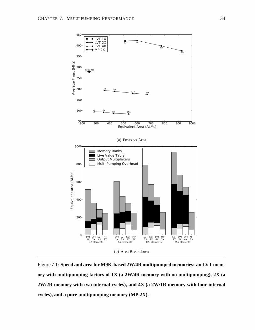
7.1 Speed and area for M9K-based 2W/4R multipumped memories. . . . . . . . . 34
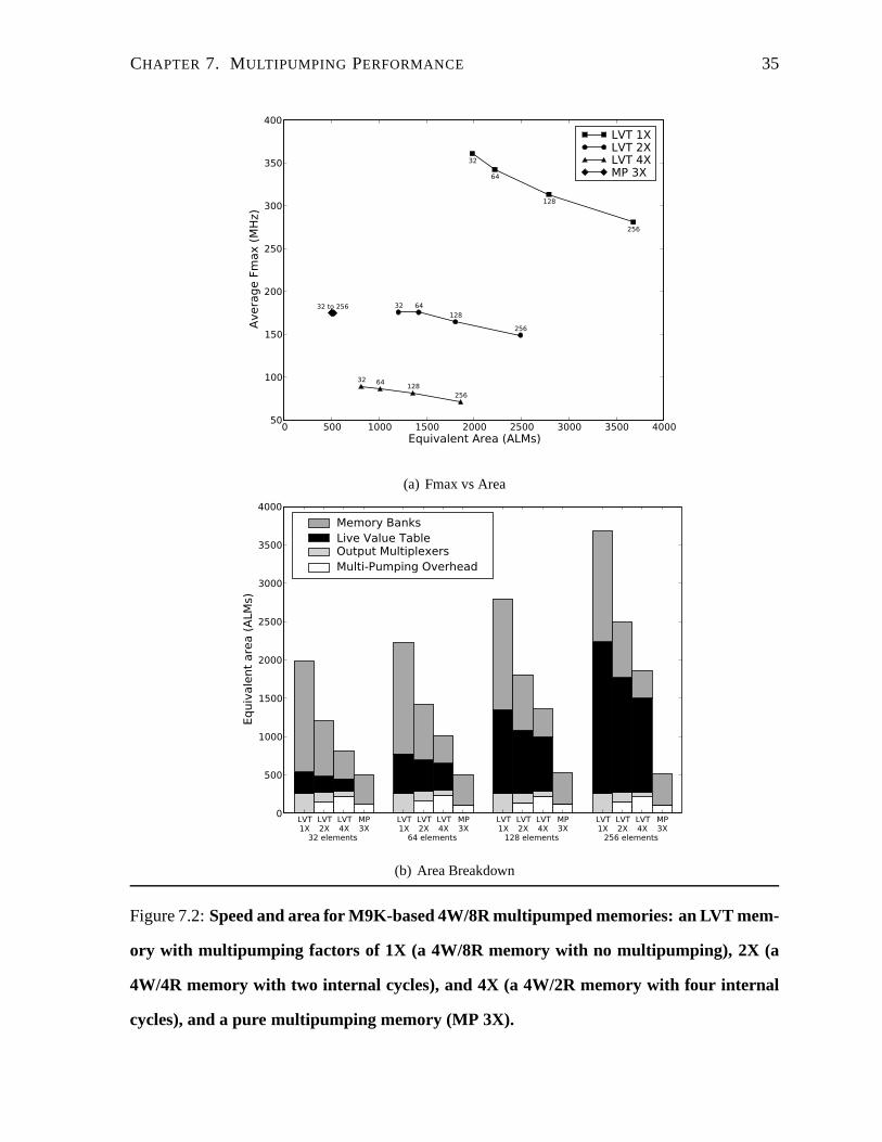
7.2 Speed and area for M9K-based 4W/8R multipumped memories. . . . . . . . . 35
vii
Chapter 1
Introduction
As FPGAs (Field-Programmable Gate Arrays) continue to increase in transistor density, de-
signers are using them to build larger and more complex systems-on-chip that require frequent
sharing, communication, queueing, and synchronization among distributed functional units
and compute nodes—for example, applications that include multiple FIFO buffers for moving
data between clock domains. These mechanisms are often bestimplemented withmulti-ported
memories—memories that allow multiple reads and writes to occur simultaneously—since they
can avoid serialization and contention.
As another example, processors normally require a multi-ported register file, where more
register file ports allows the processor to exploit a greateramount ofinstruction-level par-
allelism (ILP) where multiple instructions are being executed at thesame time. However,
FPGA-basedsoft processorshave so far exploited little ILP, limited mainly to simple instruc-
tion pipelines. This is partly due to the fact that multi-ported memories (register files, in this
case) are particularly inefficient to implement on FPGAs.
1.1 Conventional Approaches
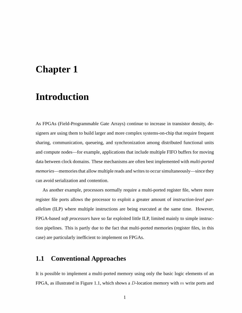
It is possible to implement a multi-ported memory using onlythe basic logic elements of an
FPGA, as illustrated in Figure 1.1, which shows aD-location memory withm write ports and
1
CHAPTER 1. INTRODUCTION 2
...
...
...
.
.
.
...
S0
S1
S2
...
...
Wm−1
W0
.
.
.
SD
R0
Rn−1
.
.
.
mW/nR
r
r
Figure 1.1: A multi-ported memory implemented with FPGA logic blocks, having D
single-word storage locations (S), m write (W ) ports, and n read (R) ports (encoded as
mW/nR), and n temporary registers r. Only read and write data lines are shown (i.e.,
not address lines).
n read ports. As shown, we requireD m-to-one decoders to steer writes to the appropriate
memory locations, andn D-to-one multiplexers to allow each read to access any memory
location. Note also that the read outputs are registered (r) to implement a synchronous memory
where the output is held stable between clock edges. The problem is that this circuit scales
very poorly, with area increasing rapidly with memory depth, and the decoding/multiplexing
severely limiting the maximum operating frequency.
It is normally more efficient to implement memories on FPGAs using the provided block
RAMs, each of which can be quite large (e.g., 9Kbits) while supporting high operating fre-
quencies (e.g., 580MHz). However, FPGA block RAMs currently provide only two ports
for reading and/or writing. Note that Altera’s Mercury lineof Programmable Logic Devices
(PLDs) [2] previously provided quad-port RAMs to support gigabit telecom applications—
however, this feature has not been supported in any other Altera device, likely due to the high
hardware cost.
CHAPTER 1. INTRODUCTION 3
M0 R0
...W0
n−1M Rn−1
1W/1R
1W/nR
1W/1R
(a) Replication
...
R0W0 M0
M m−1 Rn−1Wm−1
1W/1R
mW/nR
1W/1R
(b) Banking
M0r...r
...Wm−1
W1
W0 r...r
Rn−1
R0...Rn−2
1W/1R
mW/nR
(c) Multipumping
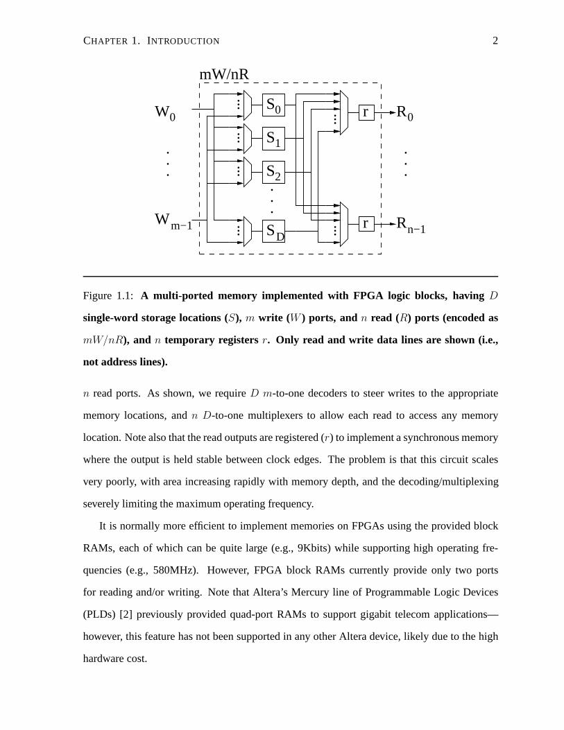
Figure 1.2:Three conventional techniques for providing more ports given a 1W/1R mem-
ory (read and write address values are not depicted, only data values): Replication (a)
maintains an extra copy of the memory to support each additional read port, but is lim-
ited to supporting only one write port; Banking (b) divides data across multiple memo-
ries, but each read or write port can only access one specific memory; Multipumping (c)
multiplies the number of read/write ports of a memory by adding internal data and ad-
dress multiplexers and temporary registers (r), and internally clocking the memory at a
multiple of the external clock (which quickly degrades the maximum external operating
frequency).
CHAPTER 1. INTRODUCTION 4
System designers have hence used one or a combination of three conventional techniques
for increasing the effective number of ports of FPGA block RAMs, as shown in Figure 1.2.
The first isreplication, which can increase the number of read ports by maintaining areplica
of the memory for each additional read port. However, this technique alone cannot support
more than one write port, since the one external write port must be routed to each block RAM
to keep it up-to-date. The second isbanking, which divides memory locations among multiple
block RAMs (banks), allowing each additional bank to support an additional read and write
port. However, with this approach each read or write port canonly access its corresponding
memory division—hence a pure banked design does not truly support sharing across ports.
The third we call“multipumping” , where any memory design is clocked at a multiple of the
external clock, providing the illusion of a multiple of the number of ports. For example, a
1W/1R memory can be internally clocked at 2X the external frequency to give the illusion of
being a 2W/2R memory. A multipumped design must also includemultiplexers and registers
to temporarily hold the addresses and data of pending reads and writes, and must carefully
define the semantics of the ordering of reads and writes. While reasonably straight-forward,
the drawback of a multipumped design is that each increase inthe number of ports dramatically
reduces the maximum external operating frequency of the memory.
1.2 A More Efficient Approach
In this dissertation we propose a new design for true multi-ported memories that capitalizes
on FPGA block RAMs while providing (i) substantially betterarea scaling than a pure logic-
based approach, and (ii) higher frequencies than the multipumping approach. The key to our
approach is a form of indirection through a structure calledtheLive Value Table(LVT), which
is itself a small multi-ported memory implemented in reconfigurable logic similar to Figure 1.1.
Essentially,the LVT allows a banked design to behave like a true multi-ported design by
directing reads to appropriate banks based on which bank holds the most recent or “live”
write value.
CHAPTER 1. INTRODUCTION 5
The intuition for why an LVT-based design is more efficient even though the LVT is imple-
mented in reconfigurable logic is because the LVT is much narrower than the actual memory
banks since it only holds bank numbers rather than full data values—thus the lines that are de-
coded/multiplexed are also much narrower and hence more efficiently placed and routed. An
LVT-based design also leverages block RAMs, which implement memory more efficiently, and
has an operating frequency closer to that of the block RAMs themselves. Additionally, an LVT-
based design and multipumping are complementary, and we will show that with multipumping
we can reduce the area of an LVT-based design by halving its maximum operating frequency.
With these techniques we can support soft solutions for multi-ported memories without the
need for expensive hardware block RAMs with more than two ports.
1.3 Research Goals
This research focuses on the implementation of efficient multi-ported memories for FPGAs.
We accomplish this through the following goals:
1. To explore the design space of multi-ported memories on FPGAs and evaluate the found
designs points in terms of speed and area.
2. To expand this design space by finding and evaluating new designs that are faster and
smaller than conventional approaches.
CHAPTER 1. INTRODUCTION 6
1.4 Organization
This dissertation is organized as follows: Chapter 2 reviews the existing work on FPGA and
CMOS implementations of multi-ported memories. Chapter 3 overviews the system we cre-
ated to generate ranges of designs. Chapter 4 describes the fundamental building blocks we
use in our implementations. Chapter 5 describes the theory and operation of Live Value Tables
and the multi-ported memories they enable. Chapter 6 compares the performance of different
implementations of Live Value Table-based memories. Chapter 7 compares the performance
of multipumping as implemented natively and as applied to Live Value Table-based memo-
ries. Chapter 8 summarizes our findings and design selections, and suggests potential future
directions for improvement.
Chapter 2
Background
Designers use Field Programmable Gate Arrays (FPGAs) to implement custom logic in cases
where it would cost too much or take too long to do so in Application-Specific Integrated Cir-
cuits (ASICs). Such cases include device prototyping, low-to-medium volume production, and
field-upgradable systems. As the size of the commercially available FPGAs have increased,
so have the size and complexity of the designs implemented. Conversely, as applications be-
came more demanding, FPGAs began including special-purpose hardware, such as RAM and
multiplier blocks, as part of their architecture. As a consequence, at some point it became cost-
effective in terms of hardware and development to implemententire processors on FPGAs to
execute complex applications. Supporting Instruction-Level Parallelism (ILP) in soft proces-
sors, which requires simultaneously feeding multiple execution units, was one of the original
impulses for the work in this dissertation. In this chapter,we review past work on multi-ported
memories on FPGA, compare our work to similar efforts for custom CMOS multi-ported mem-
ories, and discuss the FPGA architectural features relevant to our work.
2.1 Related FPGA Work
There are several prior attempts to implement multi-portedmemories in the context of FPGAs,
mainly for the purpose of soft processor register files. The main motivation is Instruction-Level
7
CHAPTER 2. BACKGROUND 8
Parallelism (ILP), where simultaneously executing multiple instructions requires multiple con-
current accesses to the contents of a register file.
Most soft uniprocessors without ILP or multithreading simply use replication to provide
the 1W/2R register file required to support a typical three-operand Instruction Set Architec-
ture (ISA). For example, Yiannacouras explores many customizations to the datapath of soft
processors [26] and compares them to the Altera’s NiosII family of soft processors [6].
Even soft processors with some ILP may only require a simple replicated 1W/2R regis-
ter file: Carli [9] describes a soft processor that uses Tomasulo’s algorithm to avoid stalls
due to dependencies between instructions and also enables some parallel execution of instruc-
tions on multiple execution units. However, the inputs and outputs of the instructions are still
read/written one-at-a-time, and thus no extra memory or register file ports are required.
One case where multiple instruction operands need to be simultaneously read and written
is a form of ILP known as Very Long Instruction Word (VLIW). A VLIW processor receives
instructions in contiguous groups stored in a single long word, hence the name. Each execution
unit is connected to one slot in the instruction word, and since the compiler has already sched-
uled the instructions to avoid dependencies, the executionunits can all proceed in parallel.
One such VLIW soft processor is from Joneset al. [13], where some of the execution units are
custom hardware designed to accelerate a specific application. Since the custom hardware is
accessible as just another instruction that can execute in parallel, the interfacing overhead with
the rest of the processor is effectively zero. This is one example of multi-ported memories en-
abling efficient communication between multiple functional units. However, their multi-ported
register file is implemented entirely using the FPGA’s reconfigurable logic and thus limits the
operating frequency of their soft processor.
On the other hand, Saghiret al. [21, 22] implement a fast multi-ported register file for a
VLIW soft processor by exploiting both replication and banking of block RAMs. However,
the banked architecture requires that the compiler schedule register accesses such that there
are no two simultaneous writes to the same bank, nor reads forthe same data originating from
CHAPTER 2. BACKGROUND 9
execution units connected to different banks. Nonetheless, this approach is sufficient to support
multithreading [11, 14, 17, 18], which is a rapid context switch between execution threads to
hide instructions with long latencies, since each thread need only read/write its own division
of the register file and only one thread is active at any one time.
To avoid such access conflicts, Manjikian describes a true random-access multi-ported reg-
ister file that exploits an aggressive form of multipumping by performing reads and writes on
consecutive rising and falling clock edges within a processor cycle [16]. His approach avoids
Write-After-Read (WAR) violations by performing all writes before reads. Unfortunately this
design requires that the entire system use multiple-phase clocking.
2.2 Related CMOS Work
Although much prior work on multi-ported memories exists for custom CMOS implementa-
tions, most of it focuses on reducing the area of processor register files to control their power
consumption and delay. Contrary to the previously outlinedwork with FPGAs, research on
custom CMOS multi-ported memories tries to find ways toreducethe number of ports and
does so using techniques that take advantage of processor microarchitectural features, such as
dynamic instruction scheduling, which are not usually found in soft processors due to the area
cost.
Built-in memories in FPGAs run at the same intrinsic speed than the surrounding reconfig-
urable logic, but since they do not suffer from interconnectdelay, they generally do not become
the bottleneck as on-chip memories do in custom CMOS systems. Also, the area density of
block RAMs is much higher than that of the surrounding systems built-up from the FPGA’s re-
configurable logic. Thus, even seemingly profligate duplication and partial use of block RAM
resources still have a moderate impact on the total area of a system. This difference from
custom CMOS frees us from having to primarily focus on savingarea.
CHAPTER 2. BACKGROUND 10
The techniques used for custom CMOS multi-ported memories include stream-oriented
hierarchical register file organization [20], storing small values directly in the register renaming
map entries [15], applying register renaming to entire banks of registers [8,19,25] or arbitrating
between several smaller multi-ported register files [24]1, using multiple banks to reduce the
number of ports per bank along with a second-level “victim cache” register file [7, 10], or
taking advantage of the fact that most register values are short-lived to buffer a reduced number
of registers [12].
Virtually all of these approaches also make use of the pipeline forwarding paths to reuse
recently calculated values without having to read them out of the register file, reducing the
number of read ports required. They also take advantage of the relatively low frequency of
instruction result writes to reduce the number of write ports at the expense of infrequent stalls
costing only a few percent in performance. Overall, all these approaches depend on exploit-
ing the properties of the processor datapath in which the register files find themselves, which
reduces their generality. In contrast, our multi-ported memories behave in an ideal manner,
without restriction on port selection or access patterns.
2.3 Stratix III Architecture
Although initially regular arrays of Boolean look-up tables, flip-flops, and programmable rout-
ing interconnect, FPGAs have evolved under performance pressure towards the inclusion of
“hard blocks” that implement particular functions directly in CMOS logic. In this dissertation,
we focus on the Altera Stratix III family and how these hard blocks affect which multi-ported
memories are practical. The concepts generally translate to the devices of other FPGA ven-
dors. For example, other than the different capacities, theblock RAMs in Xilinx’s Virtex-6
FPGAs would function identically for our purposes. Figure 2.1 [3] points out the main features
of the architecture of the Altera Stratix III devices and we describe the features relevant to
multi-ported memories:
1These approaches resemble ours, but target dynamically scheduled processors. Our approach does not dependon instruction scheduling.

CHAPTER 2. BACKGROUND 11
Figure 2.1:Floorplan of Stratix III FPGA
2.3.1 Adaptive Logic Modules (ALMs)
The Stratix III ALMs each contain two registers, some adder logic, and Look-Up Tables
(LUTs). Memory built using ALMs has virtually no constraints on capacity, configuration,
and number of ports, but pays a large area and speed penalty (Figure 1.1). The CAD tools may
also require a prohibitive amount of time (over an hour) to place and route such a memory.
CHAPTER 2. BACKGROUND 12
2.3.2 M9K and M144K Block RAMs (BRAMs)
Block RAMs are implemented directly in CMOS logic and have two ports that can each func-
tion either as a read or a write port. These memories use less area and run at a higher frequency
than ones created from ALMs, but do so at the expense of havinga fixed storage capacity and
number of ports. The Stratix III FPGA devices mostly containM9K block RAMs, which hold
nine kilobits of information in various widths and depths. At a width of 32 bits, an M9K holds
256 elements. Stratix III FPGAs also contain larger M144K blocks, which each hold 144 kilo-
bits (as 4k×32 for example), but exist in much fewer numbers than M9Ks. Atthe fastest speed
grade (C2), block RAMs can operate at up to 580MHz [4].
2.3.3 Memory Logic Array Blocks (MLABs)
The Stratix III FPGA architecture clusters its ALMs into Logic Array Blocks (LABs), each
containing ten ALMs. Some of the LABs can function either as agroup of ALMs or as a
single small block of memory, or Memory LAB (MLAB). MLABs provide a halfway point
between ALM and BRAM implementations: they are small, numerous, and widely distributed
like ALMs, but implement memory in a denser, constrained manner like BRAMs. A single
MLAB holds up to 20 words of 16 bits. Unlike other forms of memory, which perform all
operations on the rising edge of the clock, MLABs read on the rising edge and write on the
falling edge. MLABs best implement small shift registers and FIFO buffers and not arbitrarily
deep memories.
2.3.4 Phase and Delay Locked Loops (PLLs and DLLs)
Although not directly used to implement memory, DLLs control clock skew while PLLs can
multiply the frequency of a clock signal. In later chapters,we will use multiplied clocks to
expand the number of ports to a memory via “multipumping”.
Chapter 3
Experimental Framework
3.1 Memory Designs
In this dissertation we consider only memories of 32-bit element width, as this is common in
many computing systems and processors. We consider a range of multi-ported memory designs
that have at least one write port and two read ports (1W/2R) such that all ports are usable simul-
taneously within a single cycle. We do not consider one-write-one-read (1W/1W) memories as
they are trivial to implement with a single FPGA block RAM. Wealso do not consider mem-
ories that may stall (eg., take multiple cycles to return read values should they conflict with
concurrent writes), although such designs would be compelling future work. Additionally, we
assume that multiple writes to the same address do not occur and that their result is undefined
(similar to block RAMs). Each design is wrapped in a test harness such that all paths origi-
nate and terminate at registers, allowing us to ensure proper timing analysis and to test each
design for correctness. The Verilog sources are generic anddo not contain any Altera-specific
modules or annotations.
13
CHAPTER 3. EXPERIMENTAL FRAMEWORK 14
3.2 CAD FLow
We use Altera’s Quartus 9.0 to target the Altera Stratix IIIEP3SL340F1760C2, a large and
fast device that allows us to compare with published resultsfor the Nios II soft processor [5].
We do not bias the synthesis process to favour area or speed optimizations, nor perform any
circuit transformations such as retiming. We configured theplace and route process to make
a standard effort at fitting the design with only two constraints: (i) to avoid I/O pin regis-
ters to prevent artificially long paths that would affect theclock frequency, and (ii) to set the
target clock frequency to 1Ghz—an impossibly-high value for current Stratix III devices—to
optimize circuit layout for speed1. We report maximum operating frequency by averaging the
result of place/routes across ten different random seeds.
3.3 Measuring Area
We report area as thetotal equivalent area, which estimates the actual silicon area of a design
point: we calculate the sum of all the Adaptive Logic Modules(ALMs) plus the area of the
Block RAMs counted as their equivalent area in ALMs. Altera graciously provided the confi-
dential area equivalence of BRAMs for Stratix II. We extrapolated the unavailable Stratix III
area numbers from the Stratix II data and other confidential data.
1This approach was recommended by an experienced user of Quartus as more practical than iterated guessing.
Chapter 4
Conventional Multi-Porting
In this chapter, we discuss the existing approaches used to increase the number of ports on
memories on FPGAs. We describe, evaluate, and compare conventional implementations using
a single clock, as well as multipumping implementations with both a system clock and an
internal multiplied clock, and outline their respective uses and limitations as a prelude to the
discussion of our new approach.
4.1 Conventional Implementations
A simple two-ported memory, with one read and one write port (1W/1R) defines the basic con-
ceptual and physical unit of storage from which we build multi-ported memories. We assume
that each port may access any one location per cycle, and if a read and write to the same location
occur in the same cycle, the read port obtains the current contents of the location and the write
port overwrites the contents at the end of the cycle (“Write-After-Read” (WAR) operation).
The simplest multi-ported memory that we consider is a 1W/2Rmemory. This memory
is interesting because it is not naturally supported by FPGAstructures but is commonly used,
for example for soft processor register files. Figure 4.1 plots the area and operating frequency
of 1W/2R memories of varying depth (where the depth is indicated by the number next to
each point), and of varying implementation. We use these results to discuss the following
conventional techniques for building multi-ported memories on FPGAs:
15
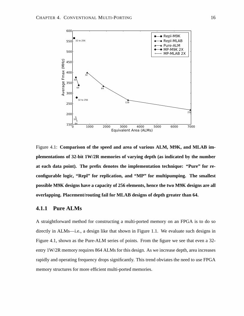
CHAPTER 4. CONVENTIONAL MULTI -PORTING 16
0 1000 2000 3000 4000 5000 6000 7000Equivalent Area (ALMs)
150
200
250
300
350
400
450
500
550
600
Aver
age
Fmax
(MHz
)
32 to 256
32
64
32
64
128
256
32 to 256
32
64
Repl-M9KRepl-MLABPure-ALMMP-M9K 2XMP-MLAB 2X
Figure 4.1: Comparison of the speed and area of various ALM, M9K, and MLAB im-
plementations of 32-bit 1W/2R memories of varying depth (asindicated by the number
at each data point). The prefix denotes the implementation technique: “Pure” for re-
configurable logic, “Repl” for replication, and “MP” for mul tipumping. The smallest
possible M9K designs have a capacity of 256 elements, hence the two M9K designs are all
overlapping. Placement/routing fail for MLAB designs of depth greater than 64.
4.1.1 Pure ALMs
A straightforward method for constructing a multi-ported memory on an FPGA is to do so
directly in ALMs—i.e., a design like that shown in Figure 1.1. We evaluate such designs in
Figure 4.1, shown as the Pure-ALM series of points. From the figure we see that even a 32-
entry 1W/2R memory requires 864 ALMs for this design. As we increase depth, area increases
rapidly and operating frequency drops significantly. This trend obviates the need to use FPGA
memory structures for more efficient multi-ported memories.
CHAPTER 4. CONVENTIONAL MULTI -PORTING 17
4.1.2 Replication
Replication (Figure 1.2(a)) is an easy way to increase the number of read ports of a simple
memory (i.e., to 1W/nR): simply provide as many copies of thememory as you require read
ports, and route the write port to all copies to keep them up-to-date. We evaluate replication
in Figure 4.1 for both M9Ks (Repl-M9K) and MLABs (Repl-MLAB). All of the Repl-M9K
designs fit into two M9K BRAMs, such that those points are all co-located in the figure. Repli-
cation requires no additional control logic, hence these designs are very efficient. For 1W/2R
memories with a depth greater than 256 elements, another pair of M9Ks would be added at
every depth increment of 256 elements—resulting in a relatively slow increase in area as mem-
ory depth increases. We also consider replicated designs composed of MLABs (Repl-MLAB).
Unfortunately, Quartus could not place and route any MLAB-based memory with more than 64
elements. Since each MLAB stores the equivalent of 160 ALMs,the Repl-MLAB implementa-
tion requires much less interconnect than the Pure-ALM implementation but considerably more
than the Repl-M9K implementation. For example, the 32-entry Repl-MLAB 1W/2R memory
requires only 198 equivalent ALMs, but still suffers a loweroperating speed of 376 MHz. The
replicated M9K designs (Repl-M9K) are evidently far superior to the alternatives, with an area
of 90 equivalent ALMs and maximum operating frequency of 564MHz. However, the draw-
back to this approach is that there is no way to provide additional write ports with replication
alone—we must pursue other techniques to provide more writeports.
4.1.3 Banking
Banking (Figure 1.2(b)) is similar to replication, except that the memory copies are not kept
coherent; this way, each additional memory supports an additional read and write port, provid-
ing an easy way to increase ports arbitrarily (mW/mR). The conventional way to use banking is
to divide memory locations evenly among the banks, such thateach read and write port are tied
to a certain memory division. However, a memory with only banking is not truly multi-ported,
CHAPTER 4. CONVENTIONAL MULTI -PORTING 18
since only one read from a certain division is possible in a given cycle. For this reason we do
not evaluate banked-only memories, although a close estimate of the Fmax/area of a mW/mR
banked memory is the corresponding 1W/mR replicated design.
4.1.4 Multipumping
Multipumping (Figure 1.2(c)) internally uses an integer multiple of the external system clock
to multiplex a multi-ported memory with fewer ports, givingthe external appearance of a larger
number of ports (mW/nR). This requires the addition of multiplexers and registers to hold tem-
porary states, as well as the generation of an internal clock, and careful management of the tim-
ing of read-write operations. We further describe the details of implementing a multipumped
design in the next section.
4.2 Multipumping Implementations
Since multipumped memories multiplex ports over time, the order that read/write operations
are performed must be carefully managed: violating the precedence of reads and writes would
break the external appearance of them occurring at the same time. In particular, writes must
be performed at the end to avoid Write-After-Read (WAR) violations where an earlier internal
write updates a value before it has been read by a subsequent internal read. Controlling the
sequence of internal reads and writes requires a Multipumping Controller (MPC), a small cir-
cuit that forcibly synchronizes two clock domains: one driven by a system clock and another
driven by a multiple of the system clock, with both clock domains in-phase and synchronous
to each other. One of the on-chip PLLs can easily generate such a relationship. The MPC
generates phase and write-enable signals alongside the multiplied clock to force the internal
operations controlled by the multiplied clock to occur witha certain phase relationship relative
to the external operations controlled by the system clock (e.g.: 1-2-3 1-2-3 . . . and not 2-3-1
2-3-1 . . . ).
CHAPTER 4. CONVENTIONAL MULTI -PORTING 19
For non-multipumped designs, each block RAM port supports either a read or a write,
hence we use the block RAMs in “simple dual-port” mode, wherea port is statically defined
to be for reading or writing. Since multipumped designs time-multiplex the block RAM ports
we can potentially exploit “true dual-port” mode, where a block RAM port can be dynamically
configured for reading or writing. In particular, we can use this feature to multipump a banked
design: use all of the ports of a banked design to perform reads until all of the reads are com-
plete, then use all the ports to perform writes such that all block RAMs are updated together. In
other words, the block RAMs are read like a banked memory and are written like a replicated
memory. Similar techniques have been published by Xilinx [23] and Actel [1] but only for cer-
tain forms of quad-port memories, whereas our implementation supports arbitrary numbers of
read and write ports. True dual-port mode is not free: for Stratix III FPGAs [4] an M9K block
RAM in simple dual-port mode has 256 locations of 32 bits, while in true dual-port mode it has
512 locations of 16 bits since the RAM output drivers are split to support two reads. Therefore
true dual-port mode requires two M9K block RAMs to create a 32-bit-wide memory. Despite
this doubling, the number of block RAMs required remains practical since it never needs to
exceed twice the number of read ports: one block RAM pair for every read port, as explained
below. Even an 8W/16R purely multipumped memory would need only 32 block RAMs.
The following summarizes the design of a pure multi-ported memory using true dual-port
mode for the block RAMs. Given an arbitrary mW/nR memory, thenumber of cycles required
to perform all them writes andn reads follows⌈m/2 + n/2x⌉, wherex counts the number
of block RAMs. Them/2 term stems from each write being replicated to all the block RAMs
to avoid data fragmentation, making the whole memory appearto have only two write ports.
Then/2x term comes from each block RAM being able to service any two reads at once since
the writes replicate their data to all block RAMs. The ceiling function handles cases where
there are either more internal ports than there are externalread or write ports, or the number
of internal ports does not evenly divide the number of external ports. A fractional number
of cycles in a term implies that, for one of the cycles, some ports remain free and some writes
CHAPTER 4. CONVENTIONAL MULTI -PORTING 20
might be done simultaneously with the last reads. The typical case is when the number of block
RAMs equals the number of read ports, allowing all reads to beperformed in one cycle while
leaving half the ports available for one of the writes, whichmay save one cycle in certain port
configurations. Larger numbers of block RAMs cannot furtherreduce the number of cycles,
which may become impractical for large numbers of ports due to the resulting low external
operating frequency.
As a simple example, in Figure 4.1 we implement 1W/2R memories by double-pumping
M9Ks (MP-M9K 2X) and MLABs (MP-MLAB 2X)1. While 2X multipumping does halve the
number of M9Ks or MLABs used, the additional overhead of the required control circuitry
negates any area savings for memories with so few ports. The maximum external operating
frequencies of the double-pumped designs are also a little under half those of the replicated
designs (186 MHz for MP-MLAB 2x, and 279 MHz for MP-M9K 2X). Aswe will demonstrate
later, multipumping can be an important technique to reducearea when building memories with
larger numbers of ports.
4.3 Summary
A 1W/2R memory can easily be extended to have more read ports by increasing the amount
of replication, but this technique cannot be used to add morewrite ports. A multi-ported
memory implemented purely in ALMs scales poorly. While banking easily allows multiple
write ports, such designs must map reads and writes to divisions of the memory, and do not
allow true sharing. Multipumping by itself causes a large drop in operating frequency. In the
next chapter, we introduce a method for transparently managing and keeping coherent banked
memories to effectively allow multiple readandwrite ports.
1Again, due to Quartus’ difficulty with MLABs, the multipumping implementation uses simpledual-portMLABs only. For 1W/2R only, this does not affect the area or external operation.
Chapter 5
LVT-Based Multi-Ported Memories
We propose a new approach to implementing multi-ported memories on FPGAs that can exploit
the strengths of all three conventional techniques for adding ports.Our approach comprises
banks of replicated block RAMs, where a mechanism of indirection steers reads to read
from the bank holding the most-recent value for a given location. Multipumping is orthog-
onal to our approach, and can be applied to reduce the area of amemory in cases where a
slower operating frequency can be tolerated, as we demonstrate later in Chapter 7. We name
our indirection mechanism theLive Value Table(LVT), since it tracks which bank contains the
“live” or most-recently updated value for each memory location.
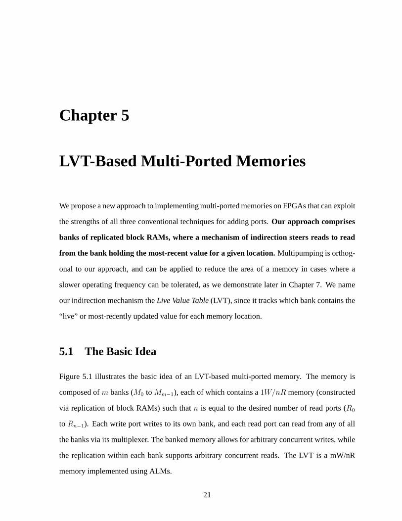
5.1 The Basic Idea
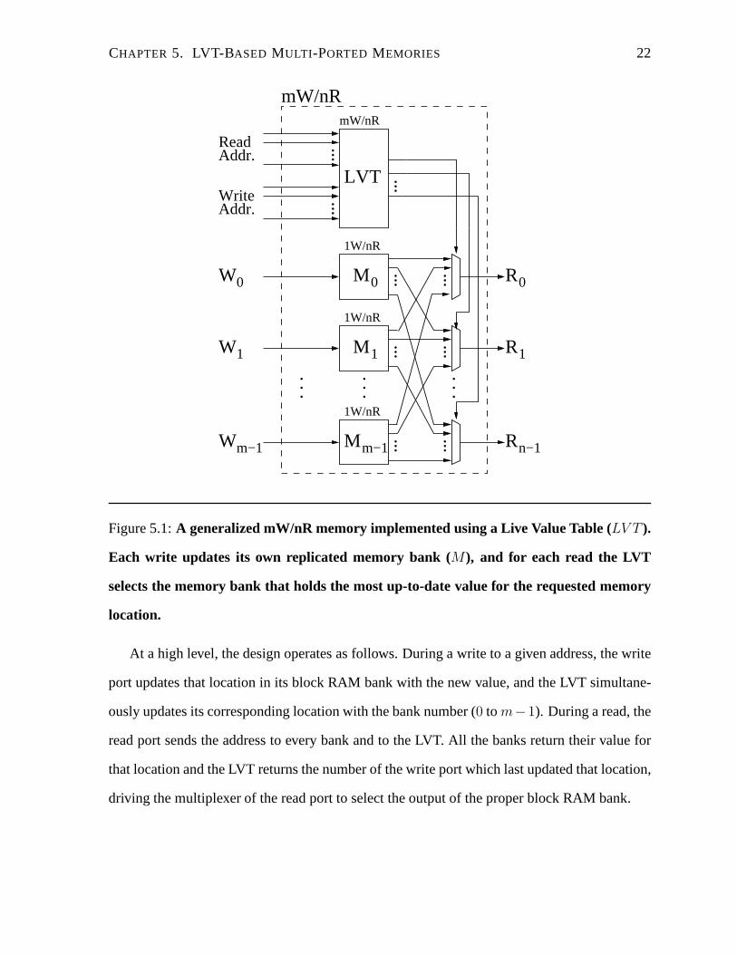
Figure 5.1 illustrates the basic idea of an LVT-based multi-ported memory. The memory is
composed ofm banks (M0 to Mm−1), each of which contains a1W/nR memory (constructed
via replication of block RAMs) such thatn is equal to the desired number of read ports (R0
to Rn−1). Each write port writes to its own bank, and each read port can read from any of all
the banks via its multiplexer. The banked memory allows for arbitrary concurrent writes, while
the replication within each bank supports arbitrary concurrent reads. The LVT is a mW/nR
memory implemented using ALMs.
21
CHAPTER 5. LVT-BASED MULTI -PORTED MEMORIES 22
..
.
M0
M1
Mm−1
..
.
... ...
... ...
Rn−1
R1
R0... ...
Wm−1
W1
W0
..
.
......
...
WriteAddr.
ReadAddr.
1W/nR
1W/nR
1W/nR
mW/nR
LVT
mW/nR
Figure 5.1:A generalized mW/nR memory implemented using a Live Value Table (LV T ).
Each write updates its own replicated memory bank (M), and for each read the LVT
selects the memory bank that holds the most up-to-date valuefor the requested memory
location.
At a high level, the design operates as follows. During a write to a given address, the write
port updates that location in its block RAM bank with the new value, and the LVT simultane-
ously updates its corresponding location with the bank number (0 to m−1). During a read, the
read port sends the address to every bank and to the LVT. All the banks return their value for
that location and the LVT returns the number of the write portwhich last updated that location,
driving the multiplexer of the read port to select the outputof the proper block RAM bank.
CHAPTER 5. LVT-BASED MULTI -PORTED MEMORIES 23
Addresses
Wm−1
W1
0W
......
b
D
d
d
d
mW/nR
Bank #
Bank #
Bank #
Bank #
(a) Write Operation
...
Addresses
R1
R0
R1
R0
Rn−1Rn−1
......
b
d
d
d
D b
b
b
mW/nR
Bank #
Bank #
Bank #
Bank #
Bank #
(b) Read Operation
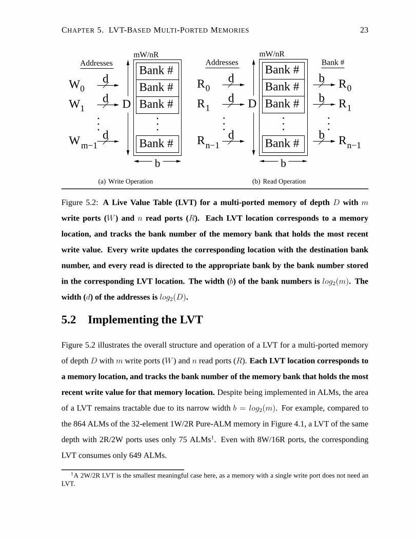
Figure 5.2: A Live Value Table (LVT) for a multi-ported memory of depth D with m
write ports (W ) and n read ports (R). Each LVT location corresponds to a memory
location, and tracks the bank number of the memory bank that holds the most recent
write value. Every write updates the corresponding location with the destination bank
number, and every read is directed to the appropriate bank bythe bank number stored
in the corresponding LVT location. The width (b) of the bank numbers islog2(m). The
width (d) of the addresses islog2(D).
5.2 Implementing the LVT
Figure 5.2 illustrates the overall structure and operationof a LVT for a multi-ported memory
of depthD with m write ports (W ) andn read ports (R). Each LVT location corresponds to
a memory location, and tracks the bank number of the memory bank that holds the most
recent write value for that memory location. Despite being implemented in ALMs, the area
of a LVT remains tractable due to its narrow widthb = log2(m). For example, compared to
the 864 ALMs of the 32-element 1W/2R Pure-ALM memory in Figure 4.1, a LVT of the same
depth with 2R/2W ports uses only 75 ALMs1. Even with 8W/16R ports, the corresponding
LVT consumes only 649 ALMs.
1A 2W/2R LVT is the smallest meaningful case here, as a memory with a single write port does not need anLVT.
CHAPTER 5. LVT-BASED MULTI -PORTED MEMORIES 24
During writes, the LVT uses the memory write addresses to update its corresponding
locations with the numbers of the ports performing the writes. These numbers identify the
block RAM banks that hold the most recently written values for those addresses. During
reads, the LVT uses the read addresses to fetch the bank numbers that in turn steer the
outputs of those banks to the read ports. All addresses are of width d = log2(D).
5.3 LVT Operation
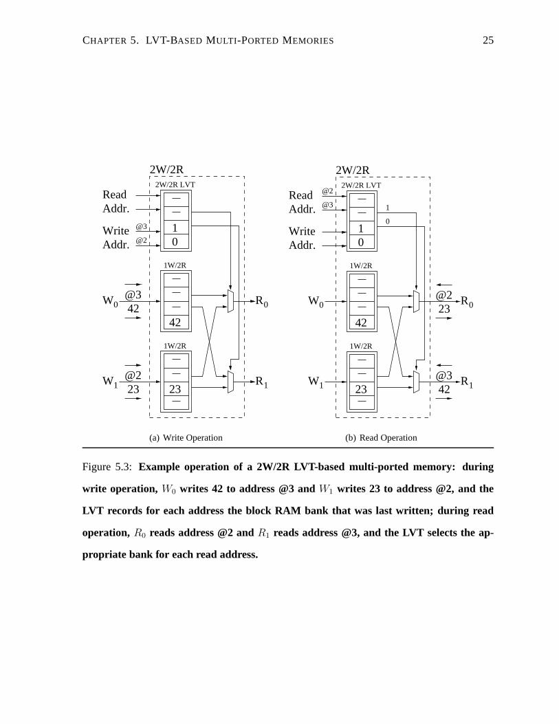
As an example of the operation of a Live Value Table, Figure 5.3 depicts two writes and two
reads to a multi-ported memory similar to the one depicted inFigure 5.1. The memory contains
one memory bank for each write port (W0 andW1). Each memory bank is a replicated block
RAM memory with enough ports for each read port (R0 and R1). The LVT at the top is
implemented using ALMs only, has the same depth as each memory bank, but stores the much
narrower bank numbers. The write ports place their bank number in the LVT at the same
address at which they write their data to the banks. The LVT controls the output multiplexer of
each read port. The memory begins empty or otherwise uninitialized.
Figure 5.3(a) shows the state of the memory banks and the LVT after portW0 writes the
value 42 to address 3 and portW1 writes 23 to address 2. The values are stored into the
separate memory banks of portsW0 andW1, while the LVT stores their bank numbers at the
same addresses.
An access from any read port will simultaneously send the address to the LVT and to each
memory bank. The bank number returned by the LVT directs the output multiplexer to select
the output of the block RAM memory bank containing the most current value for the second
memory element. In Figure 5.3(b), portR1 reads from address 3 and thus gets42 from bank0,
while portR0 reads from address 2 and gets23 from bank1.
CHAPTER 5. LVT-BASED MULTI -PORTED MEMORIES 25
W0
W1
R0
R1
2W/2R
42
0
@342
23
1W/2R
1W/2R
@2
@3
@2
1
23
ReadAddr.
WriteAddr.
2W/2R LVT
(a) Write Operation
R0
R1
W0
W1
1W/2R
2W/2R
42
0
@3
@2
@3
@2
42
23
1
0
1W/2R
1
23
WriteAddr.
ReadAddr.
2W/2R LVT
(b) Read Operation
Figure 5.3: Example operation of a 2W/2R LVT-based multi-ported memory: during
write operation, W0 writes 42 to address @3 andW1 writes 23 to address @2, and the
LVT records for each address the block RAM bank that was last written; during read
operation, R0 reads address @2 andR1 reads address @3, and the LVT selects the ap-
propriate bank for each read address.
CHAPTER 5. LVT-BASED MULTI -PORTED MEMORIES 26
5.4 Block RAM Requirements
Having memory banks which can hold the entire memory contents for each write port and
having each of these banks internally replicated once for each read port means that the total
number of block RAMs within all the banks equals the product of the number of write ports
and read ports, times the number of block RAMs necessary to hold the entire memory contents
in a single bank. This potentially cubic growth does not posean insurmountable problem
since the number of ports should remain modest in practice. For example, the rather large
case of a 32-bit 8W/16R multi-ported memory requires 128 block RAMs for depths of up
to 256 elements. Even the smallest Stratix III FPGA (EP3SL50) contains 108 M9K block
RAMs, while mid-range devices contain 275 to 355. The “Enhanced” (EP3SE) versions of
these FPGAs contain at least 400 M9K block RAMs. Also, the depth of the M9K block RAMs
greatly slows down their increase in numbers as the memory depth increases. For memories
holding several thousands of elements, deeper block RAMs such as the Stratix M144K might
be required. In Chapter 7, we will examine multipumping methods to reduce the number of
required block RAMs.
5.5 Recursive LVT Implementation
An LVT implements a multi-ported memory using ALMs and therefore grows proportionately
with depth—however, since each location stores only the fewbits required to encode a memory
bank number, the size of this memory remains practical. It would seem desirable to repeat
the area-saving process and implement the LVT itself using block RAMs, managed by a still
smaller, inner LVT. However, we cannot avoid implementing aLVT using ALMs since FPGAs
do not provide any suitable multi-ported block RAMs with enough write ports and the narrow
width to match the structure of a LVT. Ideally, a number of narrow mW/1r block RAMs could
be used together as a replicated memory to create a mW/nR memory and thus a LVT without
the use of ALM-based storage, but no such block RAMs exist on FPGAs. Additionally, any
CHAPTER 5. LVT-BASED MULTI -PORTED MEMORIES 27
inner LVT used to coordinate block RAMs implementing a larger outer LVT would necessarily
be implemented using ALMs and would have the same depth and control the same number of
banks and ports as the outer LVT it sought to replace. This inner LVT would thus have the
same area as the outer LVT, and hence is not worth it.
Chapter 6
LVT Performance
While an LVT does solve the problem of adding write ports to a memory, it also introduces
additional delay due to the bank number look-up and the read port multiplexers, and increases
the area due to internal replication of each memory bank. In this chapter and the next we
demonstrate that, despite this overhead, the LVT-based approach:
1. provides substantially better area scaling than a pure logic-based approach;
2. operates at higher frequencies than multipumping approaches.
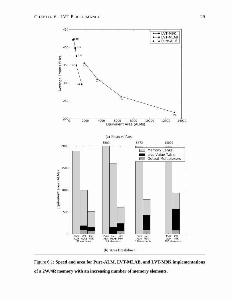
6.1 Speed vs. Area
Figure 6.1(a) and Figure 6.2(a) plot the average maximum operating frequency (Fmax) versus
area for 2W/4R and 4W/8R memories of increasing depth (denoted by the number next to the
data point). It is apparent that the pure ALM implementation(Pure-ALM) is inefficient: for the
4W/8R memory, 32 elements requires 3213 ALMs and 256 elements requires 23767 ALMs.
The larger of these pure ALM designs are likely too large to bepractical for most applications.
Looking at the MLAB-based LVT implementations (LVT-MLAB) for 2W/4R, the designs
are smaller but achieve a slower Fmax than the correspondingpure ALM designs due to inter-
connect delays between the multiple MLABs required to implement the full width and depth
28
CHAPTER 6. LVT PERFORMANCE 29
0 2000 4000 6000 8000 10000 12000 14000Equivalent Area (ALMs)
200
250
300
350
400
450
Aver
age
Fmax
(MHz
)
3264
128
256
32
64
32
64
128
256
LVT-M9KLVT-MLABPure-ALM
(a) Fmax vs Area
PureALM
LVTMLAB
32 elements
LVTM9K
PureALM
LVTMLAB
64 elements
LVTM9K
PureALM
128 elements
LVTM9K
PureALM
256 elements
LVTM9K
0
500
1000
1500
2000
Equi
vale
nt a
rea
(ALM
s)
1309264723501
Memory BanksLive Value TableOutput Multiplexers
(b) Area Breakdown
Figure 6.1:Speed and area for Pure-ALM, LVT-MLAB, and LVT-M9K implemen tations
of a 2W/4R memory with an increasing number of memory elements.
CHAPTER 6. LVT PERFORMANCE 30
0 5000 10000 15000 20000 25000Equivalent Area (ALMs)
150
200
250
300
350
400
Aver
age
Fmax
(MHz
)
32
64
128
25632
64
32
64
128
256
LVT-M9KLVT-MLABPure-ALM
(a) Fmax vs Area
PureALM
LVTMLAB
32 elements
LVTM9K
PureALM
LVTMLAB
64 elements
LVTM9K
PureALM
128 elements
LVTM9K
PureALM
256 elements
LVTM9K
0
1000
2000
3000
4000
5000
6000
7000
Equi
vale
nt a
rea
(ALM
s)
2376711456
Memory BanksLive Value TableOutput Multiplexers
(b) Area Breakdown
Figure 6.2:Speed and area for Pure-ALM, LVT-MLAB, and LVT-M9K implemen tations
of a 4W/8R memory with an increasing number of memory elements.
CHAPTER 6. LVT PERFORMANCE 31
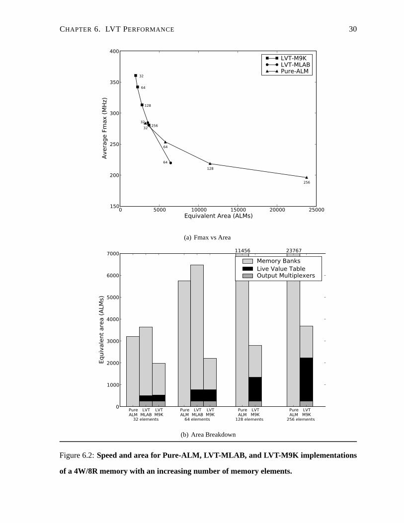
of a memory (see Section 2.3). For the 4W/8R designs, the MLAB-based LVT implementa-
tions are both larger and slower than the corresponding pureALM designs. Furthermore, the
MLAB-based designs cannot support memories deeper than 64 elements since Quartus can-
not place and route them. Overall the MLAB-based designs arenot compelling, except for
providing an area-Fmax trade-off relative to the pure ALM designs for 2W/4R memories.
From the figures it is evident that the M9K-based implementations are superior. The area
of the 2W/4R and 4W/8R LVT-M9K implementations increases much more slowly with depth
than the pure ALM implementation. The 2W/4R 32 and 64 elementimplementations are nearly
co-located probably because the only change is the width of the addresses from five to six bits,
and each ALM can calculate two Boolean functions of up to six inputs, matching the two
addresses from the write ports. Furthermore, as an indication of their usability, these designs
achieve a clock frequency close-to or better than the 290MHzclock frequency of a NiosII/f soft
processor on the same Stratix III device [5]. For example, the 4W/8R version has an operating
frequency ranging from 361 MHz at 32 elements, down to 281 MHzfor 256 elements, with
enough ports to supportfour such soft processors.
6.2 Area Breakdown
Figure 6.1(b) and Figure 6.2(b) display the total equivalent area of various implementations of
the same 2W/4R and 4W/8R memories, broken down into their components. The Pure-ALM
implementation is a single multi-ported memory without anyspecified sub-components: the
synthesis process implements all of the multiplexers, decoders, and storage implicitly. These
all increase in proportion with the depth of the memory and rapidly become impractically large.
The LVT-MLAB implementation, despite using denser memory,suffers from higher inter-
connect area overhead. The area of the LVT-MLAB memory banksincreases quickly along
with the memory depth since each MLAB can only store 20 words of 16 bits. Also, Quartus
could not place and route MLAB-based memories deeper than 64elements. The absence of
CHAPTER 6. LVT PERFORMANCE 32
output multiplexers for the 64-element 2W/4R memory is due to a fortuitous optimization by
Quartus: each register in an ALM has two load lines, which mayeliminate the multiplexer
when there are only two sources.
The LVT-M9K block RAM Memory Banks have the lowest area due totheir higher density
and lower interconnect requirements. Most of the multiplexing and decoding overhead in the
Pure-ALM and LVT-MLAB implementations becomes implicit inthe CMOS circuitry of the
M9K block RAMs. The area of the LVT-M9K 4W/8R Memory Banks remains constant at 1446
equivalent ALMs since all of the memory depths fit into the same number of block RAMs.
Even with the non-trivial overhead of the LVT, the LVT-M9K implementations consume much
less total area than the alternatives.
The LVTs of the LVT-MLAB and LVT-M9K implementations have the exact same internal
structure and the same depth as the corresponding Pure-ALM memory implementation and
thus also scale proportionately with the depth of the memory1. However, the LVTs only store
the one or two bits required to identify a memory bank, reducing their growth to tractable
levels. As an example, the area of the LVT of the LVT-M9K 4W/8Rmemory ranges from 280
ALMs up to 1977 ALMs: approximately one-tenth the area of thecorresponding Pure-ALM
memory. The area of the 4W/8R output multiplexers, when present, remains constant at 256
ALMs since the number of banks in the LVT-MLAB and LVT-M9K memories also remains
constant. For the 2W/4R memory, the multiplexer area fluctuates between 77 and 93 ALMs,
likely due to optimizations made possible when an ALM has only two inputs (one from each
bank).
1Slight area variations between the LVTs of comparable LVT-M9K and LVT-MLAB implementations arelikely due to place/route variations.
Chapter 7
Multipumping Performance
In the previous chapter we observed that M9K implementations of LVT-based multi-ported
memories are faster and smaller than the alternatives—in fact for some applications the achiev-
able Fmax is potentially overkill. In such cases we could potentially applymultipumping(as
introduced earlier in Section 4.1) to trade Fmax for reducedarea as the application allows. In
this chapter we describe and measure multipumping as applied to LVT-based designs, and also
compare with pure multipumping-based multi-ported memorydesigns.
7.1 Speed vs. Area
Multipumping can bring about a useful reduction in area if the speed of the original memory is
significantly higher than required by the surrounding system. Figure 7.1(a) and Figure 7.2(a)
compare the maximumexternaloperating frequency (Fmax) and the total area of M9K-based
LVT 2W/4R and 4W/8R memories with 2X and 4X multipumping, along with the equivalent
pure multipumping (MP) implementations. For all cases, theinternal operating frequency re-
mains approximately equal to the Fmax of the original baseline memory prior to multipumping,
which ranges for the LVT 4W/8R memory from 361 MHz to 281 MHz asthe depth increases,
and 523 MHz for all depths of the MP 3X 4W/8R memory. The MP implementations are
very nearly all co-located since all the memory depths fit into the same number of M9K block
RAMs. The small differences are due to the increasing width of addressing.
33
CHAPTER 7. MULTIPUMPING PERFORMANCE 34
200 300 400 500 600 700 800 900 1000Equivalent Area (ALMs)
50
100
150
200
250
300
350
400
450
Aver
age
Fmax
(MHz
)
32 64
128
256
32 64128 256
32 64 128 256
32 to 256
LVT 1XLVT 2XLVT 4XMP 2X
(a) Fmax vs Area
LVT1X
LVT2X
32 elements
LVT4X
MP2X
LVT1X
LVT2X
64 elements
LVT4X
MP2X
LVT1X
LVT2X
128 elements
LVT4X
MP2X
LVT1X
LVT2X
256 elements
LVT4X
MP2X
0
200
400
600
800
1000
Equi
vale
nt a
rea
(ALM
s)
Memory BanksLive Value TableOutput MultiplexersMulti-Pumping Overhead
(b) Area Breakdown
Figure 7.1:Speed and area for M9K-based 2W/4R multipumped memories: anLVT mem-
ory with multipumping factors of 1X (a 2W/4R memory with no mu ltipumping), 2X (a
2W/2R memory with two internal cycles), and 4X (a 2W/1R memory with four internal
cycles), and a pure multipumping memory (MP 2X).
CHAPTER 7. MULTIPUMPING PERFORMANCE 35
0 500 1000 1500 2000 2500 3000 3500 4000Equivalent Area (ALMs)
50
100
150
200
250
300
350
400
Aver
age
Fmax
(MHz
)
32
64
128
256
32 64128
256
32 64 128256
32 to 256
LVT 1XLVT 2XLVT 4XMP 3X
(a) Fmax vs Area
LVT1X
LVT2X
32 elements
LVT4X
MP3X
LVT1X
LVT2X
64 elements
LVT4X
MP3X
LVT1X
LVT2X
128 elements
LVT4X
MP3X
LVT1X
LVT2X
256 elements
LVT4X
MP3X
0
500
1000
1500
2000
2500
3000
3500
4000
Equi
vale
nt a
rea
(ALM
s)
Memory BanksLive Value TableOutput MultiplexersMulti-Pumping Overhead
(b) Area Breakdown
Figure 7.2:Speed and area for M9K-based 4W/8R multipumped memories: anLVT mem-
ory with multipumping factors of 1X (a 4W/8R memory with no mu ltipumping), 2X (a
4W/4R memory with two internal cycles), and 4X (a 4W/2R memory with four internal
cycles), and a pure multipumping memory (MP 3X).
CHAPTER 7. MULTIPUMPING PERFORMANCE 36
Despite the high internal operating frequencies, dividingthem by a multipumping factor
does bring about a harsh external speed penalty. For example, the 4W/8R LVT 2X multi-
pumped implementations in Figure 7.2(a) operate externally at frequencies ranging from 176
MHz to 149 MHz, which may still be practical speeds. The MP 3X implementations also hold
at 174 MHz. For either implementation, it is evident that only small multipumping factors can
be used before the drop in Fmax becomes too great to be practical. Although we have tested
multipumping factors of up to eight, we expect that most designs will use a factor of two or
three at most.
Furthermore, although the pure multipumping (MP) implementations seem to have better
performance and a greatly reduced area, a multipumping factor of two is only possible for
1W/2R (Figure 4.1) and 2W/4R memories (Figure 7.1(a)) because the underlying block RAMs
have only two ports. Pure multipumping memories with more ports will always require a mul-
tipumping factor of at least three or four, which will quickly drop the Fmax. By comparison,
a multipumping factor of two is always possible for any LVT memory with an even number
of read ports. The slower drop in speed of an LVT memory as the number of ports increases
(Figure 7.1(a) vs. Figure 7.2(a)) is a consequence of its greater internal parallelism, instead of
the mostly sequential operation of a pure multipumping memory.
7.2 Area Breakdown
The primary benefit of multipumping is reducing the area of the memory banks at the expense
of external clock frequency. Although the area of the memorybanks reduces proportionally to
the amount of multipumping, the LVT does not scale down as much and limits the overall area
reduction.
As discussed in Section 5.4, the number of block RAMs in a multi-ported LVT memory
is proportional to the product of the number of read and writeports. Since multipumping
divides the number of internal read ports, the number of block RAMs per bank is reduced by
CHAPTER 7. MULTIPUMPING PERFORMANCE 37
the same factor. This assumes the multipumping factor can evenly divide the number of read
ports. For example, a 4W/8R LVT memory supports factors of two, four, or eight only. The
number of read ports on the Live Value Table reduces to match,as does the number of output
multiplexers. Figure 7.1(b) and Figure 7.2(b) show how multipumping affects the area of each
of these components for the same LVT 2W/4R and 4W/8R memorieswhen using factors of
two (2X) and four (4X), compared to a factor of one (1X) as the baseline non-multipumped
case, which is identical to the LVT-M9K bars of Figure 6.1(b)and Figure 6.2(b). The figures
also show the area breakdown of the equivalent pure multipumping (MP) memories.
For LVT memories, the multipumping factor exactly divides the area of the memory banks
by itself since now only one-half or one-quarter the number of internal read ports exists, which
also reduces the area of the output multiplexers by the same ratio. For the 4W/8R memory,
the area of the Live Value Table shrinks by only 24% for 2X and 36% for 4X on average since
its number of write ports remains unchanged. This fact suggests that the narrower but more
numerous write port multiplexers and decoders have the largest impact on the area of memories
implemented using ALMs. The “Multipumping Overhead” fraction contains the additional
overhead of multipumping such as the Multipumping Controller, internal multiplexers, and
temporary registers. Regardless of the depth of the memory,multipumping introduces a small,
nearly constant overhead: 145 ALMs for 4W/8R LVT 2X multipumping, and 219 ALMs for
4W/8R LVT 4X on average. Summed together, these individual changes to the 4W/8R LVT
memories reduce the total area by an average of 36% for 2X multipumping, and 54% for 4X.
The unchanged number of write ports in the LVT primarily limits how much we can reduce the
area. In Section 8.2.2, we will propose a relaxation of read/write ordering to allow the number
of LVT and memory bank write ports to be reduced.
The pure multipumping memories (MP) use much less area sincethey do not require a
Live Value Table or Output Multiplexers, nor use as many block RAMs since their banks are
not replicated. For example, the 4W/8R MP 3X memory in Figure7.2(b) uses only eight
M9K block RAMs inside a total equivalent area of 511 ALMs, of which 105 are multipumping
CHAPTER 7. MULTIPUMPING PERFORMANCE 38
overhead. Unfortunately, pure multipumping memories tendto have higher minimum multi-
pumping factors and thus slower Fmax than LVT memories as thenumber of ports increases.
In Section 8.2.1, we will explore the idea of using pure multipumping memories with a small
number of ports to potentially improve the efficiency of LVT-based memories.
Chapter 8
Conclusions
FPGA systems provide efficient block RAMs, but with only two ports. Conventional ap-
proaches to building memories on FPGAs with a larger number of ports are either very area
inefficient, slow, or both. We introduced a smaller and faster implementation for multi-ported
memories based on the Live Value Table (LVT)—a small, narrow, multi-ported memory im-
plemented in logic elements that coordinates read and writeaccesses such that a block RAM
banked memory appears like a true multi-ported memory. The resulting multi-ported memories
provide true Write-After-Read (WAR) random access to any value, from an arbitrary number
of ports, without the need to schedule reads and writes.
For example, using a LVT controlling 32 M9K block RAMs, we were able to implement a
256-element 12-ported (4W/8R) multi-ported memory which operates at 281 MHz on Altera
Stratix III FPGAs while consuming an area equivalent to 3679ALMs: a 43% speed improve-
ment and 84% area reduction over the equivalent pure ALM implementation, and a 61% speed
improvement over a pure multipumping implementation, despite being 7.2x larger. The higher
speeds of our LVT-based designs presented the possibility of exchanging speed for area by ap-
plying multipumping. On average, 2X multipumping reduced the total area by 36%, while 4X
did so by 54%. Our designs also allowed for lower and more practical multipumping factors
than pure multipumping implementations as the number of ports increased.
39
CHAPTER 8. CONCLUSIONS 40
In summary, our exploration of the design space led us to three main conclusions:
1. LVT-based multi-ported memories are superior to logic-element-based designs in both
area and speed;
2. LVT-based implementations are faster than pure multipumping implementations although
with an area cost;
3. pure multipumping implementations can be sufficient if the number of required ports or
external operating frequency are modest.
8.1 Contributions
In this dissertation, we make the following contributions:
1. we present the first thorough exploration of the design space of FPGA multi-ported mem-
ories;
2. we evaluate conventional methods of building FPGA-basedmulti-ported memories and
confirm that they do not scale well;
3. we introduce theLive Value Table(LVT), an efficient mechanism for implementing
multi-ported memories with an arbitrary number of read and write ports without im-
posing any constraints on the order or location of reads and writes;
4. we demonstrate that LVT-based designs are smaller and faster than pure reconfigurable
logic implementations, as well as faster and more scalable than pure multipumping im-
plementations as the number of ports increases;
5. we evaluate the impact of multipumping on LVT-based designs to provide a complemen-
tary area/speed trade-off.
CHAPTER 8. CONCLUSIONS 41
8.2 Future Work
In this section we describe potential design avenues that are more aggressive than those we have
presented so far: a way to build an even more efficient LVT-based design using multipumping,
and relaxing read/write ordering to ease constraints on thedesign of the multi-ported memory.
8.2.1 LVT-Based Memory Based on Pure Multipumped Banks
If even moderately multi-ported block RAMs became available on FPGAs, some very signif-
icant area improvements to LVT-based multi-ported memories would follow. For example,
doubling the number of read and write ports on a block RAM would mean needing only half
as many memory banks to support the write ports of an LVT-based memory, with each bank
containing only half as many replicated memories to servicethe read ports, resulting in need-
ing only a quarter of the number of block RAMs necessary to construct a given LVT-based
multi-ported memory. Furthermore, halving the number of banks reduces the width of the LVT
by one bit. Given that a typical LVT has a width of only three bits or less, eliminating one will
significantly reduce its area.
Although most FPGAs do not provide block RAMs with more than two ports, some of
the smaller pure multipumping memories might provide usable substitutes. This speculation
is supported by the interesting performance of the ‘MP 2X’ 2W/4R pure multipumping de-
sign from Figure 7.1: 255 equivalent ALMs at 279 MHz, using four M9K block RAMs. If
we used this memory to construct the banks of the ‘LVT 1X’ 4W/8R LVT-based memory in
Figure 7.2, two banks would be required instead of four, witheach bank internally replicated
once to support the read ports, for a total of four 2W/4R memories. This sums to only 16 M9K
block RAMs instead of 32 for a conventional LVT-based implementation, and even including
the additional area overhead of multipumping1 the area of the memory banks would decrease
1This is the pessimistic case. For example, all of the multipumped memories could share a single multipump-ing controller.
CHAPTER 8. CONCLUSIONS 42
by 29%, while the area of the LVT would be halved. It is easy to see from Figure 7.2(b) that
these changes would significantly reduce the area of the 256-element 4W/8R ‘LVT 1X’ imple-
mentation. The impact on speed is harder to predict due to thelarge changes in the structure of
the memory banks, but it is conceivable that the operating frequency would remain near that of
the underlying 2W/4R pure multipumping memory.
8.2.2 Relaxed Read/Write Ordering
The primary obstacle to getting the most area benefit from multipumping is the relatively small
area reduction of the LVT since the number of write ports cannot be divided. The writes must
all occur together after the reads to prevent WAR violations. If we relax the read/write ordering
and allow writes to occur before all of the reads have completed, then time-multiplexing the
internal write ports becomes possible. The multipumping factor can now divide both the num-
ber of internal memory banks and the number of write ports on the Live Value Table, further
improving the area reduction of multipumping.
For example, with a multipumping factor of two and the read/write orderingpreserved,
our 4W/8R multi-ported memory example internally becomes a4W/4R memory. Halving the
number of read ports only halves thesizeof the memory banks and reduces the size of the
LVT to a lesser degree. By comparison, if we allow relaxed read/write ordering, then the
multipumping factor can also divide the number of write ports2, which will in turn divide the
numberof memory banks in addition to their size and further reduce the area of the LVT. In
effect, except for the small overhead of the multipumping control circuitry, the entire 4W/8R
memory would internally reduce to a 2W/4R instance which uses about 75% less hardware.
This quadratic area reduction is immediately visible when comparing the 2W/4R and 4W/8R
LVT entries in Figure 7.1(b) and Figure 7.2(b), as well as theLVT-M9K entries in Figure 6.1(b)
and Figure 6.2(b).
Relaxing the read/write ordering requires the designer to schedule the reads and writes
2This assumes that the multipumping factor can evenly dividethe number of write ports.
CHAPTER 8. CONCLUSIONS 43
to the multi-ported memory to avoid WAR violations which would corrupt data. For example,
given our 4W/8R example multi-ported memory with a multipumping factor of two and relaxed
read/write ordering, the reads and writes will internally execute as two consecutive 2W/4R
sets, each using one half of the external ports. If the designer wants to simultaneously read and
write to the same location within a system cycle, both operations must be grouped in the same
read/write set by performing them on the appropriate external ports. If the designer cannot do
this rearrangement, then the write operations must explicitly occur after the conflicting reads,
either by placing them in the following read/write set, or inthe next system cycle altogether.
Fortunately, this type of problem is identical to that of dependence analysis for optimizing
software loops, and should require no new techniques.
Bibliography
[1] Implementing Multi-Port Memories in ProASICPLUS Devices.http://www.actel.
com/documents/APA_MultiPort_AN.pdf, July 2003. Application Note AC176,
Accessed Sept. 2009.
[2] Mercury Programmable Logic Device Family Data Sheet.http://www.altera.
com/literature/ds/dsmercury.pdf, Jan 2003. Version 2.2, Accessed Sept.
2009.
[3] Stratix III FPGAs. http://www.altera.com/literature/br/
br-stratixIII.pdf, August 2007. Version 1.2, Altera brochure, Accessed
Sept. 2009.
[4] Stratix III Device Handbook Volume 1, Chapter 4: TriMatrix Embedded Memory
Blocks in Stratix III Devices. http://www.altera.com/literature/hb/
stx3/stx3_siii51004.pdf, May 2008. Version 1.8, Accessed Sept. 2009.
[5] Nios II Performance Benchmarks.http://www.altera.com/literature/ds/
ds_nios2_perf.pdf, June 2009. Version 4.0, Accessed Sept. 2009.
[6] Nios II Processor Reference Handbook. http://www.altera.com/
literature/hb/nios2/n2cpu_nii5v1.pdf, March 2009. Version 9.0,
Accessed Sept. 2009.
44
BIBLIOGRAPHY 45
[7] BALASUBRAMONIAN , R., DWARKADAS , S., AND ALBONESI, D. H. Reducing the
complexity of the register file in dynamic superscalar processors. InMICRO 34: Pro-
ceedings of the 34th annual ACM/IEEE international symposium on Microarchitecture
(Washington, DC, USA, 2001), IEEE Computer Society, pp. 237–248.
[8] BREACH, S. E., VIJAYKUMAR , T. N., AND SOHI, G. S. The anatomy of the register file
in a multiscalar processor. InMICRO 27: Proceedings of the 27th annual international
symposium on Microarchitecture(New York, NY, USA, 1994), ACM, pp. 181–190.
[9] CARLI , R. Flexible MIPS Soft Processor Architecture. Tech. rep.,Massachusetts Insti-
tute of Technology, Computer Science and Artificial Intelligence Laboratory, June 2008.
[10] CRUZ, J.-L., GONZALEZ , A., VALERO, M., AND TOPHAM, N. P. Multiple-banked
register file architectures. InISCA ’00: Proceedings of the 27th Annual International
Symposium on Computer Architecture(New York, NY, USA, 2000), ACM, pp. 316–325.
[11] FORT, B., CAPALIJA , D., VRANESIC, Z., AND BROWN, S. A Multithreaded Soft Pro-
cessor for SoPC Area Reduction. InFCCM ’06: 14th Annual IEEE Symposium on Field-
Programmable Custom Computing Machines(April 2006), pp. 131–142.
[12] FRANKLIN , M., AND SOHI, G. S. Register traffic analysis for streamlining inter-
operation communication in fine-grain parallel processors. In MICRO 25: Proceedings of
the 25th annual international symposium on Microarchitecture(Los Alamitos, CA, USA,
1992), IEEE Computer Society Press, pp. 236–245.
[13] JONES, A. K., HOARE, R., KUSIC, D., FAZEKAS, J.,AND FOSTER, J. An FPGA-based
VLIW processor with custom hardware execution. InFPGA ’05: Proceedings of the 2005
ACM/SIGDA 13th international symposium on Field-Programmable Gate Arrays(New
York, NY, USA, 2005), ACM, pp. 107–117.
BIBLIOGRAPHY 46
[14] LABRECQUE, M., AND STEFFAN, J. Improving Pipelined Soft Processors with Multi-
threading. InFPL 2007: International Conference on Field Programmable Logic and
Applications(Aug. 2007), pp. 210–215.
[15] L IPASTI, M. H., MESTAN, B. R., AND GUNADI , E. Physical Register Inlining. InISCA
’04: Proceedings of the 31st annual International Symposium on Computer Architecture
(Washington, DC, USA, 2004), IEEE Computer Society, p. 325.
[16] MANJIKIAN , N. Design Issues for Prototype Implementation of a Pipelined Superscalar
Processor in Programmable Logic. InPACRIM 2003: IEEE Pacific Rim Conference on
Communications, Computers and Signal Processing(Aug. 2003), vol. 1, pp. 155–158
vol.1.
[17] MOUSSALI, R., GHANEM , N., AND SAGHIR, M. Microarchitectural Enhancements for
Configurable Multi-Threaded Soft Processors. InFPL 2007: International Conference
on Field Programmable Logic and Applications(Aug. 2007), pp. 782–785.
[18] MOUSSALI, R., GHANEM , N., AND SAGHIR, M. A. R. Supporting multithreading in
configurable soft processor cores. InCASES ’07: Proceedings of the 2007 international
conference on Compilers, Architecture, and Synthesis for Embedded Systems(New York,
NY, USA, 2007), ACM, pp. 155–159.
[19] PALACHARLA , S., JOUPPI, N. P., AND SMITH , J. E. Complexity-effective superscalar
processors. InISCA ’97: Proceedings of the 24th annual International Symposium on
Computer Architecture(New York, NY, USA, 1997), ACM, pp. 206–218.
[20] RIXNER, S., DALLY , W., KHAILANY , B., MATTSON, P., KAPASI, U., AND OWENS, J.
Register organization for media processing. InHPCA-6: Proceedings of Sixth Interna-
tional Symposium on High-Performance Computer Architecture (2000), pp. 375–386.
BIBLIOGRAPHY 47
[21] SAGHIR, M., AND NAOUS, R. A Configurable Multi-ported Register File Architecture
for Soft Processor Cores. InARC 2007: Proceedings of the 2007 International Workshop
on Applied Reconfigurable Computing(March 2007), Springer-Verlag, pp. 14–25.
[22] SAGHIR, M. A. R., EL-MAJZOUB, M., AND AKL , P. Datapath and ISA Customiza-
tion for Soft VLIW Processors. InReConFig 2006: IEEE International Conference on
Reconfigurable Computing and FPGAs(Sept. 2006), pp. 1–10.
[23] SAWYER, N., AND DEFOSSEZ, M. Quad-Port Memories in Virtex Devices.
http://www.xilinx.com/support/documentation/application_
notes/xapp228.pdf, September 2002. XAPP228 (v1.0), Accessed Sept. 2009.
[24] TSENG, J. H.,AND ASANOVIC, K. Banked multiported register files for high-frequency
superscalar microprocessors. InISCA ’03: Proceedings of the 30th annual International
Symposium on Computer Architecture(New York, NY, USA, 2003), ACM, pp. 62–71.
[25] WALLACE , S., AND BAGHERZADEH, N. A Scalable Register File Architecture for Dy-
namically Scheduled Processors. InPACT ’96: Proceedings of the 1996 Conference on
Parallel Architectures and Compilation Techniques(Washington, DC, USA, 1996), IEEE
Computer Society, p. 179.
[26] Y IANNACOURAS, P., STEFFAN, J. G.,AND ROSE, J. Application-specific customiza-
tion of soft processor microarchitecture. InFPGA ’06: Proceedings of the 2006
ACM/SIGDA 14th international symposium on Field Programmable Gate Arrays(New
York, NY, USA, 2006), ACM, pp. 201–210.