Efficient Implementation of Analog Signal Processing Functions ... - Xilinx€¦ · sub-functions:...
13
WP442 (v1.0.2) March 16, 2018 www.xilinx.com 1 © Copyright 2013–2018 Xilinx, Inc. Xilinx, the Xilinx logo, Artix, ISE, Kintex, Spartan, Virtex, Vivado, Zynq, and other designated brands included herein are trademarks of Xilinx in the United States and other countries. MATLAB and Simulink are registered trademarks of The MathWorks, Inc. All other trademarks are the property of their respective owners. Despite increasing levels of system integration, many signal processing functions are still performed using discrete analog components on the PCB. With ever-increasing time-to-market and system cost reduction pressures, designing analog signal processing functions can sorely challenge a design team’s ability to meet both cost and performance requirements. In addition, these analog circuits are subject to tolerances, drift, and aging, all of which impact the accuracy of the system. Xilinx's Vivado® Design Suite and All Programmable Abstractions provide a powerful and easy to use methodology to address many of these analog design challenges while also reducing cost. And even designers with little FPGA or HDL experience can leverage tools like Vivado HLS and Vivado IP Integrator (IPI) to create flexible, accurate, robust analog/mixed-signal subsystems. White Paper: FPGAs and Zynq-7000 AP SoCs WP442 (v1.0.2) March 16, 2018 Efficient Implementation of Analog Signal Processing Functions in Xilinx All Programmable Devices By: Cathal Murphy
-
Upload
truonghanh -
Category
Documents
-
view
223 -
download
0
Transcript of Efficient Implementation of Analog Signal Processing Functions ... - Xilinx€¦ · sub-functions:...
WP442 (v1.0.2) March 16, 2018 www.xilinx.com 1
© Copyright 2013–2018 Xilinx, Inc. Xilinx, the Xilinx logo, Artix, ISE, Kintex, Spartan, Virtex, Vivado, Zynq, and other designated brands included herein are trademarks of Xilinx in the United States and other countries. MATLAB and Simulink are registered trademarks of The MathWorks, Inc. All other trademarks are the property of their respective owners.
Despite increasing levels of system integration, manysignal processing functions are still performed usingdiscrete analog components on the PCB. Withever-increasing time-to-market and system cost reductionpressures, designing analog signal processing functionscan sorely challenge a design team’s ability to meet bothcost and performance requirements. In addition, theseanalog circuits are subject to tolerances, drift, and aging,all of which impact the accuracy of the system.
Xilinx's Vivado® Design Suite and All ProgrammableAbstractions provide a powerful and easy to usemethodology to address many of these analog designchallenges while also reducing cost. And even designerswith little FPGA or HDL experience can leverage toolslike Vivado HLS and Vivado IP Integrator (IPI) to createflexible, accurate, robust analog/mixed-signalsubsystems.
White Paper: FPGAs and Zynq-7000 AP SoCs
WP442 (v1.0.2) March 16, 2018
Efficient Implementation of Analog Signal Processing Functions in
Xilinx All Programmable Devices
By: Cathal Murphy

2 www.xilinx.com WP442 (v1.0.2) March 16, 2018
Introduction
IntroductionMost systems need to be able to interact with the real world for the purpose of monitoring and controlling it. To allow this to happen, systems contain sensors that translate real-world stimuli, such as light, heat, and sound, into analog electrical signals. The analog outputs of these sensors need to be processed and digitized so that the appropriate information can be presented to the digital controller or processor. The analog processing and conditioning of the sensor output is done in many different ways, depending on factors such as the accuracy requirement and the type of sensor used. Common analog functions include:
• Level Translation (Bipolar to Single-Ended)
• Gain/Attenuation
• Bandwidth Limiting/Filtering/Noise Reduction
• Gain and Offset Error Cancellation
• Linearization
Analog Design ChallengesAnalog designers are typically tasked with designing and building the functions listed in the Introduction. To do so, they design circuits using various discrete components such as resistors, capacitors, and operational amplifiers mounted on the printed circuit board (PCB). This is a time-consuming process, involving many iterations and tweaks to ensure that the design delivers the correct specifications over component tolerances, temperature, and time. A lack of accurate analog simulation tools can further compound these issues.[Ref 1]
In addition, analog components introduce errors, such as noise, offset, and gain errors, into the measurement circuits. These error sources then impact the accuracy of the system or add additional calibration requirements.
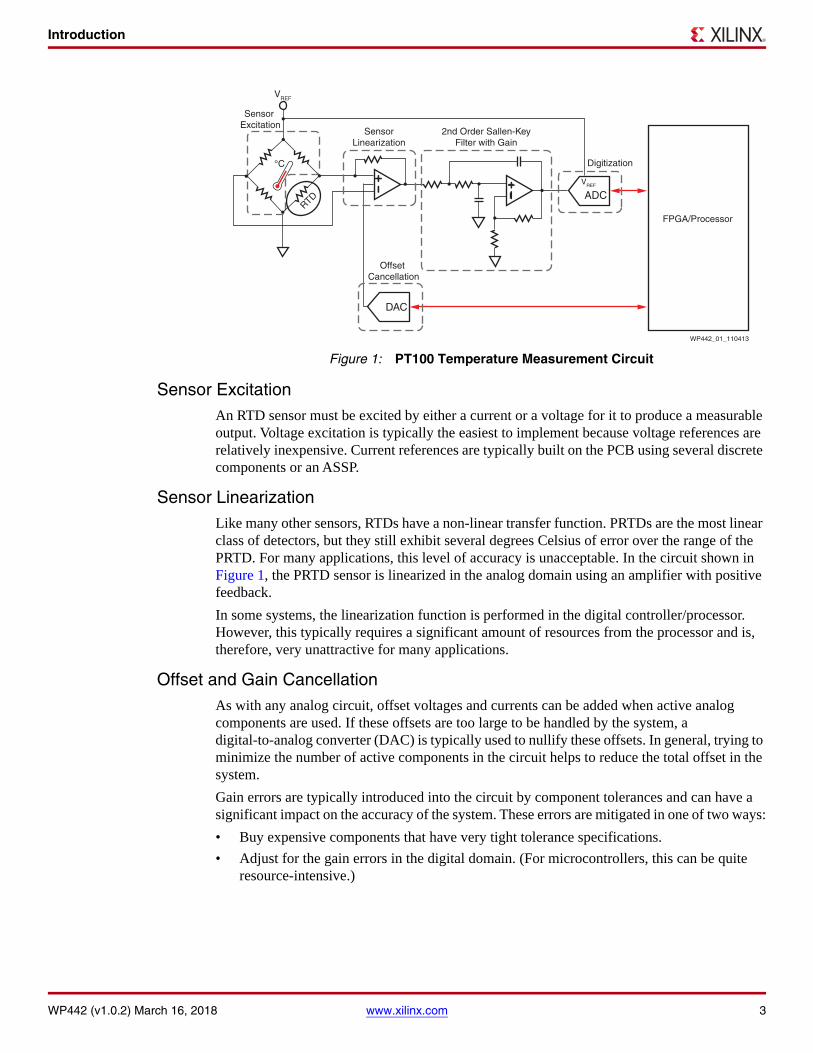
Temperature Sensor ExampleTo further illustrate what analog signal conditioning and processing typically looks like, a design to measure temperature using a resistance-to-temperature detector (RTD), shown in Figure 1, can be examined. An RTD is a sensor that changes its resistance as the temperature changes. Platinum resistance temperature detectors (PRTDs) are widely used because of their accuracy and their ability to operate over a very wide temperature range. The circuit shown in Figure 1 is typical of temperature- measuring designs that employ a PRTD. This circuit has five sub-functions: sensor excitation, linearization, offset cancellation, filtering, and digitization.
Introduction
WP442 (v1.0.2) March 16, 2018 www.xilinx.com 3
Sensor ExcitationAn RTD sensor must be excited by either a current or a voltage for it to produce a measurable output. Voltage excitation is typically the easiest to implement because voltage references are relatively inexpensive. Current references are typically built on the PCB using several discrete components or an ASSP.
Sensor LinearizationLike many other sensors, RTDs have a non-linear transfer function. PRTDs are the most linear class of detectors, but they still exhibit several degrees Celsius of error over the range of the PRTD. For many applications, this level of accuracy is unacceptable. In the circuit shown in Figure 1, the PRTD sensor is linearized in the analog domain using an amplifier with positive feedback.
In some systems, the linearization function is performed in the digital controller/processor. However, this typically requires a significant amount of resources from the processor and is, therefore, very unattractive for many applications.
Offset and Gain CancellationAs with any analog circuit, offset voltages and currents can be added when active analog components are used. If these offsets are too large to be handled by the system, a digital-to-analog converter (DAC) is typically used to nullify these offsets. In general, trying to minimize the number of active components in the circuit helps to reduce the total offset in the system.
Gain errors are typically introduced into the circuit by component tolerances and can have a significant impact on the accuracy of the system. These errors are mitigated in one of two ways:
• Buy expensive components that have very tight tolerance specifications.
• Adjust for the gain errors in the digital domain. (For microcontrollers, this can be quite resource-intensive.)
X-Ref Target - Figure 1
Figure 1: PT100 Temperature Measurement Circuit
VREF
DAC
ADC
WP442_01_110413
RTD
Sensor Excitation
°C
2nd Order Sallen-KeyFilter with Gain
Offset Cancellation
Digitization
FPGA/Processor
VREF
SensorLinearization
4 www.xilinx.com WP442 (v1.0.2) March 16, 2018
Introduction
Analog Filters Unlike digital systems, analog circuits are very susceptible to noise due to power supply variations and EMI. In addition, nearly all electrical components, such as resistors and amplifiers, add white noise to the signal. Therefore, analog signals can contain a lot of unwanted content, which impacts the accuracy of the system. To minimize the impact of this unwanted content or noise, filtering techniques are widely used.
Because temperature typically changes relatively slowly, all of the important information to be extracted from the measurements is at a low frequency. Thus, any high-frequency content can be considered noise content and filtered out using a low-pass filter.
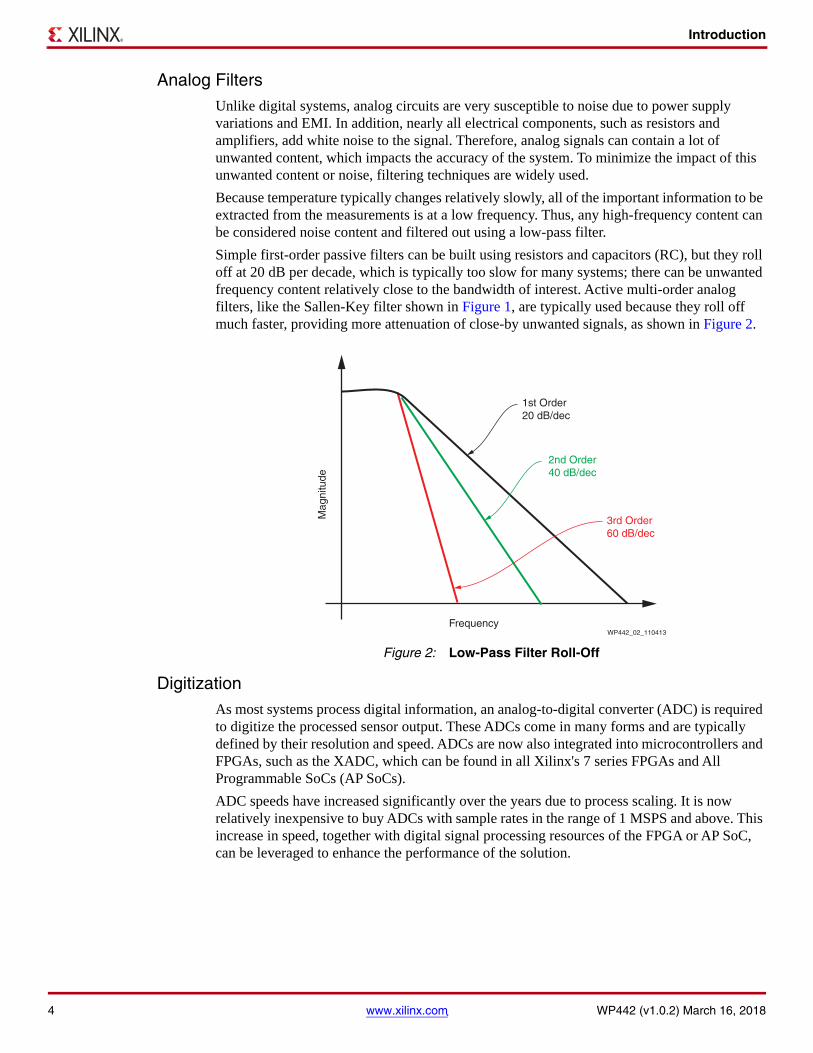
Simple first-order passive filters can be built using resistors and capacitors (RC), but they roll off at 20 dB per decade, which is typically too slow for many systems; there can be unwanted frequency content relatively close to the bandwidth of interest. Active multi-order analog filters, like the Sallen-Key filter shown in Figure 1, are typically used because they roll off much faster, providing more attenuation of close-by unwanted signals, as shown in Figure 2.
DigitizationAs most systems process digital information, an analog-to-digital converter (ADC) is required to digitize the processed sensor output. These ADCs come in many forms and are typically defined by their resolution and speed. ADCs are now also integrated into microcontrollers and FPGAs, such as the XADC, which can be found in all Xilinx's 7 series FPGAs and All Programmable SoCs (AP SoCs).
ADC speeds have increased significantly over the years due to process scaling. It is now relatively inexpensive to buy ADCs with sample rates in the range of 1 MSPS and above. This increase in speed, together with digital signal processing resources of the FPGA or AP SoC, can be leveraged to enhance the performance of the solution.
X-Ref Target - Figure 2
Figure 2: Low-Pass Filter Roll-Off
Mag
nitu
de
Frequency
1st Order20 dB/dec
2nd Order40 dB/dec
3rd Order60 dB/dec
WP442_02_110413
Analog Signal Processing Design in Xilinx FPGAs and AP SoCs
WP442 (v1.0.2) March 16, 2018 www.xilinx.com 5
Analog Signal Processing Design in Xilinx FPGAs and AP SoCsUntil recently, developing signal processing algorithms in an FPGA or SoC could be time consuming, especially for designers with little FPGA or HDL experience. Because of this, many designers have not explored the possibilities of using the signal process capabilities of FPGA or SoC devices to replace discrete analog functionality.
With All Programmable Abstractions, Xilinx empowers a host of new designers to design and build complex systems quickly and easily in Xilinx FPGAs and AP SoCs, even without much FPGA or HDL experience. With these abstractions, digital signal processing functions can be designed as pieces of IP that replace a discrete analog signal processing functionality. These pieces of IP can be realized in a number of ways:
• Taken directly from a catalog of commonly used functions (Vivado IP catalog) and customized via an easy-to-use GUI/Design Wizard
• C code-based IP generation with the Vivado High-Level Synthesis (HLS) tool
• Model-based design with MathWorks MATLAB® and Simulink®
Revisiting the RTD example circuit shown in Figure 1, it is useful now to see what analog functions can be moved from discrete implementations on a PCB to efficient digital signal processing in Xilinx FPGAs and/or AP SoCs, with the key functions of filtering and linearization examined first.
Enhanced Filtering CapabilitiesAs mentioned in Analog Filters, like many other sensors, the information of interest from a temperature sensor is all at lower frequencies. Thus, applying a low-pass filter to the signal improves the accuracy of the system by removing unwanted high-frequency noise.
It is widely known that implementing high-order, near-ideal filters in an FPGA is relatively easy and inexpensive. Consequently, the question might well occur: Why can't the analog filtering on the board be removed and replaced directly with a high-order digital FIR filter? The answer is, it can — but care must be taken to ensure the desired results are achieved. As this is a sampled system, the Nyquist-Shannon sampling theorem holds true, meaning care must be taken to minimize aliasing effects.[Ref 2]
AnalysisThe circuit shown in Figure 1 shows a second-order Sallen-Key low-pass analog filter. The filter is implemented using an operational amplifier and several resistors and capacitors. This filter is used to minimize unwanted noise and to prevent anti-aliasing effects when the signal is digitized. If the FPGA or AP SoC signal processing resources are utilized along with a higher-speed ADC (see the Digitization section), then a simpler, more accurate, more efficient solution can be realized.
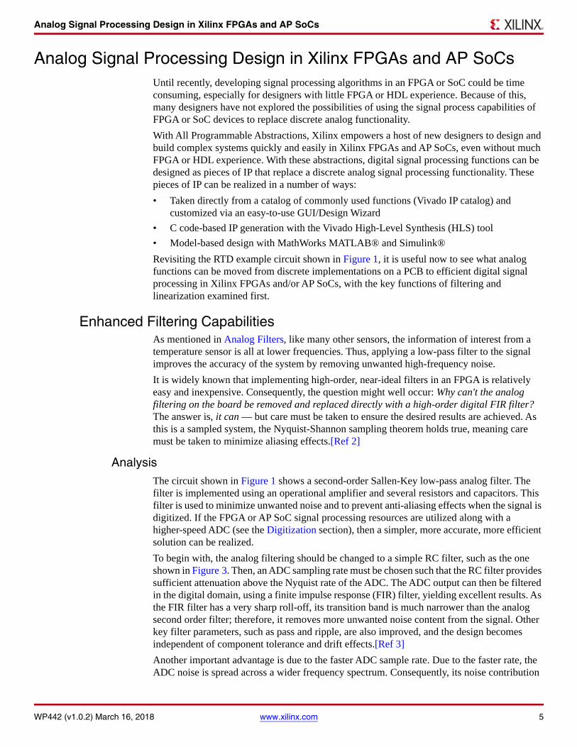
To begin with, the analog filtering should be changed to a simple RC filter, such as the one shown in Figure 3. Then, an ADC sampling rate must be chosen such that the RC filter provides sufficient attenuation above the Nyquist rate of the ADC. The ADC output can then be filtered in the digital domain, using a finite impulse response (FIR) filter, yielding excellent results. As the FIR filter has a very sharp roll-off, its transition band is much narrower than the analog second order filter; therefore, it removes more unwanted noise content from the signal. Other key filter parameters, such as pass and ripple, are also improved, and the design becomes independent of component tolerance and drift effects.[Ref 3]
Another important advantage is due to the faster ADC sample rate. Due to the faster rate, the ADC noise is spread across a wider frequency spectrum. Consequently, its noise contribution
6 www.xilinx.com WP442 (v1.0.2) March 16, 2018
Analog Signal Processing Design in Xilinx FPGAs and AP SoCs
over a fixed bandwidth is always better than that of a slower ADC with the same noise specification.
Thus, via filtering and decimation, the overall noise contribution of the ADC can be significantly reduced.[Ref 4] This can either lead to more accurate results, if that is necessary, or to a lower-cost design where the signal to noise ratio target has not changed.
Figure 3 shows the new improved design block diagram.
FIR Complier Design FlowXilinx FPGAs and AP SoCs can operate at many multiples of the 1–10MS/s, a sample rate typical of many contemporary ADCs. Because of this, the resources needed to design the filter can be time-multiplexed to build a very resource-efficient implementation.
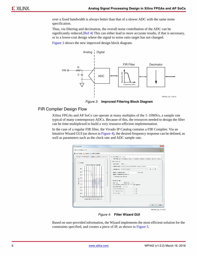
In the case of a regular FIR filter, the Vivado IP Catalog contains a FIR Complier. Via an Intuitive Wizard GUI (as shown in Figure 4), the desired frequency response can be defined, as well as parameters such as the clock rate and ADC sample rate.
Based on user-provided information, the Wizard implements the most efficient solution for the constraints specified, and creates a piece of IP, as shown in Figure 5.
X-Ref Target - Figure 3
Figure 3: Improved Filtering Block Diagram
Mag
nitu
de (
dB)
Frequency (kHz)
ADC
VINR
C
Analog Digital
FIR Filter Decimator
WP442_03_110413
X-Ref Target - Figure 4
Figure 4: Filter Wizard GUI
WP442_04_111313
Analog Signal Processing Design in Xilinx FPGAs and AP SoCs
WP442 (v1.0.2) March 16, 2018 www.xilinx.com 7
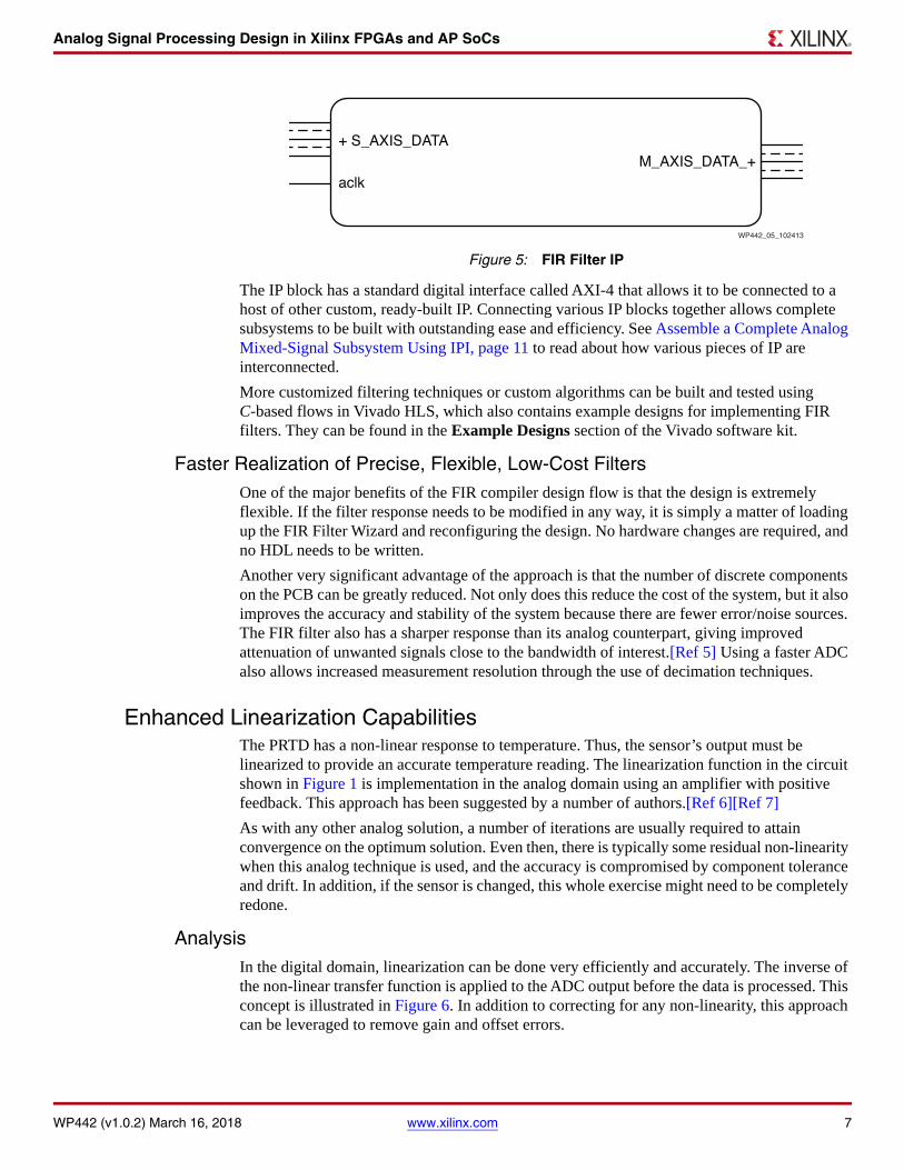
The IP block has a standard digital interface called AXI-4 that allows it to be connected to a host of other custom, ready-built IP. Connecting various IP blocks together allows complete subsystems to be built with outstanding ease and efficiency. See Assemble a Complete Analog Mixed-Signal Subsystem Using IPI, page 11 to read about how various pieces of IP are interconnected.
More customized filtering techniques or custom algorithms can be built and tested using C-based flows in Vivado HLS, which also contains example designs for implementing FIR filters. They can be found in the Example Designs section of the Vivado software kit.
Faster Realization of Precise, Flexible, Low-Cost Filters One of the major benefits of the FIR compiler design flow is that the design is extremely flexible. If the filter response needs to be modified in any way, it is simply a matter of loading up the FIR Filter Wizard and reconfiguring the design. No hardware changes are required, and no HDL needs to be written.
Another very significant advantage of the approach is that the number of discrete components on the PCB can be greatly reduced. Not only does this reduce the cost of the system, but it also improves the accuracy and stability of the system because there are fewer error/noise sources. The FIR filter also has a sharper response than its analog counterpart, giving improved attenuation of unwanted signals close to the bandwidth of interest.[Ref 5] Using a faster ADC also allows increased measurement resolution through the use of decimation techniques.
Enhanced Linearization CapabilitiesThe PRTD has a non-linear response to temperature. Thus, the sensor’s output must be linearized to provide an accurate temperature reading. The linearization function in the circuit shown in Figure 1 is implementation in the analog domain using an amplifier with positive feedback. This approach has been suggested by a number of authors.[Ref 6][Ref 7]
As with any other analog solution, a number of iterations are usually required to attain convergence on the optimum solution. Even then, there is typically some residual non-linearity when this analog technique is used, and the accuracy is compromised by component tolerance and drift. In addition, if the sensor is changed, this whole exercise might need to be completely redone.
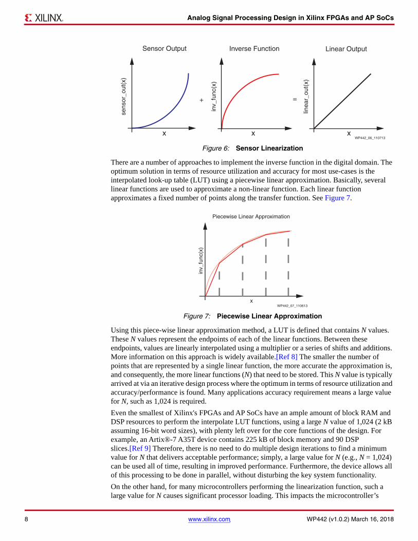
AnalysisIn the digital domain, linearization can be done very efficiently and accurately. The inverse of the non-linear transfer function is applied to the ADC output before the data is processed. This concept is illustrated in Figure 6. In addition to correcting for any non-linearity, this approach can be leveraged to remove gain and offset errors.
X-Ref Target - Figure 5
Figure 5: FIR Filter IP
+ S_AXIS_DATAM_AXIS_DATA_+
aclk
WP442_05_102413
8 www.xilinx.com WP442 (v1.0.2) March 16, 2018
Analog Signal Processing Design in Xilinx FPGAs and AP SoCs
There are a number of approaches to implement the inverse function in the digital domain. The optimum solution in terms of resource utilization and accuracy for most use-cases is the interpolated look-up table (LUT) using a piecewise linear approximation. Basically, several linear functions are used to approximate a non-linear function. Each linear function approximates a fixed number of points along the transfer function. See Figure 7.
Using this piece-wise linear approximation method, a LUT is defined that contains N values. These N values represent the endpoints of each of the linear functions. Between these endpoints, values are linearly interpolated using a multiplier or a series of shifts and additions. More information on this approach is widely available.[Ref 8] The smaller the number of points that are represented by a single linear function, the more accurate the approximation is, and consequently, the more linear functions (N) that need to be stored. This N value is typically arrived at via an iterative design process where the optimum in terms of resource utilization and accuracy/performance is found. Many applications accuracy requirement means a large value for N, such as 1,024 is required.
Even the smallest of Xilinx's FPGAs and AP SoCs have an ample amount of block RAM and DSP resources to perform the interpolate LUT functions, using a large N value of 1,024 (2 kB assuming 16-bit word sizes), with plenty left over for the core functions of the design. For example, an Artix®-7 A35T device contains 225 kB of block memory and 90 DSP slices.[Ref 9] Therefore, there is no need to do multiple design iterations to find a minimum value for N that delivers acceptable performance; simply, a large value for N (e.g., N = 1,024) can be used all of time, resulting in improved performance. Furthermore, the device allows all of this processing to be done in parallel, without disturbing the key system functionality.
On the other hand, for many microcontrollers performing the linearization function, such a large value for N causes significant processor loading. This impacts the microcontroller’s
X-Ref Target - Figure 6
Figure 6: Sensor Linearization
X-Ref Target - Figure 7
Figure 7: Piecewise Linear Approximation
sens
or_o
ut(x
)
x
Sensor Output Inverse Function Linear Output
+ =
inv_
func
(x)
x
linea
r_ou
t(x)
WP442_06_110713x
Piecewise Linear Approximation
WP442_07_110613
inv_
func
(x)
x
Analog Signal Processing Design in Xilinx FPGAs and AP SoCs
WP442 (v1.0.2) March 16, 2018 www.xilinx.com 9
ability to perform its core functions, driving users to a more expensive solution. Microcontrollers can have as little as 8 kB of memory and only a single multiplier that requires a number of processor cycles to execute. Since the microcontrollers are likely to have a host of other tasks to execute, it is unlikely to be able to service the ADC data very regularly; thus, data throughput is likely to be very limited. This might be acceptable for a temperature sensor, yet be completely unacceptable for other forms of sensors.
Vivado HLS Design FlowThere are a number of implementation options for the linearization function, including Vivado HLS and System Generator. For this particular example, Vivado HLS is used. Vivado HLS accelerates IP creation by enabling C, C++, and System C specifications to be targeted directly into Xilinx FPGAs and AP SoCs, eliminating the need to create RTL manually.
To build an interpolated LUT function, there are two steps:
1. Calculating the appropriate LUT values
2. Designing the interpolated LUT function
Microsoft Excel, MathWorks MATLAB, or C can be leveraged to generate the appropriate LUT data for a given non-linearity. Again, a LUT size of 1,024 is recommended because this size delivers the accuracy required by nearly all applications, and it uses only a fraction of the FPGA or SoC resources.
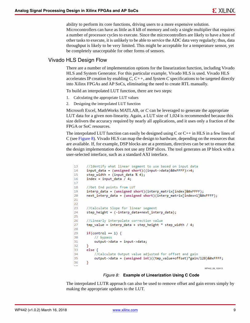
The interpolated LUT function can easily be designed using C or C++ in HLS in a few lines of C (see Figure 8). Vivado HLS can map the design to hardware, depending on the resources that are available. If, for example, DSP blocks are at a premium, directives can be set to ensure that the design implementation does not use any DSP slices. The tool generates an IP block with a user-selected interface, such as a standard AXI interface.
The interpolated LUTR approach can also be used to remove offset and gain errors simply by making the appropriate updates to the LUT.
X-Ref Target - Figure 8
Figure 8: Example of Linearization Using C Code
WP442_08_102413
10 www.xilinx.com WP442 (v1.0.2) March 16, 2018
Putting the Entire Analog Mixed-Signal Subsystem Together
In addition, an example solution using System Generator can be found in XCELL Journal 68.[Ref 10]
Faster Realization of Precise, Flexible, Low-Cost Linearization Functions The interpolated LUT approach using HLS enables the linearization function to be designed extremely quickly and efficiently. In addition, if the sensor changes, the LUT can easily be recalculated and then updated via the data-to-memory function in the Vivado IP integrator, making for an extremely flexible design. See Assemble a Complete Analog Mixed-Signal Subsystem Using IPI.
The resulting linearization function is more accurate than that which can be delivered using a microcontroller or using an analog-based solution because of the relatively large LUTs that can be stored/built in Xilinx's FPGAs and AP SoCs, due to their ample memory availability. Unlike the microcontroller-based solution, implementing the sensor linearization digitally does not impact the ability of the FPGAs or AP SoCs to deliver on their core design objectives due to their massive parallel processing capabilities and huge memory resources.
As a result of implementing the complete linearization function in the FPGAs and AP SoCs, it is possible in many applications to remove an amplifier and some passive components from the PCB, thereby removing error sources and cost from the solution. It addition, it might also be possible to use a cheaper, less linear sensor because accurate linearization can be easily performed in the digital domain without impacting the final accuracy of the solution.
Putting the Entire Analog Mixed-Signal Subsystem TogetherUnderstanding the enhanced filtering and linearization capabilities of Xilinx FPGAs and AP SoCs is the foundation for creating the entire analog mixed-signal subsystem.
Improved Temperature Sensor CircuitAs an example of improving a temperature sensor circuit, filter and linearization IP knowledge can be applied to the RTD circuit in Figure 1. First, the Sallen-Key filter can be replaced by a single RC filter on the PCB and a FIR IP block in the FPGAs and AP SoCs. In addition, the linearization circuit can be removed and replaced by the interpolated LUT linearization function in the FPGAs and AP SoCs.
Additionally, the offset cancellation circuit can be removed. This is because the previous efforts have removed all active components from the signal chain; therefore, it is no longer necessary to correct for the offset voltage being generated by them. The noise these components contribute, of course, is removed when the components are removed. Leveraging an ADC with a differential input also helps to remove any residual offset errors because all common-mode signals are rejected.
Additionally, it might be possible, depending on the accuracy requirements, to remove the ADC from the PCB because all Xilinx 7 series FPGAs and AP SoCs contain an XADC. The XADC is a dual 12-bit 1 MSPS ADC, which meets the requirements for many sensor interfaces.
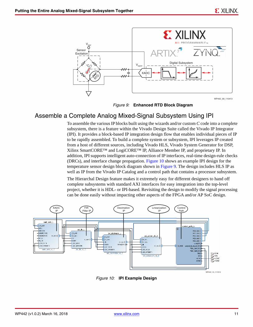
Overall, then, these improvements greatly simplify the block diagram (see Figure 9). The temperature sensor interface is realized using only a handful of passive components, which reduces BOM cost while removing error sources from the circuit. Because of Xilinx FPGA and AP SoC technology, these designs are extremely flexible, allowing designers to react to market demands extremely efficiently.
Putting the Entire Analog Mixed-Signal Subsystem Together
WP442 (v1.0.2) March 16, 2018 www.xilinx.com 11
Assemble a Complete Analog Mixed-Signal Subsystem Using IPI To assemble the various IP blocks built using the wizards and/or custom C code into a complete subsystem, there is a feature within the Vivado Design Suite called the Vivado IP Integrator (IPI). It provides a block-based IP integration design flow that enables individual pieces of IP to be rapidly assembled. To build a complete system or subsystem, IPI leverages IP created from a host of different sources, including Vivado HLS, Vivado System Generator for DSP, Xilinx SmartCORE™ and LogiCORE™ IP, Alliance Member IP, and proprietary IP. In addition, IPI supports intelligent auto-connection of IP interfaces, real-time design-rule checks (DRCs), and interface change propagation. Figure 10 shows an example IPI design for the temperature sensor design block diagram shown in Figure 9. The design includes HLS IP as well as IP from the Vivado IP Catalog and a control path that contains a processor subsystem.
The Hierarchal Design feature makes it extremely easy for different designers to hand off complete subsystems with standard AXI interfaces for easy integration into the top-level project, whether it is HDL- or IPI-based. Revisiting the design to modify the signal processing can be done easily without impacting other aspects of the FPGA and/or AP SoC design.
X-Ref Target - Figure 9
Figure 9: Enhanced RTD Block Diagram
VREF
XADC
WP442_09_110413
RTD
Sensor Excitation
°C VREFP
Digital Subsystem
X-Ref Target - Figure 10
Figure 10: IPI Example Design
WP442_10_111513
XADC IP
FIR Filter IP
Decimation IP
Linearization IP
ControlPath
12 www.xilinx.com WP442 (v1.0.2) March 16, 2018
Summary
SummaryThis white paper shows that many common analog signal-processing functions can be implemented easily and efficiently in Xilinx FPGAs and AP SoCs using built-in IP and Wizards or by using C code to design custom functions. The subsystem is created by connecting the various IP blocks/functions together in a schematic-like environment called IPI.
Furthermore, it shows that moving analog signal-processing functions into the digital domain can have a number of advantages, including reduction in BOM cost, improved accuracy, faster time to market, and increased flexibility.
These techniques and tools can be evaluated today using the Xilinx 7 series evaluation boards along with the AMS101 mezzanine card, part of the analog mixed-signal evaluation platform, which allows testing of the Xilinx analog-to-digital converter (XADC) and analog mixed-signal (AMS) technology. See xilinx.com for more information.
Further Reading and Resources1. Xilinx Backgrounder, 9 Reasons Why the Vivado Design Suite Accelerates Design Productivity
2. UG998, Introduction to FPGA Design with Vivado High-Level Synthesis
3. WP392, Xilinx Analog Mixed Signal Solutions
4. ZedBoard at http://www.zedboard.org/
5. AMS101 Evaluation Card at Xilinx website
References1. Elder, Scott: “Designing with Op-Amps Is Ending” at Planet Analog,
http://www.planetanalog.com/author.asp?section_id=526&doc_id=560151&piddl_msgpage=1#msgs
2. Smith, Steven W., Ph.D.: The Scientist and Engineer's Guide to Digital Signal Processing, Chapter 3, “ADC and DAC” at website http://www.dspguide.com/ch3/2.htm
3. Kester, Walt: Mixed-Signal and DSP Design Techniques, Section 6, “Digital Filters” at Analog Devices, http://www.analog.com/static/imported-files/seminars_webcasts/MixedSignal_Sect6.pdf
4. Leibson, Steve: “Need Another Bit or 2 of A/D Resolution?” at Programmable Planet, http://www.programmableplanet.com/author.asp?section_id=2999&doc_id=259748
5. Taranovich, Steve: “Integration Choices: Analog Filters vs. Digital Filters” at Planet Analog, http://www.planetanalog.com/author.asp?section_id=3065&doc_id=560512
6. Reference Schematic 3450: “Positive Analog Feedback Compensates PT100 Transducer” at Maxim Integrated, http://www.maximintegrated.com/app-notes/index.mvp/id/3450
7. Trump, Bruce: “Analog Linearization of Resistance Temperature Detectors” at Texas Instruments Inc., Analog Applications Journal, 4Q 2011, http://www.ti.com/lit/an/slyt442/slyt442.pdf
8. Application Note AN-709, King, Grayson and Fukushima, Toru: “RTD Interfacing and Linearization Using an ADuC8xx MicroConverter®” at Analog Devices, http://www.analog.com/static/imported-files/application_notes/AN709_0.pdf
9. Cost-Optimized Product Selection Guide, Artix®-7 FPGAs Product Table
10. Xcell Journal, Issue 68, p. 54, “Interpolated Lookup Tables: Simple Way to Implement a DSP Function”
Revision History
WP442 (v1.0.2) March 16, 2018 www.xilinx.com 13
Revision HistoryThe following table shows the revision history for this document:
DisclaimerThe information disclosed to you hereunder (the “Materials”) is provided solely for the selectionand use of Xilinx products. To the maximum extent permitted by applicable law: (1) Materials aremade available “AS IS” and with all faults, Xilinx hereby DISCLAIMS ALL WARRANTIES ANDCONDITIONS, EXPRESS, IMPLIED, OR STATUTORY, INCLUDING BUT NOT LIMITED TO WARRANTIESOF MERCHANTABILITY, NON-INFRINGEMENT, OR FITNESS FOR ANY PARTICULAR PURPOSE; and (2)Xilinx shall not be liable (whether in contract or tort, including negligence, or under any othertheory of liability) for any loss or damage of any kind or nature related to, arising under, or inconnection with, the Materials (including your use of the Materials), including for any direct,indirect, special, incidental, or consequential loss or damage (including loss of data, profits,goodwill, or any type of loss or damage suffered as a result of any action brought by a third party)even if such damage or loss was reasonably foreseeable or Xilinx had been advised of the possibilityof the same. Xilinx assumes no obligation to correct any errors contained in the Materials or tonotify you of updates to the Materials or to product specifications. You may not reproduce, modify,distribute, or publicly display the Materials without prior written consent. Certain products aresubject to the terms and conditions of Xilinx’s limited warranty, please refer to Xilinx’s Terms of Salewhich can be viewed at http://www.xilinx.com/legal.htm#tos; IP cores may be subject to warrantyand support terms contained in a license issued to you by Xilinx. Xilinx products are not designedor intended to be fail-safe or for use in any application requiring fail-safe performance; you assumesole risk and liability for use of Xilinx products in such critical applications, please refer to Xilinx’sTerms of Sale which can be viewed at http://www.xilinx.com/ legal.htm#tos.
Automotive Applications DisclaimerAUTOMOTIVE PRODUCTS (IDENTIFIED AS “XA” IN THE PART NUMBER) ARE NOT WARRANTED FORUSE IN THE DEPLOYMENT OF AIRBAGS OR FOR USE IN APPLICATIONS THAT AFFECT CONTROL OFA VEHICLE (“SAFETY APPLICATION”) UNLESS THERE IS A SAFETY CONCEPT OR REDUNDANCYFEATURE CONSISTENT WITH THE ISO 26262 AUTOMOTIVE SAFETY STANDARD (“SAFETY DESIGN”).CUSTOMER SHALL, PRIOR TO USING OR DISTRIBUTING ANY SYSTEMS THAT INCORPORATEPRODUCTS, THOROUGHLY TEST SUCH SYSTEMS FOR SAFETY PURPOSES. USE OF PRODUCTS IN ASAFETY APPLICATION WITHOUT A SAFETY DESIGN IS FULLY AT THE RISK OF CUSTOMER, SUBJECTONLY TO APPLICABLE LAWS AND REGULATIONS GOVERNING LIMITATIONS ON PRODUCTLIABILITY.
Date Version Description of Revisions
03/16/2018 1.0.2 Updated URLs.
01/18/2018 1.0.1 Typographical edits.
11/18/2013 1.0 Initial Xilinx release.