Efficient carrier multiplication in CsPbI3 perovskite nanocrystals · 2018-10-25 · ARTICLE...
10
Delft University of Technology Efficient carrier multiplication in CsPbI3 perovskite nanocrystals de Weerd, Chris; Gomez, Leyre; Capretti, Antonio; Lebrun, Delphine M.; Matsubara, Eiichi; Lin, Junhao; Ashida, Masaaki; Spoor, Frank C.M.; Siebbeles, Laurens; Houtepen, Arjan DOI 10.1038/s41467-018-06721-0 Publication date 2018 Document Version Final published version Published in Nature Communications Citation (APA) de Weerd, C., Gomez, L., Capretti, A., Lebrun, D. M., Matsubara, E., Lin, J., ... Gregorkiewicz, T. (2018). Efficient carrier multiplication in CsPbI3 perovskite nanocrystals. Nature Communications, 9(1), [4199]. https://doi.org/10.1038/s41467-018-06721-0 Important note To cite this publication, please use the final published version (if applicable). Please check the document version above. Copyright Other than for strictly personal use, it is not permitted to download, forward or distribute the text or part of it, without the consent of the author(s) and/or copyright holder(s), unless the work is under an open content license such as Creative Commons. Takedown policy Please contact us and provide details if you believe this document breaches copyrights. We will remove access to the work immediately and investigate your claim. This work is downloaded from Delft University of Technology. For technical reasons the number of authors shown on this cover page is limited to a maximum of 10.
Transcript of Efficient carrier multiplication in CsPbI3 perovskite nanocrystals · 2018-10-25 · ARTICLE...
Delft University of Technology
Efficient carrier multiplication in CsPbI3 perovskite nanocrystals
de Weerd, Chris; Gomez, Leyre; Capretti, Antonio; Lebrun, Delphine M.; Matsubara, Eiichi; Lin, Junhao;Ashida, Masaaki; Spoor, Frank C.M.; Siebbeles, Laurens; Houtepen, ArjanDOI10.1038/s41467-018-06721-0Publication date2018Document VersionFinal published versionPublished inNature Communications
Citation (APA)de Weerd, C., Gomez, L., Capretti, A., Lebrun, D. M., Matsubara, E., Lin, J., ... Gregorkiewicz, T. (2018).Efficient carrier multiplication in CsPbI3 perovskite nanocrystals. Nature Communications, 9(1), [4199].https://doi.org/10.1038/s41467-018-06721-0
Important noteTo cite this publication, please use the final published version (if applicable).Please check the document version above.
CopyrightOther than for strictly personal use, it is not permitted to download, forward or distribute the text or part of it, without the consentof the author(s) and/or copyright holder(s), unless the work is under an open content license such as Creative Commons.
Takedown policyPlease contact us and provide details if you believe this document breaches copyrights.We will remove access to the work immediately and investigate your claim.
This work is downloaded from Delft University of Technology.For technical reasons the number of authors shown on this cover page is limited to a maximum of 10.

ARTICLE
Efficient carrier multiplication in CsPbI3 perovskitenanocrystalsChris de Weerd1, Leyre Gomez1, Antonio Capretti 1, Delphine M. Lebrun2, Eiichi Matsubara3,4, Junhao Lin 5,
Masaaki Ashida4, Frank C.M. Spoor6, Laurens D.A. Siebbeles6, Arjan J. Houtepen6, Kazutomo Suenaga7,
Yasufumi Fujiwara2 & Tom Gregorkiewicz1,2
The all-inorganic perovskite nanocrystals are currently in the research spotlight owing to their
physical stability and superior optical properties—these features make them interesting for
optoelectronic and photovoltaic applications. Here, we report on the observation of highly
efficient carrier multiplication in colloidal CsPbI3 nanocrystals prepared by a hot-injection
method. The carrier multiplication process counteracts thermalization of hot carriers and as
such provides the potential to increase the conversion efficiency of solar cells. We demon-
strate that carrier multiplication commences at the threshold excitation energy near the
energy conservation limit of twice the band gap, and has step-like characteristics with an
extremely high quantum yield of up to 98%. Using ultrahigh temporal resolution, we show
that carrier multiplication induces a longer build-up of the free carrier concentration, thus
providing important insights into the physical mechanism responsible for this phenomenon.
The evidence is obtained using three independent experimental approaches, and is
conclusive.
DOI: 10.1038/s41467-018-06721-0 OPEN
1 Institute of Physics, University of Amsterdam, Science Park 904, 1098 XH Amsterdam, The Netherlands. 2 Division of Materials and Manufacturing Science,Graduate School of Engineering, Osaka University, 2-1 Yamadaoka, Suita, Osaka 565-0871, Japan. 3 Department of Physics, Osaka Dental University, 8-1Kuzuha-Hanazono, Hirakata, Osaka 573-1121, Japan. 4 Graduate School of Engineering Science, Osaka University, 1-3 Machikaneyama, Toyonaka, Osaka560-8531, Japan. 5 Department of Physics, Southern University of Science and Technology, Shenzhen 518055, China. 6 Faculty of Applied Sciences, DelftUniversity of Technology building 58, van der Maasweg 9, 2629 HZ Delft, The Netherlands. 7 National Institute of Advanced Industrial Science andTechnology (AIST), AIST Central 5, Tsukuba 305-8565, Japan. These authors contributed equally: Chris de Weerd, Leyre Gomez. Correspondence andrequests for materials should be addressed to C.W. (email: [email protected]) or to T.G. (email: [email protected])
NATURE COMMUNICATIONS | (2018) 9:4199 | DOI: 10.1038/s41467-018-06721-0 |www.nature.com/naturecommunications 1
1234
5678
90():,;

In the process of photoexcitation of a semiconductor, anelectron in the conduction band and a hole in the valence bandare created, forming an electron–hole (e–h) pair. The photo-
generated e–h pair possesses typically an excess energy, equal tothe difference between the band gap value of the material and theabsorbed photon energy. The hot electron and hole may lose theirexcess energy by cooling to the band edge by phonon scattering.However, if the excess energy reaches a certain threshold, aninteraction between a hot electron (hole) and other valenceelectrons (holes) can take place instead, such that a second e–hpair is generated. In bulk semiconductors, this phenomenon isknown as impact ionization1,2 and was first observed in crystal-line bulk semiconductors Si and Ge3. In the case of semi-conductor nanocrystals (NCs), impact ionization is more oftenreferred to as multiple exciton generation or carrier multi-plication (CM), and its probability can be enhanced. CM isaccompanied by Auger recombination (AR), which is the reverseprocess of impact ionization4: an e–h pair can recombine, givingup its energy to another electron or hole, thus increasing itsexcess energy and creating a hot carrier. Sequential CM and ARcan continue until the hot e–h pair has cooled below the CMthreshold, e.g., by phonon scattering.
In the last two decades, semiconductor NCs have been widelyinvestigated for their size-tunable properties. As the NC sizedecreases and approaches the Bohr radius of the particularmaterial, quantum confinement sets in. As such, the nanoparticledimensions, and not the e–h Coulomb coupling strength, definesthe exciton spatial confinement. Upon confinement, the wavefunctions of the electron and hole are modified and eventuallydiscrete energy levels replace the continuous energy bands of thebulk material, while the band gap increases5,6. Because of thestrong confinement, carrier–carrier Coulomb interactions areenhanced which can give priority to decay via AR, and reversibly,to efficient CM by hot carriers7–9. Employing CM for photo-voltaic devices has already proved its benefit and usefulness10. Inparticular, a photovoltaic power conversion efficiency up to ~44%is expected for cells that make optimal use of CM11,12, surpassingthe well-known Shockley–Queisser limit of ~33%13. Indeed, anexternal photocurrent quantum efficiency (the ratio of photo-carriers collected by an external circuit to the number of incidentphotons) exceeding 100% has been reported10. Previously, CMhas been demonstrated in many semiconductor (nano)structures,e.g., PbSe, PbS, CdSe, Si, Ge and graphene10–12,14–30, as reviewedby Smith and Binks31. Until now, however, CM has not beenreported for perovskites. These materials are at the momentintensively researched for numerous applications. Perovskitesattract considerable attention because of their outstanding opticaland electrical properties, defect tolerance and low productioncosts32–37. Recently, the all-inorganic perovskite NCs (IP-NCs)are of interest, featuring extremely efficient emission38,39 andfast radiative recombination40. They combine the advantagesof perovskites and NCs and, being free from the organic com-ponent, offer better stability than the more popular hybridorganic–inorganic perovskites39. Moreover, due to the recentdemonstration of a stable solar cell based on CsPbI3 NCs41,this material has changed its status from being a scientific curi-osity to a highly promising new alternative for perovskite-basedapplications.
In the case of IP-NCs, CM would be of great fundamentalimpact on this upcoming material and directly beneficial to itsapplication in novel optoelectronic nanodevices, most notablyphotodetectors, while the band gaps of the currently available IP-NCs are still too large for practical impact in solar cells. Never-theless, the research continues vigorously and rapid progress isbeing made—see, e.g., ref42 for a very recent report on the pos-sibility of multiple exciton generation in CsPbBr3 upon nonlinear
absorption at sub-band energies. That is why CM in IP-NCs is ofinterest and has been investigated further. Previous researchconducted on IP-NCs NCs, failed to reveal CM: comparison of PLdecay dynamics upon excitation with high (hν > 2Egap) and low(hν < 2Egap) energy photons did not show any signatures of CM43.
Here, we report on the observation of efficient CM in a col-loidal dispersion of CsPbI3 NCs, with a band gap energy of 1.78eV. We explicitly demonstrate the CM effect using ultrafasttransient absorption (TA) spectroscopy in a variety of experi-mental approaches. By comparing carrier transients at differentpump photon energies, we demonstrate the fingerprint of CM inthe form of a fast component induced by AR of multiple e–h pairsappearing in the same NC. The observation is made both for theinduced absorption and induced bleach. We confirm the CMeffect and evaluate its efficiency by measuring the carrier gen-eration rate as a function of excitation energy. We find an effi-ciency of 98 and 97% as extracted from the photo-induced bleach(PIB) and photo-induced absorption (PIA) dynamics respectively.In addition, we investigate in detail the dynamics for abovethreshold pumping, on a picosecond time scale. This reveals thatthe CM process coincides with a longer build-up of the freecarrier concentration and provides new and important insightsinto the CM phenomenon. Moreover, we reproduce our investi-gations at an independent experimental setup, with somewhatdifferent characteristics, and on newly synthesized materials. Inthat way, we provide an unambiguous evidence of CM in all-inorganic CsPbI3 NCs.
ResultsSynthesis and microscopic characterization. The CsPbI3 NCswere synthesized by a wet-chemistry method, following theslightly modified protocol described in refs39 and 41. We used asynthesis temperature of 180 °C in order to steer the productiontowards NCs with a small band gap energy, i.e., larger size.Moreover, large NCs have a larger absorption cross section, andtherefore are excited preferentially. We measured a photo-luminescence quantum yield (PL QY) of 42.4 ± 7 % at excitationof energy of 3.1 eV (400 nm, see Supplementary Fig. 1 for theexcitation dependent PL QY), which is similar to previouslyreported values39,41, and is expected for NCs with a large size (theBohr radius is ~6 nm for this material therefore the NCs are inthe weak confinement regime). The structural characteristics ofthe NCs were determined using a state-of-the-art low-voltagemonochromatic scanning transmission electron microscope(STEM) with a spatial resolution below 1.6 Å. Figure 1a shows theannular dark field STEM image of the drop-casted NCs with anaverage size of 11.5 ± 0.6 nm (see also Supplementary Fig. 2 anddetailed information in the Supplementary Information onmaterials and methods). A high-resolution annular dark fieldimage of a 12 nm NC is shown in Fig. 1b. Here, the (nearly) cubicarrangement of the atoms is clearly observed, consistent with theperovskite structure. This is further analyzed by simultaneouslyperforming energy dispersive X-ray spectroscopy (Fig. 1c) forelemental identification and core-loss electron energy loss spec-troscopy (EELS, Fig. 1d). Mainly Cs, Pb and I are detected and theAu signal arises from the reflection of the TEM grid. The Cs:Pb:Iratio, determined from the quantification of the energy dispersiveX-ray signal under the L-lines of the corresponding elements, is1:1:3 ± 10%, confirming that (mostly) NCs of CsPbI3 perovskitehave been formed. At high losses, two distinctive peaks at 733 eVand 746 eV are observed, corresponding to CsM4.5, and thebroader peak at 700 eV which corresponds to the delayed featureof the IM4.5 ionization edge. To determine the band gap of a singleNC, imaging and valence-loss EELS collections were performed inparallel, with a high energy resolution (zero loss peak of
ARTICLE NATURE COMMUNICATIONS | DOI: 10.1038/s41467-018-06721-0
2 NATURE COMMUNICATIONS | (2018) 9:4199 | DOI: 10.1038/s41467-018-06721-0 | www.nature.com/naturecommunications
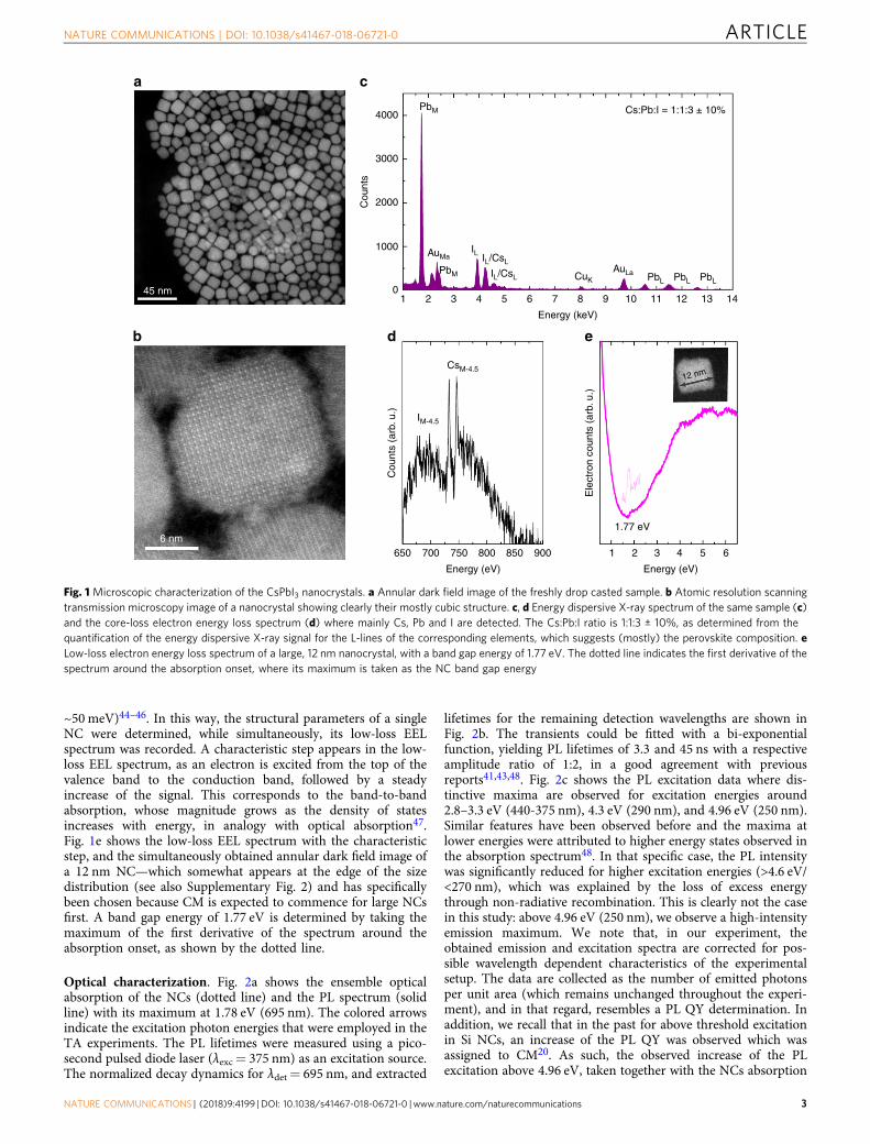
~50meV)44–46. In this way, the structural parameters of a singleNC were determined, while simultaneously, its low-loss EELspectrum was recorded. A characteristic step appears in the low-loss EEL spectrum, as an electron is excited from the top of thevalence band to the conduction band, followed by a steadyincrease of the signal. This corresponds to the band-to-bandabsorption, whose magnitude grows as the density of statesincreases with energy, in analogy with optical absorption47.Fig. 1e shows the low-loss EEL spectrum with the characteristicstep, and the simultaneously obtained annular dark field image ofa 12 nm NC—which somewhat appears at the edge of the sizedistribution (see also Supplementary Fig. 2) and has specificallybeen chosen because CM is expected to commence for large NCsfirst. A band gap energy of 1.77 eV is determined by taking themaximum of the first derivative of the spectrum around theabsorption onset, as shown by the dotted line.
Optical characterization. Fig. 2a shows the ensemble opticalabsorption of the NCs (dotted line) and the PL spectrum (solidline) with its maximum at 1.78 eV (695 nm). The colored arrowsindicate the excitation photon energies that were employed in theTA experiments. The PL lifetimes were measured using a pico-second pulsed diode laser (λexc= 375 nm) as an excitation source.The normalized decay dynamics for λdet= 695 nm, and extracted
lifetimes for the remaining detection wavelengths are shown inFig. 2b. The transients could be fitted with a bi-exponentialfunction, yielding PL lifetimes of 3.3 and 45 ns with a respectiveamplitude ratio of 1:2, in a good agreement with previousreports41,43,48. Fig. 2c shows the PL excitation data where dis-tinctive maxima are observed for excitation energies around2.8–3.3 eV (440-375 nm), 4.3 eV (290 nm), and 4.96 eV (250 nm).Similar features have been observed before and the maxima atlower energies were attributed to higher energy states observed inthe absorption spectrum48. In that specific case, the PL intensitywas significantly reduced for higher excitation energies (>4.6 eV/<270 nm), which was explained by the loss of excess energythrough non-radiative recombination. This is clearly not the casein this study: above 4.96 eV (250 nm), we observe a high-intensityemission maximum. We note that, in our experiment, theobtained emission and excitation spectra are corrected for pos-sible wavelength dependent characteristics of the experimentalsetup. The data are collected as the number of emitted photonsper unit area (which remains unchanged throughout the experi-ment), and in that regard, resembles a PL QY determination. Inaddition, we recall that in the past for above threshold excitationin Si NCs, an increase of the PL QY was observed which wasassigned to CM20. As such, the observed increase of the PLexcitation above 4.96 eV, taken together with the NCs absorption
650 750 850700 800
Energy (eV) Energy (eV)
1.77 eV
12 nm
IM-4.5
CsM-4.5
AuMa
CuK
Cs:Pb:I = 1:1:3 ± 10%
AuLa PbL
PbM
PbL PbLPbM
IL IL/CsL
IL/CsL
Ele
ctro
n co
unts
(ar
b. u
.)
Cou
nts
(arb
. u.)
Cou
nts
45 nm
6 nm900 1 2 3 4 5 6
Energy (keV)
10
1000
2000
3000
4000
ca
b d e
2 3 4 5 6 7 8 9 10 11 12 13 14
Fig. 1 Microscopic characterization of the CsPbI3 nanocrystals. a Annular dark field image of the freshly drop casted sample. b Atomic resolution scanningtransmission microscopy image of a nanocrystal showing clearly their mostly cubic structure. c, d Energy dispersive X-ray spectrum of the same sample (c)and the core-loss electron energy loss spectrum (d) where mainly Cs, Pb and I are detected. The Cs:Pb:I ratio is 1:1:3 ± 10%, as determined from thequantification of the energy dispersive X-ray signal for the L-lines of the corresponding elements, which suggests (mostly) the perovskite composition. eLow-loss electron energy loss spectrum of a large, 12 nm nanocrystal, with a band gap energy of 1.77 eV. The dotted line indicates the first derivative of thespectrum around the absorption onset, where its maximum is taken as the NC band gap energy
NATURE COMMUNICATIONS | DOI: 10.1038/s41467-018-06721-0 ARTICLE
NATURE COMMUNICATIONS | (2018) 9:4199 | DOI: 10.1038/s41467-018-06721-0 |www.nature.com/naturecommunications 3

spectrum (Fig. 2a), suggests an increase in PL QY appearing dueto CM20. Unfortunately, an observation of this phenomenon atstill higher excitation energies was not possible due to limitationsof the setup.
Transient absorption spectroscopy. The peculiarity of the PLexcitation spectrum in Fig. 2c motivated the use of TA spectro-scopy, which in the past has proved very successful in CMinvestigation in nanostructures15,16,21,49. For direct band gapsemiconductors, the interband PIB is often used to study the CMprocess, while for indirect band gap semiconductors this istypically weak, therefore it is easier to monitor the PIA, caused byintra-band transitions of (free) carriers generated by the pumppulse. First, a strong pump pulse provides band-to-band excita-tion, which in NCs leads to generation of e–h pairs. After pho-toexcitation, these initially hot e–h pairs relax and bleach theoptical absorption at the band edge. A second, weaker pulseprobes the carrier concentration as a function of the pump–probedelay time. As a result, the transmittance for photons with energynear the (direct) band gap increases, and yields a negative PIBsignal. The TA signal is defined as the difference of the absor-bance or optical density (OD) with and without pump and isobtained as
ΔODðt; λÞ ¼ log10IprobeðλÞ
IpumpþprobeðλÞ; ð1Þ
where Iprobe(λ) and Ipump+probe (λ)′ are the transmitted probefluences with the pump pulse off and on, respectively. Twoapproaches are generally considered: firstly the A/B methodapplied by Schaller et al. relying on the appearance of a fastcomponent in the transient as the pump energy exceeds the CMthreshold50, and secondly the excitation energy dependence of thenumber of generated carriers (i.e., carrier generation yield),determined by the PIB or PIA amplitude as a function of theabsorbed photon fluence15,16,51,52. Here, we apply both methods,yielding consistent results. We also consider both the PIB as wellas PIA dynamics, whose results are in agreement with each other.In addition, since ultrafast spectroscopy setups often have theirown characteristics and elements, we repeated our investigationsat two different experimental stations (see the Methods sectionforthe details of the setups used to obtain the presented data). Ourapproach (using multiple methods to identify CM and repeating
the experiments at two stations) is unique, and was followedbecause of the great experimental difficulty of (ultrafast) CMexperiments, which are prone to artefacts, as evidenced by theexisting literature see, e.g., ref15.
The fingerprint of CM. Fig. 3 shows the transient PIB measuredaround its maximum at λprobe= 680 nm (obtained by integratingthe signal between 675 and 685 nm). Here, the results for twoexcitation wavelengths are compared: below and above the CMthreshold, at λexc= 500 nm (1.4Egap, Fig. 3a) and λexc= 295 nm(2.4Egap, Fig. 3b), respectively (see Supplementary Fig. 3 for alltransient PIB dynamics measured in this study). While per-forming our TA measurements, we have maintained the numberof absorbed photons per NC at a very low level (⟨Nexc⟩« 1) withinthe so-called linear regime. This is confirmed by the fact that theinitial amplitude A of the TA dynamics grows linearly with theabsorbed photon fluence (orange dots in the insets of Fig. 3a, b),and particularly by the ratio between the initial amplitude A andthe tail amplitude B (A/B) which remains invariant within theinvestigated absorbed photon fluence range (turquoise dots).Specifically, from the latter observation, multi-photon absorptioncan be completely excluded. As such, the observed fluenceincrease in this range yields only a higher number of excited NCswhile maintaining ⟨Nexc⟩« 1: under these excitation conditionseach NC contains at most 1 e–h pair, following absorption of asingle photon.
Considering both excitation energies, we note that the behaviorof the transient PIB signal is remarkably different: in both casesthe dynamics show a tail with a relaxation time which fits thedisplayed time window (500 ps). However, for the UV excitation,an additional fast component appears. This is commonly taken asa fingerprint of CM, which we will now briefly explain. Here, wefollow the reasoning as originally proposed by Schaller et al.50.which has been employed in many studies of CM before15,21—and see also ref27. A hot carrier can induce CM, if its excessenergy is greater than the threshold energy, which must at least beequal to the NC band gap. A single photo-generated hot e–h pairloses its excess energy by generating an additional e–h pair. Thishigher exciton multiplicity causes the amplitude increase of thePIB/PIA signal at the short time scale. Subsequently, the multipleexcitons localized within the same NC decay through AR. Thisprocess typically occurs within 10-100 ps and gives rise tothe initial fast component in the measured dynamics53. The
4.130.5
a b c
0.4
0.3
0.2
0.1
0.0300 400 500
Wavelength (nm) Time (ns)
�1 = 3.3 ns�2 = 45 ns
Abs
orba
nce
PL intensity (arb. u.)
PL
lifet
ime
(ns)
PL lifetim
e (ns)
PL intensity(#phot. cm–2):
Nor
m. P
L in
tens
ity (
arb.
u.)
600 700 800 0 50 100 200 640250
350
450
550
600 2.070224090117120
150
125135
2.25
2.48
2.76
3.10
3.54
4.13
4.96
300
400
500
740720660 680
1.82
Emission energy (eV)
Excitation energy (eV
)
1.881.94 1.77 1.72 1.68
Emission wavelength (nm)
Exc
itatio
n w
avel
engt
h (n
m)
700150
3.10 2.48
Energy (eV)
2.07 1.77 1.55
1.012
60
40
20
0
8
4
0670 680 690
Detection wavelength (nm)700 710
0.8
0.6
0.4
0.2
0.0
Fig. 2 Optical characterization. a Absorbance (dotted) and PL (solid) spectra. The colored arrows indicate the photon energies used in the transientabsorption experiment. b Time-resolved photoluminescence (PL) measurement for λdet= 695 nm which was fitted using a bi-exponential function andyielding decay times τ1 = 3.3 ns and τ2= 45 ns. The inset shows the obtained lifetimes for all detection wavelengths. The PL lifetimes with correspondingamplitudes are shown in the inset. The uncertainty is determined by the statistical error from the fitting method. c 2D contour plot of the PL excitation,showing the effect of excitation energy on the PL emission and intensity. A PL maximum is observed around <250 nm (>4.96 eV), which could bethe first sign of carrier multiplication. The excitation and emission intensities are corrected for the wavelength dependent components of the setupand spectral sensitivity
ARTICLE NATURE COMMUNICATIONS | DOI: 10.1038/s41467-018-06721-0
4 NATURE COMMUNICATIONS | (2018) 9:4199 | DOI: 10.1038/s41467-018-06721-0 | www.nature.com/naturecommunications

experimental data shown in Fig. 3 could be fitted with a doubleand triple exponential function for below and above CMthreshold pumping respectively. This yields τ1= ~ 89 ps for thefast component for above threshold pumping which agrees withpreviously reported time constants for the AR process43,53,54.After the multi-exciton relaxation process, a single excitonremains, which decays through non-radiative and radiativerecombination processes, depending on the characteristics ofindividual NCs, (because the ensemble PL QY < 100%) giving riseto the slow decay. The experimentally found slow decay timeconstants are τ2= ~190-200 ps and τ3=~3300 ps (see alsoSupplementary Fig. 4), where the latter agrees with the radiativelifetime determined from the TR-PL measurements.
To prove that the initial fast component is indeed due to AR,we show that it can be reproduced by increasing the pumpfluence at below-threshold pump photon energy, such thatmulti-photon absorption occurs. Figure 3c shows the transientsfor the highest pump fluences in the linear regime (solid lines)which can be reached, at far below (1.2Egap, purple), just above(2.2Egap, orange), and above (2.4Egap, black) CM thresholdexcitation. The dynamics are normalized to the same B valuesuch that the increase of the fast component can clearly bedistinguished. Then, the pump fluence for the below-thresholdexcitation at 1.2Egap is increased, until its initial amplitude Amatches that of the transient obtained for the above-thresholdexcitation at 2.2Egap in the linear regime. And similarly, thepump fluence at 2.2Egap is increased until it reaches A forexciting at 2.4Egap in the linear regime (dotted lines). It can
clearly be seen that the transients obtained under these twoexcitation conditions (in- and outside the linear regime) arepractically identical, which confirms that the initial fastcomponent is induced by AR: the decay through AR of multiplee–h pairs induced by multi-photon absorption and by CM, hasidentical characteristics, as was anticipated.
CM efficiency. Having obtained the fingerprint of CM, we nowstudy its dependence on the pump fluence and excitation energy.The initial amplitude A serves as a measure for the number ofgenerated e–h pairs and is therefore directly associated with theCM efficiency. Following the approach of Beard et al.55, ΔA isrelated to the CM QY via:
ΔA ¼ QYFabs; ð2Þ
where Fabs is the absorbed photon fluence. For each excitationwavelength and corresponding pump power, Fabs is calculated via
Fabs ¼PpumpλODðλpumpÞ
f; ð3Þ
where Ppump is the pump power at the sample position andcorrected for a possible mismatch in pump/probe overlappingarea; λ is the excitation wavelength; OD(λpump) is the opticaldensity determined from the linear absorption measurementand f is the laser frequency, which is setup specifically. As hasbeen demonstrated in Fig. 3a and b, ΔA has a linear functionpassing through the origin and it follows from equation (2) that
B (hν)
A (hν)
A (hν)
B (hν)
B (hν)
A (hν)
ba
–0.80.009 μJ/cm2
0.004 μJ/cm2
0.003 μJ/cm2
–0.6
�A
(m
OD
)
–0.4
–0.2
0.0
0.00.0 0.5
Fluence ×1012 absorbed photons cm–21.0
2
4
6
A/B
0.2
0.4
0.6
A (
mO
D)
A (
mO
D)
0.8
1.0
0 100 200 300
Delay time (ps)
Linear regime: Nonlinear regime:1.2Egap
2.2Egap
1.2Egap
2.2Egap
2.4Egap
Delay time (ps)
400 500
0 50 100 150 200 250 300 350 450400
–0.80.081 μJ/cm2
0.053 μJ/cm2
0.033 μJ/cm2
–0.6�
A (
mO
D)
–0.4
–0.2
0.0
c
–0.8
–1.0
–0.6
Nor
mal
ized
�A
(m
OD
)
–0.4
–0.2
0.0
0.00.0 0.5 1.0 1.5
Fluence ×1012 absorbed photons cm–22.0
2
4
6
8
10
A/B
0.2
0.1
0.30.4
0.6
0.5
0 100 200 300
Delay time (ps)
400 500
Fig. 3 Transient absorption dynamics. a, b Dynamics below (a) and above (b) the carrier multiplication (CM) threshold, i.e., at pump wavelengths of 500nm (2.48 eV) and 295 nm (4.2 eV), respectively. The dashed lines represent the exponential fit to the data. The appearance of the additional fastcomponent when pumping at 4.2 eV is the fingerprint of CM. The insets shows the initial transient amplitude A and its ratio to the single exciton decay tailA/B, as a function of the absorbed photon fluence, demonstrating the single photon absorption (linear) regime. All dynamics are measured at probewavelengths around the photo-induced bleach maximum (680 nm) by integrating the signal from 675 to 685 nm. The latter determines the error bars inthe y-direction. The error in the x-direction arises from small fluctuations in the pump power. c Linear vs. nonlinear regime, showing the decay throughAuger recombination with pumping outside the linear regime (i.e., by multi-photon absorption) and through CM, yields the same dynamics
NATURE COMMUNICATIONS | DOI: 10.1038/s41467-018-06721-0 ARTICLE
NATURE COMMUNICATIONS | (2018) 9:4199 | DOI: 10.1038/s41467-018-06721-0 |www.nature.com/naturecommunications 5

its slope determines the carrier generation yield. Accordingly,Fig. 4a shows ΔA as a function of Fabs. At each pump energy,this value is determined for all pump fluences in the linearregime (as previously explained, the linear regime is mainlyconfirmed through invariance of the A/B ratio of the decaytransients). Without multiple carrier generation, i.e., below theCM threshold, this slope should remain constant for differentpump energies, which is indeed the case. In Fig. 4a the pinkdata points correspond to the pump energies Eexc < 2.75 eV <2Egap and follow the same linearity, which subsequentlydetermines the QY= 1 line. From this it follows that QY= 2 isdetermined by a doubling of ΔA at equal fluence. In that way,the slope of the linear function through ΔA for each specificpump energy is a measure for the QY efficiency. Note that inFig. 4a the slope gradually increases for pump energies abovethe CM threshold, i.e., Eexc ≥ 3.54 eV ≥ 2Egap, rather thanjumping to the QY= 2 position (blue and turquoise curves).This is among others a result of the NC size distribution onCM, which commences first for the large NCs, with a smallerband gap energy. We find that at 4.0–4.2 eV excitation (2.2–2.4Egap) the ΔA lines approach QY= 2 (dark yellow and black).The error bars in the y-direction are determined by the aver-aging between t= 4–8 ps after photo-excitation, to extract ΔA.In the x-direction, the error is determined by the upper andlower values of the measured pump power in between con-secutive measurements.
ΔA in Fig. 4a only takes into account the initial amplitude A asa measure for the number of e–h pairs. However, to determinethe exact QY value, their multiplicity should be normalized to theB value since our transients do not decay to zero within theavailable time window. In that way, the experimental CM yield φ(hν) can be determined from the A/B ratio at a specific energyEexc > 2Egap, scaled to the value corresponding to below CMthreshold pumping, via
φðhνÞ ¼ A hνð Þ=BðhνÞA 1:2Egap� �
=Bð1:2EgapÞ: ð4Þ
Figure 4b shows φ(hν) as a function of the pump energynormalized to the NCs band gap energy of 1.78 eV. In that way,an increase of the QY can be easily monitored and can start from2, which is indeed what we observe. Here, a direct determinationof the CM efficiency (ηCM) can be made, following the modelproposed in ref.55:
CMQY ¼ hνEgap
� 1
!ηCM; ð5Þ
where hν is the incident pump photon energy. The characteristicstep-like feature with its threshold energy at 2Egap is obtained for
3.0a b
c
2.2PIB
4.20 eV 4.00 eV
3.88 eV 3.54 eV
2.75 eV
2.25 eV
3.10 eV
2.48 eV
150 fs pulse
�=1
�=0.2
�=0.99
�=0.98
�=0.
97
�=0.9
�=0.8
�=0.5
PIA2.0
1.8
1.6
1.4
1.2
1.0
4.2 eV QY = 3
QY = 2
QY = 1
4.0 eV3.88 eV3.54 eV<2.75 eV
Eexc:
2.5
2.0
�A
max
(m
OD
)N
orm
aliz
ed �
A (
mO
D)
Qua
ntum
yie
ld
1.5
1.0
0.5
0.0
–1.0
–0.8
–0.6
–0.4
–0.2
0.0
0.0
–1 0 1 2 3 4 5 6
0.5 1.0 1.5
Fluence (×1012 absorbed photons cm–2)
Delay time (ps)
2.0 2.5 3.0 3.5 1.0 1.5 2.0
h�/Egap
2.5 3.0
Fig. 4 Carrier multiplication efficiency and Auger recombination. a ΔA as a function of the absorbed photon fluence. The solid lines represent a linear fitthrough the data points. b CM efficiency plotted as a function of excitation energy normalized to the band gap energy of the CsPbI3 nanocrystals. The blueand pink data points correspond to the yield calculated from the A/B ratios deduced from the photo-induced-bleach and -absorption respectively. c Initialrise of the photo-induced bleach signal (normalized) which becomes slower when the nanocrystals are excited with higher photon energies, and carriermultiplication sets in. The error bars are determined by small fluctuations in the pump power (x-direction) and from integrating the dynamics between 4and 8 ps yielding an upper and lower limit for ΔA (y-direction)
ARTICLE NATURE COMMUNICATIONS | DOI: 10.1038/s41467-018-06721-0
6 NATURE COMMUNICATIONS | (2018) 9:4199 | DOI: 10.1038/s41467-018-06721-0 | www.nature.com/naturecommunications

ηCM= 1. Subsequently, as the conversion efficiency decreases, thesharp onset broadens as is indicated by the dotted lines. Here, weobtain a high CM conversion efficiency ηCM of ~98% and ~97%,as deduced from the dynamics around the PIB as well as the PIAmaxima (see also Supplementary Figs. 5 and 6 for PIA dynamicsand TA spectra respectively).
Photo-bleach rise time. Now we consider the rise time of thePIB transients as a function of the excitation energy, whichevidences the build-up of the free carrier population (Fig. 4c).Here, an abrupt increase appears when the CM thresholdidentified from our above discussed measurements, is reached—i.e., Eexc ≥ 2Egap. This delay in rise time is clearly longer thanthe experimental temporal resolution of the setup (see alsoSupplementary Fig. 7). It can be observed for the PIB as well asthe PIA (see Supplementary Fig. 8), on a similar time scale. Itscharacteristic time constant is estimated as 1–3 ps, dependingon the pump energy, in agreement with ref49. One could arguethat the increase of the PIB signal build-up at higher excitationenergies, could alternatively be explained by the larger excessenergy of the photoexcited carriers and, consequently, thelonger relaxation time necessary to reach the band edge statesprobed by the PIB56. However, such a possibility is at variancewith firstly the observation that the effect is also visible forPIA, which probes all the carriers in the band, and secondlythe persistence of the rapid increase of the signal rise, forexcitation above the CM threshold. We therefore—tentatively—attribute this additional e–h pair generation time to the CMprocess.
DiscussionThe presented experimental results provide new and uniqueinsights into the physical mechanism of the CM process. WhileCM has been investigated and modeled theoretically for sometime now, no generally accepted model of its physicalmechanism exists. In particular, very little is known on thematerial parameters governing the efficiency and the thresholdof CM—the most important features determining the possibleimpact of CM for practical applications. The current observa-tion provides here two important clues. First: the CM process isnot instantaneous, the additional carriers appear clearly afterthose generated primarily upon photon absorption. And sec-ond: CM seemingly does not affect the initial increase of thePIB signal (the first 150 fs), which, depending on the pumpenergy is determined by a combination of carrier generationupon photon absorption and their cooling to the probed state56.The latter observation is especially insightful: since theexperimentally observed cooling time is determined only by therelaxation between the lowest states in bands, this implies thatthe hot carrier losing its energy by CM is not directly trans-ferred to the lowest state, and that the secondary carrier, createdby CM, arrives in a state with a considerably longer relaxationtime. We recall that such states (in the form of self-trappedexcitons) have been investigated in the past for Si NCs57–59 andhave recently been invoked also for IP-NCs60. We have alsoobserved that the time constant of this very characteristicprolonged build-up of PIB signal depends on the NC size,shortening for smaller NCs—see Supplementary Fig. 9. Such adependence has indeed been postulated by some theoreticalmodels of CM61. Moreover, we have shown that the enhance-ment of the rise time is uniquely related to the onset of CM, anddoes not appear when multiple electron–hole pairs are gener-ated by high-power subthreshold pumping—see SupplementaryFig. 10.
Finally we briefly address the possible origin of the differentoutcome of this study in comparison with the previous inves-tigation43. In our opinion, this could be related to small dif-ferences in the material preparation. The synthesis of IP-NCshas been reported only in 201539 and while the protocol is notvery complicated, a quick literature scan readily reveals thatproperties of materials prepared by different groups are notidentical. In the present case, one specific difference could bethe local stoichiometry, especially close to the surface, and apossible formation of insulating inclusions, featuring strongabsorption bands in the 3.5–4 eV range—this in analogy to therecently identified CsPbBr3/Cs4PbBr6 hybrids62. One couldspeculate that strong absorption at energies close to twice theband gap could promote CM13. One other important differenceof the present study is the application of PIA/PIB rather thanultrafast PL spectroscopy, as used in ref43. It cannot be excludedthat both techniques could probe different populations of car-riers, with PL reflecting exclusively a population of the emittingstate. In conclusion, we demonstrate efficient CM in CsPbI3NCs from the transient PIB and PIA dynamics in TA spec-troscopy, using a variety of experimental strategies. Theoccurrence of CM is identified through the observation of anadditional fast component in the transient dynamics, recordedfor above-threshold pumping, maintaining the experimentalconditions ⟨Nexc⟩ « 1. CM is further confirmed from the photo-excitation energy dependence of carrier generation yield as afunction of pump fluence. CM commences just after the energyconserving threshold of Eexc ≥ 2Egap of the large NC fraction(dNC ~ 12 nm with Egap= 1.77 eV) and features a CM QY up to98%. In addition, coincident with the CM process a longerpicosecond build-up of the free carrier concentration for high-energy pumping is observed.
MethodsMaterials. The CsPbI3 NCs were synthesized following the protocol firstreported by Protesescu et al. in 2015, applying a slight alteration39. To preparethe Cs-oleate, 0.814 g of Cs2CO3 is mixed with 40 mL of ODE and 2.5 mL of OA.The mixture is subsequently stirred at 150 °C in an inert atmosphere until thereaction is complete. Here, the reactants are dried for 1 h at 120 °C. Toinduce the formation of NCs, 5 mL of ODE and 0.188 mmol of PbI2 are dried ina N2 atmosphere for 1 h at 120 °C. After water removal, 0.5 mL of dried OA and0.5 mL of dried OLA are added to the reaction flask, increasing the temperatureto 180 °C. After the solvation of the PbI2 is complete, 0.4 mL of the Cs-oleatesolution is injected (which is warmed up previously). The reaction takes a fewseconds where after the NCs solution is cooled down quickly using an icebath. The final product is purified using several centrifugation steps and isredispersed in hexane. The sample is diluted to reach the appropriate opticaldensity («1 OD) for the spectroscopy experiments, and transferred to a quartzcuvette (UV grade).
Experimental setups. In the TA experiment for UV pump energies (station 1,>4 eV), a Mai Tai-SP (Mountain View, U.S.A.) Diode-Pumped, Mode-Locked Ti:sapphire Laser, operating at 1 kHz with~100 fs pulse width and ~3mJ pulseenergy for an output wavelength of 800 nm, is used as the coherent light source.A frequency regulator reduces the output frequency to 200 Hz. A beam splitter isused to separate the beam to generate the pump and probe pulses. An OpticalParametric Amplifier, TOPAS-C (Light Conversion, Vilnius, Lithuania) incombination with a BBO crystal, generates the desired pump energy. The pumpbeam is subsequently guided through a delay stage (SGSP 26-200). The probesignal consists of white light which is generated using a sapphire crystal, and isspectrally resolved before reaching the detector: a 0.5 m Imaging Triple GratingSpectrogram, SpectraPro 2500i (Acton Research Corporation, Acton, U.S.A.)and an air-cooled CCD camera, PIXIS 256 (Princeton Instruments, Trenton, U.S.A.) were used. For the remaining pump energies (station 2, <4 eV), the sampleis excited with a ∼150 fs laser pulse (Light Conversion Pharos-SP operating at2.5 kHz, combined with an Orpheus OPA) and probed using a multichanneldetection of visible/near-infrared (500–800 nm) probe pulses (UltrafastSystems Helios). The broad band (white light) probe pulses are generated bya sapphire crystal using the 1030 nm pump light. We note that the experimentsat ‘low’ pump energies have been repeated at station 1 and subsequentlycompared. Those experiments yield equal dynamics and as such, validatesthe results (see Supplementary Fig. 11). The TA signal is defined as the
NATURE COMMUNICATIONS | DOI: 10.1038/s41467-018-06721-0 ARTICLE
NATURE COMMUNICATIONS | (2018) 9:4199 | DOI: 10.1038/s41467-018-06721-0 |www.nature.com/naturecommunications 7

difference of the optical density (OD) of the excited state and the ground stateand is obtained as
OD ¼ log10Itotal incident lightItransmitted light
!ð6Þ
¼ ΔOD ¼ ODpumpþprobe � ODprobe ð7Þ
¼ log10Itotal
Ipumpþprobe
!� log10
ItotalIprobe
!ð8Þ
¼ log10Itotal ´ Iprobe
Ipumpþprobe ´ Itotal
!ð9Þ
¼ log10Iprobe
Ipumpþprobe; ð10Þ
i.e.,
ΔODðt; λÞ ¼ log10Ioff ðλÞIonðλÞ
; ð11Þ
where Ioff(λ) and Ion(λ) are the transmitted probe fluences with the pump pulseoff or on, respectively. While performing the TA experiments, the colloidalsample could be stirred to avoid potential charging, although, the stirring of thesample did not induce any difference in the measured dynamics.
A LAMBDA 950 UV/VIS/NIR spectrophotometer, PerkinElmer, is used tomeasure the absorbance/optical density with has an excitation range of Edet=0.4–5.6 eV. Here, the absorption spectrum of the solvent (hexane) is measuredseparately and subtracted from the CsPbI3 NCs spectrum.
A Jobin Yvon FluoroLog spectrofluorometer, Horiba, is used to measure the PLexcitation. As an excitation source, a 450W xenon lamp (250–700 nm) is equippedproviding a range of excitation wavelengths being coupled to a monochromator.The emission from the sample is always collected in a right-angle geometry. Allspectra are corrected for the spectral sensitivity of the spectrofluorometer .
The PL QY is measured by placing the sample in an integrating sphere. Here a150W xenon lamp coupled to a spectrometer (Solar, MSA-130) is used as anexcitation source, providing a selection of excitation wavelengths. The excitationand emission light is scattered diffusively in the integrating sphere. This ismeasured both for the cuvette containing the CsPbI3 NCs and for the solvent. Therespective emission and excitation spectra are subtracted to calculate the QY. Thespectra are recorded by a CCD (Hamamatsu).
The time-resolved PL measurements are performed using a LifeSpec II time-correlated single photon counting (TCSPC) spectrometer (EdinburghInstruments). It has a 230-850 nm detection range (MCP-PMT). A diode laser withλexc= 375 nm (EPL series) provides a 100 ps pulse. A right angle between theexcitation and emission beam paths is maintained to avoid detecting scatteredexcitation light.
EELS and STEM. Prior to investigation, the NCs are freshly drop-casted onto aholey Au quantifoil TEM grid which is covered by a monolayer of graphene. Assuch, only NCs on top of graphene are measured. The substrate containing the NCsis left to dry to evaporate the solvent. The EELS experiments and simultaneousSTEM imaging are performed using a JEOL ARM200 microscope with a Schottkythermal emission gun, operating at 15–60 keV. It is equipped with a probe deltacorrector, a JEOL double Wien filter monochromator and a Gatan Quantum GIFspectrometer. All the experiments are performed in high-energy resolution modeusing a slit of 0.5 µm. The probe beam has a zero loss peak with a FWHM around50 meV, a ~8 pA current and a convergence semi-angle of 33 mrad. Switching toEELS collection mode, the semi-angle changes to 11 mrad. The sample is cooleddown to −110 °C using liquid nitrogen, and a Gatan cryo-holder is used. Thisprocedure reduces carbon redeposition as well as thermal excitation during ima-ging and EELS collection. In order to align the simultaneously high-loss spectrum,dual EELS acquisition is applied. This is done to correct for potential energy driftwhile performing the experiments. The size of the electron probe beam is 1.6 Å,when performing the low-loss EELS experiments44–46. All recorded data are raw,without any filtering.
Data availabilityAll relevant data generated or analyzed during the current study are available from thecorresponding authors on reasonable request.
Received: 7 June 2018 Accepted: 14 September 2018
References1. Tauc, J. Electron impact ionization in semiconductors. J. Phys. Chem. Sol. 8,
219–223 (1959).2. Robbins, D. J. Aspects of the theory of impact ionization in semiconductors
(III). Phys. Stat. Sol. (b) 98, 11–36 (1980).3. McKay, K. G. & McAfee, K. B. Electron multiplication in silicon and
germanium. Phys. Rev. 91, 1079 (1953).4. Castle, J. E. Practical surface analysis by Auger and X‐ray photoelectron
spectroscopy. Sur. Interf. Anal. 6, 302–302 (1984).5. Efros, A. L. & Efros, A. L. Interband light absorption in semiconductor
spheres. Sov. Phys. Semicond. 16, 772–775 (1982).6. Alivisatos, A. P. Semiconductor clusters, nanocrystals, and quantum dots.
Science 271, 933–937 (1996).7. Achermann, M., Hollingsworth, J. A. & Klimov, V. I. Multiexcitons confined
within a subexcitonic volume: Spectroscopic and dynamical signatures ofneutral and charged biexcitons in ultrasmall semiconductor nanocrystals.Phys. Rev. B 68, 2453021–2453025 (2003).
8. Klimov, V. I. Spectral and dynamical properties of multiexcitons insemiconductor nanocrystals. Annu. Rev. Phys. Chem. 58, 635–673 (2007).
9. Nozik, A. J. Quantum dot solar cells. Phys. E 14, 115–120 (2002).10. Semonin, O. E. et al. Peak external photocurrent quantum efficiency exceeding
100% via MEG in a quantum dot solar cell. Science 334, 1530–1533 (2011).11. Nozik, A. J. Nanoscience and nanostructures for photovoltaics and solar fuels.
Nano Lett. 10, 2735–2741 (2010).12. Hanna, M. C., Beard, M. C. & Nozik, A. J. Effect of solar concentration on the
thermodynamic power conversion efficiency of quantum-dot solar cellsexhibiting multiple exciton generation. J. Phys. Chem. Lett. 3, 2857–2862(2012).
13. Shockley, W. & Queisser, H. Detailed balance limit of efficiency of p‐njunction solar cells. J. Appl. Phys. 32, 510–519 (1961).
14. Beard, M. C., Luther, J. M., Semonin, O. E. & Nozik, A. J. Third generationphotovoltaics based on multiple exciton generation in quantum confinedsemiconductors. Acc. Chem. Res. 46, 1252–1260 (2012).
15. Trinh, M. T. et al. In spite of recent doubts carrier multiplication does occur inPbSe nanocrystals. Nano Lett. 8, 1713–1718 (2008).
16. Aerts, M. et al. Highly efficient carrier multiplication in PbS nanosheets. Nat.Comm. 5, 3789–3794 (2014).
17. Nair, G., Geyer, S. M., Chang, L. Y. & Bawendi, M. G. Carrier multiplicationyields in PbS and PbSe nanocrystals measured by transientphotoluminescence. Phys. Rev. B 78, 125325–125335 (2008).
18. Ellingson, R. J. et al. Highly efficient multiple exciton generation in colloidalPbSe and PbS quantum dots. Nano Lett. 5, 865–871 (2005).
19. Nair, G. & Bawendi, M. G. Carrier multiplication yields of CdSe and CdTenanocrystals by transient photoluminescence spectroscopy. Phys. Rev. B 76,081304–081308 (2007).
20. Timmerman, D., Valenta, J., Dohnalová, K., de Boer, W. D. A. M. &Gregorkiewicz, T. Step-like enhancement of luminescence quantum yield ofsilicon nanocrystals. Nat. Nanotech. 6, 710–713 (2011).
21. Saeed, S. et al. Carrier multiplication in germanium nanocrystals. Light: Sci.&Appl. 4, e251 (2015).
22. Luo, J. W., Franceschetti, A. & Zunger, A. Carrier multiplication insemiconductor nanocrystals: Theoretical screening of candidate materialsbased on band-structure effects. Nano Lett. 8, 3174–3181 (2008).
23. Tielrooij, K. J. et al. Photoexcitation cascade and multiple hot-carriergeneration in graphene. Nat. Phys. 9, 248–252 (2013).
24. Kulkarni, A. et al. Efficient step-like carrier multiplication in percolativenetworks of epitaxially connected PbSe nanocrystals. ACS Nano 12, 378–348(2017).
25. Kershaw, S. V. & Rogach, A. L. Carrier multiplication mechanisms andcompeting processes in colloidal semiconductor nanostructures. Mater 10,1095 (2017).
26. Leontiadou, M. A., Smith, C. T., Lydon, C. & Binks, D. J. NanostructuredMaterials for Type III Photovoltaics 1st edn., Vol. 45 (Royal Society ofChemistry, London, 2017).
27. Smith, C. T. et al. Multiple exciton generation and dynamics in InP/CdScolloidal quantum dots. J. Phys. Chem. C. 121, 2099–2107 (2017).
28. Al-Otaify, A. et al. Multiple exciton generation and ultrafast exciton dynamicsin HgTe colloidal quantum dots. Phys. Chem. Chem. Phys. 15, 16864–16873(2013).
29. Binks, D. J. Multiple exciton generation in nanocrystal quantumdots–controversy, current status and future prospects. Phys. Chem. Chem.Phys. 13, 12693–12704 (2011).
ARTICLE NATURE COMMUNICATIONS | DOI: 10.1038/s41467-018-06721-0
8 NATURE COMMUNICATIONS | (2018) 9:4199 | DOI: 10.1038/s41467-018-06721-0 | www.nature.com/naturecommunications

30. Stubbs, S. K. et al. Efficient carrier multiplication in InP nanoparticles. Phys.Rev. B 81, 081301–081303 (2010).
31. Smith, C. & Binks, D. Multiple exciton generation in colloidal nanocrystals.Nanomater 4, 19–45 (2013).
32. Ishihara, T. Optical Properties of Pb-based Inorganic-organic Perovskites 1stedn., Vol. 1 (World Scientific Publishing, Singapore, 1995).
33. Kazim, S., Nazeeruddin, M. K., Grätzeland, M. & Ahmad, S. Perovskite as lightharvester: a game changer in photovoltaics. Ang. Chem. 53, 2812–2824 (2014).
34. Sum, T. C. & Mathews, N. Advancements in perovskite solar cells:photophysics behind the photovoltaics. En. Env. Sci. 7, 2518–2534 (2014).
35. Green, M. A., Ho-Baillie, A. & Snaith, H. J. The emergence of perovskite solarcells. Nat. Photon. 8, 506–514 (2014).
36. Grätzel, M. The light and shade of perovskite solar cells. Nat. Mater. 13,838–842 (2014).
37. Park, N.-G. Organometal perovskite light absorbers toward a 20 percentefficiency low-cost solid-state mesoscopic solar cell. J. Phys. Chem. Lett. 4,2423–2429 (2013).
38. Koscher, B. A., Swabeck, J. K., Bronstein, N. D. & Alivisatos, A. P. Essentiallytrap-free CsPbBr3 colloidal nanocrystals by postsynthetic thiocyanate surfacetreatment. J. Am. Chem. Soc. 139, 6566–6569 (2017).
39. Protesescu, L. et al. Nanocrystals of Cesium Lead Halide perovskites (CsPbX3,x= Cl, Br, and I): Novel optoelectronic materials showing bright emissionwith wide color gamut. Nano Lett. 15, (3692–3696 (2015).
40. Becker, M. A. et al. Bright triplet excitons in cesium lead halide perovskites.Nature 553, 189–194 (2018).
41. Swarnkar, A. et al. Quantum dot–induced phase stabilization of α-CsPbI3perovskite for high-efficiency photovoltaics. Science 354, 92–95 (2016).
42. Manzi, A. et al. Resonantly enhanced multiple exciton generation throughbelow-band-gap multi-photon absorption in perovskite nanocrystals. Nat.Comm. 9, 1518–1523 (2018).
43. Makarov, N. S. et al. Spectral and dynamical properties of single excitons,biexcitons, and trions in cesium–lead-halide perovskite quantum dots. NanoLett. 16, 2349–2362 (2016).
44. Tizei, L. H. et al. Exciton mapping at subwavelength scales in two-dimensionalmaterials. Phys. Rev. Lett. 114, 107601–107605 (2015).
45. Sasaki, T., Sawada, H., Hosokawa, F., Sato, Y. & Suenaga, K. Aberration-corrected STEM/TEM imaging at 15kV. Ultramicroscopy 145, 50–55 (2014).
46. Morishita, S., Mukai, M., Suenaga, K. & Sawada, H. Atomic resolutionimaging at an ultralow accelerating voltage by a monochromatic transmissionelectron microscope. Phys. Rev. Lett. 117, 1530044–150045 (2016).
47. Lin, J. et al. Direct observation of band structure modifications in nanocrystalsof CsPbBr3 perovskite. Nano Lett. 6, 7198–7202 (2016).
48. Saran, R., Heuer‐Jungemann, A., Kanaras, A. G. & Curry, R. J. Giant bandgaprenormalization and exciton–phonon scattering in perovskite nanocrystals.Adv. Opt. Mater. 5, 1700231–1700240 (2017).
49. Schaller, R. D., Agranovich, V. M. & Klimov, V. I. High-efficiency carriermultiplication through direct photogeneration of multi-excitons via virtualsingle-exciton states. Nat. Phys. 1, 189–194 (2005).
50. Schaller, R. D., Sykora, M., Pietryga, J. M. & Klimov, V. I. Seven excitons at acost of one: Redefining the limits for conversion efficiency of photons intocharge carriers. Nano Lett. 6, 424–429 (2006).
51. Trinh, M. T. et al. Direct generation of multiple excitons in adjacent siliconnanocrystals revealed by induced absorption. Nat. Photon. 6, 316–322 (2012).
52. Beard, M. C. et al. Multiple exciton generation in colloidal siliconnanocrystals. Nano Lett. 7, 2506–2512 (2007).
53. Beard, M. C. et al. Variations in the quantum efficiency of multiple excitongeneration for a series of chemically treated PbSe nanocrystal films. Nano Lett.9, 836–845 (2009).
54. de Jong, E. M. L. D. et al. Multiexciton lifetime in all-inorganic CsPbBr3perovskite nanocrystals. J. Phys. Chem. C. 121, 1941–1947 (2017).
55. Beard, M. C. et al. Comparing multiple exciton generation in quantum dots toimpact ionization in bulk semiconductors: implications for enhancement ofsolar energy conversion. Nano Lett. 10, 3019–3027 (2010).
56. Spoor, F. C. Tomic,́ S, Houtepen, A. J. & Siebbeles, L. D. A., Broadbandcooling spectra of hot electrons and holes in PbSe quantum dots. ACS Nano11, 6286–6294 (2017).
57. De Boer, W. D. A. M. et al. Self-trapped exciton state in Si nanocrystalsrevealed by induced absorption. Phys. Rev. B 85, 1614091–1614095(2012).
58. De Jong, E. M. L. D., de Boer, W. D. A. M., Yassievich, I. N. & Gregorkiewicz,T. Trapping time of excitons in Si nanocrystals embedded in a SiO2 matrix.Phys. Rev. B 95, 1953121–1953126 (2017).
59. Gert, A. V. & Yassievich, I. N. Role of surface self-trapped excitons in theenergy relaxation of photoexcited silicon nanocrystals. Semiconduct 49,492–497 (2015).
60. Demkiv, T. M. et al. Luminescence properties of CsPbBr3 nanocrystalsdispersed in a polymer matrix. J. Lumin. 198, 103–107 (2018).
61. Govoni, M., Marri, I. & Ossicini, S. Carrier multiplication between interactingnanocrystals for fostering silicon-based photovoltaics. Nat. Photon. 6, 672–679(2012).
62. De Weerd, C. et al. Hybridization of single nanocrystals of Cs4PbBr6 andCsPbBr3. J. Phys. Chem. C. 121, 19490–19496 (2017).
AcknowledgementsC.W., L.G., A.C., F.S., A.H., L.S., and T.G. acknowledge the Dutch Technology Foun-dation STW, and the Netherlands Organization for Scientific Research (NWO), forfinancial support. The work of J.L. and K.S. has been financed by JST-ACCEL and JSPSKAKENHI (JP16H06333 and P16823). Y.F., E.M., M.A., D.L., and T.G. thank OsakaUniversity, for the International Joint Research Promotion Program.
Author contributionsC.W. and L.G. contributed equally to this work. C.W., L.S., Y.F., and T. G. conceived theproject and designed the experiments. L.G. prepared the samples. C.W., F.S., E.M., and D.L. performed the ultrafast transient absorption measurements, with contributions fromA.H. and M.A.; C.W. analyzed the data. C.W. and J.L. performed the LL-EELS mea-surements and analyzed the data. C.W. performed the optical spectroscopy measure-ments and analyzed the data. A.C. provided the theoretical calculations and modeling.All authors discussed the results and their interpretation. C.W. and L.G. co-wrote themanuscript with contributions from K.S., L.S., and T.G. who also co supervised theproject with Y.F.
Additional informationSupplementary Information accompanies this paper at https://doi.org/10.1038/s41467-018-06721-0.
Competing interests: The authors declare no competing interests.
Reprints and permission information is available online at http://npg.nature.com/reprintsandpermissions/
Publisher's note: Springer Nature remains neutral with regard to jurisdictional claims inpublished maps and institutional affiliations.
Open Access This article is licensed under a Creative CommonsAttribution 4.0 International License, which permits use, sharing,
adaptation, distribution and reproduction in any medium or format, as long as you giveappropriate credit to the original author(s) and the source, provide a link to the CreativeCommons license, and indicate if changes were made. The images or other third partymaterial in this article are included in the article’s Creative Commons license, unlessindicated otherwise in a credit line to the material. If material is not included in thearticle’s Creative Commons license and your intended use is not permitted by statutoryregulation or exceeds the permitted use, you will need to obtain permission directly fromthe copyright holder. To view a copy of this license, visit http://creativecommons.org/licenses/by/4.0/.
© The Author(s) 2018
NATURE COMMUNICATIONS | DOI: 10.1038/s41467-018-06721-0 ARTICLE
NATURE COMMUNICATIONS | (2018) 9:4199 | DOI: 10.1038/s41467-018-06721-0 |www.nature.com/naturecommunications 9


![Index [] · 2015. 10. 23. · 3 mesocrystals 107 BaTiO 3 nanocrystals 103 BaTiO 3 nanoparticles 85, 103, 107 BaTiO 3 network 683 BaTiO 3 particles 85, 104 BaTiO 3 perovskite 39 –](https://static.fdocuments.net/doc/165x107/610dc6ed34759c086834d1e3/index-2015-10-23-3-mesocrystals-107-batio-3-nanocrystals-103-batio-3-nanoparticles.jpg)