Efficient adders for assistive devices - core.ac.uk an asynchronous pipelined adder design with two...
10
Full Length Article Efficient adders for assistive devices Mansi Jhamb, Gitanjali ⇑ University School of Information and Communication Technology, GGSIPU, Sector-16C, Dwarka, New Delhi, India article info Article history: Received 17 May 2016 Revised 11 September 2016 Accepted 11 September 2016 Available online xxxx Keywords: BANs-Body Area Networks Body sensor networks CSC-completion sensing circuit CB-computational block DUT-device under test Domino CMOS logic abstract The Body sensor network [IEEE 802.15] is a wireless communication network consisting of assistive devices which are of prime importance in medical applications. The delay critical and power hungry blocks in these assistive devices are designed so that they consume less power, have low latency and require a lesser area on chip. In this paper, we present a qualitative as well as a quantitative analysis of an asynchronous pipelined adder design with two latest computation completion sensing approaches based on Pseudo NMOS logic and other based on C-element. The Pseudo NMOS based completion sensing approach provides a maximum improvement of 76.92% in critical path delay at supply voltage of 1.2 V and the maximum drop in power dissipation has been observed at a supply voltage of 1.1 V which is 85.60% as compared to C-element based completion sensing approach. Even at low voltages such as 0.8 V, there is a significant improvement in speed and power which is 75.64% and 74.79% respectively. Since the adder is the most widely used component in all present day assistive devices, this analysis acts as a pointer for the application of asynchronous pipelined circuits with efficient Pseudo NMOS based completion sensing approach in low voltage/low power rehabilitative devices. Ó 2016 Karabuk University. Publishing services by Elsevier B.V. This is an open access article under the CC BY-NC-ND license (http://creativecommons.org/licenses/by-nc-nd/4.0/). 1. Introduction The application of Body Area Networks (BANs) [IEEE 802.15] in health care systems is a growing field of research nowadays. BANs consist of mini-devices such as sensors, transceivers, batteries and embedded processors [1–4]. The SAR (specific absorption rate) constraints have to be kept in mind while designing these devices, hence the need for energy-efficient miniature devices [5–8]. The current trends of miniaturization of devices have prompted researchers to revaluate VLSI design techniques. In ASICs, DSPs and embedded processing units which are a part of BANs, adders are the key elements in the design [9]. Hence, designing an adder for these applications that incurs minimal delay with ultra-low power operation and occupies less area on chip is a challenge [10–12]. The Fig. 1 shows a typical BAN employed for health care systems. The PDA collects the data sent by the sensor nodes and sends it over the internet for interpretation by monitoring stations, for maintaining medical database and other healthcare manage- ment services [6]. Digital electronic designs are broadly classified as: asyn- chronous (clock-less) designs and synchronous (clocked) designs. Synchronous circuit designs consists of combinational logic stages for computation, which consist of registers clocked by a globally synchronizing periodic signal ‘‘clock” and latches. This clock signal is distributed throughout the circuit for synchronizing the data computation mechanisms and ensures the correct timing of circuit operation. Though synchronous circuits provide an ease of imple- mentation but as the circuit design complexity increases, the glo- bal distribution of high speed periodic signal (clock) to all parts of a circuit design becomes challenging [13,14]. Asynchronous circuits provide the benefit of low dynamic power dissipation, because these circuits are activated only during computation, otherwise they are in standby mode. In asyn- chronous circuit design, clock skew problem is avoided as they don’t require a synchronizing signal (clock) for controlling their operation. Also, a significant drop in static and dynamic power dis- sipation was observed when adaptive voltage scaling was applied on these self-timed systems. The early logic completion sensing in asynchronous systems provides the benefit of speedy operation [15], additional benefit is incurred by using dynamic logic for com- putational circuit implementation. For current trends in VLSI designs, asynchronous circuits pro- vide the following advantages:- (i) The absence of global clock signal provides the benefit of higher throughput and low power consumption as com- pared to their synchronous counterparts [13]. (ii) The average speed of computation increases [14]. http://dx.doi.org/10.1016/j.jestch.2016.09.007 2215-0986/Ó 2016 Karabuk University. Publishing services by Elsevier B.V. This is an open access article under the CC BY-NC-ND license (http://creativecommons.org/licenses/by-nc-nd/4.0/). ⇑ Corresponding author. E-mail address: [email protected] (Gitanjali). Peer review under responsibility of Karabuk University. Engineering Science and Technology, an International Journal xxx (2016) xxx–xxx Contents lists available at ScienceDirect Engineering Science and Technology, an International Journal journal homepage: www.elsevier.com/locate/jestch Please cite this article in press as: M. Jhamb, Gitanjali, Efficient adders for assistive devices, Eng. Sci. Tech., Int. J. (2016), http://dx.doi.org/10.1016/j. jestch.2016.09.007
Transcript of Efficient adders for assistive devices - core.ac.uk an asynchronous pipelined adder design with two...

Engineering Science and Technology, an International Journal xxx (2016) xxx–xxx
Contents lists available at ScienceDirect
Engineering Science and Technology,an International Journal
journal homepage: www.elsevier .com/ locate / jestch
Full Length Article
Efficient adders for assistive devices
http://dx.doi.org/10.1016/j.jestch.2016.09.0072215-0986/� 2016 Karabuk University. Publishing services by Elsevier B.V.This is an open access article under the CC BY-NC-ND license (http://creativecommons.org/licenses/by-nc-nd/4.0/).
⇑ Corresponding author.E-mail address: [email protected] (Gitanjali).
Peer review under responsibility of Karabuk University.
Please cite this article in press as: M. Jhamb, Gitanjali, Efficient adders for assistive devices, Eng. Sci. Tech., Int. J. (2016), http://dx.doi.org/10jestch.2016.09.007
Mansi Jhamb, Gitanjali ⇑University School of Information and Communication Technology, GGSIPU, Sector-16C, Dwarka, New Delhi, India
a r t i c l e i n f o a b s t r a c t
Article history:Received 17 May 2016Revised 11 September 2016Accepted 11 September 2016Available online xxxx
Keywords:BANs-Body Area NetworksBody sensor networksCSC-completion sensing circuitCB-computational blockDUT-device under testDomino CMOS logic
The Body sensor network [IEEE 802.15] is a wireless communication network consisting of assistivedevices which are of prime importance in medical applications. The delay critical and power hungryblocks in these assistive devices are designed so that they consume less power, have low latency andrequire a lesser area on chip. In this paper, we present a qualitative as well as a quantitative analysisof an asynchronous pipelined adder design with two latest computation completion sensing approachesbased on Pseudo NMOS logic and other based on C-element. The Pseudo NMOS based completion sensingapproach provides a maximum improvement of 76.92% in critical path delay at supply voltage of 1.2 Vand the maximum drop in power dissipation has been observed at a supply voltage of 1.1 V which is85.60% as compared to C-element based completion sensing approach. Even at low voltages such as0.8 V, there is a significant improvement in speed and power which is 75.64% and 74.79% respectively.Since the adder is the most widely used component in all present day assistive devices, this analysis actsas a pointer for the application of asynchronous pipelined circuits with efficient Pseudo NMOS basedcompletion sensing approach in low voltage/low power rehabilitative devices.� 2016 Karabuk University. Publishing services by Elsevier B.V. This is an open access article under the CC
BY-NC-ND license (http://creativecommons.org/licenses/by-nc-nd/4.0/).
1. Introduction
The application of Body Area Networks (BANs) [IEEE 802.15] inhealth care systems is a growing field of research nowadays. BANsconsist of mini-devices such as sensors, transceivers, batteries andembedded processors [1–4]. The SAR (specific absorption rate)constraints have to be kept in mind while designing these devices,hence the need for energy-efficient miniature devices [5–8]. Thecurrent trends of miniaturization of devices have promptedresearchers to revaluate VLSI design techniques. In ASICs, DSPsand embedded processing units which are a part of BANs, addersare the key elements in the design [9]. Hence, designing an adderfor these applications that incurs minimal delay with ultra-lowpower operation and occupies less area on chip is a challenge[10–12]. The Fig. 1 shows a typical BAN employed for health caresystems. The PDA collects the data sent by the sensor nodes andsends it over the internet for interpretation by monitoring stations,for maintaining medical database and other healthcare manage-ment services [6].
Digital electronic designs are broadly classified as: asyn-chronous (clock-less) designs and synchronous (clocked) designs.Synchronous circuit designs consists of combinational logic stages
for computation, which consist of registers clocked by a globallysynchronizing periodic signal ‘‘clock” and latches. This clock signalis distributed throughout the circuit for synchronizing the datacomputation mechanisms and ensures the correct timing of circuitoperation. Though synchronous circuits provide an ease of imple-mentation but as the circuit design complexity increases, the glo-bal distribution of high speed periodic signal (clock) to all partsof a circuit design becomes challenging [13,14].
Asynchronous circuits provide the benefit of low dynamicpower dissipation, because these circuits are activated only duringcomputation, otherwise they are in standby mode. In asyn-chronous circuit design, clock skew problem is avoided as theydon’t require a synchronizing signal (clock) for controlling theiroperation. Also, a significant drop in static and dynamic power dis-sipation was observed when adaptive voltage scaling was appliedon these self-timed systems. The early logic completion sensingin asynchronous systems provides the benefit of speedy operation[15], additional benefit is incurred by using dynamic logic for com-putational circuit implementation.
For current trends in VLSI designs, asynchronous circuits pro-vide the following advantages:-
(i) The absence of global clock signal provides the benefit ofhigher throughput and low power consumption as com-pared to their synchronous counterparts [13].
(ii) The average speed of computation increases [14].
.1016/j.
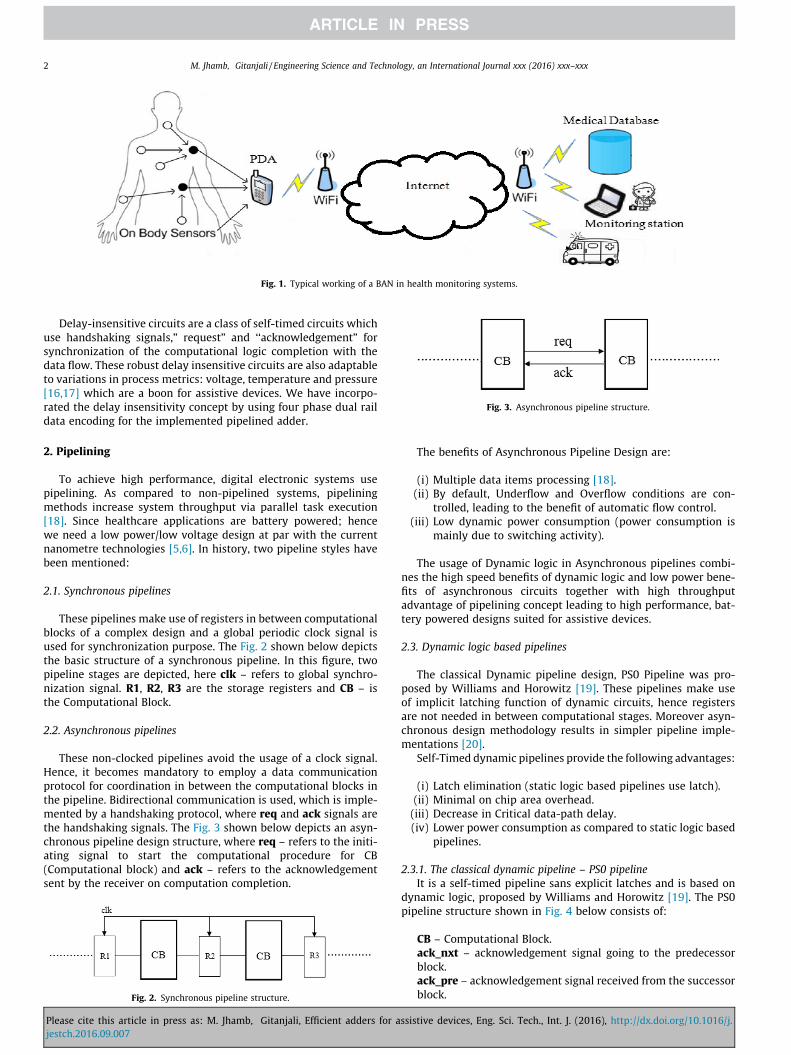
Fig. 1. Typical working of a BAN in health monitoring systems.
Fig. 3. Asynchronous pipeline structure.
2 M. Jhamb, Gitanjali / Engineering Science and Technology, an International Journal xxx (2016) xxx–xxx
Delay-insensitive circuits are a class of self-timed circuits whichuse handshaking signals,” request” and ‘‘acknowledgement” forsynchronization of the computational logic completion with thedata flow. These robust delay insensitive circuits are also adaptableto variations in process metrics: voltage, temperature and pressure[16,17] which are a boon for assistive devices. We have incorpo-rated the delay insensitivity concept by using four phase dual raildata encoding for the implemented pipelined adder.
2. Pipelining
To achieve high performance, digital electronic systems usepipelining. As compared to non-pipelined systems, pipeliningmethods increase system throughput via parallel task execution[18]. Since healthcare applications are battery powered; hencewe need a low power/low voltage design at par with the currentnanometre technologies [5,6]. In history, two pipeline styles havebeen mentioned:
2.1. Synchronous pipelines
These pipelines make use of registers in between computationalblocks of a complex design and a global periodic clock signal isused for synchronization purpose. The Fig. 2 shown below depictsthe basic structure of a synchronous pipeline. In this figure, twopipeline stages are depicted, here clk – refers to global synchro-nization signal. R1, R2, R3 are the storage registers and CB – isthe Computational Block.
2.2. Asynchronous pipelines
These non-clocked pipelines avoid the usage of a clock signal.Hence, it becomes mandatory to employ a data communicationprotocol for coordination in between the computational blocks inthe pipeline. Bidirectional communication is used, which is imple-mented by a handshaking protocol, where req and ack signals arethe handshaking signals. The Fig. 3 shown below depicts an asyn-chronous pipeline design structure, where req – refers to the initi-ating signal to start the computational procedure for CB(Computational block) and ack – refers to the acknowledgementsent by the receiver on computation completion.
Fig. 2. Synchronous pipeline structure.
Please cite this article in press as: M. Jhamb, Gitanjali, Efficient adders for ajestch.2016.09.007
The benefits of Asynchronous Pipeline Design are:
(i) Multiple data items processing [18].(ii) By default, Underflow and Overflow conditions are con-
trolled, leading to the benefit of automatic flow control.(iii) Low dynamic power consumption (power consumption is
mainly due to switching activity).
The usage of Dynamic logic in Asynchronous pipelines combi-nes the high speed benefits of dynamic logic and low power bene-fits of asynchronous circuits together with high throughputadvantage of pipelining concept leading to high performance, bat-tery powered designs suited for assistive devices.
2.3. Dynamic logic based pipelines
The classical Dynamic pipeline design, PS0 Pipeline was pro-posed by Williams and Horowitz [19]. These pipelines make useof implicit latching function of dynamic circuits, hence registersare not needed in between computational stages. Moreover asyn-chronous design methodology results in simpler pipeline imple-mentations [20].
Self-Timed dynamic pipelines provide the following advantages:
(i) Latch elimination (static logic based pipelines use latch).(ii) Minimal on chip area overhead.(iii) Decrease in Critical data-path delay.(iv) Lower power consumption as compared to static logic based
pipelines.
2.3.1. The classical dynamic pipeline – PS0 pipelineIt is a self-timed pipeline sans explicit latches and is based on
dynamic logic, proposed by Williams and Horowitz [19]. The PS0pipeline structure shown in Fig. 4 below consists of:
CB – Computational Block.ack_nxt – acknowledgement signal going to the predecessorblock.ack_pre – acknowledgement signal received from the successorblock.
ssistive devices, Eng. Sci. Tech., Int. J. (2016), http://dx.doi.org/10.1016/j.
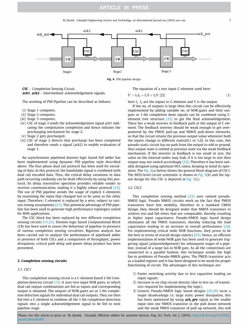
Fig. 4. PS0 pipeline design.
M. Jhamb, Gitanjali / Engineering Science and Technology, an International Journal xxx (2016) xxx–xxx 3
CSC – Completion Sensing Circuit.ack1, ack2 – Intermediate acknowledgement signals.
The working of PS0 Pipeline can be described as follows:
(i) Stage 1 computes.(ii) Stage 2 computes.(iii) Stage 3 computes.(iv) CSC of stage 3 sends the acknowledgement signal ack1 indi-
cating the computation completion and hence initiates theprecharging mechanism for stage 2.
(v) Stage 2 gets precharged.(vi) CSC of stage 2 detects that precharge has been completed
and therefore sends a signal (ack2) to enable evaluation ofstage 1.
An asynchronous pipelined domino logic based full adder hasbeen implemented using dynamic PS0 pipeline style describedabove. The four-phase dual rail protocol has been used for encod-ing of data. In this protocol, the handshake signal is combined withdual rail encoded data. Thus, the critical delay variations in datapath occurring randomly can be dealt effectively by using this pro-tocol. Its delay insensitive operation provides reliable sender toreceiver communication, making it a highly robust protocol [15].The use of PS0 pipeline avoids the usage of explicit C-elementsby examining the input that changed last to be same as the otherinput. Therefore; C-element is replaced by a wire, subject to vari-ous timing assumptions [21]. This potential advantage of PS0 pipe-line has been used to generate high performance topologies suitedfor BAN applications.
The CSC block has been replaced by two different completionsensing circuits [15,23]. Domino logic based Computational Block(CB) has been used to assess the behaviour of pipeline in presenceof various completion sensing circuitries. Rigorous analysis hasbeen carried out to analyze the performance of pipelined adderin presence of both CSCs and a comparison of throughput, powerdissipation, critical path delay and power delay product has beenpresented.
3. Completion sensing circuits
3.1. CSC1
This completion sensing circuit is a C-element based 2-bit Com-pletion detector circuit [15]. It uses two-input NOR gates, to whichdual rail output combinations are fed as inputs and correspondingoutput is obtained. The outputs of NOR-gates act as 1-bit comple-tion detection signals for individual dual rail outputs. They are thenfed into a C-element to combine all the 1-bit completion detectionsignals into a single acknowledgement signal to be fed to nextpipeline stage.
Please cite this article in press as: M. Jhamb, Gitanjali, Efficient adders for ajestch.2016.09.007
The equation of a two input C-element used here:
Y0 ¼ I1I2 þ I1Y þ I2Y ½22� ð1Þhere I1, I2 are the inputs to C-element and Y is the output.
If the no. of outputs is large then this circuit can be effectivelyimplemented by adding suitable no. of NOR-gates and their out-puts or 1-bit completion done signals can be combined using C-element tree structure [15] to get the final acknowledgement.There lies a weak inverter in feedback path at the output of C ele-ment. The feedback inverter should be weak enough to get over-powered by the PMOS pull-up and NMOS pull-down networks,so that the circuit retains the previous output value whenever boththe inputs change to different states{0,1 or 1,0}. In this case, thispseudo-static circuit has no path from the output to vdd or ground,thus output state is settled at previous state via the weak feedbackmechanism. If the inverter in feedback is too small in size, thevalue on the internal nodes may leak, if it is too large in size thenoutput may not switch accordingly [22]. Therefore it has been suit-ably designed using optimumW/L ratios, keeping in mind its oper-ation. The Fig. 5(a) below shows the general block diagram of CSC1.The MOS-level circuit schematic is shown in Fig. 5(b) and the lay-out design for this CSC is depicted in Fig. 5(c).
3.2. CSC2
This completion sensing method [23] uses ratioed pseudo-NMOS logic. Pseudo NMOS circuits work on the fact that PMOStransistors have low mobility, therefore in a standard CMOSdesign, they should be designed wider that NMOS transistors toachieve rise and fall times that are comparable, thereby resultingin higher input capacitance. Pseudo-NMOS logic based designeliminates all the PMOS transistors, thereby reducing the loadcapacitance leading to an increase in overall performance [24].For implementing critical wide NOR functions, they prove to bethe best in terms of overall design metrics [25]. Hence, an efficientimplementation of wide-NOR gate has been used to generate trig-gering signal (acknowledgement) for subsequent stages of a pipe-line, instead of a large fan-in NOR gate. As all the connections areconnected in a parallel fashion, this technique avoids the highfan-in problems of Pseudo-NMOS gates. The PMOS transistor actsas a loaded register and it has been designed to be weak for properfunctioning of circuit. The advantages of this technique are:
1) Faster switching activity due to less capacitive loading oninput signals.
2) Increase in on chip circuit density (due to less no. of transis-tors required for implementing the logic).
3) Generic Pseudo-NMOS logic based designs [25,26] incur amajor disadvantage i.e. large static power dissipation, thishas been optimized by using ack_pre signal as the enableinput into one NMOS transistor in the pull down networkand the weak PMOS transistor of pull-up network, this will
ssistive devices, Eng. Sci. Tech., Int. J. (2016), http://dx.doi.org/10.1016/j.
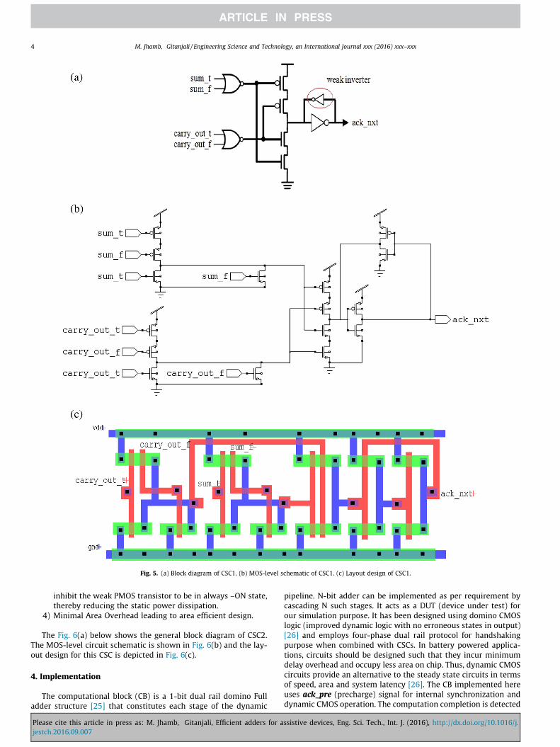
Fig. 5. (a) Block diagram of CSC1. (b) MOS-level schematic of CSC1. (c) Layout design of CSC1.
4 M. Jhamb, Gitanjali / Engineering Science and Technology, an International Journal xxx (2016) xxx–xxx
inhibit the weak PMOS transistor to be in always –ON state,thereby reducing the static power dissipation.
4) Minimal Area Overhead leading to area efficient design.
The Fig. 6(a) below shows the general block diagram of CSC2.The MOS-level circuit schematic is shown in Fig. 6(b) and the lay-out design for this CSC is depicted in Fig. 6(c).
4. Implementation
The computational block (CB) is a 1-bit dual rail domino Fulladder structure [25] that constitutes each stage of the dynamic
Please cite this article in press as: M. Jhamb, Gitanjali, Efficient adders for ajestch.2016.09.007
pipeline. N-bit adder can be implemented as per requirement bycascading N such stages. It acts as a DUT (device under test) forour simulation purpose. It has been designed using domino CMOSlogic (improved dynamic logic with no erroneous states in output)[26] and employs four-phase dual rail protocol for handshakingpurpose when combined with CSCs. In battery powered applica-tions, circuits should be designed such that they incur minimumdelay overhead and occupy less area on chip. Thus, dynamic CMOScircuits provide an alternative to the steady state circuits in termsof speed, area and system latency [26]. The CB implemented hereuses ack_pre (precharge) signal for internal synchronization anddynamic CMOS operation. The computation completion is detected
ssistive devices, Eng. Sci. Tech., Int. J. (2016), http://dx.doi.org/10.1016/j.

Fig. 6. (a) Block diagram of CSC2. (b) MOS level schematic of CSC2. (c) Layout design of CSC2.
M. Jhamb, Gitanjali / Engineering Science and Technology, an International Journal xxx (2016) xxx–xxx 5
using acknowledgement signal from event termination sensingtopologies that work in combination with the CB. Hence handshak-ing is performed effectively. The inputs to CB are dual rail datainputs a_t, b_t, cin_t, cin_f (carry inputs) which result in dual railoutputs sum_t, sum_f(sum), carry_out_t, carry_out_f (carryoutputs). The block diagram of a single pipeline stage is shown inFig. 7(a) and the MOS level implementation of CB is depicted inFig. 7(b).
The Table 1 presented below depicts the characteristics of theCB at 25 �C temperature, 1.2 V supply voltage, where
Tplh – refers to the delay incurred when the output signal risesto 50% of vdd(undergoes low to high transition).Tphl – refers to the delay incurred when the output signal falls to50% of vdd(undergoes high to low transition).Tpd – Average propagation delay.Pdiss – Power Dissipation.
5. Simulation and results
The SPICE-level simulations were carried out using HSpice (�Avant! Corporation) at 90 nm TSMC technology with supply volt-ages ranging from vdd = 0.8 V to 1.2 V and temperature was keptconstant at 25 �C. We have considered a 3 stage pipelined adder
Please cite this article in press as: M. Jhamb, Gitanjali, Efficient adders for ajestch.2016.09.007
for performance evaluation of the synchronous and asynchronousversions of the dual rail adder. The graph depicted below inFig. 8 presents a comparison of total power dissipation and criticalpath delay for asynchronous pipelined adder with its correspond-ing synchronous counterpart.
As observed from this graph, power dissipation has increasedand delay has decreased with increase in supply voltage. The asyn-chronous pipelined system performs better than the synchronoussystem as depicted by the decrease in power and delay values fromthe graph. Hence, it will provide high throughput as compared toits synchronous counterpart. Moreover, its energy efficient opera-tion (due to low power dissipation) depicts its ability to be incor-porated into assistive technology devices.
The asynchronous domino logic based pipelined adder has beenimplemented with two different completion detection approaches.We have considered a three stage pipelined system for perfor-mance analysis. It has been simulated with above mentioned pro-cess parameters and performance of both completion sensingapproaches has been compared by analyzing Power dissipation,Worst case delays, Latency and Throughput of the pipelined sys-tem. The Table 2 shown below depicts the variation of power dis-sipation and critical path delay for both the CSCs. Power Delayproduct is also calculated at all the values of vdd to ascertain theoverall performance of circuit designs.
ssistive devices, Eng. Sci. Tech., Int. J. (2016), http://dx.doi.org/10.1016/j.
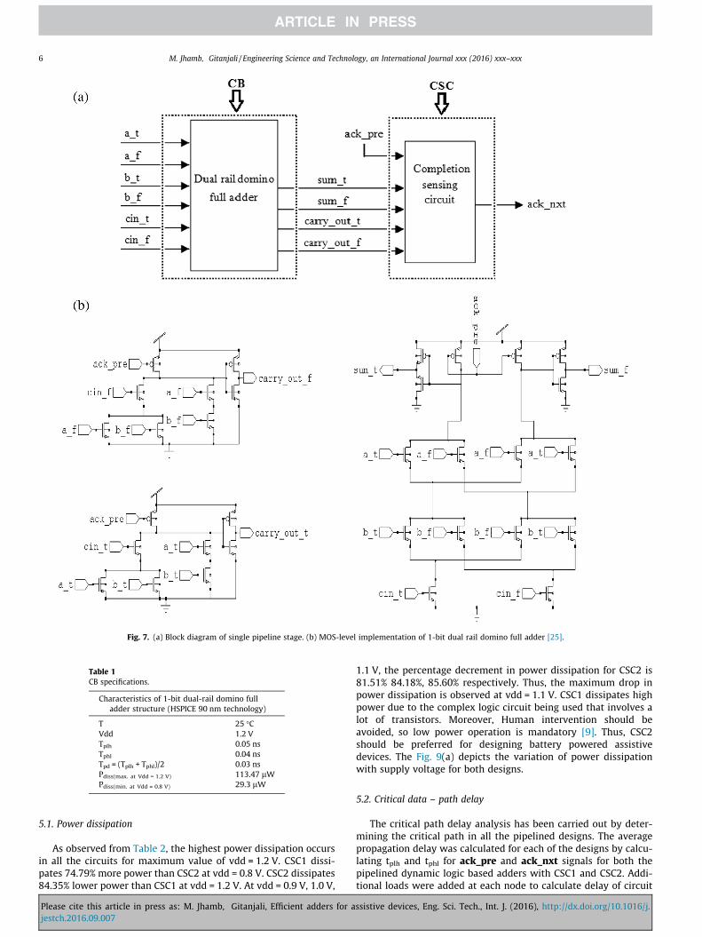
Fig. 7. (a) Block diagram of single pipeline stage. (b) MOS-level implementation of 1-bit dual rail domino full adder [25].
Table 1CB specifications.
Characteristics of 1-bit dual-rail domino fulladder structure (HSPICE 90 nm technology)
T 25 �CVdd 1.2 VTplh 0.05 nsTphl 0.04 nsTpd = (Tplh + Tphl)/2 0.03 nsPdiss(max. at Vdd = 1.2 V) 113.47 lWPdiss(min. at Vdd = 0.8 V) 29.3 lW
6 M. Jhamb, Gitanjali / Engineering Science and Technology, an International Journal xxx (2016) xxx–xxx
5.1. Power dissipation
As observed from Table 2, the highest power dissipation occursin all the circuits for maximum value of vdd = 1.2 V. CSC1 dissi-pates 74.79% more power than CSC2 at vdd = 0.8 V. CSC2 dissipates84.35% lower power than CSC1 at vdd = 1.2 V. At vdd = 0.9 V, 1.0 V,
Please cite this article in press as: M. Jhamb, Gitanjali, Efficient adders for ajestch.2016.09.007
1.1 V, the percentage decrement in power dissipation for CSC2 is81.51% 84.18%, 85.60% respectively. Thus, the maximum drop inpower dissipation is observed at vdd = 1.1 V. CSC1 dissipates highpower due to the complex logic circuit being used that involves alot of transistors. Moreover, Human intervention should beavoided, so low power operation is mandatory [9]. Thus, CSC2should be preferred for designing battery powered assistivedevices. The Fig. 9(a) depicts the variation of power dissipationwith supply voltage for both designs.
5.2. Critical data – path delay
The critical path delay analysis has been carried out by deter-mining the critical path in all the pipelined designs. The averagepropagation delay was calculated for each of the designs by calcu-lating tplh and tphl for ack_pre and ack_nxt signals for both thepipelined dynamic logic based adders with CSC1 and CSC2. Addi-tional loads were added at each node to calculate delay of circuit
ssistive devices, Eng. Sci. Tech., Int. J. (2016), http://dx.doi.org/10.1016/j.

Fig. 8. Power-delay comparison of synchronous and asynchronous pipelined system.
Table 2Variation of power and delay for CSCs in 90 nm technology.
VDD (volts) CSC Delay (ns) Power (lW) Power delay product (fJ)
0.8 CSC1 0.78 26.54 20.77CSC2 0.19 6.69 1.27
0.9 CSC1 0.77 48.42 37.28CSC2 0.18 8.95 1.61
1 CSC1 0.54 73.21 39.53CSC2 0.17 11.58 1.96
1.1 CSC1 0.50 100.09 50.04CSC2 0.16 14.41 2.30
1.2 CSC1 0.39 110.62 43.14CSC2 0.09 17.31 1.55
M. Jhamb, Gitanjali / Engineering Science and Technology, an International Journal xxx (2016) xxx–xxx 7
components. As observed from Table 2, a significant drop in delaywas observed at vdd = 1.2 V for CSC2 which was 76.92% lower thanCSC1 at the same voltage. At vdd = 0.9 V, 1.0 V, 1.1 V the improve-ments in speed are 76.62%, 68.51%, 68% respectively. The worstcase delay of CSC1 (at vdd = 0.8 V) was 75.2% greater than that ofCSC2 at the same supply voltage. Thus CSC2 should be preferredfor high speed operation. The Fig. 9(a) depicts the variation of crit-ical path delay with supply voltages for both designs.
5.3. Power-delay product
The prime design goal of high performance systems is toachieve a low power delay product. To analyze the energy dissipa-tion over a switching event, power-delay product has been calcu-lated for all voltages spanning from vdd = 0.8 V to 1.2 V. Thisproduct depicts a tradeoff between delay incurred and power dis-sipated in a design. Dynamic circuits provide the benefit of highspeed operation with the drawback of higher power dissipation.But the use of asynchronous design methodology has proved ben-eficial in lowering the power delay product. As observed fromTable 2, the asynchronous fine grain dynamic pipelined adderstructure dissipates highest energy (per switching event) atvdd = 1.1 V when CSC1 was used for completion detection which
Please cite this article in press as: M. Jhamb, Gitanjali, Efficient adders for ajestch.2016.09.007
is 95.39% higher than CSC2. At vdd = 0.9 V, 1 V, 1.2 V, the decre-ment in PDP for CSC2 with respect to CSC1 is 95.67%, 95.02%,96.38% respectively. Thus, the maximum drop in PDP for CSC2 overCSC1 occurs at vdd = 1.2 V which is 96.38%. The PDP of CSC2 was93.85% lower at lowest considered voltage (vdd = 0.8 V) as com-pared to CSC1, depicting its potential advantage in BANs applica-tions. The Fig. 9(b) depicts the variation of power delay productfor all values of supply voltage for both CSCs.
5.4. Throughput and latency
Throughput and per-stage latency are critical design parame-ters of prime concern for designers because they depict whethera circuit is suited for certain applications or not. For evaluatingthe throughput and latency we have taken different values ofvdd spanning from 0.8 V to 1.2 V at T = 25 �C. The variation ofthroughput with variation in supply voltage and the variation ofper stage forward latency with increasing supply voltages has beendepicted graphically. By replacing CSC block with above imple-mented completion sensing circuits, throughput has been com-pared for both the designs to ascertain their performance. ThePS0 pipeline structure has been considered for implementing theadder designs with both completion sensing approaches. Theparameter required to determine the throughput is the cycle timewhich is the time required for one computation cycle of a pipeline.
The cycle time for a PS0 PIPELINE ¼ 3TCB þ Tpre þ 2TCSC ½18;19�ð2Þ
The forward latency per stage is given by: L = Forward Latencyper stage = TCB [18,19] which is same for both the addersimplemented.
From Eq. (2), TCSC = Time required for completion detection bythe CSC, Tpre = Precharge Time.
The Fig. 10(a) depicts the latency variation with supply voltageand Fig. 10(b) depicts throughput variation with supply voltage forboth schemes.
Observed values of latency from the Fig. 10(a) and throughputfrom Fig. 10(b) lead to the following facts:
ssistive devices, Eng. Sci. Tech., Int. J. (2016), http://dx.doi.org/10.1016/j.

Fig. 9. (a) Power dissipation and critical path delay variation. (b) Power-delay product comparison.
8 M. Jhamb, Gitanjali / Engineering Science and Technology, an International Journal xxx (2016) xxx–xxx
� Forward Latency is dependent on supply voltage. It decreaseswith increase in supply voltage.
� Lowest per stage forward latency is observed at vdd = 1.2 Vwhich is 0.03 ns.
� CSC2 gave the best throughput results, depicting high perfor-mance of this completion sensing circuit in dynamic pipelinedesign. Max. Throughput achievable using CSC2 was 3.31 Gspswhich was observed to be 198.67% higher than that usingCSC1 at vdd = 1.2 V, but at the cost of high power dissipation.
� CSC2 gave 178.59%, 134.39%, 142.5% improvements in through-put at supply voltages, vdd = 0.9 V, 1.0 V, 1.1 V respectively.Even at a low voltage of 0.8 V, pipelined adder with CSC2 gavea throughput of 1.37 Gsps which was 162% higher than thethroughput obtained by considering CSC1 as completion detec-tion approach. Therefore a significant improvement in through-put is achievable even at low voltages, making this designsuitable for assistive devices.
5.5. Circuit complexity
In current deep-sub micron CMOS technologies, where multipletransistors are integrated on a single chip, circuit complexity is amajor design metric. It is measured in terms of total number oftransistors required to implement a logic function. In the pipelinedcircuit designed above, number of transistors per stage of the
Please cite this article in press as: M. Jhamb, Gitanjali, Efficient adders for ajestch.2016.09.007
dynamic pipeline have been calculated which are much lesser innumber owing to the fact that dynamic CMOS logic has been usedfor implementation of the computational block. As depicted fromthe graph, the circuit complexity (in terms of number of transis-tors) is highest for CSC1.
In terms of transistor count, CSC2 outshines CSC1 depicting theinherent advantage of Pseudo NMOS based design of reducing thetransistor count. The Fig. 11(a) depicts the transistor count for bothschemes.
5.6. Layout area
The VLSI circuit design layout has been designed in accor-dance with standard design rules. Two metal wire based layouthas been designed for each of the completion sensing circuitsand DRC (Design Rule Check) and LVS (Layout vs. Schematiccheck) was performed to ascertain the equality of circuits at lay-out design level and the schematic level. The Table 3 depictedbelow shows the layout area occupied for a standard CSC celldesign.
The area requirement is higher for CSC1 due to the complex cir-cuitry used resulting in large area overhead. Hence area wise,Pseudo NMOS based CSC2 outperforms the C-element basedCSC1. Fig. 11(b) depicts the layout area comparison for CSC1 andCSC2.
ssistive devices, Eng. Sci. Tech., Int. J. (2016), http://dx.doi.org/10.1016/j.

Fig. 11. (a) No. of transistors per stage. (b) Layout area comparison.
Fig. 10. (a) Latency vs. vdd. (b) Throughput vs. vdd.
Table 3Layout area occupied by different completion sensingcircuits.
Implementation style Layout area (Mk2)
CSC1 0.0115 Mk2
CSC2 0.0095 Mk2
M. Jhamb, Gitanjali / Engineering Science and Technology, an International Journal xxx (2016) xxx–xxx 9
Please cite this article in press as: M. Jhamb, Gitanjali, Efficient adders for ajestch.2016.09.007
6. Conclusion
The BANs operate with stringent timing requirements. Hence,real-time operation of BANs requires low latency components.The simulation results depict that the asynchronous pipelinedadder design with CSC2 (Pseudo NMOS based completion sensingapproach) achieves a 75.64% improvement in operating speedand 162% improvement in throughput at a low voltage of 0.8 V.Moreover, energy efficiency, which is depicted by power delay pro-duct has improved by 93.85% at this voltage level. Thus, CSC2 isable to achieve high performance with low power consumptionand lower silicon area requirement as compared to CSC1, therebydepicting its ability to be incorporated into battery powered assis-tive devices for BAN health care systems.
References
[1] Qammer H. Abbasi, Masood Ur-Rehman, Khalid Qaraqe, Akram Alomainy(Eds.), Advances in Body-Centric Wireless Communication: Applications andstate-of-the-art, IET Digital Library, 2016, http://dx.doi.org/10.1049/PBTE065E.Telecommunications.
[2] Câmara Daniel, Nikaein Navid, Wireless Public Safety Networks 2: ASystematic Approach Computers, Elsevier, June 2016, ISBN 9780081010693.
[3] Masuch Jens, Manuel Delgado-Restituto, Ultra low power transceiver forwireless body area networks, in: Analog Circuits and Signal Processing,Springer, 2013, ISBN 978-3-319-00098-5.
[4] Guang-Zhong Yang (Ed.), Body Sensor Networks, Computer Science, HCI,Springer, 2014 (ISBN: 978-1-4471-6347-9).
[5] Akram Alomainy, Raffaele Di Bari, Qammer H. Abbasi, Yifan Chen, Co-Operative and Energy Efficient Body Area and Wireless Sensor Networks forHealthcare Applications, Academic Press, 2014. ISBN: 978-0-12-800736-5(Sciencedirect).
[6] K. Thotahewa, J.M. Redoute, M.R. Yuce, Ultra Wideband Body Area Networks,in: Engg. Circuits and Systems, Springer, 2014, ISBN 978-3-319-05287-8.
[7] Aleksander Milenkovic, Chris Otto, Emil Jovanov, Wireless networks forpersonal health monitoring: issues and implementation, Comput. Commun.(2006) (Sciencedirect).
[8] Hernandez Marco, Mucchi Lorenzo, Body Area Networks Using IEEE 802.15.6,Implementing the Ultra Wideband Physical Layer, 978-0-12-396520-2.,Academic Press, 2014 (Sciencedirect).
[9] Kumar Pankaj, Rajender Kumar Sharma, Low voltage high performance hybridfull adder, Eng. Sci. Technol. Int. J. 19 (1) (March 2016) 559–565, http://dx.doi.org/10.1016/j.jestch.2015.10.001. ISSN: 2215-0986 (Sciencedirect).
[10] Shoba Mohan, Nakkeeran Rangaswamy, GDI based full adders for energyefficient arithmetic applications, Eng. Sci. Technol. Int. J. 19 (1) (March 2016)485–496, http://dx.doi.org/10.1016/j.jestch.2015.09.006. ISSN: 2215-0986(Sciencedirect).
[11] Jhamb Mansi, Garima, Lohani Himanshu, Design, implementation andperformance comparison of multiplier topologies in power-delay space, Eng.Sci. Technol. Int. J. 19 (1) (March 2016) 355–363, http://dx.doi.org/10.1016/j.jestch.2015.08.006. ISSN: 2215-0986 (Sciencedirect).
[12] Eng Sue Chew, Myint Wai Phyu, Wang Ling Goh, Ultra low-power full-adderfor biomedical applications, in: IEEE International Conference of ElectronDevices and Solid-State Circuits, 2009. pp 115–1182, 5–27 Dec. 2009.
[13] Janusz A. Brzozowski, Johan H. Seger, Asynchronous Circuits, Springer, 1995,ISBN 978-1-4612-8698-1.
[14] Birtwistle Graham, Davis Alan, Asynchronous Digital Circuit Design, Springer,1995. ISBN: 978-3-540-19901-4.
[15] Zhengfan Xia, Masanori Hariyama, Michitaka Kameyama, Asynchronousdomino logic based pipeline design based on constructed critical data path,IEEE Trans. VLSI Syst. 23 (4) (2015).
[16] I. Lemberski, Peter Fiser, Dual-rail asynchronous logic multi-levelimplementation, Integrat. VLSI J. 47 (1) (January 2014) 148–158.
[17] A.J. Martin et al., The first asynchronous microprocessor; the test results, ACMSIGARCH Comp. Arch. News 17 (4) (June 1989) 95–98.
[18] S.M. Nowick, High performance asynchronous pipelines design and test ofcomputers, IEEE 28 (5) (2011) 8–22.
[19] T.E. Williams, Self-timed rings and their application to division (Ph.D. thesis),Computer Systems Lab, Stanford University, 1991.
[20] I. Sutherland, Micropipelines, Comm. ACM 32 (1989) 720–723.
ssistive devices, Eng. Sci. Tech., Int. J. (2016), http://dx.doi.org/10.1016/j.

10 M. Jhamb, Gitanjali / Engineering Science and Technology, an International Journal xxx (2016) xxx–xxx
[21] Williams, Latency and throughput tradeoffs in self timed speed independentpipelines and rings, Tech. Rep. (1990). CSL-TR-90-431.
[22] Peter A. Beerel, Recep O. Ozdag, Marcos Feretti, A Designer’s Guide toAsynchronous VLSI, Cambridge University Press, 2010 (ISBN: 978-0521-87244-7).
[23] Mohammed Zia ur Rahman, Lindsay Kleeman, Mohammad Ashfak Habib,Recursive approach to the design of parallel self-timed adder, IEEE Trans. VLSISyst. (2014).
Please cite this article in press as: M. Jhamb, Gitanjali, Efficient adders for ajestch.2016.09.007
[24] I. Sutherland, Bob Sproull, David Harris, Logical Effort: Designing Fast CMOSCircuits, Morgan Kaufmann Publishers, 1999, ISBN 1-55860-557-6.
[25] Neil Weste, D. Harris, CMOS VLSI DESIGN: A Circuits and Systems Perspective,Addison Wesley, 2004.
[26] Sung Mo Kang, Yusuf Leblebici, CMOS Digital Integrated Circuits, Tata McGraw-HILL, 2003, ISBN 978-0-07-053077-5.
ssistive devices, Eng. Sci. Tech., Int. J. (2016), http://dx.doi.org/10.1016/j.