Design of High Efficiency Step-Down Switched Capacitor by Mengzhe

EFFICIENCY ENHANCEMENT TECHNIQUES
FOR SWITCHED MODE POWER ELECTRONICS
by
April (Yang) Zhao
A thesis submitted in conformity with the requirements
for the degree of Master of Applied Science
The Edward S. Rogers Sr. Department of Electrical and Computer Engineering
University of Toronto
© 2011 Copyright by April (Yang) Zhao
ii
Abstract
Efficiency Enhancement Techniques for Switched Mode Power Electronics
April (Yang) Zhao
Master of Applied Science
The Edward S. Rogers Sr. Department of Electrical and Computer Engineering
University of Toronto
© 2011
In the design of the state-of-the-art electronic products, power management circuits play a
very important role for the enhancement of overall system efficiency. Switched mode DC-
DC converter is an increasingly popular power management circuit due to its superior
power conversion efficiency. This thesis introduces two efficiency optimization techniques
for switched mode power electronic circuits. First, a novel one-step dead-time optimization
digital control technique is discussed. This dead-time optimization algorithm can
automatically adjust the dead-time on-the-fly according to the circuit operating conditions.
An overall 2 to 4% improvement in efficiency can be realized. Second, an energy
conservation based high-efficiency dimmable multi-channel LED driver is discussed. An
auxiliary power switched is use to allow free wheeling of the inductor current during the
load disconnect period. The sequential burst mode PWM current sharing scheme with
dimming capability can effectively reduce design complexity and cost. The proposed LED
driver provides a practical solution for the realization of LED back lighting units in the flat
panel TVs with local dimming capability according to the video content.

iii
Acknowledgements
My research at the University of Toronto started in the summer of 2008, when I first
conducted a research project with Prof. Wai Tung Ng. Thereafter, he gave me many
opportunities to attend various IEEE international conferences, which have broaden my
horizon and inspired my interest for research work. I, above all, would like to express my
deepest gratitude to my supervisor, Prof. Ng, for his great sense of responsibility and
continuous support in my research ever since. His broad knowledge, his logical thinking
and dedication have been of great value for me. This thesis would not have been possible
without his constant encouraging and guidance.
In addition, from our research group, I would like to thank Jing Wang and Armin
Akhavan Fomani for their help in the past few years. I also want to thank all the people in
our lab, including Sherrie Xie, Gang Xie, Amy Shen, Andrew Shorten, Pearl Cao, Juming
Lee, Taylor Yu and Easton Tu. They have all inspired me through our interactions and
during the times we spent together at work.
Special thanks to Prof. Hyoung Gin Nam from Sun Moon University, Korea for
introducing me to LED backing lighting technology.
Financial supports from Auto21, Canada’s Network Centers of Excellence and
Chungnam Display R&D Cluster Center (CDRC), Korea are gratefully appreciated.
My appreciation should also extend to my friends in our Bible Study group and church,
Max Ridout, Andresa Marinho, Jamie Nay, Dave Leynch. Their kindly words and prayer
have helped me to calm my mind and offered me with infinite courage and hope. Also, My
parents in China, they have been very supportive and understanding on all the decisions I
have made. I would like to thank them for their unconditional love and patience.
Last but not least, I will also thank my daughter, Nicole, for “training” me to be an
accountable and loving person. The time management skills she “forced” me to learn have
made me capable of handling my research work and being a mother at the same time.

iv
The seven years I spent in U of T is the most valuable periods of my life, which I
certainly shall cherish forever. After surviving through many difficulties and frustration,
the learning process and research work have become more enjoyable than ever in my
memory.

v
EFFICIENCY ENHANCEMENT TECHNIQUES
FOR SWITCHED MODE POWER ELECTRONICS
CHAPTER 1: A Brief Introduction on Switched Mode DC-DC
Converters
1.1 BASICS OF DC-DC SWITCHED MODE CONVERTERS ............................................................................. 2
1.2 CHALLENGE OF POWER MANAGEMENT CIRCUIT AND A BRIEF TECHNOLOGY REVIEW ....................... 4
1.3 THESIS ORGANIZATION ...................................................................................................................... 6
CHAPTER 2: One-step Digital Dead-time Correction for DC-DC
Converter
2.1 SIGNIFICANCE OF DEAD-TIME CORRECTION ....................................................................................... 8
2.2 EFFICIENCY IMPROVEMENT WITH OPTIMUM DEAD-TIME ................................................................ 11
2.3 LITERATURE REVIEW ........................................................................................................................ 13
2.3.1 ADAPTIVE DELAY TECHNIQUE ................................................................................................................. 13
2.3.2 PREDICTIVE GATE DRIVE SCHEME [4]-[6] ................................................................................................. 14
2.3.3 DEAD-TIME SEARCH ALGORITHM............................................................................................................. 15
2.4 OPTIMUM DEAD-TIME FUNCTIONAL MECHANISM .......................................................................... 15
2.5 OVERALL OPERATION ....................................................................................................................... 19
2.6 SYSTEM FUNCTION MODULE DESCRIPTION ...................................................................................... 20
2.6.1 ONE-STEP DEAD-TIME CORRECTION ALGORITHM ....................................................................................... 21
2.6.2 BODY-DIODE CONDUCTION DETECTION CIRCUIT ......................................................................................... 23
2.6.3 BODY-DIODE CONDUCTION PULSE WIDTH MEASUREMENT .......................................................................... 25
2.6.4 HYBRID DPWM WITH PROGRAMMABLE DEAD-TIME GENERATION ................................................................ 27

vi
2.6.5 OUTPUT STAGE DESIGN SPECIFICATIONS ................................................................................................... 32
2.7 EXPERIMENTAL RESULTS .................................................................................................................. 34
2.7.1 CONVERSION EFFICIENCY DURING STEADY-STATE ........................................................................................ 34
2.7.2 CONVERSION EFFICIENCY DURING LOAD TRANSIENT .................................................................................... 37
2.8 CONCLUSION .................................................................................................................................... 41
CHAPTER 3: An Energy Conservation Based High-efficiency Dimmable
Multi-channel LED Driver
3.1 BACK-LIGHTING UNITS WITH LOCAL DIMMING FOR FLAT PANEL DISPLAYS ...................................... 44
3.2 LITERATURE REVIEW ........................................................................................................................ 45
3.2.1 SELF-ADAPTIVE DRIVES .......................................................................................................................... 46
3.2.2 ONE-COMPARATOR COUNTER BASED INDUCTOR CURRENT SAMPLING METHOD .............................................. 47
3.2.3 HIGH FREQUENCY PWM DIMMING ........................................................................................................ 49
3.3 SYSTEM OPERATION ........................................................................................................................ 50
3.4 DC-DC BOOST CONVERTER MULTI-CHANNEL LED DRIVER DESIGN.................................................... 54
3.4.1 TRANSISTOR SWITCHES (SMAIN AND SAUX) ................................................................................................. 54
3.4.3 LED CURRENT DIMMING SWITCH............................................................................................................ 56
3.4.4 ANALOG-TO-DIGITAL CONVERTER (ADC) ................................................................................................. 56
3.5 SYSTEM FUNCTIONAL MODULE DESCRIPTION .................................................................................. 57
3.5.1 BURST MODE PWM DIMMING .............................................................................................................. 57
3.5.2 MULTI-LOAD BURST MODE PWM SEQUENTIAL DIMMING SCHEMES ............................................................. 59
3.5.3 CLOSE LOOP CURRENT MODE PI CONTROLLER ............................................................................................ 60
3.5.4 ENERGY CONSERVATION BASED CLOSE LOOP PI CONTROL SCHEME ............................................................... 63
3.5.5 LED SELECTION ................................................................................................................................... 65
3.5.6 DESIGN SPECIFICATIONS ........................................................................................................................ 66

vii
3.6 SYSTEM VERIFICATION AND EXPERIMENTAL RESULTS ..................................................................... 70
3.6.1 MULTI-CHANNEL LOAD SWITCHING TRANSIENT TEST .................................................................................. 71
3.6.2 MULTI-CHANNEL LED DRIVER EFFICIENCY TEST ......................................................................................... 72
3.7 CONCLUSION .................................................................................................................................... 73
CHAPTER 4: Conclusions

viii
List of Tables
Table 2.1: Summary of design parameters for a 6 V to 1 V DC-DC buck converter .......... 34
Table 3.1: Power switches loss evaluation for efficiency optimization ............................ 55
Table 3.2: Dimming switch loss evaluation for efficiency optimization .......................... 56
Table 3.3 The influence of supply line variation on control loop ..................................... 62
Table 3.4 Summary of design parameters for a 4.5 V to 14 V DC-DC boost converter .. 69
Table 3.5: Testing Conditions of the 4.5 V to 14 V 180 mA 3-channel LED driver........ 70

ix
List of Figures
Figure 1.1: A typical topology of a DC-DC buck converter. .............................................. 2
Figure 1.2: MOSFET gate driver signals with different driving strength ........................... 4
Figure 2.1: Timing diagram showing the relationship between the MOSFETs DPWM
signals and the actual gate driving signals ................................................... 10
Figure 2.2: Cross-conduction power loss approximation for different supply voltages and
operating frequencies. .................................................................................. 10
Figure 2.3: Percentage power savings for different output voltages and operating
frequencies. .................................................................................................. 11
Figure 2.4: Experimental setup for optimum dead-time identification. ......................... 12
Figure 2.5: Power conversion comparison for different dead-times. ............................. 12
Figure 2.6: Adaptive delay circuit and its timing diagram for dead-time generation. ... 14
Figure 2.7: MOSFET switching diagrams for optimum, long and short dead-time cases.17
Figure 2.8: Current flow through LS MOSFET body-diode when dead-time is too long.18
Figure 2.9: Current flow through Vdd to ground when dead-time is too short .............. 18
Figure 2.10: System level diagram of the implement of one-shot dead-time correction
algorithm. ..................................................................................................... 20
Figure 2.11: A flow chart representation of the one-step dead-time optimization algorithm.
22
Figure 2.12: Switching diagrams for NOR gate body-diode conduction detection circuit. .
..................................................................................................................... 24
x
Figure 2.13: Body-diode conduction pulse width measurement using a delay line and delay
lock loop....................................................................................................... 26
Figure 2.14: Timing diagram shows the formation of delay pulse. .................................. 26
Figure 2.15: Timing diagram for the body-diode conduction pulse width measurement
decoder. ........................................................................................................ 27
Figure 2.16: The construction of 1.25ns delay cell with 2 delay paths. ........................... 29
Figure 2.17: Schematic of the delay element. .................................................................. 29
Figure 2.18: Hybrid DPWM signal generation with programmable dead-time incorporated.
31
Figure 2.19: Timing diagram of HS and LS DPWM signal generation with programmable
dead-time...................................................................................................... 32
Figure 2.20: Output stage PCB layout. ............................................................................. 33
Figure 2.21: The NOR gate body-diode conduction detection waveform (steady-state)
shows a non-optimum dead-time condition. ................................................ 35
Figure 2.22: Body-diode conduction detection waveform (steady-state) shows body-diode
condition is eliminated with dead-time correction algorithm. ..................... 36
Figure 2.23: Power conversion efficiency is increased by 2% to 4% compared with non-
optimum dead-times case. ............................................................................ 36
Figure 2.24: Switching waveforms show that body-diode conduction gradually increases
when current experiences a sudden increase from 0.1A to 4A eliminated with
dead-time correction algorithm. ................................................................... 38
Figure 2.25: A close-up view of the body-diode conduction at the 14th switching cycle
after the load current starts to change .......................................................... 39

xi
Figure 2.26: The inductor current waveform increases gradually during a load change from
0.1 A to 4 A. ................................................................................................. 40
Figure 2.27: Switching waveforms show that body-diode conduction is eliminated with
dead-time correction algorithm. ................................................................... 41
Figure 3.1: The luminance of LED can be dynamically adjusted according to image
content. ......................................................................................................... 45
Figure 3.2: LED driver with adaptive drive voltage for linear current regulator. .......... 46
Figure 3.3: A representation of the one-comparator counter based inductor current
sampling method. ......................................................................................... 48
Figure 3.4: High frequency series PWM dimming ........................................................ 50
Figure 3.5: A block diagram of the proposed LED back-lighting system consisting of a
flat panel active TFT matrix LCD screen, the LED BLU, the LED drivers
panel, LCD display control and BLU control unit.. ..................................... 51
Figure 3.6: LED driver unit contains 4 identical 3-channel LED driver design. ........... 52
Figure 3.7: An implementation of the 4 3 LED driver circuit. .................................... 53
Figure 3.8: LED driver dimming scheme ....................................................................... 58
Figure 3.9: Timing diagram for burst mode PWM multiplexing scheme with 100%
dimming ratio. .............................................................................................. 59
Figure 3.10: Timing diagram for burst mode PWM multiplexing scheme with arbitrary
dimming ratio. .............................................................................................. 60
Figure 3.11: Bode plot of control-to-output transfer function at Vg = 2.7 V for K = 10. 63
Figure 3.12: Timing diagram for arbitrary dimming duty ratios. ..................................... 65

xii
Figure 3.13: The relationship between full current, pulsating current and maximum rated
current in a LED........................................................................................... 66
Figure 3.14: The 4-layer PCB layout of the proposed 4 × 3 LED driver. ........................ 67
Figure 3.15: The 17 inch LED back-lighting unit with 34 LED regions. ....................... 68
Figure 3.16: Load current waveform during PWM dimming period, energy conservation
and pre-regulation period. ............................................................................ 71
Figure 3.17: Measured LED driver efficiency measurements for pre-regulation times equal
to1/16, 1/8 of PWM dimming period. .......................................................... 72

xiii
List of Abbreviations
HS High-side (MOSFET / Gate Driver)
LS Low-side (MOSFET / Gate Driver)
CCM Continues Conduction Mode
BLU Back-lighting Unit
CCFL Cold Cathode Fluorescent Light
Trise Rising Edge Delay, MOSFET Turn-on Time
Tfall falling Edge Delay, MOSFET Turn-off Time
DTrise Rising Edge Dead-time
DTfall Falling edge Dead-time
Vgate-low LS power MOSFET Gate-source Voltage
Vsw-node LS power MOSFET Drain-source Voltage
TFT Thin Film Transistor
Pswi_loss MOSFET Switching Power Loss
Pcon_loss MOSFET Conduction Power Loss
Rsen Sense Resistor Resistance
Vsen Output Sense Voltage

1
CHAPTER 1
A Brief Introduction on Switched Mode DC-DC Converters
Power management circuits are a family of circuits that can deliver the desired
voltages and power to the load in an energy efficient manner. [1] They can be found in all
kinds of electrical applications, such as microprocessors, infotainment devices, and
lighting equipment. There are two basic types of power management circuit: linear
regulator and switched mode regulator. Linear regulators offer a simpler and low cost
solution due to fewer component counts, while switched mode regulators offer a more
complex but energy efficient solution. Since reducing power consumption has become
increasingly important in electronic system design, switched mode regulators are
gradually becoming the mainstream power management solutions.
This chapter provides an overview of the operating principle of the switched mode
DC-DC converters and the challenge of designing power management circuits.

2
1.1 Basics of DC-DC Switched Mode Converters
In a DC-DC switched mode power supply, the DC input voltage is converted to a DC
output voltage with a larger or smaller magnitude, and possibly with opposite polarity or
isolation from the input. Figure 1.1 shows a typical topology of a DC-DC buck converter.
(Both NMOS and PMOS can be used as high side MOSFET, NMOS is used in this thesis
for switching analysis.) There are two operating phases in the more common continues
conduction mode (CCM). Phase 1 is the case when the high side (HS) MOSFET turns on
and the low side (LS) MOSFET turns off. Since input voltage is higher than output
voltage, inductor current flows from input to output with increasing magnitude. Phase 2
is the case when the HS MOSFET turns off and the LS MOSFET turns on. The inductor
current keeps flowing in the same direction with decreasing magnitude. Output voltage is
regulated through the continuous charging and discharging of the output capacitor. The
HS and LS gate drivers are placed in front of the HS and the LS MOSFETs to provide
Figure 1.1: A typical topology of a DC-DC buck converter.
LS
MOSFET
L
C Load
Switching
node
HS
MOSFET
LS
Gate Driver
Vin
HS
Gate Driver
BODY
DIODE
BODY
DIODE

3
sufficient driving strength to ensure fast turn-on and turn-off of the power MOSFETs.
The fundamental operating principle of the DC-DC converter with CMOS power
transistors requires complementary driving signals. Figure 1.2 shows the HS and the LS
gate driving signals in the cases of fast and slow switching transitions. Figure 1.2(a)
shows the ideal case where very fast gate driving signals are applied. The HS and the LS
MOSFET switching transitions happen simultaneously. Since there is always one
MOSFET turns on at any given time, the cross conduction from the supply line (Vdd) to
ground through the power switches can be eliminated. Figure 1.2(b) shows the case with
low gate driving strength. Due to the rising edge and falling edge delays (Trise, Tfall), i.e.
MOSFET turn-on and turn-off time, the actual DPWM pulse width is modified. There
could also exists a moment when both MOSFETs are conducting, resulting in a
potentially large shoot through current flowing from supply line to ground. In practical
cases, the zero MOSFET turn-on and turn-off time can never be achieved due to their
large gate capacitance and parasitic resistance in the gate drive circuit. In order to
eliminate cross conduction, the dead-times have to be introduced to the gate drive signals.
The length of the dead-time affects the conversion efficiency in a significant way. The
dead-time optimization issue will be addressed in Chapter 2.

4
1.2 Challenge of Power Management Circuit and a Brief Technology Review
Power management circuit plays a very important role in electronic system designs.
It can significantly affect the overall system efficiency. Optimizing system power
consumption continuously yields multiple benefits. In battery-operated device, the lower
the average power consumption, the longer the battery life or the smaller, lighter and
cheaper the battery can be. Even with the availability of unlimited power, such as in data
Figure 1.2: MOSFET gate driver signals with different driving strength.
(a) High gate driving strength
(b) Low gate driving strength
Trise
Duty cycle
HS Gate Driving Signal
LS Gate Driving Signal
Signal
HS Gate Driving Signal
LS Gate Driving Signal
Actual Duty cycle
Tfall
Take rising edge for example
(a)
(b)

5
centers, efficient power delivery and consumption can lead to a reduction in the cost for
the installation of heat sinks and other cooling mechanisms.
The main challenges of power management circuit are in the optimization of digital
power supply design and the system level design. The first challenge includes device
level and package level optimization. In the device level, the power switches are treated
as source of loss, which includes sub-threshold leakage and the dynamic power
dissipation. Traditionally, integrated power MOSFETs are realized using HV CMOS
technology. For converters operating from 1 MHz to 10 MHz, power MOSFET
technologies must be improved substantially to reduce frequency dependent loss
(dynamic loss). Solutions include HV CMOS, vertical power MOSFET using planar or
trench gate structures and lateral sub-micron DMOS, etc. Packaging is also a key aspect
in efficiency optimization. Parasitic resistive conduction loss can be very severe with the
increase of output current. Stray inductive losses also increase significantly with higher
switching frequencies. The communication between the load and the digitally control
power supplies can be optimized in the system control level. Without system level
optimization, high efficiency cannot be achieved for all load conditions. This can be
witnessed in many systems. For example, most consumer electronics products dissipate a
small amount of power even in the off-state. However, most DC-DC converters have
very poor power conversion efficiency under light load conditions. This thesis addresses
the DC-DC converter efficiency issues from the system level control point of view, two
efficiency optimization techniques are discussed in buck converters and boost converters
for LED Back-lighting Unit (BLU), respectively.

6
1.3 Thesis Organization
In Chapter 2, a novel one-step dead-time optimization digital control technique is
discussed. The detailed circuit implementation and functional description are presented in
Section 2.6. Functionality verification and experiment results are given in Section 2.7
In Chapter 3, an energy conservation based high-efficiency dimmable multi-channel
LED driver is discussed. The detailed system implementation and functionality are
presented in Section 3.5. System verification and experiment results are shown in Section
3.6.
Chapter 4 provides the conclusions and future work.

7
CHAPTER 2
One-step Digital Dead-time Correction for DC-DC Converter
This chapter introduces a novel one-step digital control technique that can
dynamically optimize the dead-times for the turn-on and turn-off of the power MOSFETs
in DC-DC converters. A dedicated NOR gate detection circuit and a delay-line circuit are
used to detect and measure the duration of the unwanted low-side MOSFET body-diode
conduction. Based on this measurement, the optimum dead-time is calculated on-the-fly
and the DPWM controller will respond immediately to maximize the conversion
efficiency in the next switching cycle. This approach is well suited for digital IC
implementation. Experimental results from a digitally controlled 6 V to 1 V, 10 A
synchronous buck converter verified the efficiency improvement and the practical
implementation of the proposed one-step dead-time correction algorithm. This one-step
dead-time correction can improve the converter’s efficiency by 2 to 4 %, depending on
output current, output voltage and switching frequency. The following sections describe
the importance of automatic dead-time correction and the circuit realization of the
proposed algorithm.

8
2.1 Significance of Dead-time Correction
As mentioned in Section 1.2, due to the finite turn-on and turn-off delays of power
MOSFETs, dead-time is required to eliminate the conduction loss arised from the
simultaneous conduction of the HS and LS switches. Dead-time is the time delay inserted
between the switching transition of the HS and LS MOSFETs. Dead-time can be inserted
in two places in each switching cycle. One place is between the turn-off of the LS
MOSFET DPWM signal and turn-on of the HS MOSFET DPWM signal, which is called
rising edge dead-time (DTrise). The other place is between the turn-off of HS MOSFET
and turn-on of LS MOSFET, which is called falling edge dead-time (DTfall). Figure 2.1
illustrated the HS and LS DPWM signals with the dead-time incorporated and the actual
gate driving signals for the MOSFETs.
The length of the dead-time affects the converter power conversion efficiency in a
significant way. Insufficient dead-time will result in shoot-through current via the HS and
LS power switches, while excessively long dead-time will result in unwanted body-diode
(which is an integral part of the power MOSFET as shown in Figure 1.1.) conduction loss
and reverse recovery loss in the LS power MOSFET. In both cases efficiency degradation
will result. Figure 2.2 shows the power loss for a buck converter using power MOSFET
with 10 mΩ on-resistance and 3 ns cross-conduction duration for different switching
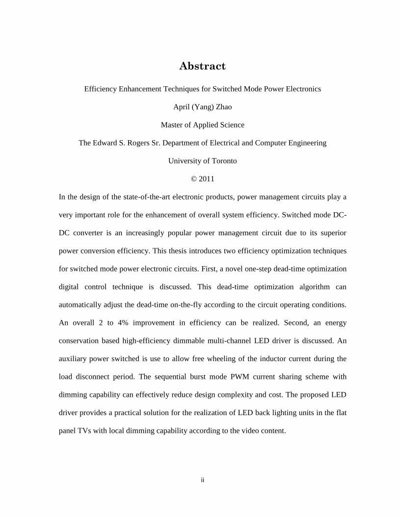
frequencies. We note that the power loss can easily exceed a few watts. Figure 2.3 shows
the power saving by the elimination of body-diode conduction loss and reverse recovery
loss. Percentage power saving is defined as the ratio between power loss and output
power. The power saving due to the elimination of body-diode conduction (%Psav_con) is
approximated based on 10 ns body-diode conduction time (td) on both rising and falling

9
edge. The power saving due to the elimination of reverse recovery loss (%Psav_rr) is
approximated based on 15 nC reverse recovery charge (Qrr), 5 V supply voltage (Vg) and
5 A output current (Iout). The calculation is as following:
ds
out
F
out
Dconsav tf
V
V
P
PP 2% _ (1.1)
s
outout
grr
rrsav fVI
VQP
2% _ (1.2)
They are plotted with solid and dot lines on the graph. It can be seen that with the
increase of switching frequency and reduction of output voltage, power saving can be
significantly increased. This is because the ratio between body-diode voltage drop and
output voltage increases with decreasing of output voltage. Hence, dead-time
optimization is most important in applications requiring low output voltage and high
switching frequency.

10
Figure 2.2: Cross-conduction power loss approximation for different supply voltages and
operating frequencies.
0
10
20
30
40
50
0 2 4 6 8 10 12 14
Po
wer
Lo
ss (
w)
Vin (V)
Cross-conduction Power Loss
fsw = 1.2MHz
fsw = 1MHz
fsw = 800KHz
fsw = 600KHz
Figure 2.1: Timing diagram showing the relationship between the MOSFETs DPWM
signals and the actual gate driving signals
(a) Optimum dead-time resulting in completely elimination of cross conduction
and no body- diode conduction occurred.
(b) Excessively long dead-time will cause body-diode conduction during
switching transient.
DTfall DTrise DTfall
HS DPWM
LS DPWM
HS Gate Driving Signal
LS Gate Driving Signal
DTrise
(a) (b)
11
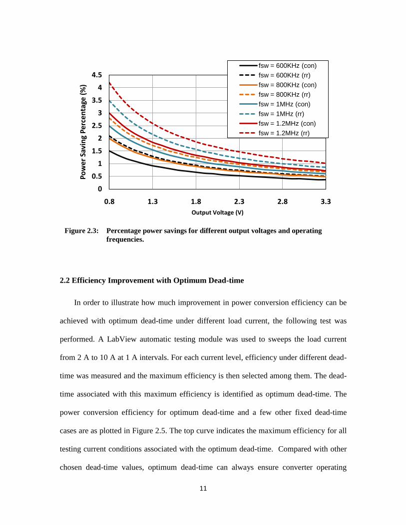
2.2 Efficiency Improvement with Optimum Dead-time
In order to illustrate how much improvement in power conversion efficiency can be
achieved with optimum dead-time under different load current, the following test was
performed. A LabView automatic testing module was used to sweeps the load current
from 2 A to 10 A at 1 A intervals. For each current level, efficiency under different dead-
time was measured and the maximum efficiency is then selected among them. The dead-
time associated with this maximum efficiency is identified as optimum dead-time. The
power conversion efficiency for optimum dead-time and a few other fixed dead-time
cases are as plotted in Figure 2.5. The top curve indicates the maximum efficiency for all
testing current conditions associated with the optimum dead-time. Compared with other
chosen dead-time values, optimum dead-time can always ensure converter operating
Figure 2.3: Percentage power savings for different output voltages and operating
frequencies.
0
0.5
1
1.5
2
2.5
3
3.5
4
4.5
0.8 1.3 1.8 2.3 2.8 3.3
Po
wer
Sav
ing
Per
cen
tage
(%
)
Output Voltage (V)
fsw = 600KHz (con)
fsw = 600KHz (rr)
fsw = 800KHz (con)
fsw = 800KHz (rr)
fsw = 1MHz (con)
fsw = 1MHz (rr)
fsw = 1.2MHz (con)
fsw = 1.2MHz (rr)

12
without any cross-conduction and body-diode conduction loss, achieving higher
efficiency. Based on the testing data collected, it is observed the optimum dead-time
varies with current level.
Figure 2.5: Power conversion comparison for different dead-times.
82%
84%
86%
88%
90%
92%
0 2 4 6 8 10 12
Eff
icie
nc
y (
%)
Output Current (A)
Deadtime -10ns
Deadtime 0ns
Deadtime 10ns
Deadtime 25ns
Optimum Deadtime
Figure 2.4: Experimental setup for optimum dead-time identification.

13
In the following sections, a one-shot dead-time correction algorithm that can achieve
optimum dead-time operation under all loading current conditions will be described.
2.3 Literature Review
The optimum dead-time varies with circuit parameters, operation conditions and
temperature. Traditional DC-DC converters use fixed dead-time control scheme. It
applies a sufficiently long dead-time to cover the entire operating range. This means that
the dead-time is not optimized for certain current. In order to address the switching delay
that exists between the DPWM signal and the turning on and off of the power MOSFETs,
many design techniques have been proposed to provide on-the-fly dead-time adjustment
for different MOSFETs and accommodate temperature variations [2], [3].
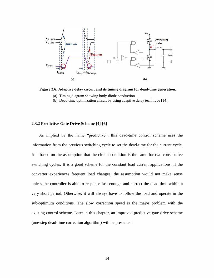
2.3.1 Adaptive Delay Technique [2]
Adaptive delay control scheme is a commonly used technique. Figure 2.6 shows one
possible implementation of this scheme. The major drawback is that the instant when the
MOSFETs turn-on is determined by sensing the zero crossing at the switching node. This
fails to take into account the gate charging time, therefore by the time the MOSFETs turn
on, the LS MOSFET body-diode already starts to conduct. In addition, the logic gates
also introduce propagation delays to the actual dead-time.
14
2.3.2 Predictive Gate Drive Scheme [4]-[6]
As implied by the name “predictive”, this dead-time control scheme uses the
information from the previous switching cycle to set the dead-time for the current cycle.
It is based on the assumption that the circuit condition is the same for two consecutive
switching cycles. It is a good scheme for the constant load current applications. If the
converter experiences frequent load changes, the assumption would not make sense
unless the controller is able to response fast enough and correct the dead-time within a
very short period. Otherwise, it will always have to follow the load and operate in the
sub-optimum conditions. The slow correction speed is the major problem with the
existing control scheme. Later in this chapter, an improved predictive gate drive scheme
(one-step dead-time correction algorithm) will be presented.
Figure 2.6: Adaptive delay circuit and its timing diagram for dead-time generation.
(a) Timing diagram showing body-diode conduction
(b) Dead-time optimization circuit by using adaptive delay technique [14]

15
2.3.3 Dead-time Search Algorithm
Dead-time search algorithm [7] is based on the idea that optimum dead-time always
gives the highest efficiency. The optimum dead-time is identified through sequentially
changing rising edge and falling edge dead-time and efficiency capturing. Depending on
the initial dead-time value and circuit condition, this method may require many switching
cycles to obtain the optimum dead-time. Slow correction speed also renders this method
unsuitable for applications with frequently changing loads.
2.4 Optimum Dead-time Functional Mechanism
In order to determine the length of optimum dead-time, the turn-on and turn-off
instants at the switching node are analyzed. Figure 2.7 shows the gate driving signal
switching diagram for three dead-time cases. The critical transition instant is analyzed in
one switching cycles during steady-state. Figure 2.7(a) illustrates the optimum dead-time
case. From the beginning of the switching cycle, after the LS gate turns off, the LS
MOSFET will experience certain delay td1 before it is completely turns off. If the HS
MOSFET just turns on at that moment, the switching node voltage Vswi will go high and
remain high until the HS gate turns off. After certain delay td2, the HS MOSFET will be
completely turned off and starts to discharge the switch node parasitic until reach ground
level. If the LS MOSFET just turns on at that instant, it will take over the inductor current
and switching node will be kept clamped to ground level. Figure 2.7(b) shows the
switching diagram for excessively long dead-time case. This happens when one of the
MOSFET already fully turn-off, but the other MOSFET has not yet start to conduct. It
could occur in the duration between the LS MOSFET turn-off and the HS MOSFET turn-

16
on or between the HS MOSFET turn-off and the LS MOSFET turn-on. In the case of late
turn-on, both MOSFETs are off and inductor current cannot flow though the intended
path. Since the current flow cannot be disrupted, the inductor current will flow through
the LS MOSFET’s body-diode, resulting in higher conduction loss and subsequent high
reverse recovery loss. Figure 2.8 shows the current flow. Figure 2.7(c) shows the case
with insufficient dead-time. This happens when one of the MOSFET already start to
conduct before the other MOSFET fully turns off, resulting in unwanted shoot through
current. Figure 2.9 shows the current flow.
When the critical turn-on moment is not met, unnecessary conduction loss will be
incurred. The proposed one-step dead-time correction algorithm is designed to capture
this critical switching instant and ensure no dead-time related loss is induced in the
system.

17
Figure 2.7: MOSFET switching diagrams for optimum, long and short dead-time cases.
HS Vgate
td1
tdisc
Vswi
HS
Turn on
LS
Turn on
No body-diode conduction or cross conduction
occurs at both rising edge and falling edge
LS Vgate
HS Vgate
td2
(a)
(b)
td1
tdisce
Vswi
Delayed HS
Turn on
Delayed LS
Turn on
Body-diode conduction
at the rising edge
Body-diode conduction
at the falling edge
LS Vgate
HS Vgate
td2
Vswi
Earlier HS
Turn on
Earlier LS
Turn on
LS Vgate
(c)
Cross conduction
at the rising edge
Cross conduction
at the falling edge
(a) Switching diagram for optimum dead-
time condition
(b) Switching diagram for excessively long
dead-time condition
(c) Switching diagram for insufficient
dead-time condition

18
c
VinVdd
Vdd
Dead-time
is too short
C
L
Lo
ad
ON
ON
Figure 2.9: Current flow through Vdd to ground when dead-time is too short.
VinVdd
Vdd
Dead-time
is too long
C
L
Lo
ad
OFF
OFF
Figure 2.8: Current flow through LS MOSFET body-diode when dead-time is too long.

19
2.5 Overall Operation
The block level diagram of the optimum dead-time control system is as shown in
Figure 2.10. The shaded block on the left side shows the digitally implemented dead-time
correction algorithm, which consists of a pulse width measurement module, an optimum
dead-time generator module and a hybrid DPWM module. The buck converter output
stage with body-diode detection circuit (NOR gate) is as shown on the right side. The
output stage was implemented using discrete components on PCB. The optimum dead-
time control system operates as follows: the body-diode conduction detection circuit
monitors the gate-source voltage (Vgate-low) and the drain-source voltage (Vsw-node) of the
LS power MOSFET. Whenever body-diode conduction is detected, a pulse will be
generated and pass onto the pulse width measurement module in the digital controller.
The conduction pulse width is proportional to the duration of the body-diode conduction
time. It can be measured with a resolution of 1.25 ns. This produces a 5 bits digital signal
for the optimum dead-time generator. Based on the body-diode conduction time
measurement and the current dead-time values, the optimum dead-time is then calculated,
and the hybrid DPWM module will generate the appropriate HS and LS DPWM signals
in next switching cycle.

20
2.6 System Function Module Description
Since this work mainly focuses on the optimum dead-time and DPWM signal
generation, only the digital control modules, including a dead-time correction module, a
body-diode conduction measurement module and a DPWM generation module, will be
elaborated in this section. All the digital modules are coded in Verilog, and are
implemented using the standard cell approach. The design flow is automated using
synthesis tools and automatic place & route tools with additional timing constrains.
Power converter output stage is using an existing design with small modifications to
accommodate the body-diode detection circuit. In Section 2.6.2, discussion regarding the
realization of body-diode conduction detection circuit will be provided. Output stage
design specifications will be provided in Section 2.6.5.
Figure 2.10: System level diagram of the implement of one-step dead-time correction
algorithm.
Vin
L
C Load
Vsw_node
Digital Controller
HS
MOSFET
LS
MOSFET
HS
Gate Driver
LS
Gate Driver
Conduction pulse Clk_25MHz
h
BD1[4:0]
DPWM
modulator
Pulse Width
Measurement
Optimum Dead-
time Generator
DT1 [9:0] Vgate_low
VNOR_detect

21
2.6.1 One-step Dead-time Correction Algorithm
The flow chart for the proposed one-step dead-time correction algorithm is as shown
in Figure 2.11. For simplicity, the correction procedure will be demonstrated on the HS
DPWM rising edge only. The algorithm begins by measuring the actual body-diode
conduction time and then changes the dead-time to the optimum value in the next
switching cycle. It operates in three steps as described below:
Step 1: initial dead-time value assumption
The algorithm starts with an initial safe dead-time value (DTrise_ini) pre-programmed
into the digital controller. Since the power line to ground cross-conduction induces more
power loss and can introduce severe damage to the power stage, a sufficiently long dead-
time should be used at the start of the circuit. In this case, we already aware of the
optimum dead-time value to be around 3 ns from the previous testing. Therefore, 5 ns
was chosen as the initial safe dead-time. In the case where no prior knowledge of the
circuit characteristics is available, an excessively long dead-time, such as 20 ns or 30 ns
may also be used. Although a long dead-time, DTrise_ini may degrade the power
conversion efficiency initially, the proposed correction algorithm can always update the
dead-time to the optimum value in the next switching cycle. Hence the severe body-diode
conduction loss in the previous cycle will not propagate into the subsequent cycles.

22
Step 2: Body-diode conduction detection
During the transitions (0-1 and 1-0) of the HS DPWM signal, a NOR gate senses the
gate-source voltage Vgate-low and the drain-source voltage Vsw-node from the LS power
MOSFET. Whenever there is a delay between the transitions of these two signals, body-
diode conduction is assumed [3]. This function will be elaborated in Section 2.6.2.
Step 3: Body-diode conduction time measurement
This body-diode conduction time is the excess dead-time that needs to be measured
and subtracted from the current dead-time values. The process will be elaborated in
Section 2.6.3.
Figure 2.11: A flow chart representation of the one-step dead-time optimization
algorithm.

23
Step 4: Optimum dead-time update
The optimum dead-time update is done digitally via a subtraction circuit in the
FPGA implementation. The new dead-time is then used to update the DPWM signals for
the next switching cycle.
As mentioned in Section 2.4, the dead-time could be optimum, too short, or too long.
The NOR gate detection circuit that monitors Vgate-low and Vsw-node is used to detect this
difference. A zero output from the NOR gate may indicate either (1) the dead-time is too
short or (2) optimum dead-time is obtained. Under this situation, the controller will
increase the dead-time by 1-bit in the next cycle. In case (1), dead-time will continuously
increase until the optimum value is obtained. Case (2) implies that the system is operating
at the cross-conduction boundary, dead-time dithers within a 1-bit window. Finer
adjustment of the dead-time ensures the maximization of conversion efficiency. This
optimization method is independently applied to both the turn-on and turn-off edge of the
gate drive signals.
2.6.2 Body-diode Conduction Detection Circuit
The presence of body-diode conduction in the LS power MOSFET is an indication of
excessively long dead-time. A simple way to detect body-diode conduction is to monitor
the voltages Vsw-node and Vgate-low. As shown in Figure 2.12(a), under ideal condition, the
LS power MOSFET should be turned on as soon as the HS power MOSFET is turned off
(causing Vsw-node to go low). If this is not the case, the inductor current will flow through
the LS MOSFET body-diode, resulting in unwanted conduction loss. Moreover, when the
LS power MOSFET is turned on, and if the voltage drop across it is less than VF
(synchronous rectifier body-diode’s forward voltage drop), it will force the body-diode to
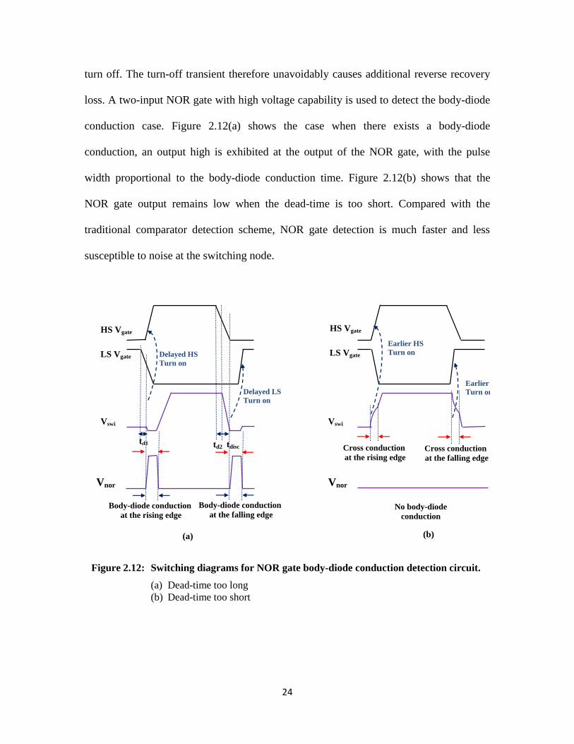
24
turn off. The turn-off transient therefore unavoidably causes additional reverse recovery
loss. A two-input NOR gate with high voltage capability is used to detect the body-diode
conduction case. Figure 2.12(a) shows the case when there exists a body-diode
conduction, an output high is exhibited at the output of the NOR gate, with the pulse
width proportional to the body-diode conduction time. Figure 2.12(b) shows that the
NOR gate output remains low when the dead-time is too short. Compared with the
traditional comparator detection scheme, NOR gate detection is much faster and less
susceptible to noise at the switching node.
Figure 2.12: Switching diagrams for NOR gate body-diode conduction detection circuit.
(a) Dead-time too long
(b) Dead-time too short
tdisc
Vnor
No body-diode
conduction
detected
Body-diode conduction
at the falling edge
td1
Vswi
Delayed HS
Turn on
Delayed LS
Turn on
LS Vgate
HS Vgate
td2
HS Vgate
Vswi
Earlier HS
Turn on
Earlier LS
Turn on
LS Vgate
(b)
Cross conduction
at the rising edge
Cross conduction
at the falling edge
(a)
Vnor
Body-diode conduction
at the rising edge
25
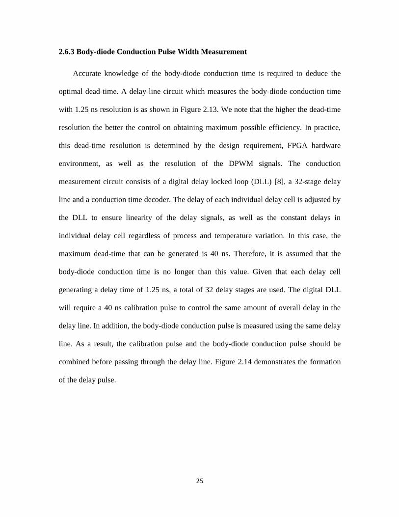
2.6.3 Body-diode Conduction Pulse Width Measurement
Accurate knowledge of the body-diode conduction time is required to deduce the
optimal dead-time. A delay-line circuit which measures the body-diode conduction time
with 1.25 ns resolution is as shown in Figure 2.13. We note that the higher the dead-time
resolution the better the control on obtaining maximum possible efficiency. In practice,
this dead-time resolution is determined by the design requirement, FPGA hardware
environment, as well as the resolution of the DPWM signals. The conduction
measurement circuit consists of a digital delay locked loop (DLL) [8], a 32-stage delay
line and a conduction time decoder. The delay of each individual delay cell is adjusted by
the DLL to ensure linearity of the delay signals, as well as the constant delays in
individual delay cell regardless of process and temperature variation. In this case, the
maximum dead-time that can be generated is 40 ns. Therefore, it is assumed that the
body-diode conduction time is no longer than this value. Given that each delay cell
generating a delay time of 1.25 ns, a total of 32 delay stages are used. The digital DLL
will require a 40 ns calibration pulse to control the same amount of overall delay in the
delay line. In addition, the body-diode conduction pulse is measured using the same delay
line. As a result, the calibration pulse and the body-diode conduction pulse should be
combined before passing through the delay line. Figure 2.14 demonstrates the formation
of the delay pulse.

26
The formation of delay pulse is essentially a superposition process implemented
digitally by an OR gate. The resulting delay pulse contains two parts of information, one
is the 40 ns calibration pulse and the other is the body-diode conduction pulse.
As the delay pulse travels along the delay-line, each delay tap will contribute 1.25 ns
delay. The delay line will generate 32 delayed input delay pulses in total and they are
sampled at the falling edge of the body-diode conduction pulse. This delay line
Figure 2.14: Timing diagram shows the formation of delay pulse.
Figure 2.13: Body-diode conduction pulse width measurement using a delay line and
delay lock loop.
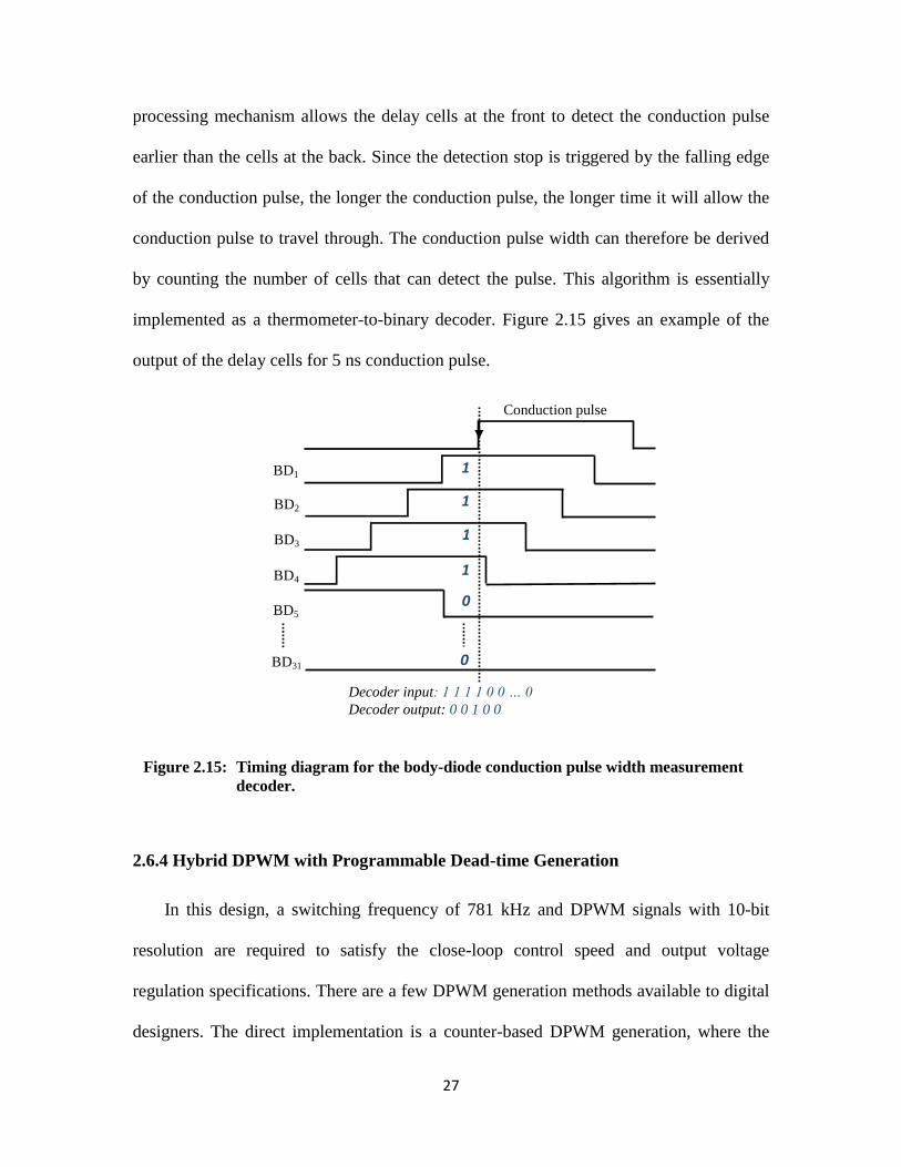
27
processing mechanism allows the delay cells at the front to detect the conduction pulse
earlier than the cells at the back. Since the detection stop is triggered by the falling edge
of the conduction pulse, the longer the conduction pulse, the longer time it will allow the
conduction pulse to travel through. The conduction pulse width can therefore be derived
by counting the number of cells that can detect the pulse. This algorithm is essentially
implemented as a thermometer-to-binary decoder. Figure 2.15 gives an example of the
output of the delay cells for 5 ns conduction pulse.
2.6.4 Hybrid DPWM with Programmable Dead-time Generation
In this design, a switching frequency of 781 kHz and DPWM signals with 10-bit
resolution are required to satisfy the close-loop control speed and output voltage
regulation specifications. There are a few DPWM generation methods available to digital
designers. The direct implementation is a counter-based DPWM generation, where the
Figure 2.15: Timing diagram for the body-diode conduction pulse width measurement
decoder.
Conduction pulse
BD5
BD4 1
BD3
1 BD2
1 BD1
1
0
BD31
0
Decoder input: 1 1 1 1 0 0 … 0
Decoder output: 0 0 1 0 0

28
counter clock frequency is directly dependent on the number of bits in the DPWM signal.
In our case, a 210
× 781 kHz = 0.8 GHz counter clock is required. In practice, higher
clock frequency requirement makes the DPWM implement a difficult task. Another
common approach is the delay-line based DPWM. However, longer delay-line associated
with higher DPWM resolution requires larger chip area and also more susceptible to
process and temperature variations. Although other novel DPWM generation methods,
including dithering and sigma-delta modulation can be used to improve the effective
DPWM resolution to some extent, they both require relatively large hardware resources.
In this work, a 5-bit counter and 5-bit delay-line based hybrid DPWM topology is
used to provide a practical trade-off between the high clock frequency requirements of
counter-based DPWMs and the large hardware requirements of delay-line based DPWMs
[9]. Digital delay-locked loop is also utilized to adjust the delay of each delay cell in
order to improve the linearity of the resulting DPWM signal.
The delay of each delay cell should be designed to be adjustable in order to
accommodate process and temperature variations. Unlike analog delay cell realization,
where delay can be calibrated through the supply voltage, digital delay cell implemented
by FPGA do not have the capability to adjust the power supply level. In each digital
delay cell, multiple delay paths are pre-designed to have delays varied around the
nominal value. Depending on the circuit condition, a digital DLL circuit selects the delay
path in each delay cell, such that the desired overall delay time and linearity are satisfied.
In this work, each delay cell consisting two delay paths with 0.9 ns and 1.35 ns delay is
used to ensure an average of 1.25 ns delay. Figure 2.16 shows the schematic construction
of each delay cell. It can be noted that by implementing multiple delay paths with small

29
incremental changing delays in each delay element, better linearity can be achieved. For
simplicity, 2 delay paths are used in our case.
As shown in Figure 2.17, each delay element in the delay path is constructed by
using two two-input NOR gates. Each delay element generates a delay of 0.4 ns. Based
on the Verilog synthesize measurement, the longer delay path has a propagation delay of
1.35 ns and that for the shorter delay is 0.9 ns.
As for the DPWM modulation schemes, there are leading edge, trailing edge and
triangular DPWM modulation [9]. The only difference among these schemes is in the
combinational logic that provides the counter and delay line timing. The discussion in
this Section will be based on trailing edge DPWM modulation, where the starting point of
Figure 2.17: Schematic of the delay element.
Delay
element Two-input
NOR Gate
Figure 2.16: The construction of 1.25ns delay cell with 2 delay paths.
Input Pulse
Path Select
output
Delay
element

30
output high is fixed and this is the instant when the counter reach its maximum count (at
the beginning or the end of every switching cycle).
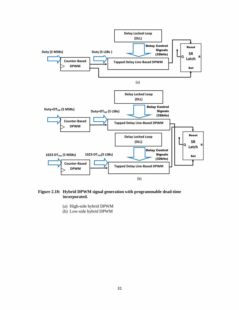
Figure 2.18 shows the circuit used to generate the hybrid DPWM signals. For both
HS and LS generation schemes, the SR latch is used to set the digital levels of the
corresponding DPWM signals. In particular, the output of SR latch goes high when the
rising edge of Set signal is triggered, and goes low when the rising edge of Reset signal is
triggered. The preceding 5-bit counter and 32-stage delay line are used to process the Set
and Reset trigger timing of the SR latch. Figure 2.19 shows the timing diagram of the HS
and LS DPWM signal generation with programmable dead-time control. Since the
trailing edge scheme is applied, the rising edge of the HS DPWM shall always starts from
the beginning of each switching cycle, with 0 indicating the Set trigger timing and duty
value indicating the Reset trigger timing in the HS SR latch. Also, for the LS DPWM, the
Set trigger timing is D + DTfall and Reset trigger timing is 1023 DTrise.
31
Figure 2.18: Hybrid DPWM signal generation with programmable dead-time
incorporated.
(a) High-side hybrid DPWM
(b) Low-side hybrid DPWM
Delay Control
Signals
(32bits)
Delay Control
Signals
(32bits)
Delay Control
Signals
(32bits)
Tapped Delay Line-Based DPWM
SR Latch
R
Reset
Set
Duty (5 MSBs) Duty (5 LSBs )
Q
Delay Locked Loop
(DLL)
Counter-Based
DPWM
SR Latch
R
Reset
Set
Duty+DTfall (5 MSBs) Duty+DTfall (5 LSBs)
Q
Delay Locked Loop
(DLL)
Counter-Based
DPWM
1023-DTrise (5 MSBs) 1023-DTrise(5 LSBs)
Delay Locked Loop
(DLL)
Counter-Based
DPWM
Tapped Delay Line-Based DPWM
Tapped Delay Line-Based DPWM
(a)
(b)

32
2.6.5 Output Stage Design Specifications
The proposed one-step dead-time optimization algorithm is tested on an existing
output stage PCB designed by Kendy Ng (a former graduate student). The output stage
PCB layout and design parameters are as shown in Figure 2.20 and Table 2.1.
Figure 2.19: Timing diagram of HS and LS DPWM signal generation with programmable
dead-time.
HS DPWM
LS DPWM
DTfall DTrise
1 Switching Cycle
Duty
Set
Reset
0
Duty
0
Duty+DTfall
Set
Reset
1023-DTrise
DTrise
1023

33
Figure 2.20: Output stage PCB layout.

34
2.7 Experimental Results
The proposed one-step dead-time correction algorithm is verified experimentally in
both steady-state and load transient conditions. The testing is performed by using an
FPGA implementation for the controller and discrete output power MOSFETs with gate
driver ICs. (The PCB layout was presented in Section 2.6.5).
2.7.1 Conversion Efficiency during Steady-state
Dead-time correction algorithm is first tested under constant current conditions.
Figure 2.21 shows the waveform for non-optimum dead-time case when converter is
delivering a load current of 2 A. V_NOR(detect) is the output of NOR gate, signalling the
presence of body-diode conductions. V_NOR(test) is the re-shaped V_NOR(detect) pulse
Table 2.1: Summary of design parameters for a 6 V to 1 V DC-DC buck converter
Components Abbreviation Value Model Comment
Output
capacitor Cout 100 µF GRM31CF50J107ZE01L ESR = 4 mΩ
Inductance L 2.2 µH PCMC063T Rdc = 2.8 mΩ
Power
MOSFETs MOSFET IRF7821
Gate
driver GD TC4426
Propagation
delay = 30 ns
8-bit
ADC ∆ADC 3.9 mV PCMC063T Rdc = 20 mΩ
DPWM
resolution DPWM 8 bits

35
after passing through two inverters to restore logic levels. Figure 2.22 shows the body-
diode conduction is eliminated when the dead-time correction algorithm is applied.
Steady-state efficiency is then measured under this condition. Similar tests are conducted
for load current varying from 0.5 A to 10 A at 0.5 A interval. Experimental results
(Figure 2.23) show that with the body-diode conduction eliminated, the power conversion
efficiency is improved by 2% to 4%.
Figure 2.21: The NOR gate body-diode conduction detection waveform (steady-state)
shows a non-optimum dead-time condition.

36
Figure 2.23: Power conversion efficiency is increased by 2% to 4% compared with non-
optimum dead-times case.
Figure 2.22: Body-diode conduction detection waveform (steady-state) shows body-diode
condition is eliminated with dead-time correction algorithm.

37
2.7.2 Conversion Efficiency during Load Transient
Different converter close loop control schemes have different dynamic characteristic,
therefore transient response time largely depends on the topologies of the controller, as
well as design specifications. In modern controller designs, such as PID, PI, hysteretic
controllers [10], the converter usually requires a few switching cycles to reach stead-state,
especially after a large load transient. In order to eliminate the influence of the various
controllers, the conversion efficiency during load transient is tested under open loop
conditions.
Figure 2.24 shows the existence of body-diode conduction with the change of load.
When the load_change signal is activated, the load current is changed from 0.1 A to 4 A.
As the inductor current starts to rise, body-diode conduction begins to appear. The
gradual change of the inductor currents requires different optimum dead-time for each
current level. In this case, as the output current increases, shorter dead-times are required.
However, in this part of the experiment, the dead-time is fixed. As a result, the LS
switch’s body-diode starts to conduct. The body-diode conduction time also gradually
increases as the inductor current rises slowly to the new load current. In order to show the
gradual change in body-diode conduction upon reaching steady state, the oscilloscope
capture time scale is set at 2 µs/div. Figure 2.25 is a closed-up view at the 14th
switching
cycle, counted from the beginning of the load_change activated.

38
Figure 2.24: Switching waveforms show that body-diode conduction gradually increases
when current experiences a sudden increase from 0.1A to 4A eliminated with
dead-time correction algorithm.
14 switching cycle

39
The gradual change in the inductor current for the same 0.1 A to 4 A load change is
as shown in Figure 2.26. The amount of time required to reach the new steady state is
approximately 20 switching cycles. This verifies the observation of the progressive
appearance of the body-diode conduction after the load change in Figure. 2.26. With the
Optimum Dead-time Generator activated the switching waveforms in Figure. 2.27 shows
that body-diode conduction can always be eliminated during and after the load change.
In comparison with other slow dead-time searching algorithm, multiple switching
cycles may be required to response to the current load condition, which makes it very
unsuitable for frequent load change applications. Moreover, when the system is operated
in close loop, the transition time will be reduced depending on particular control scheme.
Figure 2.25: A close-up view of the body-diode conduction at the 14th switching cycle after
the load current starts to change

40
However current variation still exists for certain period of time, and the optimum dead-
times are also needed to ensure the conversion efficiency during load change.
Figure 2.26: The inductor current waveform increases gradually during a load change
from 0.1 A to 4 A.

41
2.8 Conclusion
Dead-time optimization is one the techniques to improve the efficiency in a power
management system. This chapter discussed the implantation and verification of a
proposed one-step dead-time correction algorithm. The proposed method can detect and
measure body-diode conduction and optimize the dead-time on the fly. In addition to the
elimination of body-diode conduction loss, the reverse recovery loss is completely
avoided since the body-diode never becomes fully saturated. This method successfully
avoids the drawbacks of many existing dead-time control schemes. It constantly
optimizes the dead-time during any load condition such that the maximum possible
Figure 2.27: Switching waveforms show that body-diode conduction is eliminated with
dead-time correction algorithm.

42
conversion efficiency is always ensured. A higher switching frequency can therefore be
used due to the significant reduction of power dissipation. As a result, the further
minimization of output stage becomes possible.
43
CHAPTER 3
An Energy Conservation Based High-efficiency Dimmable
Multi-channel LED Driver
This chapter presents a high-efficiency multi-channel LED back-lighting units (BLU)
driver for LCD panel with local dimming capability. A sequential burst-mode channel
multiplexed pulse width modulation dimming scheme is introduced to regulate and
maintain uniform LED current. An energy conservation technique is utilized to handle
load disconnect situation, which significantly improves the efficiency over the entire
dimming range. The proposed approach completely eliminates the dedicated linear
current regulator and sensing components in each LED channel as required by recently
reported methods. This work is well suited for digital IC implementation for dynamic
LED luminance adjustment. The performance of the proposed method was verified
experimentally using a 4.5 V to 14 V boost converter. An overall efficiency of 50-90%
was observed over a wide range of LED luminance. The following sections describe the
importance of local dimming, existing LED driver topology and the circuit realization of
a 4 3 LED driver.

44
3.1 Back-lighting Units with Local Dimming for Flat Panel Displays
LED BLUs are rapidly taking over the traditional cold cathode florescent lights
(CCFL) and becoming the major LCD flat panel back-lighting technology. This is due to
the distinct performance and advantages of LEDs, such as high optical efficiency and
long operating life. In addition, LED BLU allows more flexibility in terms of locally
dimming individual LEDs depending on video/picture content. Traditional LCD CCFL
BLUs provide uniform luminance to the LCD panel. Depending on the image content, the
LCD display controller regulates the voltage on thin-film-transistor (TFT) at each pixel to
change the orientation of the liquid crystal. The orientation angle of the liquid crystal
determines the amount of light allowed to pass through each pixel on the LCD panel. For
example, an orientation of 90o blocks the light from the BLU entirely. An orientation of
0o allows the light to pass through completely, and any angles in-between allows the back
light to partially pass through the panel. However the liquid crystals can never completely
block the light due to the light leakage [11]-[13]. This inherent physical limitation of
LCD makes true black display and high BW (black and white) contrast ratio very
challenging. An effective solution to improve contrast ratio is to dynamically adjust LED
back light luminance (local dimming). This can be achieved by dividing the LED BLU
panel into a number of small regions LED brightness in each region is regulated
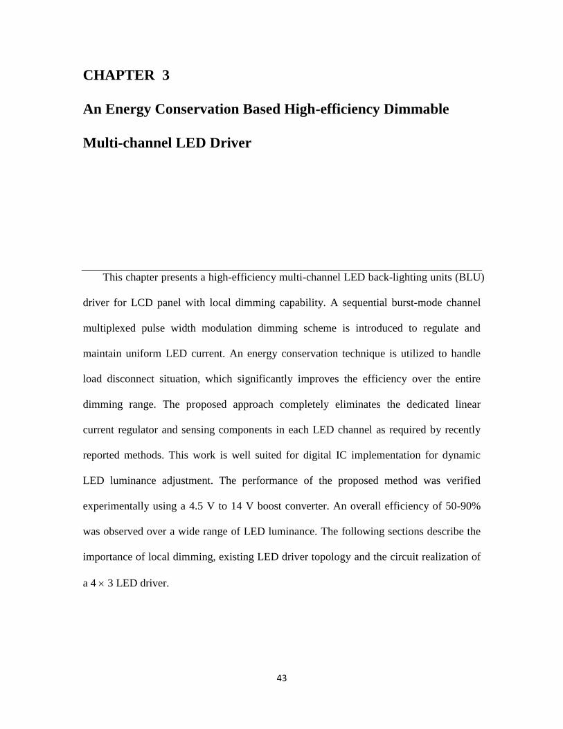
individually according to the image content in that region. Figure 3.1 shows a structure of
flat panel LCD unit with local dimming capabilities.
45
3.2 Literature Review
The luminance of an LED is directly proportional to its current. The LED driver is
essentially a current regulator. Various circuit techniques utilizing current regulator
(linear or switched mode) have been proposed for driving parallel connected LED strings.
Linear regulator offers a simpler and low cost solution while switched mode converter
offers a more complex but more power efficient solution. A straight forward approach is
to employ a linear current regulator for each LED string. This offers precise current
regulation, but efficiency decreases at higher difference between the input and output
voltages. Some LED driver topologies utilize a combination of linear and switched mode
regulators, which providing the advantages of both cost and efficiency. In this case, the
LED string voltage is typically powered by a switched mode voltage pre-regulator, and
LED Back Lighting
LCD TFT
Screen
Figure 3.1: The luminance of LED can be dynamically adjusted according to image
content.

46
the LED string current is individually regulated by linear regulators. In order to optimize
efficiency, the output of pre-regulator is often set at the lowest possible level to ensure
proper operation of the linear regulators. Sensing techniques have to be used to achieve
this goal. This idea was implemented in similar ways in self-adaptive drives as reported
in [14] and [15]
3.2.1 Self-adaptive Drives [14]
As shown in Figure 3.2, the output voltage of the pre-regulator is always self-
adjusted such that the voltage across the linear current regulator of the LED string with
the highest voltage drop is kept at the minimum value to reduce power loss. The
drawback of this approach is that the efficiency is strongly affected by the selection of the
reference voltage.
Figure 3.2: LED driver with adaptive drive voltage for linear current regulator.

47
3.2.2 One-comparator Counter Based Inductor Current Sampling Method
The one-comparator counter based inductor current sampling method [16] as shown in
Figure 3.3 is implemented in a 6-phase LED driver. In this method, a comparator is used
to regulate the maximum allowed inductor current of each phase in order to eliminate the
need of using ADC as in conventional sampling method. The LED current information of
the 6 phases can be sequentially captured by comparing the inductor current with the
preset reference current value. A counter is used in this method to control the timing of
the detection sequence such that the corresponding close loop PID controller of each
phase can be activated for LED current regulation. However, this method requires one
converter to control each string of LEDs, which unavoidably increases system cost,
especially in multi-string LED applications. Also the inductor current sampling is only
valid in converters where the load current equals to the inductor current. In boost
converters, the LED load current also depends on the duty cycle, which makes this
method not readily applicable.

48
The aforementioned approaches use analog current dimming methods. Analog
diming is a straightforward method to change LED brightness by adjusting its forward
biased current. The main drawback is color shift and color temperature change with
varying current level. Burst mode PWM dimming has proven to be an effective approach
Figure 3.3: A representation of the one-comparator counter based inductor current
sampling method.

49
to avoid those problems in analog dimming. It is realized by keeping the LED current
constant and regularly disconnecting the LED string depending on the dimming ratio.
The PWM dimming signal is typically in the 100 - 400 Hz range. Section 3.2.3 discusses
a recently published high frequency PWN dimming method.
3.2.3 High Frequency PWM Dimming
In conventional PWM MOSFET series dimming, a sense resistor and a dimming
MOSFET is connected in series with the LED string as shown in Figure 3.4. The output
voltage is regulated by the close-loop controller to maintain a nominal constant LED
current. The dimming MOSFET can be turned on and off to control the connection time
of the LED string. The luminance of the LED is determined by the averaged output
current. The main difficulty in the controller design is during the dimming MOSFET off
time. During this period, since the load is disconnected and the voltage of sense resistor
drops to 0, the control loop will tend to infinitely increase the output voltage. When
dimming MOSFET turns on, very high current will flow through LED string resulting in
luminance flickering or even physical damage to the components. Gacio et al. used a very
high dimming frequency (over 100 kHz) to avoid the control loop design difficulties. The
LEDs are dimmed at frequencies far beyond the close-loop cut-off frequency. Since the
controller is only able to compensate the load change slower than the cut-off frequency,
the high frequency load disconnect will not disrupt the function of the controller. In this
case, the constant LED current during the PWM on-time is ensured. However, higher
dimming frequency leads to higher switching loss. Also since dimming period is much
reduced, the dimming delay portion in the dimming cycle becomes significant. This leads
to low contrast ratio.

50
3.3 System Operation
The proposed LED back-lighting system is as shown in Figure 3.5. It consists of a
flat panel active TFT matrix LCD screen, the LED BLU, the LED drivers, LCD display
control and BLU control unit. The system is built based on an existing 17’ LCD monitor,
the LED BLU, LED driver panel and BLU control unit are designed in this work. The
following sections in this chapter will focus on the development of these three modules.
PWM
Dimming signal
Rsen
LED Current
Vout
Dimming
MOSFET
Figure 3.4: High frequency series PWM dimming

51
The LED BLU is responsible for providing back light to the LCD panel. The
particular panel used in this experiment has a dimension of 17 inch diagonally and with
an aspect ratio of 4:3. The LED BLU is positioned directly behind the LCD panel. There
are 48 LED mounted on the BLU with equal spacing in between. The LED BLU is
divided into 12 identical regions, each region contains 4 LEDs. The 12 region can be
grouped in to 4 columns, each column contains 3 regions.
The driver unit contains 4 multi-channels LED drivers, with each driver controlling
one column of region in LED BLU. The luminance of each region in every column is
adjusted by the PWM dimming signals applied to the corresponding LED driver.
The BLU control unit consists of a video processing module and a LED driving
signal generator module. The video processing module is responsible for analyzing the
video/image content and calculating the necessary LED luminance levels for each region.
DVI
LED BLU
LCD TFT
screen
LCD display
Controller
LED drivers
Video Processing
Module
Multi-channel LED
Driver signals
BLU Control unit
Figure 3.5: A block diagram of the proposed LED back-lighting system consisting of a flat
panel active TFT matrix LCD screen, the LED BLU, the LED drivers panel,
LCD display control and BLU control unit.
52
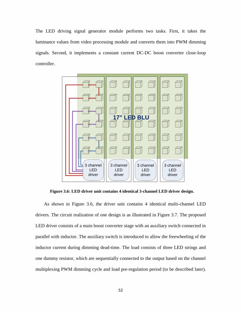
The LED driving signal generator module performs two tasks. First, it takes the
luminance values from video processing module and converts them into PWM dimming
signals. Second, it implements a constant current DC-DC boost converter close-loop
controller.
As shown in Figure 3.6, the driver unit contains 4 identical multi-channel LED
drivers. The circuit realization of one design is as illustrated in Figure 3.7. The proposed
LED driver consists of a main boost converter stage with an auxiliary switch connected in
parallel with inductor. The auxiliary switch is introduced to allow the freewheeling of the
inductor current during dimming dead-time. The load consists of three LED strings and
one dummy resistor, which are sequentially connected to the output based on the channel
multiplexing PWM dimming cycle and load pre-regulation period (to be described later).
3 channel
LED
driver
3 channel
LED
driver
3 channel
LED
driver
3 channel
LED
driver
17" LED BLU
Figure 3.6: LED driver unit contains 4 identical 3-channel LED driver design.

53
The LED dimming scheme and close loop current control is implemented digitally using
an Altera DE2-115 FPGA development board.
ADC
Vswi
Sa
ux
Vg
10-bit
AMP
Sdim1
Smain
AMP
DAC
Sdim2 Sdim3
comparator
VIL
_R
EF
Vsen
10-bit
FPGA
Channel Multiplexing
PWM Dimming Signal
Generation
Close-loop Control
Logic
SR
Rsen
Rsen
Rd
um
my
ma
in_d
ri
au
x_
dri
VIL
_R
L
X 4
Figure 3.7: An implementation of the 4 3 LED driver circuit.

54
3.4 DC-DC Boost Converter Multi-channel LED Driver Design
The section will describe the design of the proposed multi-channel dimmable LED
driver circuit and the selection of major LED driver discrete components. The selection
principle is based on the functionality as well as efficiency.
3.4.1 Transistor Switches (Smain and Saux)
For the selection of MOSFET switches, there are a few design considerations. The
gate charge and on-resistance are two conflicting design parameters in the sense of
efficiency optimization. Lower gate charge gives lower switching loss but higher
conduction loss, while lower on-resistance gives lower conduction loss but higher
switching loss. To choose a suitable MOSFET, a variety of commercially available
discrete components are considered. IRLML0030 and IRF7821 are chosen because the
former has very low gate charge and the latter has a very low on-resistance. Table 3.1
shows the estimated switching loss (Pswi_loss) and conduction loss (Pcon_loss) of main
MOSFET switch (Smain) and inductor bypass switch (Saux) in the proposed system. The
main MOSFET is to realize the close-loop control and to provide the rated current (180
mA) to LED strings, its DPWM duty cycle can be approximated as steady-state value.
The inductor bypass switch is to provide an inductor current freewheeling pass during
PWM dead-time, the conduction time is determined by the LED string dimming cycle.
Therefore, the loss approximation is based on a 70% of the DPWM duty cycle and a 70%
of PWM dimming ratio. As can be seen, using IRLML0030 as the main switch and using
IRF7821 as bypass switch gives a lower total loss (Ploss) for both cases. This means the
main switch is primarily influenced by the switching loss, while the bypass switch is by

55
the conduction loss. Therefore IRLML0030 and IRF9721 are selected as main switch and
bypass switch respectively to optimize output stage efficiency.
(3.1)
(3.2)
(3.3)
The rise and fall times of power MOSFET are also important design parameters. In
each switching cycle, the rise and fall times have to be fast enough to not affect the
effective duty ratio. In this case, a switching frequency of 781 kHz and a duty cycle of 66%
correspond to a conduction time of 845 ns for the HS switch. The chosen IRLML0030
has a rise and fall times of 4.4 ns, which will not cause appreciable duty cycle distortion.
As for the inductor bypass switch, since it is used to maintain constant inductor current
(described later), small duty cycle variation will not affect the current regulation.
Table 3.1: Power switches loss evaluation for efficiency optimization
Loss Analysis
(Watts)
IRLML0030 IRF7821
Ploss_con Ploss_swi Ploss Ploss_con Ploss_swi Ploss
Main Switch 1.47E-03 1.22E-02 1.37E-02 4.91E-04 4.36E-02 4.41E-02
Bypass Switch 5.30E-04 3.12E-06 5.33E-04 1.77E-04 1.12E-05 1.88E-04

56
3.4.3 LED Current Dimming Switch
Table 3.2 shows PWM dimming switch loss comparison of IRLML0030 and
IRF7821 for two dimming cases (70% and 30% PWM dimming ratio). IRF7821 is
chosen in this design since it always gives better efficiency for any dimming ratio.
3.4.4 Analog-to-Digital Converter (ADC)
The ADC resolution is required to be sufficiently fine such that it is smaller than the
designed steady-state output current ripple. If this condition is violated, the close-loop
controller would not be able to detect any voltage deviation within the zero error bin.
Therefore, regulation with the required accuracy would not be possible. For this design,
the peak to peak output current (Iout) variation allowance is 0.3% at the rated LED current
(180mA). The ADC quantization is calculated as 180 mA × 0.3% × 0.1 Ω× 20 V/V =
1.08 mV. Hence, A 10-bit ADC with 1 mV resolution is sufficient. AD9200 (Analog
Device) is selected for this work. The values of the sense resistor, Rsen is 0.1 Ω. The gain
of the sense amplifier is set to 20 V/V. The detailed design specifications are covered in
Section 3.5.6
Table 3.2: Dimming switch loss evaluation for efficiency optimization
Loss
Analysis
(Watts)
IRLML0030 IRF7821
Ploss_con Ploss_swi Ploss Ploss_con Ploss_swi Ploss
100% 9.72E-04 3.12E-06 9.75E-04 3.24E-04 1.12E-05 3.35E-04
30% 2.92E-04 3.12E-06 2.95E-04 9.72E-05 1.12E-05 1.08E-04

57
3.5 System Functional Module Description
This section describes the major digital building blocks of the LED driver. this
includes the burst mode PWM dimming scheme, the multi-load burst mode PWM
sequential dimming scheme, the close loop current mode PI controller development, the
energy conservation based close loop PI control scheme, the LED selection and the
design specifications.
3.5.1 Burst Mode PWM Dimming
LEDs are current driven devices whose luminance is proportional to the forward
current. As shown in Figure 3.8, there are two ways to control the forward current. Figure
3.8(a) shows the method of voltage control, which is called current dimming. LEDs are
pn junction diodes, [18] the forward current is exponentially related to the forward
voltage. The desired current can be generated by applying the corresponding voltage.
This method has several drawbacks. The first drawback is color spectrum shift. The
LED’s dominant wavelength changes with its current, which can be detected by human
eyes as a change of color. For this reason, LED manufacturers always specify a drive
current in the datasheet. The second drawback is current control inaccuracy. From the
driver design perspective, current dimming presents a serious challenge to the output
current accuracy. In LED driver, a resistor is connected in series with LED string to sense
output current. The current sense resistance is selected as a compromise to maintain low
power dissipation while keeping a high signal-to-noise ratio (SNR). Current dimming
requires the reduction of output current, which in turn will reduce the sense voltage (Vsen).
The burst mode PWM dimming method as shown in Figure 3.8(b) is a better solution.

58
Burst mode PWM dimming can effectively avoid the drawback in analog current
dimming and allow more accurate and linear control over the entire dimming range.
PWM dimming is realized by keeping the LED current constant and regularly
disconnecting the LED string depending on the duty ratio. The PWM dimming frequency
is typically in the range of 100-400 Hz.
Vout
Iout
Vsen
Sense
resistor
Vout
Iout
(a) (b)
PWM
Dimming signal
Vsense
adjustment
Sdim
Figure 3.8: LED driver dimming scheme
(a) Current dimming
(b) Burst mode PWM dimming
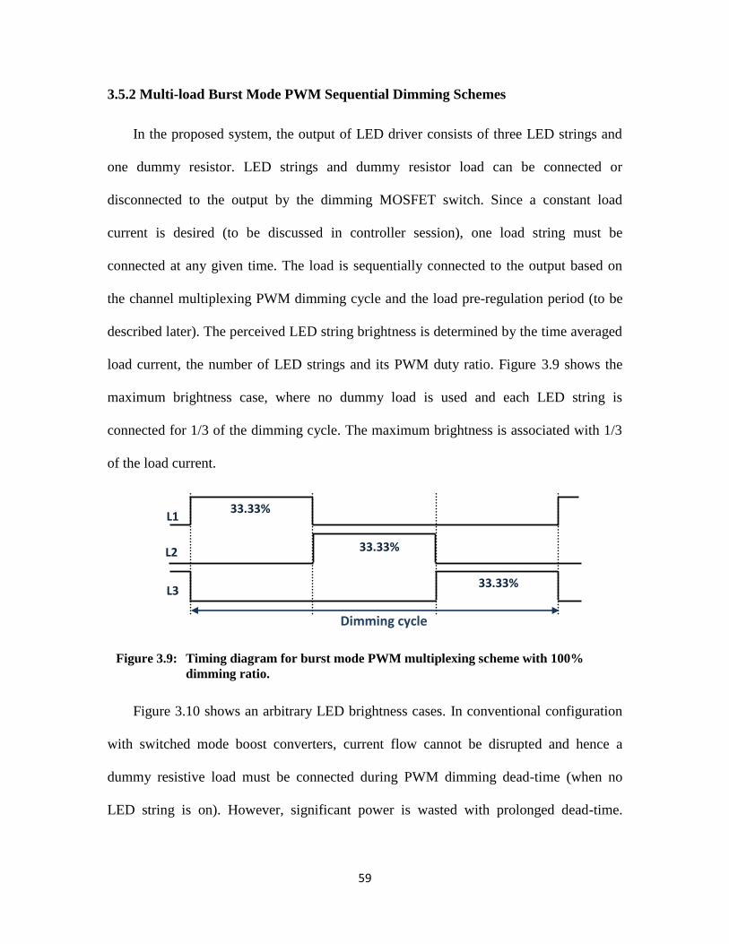
59
3.5.2 Multi-load Burst Mode PWM Sequential Dimming Schemes
In the proposed system, the output of LED driver consists of three LED strings and
one dummy resistor. LED strings and dummy resistor load can be connected or
disconnected to the output by the dimming MOSFET switch. Since a constant load
current is desired (to be discussed in controller session), one load string must be
connected at any given time. The load is sequentially connected to the output based on
the channel multiplexing PWM dimming cycle and the load pre-regulation period (to be
described later). The perceived LED string brightness is determined by the time averaged
load current, the number of LED strings and its PWM duty ratio. Figure 3.9 shows the
maximum brightness case, where no dummy load is used and each LED string is
connected for 1/3 of the dimming cycle. The maximum brightness is associated with 1/3
of the load current.
Figure 3.10 shows an arbitrary LED brightness cases. In conventional configuration
with switched mode boost converters, current flow cannot be disrupted and hence a
dummy resistive load must be connected during PWM dimming dead-time (when no
LED string is on). However, significant power is wasted with prolonged dead-time.
Figure 3.9: Timing diagram for burst mode PWM multiplexing scheme with 100%
dimming ratio.
33.33%
L1
L2
L3
Dimming cycle
33.33%
33.33%

60
Obviously this is not a desired dimming method. Session 3.5.4 will introduce an energy
conservation based, which can effectively solve the problem.
3.5.3 Close Loop current mode PI Controller
Step 1: Control schemes
For the switched mode converters, the output voltage is a function of the input line
voltage Vg(t), duty cycle d(t) and load impedance Zload(t). The output voltage regulation is
achieved through a feed-back loop. Two fundamental control schemes can be used for
close-loop voltage regulation, voltage mode control scheme and current mode control
scheme. For voltage mode control, the output voltage variation can be expressed as a
linear combination of , ,and .
(3.4)
In current mode control, output voltage regulation is achieved through inductor
current regulation. The output voltage can be expressed as
(3.5)
Figure 3.10: Timing diagram for burst mode PWM multiplexing scheme with arbitrary
dimming ratio.
L1
L2
L3
D1
D2
D3
L4 Dload
Dimming cycle
Dimming dead-time

61
In this work, current programmed mode control is used for the following reasons.
First, current mode control has simpler dynamics. This can be observed from their
control-to-output transfer functions. In voltage mode control,
(3.6)
and in current programmed mode,
(3.7)
the second pole is moved to a higher frequency (near switching frequency) and the small-
signal control-to-output transfer function
contains one less pole than
. Therefore the
output voltage control can be obtained without the use of compensator lead network.
Secondly, since the inductor current is directly regulated, excessive current condition and
fault conditions will be effectively avoided.
Step 2: Analog PI controller design
In the PI controller design, it is essential to determine the zero frequency c and
controller grain K as in K(1+s/c). Due to the existence of right half plane zero in Gvc(s),
the controller bandwidth (BW) and phase margin (PM) can be very sensitive to the
variation of circuit parameters such as load current, power line variation (Vg), and circuit
parasitic components. In this work, the effect of power line variation is analyzed. The
compensator is designed at nominal input voltage Vg = 4.5 V, the gain is chosen to be 28,
and this gives PM = 52.3o and BW = 10.6 kHz. However the same compensator fail to
work when Vg = 2.7 V since PM will reduce to -11.1 o
at this supply voltage. This will
cause the system to become unstable. Also, the PM and BW is inversely related to each

62
other, the larger the phase margin the narrower the bandwidth. In order to have a
reasonable large phase margin over the entire operating power line range, the band width
has to be reduced through the reduction of the controller gain K. Table 3.3 shows the PM
and BW at different controller gains for input ranging from 2.7 V to 6 V. We note that
when K = 10, the PM will result in the range of 59.4 o to 72.4
o and bandwidth will be in
the range of 4.7 kHz to 6.16 kHz. The compensator gain has to be designed to be as low
as 10 to accommodate the entire range of the input voltage. Figure 3.11 shows the
control-to-output transfer function bode plot at with Vg = 2.7 V and K = 10.
The narrow control bandwidth means that the recovery will be slow during load
transient. Since the load current is designed to be constant in this work, the low close
loop bandwidth will not degrade the close-loop performance. Therefore, the proposed
LED driver topology can effectively avoid the narrow control bandwidth problem
associated with right half plane zero in the boost converter design.
Table 3.3 The influence of supply line variation on control loop
Vg = 4.5 V Vg = 2.7 V Vg = 6 V
K = 28 PM 52.3
o -11.1
o 62.5
o
BW 10.6 kHz 151 kHz 12.5 kHz
K = 27 PM 53.9
o 8.3
o 63.7
o
BW 9.98 kHz 26.9 kHz 12 kHz
K = 10 PM 72.4
o 59.4
o 76.8
o
BW 4.7 kHz 3.18 kHz 6.16 kHz

63
Step3: Digital PI controller design
The digital PI controller is constructed by Look-Up Tables (LUTs) containing the
coefficients C0 and C1 in the following equation: [19]-[21]
D[n] = D[n1] + C0 × e[n] – C1 × e[n-1] (3.8)
By using pole-zero matching, the digital PI controller is designed from its analog
counterpart. The resulting controller has C0 = 80.0017 and C1= 79.9983.
3.5.4 Energy Conservation Based Close Loop PI Control Scheme
Figure 3.12 shows 4-channel PWM dimming timing diagram for arbitrary dimming
ratios. Figure 3.12(a) is the case with a dummy resistive load during PWM dead-time
Figure 3.11: Bode plot of control-to-output transfer function at Vg = 2.7 V for K = 10.

64
(discussed in 3.5.2). Figure 3.12(b) is the proposed method where the dimming dead-time
is divided into two periods, energy conservation duration and load pre-regulation
duration. In the conservation period, the load is disconnected from the output and
inductor current circulates through the auxiliary switch. During this time, no power is
wasted except for the conduction loss from the auxiliary switch and from the series
resistance of the inductor. The close loop controller is temporarily disabled and the main
switch is turned off. The pre-regulation period is designed to compensate for the inductor
current loss (due to freewheeling path resistive parasitic) and the output charge leaked
during the conservation period, which effectively eliminates brightness flickering and
achieves good dimming accuracy. Since the dummy resistive load is only connected for a
short time before the first LED string (L1) turns on, significant power saving can be
accomplished. Moreover, the power loss associated with the dummy load can be
optimized by adjusting the pre-regulation duration. For example, a shorter pre-regulation
duration gives better efficiency but requires faster close loop control scheme to ensure
constant load current when first LED string turns on. Compared with PWM dynamic bus
voltage regulation [22], the proposed approach no longer requires LED voltage sensing
and reference current adjustment, thus greatly simplifies the LED driver design.

65
3.5.5 LED Selection
An important design consideration is the current associated with the maximum
required brightness, defined as the full current level. The multiplexing of three LED
strings requires a pulsating current equal to three times that of the full current level to
achieve maximum brightness. Figure 3.13 shows the relationship between full current,
pulsating current and maximum rated current in a LED. The pulsating current requires the
LEDs to operate over its rated current to some degree. As long as the average current can
Figure 3.12: Timing diagram for arbitrary dimming duty ratios.
(a) Constant current regulation using dummy resistive load.
(b) Constant current regulation using energy conservation scheme.
L1
L2
L3
D1
D2
D3
L4 Dload
Dimming cycle
Dimming dead-time
Pre-regulation
L4 Dload
swi_aux
swi_main
Daux
Conservation
(a)
(b)
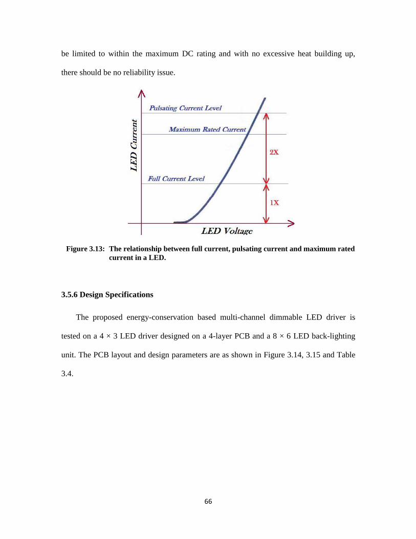
66
be limited to within the maximum DC rating and with no excessive heat building up,
there should be no reliability issue.
3.5.6 Design Specifications
The proposed energy-conservation based multi-channel dimmable LED driver is
tested on a 4 × 3 LED driver designed on a 4-layer PCB and a 8 × 6 LED back-lighting
unit. The PCB layout and design parameters are as shown in Figure 3.14, 3.15 and Table
3.4.
Figure 3.13: The relationship between full current, pulsating current and maximum rated
current in a LED.

67
Figure 3.14: The 4-layer PCB layout of the proposed 4 × 3 LED driver.
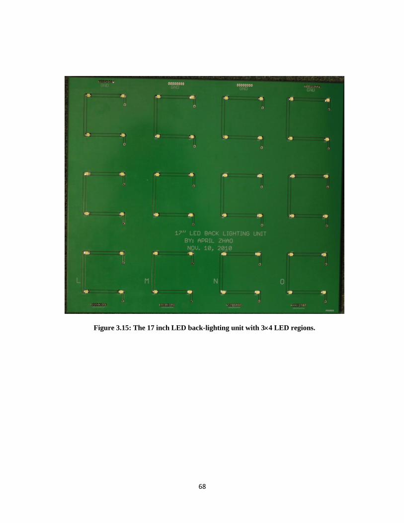
68
Figure 3.15: The 17 inch LED back-lighting unit with 34 LED regions.

69
Table 3.4 Summary of design parameters for a 4.5 V to 14 V DC-DC boost converter
Components Abbreviation Value Part Number
Output
capacitor Cout 400 µF GRM31CF50J107ZE01L
Inductance L 10 µH IHLP6767
Main
MOSFET Smain IRLML0030
Bypass
MOSFET Saux
IRF7821
PWM dimming
MOSFET Sdim
IRF7821
Main
MOSFET
Gate Driver
GD_main MIC4422
Bypass
MOSFET
Gate Driver
GD_aux
MIC4422
Dimming
Gate Driver GD_dimming
UCC27424
10-bit
ADC ∆ADC 1 mV AD9200
10-bit
DAC ∆DAC 1 mV AD9750
Sense
Resistor Rsen 0.1 Ω KRL32C.100CT
70
3.6 System Verification and Experimental Results
The proposed multi-channel LED driver with local dimming capabilities is verified
experimentally using an FPGA implementation for the digital controller, an LED driver
output stage and a LED back-lighting panel. The digital controller implements channel
current multiplexing scheme, closed-loop voltage regulation for 4-LED drivers, and
serial-to-parallel dimming ratio communication module. The testing is conducted in two
phases. Phase I focuses on the functionality and the efficiency of each one of 4 multi-
channel LED drivers. The proposed energy conservation based high-efficiency dimming
scheme is tested on the 3-channel LED driver regulating one column of 3 strings 4
LEDs. Phase II focuses on the local dimming system integration (this was a task for a 4th
year design project group). Since this thesis focuses on efficiency enhancement
techniques, only the phase I testing procedure and results are discussed. The phase I
testing is designed in two steps. First, for certain LED dimming ratio, the load current on
each LED string is measured during PWM dimming switching transient. Second the
conversion efficiency is measured for dimming ratio varying from 10% to 100%. Testing
condition is summarized in Table 3.5.
Table 3.5: Testing Conditions of the 4.5 V to 14 V 180 mA 3-channel LED driver
Parameter Value
Switching frequency 781 kHz
Input voltage 4.5 V
Output voltage 14 V
Output current 180 mA
PWM dimming frequency 200 Hz
Pre-regulation duration 1/8 (0.625 ms), 1/16 (0.3125 ms)

71
3.6.1 Multi-channel Load Switching Transient Test
The load switching transient is tested for three channels LED with dimming ratios of
20%, 40% and 60% and a pre-regulation period equal to 1/8 dimming cycle. The load
current waveform during the energy conservation and pre-regulation periods is as shown
in Figure 3.16. As can be seen, the load current drops to zero during the energy
conservation period. We note that current ringing only occurs at the beginning of the pre-
regulation period due to the regulation of close-loop controller. The load current remains
constant during the duration of the three LED channels PWM dimming cycle.
Figure 3.16: Load current waveform during PWM dimming period, energy conservation
and pre-regulation period.

72
3.6.2 Multi-channel LED Driver Efficiency Test
The proposed PWM dimming scheme was verified experimentally with 2 pre-
regulation time (1/8 and 1/16 of dimming cycle, corresponding to 0.625 ms and 0.3125
ms), the conversion efficiency is measured for dimming ratio between 10 to 100 %. An
overall efficiency of 50 to 90 % was achieved over a wide range of LED luminance. As
shown in Figure 3.17, there is a substantial improvement if dummy load resistor is used.
This efficiency level also compares favourably with previously published result [17].
Also, the case with pre-regulation time equal to 1/16 of the dimming cycle gives better
efficiency.
0%
20%
40%
60%
80%
100%
0% 20% 40% 60% 80% 100%
LED
Dri
ver
Effi
cien
cy
Brightness Ratio
Dpre_reg = 1/16
Dpre_reg = 1/8
with dummy load
Figure 3.17: Measured LED driver efficiency measurements for pre-regulation times
equal to1/16, 1/8 of PWM dimming period.

73
3.7 Summary
This chapter discussed the implantation and verification of the proposed energy
conservation based high efficiency dimmable multi-channel LED driver. An overall
efficiency of 50 to 90 % was obtained over a wide range of LED luminance. The proposed
approach completely eliminates the dedicated linear current regulator and sensing components in
each LED channel as required by recently reported methods. This work is well suited for digital
IC implementation for dynamic LED luminance adjustment.

74
CHAPTER 4
Conclusions
In modern electronic systems, power management circuits play a very important role
for the enhancement of the overall system efficiency. In this thesis two efficiency
optimization techniques for switched mode power supplies were described.
The first technique is a dead-time optimization technique used to improve the power
conversion efficiency during stead-state operation and under frequent load transients. The
proposed method can detect and measure the unwanted body-diode conduction and
optimize the dead-time on the fly [23]. In addition to the elimination of the body-diode
conduction loss, the reverse recovery loss is completely avoided since the body-diode
never becomes fully turned on. This method successfully circumvents the drawbacks of
many existing dead-time control schemes. It constantly optimizes the dead-time during
any load condition such that the maximum possible conversion efficiency is always
ensured..
The second technique is an energy conservation technique that allows the free-
wheeling of inductor current during no-load conditions to improve the efficiency [24].
Multi-channel load current sharing is also introduced to simplify the regulation in the
voltage control loop. These techniques were implemented and verified in a 4 3 LED
driver unit. The proposed dimming method completely eliminates the need for a
75
dedicated linear regulator and various sensing components in each LED strings. It offers
a high efficiency dimming solution and is very well suited for multi-string LED dynamic
luminance adjustment.
Research in high efficiency power management circuit is an on-going process. In
relation to this thesis, two topics require further exploration. One is the performance of
the proposed one-step dead-time optimization algorithm under different close-loop
control schemes. Second, the choice of pre-regulation time can be investigated such that
further optimization of the efficiency under various dimming requirements can be
achieved.
76
References
[1] R. W. Erickson and D. Maksimovic, “Fundamentals of Power Electronics,” 2nd
edition.
[2] Designing fast response synchronous buck regulators using the TPS5210” APPL.
Rep., SLVA044, Texas Instruments, 1999.
[3] A. Stratakos, S. Sanders, and R. Brodersen, “A low-voltage CMOS DC-DC
converter for a portable battery-operated system,” in IEEE Power Electronics
Specialists Conference, 1993 Rec., vol. 1, pp. 619-626, June 1994.
[4] S. Mapus, “Predictive gate drive boosts synchronous DC/DC power converter
efficiency,” APPL. Rep. SLUA281, Texas Instruments, Apr. 2003.
[5] O. Trescases, W.T. Ng, and S. Chen, “Precision gate drive timing in a zero-voltage
switching DC-DC converter,” in Proc. IEEE Int. Symp. Power Semicond. Devices
ICs, 2004, pp. 55-58.
[6] B. Acker, C.R. Sullivan, and S.R. Sanders, “Synchronous rectification with
adaptive timing control,” in IEEE Power Electronics Specialists Conference, 1995,
pp. 88-95.
[7] V. Yousefzadeh, and D. Maksimovic, “Sensorless optimization of dead-times in
DC-DC converters with synchronous rectifiers,” IEEE Transactions on Power
Electronics, vol. 21, no.4, July 2006.
[8] E.O. Malley, K. Rinne, “A programmable digital pulse width modulator providing
versatile pulse patterns and supporting switching frequencies beyond 15 MHz,” in
IEEE Applied Power Electronics Conference, 2004, Vol. 1, pp. 53-59, Feb. 2004.
[9] V. Yousefzadeh, T. Takayama, and D. Maksimovic, “Hybrid DPWM with Digital
Delay-Locked Loop,” in IEEE COMPEL Workshop, July 2006.
77
[10] R. Miftakhutdinov “Synchronous buck regulator design using the TI TPS5311 high-
frequency hysterectic controller,” Analog Applications Journal, Texas Instruments,
Nov. 1999.
[11] “LED backlight,” White Paper, Visual Display Division, Digital Media Network
Business, Jul. 2006.
[12] L. Yao, “LED BLU and green high tech life,” CMO LED Day Forum,
DisplaySearch Taiwan, 2008.
[13] H.J. Hahm, “LED BLU overview and requirements”, Samsung Electro - Mechanics
[14] Y. Hu and M. M. Jovanovic, “LED driver with self-adaptive drive voltage,” IEEE
Trans. Power Electron., vol. 23, no. 6. pp. 3116-3125, Nov. 2008.
[15] L. Burgyan and F. Prinz, “High efficiency LED driver,” U.S. Patent 6690146, Feb.
10, 2004.
[16] K. I. Huw and Y. T. Yau, “Applying one-comparator counter-based sampling to
current sharing control of multi-channel LED strings,” in Proc. IEEE Appl. Power
Electron. Conf. (APEC), Feb. 2010, pp. 737-742.
[17] D. Gacio, J. M. Alonso, J. Garcia, L. Campa, M. Crespo and M. Rico-Secades,
“High frequency PWM dimming technique for high power factor converters in LED
lighting,” in Proc. IEEE Appl. Power Electron. Conf. (APEC), Feb. 2010, pp. 743-
749.
[18] S. Sarhan and C. Richardson, “A matter of light,” in Power Management DesignLine,
National Semiconductor. May 2008.
[19] L.P. Guo, “Implementation of digital PID controllers for DC-DC converters using
digital signal processors,” in Proc. IEEE Electronic Information Technology Conf.
(EIT), 2007, pp. 306-311.

78
[20] V. Subasri, K. Lavanya and B. Umamaheswari, “Implementation of digital PID
controller in field programmable gate array (FPGA)”, in Proc. India International
Conference on Power Electronics, 2006, pp. 172-176.
[21] A. Prodic and D. Maksimovic, “Design of a digital PID regulator based on look-up
tables for control of high-frequency DC-DC converters”, in Proc. Computers in
Power Electronics Workshop, 2002, pp. 18-22.
[22] M. Doshi and R. Zane, “Digital architecture for driving large LED arrays with
dynamic bus voltage regulation and phase shifted PWM,” in Proc. IEEE Appl.
Power Electron. Conf. (APEC), Feb. 2007, pp. 287 - 293.
[23] A. Zhao, A.A. Fomani and W.T. Ng, “One-step digital dead-time correction for
DC-DC converters,” in Proc. Applied Power Electronics Conf. (APEC), Feb. 2010,
pp. 132-137.
[24] A. Zhao and W. T. Ng, “An energy conservation based high-efficiency dimmable
multi-channel LED driver” submitted to Energy Conversion Congress & Exposition
2011 (ECCE).