EEL 4783: HDL in Digital System Design - eecs.ucf.edueecs.ucf.edu/~mingjie/EEL4783/lect.11.pdf ·...
76
1 EEL 4783: HDL in Digital System Design Lecture 11: Revisiting Sequential Circuits Prof. Mingjie Lin
Transcript of EEL 4783: HDL in Digital System Design - eecs.ucf.edueecs.ucf.edu/~mingjie/EEL4783/lect.11.pdf ·...

1
EEL 4783: HDL in Digital System Design
Lecture 11: Revisiting Sequential Circuits
Prof. Mingjie Lin

2
Sequential Basics
Sequential circuits Outputs depend on current inputs and previous inputs Store state: an abstraction of the history of inputs
Usually governed by a periodic clock signal

3
D-Flipflops
1-bit storage element We will treat it as a basic component
Other kinds of flipflops SR (set/reset), JK, T (toggle)
D Q
clkD
clk
Q

4
Registers
Store a multi-bit encoded value One D-flipflop per bit Stores a new value on
each clock cycle
wire [n:0] d;reg [n:0] q;
...
always @(posedge clk)
q <= d;
event list
nonblocking
asignment
D Q
clk
D Q
clk
D Q
clk
d(0)
d(1)
d(n)
n n
q(0)
q(1)
q(n)clk
D Q
clk

5
Pipelines Using Registers
Total delay = Delay1 + Delay2 + Delay3
Interval between outputs > Total delay
Clock period = max(Delay1, Delay2, Delay3)
Total delay = 3 × clock period
Interval between outputs = 1 clock period
D Q
clk
combin-ational
circuit 1
D Q
clk
combin-ational
circuit 2
D Q
clk
combin-ational
circuit 3
d_in
clk
d_out
combin-ational
circuit 1
combin-ational
circuit 2
combin-ational
circuit 3d_in

6
Registers
Store a multi-bit encoded value One D-flipflop per bit Stores a new value on
each clock cycle
wire [n:0] d;reg [n:0] q;
...
always @(posedge clk)
q <= d;
event list
nonblocking
asignment
D Q
clk
D Q
clk
D Q
clk
d(0)
d(1)
d(n)
n n
q(0)
q(1)
q(n)clk
D Q
clk

7
Pipeline Example
Compute the average of corresponding numbers in three input streams
New values arrive on each clock edge
module average_pipeline ( output reg signed [5:-8] avg, input signed [5:-8] a, b, c, input clk );
wire signed [5:-8] a_plus_b, sum, sum_div_3; reg signed [5:-8] saved_a_plus_b, saved_c, saved_sum; ...

8
Pipeline Example
...
assign a_plus_b = a + b;
always @(posedge clk) begin // Pipeline register 1 saved_a_plus_b <= a_plus_b; saved_c <= c; end
assign sum = saved_a_plus_b + saved_c;
always @(posedge clk) // Pipeline register 2 saved_sum <= sum;
assign sum_div_3 = saved_sum * 14'b00000001010101;
always @(posedge clk) // Pipeline register 3 avg <= sum_div_3;
endmodule

9
D-Flipflop with Enable
Storage controlled by a clock-enable stores only when CE = 1 on a rising edge of the clock
CE is a synchronous control input
DCE
Q
clk D
CE
clk
Q

10
Register with Enable
One flipflop per bit clk and CE wired in common
wire [n:0] d;wire ce;reg [n:0] q;...
always @(posedge clk)
if (ce) q <= d;

11
Register with Synchronous Reset
Reset input forces stored value to 0 reset input must be stable around rising edge of clk
always @(posedge clk)
if (reset) q <= 0;
else if (ce) q <= d;
DCE
Q
clkreset
D
CE
reset
clk
Q
1 2 3 4 5 6 7 8

12
Register with Asynchronous Reset
Reset input forces stored value to 0 reset can become 1 at any time, and effect is immediate reset should return to 0 synchronously
DCE
Q
clkreset
D
CE
reset
clk
Q
1 2 3 4 5 6 7 8

13
Asynch Reset in Verilog
always @(posedge clk or posedge reset)
if (reset) q <= 0;
else if (ce) q <= d;
reset is an asynchronous control input here
include it in the event list so that the process responds to changes immediately

14
Example: Accumulator
Sum a sequence of signed numbers A new number arrives when data_en = 1 Clear sum to 0 on synch reset
module accumulator ( output reg signed [7:-12] data_out, input signed [3:-12] data_in, input data_en, clk, reset );
wire signed [7:-12] new_sum;
assign new_sum = data_out + data_in;
always @(posedge clk) if (reset) data_out <= 20'b0; else if (data_en) data_out <= new_sum;
endmodule

15
Flipflop and Register Variations
module flip_flop_n ( output reg Q, output Q_n, input pre_n, clr_n, D, input clk_n, CE );
always @( negedge clk_n or negedge pre_n or negedge clr_n ) begin if ( !pre_n && !clr_n) $display("Illegal inputs: pre_n and clr_n both 0"); if (!pre_n) Q <= 1'b1; else if (!clr_n) Q <= 1'b0; else if (CE) Q <= D; end
assign Q_n = ~Q;
endmodule
DCE
Q
Qclk
pre
clr

16
Shift Registers
Performs shift operation on stored data Arithmetic scaling Serial transfer
of data
DD_in
CEload_en
Q
clk
D
CE
Q
clk
0
1
D
CE
Q
clk
0
1
D
CE
Q
clk
0
1
Q(n–1)
Q(n–2)
Q(0)
D(n–1)
D(n–2)
D(0)
clkCE
load_en

17
Example: Sequential Multiplier
16×16 multiply over 16 clock cycles, using one adder Shift register for multiplier bits Shift register for lsb’s of accumulated product
17-bit reg
resetCE
D Q
clk
D
16-bit reg
CE
Q
clk
D_in
15-bitshift reg
CE
Q
clk
16-bitshift regD_inD
CEload_en
Q
clk x
16-bitadder
c0
y
c16
s15...0
16 15
031...16
P(14...0)
P(31...15)
y(15...0)
x(15...0)
y_load_eny_ce
x_ce
P_resetP_ce
clk

18
Latches
Level-sensitive storage Data transmitted while enable is '1'
transparent latch
Data stored while enable is '0'
D Q
LED
LE
Q

19
Feedback Latches
Feedback in gate circuits produces latching behavior Example: reset/set (RS) latch
S
R
Q
Current RTL synthesis tools don’t accept Verilog models with unclocked feedback
+V
Q
Q
R
S

20
Latches in Verilog
Latching behavior is usually an error!
always @* if (~sel) begin z1 <= a1; z2 <= b1; end else begin z1 <= a2; z3 <= b2; end
Oops!Should bez2 <= ...
Values must be stored for z2 while sel = 1 for z3 while sel = 0

21
Counters
Stores an unsigned integer value increments or decrements the value
Used to count occurrences of events repetitions of a processing step
Used as timers count elapsed time intervals by incrementing periodically

22
Free-Running Counter
Increments every rising edge of clk up to 2n–1, then wraps back to 0 i.e., counts modulo 2n
This counter is synchronous all outputs governed by clock edge
D Q
clk
+1 Q
clk

23
Example: Periodic Control Signal
Count modulo 16 clock cycles Control output = 1 every 8th and 12th cycle decode count values 0111 and 1011
+1
clk
ctrl
0
1
2
3
0
1
2
3
D Q
clk
D Q
clk
D Q
clk
D Q
clk

24
Example: Periodic Control Signal
module decoded_counter ( output ctrl, input clk );
reg [3:0] count_value;
always @(posedge clk) count_value <= count_value + 1;
assign ctrl = count_value == 4'b0111 || count_value == 4'b1011;
endmodule

25
Count Enable and Reset
Use a register with control inputs
Increments when CE = 1 on rising clock edge
Reset: synch or asynch
+1Q
clk
CEreset
clk
D
CE
Q
reset

26
Terminal Count
Status signal indicating final count value
TC is 1 for one cycle in every 2n cycles
frequency = clock frequency / 2n
Called a clock divider
counter
Q0Q1
Qnclk
TC

27
Divider Example
Alarm clock beep: 500Hz from 1MHz clock
counttone2
tone
clk
10-bitcounter
Q
TCclk
D
CE
Q
clk
tone
tone2
count
clk
1 100 2 2 10 2 10
1023 1023 1023

28
Divide by k
Decode k–1 as terminal count and reset counter register
Counter increments modulo k
Example: decade counter Terminal count = 9
clk Q0Q1Q2Q3
Q0Q1Q2Q3
clk
reset
counter

29
Decade Counter in Verilog
module decade_counter ( output reg [3:0] q, input clk );
always @(posedge clk) q <= q == 9 ? 0 : q + 1;
endmodule

30
Down Counter with Load
Load a starting value, then decrement Terminal count = 0
Useful for interval timer
D Q
clk
–1
=0?
Q
TC
clkload
D
0
1

31
Loadable Counter in Verilog
module interval_timer_rtl ( output tc, input [9:0] data, input load, clk );
reg [9:0] count_value;
always @(posedge clk) if (load) count_value <= data; else count_value <= count_value - 1;
assign tc = count_value == 0;
endmodule

32
Reloading Counter in Verilog
module interval_timer_repetitive ( output tc, input [9:0] data, input load, clk );
reg [9:0] load_value, count_value;
always @(posedge clk) if (load) begin load_value <= data; count_value <= data; end else if (count_value == 0) count_value <= load_value; else count_value <= count_value - 1;
assign tc = count_value == 0;
endmodule

33
Ripple Counter
Each bit toggles between 0 and 1 when previous bit changes from 1 to 0D
Q
Q
clk
D
Q
Q
clk
D
Q
Q
clk
D
Q
Q
clk
Q0
Q1
Q2
Qn
clk
Q1
Q0
Q0
clk
Q1
Q2
Q2

34
Ripple or Synch Counter?
Ripple counter is ok if length is short clock period long relative to flipflop delay transient wrong values can be tolerated area must be minimal
E.g., alarm clock Otherwise use a synchronous counter

35
Datapaths and Control
Digital systems perform sequences of operations on encoded data
Datapath Combinational circuits for operations Registers for storing intermediate results
Control section: control sequencing Generates control signals
Selecting operations to perform Enabling registers at the right times
Uses status signals from datapath

36
Example: Complex Multiplier
Cartesian form, fixed-point operands: 4 pre-, 12 post-binary-point bits result: 8 pre-, 24 post-binary-point bits
Subject to tight area constraints
a=a r+jai b=br +jbi
p=ab=pr+jpi=(arbr−aib i)+j (arb i+aibr )
4 multiplies, 1 add, 1 subtract Perform sequentially using 1
multiplier, 1 adder/subtracter

37
Complex Multiplier Datapath
0
1
0
1
D
CE
Q
clk
D
CE
Q
clk
× ±
D
CE
Q
clk
D
CE
Q
clk
p_r
p_i
a_r
a_i
b_r
b_i
a_sel
b_selpp1_cepp2_ce
subp_r_cep_i_ce
clk

38
Complex Multiplier in Verilog
module multiplier ( output reg signed [7:-24] p_r, p_i, input signed [3:-12] a_r, a_i, b_r, b_i, input clk, reset, input_rdy );
reg a_sel, b_sel, pp1_ce, pp2_ce, sub, p_r_ce, p_i_ce;
wire signed [3:-12] a_operand, b_operand; wire signed [7:-24] pp, sum reg signed [7:-24] pp1, pp2;
...

39
Complex Multiplier in Verilog
assign a_operand = ~a_sel ? a_r : a_i; assign b_operand = ~b_sel ? b_r : b_i;
assign pp = {{4{a_operand[3]}}, a_operand, 12'b0} * {{4{b_operand[3]}}, b_operand, 12'b0};
always @(posedge clk) // Partial product 1 register if (pp1_ce) pp1 <= pp;
always @(posedge clk) // Partial product 2 register if (pp2_ce) pp2 <= pp;
assign sum = ~sub ? pp1 + pp2 : pp1 - pp2;
always @(posedge clk) // Product real-part register if (p_r_ce) p_r <= sum;
always @(posedge clk) // Product imaginary-part register if (p_i_ce) p_i <= sum;
...
endmodule

40
Complex Multiplier in Verilog
assign a_operand = ~a_sel ? a_r : a_i; assign b_operand = ~b_sel ? b_r : b_i;
assign pp = {{4{a_operand[3]}}, a_operand, 12'b0} * {{4{b_operand[3]}}, b_operand, 12'b0};
always @(posedge clk) // Partial product 1 register if (pp1_ce) pp1 <= pp;
always @(posedge clk) // Partial product 2 register if (pp2_ce) pp2 <= pp;
assign sum = ~sub ? pp1 + pp2 : pp1 - pp2;
always @(posedge clk) // Product real-part register if (p_r_ce) p_r <= sum;
always @(posedge clk) // Product imaginary-part register if (p_i_ce) p_i <= sum;
...
endmodule

41
Multiplier Control Sequence
Avoid resource conflict First attempt
1. a_r * b_r → pp1_reg
2. a_i * b_i → pp2_reg
3. pp1 – pp2 → p_r_reg
4. a_r * b_i → pp1_reg
5. a_i * b_r → pp2_reg
6. pp1 + pp2 → p_i_reg Takes 6 clock cycles

42
Multiplier Control Sequence
Merge steps where no resource conflict Revised attempt
1. a_r * b_r → pp1_reg
2. a_i * b_i → pp2_reg
3. pp1 – pp2 → p_r_rega_r * b_i → pp1_reg
4. a_i * b_r → pp2_reg
5. pp1 + pp2 → p_i_reg
Takes 5 clock cycles

43
Multiplier Control Signals
Step a_sel b_sel pp1_ce
pp2_ce sub p_r_ce p_i_ce
1 0 0 1 0 – 0 0
2 1 1 0 1 – 0 0
3 0 1 1 0 1 1 0
4 1 0 0 1 – 0 0
5 – – 0 0 0 0 1
44
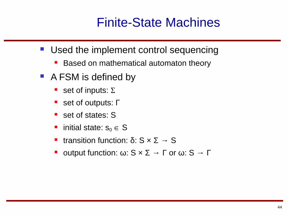
Finite-State Machines
Used the implement control sequencing Based on mathematical automaton theory
A FSM is defined by set of inputs: Σ set of outputs: Γ set of states: S initial state: s0 S transition function: δ: S × Σ → S output function: ω: S × Σ → Γ or ω: S → Γ

45
FSM in Hardware
Mealy FSM: ω: S × Σ → Γ Moore FSM: ω: S → Γ
Mealy FSM only
D
reset
Q
clk
current_state
outputsinputs
clk
reset
nextstatelogic
outputlogic

46
FSM Example: Multiplier Control
One state per step Separate idle state?
Wait for input_rdy = 1 Then proceed to steps 1, 2, ... But this wastes a cycle!
Use step 1 as idle state Repeat step 1 if input_rdy ≠ 1 Proceed to step 2 otherwise
Output function Defined by table on slide 43 Moore or Mealy?
current_state
input_rdy
next_state
step1 0 step1
step1 1 step2
step2 – step3
step3 – step4
step4 – step5
step5 – step1
Transition function

47
State Encoding
Encoded in binary N states: use at least log2N bits
Encoded value used in circuits for transition and output function encoding affects circuit complexity
Optimal encoding is hard to find CAD tools can do this well
One-hot works well in FPGAs Often use 000...0 for idle state
reset state register to idle

48
FSMs in Verilog
Use parameters for state values Synthesis tool can choose an alternative encoding
parameter [2:0] step1 = 3'b000, step2 = 3'b001, step3 = 3'b010, step4 = 3'b011, step5 = 3'b100;
reg [2:0] current_state, next_state ;
...

49
Multiplier Control in Verilog
always @(posedge clk or posedge reset) // State register if (reset) current_state <= step1; else current_state <= next_state;
always @* // Next-state logic case (current_state) step1: if (!input_rdy) next_state = step1; else next_state = step2; step2: next_state = step3; step3: next_state = step4; step4: next_state = step5; step5: next_state = step1; endcase

50
Multiplier Control in Verilog
always @* begin // Output_logic a_sel = 1'b0; b_sel = 1'b0; pp1_ce = 1'b0; pp2_ce = 1'b0; sub = 1'b0; p_r_ce = 1'b0; p_i_ce = 1'b0; case (current_state) step1: begin pp1_ce = 1'b1; end step2: begin a_sel = 1'b1; b_sel = 1'b1; pp2_ce = 1'b1; end step3: begin b_sel = 1'b1; pp1_ce = 1'b1; sub = 1'b1; p_r_ce = 1'b1; end step4: begin a_sel = 1'b1; pp2_ce = 1'b1; end step5: begin p_i_ce = 1'b1; end endcase end

51
State Transition Diagrams
Bubbles to represent states Arcs to represent transitions
Example S = {s1, s2, s3} Inputs (a1, a2):
Σ = {(0,0), (0,1), (1,0), (1,1)}
δ defined by diagram
s1 s2
s3
0, 0
0, 0
0, 1
1, 0
0, 1
1, 0
1, 1
1, 1

52
State Transition Diagrams
Annotate diagram to define output function Annotate states for
Moore-style outputs Annotate arcs for
Mealy-style outputs
Example x1, x2: Moore-style y1, y2, y3: Mealy-style
s1 s2
s3
0, 0 / 0, 0, 01, 0 0, 0
0, 1
0, 0 / 0, 0, 0
0, 1 / 0, 1, 1
/ 0, 1, 1
1, 0 / 1, 0, 0
0, 1 / 0, 1, 1
1, 0 / 1, 0, 0
1, 1 / 1, 1, 1
1, 1 / 1, 1, 1

53
Multiplier Control Diagram
Input: input_rdy Outputs
a_sel, b_sel, pp1_ce, pp2_ce, sub, p_r_ce, p_i_ce
step10, 0, 1, 0, –, 0, 0
01 step2
1, 1, 0, 1, –, 0, 0
step41, 0, 0, 1, –, 0, 0
step5–, –, 0, 0, 0, 0, 1
step30, 1, 1, 0, 1, 1, 0

54
Bubble Diagrams or Verilog?
Many CAD tools provide editors for bubble diagrams Automatically generate Verilog for simulation and synthesis
Diagrams are visually appealing but can become unwieldy for complex FSMs
Your choice... or your manager's!

55
Register Transfer Level
RTL — a level of abstraction data stored in registers transferred via circuits that operate on data
control section
outputsinputs

56
Clocked Synchronous Timing
Registers driven by a common clock Combinational circuits operate during clock cycles (between
rising clock edges)
tco + tpd + tsu < tc
Q1 D2tpdt
cotsu
Q1
clk
D2
tco
tc
tpd
tsu
t

57
Control Path Timing
tco + tpd-s + tpd-o + tpd-c + tsu < tc
tco + tpd-s + tpd-ns + tsu < tc
Ignore tpd-s for a Moore FSM
tpd-s
tpd-c
tpd-o
tpd-ns
tco t
su
tsu

58
Timing Constraints
Inequalities must hold for all paths If tco and tsu the same for all paths
Combinational delays make the difference
Critical path The combinational path between registers with the
longest delay Determines minimum clock period for the entire
system
Focus on it to improve performance Reducing delay may make another path critical

59
Interpretation of Constraints
1. Clock period depends on delays System can operate at any frequency up to a maximum OK for systems where high performance is not the main
requirement
2. Delays must fit within a target clock period Optimize critical paths to reduce delays if necessary May require revising RTL organization

60
Clock Skew
Need to ensure clock edges arrive at all registers at the same time
Use CAD tools to insert clock buffers and route clock signal paths
Q1 D2Q1
clk1
clk2
D2
th

61
Off-Chip Connections
Delays going off-chip and inter-chip Input and output pad delays, wire delays
Same timing rules apply Use input and output registers to avoid adding external delay
to critical path
Q1 D2

62
Asynchronous Inputs
External inputs can change at any time Might violate setup/hold time constraints
Can induce metastable state in a flipflop
Unbounded time to recover
May violate setup/hold time of subsequent flipflop
MTBF=e
k2 t
k1 f f f 2
k 2 >>0
0 1 0 1

63
Synchronizers
If input changes outside setup/hold window Change is simply delayed by one cycle
If input changes during setup/hold window First flipflop has a whole cycle to resolve
metastability
See data sheets for metastability parameters
D Q
clk
D Q
clk
clk
asynch_insynch_in
64
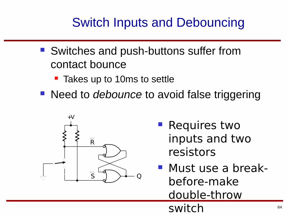
Switch Inputs and Debouncing
Switches and push-buttons suffer from contact bounce Takes up to 10ms to settle
Need to debounce to avoid false triggering
Requires two inputs and two resistors
Must use a break-before-make double-throw switch
Q
R
S
+V

65
Switch Inputs and Debouncing
Alternative Use a single-throw switch Sample input at intervals longer than bounce time Look for two successive samples with the same
value
Assumption Extra circuitry inside the
chip is cheaper than extra components and connections outside
+V

66
Debouncing in Verilog
module debouncer ( output reg pb_debounced, input pb, input clk, reset );
reg [18:0] count500000; // values are in the range 0 to 499999 wire clk_100Hz; reg pb_sampled;
always @(posedge clk or posedge reset) if (reset) count500000 <= 499999; else if (clk_100Hz) count500000 <= 499999; else count500000 <= count500000 - 1;
assign clk_100Hz = count500000 == 0;
always @(posedge clk) if (clk_100Hz) begin if (pb == pb_sampled) pb_debounced <= pb; pb_sampled <= pb; end
endmodule

67
Verifying Sequential Circuits
DUV may take multiple and varying number of cycles to produce output
Checker needs to synchronize with test generator ensure DUV outputs occur when expected ensure DUV outputs are correct ensure no spurious outputs occur
Design UnderVerification
(DUV)Apply
Test Cases Checker
Verification Testbench

68
Example: Multiplier Testbench
`timescale 1ns/1ns
module multiplier_testbench;
parameter t_c = 50;
reg clk, reset; reg input_rdy; wire signed [3:-12] a_r, a_i, b_r, b_i; wire signed [7:-24] p_r, p_i;
real real_a_r, real_a_i, real_b_r, real_b_i, real_p_r, real_p_i, err_p_r, err_p_i;
task apply_test ( input real a_r_test, a_i_test, b_r_test, b_i_test ); begin real_a_r = a_r_test; real_a_i = a_i_test; real_b_r = b_r_test; real_b_i = b_i_test; input_rdy = 1'b1; @(negedge clk) input_rdy = 1'b0; repeat (5) @(negedge clk); end endtask

69
Example: Multiplier Testbench
multiplier duv ( .clk(clk), .reset(reset), .input_rdy(input_rdy), .a_r(a_r), .a_i(a_i), .b_r(b_r), .b_i(b_i), .p_r(p_r), .p_i(p_i) );
always begin // Clock generator #(t_c/2) clk = 1'b1; #(t_c/2) clk = 1'b0; end
initial begin // Reset generator reset <= 1'b1; #(2*t_c) reset = 1'b0; end

70
Example: Multiplier Testbench
initial begin // Apply test cases @(negedge reset) @(negedge clk) apply_test(0.0, 0.0, 1.0, 2.0); apply_test(1.0, 1.0, 1.0, 1.0); // further test cases ... $finish; end
assign a_r = $rtoi(real_a_r * 2**12); assign a_i = $rtoi(real_a_i * 2**12); assign b_r = $rtoi(real_b_r * 2**12); assign b_i = $rtoi(real_b_i * 2**12);

71
Example: Multiplier Testbench
always @(posedge clk) // Check outputs if (input_rdy) begin real_p_r = real_a_r * real_b_r - real_a_i * real_b_i; real_p_i = real_a_r * real_b_i + real_a_i * real_b_r; repeat (5) @(negedge clk); err_p_r = $itor(p_r)/2**(-24) - real_p_r; err_p_i = $itor(p_i)/2**(-24) - real_p_i; if (!( -(2.0**(-12)) < err_p_r && err_p_r < 2.0**(-12) && -(2.0**(-12)) < err_p_i && err_p_i < 2.0**(-12) )) $display("Result precision requirement not met"); end
endmodule

72
Asynchronous Timing
Clocked synchronous timing requires global clock distribution with minimal skew path delay between registers < clock period
Hard to achieve in complex multi-GHz systems Globally asynch, local synch (GALS) systems
Divide the systems into local clock domains Inter-domain signals treated as asynch inputs Simplifies clock managements and constraints Delays inter-domain communication
Delay-insensitive asynchronous systems no clock signals

73
Other Clock-Related Issues
Inter-chip clocking Distributing high-speed clocks on PCBs is hard Often use slower off-chip clock, with on-chip clock
a multiple of off-chip clock Synchronize on-chip with phase-locked loop (PLL)
In multi-PCB systems treat off-PCB signals as asynch inputs
Low power design Continuous clocking wastes power Clock gating: turn off clock to idle subsystems

74
Summary
Registers for storing data synchronous and asynchronous control clock enable, reset, preset
Latches: level-sensitive usually unintentional in Verilog
Counters free-running dividers, terminal count, reset, load, up/down

75
Summary
RTL organization of digital systems datapath and control section
Finite-State Machine (FSM) states, inputs, transition/output functions Moore and Mealy FSMs bubble diagrams
Clocked synch timing and constraints critical path and optimization
Asynch inputs, switch debouncing Verification of sequential systems

76
Final issues
• Please fill out the student info sheet before leaving
• Come by my office hours (right after class)
• Any questions or concerns?