EEE310 MICROPROCESSORS CHAPTER 10compe.hku.edu.tr/Dosyalar/EEE310--Mikroislemciler...8051 FAMILY...
66
EEE310 MICROPROCESSORS CHAPTER 10 M. Fatih Tüysüz
-
Upload
truongnhan -
Category
Documents
-
view
250 -
download
4
Transcript of EEE310 MICROPROCESSORS CHAPTER 10compe.hku.edu.tr/Dosyalar/EEE310--Mikroislemciler...8051 FAMILY...
EEE310 MICROPROCESSORS
CHAPTER 10M. Fatih Tüysüz
CHAPTER 10
Contents
� Intel 8051 Microcontroller
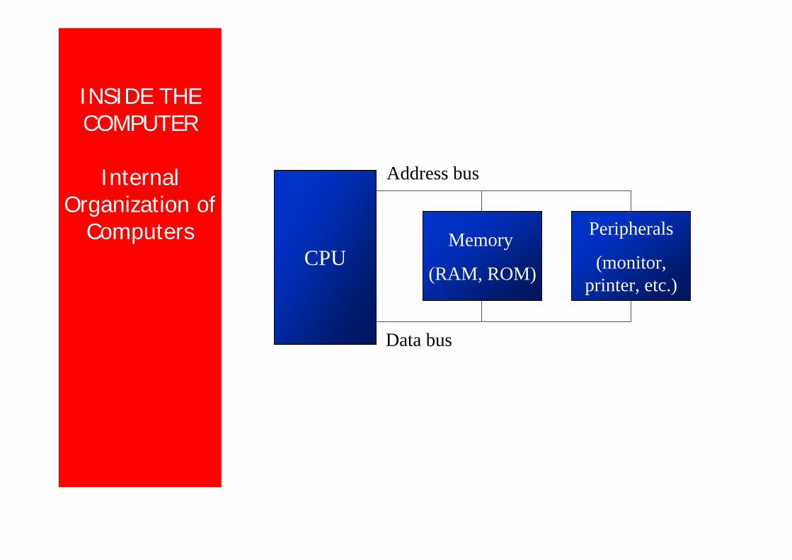
INSIDE THE COMPUTER
Internal Organization of
ComputersCPU
Memory
(RAM, ROM)
Peripherals
(monitor, printer, etc.)
Address bus
Data bus
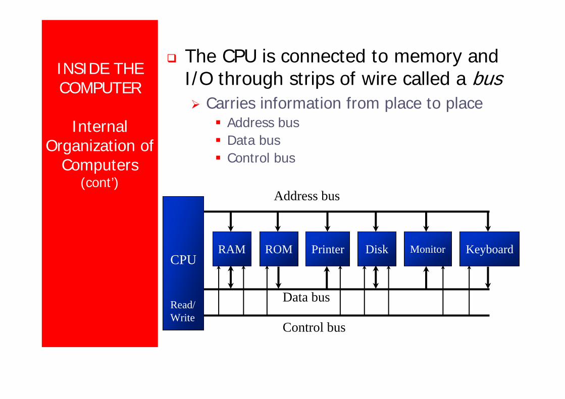
INSIDE THE COMPUTER
Internal Organization of
Computers(cont’)
The CPU is connected to memory andI/O through strips of wire called a bus
Carries information from place to placeAddress busData busControl bus
CPU
Read/Write
RAM
Address bus
Data bus
ROM Printer Disk Monitor Keyboard
Control bus
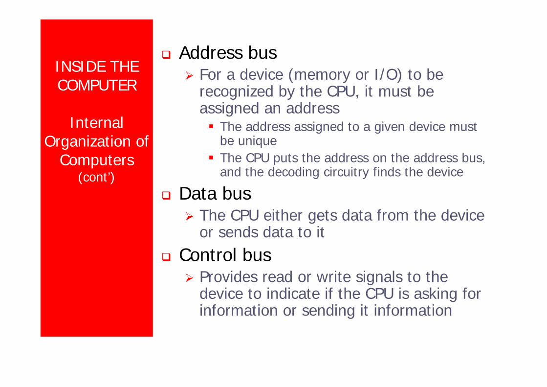
INSIDE THE COMPUTER
Internal Organization of
Computers(cont’)
Address busFor a device (memory or I/O) to berecognized by the CPU, it must beassigned an address
The address assigned to a given device mustbe uniqueThe CPU puts the address on the address bus,and the decoding circuitry finds the device
Data busThe CPU either gets data from the deviceor sends data to it
Control busProvides read or write signals to thedevice to indicate if the CPU is asking forinformation or sending it information

INSIDE THE COMPUTER
More about Data Bus
The more data buses available, thebetter the CPU
Think of data buses as highway lanes
More data buses mean a moreexpensive CPU and computer
The average size of data buses in CPUsvaries between 8 and 64
Data buses are bidirectionalTo receive or send data
The processing power of a computer isrelated to the size of its buses
INSIDE THE COMPUTER
More about Address Bus
The more address buses available, thelarger the number of devices that canbe addressedThe number of locations with which aCPU can communicate is always equalto 2x, where x is the address lines,regardless of the size of the data bus
ex. a CPU with 24 address lines and 16data lines can provide a total of 224 or 16Mbytes of addressable memoryEach location can have a maximum of 1byte of data, since all general-purposeCPUs are byte addressable
The address bus is unidirectional
INSIDE THE COMPUTER
CPU’s Relation to RAM and
ROM
For the CPU to process information,the data must be stored in RAM orROM, which are referred to as primary memoryROM provides information that is fixedand permanent
Tables or initialization programRAM stores information that is notpermanent and can change with time
Various versions of OS and applicationpackagesCPU gets information to be processed
first form RAM (or ROM)if it is not there, then seeks it from a massstorage device, called secondary memory, andtransfers the information to RAM
INSIDE THE COMPUTER
Inside CPUs
RegistersThe CPU uses registers to storeinformation temporarily
Values to be processedAddress of value to be fetched from memory
In general, the more and bigger theregisters, the better the CPU
Registers can be 8-, 16-, 32-, or 64-bitThe disadvantage of more and bigger registersis the increased cost of such a CPU
INSIDE THE COMPUTER
Inside CPUs(cont’)
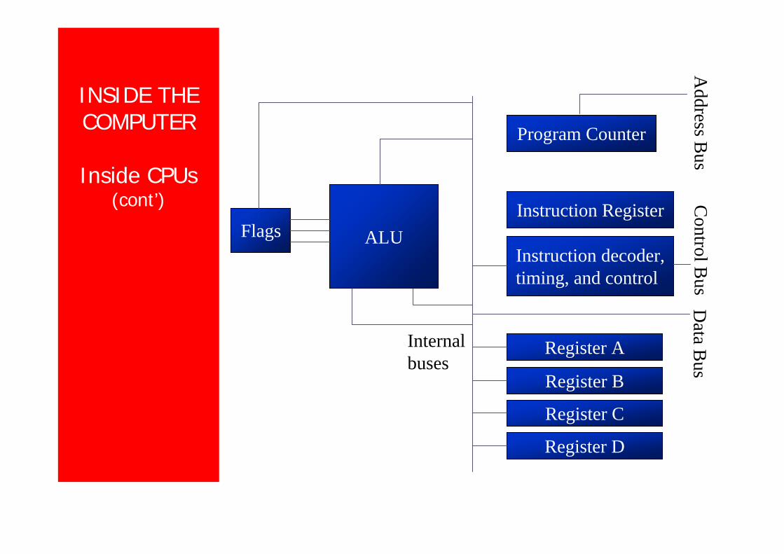
Flags ALU
Program Counter
Instruction Register
Instruction decoder, timing, and control
Register A
Register B
Register C
Register D
Address B
usC
ontrol Bus
Data B
us
Internal buses
INSIDE THE COMPUTER
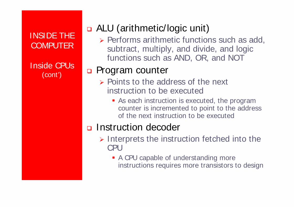
Inside CPUs(cont’)
ALU (arithmetic/logic unit)Performs arithmetic functions such as add,subtract, multiply, and divide, and logicfunctions such as AND, OR, and NOT
Program counterPoints to the address of the nextinstruction to be executed
As each instruction is executed, the programcounter is incremented to point to the addressof the next instruction to be executed
Instruction decoderInterprets the instruction fetched into theCPU
A CPU capable of understanding moreinstructions requires more transistors to design
INSIDE THE COMPUTER
Internal Working of Computers
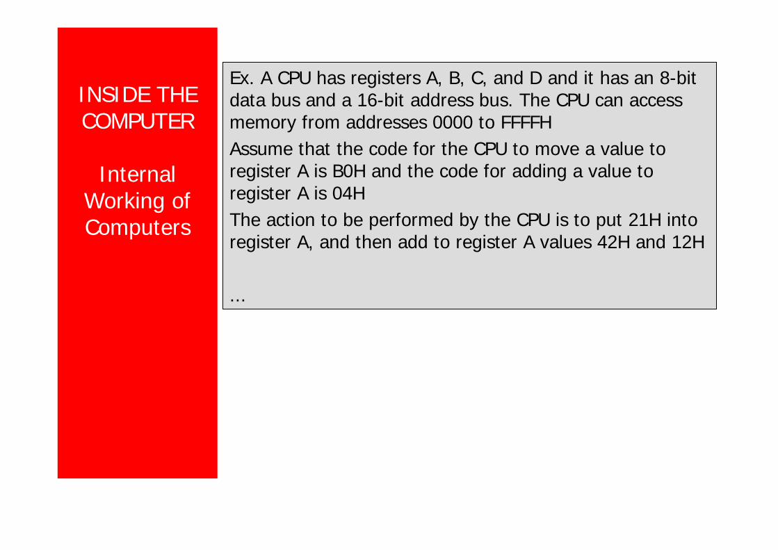
Ex. A CPU has registers A, B, C, and D and it has an 8-bit data bus and a 16-bit address bus. The CPU can access memory from addresses 0000 to FFFFH Assume that the code for the CPU to move a value to register A is B0H and the code for adding a value to register A is 04HThe action to be performed by the CPU is to put 21H into register A, and then add to register A values 42H and 12H
...
INSIDE THE COMPUTER
Internal Working of Computers
(cont’)
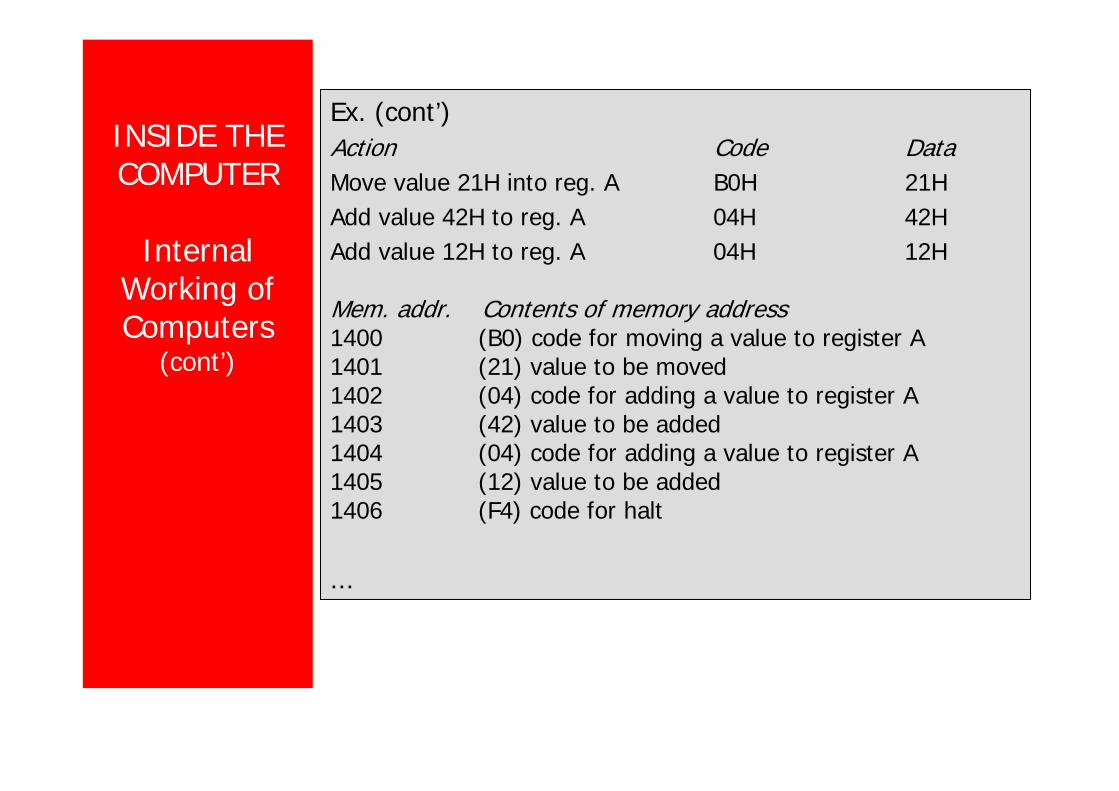
Ex. (cont’)Action Code DataMove value 21H into reg. A B0H 21HAdd value 42H to reg. A 04H 42HAdd value 12H to reg. A 04H 12H
Mem. addr. Contents of memory address1400 (B0) code for moving a value to register A1401 (21) value to be moved1402 (04) code for adding a value to register A1403 (42) value to be added1404 (04) code for adding a value to register A1405 (12) value to be added1406 (F4) code for halt
...
INSIDE THE COMPUTER
Internal Working of Computers
(cont’)
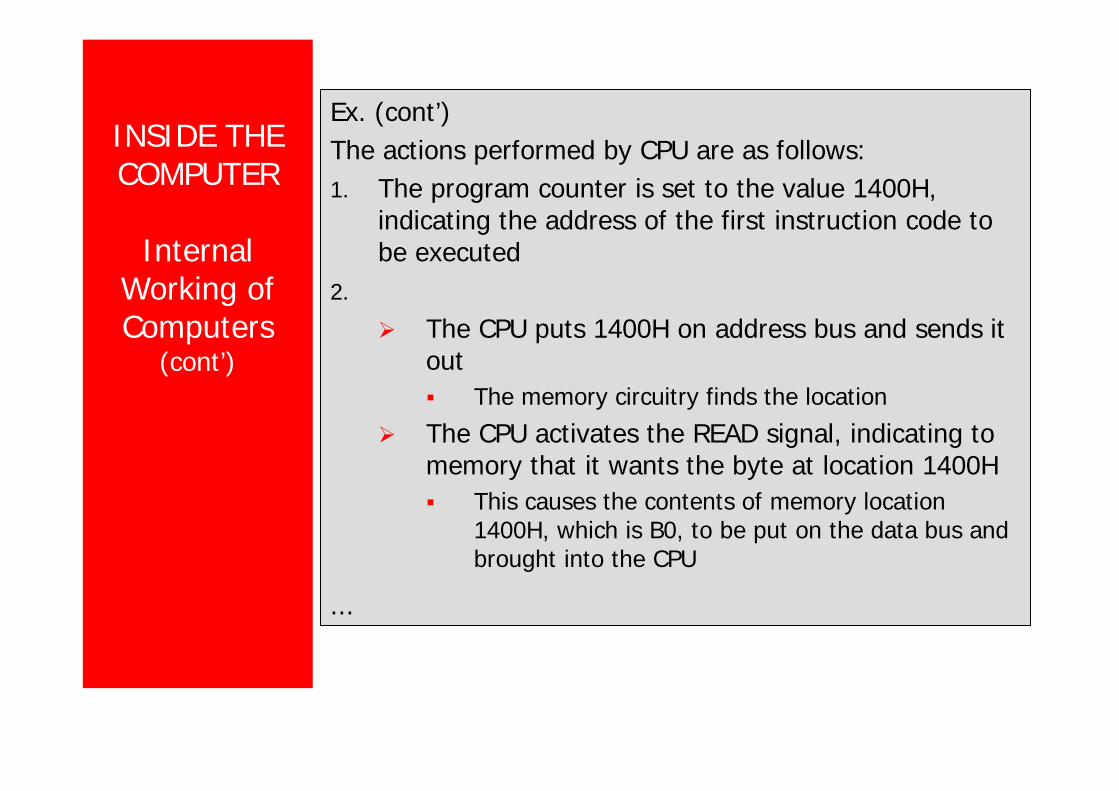
Ex. (cont’)The actions performed by CPU are as follows:1. The program counter is set to the value 1400H,
indicating the address of the first instruction code tobe executed
2.
The CPU puts 1400H on address bus and sends itout
The memory circuitry finds the location
The CPU activates the READ signal, indicating tomemory that it wants the byte at location 1400H
This causes the contents of memory location1400H, which is B0, to be put on the data bus andbrought into the CPU
...
INSIDE THE COMPUTER
Internal Working of Computers
(cont’)
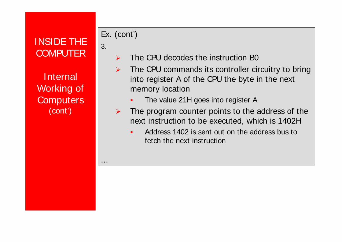
Ex. (cont’)3.
The CPU decodes the instruction B0The CPU commands its controller circuitry to bringinto register A of the CPU the byte in the nextmemory location
The value 21H goes into register A
The program counter points to the address of thenext instruction to be executed, which is 1402H
Address 1402 is sent out on the address bus tofetch the next instruction
...
INSIDE THE COMPUTER
Internal Working of Computers
(cont’)
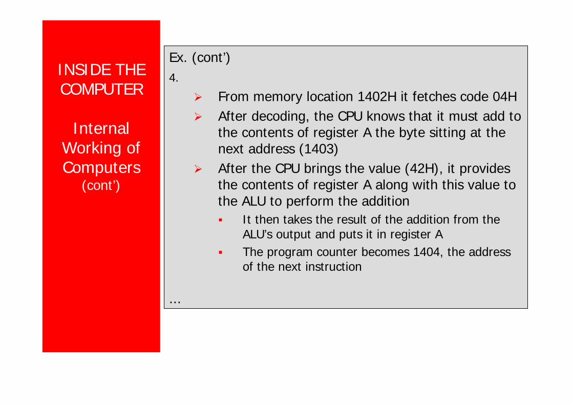
Ex. (cont’)4.
From memory location 1402H it fetches code 04HAfter decoding, the CPU knows that it must add tothe contents of register A the byte sitting at thenext address (1403)After the CPU brings the value (42H), it providesthe contents of register A along with this value tothe ALU to perform the addition
It then takes the result of the addition from theALU’s output and puts it in register AThe program counter becomes 1404, the addressof the next instruction
...
INSIDE THE COMPUTER
Internal Working of Computers
(cont’)
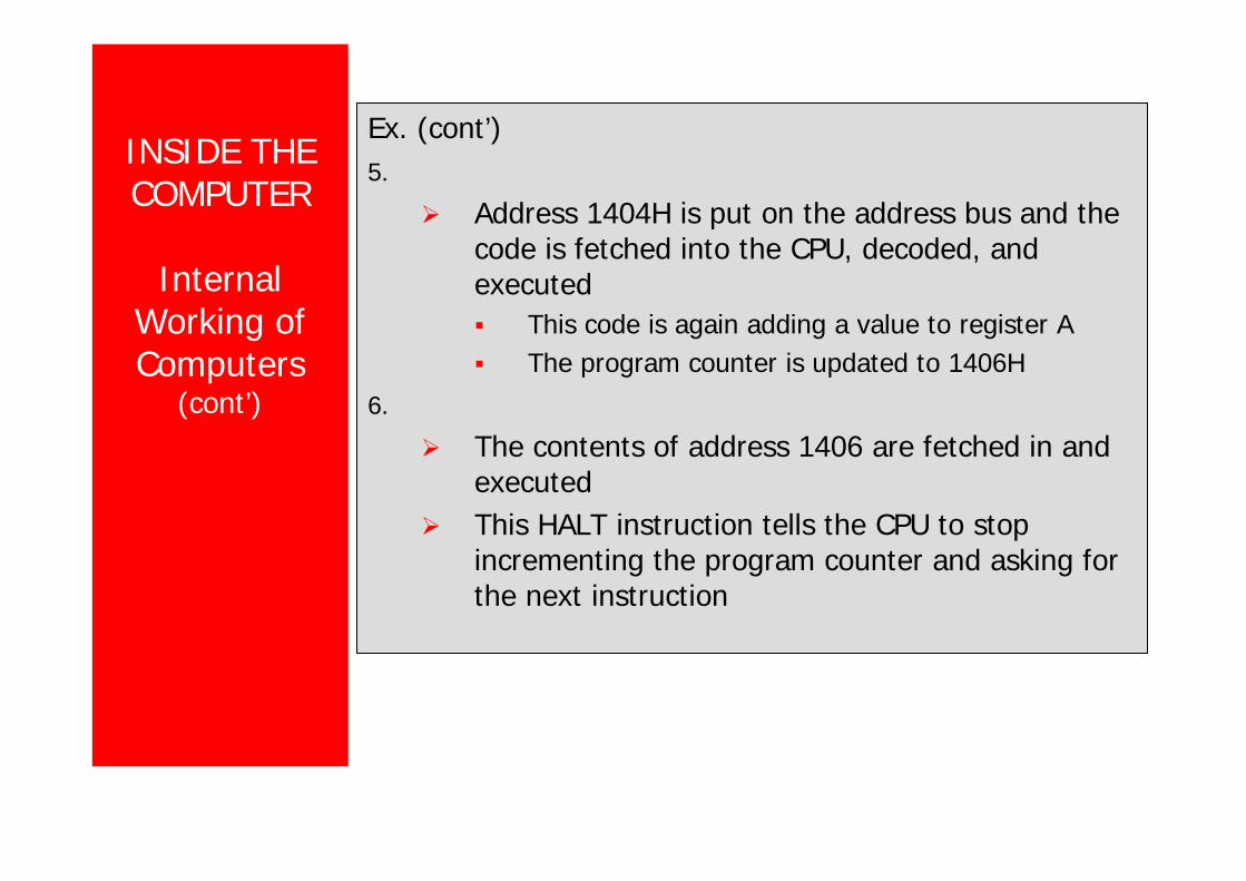
Ex. (cont’)5.
Address 1404H is put on the address bus and thecode is fetched into the CPU, decoded, andexecuted
This code is again adding a value to register AThe program counter is updated to 1406H
6.
The contents of address 1406 are fetched in andexecutedThis HALT instruction tells the CPU to stopincrementing the program counter and asking forthe next instruction
OUTLINES
Microcontrollers and embedded processorsOverview of the 8051 family
8051 MICROCONTROLLERS
MICRO-CONTROLLERS
AND EMBEDDED
PROCESSORS
Microcontroller vs. General-
Purpose Microprocessor
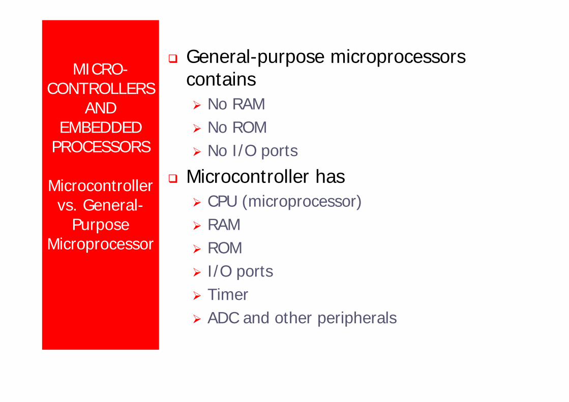
General-purpose microprocessorscontains
No RAMNo ROMNo I/O ports
Microcontroller hasCPU (microprocessor)RAMROMI/O portsTimerADC and other peripherals
MICRO-CONTROLLERS
AND EMBEDDED
PROCESSORS
Microcontroller vs. General-
Purpose Microprocessor
(cont’)
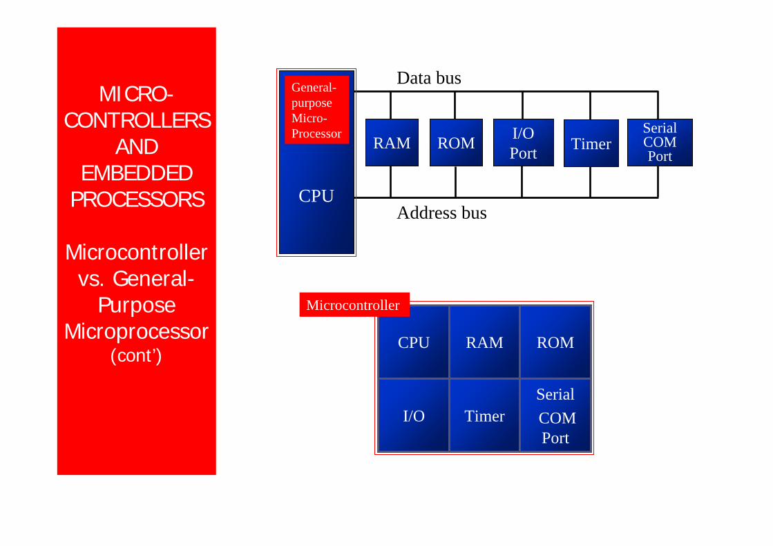
SerialCOM Port
TimerI/O
ROMRAMCPU
Microcontroller
CPU
RAM
Address bus
Data bus
ROM I/O Port
Serial COM Port
Timer
General-purpose Micro-Processor
MICRO-CONTROLLERS
AND EMBEDDED
PROCESSORS
Microcontroller vs. General-
Purpose Microprocessor
(cont’)
General-purpose microprocessorsMust add RAM, ROM, I/O ports, andtimers externally to make them functionalMake the system bulkier and much moreexpensiveHave the advantage of versatility on theamount of RAM, ROM, and I/O ports
MicrocontrollerThe fixed amount of on-chip ROM, RAM,and number of I/O ports makes them idealfor many applications in which cost andspace are criticalIn many applications, the space it takes,the power it consumes, and the price perunit are much more critical considerationsthan the computing power
MICRO-CONTROLLERS
AND EMBEDDED
PROCESSORS
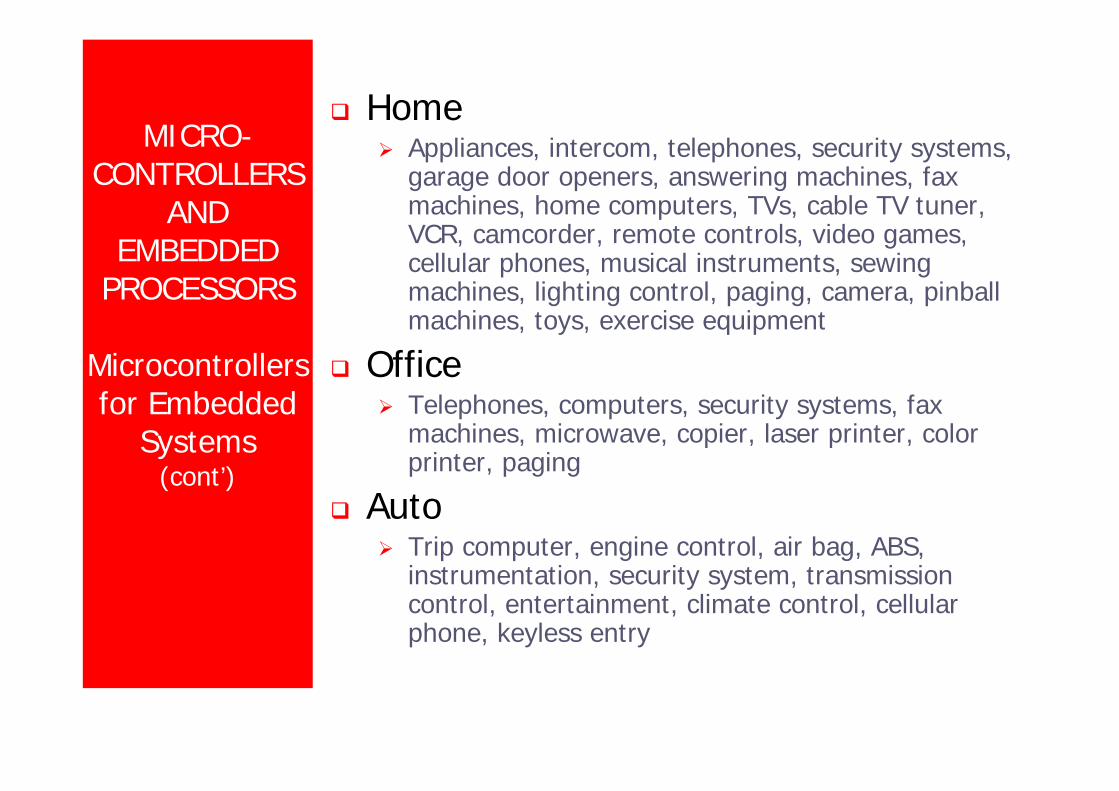
Microcontrollers for Embedded
Systems
An embedded product uses amicroprocessor (or microcontroller) todo one task and one task only
There is only one application software thatis typically burned into ROM
A PC, in contrast with the embeddedsystem, can be used for any number ofapplications
It has RAM memory and an operatingsystem that loads a variety of applicationsinto RAM and lets the CPU run themA PC contains or is connected to variousembedded products
Each one peripheral has a microcontroller insideit that performs only one task
MICRO-CONTROLLERS
AND EMBEDDED
PROCESSORS
Microcontrollers for Embedded
Systems(cont’)
HomeAppliances, intercom, telephones, security systems,garage door openers, answering machines, faxmachines, home computers, TVs, cable TV tuner,VCR, camcorder, remote controls, video games,cellular phones, musical instruments, sewingmachines, lighting control, paging, camera, pinballmachines, toys, exercise equipment
OfficeTelephones, computers, security systems, faxmachines, microwave, copier, laser printer, colorprinter, paging
AutoTrip computer, engine control, air bag, ABS,instrumentation, security system, transmissioncontrol, entertainment, climate control, cellularphone, keyless entry
MICRO-CONTROLLERS
AND EMBEDDED
PROCESSORS
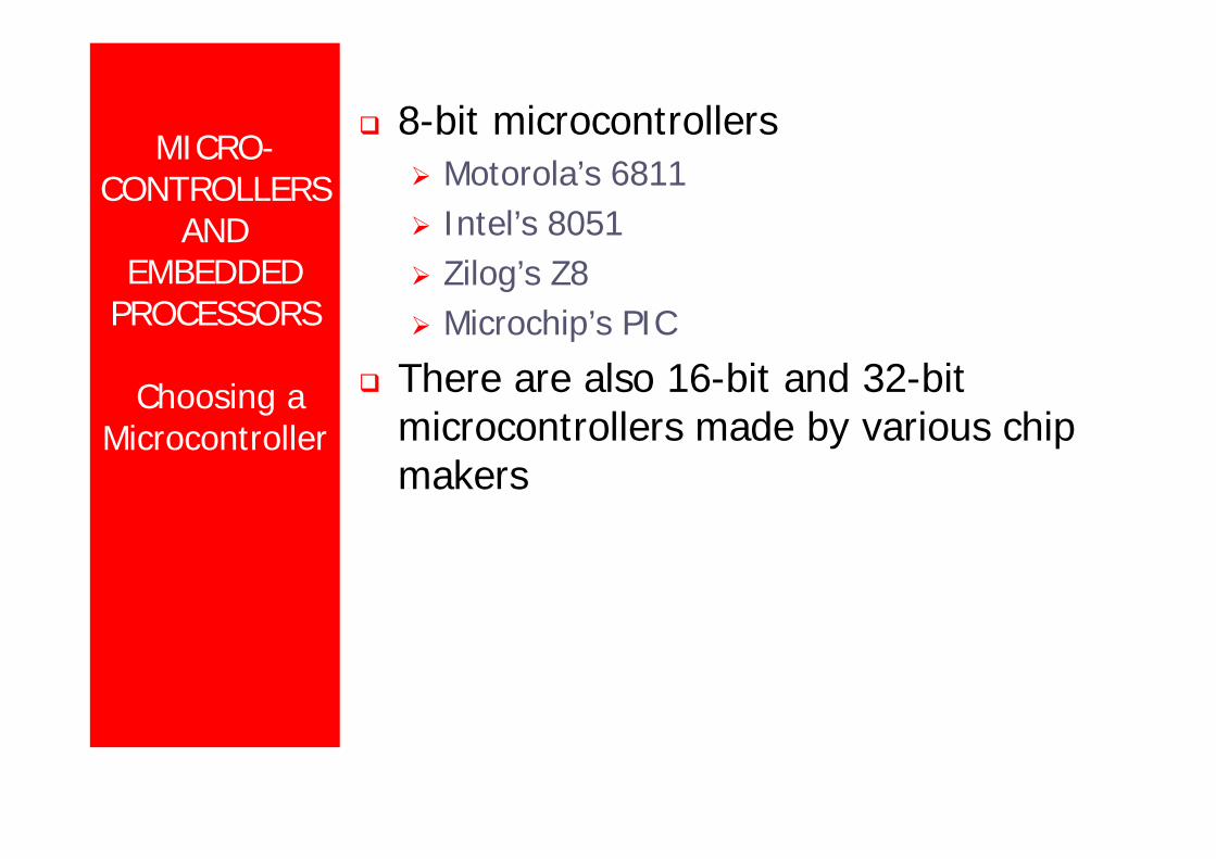
Choosing a Microcontroller
8-bit microcontrollersMotorola’s 6811Intel’s 8051Zilog’s Z8Microchip’s PIC
There are also 16-bit and 32-bitmicrocontrollers made by various chipmakers
MICRO-CONTROLLERS
AND EMBEDDED
PROCESSORS
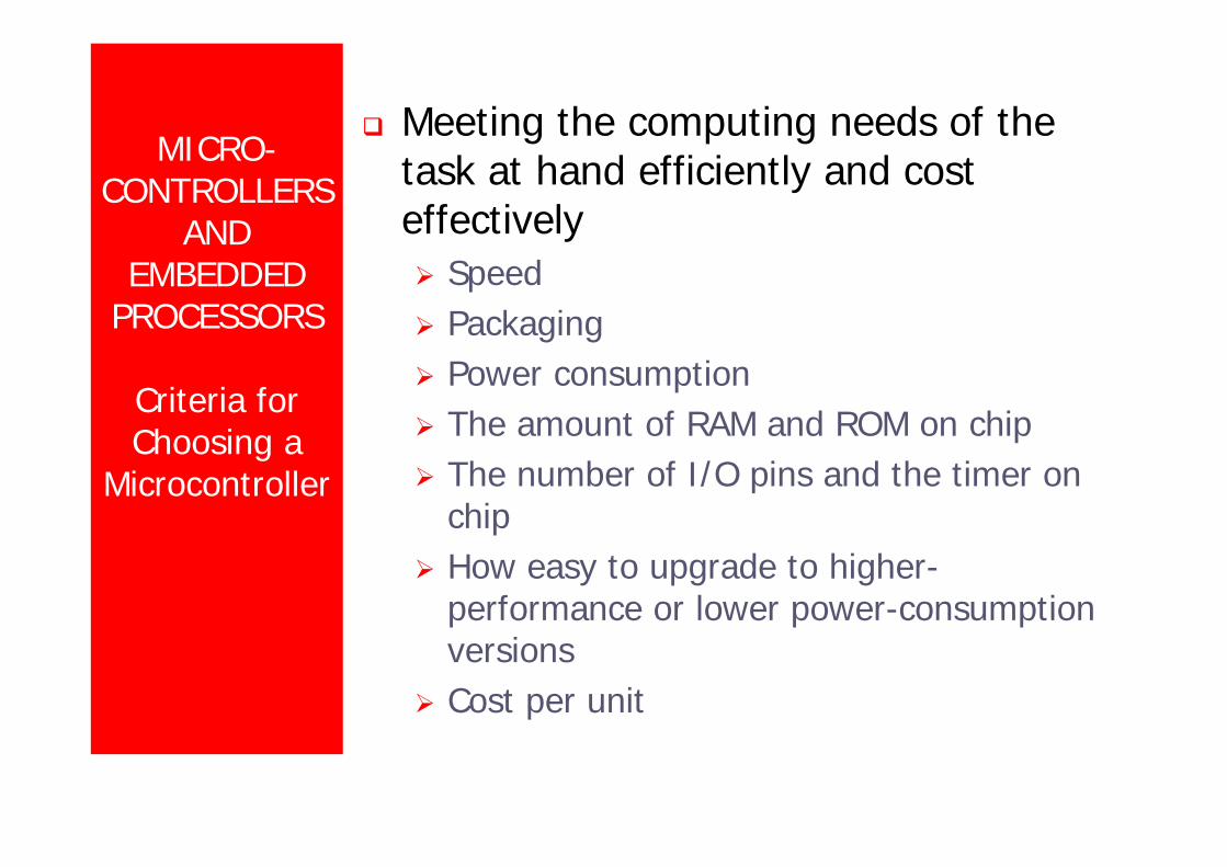
Criteria for Choosing a
Microcontroller
Meeting the computing needs of thetask at hand efficiently and costeffectively
SpeedPackagingPower consumptionThe amount of RAM and ROM on chipThe number of I/O pins and the timer onchipHow easy to upgrade to higher-performance or lower power-consumptionversionsCost per unit
MICRO-CONTROLLERS
AND EMBEDDED
PROCESSORS
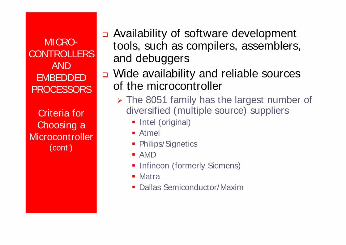
Criteria for Choosing a
Microcontroller (cont’)
Availability of software developmenttools, such as compilers, assemblers,and debuggersWide availability and reliable sourcesof the microcontroller
The 8051 family has the largest number ofdiversified (multiple source) suppliers
Intel (original)AtmelPhilips/SigneticsAMDInfineon (formerly Siemens)MatraDallas Semiconductor/Maxim
OVERVIEW OF 8051 FAMILY
8051 Microcontroller
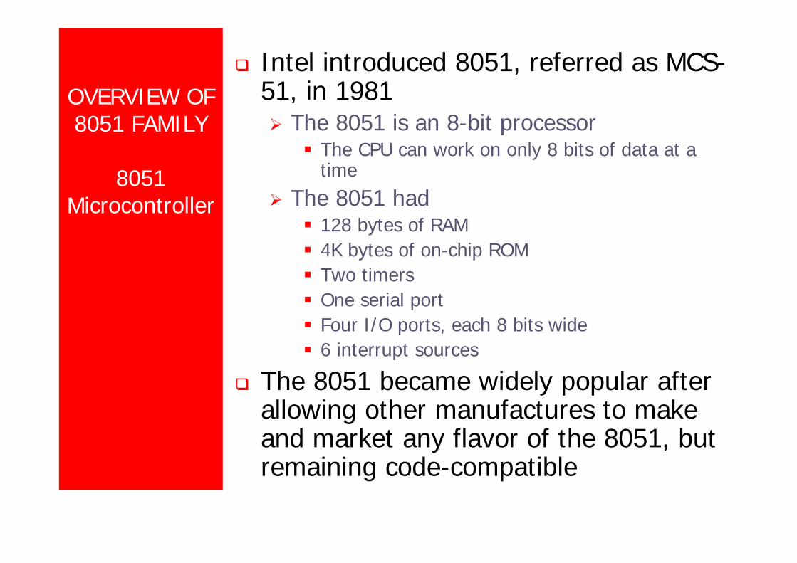
Intel introduced 8051, referred as MCS-51, in 1981
The 8051 is an 8-bit processorThe CPU can work on only 8 bits of data at atime
The 8051 had128 bytes of RAM4K bytes of on-chip ROMTwo timersOne serial portFour I/O ports, each 8 bits wide6 interrupt sources
The 8051 became widely popular afterallowing other manufactures to makeand market any flavor of the 8051, butremaining code-compatible
PIN DESCRIPTION
(cont’)
8051/52(DS89C4x0AT89C518031)
P1.0
P1.1
P1.2
P1.3
P1.4
P1.5
P1.6
P1.7
RST
(RXD)P3.0
(TXD)P3.1
(-INT0)P3.2
(-INT1)P3.3
(T0)P3.4
(T1)P3.5
(-WR)P3.6
(-RD)P3.7
XTAL2
XTAL1
GND
Vcc
P0.0(AD0)
P0.1(AD1)
P0.2(AD2)
P0.3(AD3)
P0.4(AD4)
P0.5(AD5)
P0.6(AD6)
P0.7(AD7)
-EA/VPP
ALE/-PROG
-PSEN
P2.7(A15)
P2.6(A14)
P2.5(A13)
P2.4(A12)
P2.3(A11)
P2.2(A10)
P2.1(A9)
P2.0(A8)
1
2
3
4
5
6
7
8
9
10
11
12
13
14
15
16
17
18
19
20
40
39
38
37
36
35
34
33
32
31
30
29
28
27
26
25
24
23
22
21
8051 pin diagram
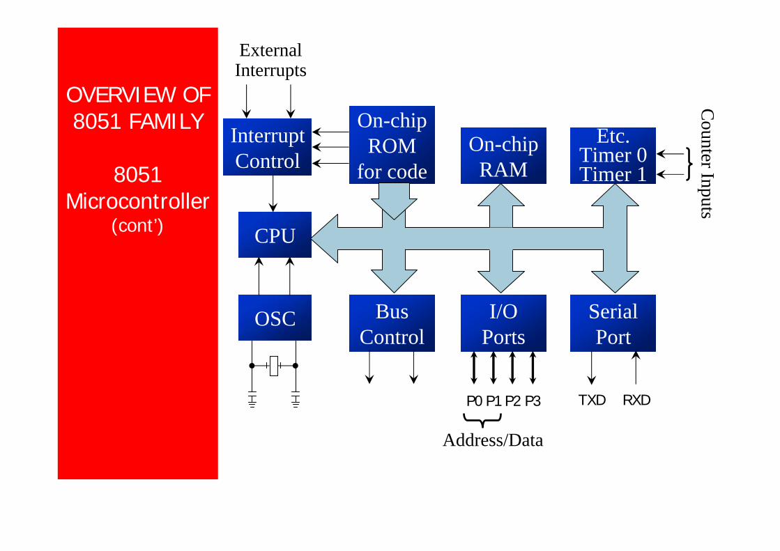
OVERVIEW OF 8051 FAMILY
8051 Microcontroller
(cont’)
Interrupt Control
Bus Control
CPU
OSC I/O Ports
Serial Port
Etc.Timer 0Timer 1
On-chip RAM
On-chip ROM
for code
P0 P1 P2 P3
Address/Data
TXD RXD
Counter Inputs
External Interrupts
INSIDE THE 8051
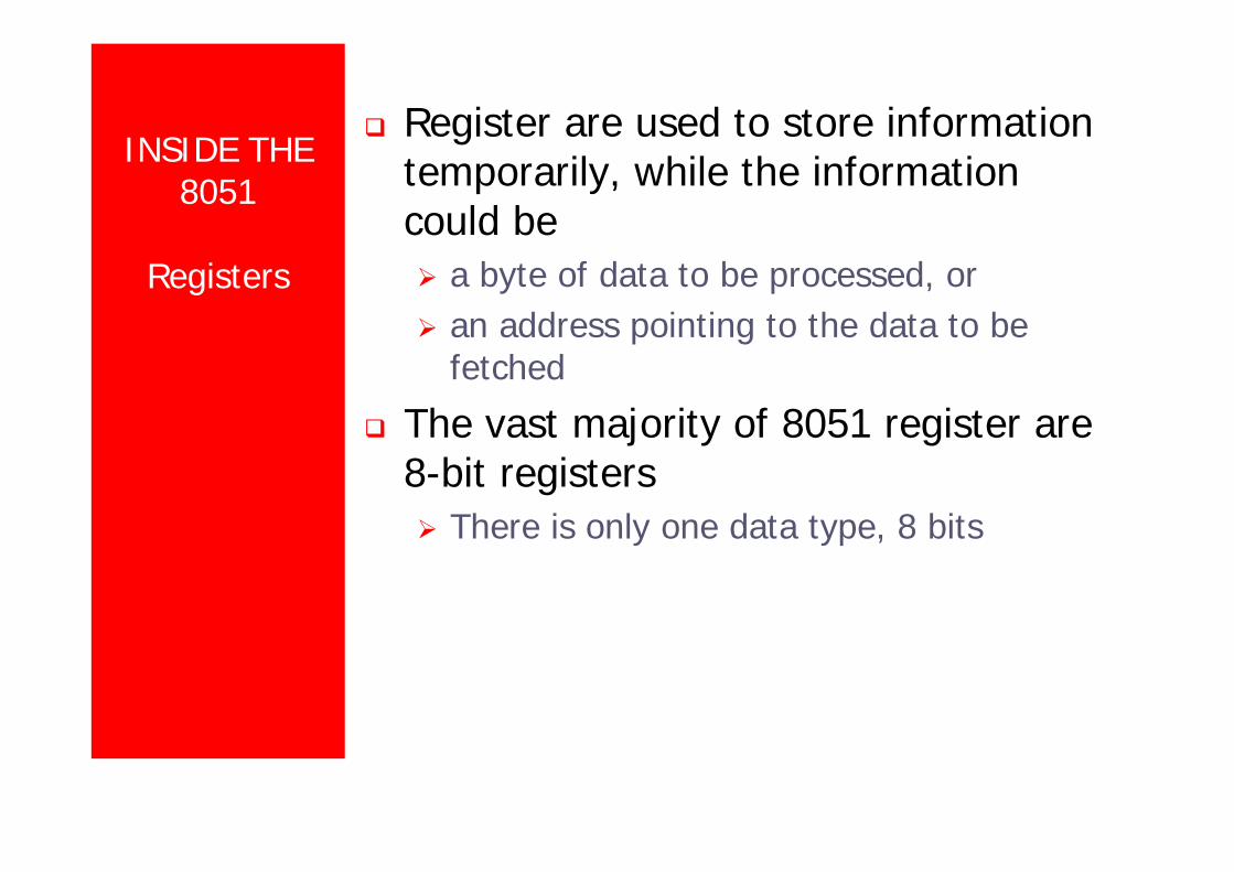
Registers
Register are used to store informationtemporarily, while the informationcould be
a byte of data to be processed, oran address pointing to the data to befetched
The vast majority of 8051 register are8-bit registers
There is only one data type, 8 bits
INSIDE THE 8051
Registers(cont’)
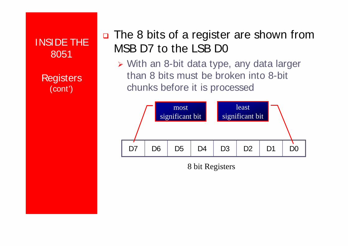
The 8 bits of a register are shown fromMSB D7 to the LSB D0
With an 8-bit data type, any data largerthan 8 bits must be broken into 8-bitchunks before it is processed
D0D1D2D3D4D5D6D7
8 bit Registers
most significant bit
least significant bit
INSIDE THE 8051
Registers(cont’)
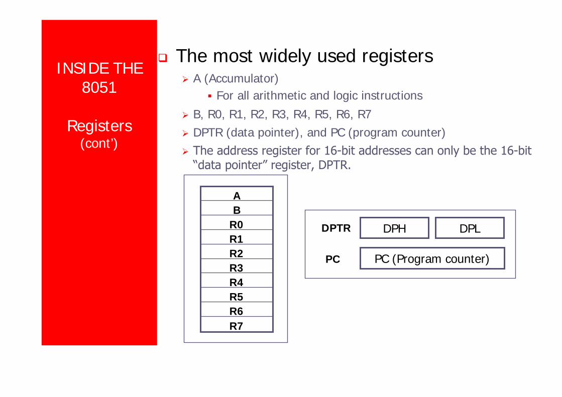
The most widely used registersA (Accumulator)
For all arithmetic and logic instructions
B, R0, R1, R2, R3, R4, R5, R6, R7DPTR (data pointer), and PC (program counter)The address register for 16-bit addresses can only be the 16-bit“data pointer” register, DPTR.
R6R5R4R3R2R1R0BA
R7
DPTR
PC PC (Program counter)
DPH DPL
INSIDE THE 8051
MOV Instruction
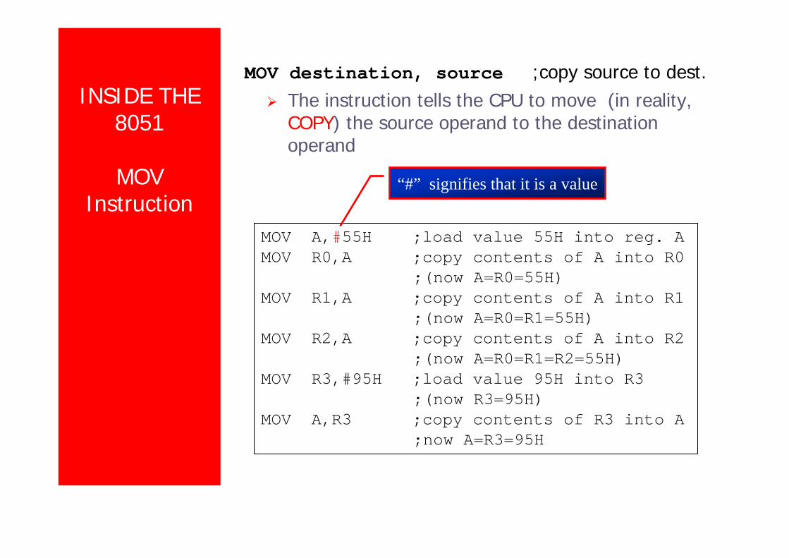
MOV destination, source ;copy source to dest.The instruction tells the CPU to move (in reality,COPY) the source operand to the destinationoperand
MOV A,#55H ;load value 55H into reg. AMOV R0,A ;copy contents of A into R0
;(now A=R0=55H)MOV R1,A ;copy contents of A into R1
;(now A=R0=R1=55H)MOV R2,A ;copy contents of A into R2
;(now A=R0=R1=R2=55H)MOV R3,#95H ;load value 95H into R3
;(now R3=95H)MOV A,R3 ;copy contents of R3 into A
;now A=R3=95H
“#” signifies that it is a value
INSIDE THE 8051
MOV Instruction
(cont’)
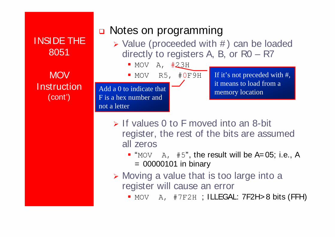
Notes on programmingValue (proceeded with #) can be loadeddirectly to registers A, B, or R0 – R7
MOV A, #23HMOV R5, #0F9H
If values 0 to F moved into an 8-bitregister, the rest of the bits are assumedall zeros
“MOV A, #5”, the result will be A=05; i.e., A= 00000101 in binary
Moving a value that is too large into aregister will cause an error
MOV A, #7F2H ; ILLEGAL: 7F2H>8 bits (FFH)
If it’s not preceded with #, it means to load from a memory locationAdd a 0 to indicate that
F is a hex number and not a letter
INSIDE THE 8051
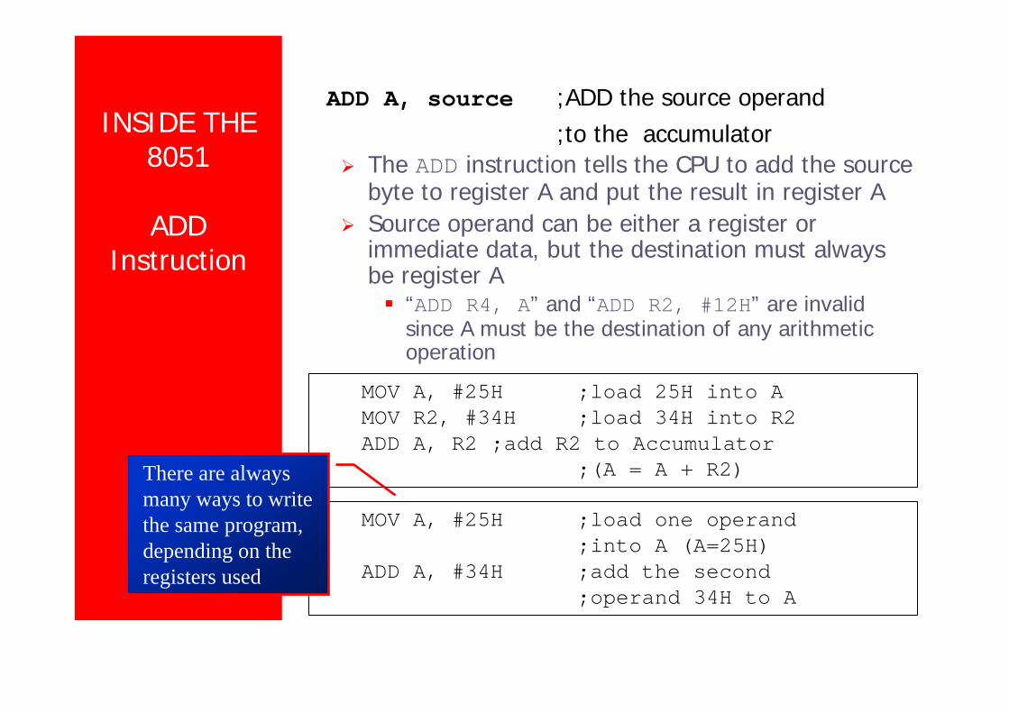
ADD Instruction
ADD A, source ;ADD the source operand ;to the accumulator
The ADD instruction tells the CPU to add the sourcebyte to register A and put the result in register ASource operand can be either a register orimmediate data, but the destination must alwaysbe register A
“ADD R4, A” and “ADD R2, #12H” are invalidsince A must be the destination of any arithmeticoperation
MOV A, #25H ;load 25H into AMOV R2, #34H ;load 34H into R2ADD A, R2 ;add R2 to Accumulator
;(A = A + R2)
MOV A, #25H ;load one operand ;into A (A=25H)
ADD A, #34H ;add the second ;operand 34H to A
There are always many ways to write the same program, depending on the registers used
Structure of Assembly Language
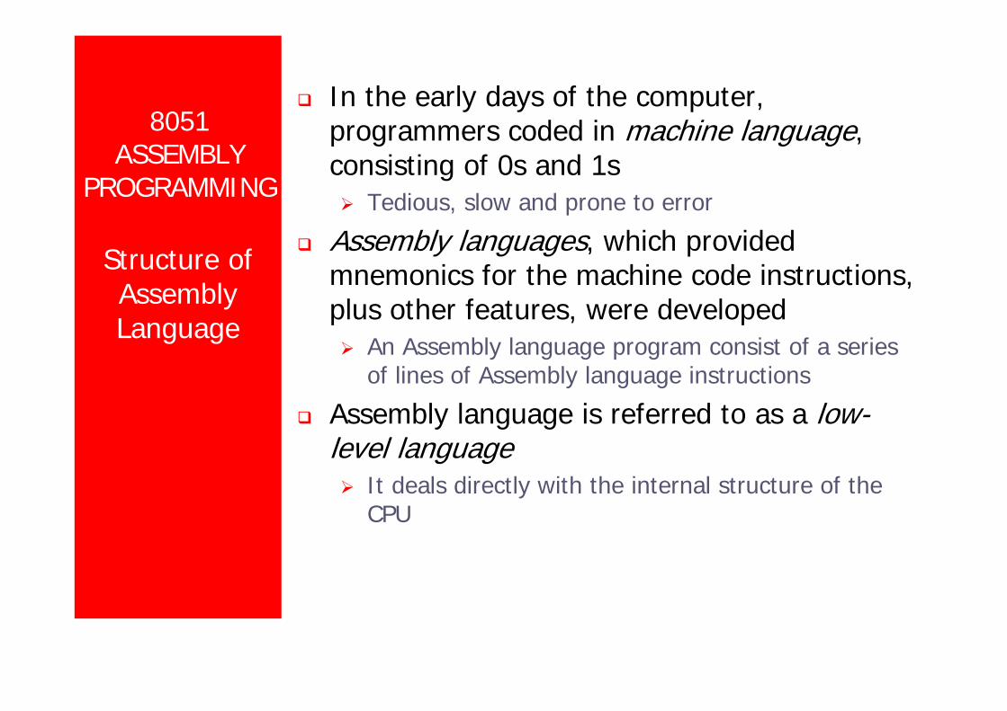
In the early days of the computer,programmers coded in machine language,consisting of 0s and 1s
Tedious, slow and prone to error
Assembly languages, which providedmnemonics for the machine code instructions,plus other features, were developed
An Assembly language program consist of a seriesof lines of Assembly language instructions
Assembly language is referred to as a low-level language
It deals directly with the internal structure of theCPU
8051 ASSEMBLY
PROGRAMMING
Structure of Assembly Language
8051 ASSEMBLY
PROGRAMMING
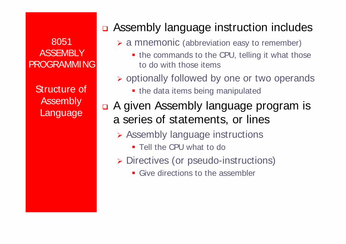
Assembly language instruction includesa mnemonic (abbreviation easy to remember)
the commands to the CPU, telling it what thoseto do with those items
optionally followed by one or two operandsthe data items being manipulated
A given Assembly language program isa series of statements, or lines
Assembly language instructionsTell the CPU what to do
Directives (or pseudo-instructions)Give directions to the assembler
Structure of Assembly Language
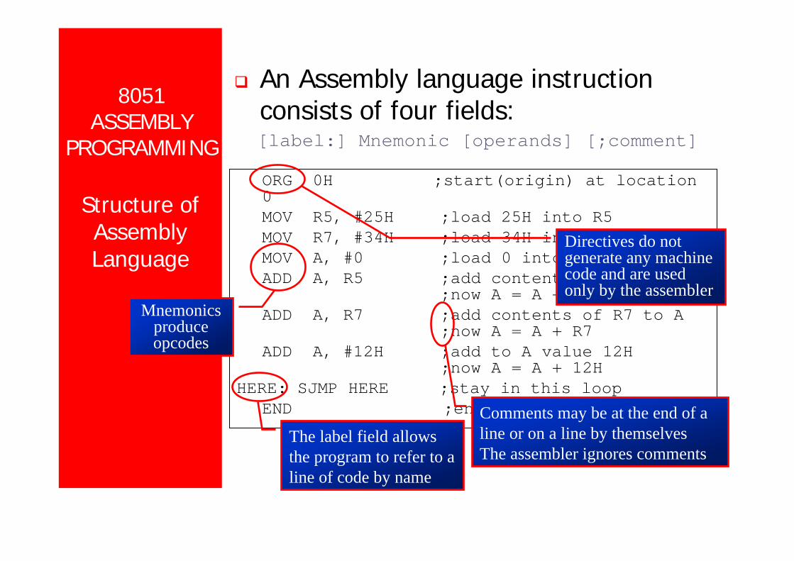
ORG 0H ;start(origin) at location 0MOV R5, #25H ;load 25H into R5MOV R7, #34H ;load 34H into R7MOV A, #0 ;load 0 into AADD A, R5 ;add contents of R5 to A
;now A = A + R5ADD A, R7 ;add contents of R7 to A
;now A = A + R7ADD A, #12H ;add to A value 12H
;now A = A + 12HHERE: SJMP HERE ;stay in this loop
END ;end of asm source file
8051 ASSEMBLY
PROGRAMMING
An Assembly language instructionconsists of four fields:[label:] Mnemonic [operands] [;comment]
Mnemonics produce opcodes
The label field allows the program to refer to a line of code by name
Comments may be at the end of a line or on a line by themselvesThe assembler ignores comments
Directives do not generate any machine code and are used only by the assembler
ASSEMBLING AND RUNNING
AN 8051 PROGRAM
The step of Assembly languageprogram are outlines as follows:
1) First we use an editor to type a program,many excellent editors or wordprocessors are available that can be usedto create and/or edit the program
Notice that the editor must be able to producean ASCII fileFor many assemblers, the file names followthe usual DOS conventions, but the source filehas the extension “asm“ or “src”, dependingon which assembly you are using
ASSEMBLING AND RUNNING
AN 8051 PROGRAM
(cont’)
2) The “asm” source file containing theprogram code created in step 1 is fed toan 8051 assembler
The assembler converts the instructions intomachine codeThe assembler will produce an object file anda list fileThe extension for the object file is “obj” whilethe extension for the list file is “lst”
3) Assembler require a third step calledlinking
The linker program takes one or more objectcode files and produce an absolute object filewith the extension “abs”This abs file is used by 8051 trainers thathave a monitor program
ASSEMBLING AND RUNNING
AN 8051 PROGRAM
(cont’)
4) Next the “abs” file is fed into a programcalled “OH” (object to hex converter)which creates a file with extension “hex”that is ready to burn into ROM
This program comes with all 8051 assemblersRecent Windows-based assemblers combinestep 2 through 4 into one step
ASSEMBLING AND RUNNING
AN 8051 PROGRAM
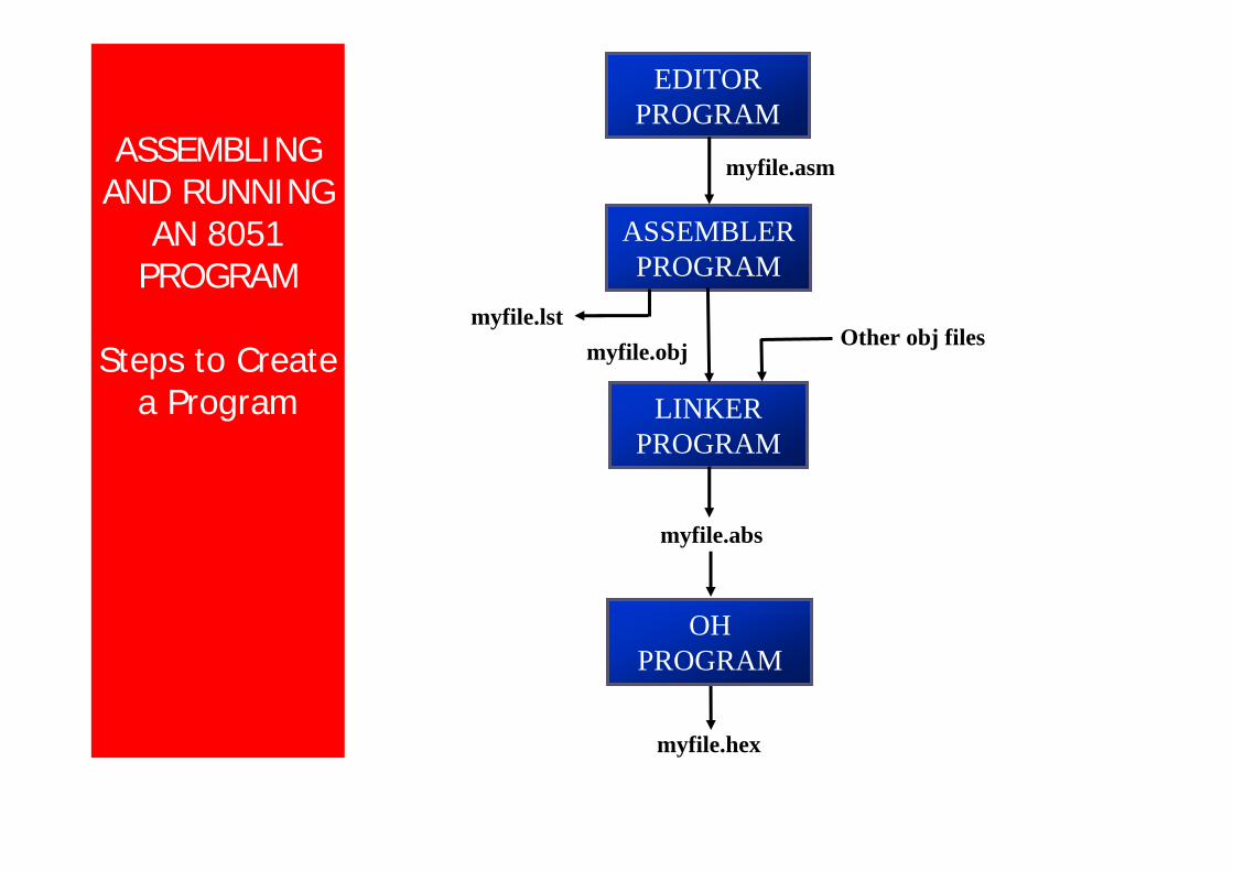
Steps to Create a Program
EDITOR PROGRAM
ASSEMBLER PROGRAM
LINKER PROGRAM
OH PROGRAM
myfile.asm
myfile.obj
myfile.abs
myfile.lstOther obj files
myfile.hex
Department of Computer Science and Information EngineeringNational Cheng Kung University, TAIWAN
ASSEMBLING AND RUNNING
AN 8051 PROGRAM
lst File
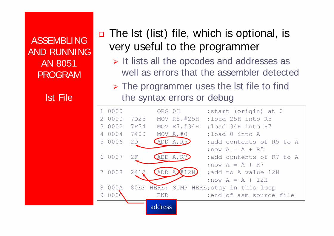
The lst (list) file, which is optional, isvery useful to the programmer
It lists all the opcodes and addresses aswell as errors that the assembler detectedThe programmer uses the lst file to findthe syntax errors or debug
1 0000 ORG 0H ;start (origin) at 02 0000 7D25 MOV R5,#25H ;load 25H into R53 0002 7F34 MOV R7,#34H ;load 34H into R74 0004 7400 MOV A,#0 ;load 0 into A5 0006 2D ADD A,R5 ;add contents of R5 to A
;now A = A + R56 0007 2F ADD A,R7 ;add contents of R7 to A
;now A = A + R77 0008 2412 ADD A,#12H ;add to A value 12H
;now A = A + 12H8 000A 80EF HERE: SJMP HERE;stay in this loop9 000C END ;end of asm source file
address
PROGRAM COUNTER AND
ROM SPACE
Program Counter
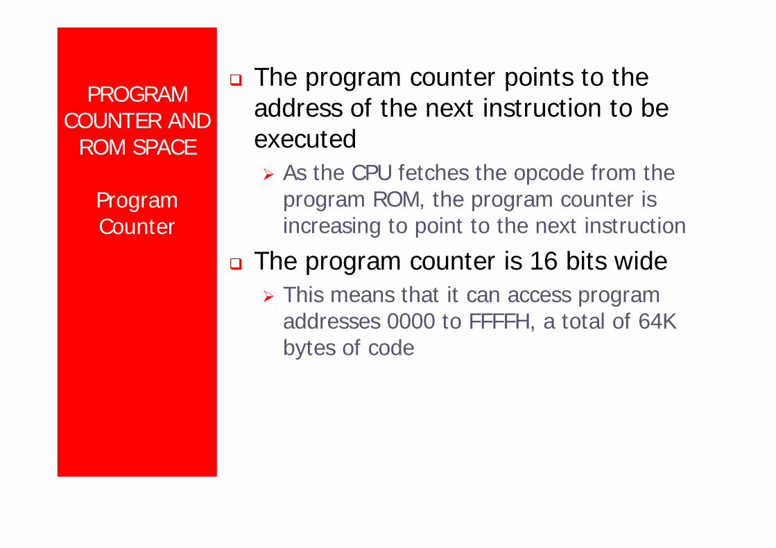
The program counter points to theaddress of the next instruction to beexecuted
As the CPU fetches the opcode from theprogram ROM, the program counter isincreasing to point to the next instruction
The program counter is 16 bits wideThis means that it can access programaddresses 0000 to FFFFH, a total of 64Kbytes of code
PROGRAM COUNTER AND
ROM SPACE
Power up
All 8051 members start at memoryaddress 0000 when they’re poweredup
Program Counter has the value of 0000The first opcode is burned into ROMaddress 0000H, since this is where the8051 looks for the first instruction when itis bootedWe achieve this by the ORG statement inthe source program
PROGRAM COUNTER AND
ROM SPACE
Placing Code in ROM
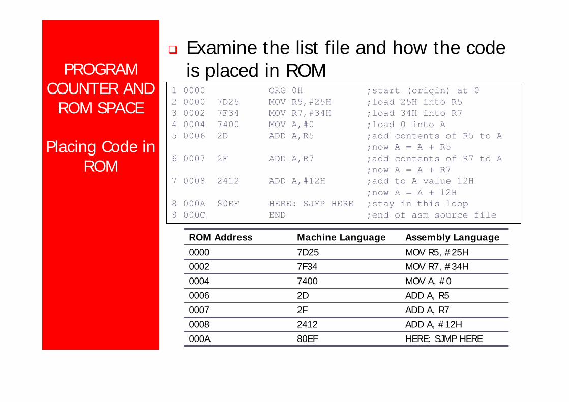
Examine the list file and how the codeis placed in ROM
1 0000 ORG 0H ;start (origin) at 02 0000 7D25 MOV R5,#25H ;load 25H into R53 0002 7F34 MOV R7,#34H ;load 34H into R74 0004 7400 MOV A,#0 ;load 0 into A5 0006 2D ADD A,R5 ;add contents of R5 to A
;now A = A + R56 0007 2F ADD A,R7 ;add contents of R7 to A
;now A = A + R77 0008 2412 ADD A,#12H ;add to A value 12H
;now A = A + 12H8 000A 80EF HERE: SJMP HERE ;stay in this loop9 000C END ;end of asm source file
HERE: SJMP HERE80EF000AADD A, #12H24120008ADD A, R72F0007ADD A, R52D0006MOV A, #074000004MOV R7, #34H7F340002MOV R5, #25H7D250000
Assembly LanguageMachine LanguageROM Address
PROGRAM COUNTER AND
ROM SPACE
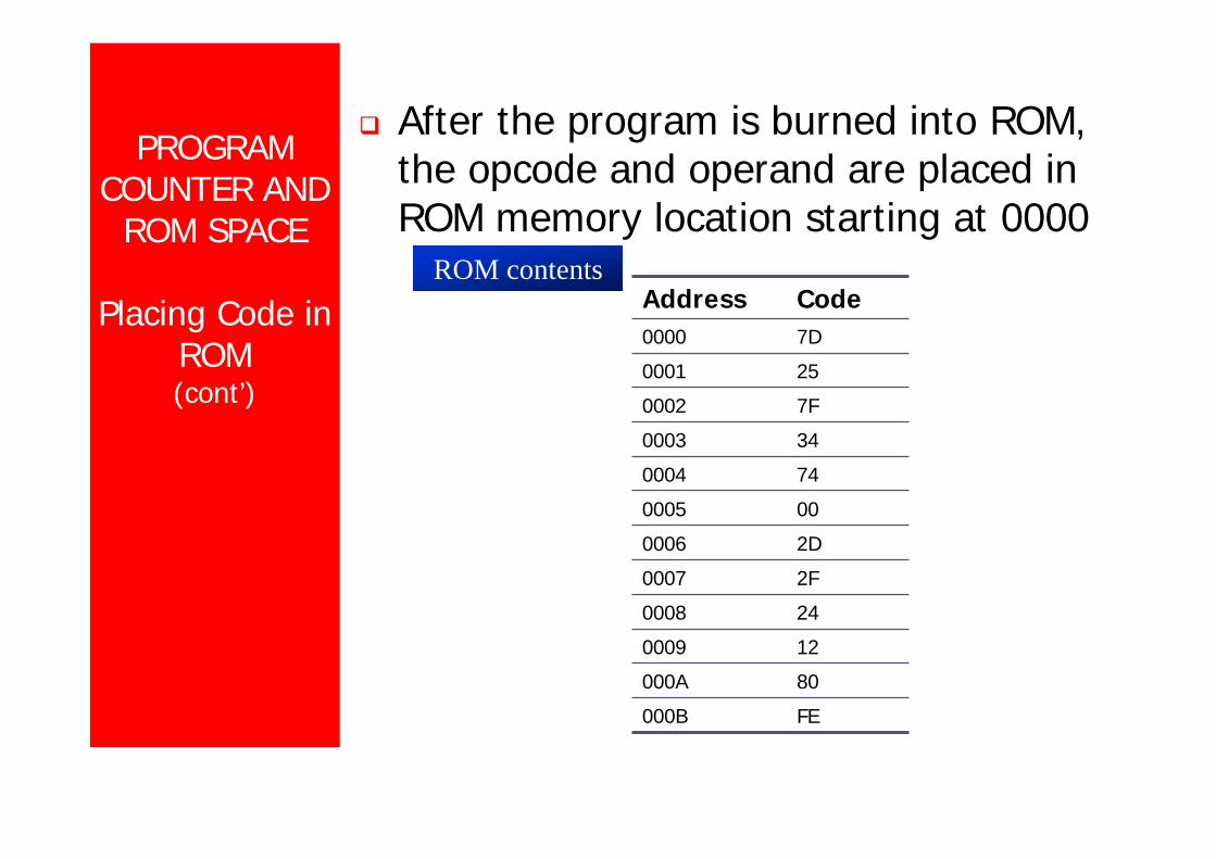
Placing Code in ROM(cont’)
After the program is burned into ROM,the opcode and operand are placed inROM memory location starting at 0000
FE000B
80000A
120009
240008
2F0007
2D0006
000005
740004
340003
7F0002
250001
7D0000
CodeAddressROM contents
PROGRAM COUNTER AND
ROM SPACE
Executing Program
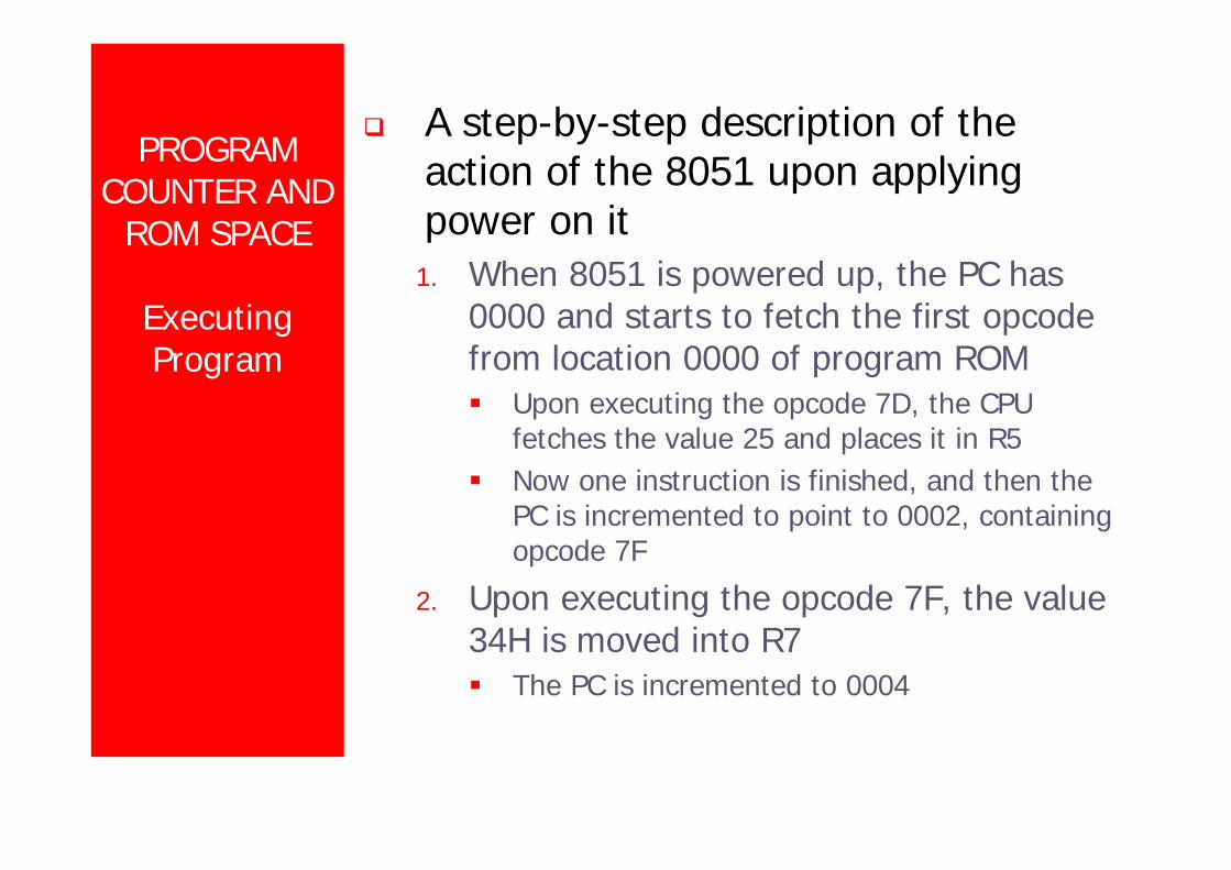
A step-by-step description of theaction of the 8051 upon applyingpower on it
1. When 8051 is powered up, the PC has0000 and starts to fetch the first opcodefrom location 0000 of program ROM
Upon executing the opcode 7D, the CPUfetches the value 25 and places it in R5Now one instruction is finished, and then thePC is incremented to point to 0002, containingopcode 7F
2. Upon executing the opcode 7F, the value34H is moved into R7
The PC is incremented to 0004
PROGRAM COUNTER AND
ROM SPACE
Executing Program
(cont’)
(cont’)
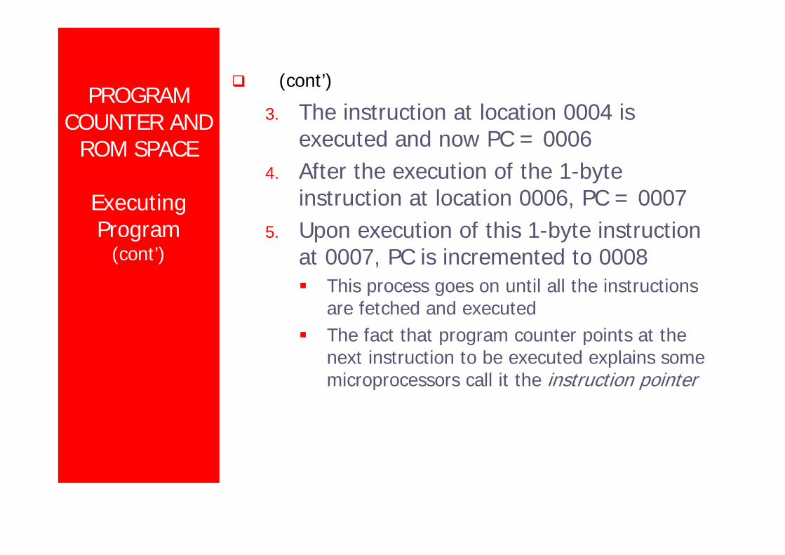
3. The instruction at location 0004 isexecuted and now PC = 0006
4. After the execution of the 1-byteinstruction at location 0006, PC = 0007
5. Upon execution of this 1-byte instructionat 0007, PC is incremented to 0008
This process goes on until all the instructionsare fetched and executedThe fact that program counter points at thenext instruction to be executed explains somemicroprocessors call it the instruction pointer
8051 DATA TYPES AND DIRECTIVES
Data Type
8051 microcontroller has only one datatype - 8 bits
The size of each register is also 8 bitsIt is the job of the programmer to breakdown data larger than 8 bits (00 to FFH,or 0 to 255 in decimal)The data types can be positive or negative
8051 DATA TYPES AND DIRECTIVES
Assembler Directives
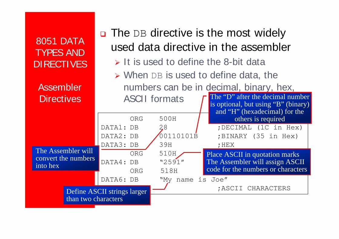
The DB directive is the most widelyused data directive in the assembler
It is used to define the 8-bit dataWhen DB is used to define data, thenumbers can be in decimal, binary, hex,ASCII formats
ORG 500HDATA1: DB 28 ;DECIMAL (1C in Hex)DATA2: DB 00110101B ;BINARY (35 in Hex)DATA3: DB 39H ;HEX
ORG 510HDATA4: DB “2591” ;ASCII NUMBERS
ORG 518HDATA6: DB “My name is Joe”
;ASCII CHARACTERS
The “D” after the decimal number is optional, but using “B” (binary)
and “H” (hexadecimal) for the others is required
The Assembler will convert the numbers into hex
Place ASCII in quotation marksThe Assembler will assign ASCII code for the numbers or characters
Define ASCII strings larger than two characters
8051 DATA TYPES AND DIRECTIVES
Assembler Directives
(cont’)
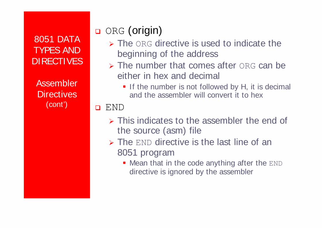
ORG (origin)The ORG directive is used to indicate thebeginning of the addressThe number that comes after ORG can beeither in hex and decimal
If the number is not followed by H, it is decimaland the assembler will convert it to hex
ENDThis indicates to the assembler the end ofthe source (asm) fileThe END directive is the last line of an8051 program
Mean that in the code anything after the ENDdirective is ignored by the assembler

8051 DATA TYPES AND DIRECTIVES
Assembler directives
(cont’)
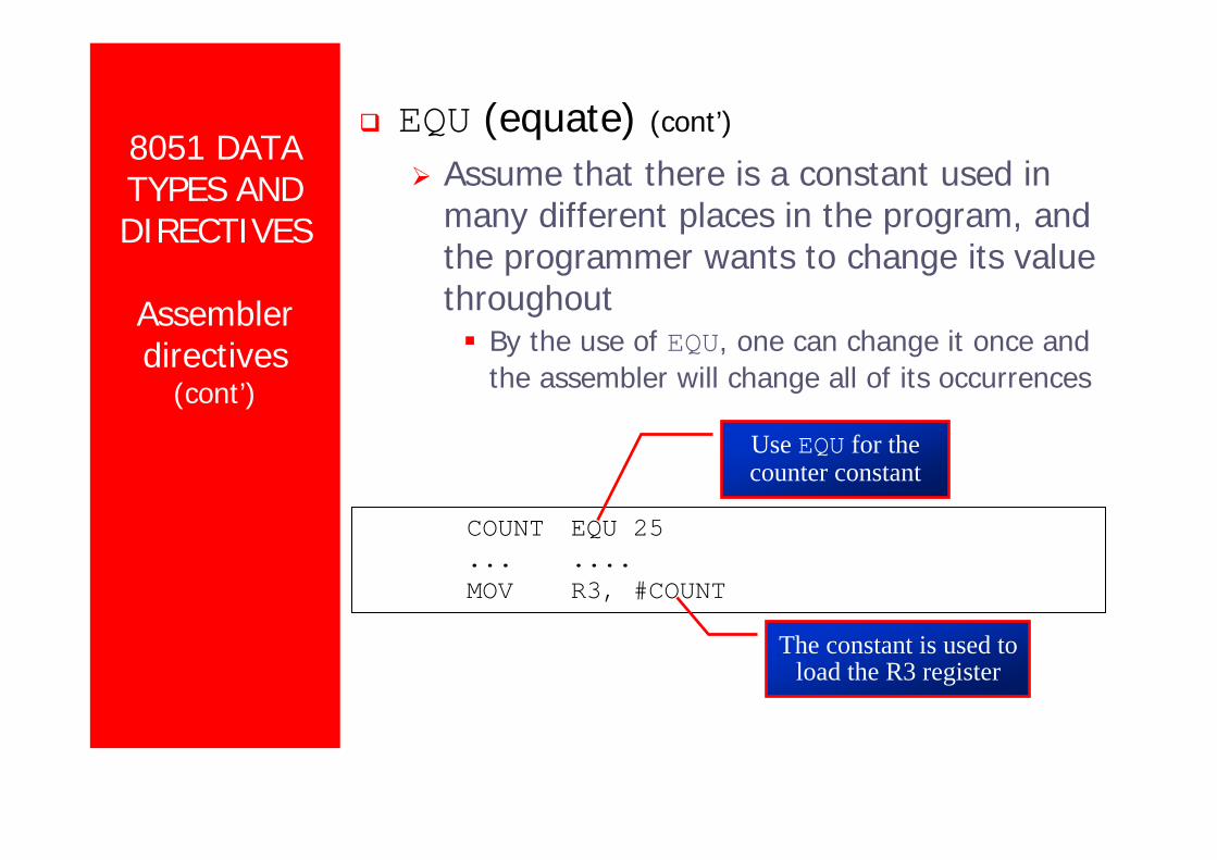
EQU (equate)This is used to define a constant withoutoccupying a memory locationThe EQU directive does not set asidestorage for a data item but associates aconstant value with a data label
When the label appears in the program, itsconstant value will be substituted for the label
8051 DATA TYPES AND DIRECTIVES
Assembler directives
(cont’)
EQU (equate) (cont’)
Assume that there is a constant used inmany different places in the program, andthe programmer wants to change its valuethroughout
By the use of EQU, one can change it once andthe assembler will change all of its occurrences
COUNT EQU 25... ....MOV R3, #COUNT
Use EQU for the counter constant
The constant is used to load the R3 register
FLAG BITS AND PSW REGISTER
Program Status Word
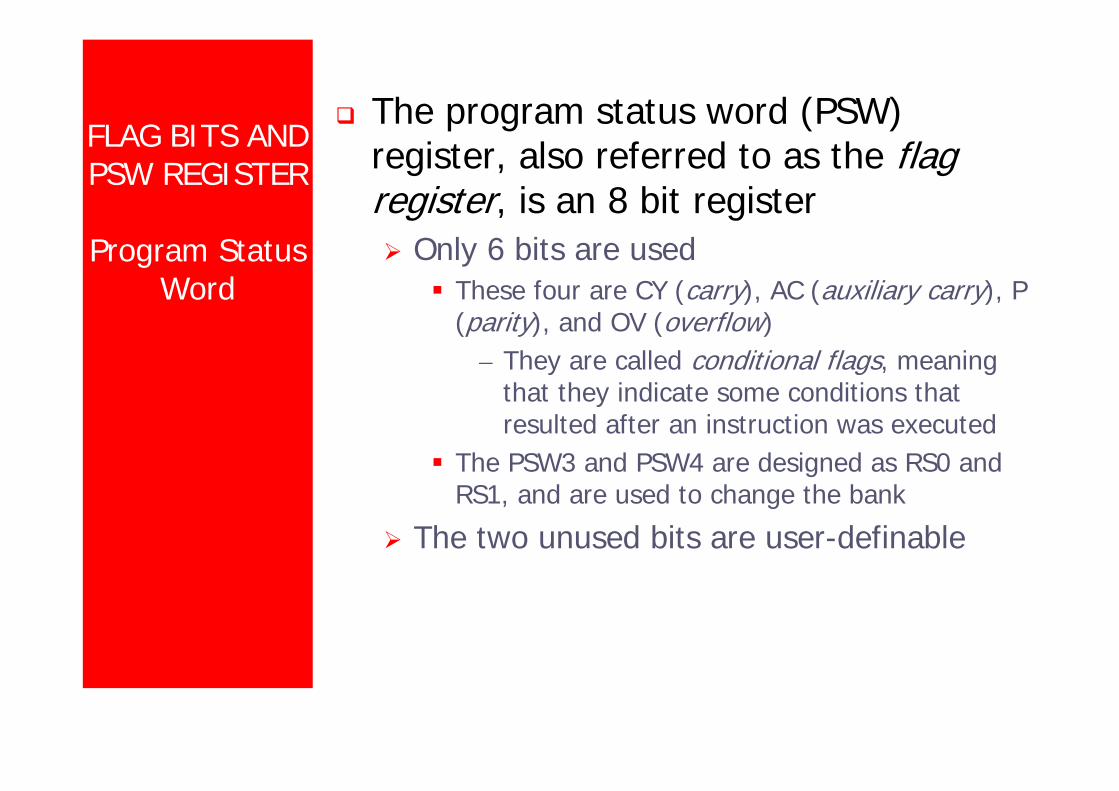
The program status word (PSW)register, also referred to as the flag register, is an 8 bit register
Only 6 bits are usedThese four are CY (carry), AC (auxiliary carry), P(parity), and OV (overflow)
– They are called conditional flags, meaningthat they indicate some conditions thatresulted after an instruction was executed
The PSW3 and PSW4 are designed as RS0 andRS1, and are used to change the bank
The two unused bits are user-definable
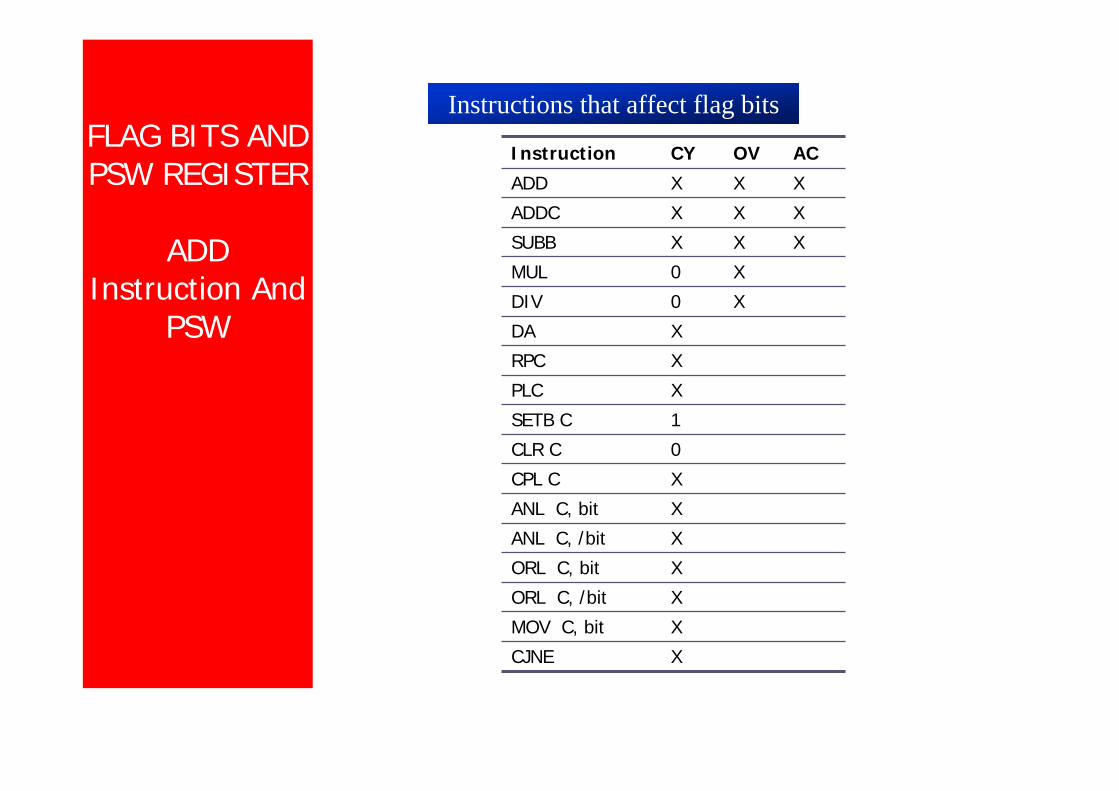
FLAG BITS AND PSW REGISTER
ADD Instruction And
PSW
XCJNE
XMOV C, bit
XORL C, /bit
XORL C, bit
XANL C, /bit
XANL C, bit
XCPL C
0CLR C
1SETB C
XPLC
XRPC
XDA
X0DIV
X0MUL
XXXSUBB
XXXADDC
XXXADD
ACOVCYInstruction
Instructions that affect flag bits
REGISTER BANKS AND
STACK
RAM Memory Space
Allocation
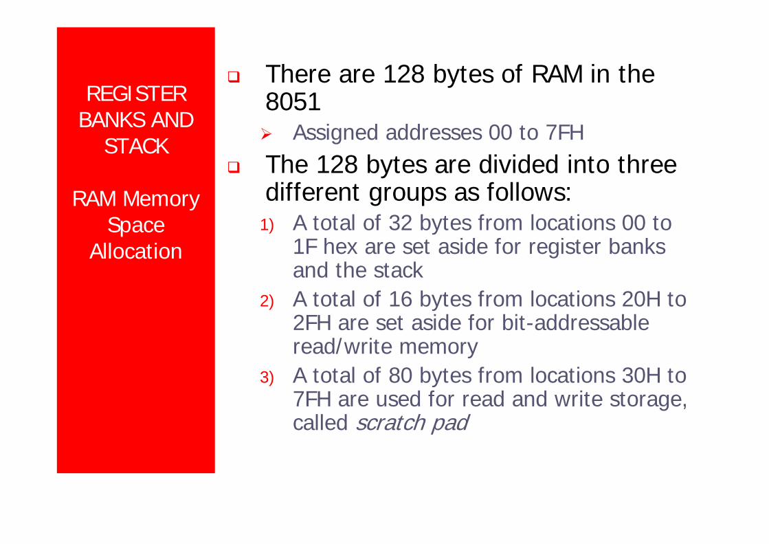
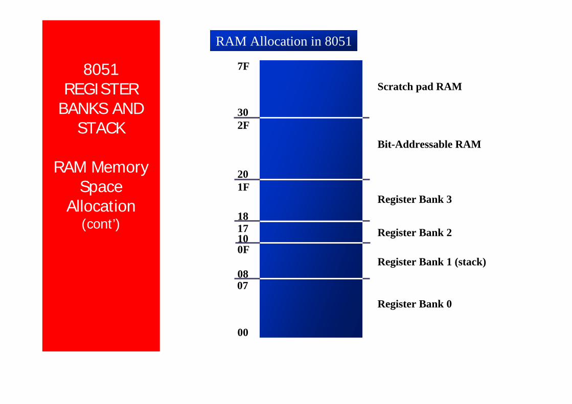
There are 128 bytes of RAM in the8051
Assigned addresses 00 to 7FHThe 128 bytes are divided into threedifferent groups as follows:
1) A total of 32 bytes from locations 00 to1F hex are set aside for register banksand the stack
2) A total of 16 bytes from locations 20H to2FH are set aside for bit-addressableread/write memory
3) A total of 80 bytes from locations 30H to7FH are used for read and write storage,called scratch pad
8051 REGISTER
BANKS AND STACK
RAM Memory Space
Allocation(cont’)
Scratch pad RAM
Bit-Addressable RAM
Register Bank 3
Register Bank 2
Register Bank 1 (stack)
Register Bank 0
00
0708
0F101718
1F20
2F30
7F
RAM Allocation in 8051
8051 REGISTER
BANKS AND STACK
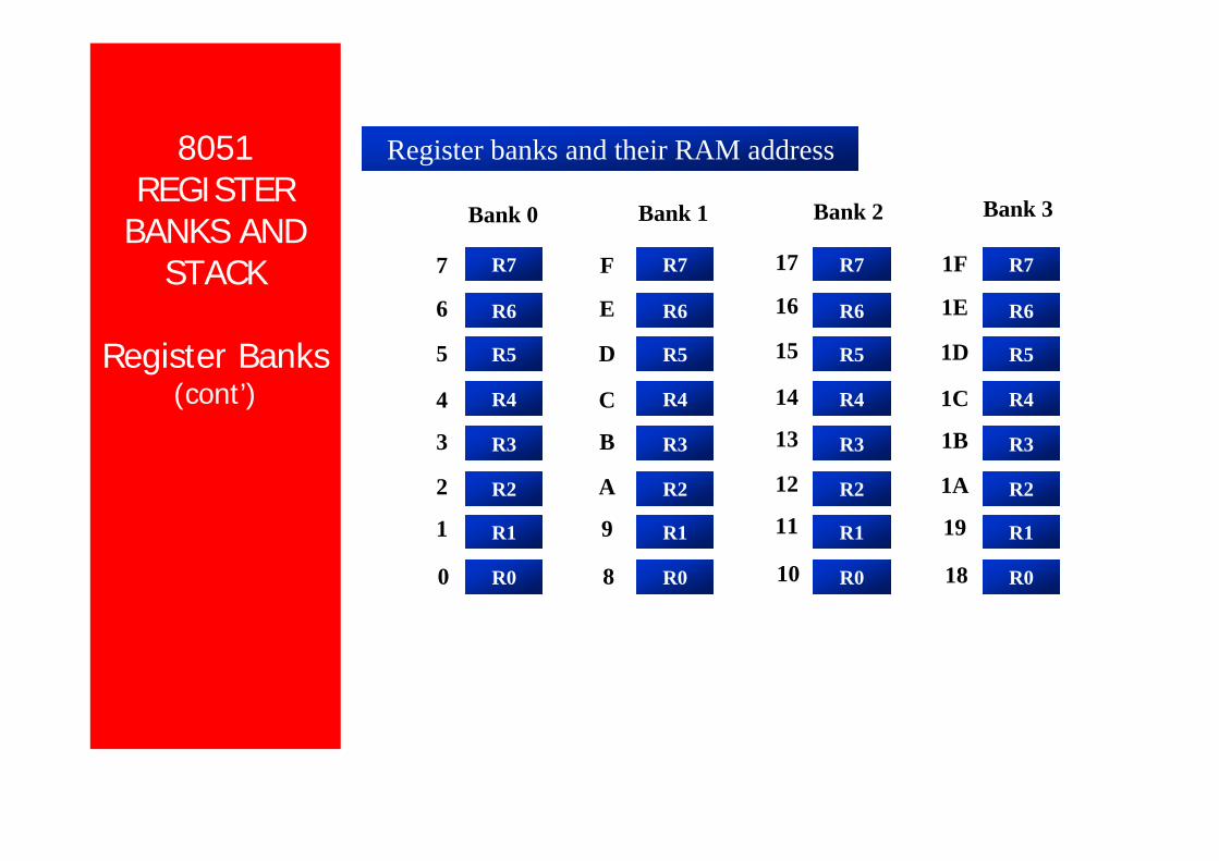
Register Banks
These 32 bytes are divided into 4banks of registers in which each bankhas 8 registers, R0-R7
RAM location from 0 to 7 are set aside forbank 0 of R0-R7 where R0 is RAM location0, R1 is RAM location 1, R2 is RAMlocation 2, and so on, until memorylocation 7 which belongs to R7 of bank 0It is much easier to refer to these RAMlocations with names such as R0, R1, andso on, than by their memory locations
Register bank 0 is the default when8051 is powered up
8051 REGISTER
BANKS AND STACK
Register Banks (cont’)
R7
R6
R5
R4
R3
R2
R1
R0
Bank 0 Bank 1 Bank 2 Bank 3
7
6
5
4
3
2
0
1
F
E
D
C
B
A
8
9
1F
1E
1D
1C
1B
1A
18
19
17
16
15
14
13
12
10
11
R7
R6
R5
R4
R3
R2
R1
R0
R7
R6
R5
R4
R3
R2
R1
R0
R7
R6
R5
R4
R3
R2
R1
R0
Register banks and their RAM address
8051 REGISTER
BANKS AND STACK
Register Banks (cont’)
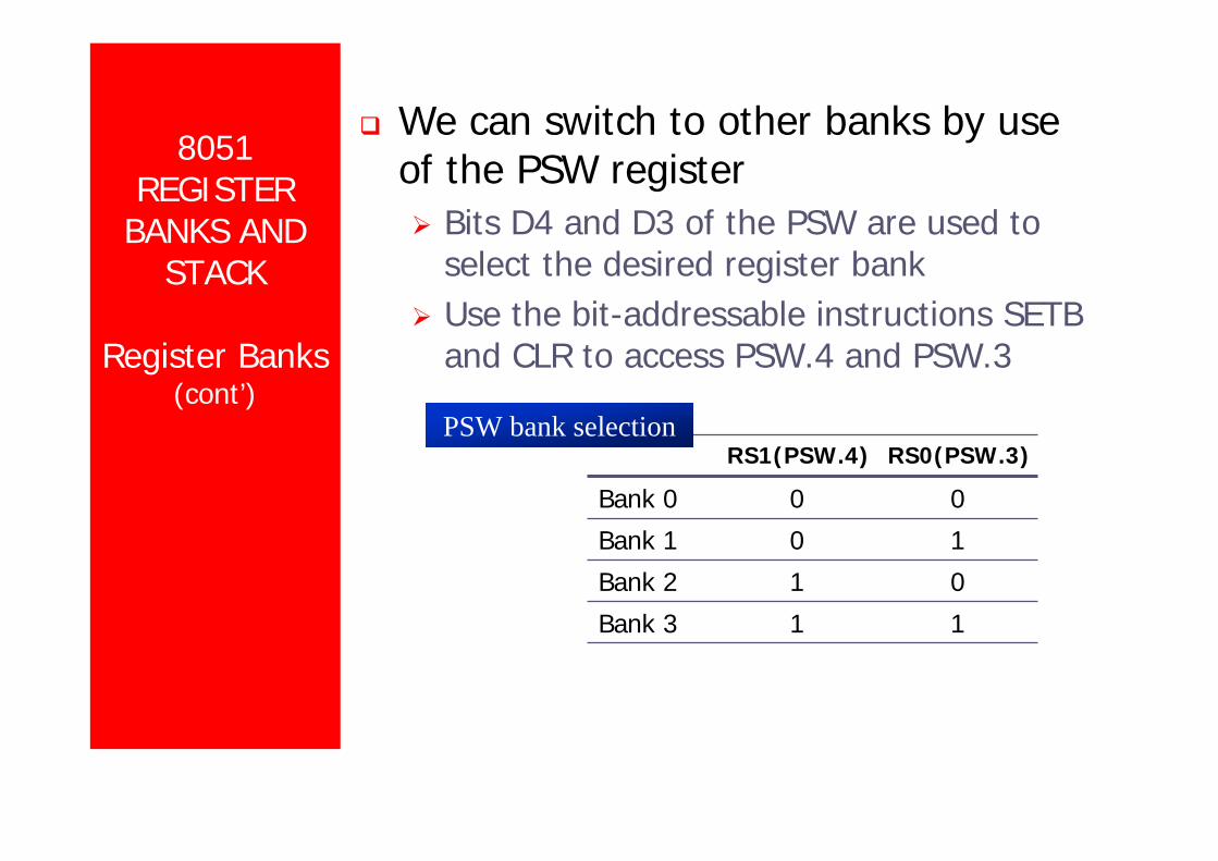
We can switch to other banks by useof the PSW register
Bits D4 and D3 of the PSW are used toselect the desired register bankUse the bit-addressable instructions SETBand CLR to access PSW.4 and PSW.3
11Bank 3
01Bank 2
10Bank 1
00Bank 0
RS0(PSW.3)RS1(PSW.4)PSW bank selection
8051 REGISTER
BANKS AND STACK
Register Banks (cont’)
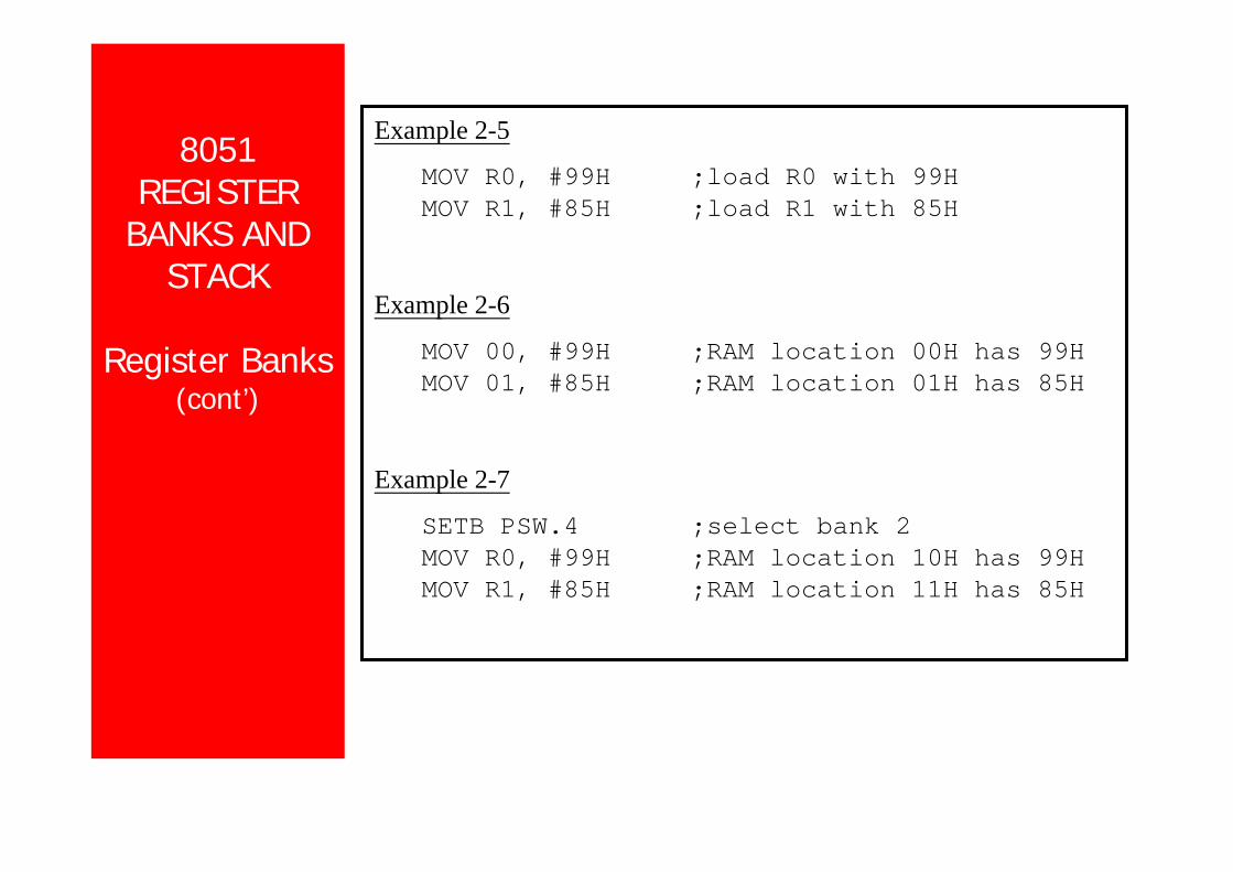
Example 2-5
MOV R0, #99H ;load R0 with 99HMOV R1, #85H ;load R1 with 85H
Example 2-6
MOV 00, #99H ;RAM location 00H has 99HMOV 01, #85H ;RAM location 01H has 85H
Example 2-7
SETB PSW.4 ;select bank 2MOV R0, #99H ;RAM location 10H has 99HMOV R1, #85H ;RAM location 11H has 85H
8051 REGISTER
BANKS AND STACK
Stack
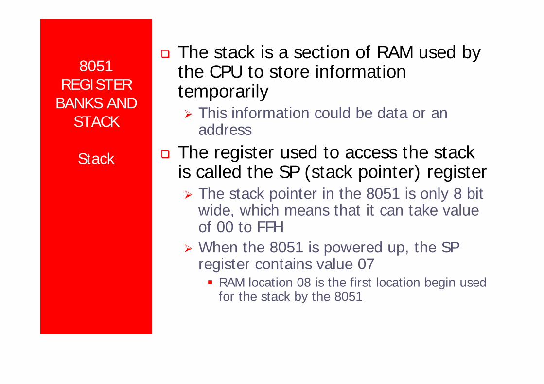
The stack is a section of RAM used bythe CPU to store informationtemporarily
This information could be data or anaddress
The register used to access the stackis called the SP (stack pointer) register
The stack pointer in the 8051 is only 8 bitwide, which means that it can take valueof 00 to FFHWhen the 8051 is powered up, the SPregister contains value 07
RAM location 08 is the first location begin usedfor the stack by the 8051
8051 REGISTER
BANKS AND STACK
Stack(cont’)
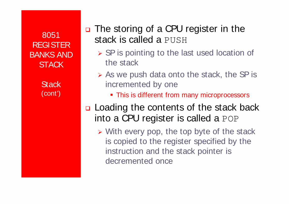
The storing of a CPU register in thestack is called a PUSH
SP is pointing to the last used location ofthe stackAs we push data onto the stack, the SP isincremented by one
This is different from many microprocessors
Loading the contents of the stack backinto a CPU register is called a POP
With every pop, the top byte of the stackis copied to the register specified by theinstruction and the stack pointer isdecremented once
8051 REGISTER
BANKS AND STACK
Pushing onto Stack
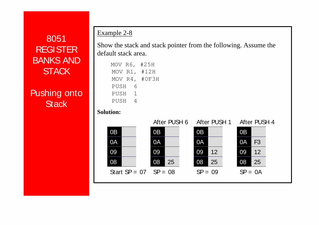
Example 2-8
Show the stack and stack pointer from the following. Assume the default stack area.
MOV R6, #25HMOV R1, #12HMOV R4, #0F3HPUSH 6PUSH 1PUSH 4
Solution:
25
12
F3
After PUSH 4
SP = 0A
08
09
0A
0B
SP = 09SP = 08Start SP = 07
2508250808
12090909
0A0A0A
0B0B0B
After PUSH 1After PUSH 6
8051 REGISTER
BANKS AND STACK
Popping From Stack
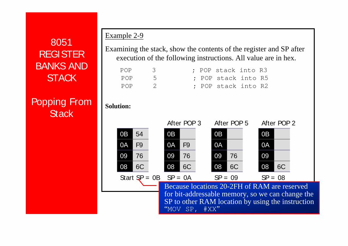
Example 2-9
Examining the stack, show the contents of the register and SP after execution of the following instructions. All value are in hex.POP 3 ; POP stack into R3POP 5 ; POP stack into R5POP 2 ; POP stack into R2
Solution:
6C
After POP 2
SP = 08
08
09
0A
0B
SP = 09SP = 0AStart SP = 0B
6C086C086C08
760976097609
0AF90AF90A
0B0B540B
After POP 5After POP 3
Because locations 20-2FH of RAM are reserved for bit-addressable memory, so we can change the SP to other RAM location by using the instruction “MOV SP, #XX”