EE410 vs. Advanced CMOS Structures - Stanford …web.stanford.edu/class/ee410/AdvCMOS.pdfEE410 vs....
12
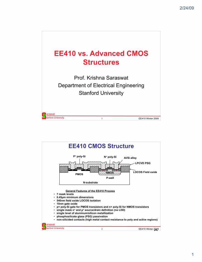
2/24/09 1 1 tanford University araswat EE410 Winter 2009 EE410 vs. Advanced CMOS Structures Prof. Krishna Saraswat Department of Electrical Engineering Stanford University 2 tanford University araswat EE410 Winter 2009 2 EE410 CMOS Structure Al/Si alloy P + poly-Si N + poly-Si LOCOS Field oxide LPCVD PSG General Features of the EE410 Process • 7 mask levels • 0.45µm minimum dimensions • 540nm field oxide LOCOS isolation • 10nm gate oxide • p+ poly-Si gate for PMOS transistors and n+ poly-Si for NMOS transistors • single mask n + and p + source/drain definition (no LDD) • single level of aluminum/silicon metallization • phosphosilicate glass (PSG) passivation • non-silicided contacts (high metal contact resistance to poly and active regions) N-substrate NMOS PMOS P-well P + P + N + N +
Transcript of EE410 vs. Advanced CMOS Structures - Stanford …web.stanford.edu/class/ee410/AdvCMOS.pdfEE410 vs....
2/24/09
1
1 tanford University araswat
EE410 Winter 2009
EE410 vs. Advanced CMOS Structures
Prof. Krishna Saraswat Department of Electrical Engineering
Stanford University
2 tanford University araswat
EE410 Winter 2009
2
EE410 CMOS Structure
Al/Si alloy P+ poly-Si N+ poly-Si
LOCOS Field oxide
LPCVD PSG
General Features of the EE410 Process • 7 mask levels • 0.45µm minimum dimensions • 540nm field oxide LOCOS isolation • 10nm gate oxide • p+ poly-Si gate for PMOS transistors and n+ poly-Si for NMOS transistors • single mask n+ and p+ source/drain definition (no LDD) • single level of aluminum/silicon metallization • phosphosilicate glass (PSG) passivation • non-silicided contacts (high metal contact resistance to poly and active regions)
N-substrate
NMOS PMOS P-well
P+ P+ N+ N+
2/24/09
2
3 tanford University araswat
EE410 Winter 2009
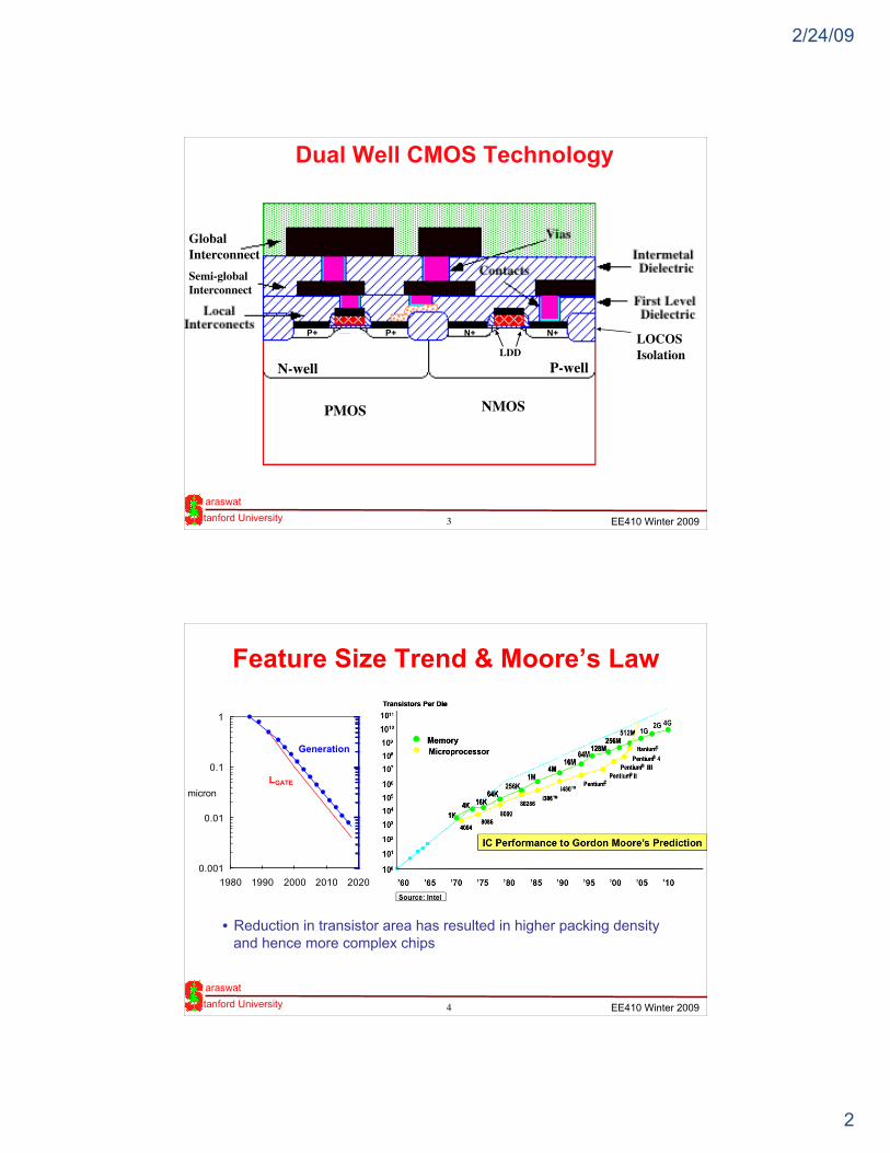
Dual Well CMOS Technology
PMOS NMOS
P-well N-well
P+ P+ N+ N+
Semi-global Interconnect
Global Interconnect
LDD LOCOS Isolation
4 tanford University araswat
EE410 Winter 2009
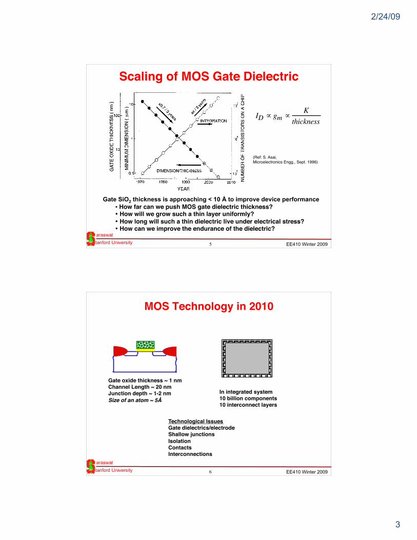
Feature Size Trend & Moore’s Law
0.001
0.01
0.1
1
1980 1990 2000 2010 2020
micron
Generation
LGATE
• Reduction in transistor area has resulted in higher packing density and hence more complex chips
2/24/09
3
5 tanford University araswat
EE410 Winter 2009
Scaling of MOS Gate Dielectric
(Ref: S. Asai, Microelectronics Engg., Sept. 1996)
Gate SiO2 thickness is approaching < 10 Å to improve device performance • How far can we push MOS gate dielectric thickness? • How will we grow such a thin layer uniformly? • How long will such a thin dielectric live under electrical stress? • How can we improve the endurance of the dielectric?
ID ∝ gm ∝K
thickness
6 tanford University araswat
EE410 Winter 2009
MOS Technology in 2010
In integrated system 10 billion components 10 interconnect layers
Technological Issues Gate dielectrics/electrode Shallow junctions Isolation Contacts Interconnections
Gate oxide thickness ~ 1 nm Channel Length ~ 20 nm Junction depth ~ 1-2 nm Size of an atom ~ 5Å
2/24/09
4
7 tanford University araswat
EE410 Winter 2009
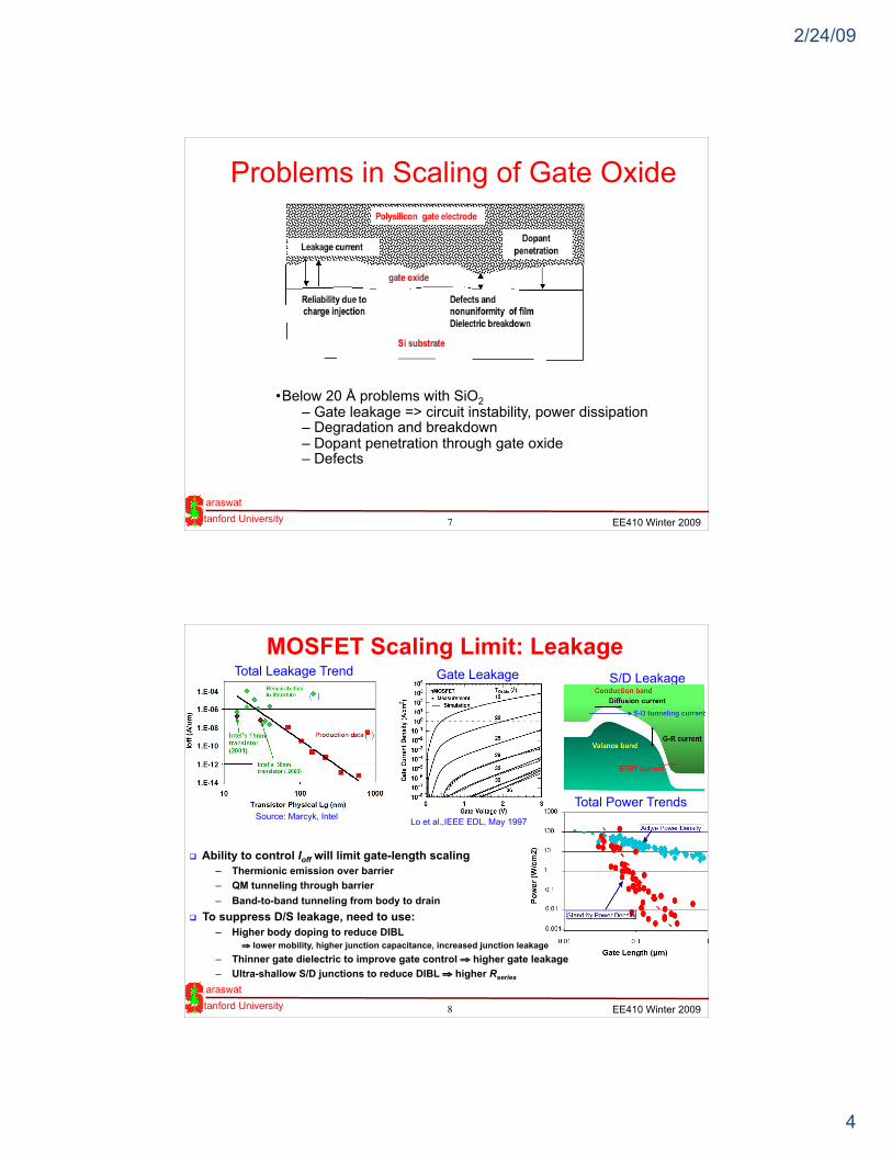
• Below 20 Å problems with SiO2 – Gate leakage => circuit instability, power dissipation – Degradation and breakdown – Dopant penetration through gate oxide – Defects
Problems in Scaling of Gate Oxide
8 tanford University araswat
EE410 Winter 2009
MOSFET Scaling Limit: Leakage
Lo et al.,IEEE EDL, May 1997.
Gate Leakage S/D Leakage
Source: Marcyk, Intel
Total Leakage Trend
Total Power Trends
Ability to control Ioff will limit gate-length scaling – Thermionic emission over barrier – QM tunneling through barrier – Band-to-band tunneling from body to drain
To suppress D/S leakage, need to use: – Higher body doping to reduce DIBL
⇒ lower mobility, higher junction capacitance, increased junction leakage – Thinner gate dielectric to improve gate control ⇒ higher gate leakage – Ultra-shallow S/D junctions to reduce DIBL ⇒ higher Rseries
2/24/09
5
9 tanford University araswat
EE410 Winter 2009
K ≈ 20
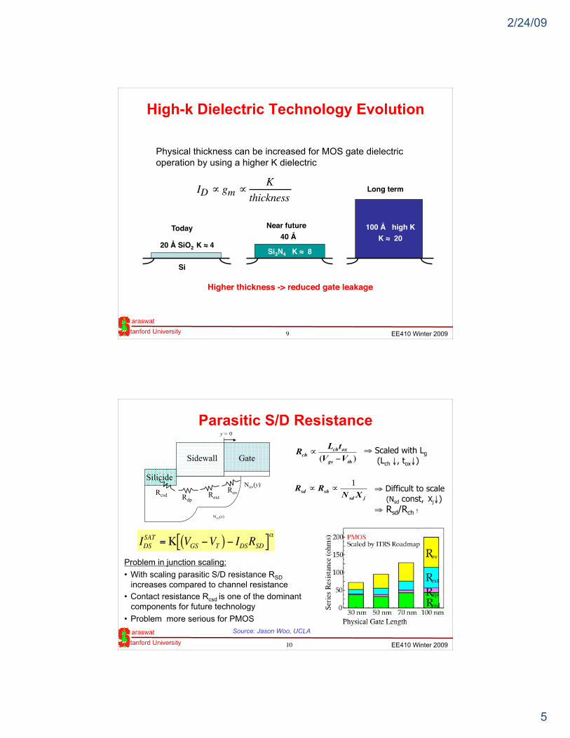
Physical thickness can be increased for MOS gate dielectric operation by using a higher K dielectric
Si3N4 K ≈ 8
40 Å Today Near future
Long term
20 Å SiO2 K ≈ 4
ID ∝ gm ∝K
thickness
100 Å high K
Si
Higher thickness -> reduced gate leakage
High-k Dielectric Technology Evolution
10 tanford University araswat
EE410 Winter 2009
Source: Jason Woo, UCLA
Problem in junction scaling: • With scaling parasitic S/D resistance RSD
increases compared to channel resistance • Contact resistance Rcsd is one of the dominant
components for future technology • Problem more serious for PMOS
€
IDSSAT =Κ VGS −VT( ) − IDSRSD[ ]α
)( thgs
oxchch VV
tLR−
∝ ⇒ Scaled with Lg (Lch ↓, tox↓)
jsdshsd XNRR 1
∝∝
Parasitic S/D Resistance
Rcsd Rdp Rext Rov
y = 0
Gate Sidewall
Silicide
Next(x)
Nov(y) ⇒ Difficult to scale (Nsd const, Xj↓) ⇒ Rsd/Rch ↑
2/24/09
6
11 tanford University araswat
EE410 Winter 2009
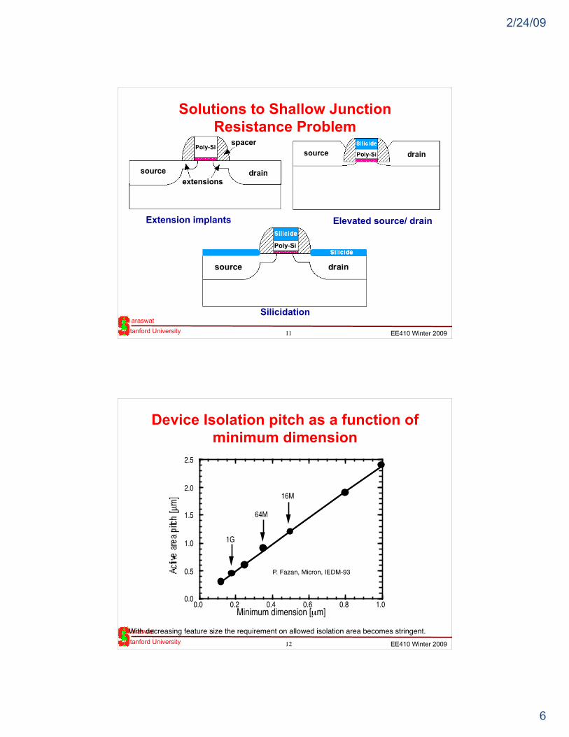
Solutions to Shallow Junction Resistance Problem
Extension implants Elevated source/ drain
Silicidation
12 tanford University araswat
EE410 Winter 2009
Device Isolation pitch as a function of minimum dimension
0.0 0.2 0.4 0.6 0.8 1.0Minimum dimension [µm]
0.0
0.5
1.0
1.5
2.0
2.5
16M
64M
1G
P. Fazan, Micron, IEDM-93
With decreasing feature size the requirement on allowed isolation area becomes stringent.
2/24/09
7
13 tanford University araswat
EE410 Winter 2009
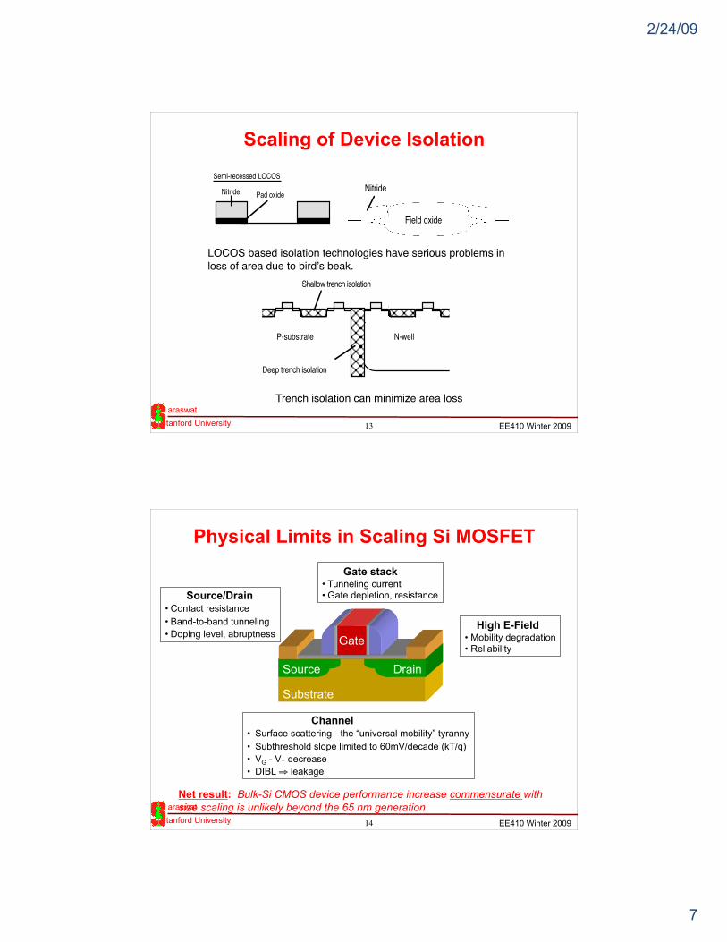
Scaling of Device Isolation
NitridePad oxide
Fully recessed LOCOS
Nitride Pad oxide
Semi-recessed LOCOSNitride
Field oxide
After field oxidation
After field oxidation
LOCOS based isolation technologies have serious problems in loss of area due to birdʼs beak.
Deep trench isolation
N-wellP-substrate
Shallow trench isolation
Trench isolation can minimize area loss
14 tanford University araswat
EE410 Winter 2009
Physical Limits in Scaling Si MOSFET
Substrate
Gate
Source Drain
Gate stack • Tunneling current • Gate depletion, resistance Source/Drain
• Contact resistance • Band-to-band tunneling • Doping level, abruptness
Channel • Surface scattering - the “universal mobility” tyranny • Subthreshold slope limited to 60mV/decade (kT/q) • VG - VT decrease • DIBL ⇒ leakage
Net result: Bulk-Si CMOS device performance increase commensurate with size scaling is unlikely beyond the 65 nm generation
High E-Field • Mobility degradation • Reliability
te
2/24/09
8
15 tanford University araswat
EE410 Winter 2009
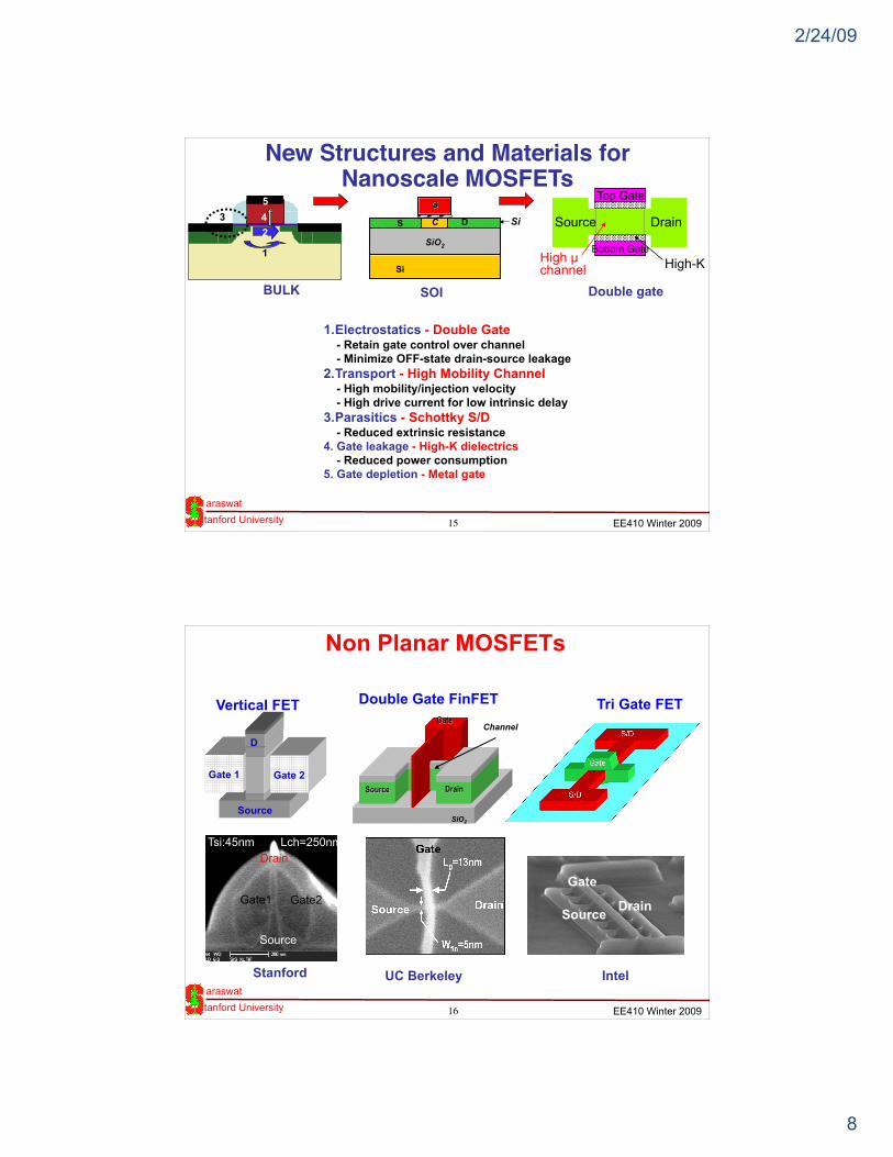
New Structures and Materials for Nanoscale MOSFETs
1. Electrostatics - Double Gate - Retain gate control over channel - Minimize OFF-state drain-source leakage 2. Transport - High Mobility Channel - High mobility/injection velocity - High drive current for low intrinsic delay 3. Parasitics - Schottky S/D - Reduced extrinsic resistance 4. Gate leakage - High-K dielectrics - Reduced power consumption 5. Gate depletion - Metal gate
1
2 3
GG
Si
S D Si
SiO2
C
BULK SOI Double gate
Bottom Gate
Top Gate
Source Drain
High µ channel High-K
4 5
16 tanford University araswat
EE410 Winter 2009
UC Berkeley
Gate
Source Drain
Intel
Tri Gate FET
SiO2
Channel
Double Gate FinFET Vertical FET
Stanford
Source
Gate 1 Gate 2
D
Tsi:45nm Lch=250nm
Gate1
Source
Drain
Gate2
Non Planar MOSFETs
2/24/09
9
17 tanford University araswat
EE410 Winter 2009
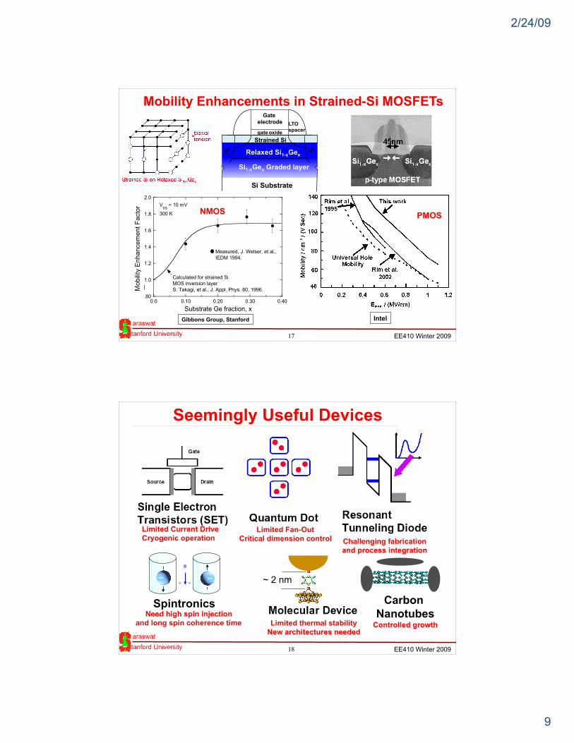
0.80
1.0
1.2
1.4
1.6
1.8
2.0
0.0 0.10 0.20 0.30 0.40
Mobility enhancement ratio
Substrate Ge fraction, x
VDS
= 10 mV
300 K
Measured, J. Welser, et al.,
IEDM 1994.
Calculated for strained Si
MOS inversion layer
S. Takagi, et al., J. Appl. Phys. 80, 1996.Mob
ility
Enh
ance
men
t Fac
tor
NMOS
Mobility Enhancements in Strained-Si MOSFETs
Intel
PMOS
Gibbons Group, Stanford
Strained Si gate oxide
Si Substrate
Relaxed Si1-xGex
n + p o l y LTO spacer
n + n + Si1-xGex Graded layer
Gate electrode
18 tanford University araswat
EE410 Winter 2009
B
+ =
Spintronics
Seemingly Useful Devices
Limited Current Drive Cryogenic operation
Limited Fan-Out Critical dimension control
Need high spin injection and long spin coherence time Limited thermal stability
New architectures needed
~ 2 nm
Challenging fabrication and process integration
Carbon Nanotubes
Controlled growth
2/24/09
10
19 tanford University araswat
EE410 Winter 2009
Cu (bulk)
Surface Scattering
Grain Boundary
Scattering
Combined
22nm
Node
32nm
Node
2.5X
bit rate B∝A/l2 l
A Old New (scaled)
Scaled wire with lower A and longer l has higher R,C and L and thus reduced bandwidth, higher delay and higher power dissipation
Limits of Interconnect
20 tanford University araswat
EE410 Winter 2009
Current Interconnect Technologies
Copper 6
Copper 1
TungstenLocal Interconnect
Copper 3
Copper 5
Copper 4
Copper 2
Current Al technology (Courtesy of Motorola)
Current Cu/low-K technology (Courtesy of IBM)
Reduced resistivity and dielectric constant results in improvement in performance.
2/24/09
11
21 tanford University araswat
EE410 Winter 2009
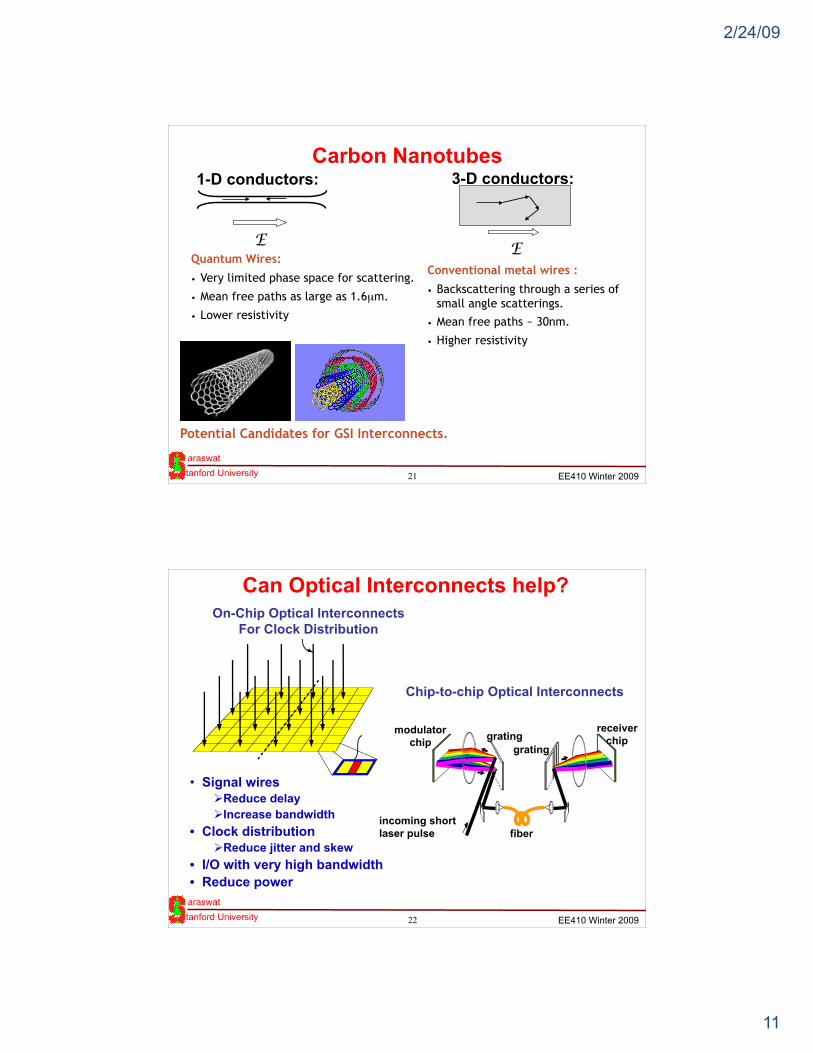
E E
1-D conductors: 3-D conductors:
Quantum Wires:
• Very limited phase space for scattering.
• Mean free paths as large as 1.6µm.
• Lower resistivity
Conventional metal wires :
• Backscattering through a series of small angle scatterings.
• Mean free paths ~ 30nm.
• Higher resistivity
Potential Candidates for GSI Interconnects.
Carbon Nanotubes
22 tanford University araswat
EE410 Winter 2009
Chip-to-chip Optical Interconnects
• Signal wires Reduce delay Increase bandwidth
• Clock distribution Reduce jitter and skew
• I/O with very high bandwidth • Reduce power
40Tb/s Optical I/O1024 x OC-768100Tb/s On-ChipBisection BWPMM64 Tiles64b Processor+ 4MB DRAMOn-Chip Optical Interconnects
For Clock Distribution
Can Optical Interconnects help?
incoming short laser pulse
grating grating
fiber
receiver chip
modulator chip
2/24/09
12
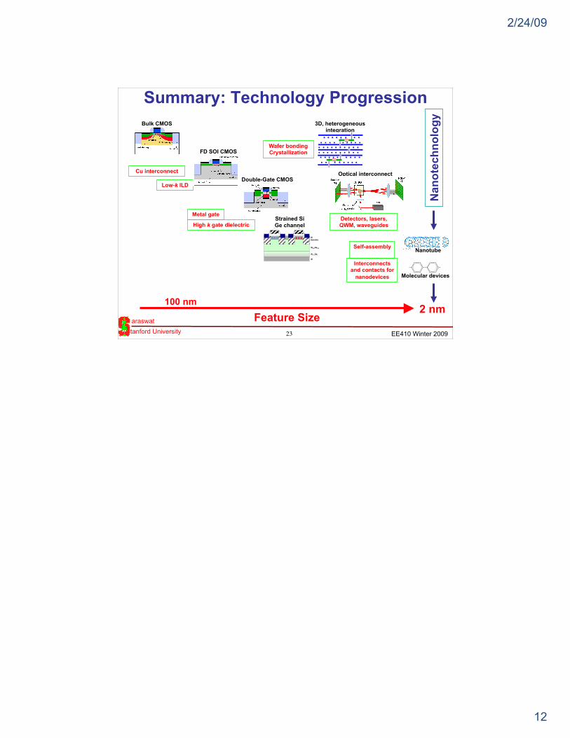
23 tanford University araswat
EE410 Winter 2009
Feature Size
Summary: Technology Progression Bulk CMOS
Si0.8Ge0.2
Si
Si(tensile)
Si1-xGex
Strained Si Ge channel High k gate dielectric
Self-assembly
Metal gate
Wafer bonding Crystallization
3D, heterogeneous integration
100 nm 2 nm
Cu interconnect
Low-k ILD
Nan
otec
hnol
ogy
Interconnects and contacts for
nanodevices
Double-Gate CMOS
FD SOI CMOS
Optical interconnect
Molecular devices
Nanotube
Detectors, lasers, QWM, waveguides


![Introduction20Plasma... · Web viewCrystalline and poly-crystalline Ge-on-Si has many applications in the fields of complementary metal oxide semiconductor (CMOS) electronics [],](https://static.fdocuments.net/doc/165x107/5ae72ea67f8b9a87048eea6e/introduction-20plasmaweb-viewcrystalline-and-poly-crystalline-ge-on-si-has-many.jpg)