EE141 VLSI Test Principles and Architectures Ch. 8 - Memory Testing & BIST - P. 1 1 Chapter 8 Memory...
90
EE141 1 Test Principles and Architectures Ch. 8 - Memory Testing & BIST - P. 1 Chapter 8 Chapter 8 emory Testing and Built-In Self-Te emory Testing and Built-In Self-Te
-
Upload
fay-hamilton -
Category
Documents
-
view
265 -
download
4
Transcript of EE141 VLSI Test Principles and Architectures Ch. 8 - Memory Testing & BIST - P. 1 1 Chapter 8 Memory...

EE1411
VLSI Test Principles and Architectures Ch. 8 - Memory Testing & BIST - P. 1
Chapter 8Chapter 8
Memory Testing and Built-In Self-TestMemory Testing and Built-In Self-Test

EE1412
VLSI Test Principles and Architectures Ch. 8 - Memory Testing & BIST - P. 2
What is this chapter about?What is this chapter about?
Basic concepts of memory testing and BIST
Memory fault models and test algorithms Memory fault simulation and test
algorithm generation RAMSES: fault simulator TAGS: test algorithm generator
Memory BIST BRAINS: BIST generator

EE1413
VLSI Test Principles and Architectures Ch. 8 - Memory Testing & BIST - P. 3
Typical RAM Production FlowTypical RAM Production Flow
WaferWafer Full Probe Test
Marking
Final Test ShippingQA Sample TestVisual Inspection
Burn-In (BI)Post-BI Test
Laser Repair Packaging
Pre-BI Test

EE1414
VLSI Test Principles and Architectures Ch. 8 - Memory Testing & BIST - P. 4
Off-Line Testing of RAMOff-Line Testing of RAM
Parametric Test: DC & AC Reliability Screening
Long-cycle testing Burn-in: static & dynamic BI
Functional Test Device characterization
– Failure analysis Fault modeling
– Simple but effective (accurate & realistic?) Test algorithm generation
– Small number of test patterns (data backgrounds)– High fault coverage– Short test time

EE1415
VLSI Test Principles and Architectures Ch. 8 - Memory Testing & BIST - P. 5
DRAM Functional ModelDRAM Functional Model

EE1416
VLSI Test Principles and Architectures Ch. 8 - Memory Testing & BIST - P. 6
DRAM Functional Model ExampleDRAM Functional Model Example

EE1417
VLSI Test Principles and Architectures Ch. 8 - Memory Testing & BIST - P. 7
Functional Fault ModelsFunctional Fault Models Classical fault models are not sufficient to
represent all important failure modes in RAM. Sequential ATPG is not possible for RAM. Functional fault models are commonly used
for memories: They define functional behavior of faulty
memories.
New fault models are being proposed to cover new defects and failures in modern memories: New process technologies New devices

EE1418
VLSI Test Principles and Architectures Ch. 8 - Memory Testing & BIST - P. 8
Static RAM Fault Models: SAF/TFStatic RAM Fault Models: SAF/TF Stuck-At Fault (SAF)
Cell (line) SA0 or SA1– A stuck-at fault (SAF) occurs when the value of a cell or
line is always 0 (a stuck-at-0 fault) or always 1 (a stuck-at-1 fault).
– A test that detects all SAFs guarantees that from each cell, a 0 and a 1 must be read.
Transition Fault (TF) Cell fails to transit from 0 to 1 or 1 to 0 in specified
time period.– A cell has a transition fault (TF) if it fails to transit from 0
to 1 (a </0> TF) or from 1 to 0 (a </1> TF).

EE1419
VLSI Test Principles and Architectures Ch. 8 - Memory Testing & BIST - P. 9
Static RAM Fault Models: AFStatic RAM Fault Models: AF Address-Decoder Fault (AF)
An address decoder fault (AF) is a functional fault in the address decoder that results in one of four kinds of abnormal behavior:
– Given a certain address, no cell will be accessed
– A certain cell is never accessed by any address– Given a certain address, multiple cells are
accessed– A certain cell can be accessed by multiple
addresses

EE14110
VLSI Test Principles and Architectures Ch. 8 - Memory Testing & BIST - P. 10
Static RAM Fault Models: SOFStatic RAM Fault Models: SOF Stuck-Open Fault (SOF)
A stuck-open fault (SOF) occurs when the cell cannot be accessed due to, e.g., a broken word line.
A read to this cell will produce the previously read value.

EE14111
VLSI Test Principles and Architectures Ch. 8 - Memory Testing & BIST - P. 11
RAM Fault Models: CFRAM Fault Models: CF Coupling Fault (CF)
A coupling fault (CF) between two cells occurs when the logic value of a cell is influenced by the content of, or operation on, another cell.
State Coupling Fault (CFst)– Coupled (victim) cell is forced to 0 or 1 if coupling
(aggressor) cell is in given state.
Inversion Coupling Fault (CFin)– Transition in coupling cell complements (inverts) coupled
cell.
Idempotent Coupling Fault (CFid)– Coupled cell is forced to 0 or 1 if coupling cell transits
from 0 to 1 or 1 to 0.

EE14112
VLSI Test Principles and Architectures Ch. 8 - Memory Testing & BIST - P. 12
Intra-Word & Inter-Word CFsIntra-Word & Inter-Word CFs

EE14113
VLSI Test Principles and Architectures Ch. 8 - Memory Testing & BIST - P. 13
RAM Fault Models: DFRAM Fault Models: DF Disturb Fault (DF)
Victim cell forced to 0 or 1 if we (successively) read or write aggressor cell (may be the same cell):
– Hammer test
Read Disturb Fault (RDF)– There is a read disturb fault (RDF) if the cell
value will flip when being read (successively).

EE14114
VLSI Test Principles and Architectures Ch. 8 - Memory Testing & BIST - P. 14
RAM Fault Models: DRFRAM Fault Models: DRF Data Retention Fault (DRF)
DRAM– Refresh Fault
– Leakage Fault
SRAM– Leakage Fault
Static Data Losses---defective pull-up

EE14115
VLSI Test Principles and Architectures Ch. 8 - Memory Testing & BIST - P. 15
Test Time Complexity Test Time Complexity (100MHz)(100MHz)
Size N 10N NlogN N1.5 N2
1M 0.01s 0.1s 0.2s 11s 3h
16M 0.16s 1.6s 3.9s 11m 33d
64M 0.66s 6.6s 17s 1.5h 1.43y
256M 2.62s 26s 1.23m 12h 23y
1G 10.5s 1.8m 5.3m 4d 366y
4G 42s 7m 22.4m 32d 57c
16G 2.8m 28m 1.6h 255d 915c

EE14116
VLSI Test Principles and Architectures Ch. 8 - Memory Testing & BIST - P. 16
RAM Test AlgorithmRAM Test Algorithm A test algorithm (or simply test) is a finite
sequence of test elements: A test element contains a number of memory
operations (access commands)– Data pattern (background) specified for the Read and
Write operation– Address (sequence) specified for the Read and Write
operations
A march test algorithm is a finite sequence of march elements: A march element is specified by an address order
and a finite number of Read/Write operations

EE14117
VLSI Test Principles and Architectures Ch. 8 - Memory Testing & BIST - P. 17
March Test NotationMarch Test Notation : address sequence is in the ascending
order : address changes in the descending order : address sequence is either or r: the Read operation
Reading an expected 0 from a cell (r0); reading an expected 1 from a cell (r1)
w: the Write operation Writing a 0 into a cell (w0); writing a 1 into a cell (w1)
Example (MATS+): )}0,1();1,0();0({ wrwrw

EE14118
VLSI Test Principles and Architectures Ch. 8 - Memory Testing & BIST - P. 18
Classical Test Algorithms: MSCANClassical Test Algorithms: MSCAN Zero-One Algorithm [Breuer & Friedman 1976]
Also known as MSCAN SAF is detected if the address decoder is correct
(not all AFs are covered):– Theorem: A test detects all AFs if it contains the march
elements (ra,…,wb) and (rb,…,wa), and the memory is initialized to the proper value before each march element
Solid background (pattern) Complexity is 4N
)}1();1();0();0({ rwrw

EE14119
VLSI Test Principles and Architectures Ch. 8 - Memory Testing & BIST - P. 19
Classical Test Algorithms: CheckerboardClassical Test Algorithms: Checkerboard Checkerboard Algorithm
Zero-one algorithm with checkerboard pattern Complexity is 4N Must create true physical checkerboard, not
logical checkerboard For SAF, DRF, shorts between cells, and half of
the TFs– Not good for AFs, and some CFs cannot be detected
1 0 10 1 01 0 1

EE14120
VLSI Test Principles and Architectures Ch. 8 - Memory Testing & BIST - P. 20
Classical Test Algorithms: GALPATClassical Test Algorithms: GALPAT Galloping Pattern (GALPAT)
Complexity is 4N**2─only for characterization A strong test for most faults: all AFs, TFs, CFs, and
SAFs are detected and located
1. Write background 0;
2. For BC = 0 to N-1
{ Complement BC;
For OC = 0 to N-1, OC != BC;
{ Read BC; Read OC; }
Complement BC; }
3. Write background 1;
4. Repeat Step 2;
BC

EE14121
VLSI Test Principles and Architectures Ch. 8 - Memory Testing & BIST - P. 21
Classical Test Algorithms: WALPATClassical Test Algorithms: WALPAT Walking Pattern (WALPAT)
Similar to GALPAT, except that BC is read only after all others are read.
Complexity is 2N**2.
BC

EE14122
VLSI Test Principles and Architectures Ch. 8 - Memory Testing & BIST - P. 22
Classical Test Algorithms: SlidingClassical Test Algorithms: Sliding Sliding (Galloping) Row/Column/Diagonal
Based on GALPAT, but instead of shifting a 1 through the memory, a complete diagonal of 1s is shifted:
– The whole memory is read after each shift Detects all faults as GALPAT, except for some CFs Complexity is 4N**1.5. 1
1
1
1
1

EE14123
VLSI Test Principles and Architectures Ch. 8 - Memory Testing & BIST - P. 23
Classical Test Algorithms: ButterflyClassical Test Algorithms: Butterfly Butterfly Algorithm
Complexity is 5NlogN All SAFs and some AFs are detected
1. Write background 0;
2. For BC = 0 to N-1
{ Complement BC; dist = 1;
While dist <= mdist /* mdist < 0.5 col/row length */
{ Read cell @ dist north from BC;
Read cell @ dist east from BC;
Read cell @ dist south from BC;
Read cell @ dist west from BC;
Read BC; dist *= 2; }
Complement BC; }
3. Write background 1; repeat Step 2;
6
1
9 4 5,10 2 7
3
8

EE14124
VLSI Test Principles and Architectures Ch. 8 - Memory Testing & BIST - P. 24
Classical Test Algorithms: MOVIClassical Test Algorithms: MOVI Moving Inversion (MOVI) Algorithm
For functional and AC parametric test– Functional (13N): for AF, SAF, TF, and most CF
– Parametric (12NlogN): for Read access time 2 successive Reads @ 2 different addresses with different
data for all 2-address sequences differing in 1 bit
Repeat T2~T5 for each address bit
GALPAT---all 2-address sequences
)}0,0,1();1,1,0();0,0,1();1,1,0();0({ rwrrwrrwrrwrw

EE14125
VLSI Test Principles and Architectures Ch. 8 - Memory Testing & BIST - P. 25
Classical Test Algorithms: SDClassical Test Algorithms: SD Surround Disturb Algorithm
Examine how the cells in a row are affected when complementary data are written into adjacent cells of neighboring rows.
Designed on the premise that DRAM cells are most susceptible to interference from their nearest neighbors (eliminates global sensitivity checks).
1. For each cell[p,q] /* row p and column q */ { Write 0 in cell[p,q-1]; Write 0 in cell[p,q]; Write 0 in cell[p,q+1]; Write 1 in cell[p-1,q]; Read 0 from cell[p,q+1]; Write 1 in cell[p+1,q]; Read 0 from cell[p,q-1]; Read 0 from cell[p,q]; }2. Repeat Step 1 with complementary data;
1
0 0 0
1

EE14126
VLSI Test Principles and Architectures Ch. 8 - Memory Testing & BIST - P. 26
Simple March TestsSimple March Tests Zero-One (MSCAN) Modified Algorithmic Test Sequence (MATS)
OR-type address decoder fault
AND-type address decoder fault
MATS+ For both OR- & AND-type AFs and SAFs The suggested test for unlinked SAFs
)}1();1,0();0({ rwrw
)}0();0,1();1({ rwrw
)}0,1();1,0();0({ wrwrw

EE14127
VLSI Test Principles and Architectures Ch. 8 - Memory Testing & BIST - P. 27
March Tests: Marching-1/0 March Tests: Marching-1/0 Marching-1/0
Marching-1: begins by writing a background of 0s, then read and write back complement values (and read again to verify) for all cells (from cell 0 to n-1, and then from cell n-1 to 0), in 7N time
Marching-0: follows exactly the same pattern, with the data reversed
For AF, SAF, and TF (but only part of the CFs) It is a complete test, i.e., all faults that should be
detected are covered It however is a redundant test, because only the
first three march elements are necessary
)}1,1,0();0,0,1();1(
);0,0,1();1,1,0();0({
rwrrwrw
rwrrwrw

EE14128
VLSI Test Principles and Architectures Ch. 8 - Memory Testing & BIST - P. 28
March Tests: MATS++March Tests: MATS++ MATS++
Also for AF, SAF, and TF
Optimized marching-1/0 scheme—complete and
irredundant
Similar to MATS+, but allow for the coverage of TFs
The suggested test for unlinked SAFs & TFs
)}0,0,1();1,0();0({ rwrwrw

EE14129
VLSI Test Principles and Architectures Ch. 8 - Memory Testing & BIST - P. 29
March Tests: March X/CMarch Tests: March X/C March X
Called March X because the test has been used without being published
For AF, SAF, TF, & CFin
March C For AF, SAF, TF, & all CFs, but semi-optimal
(redundant)
)}0();0,1();1,0();0({ rwrwrw
)}0();0,1();1,0();0(
);0,1();1,0();0({
rwrwrr
wrwrw

EE14130
VLSI Test Principles and Architectures Ch. 8 - Memory Testing & BIST - P. 30
March Tests: March C-March Tests: March C- March C-
Remove the redundancy in March C Also for AF, SAF, TF, & all CFs Optimal (irredundant)
)}0();0,1();1,0();0,1();1,0();0({ rwrwrwrwrw
Extended March C- Covers SOF in addition to the above faults
)}0();0,1();1,0();0,1();1,1,0();0({ rwrwrwrrwrw

EE14131
VLSI Test Principles and Architectures Ch. 8 - Memory Testing & BIST - P. 31
Fault Detection SummaryFault Detection Summary
EE14132
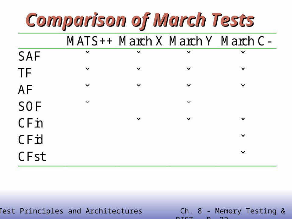
VLSI Test Principles and Architectures Ch. 8 - Memory Testing & BIST - P. 32
Comparison of March TestsComparison of March Tests MATS++ March X March Y March C- SAF ˇ ˇ ˇ ˇ TF ˇ ˇ ˇ ˇ AF ˇ ˇ ˇ ˇ SOF ˇ ˇ CFin ˇ ˇ ˇ CFid ˇ CFst ˇ

EE14133
VLSI Test Principles and Architectures Ch. 8 - Memory Testing & BIST - P. 33
Word-Oriented MemoryWord-Oriented Memory A word-oriented memory has
Read/Write operations that access the memory cell array by a word instead of a bit.
Word-oriented memories can be tested by applying a bit-oriented test algorithm repeatedly with a set of different data backgrounds: The repeating procedure multiplies the
testing time

EE14134
VLSI Test Principles and Architectures Ch. 8 - Memory Testing & BIST - P. 34
Testing Word-Oriented RAMTesting Word-Oriented RAM Background bit is replaced by background
word MATS++:
Conventional method is to use logm+1 different backgrounds for m-bit words Called standard backgrounds m=8: 00000000, 01010101, 00110011, and
00001111 Apply the test algorithm logm+1=4 times, so
complexity is 4*6N/8=3N
)},,();,();({ rawarbwbrawa
Note: b is the complement of a

EE14135
VLSI Test Principles and Architectures Ch. 8 - Memory Testing & BIST - P. 35
Cocktail-March AlgorithmsCocktail-March Algorithms Motivation:
Repeating the same algorithm for all logm+1 backgrounds is redundant so far as intra-word coupling faults are concerned
Different algorithms target different faults.
Approaches:1. Use multiple backgrounds in a single
algorithm run2. Merge and forge different algorithms and
backgrounds into a single algorithm
Good for word-oriented memoriesRef: Wu et al., IEEE TCAD, 04/02

EE14136
VLSI Test Principles and Architectures Ch. 8 - Memory Testing & BIST - P. 36
March-CWMarch-CW Algorithm:
March C- for solid background (0000) Then a 5N March for each of other standard
backgrounds (0101, 0011):
Results: Complexity is (10+5logm)N, where m is word length
and N is word count Test time is reduced by 39% if m=4, as compared
with extended March C- Improvement increases as m increases
)},,,,({ rawarbwbwa
Ref: Wu et al., IEEE TCAD, 04/02

EE14137
VLSI Test Principles and Architectures Ch. 8 - Memory Testing & BIST - P. 37
Multi-Port Memory Fault ModelsMulti-Port Memory Fault Models Cell Faults:
Single cell faults: SAF, TF, RDF Two-cell coupling faults
– Inversion coupling fault (CFin) – State coupling fault (CFst)– Idempotent coupling fault (CFid)
Port Faults: Stuck-open fault (SOF) Address decoder fault (AF) Multi-port fault (MPF)

EE14138
VLSI Test Principles and Architectures Ch. 8 - Memory Testing & BIST - P. 38
2-Port RAM Topology2-Port RAM Topology
WL
Interport BL short
Interport WL shortWL
WL
WL
WL
WL
WL
WL
BL BLBL BL
BL BL BL BL
A
B
A
B
A
A
A
A
B
B
B
A
B
B
B
A
1
2
3

EE14139
VLSI Test Principles and Architectures Ch. 8 - Memory Testing & BIST - P. 39
Inter-Port Word-Line ShortInter-Port Word-Line Short
* Functional test complexity: O(N3)
Faulty
Cell 1
Fault-Free
Cell 2
Address 3
Address 2
Cell 3
Address 1 Cell 1Address 1
Port B
Port A
Cell 2Address 2

EE14140
VLSI Test Principles and Architectures Ch. 8 - Memory Testing & BIST - P. 40
Inter-Port Bit-Line ShortInter-Port Bit-Line Short
Port A
Fault-Free
Port BCell
Address Cell
Address
Faulty
Address Address
Cell Cell
Address
Address
Cell
Cell
* Functional test complexity: O(N2)

EE14141
VLSI Test Principles and Architectures Ch. 8 - Memory Testing & BIST - P. 41
Why Memory Fault Simulation?Why Memory Fault Simulation? Fault coverage evaluation can be done
efficiently, especially when the number of fault models is large.
In addition to bit-oriented memories, word-oriented memories can be simulated easily even with multiple backgrounds.
Test algorithm design and optimization can be done in a much easier way.
Detection of a test algorithm on unexpected faults can be discovered.
Fault dictionary can be constructed for easy diagnosis.

EE14142
VLSI Test Principles and Architectures Ch. 8 - Memory Testing & BIST - P. 42
Sequential Memory Fault SimulationSequential Memory Fault Simulation Complexity is N**3 for 2-cell CF
For each fault /* N**2 for 2-cell CF */
Inject fault;
For each test element /* N for March */
{
Apply test element;
Report error output;
}

EE14143
VLSI Test Principles and Architectures Ch. 8 - Memory Testing & BIST - P. 43
Parallel Fault SimulationParallel Fault Simulation RAMSES [Wu, Huang, & Wu, DFT99 & IEEE TCAD 4/02]
Each fault model has a fault descriptor
# S/1AGR := w0SPT := @ /* Single-cell fault */VTM := r0RCV := w1
# CFst <0;s/1>AGR := v0SPT := * /* All other cells are suspects */VTM := r0RCV := w1

EE14144
VLSI Test Principles and Architectures Ch. 8 - Memory Testing & BIST - P. 44
RAMSESRAMSES Complexity is N**2
For each test operation
{
If op is AGR then mark victim cells;
If op is RCV then release victim cells;
If op is VTM then report error;
}

EE14145
VLSI Test Principles and Architectures Ch. 8 - Memory Testing & BIST - P. 45
RAMSES AlgorithmRAMSES Algorithm

EE14146
VLSI Test Principles and Architectures Ch. 8 - Memory Testing & BIST - P. 46
RAMSES Example for CFin<RAMSES Example for CFin<;;>>

EE14147
VLSI Test Principles and Architectures Ch. 8 - Memory Testing & BIST - P. 47
Coverage of March TestsCoverage of March TestsMATS++ March X March Y March C-
SAF 1 1 1 1TF 1 1 1 1AF 1 1 1 1SOF 1 .002 1 .002CFin .75 1 1 1CFid .375 .5 .5 1CFst .5 .625 .625 1
☞ Extended March C- has 100% coverage of SOF

EE14148
VLSI Test Principles and Architectures Ch. 8 - Memory Testing & BIST - P. 48
Test Algorithm Generation GoalsTest Algorithm Generation Goals Given a set of target fault models, generate a
test with 100% fault coverage Given a set of target fault models and a test
length constraint, generate a test with the highest fault coverage
Priority setting for fault models Test length/test time can be reduced
Diagnostic test generation Need longer test to distinguish faults

EE14149
VLSI Test Principles and Architectures Ch. 8 - Memory Testing & BIST - P. 49
Test Algorithm Generation by Simulation (TAGS)Test Algorithm Generation by Simulation (TAGS)
March template abstraction:
↑(w0); ↑(r0,w1); ↓(r1,w0,r0)
↑(w) ↑(r,w); ↓(r,w,r)
(w)(rw)(rwr)

EE14150
VLSI Test Principles and Architectures Ch. 8 - Memory Testing & BIST - P. 50
Template SetTemplate Set Exhaustive generation: complexity is very
high, e.g., 6.7 million templates when N = 9 Heuristics should be developed to select
useful templates
T(1N) (w)
T(2N) (ww) (w)(r)(wr)(w)(w)
T(3N) (www) (ww)(w) (w)(ww)
(wwr) (wrw) (wr)(w) ….(w)(rw)

EE14151
VLSI Test Principles and Architectures Ch. 8 - Memory Testing & BIST - P. 51
TAGS ProcedureTAGS Procedure1. Initialize test length as 1N, T(1N) = {(w)};2. Increase test length by 1N: apply generation
options;3. Apply filter options;4. Assign address orders and data
backgrounds;5. Fault simulation using RAMSES;6. Drop ineffective tests;7. Repeat 2-6 using the new template set until
constraints met;

EE14152
VLSI Test Principles and Architectures Ch. 8 - Memory Testing & BIST - P. 52
Template Generation/FilteringTemplate Generation/Filtering Generation heuristics:
(r) insertion (…r), (r…) expansion (w) insertion (…w), (w…) expansion
Filtering heuristics: Consecutive read: (…rr…) Repeated read: (r)(r) Tailing single write: …(w)

EE14153
VLSI Test Principles and Architectures Ch. 8 - Memory Testing & BIST - P. 53
TAGS Example (1/2)TAGS Example (1/2) Target fault models (SAF, TF, AF, SOF, Cfin,
Cfid, CFst), time constraints ∞:

EE14154
VLSI Test Principles and Architectures Ch. 8 - Memory Testing & BIST - P. 54
TAGS Example (2/2)TAGS Example (2/2)

EE14155
VLSI Test Principles and Architectures Ch. 8 - Memory Testing & BIST - P. 55
RAMSES Simulation ResultsRAMSES Simulation Results

EE14156
VLSI Test Principles and Architectures Ch. 8 - Memory Testing & BIST - P. 56
FC Spectrum for 6FC Spectrum for 6NN Tests Tests

EE14157
VLSI Test Principles and Architectures Ch. 8 - Memory Testing & BIST - P. 57
Word-Oriented TAGSWord-Oriented TAGS1. Construct bit-oriented test algorithms2. Generate initial Cocktail-March: Assign each data background
to the test in Step 1─a cascade of multiple March algorithms3. Optimize the Cocktail-March (!P1) /* non-solid backgrounds */4. Optimize the Cocktail-March (P1) /* solid background */

EE14158
VLSI Test Principles and Architectures Ch. 8 - Memory Testing & BIST - P. 58
3. Cocktail March Optimization (!P3. Cocktail March Optimization (!P11))For each non-solid data background P (P != P1)
a) Generate a new Cocktail–March test by replacing the March algorithm having P as its background with a shorter one from the set of algorithms generated in Step 1.
b) Run RAMSES for the new Cocktail–March.
c) Repeat 3(a) and 3(b) until the FC drops and cannot be recovered by any other test algorithm of the same length.
d) Store the test algorithm candidates used in the previous step.

EE14159
VLSI Test Principles and Architectures Ch. 8 - Memory Testing & BIST - P. 59
4. Cocktail March Optimization (P4. Cocktail March Optimization (P11))a) Generate a new Cocktail–March test by
replacing the March algorithm having P1 as its background with a shorter one from the test set generated in Step 1. Repeat with every test candidate for other backgrounds.
b) Run RAMSES for the new Cocktail–March.
c) Repeat 4(a) and 4(b) for all candidate test algorithms from 3(d) until the FC drops and cannot be recovered by any other test algorithm of the same length or by selecting other candidates.

EE14160
VLSI Test Principles and Architectures Ch. 8 - Memory Testing & BIST - P. 60
Cocktail March Example (m=8)Cocktail March Example (m=8)
Ref: Wu et al., IEEE TCAD, 4/02

EE14161
VLSI Test Principles and Architectures Ch. 8 - Memory Testing & BIST - P. 61
What Can BIST do?What Can BIST do? What are the functional faults to be covered?
Static and dynamic Operation modes
What are the defects to be covered? Opens, shorts, timing parameters, voltages, currents, etc.
Can it support fault location and redundancy repair? Can it support BI? Can it support on-chip redundancy analysis and
repair? Does it allow characterization test as well as mass
production test? Can it really replace ATE (and laser repair machine)?
Programmability, speed, timing accuracy, threshold range, parallelism, etc.

EE14162
VLSI Test Principles and Architectures Ch. 8 - Memory Testing & BIST - P. 62
Typical RAM BIST ApproachesTypical RAM BIST Approaches Methodology
Processor-based BIST– Programmable
Hardwired BIST– Fast– Compact
Hybrid Interface
Serial (scan, 1149.1) Parallel (embedded controller; hierarchical)
Patterns (address sequence) March & March-like Pseudorandom Others

EE14163
VLSI Test Principles and Architectures Ch. 8 - Memory Testing & BIST - P. 63
Typical RAM BIST ArchitectureTypical RAM BIST Architecture
RAMT
est C
ollar (M
UX
)
BIST Module
Controller
Comparator
Pattern
Generator
Go/No-Go
RAM Controller

EE14164
VLSI Test Principles and Architectures Ch. 8 - Memory Testing & BIST - P. 64
EDO DRAM BIST ExampleEDO DRAM BIST Example

EE14165
VLSI Test Principles and Architectures Ch. 8 - Memory Testing & BIST - P. 65
DRAM Page-Mode Read-Write CycleDRAM Page-Mode Read-Write Cycle

EE14166
VLSI Test Principles and Architectures Ch. 8 - Memory Testing & BIST - P. 66
BIST ArchitectureBIST Architecture

EE14167
VLSI Test Principles and Architectures Ch. 8 - Memory Testing & BIST - P. 67
BIST External I/OBIST External I/O MBS (Memory BIST Selection): controller test collar
(normal/test mode selection) MBC (Memory BIST Control): Controller input MCK (Memory BIST Clock) MBR (Memory BIST Reset) MSI (Memory BIST Scan In): for test commands and
scan test inputs MSO (Memory BIST Scan Out): for diagnostic data
and scan test outputs MBO (Memory BIST Output): error indicator MRD (Memory BIST Output Ready): BIST completion
flag

EE14168
VLSI Test Principles and Architectures Ch. 8 - Memory Testing & BIST - P. 68
BIST I/O SummaryBIST I/O Summary

EE14169
VLSI Test Principles and Architectures Ch. 8 - Memory Testing & BIST - P. 69
Controller and SequencerController and Sequencer Controller
Microprogram Hardwired Shared CPU core IEEE 1149.1 TAP PLD
Sequencer (Pattern Generator) Counter LFSR LUT PLD

EE14170
VLSI Test Principles and Architectures Ch. 8 - Memory Testing & BIST - P. 70
ControllerController

EE14171
VLSI Test Principles and Architectures Ch. 8 - Memory Testing & BIST - P. 71
SequencerSequencer
Combination Logic #0
Row Address Counter
Column AddressCounter
State
Combination Logic #1
eDRAMcontrolsignal
MCKMCK
Flags
eDRAMBIST
Controller
D Q
D Q
D Q
D Q
D Q
D Q
D Q
D Q
Control Counter
Comparator

EE14172
VLSI Test Principles and Architectures Ch. 8 - Memory Testing & BIST - P. 72
Sequencer StatesSequencer StatesDisable
BIST_EN=lowSEQ_EN=low
All outputs andflags are high-z
Reset/InitiateBIST_EN=highSEQ_EN=highAll outputs andflags seted toknown state
NON_EDOA
WD
Done &Change
Command
CBR Refresh
NON_EDOB
RDWD'EDO_ROW
EDO_COL0
WD
EDO_ROW
EDO_COL2
RDWD'RD'
EDO_ROW
EDO_COL1
RDWD'
SelfRefresh
Idle& WaitBIST_EN=highSEQ_EN=low
All outputs andflags are inprecharged
state

EE14173
VLSI Test Principles and Architectures Ch. 8 - Memory Testing & BIST - P. 73
BIST Test ModesBIST Test Modes
1. Scan-Test Mode
2. RAM-BIST Mode
1.Functional faults
2.Timing faults (setup/hold times, rise/fall times,
etc.)
3.Data retention faults
3. RAM-Diagnosis Mode
4. RAM-BI Mode

EE14174
VLSI Test Principles and Architectures Ch. 8 - Memory Testing & BIST - P. 74
BIST Controller CommandsBIST Controller CommandsBit 4
Addressing orderBit 3
Data typeBit 2, Bit 1, Bit 0
Operations1: (increasing) 1: d = DB 000: EOT (End of test)0: (decreasing) 0: d = ~DB 001: Rd (READ Cycle)
010: Wd (Early WRITE Cycle)011: RdW~d (READ-WRITE) Cycle
EDO-PAGE-MODE100: Wd (Early WRITE Cycle101: RdW~d (READ-WRITE) Cycle110: RdW~dR~d (READ Early WRITE Cycle)111: Refresh

EE14175
VLSI Test Principles and Architectures Ch. 8 - Memory Testing & BIST - P. 75
BIST Control SequenceBIST Control Sequence

EE14176
VLSI Test Principles and Architectures Ch. 8 - Memory Testing & BIST - P. 76
RAM BIST CompilerRAM BIST Compiler Use of RAM cores is increasing
SRAM, DRAM, flash RAM Multiple cores
RAM BIST compiler is the trend BRAINS (BIST for RAM in Seconds)
Proposed BIST Architecture Memory Modeling Command Sequence Generation Configuration of the Proposed BIST

EE14177
VLSI Test Principles and Architectures Ch. 8 - Memory Testing & BIST - P. 77
BRAINS Output SpecificationBRAINS Output Specification
Synthesizable BIST design At-speed testing
Programmable March algorithms
Optional diagnosis support– BISD
Activation sequence Test bench Synthesis script

EE14178
VLSI Test Principles and Architectures Ch. 8 - Memory Testing & BIST - P. 78
BRAINS Inputs and OutputsBRAINS Inputs and Outputs

EE14179
VLSI Test Principles and Architectures Ch. 8 - Memory Testing & BIST - P. 79
General RAM BIST ArchitectureGeneral RAM BIST Architecture
Controller
Memory
MBS
Test C
ollar
Sequencer
Comparator
MBCMBRMSI
MSO
MRD
MBO
MCK
NormalAccess
Controls
Address
D
Q
Programmable Memory BIST
TPG

EE14181
VLSI Test Principles and Architectures Ch. 8 - Memory Testing & BIST - P. 81
Function of the TPGFunction of the TPG
The test pattern generator (TPG) translates high-level memory commands to memory input signals.
Four parameters to model a memory’s I/Os: Type: input, output, and in/out Width Latency: number of clock cycles the TPG generates the
physical signal after it receives a command from the sequencer
Packet_length: number of different signal values packed within a single clock cycle
BISTController Sequencer TPG RAM

EE14182
VLSI Test Principles and Architectures Ch. 8 - Memory Testing & BIST - P. 82
Architecture of the TPGArchitecture of the TPG

EE14183
VLSI Test Principles and Architectures Ch. 8 - Memory Testing & BIST - P. 83
Multiple RAM CoresMultiple RAM Cores Controller and sequencer can be shared
controller
Test pattern generator
Test pattern generator
sequencer
Ram Core ARam Core A
Ram Core BRam Core B
Ram Core CRam Core CTest pattern generator
sequencer

EE14184
VLSI Test Principles and Architectures Ch. 8 - Memory Testing & BIST - P. 84
Sharing Controller & SequencerSharing Controller & Sequencer

EE14185
VLSI Test Principles and Architectures Ch. 8 - Memory Testing & BIST - P. 85
Grouping and SchedulingGrouping and Scheduling

EE14186
VLSI Test Principles and Architectures Ch. 8 - Memory Testing & BIST - P. 86
BRAINS BIST ArchitectureBRAINS BIST Architecture
MBS MSI MBO MRD MSO MBC MBR MCK
Sequencer Sequencer Sequencer
TPGTPGTPGTPGTPGTPG
RAM RAM RAM RAM
MemoryBIST
External Tester
Controller
RAMRAM
Source: ATS’01

EE14187
VLSI Test Principles and Architectures Ch. 8 - Memory Testing & BIST - P. 87
BRAINS GUIBRAINS GUI

EE14188
VLSI Test Principles and Architectures Ch. 8 - Memory Testing & BIST - P. 88
Supported MemoriesSupported Memories The Built-In Memory List
DRAM– EDO DRAM– SDRAM– DDR SDRAM
SRAM– Single-Port Synchronous SRAM– Single-Port Asynchronous SRAM– Two-Port Synchronous Register File– Dual-Port Synchronous SRAM– Micron ZBT SRAM
BRAINS can support new memory architectures easily

EE14189
VLSI Test Principles and Architectures Ch. 8 - Memory Testing & BIST - P. 89
ExamplesExamples

EE14190
VLSI Test Principles and Architectures Ch. 8 - Memory Testing & BIST - P. 90
Area OverheadArea Overhead

EE14191
VLSI Test Principles and Architectures Ch. 8 - Memory Testing & BIST - P. 91
Concluding RemarksConcluding Remarks BIST is considered the best solution for
testing embedded memories: Low cost Effective and efficient
Further improvement can be expected to extend the scope of RAM BIST: Timing/delay faults and disturb faults BISD and BISR CAM BIST and flash BIST BIST/BISD/BISR compiler Wafer-level BI and test
– Known good die