EE 330 Lecture 31
42
EE 330 Lecture 31 Thyristors – wrap up Amplifier Biasing (a precursor) Amplifier Characterization Amplifier Characterization • Amplifier parameters • Two-port amplifier models • Dependent Sources
Transcript of EE 330 Lecture 31

EE 330
Lecture 31
Thyristors – wrap up
Amplifier Biasing (a precursor)
Amplifier Characterization
Amplifier Characterization
• Amplifier parameters
• Two-port amplifier models
• Dependent Sources

Exam 3 Friday April 13

Thyristor Types
• SCR
• Triac
• Bidirectional Phase-controlled thyristors (BCT)
• LASCR (Light activated SCR)
• Gate Turn-off thyristors (GTO)
• FET-controlled thyristors(FET-CTH)
• MOS Turn-off thyristors (MTO)
• MOS-controlled thyristors (MCT)
Some of the more major types:

Thyristor Applications
Thyristors are available for working at very low
current levels in electronic circuits to moderate
current levels such is in incandescent light
dimmers to very high current levels
ITRIAC from under 1mA to 10000A
Applications most prevalent for moderate to high
current thyristors

SCR, rated about 100 amperes, 1200 volts, 1/2 inch stud, photographed by C J
Cowie. Uploaded on 4 April 2006.

Thanks to Prof. Ajjarapu for providing the following slides:

From ABB Web Site
Diameter = 140mm

1988 Paper
Thanks to Prof. Ajjarapu for providing the following slides:
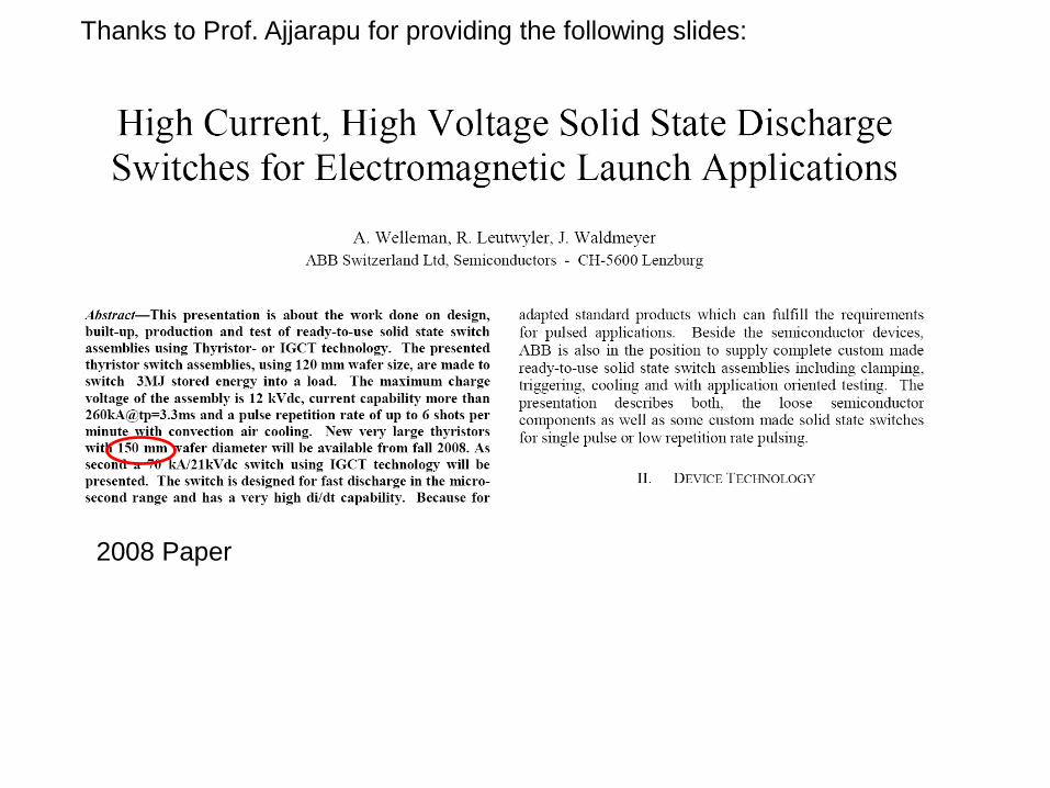
2008 Paper
Thanks to Prof. Ajjarapu for providing the following slides:

Thanks to Prof. Ajjarapu for providing the following slides:
Control Circuit
Thyristor

Stud- Mounted SCR110 Amp RMS Rating
Stud Anode
Cathode Lead
Gate Lead(White)
AuxiliaryCathode Lead (Red)Extends cathodepotential to thecontrol circuit.
Thanks to Prof. Ajjarapu for providing the following slides:

Cross-section of a BCT wafer showing the antiparallel arrangement of the A and Bcomponent thyristors. The arrows indicate the convention of forward blocking for A and B.
Thanks to Prof. Ajjarapu for providing the following slides:
Thyristor Valve - 12 Pulse Converter ( 6.5Kv, 1568 Amp, Water cooled)
Thanks to Prof. Ajjarapu for providing the following slides:

Thyristor Observations
Many different structures used to build thyristors
Range from low power devices to extremely high power devices
Often single-wafer solutions for high power applications
Usually formed by diffusions
Widely used throughout society but little visibility
Applications somewhat restricted

Thyristors
The good
SCRs
Triacs
The bad
Parasitic Device that can destroy integrated circuits

The Thyristor
S G D GSD
Consider a Bulk-CMOS Process
A bipolar device in CMOS Processes
If this parasitic SCR turns on, either circuit will latch up or destroy itself
Guard rings must be included to prevent latchup
Design rules generally include provisions for guard rings

Amplifier Biasing (precursor)
B
E
C
VCC
Vin
R1
Vout
VEE
Q1
• Voltage sources VEE and VCC used for biasing
• Not convenient to have multiple dc power supplies
• VOUTQ very sensitive to VEE
Biasing is used to obtain the desired operating point of a circuit
Ideally the biasing circuit should not distract significantly from the basic
operation of the circuit

Amplifier Biasing (precursor)
B
E
C
VCC
Vin
R1
Vout
VEE
Q1
Not convenient to have multiple dc power supplies
VOUTQ very sensitive to VEE
B
E
C
VCC=12V
Vin
R1=2K
Vout
Q1
RB=500K
C1=1uF
Compare the small-signal equivalent circuits of these two structures
Single power supply
Additional resistor and capacitor
Compare the small-signal voltage gain of these two structures
Will See this
is the Biasing
Circuit

Amplifier Biasing (precursor)
B
E
C
VCC
Vin
R1
Vout
VEE
Q1
B
E
C
VCC=12V
Vin
R1=2K
Vout
Q1
RB=500K
C1=1uF
Compare the small-signal equivalent circuits of these two structures
R1
VIN
VOUT
R1
VIN
VOUT
RB
Since Thevenin equivalent circuit in red circle is VIN, both circuits have same voltage gain
But the load placed on VIN is different
Method of characterizing the amplifiers is needed to assess impact of difference

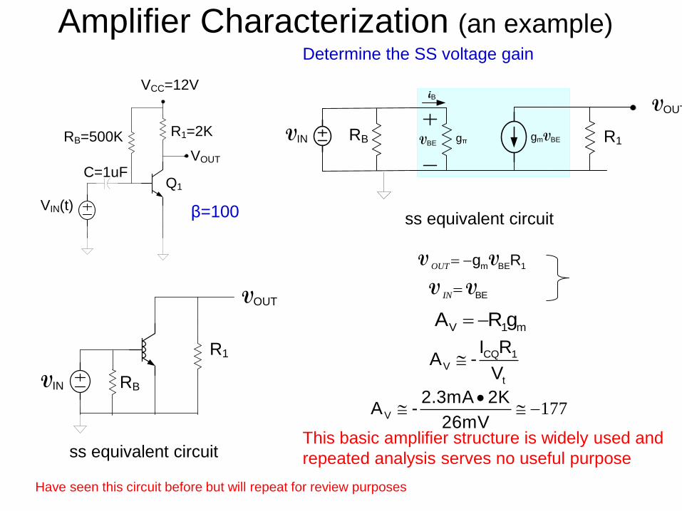
Amplifier Characterization (an example)
Determine VOUTQ, AV, RIN
B
E
C
VCC=12V
Vin
R1=2K
Vout
Q1
RB=500K
C1=1uF
Determine VOUT and VOUT(t) if VIN=.002sin(400t)
In the following slides we will analyze this circuit
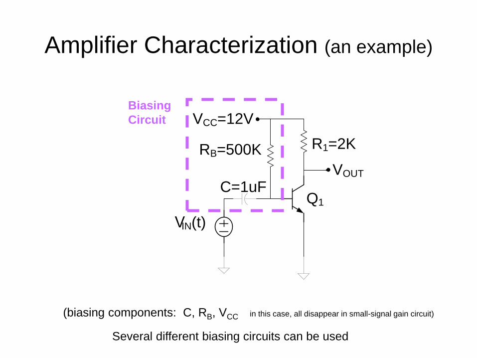
Amplifier Characterization (an example)
R1=2K
Q1
VOUT
VCC=12V
VIN(t)
RB=500K
C=1uF
Several different biasing circuits can be used
Biasing
Circuit
(biasing components: C, RB, VCC in this case, all disappear in small-signal gain circuit)

R1=2K
Q1
VOUT
VCC=12V
VIN(t)
RB=500K
C=1uF
Biasing
Circuit
Determine VOUTQ and the SS voltage gain, assume β=100
Amplifier Characterization (an example)

R1=2K
Q1
VOUT
VCC=12V
VIN(t)
RB=500K
C=1uF
Determine VOUTQ
β=100
R2=2K
Q1
VOUT
VCC=12V
RB1=500K
IB simplified
R2=2K VOUTQ
VCC=12V
RB1=500K
IB
0.6V
βIB
dc equivalent circuit
dc equivalent circuit
CQ BQ
12V-0.6VI = βI =100 2.3mA
500K
OUTQ CQ 1V = 12V-I R =12V - 2.3mA 2K 7.4V
Amplifier Characterization (an example)
R1=2K
Q1
VOUT
VCC=12V
VIN(t)
RB=500K
C=1uF
Determine the SS voltage gain
β=100
R1
VIN
VOUT
RB
ss equivalent circuit
Have seen this circuit before but will repeat for review purposes
R1
VOUT
VIN RB gmVBEVBE
iB
gπ
ss equivalent circuit
m BE 1g ROUT V V
BEINV V
V 1 mA R g
CQ 1V
t
I RA -
V
This basic amplifier structure is widely used and
repeated analysis serves no useful purpose
177V
2.3mA 2KA -
26mV
Amplifier Characterization (an example)

R1=2K
Q1
VOUT
VCC=12V
VIN(t)
RB=500K
C=1uF
Determine RIN
β=100
Amplifier Characterization (an example)
VIN
Linear One-Port
Facing Input
RIN
• Here RIN is defined to be the impedance facing VIN
• Here any load is assumed to be absorbed into the
one-port
• Later will consider how load is connected in
defining RIN

R1=2K
Q1
VOUT
VCC=12V
VIN(t)
RB=500K
C=1uF
Determine RIN
β=100
R1
VIN
VOUT
RB
ss equivalent circuit
INin
IN
R V
i
R1
VOUT
VIN RB gmVBEVBE
iB
gπ
RIN
iIN
//inR BR r
Usually RB>>rπ
/ /inR BR r r
CQin
t
IR
βV r
Amplifier Characterization (an example)

ExamplesDetermine VOUT and VOUT(t) if VIN=.002sin(400t)
B
E
C
VCC=12V
Vin
R1=2K
Vout
Q1
RB=500K
C1=1uF
OUT OUTQ V INV t V +A V
7.4 .35 sin(400 )OUTV - 0 V t
OUT V IN AV V
177 .002sin(400 ) 0.354sin(400 )OUT t t V

Two-Port Representation of Amplifiers
R1=2K
Q1
VOUT
VCC=12V
VIN(t)
RB=500K
C=1uFRL
R1
VIN
VOUT
RB
RL
R1
VOUT
VIN RB gmVBEVBE
iB
gπ RL
Two-Port Network
• Two-port model representation of amplifiers useful for insight into operation and analysis
• Internal components to the two-port can be quite complicated but equivalent two-port model
is quite simple

Two-port representation of amplifiers
y11 y22 V2
y21V1
y12V2V1
Amplifiers can be modeled as a two-port for small-signal operation
• Amplifier often unilateral (signal propagates in only one direction: wlog y12=0)
• One terminal is often common
y11y22 V2
y21V1
V1
In terms of y-parameters
Other parameter sets could be used

Two-port representation of amplifiers
RINV2
AVV1
V1
ROUT
• Thevenin equivalent output port often more standard
• RIN, AV, and ROUT often used to characterize the two-port of amplifiers
y11y22 V2
y21V1
V1
Unilateral amplifier in terms of “amplifier” parameters

Amplifier input impedance, output
impedance and gain are usually of interest
Example 1: Assume amplifier is unilateral
VIN
RS
Amplifier RL
VOUT
RIN V2
AVV1
V1
ROUT
VIN
RS
RL
VOUT
L INOUT V IN
L OUT S IN
R RV = A V
R +R R +R
OUT L INVAMP V
IN L OUT S IN
V R RA = = A
V R +R R +R
Can get gain without recondsidering details about components internal to the Amplifier !!!
Why?
Analysis more involved when not unilateral

Amplifier input impedance, output
impedance and gain are usually of interest
Example 2: Assume amplifiers are unilateral
Can get gain without recondsidering details about components internal to the Amplifier !!!
Why?
VIN
RS
Amplifier 1 Amplifier 2 Amplifier 3 RL
VOUT
RIN1 V21
AV1V11
V11
ROUT1
VIN
RS
RIN2 V22
AV2V12
V12
ROUT2
RIN3 V23
AV3V31
V13
ROUT3
RL
VOUT
IN3L IN2 IN1OUT V3 V2 V1 IN
L OUT3 OUT2 IN3 OUT1 IN2 S IN1
RR R RV = A A A V
R +R R +R R +R R +R
OUT IN3L IN2 IN1VAMP V3 V2 V1
IN L OUT3 OUT2 IN3 OUT1 IN2 S IN1
V RR R RA = = A A A
V R +R R +R R +R R +R
Analysis more involved when not unilateral

Two-port representation of amplifiers
y11y22 V2
y21V1
y12V2V1
• Amplifier usually unilateral (signal propagates in only one direction: wlog y12=0)
• One terminal is often common
• “Amplifier” parameters often used
y11y22 V2
y21V1
V1 V1 V2
I1 I2
RIN
ROUT
AVV1
Two Port (Thevenin)
V1 V2
I1 I2RIN ROUT
AVV1AVRV2
Two Port (Thevenin)
• Amplifier parameters can also be used if not unilateral
• One terminal is often common
y parameters Amplifier parameters
y parameters Amplifier parameters

Determination of small-signal model parameters:
In the past, we have determined small-signal model parameters from the
nonlinear port characteristics
2122
2111
,VVfI
,VVfI
QVVj
21iij
V
,VVfy
• Will now determine small-signal model parameters for two-port comprised
of linear networks
• Results are identical but latter approach is often much easier
y11y22 V2
y21V1
y12V2V1 V1 V2
I1 I2RIN ROUT
AVV1AVRV2
Two Port (Thevenin)
V1 V2
I1 I2RIN ROUT
AVV1AVRV2
Two Port (Thevenin)
y11A y22A
y12AV2A
y21AV1A
V1A V2A
i1Ai2A
y11B y22B
y12BV2B
y21BV1B
V1B V2B
i1Bi2B V2
i2
V1
i1
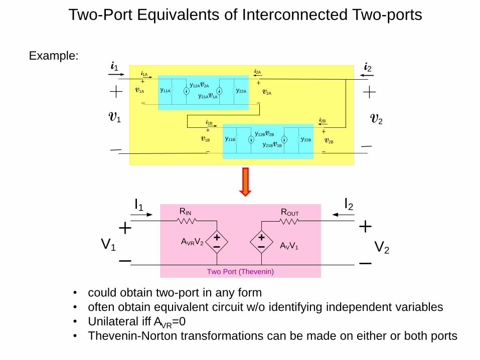
Two-Port Equivalents of Interconnected Two-ports
• could obtain two-port in any form
• often obtain equivalent circuit w/o identifying independent variables
• Unilateral iff AVR=0
• Thevenin-Norton transformations can be made on either or both ports
Example:

V1 V2
I1 I2RIN ROUT
AVV1AVRV2
Two Port (Thevenin)
y11A y22A
y12AV2A
y21AV1A
V1A V2A
i1Ai2A
R1
RB
V1B V2B
I1B I2B
g22B
g21BV2B g12BV1B
g11B
Two Port (Norton)
i1C
Linear Two Port
v1C
i2C
v2C
H-parameters
(Hybrid Parameters)
1 11 1 12 2C C C C Ch h V i v
2 21 1 22 2C C C C Ch h i i v
RXX
V1
i1
V2
i2
Two-Port Equivalents of Interconnected Two-ports
Example:

Determination of two-port model parameters
A method of obtaining Rin
Ro
V1
itest
v0 1A V V2
Rin
i2
Vtest
i1
vR 2A V
testin
test
R V
i
Terminate the output in a short-circuit
1 1 2
2 1 2
0 0
1
1
VR
V0
A
R R
A
R R
in in
i V + V
i V V
2 0V
(One method will be discussed here)y11A y22A
y12AV2A
y21AV1A
V1A V2A
i1Ai2A
R1
RB
V1B V2B
I1B I2B
g22B
g21BV2B g12BV1B
g11B
Two Port (Norton)
i1C
Linear Two Port
v1C
i2C
v2C
H-parameters
(Hybrid Parameters)
1 11 1 12 2C C C C Ch h V i v
2 21 1 22 2C C C C Ch h i i v
RXX
1
1
test
test
V V
i i

Determination of two-port model parameters
A method of obtaining AV0
Terminate the output in an open-circuit
out-testV0
test
A V
V
1 1 2
2 1 2
0 0
1
1
VR
V0
A
R R
A
R R
in in
i V V
i V V
2 0i
Ro
V1
v0 1A V V2
Rin
i2
Vtest
i1
vR 2A V Vout-test
y11A y22A
y12AV2A
y21AV1A
V1A V2A
i1Ai2A
R1
RB
V1B V2B
I1B I2B
g22B
g21BV2B g12BV1B
g11B
Two Port (Norton)
i1C
Linear Two Port
v1C
i2C
v2C
H-parameters
(Hybrid Parameters)
1 11 1 12 2C C C C Ch h V i v
2 21 1 22 2C C C C Ch h i i v
RXX
1
2
test
out-test
V V
V V

Determination of two-port model parameters
A method of obtaining R0
Terminate the input in a short-circuit
test0
test
R V
i
1 1 2
2 1 2
0 0
1
1
VR
V0
A
R R
A
R R
in in
i V V
i V V
1 0V
Ro
V1
v0 1A V V2
Rin
i2i1
vR 2A VVtest
itest
y11A y22A
y12AV2A
y21AV1A
V1A V2A
i1Ai2A
R1
RB
V1B V2B
I1B I2B
g22B
g21BV2B g12BV1B
g11B
Two Port (Norton)
i1C
Linear Two Port
v1C
i2C
v2C
H-parameters
(Hybrid Parameters)
1 11 1 12 2C C C C Ch h V i v
2 21 1 22 2C C C C Ch h i i v
RXX

Determination of two-port model parameters
A method of obtaining AVR
Ro
V1
i1
v0 1A VV2
Rin
i2
vR 2A VVtestVout-test
Terminate the input in an open-circuit
out-testVR
test
A V
V
1 1 2
2 1 2
0 0
1
1
VR
V0
A
R R
A
R R
in in
i V V
i V V
1 0i
y11A y22A
y12AV2A
y21AV1A
V1A V2A
i1Ai2A
R1
RB
V1B V2B
I1B I2B
g22B
g21BV2B g12BV1B
g11B
Two Port (Norton)
i1C
Linear Two Port
v1C
i2C
v2C
H-parameters
(Hybrid Parameters)
1 11 1 12 2C C C C Ch h V i v
2 21 1 22 2C C C C Ch h i i v
RXX
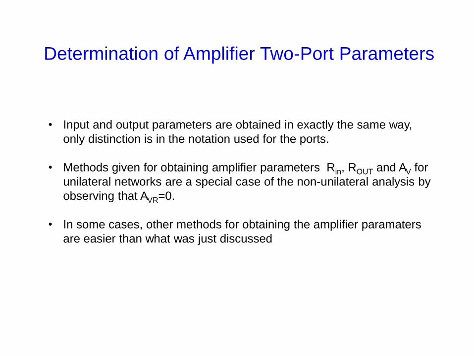
Determination of Amplifier Two-Port Parameters
• Input and output parameters are obtained in exactly the same way,
only distinction is in the notation used for the ports.
• Methods given for obtaining amplifier parameters Rin, ROUT and AV for
unilateral networks are a special case of the non-unilateral analysis by
observing that AVR=0.
• In some cases, other methods for obtaining the amplifier paramaters
are easier than what was just discussed

End of Lecture 31