eDM-COMB-KL6 · DATA MODUL provides the BIOS update tool, CPLD update tool, API test tool, ... The...
86
www.data-modul.com SPECIFICATION | SAFETY INSTRUCTIONS eDM-COMB-KL6
Transcript of eDM-COMB-KL6 · DATA MODUL provides the BIOS update tool, CPLD update tool, API test tool, ... The...

www.data-modul.com
S P EC I F I C AT I O N | S A F E T Y I N S T R U C T I O N S
eDM-COMB-KL6

Specification/Safety Instructions
www.data- modul.com
Revision History
Revision Revision History Date
00 First release
Reference to this SpecificationThe purpose of all the figures and illustrations in this Specification is merely to provide a better explanation and can differ to the actual appearanceof the board. They are to be understood as schematic representations.
E Copyright 2017 by DATA MODUL AG
Trademarks:Microsoft and Windows are registered trademarks of Microsoft Corporation.HDMI, the HDMI logo and High-Definition Multimedia Interface are trademarks or registered trademarks of HDMI Licensing LLC.Other trademarks are the property of their respective owners.Technical and optical changes as well as misprints reserved.
[12029446 Rev. 00]

Contents
Specification/Safety Instructions
www.data- modul.com i
Preface 2. . . . . . . . . . . . . . . . . . . . . . . . . . . . . . . . . . . . . . . . . . . . . . . . . . . . . . . . . . . . . . . . .About this Specification 2. . . . . . . . . . . . . . . . . . . . . . . . . . . . . . . . . . . . . . . . . . . . . . . . . . . . . . . . . . . . . .
Danger Symbols and Levels 2. . . . . . . . . . . . . . . . . . . . . . . . . . . . . . . . . . . . . . . . . . . . . . . . . . . . . . . . . . .
General Symbols 2. . . . . . . . . . . . . . . . . . . . . . . . . . . . . . . . . . . . . . . . . . . . . . . . . . . . . . . . . . . . . . . . . . . .
Certification 2. . . . . . . . . . . . . . . . . . . . . . . . . . . . . . . . . . . . . . . . . . . . . . . . . . . . . . . . . . . . . . . . . . . . . . . .
Disclaimer 2. . . . . . . . . . . . . . . . . . . . . . . . . . . . . . . . . . . . . . . . . . . . . . . . . . . . . . . . . . . . . . . . . . . . . . . . .
Warranty 2. . . . . . . . . . . . . . . . . . . . . . . . . . . . . . . . . . . . . . . . . . . . . . . . . . . . . . . . . . . . . . . . . . . . . . . . . .
Technical Support 2. . . . . . . . . . . . . . . . . . . . . . . . . . . . . . . . . . . . . . . . . . . . . . . . . . . . . . . . . . . . . . . . . . .
COM Express Specification Reference 3. . . . . . . . . . . . . . . . . . . . . . . . . . . . . . . . . . . . . . . . . . . . . . . . . . .
Terminology 3. . . . . . . . . . . . . . . . . . . . . . . . . . . . . . . . . . . . . . . . . . . . . . . . . . . . . . . . . . . . . . . . . . . . . . . .
Specifications 4. . . . . . . . . . . . . . . . . . . . . . . . . . . . . . . . . . . . . . . . . . . . . . . . . . . . . . . . . . .Supported Operating Systems 4. . . . . . . . . . . . . . . . . . . . . . . . . . . . . . . . . . . . . . . . . . . . . . . . . . . . . . . . .
Customized UEFI 4. . . . . . . . . . . . . . . . . . . . . . . . . . . . . . . . . . . . . . . . . . . . . . . . . . . . . . . . . . . . . . . . . . . .
Tools 4. . . . . . . . . . . . . . . . . . . . . . . . . . . . . . . . . . . . . . . . . . . . . . . . . . . . . . . . . . . . . . . . . . . . . . . . . . . . .
Standards & Certifications 4. . . . . . . . . . . . . . . . . . . . . . . . . . . . . . . . . . . . . . . . . . . . . . . . . . . . . . . . . . . .
Block Diagram 5. . . . . . . . . . . . . . . . . . . . . . . . . . . . . . . . . . . . . . . . . . . . . . . . . . . . . . . . . . . . . . . . . . . . . .
Ordering Information 5. . . . . . . . . . . . . . . . . . . . . . . . . . . . . . . . . . . . . . . . . . . . . . . . . . . . . . . . . . . . . . . .
Platform Features 5. . . . . . . . . . . . . . . . . . . . . . . . . . . . . . . . . . . . . . . . . . . . . . . . . . . . . . . . . . . . . . . . . . .
Additional Interfaces & Functions 7. . . . . . . . . . . . . . . . . . . . . . . . . . . . . . . . . . . . . . . . . . . . . . . . . . . . . .
Environmental Specification 8. . . . . . . . . . . . . . . . . . . . . . . . . . . . . . . . . . . . . . . . . . . . . . . . . . . . . . . . . .
Power Supply 8. . . . . . . . . . . . . . . . . . . . . . . . . . . . . . . . . . . . . . . . . . . . . . . . . . . . . . . . . . . . . . . . . . . . . . .
COM Express Connectors & Signal Descriptions 10. . . . . . . . . . . . . . . . . . . . . . . . . . . . . .Connector Location 10. . . . . . . . . . . . . . . . . . . . . . . . . . . . . . . . . . . . . . . . . . . . . . . . . . . . . . . . . . . . . . . . . .
General Signal Description 10. . . . . . . . . . . . . . . . . . . . . . . . . . . . . . . . . . . . . . . . . . . . . . . . . . . . . . . . . . . .
COM Express Connector Pinouts 10. . . . . . . . . . . . . . . . . . . . . . . . . . . . . . . . . . . . . . . . . . . . . . . . . . . . . . .
Mechanical Specification 22. . . . . . . . . . . . . . . . . . . . . . . . . . . . . . . . . . . . . . . . . . . . . . . . . .PCB Dimensions 22. . . . . . . . . . . . . . . . . . . . . . . . . . . . . . . . . . . . . . . . . . . . . . . . . . . . . . . . . . . . . . . . . . . .
Cooling Solution 22. . . . . . . . . . . . . . . . . . . . . . . . . . . . . . . . . . . . . . . . . . . . . . . . . . . . . . . . .Assembly Heatspreader Dimensions 22. . . . . . . . . . . . . . . . . . . . . . . . . . . . . . . . . . . . . . . . . . . . . . . . . . .
Mechanical & Thermal Considerations 23. . . . . . . . . . . . . . . . . . . . . . . . . . . . . . . . . . . . . . . . . . . . . . . . . .
BIOS Setup 24. . . . . . . . . . . . . . . . . . . . . . . . . . . . . . . . . . . . . . . . . . . . . . . . . . . . . . . . . . . . . .Terms & Abbreviations 24. . . . . . . . . . . . . . . . . . . . . . . . . . . . . . . . . . . . . . . . . . . . . . . . . . . . . . . . . . . . . . .
BIOS Update Description 25. . . . . . . . . . . . . . . . . . . . . . . . . . . . . . . . . . . . . . . . . . . . . . . . . . . . . . . . . . . . .
BIOS Setup Description 25. . . . . . . . . . . . . . . . . . . . . . . . . . . . . . . . . . . . . . . . . . . . . . . . . . . . . . . . . . . . . .
Main 26. . . . . . . . . . . . . . . . . . . . . . . . . . . . . . . . . . . . . . . . . . . . . . . . . . . . . . . . . . . . . . . . . . . . . . . . . . . . . .
Advanced 28. . . . . . . . . . . . . . . . . . . . . . . . . . . . . . . . . . . . . . . . . . . . . . . . . . . . . . . . . . . . . . . . . . . . . . . . . .
Chipset 65. . . . . . . . . . . . . . . . . . . . . . . . . . . . . . . . . . . . . . . . . . . . . . . . . . . . . . . . . . . . . . . . . . . . . . . . . . . .
Security 76. . . . . . . . . . . . . . . . . . . . . . . . . . . . . . . . . . . . . . . . . . . . . . . . . . . . . . . . . . . . . . . . . . . . . . . . . . .
Boot 80. . . . . . . . . . . . . . . . . . . . . . . . . . . . . . . . . . . . . . . . . . . . . . . . . . . . . . . . . . . . . . . . . . . . . . . . . . . . . .
Save & Exit 82. . . . . . . . . . . . . . . . . . . . . . . . . . . . . . . . . . . . . . . . . . . . . . . . . . . . . . . . . . . . . . . . . . . . . . . . .
Specification/Safety Instructions
2 www.data- modul.com
Preface
About this SpecificationThis Specification contains information about the hardware components, features and BIOS setup of the eDM-COMB-KL6.The Specification is intended for technically qualified personnel.
Danger Symbols and LevelsIn this Specification, symbols are used to highlight important safety instructions and any advice relating to the device. The instructionsshould be followed very carefully to avoid any risk of accident, personal injury or property damage.
Danger Symbols
Hazard point
All DATA MODUL AG products are electrostatic sensitive devices and arepackaged accordingly. Do not open or handle a DATA MODUL AG productexcept at an electrostatic-free workstation. Additionally, do not ship orstore DATA MODUL AG products near strong electrostatic, electromagnetic,magnetic, or radioactive fields unless the device is contained within itsoriginal manufacturer's packaging. Be aware that failure to comply withthese guidelines will void the DATA MODUL AG Limited Warranty.
Danger Levels
CAUTION Indicates a hazardous situation which, if not avoided, may result in minor ormoderate injury.
NOTICE Indicates a property damage message.
General SymbolsNotes that are marked with these symbols contain important or useful information for the operation respectively the handling of thedevice.
Additional support or useful information.
The crossed-out refuse bin indicates that the products must be properlyrecycled or disposed of appropriately in accordance with national legislation inthe respective EU countries.
If you wish to dispose of used electrical and electronic products outside the Eu-ropean Union, please contact your local authority so as to comply with thecorrect disposal method.
CertificationDATA MODUL AG is certified to ISO 9001:2008 and ISO 14001:2004 standards.
DisclaimerThe information in this Specification is subject to change without prior notice DATA MODUL.Although this Specification has been created with the utmost care , we cannot give any guarantee or accept any liability regarding theinformation provided.
WarrantyThe warranty period of the eDM-COMB-KL6 is 24 months starting at the date of delivery from DATA MODUL.
Technical SupportData Modul's technicians and engineers are committed to providing the best possible technical support for our customers so that ourproducts can be easily used and implemented. We request that you first visit our website at www.data-modul.com for the latestdocumentation, utilities and drivers, which have been made available to assist you. If you still require assistance after visiting ourwebsite then contact our technical support department by email at [email protected].
Specification/Safety Instructions
3www.data- modul.com
COM Express Specification ReferencePICMG COM Express® Specification Rev. 2.1.
http://www.picmg.org/
Terminology
Term Description
COM A serial port interface on IBM PC-compatible computers.
COM Express New generation technology of Computer On Module.
CPU Central Processing Unit
DDC Display Data Channel
DDI Digital Display Interfaces
DDR3 Double Data Rate third generation SDRAM memory technology
DP Display Port
DVI Digital Visual Interface
EN European Norm
ESD Electrostatic Discharge
GND Ground
GPIO General Purpose Input/Output
HD High Definition
HDMI High Definition Multimedia Interface
I²C Inter-Integrated Circuit Bus
LAN Local Area Network
LCD Liquid Crystal Display
LPC The Low Pin Count (LPC) Interface Specification for legacy I/O has facilitated the industry's transitiontoward ISA-less systems.
LVDS Low Voltage Differential Signal
NA Not Available
NC Not Connected
PCB Printed Circuit Board
PCH Platform Controller Hub
PCIe Peripheral Component Interconnect Express
PEG PCI Express Graphics
RTC Real Time Clock
SATA Serial AT Attachment (serial interface standard for hard disks)
SBY Standby
SMB System Management Bus
SPI Serial Peripheral Interface
TMDS Transition Minimized Differential Signaling
TPM Trusted Platform Module
VGA Video Graphics Array
UART A universal asynchronous receiver/transmitter that translates data between parallel and serial forms.
USB Universal Serial Bus
Specification/Safety Instructions
4 www.data- modul.com
Specifications
Supported Operating SystemsS Microsoft® Windows® 10 (64 bit)
S Microsoft® Windows® 10 IoT Enterprise (64 bit)
S Linux (Yocto)
Customized UEFIDATA MODUL provides a UEFI firmware based on AMI Aptio-5 core. Specific features:
S Darkboot / Bootlogo support
S Legacy Free Operation
S Boot from external SPI as defined by COM Express specification
S Memory-initialization according to SPD, X.M.P. profiles supported
S LID and Sleep signals supported
S ACPI Wake Events - WOL S3-S5, USB S3-S5, LID S3, PwrBtn S3-S5
S AC Power Loss configurable by setup
S Spread Spectrum configurable by setup - default ON
S ACPI 4.0a
S DATA MODUL family feature: Embedded Controller specific
ToolsDATA MODUL provides the BIOS update tool, CPLD update tool, API test tool, and Utility to add/change the bootlogo.
Standards & Certifications
Environmentalism
S 2011/65/EU (of 8. June 2011 directive of the European parliament and of the council on the restriction of the use of certainhazardous substances in electrical and electronic equipment (RoHS))
S 2006/1907/EU (of 18. December 2006 of the European parliament and of the council concerning the Registration, Evaluation,Authorisation and Restriction of Chemicals (REACH))
S 2012/19/EC (of 04. July 2012 directive of the European parliament and of the council on waste electrical and electronic equipment(WEEE))
S The packing complies with directive 1994/62/EU.
EMC Standards
EMI/EMC: according to EN55022
Safety
Designed to meet UL60950.
Shock & Vibration
Shock and Vibration according to IEC/EN60068-2-6 and IEC/EN60068-2-27.

Specification/Safety Instructions
5www.data- modul.com
Block Diagram
Ordering Information
Model Name Part No. Description
eDM-COMB-KL6-E3-1505MV6 12026009 COM Express Type 6 Basic with Intel® Xeon® E3-1505MV6, GT2, CM238 chipset, ECC
eDM-COMB-KL6-E3-1505LV6 12026010 COM Express Type 6 Basic with Intel® Xeon® E3-1505LV6, GT2, CM238 chipset, ECC
eDM-COMB-KL6-i7-7820EQ 12025599 COM Express Type 6 Basic with Intel® Core® i7-7820EQ, GT2, QM175 chipset
eDM-COMB-KL6-i5-7440EQ 12026011 COM Express Type 6 Basic with Intel® Core® i5-7440EQ, GT2, QM175 chipset
eDM-COMB-KL6-i57442EQ 12026012 COM Express Type 6 Basic with Intel® Core® i5-7442EQ, GT2, QM175 chipset
eDM-COMB-KL6-i3-7100E 12026013 COM Express Type 6 Basic with Intel® Core® i3-7100E, GT2, HM175 chipset
eDM-COMB-KL6-i3-7102E 12026014 COM Express Type 6 Basic with Intel® Core® i3-7102E, GT2, HM175 chipset
eDM-COMB-KL6-i3-7100E 12025600 COM Express Type 6 Basic with Intel® Core® i3-7100E, GT2, CM238 chipset, ECC
eDM-COMB-KL6-i3-7102E 12026015 COM Express Type 6 Basic with Intel® Core® i3-7102E, GT2, CM238 chipset, ECC
eDM-COMB-SL6-CF 12022742 Standard cooling solution with fan
eDM-COMB-SL6-CP 12022745 Standard cooling solution passive
eDM-COMB-SL6-HS 12022746 Standard heatspreader
Platform Features
Platform
The 7th Generation Intel® Core™ processor family is a 64-bit, multi-core processor built on 14-nanometer process technology, up to4 GHz.
CPU
The eDM-COMB-KL6 supports all available Kabylake CPUs in FCBGA1440 package, 14nm, up to 45W TDP.
S Package: 42 mm x 28 mm FCBGA1440

Specification/Safety Instructions
6 www.data- modul.com
S Supported Features:- C-States: CO-C7- Intel® Virtualization Technology (Intel® VT)- Intel® Active Management Technology 11.0 (Intel® AMT 11.0)- Intel® Trusted Execution Technology (Intel® TXT)- Intel® Streaming SIMD Extensions 4.2 (Intel® SSE4.2)- Intel® Hyper-Threading Technology (Intel® HT Technology)- Intel® Turbo Boost Technology 2.0
S Security Features:- Intel® Advanced Encryption Standard New Instructions (Intel® AES-NI)- PCLMULQDQ (Perform Carry-Less Multiplication Quad word) Instruction- Intel® Security Key- Intel® Transactional Synchronization Extensions (Intel® TSX-NI)- PAIR – Power Aware Interrupt Routing- SMEP – Supervisor Mode Execution Protection- Intel® Boot Guard• Intel® Software Guard Extensions (Intel® SGX)- Intel® Memory Protection Extensions (Intel® MPX)- Intel® Processor Trace
Memory
S Two SO-DIMM sockets
S Memory type: DDR4, ECC/Non-ECC (Intel® Xeon® with ECC support and Intel® i3 with optional ECC support)
S Speed: up to 2400 MT/s
S Size: up to 32 GB
Chipset
S Mobile Intel® 100 Series Chipset QM175, HM175 and CM238
Graphics & Media
S Controller: Intel® Gen 9 HD Graphics Engine (GT2)
S Features: OpenCL 2.x, OpenGL 4.3/4.4 and DirectX12- Video Decode: H.265/HEVC @ level 5.1 (4k), H.264/AVC @ Level 5.1(4k), VC-1, WMV9, JPEG, VP8/VP9, MPEG2- Video Encode: H.265/HEVC @ level 5.1 (4k), H.264/AVC @ Level 5.1(4k), WMV9, JPEG, VP8/VP9, MPEG2- Imaging: MIPI-CSI 2, Intel® Image Signal Processor (ISP)- Playback of high definition content including Bly-ray Disc, HDCP 2.2 support
S Display Interfaces:- 3 x DDI (DP++, HDMI, DVI) / up to 4k resolution- 1 x VGA (optional)- 1 x Dual Channel 24 Bit LVDS up to 1920 x 1200 Pixel (optional eDP 1.4 up to 4k resolution)
IOS 4x USB 3.0 (XHCI), 8x USB 2.0 (EHCI)
S 2x UART (COM1/2)
S 4x SATA (6Gb/s), RAID 0/1/5/10 support, Rapid Storage Technology, Smart Response Technology
S 1x VGA (optional)
S 8x PCI Express Gen 3.0 lanes (x1/x2/x4 operation)
S 1x PEG x 16 Gen 3.0
S SPI for onboard / external Flash
S LPC for Embedded Controller / TPM / external SIO
S GPIOs, 1MHz SMB 2.0
S Intel® HD Audio
Specification/Safety Instructions
7www.data- modul.com
LAN
Intel® i219-LM GbE LAN controller with AMT 11 support.
Additional Interfaces & Functions
LVDSThe eDM-COMB-KL6 supports Dual channel LVDS 1/2x18/24bit up to 1920x1200 from an eDP2LVDS converter like NXP PTN3460.Optionally it is possible to bypass LVDS converter to redirect the eDP signals to the COM Express connector pins by 0R resistors placedstubless on the PCB.
VGA / CRT (optional)The eDM-COMB-KL6 supports VGA/CRT from an DP2VGA converter. Optionally it is possible to bypass LVDS converter or connect toDDI3 pins by 0R resistors placed stubless on the PCB.
TPMOptionally the eDM-COMB-KL6 supports Trusted Platform Module (Version 1.2 and 2.0).
Hardware MonitorHardware Monitoring supports on the eDM-COMB-KL6 design using the Nuvoton NCT7802Y.Hardware Monitor providing following information:
S CPU DIE temperature measured through PECI interface
S PCB temperature measured inside HWMonitor (place HWM at cool spot of PCB)
S Level of VCC module input voltage
S Level of 5V_SBY input voltage
S Level of VCCRTC voltage.
The Hardware Monitor provides control signals to operate one Fan connected at the COM Express baseboard fan connector and on boardconnector.
DATA MODUL Board Controller
The DATA MODUL Embedded Controller (DMEC) implements a set of typical embedded peripheral features in the Computer-On-Module(CoM) including devices like GPIO, I2C, Watchdog timers, UARTs etc. Depending on the DATA MODUL board type, the DMEC device isconnected to the chipset either via LPC or eSPI.
The DMEC Controller on the eDM-COMC-KL6 module provides the following functionality:
S Connected to LPC on Intel Braswell SoC
S Two UARTs
- Speed up to 115200Bd- I/O Address/IRQ configurable via BIOS setup.- UART1 optionally supports RTS/CTS signals through GPIOs, configurable via BIOS setup.
S I2C controller
- Controls up to three I2C busses via multiplexer.- Supports Automatic Bus Clear to prevent bus hangs.- Supports Multiple masters on the bus. This feature is only supported if Automatic Bus Clear is off.- Supports FastMode+.- I2C speed configurable via BIOS setup.- Up to 400kHz in normal mode, up to 800kHz in FastMode+.- IRQ configurable via BIOS setup.
S Watchdog
- Supports up to three stages.- Timeout per stage: 1ms- 65sec, with a granularity of 1ms or 128ms - ~140min, with a granularity of 128ms.- Supports Standard and Window Mode. Window mode is an advanced watchdog feature for safety critical applications. It only
allows triggering the Watchdog within a specific time window. This covers the case where software hangs in a loop within thewatchdog trigger routine.
- Stage events include NMI, Reset and IRQ (if enabled in BIOS setup).- Supports Auto Reload (allows to use the Watchdog as an event ticker).- Supports register lock to prevent the Watchdog from being disabled or its configuration being changed in safety critical
applications.- Fully configurable via BIOS setup.
Specification/Safety Instructions
8 www.data- modul.com
S COM Express GPIOs:
- Supports eight bi-directional GPIOs.- Initial state (In/Out, High/Low, set during early POST) can be configured via BIOS setup.- Capable to generate IRQ events (if IRQ enabled in BIOS setup). For details on how to enable IRQ generation please refer to the
DMEC Functional Specification.- Additional GPIO function configurable via BIOS setup:
H GPIO4: GPIO or UART1 CTS or PWM0H GPIO5: GPIO or WD Kick Input or UART1 RTS or PWM1H GPIO6: GPIO or I2C2 CLH GPIO7: GPIO or I2C2 SDA.
S PWM controller
- Supports either two independent 8Bit channels or one 16Bit channel for higher resolution for example in DAC applications.- Left or center aligned PWM output- Programmable period and double buffered duty cycle registers- Configurable output polarity- Wide range PWM period configurable per channel via programmable pre-scaler”.
Most common features are accessible through EApi function calls. EApi support and drivers for the DMEC device are available forWindows and Linux. For details on the DMEC register layout please refer to the DMEC Functional Specification which is available fromDATA MODUL on request.
OnModule Memory
An 16MByte SPI in SO-8 package flash to store EFI and setup configuration shall be used on the eDM-COMB-KL6 design.A 32kbit I2C EEPROM configured to address AE/AF shall be connected to the fast I2C bus of the Embedded Controller and also to theI2C interface of the COM Express connector.
Environmental Specification
The eDM-COMB-KL6 is able to be operated and stored under the following environmental conditions:
S Temperature (operating): 0°C … +60°C (commercial grade)
Extended temperature ranges on request.
S Temperature (storage): -20°C … +80°C
S Humidity (operating): 5% … 90% RH non-condensing
S Humidity (storage): 5% … 95% RH non-condensing
S Tolerable air pressure: > 708 hPa (approx. altitude 2000m)
Power Supply
Input Voltage
S VCC: 12.0V± 5%
S 5V_SBY: 5.0V± 5%
S Modes: ATX Mode or VCC only without 5V_SBY
Specifications
S Voltage Ripple: max. 100mV peak to peak 0 … 20 MHz
S Rise Time: 0.1 … 20ms from input voltage < 10% nominal VCC
S Max. allowed Inrush Current 5V_SBY: 2AVCC: 10A
Specification/Safety Instructions
9www.data- modul.com
Power Features
S Reset Button BehaviorModule resets immediately when reset button is pressed in S0 state.Module stays in reset condition when reset button is pressed and hold in any system state < S0.
S Power Button BehaviorModule stays in S5 state when switched on in ATX mode and wait for power button event.Module boots to S0 state when switched on in VCC-only mode.
Specification/Safety Instructions
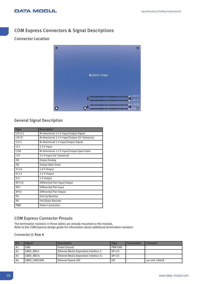
10 www.data- modul.com
COM Express Connectors & Signal Descriptions
Connector Location
General Signal Description
Type Description
I/O-3.3 Bi-directional 3.3 V Input/Output-Signal
I/O-5T Bi-directional 3.3 V Input/Output (5V Tolerance)
I/O-5 Bi-directional 5 V Input/Output-Signal
I3.3 3.3 V Input
I/OD Bi-directional 3.3 V Input/Output Open Drain
I-5T 3.3 V Input (5V Tolerance)
OA Output Analog
OD Output Open Drain
O-1.8 1.8 V Output
O-3.3 3.3 V Output
O-5 5 V Output
DP-I/O Differential Pair Input/Output
DP-I Differential Pair Input
DP-O Differential Pair Output
PU Pull-Up Resistor
PD Pull-Down Resistor
PWR Power Connection
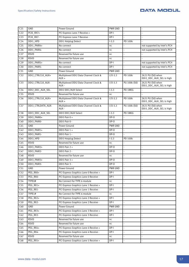
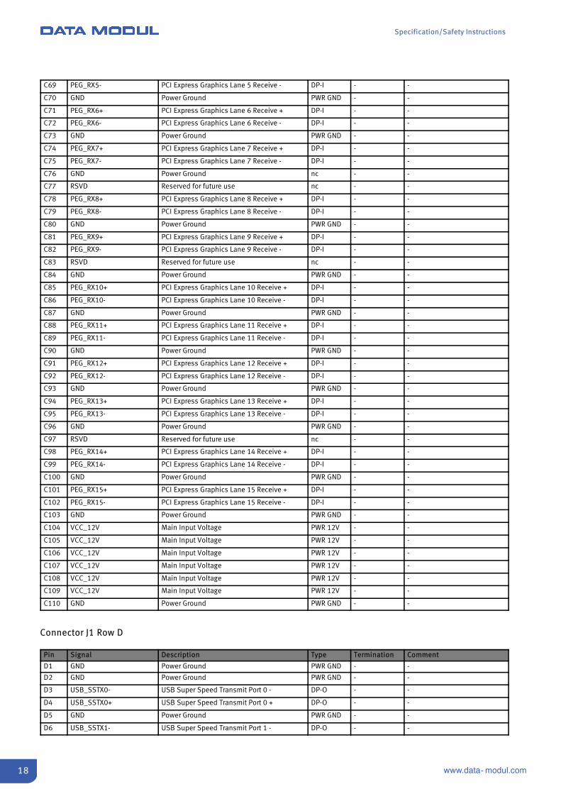
COM Express Connector PinoutsThe termination resistors in these tables are already mounted on the module.Refer to the COM Express design guide for information about additional termination resistors.
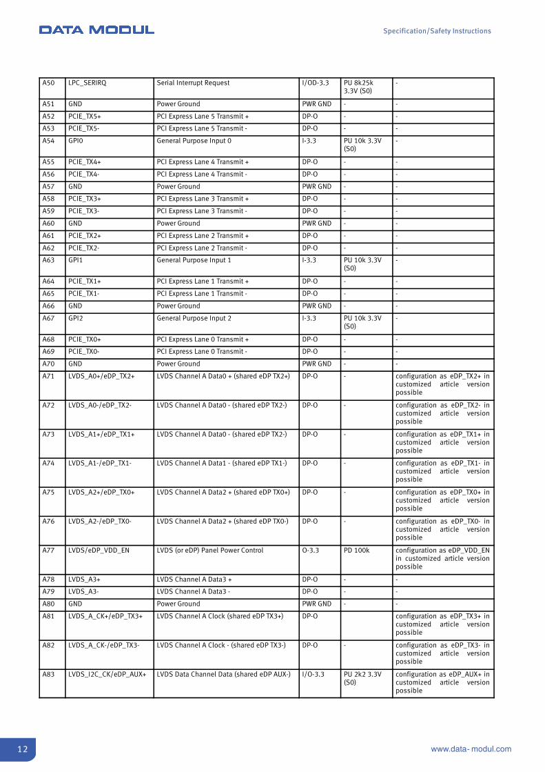
Connector J1 Row A
Pin Signal Description Type Termination Comment
A1 GND Power Ground PWR GND - -
A2 GBE0_MDI3- Ethernet Media Dependent Interface 3- DP-I/O - -
A3 GBE0_MDI3+ Ethernet Media Dependent Interface 3+ DP-I/O - -
A4 GBE0_LINK100# Ethernet Speed LED OD - can sink 100mA

Specification/Safety Instructions
11www.data- modul.com
A5 GBE0_LINK1000# Ethernet Speed LED OD - can sink 100mA
A6 GBE0_MDI2- Ethernet Media Dependent Interface 2 - DP-I/O - -
A7 GBE0_MDI2+ Ethernet Media Dependent Interface 2 + DP-I/O - -
A8 GBE0_LINK# LAN Link LED OD - can sink 100mA
A9 GBE0_MDI1- Ethernet Media Dependent Interface 1 - DP-I/O - -
A10 GBE0_MDI1+ Ethernet Media Dependent Interface 1 + DP-I/O - -
A11 GND Power Ground PWR GND - -
A12 GBE0_MDI0- Ethernet Media Dependent Interface 0 - DP-I/O - -
A13 GBE0_MDI0+ Ethernet Media Dependent Interface 0 + DP-I/O - -
A14 GBE0_CTREF Center Tab Reference Voltage O - 1μF capacitor to GND
A15 SUS_S3# Suspend To RAM (or deeper) Indicator 0-3.3 PD 20k -
A16 SATA0_TX+ SATA Transmit Pair 0 + DP-O - -
A17 SATA0_TX- SATA Transmit Pair 0 - DP-O - -
A18 SUS_S4# Suspend To Disk (or deeper) Indicator 0-3.3 PD 20k -
A19 SATA0_RX+ SATA Receive Pair 0 + DP-I - -
A20 SATA0_RX- SATA Receive Pair 0 - DP-I - -
A21 GND Power Ground PWR GND - -
A22 SATA2_TX+ SATA Transmit Pair 2 + DP-O - -
A23 SATA2_TX- SATA Transmit Pair 2 - DP-O - -
A24 SUS_S5# Soft Off Indicator O-3.3 PD 20k -
A25 SATA2_RX+ SATA Receive Pair 2 + DP-I
A26 SATA2_RX- SATA Receive Pair 2 - DP-I
A27 BATLOW# Battery Low I-3.3 PU 10k 3.3V(S5)
assertion will prevent wakefrom S3-S5 state
A28 (S)ATA_ACT# Serial ATA activity LED OD-3.3 PU 10k 3.3V(S0)
can sink 200mA
A29 AC/HDA_SYNC HD Audio Sync O-3.3 PD 15k in PCH -
A30 AC/HDA_RST# HD Audio Reset O-3.3 PD 15k in PCH -
A31 GND Power Ground PWR GND - -
A32 AC/HDA_BITCLK HD Audio Bit Clock Output O-3.3 PD 15k in PCH -
A33 AC/HDA_SDOUT HD Audio Serial Data Out O-3.3 PD 15k in PCH -
A34 BIOS_DIS0# BIOS Selection Strap 0 I-3.3 PU 100k 3.3V(SPI)
-
A35 THRMTRIP# Thermal Trip O-3.3 PU 10k 3.3V(S0)
do not use as this signal,because there is no differencebetween regular and over-temperature shutdown
A36 USB6- USB 2.0 Data Pair Port 6 - DP-I/O PD in PCH -
A37 USB6+ USB 2.0 Data Pair Port 6 + DP-I/O PD in PCH -
A38 USB_6_7_OC# USB Overcurrent Indicator Port 6/7 I-3.3 PU 10k 3.3V(S5)
-
A39 USB4- USB 2.0 Data Pair Port 4 - DP-I/O PD in PCH -
A40 USB4+ USB 2.0 Data Pair Port 4 + DP-I/O PD in PCH -
A41 GND Power Ground PWR GND - -
A42 USB2- USB 2.0 Data Pair Port 2 - DP-I/O PD in PCH -
A43 USB2+ USB 2.0 Data Pair Port 2 + DP-I/O PD in PCH -
A44 USB_2_3_OC# USB Overcurrent Indicator Port 2/3 I-3.3 PU 10k 3.3V(S5)
-
A45 USB0- USB 2.0 Data Pair Port 0 - DP-I/O PD in PCH -
A46 USB0+ USB 2.0 Data Pair Port 0 + DP-I/O PD in PCH -
A47 VCC_RTC Real-Time Clock Circuit Power Input PWR 3V - voltage range 2.7-3.47V
A48 EXCD0_PERST# Express Card Reset Port 0 O-3.3 - -
A49 EXCD0_CPPE# Express Card Capable Card Request Port 0 I-3.3 PU 10k 3.3V(S0)
-
Specification/Safety Instructions
12 www.data- modul.com
A50 LPC_SERIRQ Serial Interrupt Request I/OD-3.3 PU 8k25k3.3V (S0)
-
A51 GND Power Ground PWR GND - -
A52 PCIE_TX5+ PCI Express Lane 5 Transmit + DP-O - -
A53 PCIE_TX5- PCI Express Lane 5 Transmit - DP-O - -
A54 GPI0 General Purpose Input 0 I-3.3 PU 10k 3.3V(S0)
-
A55 PCIE_TX4+ PCI Express Lane 4 Transmit + DP-O - -
A56 PCIE_TX4- PCI Express Lane 4 Transmit - DP-O - -
A57 GND Power Ground PWR GND - -
A58 PCIE_TX3+ PCI Express Lane 3 Transmit + DP-O - -
A59 PCIE_TX3- PCI Express Lane 3 Transmit - DP-O - -
A60 GND Power Ground PWR GND - -
A61 PCIE_TX2+ PCI Express Lane 2 Transmit + DP-O - -
A62 PCIE_TX2- PCI Express Lane 2 Transmit - DP-O - -
A63 GPI1 General Purpose Input 1 I-3.3 PU 10k 3.3V(S0)
-
A64 PCIE_TX1+ PCI Express Lane 1 Transmit + DP-O - -
A65 PCIE_TX1- PCI Express Lane 1 Transmit - DP-O - -
A66 GND Power Ground PWR GND - -
A67 GPI2 General Purpose Input 2 I-3.3 PU 10k 3.3V(S0)
-
A68 PCIE_TX0+ PCI Express Lane 0 Transmit + DP-O - -
A69 PCIE_TX0- PCI Express Lane 0 Transmit - DP-O - -
A70 GND Power Ground PWR GND - -
A71 LVDS_A0+/eDP_TX2+ LVDS Channel A Data0 + (shared eDP TX2+) DP-O - configuration as eDP_TX2+ incustomized article versionpossible
A72 LVDS_A0-/eDP_TX2- LVDS Channel A Data0 - (shared eDP TX2-) DP-O - configuration as eDP_TX2- incustomized article versionpossible
A73 LVDS_A1+/eDP_TX1+ LVDS Channel A Data0 - (shared eDP TX2-) DP-O - configuration as eDP_TX1+ incustomized article versionpossible
A74 LVDS_A1-/eDP_TX1- LVDS Channel A Data1 - (shared eDP TX1-) DP-O - configuration as eDP_TX1- incustomized article versionpossible
A75 LVDS_A2+/eDP_TX0+ LVDS Channel A Data2 + (shared eDP TX0+) DP-O - configuration as eDP_TX0+ incustomized article versionpossible
A76 LVDS_A2-/eDP_TX0- LVDS Channel A Data2 + (shared eDP TX0-) DP-O - configuration as eDP_TX0- incustomized article versionpossible
A77 LVDS/eDP_VDD_EN LVDS (or eDP) Panel Power Control O-3.3 PD 100k configuration as eDP_VDD_ENin customized article versionpossible
A78 LVDS_A3+ LVDS Channel A Data3 + DP-O - -
A79 LVDS_A3- LVDS Channel A Data3 - DP-O - -
A80 GND Power Ground PWR GND - -
A81 LVDS_A_CK+/eDP_TX3+ LVDS Channel A Clock (shared eDP TX3+) DP-O configuration as eDP_TX3+ incustomized article versionpossible
A82 LVDS_A_CK-/eDP_TX3- LVDS Channel A Clock - (shared eDP TX3-) DP-O - configuration as eDP_TX3- incustomized article versionpossible
A83 LVDS_I2C_CK/eDP_AUX+ LVDS Data Channel Data (shared eDP AUX-) I/O-3.3 PU 2k2 3.3V(S0)
configuration as eDP_AUX+ incustomized article versionpossible
Specification/Safety Instructions
13www.data- modul.com
A84 LVDS_I2C_DAT/eDP_AUX- LVDS Data Channel Data (shared eDP AUX-) I/O-3.3 PU 2k2 3.3V(S0)
configuration as eDP_AUX- incustomized article versionpossible
A85 GPI3 General Purpose Input 3 I-3.3 PU 10k 3.3V(S0)
-
A86 RSVD Reserved for future use nc - -
A87 RSVD/eDP_HPD Reserved (shared eDP hot plug detection) nc/I-3.3 100k PD (opt) configuration as eDP_HPD incustomized article versionpossible
A88 PCIE_CLK_REF+ Reference PCI Express Clock + DP-O - -
A89 PCIE_CLK_REF- Reference PCI Express Clock - DP-O - -
A90 GND Power Ground PWR GND - -
A91 SPI_POWER 3.3V Power Output Pin for external SPI flash O-3.3 - -
A92 SPI_MISO SPI Master IN Slave OUT I-3.3 PU 20k in PCH All SPI signals are tri-statedwith 20k ohm PCH internalweak pull-up until reset isdeasserted.
A93 GPO0 General Purpose Output 0 O-3.3 PD 10k -
A94 SPI_CLK SPI Clock O-3.3 PU 20k in PCH All SPI signals are tri-statedwith 20k ohm PCH internalweak pull-up until reset isdeasserted.
A95 SPI_MOSI SPI Master Out Slave In O-3.3 PU 20k in PCH All SPI signals are tri-statedwith 20k ohm PCH internalweak pull-up until reset isdeasserted.
A96 TPM_PP No connect/TPM Physical Presence nc/I-3.3 100k PD configuration as TPM_PP incustomized article versionpossible
A97 TYPE10# No connect for TYPE 6 module nc - -
A98 SER0_TX Serial Port 0 TXD O-3.3 - 20V protection circuitimplemented on module, PDon carrier board needed forproper operation.
A99 SER0_RX Serial Port 0 RXD I-5T PU 47k 3.3V(S0)
20V protection circuitimplemented on module
A100 GND Power Ground PWR GND - -
A101 SER1_TX Serial Port 1 RXD O-3.3 - 20V protection circuitimplemented on module, PDon carrier board needed forproper operation.
A102 SER1_RX Serial Port 1 RXD I-5T PU 47k 3.3V(S0)
20V protection circuitimplemented on module
A103 LID# LID Switch Input I-3.3 PU 47k 3.3V(S5)
20V protection circuitimplemented on module
A104 VCC_12V Main Input Voltage PWR 12V - -
A105 VCC_12V Main Input Voltage PWR 12V - -
A106 VCC_12V Main Input Voltage PWR 12V - -
A107 VCC_12V Main Input Voltage PWR 12V - -
A108 VCC_12V Main Input Voltage PWR 12V - -
A109 VCC_12V Main Input Voltage PWR 12V - -
A110 GND Power Ground PWR GND - -
Connector J1 Row B
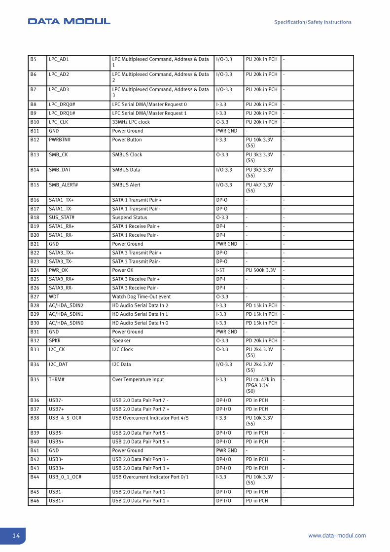
Pin Signal Description Type Termination Comment
B1 GND Power Ground PWR GND - -
B2 GBE0_ACT Ethernet Activity LED OD - can sink 100mA
B3 LPC_FRAME# LPC Frame Indicator O-3.3 - -
B4 LPC_AD0 LPC Multiplexed Command, Address & Data0
I/O-3.3 PU 20k in PCH -
Specification/Safety Instructions
14 www.data- modul.com
B5 LPC_AD1 LPC Multiplexed Command, Address & Data1
I/O-3.3 PU 20k in PCH -
B6 LPC_AD2 LPC Multiplexed Command, Address & Data2
I/O-3.3 PU 20k in PCH -
B7 LPC_AD3 LPC Multiplexed Command, Address & Data3
I/O-3.3 PU 20k in PCH -
B8 LPC_DRQ0# LPC Serial DMA/Master Request 0 I-3.3 PU 20k in PCH -
B9 LPC_DRQ1# LPC Serial DMA/Master Request 1 I-3.3 PU 20k in PCH -
B10 LPC_CLK 33MHz LPC clock O-3.3 PU 20k in PCH -
B11 GND Power Ground PWR GND - -
B12 PWRBTN# Power Button I-3.3 PU 10k 3.3V(S5)
-
B13 SMB_CK SMBUS Clock O-3.3 PU 3k3 3.3V(S5)
-
B14 SMB_DAT SMBUS Data I/O-3.3 PU 3k3 3.3V(S5)
-
B15 SMB_ALERT# SMBUS Alert I/O-3.3 PU 4k7 3.3V(S5)
-
B16 SATA1_TX+ SATA 1 Transmit Pair + DP-O - -
B17 SATA1_TX- SATA 1 Transmit Pair - DP-O - -
B18 SUS_STAT# Suspend Status O-3.3 - -
B19 SATA1_RX+ SATA 1 Receive Pair + DP-I - -
B20 SATA1_RX- SATA 1 Receive Pair - DP-I - -
B21 GND Power Ground PWR GND - -
B22 SATA3_TX+ SATA 3 Transmit Pair + DP-O - -
B23 SATA3_TX- SATA 3 Transmit Pair - DP-O - -
B24 PWR_OK Power OK I-5T PU 500k 3.3V -
B25 SATA3_RX+ SATA 3 Receive Pair + DP-I - -
B26 SATA3_RX- SATA 3 Receive Pair - DP-I - -
B27 WDT Watch Dog Time-Out event O-3.3 - -
B28 AC/HDA_SDIN2 HD Audio Serial Data In 2 I-3.3 PD 15k in PCH -
B29 AC/HDA_SDIN1 HD Audio Serial Data In 1 I-3.3 PD 15k in PCH -
B30 AC/HDA_SDIN0 HD Audio Serial Data In 0 I-3.3 PD 15k in PCH -
B31 GND Power Ground PWR GND - -
B32 SPKR Speaker O-3.3 PD 20k in PCH -
B33 I2C_CK I2C Clock O-3.3 PU 2k4 3.3V(S5)
-
B34 I2C_DAT I2C Data I/O-3.3 PU 2k4 3.3V(S5)
-
B35 THRM# Over Temperature Input I-3.3 PU ca. 47k inFPGA 3.3V(S0)
-
B36 USB7- USB 2.0 Data Pair Port 7 - DP-I/O PD in PCH -
B37 USB7+ USB 2.0 Data Pair Port 7 + DP-I/O PD in PCH -
B38 USB_4_5_OC# USB Overcurrent Indicator Port 4/5 I-3.3 PU 10k 3.3V(S5)
-
B39 USB5- USB 2.0 Data Pair Port 5 - DP-I/O PD in PCH -
B40 USB5+ USB 2.0 Data Pair Port 5 + DP-I/O PD in PCH -
B41 GND Power Ground PWR GND - -
B42 USB3- USB 2.0 Data Pair Port 3 - DP-I/O PD in PCH -
B43 USB3+ USB 2.0 Data Pair Port 3 + DP-I/O PD in PCH -
B44 USB_0_1_OC# USB Overcurrent Indicator Port 0/1 I-3.3 PU 10k 3.3V(S5)
-
B45 USB1- USB 2.0 Data Pair Port 1 - DP-I/O PD in PCH -
B46 USB1+ USB 2.0 Data Pair Port 1 + DP-I/O PD in PCH -

Specification/Safety Instructions
15www.data- modul.com
B47 EXCD1_PERST# Express Card Reset Port 1 O-3.3 - -
B48 EXCD1_CPPE# Express Card Capable Card Request Port 1 I-3.3 PU 10k 3.3V(S0)
-
B49 SYS_RESET# Reset Button Input O-3.3 PU 10k 3.3V(S0)
-
B50 CB_RESET# Carrier Board Reset O-3.3 - -
B51 GND Power Ground PWR GND - -
B52 PCIE_RX5+ PCI Express Lane 5 Receive + DP-I - -
B53 PCIE_RX5- PCI Express Lane 5 Receive - DP-I - -
B54 GPO1 General Purpose Output 1 O-3.3 PD 10k -
B55 PCIE_RX4+ PCI Express Lane 4 Receive + DP-I - -
B56 PCIE_RX4- PCI Express Lane 4 Receive - DP-I - -
B57 GPO2 General Purpose Output 2 O-3.3 PD 10k -
B58 PCIE_RX3+ PCI Express Lane 3 Receive + DP-I - -
B59 PCIE_RX3- PCI Express Lane 3 Receive - DP-I - -
B60 GND Power Ground PWR GND - -
B61 PCIE_RX2+ PCI Express Lane 2 Receive + DP-I - -
B62 PCIE_RX2- PCI Express Lane 2 Receive - DP-I - -
B63 GPO3 General Purpose Output 3 O-3.3 PD 10k -
B64 PCIE_RX1+ PCI Express Lane 1 Receive + DP-I - -
B65 PCIE_RX1- PCI Express Lane 1 Receive - DP-I - -
B66 WAKE0# PCI Express Wake Event I-3.3 PU 10k 3.3V(S5)
-
B67 WAKE1# General Purpose Wake Event I-3.3 PU 10k 3.3V(S5)
-
B68 PCIE_RX0+ PCI Express Lane 0 Receive + DP-I - -
B69 PCIE_RX0- PCI Express Lane 0 Receive - DP-I - -
B70 GND Power Ground PWR GND - -
B71 LVDS_B0+ LVDS Channel B Data0 + DP-O - -
B72 LVDS_B0- LVDS Channel B Data0 - DP-O - -
B73 LVDS_B1+ LVDS Channel B Data1 + DP-O - -
B74 LVDS_B1- LVDS Channel B Data1 - DP-O - -
B75 LVDS_B2+ LVDS Channel B Data2 + DP-O - -
B76 LVDS_B2- LVDS Channel B Data2 - DP-O - -
B77 LVDS_B3+ LVDS Channel B Data3 + DP-O - -
B78 LVDS_B3- LVDS Channel B Data3 - DP-O - -
B79 LVDS/eDP_BKLT_EN Panel Backlight On O-3.3 PD 100k configuration as eDP_BKLT_ENin customized article versionpossible
B80 GND Power Ground PWR GND - -
B81 LVDS_B_CK+ LVDS Channel B Clock + DP-O - -
B82 LVDS_B_CK- LVDS Channel B Clock - DP-O - -
B83 LVDS_BKLT_CTRL Backlight Brightness Control O-3.3 PD 100k configuration aseDB_BKLT_CTRL …
B84 VCC_5V_SBY 5V Standby PWR 5V(S5)
- optional (not necessary insingle supply mode)
B85 VCC_5V_SBY 5V Standby PWR 5V(S5)
- optional (not necessary insingle supply mode)
B86 VCC_5V_SBY 5V Standby PWR 5V(S5)
- optional (not necessary insingle supply mode)
B87 VCC_5V_SBY 5V Standby PWR 5V(S5)
- optional (not necessary insingle supply mode)
B88 BIOS_DIS1# BIOS Selection Strap 1 I-3.3 PU 100k 3.3V(SPI)
-

Specification/Safety Instructions
16 www.data- modul.com
B89 VGA_RED No connect/Red Analog Video Output nc/OA PD 150R optional in product versionswith assembled VGA-Bridge
B90 GND Power Ground PWR GND - -
B91 VGA_GRN No connect/Green Analog Video Output nc/OA PD 150R
optional in product versionswith assembled VGA-Bridge
B92 VGA_BLU No connect/Blue Analog Video Output nc/OA PD 150R
B93 VGA_HSYNC No connect/VGA Horizontal Synchronisation nc/O-3.3 -
B94 VGA_VSYNC No connect/VGA Vertical Synchronization nc/O-3.3 -
B95 VGA_I2C_CK No connect/VGA Data Channel Clock nc/I/O-3.3 PU 1k 3.3V(S0)
B96 VGA_I2C_DAT No connect/VGA Data Channel Data nc/I/O-3.3 PU 1k 3.3V(S0)
B97 SPI_CS# SPI Chip Select O-3.3 - -
B98 RSVD Reserved for future use nc - -
B99 RSVD Reserved for future use nc - -
B100 GND Power Ground PWR GND - -
B101 FAN_PWMOUT Fan PWM Output O-3.3 - 20V protection circuitimplemented on module, PDon carrier board needed forproper operation.
B102 FAN_TACHIN Fan Tach Input I-3.3 PU 10k 3.3V(S0)
20V protection circuitimplemented on module
B103 SLEEP# Sleep Button Input I-3.3 PU 47k 3.3V(S5)
20V protection circuitimplemented on module
B104 VCC_12V Main Input Voltage PWR 12V - -
B105 VCC_12V Main Input Voltage PWR 12V - -
B106 VCC_12V Main Input Voltage PWR 12V - -
B107 VCC_12V Main Input Voltage PWR 12V - -
B108 VCC_12V Main Input Voltage PWR 12V - -
B109 VCC_12V Main Input Voltage PWR 12V - -
B110 GND Power Ground PWR GND - -
Connector J1 Row C
Pin Signal Description Type Termination Comment
C1 GND Power Ground PWR GND - -
C2 GND Power Ground PWR GND - -
C3 USB_SSRX0- USB Super Speed Receive Port 0 - DP-I - -
C4 USB_SSRX0+ USB Super Speed Receive Port 0 + DP-I - -
C5 GND Power Ground PWR GND - -
C6 USB_SSRX1- USB Super Speed Receive Port 1 - DP-I - -
C7 USB_SSRX1+ USB Super Speed Receive Port 1 + DP-I - -
C8 GND Power Ground PWR GND - -
C9 USB_SSRX2- USB Super Speed Receive Port 2 - DP-I - -
C10 USB_SSRX2+ USB Super Speed Receive Port 2 + DP-I - -
C11 GND Power Ground PWR GND - -
C12 USB_SSRX3- USB Super Speed Receive Port 3 - DP-I - -
C13 USB_SSRX3+ USB Super Speed Receive Port 3+ DP-I - -
C14 GND Power Ground PWR GND - -
C15 DDI1_PAIR6+ No connect nc - not supported by Intel's PCH
C16 DDI1_PAIR6- No connect nc - not supported by Intel's PCH
C17 RSVD Reserved for future use nc - -
C18 RSVD Reserved for future use nc - -
C19 PCIE_RX6+ PCI Express Lane 6 Receive + DP-I - -
C20 PCIE_RX6- PCI Express Lane 6 Receive - DP-I - -
Specification/Safety Instructions
17www.data- modul.com
C21 GND Power Ground PWR GND - -
C22 PCIE_RX7+ PCI Express Lane 7 Receive + DP-I - -
C23 PCIE_RX7- PCI Express Lane 7 Receive - DP-I - -
C24 DDI1_HPD DDI1 Hotplug Detect I-3.3 PD 100k -
C25 DDI1_PAIR4+ No connect nc - not supported by Intel's PCH
C26 DDI1_PAIR4- No connect nc - not supported by Intel's PCH
C27 RSVD Reserved for future use nc - -
C28 RSVD Reserved for future use nc - -
C29 DDI1_PAIR5+ No connect DP-I - not supported by Intel's PCH
C30 DDI1_PAIR5- No connect DP-I - not supported by Intel's PCH
C31 GND Power Ground PWR GND - -
C32 DDI2_CTRLCLK_AUX+ Multiplexed DDI2 Data Channel Clock &AUX +
I/O-3.3 PD 100k 2k21 PU (S0) whenDDI2_DDC_AUX_SEL is high
C33 DDI2_CTRLCLK_AUX- Multiplexed DDI2 Data Channel Clock &AUX -
I/O-3.3 PU 100k (S0) 2k21 PU (S0) whenDDI2_DDC_AUX_SEL is high
C34 DDI2_DDC_AUX_SEL DDI2 DDC/AUX Select I-3.3 PD 1MEG -
C35 RSVD Reserved for future use nc - -
C36 DDI3_CTRLCLK_AUX+ Multiplexed DDI3 Data Channel Clock &AUX +
I/O-3.3 PD 100k 2k21 PU (S0) whenDDI3_DDC_AUX_SEL is high
C37 DDI3_CTRLDATA_AUX- Multiplexed DDI3 Data Channel Clock &AUX -
I/O-3.3 PU 100k (S0) 2k21 PU (S0) whenDDI3_DDC_AUX_SEL is high
C38 DDI3_DDC_AUX_SEL DDI3 DDC/AUX Select I-3.3 PD 1MEG -
C39 DDI3_PAIR0+ DDI3 Pair 0 + DP-O - -
C40 DDI3_PAIR0- DDI3 Pair 0 - DP-O - -
C41 GND Power Ground PWR GND - -
C42 DDI3_PAIR1+ DDI3 Pair 1 + DP-O - -
C43 DDI3_PAIR1- DDI3 Pair 1 - DP-O - -
C44 DDI3_HPD DDI3 Hotplug Detect I-3.3 PD 100k -
C45 RSVD Reserved for future use nc - -
C46 DDI3_PAIR2+ DDI3 Pair 2 + DP-O - -
C47 DDI3_PAIR2- DDI3 Pair 2 - DP-O - -
C48 RSVD Reserved for future use nc - -
C49 DDI3_PAIR3+ DDI3 Pair 3 + DP-O - -
C50 DDI3_PAIR3- DDI3 Pair 3 - DP-O - -
C51 GND Power Ground PWR GND - -
C52 PEG_RX0+ PCI Express Graphics Lane 0 Receive + DP-I - -
C53 PEG_RX0- PCI Express Graphics Lane 0 Receive - DP-I - -
C54 TYPE0# No Connect for TYPE 6 module nc - -
C55 PEG_RX1+ PCI Express Graphics Lane 1 Receive + DP-I - -
C56 PEG_RX1- PCI Express Graphics Lane 1 Receive - DP-I - -
C57 TYPE1# No Connect for TYPE 6 module nc - -
C58 PEG_RX2+ PCI Express Graphics Lane 2 Receive + DP-I - -
C59 PEG_RX2- PCI Express Graphics Lane 2 Receive - DP-I - -
C60 GND Power Ground PWR GND - -
C61 PEG_RX3+ PCI Express Graphics Lane 3 Receive + DP-I - -
C62 PEG_RX3- PCI Express Graphics Lane 3 Receive - DP-I - -
C63 RSVD Reserved for future use nc - -
C64 RSVD Reserved for future use nc - -
C65 PEG_RX4+ PCI Express Graphics Lane 4 Receive + DP-I - -
C66 PEG_RX4- PCI Express Graphics Lane 4 Receive - DP-I - -
C67 RSVD Reserved for future use nc - -
C68 PEG_RX5+ PCI Express Graphics Lane 5 Receive + DP-I - -
Specification/Safety Instructions
18 www.data- modul.com
C69 PEG_RX5- PCI Express Graphics Lane 5 Receive - DP-I - -
C70 GND Power Ground PWR GND - -
C71 PEG_RX6+ PCI Express Graphics Lane 6 Receive + DP-I - -
C72 PEG_RX6- PCI Express Graphics Lane 6 Receive - DP-I - -
C73 GND Power Ground PWR GND - -
C74 PEG_RX7+ PCI Express Graphics Lane 7 Receive + DP-I - -
C75 PEG_RX7- PCI Express Graphics Lane 7 Receive - DP-I - -
C76 GND Power Ground nc - -
C77 RSVD Reserved for future use nc - -
C78 PEG_RX8+ PCI Express Graphics Lane 8 Receive + DP-I - -
C79 PEG_RX8- PCI Express Graphics Lane 8 Receive - DP-I - -
C80 GND Power Ground PWR GND - -
C81 PEG_RX9+ PCI Express Graphics Lane 9 Receive + DP-I - -
C82 PEG_RX9- PCI Express Graphics Lane 9 Receive - DP-I - -
C83 RSVD Reserved for future use nc - -
C84 GND Power Ground PWR GND - -
C85 PEG_RX10+ PCI Express Graphics Lane 10 Receive + DP-I - -
C86 PEG_RX10- PCI Express Graphics Lane 10 Receive - DP-I - -
C87 GND Power Ground PWR GND - -
C88 PEG_RX11+ PCI Express Graphics Lane 11 Receive + DP-I - -
C89 PEG_RX11- PCI Express Graphics Lane 11 Receive - DP-I - -
C90 GND Power Ground PWR GND - -
C91 PEG_RX12+ PCI Express Graphics Lane 12 Receive + DP-I - -
C92 PEG_RX12- PCI Express Graphics Lane 12 Receive - DP-I - -
C93 GND Power Ground PWR GND - -
C94 PEG_RX13+ PCI Express Graphics Lane 13 Receive + DP-I - -
C95 PEG_RX13- PCI Express Graphics Lane 13 Receive - DP-I - -
C96 GND Power Ground PWR GND - -
C97 RSVD Reserved for future use nc - -
C98 PEG_RX14+ PCI Express Graphics Lane 14 Receive + DP-I - -
C99 PEG_RX14- PCI Express Graphics Lane 14 Receive - DP-I - -
C100 GND Power Ground PWR GND - -
C101 PEG_RX15+ PCI Express Graphics Lane 15 Receive + DP-I - -
C102 PEG_RX15- PCI Express Graphics Lane 15 Receive - DP-I - -
C103 GND Power Ground PWR GND - -
C104 VCC_12V Main Input Voltage PWR 12V - -
C105 VCC_12V Main Input Voltage PWR 12V - -
C106 VCC_12V Main Input Voltage PWR 12V - -
C107 VCC_12V Main Input Voltage PWR 12V - -
C108 VCC_12V Main Input Voltage PWR 12V - -
C109 VCC_12V Main Input Voltage PWR 12V - -
C110 GND Power Ground PWR GND - -
Connector J1 Row D
Pin Signal Description Type Termination Comment
D1 GND Power Ground PWR GND - -
D2 GND Power Ground PWR GND - -
D3 USB_SSTX0- USB Super Speed Transmit Port 0 - DP-O - -
D4 USB_SSTX0+ USB Super Speed Transmit Port 0 + DP-O - -
D5 GND Power Ground PWR GND - -
D6 USB_SSTX1- USB Super Speed Transmit Port 1 - DP-O - -

Specification/Safety Instructions
19www.data- modul.com
D7 USB_SSTX1+ USB Super Speed Transmit Port 1 + DP-O - -
D8 GND Power Ground PWR GND - -
D9 USB_SSTX2- USB Super Speed Transmit Port 2 - DP-O - -
D10 USB_SSTX2+ USB Super Speed Transmit Port 2+ DP-O - -
D11 GND Power Ground PWR GND - -
D12 USB_SSTX3- USB Super Speed Transmit Port 3 - DP-O - -
D13 USB_SSTX3+ USB Super Speed Transmit Port 3 + DP-O - -
D14 GND Power Ground PWR GND - -
D15 DDI1_CTRLCLK_AUX+ Multiplexed DDI1 Data Channel Clock &AUX +
I/O-3.3 PD 100k 2k21 PU (S0) whenDDI1_DDC_AUX_SEL is high
D16 DDI1_CTRLDATA_AUX- Multiplexed DDI1 Data Channel Clock &AUX -
I/O-3.3 PU 100k (S0) 2k21 PU (S0) whenDDI1_DDC_AUX_SEL is high
D17 RSVD Reserved for future use nc - -
D18 RSVD Reserved for future use nc - -
D19 PCIE_TX6+ PCI Express Lane 6 Transmit + DP-O - -
D20 PCIE_TX6- PCI Express Lane 6 Transmit - DP-O - -
D21 GND Power Ground PWR GND - -
D22 PCIE_TX7+ PCI Express Lane 7 Transmit + DP-O - -
D23 PCIE_TX7- PCI Express Lane 7 Transmit - DP-O - -
D24 RSVD Reserved for future use nc - -
D25 RSVD Reserved for future use nc - -
D26 DDI1_PAIR0+ DDI1 Pair 0 + DP-O - -
D27 DDI1_PAIR0- DDI1 Pair 0 - DP-O - -
D28 RSVD Reserved for future use nc - -
D29 DDI1_PAIR1+ DDI1 Pair 1 + DP-O - -
D30 DDI1_PAIR1- DDI1 Pair 1 - DP-O - -
D31 GND Power Ground PWR GND - -
D32 DDI1_PAIR2+ DDI1 Pair 2 + DP-O - -
D33 DDI1_PAIR2- DDI1 Pair 2 - DP-O - -
D34 DDI1_DDC_AUX_SEL DDI1 DDC/AUX Select I-3.3 PD 1 MEG -
D35 RSVD Reserved for future use nc - -
D36 DDI1_PAIR3+ DDI1 Pair 3 + DP-O - -
D37 DDI1_PAIR3- DDI1 Pair 3- DP-O - -
D38 RSVD Reserved for future use nc - -
D39 DDI2_PAIR0+ DDI2 Pair 0 + DP-O - -
D40 DDI2_PAIR0- DDI2 Pair 0 - DP-O - -
D41 GND Power Ground PWR GND - -
D42 DDI2_PAIR1+ DDI2 Pair 1 + DP-O - -
D43 DDI2_PAIR1- DDI2 Pair 1 - DP-O - -
D44 DDI2_HPD DDI2 Hotplug Detect I-3.3 PD 100k -
D45 RSVD Reserved for future use nc - -
D46 DDI2_PAIR2+ DDI2 Pair 2 + DP-O - -
D47 DDI2_PAIR2- DDI2 Pair 2 - DP-O - -
D48 RSVD Reserved for future use nc - -
D49 DDI2_PAIR3+ DDI2 Pair 3 + DP-O - -
D50 DDI2_PAIR3- DDI2 Pair 3- DP-O - -
D51 GND Power Ground PWR GND -
D52 PEG_TX0+ PCI Express Graphics Lane 0 Transmit + DP-O - -
D53 PEG_TX0- PCI Express Graphics Lane 0 Transmit - DP-O - -
D54 PEG_Lane_RV# PCI Express Graphics Lane Reversal I-3.3 PU 10k 3.3V(S0)
-
D55 PEG_TX1+ PCI Express Graphics Lane 1 Transmit + DP-O - -

Specification/Safety Instructions
20 www.data- modul.com
D56 PEG_TX1- PCI Express Graphics Lane 1 Transmit - DP-O - -
D57 TYPE2# Connected to GND for TYPE 6 module PWR GND - -
D58 PEG_TX2+ PCI Express Graphics Lane 2 Transmit + DP-O - -
D59 PEG_TX2- PCI Express Graphics Lane 2 Transmit - DP-O - -
D60 GND Power Ground PWR GND - -
D61 PEG_TX3+ PCI Express Graphics Lane 3 Transmit + DP-O - -
D62 PEG_TX3- PCI Express Graphics Lane 3 Transmit - DP-O - -
D63 RSVD Reserved for future use nc - -
D64 RSVD Reserved for future use nc - -
D65 PEG_TX4+ PCI Express Graphics Lane 4 Transmit + DP-O - -
D66 PEG_TX4- PCI Express Graphics Lane 4 Transmit - DP-O - -
D67 GND Power Ground PWR GND - -
D68 PEG_TX5+ PCI Express Graphics Lane 5 Transmit + DP-O - -
D69 PEG_TX5- PCI Express Graphics Lane 5 Transmit - DP-O - -
D70 GND Power Ground PWR GND - -
D71 PEG_TX6+ PCI Express Graphics Lane 6 Transmit + DP-O - -
D72 PEG_TX6- PCI Express Graphics Lane 6 Transmit - DP-O - -
D73 GND Power Ground PWR GND - -
D74 PEG_TX7+ PCI Express Graphics Lane 7 Transmit + DP-O - -
D75 PEG_TX7- PCI Express Graphics Lane 7 Transmit - DP-O - -
D76 GND Power Ground PWR GND - -
D77 RSVD Reserved for future use nc - -
D78 PEG_TX8+ PCI Express Graphics Lane 8 Transmit + DP-O - -
D79 PEG_TX8- PCI Express Graphics Lane 8 Transmit - DP-O - -
D80 GND Power Ground PWR GND - -
D81 PEG_TX9+ PCI Express Graphics Lane 9 Transmit + DP-O - -
D82 PEG_TX9- PCI Express Graphics Lane 9 Transmit - DP-O - -
D83 RSVD Reserved for future use nc - -
D84 GND Power Ground PWR GND - -
D85 PEG_TX10+ PCI Express Graphics Lane 10 Transmit + DP-O - -
D86 PEG_TX10- PCI Express Graphics Lane 10 Transmit - DP-O - -
D87 GND Power Ground PWR GND - -
D88 PEG_TX11+ PCI Express Graphics Lane 11 Transmit + DP-O - -
D89 PEG_TX11- PCI Express Graphics Lane 11 Transmit - DP-O - -
D90 GND Power Ground PWR GND - -
D91 PEG_TX12+ PCI Express Graphics Lane 12 Transmit + DP-O - -
D92 PEG_TX12- PCI Express Graphics Lane 12 Transmit - DP-O - -
D93 GND Power Ground PWR GND - -
D94 PEG_TX13+ PCI Express Graphics Lane 13 Transmit + DP-O - -
D95 PEG_TX13- PCI Express Graphics Lane 13 Transmit - DP-O - -
D96 GND Power Ground PWR GND - -
D97 RSVD Reserved for future use nc - -
D98 PEG_TX14+ PCI Express Graphics Lane 14 Transmit + DP-O - -
D99 PEG_TX14- PCI Express Graphics Lane 14 Transmit - DP-O - -
D100 GND Power Ground PWR GND - -
D101 PEG_TX15+ PCI Express Graphics Lane 15 Transmit + DP-O - -
D102 PEG_TX15- PCI Express Graphics Lane 15 Transmit - DP-O - -
D103 GND Power Ground PWR GND - -
D104 VCC_12V Main Input Voltage PWR 12V - -
D105 VCC_12V Main Input Voltage PWR 12V - -
D106 VCC_12V Main Input Voltage PWR 12V - -

Specification/Safety Instructions
21www.data- modul.com
D107 VCC_12V Main Input Voltage PWR 12V - -
D108 VCC_12V Main Input Voltage PWR 12V - -
D109 VCC_12V Main Input Voltage PWR 12V - -
D110 GND Power Ground PWR GND - -
Specification/Safety Instructions
22 www.data- modul.com
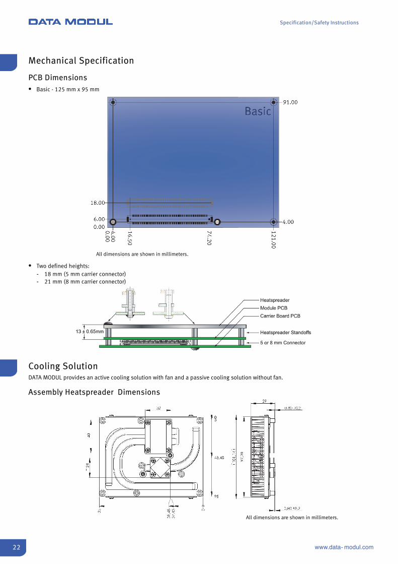
Mechanical Specification
PCB DimensionsS Basic - 125 mm x 95 mm
All dimensions are shown in millimeters.
S Two defined heights:- 18 mm (5 mm carrier connector)- 21 mm (8 mm carrier connector)
Cooling SolutionDATA MODUL provides an active cooling solution with fan and a passive cooling solution without fan.
Assembly Heatspreader Dimensions
All dimensions are shown in millimeters.
Specification/Safety Instructions
23www.data- modul.com
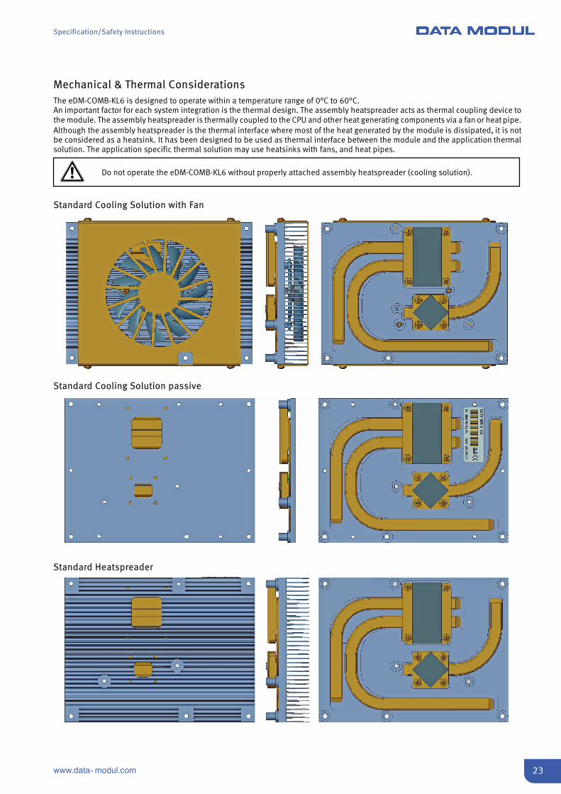
Mechanical & Thermal ConsiderationsThe eDM-COMB-KL6 is designed to operate within a temperature range of 0°C to 60°C.An important factor for each system integration is the thermal design. The assembly heatspreader acts as thermal coupling device tothe module. The assembly heatspreader is thermally coupled to the CPU and other heat generating components via a fan or heat pipe.Although the assembly heatspreader is the thermal interface where most of the heat generated by the module is dissipated, it is notbe considered as a heatsink. It has been designed to be used as thermal interface between the module and the application thermalsolution. The application specific thermal solution may use heatsinks with fans, and heat pipes.
Do not operate the eDM-COMB-KL6 without properly attached assembly heatspreader (cooling solution).
Standard Cooling Solution with Fan
Standard Cooling Solution passive
Standard Heatspreader
Specification/Safety Instructions
24 www.data- modul.com
BIOS SetupThe purpose of this chapter is to describe the settings in the UEFI BIOS Setup program on this Computer on Module and to explain theprocedure for updating the UEFI BIOS.
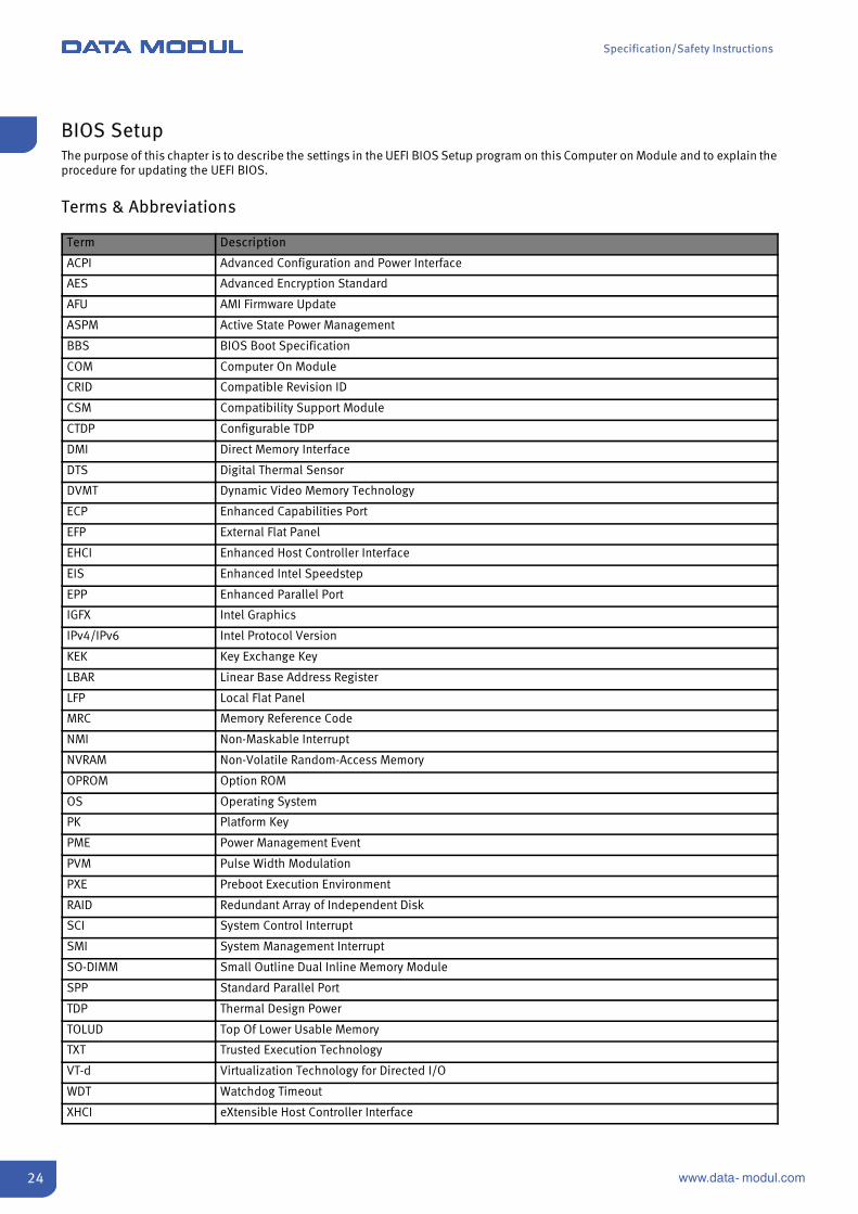
Terms & Abbreviations
Term Description
ACPI Advanced Configuration and Power Interface
AES Advanced Encryption Standard
AFU AMI Firmware Update
ASPM Active State Power Management
BBS BIOS Boot Specification
COM Computer On Module
CRID Compatible Revision ID
CSM Compatibility Support Module
CTDP Configurable TDP
DMI Direct Memory Interface
DTS Digital Thermal Sensor
DVMT Dynamic Video Memory Technology
ECP Enhanced Capabilities Port
EFP External Flat Panel
EHCI Enhanced Host Controller Interface
EIS Enhanced Intel Speedstep
EPP Enhanced Parallel Port
IGFX Intel Graphics
IPv4/IPv6 Intel Protocol Version
KEK Key Exchange Key
LBAR Linear Base Address Register
LFP Local Flat Panel
MRC Memory Reference Code
NMI Non-Maskable Interrupt
NVRAM Non-Volatile Random-Access Memory
OPROM Option ROM
OS Operating System
PK Platform Key
PME Power Management Event
PVM Pulse Width Modulation
PXE Preboot Execution Environment
RAID Redundant Array of Independent Disk
SCI System Control Interrupt
SMI System Management Interrupt
SO-DIMM Small Outline Dual Inline Memory Module
SPP Standard Parallel Port
TDP Thermal Design Power
TOLUD Top Of Lower Usable Memory
TXT Trusted Execution Technology
VT-d Virtualization Technology for Directed I/O
WDT Watchdog Timeout
XHCI eXtensible Host Controller Interface

Specification/Safety Instructions
25www.data- modul.com
BIOS Update Description
This COM is provided with an American Megatrends, Inc. Aptio V UEFI Firmware. Please use the AMI Firmware Update (AFU) utility suitefor updating the BIOS. This is a scriptable command line tool, utilized for factory or field BIOS updates. It is available for DOS, MicrosoftWindows®, Linux, FreeBSD and the UEFI shell.Please contact your DATA MODUL support for accessing the tools.
The complete UEFI Firmware image for this eDM-COM Board consists of the following parts:
S Main BIOS: Responsible for main hardware initialization and feature interfaces during runtime.
S Boot Block: Minimal hardware initialization and provides recovery functionality.
S NVRAM: Stores configuration variables.
S Management Engine: Intel® ME firmware binary.
S GbE Region: Stores Gigabit-Ethernet configuration data.
For updating the complete 16MB firmware image with the UEFI version of AFU use following command:
S afuefix64.efi newbiosfile.bin /P /B /N /ME /X.
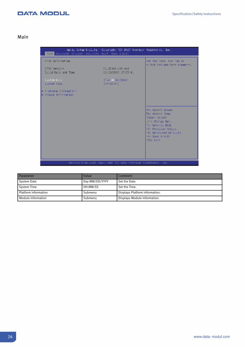
BIOS Setup DescriptionThe UEFI Setup program allows users to modify the basic system configuration and save these settings to NVRAM.
To enter UEFI Setup, press DEL or ESC during POST.
To select a Boot Popup Menu, press F7 during POST. At End of Post a selection menu will show all available boot devices to choose from.UEFI Setup program can be entered from Boot Popup Menu as well.
Following is a description of the UEFI Setup pages.
Specification/Safety Instructions
26 www.data- modul.com
Main
Parameter Value Comment
System Date Day MM/DD/YYYY Set the Date.
System Time HH:MM:SS Set the Time.
Platform Information Submenu Displays Platform Information.
Module Information Submenu Displays Module Information.
Specification/Safety Instructions
27www.data- modul.com
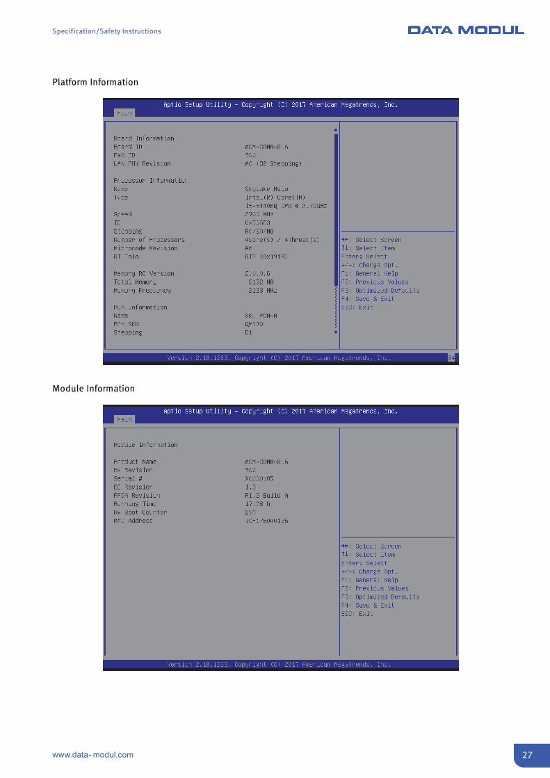
Platform Information
Module Information

Specification/Safety Instructions
28 www.data- modul.com
Advanced
Parameter Value Comment
CPU Configuration Submenu CPU Configuration Parameters
Power & Performance Submenu Power & Performance Options
Trusted Computing Submenu Trusted Computing (TPM) Settings
Serial Port Console Redirection Submenu Serial Port Console Redirection Settings
PCH-FW Configuration Submenu Configure Management Engine Parameters
Thermal Configuration Submenu Thermal Configuration Parameters
SIO Configuration Submenu SuperIO Settings
Network Stack Configuration Submenu Network Stack Settings
CSM Configuration Submenu Compatibility Support Module Settings
USB Configuration Submenu USB Configuration Parameters
Module Peripherals Configuration Submenu Configure Module Peripherals
Module H/W Monitor Submenu Monitor hardware status
Module Watchdog Configuration Submenu Configure Watchdog
Module Display Configuration Submenu Configure Module Display options

Specification/Safety Instructions
29www.data- modul.com
CPU Configuration
Parameter Value Comment
Hardware Prefetcher EnabledDisabled
Enable/Disable the Mid Level Cache (L2) streamer prefetcher.
Adjacent Cache Line Prefetch EnabledDisabled
Enable/Disable the Mid Level Cache (L2) prefetching of adjacent cachelines.
Intel Virtualization Technology EnabledDisabled
When enabled, a VMM can utilize the additional hardware capabilitiesprovided by Vanderpool Technology.
AES EnabledDisabled
Enable/Disable CPU Advanced Encryption Standard instructions.
Specification/Safety Instructions
30 www.data- modul.com
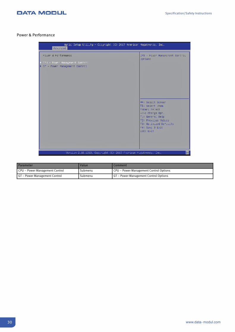
Power & Performance
Parameter Value Comment
CPU – Power Management Control Submenu CPU – Power Management Control Options
GT – Power Management Control Submenu GT – Power Management Control Options
Specification/Safety Instructions
31www.data- modul.com
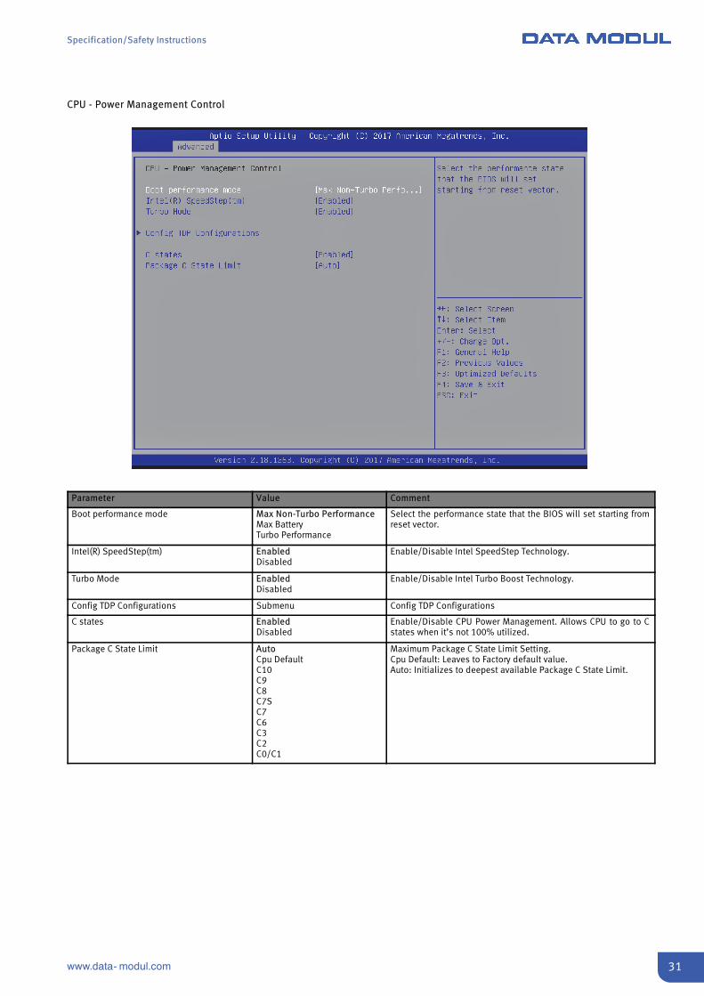
CPU - Power Management Control
Parameter Value Comment
Boot performance mode Max Non-Turbo PerformanceMax BatteryTurbo Performance
Select the performance state that the BIOS will set starting fromreset vector.
Intel(R) SpeedStep(tm) EnabledDisabled
Enable/Disable Intel SpeedStep Technology.
Turbo Mode EnabledDisabled
Enable/Disable Intel Turbo Boost Technology.
Config TDP Configurations Submenu Config TDP Configurations
C states EnabledDisabled
Enable/Disable CPU Power Management. Allows CPU to go to Cstates when it’s not 100% utilized.
Package C State Limit AutoCpu DefaultC10C9C8C7SC7C6C3C2C0/C1
Maximum Package C State Limit Setting.Cpu Default: Leaves to Factory default value.Auto: Initializes to deepest available Package C State Limit.
Specification/Safety Instructions
32 www.data- modul.com
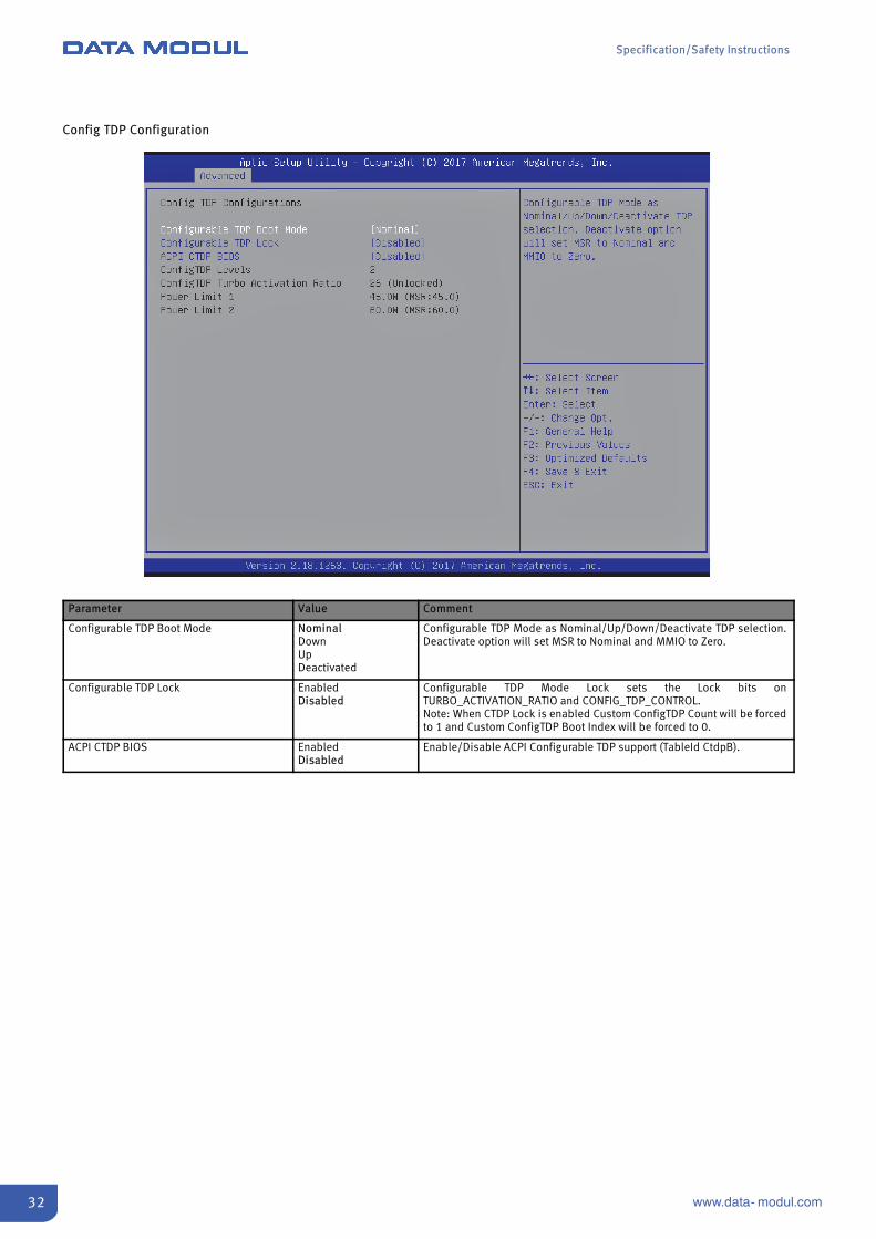
Config TDP Configuration
Parameter Value Comment
Configurable TDP Boot Mode NominalDownUpDeactivated
Configurable TDP Mode as Nominal/Up/Down/Deactivate TDP selection.Deactivate option will set MSR to Nominal and MMIO to Zero.
Configurable TDP Lock EnabledDisabled
Configurable TDP Mode Lock sets the Lock bits onTURBO_ACTIVATION_RATIO and CONFIG_TDP_CONTROL.Note: When CTDP Lock is enabled Custom ConfigTDP Count will be forcedto 1 and Custom ConfigTDP Boot Index will be forced to 0.
ACPI CTDP BIOS EnabledDisabled
Enable/Disable ACPI Configurable TDP support (TableId CtdpB).

Specification/Safety Instructions
33www.data- modul.com
GT - Power Management Control
Parameter Value Comment
RC6 (Render Standby) EnabledDisabled
Enable/Disable render standby support.
Specification/Safety Instructions
34 www.data- modul.com
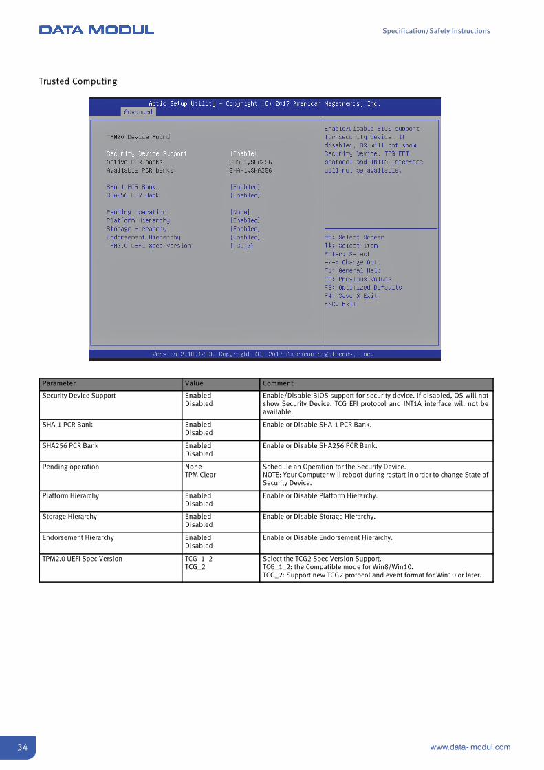
Trusted Computing
Parameter Value Comment
Security Device Support EnabledDisabled
Enable/Disable BIOS support for security device. If disabled, OS will notshow Security Device. TCG EFI protocol and INT1A interface will not beavailable.
SHA-1 PCR Bank EnabledDisabled
Enable or Disable SHA-1 PCR Bank.
SHA256 PCR Bank EnabledDisabled
Enable or Disable SHA256 PCR Bank.
Pending operation NoneTPM Clear
Schedule an Operation for the Security Device.NOTE: Your Computer will reboot during restart in order to change State ofSecurity Device.
Platform Hierarchy EnabledDisabled
Enable or Disable Platform Hierarchy.
Storage Hierarchy EnabledDisabled
Enable or Disable Storage Hierarchy.
Endorsement Hierarchy EnabledDisabled
Enable or Disable Endorsement Hierarchy.
TPM2.0 UEFI Spec Version TCG_1_2TCG_2
Select the TCG2 Spec Version Support.TCG_1_2: the Compatible mode for Win8/Win10.TCG_2: Support new TCG2 protocol and event format for Win10 or later.

Specification/Safety Instructions
35www.data- modul.com
Serial Port Console Redirection
Parameter Value Comment
Console Redirection EnabledDisabled
Enables/Disables Console Redirection.
Console Redirection Settings Submenu The settings specify how the host computer and the remote computer(which the user is using) will exchange data. Both computers should havethe same or compatible settings.
Legacy Console Redirection Settings Submenu Configure Port for Legacy Console Redirection.
Specification/Safety Instructions
36 www.data- modul.com
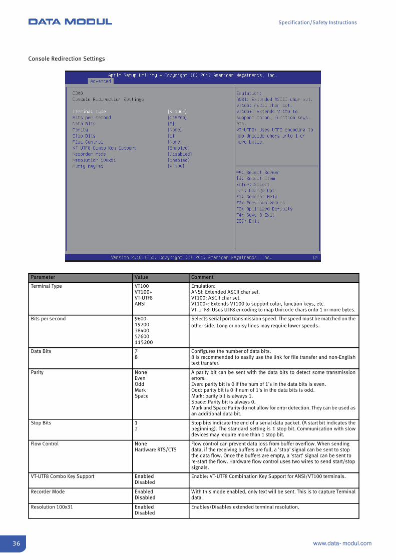
Console Redirection Settings
Parameter Value Comment
Terminal Type VT100VT100+VT-UTF8ANSI
Emulation:ANSI: Extended ASCII char set.VT100: ASCII char set.VT100+: Extends VT100 to support color, function keys, etc.VT-UTF8: Uses UTF8 encoding to map Unicode chars onto 1 or more bytes.
Bits per second 9600192003840057600115200
Selects serial port transmission speed. The speed must be matched on theother side. Long or noisy lines may require lower speeds.
Data Bits 78
Configures the number of data bits.8 is recommended to easily use the link for file transfer and non-Englishtext transfer.
Parity NoneEvenOddMarkSpace
A parity bit can be sent with the data bits to detect some transmissionerrors.Even: parity bit is 0 if the num of 1's in the data bits is even.Odd: parity bit is 0 if num of 1's in the data bits is odd.Mark: parity bit is always 1.Space: Parity bit is always 0.Mark and Space Parity do not allow for error detection. They can be used asan additional data bit.
Stop Bits 12
Stop bits indicate the end of a serial data packet. (A start bit indicates thebeginning). The standard setting is 1 stop bit. Communication with slowdevices may require more than 1 stop bit.
Flow Control NoneHardware RTS/CTS
Flow control can prevent data loss from buffer overflow. When sendingdata, if the receiving buffers are full, a 'stop' signal can be sent to stopthe data flow. Once the buffers are empty, a 'start' signal can be sent tore-start the flow. Hardware flow control uses two wires to send start/stopsignals.
VT-UTF8 Combo Key Support EnabledDisabled
Enable: VT-UTF8 Combination Key Support for ANSI/VT100 terminals.
Recorder Mode EnabledDisabled
With this mode enabled, only text will be sent. This is to capture Terminaldata.
Resolution 100x31 EnabledDisabled
Enables/Disables extended terminal resolution.
Specification/Safety Instructions
37www.data- modul.com
Parameter Value Comment
Putty KeyPad VT100LINUXXTERMR6SCOESCNVT400
Select FunctionKey and KeyPad on Putty.
Redirection After BIOS POST EnabledDisabled
Enabled: Console Redirection is available for Legacy OS.Disabled: Legacy console redirection is disabled before booting to LegacyOS.
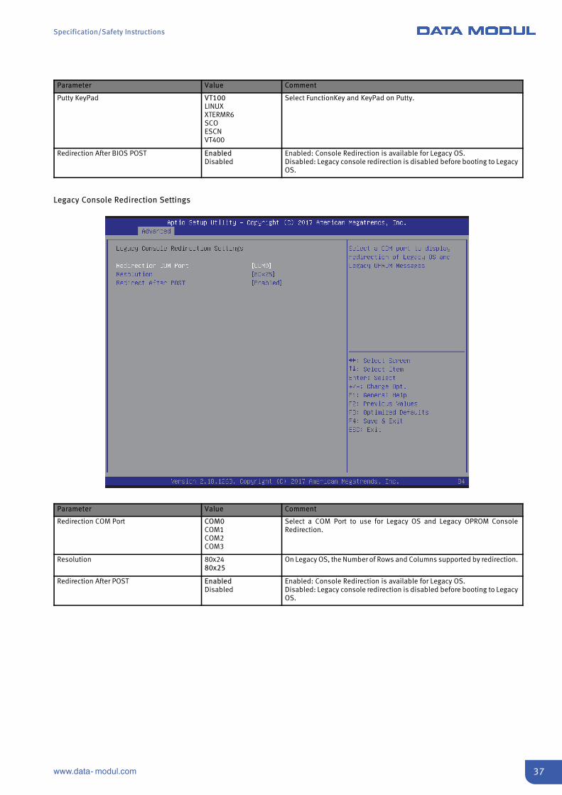
Legacy Console Redirection Settings
Parameter Value Comment
Redirection COM Port COM0COM1COM2COM3
Select a COM Port to use for Legacy OS and Legacy OPROM ConsoleRedirection.
Resolution 80x2480x25
On Legacy OS, the Number of Rows and Columns supported by redirection.
Redirection After POST EnabledDisabled
Enabled: Console Redirection is available for Legacy OS.Disabled: Legacy console redirection is disabled before booting to LegacyOS.
Specification/Safety Instructions
38 www.data- modul.com
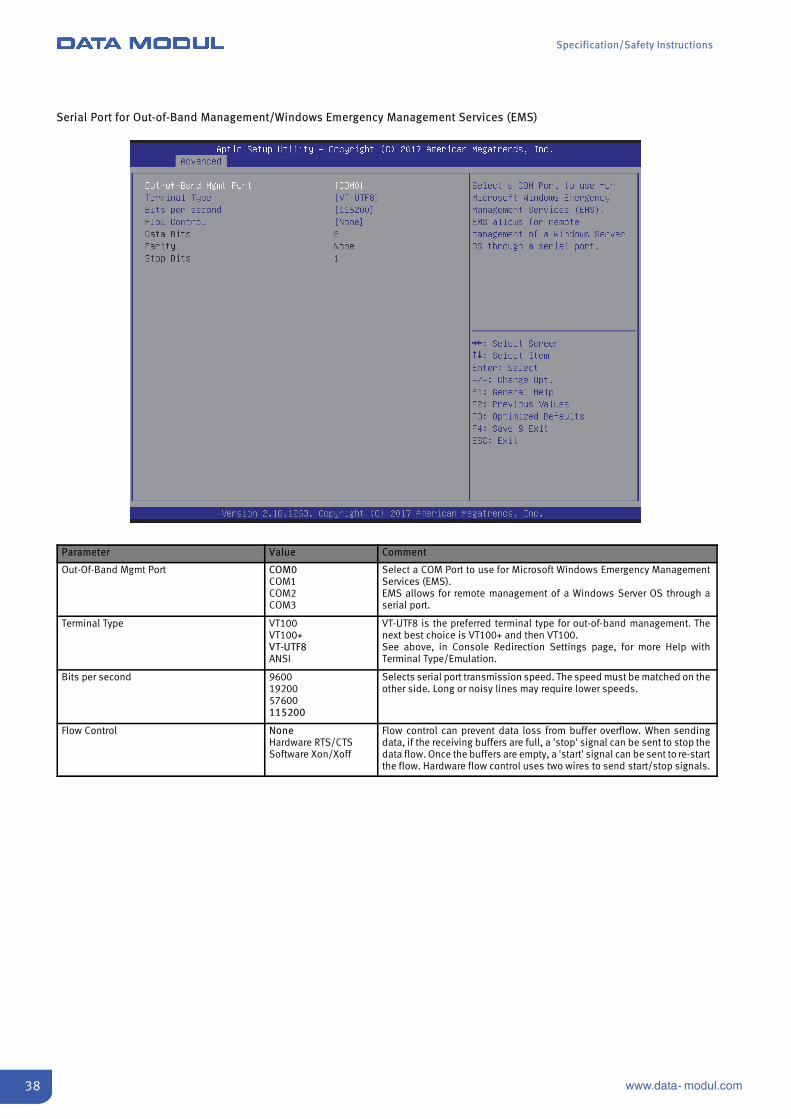
Serial Port for Out-of-Band Management/Windows Emergency Management Services (EMS)
Parameter Value Comment
Out-Of-Band Mgmt Port COM0COM1COM2COM3
Select a COM Port to use for Microsoft Windows Emergency ManagementServices (EMS).EMS allows for remote management of a Windows Server OS through aserial port.
Terminal Type VT100VT100+VT-UTF8ANSI
VT-UTF8 is the preferred terminal type for out-of-band management. Thenext best choice is VT100+ and then VT100.See above, in Console Redirection Settings page, for more Help withTerminal Type/Emulation.
Bits per second 96001920057600115200
Selects serial port transmission speed. The speed must be matched on theother side. Long or noisy lines may require lower speeds.
Flow Control NoneHardware RTS/CTSSoftware Xon/Xoff
Flow control can prevent data loss from buffer overflow. When sendingdata, if the receiving buffers are full, a 'stop' signal can be sent to stop thedata flow. Once the buffers are empty, a 'start' signal can be sent to re-startthe flow. Hardware flow control uses two wires to send start/stop signals.
Specification/Safety Instructions
39www.data- modul.com
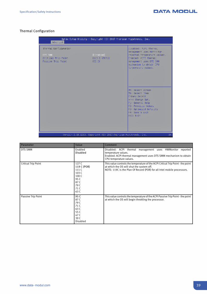
Thermal Configuration
Parameter Value Comment
DTS SMM EnabledDisabled
Disabled: ACPI thermal management uses HWMonitor reportedtemperature values.Enabled: ACPI thermal management uses DTS SMM mechanism to obtainCPU temperature values.
Critical Trip Point 127 C119 C (POR)111 C103 C100 C95 C87 C79 C71 C63 C
This value controls the temperature of the ACPI Critical Trip Point - the pointat which the OS will shut the system off.NOTE: 119C is the Plan Of Record (POR) for all Intel mobile processors.
Passive Trip Point 95 C87 C79 C71 C63 C55 C47 C39 CDisabled
This value controls the temperature of the ACPI Passive Trip Point - the pointat which the OS will begin throttling the processor.

Specification/Safety Instructions
40 www.data- modul.com
SIO Configuration
Parameter Value Comment
Serial Port 1 Submenu
View and set basic properties of the SIO logical device. Like IO base, IRQrange, DMA channel and device mode.
Serial Port 2 Submenu
Parallel Port Submenu
PS2 Controller (KB&MS) Submenu

Specification/Safety Instructions
41www.data- modul.com
Serial Port 1 Configuration
Parameter Value Comment
Use This Device EnabledDisabled
Enable or Disable this Logical Device.
Possible Use Automatic SettingsIO=3F8h; IRQ=4IO=2F8hIO=3E8hIO=2E8hIRQ=3,4,5,7,9,10,11,12
Configure Device's Resource settings. New settings will be reflectedon This Setup Page after System restarts.
Specification/Safety Instructions
42 www.data- modul.com
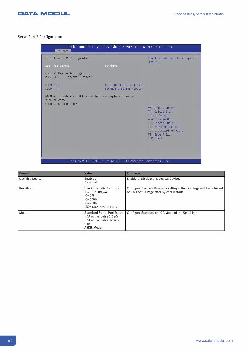
Serial Port 2 Configuration
Parameter Value Comment
Use This Device EnabledDisabled
Enable or Disable this Logical Device.
Possible Use Automatic SettingsIO=3F8h; IRQ=4IO=2F8hIO=3E8hIO=2E8hIRQ=3,4,5,7,9,10,11,12
Configure Device's Resource settings. New settings will be reflectedon This Setup Page after System restarts.
Mode Standard Serial Port ModeIrDA Active pulse 1.6 μSIrDA Active pulse 3/16 bittimeASKIR Mode
Configure Standard or IrDA Mode of the Serial Port.

Specification/Safety Instructions
43www.data- modul.com
Parallel Port Configuration
Parameter Value Comment
Use This Device EnabledDisabled
Enable or Disable this Logical Device.
Possible Use Automatic SettingsIO=378h; IRQ=5IO=278hIO=3BChIRQ=5,6,7,9,10,11,12
Configure Device's Resource settings. New settings will be reflectedon This Setup Page after System restarts.
Mode STD Printer ModeSPP ModeEPP-1.9 and SPP ModeEPP-1.7 and SPP ModeECP ModeECP and EPP 1.9 ModeECP and EPP 1.7 Mode
Change Parallel Port mode. Some of the Modes required a DMAresource. After Mode changing, Reset the System to reflect actualdevice settings.

Specification/Safety Instructions
44 www.data- modul.com
PS2 Controller (KB&MS) Configuration
Parameter Value Comment
Use This Device EnabledDisabled
Enable or Disable this Logical Device.
Possible Use Automatic SettingsIO=60h; IO=64h; IRQ=1
Configure Device's Resource settings. New settings will be reflectedon this Setup Page after System restarts.

Specification/Safety Instructions
45www.data- modul.com
Network Stack Configuration
Parameter Value Comment
Network Stack EnabledDisabled
Enable/Disable UEFI Network Stack.
Ipv4 PXE Support EnabledDisabled
Enable Ipv4 PXE Boot Support. If disabled IPV4 PXE boot option will not becreated.
Ipv4 HTTP Support EnabledDisabled
Enable Ipv4 HTTP Boot Support. If disabled IPV4 HTTP boot option will notbe created.
Ipv6 PXE Support EnabledDisabled
Enable Ipv6 PXE Boot Support. If disabled IPV6 PXE boot option will not becreated.
Ipv6 HTTP Support EnabledDisabled
Enable Ipv6 HTTP Boot Support. If disabled IPV6 HTTP boot option will notbe created.
PXE boot wait time 0 … 5 (0 default) Wait time to press ESC key to abort the PXE boot.
Media detect count 1 … 50 (1 default) Number of times presence of media will be checked.

Specification/Safety Instructions
46 www.data- modul.com
Compatibility Support Module (CSM) Configuration
Parameter Value Comment
CSM Support EnabledDisabled
Enable/Disable CSM Support.
Option ROM Messages Force BIOSKeep Current
Force BIOS: Change display to text mode and show OpROM messages.Keep Current: Don’t change display mode and suppress legacy OpROMmessages.
Boot Option Filter UEFI and LegacyLegacy onlyUEFI only
Configure available boot options.
Network Do not launchUEFILegacy
Controls the execution of UEFI and Legacy PXE OpROM.
Storage Do not launchUEFILegacy
Controls the execution of UEFI and Legacy Storage OpROM.
Video Do not launchUEFILegacy
Controls the execution of UEFI and Legacy Video OpROM.
Other PCI Devices Do not launchUEFILegacy
Determines OpROM execution policy for devices other than Network,Storage, or Video.
Specification/Safety Instructions
47www.data- modul.com
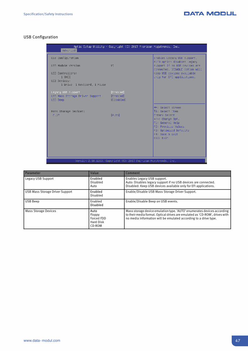
USB Configuration
Parameter Value Comment
Legacy USB Support EnabledDisabledAuto
Enables Legacy USB support.Auto: Disables legacy support if no USB devices are connected.Disabled: Keep USB devices available only for EFI applications.
USB Mass Storage Driver Support EnabledDisabled
Enable/Disable USB Mass Storage Driver Support.
USB Beep EnabledDisabled
Enable/Disable Beep on USB events.
Mass Storage Devices AutoFloppyForced FDDHard DiskCD-ROM
Mass storage device emulation type. 'AUTO' enumerates devices accordingto their media format. Optical drives are emulated as 'CD-ROM', drives withno media information will be emulated according to a drive type.

Specification/Safety Instructions
48 www.data- modul.com
Module Peripherals Configuration
Parameter Value Comment
LBAR EnabledDisabled
Configure and use Linear Base Address (LBAR) if supported in FPGA.
ACPI Devices EnabledDisabled
Select how resources are reported to the OS via ACPI.Enabled: Separate device, may require Driver.Disabled: Motherboard Resource.
UART Configuration Submenu Configure integrated UARTs.
I2C Configuration Submenu Configure integrated I2C controllers.
GPIO Bank A Configuration Submenu Configure GPIO Bank A pins.
Misc. Configuration Submenu Miscellaneous Configuration
Specification/Safety Instructions
49www.data- modul.com
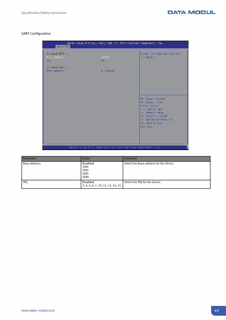
UART Configuration
Parameter Value Comment
Base Address Disabled3F8h2F8h3E8h2E8h
Select the Base address for the device.
IRQ Disabled3, 4, 5, 6, 7, 10, 11, 12, 14, 15
Select the IRQ for the device.
Specification/Safety Instructions
50 www.data- modul.com
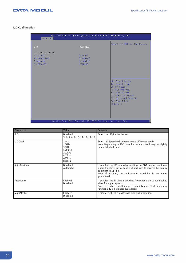
I2C Configuration
Parameter Value Comment
IRQ Disabled3, 4, 5, 6, 7, 10, 11, 12, 14, 15
Select the IRQ for the device.
I2C Clock 1kHz10kHz50kHz100kHz200kHz400kHz625kHz800kHz
Select I2C Speed (OS driver may use different speed).Note: Depending on I2C controller, actual speed may be slightlybelow selected values.
Auto-BusClear DisabledAutomatic
If enabled, the I2C controller monitors the SDA line for conditionswhere the slave device blocks it and tries to recover the bus bypulsing the SCL line.Note: If enabled, the multi-master capability is no longerguaranteed!
FastMode+ EnabledDisabled
If enabled, the SCL line is switched from open drain to push-pull toallow for higher speeds.Note: If enabled, multi-master capability and Clock stretchingfunctionality is no longer guaranteed!
MultiMaster EnabledDisabled
If disabled, the I2C master will omit bus arbitration.
Specification/Safety Instructions
51www.data- modul.com
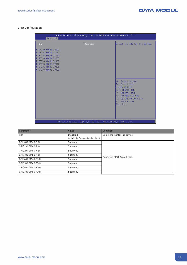
GPIO Configuration
Parameter Value Comment
IRQ Disabled3, 4, 5, 6, 7, 10, 11, 12, 14, 15
Select the IRQ for the device.
GPIO0 (COMe GPI0) Submenu
Configure GPIO Bank A pins.
GPIO1 (COMe GPI1) Submenu
GPIO2 (COMe GPI2) Submenu
GPIO3 (COMe GPI3) Submenu
GPIO4 (COMe GPO0) Submenu
GPIO5 (COMe GPO1) Submenu
GPIO6 (COMe GPO2) Submenu
GPIO7 (COMe GPO3) Submenu

Specification/Safety Instructions
52 www.data- modul.com
GPIO0 - GPIO2
Parameter Value Comment
Usage GPIO Configure GPIO usage.
Direction In (default for GPIO0-3)Out (default for GPIO5-7)
Configure GPIO direction.
Level Low-LevelHigh-Level
Configure GPIO initial level.

Specification/Safety Instructions
53www.data- modul.com
GPIO3
Parameter Value Comment
Usage GPIOUART0 DSR
Configure GPIO usage.
Direction In (default for GPIO0-3)Out (default for GPIO5-7)
Configure GPIO direction.
Level Low-LevelHigh-Level
Configure GPIO initial level.

Specification/Safety Instructions
54 www.data- modul.com
GPIO4
Parameter Value Comment
Usage GPIOPWM0UART1 CTS
Configure GPIO usage.
Direction In (default for GPIO0-3)Out (default for GPIO5-7)
Configure GPIO direction.
Level Low-LevelHigh-Level
Configure GPIO initial level.
Specification/Safety Instructions
55www.data- modul.com
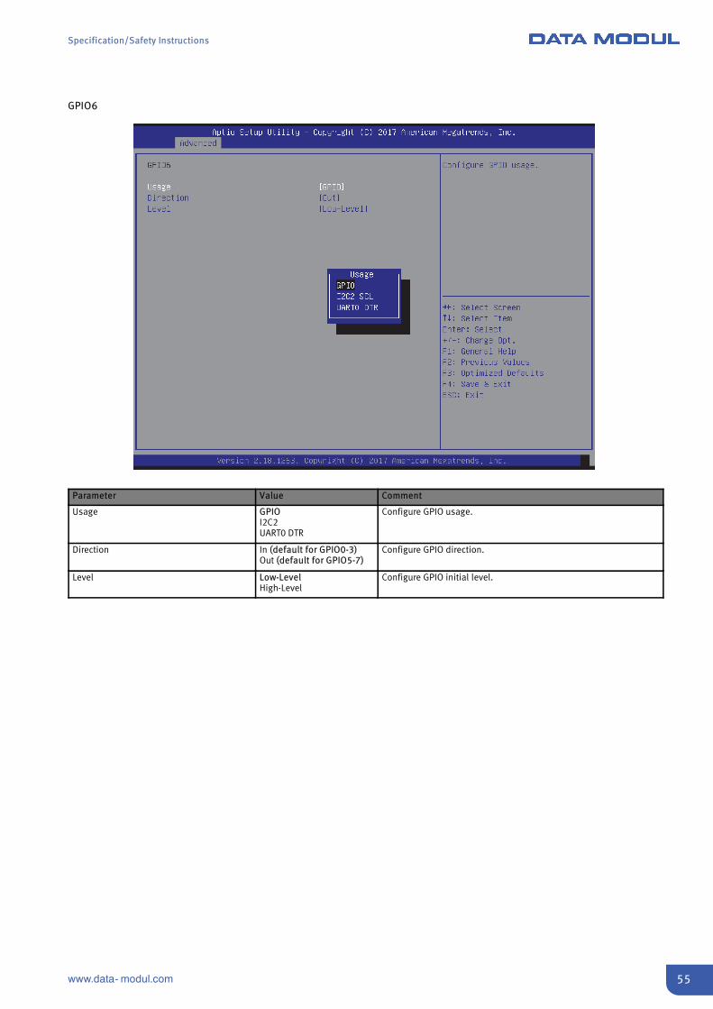
GPIO6
Parameter Value Comment
Usage GPIOI2C2UART0 DTR
Configure GPIO usage.
Direction In (default for GPIO0-3)Out (default for GPIO5-7)
Configure GPIO direction.
Level Low-LevelHigh-Level
Configure GPIO initial level.

Specification/Safety Instructions
56 www.data- modul.com
GPIO7
Parameter Value Comment
Usage GPIOI2C2 SDA
Configure GPIO usage.
Direction In (default for GPIO0-3)Out (default for GPIO5-7)
Configure GPIO direction.
Level Low-LevelHigh-Level
Configure GPIO initial level.

Specification/Safety Instructions
57www.data- modul.com
Misc. Configuration
Parameter Value Comment
Watchdog IRQ Disabled3, 4, 5, 6, 7, 10, 11,12, 14, 15
Select the IRQ for the Watchdog device. IRQ selection will be available inthe Watchdog menu after reboot.
Specification/Safety Instructions
58 www.data- modul.com
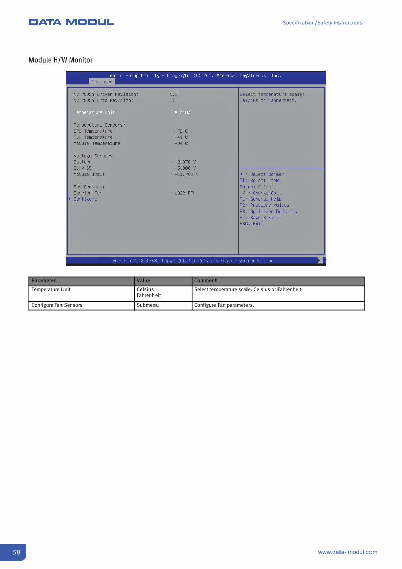
Module H/W Monitor
Parameter Value Comment
Temperature Unit CelsiusFahrenheit
Select temperature scale: Celsius or Fahrenheit.
Configure Fan Sensors Submenu Configure Fan parameters.
Specification/Safety Instructions
59www.data- modul.com
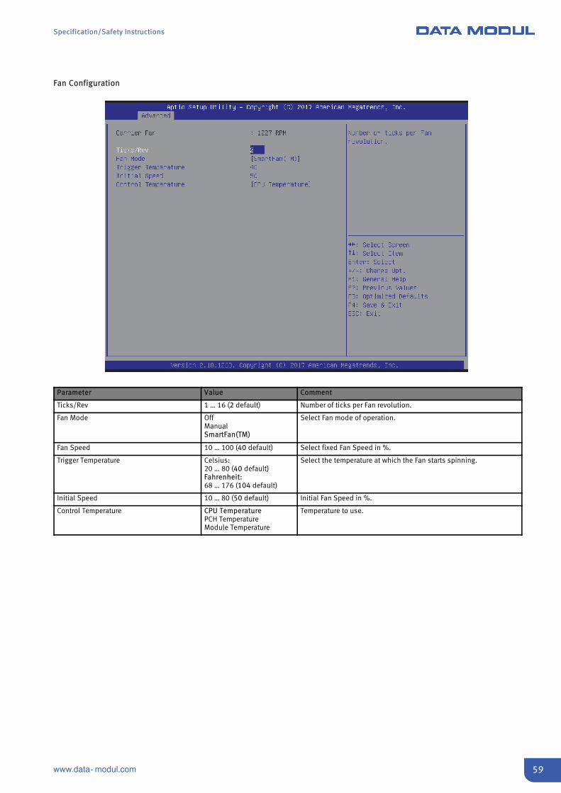
Fan Configuration
Parameter Value Comment
Ticks/Rev 1 … 16 (2 default) Number of ticks per Fan revolution.
Fan Mode OffManualSmartFan(TM)
Select Fan mode of operation.
Fan Speed 10 … 100 (40 default) Select fixed Fan Speed in %.
Trigger Temperature Celsius:20 … 80 (40 default)Fahrenheit:68 … 176 (104 default)
Select the temperature at which the Fan starts spinning.
Initial Speed 10 … 80 (50 default) Initial Fan Speed in %.
Control Temperature CPU TemperaturePCH TemperatureModule Temperature
Temperature to use.

Specification/Safety Instructions
60 www.data- modul.com
Module Watchdog Configuration
Standard Mode
Parameter Value Comment
Watchdog DisabledStandard ModeWindow Mode
Enable/Disable Watchdog and select Mode.
Auto Reload EnabledDisabled
Enable Auto Reload. If enabled, Timeout registers will be reloadedautomatically after expiration.
Lock EnabledDisabled
If enabled, the Watchdog registers will be locked and become read onlyafter initialization.
Stage Submenu Configure Watchdog Stage.

Specification/Safety Instructions
61www.data- modul.com
Stage Configuration
Parameter Value Comment
Stage Action DisabledDelayNoneResetNMIIRQ
Select Stage Action on timeout.For choosing IRQ, enable Interrupt within Menu ‘Module PeripheralsConfiguration’ – ‘Misc. Configuration’ – Watchdog IRQ’ first, then Save andReboot to Setup.
Timeout 1 … 65535 (1 default) Select the timeout value for the stage.
WDT# EnabledDisabled
Assert WDT# signal to Baseboard.
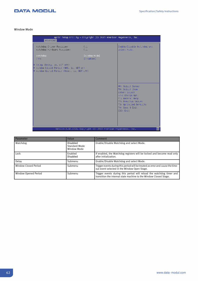
Specification/Safety Instructions
62 www.data- modul.com
Window Mode
Parameter Value Comment
Watchdog DisabledStandard ModeWindow Mode
Enable/Disable Watchdog and select Mode.
Lock EnabledDisabled
If enabled, the Watchdog registers will be locked and become read onlyafter initialization.
Delay Submenu Enable/Disable Watchdog and select Mode.
Window Closed Period Submenu Trigger events during this period will be treated as error and cause the time-out event selected in the Window Open Stage.
Window Opened Period Submenu Trigger events during this period will reload the watchdog timer andtransition the internal state machine to the Window Closed Stage.
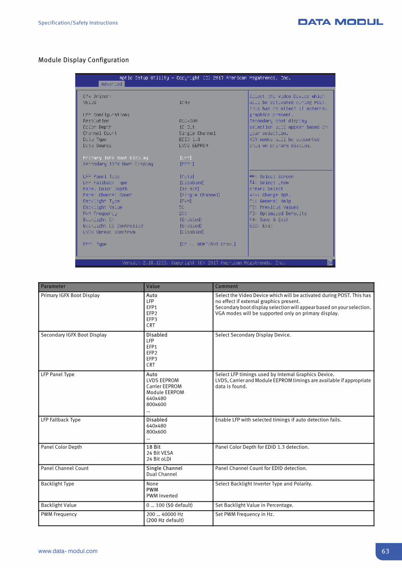
Specification/Safety Instructions
63www.data- modul.com
Module Display Configuration
Parameter Value Comment
Primary IGFX Boot Display AutoLFPEFP1EFP2EFP3CRT
Select the Video Device which will be activated during POST. This hasno effect if external graphics present.Secondary boot display selection will appear based on your selection.VGA modes will be supported only on primary display.
Secondary IGFX Boot Display DisabledLFPEFP1EFP2EFP3CRT
Select Secondary Display Device.
LFP Panel Type AutoLVDS EEPROMCarrier EEPROMModule EERPOM640x480800x600…
Select LFP timings used by Internal Graphics Device.LVDS, Carrier and Module EEPROM timings are available if appropriatedata is found.
LFP Fallback Type Disabled640x480800x600…
Enable LFP with selected timings if auto detection fails.
Panel Color Depth 18 Bit24 Bit VESA24 Bit oLDI
Panel Color Depth for EDID 1.3 detection.
Panel Channel Count Single ChannelDual Channel
Panel Channel Count for EDID detection.
Backlight Type NonePWMPWM Inverted
Select Backlight Inverter Type and Polarity.
Backlight Value 0 … 100 (50 default) Set Backlight Value in Percentage.
PWM Frequency 200 … 40000 Hz(200 Hz default)
Set PWM Frequency in Hz.
Specification/Safety Instructions
64 www.data- modul.com
Parameter Value Comment
Backlight On EnabledAt the End of Post
Configure if LVDS Backlight should be set when panel is powered, orinhibit until End Of Post.
Backlight OS Controlled EnabledDisabled
Configure if PWM values can be overridden by OS Power Options.
LVDS Spread Spectrum Disabled0.5 %1.0 %1.5 %2.0 %2.5 %
Set LVDS Center Spreading.
EFP Type HDMI/DVIDP w. HDMI/DVI Comp.DP only
Select the type of the EFP.

Specification/Safety Instructions
65www.data- modul.com
Chipset
Parameter Value Comment
System Agent (SA) Configuration Submenu System Agent (SA)Parameters (Graphics,Graphics Audio,DMI, PEG,Memory)
PCH-IO Configuration Submenu Platform Controller Hub Parameters

Specification/Safety Instructions
66 www.data- modul.com
System Agent Configuration
Parameter Value Comment
Memory Configuration Submenu Configure Memory Settings.
Graphics Configuration Submenu Configure Graphics Settings.
PEG Port Configuration Submenu Configure System Agent PCI Express Settings.
VT-d EnabledDisabled
Enable/Disable VT-d function on System Agent.(Virtualization on Technology for Directed I/O)
Above 4GB MMIO BIOS assignment EnabledDisabled
Enable/Disable above 4GB MemoryMappedIO BIOS assignment.This is disabled automatically when Aperture Size is set to 2048MB.

Specification/Safety Instructions
67www.data- modul.com
Memory Configuration
Parameter Value Comment
Max TOLUD Dynamic1 GB1.25 GB1.5 GB1.75 GB2 GB2.25 GB2.5 GB2.75 GB3 GB3.25 GB3.5 GB
Maximum Value of TOLUD. Dynamic assignment would adjust TOLUDautomatically based on largest MMIO length of installed graphic controller.
Memory Remap EnabledDisabled
Enable/Disable memory remap above 4GB.
MRC Fast Boot EnabledDisabled
Enable/Disable MRC fast boot. Skips memory training if memoryconfiguration not changed.

Specification/Safety Instructions
68 www.data- modul.com
Graphics Configuration
Parameter Value Comment
Skip Scanning of External Gfx Card EnabledDisabled
Enabled/Disable scanning of External Gfx Card on PEG and PCH PCIe Ports.
Primary Display AutoIGFXPEGPCIe
Select which of IGFX/PEG/PCIe Graphics Device should be Primary Display.
Internal Graphics AutoDisabledEnabled
Keep IGFX enabled based on the setup options.
Aperture Size 128MB … 2048MB(256MB default)
Select the Aperture Size.Note: Above 4GB MMIO BIOS assignment is automatically enabled whenselecting 2048MB aperture. To use this feature, please disable CSMSupport.
DVMT Pre-Allocated 0MB … 64MB(32MB default)
Select DVMT (Dynamic Video Memory Technology)5.0 Pre-Allocated (Fixed)Graphics Memory size used by the Internal Graphics Device.
DVMT Total Gfx Mem 128MB256MBMAX
Select DVMT5.0 Total Graphic Memory size used by the Internal GraphicsDevice.
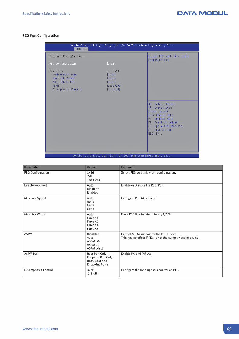
Specification/Safety Instructions
69www.data- modul.com
PEG Port Configuration
Parameter Value Comment
PEG Configuration 1x162x81x8 + 2x4
Select PEG port link width configuration.
Enable Root Port AutoDisabledEnabled
Enable or Disable the Root Port.
Max Link Speed AutoGen1Gen2Gen3
Configure PEG Max Speed.
Max Link Width AutoForce X1Force X2Force X4Force X8
Force PEG link to retrain to X1/2/4/8.
ASPM DisabledAutoASPM L0sASPM L1ASPM L0sL1
Control ASPM support for the PEG Device.This has no effect if PEG is not the currently active device.
ASPM L0s Root Port OnlyEndpoint Port OnlyBoth Root andEndpoint Ports
Enable PCIe ASPM L0s.
De-emphasis Control -6 dB-3.5 dB
Configure the De-emphasis control on PEG.
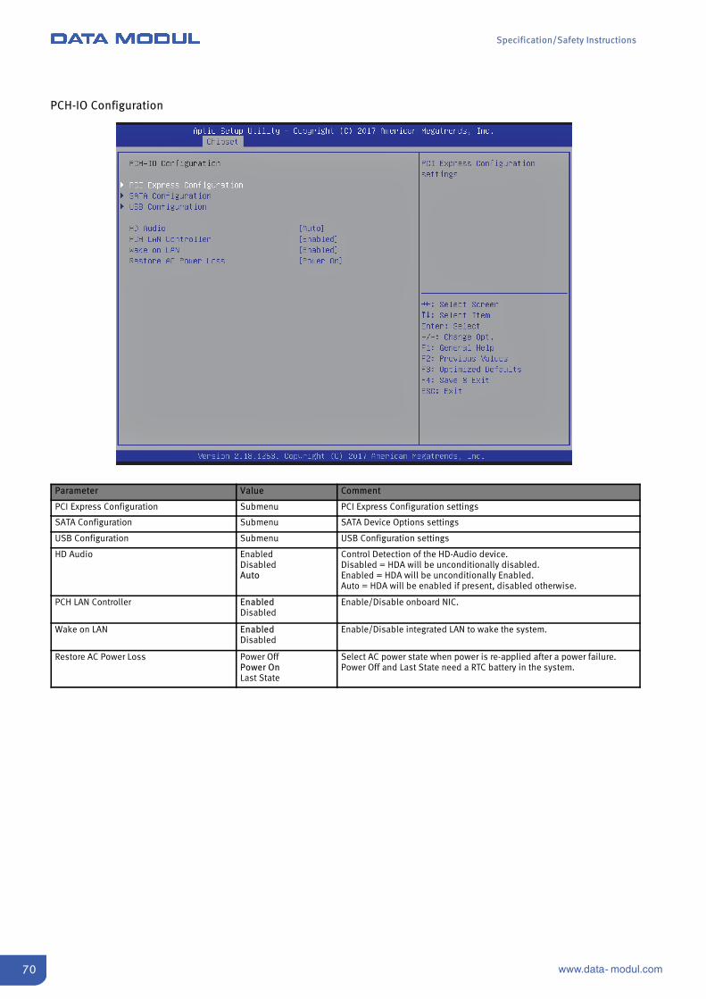
Specification/Safety Instructions
70 www.data- modul.com
PCH-IO Configuration
Parameter Value Comment
PCI Express Configuration Submenu PCI Express Configuration settings
SATA Configuration Submenu SATA Device Options settings
USB Configuration Submenu USB Configuration settings
HD Audio EnabledDisabledAuto
Control Detection of the HD-Audio device.Disabled = HDA will be unconditionally disabled.Enabled = HDA will be unconditionally Enabled.Auto = HDA will be enabled if present, disabled otherwise.
PCH LAN Controller EnabledDisabled
Enable/Disable onboard NIC.
Wake on LAN EnabledDisabled
Enable/Disable integrated LAN to wake the system.
Restore AC Power Loss Power OffPower OnLast State
Select AC power state when power is re-applied after a power failure.Power Off and Last State need a RTC battery in the system.
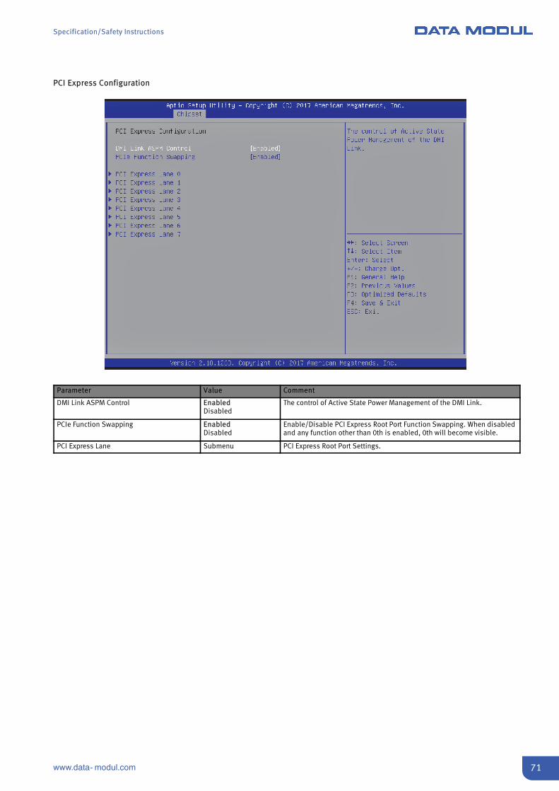
Specification/Safety Instructions
71www.data- modul.com
PCI Express Configuration
Parameter Value Comment
DMI Link ASPM Control EnabledDisabled
The control of Active State Power Management of the DMI Link.
PCIe Function Swapping EnabledDisabled
Enable/Disable PCI Express Root Port Function Swapping. When disabledand any function other than 0th is enabled, 0th will become visible.
PCI Express Lane Submenu PCI Express Root Port Settings.
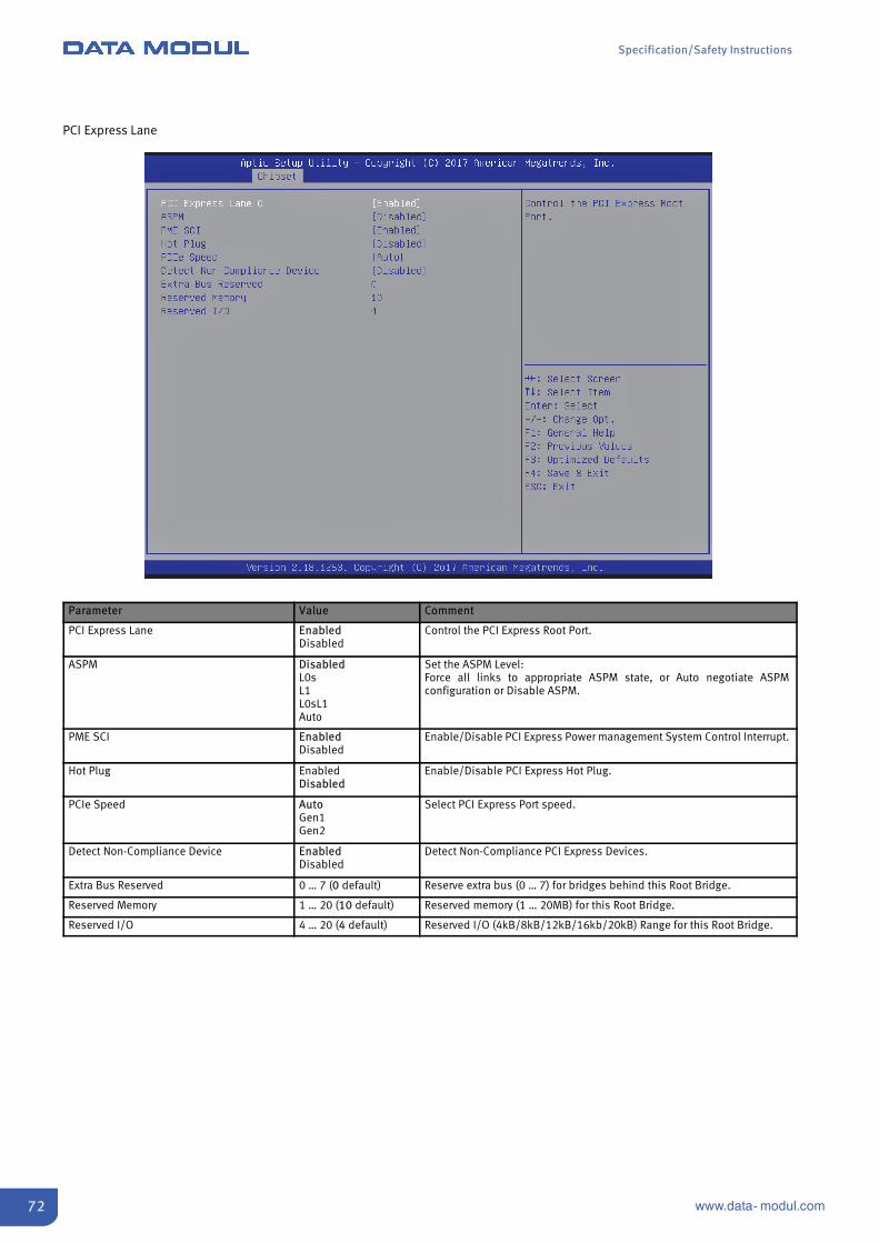
Specification/Safety Instructions
72 www.data- modul.com
PCI Express Lane
Parameter Value Comment
PCI Express Lane EnabledDisabled
Control the PCI Express Root Port.
ASPM DisabledL0sL1L0sL1Auto
Set the ASPM Level:Force all links to appropriate ASPM state, or Auto negotiate ASPMconfiguration or Disable ASPM.
PME SCI EnabledDisabled
Enable/Disable PCI Express Power management System Control Interrupt.
Hot Plug EnabledDisabled
Enable/Disable PCI Express Hot Plug.
PCIe Speed AutoGen1Gen2
Select PCI Express Port speed.
Detect Non-Compliance Device EnabledDisabled
Detect Non-Compliance PCI Express Devices.
Extra Bus Reserved 0 … 7 (0 default) Reserve extra bus (0 … 7) for bridges behind this Root Bridge.
Reserved Memory 1 … 20 (10 default) Reserved memory (1 … 20MB) for this Root Bridge.
Reserved I/O 4 … 20 (4 default) Reserved I/O (4kB/8kB/12kB/16kb/20kB) Range for this Root Bridge.

Specification/Safety Instructions
73www.data- modul.com
SATA Configuration
Parameter Value Comment
SATA Controller EnabledDisabled
Enable/Disable SATA Device.
SATA Mode Selection AHCIIntel RST
Determines how SATA controller operate.
Aggressive LPM Support EnabledDisabled
Enable PCH to aggressively enter link power state.
SATA Controller Speed DefaultGen1Gen2Gen3
Default configures controller speed to max supported speed of connecteddevices.Other values limit speed to according value.Gen1: 1GB/s, Gen2: 3Gb/s, Gen3: 6Hb/s
Software Feature Mask Configuration Submenu Configure RAID and Smart Response Technology features.
SATA Port EnabledDisabled
Enable/Disable SATA Port.
Hot Plug EnabledDisabled
Designates this port as Hot Pluggable.

Specification/Safety Instructions
74 www.data- modul.com
Software Feature Mask Configuration
Parameter Value Comment
RAID0 EnabledDisabled
Enable/Disable RAID0 feature.
RAID1 EnabledDisabled
Enable/Disable RAID1 feature.
RAID10 EnabledDisabled
Enable/Disable RAID10 feature.
RAID5 EnabledDisabled
Enable/Disable RAID5 feature.
OPROM Interface EnabledDisabled
If enabled, the OPROM User Interface is shown. Otherwise, no OPROMbanner or information will be displayed if all disks and RAID volumes arenormal.
OPROM Interface Delay 2 Seconds4 Seconds6 Seconds8 Seconds
Select the delay time of the OPROM Splash Screen in a normal status.
Smart Response Technology EnabledDisabled
Enable/Disable Smart Response Technology.

Specification/Safety Instructions
75www.data- modul.com
USB Configuration
Parameter Value Comment
USB Per-Port Disable EnabledDisabled
Enable/Disable the corresponding USB port from reporting a DeviceConnection to the controller.If all ports are disabled, setup cannot be entered anymore with USBkeyboard.
USB Port EnabledDisabled
Enable/Disable USB Port.

Specification/Safety Instructions
76 www.data- modul.com
Security
Parameter Value Comment
Administrator Password Set Administrator Password.
User Password Set User Password.
User Password Policy SetupBootBoot + Setup
Setup: Password is necessary to enter Setup.Boot: Password is needed for starting system. If Administrator Password isalso active, Setup can only be entered with Administrator Password.Boot+Setup: Password needed during POST, enter setup with UserPassword possible.
HDD Security Submenu HDD Security Configuration for selected drive.
Secure Boot Submenu Customizable Secure Boot settings
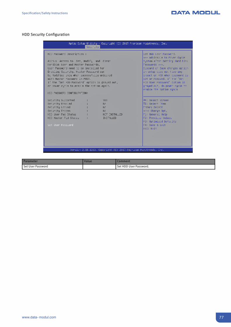
Specification/Safety Instructions
77www.data- modul.com
HDD Security Configuration
Parameter Value Comment
Set User Password Set HDD User Password.

Specification/Safety Instructions
78 www.data- modul.com
Secure Boot Configuration
Parameter Value Comment
Secure Boot EnabledDisabled
Secure Boot can be enabled if:1. System running in User mode with enrolled Platform Key(PK).2. CSM function is disabled.
Secure Boot Mode StandardCustom
Secure Boot mode selector:In Custom mode Secure Boot Variables can be configured withoutauthentication.
Key Management Submenu Enables expert users to modify Secure Boot Policy variables without fullauthentication.
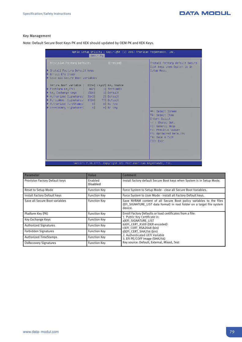
Specification/Safety Instructions
79www.data- modul.com
Key Management
Note: Default Secure Boot Keys PK and KEK should updated by OEM PK and KEK Keys.
Parameter Value Comment
Provision Factory Default keys EnabledDisabled
Install factory default Secure Boot keys when System is in Setup Mode.
Reset to Setup Mode Function Key Force System to Setup Mode - clear all Secure Boot Variables.
Install Factory Default keys Function Key Force System to User Mode - install all Factory Default keys.
Save all Secure Boot variables Function Key Save NVRAM content of all Secure Boot policy variables to the files(EFI_SIGNATURE_LIST data format) in root folder on a target file systemdevice.
Platform Key (PK) Function Key Enroll Factory Defaults or load certificates from a file:1. Public Key Certificate in:a)EFI_SIGNATURE_LISTb)EFI_CERT_X509 (DER encoded)c)EFI_CERT_RSA2048 (bin)d)EFI_CERT_SHA256 (bin)2. Authenticated UEFI Variable3. EFI PE/COFF Image (SHA256)Key source: Default, External, Mixed, Test
Key Exchange Keys Function Key
Authorized Signatures Function Key
Forbidden Signatures Function Key
Authorized TimeStamps Function Key
OsRecovery Signatures Function Key

Specification/Safety Instructions
80 www.data- modul.com
Boot
Device Based
Parameter Value Comment
Setup Prompt Timeout 1 … 65535 (1 default) Number of seconds to wait for setup activation key. 65535(0xFFFF) meansindefinite waiting.
Bootup NumLock State OnOff
Select the keyboard NumLock state.
Popup Boot Menu EnabledDisabled
Enable/Disable Popup Boot Menu.
Quiet Boot EnabledDisabled
Enables or Disables Quiet Boot option.
Fast Boot EnabledDisabled
Enables/Disables boot with initialization of a minimal set of devicesrequired to launch active boot option.
SATA Support Last Boot HDD OnlyAll Sata Devices
Select if only last HDD booted or all SATA HDD should be initialized.
VGA Support AutoEFI Driver
If Auto, only install Legacy OpROM with Legacy OS. Logo would NOT beshown during post.Efi driver will still be installed with EFI OS.
USB Support DisabledFull InitialPartial Initial
If Disabled, all USB devices will NOT be available until OS boot.If Partial Initial, USB Mass Storage and specific USB port/device will NOTbe available before OS boot.If Enabled, all USB devices will be available in OS and Post.
PS2 Device Support EnabledDisabled
If Disabled, PS2 devices will be skipped.
Network Stack Driver Support EnabledDisabled
If Disabled, Network Stack Driver will be skipped.
Redirection Support EnabledDisabled
If Disabled, Redirection function will be disabled.
New Boot Option Policy DefaultPlace FirstPlace Last
Controls the placement of newly detected UEFI boot options.
Boot Menu Mode Device BasedPort Based
Device: Choose Boot Option by Device,Port: Choose Boot Option by Type.Need to reset and enter setup again for changes.

Specification/Safety Instructions
81www.data- modul.com
Parameter Value Comment
Boot Option Priorities Depends onrecognized devise
Sets the boot order.Priority of devices from same type can be selected in BBS priority menus.
Hard Drive BBS Priorities Submenu Set the order of the legacy devices in this group.Content depend on recognized devices.
USB Device BBS Priorities Submenu Set the order of the legacy devices in this group.Content depend on recognized devices.
Port Based
Parameter Value Comment
USB Boot Devices GroupedBy Port
Show all USB Boot Devices in one group or show all USB Ports.
Boot Option Priorities Depends onrecognized device
Sets the boot order.Priority of devices from same type can be selected in Priority Submenus.
USB Priorities Submenu Set the order of the devices in this group.Content depend on recognized devices.

Specification/Safety Instructions
82 www.data- modul.com
Save & Exit
Parameter Value Comment
Save Changes and Exit Function Key Exit system setup after saving the changes.
Discard Changes and Exit Function Key Exit system setup without saving any changes.
Save Changes and Reset Function Key Reset the system after saving the changes.
Discard Changes and Reset Function Key Reset system setup without saving any changes.
Save Changes Function Key Save Changes done so far to any of the setup options.
Discard Changes Function Key Discard Changes done so far to any of the setup options.
Restore Defaults Function Key Restore/Load Default values for all the setup options.
Save as User Defaults Function Key Save the changes done so far as User Defaults.
Restore User Defaults Function Key Restore the User Defaults to all the setup options.
Boot Override Depends onrecognized devise
Boots to selected device.
Launch EFI Shell from filesystem device Function Key Attempts to Launch EFI Shell application (Shell.efi) from one of theavailable filesystem devices.

Specification/Safety Instructions
83www.data- modul.com
This page intentionally left blank.
Headquarters:
DATA MODUL AG Landsberger Str. 322 DE-80687 Munich - Germany Phone: +49-89-56017-0 Fax: +49-89-56017-119 www.data-modul.com
Logistics, Production & Services:
DATA MODUL Weikersheim GmbH Lindenstrasse 8 DE-97990 Weikersheim - Germany Phone: +49-7934-101-0 Fax: +49-7934-101-101
Subsidiaries & Sales Offices:
Germany – HamburgGermany – DuesseldorfDenmarkDubaiFinland/BalticFranceItalySingaporeSpainSwitzerlandUKUSA
DATA MODUL’s worldwide offices can be found on our website:www.data-modul.com/eu/sm/contact-us/offices.html
10
.20
13
DIN-EN-ISO 9001/14001 | www.data-modul.com