
edge.rit.eduedge.rit.edu/content/P10022/public/team_docs/P10022... · Web viewScale value to...
63
P10022 Transcutaneous Signal Transmission for LVAD November 6, 2009 Sara Carr Robert MacGregor Carl Hoge Keith Lesser Oxana Petritchenko
Transcript of edge.rit.eduedge.rit.edu/content/P10022/public/team_docs/P10022... · Web viewScale value to...

P10022
Transcutaneous Signal Transmission for LVADNovember 6, 2009
Sara Carr
Robert MacGregor
Carl Hoge
Keith Lesser
Oxana Petritchenko

KGCOE MSD I Detailed Design Review: 11/6/2009P10022: Transcutaneous Signal Transmission for LVAD Guides: Dr. Day, Dr. Lux
Table of Contents
Detailed Design Review Agenda...............................................................................................3
High-Level Project Summary......................................................................................................4
Project Background:................................................................................................................4
Problem Statement:.................................................................................................................4
Objectives/Scope:....................................................................................................................4
Deliverables:.............................................................................................................................4
Expected Project Benefits:......................................................................................................4
Core Team Members:.............................................................................................................4
Strategy & Approach...................................................................................................................5
Assumptions & Constraints:...................................................................................................5
Issues & Risks:.........................................................................................................................5
Customer Needs..........................................................................................................................6
Customer Specifications.............................................................................................................7
High-Level Design Schematics..................................................................................................8
Schematic #1: Current Design...............................................................................................8
Schematic #2: Proposed Design............................................................................................9
Schematic #3: Big Picture Design.......................................................................................10
Electronics Design.....................................................................................................................11
Interior Circuit Schematic......................................................................................................11
Exterior Circuit Schematic.....................................................................................................12
Micro Controller......................................................................................................................13
Digital to Analog Converter...................................................................................................15
Clock Oscillator HCMOS/TTL CTS Model 632..................................................................16
Pseudocode................................................................................................................................17
Wireless Power Transfer...........................................................................................................22
DC/AC Inverter.......................................................................................................................22
AC/DC Rectifier......................................................................................................................25
Charging Circuit......................................................................................................................27
Design of Coils.......................................................................................................................28
Page 1 of 53

KGCOE MSD I Detailed Design Review: 11/6/2009P10022: Transcutaneous Signal Transmission for LVAD Guides: Dr. Day, Dr. Lux
Potential Packaging of Coils.................................................................................................29
Interior and Exterior Casing Design........................................................................................30
Heat Shrink Boots..................................................................................................................32
O-ring Cord.............................................................................................................................33
O-rings.....................................................................................................................................33
Mechanical Damping Grommets..........................................................................................34
Screws.....................................................................................................................................34
Alden Connector.......................................................................................................................36
Heat Transfer Analysis..............................................................................................................37
Wire and Cable Selection.........................................................................................................39
Proposed Wire Design #1: One Wire..................................................................................40
Proposed Wire Design #2: Two Separate Wires...............................................................40
Wire Shielding........................................................................................................................41
Noise Reduction.................................................................................................................41
Shielding..............................................................................................................................41
Bill of Materials...........................................................................................................................42
Test Plans...................................................................................................................................44
LVAD Simulation Signal Test...............................................................................................44
Wireless Power Transfer Test..............................................................................................45
Electronics Functionality Test...............................................................................................46
Current System Test..........................................................................................................47
P10021 Senior Design Team Project Test.....................................................................47
Flexibility Test.........................................................................................................................48
Alternative Method:............................................................................................................49
Heat Test.................................................................................................................................50
Drop Test................................................................................................................................51
Pressure and Leak Test........................................................................................................52
Risk Assessment........................................................................................................................53
Page 2 of 53

KGCOE MSD I Detailed Design Review: 11/6/2009P10022: Transcutaneous Signal Transmission for LVAD Guides: Dr. Day, Dr. Lux
Page 3 of 53

KGCOE MSD I Detailed Design Review: 11/6/2009P10022: Transcutaneous Signal Transmission for LVAD Guides: Dr. Day, Dr. Lux
Detailed Design Review AgendaMeeting Purpose:
1. Overview of the project
2. Present the design concepts
3. Confirm the design functionality
4. Confirm materials and components needed for design
Materials to be Reviewed:
1. Project Description: Customer Needs and Specifications
2. Electronics Design
3. Pseudocode
4. Wireless Power Transfer
5. Interior and Exterior Casing
6. Bill of Materials
7. Test Plans
Meeting Date: 11/6/09
Meeting Location: 09-4425
Meeting time: 11:00 – 1:00 pm
Meeting TimelineStart time Topic of Review Required Attendees
11:00 Project Overview Dr. Day,Dr .Lux,Dr.
Cheng, Dr. Tsouri11:05 Electronics Overview Dr. Day,Dr .Lux,Dr.
Cheng, Dr. Tsouri11:25 Pseudocode Dr. Day,Dr .Lux,Dr.
Cheng11:40 Wireless Power Transfer Dr. Day,Dr .Lux,Dr.
Cheng11:55 Casing Dr. Day,Dr .Lux,Dr.
Cheng12:15 Bill Of Materials Dr. Day,Dr .Lux,Dr.
Cheng12:35 Test Plans Dr. Day,Dr .Lux,Dr.
Cheng12:45 Questions, Concerns, Ideas, Review Dr. Day,Dr .Lux,Dr.
Cheng
Page 4 of 53

KGCOE MSD I Detailed Design Review: 11/6/2009P10022: Transcutaneous Signal Transmission for LVAD Guides: Dr. Day, Dr. Lux
High-Level Project Summary
Project Background: A Ventricular assist device, or VAD, is a mechanical device that is used to partially replace the function of a failing heart. Some VADs are intended for short term use, typically for patients recovering from heart attacks or heart surgery, while others are intended for long term use, typically for patients suffering from congestive heart failure. Long term VADs are normally used to keep patients alive with a good quality of life while they wait for a heart transplant. The first versions of the RIT LVAD blood pump used a large cable through the skin to transmit all power and control signals. The lack of flexibility in this cable caused discomfort, limited range of motion and infection.
Problem Statement: Eliminate as many wires as possible going through the dermis of the patient from the exterior electronics to the Left Ventricular Assist Device (LVAD) blood pump. This can be achieved using wireless technology or by other design means of eliminating unnecessary wires.
Objectives/Scope:1. Improve flexibility of cable by eliminating redundant wires.2. Ensure functions of the LVAD are not impaired.3. Ensure safety of implanting the casing for
internal components.
4. Wireless power transmission is optional.
Deliverables: Improved signal transmission that meets customer needs New design, sketches, mechanical and electrical drawings Documented signal transmission data A functioning prototype
Expected Project Benefits:The current design uses 23 wires leading from the control unit to the LVAD blood pump, entering through
the skin and into the body of the patient. The design is associated with many health risks to the patient because the exposure of the tissue to the cable causes many infections which often lead to death of the patient. Our project benefits the patient by eliminating all but four of the wires leading to the LVAD heart pump, therefore, reducing the size of the cable, and therefore the chance of infection.
Core Team Members: Carl Hoge Keith Lesser Oxana Petritchenko – Project Manager Robert MacGregor Sara Carr – Lead Engineer
Page 5 of 53

KGCOE MSD I Detailed Design Review: 11/6/2009P10022: Transcutaneous Signal Transmission for LVAD Guides: Dr. Day, Dr. Lux
Strategy & Approach
Assumptions & Constraints: The team must obtain a well rounded understanding of the current heart pump system in order to determine which signals must be transmitted. The team must assume that certain electronics may be placed inside the body in order to eliminate larger wires passing through the skin. The ability to transmit certain signals may be a constraint on the team’s ability to eliminate wires or to use smaller wires. The team will focus on design issues throughout the duration of the project in order to assist in the development of future design iterations.
Issues & Risks: Difficulty of signal transmission and reception. Obtaining parts and hardware that can be implemented with current system. Health risks associated with tissue damage by packaging of electronics and heat generated by
them.
Page 6 of 53

Customer Needs

Customer Specifications

High-Level Design Schematics
Schematic #1: Current Design

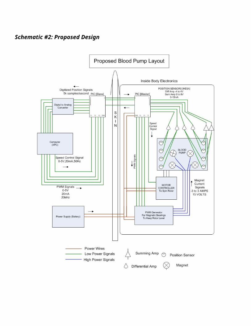
Schematic #2: Proposed Design
Schematic #3: Big Picture Design

Electronics Design
The communication between each end of the cable is provided by two MicroChip dsPic33FJ32GP304. One transceiver is implanted inside the body and connects to the P10021 project by a 27 pin connector. Three wire Serial Peripheral Interface (SPI) is used to transmit the LVAD data to the exterior controller at frequency up to 40MHz. The voltages from HESA position monitors are shifted to the tolerance of the microcontroller using a voltage shifter. A voltage shifter is a simple circuit that uses resistors to change the potential of the signal, but is scaled in a way that can regenerate the original signals. A 5V to 3.3V voltage regulator is used to deliver a voltage source to the microprocessor; since the processor draws varying amounts of current a resistor network was not sufficient for this voltage source. These position signals are sampled by the dsPIC33F using the built in 12 bit analog to digital converter. Once digitized these signals are sent along the SPI interface. The PWM duty cycles are received on the SPI interface and sampled on the dsPIC33F and sent to the 27 pin connector to project P10021 at a rate of up to 20Mbps.
Interior Circuit Schematic

Exterior Circuit Schematic In order to integrate fully with project P10021, the position signals must be delivered as analog signals
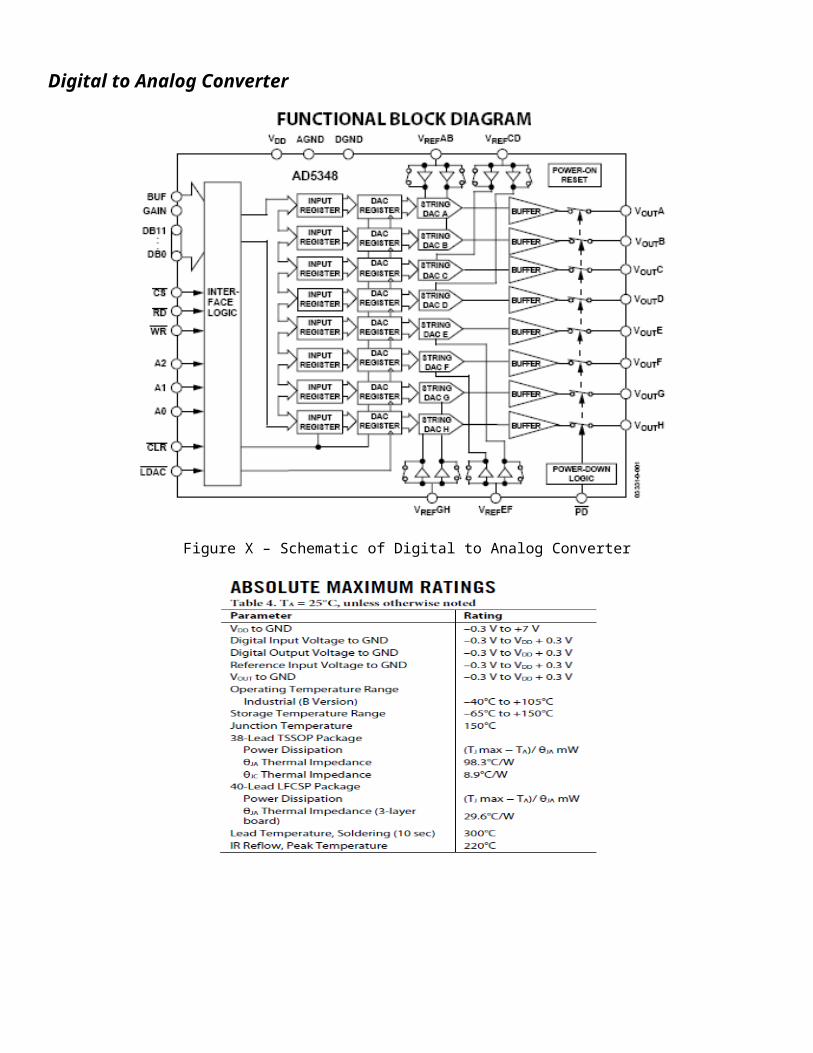
instead of digital. Therefore, an 8-channel digital to analog converter (DAC) is utilized. The DAC takes in 12 bits at a time in a parallel interface and samples them at 125ksps. The microcontroller of project P10021 samples the position signals a 5 kHz, therefore 125ksps is a suitable speed for this application. A functional block diagram is pictured below.
In order to avoid possible errors in pin connections and to easily troubleshoot, an Excel spread sheet is kept to map each pin to each chip.
STARTS ENDSPIN VALUE I/O PIN VALUE I/O CHIP
1 PWM1 I 13 CONN O 27 CONN2 PWM2 I 14 CONN O 27 CONN3 PWM3 I 15 CONN O 27 CONN4 PWM4 I 16 CONN O 27 CONN5 MC1 I 17 CONN O 27 CONN6 VSS P GND 7 VDDCAP P 10uF Cap 8 LDAC1 O 7 LDAC I AD53489 LDAC2 O 39 LDAC I AD5348
Table – Example of Pin Mapping Spread Sheet

Micro Controller


Digital to Analog Converter
Figure X – Schematic of Digital to Analog Converter

Clock Oscillator HCMOS/TTL CTS Model 632
Pseudocode
Theory of Operation
During concept selection, it was determined that one of the methods of serial communication would work best for our task. When determining the best method of transmission for this project, several factors had to be considered. The method should be fast, reliable, be able to communicate in both directions, use low power, be easy to implement, and use as few and as small of wires as possible. A comparison of some common serial communication methods have shown SPI to be the best suited to our needs.
Method Speed Reliability Comm Mode Ease of Imp. Availability Wires
SPI 20 Mbps Best Full Duplex Simple Widely 3
USB 480 Mbps Good Half Duplex Complex Limited 2
I2C 3 Mbps Good Half Duplex Simple Widely 2
1 Wire <1 Mbps Good Half Duplex Simple Widely 1
A quick comparison shows SPI to be our best choice. It can communicate at speeds up to 20 Mbps. This is important, because a calculation shows the need for ~16 Mbps for optimal communication:
6*12bits*5ksps = 360kbps for Position Signal Transmission
4*1bits*4MHz = 16Mbps for PWM Signal Transmission
1*1bit*5ksps = 5kbps for Motor control
Total + Overhead = ~16.5 Mbps
It has the ability to communicate in full duplex mode and should reduce communication lag. Its reliability should be very good due to the fact that it uses a clock wire, eliminating the need to have precision oscillators. It is commonly found in many microcontrollers making it easy to pick components, as opposed to USB where only certain controllers have onboard support. All methods have been around for a while and have sufficient documentation, with USB being the most complex of the four. The disadvantage of SPI is that it uses more wires, but this will hopefully be offset by the size of the wires being so small, as they will only be carrying 0-3.3V and ~5mA of current.
How the PICs will communicate will be better seen in this diagram.

Here we can see that a 3 wire system is being used to communicate between the two PICs. There is a data in, data out, and clock wire used. Data is constantly being put into the shift register, sent to the recipients shift register, where it is read into memory, and more data is put into the register to be sent out. Because there will be only two devices communicating, the slave select line can be set to high on the master and low on the slave.
In our system, the Master will be the PIC on the inside. This PIC will handle doing the A/D of the Position Signals [Hall Effect Sensor Signals], sending that information to the PIC on the outside, as well as receiving PWM information from the PIC on the outside, and sending those signals to the PWM amplifier and the motor controller.
For this project the Microchip dsPIC33FJ32GP304 was chosen for both ends. This PIC was chosen for a variety of reasons including processing power, 16-bit word size, the speed and precision of its A/D converter, wide availability, low price, and our own familiarity with the Microchip PIC line.
For each PIC separate tasks will have to be performed, and different code will be needed for each PIC. The code for these can be seen below.

Pseudocode
Master PIC (Interior)
#include dsPIC33f.h
Set up clock and set to external
Set I/O Pins – 7 Inputs [6 for Position Signals, 1 for SPI]
7 Outputs [4 PWM Signals, 1 Speed Control Signal, 2 SPI]
Set 6 Positions Input Pins to be Analog Inputs
Set ADC precision to 12 bits
Set ADC to use external clock
Set SPI to use 2 Outputs / 1 Input
Main Loop
For ADC1 -> ADC6
Get value from ADC register
Scale value to represent correct voltage
Create word-sized data containing input values
Add bits to distinguish signals from each other
Load signal into SPI Buffer
Wait until transfer is completed
Read Data from SPI Buffer into Memory
Set appropriate outputs based on received data

Pseudocode
Slave PIC (Exterior)
#include dsPIC33f.h
Set clock to external
Set I/O Pins – 7 Inputs [5 for PWM Signals, 2 for SPI]
13 Outputs [12 Parallel Outputs for DAC, 1 SPI]
Set all I/O to digital
Set SPI to use 2 Outputs / 1 Input
Main Loop
Sample all of the inputs
Create a word-sized piece of data containing input information
Load data into SPI Buffer
Wait until transfer is completed
Read Data from SPI Buffer into Memory
Break data down so it can be output in parallel
Set output pins based on data
Flowchart of the path of a Position Signal going from the Blood Pump Main Controller

Wireless Power Transfer

Through the use of inductive coupling, a voltage can be induced without a direct contact. Several heart pumps on the market are using this coupling such as the Abiocore and Thoratec. Using the following design, we hope to attain a wireless power transfer able to transmit 20 watts of power from an external battery to the internal system.
Schematic of Inductive Coupling Power Transmission System
DC/AC InverterA transformer is used to convert a direct current to an alternating current using inductive coupling. A
DC voltage is applied to the secondary coil (labeled SEC in diagram) and induces an AC voltage on the primary current. The DC to AC converter being used is a 60Hz monostable multi-vibrating circuit. The center lead of the primary coil has 15 volts applied to it, causing the BJT transistors to turn on and off. This oscillation will induce an AC voltage across the primary coil. The frequency of the oscillation is based on the resistor value R.
Example of a DC to AC Converter (by Harry Lythall)

Coil Diagram of Transformer (a) Example of Transformer (b)

Schematic of Inverter
AC/DC RectifierAn AC to DC converter, also known as a rectifier is used to deliver a direct current to the heart pump. It
takes the negative portion of an AC voltage and makes it positive. This is generally done using diodes. In order to eliminate ripples in the response, a capacitor can be added. In order to eliminate design and manufacturing time, an AC to DC converter will be purchased off the shelf. The GCS20 delivers 20W and 15V and comes in a small package, which is ideal for this application where there is limited space available.
Figure – Example of a Rectifier

Board Layout of AC/DC Rectifier

Charging CircuitThe internal package will include a Sonata 4400 rechargeable lithium ion battery that will require a
charging circuit.
Example of Charging Circuit

Design of Coils
Litz wire will be used for its reduction of skin effect. As the frequency of a wire increases, the current is drawn to the edge of the conductor and away from the center. Therefore thicker gauge wire is a waste of area, since most of the current is at the surface. Litz wire contains several strands of high gauge wire that have a small cross sectional area. Although the initial design is for a low frequency system (60Hz), high frequency systems are more commonly applied (20kHz).
Turns of coil=16
Wire Material = 22 AWG Copper Litz wire (Approx 20 internal wires of gauge 30)
Diameter of coil = 7.1cm
-Wires will be coated with silicone to be biocompatible-Wires will be sewn into skin for maximum effectiveness

Possible configuration of coils
Potential Packaging of CoilsWill take the form of the Thoratec TETS by creation of a mold and filling with polyurethane resin and
coated with silicon.
Packaging of the electrical components not considered for detailed design since design is subject to change based on experimentation of coils.

Interior and Exterior Casing DesignThe following drawings represents the small enclosure that will protect the two transceivers from their
surroundings and function as a part of the cable. All communication and power wires will enter though the end with one wire exit. The end with two wire exits will allow the cable to split communication and power wires in order to implement the TET subsystem.
Although a silicone overcoating can ultimately provide extremely functional ingress protection, the enclosures are designed to be watertight without the overcoating. A space has been left void in-between the profiles of the enclosure and the lid in order to facilitate the use of an o-ring cord. Also, small o-rings have been selected to be installed under the exterior screw heads. These design features require testing in order to confirm their proper operation.
The enclosures will be produced using a Dimension Elite, rapid prototyping, 3D printer. The printer is capable of producing complex geometry that would otherwise be very expensive or nearly imposable to machine or mold.

Heat Shrink BootsIntegral to the seal of both enclosures are the wire entrance/exit ports. In order to realize a seal at these
points, Hellermann Tyton heat shrink boot shall be used. The boots are made of a flexible polyolefin and provide cable strain relief and mechanical protection. The large end is meant to shrink around a threaded connector end or a bare shaft. For this application, they will be assembled directly onto the transceiver enclosures which have been designed to be accommodating.

O-ring CordThe contact surfaces between the lid and the enclosure body will incorporate a 1/16” diameter o-ring cord. The
cord will be cut to the exact length required and will be compressed when tightening the screws holding the lid to the body of the enclosure.
O-ringsThe four screws which secure the lid to the base of the enclosure are potential ingress points. Small o-rings have
been selected to be placed on the shaft of the screws before they are installed in the enclosure. Once the screws are tightened, the o-rings are believed to be capable of an IP67 rating.
Cross Section Shape RoundWidth 1/16"
Actual Width .070"Inside Diameter 1/8"
Actual Inside Diameter .114"Outside Diameter 1/4"
Actual Outside Diameter .254"
Mechanical Damping GrommetsIn order to protect the PCB and it’s components against severe mechanical shock, rubber grommets have been
selected to be installed between the retaining screws and the PBC itself. These grommets will absorb some energy when the wire is dropped or otherwise subject to sudden shocks.

ScrewsTwo screw types are needed to secure 1) the PCB to the enclosure and 2) the enclosure lid to the body. A
shoulder screw has been selected for the former as it incorporates non-threaded section which will fit perfectly into the vibration damping grommets. The latter is a standard, fully threaded, machine screw. Both are #4-40 machine screws.


Alden Connector
The connector chosen was a 27 pin water proof cable designed for medical applications by Alden. The operating current of this connector is set at 2.0A which is slightly less than what is needed, but this problem can be solved by connecting current wire carrying a higher amperage to several pins to increase the maximum current through the connector. This selection was discussed and agreed upon with the P10021 Miniaturization team, who will be using the male version of the connector in their prototype.

Heat Transfer Analysis
Heat generated was approximated by the power dissipated by the components on the PC Board:
Digital Signal Controller (PIC):
Voltage Regulator:
Pdiss = (Vin-Vout)*Iout = (5V-3.3V)*0.090A = 0.15 W
Resistors, capacitors, and the clock are considered to have insignificant power dissipation.

Heat Transfer Approximation with Muscle as AmbientQ gen (1/2) 0.33 W Qtotal 0.65W Area of PCB 0.001875 m^2
Q'' 173.33 W/m^2 Ti 58.9 C Board, k1 0.23 W/mK L1 0.0016 mT1 57.7 C Air, k1 0.027 W/mK @ 40C L2 0.0013 mT2 49.4 C ABS, k2 0.188 W/mK L3 0.0025 mT3 47.0 C Silicone, k3 0.314 W/mK L4 0.001 m
T surface 46.5 C Muscle, k4 0.5 W/mK @300K L5 0.01 mT ambient 43.0 C
Req/A=R''eq 0.08 W/K/A Ti 57.71
Heat Transfer Approximation with Water as AmbientQ generated 0.33 W Area of PCB 0.00188 m^2
Q'' 173.3 W/m^2 Ti 56.3 C Board, k1 0.23 W/mK L1 0.0016 mT1 55.1 C Air, k2 0.027 W/mK @ 40C L2 0.0013 mT2 46.8 C ABS, k3 0.188 W/mK L3 0.0025 mT3 44.4 C Silicone, k4 0.314 W/mK L4 0.001 m
T surface 43.9 C Water, k5 200 W/m^2K @300K L5 1 T ambient 43.0 C
Req/A=R''eq 0.08 W/K/A Ti 56.29
Heat Transfer Approximation with Air as AmbientQ generated 0.33 W Area of PCB 0.00188 m^2
Q'' 173.3 W/m^2 Ti 142.1 C Board, k1 0.23 W/mK L1 0.0016 mT1 140.9 C Air, k1 0.027 W/mK @ 40C L2 0.0013 mT2 132.6 C ABS, k2 0.188 W/mK L3 0.0025 mT3 130.2 C Silicone, k3 0.314 W/mK L4 0.001 m
T surface 129.7 C Air, k4 2 W/m^2K @300K L5 1 T ambient 43.0 C
Req/A=R''eq 0.57 W/K/A Ti 142.09
Three models are used to approximate the heat dissipation through the casing: 1. The prototype imbedded in muscle tissue; 2. Imbedded in water; 3. Imbedded in air. The ambient temperature was set at 43 C regardless of the ambient picked. From the calculations it appears that the electronics will not overheat if⁰ they are used in human muscle or in water. However, it appears the testing should not be done in air because the inner electronics temperature will increase to 142C, and safe operating temperature of these particular electronics is 125C.

Wire and Cable Selection

Proposed Wire Design #1: One Wire
Wire design in case the TET does not function
Proposed Wire Design #2: Two Separate Wires
Design for both wires if the TET is functional. Only the 1.5 mm wire will penetrate the skin.

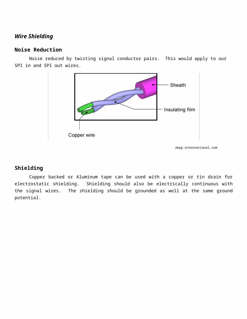
Wire Shielding
Noise ReductionNoise reduced by twisting signal conductor pairs. This would apply to our SPI in and SPI out wires.
Jmag-international.com
Shielding Copper backed or Aluminum tape can be used with a copper or tin drain for electrostatic shielding.
Shielding should also be electrically continuous with the signal wires. The shielding should be grounded as well at the same ground potential.

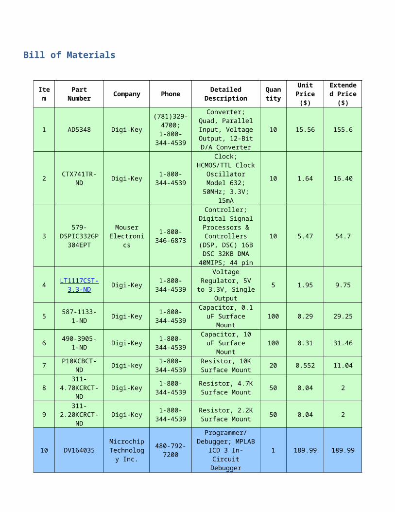
Bill of Materials
Item Part Number Company Phone Detailed Description
Quantity
Unit Price ($)
Extended Price ($)
1 AD5348 Digi-Key
(781)329-4700;
1-800-344-4539
Converter; Quad, Parallel Input,
Voltage Output, 12-Bit D/A Converter
10 15.56 155.6
2 CTX741TR-ND Digi-Key 1-800-344-
4539
Clock; HCMOS/TTL Clock Oscillator
Model 632; 50MHz; 3.3V; 15mA
10 1.64 16.40
3579-
DSPIC332GP304EPT
Mouser Electronics
1-800-346-6873
Controller; Digital Signal Processors &
Controllers (DSP, DSC) 16B DSC
32KB DMA 40MIPS; 44 pin
10 5.47 54.7
4 LT1117CST-3.3-ND Digi-Key 1-800-344-
4539
Voltage Regulator, 5V to 3.3V, Single
Output5 1.95 9.75
5 587-1133-1-ND Digi-Key 1-800-344-
4539Capacitor, 0.1 uF
Surface Mount 100 0.29 29.25
6 490-3905-1-ND Digi-Key 1-800-344-
4539Capacitor, 10 uF Surface Mount 100 0.31 31.46
7 P10KCBCT-ND Digi-key 1-800-344-
4539Resistor, 10K Surface Mount 20 0.552 11.04
8311-
4.70KCRCT-ND
Digi-Key 1-800-344-4539
Resistor, 4.7K Surface Mount 50 0.04 2
9311-
2.20KCRCT-ND
Digi-Key 1-800-344-4539
Resistor, 2.2K Surface Mount 50 0.04 2
10 DV164035Microchip
Technology Inc.
480-792-7200
Programmer/Debugger; MPLAB
ICD 3 In-Circuit Debugger
1 189.99 189.99
11 546-262F12 Mouser Electronics
1-800-346-6873
Transformer; PLATE AND FILAMENT;
26VA; 115V1 32.46 37.41
12 VOF-25-15 Digi-Key Co 1-800-344-4539
Converter, A/D, V-Infinity VOF-25 Series, PWR
SUPPLY 24W OPEN 15V 1.6A
1 20.76 25.98
13 bq20z75 Texas Instrument TBD Charging Circuit,
Evaluation Module 1 TBD TBD
14 Sonata 4400 Boston Power
1-508-366-0885
Battery, Lithium-Ion, provided by Dr.
Cheng4 0 0
15 TBD TBD TBD Litz Wire TBD TBD TBD
16 PL-700 RG-N Amphenol Alden
508-427-7045;
508-427-7014
Connector, 27 pin, Medical Disposable
Auto-Coupling Connectors
4 TBD TBD

17 9487T114 McMaster-Carr
404-629-6500
Wire, 36AWG, 0.1A, 0.012’’ (1.5 ft each) 14 0.52/1.5ft 7.28
18 7071K623 McMaster-Carr
404-629-6500
Wire, 22AWG, 2.8A, 0.052”; Flexible Wire 20 1.86/ft 37.2
19 69835K81 McMaster-Carr
404-629-6500
Wire, 26AWG, 4A, 0.039”, Harsh
Environment Wire (25ft)
1 2.08 2.08
20 9620T11 McMaster-Carr
404-629-6500
Wire, 30 AWG, 3A, High Flex, Silicone, L
= 2ft10 1.43/ft 28.60
21 7960K31 McMaster-Carr
404-629-6500
Heat Shrink Tubing, Di 0’’, thickness
0.015’’, L 6’’, Harsh Environment PTFE;
650F cure
40 3.45 138
22 73115K71 McMaster-Carr
404-629-6500
Heat Shrink Tubing, Di 0.0156’’, thickness
0.038’’, L 48”; Flexible; 275F
5 4.96 24.8
23 733K-ND Digi-Key 1-800-344-4539
Grommet, GROMMET
RUBBER .125" DIA10 0.114 1.14
24 92012A513 McMaster-Carr
404-629-6500
Screw, Hex, Alloy Steel, 4-40 Thread, 3/16’’ shldr L, 1/8’’
shldr dia.; 1/8’’ socket shldr screw (4
in pack)
4 3.08 12.32
25 90128A108 McMaster-Carr
404-629-6500
Screw, Hex, Zinc-Plated Alloy Steel, , 4-40 Thread, L=3/8’’
(25 in pack)
1 7.00 7.00
26 5229T47 McMaster-Carr
404-629-6500
Cord Stock, O-Ring, Round, 2-ft, Silicone,
Black2 0.78 1.56
27 2418T112 McMaster-Carr
404-629-6500
O-Ring, ID 1/8”; OD 1/4”; (150 in pack) 1 10.00 10.00
28 1832A14 McMaster-Carr
404-629-6500
Silicone, Loctite Nuva-Sil 5248,
10.1oz1 139.79 139.79
29 -- -- -- UV Light Lamp 1 -- --
30 P1 Brinkman Lab --
Casing, rapid-prototyping, ABS
plus4 -- --
31 113-1 Hellermann Tyton -- Heat Shrink Boot 21 TBD TBD
32 Polyurethane for TETTotal $975.35
Shipping (10%) $97.535
Total+ Shipping $1073

Test PlansIf any of the following tests fail, there is funding for components for two extra prototypes that will be
designed and re-designed according to test results.
LVAD Simulation Signal TestBefore testing the proposed prototype with the current LVAD set-up and with P10021 design, a test
simulating signals entering and leaving the designed transceivers will be conducted. Agilent 33120A Function/Arbitrary Waveform Generator will be used to simulate signals entering the device, and HP54602B Oscilloscope will be used to measure the output of the transceivers. The goal is to make sure that the signals are processed correctly, and each pin of the connector corresponds to appropriate pins of the connectors inside the body.
The following signals will be generated and measured:
LVAD position sensors (HESA) to XPC Control Target: Units Input Output
Signals from Summation Amplifiers to A/D Converter Count 2Voltage Volts 0 - 8Current mA 0 - 15Frequency Hz 0 - 600Sampling Rate ksps 5
Differential Amplifiers to A/D Converter Count 4
Voltage Volts -4 - 4Current mA 0 - 15Frequency Hz 0 - 600Sampling Rate ksps 5
XPC Control Target to Active Magnetic Bearings (AMB)
Signals from XPC Control Target to PWM Generator Count 4Voltage Volts 0 - 5 Current A -3 - 3 Frequency kHz 20
Speed Control signal from XPC Control Target to the LVAD Motor
Signal from XPC Control Target to Motor Controller Count 1Voltage Volts 0 - 5 Current mA 20Frequency MHz 40

Materials Needed:
1. HP 54602B Oscilloscope2. Agilent 33120A Function Waveform Generator
Start Date: __________ Finish Date:_______________
Engineer in charge: ________________________________
Comments:_____________________________________________________________
Wireless Power Transfer TestThe goal of this test is to demonstrate the wireless power transfer capability for the inductive power
transfer. The TET should transmit 30 Watts of power through human skin and tissue, however, a demonstration of the power transmission through the coils with air as the medium in between is sufficient for the demonstration. Voltage and current can be varied to represent
Materials Needed:
1. HP 54602B Oscilloscope2. Agilent 33120A Function Waveform Generator
Start Date: __________ Finish Date:_______________
Engineer in charge: ________________________________
Comments:_____________________________________________________________________
Trial #1:
Voltage In: __________ Voltage Out: _________
Current In: __________ Current Out: _________
Power In: ___________ Power Out: __________
Efficiency: ___________
Trial #2:
Voltage In: __________ Voltage Out: _________
Current In: __________ Current Out: _________
Power In: ___________ Power Out: __________
Efficiency: ___________
Trial #3:
Voltage In: __________ Voltage Out: _________

Current In: __________ Current Out: _________
Power In: ___________ Power Out: __________
Efficiency: ___________
Electronics Functionality Test
The
specifications above will be tested by plugging in the proposed device in two ways for a period of 6 hours to check the functionality of the device. One method is to test functionality of the new electronics with current system components; the second, is to test functionality with the design of the P10021 Senior Design Miniaturization team. To test functionality of the new electronics, we must have access to the current system components’ signals needed to test our design. Required signals are outlined in high-level design schematics and in specifications. Upon collaboration with P10021 Senior Design team, several criteria was agreed upon to allow for testing of both designs simultaneously for a period of 15 minutes. Observations will be made at 5 minute time intervals to ensure that the electronics are working properly, without any need for adjustments.
Equipment Needed:
1. Functional LVAD (provided by Dr. Cheng and Dr. Day)
2. Motor Controller, PWM Amplifiers, Summation and Differential Amplifiers connected to the LVAD (Provided by Dr. Cheng (current system) and P10021 Miniaturization Team).
3. XPC Controller and AC-DC Converter and Power Supply (if no functional TET)
Start Date: __________ Finish Date:_______________
Engineer in charge: ________________________________
Comments:____________________________________________________________________
Current System Test
Random Time Testing (mins) Functioning ( Yes / No) What is malfunctioning?
0
Eng. Spec. #
Importance Source Specification Description Unit of
MeasureIdeal Value
36 5 CN15 The device must demonstrate reliability, must function continuously for the testing period. Hours 6
37 5 CN16 Number of interruptions for the device's 6 hour cycle. Count 0
38 5 CN17 Number of user interventions for device's 6 hour cycle. Count 0
39 5 CN18 The device should work with the currently established system components. Boolean 1
40 3 CN19The device functions in accordance with Project #10021 (Miniaturization senior design team).
Boolean 1
30
60
P10021 Senior Design Team Project Test
Random Time Testing (mins) Functioning ( Yes / No) What is malfunctioning?
0
5
10
15
Flexibility TestThis test is designed to compare the flexibility of current cable used for control of the LVAD compared
to the proposed new design for the cable. Currently the cable consists of 23 wires bundled into a stainless steel cable covered with Loctite 5248 Alcoxy silicone. This cable will be tested for flexibility using the technique shown below. The cable will be securely clamped to a steady surface of a table leaving about 50 cm of cable free-hanging. A force will be applied with a spring scale pulling on the end of the cable. The scale will be used to read the amount of force applied, and the deflection will be measured with a measuring tape. The flexibility can be calculated from these values, and compared for both cables. Exactly the same conditions will be applied to both cables for easy and rough approximation. The goal is for the new design cable to have flexibility 200% (150% marginally) greater than the old cable, specified in Engineering Specifications #4. An average of three measurements will be taken.
Schematic
Equipment Needed
1. C-Clamp 2. Steady Table3. Measuring Tape4. Spring Scale (small scale)5. Current cable 4’’ sample6. New cable sample 4” sample
Start Date: __________ Finish Date:_______________
Engineer in charge: ________________________________

Are there any visual defects before or after testing? Yes / No … Yes / No
Comments:__________________________________________________________________
Average flexibility of old cable: _____________________
Average flexibility of new cable: ____________________
Alternative Method:The Taber Stiffness testing will be performed on samples of both the current cable and the new cable
by RIT Packaging Science Materials Laboratory. A percentage improvement of the new design over the old design will be calculated.
Equipment Needed:
1. Current cable 4’’ sample2. New cable sample 4” sample3. Taber 1575 Tester (RIT Packaging Science Laboratory)
Start Date: __________ Finish Date:_______________
Engineer in charge: ________________________________
Are there any visual defects before or after testing? Yes / No … Yes / No
Comments:__________________________________________________________________
Average flexibility of old cable: _____________________
Average flexibility of new cable: ____________________

Heat TestThis test is designed to ensure that the casing dissipates heat produced by electronics quickly, and the
electronics’ surface temperature does not increase by more than 6.4C over ambient. Also, the electronics must function properly and should not overheat if they are implanted into a body. This test covers customer needs #11 and #12, specified by engineering specifications #30 and #31. Simulating internal body fluids conditions is a tedious process, therefore, for feasibility purposes, the final product casing will be tested in water at 43C in a medium-sized oven for a period of 3 hours. A thermocouple will be used to measure temperature of electronics inside the casing, on the surface of the case, and the ambient temperature of surroundings. The electronics should be functioning fully the entire time, therefore, electronics will be supplied by the appropriate voltage and current using Agilent 33120A Function Waveform Generators.
Equipment Needed:
1. Medium Sized Oven – (~1 m3 volume) heated to 43C
2. Calibrated Thermocouples (3)
3. High Thermal Conductivity Tape
4. Agilent 33120A Function Waveform Generator (2 items)
5. HP 54602B Oscilloscope
6. Glass Bowl
7. Water at 43C
Start Date: __________ Finish Date:_______________
Engineer in charge: ________________________________
Are there any visual defects before or after testing? Yes / No … Yes / No
Comments:_____________________________________________________________________
Time (hrs)
Device Function (Yes /
No)
Inside the Casing (C)
Surface Temperature (C)
Oven Air Ambient
Temperature (C)
0
1
2
3

Drop TestTo fulfill engineering specifications #32 and #33, the drop test is designed to test for damage prevention
due to any accidental drops of the outside casing with electronics. The inner casing and electronics will also be tested by the same method to ensure that if the package can withstand this type of impact, it can withstand other kinds of unintentional impacts by outside forces, in cases of accidents, falls or other impacts. To simulate best a random fall, a person would drop the casing with electronics at random from a height of 1.5 meters onto a standard concrete surface, and any damage to the casing will be observed and recorded. Then, the electronics will be run in simulation, to ensure that they continue to function. If the casing or electronics are damaged, the casing shall be redesigned and re-fabricated.
Equipment Needed:
1. Measuring Tape2. HP 54602B Oscilloscope3. Agilent 33120A Function Waveform Generator
Start Date: __________ Finish Date:_______________
Engineer in charge: ________________________________
Are there any visual defects before or after testing? Yes / No … Yes/No
Comments:____________________________________________________________________
Trial #
Height of fall (m)
Damage to Casing
Scale (1 - no damage to 5 - dysfunctional)
Damage to Electronics
Scale (1 - no damage to 5 - dysfunctional)
Comments
1 1.5
2 1.5
3 1.5
4 1.5
5 1.5

Pressure and Leak TestThis test is designed to fulfill customer need #13, corresponding to engineering specification #34,
where the casing and the wire connections must withstand slightly higher pressures and be leak resistant under 1 meter of water. The casing and the cable carrying signal wires will be submerged in a tank under 1 meter of water, corresponding to pressure of 10 kPa. On one side of the casing the D Sub 15 connector will be connected, but the electronics will be removed; on the other side, the wires leaving the case should be intact. Ensure complete submersion, and keep steady under water for 15 minutes.
Equipment Needed:
1. Water2. ~1.5m deep container3. HP 54602B Oscilloscope4. Agilent 33120A Function Waveform Generator
Start Date: __________ Finish Date:_______________
Engineer in charge: ________________________________
Are there any visual defects or leaks before and after testing? Yes / No … Yes / No
Comments:_____________________________________________________________________

Risk Assessment


![INDEX [] · Web viewScale of Pay - 5200- 20200 Grade Pay (Rs.) - 1800,1900,2000,2400,2800 (iii) Category B – Pay Band - 2 Scale of Pay - 9300-34800 Grade Pay (Rs.) - 4200,4600,4800](https://static.fdocuments.net/doc/165x107/5b223e9e7f8b9a407b8b49f9/index-web-viewscale-of-pay-5200-20200-grade-pay-rs-18001900200024002800.jpg)


