EDC UNIT IV- Transistor and FET Characteristics
26
2008 EDC Lesson 9- " , Raj Kamal, 1 EDC UNIT IV- Transistor and FET Characteristics Lesson Lesson-9: 9: JFET and Construction of JFET and Construction of JFET JFET
Transcript of EDC UNIT IV- Transistor and FET Characteristics
2008 EDC Lesson 9- " , Raj Kamal, 1
EDC UNIT IV- Transistor and FET Characteristics
LessonLesson--9: 9: JFET and Construction of JFET and Construction of JFETJFET
2008 EDC Lesson 9- " , Raj Kamal, 2
1. Transistor1. Transistor
2008 EDC Lesson 9- " , Raj Kamal, 3
Transistor Definition Transistor Definition
The transferred-resistance or transistoris a multi-junction device that is capable of• Current gain• Voltage gain• Signal-power gain
2008 EDC Lesson 9- " , Raj Kamal, 4
2. Field Effect Transistor (FET)2. Field Effect Transistor (FET)
2008 EDC Lesson 9- " , Raj Kamal, 5
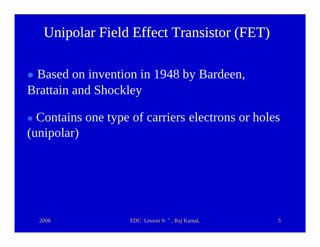
Unipolar Field Effect Transistor (FET) Unipolar Field Effect Transistor (FET)
Based on invention in 1948 by Bardeen, Brattain and Shockley
Contains one type of carriers electrons or holes (unipolar)
2008 EDC Lesson 9- " , Raj Kamal, 6
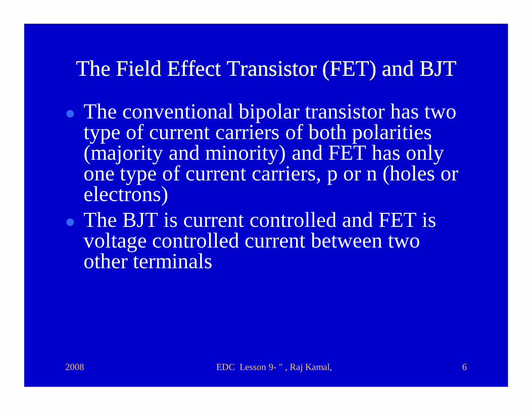
The conventional bipolar transistor has two type of current carriers of both polarities (majority and minority) and FET has only one type of current carriers, p or n (holes or electrons)
The BJT is current controlled and FET is voltage controlled current between two other terminals
The Field Effect Transistor (FET) and BJTThe Field Effect Transistor (FET) and BJT
2008 EDC Lesson 9- " , Raj Kamal, 7
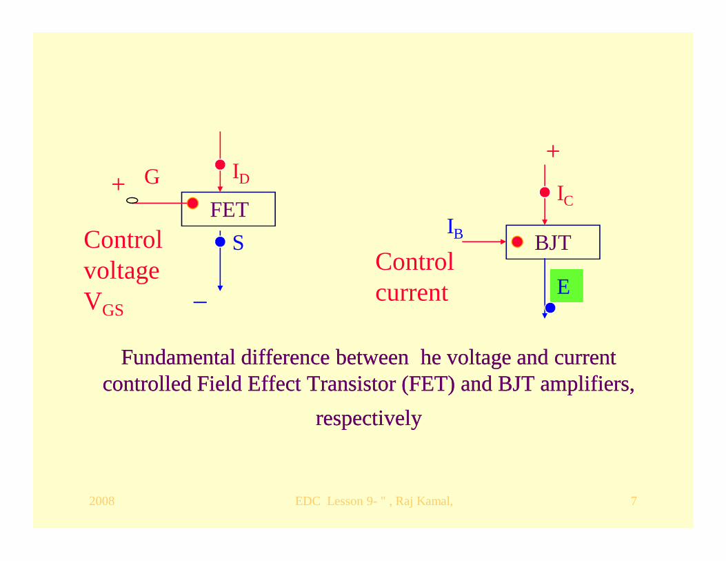
Fundamental difference betweenFundamental difference between tthe voltage and current he voltage and current controlled Field Effect Transistor (FET) and BJT amplifiers, controlled Field Effect Transistor (FET) and BJT amplifiers,
respectivelyrespectively
FET+ ID
S BJTControl current
IC
Control voltage VGS
G
– E
+
IB
2008 EDC Lesson 9- " , Raj Kamal, 8
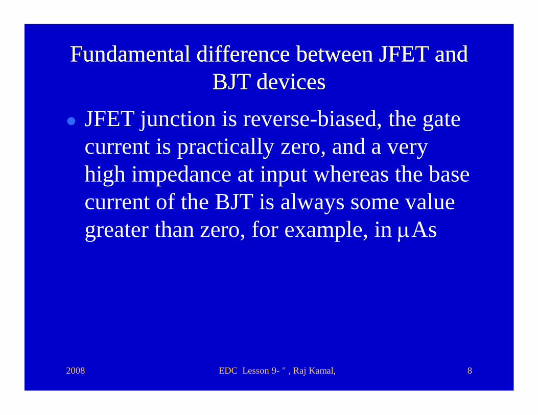
Fundamental difference between JFET and Fundamental difference between JFET and BJT devicesBJT devices
JFET junction is reverse-biased, the gatecurrent is practically zero, and a very high impedance at input whereas the base current of the BJT is always some value greater than zero, for example, in As
2008 EDC Lesson 9- " , Raj Kamal, 9
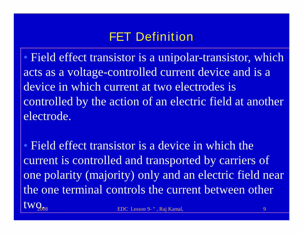
FET Definition
• Field effect transistor is a unipolar-transistor, which acts as a voltage-controlled current device and is a device in which current at two electrodes is controlled by the action of an electric field at another electrode.
• Field effect transistor is a device in which the current is controlled and transported by carriers of one polarity (majority) only and an electric field near the one terminal controls the current between other two.
2008 EDC Lesson 9- " , Raj Kamal, 10
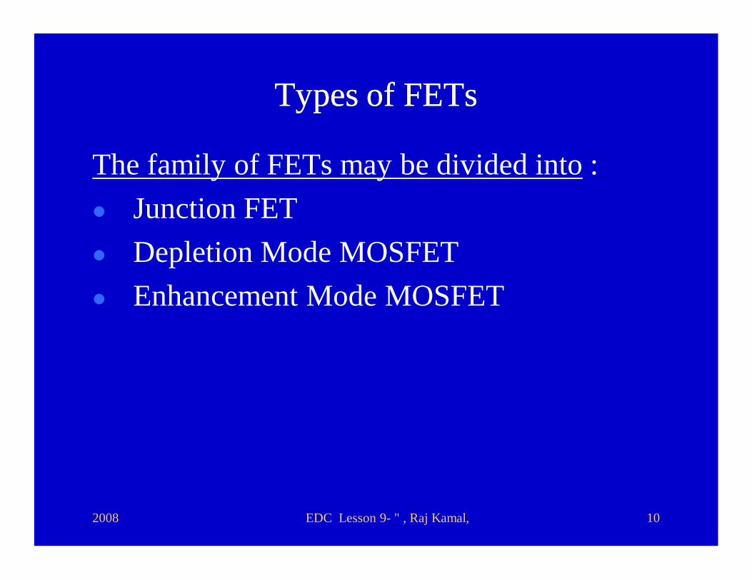
Types of FETsTypes of FETs
The family of FETs may be divided into : Junction FET Depletion Mode MOSFET Enhancement Mode MOSFET
2008 EDC Lesson 9- " , Raj Kamal, 11
3. Junction Field Effect Transistor (JFET)3. Junction Field Effect Transistor (JFET)
2008 EDC Lesson 9- " , Raj Kamal, 12
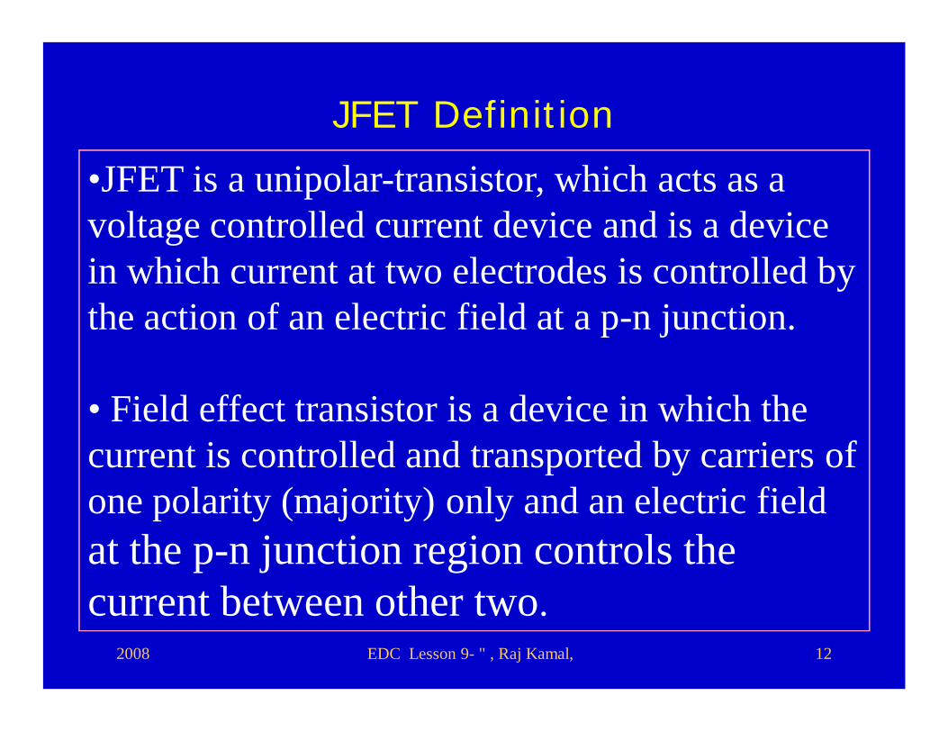
JFET Definition
•JFET is a unipolar-transistor, which acts as a voltage controlled current device and is a device in which current at two electrodes is controlled by the action of an electric field at a p-n junction.
• Field effect transistor is a device in which the current is controlled and transported by carriers of one polarity (majority) only and an electric field at the p-n junction region controls the current between other two.
2008 EDC Lesson 9- " , Raj Kamal, 13
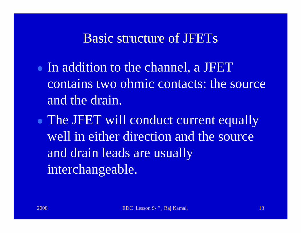
Basic structure of JFETsBasic structure of JFETs
In addition to the channel, a JFET contains two ohmic contacts: the source and the drain.
The JFET will conduct current equally well in either direction and the source and drain leads are usually interchangeable.
2008 EDC Lesson 9- " , Raj Kamal, 14
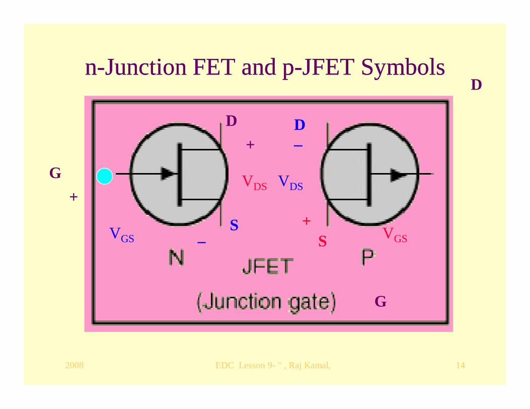
nn--Junction FET and pJunction FET and p--JFET SymbolsJFET Symbols
G+
D+
S–VGS
VDS
G
D
D
+VGS
VDS
S
2008 EDC Lesson 9- " , Raj Kamal, 15
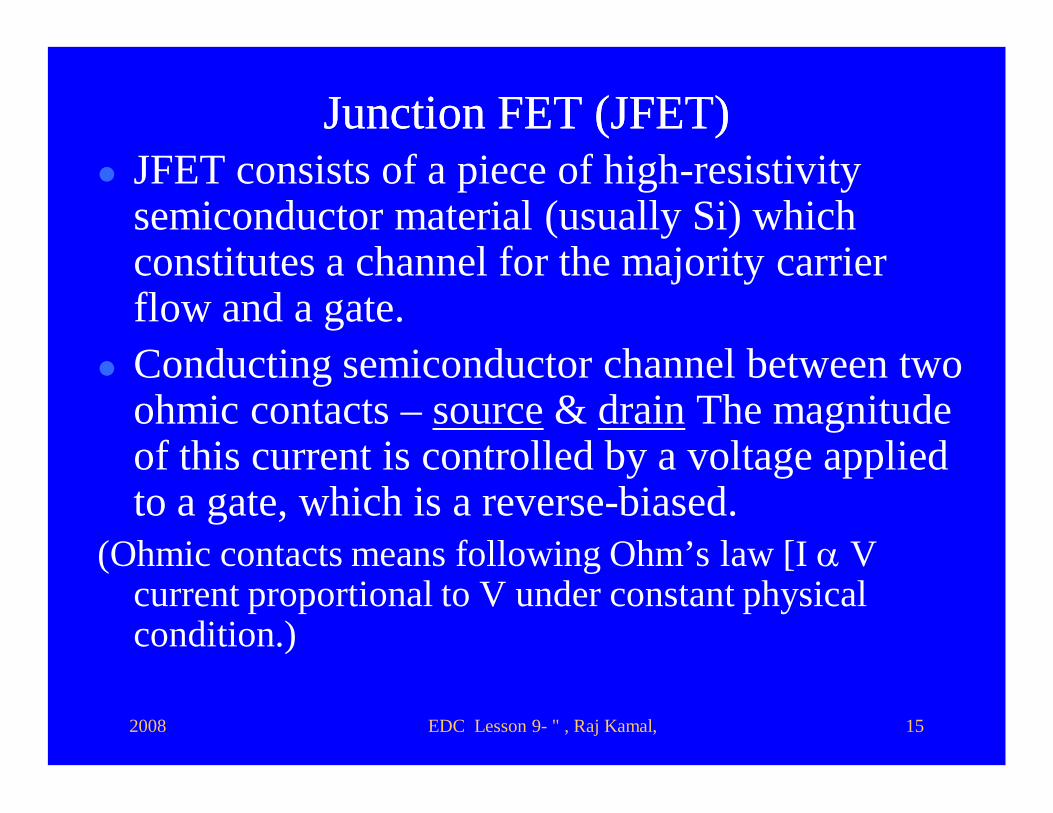
Junction FET (JFET)Junction FET (JFET) JFET consists of a piece of high-resistivity
semiconductor material (usually Si) which constitutes a channel for the majority carrier flow and a gate.
Conducting semiconductor channel between two ohmic contacts – source & drain The magnitude of this current is controlled by a voltage applied to a gate, which is a reverse-biased.
(Ohmic contacts means following Ohm’s law [I V current proportional to V under constant physical condition.)
2008 EDC Lesson 9- " , Raj Kamal, 16
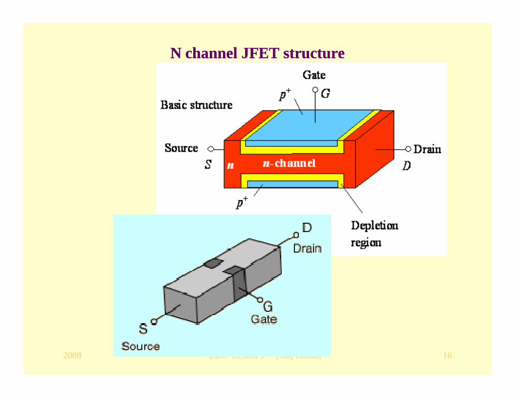
N channel JFET structureN channel JFET structure
2008 EDC Lesson 9- " , Raj Kamal, 17
NN--channel JFET construction channel JFET construction
This transistor is made by forming a channel of N-type material in a P-type substrate.
Three wires are then connected to the device. One at each end of the channel. One connected to the substrate. In a sense, the device is a bit like a PN-
junction diode, except that there are two wires connected to the N-type side.
2008 EDC Lesson 9- " , Raj Kamal, 18
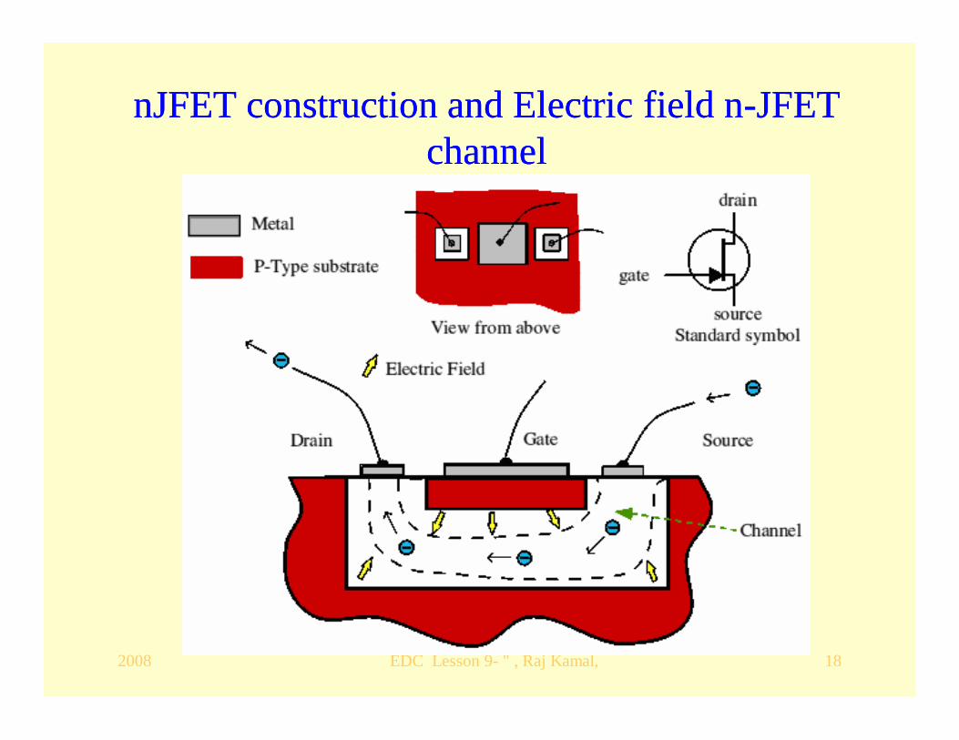
nJFET construction and Electric field nnJFET construction and Electric field n--JFET JFET channelchannel
2008 EDC Lesson 9- " , Raj Kamal, 19
nn--Junction FETs and pJunction FETs and p--JFETsJFETs JFET is a high-input resistance device, while the
BJT is comparatively low. If the channel is doped with a donor impurity, n-
type material is formed and the channel current will consist of electrons.
If the channel is doped with an acceptor impurity, p-type material will be formed and the channel current will consist of holes.
2008 EDC Lesson 9- " , Raj Kamal, 20
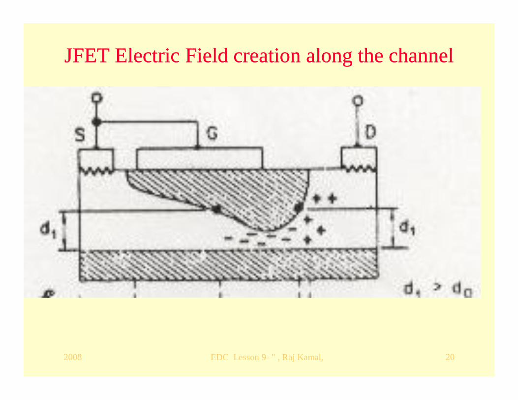
JFET Electric Field creation along the channelJFET Electric Field creation along the channel
2008 EDC Lesson 9- " , Raj Kamal, 21
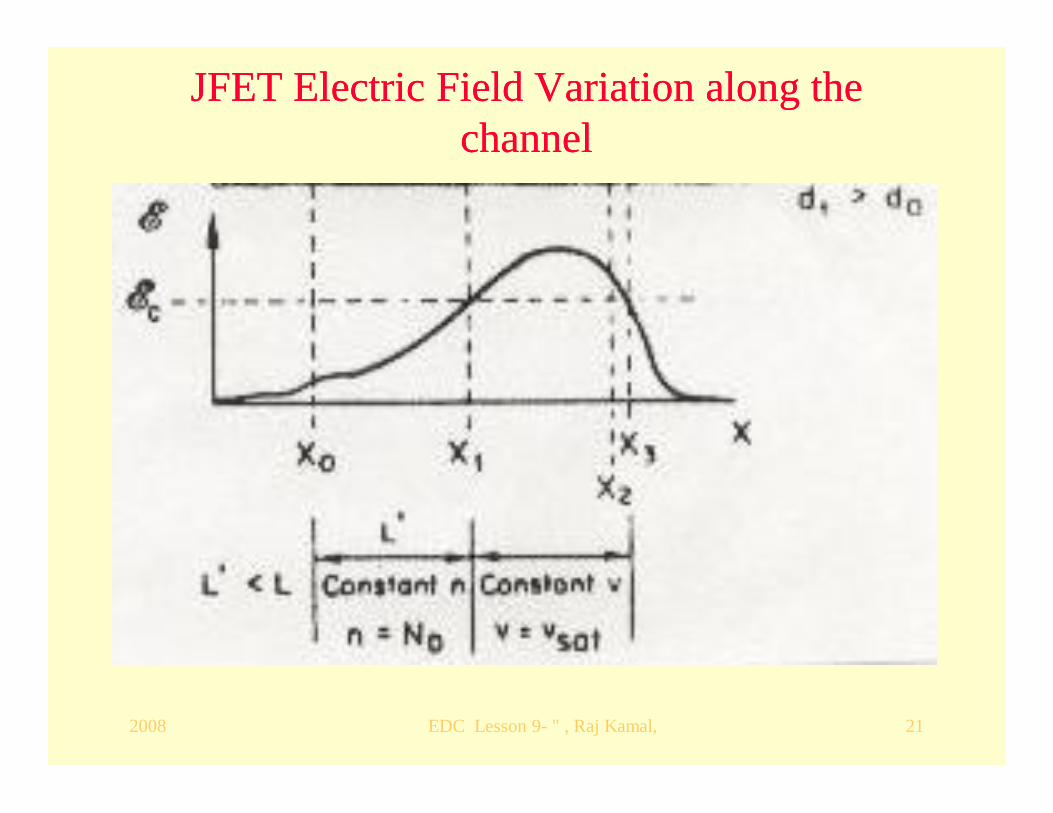
JFET Electric Field Variation along the JFET Electric Field Variation along the channelchannel
2008 EDC Lesson 9- " , Raj Kamal, 22
nn-- JFET and pJFET and p--JFET JFET
N-channel JFET have greater conductivity than p-channel types, since electrons have higher mobility than do holes; thus n-channel JFETs are approximately twice as efficient conductors compared to their p-channel counterparts.
2008 EDC Lesson 9- " , Raj Kamal, 23
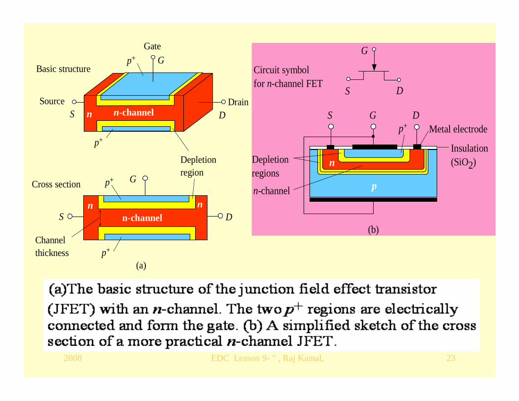
DS n-channeln
Gate
DrainSource
GBasic structure
p+
p+
n
Depletionregion
S Dn-channel
GCross section
n
Channelthickness
p+
p+
(a)
nDepletionregions
n-channel
Metal electrode
Insulation(SiO2)
p
S DGp+
(b)
DS
G
Circuit symbolfor n-channel FET
2008 EDC Lesson 9- " , Raj Kamal, 24
SummarySummary
2008 EDC Lesson 9- " , Raj Kamal, 25
We learnt• Definitions of transistor, FET and
JFET• Construction JFET• n-channel and p-channel JFET
2008 EDC Lesson 9- " , Raj Kamal, 26
End of Lesson 9End of Lesson 9