ECE317 : Feedback and Controlweb.cecs.pdx.edu/~tymerski/ece317/ECE317 L14_BodeDesign...ECE317 :...
36
ECE317 : Feedback and Control Lecture : Design using Bode plots, compensation Dr. Richard Tymerski Dept. of Electrical and Computer Engineering Portland State University 1
Transcript of ECE317 : Feedback and Controlweb.cecs.pdx.edu/~tymerski/ece317/ECE317 L14_BodeDesign...ECE317 :...
ECE317 : Feedback and Control
Lecture :Design using Bode plots, compensation
Dr. Richard Tymerski
Dept. of Electrical and Computer Engineering
Portland State University
1

Course roadmap
2
Laplace transform
Transfer function
Block Diagram
Linearization
Models for systems
• electrical
• mechanical
• example system
Modeling Analysis Design
Stability
• Pole locations
• Routh-Hurwitz
Time response
• Transient
• Steady state (error)
Frequency response
• Bode plot
Design specs
Frequency domain
Bode plot
Compensation
Design examples
Matlab & PECS simulations & laboratories
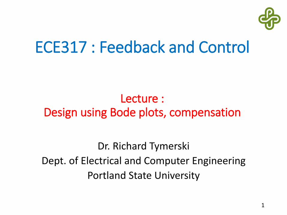
Notes on Bode plot (review)
• Advantages• Without computer, Bode plot can be sketched easily by
using straight-line approximations.
• GM, PM, crossover frequencies are easily determined on Bode plot.
• Controller design on Bode plot is simple.
3

4
Compensators

5
Application to the lab:

6
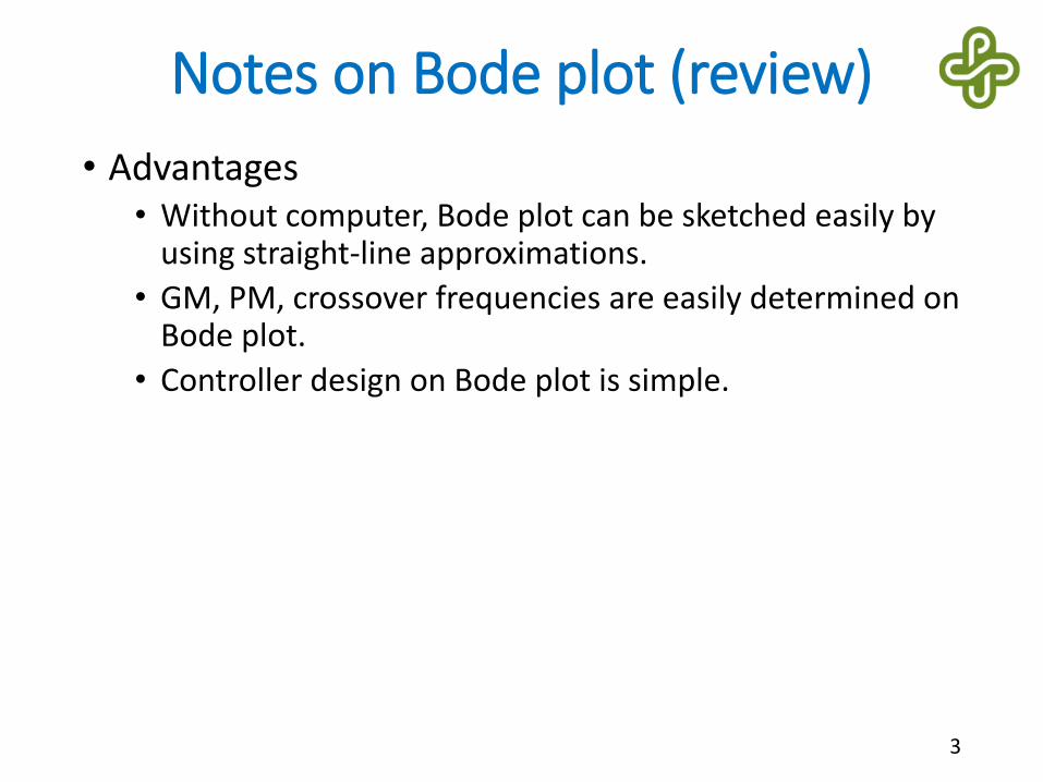
Uncompensated SystemLoop Gain, T(s):
7
Uncompensated SystemLoop Gain, T(s):
Example used here:

8
Uncompensated SystemAsymptotic Bode plot:
Phase margin = 0∘
⇒ compensator is needed
9
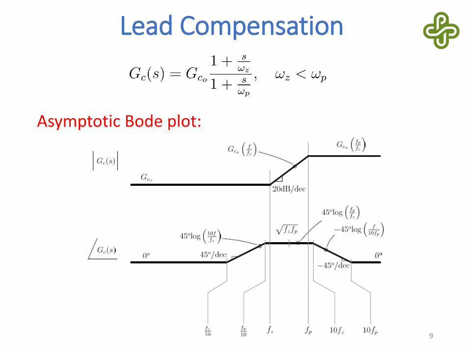
Lead Compensation
Asymptotic Bode plot:
10
Lead Compensation
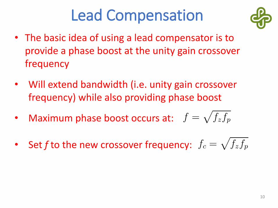
• Maximum phase boost occurs at:
• Set f to the new crossover frequency:
• Will extend bandwidth (i.e. unity gain crossover frequency) while also providing phase boost
• The basic idea of using a lead compensator is to provide a phase boost at the unity gain crossover frequency
11
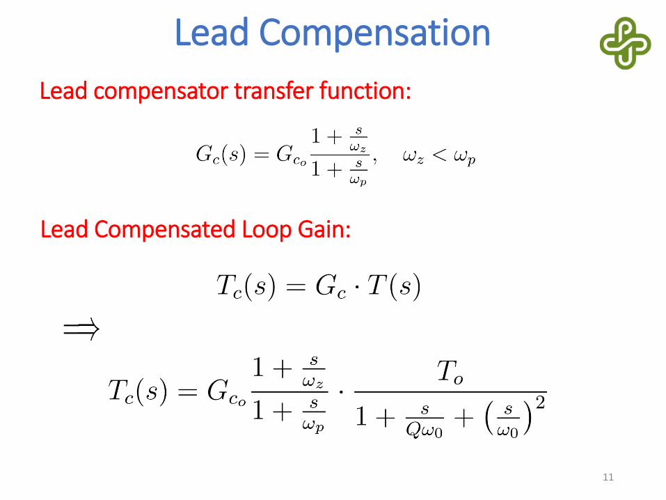
Lead Compensation
Lead Compensated Loop Gain:
Lead compensator transfer function:
12
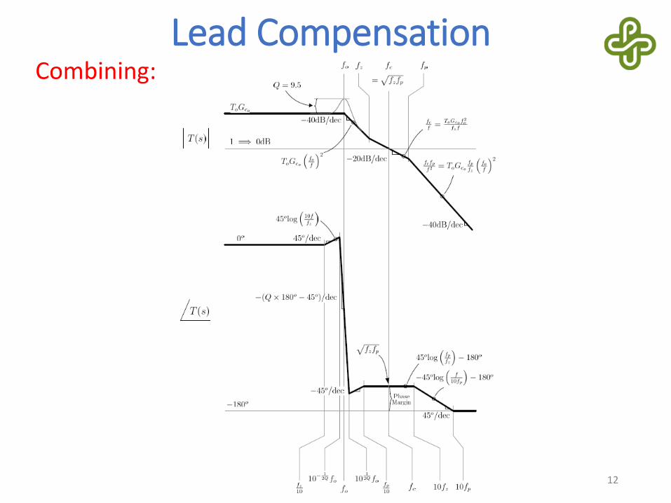
Lead CompensationCombining:

13
Lead CompensationFocusing around 𝑓𝑐:
Phase margin:
14
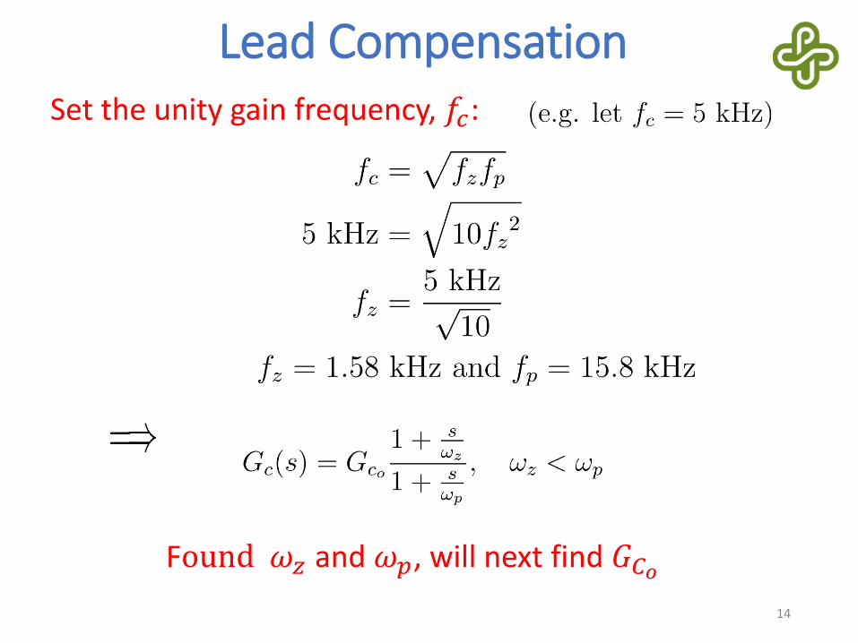
Lead CompensationSet the unity gain frequency, 𝑓𝑐:
Found 𝜔𝑧 and 𝜔𝑝, will next find 𝐺𝐶𝑜
15
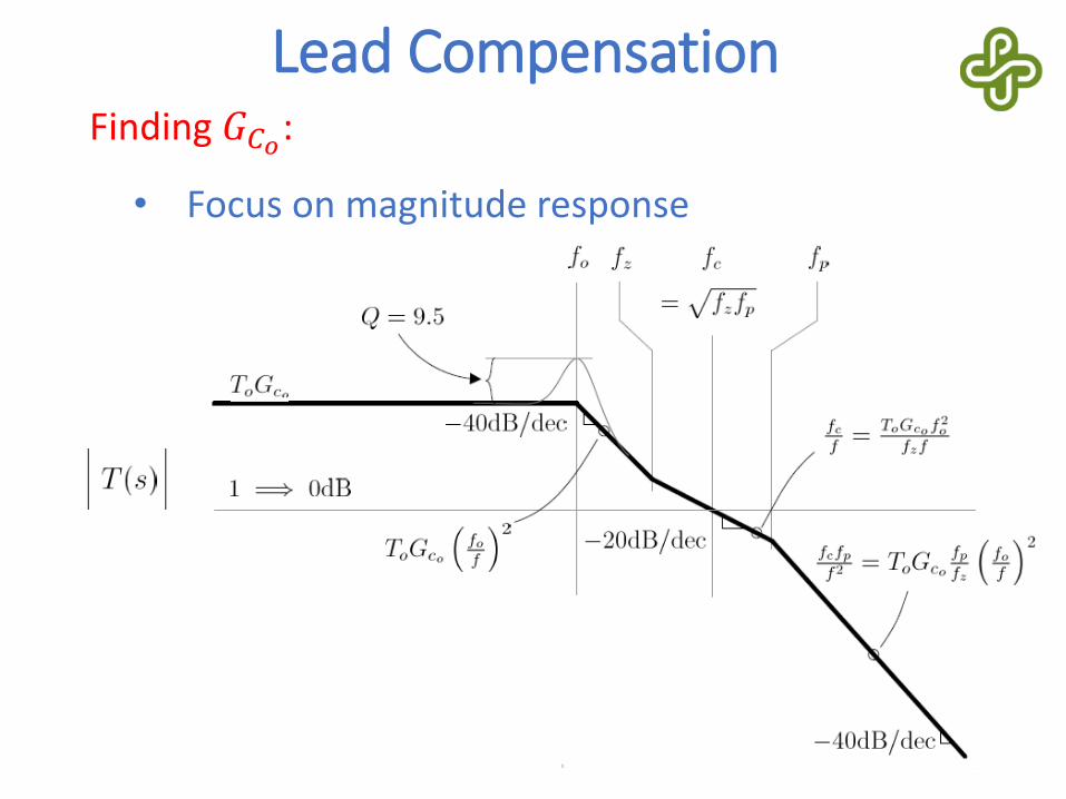
Lead CompensationFinding 𝐺𝐶𝑜
:
• Focus on magnitude response
16
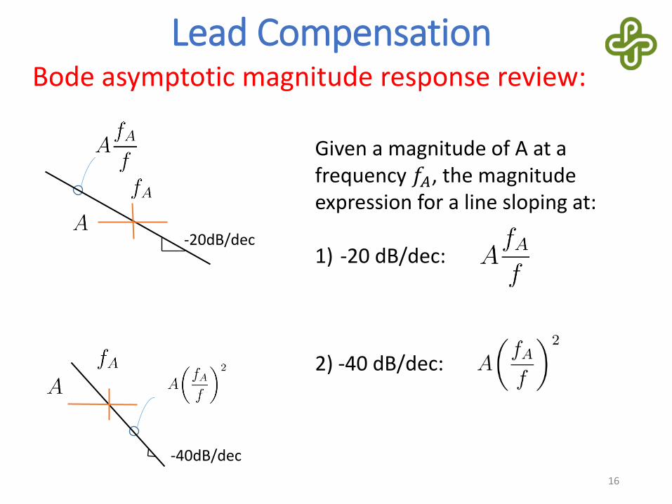
Lead CompensationBode asymptotic magnitude response review:
-20dB/dec
-40dB/dec
Given a magnitude of A at a frequency 𝑓𝐴, the magnitude expression for a line sloping at:
1) -20 dB/dec:
2) -40 dB/dec:
17
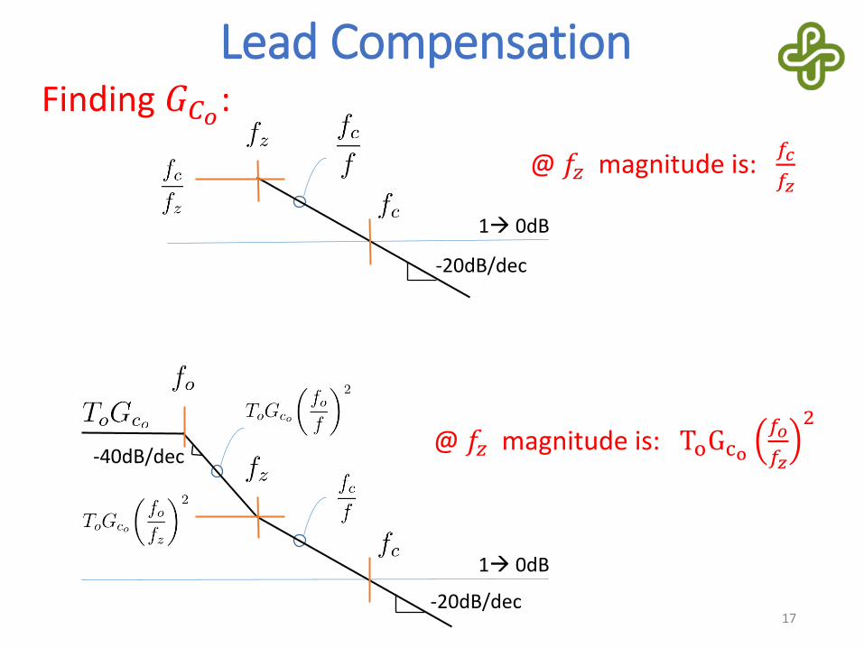
Lead CompensationFinding 𝐺𝐶𝑜
:
-20dB/dec
1 0dB
-20dB/dec
1 0dB
-40dB/dec
@ 𝑓𝑧 magnitude is: 𝑓𝑐
𝑓𝑧
@ 𝑓𝑧 magnitude is: ToGco
𝑓𝑜
𝑓𝑧
2
18
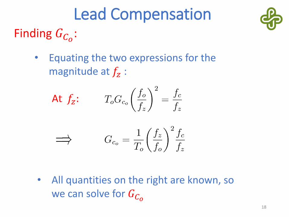
Lead CompensationFinding 𝐺𝐶𝑜
:
At 𝑓𝑧:
• Equating the two expressions for the magnitude at 𝑓𝑧 :
• All quantities on the right are known, so we can solve for 𝐺𝐶𝑜

19
Lead Compensation
𝐺𝑐𝑜= 3.4
Finding 𝐺𝐶𝑜:
Design of lead compensator is complete

20
Lead CompensationExact loop gain using Matlab :
Phase margin = 55.9∘

21
Lead CompensationTime response to input voltage change using PECS:
Non-zero steady state error
Need a different compensator to null SS error

22
Dominant Pole with Lead Compensation
Given the following magnitude response, what is the transfer function?:
-20dB/dec
Answer:1) The low frequency asymptote is that of a pole at zero where
the magnitude at 𝑓𝐴 is A A𝜔𝐴
𝑠
2) This is followed by a zero at 𝑓𝐴: 1 +𝑠
𝜔𝐴
3) Combining results in transfer function: A𝜔𝐴
𝑠1 +
𝑠
𝜔𝐴
New Compensator:

23
-20dB/dec
1 0dB
-40dB/dec
Dominant Pole with Lead Compensation
-20dB/dec
-20dB/dec
1 0dB
-40dB/dec
-20dB/dec
+
Combining: 1) Set 𝑓𝐴 (where 𝑓𝐴 ≤ 𝑓𝑜)2) Adjust A to match low frequency
magnitude 𝑇𝑜𝐺𝑐𝑜 lead
Lead compensated system:
Added low frequency compensation:

24
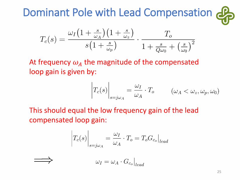
Dominant Pole with Lead Compensation
Compensated loop gain:
25
Dominant Pole with Lead Compensation
At frequency 𝜔𝐴 the magnitude of the compensated loop gain is given by:
This should equal the low frequency gain of the lead compensated loop gain:
26
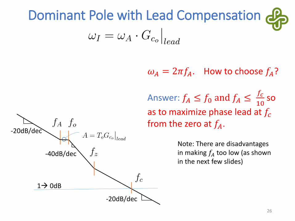
Dominant Pole with Lead Compensation
𝜔𝐴 = 2𝜋𝑓𝐴. How to choose 𝑓𝐴?
Answer: 𝑓𝐴 ≤ 𝑓0 and 𝑓𝐴 ≤𝑓𝑐
10so
as to maximize phase lead at 𝑓𝑐from the zero at 𝑓𝐴.
-20dB/dec
1 0dB
-40dB/dec
-20dB/dec
Note: There are disadvantages in making 𝑓𝐴 too low (as shown in the next few slides)

27
Dominant Pole with Lead Compensation
Design of Dominant Pole with Lead Compensator is now complete
Compensator transfer function:
Four parameters needed to be determined:𝜔𝑧, 𝜔𝑝, 𝜔𝐴, and 𝜔𝐼
• Let’s look closer at the how to choose 𝜔𝐴
(which also changes the value of 𝜔𝐼)
28
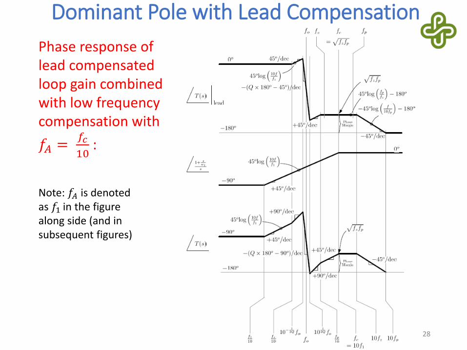
Dominant Pole with Lead Compensation
Phase response of lead compensated loop gain combined with low frequency compensation with
𝑓𝐴 =𝑓𝑐
10:
Note: 𝑓𝐴 is denoted as 𝑓1 in the figure along side (and in subsequent figures)

29
Dominant Pole with Lead Compensation
Asymptotic Bode plot for compensated loop gain
(𝑓𝐴 =𝑓𝑐
10) :
Note: 𝑓𝐴 is denoted as 𝑓1 in the figure along side

30
Dominant Pole with Lead Compensation
Exact Bode plot for compensated loop gain (𝑓𝐴 =𝑓𝑐
10) :
Phase margin = 50.5∘

31
Dominant Pole with Lead Compensation
Associated time response to input voltage change:
Settling time ≈ 1 ms

32
Dominant Pole with Lead CompensationPhase response of lead compensated loop gain combined with low frequency compensation with
𝑓𝐴 =𝑓𝑐
33:
Note: 𝑓𝐴 is denoted as 𝑓1 in the figure along side

33
Dominant Pole with Lead CompensationAsymptotic Bode plot for compensated loop gain
(𝑓𝐴 =𝑓𝑐
33) :
Note: 𝑓𝐴 is denoted as 𝑓1 in the figure along side

34
Dominant Pole with Lead Compensation
Exact Bode plot for compensated loop gain (𝑓𝐴 =𝑓𝑐
33) :
Phase margin = 54.3∘

35
Dominant Pole with Lead CompensationAssociated time response to input voltage change:
Slower settling time
The first design is better
Settling time ≈ 4 ms
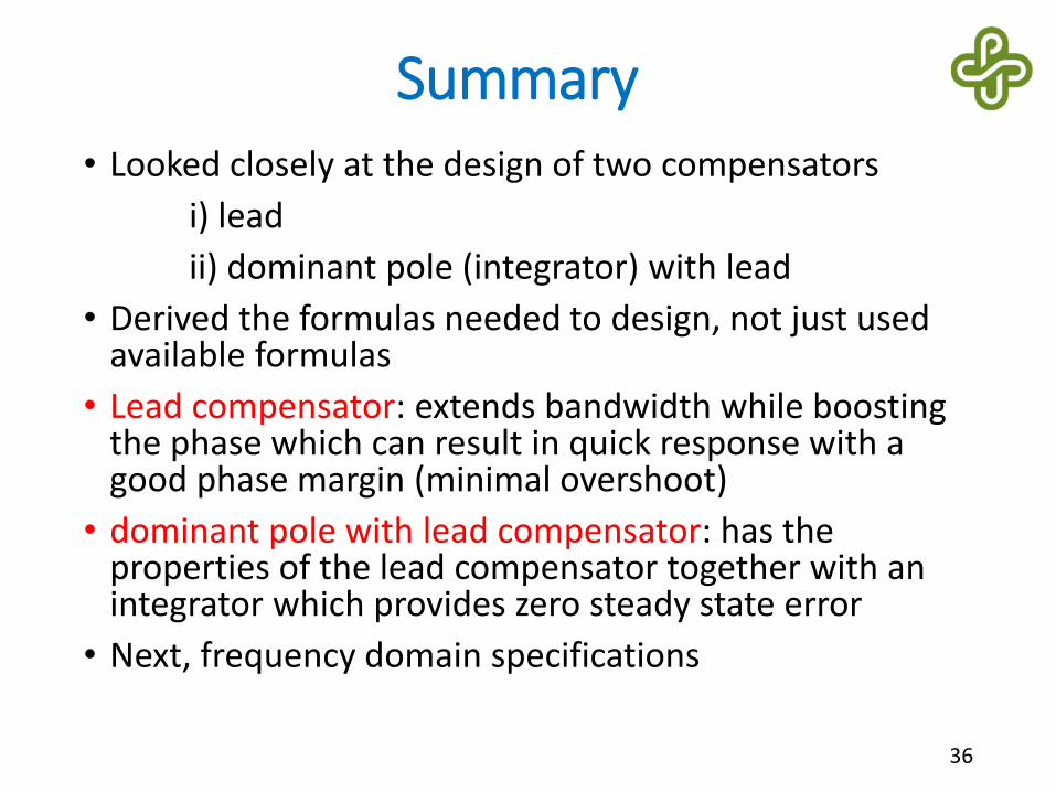
Summary• Looked closely at the design of two compensators
i) lead
ii) dominant pole (integrator) with lead
• Derived the formulas needed to design, not just used available formulas
• Lead compensator: extends bandwidth while boosting the phase which can result in quick response with a good phase margin (minimal overshoot)
• dominant pole with lead compensator: has the properties of the lead compensator together with an integrator which provides zero steady state error
• Next, frequency domain specifications
36