Photosensitive diodes and transistors Light emitting diodes Photocouplers Infrared sensitive
Upload
piers-mccormickCategory
view
228download
0
ECE 662Microwave Devices
Microwave Materials,
Diodes and TransistorsFebruary 3, 2005


Two-Terminal Negative Resistance Devices
Varactor – small pn diodes that are operated as nonlinear capacitorsIn the reverse bias region

Application of Negative Resistance Devices
0R impedance sticcharacteri
real positive a hasport -2 The
DeviceMultiport ReciprocalNon
eddemonstrat 100GHz
ashigh as up 2%),( efficiency low mW, outputs,power LowgeDisadvanta
voltage)bandgap(larger GaAs(usually fabricate easy to Simple, Advantage
gain. infinitewith amplifier or oscillatoran like acts so then ,RR If
,RR-
RR- ,RR when
RR
RR
ZZ
ZZΓ t,coefficien Reflection
0
0
0L
0L
0L
0L
0L

Varactor• Varactor = Variable reactor• Use of voltage-variable properties (such as
capacitance) of reversed-biased p-n junctions
• Reverse biased depletion capacitance is given by Cj ~ (Vb + VR)-n or Cj ~ (VR)-n for VR >> Vb, where n = ⅓ for a linearly graded junction and n = ½ for an abrupt junction.
• Can further increase the voltage sensitivity by using a hyperabrupt junction having an exponent n greater than ½.

Charge Depletion Regions
22
d2
21
a1
2211
d
1a
12
212a
1aa
2
2
a
2
2
2
2
2
eN and
2
eN
VVXat x and -VV-Xat x also
eN with material type-nfor repeat
eN0
dx
dV & 0C 0)0V(x :conditionsboundary
2
eNeNeN- -eN
0)(xregion material type-pIn
1
XVXV
XC
CxCxVCxdx
dV
dx
Vd
dx
Vd
dx
V
Xx

Charge Depletion Regions
bias. reversefor negative is V whereV,VV
,V)NN(2
NN
dV
dQ C area,unit per
ecapacitanc separation chargeSi,for temproom @
1045.1n ;n
NNlnV also
)N/N1(eN
2 &
)N/N1(eN
2
equality) charge(NNbut
)N(N2
eV PotentialContact
BT
1/2
2/1
da
da
310i2
i
daB
1/2
add2
1/2
daa1
2d1a
22d
21a21B
T
e
cme
kT
VX
VX
XX
XXVV
BB

Varactor• Present applications mostly for harmonic
generation at millimeter and sub millimeter wave frequencies and tuning elements in various microwave applications.
• A common varactor is the reversed biased Schottky diode.
• Advantages: low loss and low noise.• Produces only odd harmonics when a
sinusoidal signal is applied, so a frequency tripler can be realized without any second harmonic.

Varactor
THz. 1 isvaractor
art theof state afor f of valueTypical
resistance series
theis R where,2
/1/1f
:merit) of figureimportant an (
Frequency Cutoff Dynamic
c
smaxmin
csR
CC

Varactor Frequency Multipliers
• Provide LO power to sensitive millimeter and sub-millimeter wavelengths receivers.
• Schottky doublers can deliver 55 mW at 174 GHz
• Heterostructure Barrier Varactor Diodes acting as triplers deliver about 9mW at 248 GHz.

Crossed Waveguide Frequency Multiplier Ref. Golio

Varactor Devices
• Lower frequencies: reversed biased semiconductor abrupt p+-n juction diodes made from GaAs or Si.
• Higher frequencies: Schottky diodes (metal-semiconductor junction diodes
• High frequencies and power handling: heterostructure barrier varactor – several barriers stacked epitaxially
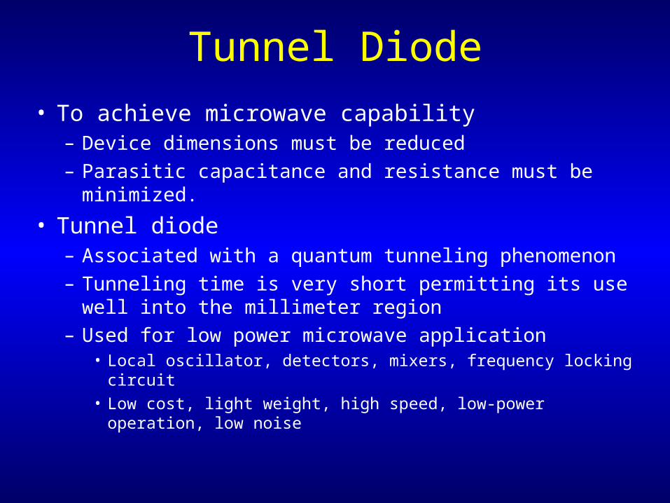
Tunnel Diode
• To achieve microwave capability– Device dimensions must be reduced
– Parasitic capacitance and resistance must be minimized.
• Tunnel diode– Associated with a quantum tunneling phenomenon
– Tunneling time is very short permitting its use well into the millimeter region
– Used for low power microwave application• Local oscillator, detectors, mixers, frequency locking circuit
• Low cost, light weight, high speed, low-power operation, low noise

Tunnel Diode• In classical case, particle is reflected if E<
potential barrier height of V0
• In quantum case particle has a finite probability to transmit or “tunnel” the potential barrier
• Single p-n junction which has both p & n sides heavily dopeddepletion regions very narrow and tunneling distance is small ~ 50 to 100 Å– (1 Å =10-8 cm=10-4 m)– High dopings cause Fermi levels within allowable
bands

p-n junction

Tunnel Diode- abrupt junctions of heavily doped p & n
semiconductor material p~n~1019

Tunnel Diode• 1) For zero bias - electrons tunneled
through narrow barrier at equal rates in each direction. Net current zero.
• 2) Small forward bias - electrons at bottom of conductor band on n side are are raised to energy levels corresponding to unoccupied energy levels on the p side. Therefore, tunneling current in forward direction with increases with bias.

Tunnel Diode• 3) For still larger bias, more and more
electrons are raised to levels lying opposite the forbidden band on p side to which to which no tunneling is possible therefore the current reduces with increasing bias.
• 4) As bias increases further, the current remains small until minority carrier injection similar to conventional diodes predominates.

Tunnel Diode• 5) with reverse as an increasing number of
electrons on the p side find themselves opposited allowed and empty levels in the conduction band on the n side therefore tunneling increases rapidly with increasing bias.

Application of Negative Resistance Devices
diode.
for tunnelmerit of figure/II
.resistance negative theof magnitude
thedetermine I and I of Values
vp
vp
mW) (fewpower output low very -
GHz) 100 to(upfrequency high noise, low
operation,power low speed,high ht,light weig cost, low
1exp1
1expII
bygiven is sticcharacteri V-Ifor form Empirical
11
0p
pp
p
p
pp
V
V
V
I
V
V
dV
dIR
IV
V
V
V
Note negative resistance

Tunnel Diode
Note that small changes in VB result in large changes in i hence VRL
Negative Resistance Devices I & V, 180 out of phase I2R power absorbed, but if R –R then power generated


Summary of Tunnel Diode
• Quantum Tunneling Phenomena
• Tunneling time short - mm waves
• Low-power applications
• n-p sides so heavily doped that the fermi levels lie within the conduction and valence bands
• Good for extreme speed
• Rate of tunneling can change as fast as energy levels can be shifted
• Devices such as transistors give more power, but traditionally have suffered in speed due to rate of diffusion of charge changing.

Solid-State Device Power
Output vs Frequency
ref: Sze and
modifiedby Tian

Transistors• Bipolar (Homojunction)
– Inexpensive, durable, integrative, relatively high gain
• Bipolar (Heterojunction)– High speed switching
• Field Effect Transistors– Junction– MESFET, MOSFET, High Electron Mobility
(HEMT)– Av as well as Qc, better efficiency, lower noise
figure, higher speed, high input impedance


pnp transistor with all leads grounded
ref. Sze

pnp transistor in the active mode of operation
ref. Sze

Various current components in a p-n-p transistor under the active mode of operation. ref. Sze
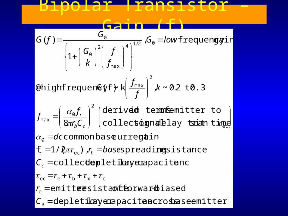
Bipolar Transistor – Gain (f)
emitter-base across ecapacitanclayer depletion
biased-forward of resistanceemitter
ecapacitanclayer depletion collector
resistance spreading ),2/(1f
gaincurrent basecommon
sit time,delay tran signalcollector
emitter to of in terms derived
8
0.3 to2.0~,k~G(f)frequency @high
gainfrequency ,
1
)(
e
cxbeec
ec
0
ec
2
0max
2
max
02/14
max
2
0
0
e
c
b
cb
C
r
C
baser
dc
Cr
ff
kf
f
lowG
ff
kG
GfG

Bipolar Transistor – Gain (f) – cont.
ecapacitanclayer depletion base-collector
collector
theofregion undepleted with theassociated resistance
timecharginglayer depletion
cm/sec 10 8 ~ electrons of velocity v
regiondepletion collector -base ofwidth W
region.depletion
collector-base he through tcarriers of time)2/(
base in the electrons injectedemitter ofconstant
width Wbase he through t
carriers of ime transit tlimited-Diffusion)5.3/(
c
6s
c
x
b
2
c
c
cc
sc
eb
ebb
C
r
collectorCr
saturation
transitvW
diffusionD
DWb

Bipolar Transistor – High Freq.
areae/unit capacitanccollector )(
)(width w base ofpart undepleted ofy resistivit average
)/()(
00
b
CCsWC
wsWr
c
b
bbb

Bipolar Transistor – Gain (f)
MHz 400f m,25Lfor
or GHz 3f m,3Lfor :;2
f
m,15.0 wm;1 widthsstrip typically,w
1f
nD
w,
w
)(4
1f
b2/1b
max
eb
2b
2/1
0
b0max
L
v
CsW becbec

Field-Effect Transistors
• Advantages – 1) Voltage gain and current gain
(simultaneously)– 2) Higher efficiency compared to bipolar– 3) Lower Noise Figure
– 4) Higher fmax and consequently higher operating frequency
– 5) High input resistance, up to several Meg

Field-Effect TransistorsV is changed by Vgs – to change channel size {reverse bias between Source and gate to adjust channel forward bias between source andDrain for current flow (majority carrier)}
(Si) kV/cm 15E @ 108~v
GaAs) (3kV/cm,E@ 102~citydrift velo saturation vlength, gateL
ime, transit tL/v ,22
1~f ;
f
fk ~G bipolar,
Like channel, of dopingN and m0.15 ~ channel of width a wherevoltage,
off-pinch 2
0yat 0V b.c. )2(2
ayat 0 b.c. )(
6s
7s
smax
2
max
22
2
2
gatewhereL
v
qNaVayVayy
qNV
dy
dVay
qN
dy
dVqN
dy
Vd
s
p

Field-Effect Transistors
GHz 60~f GaAsfor velocity saturationlarger isKey
microns)in length Gate(
32f GaAsFor
max
max
L
GaAs FET Bipolar Xtr.
Gain 20 – 40 dB ~10 dB
BW Several GHz Several 1/10 GHz
Power Out 0.5 to 5 W 20 W
fmax ~ 8 GHz ~ 3 GHz
Pfmax2 ~ 3x10²⁰ WHz2 ~ 2x10²⁰ WHz2

Field-Effect Transistors
• To get larger output powers – use larger gate widths– ~ 1W / 1 mm gate width
• Single gate width ~ 250 to 500 m
• Use multiple gates (~12) to increase power

Technology Alternatives - 1 Ref: MPD, Nov 2002, Amcom Communications
• Material technologies (GaAs, Si, SiGe)
• Process technologies (Epitaxy, Implant)
• Device technologies (BJT, HBT, MESFET, HEMT)
• Power levels less than 1 W– BJT, HBT (use single polarity supply and offer
cost advantages at these power levels)– GaAs, MESFET’s, pHEMT’s (better linearity
and efficiency)

Technology Alternatives - 2 Ref: MPD, Nov 2002, Amcom Communications
• High power levels above 10 W– Si LDMOS (attractive at frequencies below 2
GHz)– Wide band gap devices such as SiC,
MESFET’s, GaN, HEMT’s (higher power, higher voltage and promising linearity performance)

Terrestrial wireless systems Ref: MPD,
Nov 2002, Amcom Communications
Broadband internet access – operate in the frequency range of 1 – 6 GHz.
Low cost subscriber units: less than 1 W transmit power: SiGe, GaAs HBT, MESFET and pHEMT MMIC’s.
Higher power (2-10 W) GaAs FTE, pHEMT (optimize RF power output and best linearity performance over the specific band of interest while keeping the cost low)