Dynamic Array Manipulation via OET
4
DYNAMIC ARRAY MANIPULATION OF MICROSCOPIC PARTICLES VIA OPTOELECTRONIC TWEEZERS and Ming C. Wu Department of Electrical Engineering, UCLA Los An ip e p tterns generated by a digital light projector w micromirror device (DMD). Self-organization and ind addressing of t onstrated. Movemen p f in a scopic manipulation include optical tw rd t a ctrop resis not easily manipulating ophoresis, or to induce controlled acteria [4, 5]. ower levels, ng us to perform particle manipulation with an incoherent light source [6]. The use of a spatial light modulator in our optical system also allows amically reconfigure particle traps, p manipulation for the first icroparticles e the self- on of single- address each u presence of a non-uniform electric field typically generated by a variety of electrode configurations. A particle within an electric field forms an induced dipole, which will experience a force due to the field gradient [2]. The direction of the induced dielectrophoretic force is dependent upon the frequency of the electric field and the permittivity and conductivity of the particle and the surrounding medium. Positive DEP results in particle attraction to electric field maxima. In contrast, negative DEP causes particles to be repelled from field maxima. Applying an ac electric field thus allows the tuning of the type of DEP force induced on a particle, as well as negating any electrophoretic effects, or particle movement due to its surface charge. device enables optically- ntional DEP, no electrode iformities into an applied er is used to form t onto the photoconductor uctivity as compared to the dark areas, inated area, analogous nal DEP. In addition, the vable and reconfigurable, al DEP. is shown in Fig. 1(a). This dimensions of 70 μm by μm is surrounded by light esponding cross-sectional field shows that width of approximately 50 μm, as is distribution (Fig. 1(b)). e trap pattern, all particles y the electric field maxima forming the trap perimeter. Any particle within the enclosed trap area will feel similar repulsive forces, but these forces balance, trapping the particle. Once a particle is contained within the rectangular pattern, the trap can be moved, transporting the particle to a desired location. Furthermore, multiple traps can be used as building blocks to form arrays of trapped particles. Such arrays can be arbitrarily arranged, and dynamically reconfigured. Aaron T. Ohta, Pei-Yu Chiou, geles, CA 90095-1594 ulation of ne particles ed by light ith digital Our optoelectronic tweezers (OET) induced dielectrophoresis. Unlike conve pattern is required to introduce non-un electric field; instead, a photoconductive lay virtual electrodes. Focusing incident ligh greatly increases its cond ABSTRACT We report on the first dynamic array man microparticles using optoelectronic tweezers. Polystyr with 20 and 45-µm diameters are individually trap pa ividual t of 45-µm orce of 15 biological pability for eezers and s very fine ical power ted to trap effectively creating an electrode in the illum to the patterned electrodes in conventio virtual electrodes used by OET are mo unlike the static electrodes of convention To illustrate, a repulsive OET trap single-particle rectangular trap has inner 50 μm. A sphere with a diameter of 45 “walls” 25 μm in width. The corr distribution of the square of the electric the trap as experienced by the particle is DEP force depends on the gradient of th If negative DEP forces are induced by th outside the trap area will be repelled b he particles are dem olystyrene particle is measured to be 35µm/sec (a pN). INTRODUCTION Cellular-scale manipulation is an important tool research. Technologies that have demonstrated the c such micro dielectrophoresis [1, 2]. While optical tweezers affo control of microparticles, it suffers from high op requirements. Dielectrophoresis has been demonstr particles as small as 14 nm [3]. However, diele requires a static pattern of electrodes, and is reconfigurable. We have demonstrated another method of micrometer-scale objects: optically-induced dielectr optoelectronic tweezers [4]. Using a laser dielectrophoretic forces, we have demonstrated movement of 25-μm latex particles, and E. coli b This technique allows the use of very low optical p enabli ho 50 μm A A’ 50 μm 50 μm A A us to dyn ’ (a) roviding us with increased versatility in particle over conventional dielectrophoresis. In this paper, time, we present dynamic array manipulation of m using optoelectronic tweezers. We demonstrat organization of particles into an array, and the formati particle arrays, with the capability to individually particle. THEORY Dielectrophoresis (DEP) refers to the forces ind particle in the ced upon a , which are 50 [μm] 50 [μm] (b) Figure 1. (a) A single particle OET trap. A 45 μm polystyrene sphere is contained by optically-induced negative DEP. (b) Distribution of the square of the electric field for the single particle trap in (a) along the cross-section A-A’. DEP force is proportional to the gradient of this distribution. 50 μm A’ A x10 10 (V/m) 2 100 0 200 [μm] 2 1 0.2 50 μm A’ A x10 10 (V/m) 2 100 0 100 50 150 200 [μm]
Transcript of Dynamic Array Manipulation via OET

DYNAMIC ARRAY MANIPULATION OF MICROSCOPIC PARTICLES VIA OPTOELECTRONIC TWEEZERS
and Ming C. Wu Department of Electrical Engineering, UCLA
Los An
ipep
tterns generated by a digital light projector wmicromirror device (DMD). Self-organization and indaddressing of t onstrated. Movemenp f
ina
scopic manipulation include optical twrdtactrop resis
not easily
manipulating ophoresis, or
to induce controlled
acteria [4, 5]. ower levels,
ng us to perform particle manipulation with an incoherent light source [6]. The use of a spatial light modulator in our optical system also allows amically reconfigure particle traps, p manipulation
for the first icroparticles e the self-on of single-address each
upresence of a non-uniform electric field
typically generated by a variety of electrode configurations. A particle within an electric field forms an induced dipole, which will experience a force due to the field gradient [2].
The direction of the induced dielectrophoretic force is dependent upon the frequency of the electric field and the permittivity and conductivity of the particle and the surrounding medium. Positive DEP results in particle attraction to electric field maxima. In contrast, negative DEP causes particles to be repelled from field maxima. Applying an ac electric field thus allows the tuning of the type of DEP force induced on a particle, as well as negating any electrophoretic effects, or particle movement due to its surface charge.
device enables optically-ntional DEP, no electrode iformities into an applied
er is used to form t onto the photoconductor
uctivity as compared to the dark areas, inated area, analogous
nal DEP. In addition, the vable and reconfigurable, al DEP.
is shown in Fig. 1(a). This dimensions of 70 µm by
µm is surrounded by light esponding cross-sectional field shows that width of approximately 50 µm, as is distribution (Fig. 1(b)). e trap pattern, all particles
y the electric field maxima forming the trap perimeter. Any particle within the enclosed trap area will feel similar repulsive forces, but these forces balance, trapping the particle. Once a particle is contained within the rectangular pattern, the trap can be moved, transporting the particle to a desired location. Furthermore, multiple traps can be used as building blocks to form arrays of trapped particles. Such arrays can be arbitrarily arranged, and dynamically reconfigured.
Aaron T. Ohta, Pei-Yu Chiou,
geles, CA 90095-1594
ulation of ne particles ed by light ith digital
Our optoelectronic tweezers (OET)induced dielectrophoresis. Unlike convepattern is required to introduce non-unelectric field; instead, a photoconductive layvirtual electrodes. Focusing incident lighgreatly increases its cond
ABSTRACT
We report on the first dynamic array manmicroparticles using optoelectronic tweezers. Polystyrwith 20 and 45-µm diameters are individually trappa
ividual t of 45-µm orce of 15
biological pability for eezers and s very fine ical power ted to trap
effectively creating an electrode in the illumto the patterned electrodes in conventiovirtual electrodes used by OET are mounlike the static electrodes of convention
To illustrate, a repulsive OET trap single-particle rectangular trap has inner50 µm. A sphere with a diameter of 45“walls” 25 µm in width. The corrdistribution of the square of the electricthe trap as experienced by the particle isDEP force depends on the gradient of thIf negative DEP forces are induced by thoutside the trap area will be repelled b
he particles are demolystyrene particle is measured to be 35µm/sec (a
pN).
INTRODUCTION
Cellular-scale manipulation is an important tool research. Technologies that have demonstrated the csuch microdielectrophoresis [1, 2]. While optical tweezers affocontrol of microparticles, it suffers from high oprequirements. Dielectrophoresis has been demonstrparticles as small as 14 nm [3]. However, dielerequires a static pattern of electrodes, and isreconfigurable.
We have demonstrated another method of micrometer-scale objects: optically-induced dielectroptoelectronic tweezers [4]. Using a laser dielectrophoretic forces, we have demonstratedmovement of 25-µm latex particles, and E. coli bThis technique allows the use of very low optical penabli
ho
50 µm
A A’
50 µm50 µm
A A
us to dyn’
(a)
roviding us with increased versatility in particle over conventional dielectrophoresis. In this paper,time, we present dynamic array manipulation of musing optoelectronic tweezers. We demonstratorganization of particles into an array, and the formatiparticle arrays, with the capability to individually particle.
THEORY
Dielectrophoresis (DEP) refers to the forces indparticle in the
ced upon a , which are
50
[µm
]
50
[µm
]
(b)
Figure 1. (a) A single particle OET trap. A 45 µm polystyrene sphere is contained by optically-induced negative DEP. (b) Distribution of the square of the electric field for the single particle trap in (a) along the cross-section A-A’. DEP force is proportional to the gradient of this distribution.
2
1
0.2
50 µm
A’Ax1010 (V/m)2
100
0 10050 150 200[µm]
2
1
0.2
50 µm
A’Ax1010 (V/m)2
100
0 10050 150 200[µm]

The optical power required to induce DEP forcmuch lower than that of optical tweezers, as the lightnot directly trap the particles. Early experimentshowed movement of 25 µm particles at 4.5 µm/sec wpower of 1 µW, corresponding to an incident power dmW/cm2 [4]. In
es e
s iten
comparison, a 1 µm diameter optict p
hp
c es.
cal energy, we can use a s ther than the
rs arrays [7]. vice (DMD)
evaporating or electrical
silicon (a-Si) ma-enhanced
chemical vapor deposition. To protect the photoconductive film, a 20-nm-thick silicon nitride layer is deposited over the a-Si. The liquid buffer layer containing the particles of sandwiched between this photoconductive device and oxide (ITO) glass (Fig. 2). An applied ac bias across ta-Si produces the electric field.
in OET is nergy does using OET
S/m. Thus, in the dark, the a-Si has a much lowerthan the liquid buffer (which has a conductivity ocausing the majority of the voltage to drop across theIncident light focused onto the photoconductive laincreasing its conductivity, results in a non-uniform surrounding the illuminated area, as most of the voltaacross the liquid buffer layer. In this manner, the ligh
Approximately 7% of this power is colleand focused onto the OET device. Th
h an optical sity of 440
al tweezers tical power
offer many erent light rovide the an produce tech iqu
of 12 W/cm2. The buffer solution consists of deio
mixed to obtain a conductivity of microspheres (45 and 20 µm, from Polyinto the buffer solution, and sandwichObservation of the particles under teTE2000U inverted microscope. A CCobservation port of the microscope recoour experiments. A schematic of the op
rap, at a minimum trapping power of 1 mW, has an odensity of 32 kW/cm2.
The low optical power requirements of OETadvantages in the system design. Inexpensive incosources can be employed instead of lasers to illumination necessary for OET [6]. In addition, welight patterns by imaging rather than scanningFurthermore, with no need to focus all opti
n
imple spatial light modulator to pattern images, raholographic techniques employed by optical tweezeIn our experiments, we used the digital micromirror de[8] in a light projector to image the virtual electrodes.
The optoelectronic tweezers device is formed bya 10-nm-thick aluminum film onto a glass substrate fcontact. A 1-µm-thick undoped amorphous photoconductive layer is then deposited by plas
interest is indium-tin-he ITO and
Inverted
OET device
Inverted
OET device
AC
Projected light Liquid buffer / particlesw
i31µm a
l
ACAC
Projected light Liquid buffer / particlesw
i31µm a
l
ITO glass 20nS
ITO glass 20nS
m N4
-Si
m N4
-Si
Figure 3. Experimental setup. The imagDMD-based projector is focused into projected down onto the OET deviceobserved via the Nikon TE2000U inverte
EXPERIMENTAL R
We
10nm A10nm A
Figure 2. Optoelectronic tweezers device. The containing the particles of interest is contained betwITO glass layer and the lower photoconductive layerthe top and bottom layers, 100-µm thick spacers ashown).
liquid een the upper . To separate re used (not
Amor ductivity of 0.01 µS/m to 1
µ conductivity f mS/ si
ye
get
the OET device can pattern virtual electrodes.
EXPERIMENTAL SETUP
A DMD-based projector (InFocus LP335) is used to display images drawn on a PC, via Microsoft PowerPoint software. The projector provides both the optical source (a 120W, 1000-ANSI lumen high-pressure mercury lamp) and the DMD-to-PC interface. The output of the projector is collected, collimated, and directed into an Olympus MSPlan10 10X objective lens (NA = 0.30), projecting an image onto the OET device. The power at the projector output was measured to be approximately 600 mW.
cted by the objective lens erefore, the power of the
light incident on the OET is 42 mW, corresponding to an intensity
nized water and KCL salt, 10 mS/m. Polystyrene sciences, Inc.) are mixed ed into the OET device. st is done via a Nikon D camera attached to the rded images and video of
tical setup is shown in Fig. 3. To produce the electric field necessary for DEP, an ac voltage of 10Vpp at 100 kHz (Agilent 33120A) was applied across the top ITO surface and the bottom photoconductive surface of the OET device.
DMD
PC
microscope
Objective lens
Focusing lenses
Mercury lamp
Projector
DMD
PC
microscope
Objective lens
Focusing lenses
Mercury lamp
Projector
buffer
phous silicon has a dark con
10 m), il te s. After a
licon layer. er, greatly
lectric field now drops incident on
e from an InFocus LP335 a 10x objective lens, and . Particle movement is d microscope.
ESULTS
have demonstrated the self-organization of randomly distributed 45-µm polystyrene spheres into an array (Fig. 4). A simple grid pattern consisting of orthogonal horizontal and vertical lines, drawn in PowerPoint, is then projected onto the OET device. The pattern activates the optically-induced DEP, repelling particles from the illuminated areas due to negative DEP forces. This mechanism causes the self-organization of the particles once the grid pattern is illuminated; the particles are pushed into the non-
lumina d cell settling pewithin the of an array cells.
riod, the particles are trapped
100 µmt = 0 s 100 µmt = 0 s 100 µmt = 5 s 100 µmt = 5 s
(a) (b)
Figure 4. Self-organization of 45-µm polystyrene spheres into an array configuration. After the initial grid illumination (a), the randomly arranged particles move towards the dark areas via negative DEP. After five seconds, all particles are contained within the array cells (b).

Due to a large trap relative to the particle size, thorganization may result in more than one particle (Fig. 4(b)). In this array, the largest cells are 80 µm bmay be possible to form self-organizing arrays wparticle per array ce
e initial self-per array cell y 100 µm. It ith a single
ll by optimizing the dimensions of a single a into the trap’s
thin the self-around
ray cells that h subsequent
ed array in Fig. 4(b), allowed us to obtain an array with a single particle per cell (Fig. 5a). We were able to move the resulting array of single particles around the image plane at approximately 25 µm/sec.
100 µmt = 0 s 100 µmt = 0 s 100 µmt = 3 s 100 µmt = 3 s
rray cell trap, such that only one particle may fit potential well at any time.
In addition, we found that certain particles wiorganized array are able to escape when the array is moved the image plane. This phenomenon occurs for the arcontain multiple particles. This occurrence, along witmanipulation of the self-organiz
(a) (b)
100 µm100 µm
100 µm100 µm
100 µmt = 12 s 100 µmt = 12 s t = 22 st = 22 s (c)
(d)
Figure 6. Flushing an array row (to remove undesired particles from the array). First, the walls of the cells in the row to be flushed are removed (top row in (a)). The particles are no longer bounded in the lateral direction (b). An operator-controlled light bar is then used to push the particles out of the array (c, d).
100 µmt = 0 s 100 µmt = 0 s t = 9 st = 9 s
(a) (b)
e array. A to change its l, moving the
Particles can be moved individually between adja rg
he cells. All time by the
ue, a facilitate the transportation of
b trae
iidahev
t the particles (Fig. 6). an
iser
e positioned to form anindividually addressable cells. Using this technique, we are able to form a 4x5 array of single particle traps (Fig. 7). Though the operation was performed manually, it can potentially be automated by combining OET with a vision system. Biological applications of such an array include studies on single-cell behavior and interaction.
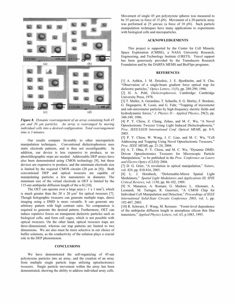
Since each cell of the array is an independent single particle trap, the array has the capability of being dynamically rearranged. To illustrate, an array consisting of 45 µm and 20 µm polystyrene spheres are reorganized under operator control (Fig. 8). This demonstrates the addressability of each particle trap, as well as the dynamic nature of the OET patterns.
Figure 5. Single-particle manipulation within thparticle in the lower-left side of the array is made array by combining cells (a), the re-splitting the celparticle to the adjacent array position (b).
acent cells, ed by first s illustrated in Fig. 5. The adjacent cells are me
removing the dividing wall, and then re-separating tmovement of the trap walls are controlled in real operator. To improve on the speed of this techniqlight wall can be used to
moving the particle nsferred to
en adjacent
n the array e variety of mming. For array, we ing
Figure 7. An array of single particlsingle particle square traps. Eachaddressable. The time required to formwas 3 minutes.
DISCUSSION
100 µm100 µm etween cells. This enables a single particle to be any cell of the array, using repeated transfers betwcells.
Since the patterns for manipulating the particlesare created dynamically by optical illumination, a woperations can be performed by simple software progrexample, to flush the particles in a single row of tremove the dividing walls of that row and use a mosweep ou
wall to
be formed positioned performed Point. The array of
Movement of a single 45-µm sphera maximum velocity of approximacorresponds to an estimated force of 15Law. The maximum velocity of a 20-papproximately 25 µm/sec. Thus, the meach individual array cell is 10 pN. Texperienced by a single 45 µm particle, probably
es, formed from multiple particle is individually this array of 20 particles
e due to negative DEP has tely 35 µm/sec. This pN, based upon Stoke’s article array is limited to inimum holding force of
his force is less than that due to slight non-
uniformities in image sharpness over the entire array area. The more defocused areas will have less of an electric field gradient, and a correspondingly lower DEP force. Thus, this 10 pN force reflects the minimum trapping force of all of the array cells.
The forces attained in these experiments, using an optical power density of 12 W/cm2, are in rough agreement with our earlier results using a 632-nm laser light source [4]. Our earlier data suggests that the optical power density necessary to achieve a force of 15 pN is 6.6 W/cm2. The difference between this predicted power density requirement and our experimental findings can be attributed to losses through the additional optics needed for our current experiment.
In addition to self-organizing behavior, arrays cfrom multiple single-particle traps. Each randomlyparticle is first contained within a square trap. This by drawing a rectangle around each particle in Powmultiple traps can then b
100 µmt = 0 min 100 µmt = 0 min 100 µmt = 1 min 100 µmt = 1 min (a) (b)
100 µm100 µm t = 3 mint = 3 min t = 2 mint = 2 min 100 µm100 µm
[3] T. Muller, A. Gerardino, T. Schnelle,G. Degasperis, R. Leoni, and G. Fuhr,
(c) (d)
n a
hgu
ve to produ
9]le c
ammited by the
mm2), which tweezers [7].
Though holographic tweezers can generate multiple traps, direct imaging using versatile. It can generate any arbitrary pattern with high contrast ratio. No computation is
e, OET can cles such as
with ers traps are
three-dimensional, whereas our trap patterns are limited to two dimensions. We are also must be more selective in our choice of buffer solutions, as the conductivity of the solution plays a crucial role in the DEP phenomenon.
CONCLUSIONS We have demonstrated the self-organizing of 45-um
polystyrene particles into an array, and the creation of an array from multiple single particle traps utilizing optoelectronics tweezers. Single particle movement within the array has been demonstrated, showing the ability to address individual array cells.
spheres was measured to ent of a 20-particle array
f 10 pN). Such particle iques have many applications to experiments
microparticles.
ENTS
Center for Cell Mimetic ASA University Research,
Engineering, and Technology Institute (URETI). Travel support has sly provided by the Transducers Research
nd BioFlips programs.
CES
Bjorkholm, and S. Chu, nt force optical trap for ), pp. 288-290, 1986.
University Press, 1978. S. G. Shirley, F. Bordoni, “Trapping of micrometer
and sub-micrometer particles by high-frequency electric fields and pplied Physics, 29(2), pp.
nd M. C. Wu, “A Novel uced Dielectrophoresis,”
Optical MEMS, pp. 8-9,
. Chiou, W. Wong, J. C. Liao, and M. C. Wu, “Cell ptoelectronic Tweezers,”
Chiou, and M. C. Wu, “Dynamic DMD-r Microscopic Particle
roc. Conference on Lasers
[7] D. G. Grier, “A revolution in optical manipulation,” Nature,
ormable-Mirror Spatial Light Modulators,” Spatial Light Modulators and Applications III, SPIE Critical Reviews, vol. 1150, pp. 86-102, 1989. [9] N. Manaresi, A. Romani, G. Medoro, L. Altomare, A. Leonardi, M. Tartagni, R. Guerrieri, “A CMOS Chip for Individual Cell Manipulation and Detection,” Proceedings of IEEE International Solid-State Circuits Conference 2003, vol. 1, pp. 192-487, 2003. [10] R. Schwarz, F. Wang, M. Reissner. “Fermi-level dependence of the ambipolar diffusion length in amorphous silicon thin film transistors,” Applied Physics Letters, vol. 63, p.1083, 1993.
Figure 8. Dynamic rearrangement of an array contaiµm and 20 µm particles. An array is rearrangedindividual cells into a desired configuration. Total retime is 3 minutes.
Our results compare favorably to other m
manipulation techniques. Conventional dielectropstatic electrode patterns, and is thus not reconfiaddition, our device is less expensi
ing both 45
hydrodynamic forces,” J. Physics D – A340-349, 1996.
by moving rrangement
[4] P. Y. Chiou, Z. Chang, Zehao, aOptoelectronic Tweezer Using Light IndProc. IEEE/LEOS International Conf. 2003.
icroparticle oresis uses rable. In
Addressing and Trapping Using Novel OProc. IEEE MEMS, pp. 21-24, 2004. [6] A. T. Ohta, P. Y.
ce, as no arrays have , but these ctrode size
Driven Optoelectronics Tweezers foManipulation,” to be published in the Pand Electro Optics (CLEO) 2004.
photolithographic steps are needed. Addressable DEPalso been demonstrated using CMOS technology [devices are expensive to produce, and the minimum eis limited by the required CMOS circuits (20 µm inconventional DEP and optical tweezers are manipulating particles a few nanometers in diminimum size of the virtual electrode in OET is li115-nm ambipolar diffusion length of the a-Si [10].
The OET can operate over a large area (~ 1 x 1is much greater than the 20 x 20 µm2 for optical
[9]). Both apable of eter. The
vol. 424, pp. 810-816, 2003. [8] L. J. Hornbeck, “Def
a DMD is more
required to generate the desired pattern. Furthermorinduce repulsive forces on transparent dielectric partibiological cells, and form cell cages, which is not possible optical tweezers. On the other hand, optical tweez
Movement of single 45 µm polystyrenebe 35 µm/sec (a force of 15 pN). Movemwas performed at 25 µm/sec (a force omanipulation technwith biological cells and
ACKNOWLEDGEM This project is supported by the
Space Exploration (CMISE), a N
been generouFoundation and by the DARPA MEMS a
REFEREN [1] A. Ashkin, J. M. Dziedzic, J. E. “Observation of a single-beam gradiedielectric particles,” Optics Letters, 11(5[2] H. A. Pohl, Dielectrophoresis. Cambridge: Cambridge
[5] P. Y