Dual Very Low Noise Precision Operational Amplifier Data ...
21
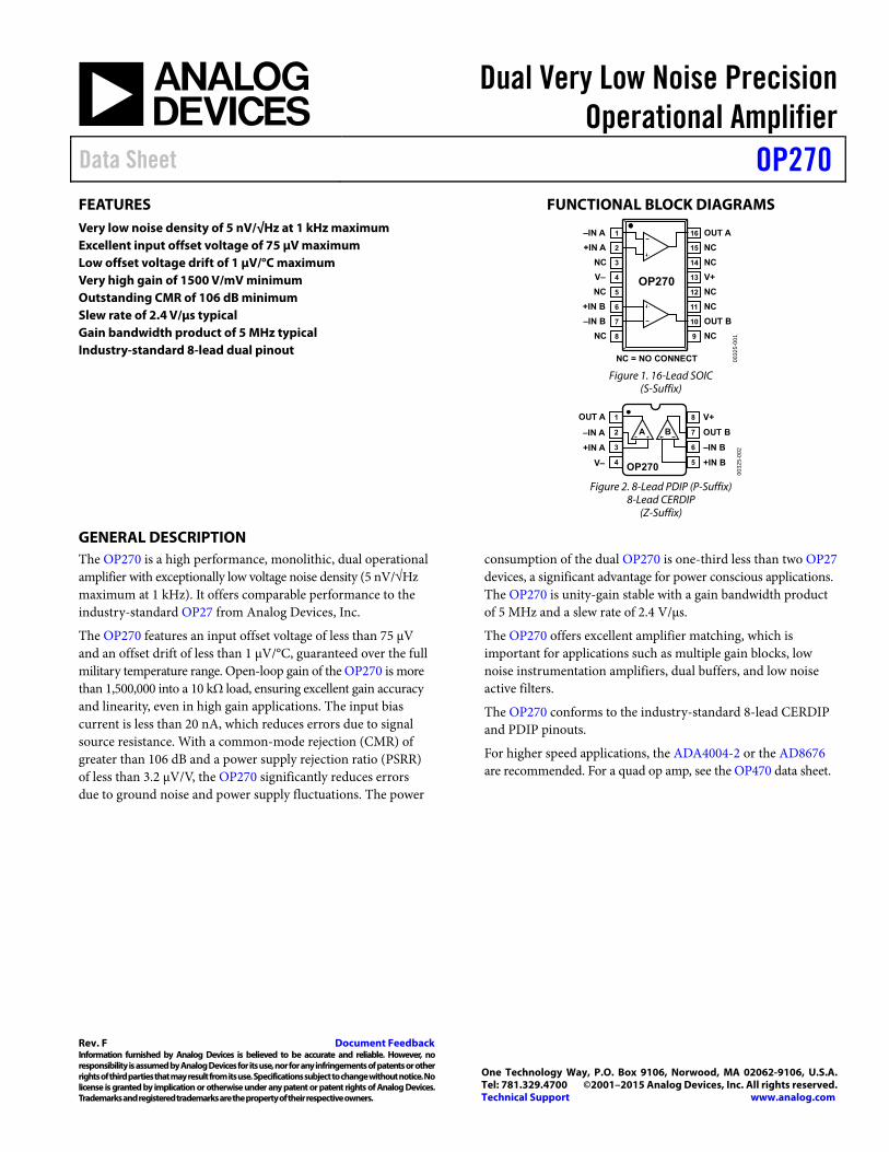
Dual Very Low Noise Precision Operational Amplifier Data Sheet OP270 Rev. F Document Feedback Information furnished by Analog Devices is believed to be accurate and reliable. However, no responsibility is assumed by Analog Devices for its use, nor for any infringements of patents or other rights of third parties that may result from its use. Specifications subject to change without notice. No license is granted by implication or otherwise under any patent or patent rights of Analog Devices. Trademarks and registered trademarks are the property of their respective owners. One Technology Way, P.O. Box 9106, Norwood, MA 02062-9106, U.S.A. Tel: 781.329.4700 ©2001–2015 Analog Devices, Inc. All rights reserved. Technical Support www.analog.com FEATURES Very low noise density of 5 nV/√Hz at 1 kHz maximum Excellent input offset voltage of 75 μV maximum Low offset voltage drift of 1 μV/°C maximum Very high gain of 1500 V/mV minimum Outstanding CMR of 106 dB minimum Slew rate of 2.4 V/μs typical Gain bandwidth product of 5 MHz typical Industry-standard 8-lead dual pinout FUNCTIONAL BLOCK DIAGRAMS 00325-001 –IN A 1 +IN A 2 NC 3 V– 4 OUT A 16 NC 15 NC 14 V+ 13 NC 5 NC 12 +IN B 6 NC 11 –IN B 7 OUT B 10 NC 8 NC 9 NC = NO CONNECT OP270 Figure 1. 16-Lead SOIC (S-Suffix) 00325-002 OP270 OUT A A B 1 –IN A 2 +IN A 3 V– 4 V+ 8 OUT B 7 –IN B 6 +IN B 5 Figure 2. 8-Lead PDIP (P-Suffix) 8-Lead CERDIP (Z-Suffix) GENERAL DESCRIPTION The OP270 is a high performance, monolithic, dual operational amplifier with exceptionally low voltage noise density (5 nV/√Hz maximum at 1 kHz). It offers comparable performance to the industry-standard OP27 from Analog Devices, Inc. The OP270 features an input offset voltage of less than 75 μV and an offset drift of less than 1 μV/°C, guaranteed over the full military temperature range. Open-loop gain of the OP270 is more than 1,500,000 into a 10 kΩ load, ensuring excellent gain accuracy and linearity, even in high gain applications. The input bias current is less than 20 nA, which reduces errors due to signal source resistance. With a common-mode rejection (CMR) of greater than 106 dB and a power supply rejection ratio (PSRR) of less than 3.2 μV/V, the OP270 significantly reduces errors due to ground noise and power supply fluctuations. The power consumption of the dual OP270 is one-third less than two OP27 devices, a significant advantage for power conscious applications. The OP270 is unity-gain stable with a gain bandwidth product of 5 MHz and a slew rate of 2.4 V/μs. The OP270 offers excellent amplifier matching, which is important for applications such as multiple gain blocks, low noise instrumentation amplifiers, dual buffers, and low noise active filters. The OP270 conforms to the industry-standard 8-lead CERDIP and PDIP pinouts. For higher speed applications, the ADA4004-2 or the AD8676 are recommended. For a quad op amp, see the OP470 data sheet.
Transcript of Dual Very Low Noise Precision Operational Amplifier Data ...
Dual Very Low Noise Precision Operational Amplifier
Data Sheet OP270
Rev. F Document Feedback Information furnished by Analog Devices is believed to be accurate and reliable. However, no responsibility is assumed by Analog Devices for its use, nor for any infringements of patents or other rights of third parties that may result from its use. Specifications subject to change without notice. No license is granted by implication or otherwise under any patent or patent rights of Analog Devices. Trademarks and registered trademarks are the property of their respective owners.
One Technology Way, P.O. Box 9106, Norwood, MA 02062-9106, U.S.A.Tel: 781.329.4700 ©2001–2015 Analog Devices, Inc. All rights reserved. Technical Support www.analog.com
FEATURES Very low noise density of 5 nV/√Hz at 1 kHz maximum Excellent input offset voltage of 75 μV maximum Low offset voltage drift of 1 μV/°C maximum Very high gain of 1500 V/mV minimum Outstanding CMR of 106 dB minimum Slew rate of 2.4 V/μs typical Gain bandwidth product of 5 MHz typical Industry-standard 8-lead dual pinout
FUNCTIONAL BLOCK DIAGRAMS
0032
5-00
1
–IN A 1
+IN A 2
NC 3
V– 4
OUT A16
NC15
NC14
V+13
NC 5 NC12
+IN B 6 NC11
–IN B 7 OUT B10
NC 8 NC9
NC = NO CONNECT
OP270
Figure 1. 16-Lead SOIC
(S-Suffix)
0032
5-00
2
OP270
OUT A
A B
1
–IN A 2
+IN A 3
V– 4
V+8
OUT B7
–IN B6
+IN B5
Figure 2. 8-Lead PDIP (P-Suffix)
8-Lead CERDIP (Z-Suffix)
GENERAL DESCRIPTION The OP270 is a high performance, monolithic, dual operational amplifier with exceptionally low voltage noise density (5 nV/√Hz maximum at 1 kHz). It offers comparable performance to the industry-standard OP27 from Analog Devices, Inc.
The OP270 features an input offset voltage of less than 75 μV and an offset drift of less than 1 μV/°C, guaranteed over the full military temperature range. Open-loop gain of the OP270 is more than 1,500,000 into a 10 kΩ load, ensuring excellent gain accuracy and linearity, even in high gain applications. The input bias current is less than 20 nA, which reduces errors due to signal source resistance. With a common-mode rejection (CMR) of greater than 106 dB and a power supply rejection ratio (PSRR) of less than 3.2 μV/V, the OP270 significantly reduces errors due to ground noise and power supply fluctuations. The power
consumption of the dual OP270 is one-third less than two OP27 devices, a significant advantage for power conscious applications. The OP270 is unity-gain stable with a gain bandwidth product of 5 MHz and a slew rate of 2.4 V/μs.
The OP270 offers excellent amplifier matching, which is important for applications such as multiple gain blocks, low noise instrumentation amplifiers, dual buffers, and low noise active filters.
The OP270 conforms to the industry-standard 8-lead CERDIP and PDIP pinouts.
For higher speed applications, the ADA4004-2 or the AD8676 are recommended. For a quad op amp, see the OP470 data sheet.
OP270* PRODUCT PAGE QUICK LINKSLast Content Update: 02/23/2017
COMPARABLE PARTSView a parametric search of comparable parts.
DOCUMENTATIONApplication Notes
• AN-649: Using the Analog Devices Active Filter Design Tool
• AN-940: Low Noise Amplifier Selection Guide for Optimal Noise Performance
Data Sheet
• OP270: Dual Very Low Noise Precision Operational Amplifier Data Sheet
TOOLS AND SIMULATIONS• OP270 SPICE Macro Model
DESIGN RESOURCES• OP270 Material Declaration
• PCN-PDN Information
• Quality And Reliability
• Symbols and Footprints
DISCUSSIONSView all OP270 EngineerZone Discussions.
SAMPLE AND BUYVisit the product page to see pricing options.
TECHNICAL SUPPORTSubmit a technical question or find your regional support number.
DOCUMENT FEEDBACKSubmit feedback for this data sheet.
This page is dynamically generated by Analog Devices, Inc., and inserted into this data sheet. A dynamic change to the content on this page will not trigger a change to either the revision number or the content of the product data sheet. This dynamic page may be frequently modified.
OP270 Data Sheet
Rev. F | Page 2 of 20
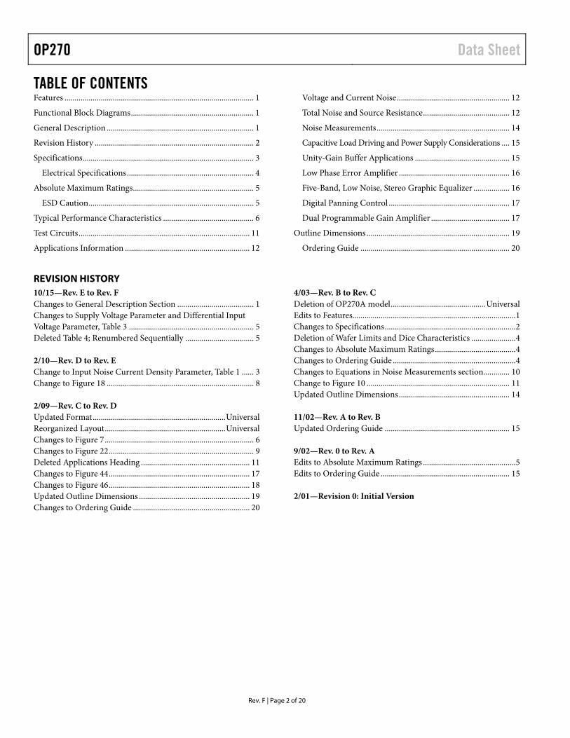
TABLE OF CONTENTS Features .............................................................................................. 1
Functional Block Diagrams ............................................................. 1
General Description ......................................................................... 1
Revision History ............................................................................... 2
Specifications ..................................................................................... 3
Electrical Specifications ............................................................... 4
Absolute Maximum Ratings ............................................................ 5
ESD Caution .................................................................................. 5
Typical Performance Characteristics ............................................. 6
Test Circuits ..................................................................................... 11
Applications Information .............................................................. 12
Voltage and Current Noise ........................................................ 12
Total Noise and Source Resistance ........................................... 12
Noise Measurements .................................................................. 14
Capacitive Load Driving and Power Supply Considerations .... 15
Unity-Gain Buffer Applications ............................................... 15
Low Phase Error Amplifier ....................................................... 16
Five-Band, Low Noise, Stereo Graphic Equalizer .................. 16
Digital Panning Control ............................................................ 17
Dual Programmable Gain Amplifier ....................................... 17
Outline Dimensions ....................................................................... 19
Ordering Guide .......................................................................... 20
REVISION HISTORY 10/15—Rev. E to Rev. F Changes to General Description Section ...................................... 1 Changes to Supply Voltage Parameter and Differential Input Voltage Parameter, Table 3 .............................................................. 5 Deleted Table 4; Renumbered Sequentially .................................. 5 2/10—Rev. D to Rev. E Change to Input Noise Current Density Parameter, Table 1 ...... 3 Change to Figure 18 ......................................................................... 8 2/09—Rev. C to Rev. D Updated Format .................................................................. Universal Reorganized Layout ............................................................ Universal Changes to Figure 7 .......................................................................... 6 Changes to Figure 22 ........................................................................ 9 Deleted Applications Heading ...................................................... 11 Changes to Figure 44 ...................................................................... 17 Changes to Figure 46 ...................................................................... 18 Updated Outline Dimensions ....................................................... 19 Changes to Ordering Guide .......................................................... 20
4/03—Rev. B to Rev. C Deletion of OP270A model ............................................... Universal Edits to Features ................................................................................. 1 Changes to Specifications ................................................................. 2 Deletion of Wafer Limits and Dice Characteristics ...................... 4 Changes to Absolute Maximum Ratings ........................................ 4 Changes to Ordering Guide ............................................................. 4 Changes to Equations in Noise Measurements section ............. 10 Change to Figure 10 ....................................................................... 11 Updated Outline Dimensions ....................................................... 14 11/02—Rev. A to Rev. B Updated Ordering Guide .............................................................. 15 9/02—Rev. 0 to Rev. A Edits to Absolute Maximum Ratings .............................................. 5 Edits to Ordering Guide ................................................................ 15 2/01—Revision 0: Initial Version
Data Sheet OP270
Rev. F | Page 3 of 20
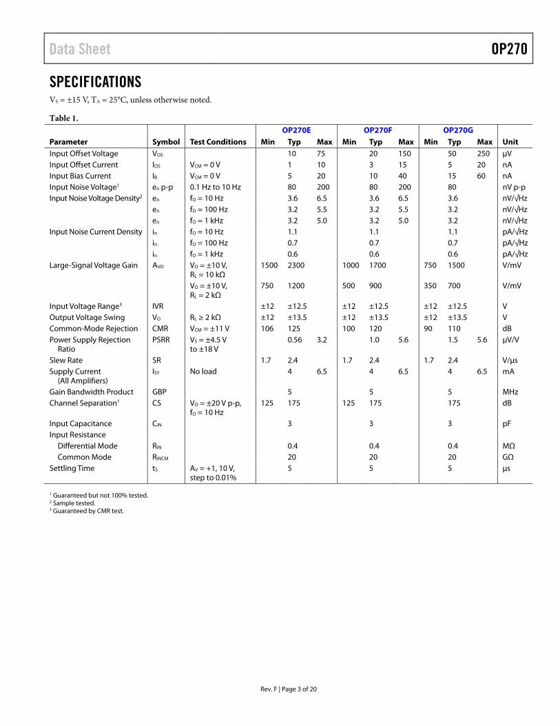
SPECIFICATIONS VS = ±15 V, TA = 25°C, unless otherwise noted.
Table 1.
Parameter Symbol Test Conditions OP270E OP270F OP270G
Unit Min Typ Max Min Typ Max Min Typ Max Input Offset Voltage VOS 10 75 20 150 50 250 μV Input Offset Current IOS VCM = 0 V 1 10 3 15 5 20 nA Input Bias Current IB VCM = 0 V 5 20 10 40 15 60 nA Input Noise Voltage1 en p-p 0.1 Hz to 10 Hz 80 200 80 200 80 nV p-p Input Noise Voltage Density2 en fO = 10 Hz 3.6 6.5 3.6 6.5 3.6 nV/√Hz
en fO = 100 Hz 3.2 5.5 3.2 5.5 3.2 nV/√Hz en fO = 1 kHz 3.2 5.0 3.2 5.0 3.2 nV/√Hz Input Noise Current Density in fO = 10 Hz 1.1 1.1 1.1 pA/√Hz
in fO = 100 Hz 0.7 0.7 0.7 pA/√Hz in fO = 1 kHz 0.6 0.6 0.6 pA/√Hz Large-Signal Voltage Gain AVO VO = ±10 V,
RL = 10 kΩ 1500 2300 1000 1700 750 1500 V/mV
VO = ±10 V, RL = 2 kΩ
750 1200 500 900 350 700 V/mV
Input Voltage Range3 IVR ±12 ±12.5 ±12 ±12.5 ±12 ±12.5 V Output Voltage Swing VO RL ≥ 2 kΩ ±12 ±13.5 ±12 ±13.5 ±12 ±13.5 V Common-Mode Rejection CMR VCM = ±11 V 106 125 100 120 90 110 dB Power Supply Rejection
Ratio PSRR VS = ±4.5 V
to ±18 V 0.56 3.2 1.0 5.6 1.5 5.6 μV/V
Slew Rate SR 1.7 2.4 1.7 2.4 1.7 2.4 V/μs Supply Current
(All Amplifiers) ISY No load 4 6.5 4 6.5 4 6.5 mA
Gain Bandwidth Product GBP 5 5 5 MHz Channel Separation1 CS VO = ±20 V p-p,
fO = 10 Hz 125 175 125 175 175 dB
Input Capacitance CIN 3 3 3 pF Input Resistance
Differential Mode RIN 0.4 0.4 0.4 MΩ Common Mode RINCM 20 20 20 GΩ
Settling Time tS AV = +1, 10 V, step to 0.01%
5 5 5 μs
1 Guaranteed but not 100% tested. 2 Sample tested. 3 Guaranteed by CMR test.
OP270 Data Sheet
Rev. F | Page 4 of 20
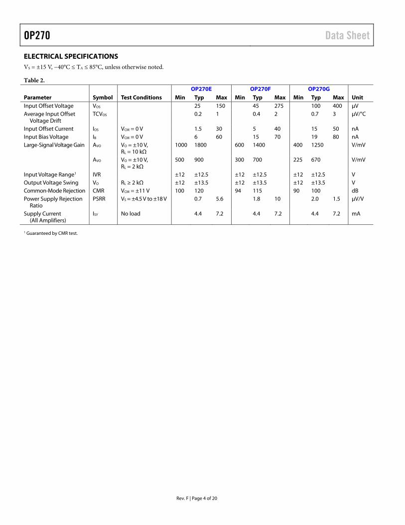
ELECTRICAL SPECIFICATIONS VS = ±15 V, −40°C ≤ TA ≤ 85°C, unless otherwise noted.
Table 2.
Parameter Symbol Test Conditions OP270E OP270F OP270G
Unit Min Typ Max Min Typ Max Min Typ Max Input Offset Voltage VOS 25 150 45 275 100 400 μV Average Input Offset
Voltage Drift TCVOS 0.2 1 0.4 2 0.7 3 μV/°C
Input Offset Current IOS VCM = 0 V 1.5 30 5 40 15 50 nA Input Bias Voltage IB VCM = 0 V 6 60 15 70 19 80 nA Large-Signal Voltage Gain AVO VO = ±10 V,
RL = 10 kΩ 1000 1800 600 1400 400 1250 V/mV
AVO VO = ±10 V, RL = 2 kΩ
500 900 300 700 225 670 V/mV
Input Voltage Range1 IVR ±12 ±12.5 ±12 ±12.5 ±12 ±12.5 V Output Voltage Swing VO RL ≥ 2 kΩ ±12 ±13.5 ±12 ±13.5 ±12 ±13.5 V Common-Mode Rejection CMR VCM = ±11 V 100 120 94 115 90 100 dB Power Supply Rejection
Ratio PSRR VS = ±4.5 V to ±18 V 0.7 5.6 1.8 10 2.0 1.5 μV/V
Supply Current (All Amplifiers)
ISY No load 4.4 7.2 4.4 7.2 4.4 7.2 mA
1 Guaranteed by CMR test.
Data Sheet OP270
Rev. F | Page 5 of 20
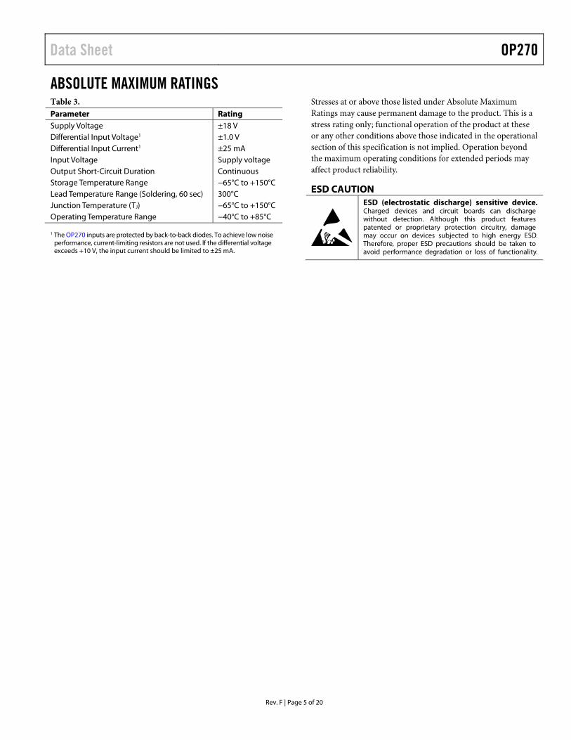
ABSOLUTE MAXIMUM RATINGS Table 3. Parameter Rating Supply Voltage ±18 V Differential Input Voltage1 ±1.0 V Differential Input Current1 ±25 mA Input Voltage Supply voltage Output Short-Circuit Duration Continuous Storage Temperature Range −65°C to +150°C Lead Temperature Range (Soldering, 60 sec) 300°C Junction Temperature (TJ) −65°C to +150°C Operating Temperature Range −40°C to +85°C
1 The OP270 inputs are protected by back-to-back diodes. To achieve low noise performance, current-limiting resistors are not used. If the differential voltage exceeds +10 V, the input current should be limited to ±25 mA.
Stresses at or above those listed under Absolute Maximum Ratings may cause permanent damage to the product. This is a stress rating only; functional operation of the product at these or any other conditions above those indicated in the operational section of this specification is not implied. Operation beyond the maximum operating conditions for extended periods may affect product reliability.
ESD CAUTION
OP270 Data Sheet
Rev. F | Page 6 of 20
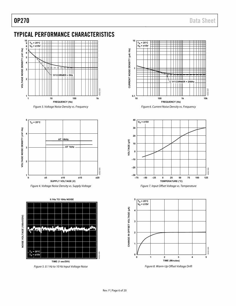
TYPICAL PERFORMANCE CHARACTERISTICS
0035
2-00
4
10
3
4
5
6
789
2
11 10 100 1k
VO
LT
AG
E N
OIS
E D
EN
SIT
Y (
nV
/√H
z)
FREQUENCY (Hz)
TA = 25°CVS = ±15V
1/f CORNER = 5Hz
Figure 3. Voltage Noise Density vs. Frequency
0035
2-00
5
5
3
4
2
10 ±5 ±10 ±15 ±20
VO
LT
AG
E N
OIS
E D
EN
SIT
Y (
nV
/√H
z)
SUPPLY VOLTAGE (V)
TA = 25°C
AT 1kHz
AT 10kHz
Figure 4. Voltage Noise Density vs. Supply Voltage
0035
2-00
6
NO
ISE
VO
LT
AG
E (
100n
V/D
IV)
TIME (1 sec/DIV)
0.1Hz TO 10Hz NOISE
TA = 25°CTS = ±15V
Figure 5. 0.1 Hz to 10 Hz Input Voltage Noise
0035
2-00
7
10
1
0.110 100 1k 10k
CU
RR
EN
T N
OIS
E D
EN
SIT
Y (
pA
/√H
z)
FREQUENCY (Hz)
TA = 25°CVS = ±15V
1/f CORNER = 200Hz
Figure 6. Current Noise Density vs. Frequency
0035
2-00
8
40
0
10
20
30
–30
–20
–10
–75 –50 –25 25 50 75 100 1250
VO
LT
AG
E (
µV
)
TEMPERATURE (°C)
VS = ±15V
Figure 7. Input Offset Voltage vs. Temperature
0035
2-00
9
5
4
0
1
2
3
0 2 3 4 51
CH
AN
GE
IN
OF
FS
ET
VO
LT
AG
E (
µA
)
TIME (Minutes)
TA = 25°CVS = ±15V
Figure 8. Warm-Up Offset Voltage Drift
Data Sheet OP270
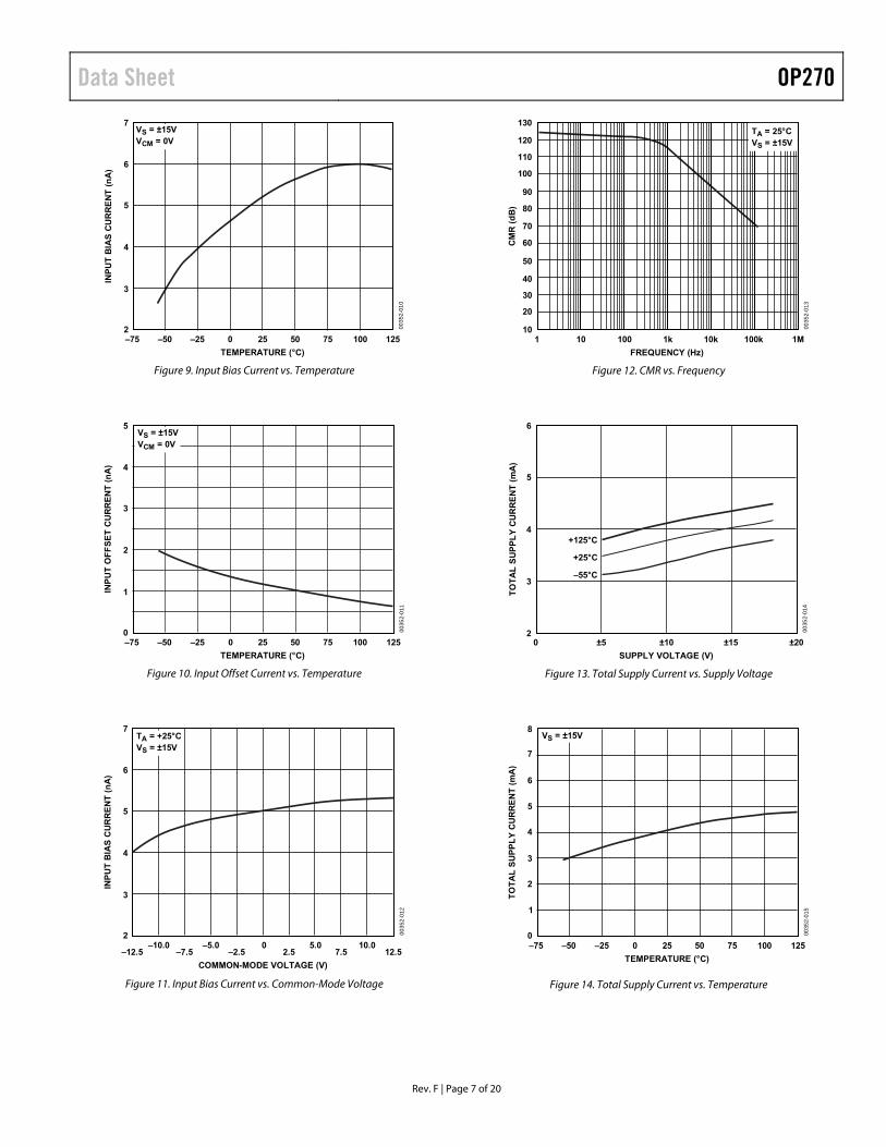
Rev. F | Page 7 of 20
0035
2-01
0
7
6
2
3
4
5
INP
UT
BIA
S C
UR
RE
NT
(n
A)
TEMPERATURE (°C)
VS = ±15VVCM = 0V
–75 –50 –25 25 50 75 100 1250
Figure 9. Input Bias Current vs. Temperature
0035
2-01
1
5
4
0
1
2
3
INP
UT
OF
FS
ET
CU
RR
EN
T (
nA
)
TEMPERATURE (°C)
VS = ±15VVCM = 0V
–75 –50 –25 25 50 75 100 1250
Figure 10. Input Offset Current vs. Temperature
0035
2-01
2
7
6
2
3
4
5
INP
UT
BIA
S C
UR
RE
NT
(n
A)
COMMON-MODE VOLTAGE (V)
–12.5 –7.5 –2.5 2.5–10.0 –5.0 0 5.0
7.5 12.510.0
TA = +25°CVS = ±15V
Figure 11. Input Bias Current vs. Common-Mode Voltage
0035
2-01
3
130
100
110
120
10
20
30
40
50
60
70
80
90
CM
R (
dB
)
FREQUENCY (Hz)
1 10 1k 10k 100k 1M100
TA = 25°CVS = ±15V
Figure 12. CMR vs. Frequency
0035
2-01
4
6
4
5
3
20 ±5 ±10 ±15 ±20
TO
TA
L S
UP
PL
Y C
UR
RE
NT
(m
A)
SUPPLY VOLTAGE (V)
+125°C
+25°C
–55°C
Figure 13. Total Supply Current vs. Supply Voltage
0035
2-01
5
8
7
2
1
0
3
4
5
6
TO
TA
L S
UP
PL
Y C
UR
RE
NT
(m
A)
TEMPERATURE (°C)
VS = ±15V
–75 –50 –25 25 50 75 100 1250
Figure 14. Total Supply Current vs. Temperature
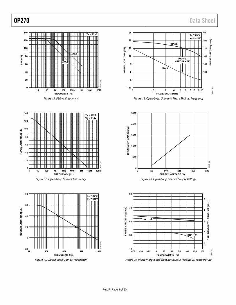
OP270 Data Sheet
Rev. F | Page 8 of 20
0035
2-01
6
140
100
120
0
20
40
60
80
PS
R (
dB
)
FREQUENCY (Hz)
1 10 1k 10k 100k 1M 10M 100M100
TA = 25°C
–PSR
+PSR
Figure 15. PSR vs. Frequency 00
352-
017
140
100
120
0
20
40
60
80
OP
EN
-LO
OP
GA
IN (
dB
)
FREQUENCY (Hz)
1 10 1k 10k 100k 1M 10M 100M100
TA = 25°CVS = ±15V
Figure 16. Open-Loop Gain vs. Frequency
0035
2-01
8
80
60
–20
0
20
40
CL
OS
ED
-LO
OP
GA
IN (
dB
)
FREQUENCY (Hz)
1k 10k 100k 1M 10M
TA = 25°CVS = ±15V
Figure 17. Closed-Loop Gain vs. Frequency
0035
2-01
9
25
15
20
–10
–5
0
5
10
OP
EN
-LO
OP
GA
IN (
dB
)
FREQUENCY (MHz)
1 2 3 4 5 6 7 8 9 10
TA = 25°CVS = ±15V
PH
AS
E S
HIF
T (
Deg
rees
)
180
160
140
120
100
80
PHASEMARGIN = 62°
GAIN
PHASE
Figure 18. Open-Loop Gain and Phase Shift vs. Frequency
0035
2-02
0
5000
1000
2000
3000
4000
00 ±5 ±10 ±15 ±20 ±25
OP
EN
-LO
OP
GA
IN (
V/m
A)
SUPPLY VOLTAGE (V)
Figure 19. Open-Loop Gain vs. Supply Voltage
0035
2-02
1
80
70
40
50
60
PH
AS
E M
AR
GIN
(D
egre
es)
TEMPERATURE (°C)
–75 –50 –25 25 50 75 100 125 1500
GA
IN B
AN
DW
IDT
H P
RO
DU
CT
(M
Hz)
4
5
6
7
8
GBP
Ф
Figure 20. Phase Margin and Gain Bandwidth Product vs. Temperature
Data Sheet OP270
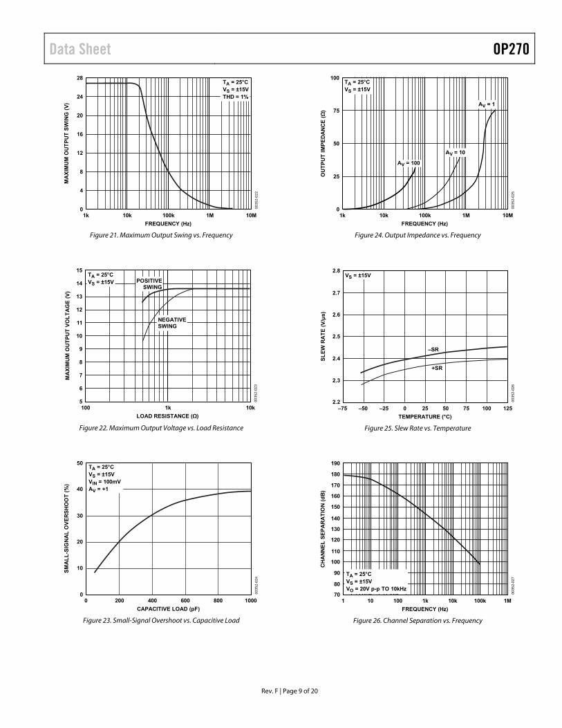
Rev. F | Page 9 of 20
0035
2-02
2
28
20
24
0
4
8
12
16
MA
XIM
UM
OU
TP
UT
SW
ING
(V
)
FREQUENCY (Hz)
1k 10k 100k 1M 10M
TA = 25°CVS = ±15VTHD = 1%
Figure 21. Maximum Output Swing vs. Frequency
0035
2-02
3
15
12
13
14
5
6
7
8
9
10
11
MA
XIM
UM
OU
TP
UT
VO
LT
AG
E (
V)
LOAD RESISTANCE (Ω)
100 1k 10k
TA = 25°CVS = ±15V POSITIVE
SWING
NEGATIVESWING
Figure 22. Maximum Output Voltage vs. Load Resistance
0035
2-02
4
50
40
0
10
20
30
SM
AL
L-S
IGN
AL
OV
ER
SH
OO
T (
%)
CAPACITIVE LOAD (pF)
0 200 400 600 800 1000
TA = 25°CVS = ±15VVIN = 100mVAV = +1
Figure 23. Small-Signal Overshoot vs. Capacitive Load
0035
2-02
5
100
75
0
25
50
OU
TP
UT
IM
PE
DA
NC
E (Ω
)
FREQUENCY (Hz)
1k 10k 100k 1M 10M
TA = 25°CVS = ±15V
AV = 100
AV = 10
AV = 1
Figure 24. Output Impedance vs. Frequency
0035
2-02
6
2.2
2.3
2.4
2.5
2.6
2.7
2.8
SL
EW
RA
TE
(V
/µs)
TEMPERATURE (°C)
VS = ±15V
–75 –50 –25 25 50 75 100 1250
–SR
+SR
Figure 25. Slew Rate vs. Temperature
0035
2-02
7
190
150
160
170
180
70
80
90
100
110
120
130
140
CH
AN
NE
L S
EP
AR
AT
ION
(d
B)
FREQUENCY (Hz)
1 10 1k 10k 100k 1M100
TA = 25°CVS = ±15VVO = 20V p-p TO 10kHz
Figure 26. Channel Separation vs. Frequency
OP270 Data Sheet
Rev. F | Page 10 of 20
0035
2-02
8
0.1
0.01
0.00110 100 1k 10k
TO
TA
L H
AR
MO
NIC
DIS
TO
RT
ION
(%
)
FREQUENCY (Hz)
TA = 25°CVS = ±15VVO = 20V p-pRL = 2kΩ
AV = 10
AV = 1
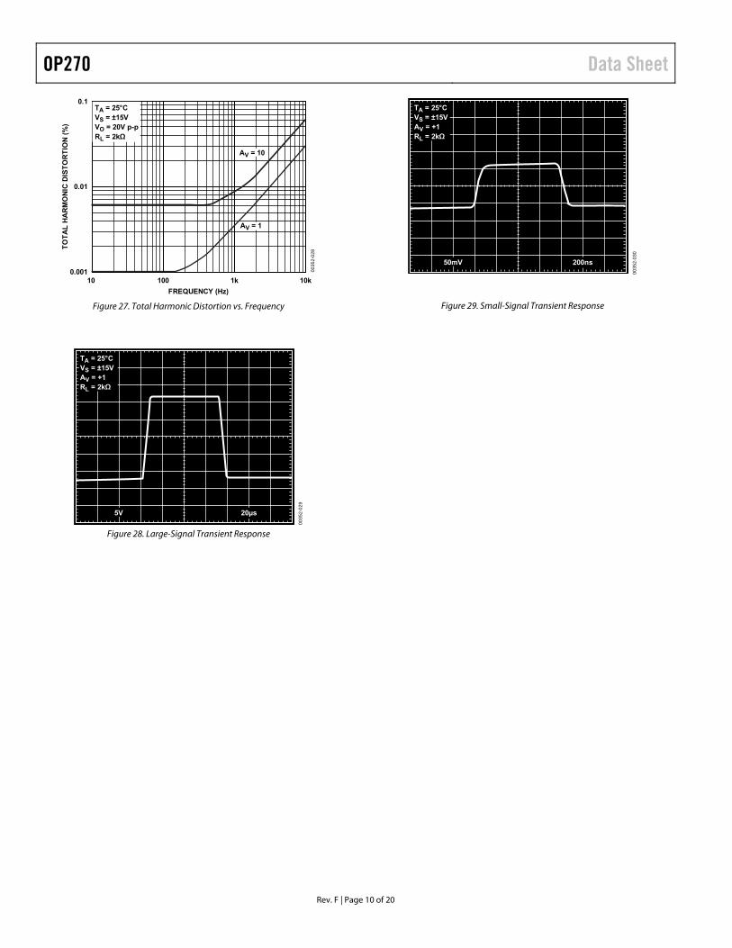
Figure 27. Total Harmonic Distortion vs. Frequency 00
352-
029
TA = 25°CVS = ±15VAV = +1RL = 2kΩ
5V 20µs
Figure 28. Large-Signal Transient Response
0035
2-03
0
TA = 25°CVS = ±15VAV = +1RL = 2kΩ
50mV 200ns
Figure 29. Small-Signal Transient Response
Data Sheet OP270
Rev. F | Page 11 of 20
TEST CIRCUITS
0032
5-03
1
1/2OP270
500Ω
5kΩ
V1 20Vp-p
1/2OP270
CHANNEL SEPARATION = 20 LOG
50Ω
5kΩ
V2
V1
V2/1000
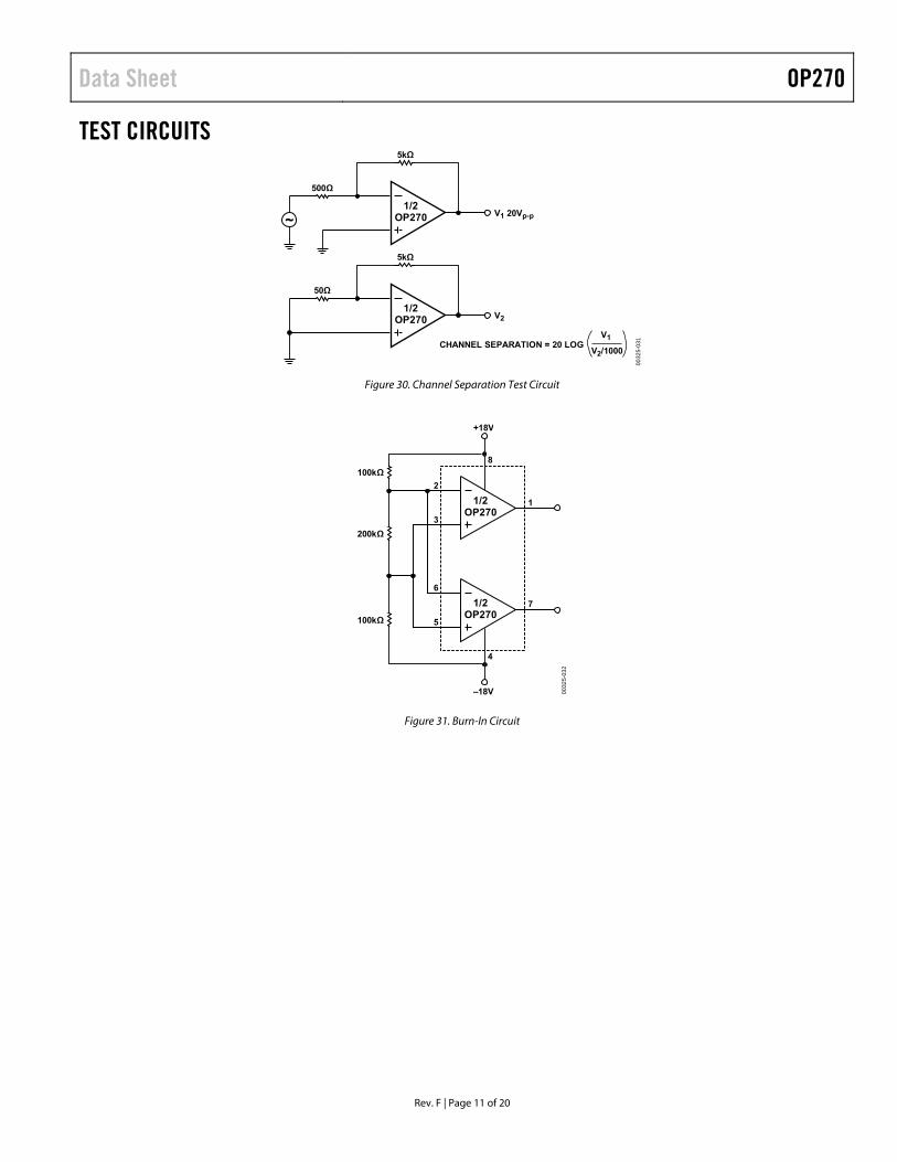
Figure 30. Channel Separation Test Circuit
0032
5-03
2
1/2OP270
100kΩ
1/2OP270
+18V
–18V
200kΩ
100kΩ
2
1
7
3
6
5
4
8
Figure 31. Burn-In Circuit
OP270 Data Sheet
Rev. F | Page 12 of 20
APPLICATIONS INFORMATION VOLTAGE AND CURRENT NOISE The OP270 is a very low noise dual op amp, exhibiting a typical voltage noise density of only 3.2 nV/√Hz at 1 kHz. Because the voltage noise is inversely proportional to the square root of the collector current, the exceptionally low noise characteristic of the OP270 is achieved in part by operating the input transistors at high collector currents. Current noise, however, is directly proportional to the square root of the collector current. As a result, the outstanding voltage noise density performance of the OP270 is gained at the expense of current noise performance, which is normal for low noise amplifiers.
To obtain the best noise performance in a circuit, it is vital to understand the relationships among voltage noise (en), current noise (in), and resistor noise (et).
TOTAL NOISE AND SOURCE RESISTANCE The total noise of an op amp can be calculated by
222 )()()( tsnnn eRieE
where: En is the total input-referred noise. en is the op amp voltage noise. in is the op amp current noise. et is the source resistance thermal noise. RS is the source resistance.
The total noise is referred to the input and at the output is amplified by the circuit gain.
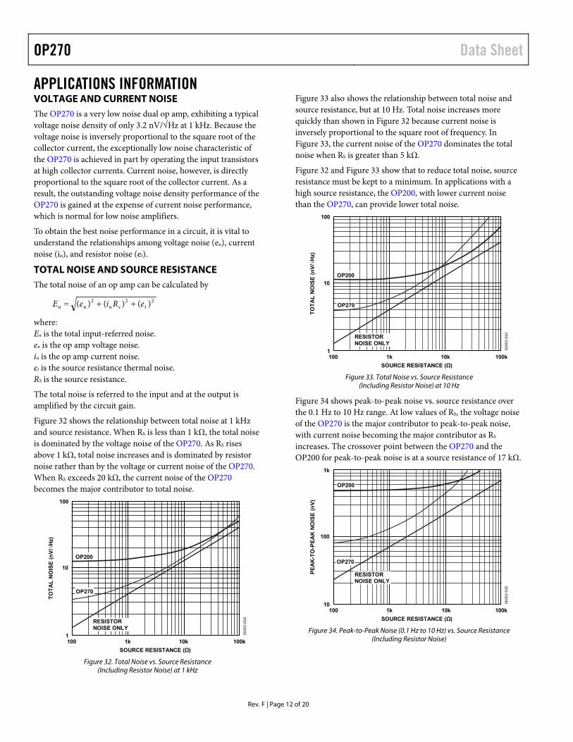
Figure 32 shows the relationship between total noise at 1 kHz and source resistance. When RS is less than 1 kΩ, the total noise is dominated by the voltage noise of the OP270. As RS rises above 1 kΩ, total noise increases and is dominated by resistor noise rather than by the voltage or current noise of the OP270. When RS exceeds 20 kΩ, the current noise of the OP270 becomes the major contributor to total noise.
0035
2-03
3
100
10
1100 1k 10k 100k
TO
TA
L N
OIS
E (
nV
/√H
z)
SOURCE RESISTANCE (Ω)
RESISTORNOISE ONLY
OP200
OP270
Figure 32. Total Noise vs. Source Resistance
(Including Resistor Noise) at 1 kHz
Figure 33 also shows the relationship between total noise and source resistance, but at 10 Hz. Total noise increases more quickly than shown in Figure 32 because current noise is inversely proportional to the square root of frequency. In Figure 33, the current noise of the OP270 dominates the total noise when RS is greater than 5 kΩ.
Figure 32 and Figure 33 show that to reduce total noise, source resistance must be kept to a minimum. In applications with a high source resistance, the OP200, with lower current noise than the OP270, can provide lower total noise.
0035
2-03
4
100
10
1100 1k 10k 100k
TO
TA
L N
OIS
E (
nV
/√H
z)
SOURCE RESISTANCE (Ω)
RESISTORNOISE ONLY
OP200
OP270
Figure 33. Total Noise vs. Source Resistance
(Including Resistor Noise) at 10 Hz
Figure 34 shows peak-to-peak noise vs. source resistance over the 0.1 Hz to 10 Hz range. At low values of RS, the voltage noise of the OP270 is the major contributor to peak-to-peak noise, with current noise becoming the major contributor as RS increases. The crossover point between the OP270 and the OP200 for peak-to-peak noise is at a source resistance of 17 kΩ.
0035
2-03
5
1k
100
10100 1k 10k 100k
PE
AK
-TO
-PE
AK
NO
ISE
(n
V)
SOURCE RESISTANCE (Ω)
RESISTORNOISE ONLY
OP200
OP270
Figure 34. Peak-to-Peak Noise (0.1 Hz to 10 Hz) vs. Source Resistance
(Including Resistor Noise)
Data Sheet OP270
Rev. F | Page 13 of 20
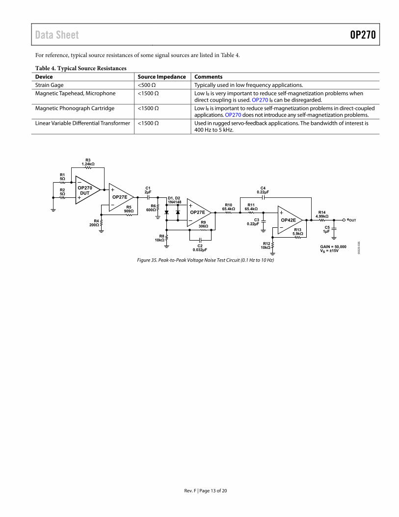
For reference, typical source resistances of some signal sources are listed in Table 4.
Table 4. Typical Source Resistances Device Source Impedance Comments Strain Gage <500 Ω Typically used in low frequency applications. Magnetic Tapehead, Microphone <1500 Ω Low IB is very important to reduce self-magnetization problems when
direct coupling is used. OP270 IB can be disregarded. Magnetic Phonograph Cartridge <1500 Ω Low IB is important to reduce self-magnetization problems in direct-coupled
applications. OP270 does not introduce any self-magnetization problems. Linear Variable Differential Transformer <1500 Ω Used in rugged servo-feedback applications. The bandwidth of interest is
400 Hz to 5 kHz.
0032
5-03
6
OP270DUT
R15Ω
R25Ω
R31.24kΩ
OP27E
R5909Ω
R4200Ω
R135.9kΩ
R1210kΩ
OP27E
OP42ER9306Ω
R1065.4kΩ
R1165.4kΩ
R810kΩ
C12µF
C40.22µF
D1, D21N4148
R6600Ω
C20.032µF
C30.22µF
C51µF
R144.99kΩ
eOUT
GAIN = 50,000VS = ±15V
Figure 35. Peak-to-Peak Voltage Noise Test Circuit (0.1 Hz to 10 Hz)
OP270 Data Sheet
Rev. F | Page 14 of 20
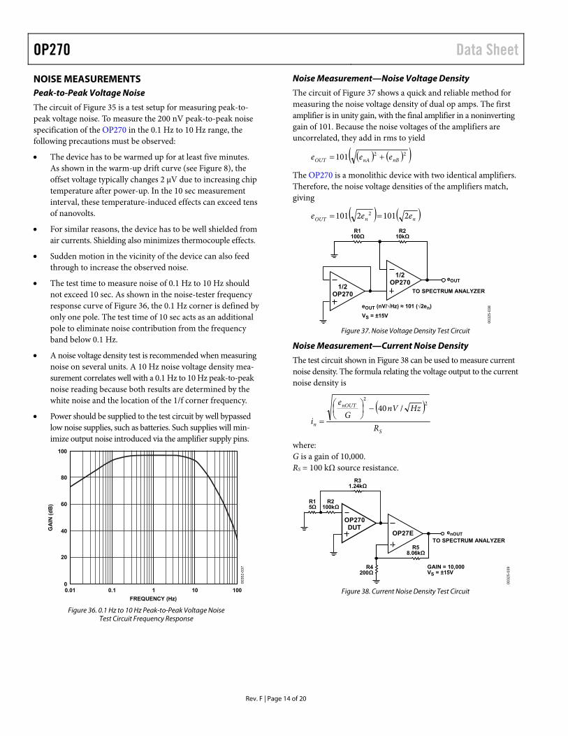
NOISE MEASUREMENTS Peak-to-Peak Voltage Noise
The circuit of Figure 35 is a test setup for measuring peak-to-peak voltage noise. To measure the 200 nV peak-to-peak noise specification of the OP270 in the 0.1 Hz to 10 Hz range, the following precautions must be observed:
The device has to be warmed up for at least five minutes. As shown in the warm-up drift curve (see Figure 8), the offset voltage typically changes 2 μV due to increasing chip temperature after power-up. In the 10 sec measurement interval, these temperature-induced effects can exceed tens of nanovolts.
For similar reasons, the device has to be well shielded from air currents. Shielding also minimizes thermocouple effects.
Sudden motion in the vicinity of the device can also feed through to increase the observed noise.
The test time to measure noise of 0.1 Hz to 10 Hz should not exceed 10 sec. As shown in the noise-tester frequency response curve of Figure 36, the 0.1 Hz corner is defined by only one pole. The test time of 10 sec acts as an additional pole to eliminate noise contribution from the frequency band below 0.1 Hz.
A noise voltage density test is recommended when measuring noise on several units. A 10 Hz noise voltage density mea-surement correlates well with a 0.1 Hz to 10 Hz peak-to-peak noise reading because both results are determined by the white noise and the location of the 1/f corner frequency.
Power should be supplied to the test circuit by well bypassed low noise supplies, such as batteries. Such supplies will min-imize output noise introduced via the amplifier supply pins.
0035
2-03
7
100
60
80
0
20
40GA
IN (
dB
)
FREQUENCY (Hz)
0.01 0.1 1 10 100
Figure 36. 0.1 Hz to 10 Hz Peak-to-Peak Voltage Noise
Test Circuit Frequency Response
Noise Measurement—Noise Voltage Density
The circuit of Figure 37 shows a quick and reliable method for measuring the noise voltage density of dual op amps. The first amplifier is in unity gain, with the final amplifier in a noninverting gain of 101. Because the noise voltages of the amplifiers are uncorrelated, they add in rms to yield
22101 nBnAOUT eee
The OP270 is a monolithic device with two identical amplifiers. Therefore, the noise voltage densities of the amplifiers match, giving
nnOUT eee 21012101 2
0032
5-03
8eOUT (nV/√Hz) ≈ 101 (√2en)
VS = ±15V
TO SPECTRUM ANALYZER
eOUT
R1100Ω
R210kΩ
1/2OP270
1/2OP270
Figure 37. Noise Voltage Density Test Circuit
Noise Measurement—Current Noise Density
The test circuit shown in Figure 38 can be used to measure current noise density. The formula relating the voltage output to the current noise density is
S
nOUT
n R
HznVG
e
i
22
/40
where: G is a gain of 10,000. RS = 100 kΩ source resistance.
0032
5-03
9
OP270DUT
R15Ω
R2100kΩ
R31.24kΩ
OP27E
R58.06kΩ
R4200Ω
enOUT
GAIN = 10,000VS = ±15V
TO SPECTRUM ANALYZER
Figure 38. Current Noise Density Test Circuit
Data Sheet OP270
Rev. F | Page 15 of 20
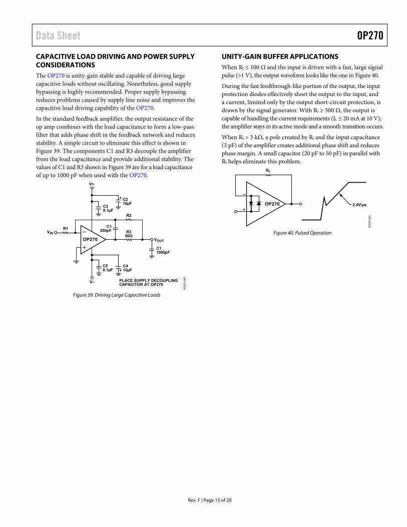
CAPACITIVE LOAD DRIVING AND POWER SUPPLY CONSIDERATIONS The OP270 is unity-gain stable and capable of driving large capacitive loads without oscillating. Nonetheless, good supply bypassing is highly recommended. Proper supply bypassing reduces problems caused by supply line noise and improves the capacitive load driving capability of the OP270.
In the standard feedback amplifier, the output resistance of the op amp combines with the load capacitance to form a low-pass filter that adds phase shift in the feedback network and reduces stability. A simple circuit to eliminate this effect is shown in Figure 39. The components C1 and R3 decouple the amplifier from the load capacitance and provide additional stability. The values of C1 and R3 shown in Figure 39 are for a load capacitance of up to 1000 pF when used with the OP270.
0032
5-04
0
C1200pFVIN
VOUT
PLACE SUPPLY DECOUPLINGCAPACITOR AT OP270
OP270
V+
R1
C30.1µF
C210µF
C11000pF
R2
C410µF
C50.1µF
R350Ω
+
V–
+
Figure 39. Driving Large Capacitive Loads
UNITY-GAIN BUFFER APPLICATIONS When Rf ≤ 100 Ω and the input is driven with a fast, large signal pulse (>1 V), the output waveform looks like the one in Figure 40.
During the fast feedthrough-like portion of the output, the input protection diodes effectively short the output to the input, and a current, limited only by the output short-circuit protection, is drawn by the signal generator. With Rf ≥ 500 Ω, the output is capable of handling the current requirements (IL ≤ 20 mA at 10 V); the amplifier stays in its active mode and a smooth transition occurs.
When Rf > 3 kΩ, a pole created by Rf and the input capacitance (3 pF) of the amplifier creates additional phase shift and reduces phase margin. A small capacitor (20 pF to 50 pF) in parallel with Rf helps eliminate this problem.
0032
5-04
1
OP270 2.4V/µs
Rf
Figure 40. Pulsed Operation
OP270 Data Sheet
Rev. F | Page 16 of 20
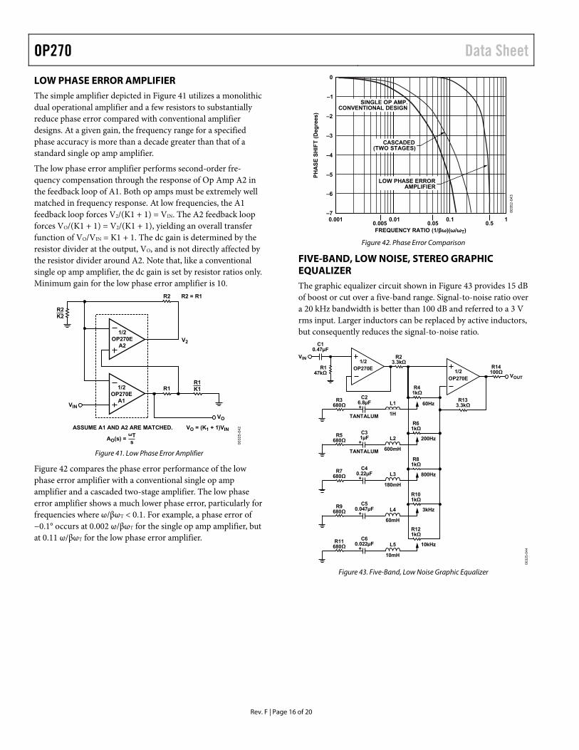
LOW PHASE ERROR AMPLIFIER The simple amplifier depicted in Figure 41 utilizes a monolithic dual operational amplifier and a few resistors to substantially reduce phase error compared with conventional amplifier designs. At a given gain, the frequency range for a specified phase accuracy is more than a decade greater than that of a standard single op amp amplifier.
The low phase error amplifier performs second-order fre- quency compensation through the response of Op Amp A2 in the feedback loop of A1. Both op amps must be extremely well matched in frequency response. At low frequencies, the A1 feedback loop forces V2/(K1 + 1) = VIN. The A2 feedback loop forces VO/(K1 + 1) = V2/(K1 + 1), yielding an overall transfer function of VO/VIN = K1 + 1. The dc gain is determined by the resistor divider at the output, VO, and is not directly affected by the resistor divider around A2. Note that, like a conventional single op amp amplifier, the dc gain is set by resistor ratios only. Minimum gain for the low phase error amplifier is 10.
0032
5-04
2
1/2OP270E
A2
1/2OP270E
A1
R1
VO
V2
VIN
R1K1
R2 R2 = R1
ωTs
R2K2
VO = (K1 + 1)VINASSUME A1 AND A2 ARE MATCHED.
AO(s) =
Figure 41. Low Phase Error Amplifier
Figure 42 compares the phase error performance of the low phase error amplifier with a conventional single op amp amplifier and a cascaded two-stage amplifier. The low phase error amplifier shows a much lower phase error, particularly for frequencies where ω/βωT < 0.1. For example, a phase error of −0.1° occurs at 0.002 ω/βωT for the single op amp amplifier, but at 0.11 ω/βωT for the low phase error amplifier.
0035
2-04
3
–7
–6
–5
–4
–3
–2
–1
0
PH
AS
E S
HIF
T (
Deg
rees
)
FREQUENCY RATIO (1/βω)(ω/ωT)
0.0010.005
0.01 0.1 1
LOW PHASE ERRORAMPLIFIER
CASCADED(TWO STAGES)
SINGLE OP AMP.CONVENTIONAL DESIGN
0.05 0.5
Figure 42. Phase Error Comparison
FIVE-BAND, LOW NOISE, STEREO GRAPHIC EQUALIZER The graphic equalizer circuit shown in Figure 43 provides 15 dB of boost or cut over a five-band range. Signal-to-noise ratio over a 20 kHz bandwidth is better than 100 dB and referred to a 3 V rms input. Larger inductors can be replaced by active inductors, but consequently reduces the signal-to-noise ratio.
0032
5-04
4
1/2OP270E
1/2OP270E
R23.3kΩ
R147kΩ
R41kΩ
60Hz
TANTALUM
VOUT
VIN
R14100Ω
R133.3kΩ
C26.8µF L1
1H
C10.47µF
R3680Ω
200Hz
R61kΩ
800Hz
R81kΩ
3kHz
R101kΩ
10kHz
R121kΩ
+
TANTALUM
C31µF L2
600mH
R5680Ω +
C40.22µF L3
180mH
R7680Ω +
C50.047µF L4
60mH
R9680Ω +
C60.022µF L5
10mH
R11680Ω +
Figure 43. Five-Band, Low Noise Graphic Equalizer

Data Sheet OP270
Rev. F | Page 17 of 20
DIGITAL PANNING CONTROL Figure 44 uses a DAC8221 (a dual 12-bit CMOS DAC) to pan a signal between two channels. One channel is formed by the current output of DAC A driving one-half of an OP270 in a current-to-voltage converter configuration. The other channel is formed by the complementary output current of DAC A, which normally flows to ground through the AGND pin. This complementary current is converted to a voltage by the other half of the OP270, which also holds AGND at virtual ground.
Gain error due to mismatching between the internal DAC ladder resistors and the current-to-voltage feedback resistors is eliminated by using feedback resistors internal to the DAC8221. Only DAC A passes a signal; DAC B provides the second feedback resistor. With VREFB unconnected, the current-to-voltage converter, using RFBB, is accurate and not influenced by digital data reaching DAC B. Distortion of the digital panning control is less than 0.002% over the 20 Hz to 20 kHz audio range. Figure 45 shows the complementary outputs for a 1 kHz input signal and a digital ramp applied to the DAC data input.
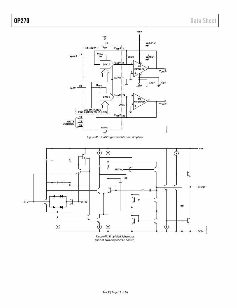
DUAL PROGRAMMABLE GAIN AMPLIFIER The dual OP270 and the DAC8221 (a dual 12-bit CMOS DAC) can be combined to form a space-saving, dual programmable amplifier. The digital code present at the DAC, which is easily set by a microprocessor, determines the ratio between the internal feedback resistor and the resistance that the DAC ladder presents to the op amp feedback loop. Gain of each amplifier is
nVV
IN
O 4096
where n is the decimal equivalent of the 12-bit digital code present at the DAC.
If the digital code present at the DAC consists of all 0s, the feedback loop opens, causing the op amp output to saturate. A 20 MΩ resistor placed in parallel with the DAC feedback loop eliminates this problem with only a very small reduction in gain accuracy.
0032
5-04
5
1/2OP270GP
VIN
NC
RFBA
1
1
23
2422
18
19CS
WRWRITE
CONTROL 20
6
5
7
3
24
3
21
VDD
DAC8221P
2 8
4
0.01µF
+15V
–15V
OUT
IOUTA
IOUTB
AGND
DGND5
1/2OP270GP
DAC B
DAC A
+5V
10µF–
+
10µF–+
0.1µF
RFBB
VREFA
VREFB
DAC A/DAC B
DAC DATA BUSPINS 6 (MSB) TO 17 (LSB)
OUT
Figure 44. Digital Panning Control
0035
2-04
6
5V5V 1ms
A OUT
A OUT
Figure 45. Digital Panning Control Output
OP270 Data Sheet
Rev. F | Page 18 of 20
0032
5-04
7
VINB
1
19
18
WRITECONTROL 20
6
5
7
3
23
21
VDDDAC8221P
2 8
4
DGND5
1/2OP270GP
1/2OP270EZ
DAC B
DAC A
+5V
0.01µF
+15V
10µF–+
–15V
10µF–+
0.1µF
24
22
1
IOUTB
2IOUTA
AGND
VREFB
4VREFA
VOUTB
VOUTA
20MΩ
20MΩ
DAC DATA BUSPINS 6 (MSB) TO 17 (LSB)
RFBB
VINA3 RFBA
Figure 46. Dual Programmable Gain Amplifier
BIAS
0032
5-00
3
V–
–IN
V+
OUT
+IN
Figure 47. Simplified Schematic
(One of Two Amplifiers Is Shown)
Data Sheet OP270
Rev. F | Page 19 of 20
OUTLINE DIMENSIONS
CONTROLLING DIMENSIONS ARE IN INCHES; MILLIMETER DIMENSIONS(IN PARENTHESES) ARE ROUNDED-OFF INCH EQUIVALENTS FORREFERENCE ONLY AND ARE NOT APPROPRIATE FOR USE IN DESIGN.
0.310 (7.87)0.220 (5.59)
0.005 (0.13)MIN
0.055 (1.40)MAX
0.100 (2.54) BSC
15° 0°
0.320 (8.13)0.290 (7.37)
0.015 (0.38)0.008 (0.20)
SEATINGPLANE
0.200 (5.08)MAX
0.405 (10.29) MAX
0.150 (3.81)MIN
0.200 (5.08)0.125 (3.18)
0.023 (0.58)0.014 (0.36) 0.070 (1.78)
0.030 (0.76)
0.060 (1.52)0.015 (0.38)
1 4
58
Figure 48. 8-Lead Ceramic Dual In-Line Package [CERDIP]
Z-Suffix (Q-8)
Dimensions shown in inches and (millimeters)
COMPLIANT TO JEDEC STANDARDS MS-001
CONTROLLING DIMENSIONS ARE IN INCHES; MILLIMETER DIMENSIONS(IN PARENTHESES) ARE ROUNDED-OFF INCH EQUIVALENTS FORREFERENCE ONLY AND ARE NOT APPROPRIATE FOR USE IN DESIGN.CORNER LEADS MAY BE CONFIGURED AS WHOLE OR HALF LEADS. 07
0606
-A
0.022 (0.56)0.018 (0.46)0.014 (0.36)
SEATINGPLANE
0.015(0.38)MIN
0.210 (5.33)MAX
0.150 (3.81)0.130 (3.30)0.115 (2.92)
0.070 (1.78)0.060 (1.52)0.045 (1.14)
8
1 4
5 0.280 (7.11)0.250 (6.35)0.240 (6.10)
0.100 (2.54)BSC
0.400 (10.16)0.365 (9.27)0.355 (9.02)
0.060 (1.52)MAX
0.430 (10.92)MAX
0.014 (0.36)0.010 (0.25)0.008 (0.20)
0.325 (8.26)0.310 (7.87)0.300 (7.62)
0.195 (4.95)0.130 (3.30)0.115 (2.92)
0.015 (0.38)GAUGEPLANE
0.005 (0.13)MIN
Figure 49. 8-Lead Plastic Dual In-Line Package [PDIP]
Narrow Body P-Suffix
(N-8) Dimensions shown in inches and (millimeters)
OP270 Data Sheet
Rev. F | Page 20 of 20
CONTROLLING DIMENSIONS ARE IN MILLIMETERS; INCH DIMENSIONS(IN PARENTHESES) ARE ROUNDED-OFF MILLIMETER EQUIVALENTS FORREFERENCE ONLY AND ARE NOT APPROPRIATE FOR USE IN DESIGN.
COMPLIANT TO JEDEC STANDARDS MS-013-AA
032
707-
B
10.50 (0.4134)10.10 (0.3976)
0.30 (0.0118)0.10 (0.0039)
2.65 (0.1043)2.35 (0.0925)
10.65 (0.4193)10.00 (0.3937)
7.60 (0.2992)7.40 (0.2913)
0.75 (0.0295)0.25 (0.0098)
45°
1.27 (0.0500)0.40 (0.0157)
COPLANARITY0.10 0.33 (0.0130)
0.20 (0.0079)
0.51 (0.0201)0.31 (0.0122)
SEATINGPLANE
8°0°
16 9
81
1.27 (0.0500)BSC
Figure 50. 16-Lead Standard Small Outline Package [SOIC_W]
Wide Body S-Suffix (RW-16)
Dimensions shown in millimeters and (inches)
ORDERING GUIDE
Model1 TA = +25°C VOS Max (μV)
θJC (°C/W)
θJA2
(°C/W) Temperature Range Package Description Package Option
OP270EZ 75 12 134 −40°C to +85°C 8-Lead CERDIP Q-8 (Z-Suffix) OP270FZ 150 12 134 −40°C to +85°C 8-Lead CERDIP Q-8 (Z-Suffix) OP270GP 250 37 96 −40°C to +85°C 8-Lead PDIP N-8 (P-Suffix) OP270GPZ −40°C to +85°C 8-Lead PDIP N-8 (P-Suffix) OP270GS 250 27 92 −40°C to +85°C 16-Lead SOIC_W RW-16 (S-Suffix) OP270GS-REEL −40°C to +85°C 16-Lead SOIC_W RW-16 (S-Suffix) OP270GSZ −40°C to +85°C 16-Lead SOIC_W RW-16 (S-Suffix) OP270GSZ-REEL −40°C to +85°C 16-Lead SOIC_W RW-16 (S-Suffix) 1 The OP270GPZ, OP270GSZ, and OP270GSZ-REEL are RoHS compliant parts. 2 θJA is specified for worst-case mounting conditions, that is, θJA is specified for device in socket for CERDIP and PDIP packages; θJA is specified for device soldered to
printed circuit board for SOIC package.
©2001–2015 Analog Devices, Inc. All rights reserved. Trademarks and registered trademarks are the property of their respective owners. D00325-0-10/15(F)