Dual, Low-Power, Single-Supply, Wideband … = +5V) ±5V or +10V supplies is also supported. The...
43
1FEATURES DESCRIPTION APPLICATIONS RELATED PRODUCTS Single-Supply, Differential, 2nd-Order, 5MHz, Low-Pass Sallen-Key Filter 1500Ω 506Ω 0.1μF 506Ω 238Ω 5kΩ 5kΩ 238Ω 0.1μF 750Ω 750Ω V O V I +5V 1/2 OPA2830 1/2 OPA2830 238Ω 238Ω BUF602 150pF 150pF 100pF 100pF 0.1μF +5V 2.5V OPA2830 www.ti.com.................................................................................................................................................. SBOS309D–AUGUST 2004–REVISED AUGUST 2008 Dual, Low-Power, Single-Supply, Wideband OPERATIONAL AMPLIFIER 2• HIGH BANDWIDTH: The OPA2830 is a dual, low-power, single-supply, 230MHz (G = +1), 100MHz (G = +2) wideband, voltage-feedback amplifier designed to operate on a single +3V or +5V supply. Operation on • LOW SUPPLY CURRENT: 7.8mA (V S = +5V) ±5V or +10V supplies is also supported. The input • FLEXIBLE SUPPLY RANGE: range extends below ground and to within 1.8V of the ±1.5V to ±5.5V Dual Supply positive supply. Using complementary +3V to +11V Single Supply common-emitter outputs provides an output swing to • INPUT RANGE INCLUDES GROUND ON within 25mV of ground and +V S while driving 150Ω. High output drive current (75mA) and low differential SINGLE SUPPLY gain and phase errors also make it ideal for • 4.82V PP OUTPUT SWING ON +5V SUPPLY single-supply consumer video products. • HIGH SLEW RATE: 500V/μs Low distortion operation is ensured by the high gain • LOW INPUT VOLTAGE NOISE: 9.2nV/√Hz bandwidth product (100MHz) and slew rate • AVAILABLE IN AN MSOP-8 PACKAGE (500V/μs), making the OPA2830 an ideal input buffer stage to 3V and 5V CMOS Analog-to-Digital Converters (ADCs). Unlike earlier low-power, single-supply amplifiers, distortion performance • SINGLE-SUPPLY ADC INPUT BUFFERS improves as the signal swing is decreased. A low • SINGLE-SUPPLY VIDEO LINE DRIVERS 9.2nV/√Hz input voltage noise supports wide dynamic • CCD IMAGING CHANNELS range operation. • LOW-POWER ULTRASOUND The OPA2830 is available in an industry-standard • PLL INTEGRATORS SO-8 package. The OPA2830 is also available in a • PORTABLE CONSUMER ELECTRONICS small MSOP-8 package. For fixed-gain and line driver • LOW-POWER ACTIVE FILTERS applications, consider the OPA2832. DESCRIPTION SINGLES DUALS TRIPLES QUADS Rail-to-Rail OPA830 — — OPA4830 Rail-to-Rail Fixed-Gain OPA832 OPA2832 OPA3832 — General-Purpose OPA690 OPA2690 OPA3690 — (1800V/s slew rate) Low-Noise, OPA820 OPA2822 — OPA4820 High DC Precision 1 Please be aware that an important notice concerning availability, standard warranty, and use in critical applications of Texas Instruments semiconductor products and disclaimers thereto appears at the end of this data sheet. 2All trademarks are the property of their respective owners. PRODUCTION DATA information is current as of publication date. Copyright © 2004–2008, Texas Instruments Incorporated Products conform to specifications per the terms of the Texas Instruments standard warranty. Production processing does not necessarily include testing of all parameters.
Transcript of Dual, Low-Power, Single-Supply, Wideband … = +5V) ±5V or +10V supplies is also supported. The...

1FEATURES DESCRIPTION
APPLICATIONS
RELATED PRODUCTS
Single-Supply , Differential, 2nd-Order , 5MHz, Low-Pass Sallen-Key Filter
1500Ω
506Ω0.1µF
506Ω
238Ω
5kΩ
5kΩ
238Ω0.1µF
750Ω
750Ω
VOVI
+5V
1/2OPA2830
1/2OPA2830
238Ω
238Ω
BUF602
150pF
150pF
100pF
100pF
0.1µF
+5V
2.5V
OPA2830
www.ti.com.................................................................................................................................................. SBOS309D–AUGUST 2004–REVISED AUGUST 2008
Dual, Low-Power, Single-Supply, WidebandOPERATIONAL AMPLIFIER
2• HIGH BANDWIDTH: The OPA2830 is a dual, low-power, single-supply,230MHz (G = +1), 100MHz (G = +2) wideband, voltage-feedback amplifier designed to
operate on a single +3V or +5V supply. Operation on• LOW SUPPLY CURRENT: 7.8mA (VS = +5V)±5V or +10V supplies is also supported. The input• FLEXIBLE SUPPLY RANGE: range extends below ground and to within 1.8V of the±1.5V to ±5.5V Dual Supply positive supply. Using complementary
+3V to +11V Single Supply common-emitter outputs provides an output swing to• INPUT RANGE INCLUDES GROUND ON within 25mV of ground and +VS while driving 150Ω.
High output drive current (75mA) and low differentialSINGLE SUPPLYgain and phase errors also make it ideal for• 4.82VPP OUTPUT SWING ON +5V SUPPLYsingle-supply consumer video products.
• HIGH SLEW RATE: 500V/µsLow distortion operation is ensured by the high gain• LOW INPUT VOLTAGE NOISE: 9.2nV/√Hz bandwidth product (100MHz) and slew rate
• AVAILABLE IN AN MSOP-8 PACKAGE (500V/µs), making the OPA2830 an ideal input bufferstage to 3V and 5V CMOS Analog-to-DigitalConverters (ADCs). Unlike earlier low-power,single-supply amplifiers, distortion performance• SINGLE-SUPPLY ADC INPUT BUFFERSimproves as the signal swing is decreased. A low• SINGLE-SUPPLY VIDEO LINE DRIVERS9.2nV/√Hz input voltage noise supports wide dynamic• CCD IMAGING CHANNELS range operation.
• LOW-POWER ULTRASOUNDThe OPA2830 is available in an industry-standard• PLL INTEGRATORS SO-8 package. The OPA2830 is also available in a
• PORTABLE CONSUMER ELECTRONICS small MSOP-8 package. For fixed-gain and line driver• LOW-POWER ACTIVE FILTERS applications, consider the OPA2832.
DESCRIPTION SINGLES DUALS TRIPLES QUADS
Rail-to-Rail OPA830 — — OPA4830
Rail-to-Rail Fixed-Gain OPA832 OPA2832 OPA3832 —
General-Purpose OPA690 OPA2690 OPA3690 —(1800V/s slew rate)
Low-Noise, OPA820 OPA2822 — OPA4820High DC Precision
1
Please be aware that an important notice concerning availability, standard warranty, and use in critical applications of TexasInstruments semiconductor products and disclaimers thereto appears at the end of this data sheet.
2All trademarks are the property of their respective owners.
PRODUCTION DATA information is current as of publication date. Copyright © 2004–2008, Texas Instruments IncorporatedProducts conform to specifications per the terms of the TexasInstruments standard warranty. Production processing does notnecessarily include testing of all parameters.

ABSOLUTE MAXIMUM RATINGS (1)
PIN CONFIGURATIONS
+VS
Output 2
−Input 2
+Input 2
Output 1
−Input 1
+Input 1
−VS
1
2
3
4
8
7
6
5
Top View SO, MSOP
OPA2830
SBOS309D–AUGUST 2004–REVISED AUGUST 2008.................................................................................................................................................. www.ti.com
This integrated circuit can be damaged by ESD. Texas Instruments recommends that all integrated circuits be handled withappropriate precautions. Failure to observe proper handling and installation procedures can cause damage.
ESD damage can range from subtle performance degradation to complete device failure. Precision integrated circuits may be moresusceptible to damage because very small parametric changes could cause the device not to meet its published specifications.
ORDERING INFORMATION (1)
SPECIFIEDPACKAGE TEMPERATURE PACKAGE ORDERING TRANSPORT
PRODUCT PACKAGE-LEAD DESIGNATOR RANGE MARKING NUMBER MEDIA, QUANTITYOPA2830ID Rails, 100
OPA2830 SO-8 Surface-Mount D –40°C to +85°C OPA2830OPA2830IDR Tape and Reel, 2500
OPA2830IDGKT Tape and Reel, 250OPA2830 MSOP-8 DGK –40°C to +85°C A59
OPA2830IDGKR Tape and Reel, 2500
(1) For the most current package and ordering information see the Package Option Addendum at the end of this document, or see the TIweb site at www.ti.com.
Power Supply 11VDC
Internal Power Dissipation See Thermal CharacteristicsDifferential Input Voltage ±2.5VInput Voltage Range –0.5V to +VS + 0.3VStorage Temperature Range: D, DGK –65°C to +125°CLead Temperature (soldering, 10s) +300°CJunction Temperature (TJ) +150°CESD Rating:
Human Body Model (HBM) 2000VCharge Device Model (CDM) 1000VMachine Model (MM) 200V
(1) Stresses above these ratings may cause permanent damage. Exposure to absolute maximum conditions for extended periods maydegrade device reliability. These are stress ratings only, and functional operation of the device at these or any other conditions beyondthose specified is not supported.
2 Submit Documentation Feedback Copyright © 2004–2008, Texas Instruments Incorporated
Product Folder Link(s): OPA2830

ELECTRICAL CHARACTERISTICS: VS = ±5V
OPA2830
www.ti.com.................................................................................................................................................. SBOS309D–AUGUST 2004–REVISED AUGUST 2008
Boldface limits are tested at +25C.At TA = +25°C, G = +2V/V, RF = 750Ω, and RL = 150Ω to GND, unless otherwise noted (see Figure 70).
OPA2830ID, IDGK
MIN/MAX OVERTYP TEMPERATURE
0°C to –40°C to MIN/ TESTPARAMETER CONDITIONS +25°C +25°C (1) +70°C (2) +85°C (2) UNITS MAX LEVEL (3)
AC PERFORMANCE (see Figure 70)
Small-Signal Bandwidth G = +1, VO ≤ 0.2VPP 290 MHz typ C
G = +2, VO ≤ 0.2VPP 105 66 64 61 MHz min B
G = +5, VO ≤ 0.2VPP 22 16 14 13 MHz min B
G = +10, VO ≤ 0.2VPP 10 8 7 6 MHz min B
Gain Bandwidth Product G ≥ +10 100 80 77 75 MHz min B
Peaking at a Gain of +1 VO ≤ 0.2VPP 4 dB typ C
Slew Rate G = +2, 2V Step 560 275 265 255 V/µs min B
Rise Time 0.5V Step 3.4 5.9 5.95 6.0 ns max B
Fall Time 0.5V Step 3.6 6.0 6.05 6.1 ns max B
Settling Time to 0.1% G = +2, 1V Step 43 64 66 67 ns max B
Harmonic Distortion VO = 2VPP, f = 5MHz
2nd-Harmonic RL = 150Ω –62 –55 –53 –52 dBc min B
RL ≥ 500Ω –66 –58 –57 –56 dBc min B
3rd-Harmonic RL = 150Ω –59 –50 –49 –48 dBc min B
RL ≥ 500Ω –77 –65 –62 –55 dBc min B
Input Voltage Noise f > 1MHz 9.5 10.6 11.1 11.6 nV/√Hz max B
Input Current Noise f > 1MHz 3.7 4.8 5.3 5.8 pA/√Hz max B
NTSC Differential Gain 0.07 % typ C
NTSC Differential Phase 0.17 ° typ C
DC PERFORMANCE (4) RL = 150Ω
Open-Loop Voltage Gain 74 66 65 64 dB min A
Input Offset Voltage ±1.5 ±7.5 ±8.7 ±9.3 mV max A
Average Offset Voltage Drift — ±27 ±27 µV/°C max B
Input Bias Current VCM = 2.0V +5 +10 +12 +13 µA max A
Input Bias Current Drift ±44 ±46 nA/°C max B
Input Offset Current VCM = 2.0V ±0.2 ±1.1 ±1.3 ±1.5 µA max A
Input Offset Current Drift — ±5 ±6 nA/°C max B
INPUT
Negative Input Voltage –5.5 –5.4 –5.3 –5.2 V max A
Positive Input Voltage 3.2 3.1 3.0 2.9 V min A
Common-Mode Rejection Ratio (CMRR) Input-Referred 80 76 74 71 dB min A
Input Impedance
Differential Mode 10 || 2.1 kΩ || pF typ C
Common-Mode 400 || 1.2 kΩ || pF typ C
OUTPUT
Output Voltage Swing G = +2, RL = 1kΩ to GND ±4.88 ±4.86 ±4.85 ±4.84 V min A
G = +2, RL = 150Ω to GND ±4.64 ±4.60 ±4.58 ±4.56 V min A
Current Output, Sinking and Sourcing ±82 ±63 ±58 ±53 mA min A
Short-Circuit Current Output Shorted to Ground 150 mA typ C
Closed-Loop Output Impedance G = +2, f ≤ 100kHz 0.06 Ω typ C
(1) Junction temperature = ambient for +25°C specifications.(2) Junction temperature = ambient at low temperature limits; junction temperature = ambient +18°C at high temperature limit for over
temperature specifications.(3) Test levels: (A) 100% tested at +25°C. Over temperature limits by characterization and simulation. (B) Limits set by characterization and
simulation. (C) Typical value only for information.(4) Current is considered positive out of pin.
Copyright © 2004–2008, Texas Instruments Incorporated Submit Documentation Feedback 3
Product Folder Link(s): OPA2830

OPA2830
SBOS309D–AUGUST 2004–REVISED AUGUST 2008.................................................................................................................................................. www.ti.com
ELECTRICAL CHARACTERISTICS: VS = ±5V (continued)Boldface limits are tested at +25C.At TA = +25°C, G = +2V/V, RF = 750Ω, and RL = 150Ω to GND, unless otherwise noted (see Figure 70).
OPA2830ID, IDGK
MIN/MAX OVERTYP TEMPERATURE
0°C to –40°C to MIN/ TESTPARAMETER CONDITIONS +25°C +25°C (1) +70°C (2) +85°C (2) UNITS MAX LEVEL (3)
POWER SUPPLY
Minimum Operating Voltage ±1.4 V typ C
Maximum Operating Voltage ±5.5 ±5.5 ±5.5 V max A
Maximum Quiescent Current VS = ±5V, Both Channels 8.5 9.5 10.7 11.9 mA max A
Minimum Quiescent Current VS = ±5V, Both Channels 8.5 8.0 7.2 6.6 mA min A
Power-Supply Rejection Ratio (–PSRR) Input-Referred 66 61 60 59 dB min A
THERMAL CHARACTERISTICS
Specification: ID, IDGK –40 to +85 °C typ C
Thermal Resistance, θJA
D SO-8 125 °C/W typ C
DGK MSOP-8 150 °C/W typ C
4 Submit Documentation Feedback Copyright © 2004–2008, Texas Instruments Incorporated
Product Folder Link(s): OPA2830

ELECTRICAL CHARACTERISTICS: VS = +5V
OPA2830
www.ti.com.................................................................................................................................................. SBOS309D–AUGUST 2004–REVISED AUGUST 2008
Boldface limits are tested at +25°C.At TA = +25°C, G = +2V/V, RF = 750Ω, and RL = 150Ω to VS/2, unless otherwise noted (see Figure 72).
OPA2830ID, IDGK
TYP MIN/MAX OVER TEMPERATURE
0°C to –40°C to MIN/ TESTPARAMETER CONDITIONS +25°C +25°C (1) +70°C (2) +85°C (2) UNITS MAX LEVEL (3)
AC PERFORMANCE (see Figure 72)
Small-Signal Bandwidth G = +1, VO ≤ 0.2VPP 230 MHz typ C
G = +2, VO ≤ 0.2VPP 100 70 68 66 MHz min B
G = +5, VO ≤ 0.2VPP 21 15 14 13 MHz min B
G = +10, VO ≤ 0.2VPP 10 7 6 5 MHz min B
Gain-Bandwidth Product G ≥ +10 100 75 65 59 MHz min B
Peaking at a Gain of +1 VO ≤ 0.2VPP 4 dB typ C
Slew Rate G = +2, 2V Step 500 270 260 250 V/µs min B
Rise Time 0.5V Step 3.4 5.8 5.9 6.0 ns max B
Fall Time 0.5V Step 3.4 5.8 5.9 6.0 ns max B
Settling Time to 0.1% G = +2, 1V Step 44 65 67 68 ns max B
Harmonic Distortion VO = 2VPP, f = 5MHz
2nd-Harmonic RL = 150Ω –58 –52 –51 –50 dBc min B
RL ≥ 500Ω –62 –56 –55 –54 dBc min B
3rd-Harmonic RL = 150Ω –58 –50 –49 –48 dBc min B
RL ≥ 500Ω –84 –65 –62 –60 dBc min B
Input Voltage Noise f > 1MHz 9.2 10.3 10.8 11.3 nV/√Hz max B
Input Current Noise f > 1MHz 3.5 4.6 5.1 5.6 pA/√Hz max B
NTSC Differential Gain 0.075 % typ C
NTSC Differential Phase 0.087 ° typ C
DC PERFORMANCE (4) RL = 150Ω
Open-Loop Voltage Gain 72 66 65 64 dB min A
Input Offset Voltage ±0.5 ±5.5 ±6.5 ±7.0 mV max A
Average Offset Voltage Drift — ±22 ±22 µV/°C max B
Input Bias Current VCM = 2.5V +5 +10 +12 +13 µA max A
Input Bias Current Drift ±44 ±46 nA/°C max B
Input Offset Current VCM = 2.5V ±0.2 ±0.9 ±1.1 ±1.3 µA max A
Input Offset Current Drift — ±5 ±6 nA/°C max B
INPUT
Least Positive Input Voltage –0.5 –0.4 –0.3 –0.2 V max A
Most Positive Input Voltage 3.2 3.1 3.0 2.9 V min A
Common-Mode Rejection Ratio (CMRR) Input-Referred 80 76 74 71 dB min A
Input Impedance, Differential Mode 10 || 2.1 kΩ || pF typ C
Common-Mode 400 || 1.2 kΩ || pF typ C
OUTPUT
Least Positive Output Voltage G = +5, RL = 1kΩ to 2.5V 0.09 0.11 0.12 0.13 V max A
G = +5, RL = 150Ω to 2.5V 0.21 0.24 0.25 0.26 V max A
Most Positive Output Voltage G = +5, RL = 1kΩ to 2.5V 4.91 4.89 4.88 4.87 V min A
G = +5, RL = 150Ω to 2.5V 4.78 4.75 4.73 4.72 V min A
Current Output, Sinking and Sourcing ±75 ±58 ±53 ±50 mA min A
Short-Circuit Output Current Output Shorted to Either Supply 140 mA typ C
Closed-Loop Output Impedance G = +2, f ≤ 100kHz 0.06 Ω typ C
(1) Junction temperature = ambient for +25°C specifications.(2) Junction temperature = ambient at low temperature limits; junction temperature = ambient +6°C at high temperature limit for over
temperature specifications.(3) Test levels: (A) 100% tested at +25°C. Over temperature limits by characterization and simulation. (B) Limits set by characterization and
simulation. (C) Typical value only for information.(4) Current is considered positive out of pin.
Copyright © 2004–2008, Texas Instruments Incorporated Submit Documentation Feedback 5
Product Folder Link(s): OPA2830

OPA2830
SBOS309D–AUGUST 2004–REVISED AUGUST 2008.................................................................................................................................................. www.ti.com
ELECTRICAL CHARACTERISTICS: VS = +5V (continued)Boldface limits are tested at +25°C.At TA = +25°C, G = +2V/V, RF = 750Ω, and RL = 150Ω to VS/2, unless otherwise noted (see Figure 72).
OPA2830ID, IDGK
TYP MIN/MAX OVER TEMPERATURE
0°C to –40°C to MIN/ TESTPARAMETER CONDITIONS +25°C +25°C (1) +70°C (2) +85°C (2) UNITS MAX LEVEL (3)
POWER SUPPLY
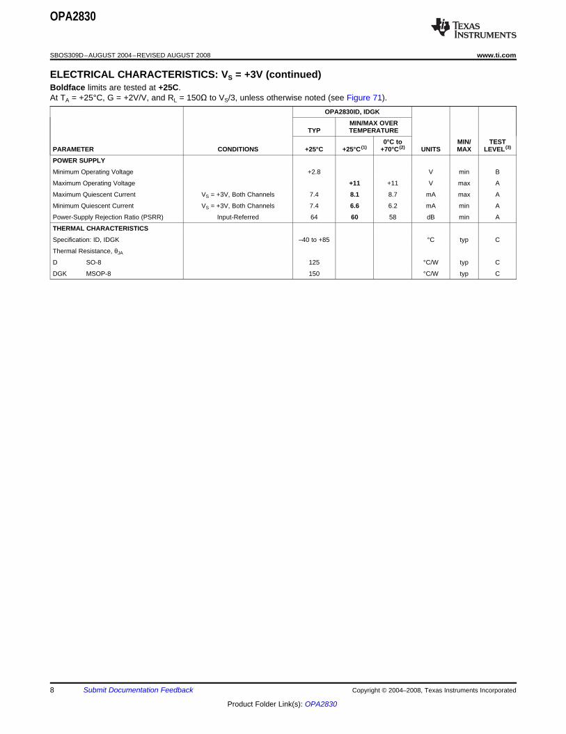
Minimum Operating Voltage +2.8 V min B
Maximum Operating Voltage +11 +11 +11 V max A
Maximum Quiescent Current VS = +5V, Both Channels 7.8 8.3 9.7 11.1 mA max A
Minimum Quiescent Current VS = +5V, Both Channels 7.8 7.4 6.8 6.2 mA min A
Power-Supply Rejection Ratio (PSRR) Input-Referred 66 61 60 59 dB min A
THERMAL CHARACTERISTICS
Specification: ID, IDGK –40 to +85 °C typ C
Thermal Resistance, θJA
D SO-8 125 °C/W typ C
DGK MSOP-8 150 °C/W typ C
6 Submit Documentation Feedback Copyright © 2004–2008, Texas Instruments Incorporated
Product Folder Link(s): OPA2830

ELECTRICAL CHARACTERISTICS: VS = +3V
OPA2830
www.ti.com.................................................................................................................................................. SBOS309D–AUGUST 2004–REVISED AUGUST 2008
Boldface limits are tested at +25C.At TA = +25°C, G = +2V/V, and RL = 150Ω to VS/3, unless otherwise noted (see Figure 71).
OPA2830ID, IDGK
MIN/MAX OVERTYP TEMPERATURE
0°C to MIN/ TESTPARAMETER CONDITIONS +25°C +25°C (1) +70°C (2) UNITS MAX LEVEL (3)
AC PERFORMANCE (see Figure 71)
Small-Signal Bandwidth G = +2, VO ≤ 0.2VPP 90 70 66 MHz min B
G = +5, VO ≤ 0.2VPP 20 15 14 MHz min B
G = +10, VO ≤ 0.2VPP 9 7.5 6.5 MHz min B
Gain-Bandwidth Product G ≥ +10 90 75 65 MHz min B
Slew Rate 1V Step 220 135 105 V/µs min B
Rise Time 0.5V Step 3.4 5.6 5.7 ns max B
Fall Time 0.5V Step 3.4 5.6 5.7 ns max B
Settling Time to 0.1% 1V Step 46 73 88 ns max B
Harmonic Distortion VO = 1VPP, f = 5MHz
2nd-Harmonic RL = 150Ω –60 –56 –54 dBc min B
RL ≥ 500Ω –64 –59 –57 dBc min B
3rd-Harmonic RL = 150Ω –68 –59 –58 dBc min B
RL ≥ 500Ω –72 –65 –64 dBc min B
Input Voltage Noise f > 1MHz 9.2 10.3 10.8 nV/√Hz max B
Input Current Noise f > 1MHz 3.5 4.6 5.1 pA/√Hz max B
DC PERFORMANCE (4)
Open-Loop Voltage Gain 72 66 65 dB min A
Input Offset Voltage ±1.5 ±7.5 ±8.7 mV max A
Average Offset Voltage Drift — ±27 µV/°C max B
Input Bias Current VCM = 1.0V +5 +10 +12 µA max A
Input Bias Current Drift ±44 nA/°C max B
Input Offset Current VCM = 1.0V ±0.2 ±1.1 ±1.3 µA max A
Input Offset Current Drift — ±5 nA/°C max B
INPUT
Least Positive Input Voltage –0.45 –0.4 –0.27 V max A
Most Positive Input Voltage 1.2 1.1 1.0 V min A
Common-Mode Rejection Ratio (CMRR) Input-Referred 80 74 72 dB min A
Input Impedance
Differential Mode 10 || 2.1 kΩ || pF typ C
Common-Mode 400 || 1.2 kΩ || pF typ C
OUTPUT
Least Positive Output Voltage G = +5, RL = 1kΩ to 1.5V 0.08 0.11 0.125 V max A
G = +5, RL = 150Ω to 1.5V 0.17 0.39 0.40 V max A
Most Positive Output Voltage G = +5, RL = 1kΩ to 1.5V 2.91 2.88 2.85 V min A
G = +5, RL = 150Ω to 1.5V 2.82 2.74 2.70 V min A
Current Output, Sinking and Sourcing ±30 ±20 ±18 mA min A
Short-Circuit Output Current Output Shorted to Either Supply 45 mA typ C
Closed-Loop Output Impedance See Figure 71, f < 100kHz 0.06 Ω typ C
(1) Junction temperature = ambient for +25°C specifications.(2) Junction temperature = ambient at low temperature limits; junction temperature = ambient +20°C at high temperature limit for over
temperature specifications.(3) Test levels: (A) 100% tested at +25°C. Over temperature limits by characterization and simulation. (B) Limits set by characterization and
simulation. (C) Typical value only for information.(4) Current is considered positive out of node.
Copyright © 2004–2008, Texas Instruments Incorporated Submit Documentation Feedback 7
Product Folder Link(s): OPA2830
OPA2830
SBOS309D–AUGUST 2004–REVISED AUGUST 2008.................................................................................................................................................. www.ti.com
ELECTRICAL CHARACTERISTICS: VS = +3V (continued)Boldface limits are tested at +25C.At TA = +25°C, G = +2V/V, and RL = 150Ω to VS/3, unless otherwise noted (see Figure 71).
OPA2830ID, IDGK
MIN/MAX OVERTYP TEMPERATURE
0°C to MIN/ TESTPARAMETER CONDITIONS +25°C +25°C (1) +70°C (2) UNITS MAX LEVEL (3)
POWER SUPPLY
Minimum Operating Voltage +2.8 V min B
Maximum Operating Voltage +11 +11 V max A
Maximum Quiescent Current VS = +3V, Both Channels 7.4 8.1 8.7 mA max A
Minimum Quiescent Current VS = +3V, Both Channels 7.4 6.6 6.2 mA min A
Power-Supply Rejection Ratio (PSRR) Input-Referred 64 60 58 dB min A
THERMAL CHARACTERISTICS
Specification: ID, IDGK –40 to +85 °C typ C
Thermal Resistance, θJA
D SO-8 125 °C/W typ C
DGK MSOP-8 150 °C/W typ C
8 Submit Documentation Feedback Copyright © 2004–2008, Texas Instruments Incorporated
Product Folder Link(s): OPA2830

TYPICAL CHARACTERISTICS: VS = ±5V
6
3
0
−3
−6
−9
−12
−15
−18
Frequency (MHz)
Nor
mal
ized
Ga
in(d
B)
1 10 100 600
VO = 0.2VPPRL = 150ΩSee Figure 72
G = +1RF = 0Ω
G = +2
G = +5
G = +10
3
0
−3
−6
−9
−12
−15
−18
Frequency (MHz)
Nor
mal
ized
Ga
in(d
B)
1 10 100 400
VO = 0.2VPPRL = 150Ω
G = −2
G = −10
G = −1
G = −5
3
0
−3
−6
−9
−12
−15
−18
Frequency (MHz)
Ga
in(d
B)
10 100 400
G = −1V/VRL = 150Ω
VO = 2VPP
VO = 4VPP
VO = 1VPP
VO = 0.5VPP
9
6
3
0
−3
−6
−9
−12
Frequency (MHz)
Gai
n(d
B)
10 100 400
VO = 4VPP
VO = 2VPP
VO = 1VPP
VO = 0.5VPP
G = +2V/VRL = 150ΩSee Figure 72
0.4
0.3
0.2
0.1
0
−0.1
−0.2
−0.3
−0.4Time (10ns/div)
Sm
all−
Sig
nalO
utp
utV
olta
ge
(V)
2.0
1.5
1.0
0.5
0
−0.5
−1.0
−1.5
−2.0
Lar
ge−
Sig
nalO
utp
utV
olta
ge(V
)
Large−Signal ± 1VRight Scale
Small−Signal ± 100mVLeft Scale
G = −1V/V0.4
0.3
0.2
0.1
0
−0.1
−0.2
−0.3
−0.4Time (10ns/div)
Sm
all−
Sig
nalO
utp
utV
olta
ge
(V)
2.0
1.5
1.0
0.5
0
−0.5
−1.0
−1.5
−2.0
Lar
ge−
Sig
nalO
utp
utV
olta
ge(V
)Large−Signal ± 1VRight Scale
Small−Signal ± 100mVLeft Scale
G = +2V/VSee Figure 72
OPA2830
www.ti.com.................................................................................................................................................. SBOS309D–AUGUST 2004–REVISED AUGUST 2008
At TA = +25°C, G = +2V/V, RF = 750Ω, and RL = 150Ω to GND, unless otherwise noted (see Figure 72).
NONINVERTING SMALL-SIGNAL FREQUENCY RESPONSE INVERTING SMALL-SIGNAL FREQUENCY RESPONSE
Figure 1. Figure 2.
NONINVERTING LARGE-SIGNALFREQUENCY RESPONSE INVERTING LARGE-SIGNAL FREQUENCY RESPONSE
Figure 3. Figure 4.
NONINVERTING PULSE RESPONSE INVERTING PULSE RESPONSE
Figure 5. Figure 6.
Copyright © 2004–2008, Texas Instruments Incorporated Submit Documentation Feedback 9
Product Folder Link(s): OPA2830

−50
−55
−60
−65
−70
−75
−80
−85
Resistance (Ω)
Har
mon
icD
isto
rtio
n(d
Bc)
100 1k
G = +2V/VVO = 2VPPf = 5MHzSee Figure 72
3rd−Harmonic
2nd−Harmonic
−40
−45
−50
−55
−60
−65
−70
−75
−80
−85
−90
Supply Voltage (±VS)
Har
mon
icD
isto
rtio
n(d
Bc)
2.0 2.5 3.0 3.5 4.0 4.5 5.0 6.05.5
G = +2V/VVO = 2VPPRL = 500Ω
See Figure 72
2nd−Harmonic
3rd−Harmonic
Input Limited for VCM = 0V
−55
−60
−65
−70
−75
−80
−85
−90
−95
Output Voltage Swing (VPP)
Ha
rmon
icD
isto
rtio
n(d
Bc)
0.1 1 10
2nd−Harmonic
3rd−Harmonic
G = +2V/VRL = 500Ωf = 5MHzSee Figure 72
−50
−55
−60
−65
−70
−75
−80
−85
−90
−95
−100
−105
Frequency (MHz)
Har
mon
icD
isto
rtio
n(d
Bc)
0.1 1 10
3rd−HarmonicRL = 150Ω
2nd−HarmonicRL = 150Ω
2nd−HarmonicRL = 500Ω
3rd−HarmonicRL = 500Ω
G = +2V/VVO = 2VPPSee Figure 72
−40
−45
−50
−55
−60
−65
−70
−75
−80
−85
−90
Single−Tone Load Power (2dBm/div)
3rd−
Ord
erS
pur
ious
Leve
l(dB
c)
−26 −20 −14 −8 −2 6
10MHz
5MHz
20MHz
750Ω
1 /2
OPA 28 30
PI
PO50Ω500Ω
750Ω
83
82
81
80
79
78
77
Ambient Temperature (C)
Out
put
Cur
rent
(mA
)
13
12
11
10
9
8
7
Sup
ply
Cur
ren
t(m
A)
−50 −25 0 25 50 75 100 125
Output Current (sourcing)
Output Current (sinking)
Quiescent Current (total, both amplifiers)
OPA2830
SBOS309D–AUGUST 2004–REVISED AUGUST 2008.................................................................................................................................................. www.ti.com
TYPICAL CHARACTERISTICS: VS = ±5V (continued)At TA = +25°C, G = +2V/V, RF = 750Ω, and RL = 150Ω to GND, unless otherwise noted (see Figure 72).
HARMONIC DISTORTION vs LOAD RESISTANCE 5MHz HARMONIC DISTORTION vs SUPPLY VOLTAGE
Figure 7. Figure 8.
HARMONIC DISTORTION vs OUTPUT VOLTAGE HARMONIC DISTORTION vs FREQUENCY
Figure 9. Figure 10.
TWO-TONE, 3RD-ORDER INTERMODULATION SPURIOUS SUPPLY AND OUTPUT CURRENT vs TEMPERATURE
Figure 11. Figure 12.
10 Submit Documentation Feedback Copyright © 2004–2008, Texas Instruments Incorporated
Product Folder Link(s): OPA2830

120
110
100
90
80
70
60
50
40
30
20
10
Capacitive Load (pF)
RS
(Ω)
1 10 100 1k
0dB Peaking Targeted8
7
6
5
4
3
2
1
0
−1
−2
−3
Frequency (MHz)
Nor
mal
ize
dG
ain
toC
apa
citiv
eLo
ad
(dB
)
1 10 100 200
CL = 1000pF
CL = 100pF
CL = 10pF
750Ω
RS1/2
OPA2830
VI
VO50Ω1kΩ(1)CL
750Ω NOTE: (1) 1kΩ is optional.
6
5
4
3
2
1
0
−1
−2
−3
−4
−5
−6
Resistance (Ω )
Out
put
Vol
tage
(V)
10 100 1k
G = +5V/VVS = ±5V
6
5
4
3
2
1
0
−1
−2
−3
−4
−5
−6
IO (mA)
VO
(V)
−160 −120 −80 −40 0 40 80 120 160
1W Internal
Power Lim it
Output
Current Limit
One Channel Only
Output
Current Lim it
1W Internal
Power Limit
RL = 500Ω
RL = 100ΩRL = 50Ω
OPA2830
www.ti.com.................................................................................................................................................. SBOS309D–AUGUST 2004–REVISED AUGUST 2008
TYPICAL CHARACTERISTICS: VS = ±5V (continued)At TA = +25°C, G = +2V/V, RF = 750Ω, and RL = 150Ω to GND, unless otherwise noted (see Figure 72).
FREQUENCY RESPONSE vs CAPACITIVE LOAD RECOMMENDED RS vs CAPACITIVE LOAD
Figure 13. Figure 14.
OUTPUT SWING vs LOAD RESISTANCE OUTPUT VOLTAGE AND CURRENT LIMITATIONS
Figure 15. Figure 16.
Copyright © 2004–2008, Texas Instruments Incorporated Submit Documentation Feedback 11
Product Folder Link(s): OPA2830

TYPICAL CHARACTERISTICS: VS = ±5V, Differential Configuration
3
0
−3
−6
−9
−12
−15
Frequency (MHz)
1 10 100 200
Nor
mal
ized
Gai
n(d
B)
GD = 1
GD = 2
GD = 5
GD = 10
VO = 200mVPPRL = 500Ω
RL500Ω
604Ω
604Ω
20Ω
20Ω
RG
RG
VOVI
GD = 604ΩRG
+5V
−5V
1/2OPA2830
1/2OPA2830
−45
−50
−55
−60
−65
−70
−75
−80
−85
−90
−95
−100
Resistance (Ω)
100 150 200 250 300 350 400 450 500
Ha
rmon
icD
isto
rtio
n(d
Bc) 3rd−Harmonic
2nd−Harmonic
GD = 2VO = 4VPPf = 5MHz
9
6
3
0
−3
−6
−9
Frequency (MHz)
1 10 200100
Gai
n(d
B)
VO = 5VPP
VO = 2VPP
VO = 1VPP
VO = 200mVPPGD = 2RL = 500Ω
−40
−50
−60
−70
−80
−90
−100
−110
Frequency (MHz)
0.1 1 10 100
Har
mon
icD
isto
rtio
n(d
Bc)
3rd−Harmonic
2nd−Harmonic
GD = 2VO = 4VPPRL = 500Ω
−55
−60
−65
−70
−75
−80
−85
−90
−95
−100
−105
Output Voltage Swing (VPP)
1 10
Har
mon
icD
istr
tion
(dB
c) 3rd−Harmonic
2nd−Harmonic
GD = 2RL = 500Ωf = 5MHz
OPA2830
SBOS309D–AUGUST 2004–REVISED AUGUST 2008.................................................................................................................................................. www.ti.com
At TA = +25°C, RF = 604Ω (as shown in Figure 17), and RL = 500Ω, unless otherwise noted.
DIFFERENTIAL SMALL-SIGNAL FREQUENCY RESPONSE
Figure 17. Figure 18.
DIFFERENTIAL LARGE-SIGNAL FREQUENCY RESPONSE DIFFERENTIAL DISTORTION vs LOAD RESISTANCE
Figure 19. Figure 20.
DIFFERENTIAL DISTORTION vs FREQUENCY DIFFERENTIAL DISTORTION vs OUTPUT VOLTAGE
Figure 21. Figure 22.
12 Submit Documentation Feedback Copyright © 2004–2008, Texas Instruments Incorporated
Product Folder Link(s): OPA2830

TYPICAL CHARACTERISTICS: VS = +5V
6
3
0
−3
−6
−9
−12
−15
−18
Frequency (MHz)
Nor
mal
ized
Ga
in(d
B)
1 10 100 500
VO = 0.2VPPRL = 150ΩSee Figure 70
G = +1RF = 0Ω
G = +2
G = +5
G = +10
3
0
−3
−6
−9
−12
−15
−18
Frequency (MHz)
Nor
mal
ized
Ga
in(d
B)
1 10 100 300
VO = 0.2VPPRL = 150ΩSee Figure 84
G = −2
G = −10
G = −1
G = −5
9
6
3
0
−3
−6
−9
−12
Frequency (MHz)
Ga
in(d
B)
10 100 400
G = +2V/VRL = 150ΩSee Figure 70
VO = 2VPP
VO = 1VPPVO = 0.5VPP
3
0
−3
−6
−9
−12
−15
−18
Frequency (MHz)
Ga
in(d
B)
10 100 300
G = −1V/VRL = 150ΩSee Figure 84
VO = 2VPPVO = 1VPP
VO = 0.5VPP
2.9
2.8
2.7
2.6
2.5
2.4
2.3
2.2
2.1Time (10ns/div)
Sm
all−
Sig
nalO
utp
utV
olta
ge
(V)
4.5
4.0
3.5
3.0
2.5
2.0
1.5
1.0
0.5
Lar
ge−
Sig
nalO
utp
utV
olta
ge(V
)
Large−Signal 1.5V to 3.5VRight Scale
Small−Signal 2.4V to 2.6VLeft Scale
G = −1V/V2.9
2.8
2.7
2.6
2.5
2.4
2.3
2.2
2.1Time (10ns/div)
Sm
all−
Sig
nalO
utp
utV
olta
ge
(V)
4.5
4.0
3.5
3.0
2.5
2.0
1.5
1.0
0.5
Lar
ge−
Sig
nalO
utp
utV
olta
ge(V
)Large−Signal 1.5V to 3.5VRight Scale
Small−Signal 2.4V to 2.6VLeft Scale
G = +2V/VSee Figure 70
OPA2830
www.ti.com.................................................................................................................................................. SBOS309D–AUGUST 2004–REVISED AUGUST 2008
At TA = +25°C, G = +2V/V, RF = 750Ω, RL = 150Ω to VS/2, and input VCM = 2.5V, unless otherwise noted (see Figure 70).
NONINVERTING SMALL-SIGNAL FREQUENCY RESPONSE INVERTING SMALL-SIGNAL FREQUENCY RESPONSE
Figure 23. Figure 24.
NONINVERTING LARGE-SIGNALFREQUENCY RESPONSE INVERTING LARGE-SIGNAL FREQUENCY RESPONSE
Figure 25. Figure 26.
NONINVERTING PULSE RESPONSE INVERTING PULSE RESPONSE
Figure 27. Figure 28.
Copyright © 2004–2008, Texas Instruments Incorporated Submit Documentation Feedback 13
Product Folder Link(s): OPA2830

−50
−55
−60
−65
−70
−75
−80
−85
−90
Load Resistance (Ω )
Har
mon
icD
isto
rtio
n(d
Bc)
100 1k
G = +2V/VVO = 2VPPf = 5MHzSee Figure 70
3rd−Harmonic
2nd−Harmonic
−45
−50
−55
−60
−65
−70
−75
−80
−85
−90
−95
−100
Frequency (MHz)
Har
mon
icD
isto
rtio
n(d
Bc)
0.1 1 10
3rd−HarmonicRL = 150Ω
2nd−HarmonicRL = 150Ω
2nd−HarmonicRL = 500Ω
3rd−HarmonicRL = 500Ω
G = +2V/VVO = 2VPPSee Figure 70
−55
−60
−65
−70
−75
−80
−85
−90
Gain (V/V)
Har
mon
icD
isto
rtio
n(d
Bc)
1 10
RL = 500ΩVO = 2VPPf = 5MHz
See Figure 70
3rd−Harmonic
2nd−Harmonic
−45
−50
−55
−60
−65
−70
−75
−80
−85
−90
−95
−100
Output Voltage Swing (VPP)
Ha
rmon
icD
isto
rtio
n(d
Bc)
0.1 1 10
2nd−Harmonic
3rd−Harmonic
G = +2V/VRL = 500Ωf = 5MHzSee Figure 70
Input Limited
−55
−60
−65
−70
−75
−80
−85
Gain ( V/V )
Ha
rmon
icD
isto
rtio
n(d
Bc)
1 10
RL = 500ΩVO = 2VPPf = 5MHz
3rd−Harmonic
2nd−Harmonic
−45
−50
−55
−60
−65
−70
−75
−80
−85
−90
−95
Single−Tone Load Power (dBm)
3rd−
Ord
erS
pur
ious
Leve
l(d
Bc)
10MHz
5MHz
20MHz
750Ω
1 /2
OP A28 30
PI
PO50Ω
500Ω
750Ω
−26 −24 −22 −20 −18 −16 −14 −12 −10 −8 −6 −4 −2
OPA2830
SBOS309D–AUGUST 2004–REVISED AUGUST 2008.................................................................................................................................................. www.ti.com
TYPICAL CHARACTERISTICS: VS = +5V (continued)At TA = +25°C, G = +2V/V, RF = 750Ω, RL = 150Ω to VS/2, and input VCM = 2.5V, unless otherwise noted (see Figure 70).
HARMONIC DISTORTION vs LOAD RESISTANCE HARMONIC DISTORTION vs FREQUENCY
Figure 29. Figure 30.
HARMONIC DISTORTION vs OUTPUT VOLTAGE HARMONIC DISTORTION vs NONINVERTING GAIN
Figure 31. Figure 32.
HARMONIC DISTORTION vs INVERTING GAIN TWO-TONE, 3RD-ORDER INTERMODULATION SPURIOUS
Figure 33. Figure 34.
14 Submit Documentation Feedback Copyright © 2004–2008, Texas Instruments Incorporated
Product Folder Link(s): OPA2830

100
10
1
0.1
0.01
Frequency (Hz)
1k 10k 100k 1M 10M 100M
Out
putI
mp
edan
ce( Ω
)
100
10
1
Frequency (Hz)
10 100 1k 10k 100k 1M 10M
Vo
ltage
No
ise
(nV
/√H
z)C
urre
ntN
ois
e(p
A/√
Hz)
Voltage Noise(9.2nV/√Hz)
Current Noise(3.5pA/√Hz)
130
120
110
100
90
80
70
60
50
40
30
20
10
Capacitive Load (pF)
RS
(Ω)
1 10 100 1k
< 0.5dB Peaking Targeted8
7
6
5
4
3
2
1
0
−1
−2
−3
Frequency (MHz)
Nor
mal
ize
dG
ain
toC
apa
citiv
eLo
ad
(dB
)
1 10 100 300
CL = 1000pF
CL = 100pF
CL = 10pF
750Ω
RS1/2OPA2830
VIVO50Ω
1kΩ(1)CL
750Ω NOTE: (1) 1kΩ is optional.
80
70
60
50
40
30
20
10
0
−10
−20
Frequency (Hz)
Op
en−
Loo
pG
ain
(dB
)
180
160
140
120
100
80
60
40
20
0
−20
Ope
n−Lo
opP
hase
(dB
)
100 1k 10k 100k 1M 10M 100M 1G
20 log (AOL)
∠ (AOL)
5.0
4.5
4.0
3.5
3.0
2.5
2.0
1.5
1.0
0.5
0
−0.5
−1.0
Ambient Temperature (10C/div)
−50 0 50 110
Vo
ltag
eR
ang
e(V
)
Most Positive Output Voltage
Most Positive Input Voltage
Least Positive Output Voltage
Least Positive Input Voltage
RL = 150Ω
OPA2830
www.ti.com.................................................................................................................................................. SBOS309D–AUGUST 2004–REVISED AUGUST 2008
TYPICAL CHARACTERISTICS: VS = +5V (continued)At TA = +25°C, G = +2V/V, RF = 750Ω, RL = 150Ω to VS/2, and input VCM = 2.5V, unless otherwise noted (see Figure 70).
INPUT VOLTAGE AND CURRENT NOISE DENSITY CLOSED-LOOP OUTPUT IMPEDANCE vs FREQUENCY
Figure 35. Figure 36.
RECOMMENDED RS vs CAPACITIVE LOAD FREQUENCY RESPONSE vs CAPACITIVE LOAD
Figure 37. Figure 38.
OPEN-LOOP GAIN AND PHASE VOLTAGE RANGES vs TEMPERATURE
Figure 39. Figure 40.
Copyright © 2004–2008, Texas Instruments Incorporated Submit Documentation Feedback 15
Product Folder Link(s): OPA2830

4
3
2
1
0
−1
−2
−3
−4
Ambient Temperature (C)
Inp
utO
ffset
Vol
tage
(mV
)
8
6
4
2
0
−2
−4
−6
−8
Inpu
tBia
san
dO
ffset
Cu
rren
t(µ A
)
−50 −25 0 25 50 75 100 125
Input Bias Current (IB)
10 × Input Offset Current (IOS)
Input Offset Voltage (VOS)
100
95
90
85
80
75
70
65
60
Ambient Temperature (C)
Out
putC
urr
ent(
mA
)
10.5
10.0
9.5
9.0
8.5
8.0
7.5
7.0
6.5
Su
pply
Cu
rre
nt(m
A)
−50 −25 0 25 50 75 100 125
Output Current, Sinking
Quiescent Current
Output Current, Sourcing
90
80
70
60
50
40
30
20
10
0
Frequency (Hz)
Com
mon
−M
ode
Re
ject
ion
Rat
io(d
B)
Pow
er−
Su
pply
Re
ject
ion
Ra
tio(d
B)
1k 10k 100k 1M 10M 100M
CMRR
PSRR
5.5
5.0
4.5
4.0
3.5
3.0
2.5
2.0
1.5
1.0
0.5
0
−0.5
Load Resistance (Ω )
Out
put
Vol
tage
(V)
10 100 1k
G = +5V/V
OPA2830
SBOS309D–AUGUST 2004–REVISED AUGUST 2008.................................................................................................................................................. www.ti.com
TYPICAL CHARACTERISTICS: VS = +5V (continued)At TA = +25°C, G = +2V/V, RF = 750Ω, RL = 150Ω to VS/2, and input VCM = 2.5V, unless otherwise noted (see Figure 70).
TYPICAL DC DRIFT OVER TEMPERATURE SUPPLY AND OUTPUT CURRENT vs TEMPERATURE
Figure 41. Figure 42.
CMRR AND PSRR vs FREQUENCY OUTPUT SWING vs LOAD RESISTANCE
Figure 43. Figure 44.
16 Submit Documentation Feedback Copyright © 2004–2008, Texas Instruments Incorporated
Product Folder Link(s): OPA2830

TYPICAL CHARACTERISTICS: VS = +5V, Differential Configuration
3
0
−3
−6
−9
−12
−15
Frequency (MHz)
1 10 100 200
Nor
mal
ized
Gai
n(d
B)
GD = 1
GD = 2
GD = 5
GD = 10
VO = 200mVPPRL = 500Ω
RL
604Ω
604ΩRG
VOVI
GD = 604ΩRG
+5V
1.2kΩ
1.2kΩ 0.1µF1/2
OPA2830
1/2OPA2830
RG
2.5V
2.5V
−40
−45
−50
−55
−60
−65
−70
−75
−80
−85
−90
Resistance (Ω )
100 150 200 250 300 350 400 450 500
Ha
rmon
icD
isto
rtio
n(d
Bc) 3rd−Harmonic
2nd−Harmonic
GD = 2VO = 4VPPf = 5MHz
9
6
3
0
−3
−6
−9
Frequency (MHz)
1 10 100 200
Gai
n(d
B)
VO = 3VPP
VO = 2VPP
VO = 1VPP
VO = 0.2VPPGD = 2RL = 500Ω
−30
−40
−50
−60
−70
−80
−90
−100
−110
Frequency (MHz)
1 10 100
Har
mon
icD
istr
tion
(dB
c)
3rd−Harmonic
2nd−Harmonic
GD = 2VO = 4VPPRL = 500Ω
−55
−60
−65
−70
−75
−80
−85
−90
−95
−100
Output Voltage Swing (VPP)
1 10
Har
mon
icD
istr
tion
(dB
c)
3rd−Harmonic
2nd−Harmonic
GD = 2RL = 500Ωf = 5MHz
OPA2830
www.ti.com.................................................................................................................................................. SBOS309D–AUGUST 2004–REVISED AUGUST 2008
At TA = +25°C, RF = 604Ω, and RL = 500Ω differential (as shown in Figure 45), unless otherwise noted.
DIFFERENTIAL SMALL-SIGNAL FREQUENCY RESPONSE
Figure 45. Figure 46.
DIFFERENTIAL LARGE-SIGNAL FREQUENCY RESPONSE DIFFERENTIAL DISTORTION vs LOAD RESISTANCE
Figure 47. Figure 48.
DIFFERENTIAL DISTORTION vs FREQUENCY DIFFERENTIAL DISTORTION vs OUTPUT VOLTAGE
Figure 49. Figure 50.
Copyright © 2004–2008, Texas Instruments Incorporated Submit Documentation Feedback 17
Product Folder Link(s): OPA2830

TYPICAL CHARACTERISTICS: VS = +3V
6
3
0
−3
−6
−9
−12
−15
−18
Frequency (MHz)
Nor
mal
ized
Ga
in(d
B)
1 10 100 400
RL = 150ΩVO = 0.2VPPSee Figure 71
G = +2
G = +10
G = +5
G = +1RF = 0
3
0
−3
−6
−9
−12
−15
−18
Frequency (MHz)
Nor
mal
ized
Ga
in(d
B)
1 10 100 300
G = −10
G = −5
G = −2
G = −1
RL = 150ΩVO = 0.2VPP
9
6
3
0
−3
−6
−9
−12
Frequency (MHz)
Ga
in(d
B)
10 100 300
G = +2V/VRL = 150ΩSee Figure 71
VO = 1.5VPP
VO = 1VPPVO = 0.5VPP
3
0
−3
−6
−9
−12
−15
−18
Frequency (MHz)
Ga
in(d
B)
10 100 300
G = −1V/VRL = 150Ω
VO = 1.5VPP
VO = 1VPP
VO = 0.5VPP
1.20
1.15
1.10
1.05
1.00
0.95
0.90
0.85
0.80Time (10ns/div)
Sm
all−
Sig
nalO
utp
utV
olta
ge
(V)
2.00
1.75
1.50
1.25
1.00
0.75
0.50
0.25
0
Lar
ge−
Sig
nalO
utp
utV
olta
ge(V
)
Large−Signal 0.5V to 1.5VRight Scale
Small−Signal 0.95V to 1.05VLeft Scale
G = −1V/VRL = 150Ω
1.20
1.15
1.10
1.05
1.00
0.95
0.90
0.85
0.80Time (10ns/div)
Sm
all−
Sig
nalO
utp
utV
olta
ge
(V)
2.00
1.75
1.50
1.25
1.00
0.75
0.50
0.25
0
Lar
ge−
Sig
nalO
utp
utV
olta
ge(V
)Large−Signal 0.5V to 1.5VRight Scale
Small−Signal0.95V to 1.05V
Left Scale
G = +2V/VSee Figure 71
OPA2830
SBOS309D–AUGUST 2004–REVISED AUGUST 2008.................................................................................................................................................. www.ti.com
At TA = +25°C, G = +2V/V, and RL = 150Ω to VS/3, unless otherwise noted (see Figure 71).
NONINVERTING SMALL-SIGNAL FREQUENCY RESPONSE INVERTING SMALL-SIGNAL FREQUENCY RESPONSE
Figure 51. Figure 52.
NONINVERTING LARGE-SIGNALFREQUENCY RESPONSE INVERTING LARGE-SIGNAL FREQUENCY RESPONSE
Figure 53. Figure 54.
NONINVERTING PULSE RESPONSE INVERTING PULSE RESPONSE
Figure 55. Figure 56.
18 Submit Documentation Feedback Copyright © 2004–2008, Texas Instruments Incorporated
Product Folder Link(s): OPA2830

−50
−55
−60
−65
−70
−75
−80
−85
−90
Resistance (Ω)
Har
mon
icD
isto
rtio
n(d
Bc)
100 1k
G = +2V/VVO = 1VPPf = 5MHz
See Figure 71
3rd−Harmonic
2nd−Harmonic
−30
−40
−50
−60
−70
−80
−90
Output Voltage Swing (VPP)
Ha
rmon
icD
isto
rtio
n(d
Bc)
0.1 1 10
2nd−Harmonic
3rd−Harmonic
G = +2V/VRL = 500Ωf = 5MHzSee Figure 71 Input Limited
−55
−60
−65
−70
−75
−80
−85
−90
−95
−100
Frequency (MHz)
Har
mon
icD
isto
rtio
n(d
Bc)
0.1 1 10
2nd−HarmonicRL = 150Ω
2nd−HarmonicRL = 500Ω
3rd−HarmonicRL = 150Ω
3rd−HarmonicRL = 500Ω
G = +2V/VVO = 1VPPSee Figure 71
−40
−45
−50
−55
−60
−65
−70
−75
−80
−85
−90
−95
Single−Tone Load Power (dBm)
3rd−
Ord
erS
pur
ious
Leve
l(d
Bc)
10MHz
5MHz
20MHz
−28 −26 −24 −22 −20 −18 −16 −14 −12 −10 −8
750Ω
1/2
O PA 2830
PIPO50Ω
500Ω
750Ω
190
170
150
130
110
90
70
50
30
10
Capacitive Load (pF)
RS
(Ω)
1 10 100 1k
< 0.5dB Peaking Targeted8
7
6
5
4
3
2
1
0
−1
−2
−3
Frequency (MHz)
No
rma
lized
Gai
nto
Cap
aci
tive
Loa
d(d
B)
1 10 100 200
CL = 1000pF
CL = 100pF
CL = 10pF
750Ω
RSVIVO50Ω
1kΩ(1)CL
750Ω NOTE: (1) 1kΩ is optional.
OPA2830
OPA2830
www.ti.com.................................................................................................................................................. SBOS309D–AUGUST 2004–REVISED AUGUST 2008
TYPICAL CHARACTERISTICS: VS = +3V (continued)At TA = +25°C, G = +2V/V, and RL = 150Ω to VS/3, unless otherwise noted (see Figure 71).
HARMONIC DISTORTION vs LOAD RESISTANCE HARMONIC DISTORTION vs OUTPUT VOLTAGE
Figure 57. Figure 58.
HARMONIC DISTORTION vs FREQUENCY TWO-TONE, 3RD-ORDER INTERMODULATION SPURIOUS
Figure 59. Figure 60.
RECOMMENDED RS vs CAPACITIVE LOAD FREQUENCY RESPONSE vs CAPACITIVE LOAD
Figure 61. Figure 62.
Copyright © 2004–2008, Texas Instruments Incorporated Submit Documentation Feedback 19
Product Folder Link(s): OPA2830

3.5
3.0
2.5
2.0
1.5
1.0
0.5
0
−0.5
Load Resistance (Ω )
Out
put
Vol
tage
(V)
10 100 1k
G = +5V/V
OPA2830
SBOS309D–AUGUST 2004–REVISED AUGUST 2008.................................................................................................................................................. www.ti.com
TYPICAL CHARACTERISTICS: VS = +3V (continued)At TA = +25°C, G = +2V/V, and RL = 150Ω to VS/3, unless otherwise noted (see Figure 71).
OUTPUT SWING vs LOAD RESISTANCE
Figure 63.
20 Submit Documentation Feedback Copyright © 2004–2008, Texas Instruments Incorporated
Product Folder Link(s): OPA2830

TYPICAL CHARACTERISTICS: VS = +3V, Differential Configuration
3
0
−3
−6
−9
−12
−15
Frequency (MHz)
1 10 100 200
Nor
mal
ized
Gai
n(d
B) GD = 1
GD = 2
GD = 5
GD = 10
VO = 200mVPPRL = 500Ω
RL
604Ω
604ΩRG
VO
VI
GD = 604ΩRG
+3V
2kΩ
1kΩ 0.1µF1/2
OPA2830
1/2OPA2830
RG
1V
1V
−40
−45
−50
−55
−60
−65
−70
−75
−80
−85
−90
Resistance (Ω )
100 150 200 250 300 350 400 450 500
Ha
rmon
icD
isto
rtio
n(d
Bc)
3rd−Harmonic
2nd−Harmonic
GD = 2VO = 4VPPf = 5MHz
9
6
3
0
−3
−6
−9
Frequency (MHz)
1 10 100 200
Gai
n(d
B) VO = 2VPP
VO = 1VPP
VO = 200mVPP
GD = 2
−75
−80
−85
−90
−95
−100
Output Voltage Swing (VPP)
0.50 0.75 1.00 1.25 1.50 1.75 2.00
Har
mon
icD
isto
rtio
n(d
Bc)
3rd−Harmonic
2nd−Harmonic
GD = 2RL = 500Ωf = 5MHz
−35
−45
−55
−65
−75
−85
−95
−105
−115
Frequency (MHz)
0.1 1 10 100
Har
mon
icD
isto
rtio
n(d
Bc)
3rd−Harmonic
2nd−Harmonic
GD = 2VO = 2VPPRL = 500Ω
OPA2830
www.ti.com.................................................................................................................................................. SBOS309D–AUGUST 2004–REVISED AUGUST 2008
At TA = +25°C, RF = 604Ω, and RL = 500Ω differential (as shown in Figure 64), unless otherwise noted.
DIFFERENTIAL SMALL-SIGNAL FREQUENCY RESPONSE
Figure 64. Figure 65.
DIFFERENTIAL LARGE-SIGNAL FREQUENCY RESPONSE DIFFERENTIAL DISTORTION vs LOAD RESISTANCE
Figure 66. Figure 67.
DIFFERENTIAL DISTORTION vs FREQUENCY DIFFERENTIAL DISTORTION vs OUTPUT VOLTAGE
Figure 68. Figure 69.
Copyright © 2004–2008, Texas Instruments Incorporated Submit Documentation Feedback 21
Product Folder Link(s): OPA2830

APPLICATIONS INFORMATION
WIDEBAND VOLTAGE-FEEDBACK
1/2OPA2830
VS = +3V
VOUT53.6Ω
VIN
2.26kΩ
1.13kΩ
RL150Ω
+VS
3
6.8µF+
0.1µF
0.1µF
RF750Ω
RG750Ω
+1V
+VS/3
1/2OPA2830
VS = +5V
VOUT53.6Ω
VIN
1.5kΩ
+VS/2
1.5kΩ
RL150Ω
+VS
2
6.8µF+
0.1µF
0.1µF
RF750Ω
RG750Ω
2.5V
OPA2830
SBOS309D–AUGUST 2004–REVISED AUGUST 2008.................................................................................................................................................. www.ti.com
high frequencies is 150Ω || 1500Ω. The 1.13kΩ and2.26kΩ resistors at the noninverting input provide thecommon-mode bias voltage. Their parallelOPERATIONcombination equals the DC resistance at the inverting
The OPA2830 is a unity-gain stable, very high-speed input (RF), reducing the DC output offset due to inputvoltage-feedback op amp designed for single-supply bias current.operation (+3V to +10V). The input stage supportsinput voltages below ground and to within 1.7V of thepositive supply. The complementary common-emitteroutput stage provides an output swing to within 25mVof ground and the positive supply. The OPA2830 iscompensated to provide stable operation with a widerange of resistive loads.
Figure 70 shows the AC-coupled, gain of +2configuration used for the +5V Specifications andTypical Characteristic Curves. For test purposes, theinput impedance is set to 50Ω with a resistor toground. Voltage swings reported in the ElectricalCharacteristics are taken directly at the input andoutput pins. For the circuit of Figure 70, the totaleffective load on the output at high frequencies is150Ω || 1500Ω. The 1.5kΩ resistors at thenoninverting input provide the common-mode biasvoltage. Their parallel combination equals the DCresistance at the inverting input (RF), reducing the DCoutput offset due to input bias current. Figure 71. AC-Coupled, G = +2, +3V Single-Supply
Specification and Test Circuit
Figure 72 shows the DC-coupled, gain of +2, dualpower-supply circuit configuration used as the basisof the ±5V Electrical Characteristics and TypicalCharacteristics. For test purposes, the inputimpedance is set to 50Ω with a resistor to ground andthe output impedance is set to 150Ω with a seriesoutput resistor. Voltage swings reported in thespecifications are taken directly at the input andoutput pins. For the circuit of Figure 72, the totaleffective load will be 150Ω || 1.5kΩ. Two optionalcomponents are included in Figure 72. An additionalresistor (348Ω) is included in series with thenoninverting input. Combined with the 25Ω DCsource resistance looking back towards the signalgenerator, this gives an input bias current cancellingresistance that matches the 375Ω source resistanceseen at the inverting input (see the DC Accuracy and
Figure 70. AC-Coupled, G = +2, +5V Single-Supply Offset Control section). In addition to the usualSpecification and Test Circuit power-supply decoupling capacitors to ground, a
0.01µF capacitor is included between the twopower-supply pins. In practical PC board layouts, thisFigure 71 shows the AC-coupled, gain of +2optional capacitor will typically improve theconfiguration used for the +3V Specifications and2nd-harmonic distortion performance by 3dB to 6dB.Typical Characteristic Curves. Voltage swings
reported in the Electrical Characteristics are takendirectly at the input and output pins. For the circuit ofFigure 71, the total effective load on the output at
22 Submit Documentation Feedback Copyright © 2004–2008, Texas Instruments Incorporated
Product Folder Link(s): OPA2830

DC LEVEL-SHIFTING
1/2OPA2830
+5V
−5V
VO50Ω
VIN
RF750Ω
348Ω50ΩSource
150Ω
RG750Ω
6.8µF+
6.8µF+
0.1µF
0.1µF
0.01µF
SINGLE-SUPPLY ADC INTERFACE
1/2OPA2830
+VS
VOUT
VIN
R3
R2
R1
R4
1/2OPA2830
VIN
750Ω562Ω
2.26kΩ
374Ω
22pF
+3V
100Ω
+3V
1/2ADS5203
10−Bit30MSPS
OPA2830
www.ti.com.................................................................................................................................................. SBOS309D–AUGUST 2004–REVISED AUGUST 2008
Figure 74 shows the general form of Figure 73 as aDC-coupled noninverting amplifier that level-shifts theinput up to accommodate the desired output voltagerange. Given the desired signal gain (G), and theamount VOUT needs to be shifted up (ΔVOUT) whenVIN is at the center of its range, the followingequations give the resistor values that produce thedesired performance. Assume that R4 is between200Ω and 1.5kΩ.• NG = G + VOUT/VS• R1 = R4/G• R2 = R4/(NG – G)• R3 = R4/(NG – 1)
where:• NG = 1 + R4/R3• VOUT = (G)VIN + (NG – G)VS
Make sure that VIN and VOUT stay within the specifiedinput and output voltage ranges.
Figure 72. DC-Coupled, G = +2, Bipolar SupplySpecification and Test Circuit
The ADC interface of Figure 73 shows a DC-coupled,single-supply ADC driver circuit. Many systems arenow requiring +3V to +5V supply capability of boththe ADC and its driver. The OPA2830 providesexcellent performance in this demanding application.Its large input and output voltage ranges and lowdistortion support converters such as the ADS5203shown in the figure on page 1. The input level-shiftingcircuitry was designed so that VIN can be between 0Vand 0.5V, while delivering an output voltage of 1V to2V for the ADS5203.
Figure 74. DC Level-Shifting
The circuit of Figure 73 is a good example of this typeof application. It was designed to take VIN between0V and 0.5V and produce VOUT between 1V and 2Vwhen using a +3V supply. This means G = 2.00, andΔVOUT = 1.50V – G 0.25Vנ = 1.00V. Plugging thesevalues into the above equations (with R4 = 750Ω)gives: NG = 2.33, R1 = 375Ω, R2 = 2.25kΩ, and R3 =563Ω. The resistors were changed to the neareststandard values for the circuit of Figure 73.
Figure 73. DC-Coupled, +3V ADC Driver
Copyright © 2004–2008, Texas Instruments Incorporated Submit Documentation Feedback 23
Product Folder Link(s): OPA2830

AC-COUPLED OUTPUT VIDEO LINE DRIVER
3
0
−3
−6
−9
−12
−15
−18
−21
Frequency (Hz)
Nor
mal
ized
Ga
in(d
B)
1 10 102 103 104 105 106 107 108 109
1/2OPA2830
325Ω 528Ω
78.7Ω
650Ω
+5V
845Ω
1.87kΩ
VO
22µF
47µF 75ΩVideo DAC
75Ω Load
OPA2830
SBOS309D–AUGUST 2004–REVISED AUGUST 2008.................................................................................................................................................. www.ti.com
approximately –20dB, so good supply decoupling isrecommended on the power-supply pin. Figure 75Low-power and low-cost video line drivers often shows the frequency response for the circuit ofbuffer digital-to-analog converter (DAC) outputs with Figure 76. This plot shows the 8Hz low-frequencya gain of 2 into a doubly-terminated line. Those high-pass pole and a high-end cutoff at approximatelyinterfaces typically require a DC blocking capacitor. 100MHz.For a simple solution, that interface often has used a
very large value blocking capacitor (220µF) to limittilt, or SAG, across the frames. One approach tocreating a very low high-pass pole location usingmuch lower capacitor values is shown in Figure 76.This circuit gives a voltage gain of 2 at the output pinwith a high-pass pole at 8Hz. Given the 150Ω load, asimple blocking capacitor approach would require a133µF value. The two much lower valued capacitorsgive this same low-pass pole using this simple SAGcorrection circuit of Figure 76.
The input is shifted slightly positive in Figure 76 usingthe voltage divider from the positive supply. Thisgives about a 200mV input DC offset that will showup at the output pin as a 400mV DC offset when theDAC output is at zero current during the sync tipportion of the video signal. This acts to hold the
Figure 75. Video Line Driver Response to Matchedoutput in its linear operating region. This will pass onLoadany power-supply noise to the output with a gain of
Figure 76. Video Line Driver with SAG Correction
24 Submit Documentation Feedback Copyright © 2004–2008, Texas Instruments Incorporated
Product Folder Link(s): OPA2830

NONINVERTING AMPLIFIER WITH REDUCED SINGLE-SUPPLY ACTIVE FILTER
1/2OPA2830 VOUT
+5V
VIN
RG
RT
RF
RC
G1 1RF
RG
G2 1RT
RFG1
RC
NG G1G2
1/2OPA2830
1.5kΩ
1.87kΩ
500Ω
+5V
1.87kΩ
4VI
VI
150pF
0.1µF
1MHz, 2nd−OrderButterworth Filter
100pF
432Ω137Ω0.1µF
OPA2830
www.ti.com.................................................................................................................................................. SBOS309D–AUGUST 2004–REVISED AUGUST 2008
PEAKING The OPA2830 operating on a single +3V or +5VFigure 77 shows a noninverting amplifier that reduces supply lends itself well to high-frequency active filterpeaking at low gains. The resistor RC compensates designs. The key additional requirement is tothe OPA2830 to have higher Noise Gain (NG), which establish the DC operating point of the signal nearreduces the AC response peaking (typically 4dB at the supply midpoint for highest dynamic range.G = +1 without RC) without changing the DC gain. VIN Figure 78 shows an example design of a 1MHzneeds to be a low impedance source, such as an op low-pass Butterworth filter using the Sallen-Keyamp. topology.
Both the input signal and the gain setting resistor areAC-coupled using 0.1µF blocking capacitors (actuallygiving bandpass response with the low-frequencypole set to 32kHz for the component values shown).This allows the midpoint bias formed by the two1.87kΩ resistors to appear at both the input andoutput pins. The midband signal gain is set to +4(12dB) in this case. The capacitor to ground on thenoninverting input is intentionally designed at a highervalue to dominate input parasitic terms. At a gain of+4, the OPA2830 on a single supply will show 30MHzsmall- and large-signal bandwidth. The filter resistorvalues have been slightly adjusted to account for thisFigure 77. Compensated Noninverting Amplifier limited bandwidth in the amplifier stage. Tests of thiscircuit show a precise 1MHz, –3dB point with a
The Noise Gain can be calculated as follows: maximally-flat passband (above the 32kHzAC-coupling corner), and a maximum stop bandattenuation of 36dB at the amplifier's –3dB bandwidthof 30MHz.
A unity-gain buffer can be designed by selectingRT = RF = 20.0Ω and RC = 40.2Ω (do not use RG).This gives a noise gain of 2, so the response will besimilar to the Characteristics Plots with G = +2 givingless peaking.
Figure 78. Single-Supply, High-Frequency Active Filter
Copyright © 2004–2008, Texas Instruments Incorporated Submit Documentation Feedback 25
Product Folder Link(s): OPA2830

DIFFERENTIAL LOW-PASS ACTIVE FILTERS
0
−1
−2
−3
−4
−5
−6
−7−8
−9
−10
−11
−12
Frequency (Hz)
Diff
ere
ntia
lGai
n(d
B)
102 104 105103 106
HIGH-PASS FILTERS
1500Ω
506Ω0.1µF
506Ω
238Ω
5kΩ
5kΩ
238Ω0.1µF
750Ω
750Ω
VOVI
+5V
1/2OPA2830
1/2OPA2830
238Ω
238Ω
BUF602
150pF
150pF
100pF
100pF
0.1µF
+5V
2.5V
OPA2830
SBOS309D–AUGUST 2004–REVISED AUGUST 2008.................................................................................................................................................. www.ti.com
Implementing the DC bias in this way also attenuatesthe differential signal by half. This is recovered by
The dual OPA2830 offers an easy means to setting the amplifier gain at 2V/V to get a netimplement low-power differential active filters. On a unity-gain filter characteristic from input to output. Thesingle supply, one way to implement a 2nd-order, filter design shown here has also adjusted thelow-pass filter is shown in Figure 79. This circuit resistor values slightly from an ideal analysis toprovides a net differential gain of 1 with a precise account for the 100MHz bandwidth in the amplifier5MHz Butterworth response. The signal is stages. The filter capacitors at the noninverting inputsAC-coupled (giving a high-pass pole at low are shown as two separate capacitors to ground.frequencies) with the DC operating point for the While it is certainly correct to collapse these twocircuit set by the unity-gain buffer—the BUF602. This capacitors into a single capacitor across the twobuffer gives a very low output impedance to high inputs (which would be 50pF for this circuit) to get thefrequencies to maintain accurate filter characteristics. same differential filtering characteristic, tests haveIf the source is a DC-coupled signal already biased shown two separate capacitors to a low impedanceinto the operating range of the OPA2830 input CMR, point act to attenuate the common-mode feedbackthese capacitors and the midpoint bias may be present in this circuit giving more stable operation inremoved. To get the desired 5MHz cutoff, the input actual implementation. Figure 80 shows theresistors to the filter is actually 119Ω. This is frequency response for the filter of Figure 79.implemented in Figure 79 as the parallel combinationof the two 238Ω resistors on each half of thedifferential input as part of the DC biasing network. Ifthe BUF602 is removed, these resistors should becollapsed back to a single 119Ω input resistor.
Figure 80. 5MHz, 2nd-Order, ButterworthLow-Pass Filter
Another approach to mid-supply biasing is shown inFigure 81. This method uses a bypassed dividernetwork in place of the buffer used in Figure 79. Theimpedance is set by the parallel combination of theresistors forming the divider network, but as
Figure 79. Single-Supply, 2nd-Order, Low-Pass frequency increases it looks more and more like aSallen-Key Filter short due to the capacitor. Generally, the capacitorvalue needs to be two to three orders of magnitudegreater than the filter capacitors shown for the circuitto work properly.
26 Submit Documentation Feedback Copyright © 2004–2008, Texas Instruments Incorporated
Product Folder Link(s): OPA2830

12RFCF
GBP
4RFCD
f3dB
GBP2RFCD
374Ω
VOVI
+VS
+5V
1/2OPA2830
1/2OPA2830
2.2nF2.2nF
1µF
2.2nF2.2nF
374Ω
750Ω
VS/2
750Ω
2kΩ
2kΩ
3
0
−3
−6
−9
−12
Frequency (MHz)
Gai
n(d
B)
0.01 0.1 1 10
1/2OPA2830
1/2OPA2830
High−SpeedDAC
VO = IO RF
−VO = −IO RF
RF1
RF2
CF1
CF2
GBP →Gain BandwidthProduct (Hz) for the OPA2830
CD1
CD2
IO
−IO
2.5kΩ
2.5kΩ
2.5kΩ
+5V
2.5kΩ
+5V
HIGH-PERFORMANCE DAC
OPA2830
www.ti.com.................................................................................................................................................. SBOS309D–AUGUST 2004–REVISED AUGUST 2008
compliance voltage other than ground for operation,the appropriate voltage level may be applied to thenoninverting input of the OPA2830. The DC gain forthis circuit is equal to RF. At high frequencies, theDAC output capacitance (CD in Figure 83) willproduce a zero in the noise gain for the OPA2830that may cause peaking in the closed-loop frequencyresponse. CF is added across RF to compensate forthis noise gain peaking. To achieve a flattransimpedance frequency response, the pole in eachfeedback network should be set to:
which will give a cutoff frequency f–3dB ofapproximately:
Figure 81. 138kHz, 2nd-Order, High-Pass Filter
Results showing the frequency response for thecircuit of Figure 81 is shown in Figure 82.
Figure 82. Frequency Response for the Filter ofFigure 81
Figure 83. High-Speed DAC—DifferentialTransimpedance AmplifierTRANSIMPEDANCE AMPLIFIER
High-frequency video Digital-to-Analog Converters(DACs) can sometimes benefit from a low distortionoutput amplifier to retain their SFDR performance intoreal-world loads. Figure 83 shows a differential outputdrive implementation. The diagram shows the signaloutput current(s) connected into the virtual groundsumming junction(s) of the OPA2830, which is set upas a transimpedance stage or I-V converter. If theDAC requires that its outputs terminate to a
Copyright © 2004–2008, Texas Instruments Incorporated Submit Documentation Feedback 27
Product Folder Link(s): OPA2830

DESIGN-IN TOOLS
Demonstration Fixtures
Macromodel and Applications Support
BANDWIDTH vs GAIN:
OPERATING SUGGESTIONS
OPA2830
SBOS309D–AUGUST 2004–REVISED AUGUST 2008.................................................................................................................................................. www.ti.com
A good rule of thumb is to target the parallelcombination of RF and RG (see Figure 72) to be lessthan about 400Ω. The combined impedance RF || RGinteracts with the inverting input capacitance, placingTwo printed circuit boards (PCBs) are available to an additional pole in the feedback network, and thusassist in the initial evaluation of circuit performance a zero in the forward response. Assuming a 2pF totalusing the OPA2830 in its two package options. Both parasitic on the inverting node, holding RF || RG <of these are offered free of charge as unpopulated 400Ω will keep this pole above 200MHz. By itself, thisPCBs, delivered with a user's guide. The summary constraint implies that the feedback resistor RF caninformation for these fixtures is shown in Table 1. increase to several kΩ at high gains. This isacceptable as long as the pole formed by RF and anyTable 1. Demonstration Fixtures by Package parasitic capacitance appearing in parallel is kept out
ORDERING LITERATURE of the frequency range of interest.PRODUCT PACKAGE NUMBER NUMBER
In the inverting configuration, an additional designOPA2830ID SO-8 DEM-OPA-SO-2A SBOU003consideration must be noted. RG becomes the inputOPA2830IDGK MSOP-8 DEM-OPA-MSOP-2A SBOU004resistor and therefore the load impedance to thedriving source. If impedance matching is desired, RGThe demonstration fixtures can be requested at themay be set equal to the required termination value.Texas Instruments web site (www.ti.com) through theHowever, at low inverting gains, the resultantOPA2830 product folder.feedback resistor value can present a significant loadto the amplifier output. For example, an inverting gainof 2 with a 50Ω input matching resistor (= RG) would
Computer simulation of circuit performance using require a 100Ω feedback resistor, which wouldSPICE is often a quick way to analyze the contribute to output loading in parallel with theperformance of the OPA2830 and its circuit designs. external load. In such a case, it would be preferableThis is particularly true for video and RF amplifier to increase both the RF and RG values, and thencircuits where parasitic capacitance and inductance achieve the input matching impedance with a thirdcan play a major role on circuit performance. A resistor to ground (see Figure 84). The total inputSPICE model for the OPA2830 is available through impedance becomes the parallel combination of RGthe TI web page (www.ti.com). The applications and the additional shunt resistor.department is also available for design assistance.These models predict typical small signal AC,transient steps, DC performance, and noise under a NONINVERTING OPERATIONwide variety of operating conditions. The models
Voltage-feedback op amps exhibit decreasinginclude the noise terms found in the electricalclosed-loop bandwidth as the signal gain isspecifications of the data sheet. These models do notincreased. In theory, this relationship is described byattempt to distinguish between the package types inthe Gain Bandwidth Product (GBP) shown in thetheir small-signal AC performance.specifications. Ideally, dividing GBP by thenoninverting signal gain (also called the Noise Gain,or NG) will predict the closed-loop bandwidth. InOPTIMIZING RESISTOR VALUESpractice, this only holds true when the phase margin
Since the OPA2830 is a unity-gain stable, approaches 90°, as it does in high-gainvoltage-feedback op amp, a wide range of resistor configurations. At low gains (increased feedbackvalues may be used for the feedback and gain setting factors), most amplifiers will exhibit a more complexresistors. The primary limits on these values are set response with lower phase margin. The OPA2830 isby dynamic range (noise and distortion) and parasitic compensated to give a slightly peaked response in acapacitance considerations. For a noninverting noninverting gain of 2 (see Figure 72). This results inunity-gain follower application, the feedback a typical gain of +2 bandwidth of 105MHz, farconnection should be made with a direct short. exceeding that predicted by dividing the 105MHz
GBP by 2. Increasing the gain will cause the phaseBelow 200Ω, the feedback network will presentmargin to approach 90° and the bandwidth to moreadditional output loading which can degrade theclosely approach the predicted value of (GBP/NG). Atharmonic distortion performance of the OPA2830.a gain of +10, the 10MHz bandwidth shown in theAbove 1kΩ, the typical parasitic capacitanceElectrical Characteristics agrees with that predicted(approximately 0.2pF) across the feedback resistorusing the simple formula and the typical GBP ofmay cause unintentional band limiting in the amplifier105MHz.response.
28 Submit Documentation Feedback Copyright © 2004–2008, Texas Instruments Incorporated
Product Folder Link(s): OPA2830

INVERTING AMPLIFIER OPERATION
1/2OPA2830
50Ω Source RF750Ω
RG374Ω
2RT1.5kΩ
RM57.6Ω
+5V
2RT1.5kΩ
150Ω
0.1µF 6.8µF+
0.1µF
0.1µF
+VS
2
OPA2830
www.ti.com.................................................................................................................................................. SBOS309D–AUGUST 2004–REVISED AUGUST 2008
Frequency response in a gain of +2 may be modified signal channel input impedance. If input impedanceto achieve exceptional flatness simply by increasing matching is desired (which is beneficial whenever thethe noise gain to 3. One way to do this, without signal is coupled through a cable, twisted pair, longaffecting the +2 signal gain, is to add an 2.55kΩ PC board trace, or other transmission line conductor),resistor across the two inputs, as shown in Figure 77. RG may be set equal to the required termination valueA similar technique may be used to reduce peaking in and RF adjusted to give the desired gain. This is theunity-gain (voltage follower) applications. For simplest approach and results in optimum bandwidthexample, by using a 750Ω feedback resistor along and noise performance.with a 750Ω resistor across the two op amp inputs, However, at low inverting gains, the resultingthe voltage follower response will be similar to the feedback resistor value can present a significant loadgain of +2 response of Figure 71. Further reducing to the amplifier output. For an inverting gain of 2,the value of the resistor across the op amp inputs will setting RG to 50Ω for input matching eliminates thefurther dampen the frequency response due to need for RM but requires a 100Ω feedback resistor.increased noise gain. The OPA2830 exhibits minimal This configuration has the interesting advantage ofbandwidth reduction going to single-supply (+5V) the noise gain becoming equal to 2 for a 50Ω sourceoperation as compared with ±5V. This minimal impedance—the same as the noninverting circuitsreduction is because the internal bias control circuitry considered above. The amplifier output will now seeretains nearly constant quiescent current as the total the 100Ω feedback resistor in parallel with thesupply voltage between the supply pins is changed. external load. In general, the feedback resistor should
be limited to the 200Ω to 1.5kΩ range. In this case, itis preferable to increase both the RF and RG values,as shown in Figure 84, and then achieve the inputAll of the familiar op amp application circuits arematching impedance with a third resistor (RM) toavailable with the OPA2830 to the designer. Seeground. The total input impedance becomes theFigure 84 for a typical inverting configuration whereparallel combination of RG and RM.the I/O impedances and signal gain from Figure 70
are retained in an inverting circuit configuration. The second major consideration, touched on in theInverting operation is one of the more common previous paragraph, is that the signal sourcerequirements and offers several performance impedance becomes part of the noise gain equationbenefits. It also allows the input to be biased at VS/2 and hence influences the bandwidth. For the examplewithout any headroom issues. The output voltage can in Figure 84, the RM value combines in parallel withbe independently moved to be within the output the external 50Ω source impedance (at highvoltage range with coupling capacitors, or bias frequencies), yielding an effective driving impedanceadjustment resistors. of 50Ω || 57.6Ω = 26.8Ω. This impedance is added inseries with RG for calculating the noise gain. Theresulting noise gain is 2.87 for Figure 84, as opposedto only 2 if RM could be eliminated as discussedabove. The bandwidth will therefore be lower for thegain of –2 circuit of Figure 84 (NG = +2.87) than forthe gain of +2 circuit of Figure 70.
The third important consideration in inverting amplifierdesign is setting the bias current cancellationresistors on the noninverting input (a parallelcombination of RT = 750Ω). If this resistor is set equalto the total DC resistance looking out of the invertingnode, the output DC error, due to the input biascurrents, will be reduced to (Input Offset Current)times RF. With the DC blocking capacitor in serieswith RG, the DC source impedance looking out of theinverting mode is simply RF = 750Ω for Figure 84. Toreduce the additional high-frequency noise introducedby this resistor and power-supply feed-through, RT isbypassed with a capacitor.Figure 84. AC-Coupled, G = –2 Example Circuit
In the inverting configuration, three key designconsiderations must be noted. The first considerationis that the gain resistor (RG) becomes part of the
Copyright © 2004–2008, Texas Instruments Incorporated Submit Documentation Feedback 29
Product Folder Link(s): OPA2830

OUTPUT CURRENT AND VOLTAGES DISTORTION PERFORMANCE
NOISE PERFORMANCE
DRIVING CAPACITIVE LOADS
4kTRG
RG
RF
RS
1/2OPA2830
IBI
EO
IBN
4kT = 1.6E − 20Jat 290K
ERS
ENI
4kTRS√
4kTRF√
EO ENI2 IBNRS
2 4kTRSNG2
IBIRF2 4kTRFNG
(1)
OPA2830
SBOS309D–AUGUST 2004–REVISED AUGUST 2008.................................................................................................................................................. www.ti.com
The OPA2830 provides outstanding output voltage The OPA2830 provides good distortion performancecapability. For the +5V supply, under no-load into a 150Ω load. Relative to alternative solutions, itconditions at +25°C, the output voltage typically provides exceptional performance into lighter loadsswings closer than 90mV to either supply rail. and/or operating on a single +3V supply. Generally,
until the fundamental signal reaches very highThe minimum specified output voltage and current frequency or power levels, the 2nd-harmonic willspecifications over temperature are set by worst-case dominate the distortion with a negligible 3rd-harmonicsimulations at the cold temperature extreme. Only at component. Focusing then on the 2nd-harmonic,cold startup will the output current and voltage increasing the load impedance improves distortiondecrease to the numbers shown in the ensured directly. Remember that the total load includes thetables. As the output transistors deliver power, their feedback network; in the noninverting configurationjunction temperatures will increase, decreasing their (see Figure 72) this is sum of RF + RG, while in theVBEs (increasing the available output voltage swing) inverting configuration, only RF needs to be includedand increasing their current gains (increasing the in parallel with the actual load. Running differentiallyavailable output current). In steady-state operation, suppresses the 2nd-harmonic, as shown in thethe available output voltage and current will always differential typical characteristic curves.be greater than that shown in the over-temperaturespecifications, since the output stage junctiontemperatures will be higher than the minimumspecified operating ambient. High slew rate, unity-gain stable, voltage-feedback op
amps usually achieve their slew rate at the expenseof a higher input noise voltage. The 9.2nV/√Hz inputvoltage noise for the OPA2830 however, is muchOne of the most demanding and yet very common lower than comparable amplifiers. The input-referredload conditions for an op amp is capacitive loading. voltage noise and the two input-referred current noiseOften, the capacitive load is the input of an terms (2.8pA/√Hz) combine to give low output noiseADC—including additional external capacitance which under a wide variety of operating conditions.may be recommended to improve ADC linearity. A Figure 85 shows the op amp noise analysis modelhigh-speed, high open-loop gain amplifier like the with all the noise terms included. In this model, allOPA2830 can be very susceptible to decreased noise terms are taken to be noise voltage or currentstability and closed-loop response peaking when a density terms in either nV/√Hz or pA/√Hz.capacitive load is placed directly on the output pin.
When the primary considerations are frequencyresponse flatness, pulse response fidelity, and/ordistortion, the simplest and most effective solution isto isolate the capacitive load from the feedback loopby inserting a series isolation resistor between theamplifier output and the capacitive load.
The Typical Characteristic curves show therecommended RS versus capacitive load and theresulting frequency response at the load. Parasiticcapacitive loads greater than 2pF can begin todegrade the performance of the OPA2830. Long PCboard traces, unmatched cables, and connections tomultiple devices can easily exceed this value. Alwaysconsider this effect carefully, and add therecommended series resistor as close as possible to
Figure 85. Noise Analysis Modelthe output pin (see the Board Layout Guidelinessection).
The total output spot noise voltage can be computedThe criterion for setting this RS resistor is a maximumas the square root of the sum of all squared outputbandwidth, flat frequency response at the load. For anoise voltage contributors. Equation 1 shows thegain of +2, the frequency response at the output pingeneral form for the output noise voltage using theis already slightly peaked without the capacitive load,terms shown in Figure 85:requiring relatively high values of RS to flatten the
response at the load. Increasing the noise gain willalso reduce the peaking (see Figure 77).
30 Submit Documentation Feedback Copyright © 2004–2008, Texas Instruments Incorporated
Product Folder Link(s): OPA2830

THERMAL ANALYSIS
EN ENI2 IBNRS
2 4kTRS
IBIRFNG
2
4kTRFNG
(2)
DC ACCURACY AND OFFSET CONTROL
PD 10V 11.9mA 2 52
16 150 1500 142mW
Maximum TJ 85oC 0.142W 150oCW 106oC
BOARD LAYOUT GUIDELINES
OPA2830
www.ti.com.................................................................................................................................................. SBOS309D–AUGUST 2004–REVISED AUGUST 2008
Dividing this expression by the noise gain(NG = (1 + RF/RG)) will give the equivalent Maximum desired junction temperature will set theinput-referred spot noise voltage at the noninverting maximum allowed internal power dissipation, asinput, as shown in Equation 2: described below. In no case should the maximum
junction temperature be allowed to exceed +150°C.
Operating junction temperature (TJ) is given byTA + PD × θJA. The total internal power dissipation
Evaluating these two equations for the circuit and (PD) is the sum of quiescent power (PDQ) andcomponent values shown in Figure 70 will give a total additional power dissipated in the output stage (PDL)output spot noise voltage of 19.3nV/√Hz and a total to deliver load power. Quiescent power is simply theequivalent input spot noise voltage of 9.65nV/√Hz. specified no-load supply current times the total supplyThis is including the noise added by the resistors. voltage across the part. PDL will depend on theThis total input-referred spot noise voltage is not required output signal and load; though, for resistivemuch higher than the 9.2nV/√Hz specification for the loads connected to mid-supply (VS/2), PDL is at aop amp voltage noise alone. maximum when the output is fixed at a voltage equal
to VS/4 or 3VS/4. Under this condition, PDL = VS2/(16
× RL), where RL includes feedback network loading.
The balanced input stage of a wideband Note that it is the power in the output stage, and notvoltage-feedback op amp allows good output DC into the load, that determines internal poweraccuracy in a wide variety of applications. The dissipation.power-supply current trim for the OPA2830 gives As a worst-case example, compute the maximum TJeven tighter control than comparable products. using an OPA2830 (MSOP-8 package) in the circuitAlthough the high-speed input stage does require of Figure 72 operating at the maximum specifiedrelatively high input bias current (typically 5µA out of ambient temperature of +85°C and driving a 150Ωeach input terminal), the close matching between load at +2.5VDC on both outputs.them may be used to reduce the output DC errorcaused by this current. This is done by matching theDC source resistances appearing at the two inputs.Evaluating the configuration of Figure 72 (which hasmatched DC input resistances), using worst-case+25°C input offset voltage and current specifications,gives a worst-case output offset voltage equal to:• (NG = noninverting signal gain at DC)
Although this is still well below the specified• ±(NG × VOS(MAX)) + (RF × IOS(MAX)) maximum junction temperature, system reliability• = ±(2 × 7.5mV) 375Ω)נ × 1.1µA) considerations may require lower ensured junction• = ±15.41mV temperatures. The highest possible internal
dissipation will occur if the load requires current to beA fine-scale output offset null, or DC operating point forced into the output at high output voltages oradjustment, is often required. Numerous techniques sourced from the output at low output voltages. Thisare available for introducing DC offset control into an puts a high current through a large internal voltageop amp circuit. Most of these techniques are based drop in the output transistors.on adding a DC current through the feedbackresistor. In selecting an offset trim method, one keyconsideration is the impact on the desired signal pathfrequency response. If the signal path is intended to Achieving optimum performance with abe noninverting, the offset control is best applied as high-frequency amplifier like the OPA2830 requiresan inverting summing signal to avoid interaction with careful attention to board layout parasitics andthe signal source. If the signal path is intended to be external component types. Recommendations thatinverting, applying the offset control to the will optimize performance include:noninverting input may be considered. Bring the DC
a) Minimize parasitic capacitance to any AC groundoffsetting current into the inverting input node throughfor all of the signal I/O pins. Parasitic capacitance onresistor values that are much larger than the signalthe output and inverting input pins can causepath resistors. This will insure that the adjustmentinstability: on the noninverting input, it can react withcircuit has minimal effect on the loop gain and hencethe source impedance to cause unintentionalthe frequency response.
Copyright © 2004–2008, Texas Instruments Incorporated Submit Documentation Feedback 31
Product Folder Link(s): OPA2830

OPA2830
SBOS309D–AUGUST 2004–REVISED AUGUST 2008.................................................................................................................................................. www.ti.com
bandlimiting. To reduce unwanted capacitance, a d) Connections to other wideband devices on thewindow around the signal I/O pins should be opened board may be made with short direct traces orin all of the ground and power planes around those through onboard transmission lines. For shortpins. Otherwise, ground and power planes should be connections, consider the trace and the input to theunbroken elsewhere on the board. next device as a lumped capacitive load. Relatively
wide traces (50mils to 100mils) should be used,b) Minimize the distance ( < 0.25") from the preferably with ground and power planes opened uppower-supply pins to high-frequency 0.1µF around them. Estimate the total capacitive load anddecoupling capacitors. At the device pins, the ground set RS from the typical characteristic curveand power-plane layout should not be in close Recommended RS vs Capacitive Load. Low parasiticproximity to the signal I/O pins. Avoid narrow power capacitive loads (< 5pF) may not need an RS sinceand ground traces to minimize inductance between the OPA2830 is nominally compensated to operatethe pins and the decoupling capacitors. Each with a 2pF parasitic load. Higher parasitic capacitivepower-supply connection should always be loads without an RS are allowed as the signal gaindecoupled with one of these capacitors. An optional increases (increasing the unloaded phase margin). Ifsupply decoupling capacitor (0.1µF) across the two a long trace is required, and the 6dB signal losspower supplies (for bipolar operation) will improve intrinsic to a doubly-terminated transmission line is2nd-harmonic distortion performance. Larger (2.2µF acceptable, implement a matched impedanceto 6.8µF) decoupling capacitors, effective at lower transmission line using microstrip or striplinefrequency, should also be used on the main supply techniques (consult an ECL design handbook forpins. These may be placed somewhat farther from microstrip and stripline layout techniques). A 50Ωthe device and may be shared among several environment is normally not necessary onboard, anddevices in the same area of the PC board. in fact, a higher impedance environment will improvedistortion as shown in the distortion versus load plots.c) Careful selection and placement of externalWith a characteristic board trace impedance definedcomponents will preserve the high-frequency(based on board material and trace dimensions), aperformance. Resistors should be a very lowmatching series resistor into the trace from the outputreactance type. Surface-mount resistors work bestof the OPA2830 is used as well as a terminatingand allow a tighter overall layout. Metal film or carbonshunt resistor at the input of the destination device.composition axially-leaded resistors can also provideRemember also that the terminating impedance willgood high-frequency performance. Again, keep theirbe the parallel combination of the shunt resistor andleads and PC board traces as short as possible.the input impedance of the destination device; thisNever use wire-wound type resistors in atotal effective impedance should be set to match thehigh-frequency application. Since the output pin andtrace impedance. If the 6dB attenuation of ainverting input pin are the most sensitive to parasiticdoubly-terminated transmission line is unacceptable,capacitance, always position the feedback and seriesa long trace can be series-terminated at the sourceoutput resistor, if any, as close as possible to theend only. Treat the trace as a capacitive load in thisoutput pin. Other network components, such ascase and set the series resistor value as shown in thenoninverting input termination resistors, should alsotypical characteristic curve Recommended RS vsbe placed close to the package. Where double-sideCapacitive Load. This will not preserve signal integritycomponent mounting is allowed, place the feedbackas well as a doubly-terminated line. If the inputresistor directly under the package on the other sideimpedance of the destination device is low, there willof the board between the output and inverting inputbe some signal attenuation due to the voltage dividerpins. Even with a low parasitic capacitance shuntingformed by the series output into the terminatingthe external resistors, excessively high resistor valuesimpedance.can create significant time constants that can
degrade performance. Good axial metal film or e) Socketing a high-speed part is notsurface-mount resistors have approximately 0.2pF in recommended. The additional lead length andshunt with the resistor. For resistor values > 1.5kΩ, pin-to-pin capacitance introduced by the socket canthis parasitic capacitance can add a pole and/or zero create an extremely troublesome parasitic networkbelow 500MHz that can effect circuit operation. Keep which can make it almost impossible to achieve aresistor values as low as possible consistent with smooth, stable frequency response. Best results areload driving considerations. The 750Ω feedback used obtained by soldering the OPA2830 onto the board.in the Typical Characteristics is a good starting pointfor design.
32 Submit Documentation Feedback Copyright © 2004–2008, Texas Instruments Incorporated
Product Folder Link(s): OPA2830

INPUT AND ESD PROTECTION
ExternalPin
+VCC
−VCC
InternalCircuitry
OPA2830
www.ti.com.................................................................................................................................................. SBOS309D–AUGUST 2004–REVISED AUGUST 2008
These diodes provide moderate protection to inputoverdrive voltages above the supplies as well. TheThe OPA2830 is built using a very high-speed protection diodes can typically support 30mAcomplementary bipolar process. The internal junction continuous current. Where higher currents arebreakdown voltages are relatively low for these very possible (that is, in systems with ±15V supply partssmall geometry devices. These breakdowns are driving into the OPA2830), current-limiting seriesreflected in the Absolute Maximum Ratings table. All resistors should be added into the two inputs. Keepdevice pins are protected with internal ESD protection these resistor values as low as possible, since highdiodes to the power supplies, as shown in Figure 86. values degrade both noise performance andfrequency response.
Figure 86. Internal ESD Protection
Copyright © 2004–2008, Texas Instruments Incorporated Submit Documentation Feedback 33
Product Folder Link(s): OPA2830

OPA2830
SBOS309D–AUGUST 2004–REVISED AUGUST 2008.................................................................................................................................................. www.ti.com
Revision HistoryNOTE: Page numbers for previous revisions may differ from page numbers in the current version.
Changes from Revision C (March 2006) to Revision D .................................................................................................. Page
• Changed rating of storage temperature range in Absolute Maximum Ratings table from –40°C to +125°C to –65°Cto +125°C............................................................................................................................................................................... 2
Changes from Revision B (February 2006) to Revision C ............................................................................................. Page
• Changed Differential Input Voltage to ±2.5V from ±1.2V....................................................................................................... 2
34 Submit Documentation Feedback Copyright © 2004–2008, Texas Instruments Incorporated
Product Folder Link(s): OPA2830

PACKAGE OPTION ADDENDUM
www.ti.com 10-Jun-2014
Addendum-Page 1
PACKAGING INFORMATION
Orderable Device Status(1)
Package Type PackageDrawing
Pins PackageQty
Eco Plan(2)
Lead/Ball Finish(6)
MSL Peak Temp(3)
Op Temp (°C) Device Marking(4/5)
Samples
OPA2830ID ACTIVE SOIC D 8 75 Green (RoHS& no Sb/Br)
CU NIPDAU Level-2-260C-1 YEAR -40 to 85 OPA2830
OPA2830IDG4 ACTIVE SOIC D 8 75 Green (RoHS& no Sb/Br)
CU NIPDAU Level-2-260C-1 YEAR -40 to 85 OPA2830
OPA2830IDGKR ACTIVE VSSOP DGK 8 2500 Green (RoHS& no Sb/Br)
CU NIPDAU |CU NIPDAUAG
Level-2-260C-1 YEAR -40 to 85 A59
OPA2830IDGKT ACTIVE VSSOP DGK 8 250 Green (RoHS& no Sb/Br)
CU NIPDAU |CU NIPDAUAG
Level-2-260C-1 YEAR -40 to 85 A59
OPA2830IDR ACTIVE SOIC D 8 2500 Green (RoHS& no Sb/Br)
CU NIPDAU Level-2-260C-1 YEAR -40 to 85 OPA2830
OPA2830IDRG4 ACTIVE SOIC D 8 2500 Green (RoHS& no Sb/Br)
CU NIPDAU Level-2-260C-1 YEAR -40 to 85 OPA2830
(1) The marketing status values are defined as follows:ACTIVE: Product device recommended for new designs.LIFEBUY: TI has announced that the device will be discontinued, and a lifetime-buy period is in effect.NRND: Not recommended for new designs. Device is in production to support existing customers, but TI does not recommend using this part in a new design.PREVIEW: Device has been announced but is not in production. Samples may or may not be available.OBSOLETE: TI has discontinued the production of the device.
(2) Eco Plan - The planned eco-friendly classification: Pb-Free (RoHS), Pb-Free (RoHS Exempt), or Green (RoHS & no Sb/Br) - please check http://www.ti.com/productcontent for the latest availabilityinformation and additional product content details.TBD: The Pb-Free/Green conversion plan has not been defined.Pb-Free (RoHS): TI's terms "Lead-Free" or "Pb-Free" mean semiconductor products that are compatible with the current RoHS requirements for all 6 substances, including the requirement thatlead not exceed 0.1% by weight in homogeneous materials. Where designed to be soldered at high temperatures, TI Pb-Free products are suitable for use in specified lead-free processes.Pb-Free (RoHS Exempt): This component has a RoHS exemption for either 1) lead-based flip-chip solder bumps used between the die and package, or 2) lead-based die adhesive used betweenthe die and leadframe. The component is otherwise considered Pb-Free (RoHS compatible) as defined above.Green (RoHS & no Sb/Br): TI defines "Green" to mean Pb-Free (RoHS compatible), and free of Bromine (Br) and Antimony (Sb) based flame retardants (Br or Sb do not exceed 0.1% by weightin homogeneous material)
(3) MSL, Peak Temp. - The Moisture Sensitivity Level rating according to the JEDEC industry standard classifications, and peak solder temperature.
(4) There may be additional marking, which relates to the logo, the lot trace code information, or the environmental category on the device.
(5) Multiple Device Markings will be inside parentheses. Only one Device Marking contained in parentheses and separated by a "~" will appear on a device. If a line is indented then it is a continuationof the previous line and the two combined represent the entire Device Marking for that device.

PACKAGE OPTION ADDENDUM
www.ti.com 10-Jun-2014
Addendum-Page 2
(6) Lead/Ball Finish - Orderable Devices may have multiple material finish options. Finish options are separated by a vertical ruled line. Lead/Ball Finish values may wrap to two lines if the finishvalue exceeds the maximum column width.
Important Information and Disclaimer:The information provided on this page represents TI's knowledge and belief as of the date that it is provided. TI bases its knowledge and belief on informationprovided by third parties, and makes no representation or warranty as to the accuracy of such information. Efforts are underway to better integrate information from third parties. TI has taken andcontinues to take reasonable steps to provide representative and accurate information but may not have conducted destructive testing or chemical analysis on incoming materials and chemicals.TI and TI suppliers consider certain information to be proprietary, and thus CAS numbers and other limited information may not be available for release.
In no event shall TI's liability arising out of such information exceed the total purchase price of the TI part(s) at issue in this document sold by TI to Customer on an annual basis.

TAPE AND REEL INFORMATION
*All dimensions are nominal
Device PackageType
PackageDrawing
Pins SPQ ReelDiameter
(mm)
ReelWidth
W1 (mm)
A0(mm)
B0(mm)
K0(mm)
P1(mm)
W(mm)
Pin1Quadrant
OPA2830IDGKR VSSOP DGK 8 2500 330.0 12.4 5.3 3.4 1.4 8.0 12.0 Q1
OPA2830IDGKT VSSOP DGK 8 250 180.0 12.4 5.3 3.4 1.4 8.0 12.0 Q1
OPA2830IDR SOIC D 8 2500 330.0 12.4 6.4 5.2 2.1 8.0 12.0 Q1
PACKAGE MATERIALS INFORMATION
www.ti.com 16-Aug-2012
Pack Materials-Page 1

*All dimensions are nominal
Device Package Type Package Drawing Pins SPQ Length (mm) Width (mm) Height (mm)
OPA2830IDGKR VSSOP DGK 8 2500 367.0 367.0 35.0
OPA2830IDGKT VSSOP DGK 8 250 210.0 185.0 35.0
OPA2830IDR SOIC D 8 2500 367.0 367.0 35.0
PACKAGE MATERIALS INFORMATION
www.ti.com 16-Aug-2012
Pack Materials-Page 2


IMPORTANT NOTICETexas Instruments Incorporated and its subsidiaries (TI) reserve the right to make corrections, enhancements, improvements and otherchanges to its semiconductor products and services per JESD46, latest issue, and to discontinue any product or service per JESD48, latestissue. Buyers should obtain the latest relevant information before placing orders and should verify that such information is current andcomplete. All semiconductor products (also referred to herein as “components”) are sold subject to TI’s terms and conditions of salesupplied at the time of order acknowledgment.TI warrants performance of its components to the specifications applicable at the time of sale, in accordance with the warranty in TI’s termsand conditions of sale of semiconductor products. Testing and other quality control techniques are used to the extent TI deems necessaryto support this warranty. Except where mandated by applicable law, testing of all parameters of each component is not necessarilyperformed.TI assumes no liability for applications assistance or the design of Buyers’ products. Buyers are responsible for their products andapplications using TI components. To minimize the risks associated with Buyers’ products and applications, Buyers should provideadequate design and operating safeguards.TI does not warrant or represent that any license, either express or implied, is granted under any patent right, copyright, mask work right, orother intellectual property right relating to any combination, machine, or process in which TI components or services are used. Informationpublished by TI regarding third-party products or services does not constitute a license to use such products or services or a warranty orendorsement thereof. Use of such information may require a license from a third party under the patents or other intellectual property of thethird party, or a license from TI under the patents or other intellectual property of TI.Reproduction of significant portions of TI information in TI data books or data sheets is permissible only if reproduction is without alterationand is accompanied by all associated warranties, conditions, limitations, and notices. TI is not responsible or liable for such altereddocumentation. Information of third parties may be subject to additional restrictions.Resale of TI components or services with statements different from or beyond the parameters stated by TI for that component or servicevoids all express and any implied warranties for the associated TI component or service and is an unfair and deceptive business practice.TI is not responsible or liable for any such statements.Buyer acknowledges and agrees that it is solely responsible for compliance with all legal, regulatory and safety-related requirementsconcerning its products, and any use of TI components in its applications, notwithstanding any applications-related information or supportthat may be provided by TI. Buyer represents and agrees that it has all the necessary expertise to create and implement safeguards whichanticipate dangerous consequences of failures, monitor failures and their consequences, lessen the likelihood of failures that might causeharm and take appropriate remedial actions. Buyer will fully indemnify TI and its representatives against any damages arising out of the useof any TI components in safety-critical applications.In some cases, TI components may be promoted specifically to facilitate safety-related applications. With such components, TI’s goal is tohelp enable customers to design and create their own end-product solutions that meet applicable functional safety standards andrequirements. Nonetheless, such components are subject to these terms.No TI components are authorized for use in FDA Class III (or similar life-critical medical equipment) unless authorized officers of the partieshave executed a special agreement specifically governing such use.Only those TI components which TI has specifically designated as military grade or “enhanced plastic” are designed and intended for use inmilitary/aerospace applications or environments. Buyer acknowledges and agrees that any military or aerospace use of TI componentswhich have not been so designated is solely at the Buyer's risk, and that Buyer is solely responsible for compliance with all legal andregulatory requirements in connection with such use.TI has specifically designated certain components as meeting ISO/TS16949 requirements, mainly for automotive use. In any case of use ofnon-designated products, TI will not be responsible for any failure to meet ISO/TS16949.Products ApplicationsAudio www.ti.com/audio Automotive and Transportation www.ti.com/automotiveAmplifiers amplifier.ti.com Communications and Telecom www.ti.com/communicationsData Converters dataconverter.ti.com Computers and Peripherals www.ti.com/computersDLP® Products www.dlp.com Consumer Electronics www.ti.com/consumer-appsDSP dsp.ti.com Energy and Lighting www.ti.com/energyClocks and Timers www.ti.com/clocks Industrial www.ti.com/industrialInterface interface.ti.com Medical www.ti.com/medicalLogic logic.ti.com Security www.ti.com/securityPower Mgmt power.ti.com Space, Avionics and Defense www.ti.com/space-avionics-defenseMicrocontrollers microcontroller.ti.com Video and Imaging www.ti.com/videoRFID www.ti-rfid.comOMAP Applications Processors www.ti.com/omap TI E2E Community e2e.ti.comWireless Connectivity www.ti.com/wirelessconnectivity
Mailing Address: Texas Instruments, Post Office Box 655303, Dallas, Texas 75265Copyright © 2014, Texas Instruments Incorporated


![Optimization of Data Acquisition System Industrial seminar … Wu... · Input Drive Amp Selection Op amp operated on single +5V supply Output range [V] GBW [MHz] Calculated THD [dBc]](https://static.fdocuments.net/doc/165x107/60fb3ef1ee555b4f7a5e4ad6/optimization-of-data-acquisition-system-industrial-seminar-wu-input-drive-amp.jpg)
