Dual Full-Bridge MOSFET Driver with Microstepping...
16
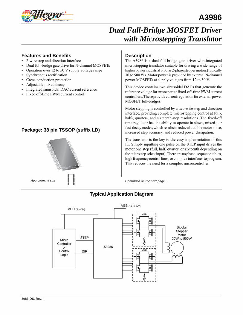
3986-DS, Rev. 1 Features and Benefits ▪ 2-wire step and direction interface ▪ Dual full-bridge gate drive for N-channel MOSFETs ▪ Operation over 12 to 50 V supply voltage range ▪ Synchronous rectification ▪ Cross-conduction protection ▪ Adjustable mixed decay ▪ Integrated sinusoidal DAC current reference ▪ Fixed off-time PWM current control Dual Full-Bridge MOSFET Driver with Microstepping Translator Continued on the next page… Package: 38 pin TSSOP (suffix LD) Typical Application Diagram Approximate size A3986 Description The A3986 is a dual full-bridge gate driver with integrated microstepping translator suitable for driving a wide range of higher power industrial bipolar 2-phase stepper motors (typically 30 to 500 W). Motor power is provided by external N-channel power MOSFETs at supply voltages from 12 to 50 V. This device contains two sinusoidal DACs that generate the reference voltage for two separate fixed-off-time PWM current controllers. These provide current regulation for external power MOSFET full-bridges. Motor stepping is controlled by a two-wire step and direction interface, providing complete microstepping control at full-, half-, quarter-, and sixteenth-step resolutions. The fixed-off time regulator has the ability to operate in slow-, mixed-, or fast-decay modes, which results in reduced audible motor noise, increased step accuracy, and reduced power dissipation. The translator is the key to the easy implementation of this IC. Simply inputting one pulse on the STEP input drives the motor one step (full, half, quarter, or sixteenth depending on the microstep select input). There are no phase-sequence tables, high frequency control lines, or complex interfaces to program. This reduces the need for a complex microcontroller.
Transcript of Dual Full-Bridge MOSFET Driver with Microstepping...
3986-DS, Rev. 1
Features and Benefits▪ 2-wire step and direction interface▪ Dual full-bridge gate drive for N-channel MOSFETs▪ Operation over 12 to 50 V supply voltage range▪ Synchronous rectification▪ Cross-conduction protection▪ Adjustable mixed decay▪ Integrated sinusoidal DAC current reference▪ Fixed off-time PWM current control
Dual Full-Bridge MOSFET Driver with Microstepping Translator
Continued on the next page…
Package: 38 pin TSSOP (suffix LD)
Typical Application Diagram
Approximate size
A3986
DescriptionThe A3986 is a dual full-bridge gate driver with integrated microstepping translator suitable for driving a wide range of higher power industrial bipolar 2-phase stepper motors (typically 30 to 500 W). Motor power is provided by external N-channel power MOSFETs at supply voltages from 12 to 50 V.
This device contains two sinusoidal DACs that generate the reference voltage for two separate fixed-off-time PWM current controllers. These provide current regulation for external power MOSFET full-bridges.
Motor stepping is controlled by a two-wire step and direction interface, providing complete microstepping control at full-, half-, quarter-, and sixteenth-step resolutions. The fixed-off time regulator has the ability to operate in slow-, mixed-, or fast-decay modes, which results in reduced audible motor noise, increased step accuracy, and reduced power dissipation.
The translator is the key to the easy implementation of this IC. Simply inputting one pulse on the STEP input drives the motor one step (full, half, quarter, or sixteenth depending on the microstep select input). There are no phase-sequence tables, high frequency control lines, or complex interfaces to program. This reduces the need for a complex microcontroller.

Dual Full-Bridge MOSFET Driverwith Microstepping TranslatorA3986
2Allegro MicroSystems, Inc.115 Northeast Cutoff, Box 15036Worcester, Massachusetts 01615-0036 (508) 853-5000www.allegromicro.com
The above-supply voltage required for the high-side N-channel
MOSFETs is provided by a bootstrap capacitor. Efficiency is
enhanced by using synchronous rectification and the power FETs
are protected from shoot-through by integrated crossover control
and programmable dead time.
In addition to crossover current control, internal circuit protection provides thermal shutdown with hysteresis and undervoltage lockout. Special power-up sequencing is not required.
This component is supplied in an 38-pin TSSOP (package LD). The package is lead (Pb) free, with 100% matte tin leadframe plating.
Description (continued)
Selection GuidePart Number Packing*
A3986SLD-T Tube, 50 pieces per tubeA3986SLDTR-T Tape and reel, 4000 pieces per reel
*Contact Allegro for additional packing options
Absolute Maximum RatingsCharacteristic Symbol Notes Rating Units
Supply Voltage VBB –0.3 to 50 V
Logic Supply Voltage VDD –0.3 to 7 V
Logic Inputs and Outputs –0.3 to 7 V
SENSEx pins –1 to 1 V
Sxx pins –2 to 55 V
LSSx pins –2 to 5 V
GHxx pins Sxx to Sxx+15 V
GLxx pins –2 to 16 V
Cxx pins –0.3 to Sxx+15 V
Operating Ambient Temperature TA Range S –20 to 85 ºC
Junction Temperature TJ(max) 150 ºC
Storage Temperature Tstg –55 to 150 ºC

Dual Full-Bridge MOSFET Driverwith Microstepping TranslatorA3986
3Allegro MicroSystems, Inc.115 Northeast Cutoff, Box 15036Worcester, Massachusetts 01615-0036 (508) 853-5000www.allegromicro.com
Functional Block Diagram
High-SideDrive
Low-SideDrive
Low-SideDrive
High-SideDrive
PWM LatchBlanking
Mixed Decay
PWM LatchBlanking
Mixed Decay
Protection UVLOTSD
P
P
High-SideDrive
Low-SideDrive
Low-SideDrive
High-SideDrive
P
DAC
DAC
Bandgap Regulator
Phase 1Control Logic
Phase 2Control Logic
VDD VBB
GND
PFD2
ENABLE
RESET
SR
MS2
OSC
ROSC
REF
PFD1
DIR
STEP
MS1
VREG
Phase 1A
Phase 1B
Phase 2A
Phase 2B
CREG
+5 V
C1A
VREG
CBOOT1A
C1B
CBOOT1B
RGH1A
GH1A
GL1A
GL1B
GH1B
S1A
S1B
LSS1
SENSE1
RGL1A
RGH1B
VMOTOR
RGL1B
RSENSE1
C2A
VREF
VREG
VREF
CBOOT2A
C2B
CBOOT2B
RGH2A
GH2A
GL2A
GL2B
GH2B
S2A
S2B
LSS2
SENSE2
RGL2A
RGH2B
VMOTOR
RGL2B
RSENSE2
Bridge1
Bridge2
Phase 1
Phase 2
Translator
VREG
Dual Full-Bridge MOSFET Driverwith Microstepping TranslatorA3986
4Allegro MicroSystems, Inc.115 Northeast Cutoff, Box 15036Worcester, Massachusetts 01615-0036 (508) 853-5000www.allegromicro.com
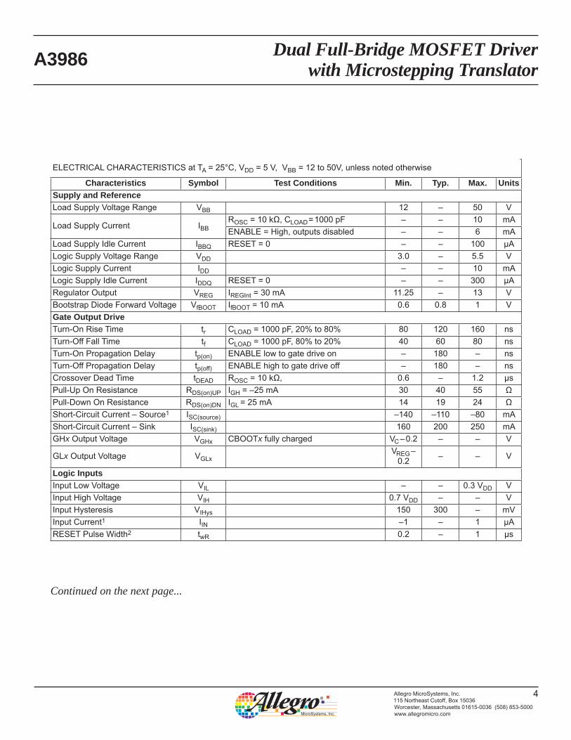
ELECTRICAL CHARACTERISTICS at TA = 25°C, VDD = 5 V, VBB = 12 to 50V, unless noted otherwise
Characteristics Symbol Test Conditions Min. Typ. Max. UnitsSupply and ReferenceLoad Supply Voltage Range VBB 12 – 50 V
Load Supply Current IBBROSC = 10 kΩ, CLOAD = 1000 pF – – 10 mAENABLE = High, outputs disabled – – 6 mA
Load Supply Idle Current IBBQ RESET = 0 – – 100 μALogic Supply Voltage Range VDD 3.0 – 5.5 VLogic Supply Current IDD – – 10 mALogic Supply Idle Current IDDQ RESET = 0 – – 300 μARegulator Output VREG IREGInt = 30 mA 11.25 – 13 VBootstrap Diode Forward Voltage VfBOOT IfBOOT = 10 mA 0.6 0.8 1 VGate Output DriveTurn-On Rise Time tr CLOAD = 1000 pF, 20% to 80% 80 120 160 nsTurn-Off Fall Time tf CLOAD = 1000 pF, 80% to 20% 40 60 80 nsTurn-On Propagation Delay tp(on) ENABLE low to gate drive on – 180 – nsTurn-Off Propagation Delay tp(off) ENABLE high to gate drive off – 180 – nsCrossover Dead Time tDEAD ROSC = 10 kΩ, 0.6 – 1.2 μsPull-Up On Resistance RDS(on)UP IGH = –25 mA 30 40 55 ΩPull-Down On Resistance RDS(on)DN IGL = 25 mA 14 19 24 ΩShort-Circuit Current – Source1 ISC(source) –140 –110 –80 mAShort-Circuit Current – Sink ISC(sink) 160 200 250 mAGHx Output Voltage VGHx CBOOTx fully charged VC – 0.2 – – V
GLx Output Voltage VGLxVREG –
0.2 – – V
Logic InputsInput Low Voltage VIL – – 0.3 VDD VInput High Voltage VIH 0.7 VDD – – VInput Hysteresis VIHys 150 300 – mVInput Current1 IIN –1 – 1 μARESET Pulse Width2 twR 0.2 – 1 μs
Continued on the next page...

Dual Full-Bridge MOSFET Driverwith Microstepping TranslatorA3986
5Allegro MicroSystems, Inc.115 Northeast Cutoff, Box 15036Worcester, Massachusetts 01615-0036 (508) 853-5000www.allegromicro.com
ELECTRICAL CHARACTERISTICS, continued, at TA = 25°C, VDD = 5 V, VBB = 12 to 50V, unless noted otherwiseCharacteristics Symbol Test Conditions Min. Typ. Max. Units
Current ControlBlank Time tBLANK ROSC = 10 kΩ, 1.2 1.5 1.8 μsFixed Off-Time tOFF ROSC = 10 kΩ, , SR= High 18.12 – 23.16 μsReference Input Voltage VREF 0.8 – 2 VInternal Reference Voltage VREFInt 20 kΩ to VDD 1.9 2.0 2.1 VCurrent Trip Point Error3 EITRIP VREF = 2 V – – ±5 %Reference Input Current1 IREF –3 0 3 μAOscillator Frequency fOSC ROSC = 10 kΩ 3.2 4 4.8 MHzProtectionVREG Undervoltage Lockout VREGUV Decreasing VREG 7.5 8 8.5 VVREG Undervoltage Lockout Hysteresis VREGUVHys 100 200 – mV
VDD Undervoltage Lockout VDDUV Decreasing VDD 2.45 2.7 2.95 VVDD Undervoltage Lockout Hysteresis VDDUVHys 50 100 – mV
Overtemperature Shut Down TTSD Temperature increasing – 165 – ºCOvertemperature Shut Down Hysteresis TTSDHys Recovery = TTSD – TTSDHys – 15 – ºC
Control TimingSTEP Low Duration tSTEPL 1 – – μsSTEP High Duration tSTEPH 1 – – μs
Setup Duration tSUInput change to STEP pulse; MS1, MS2, DIR 200 – – ns
Hold Duration tHInput change from STEP pulse; MS1, MS2, DIR 200 – – ns
Wake Time Duration tWAKE 1 – – ms1For input and output current specifications, negative current is defined as coming out of (sourcing) the specified device pin.2A RESET pulse of this duration will reset the translator to the Home position without entering Sleep mode.3Current Trip Point Error is the difference between actual current trip point and the target current trip point, referred to full scale (100%) current: EITRIP = 100 × (ITRIPActual – ITRIPTarget) / IFullScale %

Dual Full-Bridge MOSFET Driverwith Microstepping TranslatorA3986
6Allegro MicroSystems, Inc.115 Northeast Cutoff, Box 15036Worcester, Massachusetts 01615-0036 (508) 853-5000www.allegromicro.com
STEP
t t
tWAKE
RESET
t STEPH t STEPL
SU H
MSx, DIR
Table 1. Microstep Resolution Truth Table
MS2 MS1 Microstep Resolution0 0 Full Step
0 1 Half Step
1 0 Quarter Step
1 1 Sixteenth Step
Table 2. Mixed Decay Selection Truth Table
PFD2 PFD1 Percentage of Fast decay0 0 0% ( ≡ Slow Decay)
0 1 8% (7 cycles)
1 0 26% (23 cycles)
1 1 100% ( ≡ Fast Decay)
Figure 1. Logic Interface Timing Diagram
THERMAL CHARACTERISTICSCharacteristic Symbol Test Conditions* Value Units
Package Thermal Resistance RθJA4-layer PCB, based on JEDEC standard 47 ºC/W
1-layer PCB with copper limited to solder pads 114 ºC/W
*Additional thermal information available on Allegro Web site.

Dual Full-Bridge MOSFET Driverwith Microstepping TranslatorA3986
7Allegro MicroSystems, Inc.115 Northeast Cutoff, Box 15036Worcester, Massachusetts 01615-0036 (508) 853-5000www.allegromicro.com
Home microstep position at Step Angle 45º; DIR = HTable 3. Step Sequencing Settings
FullStep(#)
Half Step(#)
1/4Step(#)
1/16Step(#)
Phase 2Current
(% ITRIP(max))
Phase 1Current
(% ITRIP(max))
Step Angle
(°)
FullStep(#)
Half Step(#)
1/4Step(#)
1/16Step(#)
Phase 2Current
(% ITRIP(max))
Phase 1Current
(% ITRIP(max))
Step Angle
(°)
1 1 1 0.00 100.00 0.0 5 9 33 0.00 –100.00 180.0
2 9.38 100.00 5.6 34 –9.38 –100.00 185.6
3 18.75 98.44 11.3 35 –18.75 –98.44 191.3
4 29.69 95.31 16.9 36 –29.69 –95.31 196.9
2 5 37.50 92.19 22.5 10 37 –37.50 –92.19 202.5
6 46.88 87.50 28.1 38 –46.88 –87.50 208.1
7 56.25 82.81 33.8 39 –56.25 –82.81 213.8
8 64.06 76.56 39.4 40 –64.06 –76.56 219.4
1 2 3 9 70.31 70.31 45.0 3 6 11 41 –70.31 –70.31 225.0
10 76.56 64.06 50.6 42 –76.56 –64.06 230.6
11 82.81 56.25 56.3 43 –82.81 –56.25 236.3
12 87.50 46.88 61.9 44 –87.50 –46.88 241.9
4 13 92.19 37.50 67.5 12 45 –92.19 –37.50 247.5
14 95.31 29.69 73.1 46 –95.31 –29.69 253.1
15 98.44 18.75 78.8 47 –98.44 –18.75 258.8
16 100.00 9.38 84.4 48 –100.00 –9.38 264.4
3 5 17 100.00 0.00 90.0 7 13 49 –100.00 0.00 270.0
18 100.00 –9.38 95.6 50 –100.00 9.38 275.6
19 98.44 –18.75 101.3 51 –98.44 18.75 281.3
20 95.31 –29.69 106.9 52 –95.31 29.69 286.9
6 21 92.19 –37.50 112.5 14 53 –92.19 37.50 292.5
22 87.50 –46.88 118.1 54 –87.50 46.88 298.1
23 82.81 –56.25 123.8 55 –82.81 56.25 303.8
24 76.56 –64.06 129.4 56 –76.56 64.06 309.4
2 4 7 25 70.31 –70.31 135.0 4 8 15 57 –70.31 70.31 315.0
26 64.06 –76.56 140.6 58 –64.06 76.56 320.6
27 56.25 –82.81 146.3 59 –56.25 82.81 326.3
28 46.88 –87.50 151.9 60 –46.88 87.50 331.9
8 29 37.50 –92.19 157.5 16 61 –37.50 92.19 337.5
30 29.69 –95.31 163.1 62 –29.69 95.31 343.1
31 18.75 –98.44 168.8 63 –18.75 98.44 348.8
32 9.38 –100.00 174.4 64 –9.38 100.00 354.4
5 9 33 0.00 –100.00 180.0 1 1 1 0.00 100.00 360.0

Dual Full-Bridge MOSFET Driverwith Microstepping TranslatorA3986
8Allegro MicroSystems, Inc.115 Northeast Cutoff, Box 15036Worcester, Massachusetts 01615-0036 (508) 853-5000www.allegromicro.com
Figure 4. Decay Modes for Quarter-Step Increments
Figure 3. Decay Modes for Half-Step IncrementsFigure 2. Decay Mode for Full-Step Increments
IOUT1B (%*)Phase = 1,Direction = H
IOUT2B (%*)Phase = 2,Direction = H
STEP
Hom
e M
icro
step
Pos
ition
Hom
e M
icro
step
Pos
ition
100
71
–71
0
–100
100
71
–71
0
–100
Slow
Slow
Hom
e M
icro
step
Pos
ition
Hom
e M
icro
step
Pos
ition
100
71
–71
0
–100
100
71
–71
0
–100
STEP
SlowMixed
SlowMixed
SlowMixed
MixedSlow
MixedSlow
MixedSlowSlow
IOUT1B (%*)Phase = 1,Direction = H
IOUT2B (%*)Phase = 2,Direction = H
0
10092
71
38
–38
–71
–92–100
0
10092
71
38
–38
–71
–92–100
Hom
e M
icro
step
Pos
ition
Slow Mixed SlowSlow Mixed
Slow Mixed Slow MixedMixed
STEP
Slow
IOUT1B (%*)Phase = 1,Direction = H
IOUT2B (%*)Phase = 2,Direction = H
*For precise definition of output levels, refer to table 3 *For precise definition of output levels, refer to table 3
*For precise definition of output levels, refer to table 3

Dual Full-Bridge MOSFET Driverwith Microstepping TranslatorA3986
9Allegro MicroSystems, Inc.115 Northeast Cutoff, Box 15036Worcester, Massachusetts 01615-0036 (508) 853-5000www.allegromicro.com
Figure 5. Decay Modes for Sixteenth-Step Increments
MixedSlow MixedSlow
MixedSlow SlowSlow
100968883
–83
7771
63
56
47
38
29
20
10
0
–100–96–88
–77
–71
–63
–56
–47
–38
–29
–20
–10
100968883
–83
7771
63
56
47
38
29
20
10
0
–100–96–88
–77
–71
–63
–56
–47
–38
–29
–20
–10
Hom
e M
icro
step
Pos
ition
Mixed
IOUT1B (%*)Phase = 1,Direction = H
IOUT2B (%*)Phase = 2,Direction = H
STEP
*For precise definition of output levels, refer to table 3

Dual Full-Bridge MOSFET Driverwith Microstepping TranslatorA3986
10Allegro MicroSystems, Inc.115 Northeast Cutoff, Box 15036Worcester, Massachusetts 01615-0036 (508) 853-5000www.allegromicro.com
Functional Description
Basic Operation The A3986 is a complete microstepping FET driver with built-in translator for easy operation with a minimum number of control inputs. It is designed to operate 2-phase bipolar stepper motors in full-, half-, quarter, and sixteenth-step modes. The current in each of the two external power full-bridges, all N-channel MOSFETs, is independently regulated by a fixed off-time PWM control circuit. The full-bridge current at each step is set by the value of an external cur-rent sense resistor, RSENSEX , in the ground connection to the bridge, a reference voltage, VREF, and the output of the DAC controlled by the translator.The use of PWM with N-channel MOSFETs provides the most cost-effective solution for a high efficiency motor drive. The A3986 provides all the necessary circuits to ensure that the gate-source voltage of both high-side and low-side external MOSFETs are above 10 V, and that there is no cross-conduction (shoot through) in the external bridge.Specific functions are described more fully in the following sections.Power SuppliesTwo power connections are required. The motor power sup-ply should be connected to VBB to provide the gate drive levels. Power for internal logic is provided by the VDD input. Internal logic is designed to operate from 3 to 5.5 V, allowing the use of 3.3 or 5 V external logic interface cir-cuits.
GND The ground pin is a reference voltage for internal logic and analog circuits. There is no large current flow through this pin. To avoid any noise from switching circuits, this should have an independent trace to the supply ground star point.
VREG The voltage at this pin is generated by a low-drop-out linear regulator from the VBB supply. It is used to oper-ate the low-side gate drive outputs, GLxx, and to provide the charging current for the bootstrap capacitors, CBOOTx. To limit the voltage drop when the charge current is pro-vided, this pin should be decoupled with a ceramic capaci-tor, CREG, to ground. The value CREG should typically
be 40 times the value of the bootstrap capacitor for PWM frequencies up to 14 kHz. Above 14 kHz, the minimum recommended value can be determined from the following formula:
CREG > CBOOT × 3 × fPWM ,
where CREG and CBOOT are in nF, and fPWM is the maximum PWM frequency, in kHz. VREG is monitored, and if the volt-age becomes too low, the outputs will be disabled.
REF The reference voltage, VREF, at this pin sets the maximum (100%) peak current. The REF input is internally limited to 2 V when a 20 kΩ pull-up resistor is connected between VREF and VDD. This allows the maximum refer-ence voltage to be set without the need for an externally-generated voltage. An external reference voltage below the maximum can also be input on this pin. The voltage at VREF is divided by 8 to produce the DAC reference voltage level.
OSC The internal FET control timing is derived from a master clock running at 4 MHz typical. A resistor, ROSC, connected from the OSC pin to GND sets the frequency (in MHz) to approximately:
fOSC ≈ 100 / (6 + 1.9 × ROSC) ,
where ROSC, in kΩ, is typically between 50 kΩ and 10 kΩ. The master oscillator period is used to derive the PWM off-time, dead time, and blanking time.
Gate DriveThe A3986 is designed to drive external power N-channel MOSFETs. It supplies the transient currents necessary to quickly charge and discharge the external FET gate capaci-tance in order to reduce dissipation in the external FET during switching. The charge and discharge rate can be controlled using an external resistor , RGx, in series with the connection to the gate of the FET. Cross-conduction is prevented by the gate drive circuits which introduce a dead time, tDEAD , between switching one FET off and the comple-mentary FET on. tDEAD is at least 3 periods of the master oscillator but can be up to 1 cycle longer to allow oscillator synchronization.

Dual Full-Bridge MOSFET Driverwith Microstepping TranslatorA3986
11Allegro MicroSystems, Inc.115 Northeast Cutoff, Box 15036Worcester, Massachusetts 01615-0036 (508) 853-5000www.allegromicro.com
C1A, C1B, C2A, and C2B High-side connections for the bootstrap capacitors, CBOOTx, and positive supply for high-side gate drivers. The bootstrap capacitors are charged to approximately VREG when the associated output Sxx terminal is low. When the output swings high, the voltage on this ter-minal rises with the output to provide the boosted gate volt-age needed for the high-side N-channel power MOSFETs. The bootstrap capacitor should be ceramic and have a value of 10 to 20 times the total MOSFET gate capacitance.
GH1A, GH1B, GH2A, and GH2B High-side gate drive outputs for external N-channel MOSFETs. External series gate resistors can be used to control the slew rate seen at the gate, thereby controlling the di/dt and dv/dt at the motor terminals. GHxx = 1 (high) means that the upper half of the driver is turned on and will source current to the gate of the high-side MOSFET in the external motor-driving bridge. GHxx = 0 (low) means that the lower half of the driver is turned on and will sink current from the external MOSFET’s gate circuit to the respective Sxx pin.
S1A, S1B, S2A, and S2B Directly connected to the motor, these terminals sense the voltages switched across the load and define the negative supply for the floating high-side drivers. The discharge current from the high-side MOSFET gate capacitance flows through these connections which should have low impedance traces to the MOSFET bridge.
GL1A, GL1B, GL2A, and GL2B Low-side gate drive outputs for external N-channel MOSFETs. External series gate resistors (as close as possible to the MOSFET gate) can be used to reduce the slew rate seen at the gate, thereby controlling the di/dt and dv/dt at the motor terminals. GLxx = 1 (high) means that the upper half of the driver is turned on and will source current to the gate of the low-side MOSFET in the external motor-driving bridge. GLxx = 0 (low) means that the lower half of the driver is turned on and will sink current from the gate of the external MOSFET to the LSSx pin.
LSS1 and LSS2 Low-side return path for discharge of the gate capacitors, connected to the common sources of the low-side external FETs through low-impedance traces.
Motor ControlMotor speed and direction is controlled simply by two logic inputs, and the microstep level is controlled by a further two logic inputs. At power-up or reset, the translator sets the DACs and phase current polarity to the initial Home state (see figures 2 through 5 for home-state conditions), and sets the current regulator for both phases to mixed-decay mode. When a step command signal occurs on the STEP input, the translator automatically sequences the DACs to the next level (see table 3 for the current level sequence and current polarity).
The microstep resolution is set by inputs MS1 and MS2 as shown in table 1. If the new DAC level is higher or equal to the previous level, then the decay mode for that full-bridge will be slow decay. If the new DAC output level is lower than the previous level, the decay mode for that full-bridge will be set by the PFD1 and PFD2 inputs. This automatic current-decay selection improves microstepping performance by reducing the distortion of the current waveform due to the motor BEMF.
STEP A low-to-high transition on the STEP input sequences the translator and advances the motor one increment. The translator controls the input to the DACs as well as the direc-tion of current flow in each winding. The size of the incre-ment is determined by the state of the MSx inputs.
MS1 and MS2 These Microstep Select inputs are used to select the microstepping format, per table 1. Changes to these inputs do not take effect until the next STEP input ris-ing edge.
DIR This Direction input determines the direction of rotation of the motor. When low, the direction is “clockwise” and “counterclockwise” when high. A change on this input does not take effect until the next STEP rising edge.
Internal PWM Current ControlEach full-bridge is independently controlled by a fixed off-time PWM current control circuit that limits the load current in the phase to a desired value, ITRIP. Initially, a diagonal pair

Dual Full-Bridge MOSFET Driverwith Microstepping TranslatorA3986
12Allegro MicroSystems, Inc.115 Northeast Cutoff, Box 15036Worcester, Massachusetts 01615-0036 (508) 853-5000www.allegromicro.com
of source and sink MOSFETs are enabled and current flows through the motor winding and the current sense resistor, RSENSEx. When the voltage across RSENSEx equals the DAC output voltage, the current sense comparator resets the PWM latch, which turns off the source MOSFET (slow decay mode) or the sink and source MOSFETs (fast decay mode). The maximum value of current limiting is set by the selection of RSENSE and the voltage at the REF input, with a transconductance function approximated by:
ITRIP(max) = VREF / (8 × RSENSE )
The DAC, controlled by the translator, reduces the refer-ence voltage, VREF , in precise steps to produce the required sinusoidal reference levels for the current sense comparator. This limits the phase current trip level, ITRIP, to a portion of the maximum current level, ITRIP(max), defined by:
ITRIP = (% ITRIP(max) / 100) × ITRIP(max)
See table 3 for % ITRIP(max) at each step.
Fixed Off-Time The internal PWM current control circuitry uses the master oscillator to control the length of time the power MOSFETs remain off. The off-time, tOFF , is nominally 87 cycles of the master oscillator (21.75 μs at 4 MHz), but may be up to 1 cycle longer to synchronize with the master oscillator.
Blanking This function blanks the output of the current sense comparator when the outputs are switched by the internal current control. The comparator output is blanked to prevent false overcurrent detection due to reverse recovery currents of the clamp diodes and switching transients related to the capacitance of the load. The blank time, tBLANK , is 6 cycles of the master oscillator (1.5 μs at 4 MHz). Because the tBLANK follows after the end of tOFF, no synchronization error occurs.
Dead Time To prevent cross-conduction (shoot through) in the power full-bridge, a dead time is introduced between switching one MOSFET off and switching the complemen-tary MOSFET on. The dead time, tDEAD, is 3 cycles of the master oscillator (750 ns at 4MHz), but may be up to 1 cycle longer to synchronize with the master oscillator.
ENABLE This input simply turns off all the power MOSFETs. When set at logic high, the outputs are disabled. When set at logic low, the internal control enables the out-puts as required. Inputs to the translator (STEP, DIR, MS1, and MS2) and the internal sequencing logic are all active independent of the ENABLE input state.
RESET An active-low control input used to minimize power consumption when not in use. This disables much of the internal circuitry, including the output MOSFETs and internal regulator. When set at logic high, allows normal operation and start-up of the device in the home position. When coming out of sleep mode, wait 1 ms before issuing a STEP command, to allow the internal regulator to stabilize. The outputs can also be reset to the home position without entering sleep mode. To do so, pulse the RESET input low, with a pulse width between twR(min) and twR(max).
Mixed Decay OperationMixed decay is a technique that provides greater control of phase currents while the current is decreasing. When a stepper motor is driven at high speed, the back EMF from the motor will lag behind the driving current. If a passive current decay mode, such as slow decay, is used in the cur-rent control scheme, then the motor back EMF can cause the phase current to rise out of control. Mixed decay eliminates this effect by putting the full-bridge initially into fast decay, and then switching to slow decay after some time. Because fast decay is an active (driven) decay mode, this portion of the current decay cycle will ensure that the current remains in control. Using fast decay for the full current decay time (off-time) would result in a large ripple current, but switch-ing to slow decay once the current is in control will reduce the ripple current value. The portion of the off-time that the full-bridge has to remain in fast decay will depend on the characteristics and the speed of the motor.
When the phase current is rising, the motor back EMF will not affect the current control and slow decay may be used to minimize the phase current ripple. The A3986 automatically switches between slow decay, when the current is rising, and mixed decay, when the current is falling. The portion of the off-time that the full-bridge remains in fast decay is defined by the PFD1 and PFD2 inputs.

Dual Full-Bridge MOSFET Driverwith Microstepping TranslatorA3986
13Allegro MicroSystems, Inc.115 Northeast Cutoff, Box 15036Worcester, Massachusetts 01615-0036 (508) 853-5000www.allegromicro.com
PFD1 and PFD2 The Percent Fast Decay pins are used to select the portion of fast decay, according to table 2, to be used when mixed decay is enabled. Mixed decay is enabled when a STEP input signal commands an output current that is lower than for the previous step. In mixed decay mode, as the trip point is reached, the A3986 goes into fast decay mode until the specified number of master oscillator cycles has completed. After this fast decay portion, the A3986 switches to slow decay mode for the remainder of the fixed off-time, tOFF.
Using PFD1 and PFD 2 to select 0% fast decay will effec-tively maintain the full-bridge in slow decay at all times. This option can be used to keep the phase current ripple to a minimum when the motor is stationary or stepping at very low rates.
Selecting 100% fast decay will provide the fastest current control when the current is falling and can help when the motor is being driven at very high step rates.
SR Input used to set synchronous rectification mode. When a PWM off-cycle is triggered, load current recirculates according to the decay mode selected by the control logic. The synchronous rectification feature turns on the appropri-ate MOSFETs during the current decay and effectively shorts
out the body diodes with the low RDS(ON) of the MOSFET. This lowers power dissipation significantly and eliminates the need for additional Schottky diodes. Synchronous rectification can be set to either active mode or disabled mode.
• Active Mode When the SR pin input is logic low, active mode is enabled and synchronous rectification will occur. This mode prevents reversal of the load current by turning off synchronous rectification when a zero current level is detected. This prevents the motor winding from conduct-ing in the reverse direction.
• Disabled Mode When the SR pin input is logic high, syn-chronous rectification is disabled. This mode is typically used when external diodes are required to transfer power dissipation from the power MOSFETs to external, usually Schottky, diodes.
Shutdown Operation In the event of an overtempera-ture fault, or an undervoltage fault on VREG, the MOS-FETs are disabled until the fault condition is removed. At power-up, and in the event of low voltage at VDD, the under voltage lockout (UVLO) circuit disables the MOSFETs until the voltage at VDD reaches the minimum level. Once VDD is above the minimum level, the translator is reset to the home state, and the MOSFETs are reenabled.

Dual Full-Bridge MOSFET Driverwith Microstepping TranslatorA3986
14Allegro MicroSystems, Inc.115 Northeast Cutoff, Box 15036Worcester, Massachusetts 01615-0036 (508) 853-5000www.allegromicro.com
Applications Information
Current SensingTo minimize inaccuracies in sensing the IPEAK current level caused by ground-trace IR drops, the sense resistor, RSENSEx, should have an independent return to the supply ground star point. For low-value sense resistors, the IR drops in the sense resistor PCB traces can be significant and should be taken into account. The use of sockets should be avoided as they can introduce variation in RSENSEx due to their con-tact resistance.
Thermal ProtectionAll drivers are turned off when the junction temperature reaches 165°C typical. This is intended only to protect the A3986 from failures due to excessive junction temperatures. Thermal protection will not protect the A3986 from continu-ous short circuits. Thermal shutdown has a hysteresis of approximately 15°C.
Circuit Layout Because this is a switch-mode application, where rapid cur-rent changes are present, care must be taken during layout of the application PCB. The following points are provided as guidance for layout. Following all guidelines will not always be possible. However, each point should be carefully consid-ered as part of any layout procedure.
Ground connection layout recommendations:
1. Decoupling capacitors for the supply pins VBB, VREG, and VDD should be connected independently close to the GND pin and not to any ground plane. The decoupling capacitors should also be connected as close as possible to the corresponding supply pin.
2. The oscillator timing resistor ROSC should be connected to the GND pin. It should not be connected to any ground plane, supply common, or the power ground.
3. The GND pin should be connected by an independent low impedance trace to the supply common at a single point.
4. Check the peak voltage excursion of the transients on the LSS pin with reference to the GND pin using a close grounded (tip and barrel) probe. If the voltage at LSS exceeds the absolute maximum specified in this datasheet, add additional clamping, capacitance, or both between the LSS pin and the AGND pin.
Other layout recommendations:
1. Gate charge drive paths and gate discharge return paths may carry transient current pulses. Therefore, the traces from GHxx, GLxx, Sxx, and LSSx should be as short as possible to reduce the inductance of the circuit trace.
2. Provide an independent connection from each LSS pin to the common point of each power bridge. It is not recom-mended to connect LSS directly to the GND pin. The LSS connection should not be used for the SENSE connection.
3. Minimize stray inductance by using short, wide copper runs at the drain and source terminals of all power FETs. This includes motor lead connections, the input power bus, and the common source of the low-side power FETs. This will minimize voltages induced by fast switching of large load currents.
4. Consider the use of small (100 nF) ceramic decoupling capacitors across the source and drain of the power FETs to limit fast transient voltage spikes caused by trace inductance.
The above are only recommendations. Each application is different and may encounter different sensitivities. Each design should be tested at the maximum current, to ensure any parasitic effects are eliminated.

Dual Full-Bridge MOSFET Driverwith Microstepping TranslatorA3986
15Allegro MicroSystems, Inc.115 Northeast Cutoff, Box 15036Worcester, Massachusetts 01615-0036 (508) 853-5000www.allegromicro.com
Terminal List TableNumber Name Description
1 C2A Phase 2 bootstrap capacitor drive A connection2 GH2A Phase 2 high-side gate drive A3 S2A Phase 2 motor connection A4 GL2A Phase 2 low-side gate drive A5 NC No internal connection6 VREG Regulator decoupling capacitor connection7 VBB Motor supply voltage8 GL1A Phase 1 low-side gate drive A9 S1A Phase 1 motor connection A10 GH1A Phase 1 high-side gate drive A11 C1A Phase 1 bootstrap capacitor drive A connection12 C1B Phase 1 bootstrap capacitor drive B connection13 GH1B Phase 1 high-side gate drive B14 S1B Phase 1 motor connection B15 GL1B Phase 1 low-side gate drive B16 LSS1 Phase 1 low-side source connection17 SENSE1 Phase 1 bridge current sense input18 SR Synchronous rectification enable19 ENABLE Output enable20 GND Ground21 REF Reference voltage22 RESET Reset input23 OSC Oscillator input, ROSC resistor connection24 NC No internal connection25 VDD Logic supply voltage26 STEP Step input27 PFD2 Percent Fast Decay input 228 MS1 Microstep Select input 129 MS2 Microstep Select input 230 DIR Direction input31 PFD1 Percent Fast Decay input 132 SENSE2 Phase 2 bridge current sense input33 LSS2 Phase 2 low-side source connection34 NC No internal connection35 GL2B Phase 2 low-side gate drive B36 S2B Phase 2 motor connection B37 GH2B Phase 2 high-side gate drive B38 C2B Phase 2 bootstrap capacitor drive B connection
7
8
9
10
11
12
13
6
5
30
29
28
27
26
25
24
31
32
15
16
17
18
14
1
2
3
4
22
21
2019
23
36
35
38
37
34
33
SENSE2
PFD1
DIR
MS2
MS1
PFD2
STEP
VDD
NC
NC
VREG
VBB
GL1A
S1A
GH1A
C1A
C1B
GH1B
S1B
GL1B
LSS1
SENSE1
SR
ENABLE
C2A
GH2A
S2A
GL2A
S2B
GL2B
NC
LSS2
OSC
RESET
REF
GND
GH2B
C2B
ControlLogic
Translator
Pin-out Diagram

Dual Full-Bridge MOSFET Driverwith Microstepping TranslatorA3986
16Allegro MicroSystems, Inc.115 Northeast Cutoff, Box 15036Worcester, Massachusetts 01615-0036 (508) 853-5000www.allegromicro.com
LD Package, 38-Pin TSSOP
A
1.20MAX
.047
0.150.00
.006
.000
0.270.17
.011
.007
4.5 4.3
.177 .169
6.6 6.2
.260 .244
0.200.09
.008
.004
8º0º
0.750.45
.030
.018
1REF
.039
9.8 9.6
.386
.378
CSEATINGPLANE
AB
38X
0.08 [.003] M C A B
C0.10 [.004]38X
0.50 .020
0.25 .010
5.9NOM
.232
0.30NOM
.012 36X 0.20MIN
.0080.50NOM
.0201.85NOM
.073
21
38
GAUGE PLANESEATING PLANE
A Terminal #1 mark area
Preliminary dimensions, for reference only(reference JEDEC MO-153 BD-1)Dimensions in millimetersU.S. Customary dimensions (in.) in brackets, for reference onlyDimensions exclusive of mold flash, gate burrs, and dambar protrusions Exact case and lead configuration at supplier discretion within limits shown
B Reference land pattern layout (reference IPC7351 TSSOP50P640X120-38M); adjust as necessary to meet application process requirements and PCB layout tolerances
38
21
B
Copyright ©2005, 2007, Allegro MicroSystems, Inc.The products described here are manufactured under one or more U.S. patents or U.S. patents pending. Allegro MicroSystems, Inc. reserves the right to make, from time to time, such de par tures from the detail spec i fi ca tions as may be required to per-
mit improvements in the per for mance, reliability, or manufacturability of its products. Before placing an order, the user is cautioned to verify that the information being relied upon is current.
Allegro’s products are not to be used in life support devices or systems, if a failure of an Allegro product can reasonably be expected to cause the failure of that life support device or system, or to affect the safety or effectiveness of that device or system.
The in for ma tion in clud ed herein is believed to be ac cu rate and reliable. How ev er, Allegro MicroSystems, Inc. assumes no re spon si bil i ty for its use; nor for any in fringe ment of patents or other rights of third parties which may result from its use.
For the latest version of this document, visit our website:www.allegromicro.com