DSP Exciter (EC) User Manual - Repeater Builder...This manual provides information for the Glenayre...
76
Print Date: 06/10/98 Copyright © 1998 Glenayre DSP Exciter Rev. B: 06/11/98 Specifications subject to change without notice Copyright © 1998 Glenayre All rights reserved. No part of this work may be reproduced or copied in any form or by any means -- graphic, electronic, or mechanical, including photocopying, recording, taping, or information-retrieval system -- without written permission of Glenayre. DSP Exciter (EC) User Manual RELEASED PN 9110.01021 Revision B
Transcript of DSP Exciter (EC) User Manual - Repeater Builder...This manual provides information for the Glenayre...
Print Date: 06/10/98 Copyright © 1998 Glenayre
DSP Exciter Rev. B: 06/11/98
Specifications subject to change without notice
Copyright © 1998 Glenayre
All rights reserved. No part of this work may be reproduced or copied in any form or by any means -- graphic, electronic, or mechanical, including photocopying, recording, taping, or information-retrieval system -- without written permission of Glenayre.
DSP Exciter (EC)
User Manual
RELEASED
PN 9110.01021
Revision B
DSP Exciter Glenayre Document Number: 9110.01021Document Change Record Rev. B: 06/11/98
Copyright © 1998 Glenayre Print Date: 06/10/98
Document Change Record
Issue: 1, Revision A
Date: 11/24/97
Changes: None, Original
Issue: 1, Revision B
Date: 06/11/98
Changes: made 88-us changes to text and figures, created intdex
Glenayre Document Number: 9110.01021 DSP ExciterRev. B: 06/11/98 Table of Contents
d102
1_ti.
toc
Print Date: 06/10/98 Copyright © 1998 Glenayre Page: -i
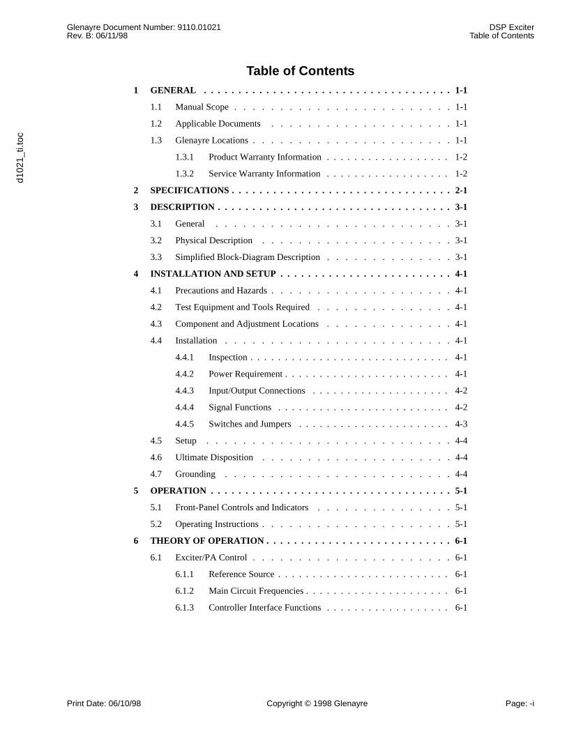
Table of Contents1 GENERAL . . . . . . . . . . . . . . . . . . . . . . . . . . . . . . . . . . . . 1-1
1.1 Manual Scope . . . . . . . . . . . . . . . . . . . . . . . . 1-1
1.2 Applicable Documents . . . . . . . . . . . . . . . . . . . . 1-1
1.3 Glenayre Locations . . . . . . . . . . . . . . . . . . . . . . 1-1
1.3.1 Product Warranty Information . . . . . . . . . . . . . . . . . . 1-2
1.3.2 Service Warranty Information . . . . . . . . . . . . . . . . . . 1-2
2 SPECIFICATIONS . . . . . . . . . . . . . . . . . . . . . . . . . . . . . . . . 2-1
3 DESCRIPTION . . . . . . . . . . . . . . . . . . . . . . . . . . . . . . . . . . 3-1
3.1 General . . . . . . . . . . . . . . . . . . . . . . . . . . 3-1
3.2 Physical Description . . . . . . . . . . . . . . . . . . . . . 3-1
3.3 Simplified Block-Diagram Description . . . . . . . . . . . . . . 3-1
4 INSTALLATION AND SETUP . . . . . . . . . . . . . . . . . . . . . . . . . 4-1
4.1 Precautions and Hazards . . . . . . . . . . . . . . . . . . . . 4-1
4.2 Test Equipment and Tools Required . . . . . . . . . . . . . . . 4-1
4.3 Component and Adjustment Locations . . . . . . . . . . . . . . 4-1
4.4 Installation . . . . . . . . . . . . . . . . . . . . . . . . . 4-1
4.4.1 Inspection . . . . . . . . . . . . . . . . . . . . . . . . . . . . . 4-1
4.4.2 Power Requirement . . . . . . . . . . . . . . . . . . . . . . . . 4-1
4.4.3 Input/Output Connections . . . . . . . . . . . . . . . . . . . . 4-2
4.4.4 Signal Functions . . . . . . . . . . . . . . . . . . . . . . . . . 4-2
4.4.5 Switches and Jumpers . . . . . . . . . . . . . . . . . . . . . . 4-3
4.5 Setup . . . . . . . . . . . . . . . . . . . . . . . . . . . 4-4
4.6 Ultimate Disposition . . . . . . . . . . . . . . . . . . . . . 4-4
4.7 Grounding . . . . . . . . . . . . . . . . . . . . . . . . . 4-4
5 OPERATION . . . . . . . . . . . . . . . . . . . . . . . . . . . . . . . . . . . 5-1
5.1 Front-Panel Controls and Indicators . . . . . . . . . . . . . . . 5-1
5.2 Operating Instructions . . . . . . . . . . . . . . . . . . . . . 5-1
6 THEORY OF OPERATION . . . . . . . . . . . . . . . . . . . . . . . . . . . 6-1
6.1 Exciter/PA Control . . . . . . . . . . . . . . . . . . . . . . 6-1
6.1.1 Reference Source . . . . . . . . . . . . . . . . . . . . . . . . . 6-1
6.1.2 Main Circuit Frequencies . . . . . . . . . . . . . . . . . . . . . 6-1
6.1.3 Controller Interface Functions . . . . . . . . . . . . . . . . . . 6-1
DSP Exciter Glenayre Document Number: 9110.01021Table of Contents Rev. B: 06/11/98
Page: -ii Copyright © 1998 Glenayre Print Date: 06/10/98
6.2 Interface to Controller . . . . . . . . . . . . . . . . . . . . 6-1
6.3 DSP Modulator . . . . . . . . . . . . . . . . . . . . . . . 6-3
6.3.1 General . . . . . . . . . . . . . . . . . . . . . . . . . . . . . . 6-3
6.3.2 DSP Modulator Signal Flow . . . . . . . . . . . . . . . . . . . 6-3
6.3.2.1 Digital Signal Modulator . . . . . . . . . . . . . . . 6-3
6.3.2.2 Digital Quadrature Modulator . . . . . . . . . . . . 6-4
6.3.2.3 Digital-to-Analog Converter . . . . . . . . . . . . . 6-4
6.3.2.4 Read-Only Memory . . . . . . . . . . . . . . . . . 6-4
6.4 IF Stage . . . . . . . . . . . . . . . . . . . . . . . . . . 6-4
6.4.1 Filter-1 . . . . . . . . . . . . . . . . . . . . . . . . . . . . . . 6-4
6.4.2 Mixer-1 . . . . . . . . . . . . . . . . . . . . . . . . . . . . . . 6-6
6.4.3 Filter-2 . . . . . . . . . . . . . . . . . . . . . . . . . . . . . . 6-6
6.4.4 VCO-1 . . . . . . . . . . . . . . . . . . . . . . . . . . . . . . 6-6
6.4.5 Synthesizer-1 . . . . . . . . . . . . . . . . . . . . . . . . . . . 6-6
6.5 MCU . . . . . . . . . . . . . . . . . . . . . . . . . . . 6-6
6.5.1 Microcontroller Unit (MCU) . . . . . . . . . . . . . . . . . . . 6-7
6.5.2 Digital-to-Analog (D/A) Converter . . . . . . . . . . . . . . . 6-7
6.5.3 8/16-Bit Converter . . . . . . . . . . . . . . . . . . . . . . . . 6-7
6.5.4 Read-Only Memory . . . . . . . . . . . . . . . . . . . . . . . 6-8
6.5.5 VSWR-Fault Detector . . . . . . . . . . . . . . . . . . . . . . 6-8
6.5.6 Alarm Data-to-Logic Conversion . . . . . . . . . . . . . . . . 6-8
6.5.7 Alarm Data-to-Logic Conversion . . . . . . . . . . . . . . . . 6-8
6.6 RF Assemblies . . . . . . . . . . . . . . . . . . . . . . 6-14
6.6.1 RF Stage Location . . . . . . . . . . . . . . . . . . . . . . . 6-14
6.6.2 RF Assemblies . . . . . . . . . . . . . . . . . . . . . . . . . 6-14
6.6.2.1 RF Stage Description . . . . . . . . . . . . . . . . 6-14
6.6.2.2 RF Stage Bands . . . . . . . . . . . . . . . . . . . 6-14
6.6.2.3 RF Stage Signal Flow . . . . . . . . . . . . . . . . 6-14
6.6.2.3.1 Mixer-2 . . . . . . . . . . . . . . . . . . . . . . . . 6-14
6.6.2.3.2 Filter . . . . . . . . . . . . . . . . . . . . . . . . . . . 6-15
6.6.2.3.3 Amplifier . . . . . . . . . . . . . . . . . . . . . . . 6-15
6.6.2.3.4 VCO-2 . . . . . . . . . . . . . . . . . . . . . . . . . 6-15
6.6.2.3.5 Synthesizer-2 . . . . . . . . . . . . . . . . . . . . 6-15
6.7 Voltage Regulator Circuit . . . . . . . . . . . . . . . . . . 6-15
Glenayre Document Number: 9110.01021 DSP ExciterRev. B: 06/11/98 Table of Contents
d102
1_ti.
toc
Print Date: 06/10/98 Copyright © 1998 Glenayre Page: -iii
7 MAINTENANCE . . . . . . . . . . . . . . . . . . . . . . . . . . . . . . . . . 7-1
7.1 Location of Maintenance Procedures . . . . . . . . . . . . . . . 7-1
7.2 Test Equipment Required . . . . . . . . . . . . . . . . . . . 7-1
7.3 VCO-2 Adjustment Procedure . . . . . . . . . . . . . . . . . 7-1
7.3.1 VCO-2 Multichannel Adjustment Procedure . . . . . . . . . . 7-1
7.3.2 VCO-2 Single-Channel Adjustment Procedure . . . . . . . . . 7-1
7.4 Over-The-Link Downloading . . . . . . . . . . . . . . . . . . 7-2
7.5 On-The-Fly Channel/Mode Changing . . . . . . . . . . . . . . 7-2
7.5.1 Programming Example . . . . . . . . . . . . . . . . . . . . . . 7-3
7.5.1.1 DSP Exciter (2.1) / GL-C2000 (2.3) . . . . . . . . . 7-4
7.5.1.2 DSP Exciter (3.0) / GL-C2000 (3.0) / GL3000 (6.0) . 7-4
7.6 16-Channel Operation . . . . . . . . . . . . . . . . . . . . . 7-4
7.7 On-The-Fly Interface . . . . . . . . . . . . . . . . . . . . . 7-5
7.8 Checkout . . . . . . . . . . . . . . . . . . . . . . . . . . 7-6
7.9 Troubleshooting . . . . . . . . . . . . . . . . . . . . . . . 7-6
8 REMOVAL AND REINSTALLATION . . . . . . . . . . . . . . . . . . . . 8-1
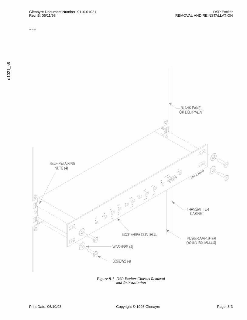
8.1 Exciter/PA Control Chassis . . . . . . . . . . . . . . . . . . . 8-1
8.1.1 Removal Procedure . . . . . . . . . . . . . . . . . . . . . . . . 8-1
8.1.2 Reinstallation Procedure . . . . . . . . . . . . . . . . . . . . . 8-1
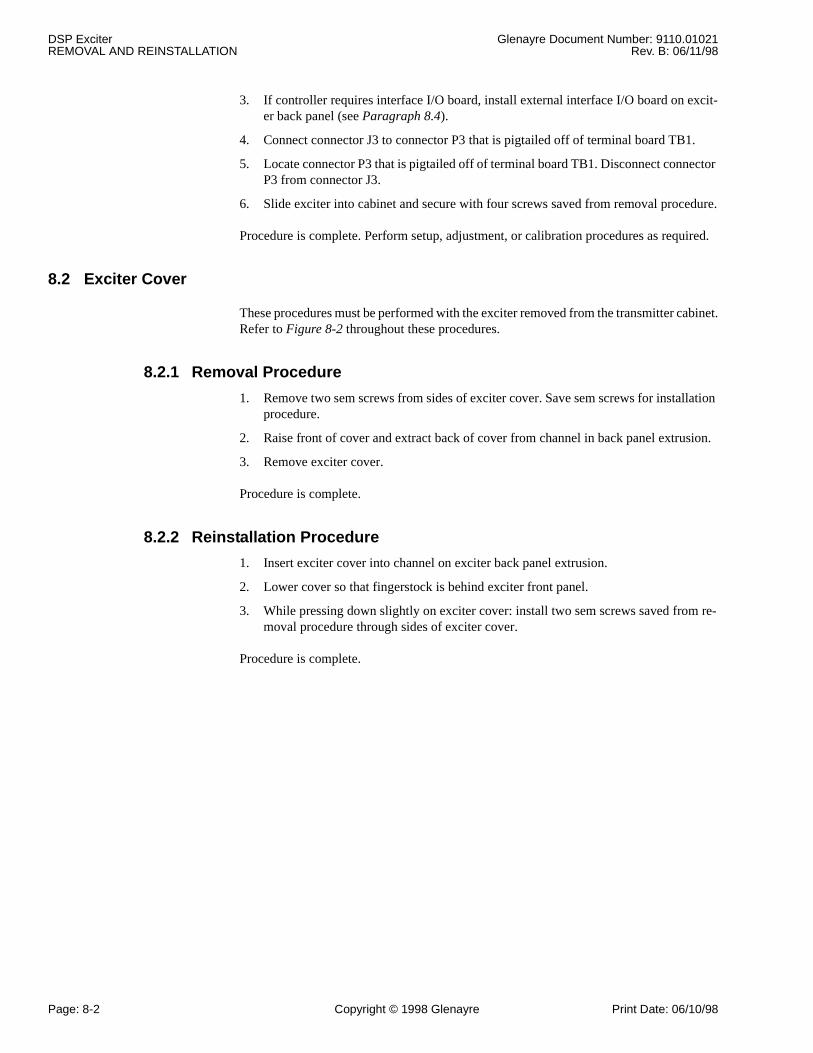
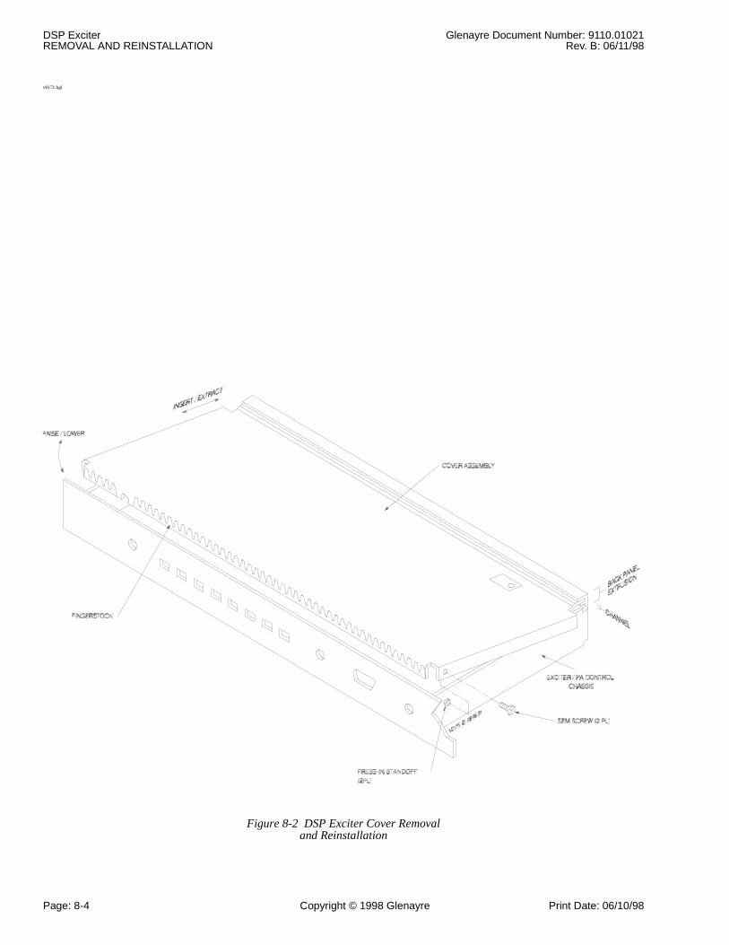
8.2 Exciter Cover . . . . . . . . . . . . . . . . . . . . . . . . 8-2
8.2.1 Removal Procedure . . . . . . . . . . . . . . . . . . . . . . . . 8-2
8.2.2 Reinstallation Procedure . . . . . . . . . . . . . . . . . . . . . 8-2
8.3 Exciter/Control Board . . . . . . . . . . . . . . . . . . . . . 8-5
8.3.1 Removal Procedure . . . . . . . . . . . . . . . . . . . . . . . . 8-5
8.3.2 Reinstallation Procedure . . . . . . . . . . . . . . . . . . . . . 8-5
8.4 Interface I/O Board . . . . . . . . . . . . . . . . . . . . . . 8-8
8.4.1 Removal Procedure . . . . . . . . . . . . . . . . . . . . . . . . 8-8
8.4.2 Reinstallation Procedure . . . . . . . . . . . . . . . . . . . . . 8-8
8.5 VCO/RF Amplifier Board . . . . . . . . . . . . . . . . . . . 8-9
8.5.1 Removal Procedure . . . . . . . . . . . . . . . . . . . . . . . . 8-9
8.5.2 Reinstallation Procedure . . . . . . . . . . . . . . . . . . . . . 8-9
DSP Exciter Glenayre Document Number: 9110.01021Table of Contents Rev. B: 06/11/98
Page: -iv Copyright © 1998 Glenayre Print Date: 06/10/98
9 OPTIONS . . . . . . . . . . . . . . . . . . . . . . . . . . . . . . . . . . . . . 9-1
9.1 Exciter/PA Control w/ QT-1000 Interface . . . . . . . . . . . . 9-1
9.1.1 Reference Source . . . . . . . . . . . . . . . . . . . . . . . . . 9-1
9.1.2 Controller Interface Connector Functions (QT-1000) . . . . . . 9-1
9.1.3 Interface Conversion Functions (QT-1000) . . . . . . . . . . . 9-1
9.1.3.1 Analog-Mode A/D Conversion . . . . . . . . . . . 9-1
9.1.3.2 FSK-Data-Bit Strapping . . . . . . . . . . . . . . . 9-2
9.1.3.3 Channel-Select-Bit Strapping . . . . . . . . . . . . 9-2
9.1.3.4 Mode-Select-Bit Strapping . . . . . . . . . . . . . . 9-2
9.1.3.5 Power Sample D/A Conversion . . . . . . . . . . . 9-2
9.2 Exciter/PA Control with Standard Interface . . . . . . . . . . . . 9-5
9.2.1 Reference Source . . . . . . . . . . . . . . . . . . . . . . . . . 9-5
9.2.2 Controller Interface Connector Functions (Standard) . . . . . . 9-5
9.2.3 Interface Conversion Functions (Standard) . . . . . . . . . . . 9-5
9.2.3.1 Analog-Mode A/D Conversion . . . . . . . . . . . 9-5
9.2.3.2 FSK-Data-Bit Strapping . . . . . . . . . . . . . . . 9-6
9.2.3.3 Channel-Select-Bit Strapping . . . . . . . . . . . . 9-6
9.2.3.4 Mode-Select-Bit Strapping . . . . . . . . . . . . . . 9-6
9.2.3.5 Power Sample D/A Conversion . . . . . . . . . . . 9-6
9.3 Exciter/PA Control with I20 Interface . . . . . . . . . . . . . . 9-6
9.3.1 Reference Source . . . . . . . . . . . . . . . . . . . . . . . . . 9-6
9.3.2 Controller Interface Connector Functions . . . . . . . . . . . . 9-7
9.3.3 I20 Interface Conversion Functions . . . . . . . . . . . . . . . 9-8
9.3.3.1 FSK-Data-Bit Strapping . . . . . . . . . . . . . . . 9-8
9.3.3.2 Channel-Select-Bit Strapping . . . . . . . . . . . . 9-8
9.3.3.3 Mode-Select-Bit Strapping . . . . . . . . . . . . . . 9-9
Glenayre Document Number: 9110.01021 DSP ExciterRev. B: 06/11/98 List of Figures
d102
1_ti.
lof
Print Date: 06/10/98 Copyright © 1998 Glenayre Page: -v
List of FiguresFigure 3-1 DSP Exciter Rear View . . . . . . . . . . . . . . . . . . . . . . . . . 3-4
Figure 3-2 DSP Exciter Top Viewwith Internal Controls and Indicators . . . . . . . . . . . . . . . . . . 3-5
Figure 3-3 DSP Exciter Simplified Functional Diagram . . . . . . . . . . . . . . 3-6
Figure 4-1 DSP Exciter/PA Control Circuit Boards Interconnection Diagram . . . . . . . . . . . . . . . . . . . . . . . . 4-5
Figure 5-1 Front-Panel Controls and Indicators . . . . . . . . . . . . . . . . . . . 5-2
Figure 6-1 DSP Exciter RF Stage Functional Diagram . . . . . . . . . . . . . . . 6-2
Figure 6-2 DSP Exciter MCU Circuit Functional Diagram . . . . . . . . . . . . . 6-5
Figure 6-3 DSP Exciter-to-Controller Functional Diagram . . . . . . . . . . . . 6-10
Figure 6-4 DSP Exciter Detailed Functional Diagram . . . . . . . . . . . . . . 6-12
Figure 6-5 DSP Exciter IF-Stage DetailedFunctional Diagram . . . . . . . . . . . . . . . . . . . . . . . . . . 6-13
Figure 7-1 On-The-Fly GL-C2000 Control Lines to DSP Exciter . . . . . . . . . 7-5
Figure 8-1 DSP Exciter Chassis Removal and Reinstallation . . . . . . . . . . . . . . . . . . . . . . . . . . . . 8-3
Figure 8-2 DSP Exciter Cover Removal and Reinstallation . . . . . . . . . . . . . . . . . . . . . . . . . . . . 8-4
Figure 8-3 DSP Exciter Control Board Removal and Reinstallation . . . . . . . . 8-7
Figure 8-4 DSP Exciter External Interface I/O BoardRemoval and Reinstallation . . . . . . . . . . . . . . . . . . . . . . 8-10
Figure 8-5 DSP Exciter Interface Board Removal and Reinstallation . . . . . . 8-11

DSP Exciter Glenayre Document Number: 9110.01021List of Figures Rev. B: 06/11/98
Page: -vi Copyright © 1998 Glenayre Print Date: 06/10/98
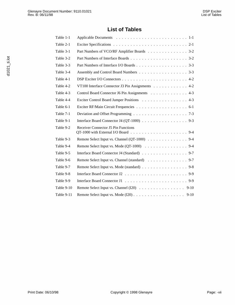
Glenayre Document Number: 9110.01021 DSP ExciterRev. B: 06/11/98 List of Tables
d102
1_ti.
lot
Print Date: 06/10/98 Copyright © 1998 Glenayre Page: -vii
List of TablesTable 1-1 Applicable Documents . . . . . . . . . . . . . . . . . . . . . . . . . 1-1
Table 2-1 Exciter Specifications . . . . . . . . . . . . . . . . . . . . . . . . . . 2-1
Table 3-1 Part Numbers of VCO/RF Amplifier Boards . . . . . . . . . . . . . . 3-2
Table 3-2 Part Numbers of Interface Boards . . . . . . . . . . . . . . . . . . . . 3-2
Table 3-3 Part Numbers of Interface I/O Boards . . . . . . . . . . . . . . . . . . 3-3
Table 3-4 Assembly and Control Board Numbers . . . . . . . . . . . . . . . . . 3-3
Table 4-1 DSP Exciter I/O Connectors . . . . . . . . . . . . . . . . . . . . . . . 4-2
Table 4-2 VT100 Interface Connector J3 Pin Assignments . . . . . . . . . . . . 4-2
Table 4-3 Control Board Connector J6 Pin Assignments . . . . . . . . . . . . . 4-3
Table 4-4 Exciter Control Board Jumper Positions . . . . . . . . . . . . . . . . 4-3
Table 6-1 Exciter RF/Main Circuit Frequencies . . . . . . . . . . . . . . . . . . 6-1
Table 7-1 Deviation and Offset Programming . . . . . . . . . . . . . . . . . . . 7-3
Table 9-1 Interface Board Connector J4 (QT-1000) . . . . . . . . . . . . . . . . 9-3
Table 9-2 Receiver Connector J5 Pin FunctionsQT-1000 with External I/O Board . . . . . . . . . . . . . . . . . . . . 9-4
Table 9-3 Remote Select Input vs. Channel (QT-1000) . . . . . . . . . . . . . . 9-4
Table 9-4 Remote Select Input vs. Mode (QT-1000) . . . . . . . . . . . . . . . 9-4
Table 9-5 Interface Board Connector J4 (Standard) . . . . . . . . . . . . . . . . 9-7
Table 9-6 Remote Select Input vs. Channel (standard) . . . . . . . . . . . . . . 9-7
Table 9-7 Remote Select Input vs. Mode (standard) . . . . . . . . . . . . . . . . 9-8
Table 9-8 Interface Board Connector J2 . . . . . . . . . . . . . . . . . . . . . . 9-9
Table 9-9 Interface Board Connector J1 . . . . . . . . . . . . . . . . . . . . . . 9-9
Table 9-10 Remote Select Input vs. Channel (I20) . . . . . . . . . . . . . . . . 9-10
Table 9-11 Remote Select Input vs. Mode (I20) . . . . . . . . . . . . . . . . . . 9-10

DSP Exciter Glenayre Document Number: 9110.01021List of Tables Rev. B: 06/11/98
Page: -viii Copyright © 1998 Glenayre Print Date: 06/10/98
Glenayre Document Number: 9110.01021 DSP ExciterRev. B: 06/11/98 GENERAL
d102
1_s1
Print Date: 06/10/98 Copyright © 1998 Glenayre Page: 1-1
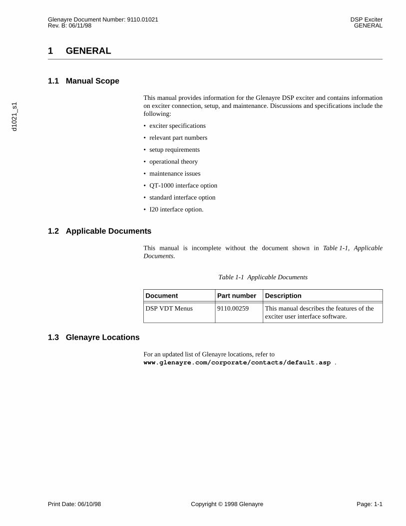
1 GENERAL
1.1 Manual Scope
This manual provides information for the Glenayre DSP exciter and contains informationon exciter connection, setup, and maintenance. Discussions and specifications include thefollowing:
• exciter specifications
• relevant part numbers
• setup requirements
• operational theory
• maintenance issues
• QT-1000 interface option
• standard interface option
• I20 interface option.
1.2 Applicable Documents
This manual is incomplete without the document shown in Table 1-1, ApplicableDocuments.
1.3 Glenayre Locations
For an updated list of Glenayre locations, refer to www.glenayre.com/corporate/contacts/default.asp .
Table 1-1 Applicable Documents
Document Part number Description
DSP VDT Menus 9110.00259 This manual describes the features of the exciter user interface software.
DSP Exciter Glenayre Document Number: 9110.01021GENERAL Rev. B: 06/11/98
Page: 1-2 Copyright © 1998 Glenayre Print Date: 06/10/98
U.S.A. CANADAGlenayre Customer Service - RF Glenayre Customer Service - RFOne Glenayre Way 1570 Kootenay StreetQuincy, Illinois 62301 USA Vancouver, BC V5K 5B8 CanadaPhone: (217) 223-3211 Phone: (604) 293-1611Fax: (217) 223-3284 Fax: (604) 293-4301
UNITED KINGDOM SINGAPOREGlenayre Electronics (UK) Ltd. Glenayre Electronics Singapore Pte. Ltd.Unit 22 Challenge House Block 5012 Ang Mo Kio Avenue 5Sherwood Drive, Bletchley TechPlace II Unit 0503Milton Keynes, MK3 6JD UK Singapore 2056Phone: 44 1 908 644 642 Phone: (65) 481-1828Fax: 44 1 908 644 643 Fax: (65) 481-2838
1.3.1 Product Warranty Information
Glenayre warrants to the original purchaser that Glenayre products are free from defects inmaterial or workmanship for a period of two years from the original invoice date, subjectto the provisions herein. Glenayre will repair or replace at its option, FOB our factory, freeof charge within one year from the date of shipment, any component, assembly or subas-sembly of our manufacture found to be defective under conditions of normal use. The unit,if repaired, will be returned to its original specifications. Failures caused by unauthorizedmodifications, force majeure, lightning, physical, environmental, or electrical damageincluding use with incompatible equipment are specifically excluded from this warranty.Glenayre disclaims any and all liability for loss or other damage whether direct, consequen-tial or of any nature whatsoever, resulting from product failure.
This warranty is in lieu of all other warranties expressed or implied and covers only thoseitems manufactured by Glenayre. Equipment supplied by, but not manufactured byGlenayre, is subject only to any warranty offered by the manufacturer of said equipment.
1.3.2 Service Warranty Information
Return of a defective item must be authorized by Glenayre prior to shipment. A ReturnAuthorization number can be obtained from Glenayre Customer Service. When requestinga Return Authorization number, give the serial number of the unit. A description of the faultshould accompany the unit on its return and the RA number must be shown on labelsattached to the item(s). The cost of shipping to Glenayre is to be paid by the customer.Shipping from Glenayre will be prepaid by the customer, and shipped via surface mail. Ifexpress shipping is required, the unit will be shipped collect.
Any repair service performed by Glenayre under this limited warranty is warranted to befree from defects in material or workmanship for ninety days from the date of repair. Allother terms of this limited warranty apply to the service warranty.
Glenayre Document Number: 9110.01021 DSP ExciterRev. B: 06/11/98 SPECIFICATIONS
d102
1_s2
Print Date: 06/10/98 Copyright © 1998 Glenayre Page: 2-1
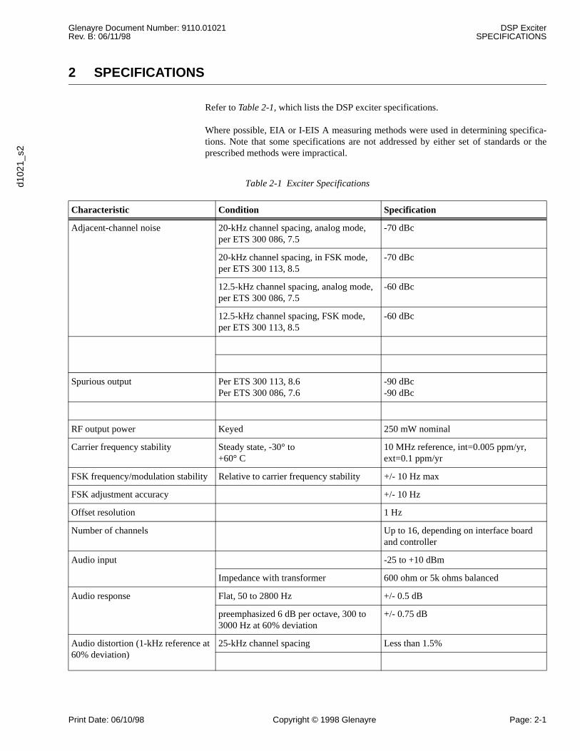
2 SPECIFICATIONS
Refer to Table 2-1, which lists the DSP exciter specifications.
Where possible, EIA or I-EIS A measuring methods were used in determining specifica-tions. Note that some specifications are not addressed by either set of standards or theprescribed methods were impractical.
Table 2-1 Exciter Specifications
Characteristic Condition Specification
Adjacent-channel noise 20-kHz channel spacing, analog mode, per ETS 300 086, 7.5
-70 dBc
20-kHz channel spacing, in FSK mode, per ETS 300 113, 8.5
-70 dBc
12.5-kHz channel spacing, analog mode, per ETS 300 086, 7.5
-60 dBc
12.5-kHz channel spacing, FSK mode, per ETS 300 113, 8.5
-60 dBc
Spurious output Per ETS 300 113, 8.6Per ETS 300 086, 7.6
-90 dBc-90 dBc
RF output power Keyed 250 mW nominal
Carrier frequency stability Steady state, -30° to +60° C
10 MHz reference, int=0.005 ppm/yr, ext=0.1 ppm/yr
FSK frequency/modulation stability Relative to carrier frequency stability +/- 10 Hz max
FSK adjustment accuracy +/- 10 Hz
Offset resolution 1 Hz
Number of channels Up to 16, depending on interface board and controller
Audio input -25 to +10 dBm
Impedance with transformer 600 ohm or 5k ohms balanced
Audio response Flat, 50 to 2800 Hz +/- 0.5 dB
preemphasized 6 dB per octave, 300 to 3000 Hz at 60% deviation
+/- 0.75 dB
Audio distortion (1-kHz reference at 60% deviation)
25-kHz channel spacing Less than 1.5%
DSP Exciter Glenayre Document Number: 9110.01021SPECIFICATIONS Rev. B: 06/11/98
Page: 2-2 Copyright © 1998 Glenayre Print Date: 06/10/98
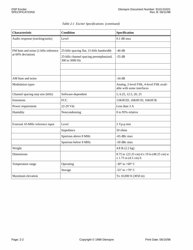
Audio response (tracking/units) Level 0.1 dB max
FM hum and noise (1-kHz reference at 60% deviation)
25-kHz spacing flat, 15-kHz bandwidth -40 dB
25-kHz channel spacing preemphasized, 300 to 3000 Hz
-55 dB
AM hum and noise -34 dB
Modulation types Analog, 2-level FSK, 4-level FSK avail-able with some interfaces
Channel spacing step size (kHz) Software-dependent 5, 6.25, 12.5, 20, 25
Emissions FCC 15K0F2D, 16K0F1D, 16K0F3E
Power requirement 22-29 Vdc Less than 3 A
Humidity Noncondensing 0 to 95% relative
External 10-MHz reference input Level 2 Vp-p min
Impedance 50 ohms
Spurious above 8 MHz -65 dBc max
Spurious below 8 MHz -50 dBc max
Weight 4.8 lb (2.2 kg)
Dimensions 8.75 in (22.25 cm) d x 19 in (48.25 cm) w x 1.75 in (4.5 cm) h
Temperature range Operating -30° to +60° C
Storage -55° to +70° C
Maximum elevation To 10,000 ft (3050 m)
Table 2-1 Exciter Specifications (continued)
Characteristic Condition Specification
Glenayre Document Number: 9110.01021 DSP ExciterRev. B: 06/11/98 DESCRIPTION
d102
1_s3
Print Date: 06/16/98 Copyright © 1998 Glenayre Page: 3-1
3 DESCRIPTION
3.1 General
The DSP exciter contains a microprocessor that allows remote or local control of the exciterand consolidates logic for varying degrees of PA control and monitoring through a videodisplay terminal (VDT). Operating characteristics of the exciter are controlled by theselection of hardware options. It is frequency-selectable by specifying the appropriateinternal frequency-determining hardware and software. It is also capable of communicatingwith several operating protocols through the proper selection of interface boards.
Refer to Table 3-1, Table 3-2, Table 3-3, and Table 3-4 for pertinent part numbers.
3.2 Physical Description
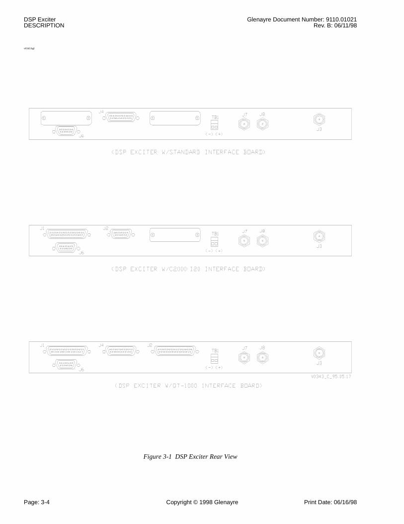
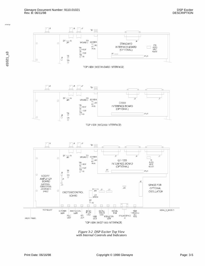
The exciter front panel contains eight LEDs, three adjustments, and one connector (also seesection 5). The exciter chassis contains three circuit boards and space for an oscillator (notused with some controllers).
Refer to Figure 3-1, which shows the exciter rear panel. The back panel contains three BNCconnectors J3/J7/J8, DB-15 connector J6, and terminal board TB1 as standard items. Otherback-panel connectors vary depending on which interface and I/O boards are installed.Figure 3-2 shows a top view of the exciter with its cover removed.
The I/O boards comprise the means to connect various controllers to the DSP exciter.
3.3 Simplified Block-Diagram Description
Refer to Figure 3-3 in the following discussion. Inputs from the transmitter controllerusually are one or two data bits, two channel-select bits, and keying input. Outputs to thecontroller are keying output indicator, various fault outputs, forward-power sample, andreflected-power sample.
DSP Exciter Glenayre Document Number: 9110.01021DESCRIPTION Rev. B: 06/11/98
Page: 3-2 Copyright © 1998 Glenayre Print Date: 06/16/98
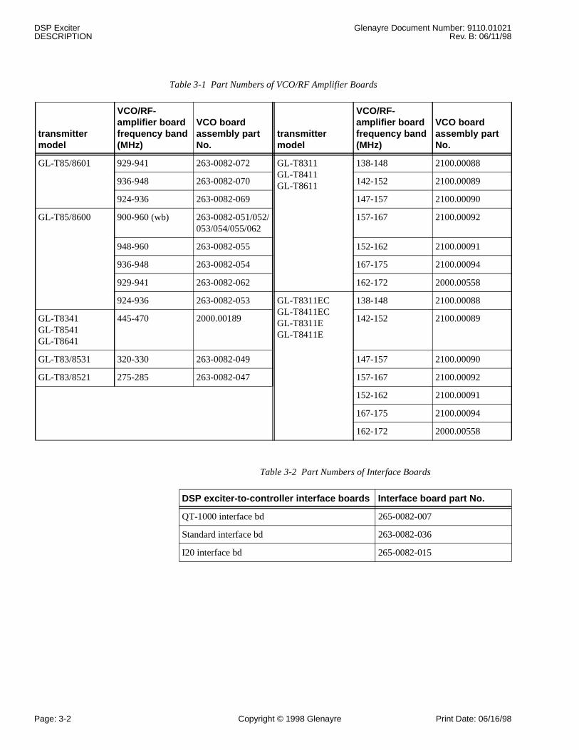
Table 3-1 Part Numbers of VCO/RF Amplifier Boards
transmitter model
VCO/RF-amplifier board frequency band (MHz)
VCO board assembly part No.
transmitter model
VCO/RF-amplifier board frequency band (MHz)
VCO board assembly part No.
GL-T85/8601 929-941 263-0082-072 GL-T8311 GL-T8411 GL-T8611
138-148 2100.00088
936-948 263-0082-070 142-152 2100.00089
924-936 263-0082-069 147-157 2100.00090
GL-T85/8600 900-960 (wb) 263-0082-051/052/053/054/055/062
157-167 2100.00092
948-960 263-0082-055 152-162 2100.00091
936-948 263-0082-054 167-175 2100.00094
929-941 263-0082-062 162-172 2000.00558
924-936 263-0082-053 GL-T8311EC GL-T8411EC GL-T8311E GL-T8411E
138-148 2100.00088
GL-T8341 GL-T8541 GL-T8641
445-470 2000.00189 142-152 2100.00089
GL-T83/8531 320-330 263-0082-049 147-157 2100.00090
GL-T83/8521 275-285 263-0082-047 157-167 2100.00092
152-162 2100.00091
167-175 2100.00094
162-172 2000.00558
Table 3-2 Part Numbers of Interface Boards
DSP exciter-to-controller interface boards Interface board part No.
QT-1000 interface bd 265-0082-007
Standard interface bd 263-0082-036
I20 interface bd 265-0082-015
Glenayre Document Number: 9110.01021 DSP ExciterRev. B: 06/11/98 DESCRIPTION
d102
1_s3
Print Date: 06/16/98 Copyright © 1998 Glenayre Page: 3-3
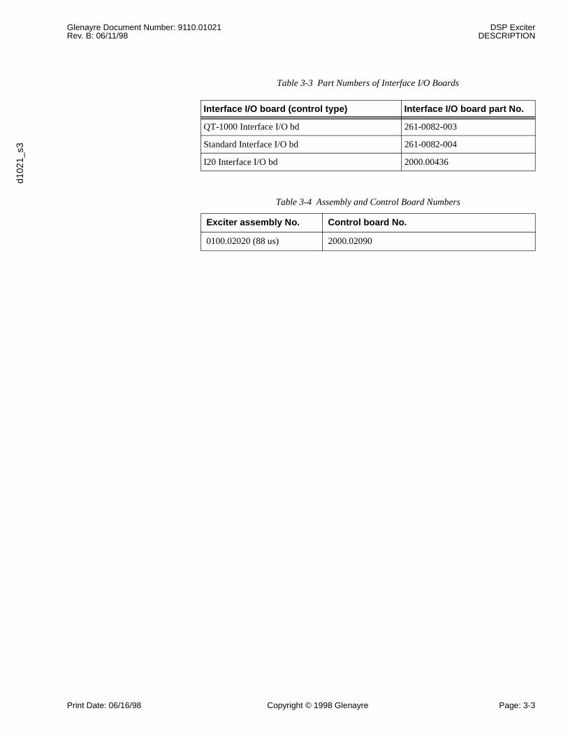
Table 3-3 Part Numbers of Interface I/O Boards
Interface I/O board (control type) Interface I/O board part No.
QT-1000 Interface I/O bd 261-0082-003
Standard Interface I/O bd 261-0082-004
I20 Interface I/O bd 2000.00436
Table 3-4 Assembly and Control Board Numbers
Exciter assembly No. Control board No.
0100.02020 (88 us) 2000.02090
DSP Exciter Glenayre Document Number: 9110.01021DESCRIPTION Rev. B: 06/11/98
Page: 3-4 Copyright © 1998 Glenayre Print Date: 06/16/98
v0343.hgl
Figure 3-1 DSP Exciter Rear View
Glenayre Document Number: 9110.01021 DSP ExciterRev. B: 06/11/98 DESCRIPTION
d102
1_s3
Print Date: 06/16/98 Copyright © 1998 Glenayre Page: 3-5
v0344.hgl
Figure 3-2 DSP Exciter Top Viewwith Internal Controls and Indicators

DSP Exciter Glenayre Document Number: 9110.01021DESCRIPTION Rev. B: 06/11/98
Page: 3-6 Copyright © 1998 Glenayre Print Date: 06/16/98
v0251.hgl
Figure 3-3 DSP Exciter Simplified Functional Diagram
Glenayre Document Number: 9110.01021 DSP ExciterRev. B: 06/11/98 INSTALLATION AND SETUP
d102
1_s4
Print Date: 06/10/98 Copyright © 1998 Glenayre Page: 4-1
4 INSTALLATION AND SETUP
4.1 Precautions and Hazards
CautionPc boards within this assembly use static-sensitivecomponents. Follow IC-handling precautions.
CautionThe exciter contains internal memory which isused to characterize exciter operation. Uponexciter replacement, ensure that replacementexciter contains appropriate items in its memory.
4.2 Test Equipment and Tools Required
Common hand tools are required for disassembly and reassembly. An RFI-immunevoltmeter may be required for voltage measurement. An in-line current meter may also benecessary for troubleshooting. A 50-ohm test load rated for 5 watts or more, an RFwattmeter rated and scaled appropriately, and RF coaxial cables are useful when verifyingRF output.
4.3 Component and Adjustment Locations
Figure 3-2, DSP Exciter Top View with Internal Controls and Indicators, shows thelocation of assemblies, internal user-adjustable controls, and I/O locations. Note: mostadjustments are performed via the front-panel VT100 interface.
4.4 Installation
4.4.1 Inspection
Inspect exciter to ensure air flow is not obstructed and cables and wires are securelyfastened to their respective connectors.
4.4.2 Power Requirement
The DSP exciter, when used as a component of a transmitter, draws its power from systemwiring. Current draw is less than three amperes at 22 to 29 volts. It is normally powered bythe transmitter power supply but can be powered by an auxiliary supply.
DSP Exciter Glenayre Document Number: 9110.01021INSTALLATION AND SETUP Rev. B: 06/11/98
Page: 4-2 Copyright © 1998 Glenayre Print Date: 06/10/98
4.4.3 Input/Output Connections
Figure 3-1 shows the locations of I/O connectors; Table 4-1 lists I/O connectors anddescribes their functions. Normally the exciter is delivered as part of an entire transmitterand has already been installed in a rack, with all connections already made, except forconnections to equipment that was not installed in the rack before shipment. If I/O connec-tions are required, refer to the system-interconnect diagram and other instructions in thetransmitter manual.
4.4.4 Signal Functions
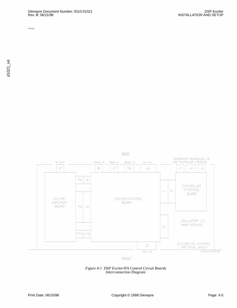
See Table 4-1, which references other tables that describe pin-by-pin functions of multipinconnectors, for details. Figure 4-1 shows interconnections among internal assemblies.
Table 4-1 DSP Exciter I/O Connectors
Stencil/Connector DescriptionAdditional Detail
VT100 INTERFACE: J3 VT100 interface to VDT (front) Table 4-2
RF OUT: J3 RF out, on frequency Figure 6-1
QT-1000 interface I/O J4 Interface to QT-1000 interface board Table 9-1
QT-1000 interface I/O J5 DB-9 connector, to receiver Table 9-2
Standard interface I/O J4 Interface to standard interface I/O board Table 9-1
I20 (C2000) interface I/O J2 Interface to C2000 interface I/O board Table 9-8
I20 (C2000) interface I/O J1 Interface to C2000 interface I/O board Table 9-9
PA CONTROL: J6 Connects to PA Table 4-3
ISOLATOR IN: J7 VSWR input from PA Figure 3-1
10 MHZ IN: J8 External reference input from interface Figure 3-1
+26 VDC: TB1 Exciter input power, +22-29 Vdc Figure 3-1
Table 4-2 VT100 Interface Connector J3 Pin Assignments
J3-X (front) Signal Description
2 TXD Transmit data line
3 RXD Receive data line
5 GND Ground
1,4,6,7,8,9 Not used
Glenayre Document Number: 9110.01021 DSP ExciterRev. B: 06/11/98 INSTALLATION AND SETUP
d102
1_s4
Print Date: 06/10/98 Copyright © 1998 Glenayre Page: 4-3
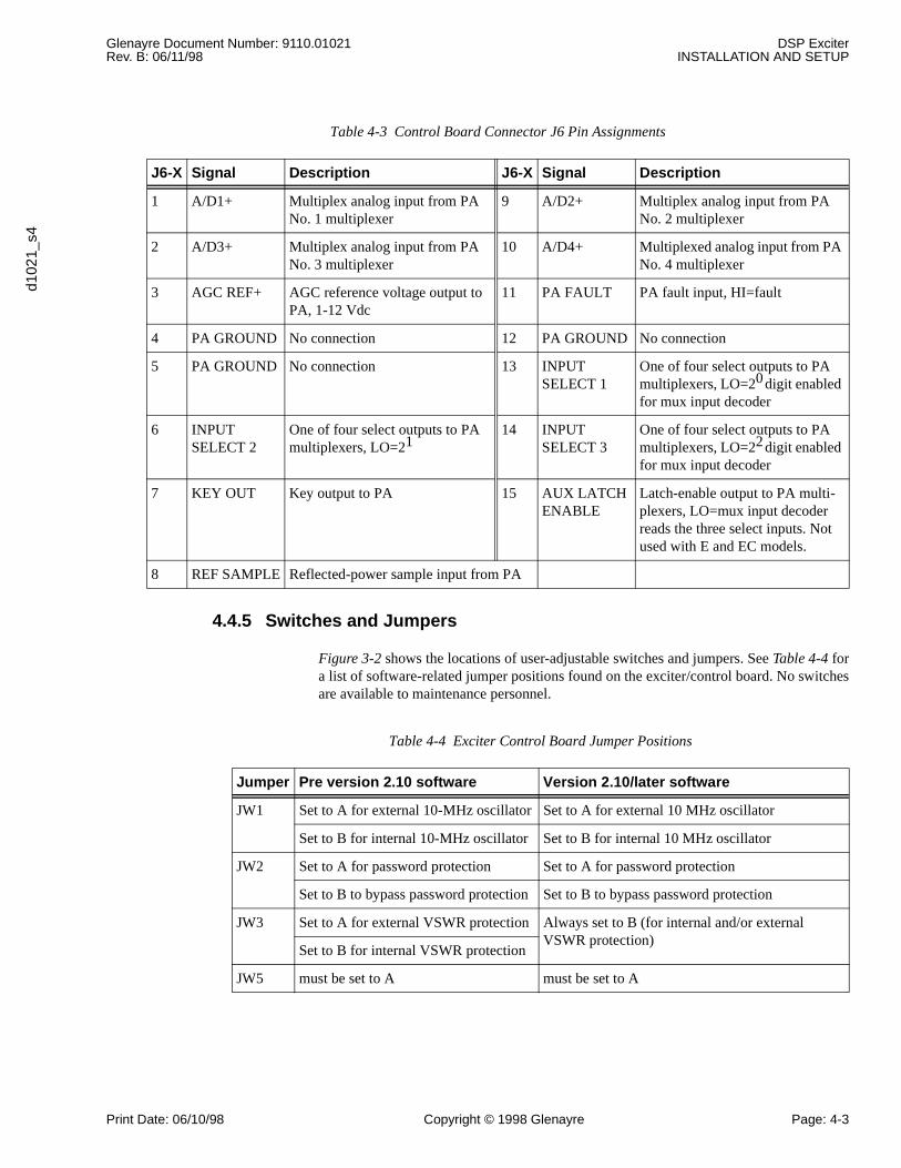
4.4.5 Switches and Jumpers
Figure 3-2 shows the locations of user-adjustable switches and jumpers. See Table 4-4 fora list of software-related jumper positions found on the exciter/control board. No switchesare available to maintenance personnel.
Table 4-3 Control Board Connector J6 Pin Assignments
J6-X Signal Description J6-X Signal Description
1 A/D1+ Multiplex analog input from PA No. 1 multiplexer
9 A/D2+ Multiplex analog input from PA No. 2 multiplexer
2 A/D3+ Multiplex analog input from PA No. 3 multiplexer
10 A/D4+ Multiplexed analog input from PA No. 4 multiplexer
3 AGC REF+ AGC reference voltage output to PA, 1-12 Vdc
11 PA FAULT PA fault input, HI=fault
4 PA GROUND No connection 12 PA GROUND No connection
5 PA GROUND No connection 13 INPUT SELECT 1
One of four select outputs to PA multiplexers, LO=20 digit enabled for mux input decoder
6 INPUT SELECT 2
One of four select outputs to PA multiplexers, LO=21
14 INPUT SELECT 3
One of four select outputs to PA multiplexers, LO=22 digit enabled for mux input decoder
7 KEY OUT Key output to PA 15 AUX LATCH ENABLE
Latch-enable output to PA multi-plexers, LO=mux input decoder reads the three select inputs. Not used with E and EC models.
8 REF SAMPLE Reflected-power sample input from PA
Table 4-4 Exciter Control Board Jumper Positions
Jumper Pre version 2.10 software Version 2.10/later software
JW1 Set to A for external 10-MHz oscillator Set to A for external 10 MHz oscillator
Set to B for internal 10-MHz oscillator Set to B for internal 10 MHz oscillator
JW2 Set to A for password protection Set to A for password protection
Set to B to bypass password protection Set to B to bypass password protection
JW3 Set to A for external VSWR protection Always set to B (for internal and/or external VSWR protection)
Set to B for internal VSWR protection
JW5 must be set to A must be set to A
DSP Exciter Glenayre Document Number: 9110.01021INSTALLATION AND SETUP Rev. B: 06/11/98
Page: 4-4 Copyright © 1998 Glenayre Print Date: 06/10/98
4.5 Setup
NoteWhen doing a setup for a wideband DSP exciter, the net channel changetime must be set for 300 ms.
Refer to the DSP exciter VDT menus and user manual for transmitter-control setup infor-mation. All setup is done via the front-panel VT100 interface.
4.6 Ultimate Disposition
CautionThis equipment may contain hazardous materials.Check with the local EPA or other environmentalauthority before disposing of this equipment.
4.7 Grounding
As viewed from the back, the exciter chassis has a ground stud on the right side of the rearpanel. It is shipped from the factory properly connected to ground with a green or green-with-yellow-stripe wire. In newer cabinets, the chassis ground wire is connected to agrounding bus inside the cabinet. The ground bus is connected to a ground stud on theinterface plate mounted to the top of the cabinet.
CautionImproper, inadequate, or faulty grounding cancause erratic equipment operation. Theseconditions can also perpetuate equipment failure.
Glenayre Document Number: 9110.01021 DSP ExciterRev. B: 06/11/98 INSTALLATION AND SETUP
d102
1_s4
Print Date: 06/10/98 Copyright © 1998 Glenayre Page: 4-5
v0164.hgl
Figure 4-1 DSP Exciter/PA Control Circuit Boards Interconnection Diagram
DSP Exciter Glenayre Document Number: 9110.01021INSTALLATION AND SETUP Rev. B: 06/11/98
Page: 4-6 Copyright © 1998 Glenayre Print Date: 06/10/98
Glenayre Document Number: 9110.01021 DSP ExciterRev. B: 06/11/98 OPERATION
d102
1_s5
Print Date: 06/16/98 Copyright © 1998 Glenayre Page: 5-1
5 OPERATION
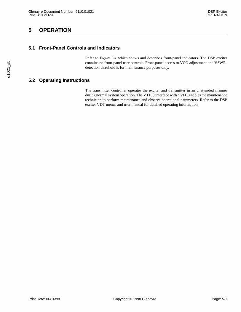
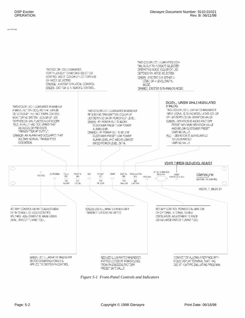
5.1 Front-Panel Controls and Indicators
Refer to Figure 5-1 which shows and describes front-panel indicators. The DSP excitercontains no front-panel user controls. Front-panel access to VCO adjustment and VSWR-detection threshold is for maintenance purposes only.
5.2 Operating Instructions
The transmitter controller operates the exciter and transmitter in an unattended mannerduring normal system operation. The VT100 interface with a VDT enables the maintenancetechnician to perform maintenance and observe operational parameters. Refer to the DSPexciter VDT menus and user manual for detailed operating information.
DSP Exciter Glenayre Document Number: 9110.01021OPERATION Rev. B: 06/11/98
Page: 5-2 Copyright © 1998 Glenayre Print Date: 06/16/98
mod.v0079.hgl
Figure 5-1 Front-Panel Controls and Indicators
VSWRTHRESHOLD ADJ
',*,7$/��*5((1�:+,/(�02'8/$7('$1$/2*�
96:5�7+5(6+2/'�/(9(/�$'-867
Glenayre Document Number: 9110.01021 DSP ExciterRev. B: 06/11/98 THEORY OF OPERATION
d102
1_s6
Print Date: 06/16/98 Copyright © 1998 Glenayre Page: 6-1
6 THEORY OF OPERATION
6.1 Exciter/PA Control
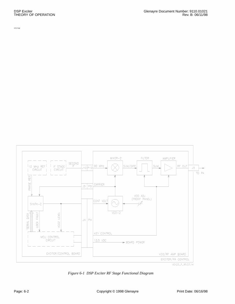
Refer to Figure 6-1, which describes signal flow in the DSP exciter with the transmittercontroller interface. The following major paragraphs describe the operation of the majoritems within the figure. Additional detailed figures are referenced, as required.
6.1.1 Reference Source
The 10-MHz reference signal is provided by the transmitter controller via J8 on the exciter/control board or by an optional internal reference oscillator. All other inputs and outputs,except for RF output, are routed through the interface board.
6.1.2 Main Circuit Frequencies
The VCO/RF amplifier board installed determines the frequency for the RF output.Table 6-1 lists VCO/RF amplifier board frequencies and the corresponding exciter/outputfrequencies.
6.1.3 Controller Interface Functions
The exciter interfaces with the transmitter controller through the exciter interface I/Oboard. Alarm signals, consisting of transmitter alarm, fault, and status signals, are supplieddirectly to the transmitter controller. See Paragraph 9, OPTIONS, for details.
6.2 Interface to Controller
Refer to Section 9, OPTIONS, for details.
Table 6-1 Exciter RF/Main Circuit Frequencies
Exciter Output Frequency (MHz)
First IF Frequency (kHz)
Second IF Frequency (MHz)
VCO-1 Frequency (MHz)
VCO-2 Frequency (MHz)
900-960 100 90 89.9 810-870
445-470 100 90 89.9 535-560
275-330 100 90 89.9 365-420
130-180 100 90 89.9 220-270
DSP Exciter Glenayre Document Number: 9110.01021THEORY OF OPERATION Rev. B: 06/11/98
Page: 6-2 Copyright © 1998 Glenayre Print Date: 06/16/98
v0123.hgl
Figure 6-1 DSP Exciter RF Stage Functional Diagram
Glenayre Document Number: 9110.01021 DSP ExciterRev. B: 06/11/98 THEORY OF OPERATION
d102
1_s6
Print Date: 06/16/98 Copyright © 1998 Glenayre Page: 6-3
6.3 DSP Modulator
6.3.1 General
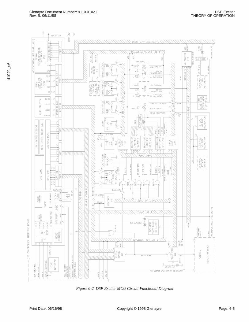
The DSP modulator circuit converts the data into the first IF signal, which is fully modu-lated. The IF stage circuit converts the first IF signal into the second IF signal. The RF stagecircuit converts the second IF signal into the RF output. Ten MHz is used as frequencyreference by each conversion stage. The DSP modulator is the portion of exciter circuitrybetween the controller interface and the IF stage. The DSP modulator uses digital signalprocessing to modulate and up-convert the paging information into the first IF signal. Themodulation type depends on the transmitter operating mode. The IF stage is the portion ofexciter circuitry between the DSP modulator and the RF stage. The IF stage uses hetero-dyne mixing to generate the optimum second IF signal frequency, which depends on therequirement of the VCO/RF amplifier board installed. The MCU control circuit is thecommand and control hub of the transmitter. The type of control software depends on thetransmitter frequency and power output. The following text describes main exciter circuitrythat works for all software programs, modulation schemes, and IF signal frequencies.Figure 6-2 shows additional details.
6.3.2 DSP Modulator Signal Flow
Refer to Figure 6-2 in the following discussion. The inputs that provide the paging infor-mation to the DSP modulator circuit are digitized audio and FSK data, supplied by thecontroller interface circuit through connector pair P1/J1. Digitized audio arrives as serialdata. FSK data arrives as parallel data. The DSP modulator circuit processes the digitizedaudio in the analog mode or the FSK data in the digital mode. The result of this processingis the exciter’s first IF signal, which is applied to the IF stage circuit. To produce the firstIF signal, the DSP modulator contains two DSPs (a signal modulator and a quadraturemodulator), a digital-to-analog converter, and a read-only memory. The following textdescribes these four components and their signal flow.
6.3.2.1 Digital Signal Modulator
The signal modulator (SM) generates modulation that contains the paging information,which is supplied by digitized audio or FSK data. The digitized audio is input into a serialinput port. An external edge detector is required to input the FSK data. The SM convertsone of the data inputs into a modulated signal, which is mathematically represented withinthe SM as a vector signal, defined by its rectangular coordinates. These coordinates,commonly known as I and Q, are supplied to the digital quadrature modulator as 16-bitparallel data. The modulated signal output from the SM depends on the following signalcharacteristics:
• modulation scheme
• frequency response or rise time
• input logic or data inversion
• deviation level or bandwidth
• offset from carrier frequency
• analog gain and deviation limit.
DSP Exciter Glenayre Document Number: 9110.01021THEORY OF OPERATION Rev. B: 06/11/98
Page: 6-4 Copyright © 1998 Glenayre Print Date: 06/16/98
The SM also performs all communications between the DSP modulator circuit and theMCU control circuit. These communications are through the SM 16-bit parallel data port.External input and output latches expand the capabilities of this port. Control inputs consistof commands such as reset, request status, set paging signal parameter, change mode, andboot program. Requested status outputs consist of current mode, deviation levels, inputlevel, input gain, modulation detected, and current polarity. Nonrequested status outputsindicate the existence of analog limiting and modulation.
6.3.2.2 Digital Quadrature Modulator
The digital quadrature modulator (DQM) does interpolation and up-conversion of themodulated signal. Modulated signal input to the DQM is applied by the SM as I and Qcomponents (16-bit parallel). The DQM performs trigonometric computations at a muchhigher sampling rate, which determines first-IF signal value and frequency. The modulatedsignal output from the DQM is supplied from its serial data port to the D/A converter.
6.3.2.3 Digital-to-Analog Converter
The digital input to the digital-to-analog (D/A) converter is the modulated signal from theDQM. This data arrives as serial data. The analog output from the D/A converter is the firstIF signal. In addition to the IF stage circuit, the first IF signal is supplied to the MCUcontrol circuit, where it is rectified and filtered to generate fault logic.
6.3.2.4 Read-Only Memory
A programmable and erasable read-only memory (PEROM) stores the modulator programsfor both DSPs. These programs are transferred to the SM when the exciter is booted(powered up), then the SM transfers the program to the DQM. The nonvolatile PEROMretains its program for years. Its memory may be individually reprogrammed withouterasing the entire chip.
6.4 IF Stage
Refer to Figure 6-1. The input to the IF stage is the first IF signal, which is supplied by theDSP modulator circuit. The first IF signal carries all the paging information on an interme-diate carrier frequency. The IF stage performs direct up-conversion of the first IF signal tocreate the second IF signal, which carries the same paging information as the first IF signal,but on a higher carrier frequency. The second IF signal is applied to the RF stage throughconnector pair J10/P10. To produce the second IF signal, the IF stage contains mixer-1 andfilter circuits. Supporting these circuits are VCO-1 and synthesizer-1 circuits. Figure 6-2and Figure 6-3 show additional details.
6.4.1 Filter-1
This is an active filter circuit that acts as an anti-aliasing filter. It provides at least 20 dB ofrejection at the sampling image frequency (300 kHz). Output of this filter goes to mixer-1.
Glenayre Document Number: 9110.01021 DSP ExciterRev. B: 06/11/98 THEORY OF OPERATION
d102
1_s6
Print Date: 06/16/98 Copyright © 1998 Glenayre Page: 6-5
Figure 6-2 DSP Exciter MCU Circuit Functional Diagram
DSP Exciter Glenayre Document Number: 9110.01021THEORY OF OPERATION Rev. B: 06/11/98
Page: 6-6 Copyright © 1998 Glenayre Print Date: 06/16/98
6.4.2 Mixer-1
Mixer-1 is the first heterodyne mixer. Inputs to mixer-1 are a modulated IF and a carrier.The modulated IF input is the first IF signal. The carrier input is supplied by VCO-1. Theoutput from mixer-1 consists of two modulated carriers that are sums and differencefrequencies of the inputs. These two frequencies are applied to the filter circuit.
6.4.3 Filter-2
The filter is centered at the second IF signal frequency with an 18-kHz bandwidth. Theinput to the filter consists of two modulated carriers. These are sum and difference frequen-cies supplied by mixer-1. Output from the filter is only the sum frequency. This modulatedoutput is the second IF signal.
6.4.4 VCO-1
VCO-1 is the local oscillator for the IF stage. The input to VCO-1 is a dc control voltage.This voltage controls VCO-1 carrier frequency and is supplied by synthesizer-1. The outputfrom VCO-1 is a sine-wave carrier and is applied to mixer-1.
6.4.5 Synthesizer-1
Synthesizer-1 controls VCO-1 carrier frequency by means of a phase-locked loop (PLL).PLL inputs are a carrier and a phase reference. The reference input is a 10-MHz carriersupplied by the 10-MHz reference circuit. The carrier input is from VCO-1. The PLLoutput is a dc control voltage. This voltage, set to cause the VCO-1 carrier to lock phasewith the reference, is supplied to VCO-1.
Synthesizer-1 also performs all communications between the IF stage circuit and the MCUcontrol circuit. A control input specifies the VCO-1 carrier frequency; this data is receivedover a serial data link when the exciter is booting or changing channels. Status outputs area lock fault and a VCO1 level. The lock fault indicates loss of the carrier/reference phaselock. The VCO1 level is the VCO-1 control voltage.
6.5 MCU
Refer to Figure 6-4. Control outputs are supplied by the MCU control circuit to the otherfunctional circuits. Likewise, status inputs are applied to the MCU control circuit from theother functional circuits. Discussions of these control and status signals are included withthe information on the other major functional circuits. To interface these control and statussignals, the MCU control circuit contains an MCU, D/A converter, 8/16 bit converter, read-only memory, and a VSWR-fault detector. To light the front-panel LEDs, the MCU controlcircuit contains a bank of PNP switching transistors. Refer to Figure 6-2 and the followingtext which describes this circuitry and its signal flow.
Glenayre Document Number: 9110.01021 DSP ExciterRev. B: 06/11/98 THEORY OF OPERATION
d102
1_s6
Print Date: 06/16/98 Copyright © 1998 Glenayre Page: 6-7
6.5.1 Microcontroller Unit (MCU)
The MCU contains a central processing unit (CPU), memories, peripherals, and otherhardware on a single chip. The primary internal functions of the MCU and their applicationin the exciter are described in the following list.
• An eight-bit remote input port accepts discrete low power mode, keyline, and channelselects from the controller interface circuit. An external edge detector is required to inputthe channel selects.
• Interrupt logic stops or reduces RF transmission when a fault input is received, e.g. aVSWR or PA fault.
• An on-board oscillator/clock generator, driven by an external crystal, times internalMCU functions. A synchronized clock output times external functions.
• The MCU performs most interfacing through a parallel communications link: eight-bitdata bus, sixteen-bit address bus, and a read/write line. External input and output latchesexpand the capability of this link.
• An eight-bit input/output port supplies discrete keyline, RF status, and chip selectcontrols to the exciter and the PA.
• A serial peripheral interface (SPI) supplies synchronous serial frequency data to the IFstage and RF stage circuits. Individual commands load the program into either IF stage’ssynthesizer-1 or RF stage synthesizer-2.
• An eight-input analog-to-digital (A/D) converter measures voltage inputs from theexciter and the PA. External multiplexers expand MCU analog inputs up to 41.
• A serial communications interface (SCI) exchanges asynchronous serial RS-232 datawith the VT100 VDT. An external RS-232 driver buffers the MCU data, allowing it tobe exchanged through external connector J3.
• A random-access memory (RAM) temporarily stores transmitter fault and alarm values.
• An electrically-erasable read-only memory (EEPROM) permanently stores transmittersignal parameters.
6.5.2 Digital-to-Analog (D/A) Converter
A D/A converter generates an AGC reference voltage. The D/A converter inputs are dataand select logic. The data, supplied by the MCU when the D/A is selected, represents thedesired transmitter power output. The D/A converter output is an AGC reference voltage.This voltage represents a level proportional to the desired transmitter power output. TheAGC reference voltage, output via J6, is used by the PA to generate an AGC voltage.
6.5.3 8/16-Bit Converter
An 8/16-bit converter allows the MCU eight-bit data bus to communicate with the 16-bitdata bus of the DSP modulator circuit. The MCU must perform two read or write proce-dures, a low byte and a high byte, to each one of the DSP modulator circuits. The converterprovides two status outputs to the MCU and DSP modulator. A data-available-to-MCUstatus indicates that the DSP modulator circuit has written data into the converter that theMCU must read. A data-available-to-DSP status indicates that the MCU has written datainto the converter that the DSP modulator circuit must read. If that DSP modulator circuitdoes not read data that the MCU has written, a DSP communication fault is generated.
DSP Exciter Glenayre Document Number: 9110.01021THEORY OF OPERATION Rev. B: 06/11/98
Page: 6-8 Copyright © 1998 Glenayre Print Date: 06/16/98
6.5.4 Read-Only Memory
A programmable and erasable read-only memory (PEROM) stores the control program forthe transmitter. This program is transferred to the MCU when the exciter is booted up. Thenonvolatile PEROM retains its program for years. Its memory may be individually repro-grammed without erasing the entire chip.
6.5.5 VSWR-Fault Detector
The exciter receives a VSWR signal from the PA through connector J6. This signal is arectified dc voltage sample generated by the isolator. The voltage sample is monitored bythe MCU to provide the value for the total reflected-power indication. The voltage sampleis also monitored by a fault circuit in the exciter. If a factory-preset voltage is exceeded, thefault circuit shuts down the transmitter or reduces power by an interrupt to the MCU.
6.5.6 Alarm Data-to-Logic Conversion
The transmitter controller reads logic alarm inputs; most are stored as data in the MCUcontrol circuit. If the controller interface converts the data to individual logic signals for thecontroller, data from MCU control representing the alarms is clocked into a pair of latches.The latches convert the data into continuous logic signals. These signals and others controla bank of NPN switching transistors that supply the actual logic signal to the controller.Control logic gates convert chip controls from the MCU into a clock input for the latches.
6.5.7 Alarm Data-to-Logic Conversion
The transmitter controller reads logic alarm inputs; most are stored as data in the MCUcontrol circuit. If the controller interface converts the data to individual logic signals for thecontroller, data from MCU control representing the alarms is clocked into a pair of latches.The latches convert the data into continuous logic signals. These signals and others controla bank of NPN switching transistors that supply the actual logic signal to the controller.Control logic gates convert chip controls from the MCU into a clock input for the latches.
Glenayre Document Number: 9110.01021 DSP ExciterRev. B: 06/11/98 THEORY OF OPERATION
d102
1_s6
Print Date: 06/16/98 Copyright © 1998 Glenayre Page: 6-9
DSP Exciter Glenayre Document Number: 9110.01021THEORY OF OPERATION Rev. B: 06/11/98
Page: 6-10 Copyright © 1998 Glenayre Print Date: 06/16/98
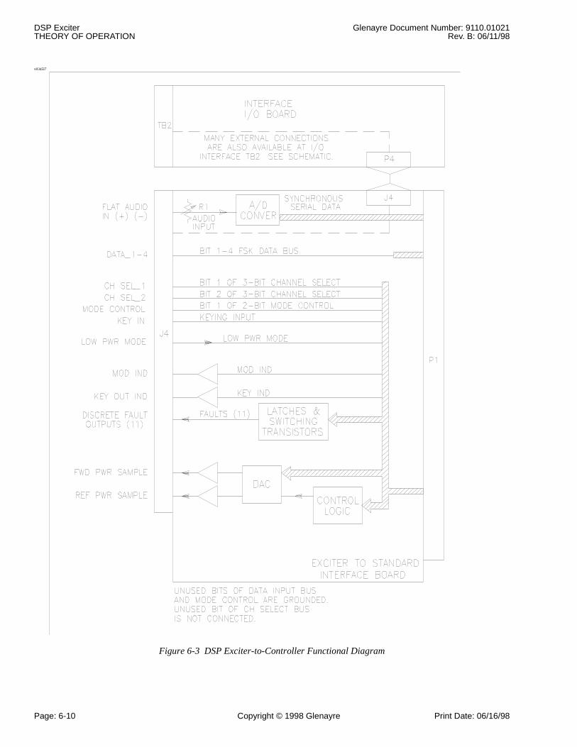
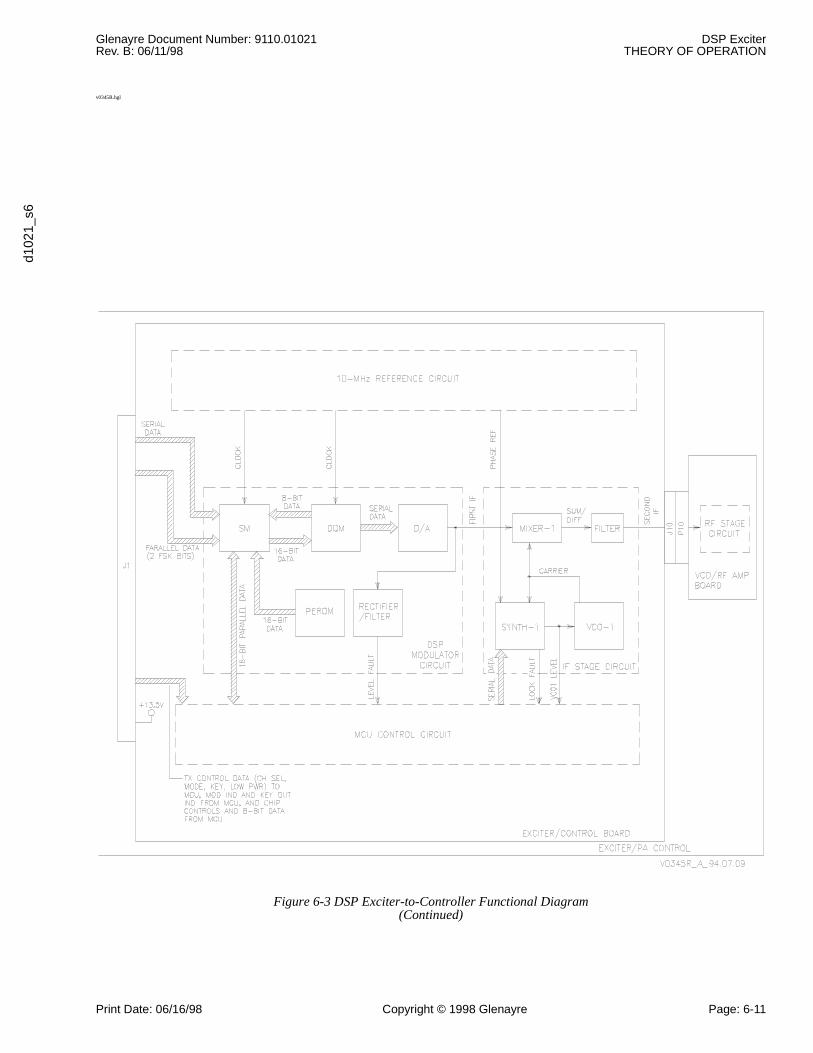
v0345l7
Figure 6-3 DSP Exciter-to-Controller Functional Diagram
Glenayre Document Number: 9110.01021 DSP ExciterRev. B: 06/11/98 THEORY OF OPERATION
d102
1_s6
Print Date: 06/16/98 Copyright © 1998 Glenayre Page: 6-11
v0345R.hgl
Figure 6-3 DSP Exciter-to-Controller Functional Diagram(Continued)
DSP Exciter Glenayre Document Number: 9110.01021THEORY OF OPERATION Rev. B: 06/11/98
Page: 6-12 Copyright © 1998 Glenayre Print Date: 06/16/98
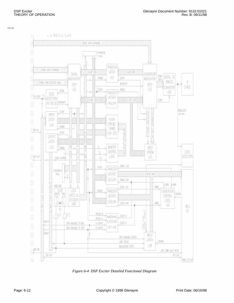
v0081.hgll
Figure 6-4 DSP Exciter Detailed Functional Diagram
Glenayre Document Number: 9110.01021 DSP ExciterRev. B: 06/11/98 THEORY OF OPERATION
d102
1_s6
Print Date: 06/16/98 Copyright © 1998 Glenayre Page: 6-13
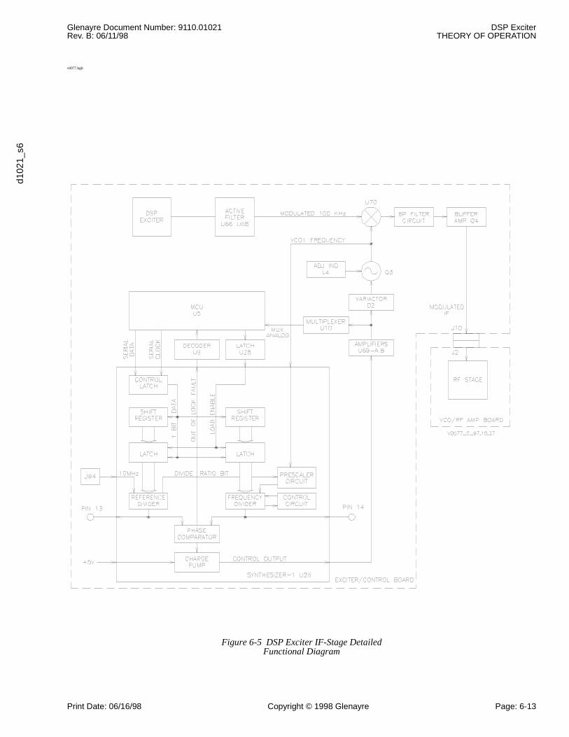
v0077.hglr
Figure 6-5 DSP Exciter IF-Stage DetailedFunctional Diagram
DSP Exciter Glenayre Document Number: 9110.01021THEORY OF OPERATION Rev. B: 06/11/98
Page: 6-14 Copyright © 1998 Glenayre Print Date: 06/16/98
6.6 RF Assemblies
6.6.1 RF Stage Location
The RF stage circuits are located on two circuit boards, both housed within the exciterchassis. The exciter/control board is the main circuit board and the VCO/RF amplifierboard is a selected option. The exciter/control board connects to the VCO/RF amplifierboard through three connector pairs: J4/P4, J9/P9, and J10/P10. The VCO/RF amplifierboard also contains BNC connector J3, which extends through the rear panel of the exciter.This board contains most of the RF stage components inside an RF shield. A hole in theshield and the front panel provide access to an RF stage adjustment, which is marked VCOADJ on the front panel.
6.6.2 RF Assemblies
6.6.2.1 RF Stage Description
The RF stage is the portion of exciter circuitry between the IF stage and RF out and is thefinal major functional circuit. The RF stage determines transmitter RF output frequencyand the highest and lowest possible RF output frequencies (RF band). The transmitter canbe operated at several RF bands, depending on the RF stage circuitry installed in the exciter.
6.6.2.2 RF Stage Bands
The selected VCO/RF amplifier board determines the RF band of the transmitter.
6.6.2.3 RF Stage Signal Flow
Refer to Figure 6-1. Input to the RF stage is the second IF signal, supplied by the IF stagecircuit through connector pair J10/P10. The second IF signal carries paging information ona modulated carrier at the exciter’s second intermediate frequency. The RF stage convertsthe second IF signal into the exciter’s RF output. This RF output carries the same paginginformation as the second IF signal, but on a modulated carrier of radio frequency. The RFoutput is normally applied to the PA through connector J3. To produce the RF output, theRF stage contains mixer-2, filters, and an amplifier. Supporting these circuits are VCO-2and synth-2. The following text describes these five circuits and their signal flow.
6.6.2.3.1 Mixer-2
Mixer-2 is the second heterodyne mixer. Inputs to mixer-2 are a modulated IF and a carrier.The modulated IF is the second IF signal. The carrier is supplied by VCO-2. Output frommixer-2 consists of sum and difference frequencies of the inputs. The sum frequency iscentered near the channel carrier, and the difference frequency about twice the second IFfrequency below that. These two modulated RF carriers are applied to the filter circuit.
Glenayre Document Number: 9110.01021 DSP ExciterRev. B: 06/11/98 THEORY OF OPERATION
d102
1_s6
Print Date: 06/16/98 Copyright © 1998 Glenayre Page: 6-15
6.6.2.3.2 Filter
The filter is factory-selected and tuned, with a bandwidth determined by carrier frequencyof the transmitter. The inputs to the filter consist of two modulated RF carriers and a keycontrol.The two carriers are sum and difference frequencies, supplied by mixer-2. The keycontrol is supplied by the MCU control circuit through J4/P4. The output from the filter,supplied when the key control is received, is only the sum frequency. This modulated RF,centered near the channel on-frequency, is supplied to the amplifier.
6.6.2.3.3 Amplifier
The amplifier provides amplification to the value listed in the specifications as exciter RFpower out. The inputs to the amplifier consist of modulated RF and a key control. Themodulated RF, mixer-2 sum output frequency, is supplied through the filter. Key control issupplied by the MCU control circuit through J4/P4. Output from the amplifier, suppliedwhen the key control is received, is an amplified version of the modulated RF. Thisamplified output is the exciter RF output.
6.6.2.3.4 VCO-2
VCO-2 is the RF stage local oscillator. Inputs to VCO-2 are a dc control voltage and anadjustment. Dc control voltage is supplied by synthesizer-2. The adjustment, which variesthe VCO2 control voltage level, is controlled through the front-panel VCO ADJ access.This control provides the means for VCO-2 to output a carrier frequency that wouldotherwise be beyond the range of the control voltage input. The carrier output, alwayssecond IF frequency below the channel carrier frequency, is applied to mixer-2.
6.6.2.3.5 Synthesizer-2
Synthesizer-2 controls VCO-2 carrier frequency by means of a phase-locked loop (PLL).PLL inputs to synthesizer-2 are a carrier and a phase reference. The reference is a 10-MHzcarrier supplied by the 10-MHz reference circuit. The carrier is the VCO-2 output. The PLLoutput from synthesizer-2 is a dc control voltage. This voltage, set to cause VCO-2 to lockphases with the reference, is applied to the VCO-2 control input.
Synthesizer-2 also performs all communications between the RF stage circuit and the MCUcontrol circuit. A control input to synthesizer-2 specifies VCO-2 carrier frequency. Thisdata is received over a serial data link when the exciter is booting or changing channels.Status outputs from synthesizer-2 are a lock fault and a VCO2 level. The lock fault indicatesloss of the carrier/reference phase lock. VCO2 level is the VCO-2 control voltage.
6.7 Voltage Regulator Circuit
Refer to Figure 6-4 for pertinent information in the following discussion. The exciterreceives 26-volt operating power through terminal board TB1on the rear of the chassis. Thedc power indicator on the exciter front panel is connected to this input. This voltage issupplied to a 26-volt bus and is monitored by the MCU. An intermediate regulator reducesthe 26 volts to 16.5 volts, which is supplied to the two final regulators. One regulatorgenerates 13.5 volts, which is supplied to a 13.5-volt bus and monitored by the MCU. Theother regulator generates 5 volts, which is supplied to a 5-volt bus and monitored by theMCU.

DSP Exciter Glenayre Document Number: 9110.01021THEORY OF OPERATION Rev. B: 06/11/98
Page: 6-16 Copyright © 1998 Glenayre Print Date: 06/16/98
Glenayre Document Number: 9110.01021 DSP ExciterRev. B: 06/11/98 MAINTENANCE
d102
1_s7
Print Date: 06/16/98 Copyright © 1998 Glenayre Page: 7-1
7 MAINTENANCE
7.1 Location of Maintenance Procedures
The DSP exciter is central to performing transmitter maintenance. Most maintenance ofelectrical assemblies is done via the VT100 interface. Any maintenance procedures whichrequire adjusting controls within the exciter chassis are listed in this section.
Replace the exciter if it has input power, as indicated by the front-panel DC POWER LED,but does not allow the user to make connection via the VT100 interface.
7.2 Test Equipment Required
See Paragraph 4.2, Test Equipment and Tools Required, for a list test equipment requiredto perform maintenance procedures.
7.3 VCO-2 Adjustment Procedure
Perform the VCO-2 adjustment procedure after installing new VCO/RF amplifier board orafter setting new channel carrier frequency. If the transmitter is to operate at more than onefrequency, perform the multichannel adjustment procedure. If the transmitter is to operateat only one frequency, perform the single-channel adjustment procedure. Refer to the DSPexciter VDT manual as necessary.
7.3.1 VCO-2 Multichannel Adjustment Procedure
1. Set up VT100 VDT and select local control (see VDT manual).
2. Select transmitter channel of lowest frequency if not already selected.
3. Use tuning tool supplied to adjust VCO ADJ control through exciter front panel. Ad-just for a reading of 3.3 to 3.5 volts on VCO2 status display.
4. Return transmitter to service.
Procedure is complete.
7.3.2 VCO-2 Single-Channel Adjustment Procedure
This procedure does not apply to wideband option.
1. Set up VT100 VDT and select local control (see VDT manual).
2. Select transmitter channel of operating frequency if not already selected.
3. Use tuning tool supplied to adjust VCO ADJ control through exciter front panel. Ad-just for reading of 5.0 Vdc on VCO2 status display.
4. Return transmitter to service.
Procedure is complete.
DSP Exciter Glenayre Document Number: 9110.01021MAINTENANCE Rev. B: 06/11/98
Page: 7-2 Copyright © 1998 Glenayre Print Date: 06/16/98
7.4 Over-The-Link Downloading
Over-the-link (OTL) code downloading allows GL-C2000 transmitter controller(GL-C2000) software, alarm matrix setup, and exciter software to be downloaded over theGL-C2000 link channel.
To properly use OTL downloading, GL-C2000 units must be programmed for the correctcontrol group, site ID, and unit ID, which are integral to GL-C2000 hardware and software.When information is downloaded over the link channel, the control group, site IDs and/orunit IDs that are to receive the code must be specified.
CautionIf the control group, site ID, and unit ID are notspecified, all units in the system accept thedownload information. In a mixed system, this canresult in some of the transmitters being off the air.An example of this would be a GL-T8600 exciterreceiving a GL-T8500 exciter programming code.The GL-T8600 exciter would not operate with thissoftware and could result in a site visit to correctthe problem.
Programming of control groups and site IDs is done via the GL-C2000 front port with alocal connection or through a modem from a remote location. The control groups should besetup as a group of transmitters having the same configuration. For example, all GL-T8500transmitters could be in one control group and GL-T8600 transmitters be in another. Thiswould allow one to download exciter software to all GL-T8500 transmitters at one time byselecting their control group. Any transmitter with a different control group would notaccept the download information.
Site ID must be different for each site location, and is used when downloading informationto a specific site location. If there are multiple units at the same site, the site ID and unit IDneed to be specified to download to a specific unit. If the unit ID is not specified, all unitsat that site accept the download.
Unit ID is programmed with a rotary switch in the GL-C2000; it must be different for eachGL-C2000 at a site location. To download one specific unit, both site and unit ID must bespecified for that unit; the unit with that site ID and unit ID is the only one that accepts thedownload.
NoteFor assistance on software downloading, call Glenayre CustomerSupport at 800-637-9181 or 217-223-3211.
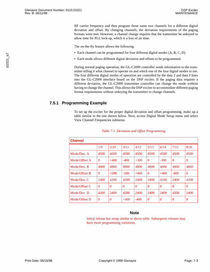
7.5 On-The-Fly Channel/Mode Changing
Different paging formats may require different digital deviation and offsets of paging dataon the same RF carrier frequency. In the past, the only way to meet the different deviationrequirements on the same frequency was to program two different channels for the same
Glenayre Document Number: 9110.01021 DSP ExciterRev. B: 06/11/98 MAINTENANCE
d102
1_s7
Print Date: 06/16/98 Copyright © 1998 Glenayre Page: 7-3
RF carrier frequency and then program those same two channels for a different digitaldeviation and offset. By changing channels, the deviation requirements of the pagingformats were met. However, a channel change requires that the transmitter be unkeyed toallow time for PLL lock-up, which is a loss of air time.
The on-the-fly feature allows the following.
• Each channel can be programmed for four different digital modes (A, B, C, D).
• Each mode allows different digital deviation and offsets to be programmed.
During normal paging operation, the GL-C2000 controller sends information to the trans-mitter telling it what channel to operate on and which one of the four digital modes to use.The four different digital modes of operation are controlled by the data 2 and data 3 linesinto the GL-C2000 interface board on the DSP exciter. If the paging data requires adifferent deviation, the GL-C2000 transmitter controller can change the mode withouthaving to change the channel. This allows the DSP exciter to accommodate different pagingformat requirements without unkeying the transmitter to change channels.
7.5.1 Programming Example
To set up the exciter for the proper digital deviation and offset programming, make up atable similar to the one shown below. Next, access Digital Mode Setup menu and selectView Channel Frequencies submenu.
NoteInitial release has setup similar to above table. Subsequent releases mayhave more programming variations.
Table 7-1 Deviation and Offset Programming
Channel
1/9 2/10 3/11 4/12 5/13 6/14 7/15 8/16
Mode/Dev. A 4500 4500 4500 4500 4500 4500 4500 4500
Mode/Offset A 0 +400 -400 +300 0 -300 0 0
Mode/Dev. B 4800 4800 4800 4800 4800 4800 4800 4800
Mode/Offset B 0 +200 -200 +400 0 +400 -400 0
Mode/Dev. C 2400 4200 4200 2400 2400 4200 2400 4200
Mode/Offset C 0 0 0 0 0 0 0 0
Mode/Dev. D 4200 2400 4200 2400 2400 2400 4200 2400
Mode/Offset D 0 0 +400 -400 0 0 0 0
DSP Exciter Glenayre Document Number: 9110.01021MAINTENANCE Rev. B: 06/11/98
Page: 7-4 Copyright © 1998 Glenayre Print Date: 06/16/98
NoteWhen on-the-fly software is used with a QT-1000 interface boardinstalled in the exciter, only the deviation and offset programming formode D is available. References in the exciter menus pertaining to modesA, B, and C are blanked out.
7.5.1.1 DSP Exciter (2.1) / GL-C2000 (2.3)
The GL-C2000 detects a FLEX baud rate of 1600. When this condition is detected, themode control lines to the DSP exciter change it to mode B. If the FLEX baud rate is notdetected, the mode control lines are set for mode A. This requires that mode A deviation(and offset) be set for POCSAG (512, 1200 or 2400 baud), Golay, NEC or any other pagingformat other than FLEX requirements. Mode B deviation and offset must be set for FLEX.Mode C is used in later releases.
7.5.1.2 DSP Exciter (3.0) / GL-C2000 (3.0) / GL3000 (6.0)
This software/hardware combination makes all four modes accessible on the fly (OTF).Refer to the latest GL-C2000 manual for OTF mode configuration.
7.6 16-Channel Operation
With 16-channel capability, the on-the-fly digital mode programming is only program-mable on 8 channels. When channels 1 through 8 are programmed for different modes,channels 9 through 16 follow the same mode programming respectively (i.e. channel 9 isthe same as 1, channel 10 is the same as 2, etc.). Selecting additional channels (9 through16) is achieved by the GL-C2000 controller pulling mode-1 line low to the GL-C2000interface board.
These parameters: Fwd Pwr alarm, Low Pwr alarm, Deviation, Offset, andFiltering are mapped from channels 1 through 8 to channels 9 through 16, respectively.The center frequency is uniquely programmable for all 16 channels. The GL-C2000 onlyaccesses channels 9 through 16 if it is configured for serial frequency-control mode.
Glenayre Document Number: 9110.01021 DSP ExciterRev. B: 06/11/98 MAINTENANCE
d102
1_s7
Print Date: 06/16/98 Copyright © 1998 Glenayre Page: 7-5
7.7 On-The-Fly Interface
Figure 7-1 On-The-Fly GL-C2000 Control Lines to DSP Exciter
DSP Exciter Glenayre Document Number: 9110.01021MAINTENANCE Rev. B: 06/11/98
Page: 7-6 Copyright © 1998 Glenayre Print Date: 06/16/98
Notes:
A GL-C2000 interface board must be installed in the DSP exciter whenever on-the-flysoftware is installed.
All J1 pin connections shown in Figure 7-1 are at the input to the GL-C2000 interfaceboard in the DSP exciter.
Data 0 at the input of the GL-C2000 interface board controls Data 1 at its output.Data 1 at the input of the GL-C2000 interface board controls Data 2 at its output.Data 2 at the input of the GL-C2000 interface board controls Data 3 at its output.Data 3 at the input of the GL-C2000 interface board controls Data 4 at its output.
Mode 0 at the input of the GL-C2000 interface board controls Mode Sel 1 at its output.Mode 1 at the input of the GL-C2000 interface board controls Ch Sel 4 at its output.
Freq 0 at the input of the GL-C2000 interface board controls Ch Select 1 at its output.Freq 1 at the input of the GL-C2000 interface board controls Ch Select 2 at its output.Freq 2 at the input of the GL-C2000 interface board controls Ch Select 3 at its output.
7.8 Checkout
The DSP exciter has two functions; it produces on-frequency RF and has a microprocessorto handle input from the PA and transmitter controller. Checkout involves verifying that RFis produced and unkeying occurs during a fault condition.
7.9 Troubleshooting
The recommended troubleshooting level for the exciter is at the unit level. That is, if theexciter fails to provide the transmitter system with a usable, modulated RF-drive signal andall the exciter’s power, control, and signal inputs are normal, replace the exciter with aspare. Determine that the spare is compatible in hardware (VCO and RF amplifier) andsoftware/firmware. Some parameters must be programmed into a replacement exciter forsystem compatibility.
Glenayre Document Number: 9110.01021 DSP ExciterRev. B: 06/11/98 REMOVAL AND REINSTALLATION
d102
1_s8
Print Date: 06/10/98 Copyright © 1998 Glenayre Page: 8-1
8 REMOVAL AND REINSTALLATION
Remove all input power from the transmitter cabinet before performing these procedures.
8.1 Exciter/PA Control Chassis
See Figure 8-1 for a detailed drawing.
NoteMemory PROMs in the replacement exciter should be the same as in theoriginal exciter unless the maintenance technician intends to modifyexciter characteristics. Also, parameters such as channel frequencies,may be stored in nonvolatile RAM. Ensure that the replacement exciteris programmed correctly.
8.1.1 Removal Procedure
1. Support exciter while removing the four screws from the front panel that secure it to the cabinet. Save screws for installation procedure.
2. Remove exciter from cabinet far enough to access back panel.
3. Disconnect connector J3 from connector P3 that is pigtailed off terminal board TB1 (dc power input).
4. If a controller interface I/O panel is mounted on exciter back panel, remove I/O panel; leave all wires connected to I/O panel.
5. Tag all connectors attached to the exciter back panel.
6. Remove all connectors attached to the exciter back panel. Leave P3 connector/wiring assembly connected to terminal board TB1 for now.
7. Remove exciter and tag wires connected to terminal board TB1 on P3 connector/wir-ing assembly.
8. Disconnect tagged wires from terminal board TB1. Save P3 connector/wiring assem-bly for installation procedure.
Procedure is complete.
8.1.2 Reinstallation Procedure
NoteA wideband DSP exciter that is installed in a GL-T8500 or GL-T8600transmitter must have one rack unit of space between it and the poweramplifier chassis.
1. Before installing exciter, connect wires on P3 connector/wiring assembly (from re-moval procedure) to terminal board TB1 on exciter back panel.
2. Connect connectors on transmitter to exciter back panel.
DSP Exciter Glenayre Document Number: 9110.01021REMOVAL AND REINSTALLATION Rev. B: 06/11/98
Page: 8-2 Copyright © 1998 Glenayre Print Date: 06/10/98
3. If controller requires interface I/O board, install external interface I/O board on excit-er back panel (see Paragraph 8.4).
4. Connect connector J3 to connector P3 that is pigtailed off of terminal board TB1.
5. Locate connector P3 that is pigtailed off of terminal board TB1. Disconnect connector P3 from connector J3.
6. Slide exciter into cabinet and secure with four screws saved from removal procedure.
Procedure is complete. Perform setup, adjustment, or calibration procedures as required.
8.2 Exciter Cover
These procedures must be performed with the exciter removed from the transmitter cabinet.Refer to Figure 8-2 throughout these procedures.
8.2.1 Removal Procedure
1. Remove two sem screws from sides of exciter cover. Save sem screws for installation procedure.
2. Raise front of cover and extract back of cover from channel in back panel extrusion.
3. Remove exciter cover.
Procedure is complete.
8.2.2 Reinstallation Procedure
1. Insert exciter cover into channel on exciter back panel extrusion.
2. Lower cover so that fingerstock is behind exciter front panel.
3. While pressing down slightly on exciter cover: install two sem screws saved from re-moval procedure through sides of exciter cover.
Procedure is complete.
Glenayre Document Number: 9110.01021 DSP ExciterRev. B: 06/11/98 REMOVAL AND REINSTALLATION
d102
1_s8
Print Date: 06/10/98 Copyright © 1998 Glenayre Page: 8-3
v0151.hgl
Figure 8-1 DSP Exciter Chassis Removal and Reinstallation
DSP Exciter Glenayre Document Number: 9110.01021REMOVAL AND REINSTALLATION Rev. B: 06/11/98
Page: 8-4 Copyright © 1998 Glenayre Print Date: 06/10/98
v0171.hgl
Figure 8-2 DSP Exciter Cover Removal and Reinstallation
Glenayre Document Number: 9110.01021 DSP ExciterRev. B: 06/11/98 REMOVAL AND REINSTALLATION
d102
1_s8
Print Date: 06/10/98 Copyright © 1998 Glenayre Page: 8-5
8.3 Exciter/Control Board
These procedures must be performed with the exciter removed from the transmitter cabinet,and the exciter cover removed. Refer to Figure 8-3 throughout these procedures.
8.3.1 Removal Procedure
NoteSave all hardware for reinstallation procedure.
1. Remove controller interface board (see Paragraph 8.4 ).
2. Remove VCO/RF amplifier board (see Paragraph 8.5 ).
3. Remove three kep nuts and three screws from regulators U1, U2, and U58.
4. Remove shoulder washer from regulator U58.
5. Remove two jam nuts and two lock washers from connectors J7 and J8.
6. Remove two jack socket screws attached to connector J6 through back panel.
7. Remove four sem screws from back panel and remove back panel from exciter chas-sis. Some exciters use three sem screws and one standoff.
8. Remove insulator between back panel and regulator U58.
9. Remove two jack socket screws attached to connector J3 through front panel.
10. Remove two studded standoffs through exciter/control board.
11. Remove nine sem screws that attach exciter/control board to exciter chassis, and re-move exciter/control board.
Procedure is complete.
8.3.2 Reinstallation Procedure
NoteUse hardware saved from installation procedure.
CautionBe careful to not overtighten hardware.
1. Position exciter/control board onto exciter chassis and secure with nine sem screws.
2. Install two studded standoffs through exciter/control board.
3. Apply Vibra Tite or similar nonpermanent self-locking liquid adhesive to threads of the two jack socket screws to be used for connector J3. Apply only to top 1/4 inch of thread on each jack socket screw.
4. Install two jack-socket screws into connector J3 through front panel.
DSP Exciter Glenayre Document Number: 9110.01021REMOVAL AND REINSTALLATION Rev. B: 06/11/98
Page: 8-6 Copyright © 1998 Glenayre Print Date: 06/10/98
5. Apply thermal compound as follows: between regulator U1 and back panel, between regulator U2 and back panel, between regulator U58 and insulator, and between insu-lator and back panel.
6. Install insulator between regulator U58 and back panel.
7. Position back panel on exciter chassis and secure with four sem screws. Some excit-ers use three sem screws and one standoff in the bottom right corner.
8. Apply Vibra Tite or similar nonpermanent self-locking liquid adhesive to threads of the two jack socket screws to be used for connector J6. Apply only to top 1/4 inch of thread on each jack-socket screw.
9. Install two jack socket screws into connector J6 through back panel.
10. Install two lock washers and two jam nuts over connectors J7 and J8.
11. Install shoulder washer into regulator U58.
12. Install three kep nuts and three screws through regulators U1, U2, and U58.
13. Install VCO/RF amplifier board (see Paragraph 8.5 ).
14. Install controller interface I/O board (see Paragraph 8.4).
Procedure is complete. After exciter is installed in transmitter cabinet, perform setupprocedure if necessary (refer to the system and menu manuals).
Glenayre Document Number: 9110.01021 DSP ExciterRev. B: 06/11/98 REMOVAL AND REINSTALLATION
d102
1_s8
Print Date: 06/10/98 Copyright © 1998 Glenayre Page: 8-7
v0170.hgl
Figure 8-3 DSP Exciter Control Board Removal and Reinstallation
DSP Exciter Glenayre Document Number: 9110.01021REMOVAL AND REINSTALLATION Rev. B: 06/11/98
Page: 8-8 Copyright © 1998 Glenayre Print Date: 06/10/98
8.4 Interface I/O Board
These procedures must be performed with the exciter removed from the transmitter cabinet(see Paragraph 8.1), and the exciter cover removed (see Paragraph 8.2). Refer to Figure 8-4 throughout the following procedures.
8.4.1 Removal Procedure
1. Remove jack socket screws (2 or 6) securing connector J4 (J1 and J2 not always used) to the rear panel of the exciter. Save jack socket screws for installation procedure.
2. Remove two sem screws securing interface board to standoffs. Save sem screws for installation procedure.
3. Grasp interface board at the center of connector P1. Pull up on board with a firm ver-tical motion to disengage connector P1 from connector J1 on the exciter/control board.
4. Remove interface board.
Procedure is complete.
8.4.2 Reinstallation Procedure
1. Position interface board into place by inserting connector J4 (and J1 and J2 if used) through openings in exciter rear panel.
2. Carefully align connector P1 on interface board with connector J1 on exciter/control board and engage.
3. Secure interface board to standoffs with two sem screws saved from removal proce-dure.
4. Apply Vibra Tite or similar nonpermanent self-locking liquid adhesive to threads of the six jack socket screws saved from removal procedure. Apply only to top 1/4 inch of thread on each jack socket screw.
5. Screw the six jack socket screws through holes on exciter rear panel at either sides of connectors J1, J4, and J2.
Procedure is complete. After exciter is installed into transmitter cabinet, perform audioinput adjustment procedure (see DSP VDT Menus manual, PN 9110.00259).
Glenayre Document Number: 9110.01021 DSP ExciterRev. B: 06/11/98 REMOVAL AND REINSTALLATION
d102
1_s8
Print Date: 06/10/98 Copyright © 1998 Glenayre Page: 8-9
8.5 VCO/RF Amplifier Board
These procedures must be performed with the exciter removed from the transmitter cabinet(see Paragraph 8.1), and the exciter cover removed (see Paragraph 8.2). Refer to Figure 8-5 throughout these procedures.
8.5.1 Removal Procedure
1. Remove jam nut and lock washer from connector J3 on rear of exciter. Save jam nut and lock washer for installation procedure.
2. Remove five sem screws securing VCO/RF amplifier board to standoffs on exciter. Save sem screws for installation procedure.
3. Grasp VCO/RF amplifier board near connector P4. Pull up on board with a short ver-tical motion to disengage connectors P4/P9/P10 from connectors J4/J9/J10 on exciter/control board.
4. Remove VCO/RF amplifier board.
Procedure is complete.
8.5.2 Reinstallation Procedure
1. Before installing VCO/RF amplifier board, verify that RF band includes desired transmitter operating frequencies.
2. Position VCO/RF amplifier board into place by inserting connector J3 through hole in rear of exciter.
3. Carefully align connectors P4/P9/P10 on VCO/RF amplifier board with connectors J4/J9/J10 on exciter/control board and engage.
4. Secure VCO/RF amplifier board to standoffs on exciter using five sem screws saved from removal procedure.
5. Install lockwasher and jam nut to connector J3 on rear of exciter using lockwasher and jam nut saved from removal procedure.
Procedure is complete. After exciter is installed into transmitter cabinet, perform VCO2adjustment procedure. See Paragraph 7.3 for details.
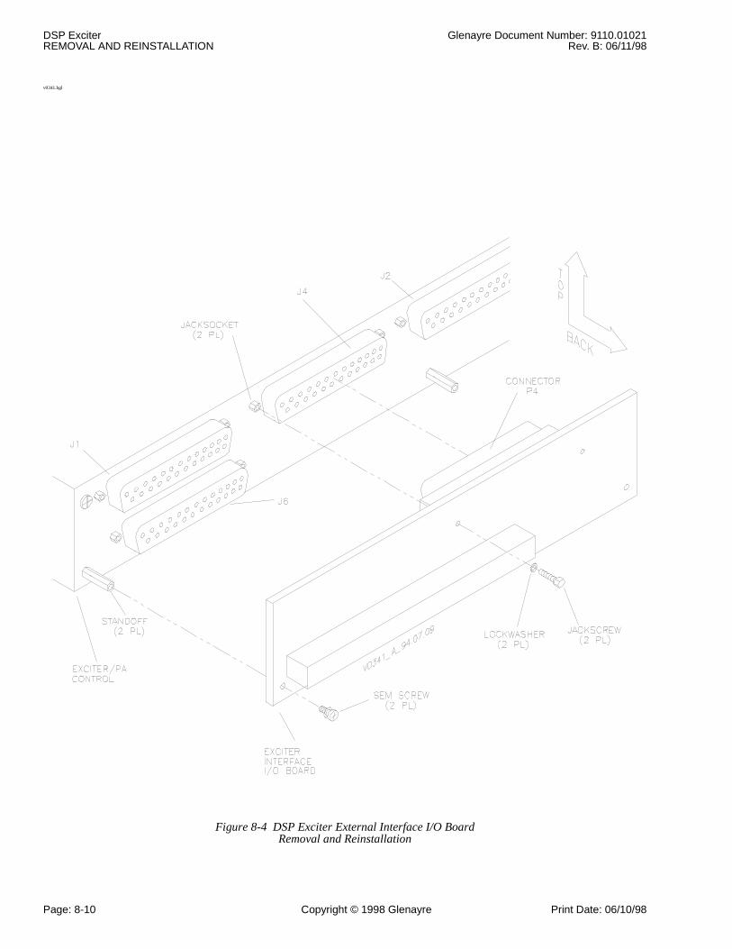
DSP Exciter Glenayre Document Number: 9110.01021REMOVAL AND REINSTALLATION Rev. B: 06/11/98
Page: 8-10 Copyright © 1998 Glenayre Print Date: 06/10/98
v0341.hgl
Figure 8-4 DSP Exciter External Interface I/O BoardRemoval and Reinstallation
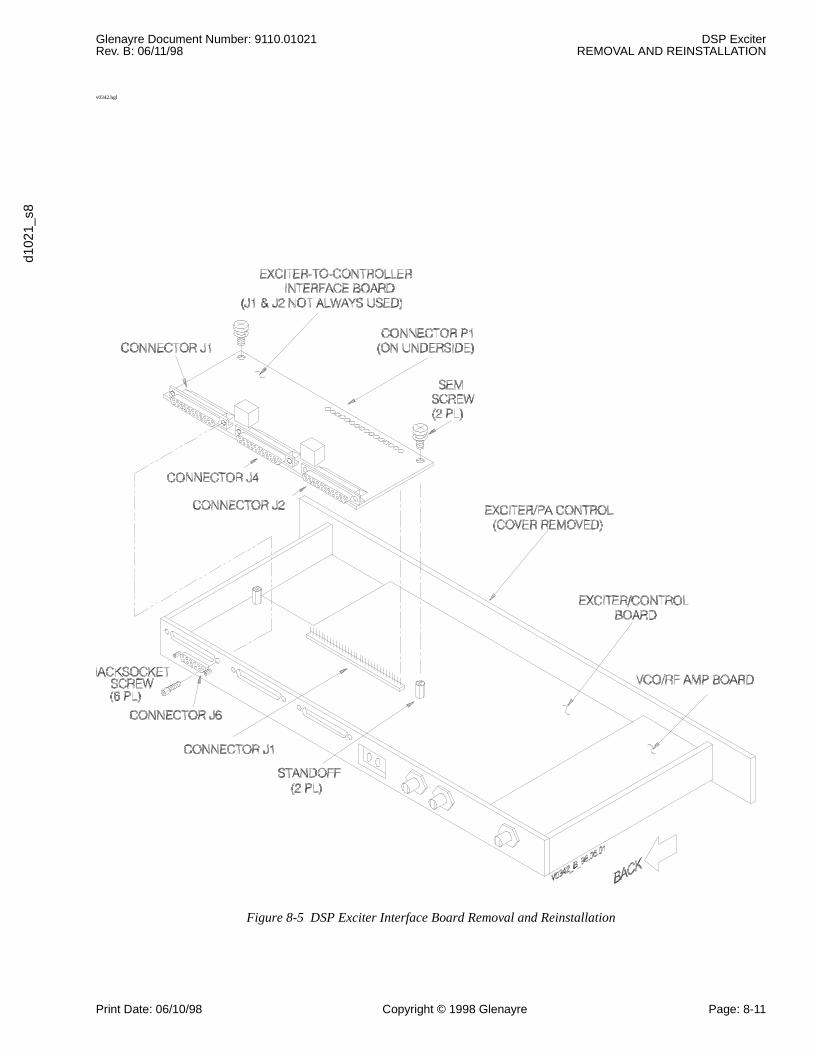
Glenayre Document Number: 9110.01021 DSP ExciterRev. B: 06/11/98 REMOVAL AND REINSTALLATION
d102
1_s8
Print Date: 06/10/98 Copyright © 1998 Glenayre Page: 8-11
v0342.hgl
Figure 8-5 DSP Exciter Interface Board Removal and Reinstallation

DSP Exciter Glenayre Document Number: 9110.01021REMOVAL AND REINSTALLATION Rev. B: 06/11/98
Page: 8-12 Copyright © 1998 Glenayre Print Date: 06/10/98
Glenayre Document Number: 9110.01021 DSP ExciterRev. B: 06/11/98 OPTIONS
d102
1_s9
Print Date: 06/16/98 Copyright © 1998 Glenayre Page: 9-1
9 OPTIONS
9.1 Exciter/PA Control w/ QT-1000 Interface
The controller interface is the portion of exciter circuitry that connects the transmittercontroller to the exciter. The controller interface dictates what kind of transmitter controllermay operate the transmitter. The transmitter can be operated through one of several control-lers depending on the interface circuitry installed with the exciter. Two boards comprise thisinterface: the internal QT-1000 interface board and the external interface I/O board.
Control commands from the transmitter controller are connected through the interfacecircuit. This circuit supplies remote control to the microcontroller unit (MCU) controlcircuit. The VT100 VDT supplies local control. The MCU control circuit generates allcontrol signals for the other circuits, and monitors their status. The MCU control circuitreports status back to the VT100 VDT and the interface circuit, which supplies the statusto the transmitter controller.
9.1.1 Reference Source
A 10-MHz reference signal is provided by the controller via J8 on the exciter/control board.
9.1.2 Controller Interface Connector Functions (QT-1000)
Refer to Table 9-1, and Table 9-2 for a pin-by-pin description of signal functions. Thecontroller interfaces with the transmitter through connectors J1, J2, and J5 and terminalboard TB2 at the exciter back panel. J5 on the external I/O board connects to a standardRL-xx3 receiver, if installed. If a standard receiver is not installed, TB2 on the external I/O board connects to any generic receiver. TB2 also makes connections to optional config-urable QT-1000 alarm inputs and switching outputs. J1 on the internal interface boardconnects directly to TXC connector J1, and interfaces all signals except alarms. Alarmsignals, consisting of transmitter alarm, fault, and status signals, are supplied directly to theQT-1000 controller connector J2 on the internal interface board.
9.1.3 Interface Conversion Functions (QT-1000)
Some signals exchanged between the controller and exciter originate with a format,voltage, or requirement incompatible with their destination. The QT-1000 interfaceperforms signal conversions necessary to provide compatibility between the controller andexciter. The following describes any signal conversions made by the controller interface.
9.1.3.1 Analog-Mode A/D Conversion
The exciter DSP modulator circuit reads synchronized serial data for its analog mode inputsignal, but the QT-1000 controller provides an analog signal. The controller interfaceconverts the analog to appropriate data form for the DSP. The analog (FLAT AUDIO+,-)terminates across a balanced input circuit that also provides a level adjustment. The adjust-ment, when properly set by the AUDIO INPUT ADJUST pot through the exciter cover,provides analog to an A/D converter at the optimum 0-dBm level. The A/D converts analog
DSP Exciter Glenayre Document Number: 9110.01021OPTIONS Rev. B: 06/11/98
Page: 9-2 Copyright © 1998 Glenayre Print Date: 06/16/98
into serial data, which is applied to the DSP through a synchronous data link. A synchro-nous data link is characterized by exchange of pulse streams for timing purposes. The A/Dconverter is clocked by a pulse generator circuit driven by the 10-MHz reference circuit.
9.1.3.2 FSK-Data-Bit Strapping
The exciter DSP modulator circuit reads two bits (DATA 1,2) from the QT-1000 for itsdigital FSK mode input signal. This allows transmitter operation in the four-level mode.Data bits 3 and 4 are unavailable with the QT-1000 interface (internally grounded).
9.1.3.3 Channel-Select-Bit Strapping
The exciter MCU reads two bits (CH SELECT 1,2) from the QT-1000 to determine theremotely-selected channel. As a result, the QT-1000 can command only four channels. TheQT-1000 interface keeps bit 3 open (high). Refer to Table 9-6 for transmitter operatingchannel resulting from the channel select inputs.
9.1.3.4 Mode-Select-Bit Strapping
The exciter MCU reads one bit (MODE SELECT 1) from the QT-1000 to determine theremotely-selected mode. Refer to Table 9-7 for the transmitter operating mode resultingfrom the mode select input.
9.1.3.5 Power Sample D/A Conversion
The QT-1000 reads two 0-to-2.5-volt voltages for its forward and reflected power sampleinputs, but these power values are stored as data in the exciter MCU control circuit. TheQT-1000 interface converts data to voltages of the appropriate range for the QT-1000. Datafrom the MCU representing the forward and reflected powers is written into a dual D/Aconverter. The D/A converts data into two proportional dc voltages ranging from 0 volt to2.5 volts (FWD PWR SAMPLE, REF PWR SAMPLE), which are applied to the QT-1000.Control logic gates ensure that data is written to the proper half of the D/A converter.
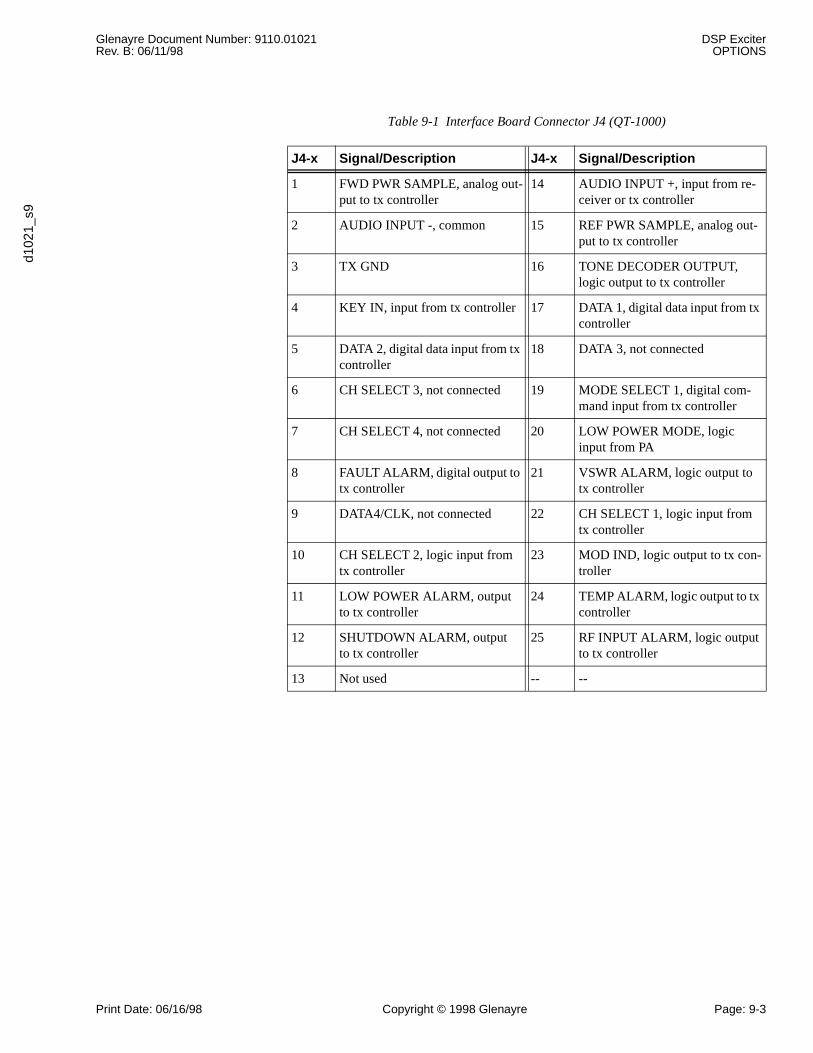
Glenayre Document Number: 9110.01021 DSP ExciterRev. B: 06/11/98 OPTIONS
d102
1_s9
Print Date: 06/16/98 Copyright © 1998 Glenayre Page: 9-3
Table 9-1 Interface Board Connector J4 (QT-1000)
J4-x Signal/Description J4-x Signal/Description
1 FWD PWR SAMPLE, analog out-put to tx controller
14 AUDIO INPUT +, input from re-ceiver or tx controller
2 AUDIO INPUT -, common 15 REF PWR SAMPLE, analog out-put to tx controller
3 TX GND 16 TONE DECODER OUTPUT, logic output to tx controller
4 KEY IN, input from tx controller 17 DATA 1, digital data input from tx controller
5 DATA 2, digital data input from tx controller
18 DATA 3, not connected
6 CH SELECT 3, not connected 19 MODE SELECT 1, digital com-mand input from tx controller
7 CH SELECT 4, not connected 20 LOW POWER MODE, logic input from PA
8 FAULT ALARM, digital output to tx controller
21 VSWR ALARM, logic output to tx controller
9 DATA4/CLK, not connected 22 CH SELECT 1, logic input from tx controller
10 CH SELECT 2, logic input from tx controller
23 MOD IND, logic output to tx con-troller
11 LOW POWER ALARM, output to tx controller
24 TEMP ALARM, logic output to tx controller
12 SHUTDOWN ALARM, output to tx controller
25 RF INPUT ALARM, logic output to tx controller
13 Not used -- --
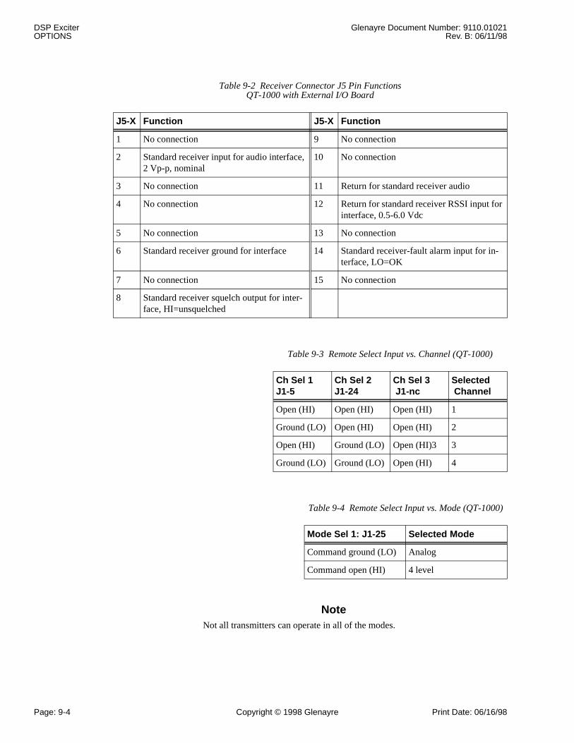
DSP Exciter Glenayre Document Number: 9110.01021OPTIONS Rev. B: 06/11/98
Page: 9-4 Copyright © 1998 Glenayre Print Date: 06/16/98
NoteNot all transmitters can operate in all of the modes.
Table 9-2 Receiver Connector J5 Pin FunctionsQT-1000 with External I/O Board
J5-X Function J5-X Function
1 No connection 9 No connection
2 Standard receiver input for audio interface, 2 Vp-p, nominal
10 No connection
3 No connection 11 Return for standard receiver audio
4 No connection 12 Return for standard receiver RSSI input for interface, 0.5-6.0 Vdc
5 No connection 13 No connection
6 Standard receiver ground for interface 14 Standard receiver-fault alarm input for in-terface, LO=OK
7 No connection 15 No connection
8 Standard receiver squelch output for inter-face, HI=unsquelched
Table 9-3 Remote Select Input vs. Channel (QT-1000)
Ch Sel 1 J1-5
Ch Sel 2J1-24
Ch Sel 3 J1-nc
Selected Channel
Open (HI) Open (HI) Open (HI) 1
Ground (LO) Open (HI) Open (HI) 2
Open (HI) Ground (LO) Open (HI)3 3
Ground (LO) Ground (LO) Open (HI) 4
Table 9-4 Remote Select Input vs. Mode (QT-1000)
Mode Sel 1: J1-25 Selected Mode
Command ground (LO) Analog
Command open (HI) 4 level
Glenayre Document Number: 9110.01021 DSP ExciterRev. B: 06/11/98 OPTIONS
d102
1_s9
Print Date: 06/16/98 Copyright © 1998 Glenayre Page: 9-5
9.2 Exciter/PA Control with Standard Interface
The following major paragraphs describe the operation of the major items within thestandard interface. Detailed figures are referenced as required.
The controller interface is the portion of exciter circuitry that connects the transmittercontroller to the exciter. The controller interface dictates which transmitter controller mayoperate the transmitter. The transmitter can be operated through one of several controllersdepending on the interface circuitry installed at the exciter. Two boards form this interface:the internal standard interface board and external exciter standard interface I/O board.
Control commands from the transmitter controller are connected through the interfacecircuit. This circuit supplies remote control to the microcontroller unit (MCU) controlcircuit. The VT100 VDT supplies local control. The MCU control circuit generates allcontrol signals for the other circuits, and monitors their status. The MCU control circuitreports status back to the VT100 VDT and the interface circuit, which supplies the statusto the transmitter controller.
9.2.1 Reference Source
A 10-MHz reference signal is provided by the controller via J8 on the exciter/control board.
9.2.2 Controller Interface Connector Functions (Standard)
Refer to Table 9-1 for a pin-by-pin description of signal functions. The controller interfaceswith the transmitter through connector J4 and terminal board TB2 at the exciter back panel.TB2 also makes connections to optional configurable alarm inputs and switching outputs.
9.2.3 Interface Conversion Functions (Standard)
Many of the signals exchanged between the controller and exciter originate with a format,voltage, or requirement incompatible with their destination. The standard interfaceperforms signal conversions necessary to provide compatibility between the controller andexciter. The following describes signal conversions made by the controller interface.
9.2.3.1 Analog-Mode A/D Conversion
The exciter DSP modulator circuit reads synchronized serial data for its analog mode inputsignal, but the transmitter controller provides an analog signal. The controller interfaceconverts the analog to the appropriate data form for the DSP. Analog (FLAT AUDIO +,-)terminates across a balanced input circuit that also provides a level adjustment. The adjust-ment, when properly set by the AUDIO INPUT ADJUST pot through the exciter cover,provides analog to an A/D converter at the optimum 0-dBm level. The A/D converts analoginto serial data, which is applied to the DSP through a synchronous data link. A synchro-nous data link is characterized by exchange of pulse streams for timing purposes. The A/Dconverter is clocked by a pulse generator circuit driven by the exciter’s 10-MHz referencecircuit.
DSP Exciter Glenayre Document Number: 9110.01021OPTIONS Rev. B: 06/11/98
Page: 9-6 Copyright © 1998 Glenayre Print Date: 06/16/98
9.2.3.2 FSK-Data-Bit Strapping
The exciter DSP modulator reads two bits (DATA 1,2) from the controller for its digitalFSK mode input signal. This allows transmitter operation in the two- or four-level mode.Data bits 3 and 4 are used for on-the-fly (OTF) operation.
9.2.3.3 Channel-Select-Bit Strapping
The exciter MCU reads four bits (CH SELECT 1,2,3,4) from the controller to determinethe remotely-selected channel. Refer to Table 9-6 for the transmitter operating channelresulting from the channel select inputs.
9.2.3.4 Mode-Select-Bit Strapping
The exciter MCU reads one bit (MODE SELECT 1) from the controller to determine theremotely-selected mode. Refer to Table 9-7 for the transmitter operating mode resultingfrom the mode select input.
9.2.3.5 Power Sample D/A Conversion
The transmitter controller reads two 0-to-2.5-volt voltages for its forward and reflectedpower sample inputs, but these power values are stored as data within the exciter’s MCUcontrol circuit. The controller interface converts the data to voltages of the appropriaterange for the transmitter controller. Data from the MCU representing the forward andreflected powers is written into a dual D/A converter. The D/A converts the data into twoproportional dc voltages ranging from 0 volt to 2.5 volts (FWD PWR SAMPLE, REF PWRSAMPLE), which are applied to the transmitter controller. Control logic gates ensure thatdata is written to the proper half of the D/A converter.
9.3 Exciter/PA Control with I20 Interface
The following paragraphs describe the operation of the major items within the I20 interface.Detailed figures are referenced, as required. The controller interface is the portion of excitercircuitry that connects the transmitter controller to the exciter. The controller interfacedictates what kind of transmitter controller may operate the transmitter. The transmitter canbe operated through one of several controllers depending on the interface circuitry installed(I20) at the exciter. Two boards form this interface, the internal I20 interface board and theexternal I20 interface I/O board.
Control commands from the transmitter controller are connected through the interfacecircuit. This circuit supplies remote control to the microcontroller unit (MCU) controlcircuit. The VT100 VDT supplies local control. The MCU control circuit generates allcontrol signals for the other circuits, and monitors their status. The MCU control circuitreports status back to the VT100 VDT and the interface circuit, which supplies the statusto the transmitter controller.
9.3.1 Reference Source
A 10-MHz reference signal is provided by the controller via J8 on the exciter/control board.
Glenayre Document Number: 9110.01021 DSP ExciterRev. B: 06/11/98 OPTIONS
d102
1_s9
Print Date: 06/16/98 Copyright © 1998 Glenayre Page: 9-7
9.3.2 Controller Interface Connector Functions
Refer to Table 9-8 and Table 9-9 for a pin-by-pin description of signal functions. Theexciter interfaces with the transmitter through connector J2 and the controller through J1.
Table 9-5 Interface Board Connector J4 (Standard)
J4-x Signal/Description J4-x Signal/Description
1 FWD PWR SAMPLE, analog output to tx controller 14 AUDIO INPUT -, input from receiver or tx controller
2 AUDIO INPUT +, common 15 REF PWR SAMPLE, analog output to tx controller
3 TX GND 16 TONE DECODER OUTPUT, logic output to tx con-troller
4 KEY IN, input from tx controller 17 DATA 1, digital data input from tx controller
5 DATA 2, digital data input from tx controller 18 DATA 3, digital command input from tx controller
6 CH SELECT 3, digital command input from tx con-troller
19 MODE SELECT 1, digital command input from tx controller
7 CH SELECT 4, digital command input from tx con-troller
20 LOW POWER MODE, digital command input from PA
8 FAULT ALARM, digital output to tx controller 21 VSWR ALARM, logic output to tx controller
9 DATA4/CLK, digital command input from tx control-ler
22 CH SELECT 1, digital command input from tx con-troller
10 CH SELECT 2, digital command input from tx con-troller
23 MOD IND, logic output to tx controller
11 LOW POWER ALARM, output to tx controller 24 TEMP ALARM, logic output to tx controller
12 SHUTDOWN ALARM, output to tx controller 25 RF INPUT ALARM, logic output to tx controller
13 Not used -- --
Table 9-6 Remote Select Input vs. Channel (standard)
Ch Sel 1J4-22
Ch Sel 2 J4-10
Ch Sel 3J4-6
Ch Sel 4J4-7
SelectedChannel
Open (HI) Open (HI) Open (HI) Open (HI) 1
Ground (LO) Open (HI) Open (HI) Open (HI) 2
Open (HI) Ground (LO) Open (HI) Open (HI) 3
Ground (LO) Ground (LO) Open (HI) Open (HI) 4
Open (HI) Open (HI) Ground (LO) Open (HI) 5
Ground (LO) Open (HI) Ground (LO) Open (HI) 6
Open (HI) Ground (LO) Ground (LO) Open (HI) 7
DSP Exciter Glenayre Document Number: 9110.01021OPTIONS Rev. B: 06/11/98
Page: 9-8 Copyright © 1998 Glenayre Print Date: 06/16/98
NoteNot all of the transmitters can accommodate all of the modes.
9.3.3 I20 Interface Conversion Functions
Many signals exchanged between the controller and the exciter originate with a format,voltage, or requirement incompatible with their destination. The I20 interface performssignal conversions necessary to provide compatibility between the controller and exciter.The following text describes any signal conversions made by the controller interface.
9.3.3.1 FSK-Data-Bit Strapping
The exciter DSP modulator reads two bits (DATA 1,2) from the controller for its digitalFSK mode input signal. This allows transmitter operation in the two- or four-level mode.
9.3.3.2 Channel-Select-Bit Strapping
The exciter MCU reads four bits (CH SEL 1, 2, 3, 4) to determine the remotely-selectedchannel. Refer to Table 9-6 for the transmitter operating channel resulting from the channelselect inputs.
Ground (LO) Ground (LO) Ground (LO) Open (HI) 8
Open (HI) Open (HI) Open (HI) Ground (LO) 9
Ground (LO) Open (HI) Open (HI) Ground (LO) 10
Open (HI) Ground (LO) Open (HI) Ground (LO) 11
Ground (LO) Ground (LO) Open (HI) Ground (LO) 12
Open (HI) Open (HI) Ground (LO) Ground (LO) 13
Ground (LO) Open (HI) Ground (LO) Ground (LO) 14
Open (HI) Ground (LO) Ground (LO) Ground (LO) 15
Ground (LO) Ground (LO) Ground (LO) Ground (LO) 16
Table 9-7 Remote Select Input vs. Mode (standard)
Mode Sel 1: J4-19 Selected Mode
Command ground (LO) Analog
Command open (HI) 4-level
Table 9-6 Remote Select Input vs. Channel (standard) (continued)
Ch Sel 1J4-22
Ch Sel 2 J4-10
Ch Sel 3J4-6
Ch Sel 4J4-7
SelectedChannel
Glenayre Document Number: 9110.01021 DSP ExciterRev. B: 06/11/98 OPTIONS
d102
1_s9
Print Date: 06/16/98 Copyright © 1998 Glenayre Page: 9-9
9.3.3.3 Mode-Select-Bit Strapping
The exciter MCU control circuit reads one bit (MODE SEL 1) from the controller todetermine the remotely-selected mode. Refer to Table 9-7 for the transmitter operatingmode resulting from the model-select input.
Table 9-8 Interface Board Connector J2
J2-x Signal/Description J2-x Signal/Description
1 Not used 8 GND
2 TxD+ 9 TxD-
3 KEY+ 10 KEY-
4 RxD+ 11 RxD-
5 DATA0+ 12 DATA0-
6 CLOCK+ 13 CLOCK-
7 DATA1+ 14 DATA1-
Table 9-9 Interface Board Connector J1
J1-x Signal/Description J1-x Signal/Description
1 CHASSIS 20 CLOCK-
2 CLOCK+ 21 DATA0-
3 DATA0+ 22 DATA1-
4 DATA1+ 23 DATA2-
5 DATA2+ 24 DATA3-
6 DATA3+ 25 GND
7 FREQ0 26 FREQ1
8 FREQ2 27 MODE 0
9 MODE 1 28 MODE/AUX
10 ANALOG+ (not connected) 29 ANALOG- (not connected)
11 GND 30 GND
12 RxD- 31 RxD+
13 TxD- 32 TxD+
14 KEY- 33 KEY+
DSP Exciter Glenayre Document Number: 9110.01021OPTIONS Rev. B: 06/11/98
Page: 9-10 Copyright © 1998 Glenayre Print Date: 06/16/98
15 DIG OUT 6 34 DIG OUT 7
16 DIG OUT 4 35 DIG OUT 5
17 DIG OUT 2 36 DIG OUT 3
18 DIG OUT 0 37 DIG OUT 1
19 _RESET
Table 9-10 Remote Select Input vs. Channel (I20)
Ch Sel 1J1-7
Ch Sel 2J1-26
Ch Sel 3J1-8
Ch Sel 4J1-9
SelectedChannel
Open (HI) Open (HI) Open (HI) Open (HI) 1
Ground (LO) Open (HI) Open (HI) Open (HI) 2
Open (HI) Ground (LO) Open (HI) Open (HI) 3
Ground (LO) Ground (LO) Open (HI) Open (HI) 4
Open (HI) Open (HI) Ground (LO) Open (HI) 5
Ground (LO) Open (HI) Ground (LO) Open (HI) 6
Open (HI) Ground (LO) Ground (LO) Open (HI) 7
Ground (LO) Ground (LO) Ground (LO) Open (HI) 8
Open (HI) Open (HI) Open (HI) Ground (LO) 9
Ground (LO) Open (HI) Open (HI) Ground (LO) 10
Open (HI) Ground (LO) Open (HI) Ground (LO) 11
Ground (LO) Ground (LO) Open (HI) Ground (LO) 12
Open (HI) Open (HI) Ground (LO) Ground (LO) 13
Ground (LO) Open (HI) Ground (LO) Ground (LO) 14
Open (HI) Ground (LO) Ground (LO) Ground (LO) 15
Ground (LO) Ground (LO) Ground (LO) Ground (LO) 16
Table 9-11 Remote Select Input vs. Mode (I20)
Mode Sel 1: J1-27 Selected Mode
Ground (LO) Analog (not supported)
Open (HI) Digital
Table 9-9 Interface Board Connector J1 (continued)
J1-x Signal/Description J1-x Signal/Description
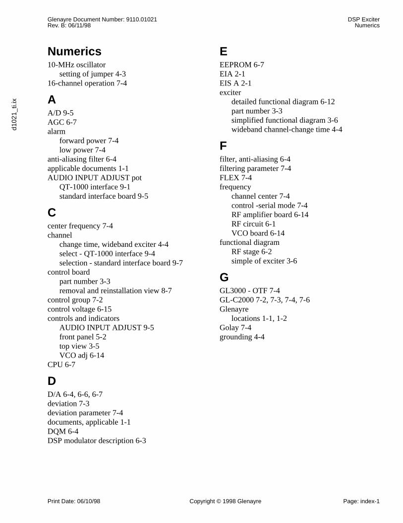
Glenayre Document Number: 9110.01021 DSP ExciterRev. B: 06/11/98 Numerics
d102
1_ti.
ix
Print Date: 06/10/98 Copyright © 1998 Glenayre Page: index-1
Numerics10-MHz oscillator
setting of jumper 4-316-channel operation 7-4
AA/D 9-5AGC 6-7alarm
forward power 7-4low power 7-4
anti-aliasing filter 6-4applicable documents 1-1AUDIO INPUT ADJUST pot
QT-1000 interface 9-1standard interface board 9-5
Ccenter frequency 7-4channel
change time, wideband exciter 4-4select - QT-1000 interface 9-4selection - standard interface board 9-7
control boardpart number 3-3removal and reinstallation view 8-7
control group 7-2control voltage 6-15controls and indicators
AUDIO INPUT ADJUST 9-5front panel 5-2top view 3-5VCO adj 6-14
CPU 6-7
DD/A 6-4, 6-6, 6-7deviation 7-3deviation parameter 7-4documents, applicable 1-1DQM 6-4DSP modulator description 6-3
EEEPROM 6-7EIA 2-1EIS A 2-1exciter
detailed functional diagram 6-12part number 3-3simplified functional diagram 3-6wideband channel-change time 4-4
Ffilter, anti-aliasing 6-4filtering parameter 7-4FLEX 7-4frequency
channel center 7-4control -serial mode 7-4RF amplifier board 6-14RF circuit 6-1VCO board 6-14
functional diagramRF stage 6-2simple of exciter 3-6
GGL3000 - OTF 7-4GL-C2000 7-2, 7-3, 7-4, 7-6Glenayre
locations 1-1, 1-2Golay 7-4grounding 4-4
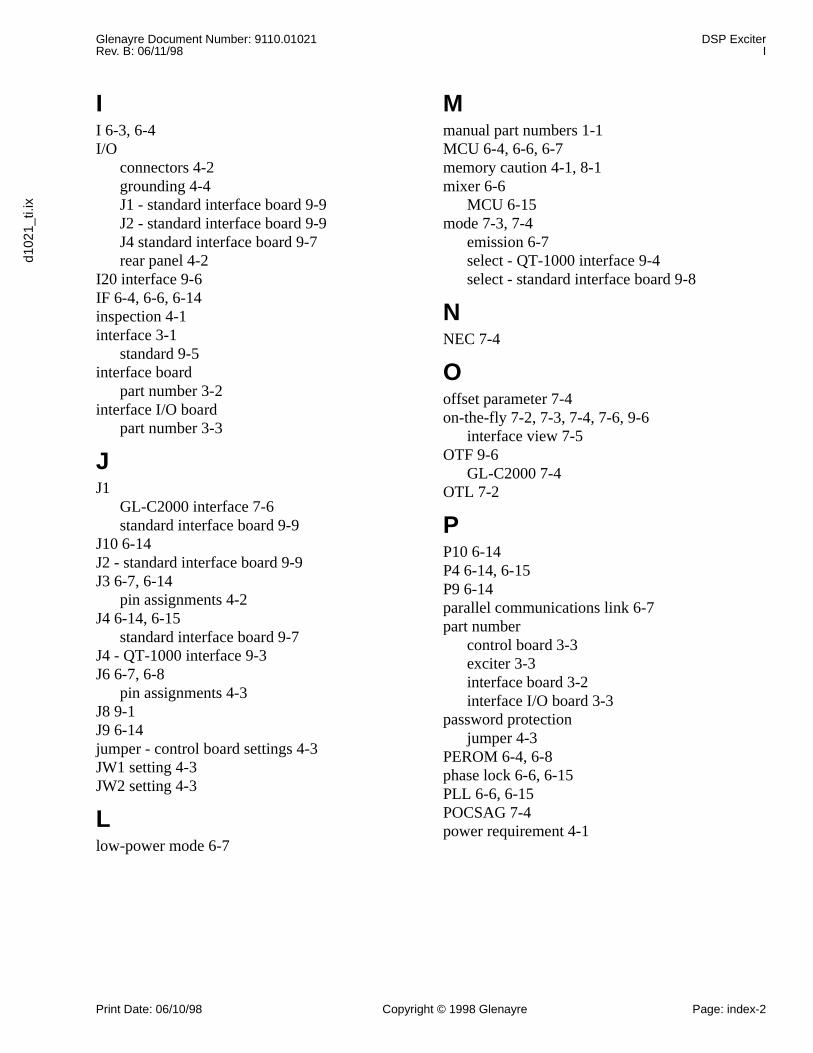
Glenayre Document Number: 9110.01021 DSP ExciterRev. B: 06/11/98 I
d102
1_ti.
ix
Print Date: 06/10/98 Copyright © 1998 Glenayre Page: index-2
II 6-3, 6-4I/O
connectors 4-2grounding 4-4J1 - standard interface board 9-9J2 - standard interface board 9-9J4 standard interface board 9-7rear panel 4-2
I20 interface 9-6IF 6-4, 6-6, 6-14inspection 4-1interface 3-1
standard 9-5interface board
part number 3-2interface I/O board
part number 3-3
JJ1
GL-C2000 interface 7-6standard interface board 9-9
J10 6-14J2 - standard interface board 9-9J3 6-7, 6-14
pin assignments 4-2J4 6-14, 6-15
standard interface board 9-7J4 - QT-1000 interface 9-3J6 6-7, 6-8
pin assignments 4-3J8 9-1J9 6-14jumper - control board settings 4-3JW1 setting 4-3JW2 setting 4-3
Llow-power mode 6-7
Mmanual part numbers 1-1MCU 6-4, 6-6, 6-7memory caution 4-1, 8-1mixer 6-6
MCU 6-15mode 7-3, 7-4
emission 6-7select - QT-1000 interface 9-4select - standard interface board 9-8
NNEC 7-4
Ooffset parameter 7-4on-the-fly 7-2, 7-3, 7-4, 7-6, 9-6
interface view 7-5OTF 9-6
GL-C2000 7-4OTL 7-2
PP10 6-14P4 6-14, 6-15P9 6-14parallel communications link 6-7part number
control board 3-3exciter 3-3interface board 3-2interface I/O board 3-3
password protectionjumper 4-3
PEROM 6-4, 6-8phase lock 6-6, 6-15PLL 6-6, 6-15POCSAG 7-4power requirement 4-1
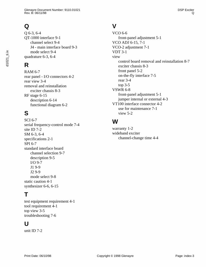
Glenayre Document Number: 9110.01021 DSP ExciterRev. B: 06/11/98 Q
d102
1_ti.
ix
Print Date: 06/10/98 Copyright © 1998 Glenayre Page: index-3
QQ 6-3, 6-4QT-1000 interface 9-1
channel select 9-4J4 - main interface board 9-3mode select 9-4
quadrature 6-3, 6-4
RRAM 6-7rear panel - I/O connectors 4-2rear view 3-4removal and reinstallation
exciter chassis 8-3RF stage 6-15
description 6-14functional diagram 6-2
SSCI 6-7serial frequency-control mode 7-4site ID 7-2SM 6-3, 6-4specifications 2-1SPI 6-7standard interface board
channel selection 9-7description 9-5I/O 9-7J1 9-9J2 9-9mode select 9-8
static caution 4-1synthesizer 6-6, 6-15
Ttest equipment requirement 4-1tool requirement 4-1top view 3-5troubleshooting 7-6
Uunit ID 7-2
VVCO 6-6
front-panel adjustment 5-1VCO ADJ 6-15, 7-1VCO-2 adjustment 7-1VDT 3-1view
control board removal and reinstallation 8-7exciter chassis 8-3front panel 5-2on-the-fly interface 7-5rear 3-4top 3-5
VSWR 6-8front-panel adjustment 5-1jumper internal or external 4-3
VT100 interface connector 4-2use for maintenance 7-1view 5-2
Wwarranty 1-2wideband exciter
channel-change time 4-4
DSP Exciter Glenayre Document Number: 9110.01021W Rev. B: 06/11/98
Page: index-4 Copyright © 1998 Glenayre Print Date: 06/10/98