![· PDF file · 2016-11-23Obtain an expression of the total DSB SC signal. [4+12] (a) Describe generation of FM carrier by Transistor reactance modulator with necessary diagrams. (b)](https://static.fdocuments.net/doc/165x107/5aaefa547f8b9aa8438cbbe4/2016-11-23obtain-an-expression-of-the-total-dsb-sc-signal-412-a-describe.jpg)
DSB & SSB MODULATION - velchuriblog.files.wordpress.com · 1. Balanced Modulator 2. Ring Modulator...
26
ANALOG COMMUNICATIONS VELCHURI 1 [email protected] 8985274654 UNIT-II DSB & SSB MODULATION Syllabus: DSBSC Time and Frequency domain description-Bandwidth of DSB-SC wave, Power calculation in DSB-SC Wave, Generation of DSBSC Waves-Balanced Modulator, Ring modulator, Coherent detection of DSB-SC Modulated Wave-Effect of Phase Error, Effect of Frequency Error and COSTAS Loop. SSBSC Time and Frequency domain description-Power Relations in SSB-Wave, Generation methods of AM SSB Waves -Frequency discrimination, Phase discrimination, Weavers method, Demodulation of SSB Waves-Coherent Detection, Envelop Detector, VSB modulation: Time and Frequency domain description, Generation of VSB Modulated wave, Comparison of AM Techniques, Applications of different AM Systems. Disadvantages of Standard AM wave: ❖ Due to large time constant, some distortion occurs which is known as diagonal clipping i.e., selection of time constant is somewhat difficult. ❖ Power wastage takes place in DSB-FC transmission. ❖ DSB-FC is bandwidth inefficient system. What is DSB-SC and Why? ❖ The equation of single tone AM wave is expressed as ()= A c cosω c t+ µ 2 [cos( + )] + µ 2 [cos( − )] ❖ In power calculation of AM signal, it has been observed that for single-tone sinusoidal modulation, for 100% modulation about 67% of the total power is required for transmitting the carrier which does not contain any information. ❖ Hence, if the carrier is supressed, only the sidebands remain and in this way a saving of two-third power may be achieved at 100% modulation. ❖ The signal resulting from suppressing carrier from the modulated signal and remains only TWO side bands is called DSB-SC Wave. DSB-SC Time & Frequency domain analysis ❖ A DSB-SC signal can be obtained by simply multiplying modulating signal with carrier signal. So we need to use a device called product modulator for the generation of DSB-SC wave. ❖ The single-tone DSB-SC in time-domain is given by (t) = ()A c cosω c t=A m cosω t. A c cosω c t=A m A c cosω t. cosω c t = A m 2 [cos( + )] + A m 2 [cos( − )] ❖ The single-tone DSB-SC in Frequency-domain is given by (ω)= A m 2 [( − ( + )) + ( + ( + ))] + A m 2 [( − ( − )) + ( + ( − ))]
Transcript of DSB & SSB MODULATION - velchuriblog.files.wordpress.com · 1. Balanced Modulator 2. Ring Modulator...
ANALOG COMMUNICATIONS VELCHURI
1 [email protected] 8985274654
UNIT-II
DSB & SSB MODULATION
Syllabus: DSBSC Time and Frequency domain description-Bandwidth of DSB-SC wave, Power calculation in DSB-SC Wave, Generation of DSBSC Waves-Balanced Modulator, Ring modulator, Coherent detection of DSB-SC Modulated Wave-Effect of Phase Error, Effect of Frequency Error and COSTAS Loop. SSBSC Time and Frequency domain description-Power Relations in SSB-Wave, Generation methods of AM SSB Waves -Frequency discrimination, Phase discrimination, Weavers method, Demodulation of SSB Waves-Coherent Detection, Envelop Detector, VSB modulation: Time and Frequency domain description, Generation of VSB Modulated wave, Comparison of AM Techniques, Applications of different AM Systems.
Disadvantages of Standard AM wave:
❖ Due to large time constant, some distortion occurs which is known as diagonal
clipping i.e., selection of time constant is somewhat difficult.
❖ Power wastage takes place in DSB-FC transmission.
❖ DSB-FC is bandwidth inefficient system.
What is DSB-SC and Why?
❖ The equation of single tone AM wave is expressed as
𝑆𝐴𝑀(𝑡)= Accosωct + µ𝐴𝑐
2[cos(𝜔𝑐 + 𝜔𝑚)] +
µ𝐴𝑐
2[cos(𝜔𝑐 − 𝜔𝑚)]
❖ In power calculation of AM signal, it has been observed that for single-tone sinusoidal
modulation, for 100% modulation about 67% of the total power is required for
transmitting the carrier which does not contain any information.
❖ Hence, if the carrier is supressed, only the sidebands remain and in this way a saving
of two-third power may be achieved at 100% modulation.
❖ The signal resulting from suppressing carrier from the modulated signal and remains
only TWO side bands is called DSB-SC Wave.
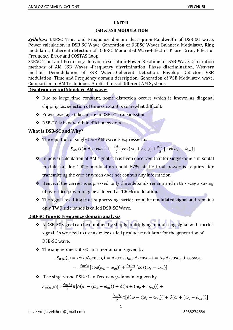
DSB-SC Time & Frequency domain analysis
❖ A DSB-SC signal can be obtained by simply multiplying modulating signal with carrier
signal. So we need to use a device called product modulator for the generation of
DSB-SC wave.
❖ The single-tone DSB-SC in time-domain is given by
𝑆𝐷𝑆𝐵(t) = 𝑚(𝑡)Accosωct = Amcosω𝑚t. Accosωct = AmAccosω𝑚t. cosωct
= Am𝐴𝑐
2[cos(𝜔𝑐 + 𝜔𝑚)] +
Am𝐴𝑐
2[cos(𝜔𝑐 − 𝜔𝑚)]
❖ The single-tone DSB-SC in Frequency-domain is given by
𝑆𝐷𝑆𝐵(ω)= Am𝐴𝑐
2𝜋[𝛿(𝜔 − (𝜔𝑐 + 𝜔𝑚)) + 𝛿(𝜔 + (𝜔𝑐 + 𝜔𝑚))] +
Am𝐴𝑐
2𝜋[𝛿(𝜔 − (𝜔𝑐 − 𝜔𝑚)) + 𝛿(𝜔 + (𝜔𝑐 − 𝜔𝑚))]
ANALOG COMMUNICATIONS VELCHURI
2 [email protected] 8985274654
Figure 2.1 Generation of DSB-SC Wave
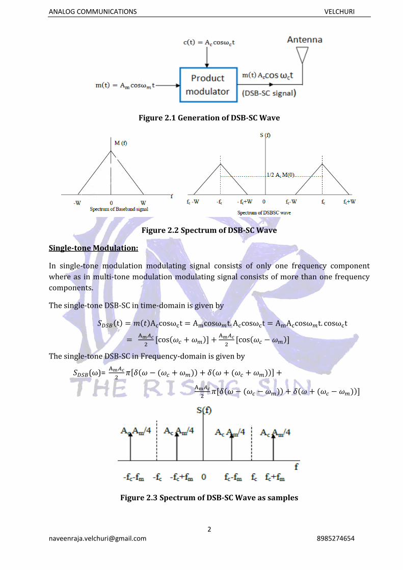
Figure 2.2 Spectrum of DSB-SC Wave
Single-tone Modulation:
In single-tone modulation modulating signal consists of only one frequency component
where as in multi-tone modulation modulating signal consists of more than one frequency
components.
The single-tone DSB-SC in time-domain is given by
𝑆𝐷𝑆𝐵(t) = 𝑚(𝑡)Accosωct = Amcosω𝑚t. Accosωct = AmAccosω𝑚t. cosωct
= Am𝐴𝑐
2[cos(𝜔𝑐 + 𝜔𝑚)] +
Am𝐴𝑐
2[cos(𝜔𝑐 − 𝜔𝑚)]
The single-tone DSB-SC in Frequency-domain is given by
𝑆𝐷𝑆𝐵(ω)= Am𝐴𝑐
2𝜋[𝛿(𝜔 − (𝜔𝑐 + 𝜔𝑚)) + 𝛿(𝜔 + (𝜔𝑐 + 𝜔𝑚))] +
Am𝐴𝑐
2𝜋[𝛿(𝜔 − (𝜔𝑐 − 𝜔𝑚)) + 𝛿(𝜔 + (𝜔𝑐 − 𝜔𝑚))]
Figure 2.3 Spectrum of DSB-SC Wave as samples
ANALOG COMMUNICATIONS VELCHURI
3 [email protected] 8985274654
Power Calculation in DSB-SC Wave:
𝑃𝐷𝑆𝐵 = 𝑃𝐿𝑆𝐵 + 𝑃𝑈𝑆𝐵 =𝐴𝑚
2 . 𝐴𝑐2
8+
𝐴𝑚2 . 𝐴𝑐
2
8=
𝐴𝑚2 . 𝐴𝑐
2
4
Percentage of Power saving in DSB-SC Wave:
Note:
✓ The time domain displays of DSB-FC with 100% and DSB-SC signal looks exactly
same. The only difference is carrier undergoes 1800in DSB-SC .
✓ The bandwidth of DSB-SC is same that of DSB-FC wave, that is 2fm.
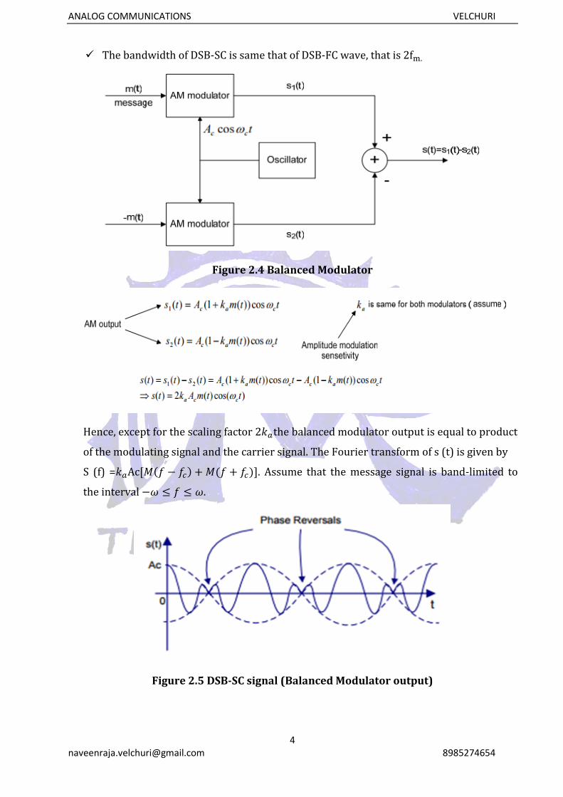
Generation of DSB-SC Wave:
To generate DSB-SC wave, two methods are available. They are
1. Balanced Modulator
2. Ring Modulator
❖ Balanced Modulator:
✓ DSB-SC is obtained by using two AM modulators arranged in a balanced
configuration to cancel out the carrier.
✓ The input applied to the top AM modulator is m(t), whereas that applied to the lower
AM modulator is – m(t).
✓ These two AM modulators should connect in balanced configuration.
✓ These two modulators have the same amplitude sensitivity.
✓ The time domain displays of DSB-FC with 100% and DSB-SC signal looks exactly
same. The only difference is carrier undergoes 1800in DSB-SC.
ANALOG COMMUNICATIONS VELCHURI
4 [email protected] 8985274654
✓ The bandwidth of DSB-SC is same that of DSB-FC wave, that is 2fm.
Figure 2.4 Balanced Modulator
Hence, except for the scaling factor 2𝑘𝑎the balanced modulator output is equal to product
of the modulating signal and the carrier signal. The Fourier transform of s (t) is given by
S (f) =𝑘𝑎Ac[𝑀(𝑓 − 𝑓𝑐) + 𝑀(𝑓 + 𝑓𝑐)]. Assume that the message signal is band-limited to
the interval −𝜔 ≤ 𝑓 ≤ 𝜔.
Figure 2.5 DSB-SC signal (Balanced Modulator output)
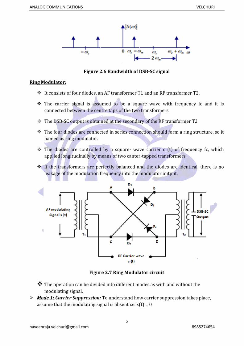
ANALOG COMMUNICATIONS VELCHURI
5 [email protected] 8985274654
Figure 2.6 Bandwidth of DSB-SC signal
Ring Modulator:
❖ It consists of four diodes, an AF transformer T1 and an RF transformer T2.
❖ The carrier signal is assumed to be a square wave with frequency fc and it is
connected between the centre taps of the two transformers.
❖ The DSB-SC output is obtained at the secondary of the RF transformer T2
❖ The four diodes are connected in series connection should form a ring structure, so it
named as ring modulator.
❖ The diodes are controlled by a square- wave carrier c (t) of frequency fc, which
applied longitudinally by means of two canter-tapped transformers.
❖ If the transformers are perfectly balanced and the diodes are identical, there is no
leakage of the modulation frequency into the modulator output.
Figure 2.7 Ring Modulator circuit
❖ The operation can be divided into different modes as with and without the
modulating signal.
➢ Mode 1: Carrier Suppression: To understand how carrier suppression takes place,
assume that the modulating signal is absent i.e. x(t) = 0
ANALOG COMMUNICATIONS VELCHURI
6 [email protected] 8985274654
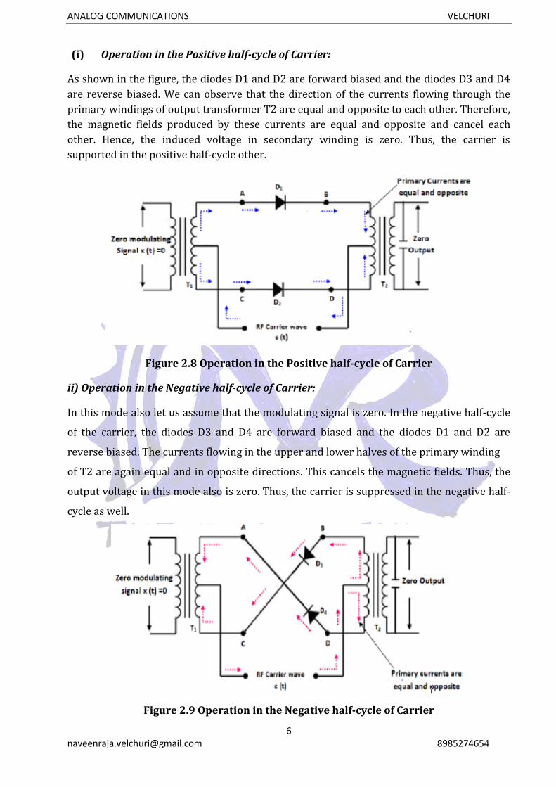
(i) Operation in the Positive half-cycle of Carrier:
As shown in the figure, the diodes D1 and D2 are forward biased and the diodes D3 and D4
are reverse biased. We can observe that the direction of the currents flowing through the
primary windings of output transformer T2 are equal and opposite to each other. Therefore,
the magnetic fields produced by these currents are equal and opposite and cancel each
other. Hence, the induced voltage in secondary winding is zero. Thus, the carrier is
supported in the positive half-cycle other.
Figure 2.8 Operation in the Positive half-cycle of Carrier
ii) Operation in the Negative half-cycle of Carrier:
In this mode also let us assume that the modulating signal is zero. In the negative half-cycle
of the carrier, the diodes D3 and D4 are forward biased and the diodes D1 and D2 are
reverse biased. The currents flowing in the upper and lower halves of the primary winding
of T2 are again equal and in opposite directions. This cancels the magnetic fields. Thus, the
output voltage in this mode also is zero. Thus, the carrier is suppressed in the negative half-
cycle as well.
Figure 2.9 Operation in the Negative half-cycle of Carrier
ANALOG COMMUNICATIONS VELCHURI
7 [email protected] 8985274654
It is important to note that the perfect cancellation of the carrier will take place if and only if
he characteristics of the diodes are perfectly matched and the center-tap is placed exactly at
the center of the primary transformer T2.
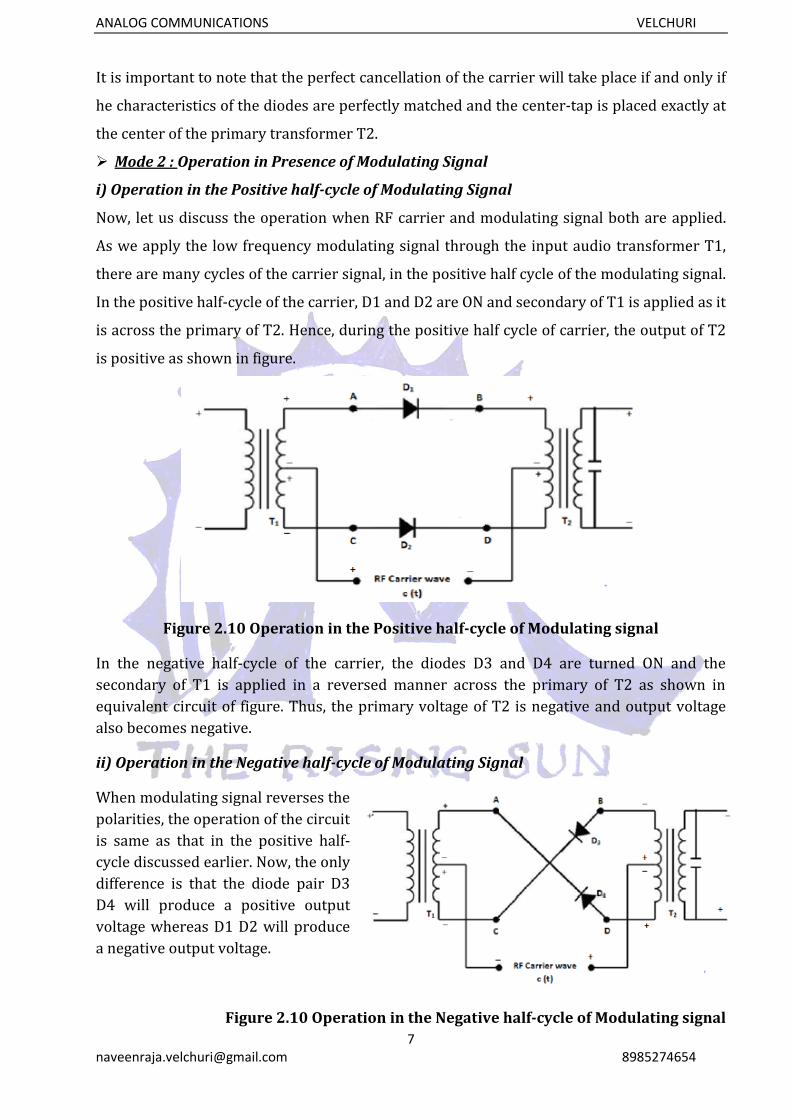
➢ Mode 2 : Operation in Presence of Modulating Signal
i) Operation in the Positive half-cycle of Modulating Signal
Now, let us discuss the operation when RF carrier and modulating signal both are applied.
As we apply the low frequency modulating signal through the input audio transformer T1,
there are many cycles of the carrier signal, in the positive half cycle of the modulating signal.
In the positive half-cycle of the carrier, D1 and D2 are ON and secondary of T1 is applied as it
is across the primary of T2. Hence, during the positive half cycle of carrier, the output of T2
is positive as shown in figure.
Figure 2.10 Operation in the Positive half-cycle of Modulating signal
In the negative half-cycle of the carrier, the diodes D3 and D4 are turned ON and the
secondary of T1 is applied in a reversed manner across the primary of T2 as shown in
equivalent circuit of figure. Thus, the primary voltage of T2 is negative and output voltage
also becomes negative.
ii) Operation in the Negative half-cycle of Modulating Signal
When modulating signal reverses the
polarities, the operation of the circuit
is same as that in the positive half-
cycle discussed earlier. Now, the only
difference is that the diode pair D3
D4 will produce a positive output
voltage whereas D1 D2 will produce
a negative output voltage.
Figure 2.10 Operation in the Negative half-cycle of Modulating signal
ANALOG COMMUNICATIONS VELCHURI
8 [email protected] 8985274654
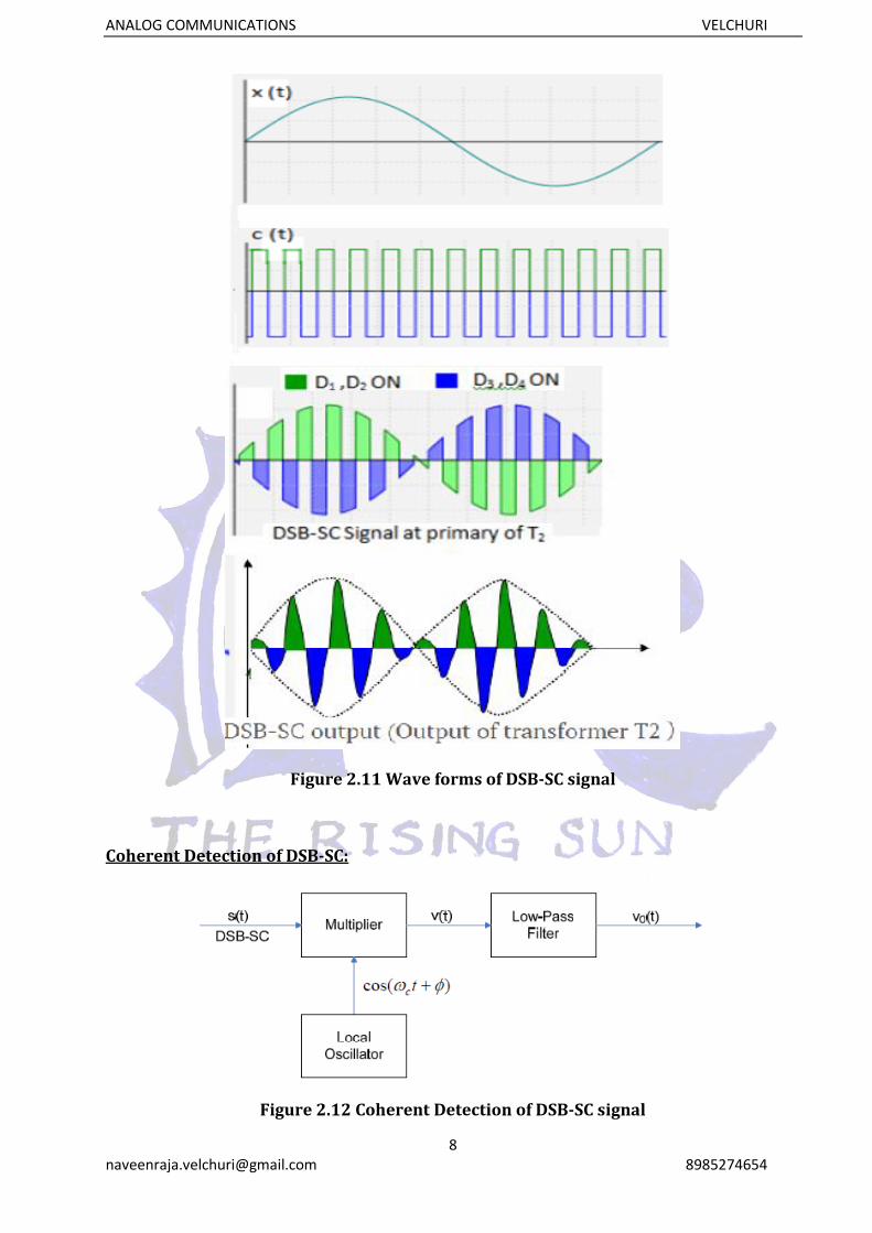
Figure 2.11 Wave forms of DSB-SC signal
Coherent Detection of DSB-SC:
Figure 2.12 Coherent Detection of DSB-SC signal
ANALOG COMMUNICATIONS VELCHURI
9 [email protected] 8985274654
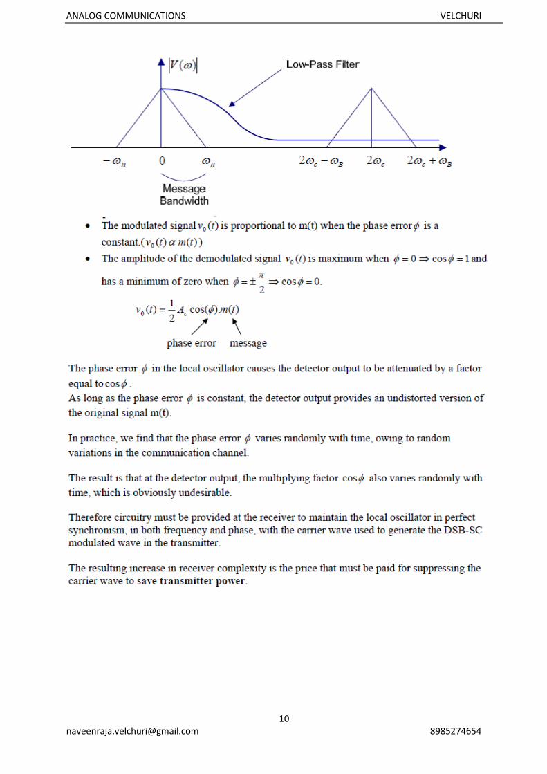
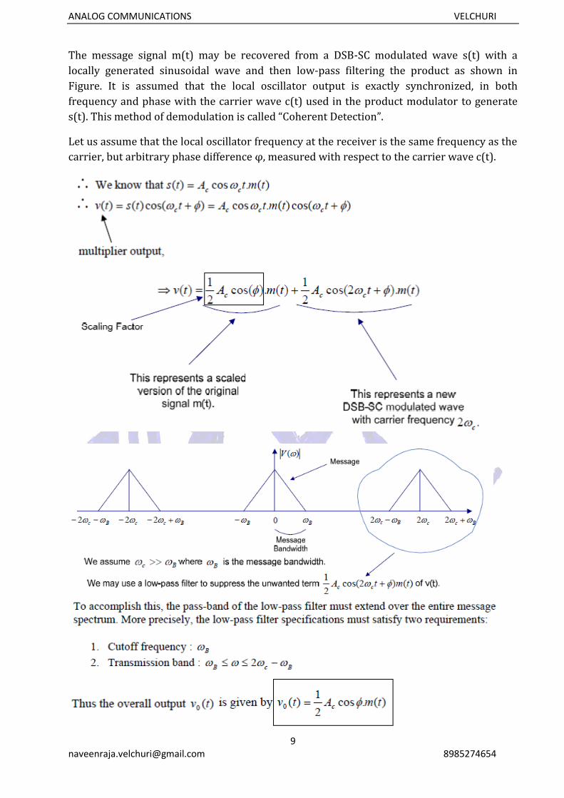
The message signal m(t) may be recovered from a DSB-SC modulated wave s(t) with a
locally generated sinusoidal wave and then low-pass filtering the product as shown in
Figure. It is assumed that the local oscillator output is exactly synchronized, in both
frequency and phase with the carrier wave c(t) used in the product modulator to generate
s(t). This method of demodulation is called “Coherent Detection”.
Let us assume that the local oscillator frequency at the receiver is the same frequency as the
carrier, but arbitrary phase difference φ, measured with respect to the carrier wave c(t).
ANALOG COMMUNICATIONS VELCHURI
12 [email protected] 8985274654
Synchroniztion techniques in DSB-SC:
Pilot Carrier:
✓ A small amount of carrier known as pilot carrier is transmitted along with the
modulated signal from transmitter. It is separated at receiver with appropriate filter.
✓ This system, where a weak carrier signal transmitted along with DSB-SC signal is
known as partially suppressed carrier system.
✓ DSB-SC signal with partially suppressed carrier system is equal to over modulated AM
signal.
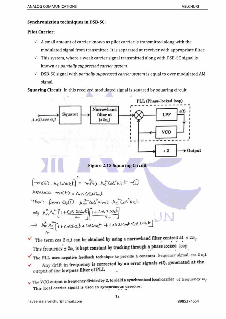
Squaring Circuit: In this received modulated signal is squared by squaring circuit.
Figure 2.13 Squaring Circuit
ANALOG COMMUNICATIONS VELCHURI
13 [email protected] 8985274654
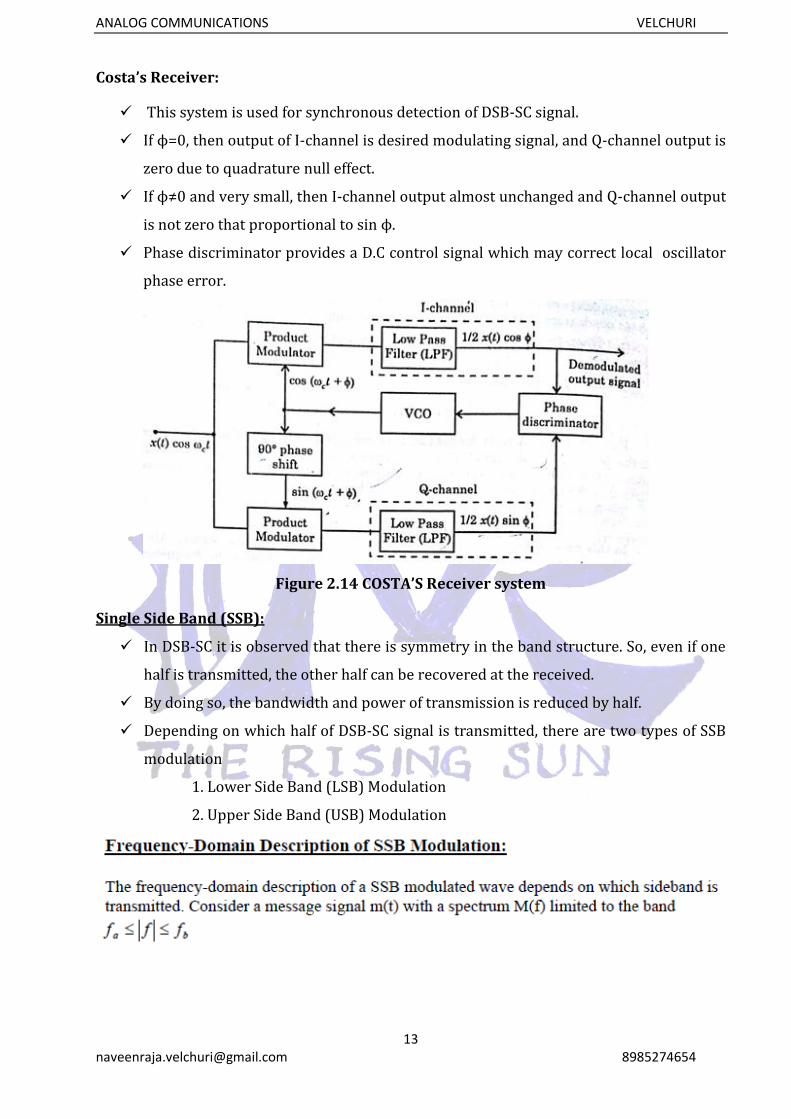
Costa’s Receiver:
✓ This system is used for synchronous detection of DSB-SC signal.
✓ If ϕ=0, then output of I-channel is desired modulating signal, and Q-channel output is
zero due to quadrature null effect.
✓ If ϕ≠0 and very small, then I-channel output almost unchanged and Q-channel output
is not zero that proportional to sin ϕ.
✓ Phase discriminator provides a D.C control signal which may correct local oscillator
phase error.
Figure 2.14 COSTA’S Receiver system
Single Side Band (SSB):
✓ In DSB-SC it is observed that there is symmetry in the band structure. So, even if one
half is transmitted, the other half can be recovered at the received.
✓ By doing so, the bandwidth and power of transmission is reduced by half.
✓ Depending on which half of DSB-SC signal is transmitted, there are two types of SSB
modulation
1. Lower Side Band (LSB) Modulation
2. Upper Side Band (USB) Modulation
ANALOG COMMUNICATIONS VELCHURI
14 [email protected] 8985274654
Generation of Single Side Band (SSB):
There are two generation techniques are available for SSB modulated wave. They are
1. Filter method (Frequency Discrimination)
2. Phase-shift method.
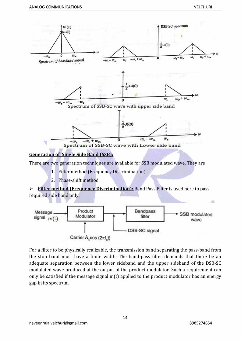
➢ Filter method (Frequency Discrimination): Band Pass Filter is used here to pass
required side band only.
For a filter to be physically realizable, the transmission band separating the pass-band from
the stop band must have a finite width. The band-pass filter demands that there be an
adequate separation between the lower sideband and the upper sideband of the DSB-SC
modulated wave produced at the output of the product modulator. Such a requirement can
only be satisfied if the message signal m(t) applied to the product modulator has an energy
gap in its spectrum
ANALOG COMMUNICATIONS VELCHURI
15 [email protected] 8985274654
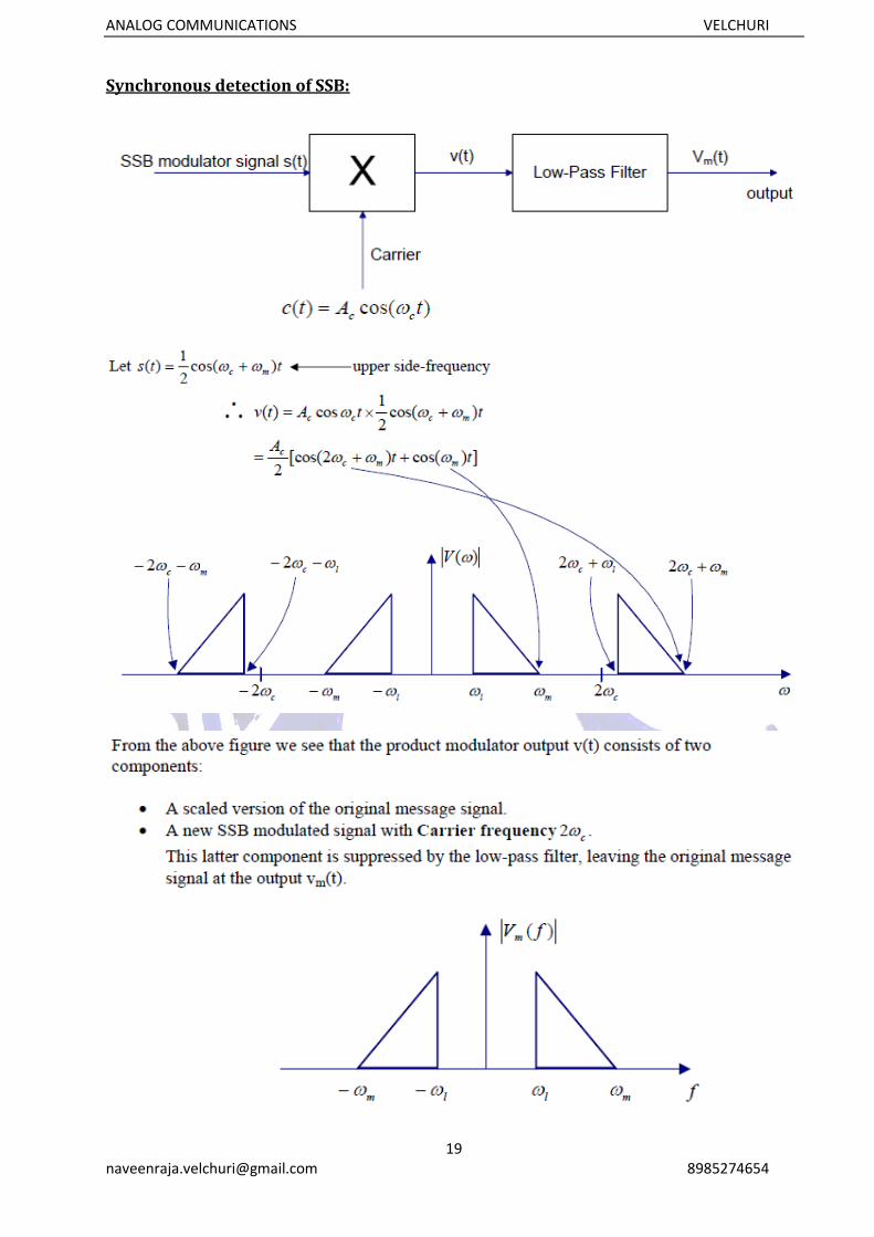
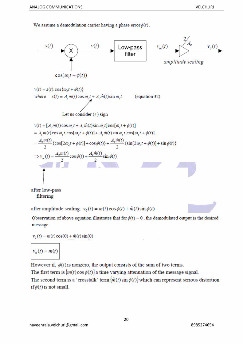
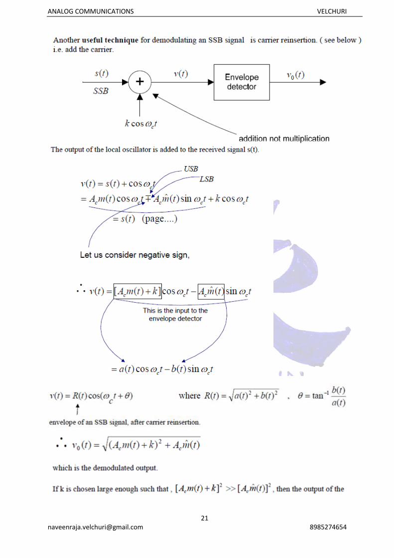
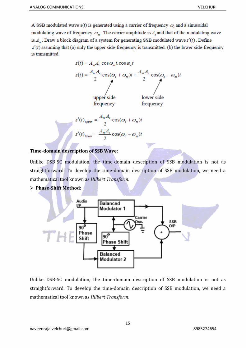
Time-domain description of SSB Wave:
Unlike DSB-SC modulation, the time-domain description of SSB modulation is not as
straightforward. To develop the time-domain description of SSB modulation, we need a
mathematical tool known as Hilbert Transform.
➢ Phase-Shift Method:
Unlike DSB-SC modulation, the time-domain description of SSB modulation is not as
straightforward. To develop the time-domain description of SSB modulation, we need a
mathematical tool known as Hilbert Transform.
ANALOG COMMUNICATIONS VELCHURI
18 [email protected] 8985274654
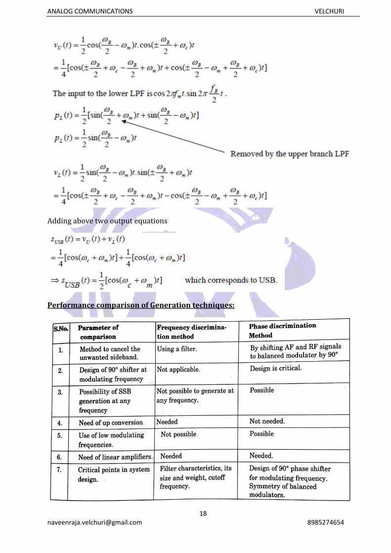
Adding above two output equations
Performance comparison of Generation techniques:
ANALOG COMMUNICATIONS VELCHURI
22 [email protected] 8985274654
❖ Power saving in SSB System:
❖ Advantages of SSB:
❖ Disadvantages of SSB:
❖ Applications of SSB:
ANALOG COMMUNICATIONS VELCHURI
23 [email protected] 8985274654
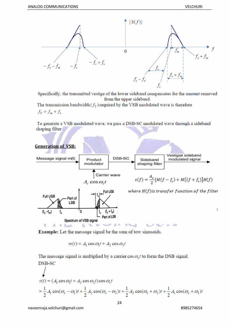
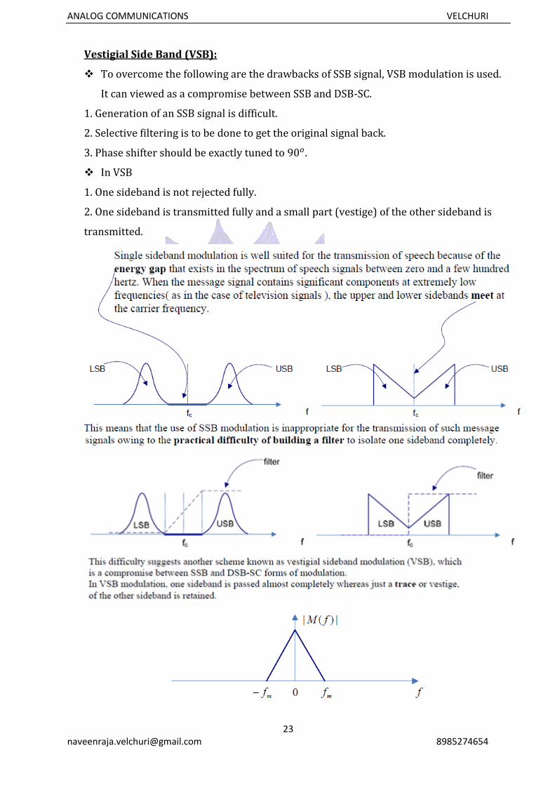
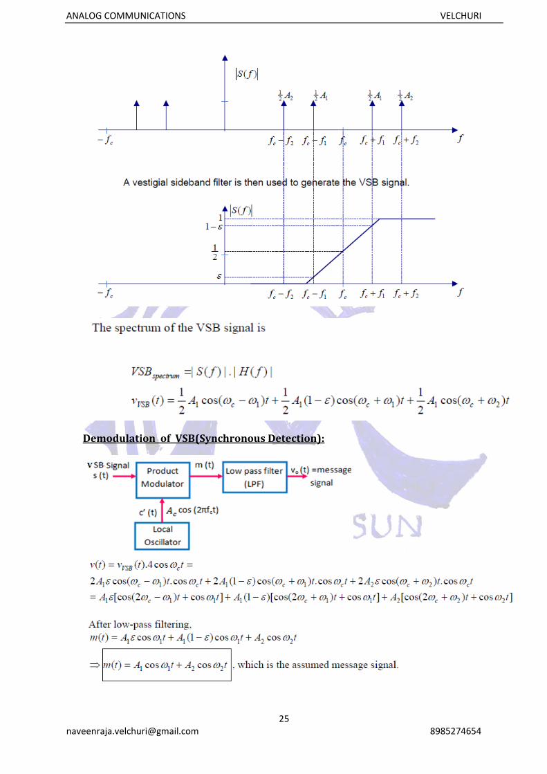
Vestigial Side Band (VSB):
❖ To overcome the following are the drawbacks of SSB signal, VSB modulation is used.
It can viewed as a compromise between SSB and DSB-SC.
1. Generation of an SSB signal is difficult.
2. Selective filtering is to be done to get the original signal back.
3. Phase shifter should be exactly tuned to 90𝑜 .
❖ In VSB
1. One sideband is not rejected fully.
2. One sideband is transmitted fully and a small part (vestige) of the other sideband is
transmitted.
ANALOG COMMUNICATIONS VELCHURI
25 [email protected] 8985274654
Demodulation of VSB(Synchronous Detection):
ANALOG COMMUNICATIONS VELCHURI
26 [email protected] 8985274654
Transmission bandwidth of VSB is
VSB Modulation − Advantages:
✓ Highly efficient.
✓ Reduction in bandwidth.
✓ Filter design is easy as high accuracy is not needed.
✓ The transmission of low frequency components is possible.
✓ Possesses good phase characteristics.
VSB Modulation − Disadvantages:
✓ Bandwidth when compared to SSB is greater.
✓ Demodulation is complex.
VSB Modulation − Applications:
✓ Used for the transmission of television signals.
✓ This is the most convenient and efficient technique when bandwidth usage is
considered.
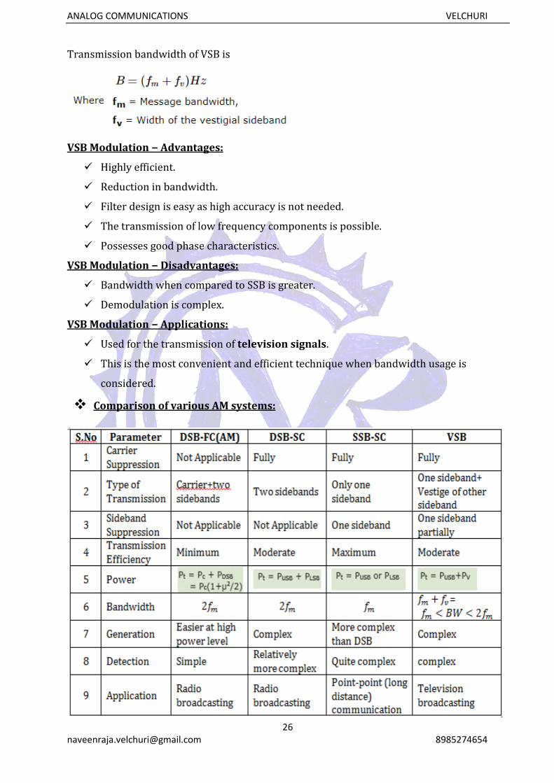
❖ Comparison of various AM systems: