DS90UR90xQ-Q1 5- to 65-MHz, 24-bit Color FPD-Link II Serializer ...

MIPI CSI-2
Processor SoC
DS90UB964-Q1 FPD-Link III HUB
D3P/N
CLKP/N
FPD-Link III Serializer
I2C
GPIO
FPD-Link IIICoax or STP
FPD-Link III Serializer
FPD-Link III Serializer
FPD-Link III Serializer
D2P/N
D1P/N
D0P/N
Product
Folder
Sample &Buy
Technical
Documents
Tools &
Software
Support &Community
An IMPORTANT NOTICE at the end of this data sheet addresses availability, warranty, changes, use in safety-critical applications,intellectual property matters and other important disclaimers. PRODUCTION DATA.
DS90UB964-Q1SNLS500 –JULY 2016
DS90UB964-Q1 Quad FPD-Link III Deserializer Hub
1
1 Features1• Qualified for Automotive Applications• AEC-Q100 Qualified With the Following Results:
– Device Temperature Grade 2: –40 to +105Ambient Operating Temperature Range
– Device HBM ESD Classification Level ±4 kV– Device CDM ESD Classification Level C6
• Aggregates Data From up to 4 Cameras OverFPD-Link III Interface
• Supports 1-Megapixel Sensors With HD720p/800p/960p Resolution at 30-Hz or 60-HzFrame Rate
• Multi-Camera Synchronization• MIPI DPHY Version 1.2 / CSI-2 Version 1.3
Compliant– 2× CSI-2 Output Ports– Supports 1, 2, 3, 4 Data Lanes per CSI-2 port– CSI-2 Data Rate Scalable for 400 Mbps / 800
Mbps / 1.5 Gbps / 1.6 Gbps each Data Lane– Programmable Data Types– Four Virtual Channels– ECC and CRC Generation
• Supports Single-Ended Coaxial or ShieldedTwisted-Pair (STP) Cable
• Adaptive Receive Equalization• I2C With Fast-Mode Plus up to 1 Mbps• Flexible GPIOs for Camera Sync and Functional
Safety• Compatible With DS90UB913AQ/913Q/933Q
Serializers• CRC protection on the internal Data Path• ISO 10605 and IEC 61000-4-2 ESD Compliant
2 Applications• Automotive ADAS
– Surround View Systems– Camera Monitoring Systems– Sensor Fusion
• Security and Surveillance
3 DescriptionThe DS90UB964-Q1 is a versatile camera hubcapable of connecting serialized camera datareceived from 4 independent video datastreams viaan FPD-Link III interface. When coupled withDS90UB913AQ/913Q/933Q serializers, theDS90UB964-Q1 receives data from 1-Megapixelimage sensors supporting 720p/800p/960p resolutionat 30-Hz or 60-Hz frame rates. Data is received andaggregated into a MIPI CSI-2 compliant output forinterconnect to a downstream processor. A secondMIPI CSI-2 output port is available to provideadditional bandwidth, or offers a second replicatedoutput.
The DS90UB964-Q1 includes 4 FPD-Link IIIdeserializers, each enabling a connection via cost-effective 50-Ω single-ended coaxial or 100-Ωdifferential STP cables. The receive equalizerautomatically adapts to compensate for cable losscharacteristics, including degradation over time.
Each of the FPD-Link III interfaces also includes aseparate low latency bi-directional control channelthat conveys control information from an I2C port andis independent of video blanking period. Generalpurpose I/O signals such as those required forcamera synchronization and functional safetyfeatures also make use of this bi-directional controlchannel.
Device Information(1)
PART NUMBER PACKAGE BODY SIZE (NOM)DS90UB964-Q1 VQFN (64) 9.00 mm × 9.00 mm
(1) For all available packages, see the orderable addendum atthe end of the data sheet.
Typical Application Schematic

2
DS90UB964-Q1SNLS500 –JULY 2016 www.ti.com
Product Folder Links: DS90UB964-Q1
Submit Documentation Feedback Copyright © 2016, Texas Instruments Incorporated
Table of Contents1 Features .................................................................. 12 Applications ........................................................... 13 Description ............................................................. 14 Revision History..................................................... 25 Pin Configuration and Functions ......................... 36 Specifications......................................................... 6
6.1 Absolute Maximum Ratings ...................................... 66.2 ESD Ratings – JEDEC.............................................. 66.3 ESD Ratings – IEC and ISO ..................................... 66.4 Recommended Operating Conditions....................... 66.5 Thermal Information .................................................. 76.6 DC Electrical Characteristics ................................... 76.7 AC Electrical Characteristics................................... 106.8 Recommended Timing for the Serial Control Bus .. 116.9 AC Electrical Characteristics................................... 12
7 Typical Characteristics........................................ 198 Detailed Description ............................................ 20
8.1 Overview ................................................................. 208.2 Functional Block Diagram ....................................... 208.3 Feature Description................................................. 208.4 Device Functional Modes........................................ 218.5 Programming .......................................................... 39
8.6 Register Description................................................ 508.7 Register Maps ......................................................... 51
9 Application and Implementation ........................ 989.1 Application Information............................................ 989.2 Typical Application ................................................. 999.3 System Examples ................................................ 101
10 Power Supply Recommendations ................... 10310.1 VDD Power Supply ............................................. 10310.2 Power-Up Sequencing ........................................ 10310.3 PDB Pin............................................................... 10310.4 Ground ................................................................ 104
11 Layout................................................................. 10511.1 Layout Guidelines ............................................... 10511.2 Layout Example .................................................. 106
12 Device and Documentation Support ............... 10812.1 Documentation Support ..................................... 10812.2 Receiving Notification of Documentation
Updates.................................................................. 10812.3 Community Resources........................................ 10812.4 Trademarks ......................................................... 10812.5 Electrostatic Discharge Caution.......................... 10812.6 Glossary .............................................................. 108
4 Revision History
DATE REVISION NOTESJuly 2016 * Initial release.

RIN0-
PD
B
TE
ST
EN
VD
D18
_P2
VDD18_FPD1
CMLOUTN
CMLOUTP
VDD18_FPD2
RIN2+
RIN2-
GP
IO[3
]
CSI0_D2P
CSI0_CLKP
VD
D18
_P0
CSI0_D3N
CSI0_D3P
GP
IO[0
]
I2C
_SC
L2
CSI0_D1P
CSI0_D2N
VD
DIO
CSI0_D1N
VDD_CSI0
CSI0_CLKN
RIN3+
VDD_FPD2
VD
D18
_P3
RIN3-
VDD18_FPD3
1 2 3 4 5 6 7 8 9 10 11 12 13 14 15 16
32
31
30
29
28
27
26
25
24
23
22
21
20
19
18
17
48 47 46 45 44 43 42 41 40 39 38 37 36 35 34 33
49
50
51
52
53
54
55
56
57
58
59
60
61
62
63
64
VDD_FPD1
CS
I1_D
0P
CS
I1_D
1N
RIN1-
GPIO[7]
GPIO[5]
GPIO[6]
CS
I1_D
3P
VDD18_FPD0
RIN0+
CS
I1_D
2P
CS
I1_D
1P
CS
I1_D
2N
INT
B
I2C
_SD
A2
CSI0_D0P
CSI0_D0N
VD
DL
2
VD
D18
_P1
MO
DE
IDX
GP
IO[2
]
VD
DL
1
I2C
_SC
L
I2C
_SD
A
VD
D_C
SI1
CS
I1_D
0N
CS
I1_C
LKN
CS
I1_C
LKP
GP
IO[1
]
VDD18A
RIN1+
CS
I1_D
3N
RE
FC
LK
DS90UB964-Q164L QFN
Top down view
DAP
GPIO[4]
3
DS90UB964-Q1www.ti.com SNLS500 –JULY 2016
Product Folder Links: DS90UB964-Q1
Submit Documentation FeedbackCopyright © 2016, Texas Instruments Incorporated
5 Pin Configuration and Functions
RGC Package64-Pin VQFN(Top View)
Table 1. Pin FunctionsPIN I/O
TYPE DESCRIPTIONNAME NO.
MIPI DPHY/CSI-2CSI0_CLKN/P 22, 23 O, DPHY CSI0 Differential clock
If unused, leave this pin unconnected.CSI0_D0N/P 24, 25 O, DPHY CSI0 Differential data pair 0
If unused, leave this pin unconnected.CSI0_D1N/P 26, 27 O, DPHY CSI0 Differential data pair 1
If unused, leave this pin unconnected.CSI0_D2N/P 28, 29 O, DPHY CSI0 Differential data pair 2
If unused, leave this pin unconnected.CSI0_D3N/P 30, 31 O, DPHY CSI0 Differential data pair 3
If unused, leave this pin unconnected.CSI1_CLKN/P 34, 35 O, DPHY CSI1 Differential clock
If unused, leave this pin unconnected.CSI1_D0N/P 36, 37 O, DPHY CSI1 Differential data pair 0
If unused, leave this pin unconnected.CSI1_D1N/P 38, 39 O, DPHY CSI1 Differential data pair 1
If unused, leave this pin unconnected.CSI1_D2N/P 40, 41 O, DPHY CSI1 Differential data pair 2
If unused, leave this pin unconnected.

4
DS90UB964-Q1SNLS500 –JULY 2016 www.ti.com
Product Folder Links: DS90UB964-Q1
Submit Documentation Feedback Copyright © 2016, Texas Instruments Incorporated
Table 1. Pin Functions (continued)PIN I/O
TYPE DESCRIPTIONNAME NO.
(1) Optimum Pull-up Resistor (RPU) value depends on the I2C mode of operation, refer to SLVA689
CSI1_D3N/P 42, 43 O, DPHY CSI1 Differential data pair 3If unused, leave this pin unconnected.
FPD-LINK III INTERFACERIN0-/+ 51, 50 I/O, CML FPD-Link III Input/Output. The pin must be AC-coupled with a capacitor.
If port is unused, set RX_PORT_CTL register bit N to 0 to disable.RIN1-/+ 54, 53 I/O, CML FPD-Link III Input/Output. The pin must be AC-coupled with a capacitor.
If port is unused, set RX_PORT_CTL register bit N to 0 to disable.RIN2-/+ 60, 59 I/O, CML FPD-Link III Input/Output. The pin must be AC-coupled with a capacitor.
If port is unused, set RX_PORT_CTL register bit N to 0 to disable.RIN3-/+ 63, 62 I/O, CML FPD-Link III Input/Output. The pin must be AC-coupled with a capacitor.
If port is unused, set RX_PORT_CTL register bit N to 0 to disable.GPIO PINS (GENERAL PURPOSE INPUT OUTPUT)GPIO[0] 9 I/O, LVCMOS,
PDGeneral Purpose Input/Output 0See GPIO Support.
GPIO[1] 10 I/O, LVCMOS,PD
General Purpose Input/Output 1See GPIO Support.
GPIO[2] 14 I/O, LVCMOS,PD
General Purpose Input/Output 2See GPIO Support.
GPIO[3] 15 I/O, LVCMOS,PD
General Purpose Input/Output 3See GPIO Support.
GPIO[4] 17 I/O, LVCMOS,PD
General Purpose Input/Output 4See GPIO Support.
GPIO[5] 18 I/O, LVCMOS,PD
General Purpose Input/Output 5See GPIO Support.
GPIO[6] 19 I/O, LVCMOS,PD
General Purpose Input/Output 6See GPIO Support.
GPIO[7] 20 I/O, LVCMOS,PD
General Purpose Input/Output 7See GPIO Support.
I2C PINSI2C_SCL 12 I/O, LVCMOS,
Open DrainI2C Clock Input / Output InterfaceRecommended Pull-up (1) to 4.7 kΩ to VDDIO.
I2C_SDA 11 I/O, LVCMOS,Open Drain
I2C Data Input / Output InterfaceRecommended Pull-up (1) to 4.7 kΩ to VDDIO.
I2C_SCL2 8 I/O, LVCMOS,Open Drain
I2C Clock Input / Output InterfaceRecommended Pull-up (1) to 4.7 kΩ to VDDIO.
I2C_SDA2 7 I/O, LVCMOS,Open Drain
I2C Data Input / Output InterfaceRecommended Pull-up (1) to 4.7 kΩ to VDDIO.
IDx 46 S I2C Serial Control Bus Device ID AddressConnect to external pull-up to VDD18 and pull-down to GND to create a voltagedivider. See Table 10.
CONTROL PINSMODE 45 S Mode selection
Connect to external pull-up to VDD18 and pull-down to GND to create a voltagedivider. See Table 2.
PDB 3 I, 1.8VLVCMOS,
PD
Power-down modeINPUT IS 3.3V TOLERANTPDB = 1.8 V, device is enabled (normal operation)PDB = 0, device is powered down.
STATUS PINSINTB 6 O, LVCMOS,
Open DrainInterrupt OutputINTB is an active-low open drain and controlled by the status registers.Recommended Pull-up with 4.7 kΩ to VDDIO.
POWER AND GROUND

5
DS90UB964-Q1www.ti.com SNLS500 –JULY 2016
Product Folder Links: DS90UB964-Q1
Submit Documentation FeedbackCopyright © 2016, Texas Instruments Incorporated
Table 1. Pin Functions (continued)PIN I/O
TYPE DESCRIPTIONNAME NO.
VDDIO 16 P 1.8 V (±5%) OR 3.3V (±10%) LVCMOS I/O PowerRequires 1 μF, 0.1 μF, and 0.01 μF capacitors to GND
VDD_CSI0VDD_CSI1
2133
P 1.1 V (±5%) Power SuppliesRequires 0.1 μF or 0.01 μF capacitors to GND at each VDD pin.
VDDL1VDDL2
1344
P 1.1 V (±5%) Power SuppliesRequires 0.1 μF or 0.01 μF capacitors to GND at each VDD pin.
VDD_FPD1VDD_FPD2
5261
P 1.1 V (±5%) Power SuppliesRequires 0.1 μF or 0.01 μF capacitors to GND at each VDD pin.
VDD18_P2VDD18_P3VDD18_P1VDD18_P0
214748
P 1.8 V (±5%) Power SuppliesRequires 0.1 μF or 0.01 μF capacitors to GND at each VDD pin.
VDD18A 32 P 1.8 V (±5%) Power SuppliesRequires 0.1 μF or 0.01 μF capacitors to GND at each VDD pin.
VDD18_FPD0VDD18_FPD1VDD18_FPD2VDD18_FPD3
49555864
P 1.8 V (±5%) Power SuppliesRequires 0.1 μF or 0.01 μF capacitors to GND at each VDD pin.
GND DAP G DAP is the large metal contact at the bottom side, located at the center of the VQFNpackage. Connect to the ground plane (GND).
OTHERSREFCLK 5 I, LVCMOS Reference clock oscillator input.
25 MHz or 23 MHz LVCMOS-level oscillator input (100 ppm).For 400/800 Mbps / 1.6 Gbps a 25 MHz input is used, and for < 1.5 Gbps operationuse 23 MHz (1.47 Gbps)See REFCLK.
TESTEN 4 I, LVCMOS, PD This pin should be tied Low.CMLOUTP/N 56, 57 O Channel Monitor Loop-through Output Driver
Route to test point or pad with 100 Ω termination resistor between pins for channelmonitoring (recommended). See Channel Monitor Loop-Through Output Driver.
The definitions below define the functionality of the I/O cells for each pin.TYPE:• P = Power Supply• G = Ground• CML = CML Interface• DPHY = MIPI DPHY Interface• LVCMOS = LVCMOS pin• I = Input• O = Output• I/O = Input/Output• S = Strap Input• PD, PU = Internal Pull-Down/Pull-Up (All strap pins have weak internal pull-ups or pull-downs determined by IOZ specification. If the
default strap value is needed to be changed then an external 1 kΩ resistor should be used.)

6
DS90UB964-Q1SNLS500 –JULY 2016 www.ti.com
Product Folder Links: DS90UB964-Q1
Submit Documentation Feedback Copyright © 2016, Texas Instruments Incorporated
(1) If Military/Aerospace specified devices are required, please contact the Texas Instruments Sales Office or Distributors for availability andspecifications.
(2) Stresses beyond those listed under Absolute Maximum Ratings may cause permanent damage to the device. These are stress ratingsonly, which do not imply functional operation of the device at these or any other conditions beyond those indicated under RecommendedOperating Conditions. Exposure to absolute-maximum-rated conditions for extended periods may affect device reliability.
6 Specifications
6.1 Absolute Maximum RatingsOver operating free-air temperature range (unless otherwise noted) (1) (2)
MIN MAX UNIT
Supply voltageVDD11 –0.3 1.8 VVDD18 –0.3 2.5 VVDDIO –0.3 4 V
LVCMOS IO voltage –0.3 VDDIO + 0.3 VJunction temperature 150 °CStorage temperature, Tstg –65 150 °C
(1) AEC Q100-002 indicates HBM stressing is done in accordance with the ANSI/ESDA/JEDEC JS-001 specification.
6.2 ESD Ratings – JEDECVALUE UNIT
V(ESD) Electrostatic dischargeHuman body model (HBM), per AECQ100-002 (1)
RIN[3:0]+, RIN[3:0]- ±8000VOther pins ±4000
Charged device model (CDM), per AEC Q100-011 ±1000
6.3 ESD Ratings – IEC and ISOVALUE UNIT
V(ESD) Electrostatic discharge
ESD Rating (IEC 61000-4-2)RD= 330 Ω, CS = 150 pF
Contact Discharge(RIN[3:0]+, RIN[3:0]-)
±8000
VAir Discharge(RIN[3:0]+, RIN[3:0]-)
±18000
ESD Rating (ISO 10605)RD= 330 Ω, CS = 150 pF and 330 pFRD= 2 kΩ, CS = 150 pF and 330 pF
Contact Discharge(RIN[3:0]+, RIN[3:0]-)
±8000
VAir Discharge(RIN[3:0]+, RIN[3:0]-)
±18000
6.4 Recommended Operating ConditionsOver operating free-air temperature range (unless otherwise noted)
MIN NOM MAX UNIT
Supply voltageVDD11 1.045 1.1 1.155 VVDD18 1.71 1.8 1.89 V
LVCMOS supply voltage VDDIO1.8V Option 1.71 1.8 1.89 V3.3V Option 3.0 3.3 3.6 V
Operating free-air temperature, TA –40 25 105 °CMIPI data rate (per CSI-2 lane) 400 800 1600 MbpsMIPI CSI-2 HS clock frequency 200 400 800 MHzLocal I2C frequency, fI2C 1 MHz

7
DS90UB964-Q1www.ti.com SNLS500 –JULY 2016
Product Folder Links: DS90UB964-Q1
Submit Documentation FeedbackCopyright © 2016, Texas Instruments Incorporated
Recommended Operating Conditions (continued)Over operating free-air temperature range (unless otherwise noted)
MIN NOM MAX UNIT
(1) Supply noise testing was performed with minimum capacitors (as shown Figure 38 on the PCB). A sinusoidal signal is AC coupled fromDC to 10 MHz to the VDD11, VDD18, and VDDIO (1.8V / 3.3V) supply pins with amplitude of 25 mVp-p, 50 mVp-p, and 50 mVp-p / 100mVp-p respectively measured at the device VDD pins.
Supply Noise (1)
VDD11 25 mVP-P
VDD18 50 mVP-P
VDDIO1.8V Option 50 mVP-P
3.3V Option 100 mVP-P
(1) For more information about traditional and new thermal metrics, see the Semiconductor and IC Package Thermal Metrics applicationreport, SPRA953.
6.5 Thermal Information
THERMAL METRIC (1)DS90UB964-Q1
UNITRGC (VQFN)64 PINS
RθJA Junction-to-ambient thermal resistance 25.5 °C/WRθJC(top) Junction-to-case (top) thermal resistance 10.8 °C/WRθJB Junction-to-board thermal resistance 4.8 °C/WψJT Junction-to-top characterization parameter 0.2 °C/WψJB Junction-to-board characterization parameter 4.8 °C/WRθJC(bot) Junction-to-case (bottom) thermal resistance 0.7 °C/W
(1) GPIO[7:0] Register 0xBE = 0xFF
6.6 DC Electrical CharacteristicsOver recommended operating supply and temperature ranges unless otherwise specified.
PARAMETER TEST CONDITIONS PIN ORFREQUENCY MIN TYP MAX UNIT
1.8 V LVCMOS I/O (VDDIO = 1.8 V ± 5%)
VIH High Level Input VoltageGPIO[7:0], PDB,REFCLK
0.65 ×VDDIO VDDIO V
VIL Low Level Input Voltage GND 0.35 ×VDDIO V
IIN Input Current VIN = 0 V or VDDIO GPIO[7:0] (1),PDB –20 20 μA
VOHHigh Level OutputVoltage IOH = –2 mA GPIO[7:0] VDDIO
– 0.45 VDDIO V
VOLLow Level OutputVoltage IOL = 2 mA GPIO[7:0], INTB GND 0.45 V
IOSOutput Short CircuitCurrent VOUT = 0 V GPIO[7:0] –35 mA
IOZTRI-STATE OutputCurrent VOUT = 0 V or VDDIO, PDB = LOW GPIO[7:0] –20 20 μA
3.3 V LVCMOS I/O (VDDIO = 3.3 V ± 10%)VIH High Level Input Voltage GPIO[7:0],
REFCLK2 VDDIO V
VIL Low Level Input Voltage GND 0.8 VIIN Input Current VIN = 0 V or VDDIO GPIO[7:0] (1) –20 20 μA
VOHHigh Level OutputVoltage IOH = –4 mA GPIO[7:0] 2.4 VDDIO V
VOLLow Level OutputVoltage IOL = 4 mA GPIO[7:0], INTB GND 0.4 V

8
DS90UB964-Q1SNLS500 –JULY 2016 www.ti.com
Product Folder Links: DS90UB964-Q1
Submit Documentation Feedback Copyright © 2016, Texas Instruments Incorporated
DC Electrical Characteristics (continued)Over recommended operating supply and temperature ranges unless otherwise specified.
PARAMETER TEST CONDITIONS PIN ORFREQUENCY MIN TYP MAX UNIT
(2) Specification is ensured by design and/or characterization and is not tested in production.
IOSOutput Short CircuitCurrent VOUT = 0 V GPIO[7:0] –50 mA
IOZTRI-STATE OutputCurrent VOUT = 0 V or VDDIO, PDB = LOW GPIO[7:0] –20 20 μA
I2C SERIAL CONTROL BUS (VDDIO = 1.8 V ± 5% OR 3.3 V ± 10%)
VIH Input High Level
I2C_SDA,I2C_SCLI2C_SDA2,I2C_SCL2
0.7 ×VDDIO VDDIO V
VIL Input Low Level GND 0.3 ×VDDIO V
VHY Input Hysteresis >50 mV
VOL Output Low Level IOL = 4 mA Standard-modeFast-mode 0 0.4 V
IOL = 15 mA Fast-mode Plus 0 0.4 VIIN Input Current VIN = 0 V or VDDIO –10 10 µAFPD-LINK III RECEIVER INPUT
VIDDifferential InputVoltage (2) (Figure 2)
RIN0±, RIN1±,RIN2±, RIN3±
60 mV
VCM Common Mode Voltage 1.0 V
IIZPower-down inputcurrent PDB = LOW –10 –10 μA
RTInternal TerminationResistance
Single-ended RIN+ or RIN- 40 50 60 ΩDifferential across RIN+ and RIN- 80 100 120 Ω
FPD-LINK III BI-DIRECTIONAL CONTROL CHANNEL
VOUT-BCBack Channel Single-Ended Output Voltage
RL = 50 ΩCoaxial configurationForward channel disabled
RIN0+, RIN1+RIN2+, RIN3+ +190 +220 +260
mVRIN0-, RIN1-RIN2-, RIN3- –190 –220 –260
VOD-BC
Back ChannelDifferential OutputVoltage (RIN+) - (RIN-)
RL = 100 ΩSTP configurationForward channel disabled
RIN0±,RIN1±,RIN2±,RIN3±
380 440 520 mV
HSTX DRIVER
VCMTXHS transmit staticcommon-mode voltage (2)
CSI0_D[3:0]P/N,CSI0_CLKP/N,CSI1_D[3:0]P/N,CSI1_CLKP/N
150 200 250 mV
|ΔVCMTX(1,0)|VCMTX mismatch whenoutput is 1 or 0 5 mVP-P
|VOD| HS transmit differentialvoltage 140 200 270 mV
|ΔVOD| VOD mismatch whenoutput is 1 or 0 14 mV
VOHHS HS output high voltage 360 mV
ZOSSingle-ended outputimpedance 40 50 62.5 Ω
ΔZOSMismatch in single-ended output impedance 10 %

9
DS90UB964-Q1www.ti.com SNLS500 –JULY 2016
Product Folder Links: DS90UB964-Q1
Submit Documentation FeedbackCopyright © 2016, Texas Instruments Incorporated
DC Electrical Characteristics (continued)Over recommended operating supply and temperature ranges unless otherwise specified.
PARAMETER TEST CONDITIONS PIN ORFREQUENCY MIN TYP MAX UNIT
LPTX DRIVER
VOHHigh Level OutputVoltage IOH = –4 mA CSI0_D[3:0]P/N,
CSI0_CLKP/N,CSI1_D[3:0]P/N,CSI1_CLKP/N
1.1 1.2 1.3 V
VOLLow Level OutputVoltage IOL = 4 mA –50 50 mV
ZOLP Output impedance (2) 110 Ω
POWER CONSUMPTION
PT
Total PowerConsumption inOperation Mode
CSI-2 data rate = 1.6 Gbps4 × FPD-Link III RX inputsCSI-2 TX = 2 × (4 data lanes + 1 CLKlane)<Non-Replicate>Default registers
1100 mW
SUPPLY CURRENT
IDDT1
DPHY TX SupplyCurrent (includes loadcurrent)
CSI-2 data rate = 800 Mbps4 × FPD-Link III RX inputsCSI-2 TX = 1 data lanes + 1 CLK lane<Non-Replicate>Default registers
VDD11 90 275
mAVDD18 177 240
VDDIO 10 50
CSI-2 data rate = 1.6 Gbps4 × FPD-Link III RX inputsCSI-2 TX = 1 data lanes + 1 CLK lane<Non-Replicate>Default registers
VDD11 100 280
mAVDD18 177 240
VDDIO 10 50
IDDT2
DPHY TX SupplyCurrent (includes loadcurrent)
CSI-2 data rate = 800 Mbps4 × FPD-Link III RX inputsCSI-2 TX = 2 × (4 data lanes + 1 CLKlane)<Replicate Mode>Default registers
VDD11 105 285
mAVDD18 180 240
VDDIO 10 50
CSI-2 data rate = 1.6 Gbps4 × FPD-Link III RX inputsCSI-2 TX = 2 × (4 data lanes + 1 CLKlane)<Replicate Mode>Default registers
VDD11 120 380
mAVDD18 180 240
VDDIO 10 50
IDDZ Standby Current PDB = LOWVDD11 100
mAVDD18 1VDDIO 3

10
DS90UB964-Q1SNLS500 –JULY 2016 www.ti.com
Product Folder Links: DS90UB964-Q1
Submit Documentation Feedback Copyright © 2016, Texas Instruments Incorporated
(1) Specification is ensured by design and/or characterization and is not tested in production.(2) FPD3_PCLK is equivalent to PCLK frequency based on the operating MODE:
10-bit mode: PCLK_Freq. /212-bit HF mode: PCLK_Freq. x 2/312-bit LF mode: PCLK_Freq.
6.7 AC Electrical CharacteristicsOver recommended operating supply and temperature ranges unless otherwise specified.
PARAMETER TEST CONDITIONS PIN ORFREQUENCY MIN TYP MAX UNIT
LVCMOS I/O
tCLHLVCMOS Low-to-HighTransition Time
VDDIO: 1.71 V to 1.89 VORVDDIO: 3.0 V to 3.6 VCL = 8 pF (lumped load)Default Registers(Figure 1)
GPIO[7:0] 2.5 ns
tCHLLVCMOS High-to-LowTransition Time GPIO[7:0] 2.5 ns
FPD-LINK III RECEIVER INPUT
tDDLT Deserializer Data Lock Time With Adaptive Equalization(Figure 3)
RIN0±, RIN1±,RIN2±, RIN3±
15 22 ms
IJT Input Jitter Tolerance (1)Jitter Frequency >FPD3_PCLK (2) / 15See Input Jitter Tolerance
0.4 UI

11
DS90UB964-Q1www.ti.com SNLS500 –JULY 2016
Product Folder Links: DS90UB964-Q1
Submit Documentation FeedbackCopyright © 2016, Texas Instruments Incorporated
6.8 Recommended Timing for the Serial Control BusOver I2C supply and temperature ranges unless otherwise specified.
PARAMETERSTANDARD-MODE FAST-MODE FAST-MODE PLUS
UNITMIN MAX MIN MAX MIN MAX
I2C SERIAL CONTROL BUS (Figure 4)fSCL SCL Clock Frequency >0 100 >0 400 >0 1000 kHztLOW SCL Low Period 4.7 1.3 0.5 µstHIGH SCL High Period 4.0 0.6 0.26 µs
tHD;STAHold time for a start or a repeatedstart condition 4.0 0.6 0.26 µs
tSU;STASet Up time for a start or a repeatedstart condition 4.7 0.6 0.26 µs
tHD;DAT Data Hold Time 0 0 0 µstSU;DAT Data Set Up Time 250 100 50 nstSU;STO Set Up Time for STOP Condition 4.0 0.6 0.26 µs
tBUFBus Free Time Between STOP andSTART 4.7 1.3 0.5 µs
tr SCL & SDA Rise Time 1000 300 120 nstf SCL & SDA Fall Time 300 300 120 nsCb Capacitive Load for Each Bus Line 400 400 550 pFtSP Input Filter - 50 50 ns

12
DS90UB964-Q1SNLS500 –JULY 2016 www.ti.com
Product Folder Links: DS90UB964-Q1
Submit Documentation Feedback Copyright © 2016, Texas Instruments Incorporated
(1) Specification is ensured by design and/or characterization and is not tested in production.
6.9 AC Electrical CharacteristicsOver recommended operating supply and temperature ranges unless otherwise specified.
PARAMETER TEST CONDITIONS PIN ORFREQUENCY MIN TYP MAX UNIT
HSTX DRIVER
HSTXDBR Data rate (1) CSI0_D[3:0]P/NCSI1_D[3:0]P/N 400 800 1600 Mbps
fCLK DDR Clock frequency (1) CSI0_CLKP/NCSI1_CLKP/N 200 400 800 MHz
ΔVCMTX(HF)Common mode voltagevariations HF (1) Above 450MHz
CSI0_D0P/NCSI0_D1P/NCSI0_D2P/NCSI0_D3P/NCSI0_CLKP/NCSI1_D0P/NCSI1_D1P/NCSI1_D2P/NCSI1_D3P/NCSI1_CLKP/N
15 mVRMS
ΔVCMTX(LF)Common mode voltagevariations LF (1) Between 50 and 450MHz 25 mVRMS
tRHStFHS
20% to 80% Rise and Fall HS (1) HS data rates ≤ 1 Gbps (UI ≥ 1ns) 0.3 UI
HS data rates > 1 Gbps (UI ≤ 1ns) but less than 1.5 Gbps (UI ≥0.667 ns)
0.35 UI
Applicable when supportingmaximum HS data rates ≤ 1.5Gbps.
100 ps
Applicable for all HS data rateswhen supporting > 1.5 Gbps. 0.4 UI
Applicable for all HS data rateswhen supporting > 1.5 Gbps. 50 ps
SDDTX TX differential return loss (1) fLPMAXHS data rates<1.5 Gbps
-18 dBfH -9 dBfMAX -3 dBfLPMAX
HS data rates>1.5 Gbps
-18 dBfH -4.5 dBfMAX -2.5 dB

13
DS90UB964-Q1www.ti.com SNLS500 –JULY 2016
Product Folder Links: DS90UB964-Q1
Submit Documentation FeedbackCopyright © 2016, Texas Instruments Incorporated
AC Electrical Characteristics (continued)Over recommended operating supply and temperature ranges unless otherwise specified.
PARAMETER TEST CONDITIONS PIN ORFREQUENCY MIN TYP MAX UNIT
(2) CLOAD includes the low-frequency equivalent transmission line capacitance. The capacitance of TX and RX are assumed to always be<10 pF. The distributed line capacitance can be up to 50 pF for a transmission line with 2ns delay.
(3) When the output voltage is between 700 mV and 930 mV(4) Applicable when the supported data rate ≤ 1.5 Gbps(5) When the output voltage is between 550 mV and 790 mV(6) Applicable when the supported data rate > 1.5 Gbps.
LPTX DRIVERtRLP Rise Time LP (1) (2) 15% to 85% rise time
CSI0_D0P/NCSI0_D1P/NCSI0_D2P/NCSI0_D3P/NCSI1_D0P/NCSI1_D1P/NCSI1_D2P/NCSI1_D3P/NCSI0_CLKP/NCSI1_CLKP/N
25 nstFLP Fall Time LP (1) (2) 15% to 85% fall time 25 nstREOT Rise Time Post-EoT (1) (2) 30%-85% rise time 35 ns
tLP-PULSE-TXPulse width of the LP exclusive-OR clock (1) (2)
First LP exclusive-OR clock pulseafter Stop state or last pulsebefore Stop state
40 ns
All other pulses 20 ns
tLP-PER-TXPeriod of the LP exclusive-ORclock (1) 90 ns
DV/DtSR Slew rate (1) (2)
CLOAD = 0 pF 500 mV/nsCLOAD = 5 pF 300 mV/nsCLOAD = 20 pF 250 mV/nsCLOAD = 70 pF 150 mV/nsCLOAD = 0 to 70 pF (Falling EdgeOnly) 30 mV/ns
CLOAD = 0 to 70 pF (Rising EdgeOnly) 30 mV/ns
CLOAD = 0 to 70 pF (Rising EdgeOnly) (3) (4)
30 -0.075×(VO,INST - 700)
mV/ns
CLOAD = 0 to 70 pF (Rising EdgeOnly) (5) (6)
25 -0.0625×
(VO,INST -500)
mV/ns
CLOAD Load capacitance (1) (2) 0 70 pFCSI-2 TIMING SPECIFICATIONS — DATA-CLOCK TIMING (Figure 6, Figure 7)UIINST UI instantaneous (1) In 1, 2, 3, or 4 Lane
ConfigurationHS Data rate = 400 Mbps
CSI0_D0P/NCSI0_D1P/NCSI0_D2P/NCSI0_D3P/NCSI1_D0P/NCSI1_D1P/NCSI1_D2P/NCSI1_D3P/NCSI0_CLKP/NCSI1_CLKP/N
2.5 ns
In 1, 2, 3, or 4 LaneConfigurationHS Data rate = 800 Mbps
1.25 ns
In 1, 2, 3, or 4 LaneConfigurationHS Data rate = 1.6 Gbps
0.625 ns
ΔUI UI variation (1) UI ≥ 1 ns (Figure 5) -10% 10% UIUI < 1 ns (Figure 5) -5% 5% UI
tSKEW(TX)
Data to Clock Skew (measuredat transmitter) (1)
Skew between clock and datafrom ideal center
HS Data rate ≤ 1 Gbps (Figure 5) -0.15 0.15 UIINST
1 Gbps ≤ HS Data rate ≤ 1.5Gbps (Figure 5) -0.2 0.2 UIINST
tSKEW(TX)static Static Data to Clock Skew (1) HS Data rate > 1.5 Gbps -0.2 0.2 UIINST
tSKEW(TX)dynamic Dynamic Data to Clock Skew (1) HS Data rate > 1.5 Gbps -0.15 0.15 UIINST

14
DS90UB964-Q1SNLS500 –JULY 2016 www.ti.com
Product Folder Links: DS90UB964-Q1
Submit Documentation Feedback Copyright © 2016, Texas Instruments Incorporated
AC Electrical Characteristics (continued)Over recommended operating supply and temperature ranges unless otherwise specified.
PARAMETER TEST CONDITIONS PIN ORFREQUENCY MIN TYP MAX UNIT
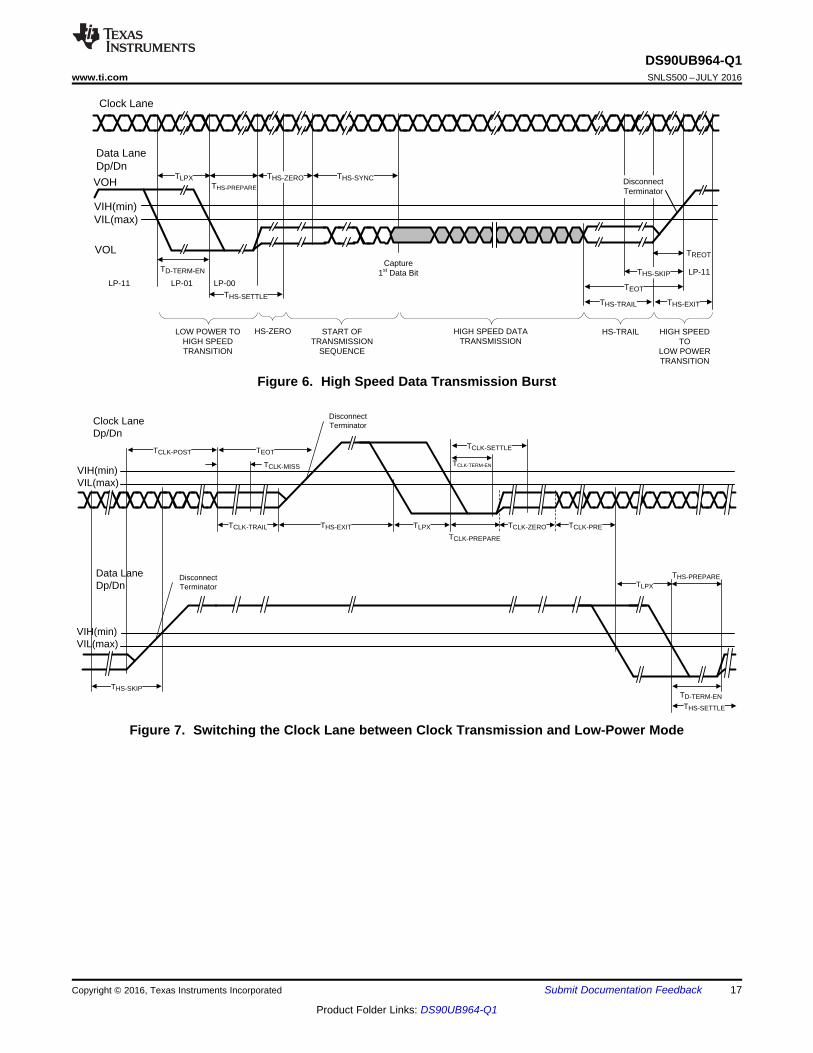
CSI-2 TIMING SPECIFICATIONS - GLOBAL OPERATION (Figure 6, Figure 7)
tCLK-MISS
Timeout for receiver to detectabsence of Clock transitionsand disable the Clock Lane HS-RX (1)
CSI0_D0P/NCSI0_D1P/NCSI0_D2P/NCSI0_D3P/NCSI1_D0P/NCSI1_D1P/NCSI1_D2P/NCSI1_D3P/NCSI0_CLKP/NCSI1_CLKP/N
60 ns
tCLK-POST HS exit (1)60 +
52×UIINST
ns
tCLK-PRE
Time HS clock shall be driverprior to any associated DataLane beginning the transitionfrom LP to HS mode (1)
8 UIINST
tCLK-PREPARE
Clock Lane HS Entry (1) 38 95 ns
tCLK-SETTLE
Time interval during which theHS receiver shall ignore anyClock Lane HS transitions (1)
95 300 ns
tCLK-TERM-EN
Time-out at Clock Lane DisplayModule to enable HSTermination (1)
Timefor Dn
to reachVTERM
-EN
38 ns
tCLK-TRAIL
Time that the transmitter drivesthe HS-0 state after the lastpayload clock bit of a HStransmission burst (1)
60 ns
tCLK-PREPARE +tCLK-ZERO
TCLK-PREPARE + time thatthe transmitter drives the HS-0state prior to starting theClock (1)
300 ns
tD-TERM-EN
Time for the Data Lane receiverto enable the HS linetermination (1)
Timefor Dn
to reachV-
TERM-EN
35 +4×UIINS
T
ns
tEOT
Transmitted time interval fromthe start of tHS-TRAIL to the startof the LP-11 state following aHS burst (1)
105 +12×UIIN
ST
ns
tHS-EXITTime that the transmitter drivesLP=11 following a HS burst (1) 100 ns
tHS-PREPARE Data Lane HS Entry (1)40 +
4×UIINST
85 +6×UIINS
T
ns
tHS-PREPARE+ tHS-ZERO
tHS-PREPARE + time that thetransmitter drives the HS-0state prior to transmitting theSync sequence (1)
145 +10×UIIN
ST
ns
tHS-SETTLE
Time interval during which theHS receiver shall ignore anyData Lane HS transitions,starting from the beginning oftHS-SETTLE
(1)
85 +6×UIINS
T
145 +10×UIIN
ST
ns
GPIOx (LOCK)
PDB=H
tDDLT
RIN±
VDDIO/2
VCM
GND
V+
V-
VID
80%
VDDIO
20%
tCLH tCHL
GND
15
DS90UB964-Q1www.ti.com SNLS500 –JULY 2016
Product Folder Links: DS90UB964-Q1
Submit Documentation FeedbackCopyright © 2016, Texas Instruments Incorporated
AC Electrical Characteristics (continued)Over recommended operating supply and temperature ranges unless otherwise specified.
PARAMETER TEST CONDITIONS PIN ORFREQUENCY MIN TYP MAX UNIT
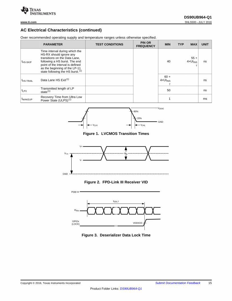
tHS-SKIP
Time interval during which theHS-RX should ignore anytransitions on the Data Lane,following a HS burst. The endpoint of the interval is definedas the beginning of the LP-11state following the HS burst. (1)
4055 +
4×UIINST
ns
tHS-TRAIL Data Lane HS Exit (1)60 +
4×UIINST
ns
tLPXTransmitted length of LPstate (1) 50 ns
tWAKEUPRecovery Time from Ultra LowPower State (ULPS) (1) 1 ms
Figure 1. LVCMOS Transition Times
Figure 2. FPD-Link III Receiver VID
Figure 3. Deserializer Data Lock Time

CSI[1:0]_CLKP
CSI[1:0]_CLKN
0.5UI + tSKEW
1 UI
CSI[1:0]_D[3:0]P
CSI[1:0]_D[3:0]N
SCL
SDA
tHD;STA
tLOW
tr
tHD;DAT
tHIGH
tf
tSU;DAT
tSU;STA tSU;STO
tf
START REPEATEDSTART
STOP
tHD;STA
START
trtBUF
16
DS90UB964-Q1SNLS500 –JULY 2016 www.ti.com
Product Folder Links: DS90UB964-Q1
Submit Documentation Feedback Copyright © 2016, Texas Instruments Incorporated
Figure 4. I2C Serial Control Bus Timing
Figure 5. Clock and Data Timing in HS Transmission
TCLK-POST
Clock LaneDp/Dn
VIH(min)VIL(max)
TEOT
THS-SKIP
Data LaneDp/Dn
TCLK-SETTLE
TCLK-TERM-EN
TCLK-TRAIL THS-EXIT TLPX TCLK-ZERO TCLK-PRE
THS-SETTLE
TLPX
VIH(min)VIL(max)
TCLK-MISS
Disconnect Terminator
Disconnect Terminator
TCLK-PREPARE
THS-PREPARE
TD-TERM-EN
TLPX
THS-SETTLETHS-TRAIL THS-EXIT
TEOT
THS-SKIP
THS-ZERO THS-SYNC
VIH(min)VIL(max)
Clock Lane
Data LaneDp/Dn
Disconnect Terminator
LP-11 LP-01 LP-00LP-11
Capture1st Data Bit
THS-PREPARE
TD-TERM-EN
TREOT
LOW POWER TO HIGH SPEED TRANSITION
HS-ZERO START OF TRANSMISSION
SEQUENCE
HIGH SPEED DATATRANSMISSION
HS-TRAIL HIGH SPEEDTO
LOW POWERTRANSITION
VOH
VOL
17
DS90UB964-Q1www.ti.com SNLS500 –JULY 2016
Product Folder Links: DS90UB964-Q1
Submit Documentation FeedbackCopyright © 2016, Texas Instruments Incorporated
Figure 6. High Speed Data Transmission Burst
Figure 7. Switching the Clock Lane between Clock Transmission and Low-Power Mode

FS
Pac
ket H
eade
r, P
H
Line Data
Pac
ket F
oote
r, P
F
FE
FS
Pac
ket H
eade
r, P
H
Line Data
Pac
ket F
oote
r, P
F
FE
(1 to N) tLPX
Line Blanking
Frame Blanking
Frame Blanking
Frame Blanking
Line Blanking
Vertical Blanking
VVALID(internal Node)
FE FSLPS
1 to 216 tLPX
HVALID(internal Node)
LPS
LinePacket
LinePacket
LPS LPS
LinePacket
LPS LPS LPS
1st
Line2nd
LineLastLine
CSI0_D[3:0]± or CSI1_D[3:0]±
LinePacket
LinePacket
SoT PH
EoT
Frame SyncPacket
FS
LPSS
oT
PH
PF
EoT
Line
Pix
elD
ata
18
DS90UB964-Q1SNLS500 –JULY 2016 www.ti.com
Product Folder Links: DS90UB964-Q1
Submit Documentation Feedback Copyright © 2016, Texas Instruments Incorporated
Figure 8. Long Line Packets and Short Frame Sync Packets
Figure 9. CSI-2 General Frame Format

CS
I-2
Out
put (
500
mV
/DIV
)
Time (50 ns/DIV)
CS
I-2
Out
put (
500
mV
/DIV
)
Time (50 ns/DIV)
LANE 0 SOT BYTE 0 BYTE 4 BYTE 8 BYTE n-4 EOT
LANE 1 SOT BYTE 1 BYTE 5 BYTE 9 BYTE n-3 EOT
LANE 2 SOT BYTE 2 BYTE 6 BYTE 10 BYTE n-2 EOT
LANE 3 SOT BYTE 3 BYTE 7 BYTE 11 BYTE n-1 EOT
HS BYTES TRANSMITTED (n) IS INTEGER MULTIPLE OF 4
LANE 0 SOT BYTE 0 BYTE 4 BYTE 8 BYTE n-3 EOT
LANE 1 SOT BYTE 1 BYTE 5 BYTE 9 BYTE n-2 EOT
LANE 2 SOT BYTE 2 BYTE 6 BYTE 10 BYTE n-1 EOT
LANE 3 SOT BYTE 3 BYTE 7 BYTE 11 EOT
HS BYTES TRANSMITTED (n) IS 1 LESS THAN INTEGER MULTIPLE OF 4
LANE 0 SOT BYTE 0 BYTE 4 BYTE 8 BYTE n-2 EOT
LANE 1 SOT BYTE 1 BYTE 5 BYTE 9 BYTE n-1 EOT
LANE 2 SOT BYTE 2 BYTE 6 BYTE 10 EOT
LANE 3 SOT BYTE 3 BYTE 7 BYTE 11 EOT
HS BYTES TRANSMITTED (n) IS 2 LESS THAN INTEGER MULTIPLE OF 4
LANE 0 SOT BYTE 0 BYTE 4 BYTE 8 BYTE n-1 EOT
LANE 1 SOT BYTE 1 BYTE 5 BYTE 9 EOT
LANE 2 SOT BYTE 2 BYTE 6 BYTE 10 EOT
LANE 3 SOT BYTE 3 BYTE 7 BYTE 11 EOT
HS BYTES TRANSMITTED (n) IS 3 LESS THAN INTEGER MULTIPLE OF 4
4 CSI-2 Data Lane Configuration (default)
LANE 0 SOT BYTE 0 BYTE 3 BYTE 6 BYTE n-3 EOT
LANE 1 SOT BYTE 1 BYTE 4 BYTE 7 BYTE n-2 EOT
LANE 2 SOT BYTE 2 BYTE 5 BYTE 8 BYTE n-1 EOT
HS BYTES TRANSMITTED (n) IS INTEGER MULTIPLE OF 3
LANE 0 SOT BYTE 0 BYTE 3 BYTE 6 BYTE n-2 EOT
LANE 1 SOT BYTE 1 BYTE 4 BYTE 7 BYTE n-1 EOT
LANE 2 SOT BYTE 2 BYTE 5 BYTE 8 EOT
HS BYTES TRANSMITTED (n) IS 1 LESS THAN INTEGER MULTIPLE OF 3
LANE 0 SOT BYTE 0 BYTE 3 BYTE 6 BYTE n-1 EOT
LANE 1 SOT BYTE 1 BYTE 4 BYTE 7 EOT
LANE 2 SOT BYTE 2 BYTE 5 BYTE 8 EOT
HS BYTES TRANSMITTED (n) IS 2 LESS THAN INTEGER MULTIPLE OF 3
3 CSI-2 Data Lane Configuration
LANE 0 SOT BYTE 0
BYTE 3
EOT
LANE 1 SOT BYTE 1
BYTE 4 BYTE n-2
EOT
HS BYTES TRANSMITTED (n) IS INTEGER MULTIPLE OF 2
LANE 0 SOT BYTE 0
BYTE 3
EOT
LANE 1 SOT BYTE 1
BYTE 4 BYTE n-1
EOT
HS BYTES TRANSMITTED (n) IS 1 LESS THAN INTEGER MULTIPLE OF 2
BYTE 2
BYTE 5 BYTE n-1
BYTE 2
BYTE 5
2 CSI-2 Data Lane Configuration
19
DS90UB964-Q1www.ti.com SNLS500 –JULY 2016
Product Folder Links: DS90UB964-Q1
Submit Documentation FeedbackCopyright © 2016, Texas Instruments Incorporated
Figure 10. 4 MIPI Data Lane Configuration
7 Typical Characteristics
Figure 11. CSI-2 Start of Transmission (SoT) Figure 12. CSI-2 End of Transmission (EoT)

PDB
DP
HY
Out
put
MIPI CSI-2Port 0
CLOCK MIPI CSI-2
Outputs
Clock Gen
CMLOUTPCMLOUTN
Timing and
Control
Lane
Man
agem
ent /
Des
kew
/ S
ync
I/F /
Mem
ory
I2C Controller
IDx
I2C_SDAI2C_SCL
GPIOs
Ser
ial t
o P
aral
lel
CD
R
Dec
oder
Virt
ual C
hann
el B
uffe
rs
CS
I-2
Pro
toco
l Int
erfa
ce
MIPI CSI-2Port 1
RIN0-
RIN0+
RIN1-
RIN1+
RIN2-
RIN2+
RIN3-
RIN3+
BC
CC
DR
BC
CC
DR
BC
CC
DR
BC
C
MODE
REFCLK
INTB
I2C_SDA2
I2C_SCL2
20
DS90UB964-Q1SNLS500 –JULY 2016 www.ti.com
Product Folder Links: DS90UB964-Q1
Submit Documentation Feedback Copyright © 2016, Texas Instruments Incorporated
8 Detailed Description
8.1 OverviewThe DS90UB964-Q1 is a camera hub that accepts four camera inputs from a FPD-Link III interface. The devicecombines data streams from multiple camera sources onto one or two MIPI CSI-2 port(s) with up to 4 data laneseach port.
8.2 Functional Block DiagramThe DS90UB964-Q1 is a camera hub that aggregates up to four inputs acquired from a FPD-Link III stream andtransmitted over a MIPI camera serial interface (CSI-2). When coupled with DS90UB913AQ/913Q/933Q FPD-Link III serializers, the DS90UB964-Q1 receives data streams from multiple imagers to be multiplexed on thesame CSI-2 links.
The DS90UB964-Q1 provides two MIPI CSI-2 ports, configuration with 4 lanes per port up to 1.6 Gbps per lane.The second MIPI CSI-2 output port is available to provide additional bandwidth, or offers a second replicatedoutput. The DS90UB964-Q1 can support multiple data formats (programmable as RAW, YUV, RGB) anddifferent camera resolutions. The CSI-2 Tx module accommodates both image data and non-image data(including synchronization or embedded data packets).
The DS90UB964-Q1 CSI-2 interface combines each of the camera data streams into packets designated foreach virtual channel. The output generated is composed of virtual channels to separate different streams to beinterleaved. Each virtual channel is identified by a unique channel identification number in the packet header.
Figure 13. Functional Block Diagram
8.3 Feature DescriptionThe DS90UB964-Q1 provides a 4:2 hub for camera applications. The device includes 4 FPD-Link III inputs forcamera data streams from up to 4 serializers. The interfaces are compatible to DS90UB913AQ/913Q/933Qserializers. Data received from the 4 input ports is aggregated onto one or two 4-lane CSI-2 interfaces.
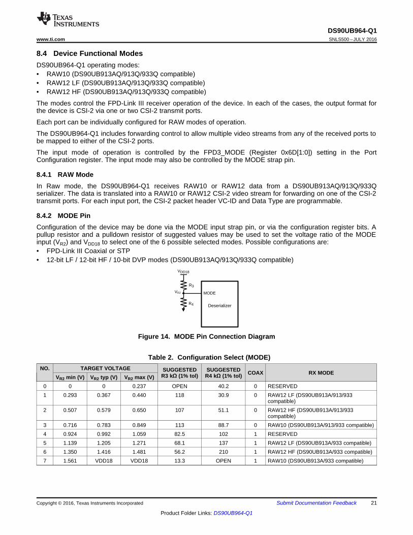
DeserializerR4
MODE
VDD18
R3
VR2
21
DS90UB964-Q1www.ti.com SNLS500 –JULY 2016
Product Folder Links: DS90UB964-Q1
Submit Documentation FeedbackCopyright © 2016, Texas Instruments Incorporated
8.4 Device Functional ModesDS90UB964-Q1 operating modes:• RAW10 (DS90UB913AQ/913Q/933Q compatible)• RAW12 LF (DS90UB913AQ/913Q/933Q compatible)• RAW12 HF (DS90UB913AQ/913Q/933Q compatible)
The modes control the FPD-Link III receiver operation of the device. In each of the cases, the output format forthe device is CSI-2 via one or two CSI-2 transmit ports.
Each port can be individually configured for RAW modes of operation.
The DS90UB964-Q1 includes forwarding control to allow multiple video streams from any of the received ports tobe mapped to either of the CSI-2 ports.
The input mode of operation is controlled by the FPD3_MODE (Register 0x6D[1:0]) setting in the PortConfiguration register. The input mode may also be controlled by the MODE strap pin.
8.4.1 RAW ModeIn Raw mode, the DS90UB964-Q1 receives RAW10 or RAW12 data from a DS90UB913AQ/913Q/933Qserializer. The data is translated into a RAW10 or RAW12 CSI-2 video stream for forwarding on one of the CSI-2transmit ports. For each input port, the CSI-2 packet header VC-ID and Data Type are programmable.
8.4.2 MODE PinConfiguration of the device may be done via the MODE input strap pin, or via the configuration register bits. Apullup resistor and a pulldown resistor of suggested values may be used to set the voltage ratio of the MODEinput (VR2) and VDD18 to select one of the 6 possible selected modes. Possible configurations are:• FPD-Link III Coaxial or STP• 12-bit LF / 12-bit HF / 10-bit DVP modes (DS90UB913AQ/913Q/933Q compatible)
Figure 14. MODE Pin Connection Diagram
Table 2. Configuration Select (MODE)NO. TARGET VOLTAGE SUGGESTED
R3 kΩ (1% tol)SUGGESTED
R4 kΩ (1% tol) COAX RX MODEVR2 min (V) VR2 typ (V) VR2 max (V)
0 0 0 0.237 OPEN 40.2 0 RESERVED1 0.293 0.367 0.440 118 30.9 0 RAW12 LF (DS90UB913A/913/933
compatible)2 0.507 0.579 0.650 107 51.1 0 RAW12 HF (DS90UB913A/913/933
compatible)3 0.716 0.783 0.849 113 88.7 0 RAW10 (DS90UB913A/913/933 compatible)4 0.924 0.992 1.059 82.5 102 1 RESERVED5 1.139 1.205 1.271 68.1 137 1 RAW12 LF (DS90UB913A/933 compatible)6 1.350 1.416 1.481 56.2 210 1 RAW12 HF (DS90UB913A/933 compatible)7 1.561 VDD18 VDD18 13.3 OPEN 1 RAW10 (DS90UB913A/933 compatible)

Amplitude(UI p-p)
g (MHz)
A1
A2
g1 g2
22
DS90UB964-Q1SNLS500 –JULY 2016 www.ti.com
Product Folder Links: DS90UB964-Q1
Submit Documentation Feedback Copyright © 2016, Texas Instruments Incorporated
The strapped values can be viewed and/or modified in the following locations:• Coaxial – Port Configuration COAX_MODE (Register 0x6D[2])• RX Mode – Port Configuration FPD3_MODE (Register 0x6D[1:0])
8.4.3 REFCLKA valid 25 MHz (default) reference clock is required on the REFCLK pin 5 for proper operation. REFCLK inputmust be continuous. The REFCLK frequency defines all internal clock timers including the back channel rate, I2Ctimers, CSI-2 datarate, FrameSync signal parameters, etc. Min stop time (stop at high or stop at low) is 20 uS,otherwise it is required to reset using PDB. During normal operation if REFCLK input is removed and then re-applied this may cause CSI-2 output to be disrupted.
The REFCLK LVCMOS input oscillator specifications are listed in Table 3.
Table 3. REFCLK Oscillator SpecificationsPARAMETER TEST CONDITIONS MIN TYP MAX UNIT
REFERENCE CLOCKFrequency tolerance ±100 ppmDuty cycle 40% 50% 60%Rise/Fall Time 10% - 90% 8 nsJitter 500 kHz - 50 MHz 50 80 ps p-pFrequency 23 25 MHz
(1) FPD3_PCLK is equivalent to PCLK frequency based on the operating MODE:10-bit mode: PCLK_Freq. /212-bit HF mode: PCLK_Freq. x 2/312-bit LF mode: PCLK_Freq.
8.4.4 Input Jitter ToleranceInput jitter tolerance is the ability of the receiver's CDR PLL to track and recover the incoming serial data stream.Jitter tolerance at a specific frequency is the maximum jitter permissible before data errors occur. The followingshows the allowable total jitter of the receiver inputs and must be less than the values in the chart.
Figure 15. Input Jitter Tolerance Plot
Table 4. Input Jitter Tolerance LimitINTERFACE JITTER AMPLITUDE (UI p-p) FREQUENCY (MHz) (1)
FPD3A1 A2 ƒ1 ƒ21 0.4 FPD3_PCLK / 80 FPD3_PCLK / 15

VOD (+)
tBIT (1 UI)
Ew
VOD (-)
0V
23
DS90UB964-Q1www.ti.com SNLS500 –JULY 2016
Product Folder Links: DS90UB964-Q1
Submit Documentation FeedbackCopyright © 2016, Texas Instruments Incorporated
(1) UI – Unit Interval is equivalent to one ideal serialized data bit width. The UI scales with serializer input PCLK frequency.10-bit mode: 1 UI = 1 / ( PCLK_Freq. /2 x 28 )12-bit HF mode: 1 UI = 1 / ( PCLK_Freq. x 2/3 x 28 )12-bit LF mode: 1 UI = 1 / ( PCLK_Freq. x 28 )
8.4.5 Adaptive EqualizerThe receiver inputs provide an adaptive equalization filter in order to compensate for signal degradation from theinterconnect components. In order to determine the maximum cable reach, factors that affect signal integrity suchas jitter, skew, ISI, crosstalk, etc. need to be taken into consideration. The equalization status and configurationare selected via AEQ registers 0xD2–0xD5.
Each RX receiver incorporates an adaptive equalizer (AEQ), which continuously monitors cable characteristicsfor long-term cable aging and temperature changes. The AEQ attempts to optimize the equalization setting of theRX receiver.
If the deserializer loses LOCK, the adaptive equalizer will reset and perform the LOCK algorithm again toreacquire the serial data stream being sent by the serializer.
8.4.6 Channel Monitor Loop-Through Output DriverThe DS90UB964-Q1 includes an internal Channel Monitor Loop-through output on the CMLOUTP/N pins. Abuffered loop-through output driver is provided on the CMLOUTP/N for observing jitter after equalization for eachof the four RX receive channels. The CMLOUT monitors the post EQ stage thus providing the recovered input ofthe deserializer signal. The measured serial data width on the CMLOUT loop-through is the total jitter includingthe internal driver, AEQ, back channel echo, etc. Each channel also has its own CMLOUT monitor and can beused for debug purposes. This CMLOUT is useful in identifying gross signal conditioning issues.
Table 6 includes details on selecting the corresponding RX receiver of CMLOUTP/N configuration.
Table 5. CML Monitor Output DriverPARAMETER TEST CONDITIONS PIN MIN TYP MAX UNIT
EWDifferential Output EyeOpening
RL = 100 Ω(Figure 16)
CMLOUTP,CMLOUTN 0.45 UI (1)
Figure 16. CMLOUT Output Driver
Table 6. Channel Monitor Loop-Through Output ConfigurationFPD3 RX Port 0 FPD3 RX Port 1 FPD3 RX Port 2 FPD3 RX Port 3
ENABLE MAIN LOOPTHRU DRIVER0xB0 = 0x140xB1 = 0x000xB2 = 0x80
0xB0 = 0x140xB1 = 0x000xB2 = 0x80
0xB0 = 0x140xB1 = 0x000xB2 = 0x80
0xB0 = 0x140xB1 = 0x000xB2 = 0x80
SELECT CHANNEL MUX 0xB1 = 0x010xB2 = 0x01
0xB1 = 0x010xB2 = 0x02
0xB1 = 0x010xB2 = 0x04
0xB1 = 0x010xB2 = 0x08
SELECT RX PORT
0xB0 = 0x040xB1 = 0x0F0xB2 = 0x010xB1 = 0x100xB2 = 0x02
0xB0 = 0x080xB1 = 0x0F0xB2 = 0x010xB1 = 0x100xB2 = 0x02
0xB0 = 0x0C0xB1 = 0x0F0xB2 = 0x010xB1 = 0x100xB2 = 0x02
0xB0 = 0x100xB1 = 0x0F0xB2 = 0x010xB1 = 0x100xB2 = 0x02

24
DS90UB964-Q1SNLS500 –JULY 2016 www.ti.com
Product Folder Links: DS90UB964-Q1
Submit Documentation Feedback Copyright © 2016, Texas Instruments Incorporated
8.4.6.1 Code Example for CMLOUT FPD3 RX Port 0:WriteI2C(0xB0,0x14) # FPD3 RX Shared, page 0WriteI2C(0xB1,0x00) # Offset 0 (reg_0_sh)WriteI2C(0xB2,0x80) # Enable loop throu driverWriteI2C(0xB1,0x01) # Select Drive MuxWriteI2C(0xB2,0x01) #WriteI2C(0xB0,0x04) # FPD3 RX Port 0, page 0WriteI2C(0xB1,0x0F) #WriteI2C(0xB2,0x01) # Loop through selectWriteI2C(0xB1,0x10) #WriteI2C(0xB2,0x02) # Enable CML data output
8.4.7 GPIO SupportThe DS90UB964-Q1 supports 8 pins which are programmable for use in multiple options through theGPIOx_PIN_CTL registers.
8.4.7.1 Back Channel GPIOThe DS90UB964-Q1 can input data on the GPIO pins to send on the back channel to remote serializers. EachGPIO pin can be programmed for input mode. In addition, the back channel for each FPD3 port can beprogrammed to send any of the 8 GPIO pin data. The same GPIO pin can be connected to multiple back channelGPIO signals.
In addition to sending GPIO from pins, an internally generated FrameSync signal may be sent on any of theback-channel GPIOs.
For each port, the following GPIO control is available through the BC_GPIO_CTL0 register 0x6E andBC_GPIO_CTL1 register 0x6F.
8.4.7.2 GPIO Pin StatusGPIO pin status may be read through the GPIO_PIN_STS register 0x0E. This register provides the status of theGPIO pin independent of whether the GPIO pin is configured as an input or output.
8.4.7.3 Other GPIO Pin ControlsEach GPIO pin can has a input disable and a pulldown disable. By default, the GPIO pin input paths are enabledand the internal pulldown circuit in the GPIO is enabled. The GPIO_INPUT_CTL register 0x0F andGPIO_PD_CTL register 0xBE allow control of the input enable and the pulldown respectively. For mostapplications, there is no need to modify the default register settings.
8.4.8 RAW Mode LV/FV ControlsThe Raw modes provide FrameValid (FV) and LineValid (LV) controls for the video framing. The FV is equivalentto a Vertical Sync (VSYNC) while the LineValid is equivalent to a Horizontal Sync (HSYNC) input to theDS90UB913AQ/913Q/933Q device.
The DS90UB964-Q1 allows setting the polarity of these signals by register programming. The FV and LV polarityare controlled on a per-port basis and can be independently set in the PORT_CONFIG2 register 0x7C.
To prevent false detection of FrameValid, FV must be asserted for a minimum number of clocks prior to firstvideo line to be considered valid. The minimum FrameValid time is programmable in the FV_MIN_TIME register0xBC. Since the measurement is in FPD3 clocks, the minimum FrameValid setup to LineValid timing at theSerializer will vary based on operating mode.
A minimum FV to LV timing is required when processing video frames at the serializer input. If the FV to LVminimum setup is not met (by default), the first video line is discarded. Optionally, a register control(PORT_CONFIG:DISCARD_1ST_ON_ERR) forwards the first video line missing some number of pixels at thestart of the line.

KEY:ST ± Start of Transmission PH ± Packet HeaderET ± End of Transmission PF ± Packet FooterLPS ± Low Power State
DATA:
DATA DATAPFPH PH PFSP SPLPSET ST LPSET STST LPSET ST ET
Short Packet
Long Packet
Long Packet
Short Packet
FV
LV
TFV_LV
§
25
DS90UB964-Q1www.ti.com SNLS500 –JULY 2016
Product Folder Links: DS90UB964-Q1
Submit Documentation FeedbackCopyright © 2016, Texas Instruments Incorporated
Figure 17. Minimum FV to LV
Table 7. Minimum FV to LV Setup Requirement (in Serializer PCLKs)
MODE FV_MIN_TIMEConversion Factor
Absolute Min(FV_MIN_TIME = 0)
Default(FV_MIN_TIME = 128)
RAW12 LF 1 2 130RAW12 HF 1.5 3 195
RAW10 2 5 261
For other settings of FV_MIN_TIME, the required FV to LV setup in Serializer PCLKs can be determined by:Absolute Min + (FV_MIN_TIME * Conversion factor)
8.4.9 CSI-2 Protocol LayerThe DS90UB964-Q1 implements High-Speed mode to forward CSI-2 Low Level Protocol data. This includesfeatures as described in the Low Level Protocol section of the MIPI CSI-2 Specification. It supports short andlong packet formats.
The feature set of the protocol layer implemented by the CSI-2 TX is:• Transport of arbitrary data (payload-independent)• 8-bit word size• Support for up to four interleaved virtual channels on the same link• Special packets for frame start, frame end, line start and line end information• Descriptor for the type, pixel depth and format of the Application Specific Payload data• 16-bit Checksum Code for error detection
Figure 18 shows the CSI-2 protocol layer with short and long packets.
Figure 18. CSI-2 Protocol Layer With Short and Long Packets
8.4.10 CSI-2 Short PacketThe short packet provides frame or line synchronization. Figure 19 shows the structure of a short packet. A shortpacket is identified by data types 0x00 to 0x0F.
16-B
itW
ord
Cou
nt
EC
C
Dat
a ID
Dat
a 0
Dat
a 1
Dat
a 2
Dat
a 3
Dat
a W
C-4
Dat
a W
C-3
Dat
a W
C-2
Dat
a W
C-1
16-b
it C
heck
sum
32-bit PACKET HEADER
(PH)
16-bit PACKET FOOTER
(PF)
PACKET DATA:Length = Word Count (WC) * Data Word Width (8-bits). There are NO restrictions on the values of the data words
16-B
itS
hort
Pac
ket
Dat
a F
ield
VC
X +
EC
C
Dat
a ID
32-bit SHORT PACKET (SH)Data Type (DT) = 0x00 ± 0x0F
26
DS90UB964-Q1SNLS500 –JULY 2016 www.ti.com
Product Folder Links: DS90UB964-Q1
Submit Documentation Feedback Copyright © 2016, Texas Instruments Incorporated
Figure 19. CSI-2 Short Packet Structure
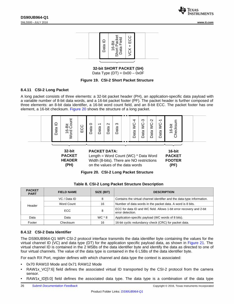
8.4.11 CSI-2 Long PacketA long packet consists of three elements: a 32-bit packet header (PH), an application-specific data payload witha variable number of 8-bit data words, and a 16-bit packet footer (PF). The packet header is further composed ofthree elements: an 8-bit data identifier, a 16-bit word count field, and an 8-bit ECC. The packet footer has oneelement, a 16-bit checksum. Figure 20 shows the structure of a long packet.
Figure 20. CSI-2 Long Packet Structure
Table 8. CSI-2 Long Packet Structure DescriptionPACKET
PART FIELD NAME SIZE (BIT) DESCRIPTION
Header
VC / Data ID 8 Contains the virtual channel identifier and the data-type information.Word Count 16 Number of data words in the packet data. A word is 8 bits.
ECC 8 ECC for data ID and WC field. Allows 1-bit error recovery and 2-biterror detection.
Data Data WC * 8 Application-specific payload (WC words of 8 bits).Footer Checksum 16 16-bit cyclic redundancy check (CRC) for packet data.
8.4.12 CSI-2 Data IdentifierThe DS90UB964-Q1 MIPI CSI-2 protocol interface transmits the data identifier byte containing the values for thevirtual channel ID (VC) and data type (DT) for the application specific payload data, as shown in Figure 21. Thevirtual channel ID is contained in the 2 MSBs of the data identifier byte and identify the data as directed to one offour virtual channels. The value of the data type is contained in the 6 LSBs of the data identifier byte.
For each RX Port, register defines with which channel and data type the context is associated:
• 0x70 RAW10 Mode and 0x71 RAW12 Mode• RAW1x_VC[7:6] field defines the associated virtual ID transported by the CSI-2 protocol from the camera
sensor.• RAW1x_ID[5:0] field defines the associated data type. The data type is a combination of the data type
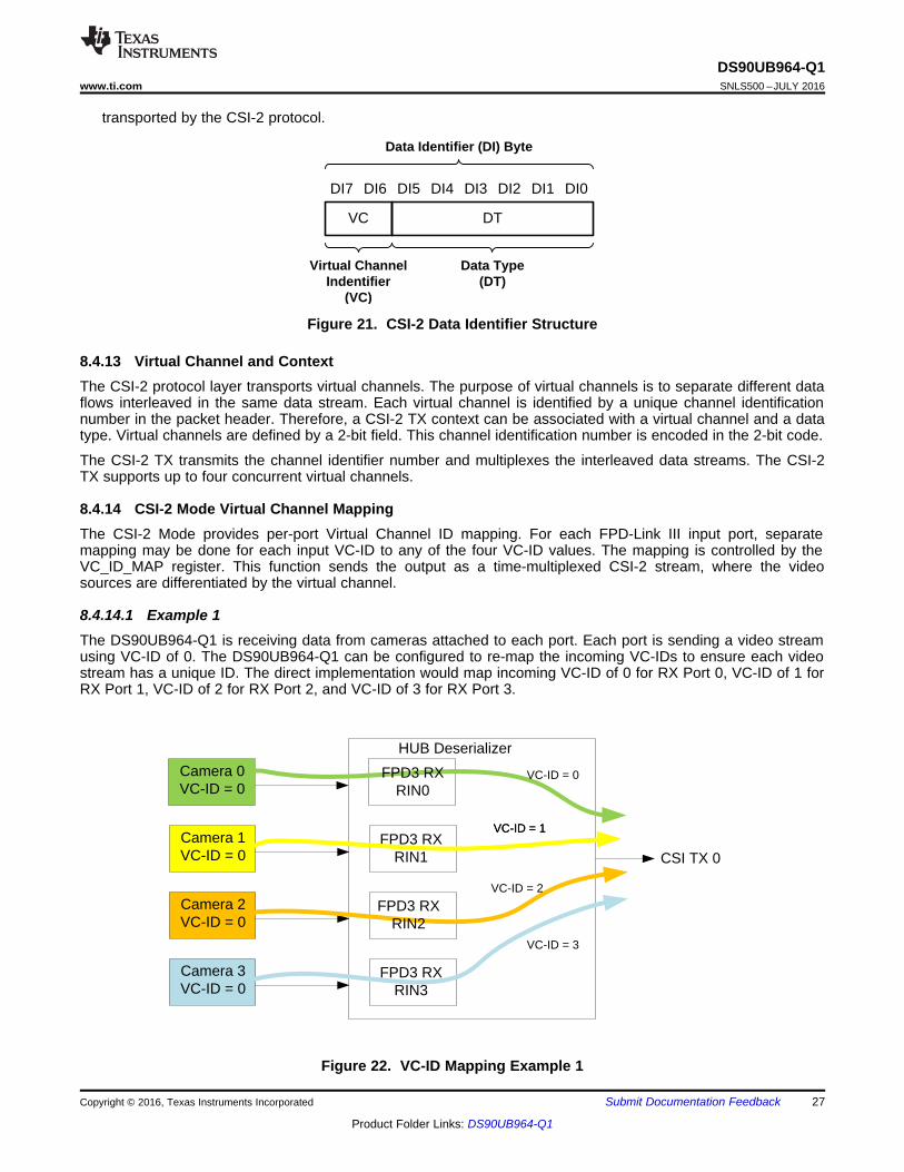
Camera 0VC-ID = 0
HUB Deserializer
CSI TX 0Camera 1VC-ID = 0
Camera 2VC-ID = 0
Camera 3VC-ID = 0
VC-ID = 0FPD3 RXRIN0
FPD3 RXRIN1
FPD3 RXRIN2
FPD3 RXRIN3
VC-ID = 1VC-ID = 1
VC-ID = 2
VC-ID = 3
VC
Virtual Channel Indentifier
(VC)
Data Type (DT)
Data Identifier (DI) Byte
DI7 DI4 DI3 DI0DI6 DI5 DI1DI2
DT
27
DS90UB964-Q1www.ti.com SNLS500 –JULY 2016
Product Folder Links: DS90UB964-Q1
Submit Documentation FeedbackCopyright © 2016, Texas Instruments Incorporated
transported by the CSI-2 protocol.
Figure 21. CSI-2 Data Identifier Structure
8.4.13 Virtual Channel and ContextThe CSI-2 protocol layer transports virtual channels. The purpose of virtual channels is to separate different dataflows interleaved in the same data stream. Each virtual channel is identified by a unique channel identificationnumber in the packet header. Therefore, a CSI-2 TX context can be associated with a virtual channel and a datatype. Virtual channels are defined by a 2-bit field. This channel identification number is encoded in the 2-bit code.
The CSI-2 TX transmits the channel identifier number and multiplexes the interleaved data streams. The CSI-2TX supports up to four concurrent virtual channels.
8.4.14 CSI-2 Mode Virtual Channel MappingThe CSI-2 Mode provides per-port Virtual Channel ID mapping. For each FPD-Link III input port, separatemapping may be done for each input VC-ID to any of the four VC-ID values. The mapping is controlled by theVC_ID_MAP register. This function sends the output as a time-multiplexed CSI-2 stream, where the videosources are differentiated by the virtual channel.
8.4.14.1 Example 1The DS90UB964-Q1 is receiving data from cameras attached to each port. Each port is sending a video streamusing VC-ID of 0. The DS90UB964-Q1 can be configured to re-map the incoming VC-IDs to ensure each videostream has a unique ID. The direct implementation would map incoming VC-ID of 0 for RX Port 0, VC-ID of 1 forRX Port 1, VC-ID of 2 for RX Port 2, and VC-ID of 3 for RX Port 3.
Figure 22. VC-ID Mapping Example 1

HUB Deserializer
FPD-Link III Serializer
FPD-Link III Serializer
FPD-Link III Serializer
FPD-Link III Serializer
A1
B1
A3
B3
A2
B2
A4Camera A
Camera B
C1 C3C2 C4Camera C
D1 D3D2 D4Camera D
CS
I-2
Por
t0C
SI-
2 P
ort1
LP11
LP11
LP11A1 B1 C1
LP11
LP11
LP11A2 B2 C2
LP11
LP11 A3 B3 C3
LP11
LP11 A4 B4
Color of the packet represents the VC-ID
B4
D1 D2
LP11
LP11
LP11
LP11D3 C4
LP11 D4
CSI-2 port0, 1 CK lane, up to 4 data lanes
Camera 0VC-ID = 0
HUB Deserializer
CSI TX 0Camera 1VC-ID = 0
Camera 2VC-ID = 0
Camera 3VC-ID = 0
VC-ID = 0FPD3 RXRIN0
FPD3 RXRIN1
FPD3 RXRIN2
FPD3 RXRIN3
VC-ID = 1
VC-ID = 0
VC-ID = 1
CSI TX 1
28
DS90UB964-Q1SNLS500 –JULY 2016 www.ti.com
Product Folder Links: DS90UB964-Q1
Submit Documentation Feedback Copyright © 2016, Texas Instruments Incorporated
8.4.14.2 Example 2The DS90UB964-Q1 is receiving data from cameras attached to each port. Each port is sending a video streamusing VC-ID of 0. The DS90UB964-Q1 can be configured to re-map the incoming VC-IDs and distribute todifferent CSI Transmitters. This implementation maps incoming VC-ID of 0 for RX Port 0, VC-ID of 1 for RX Port1, VC-ID of 0 for RX Port 2, and VC-ID of 1 for RX Port 3. RX Ports 0 and 1 are assigned to CSI Transmitter 0which RX Ports 2 and 3 are assigned to CSI Transmitter 1.
Figure 23. VC-ID Mapping Example 2
Figure 24. Four Camera Data onto CSI-2 With Virtual Channels (VC-ID)

HUBDeserializer
FPD-Link III Serializer
FPD-Link III Serializer
FPD-Link III Serializer
FPD-Link III Serializer
A1
B1
A3
B3
A2
B2
A4Camera A
Camera B
C1 C3C2 C4Camera C
D1 D2Camera D
CS
I-2
Por
t0C
SI-
2 P
ort1
LP11
LP11
LP11A1 B1 C1
LP11
LP11
LP11A2 B2 C2
LP11
LP11 A3 B3 C3
LP11
LP11 A4D1 D2
LP11
LP11 C4
CSI-2 port0, 1 CK lane, up to 4 data lanes
LP11
LP11
LP11A1 B1 C1
LP11
LP11
LP11A2 B2 C2
LP11
LP11 A3 B3 C3
LP11
LP11 A4D1 D2
LP11
LP11 C4
CSI-2 port1, 1 CK lane, up to 4 data lanes
Port1 can be the Replica of Port0
Camera B and Camera D have less packets
HUBDeserializer
FPD-Link III Serializer
FPD-Link III Serializer
FPD-Link III Serializer
FPD-Link III Serializer
A1
B1
A3
B3
A2
B2
A4Camera A
Camera B
C1 C3C2 C4Camera C
D1 D3D2 D4Camera D
CS
I-2
Por
t0C
SI-
2 P
ort1
LP11
LP11
LP11A1 B1 C1
LP11
LP11
LP11A2 B2 C2
LP11
LP11A3 B3 C3
LP11
LP11A4 C4
LP11
LP11
LP11D1 D2 D3 D4
Color of the packet represents the VC-ID
Each CSI-2 port can carry data from 1,2,3, or all cameras, depending on bandwidth
CAM B has less packets (because CAM A and CAM C & D have, e.g. embedded data)
CSI-2 port0, 1 CK lane, up to 4 data lanes
CSI-2 port1, 1 CK lane, up to 4 data lanes
Not shown:One FS packetfor each VC-ID
29
DS90UB964-Q1www.ti.com SNLS500 –JULY 2016
Product Folder Links: DS90UB964-Q1
Submit Documentation FeedbackCopyright © 2016, Texas Instruments Incorporated
Figure 25. Four Camera Data onto CSI-2 With Virtual Channels (VC-ID) With Different Frame Size
Figure 26. Four Camera Data onto 1xCSI-2 Replicated With Virtual Channels (VC-ID) With Different FrameSize
8.4.15 CSI-2 Transmitter FrequencyThe CSI-2 Transmitters may operate at 400 or 800 Mbps or 1.6 Gbps. This operation is controlled via theCSI_PLL_CTL 0x1F register.
CSI_PLL_CTL[1:0] CSI-2 TX Frequency REFCLK Frequency
001.6 Gbps 25 MHz
1.472 Gbps 23 MHz01 Reserved Reserved10 800 Mbps 25 MHz11 400 Mbps 25 MHz
When configuring to 800 Mbps or 1.6 Gbps, the CSI-2 timing parameters are automatically set based on theCSI_PLL_CTL 0x1F register. In the case of 400 Mbps, the respective CSI-2 timing parameters registers must beprogrammed, and the appropriate override bit needs to be set. To enable CSI-2 400 Mbps mode, set thefollowing registers:
# Set CSI Timing parametersWriteI2C(0xB0,0x2) # set auto-increment, page 0WriteI2C(0xB1,0x40) # CSI Port 0

30
DS90UB964-Q1SNLS500 –JULY 2016 www.ti.com
Product Folder Links: DS90UB964-Q1
Submit Documentation Feedback Copyright © 2016, Texas Instruments Incorporated
WriteI2C(0xB2,0x83) # TCK PrepWriteI2C(0xB2,0x8D) # TCK ZeroWriteI2C(0xB2,0x87) # TCK TrailWriteI2C(0xB2,0x87) # TCK PostWriteI2C(0xB2,0x83) # THS PrepWriteI2C(0xB2,0x86) # THS ZeroWriteI2C(0xB2,0x84) # THS TrailWriteI2C(0xB2,0x86) # THS ExitWriteI2C(0xB2,0x84) # TLPX
# Set CSI Timing parametersWriteI2C(0xB0,0x2) # set auto-increment, page 0WriteI2C(0xB1,0x60) # CSI Port 1WriteI2C(0xB2,0x83) # TCK PrepWriteI2C(0xB2,0x8D) # TCK ZeroWriteI2C(0xB2,0x87) # TCK TrailWriteI2C(0xB2,0x87) # TCK PostWriteI2C(0xB2,0x83) # THS PrepWriteI2C(0xB2,0x86) # THS ZeroWriteI2C(0xB2,0x84) # THS TrailWriteI2C(0xB2,0x86) # THS ExitWriteI2C(0xB2,0x84) # TLPX
8.4.16 Video BuffersThe DS90UB964-Q1 implements four video line buffer/FIFO, one for each RX channel. The video buffers providestorage of data payload and forward requirements for sending multiple video streams on the CSI-2 transmitports. The total line buffer memory size is a 16-kB block for each RX port.
The CSI-2 transmitter waits for an entire packet to be available before pulling data from the video buffers.
8.4.17 CSI-2 Line Count and Line LengthThe DS90UB964-Q1 counts the number of lines (long packets) to determine line count on LINE_COUNT_1/0registers 0x73–74. For line length, DS90UB964-Q1 generates the word count field in the CSI-2 header onLINE_LEN_1/0 registers 0x75–0x76.
8.4.18 FrameSync OperationA frame synchronization signal (FrameSync) can be sent via the back-channel using any of the back channelGPIOs. The signal can be generated in two different methods. The first option offers sending the externalFrameSync using one of the available GPIO pins on the DS90UB964-Q1 and mapping that GPIO to a backchannel GPIO on one or more of the FPD-Link III ports.
The second option is to have the DS90UB964-Q1 internally generate a FrameSync signal to send via GPIO toone or more of the attached Serializers.
FrameSync signaling on the four back channels is synchronous. Thus, the FrameSync signal arrives at each ofthe four serializers with limited skew.
8.4.18.1 External FrameSync ControlIn External FrameSync mode, an external signal is input to the DS90UB964-Q1 via one of the GPIO pins on thedevice. The external FrameSync signal may be propagated to one or more of the attached FPD3 Serializers viaa GPIO signal in the back channel.

HUB Deserializer
SerializerGPIOx
BC_GPIOx
BC_GPIOx
BC_GPIOx
BC_GPIOxSerializerGPIOx
SerializerGPIOx
SerializerGPIOx
FPD-Link III
FPD-Link III
FPD-Link III
FPD-Link IIIGPIOy
31
DS90UB964-Q1www.ti.com SNLS500 –JULY 2016
Product Folder Links: DS90UB964-Q1
Submit Documentation FeedbackCopyright © 2016, Texas Instruments Incorporated
Figure 27. External FrameSync
Enabling the external FrameSync mode is done by setting the FS_MODE control in the FS_CTL register to avalue between 0x8 (GPIO0 pin) to 0xF (GPIO7 pin). Set FS_GEN_ENABLE to 0 for this mode.
To send the FrameSync signal on a port’s BC_GPIOx signal, the BC_GPIO_CTL0 or BC_GPIO_CTL1 registershould be programmed for that port to select the FrameSync signal.
8.4.18.2 Internally Generated FrameSyncIn Internal FrameSync mode, an internally generated FrameSync signal is sent to one or more of the attachedFPD3 Serializers via a GPIO signal in the back channel.
FrameSync operation is controlled by the FS_CTL 0x18, FS_HIGH_TIME_x, and FS_LOW_TIME_x 0x19–0x1Aregisters. The resolution of the FrameSync generator clock (FS_CLK_PD) is derived from the back channelframe period (BC_FREQ_SELECT register). For each 2.5 Mbps back-channel , the frame period is 12 µs (30 bits* 400 ns/bit).
Once enabled, the FrameSync signal is sent continuously based on the programmed conditions.
Enabling the internal FrameSync mode is done by setting the FS_GEN_ENABLE control in the FS_CTL registerto a value of 1. The FS_MODE field controls the clock source used for the FrameSync generation. TheFS_GEN_MODE field configures whether the duty cycle of the FrameSync is 50/50 or whether the high and lowperiods are controlled separately. The FrameSync high and low periods are controlled by the FS_HIGH_TIMEand FS_LOW_TIME registers.
The accuracy of the internally generated FrameSync is directly dependent on the accuracy of the 25 MHzoscillator used as the reference clock.

FS_HIGH FS_LOW
FS_LOW = FS_LOW_TIME * FS_CLK_PDFS_HIGH = FS_HIGH_TIME * FS_CLK_PDwhere FS_CLK_PD is the resolution of the FrameSync generator clock
HUB Deserializer
SerializerGPIOx FrameSync
GeneratorBC_GPIOx
BC_GPIOx
BC_GPIOx
BC_GPIOxSerializerGPIOx
SerializerGPIOx
SerializerGPIOx
FPD-Link III
FPD-Link III
FPD-Link III
FPD-Link III
32
DS90UB964-Q1SNLS500 –JULY 2016 www.ti.com
Product Folder Links: DS90UB964-Q1
Submit Documentation Feedback Copyright © 2016, Texas Instruments Incorporated
Figure 28. Internal FrameSync
Figure 29. Internal FrameSync Signal
The following example shows generation of a FrameSync signal at 60 pulses per second. Mode settings:• Programmable High/Low periods: FS_GEN_MODE 0x18[1]=0• Use port 0 back channel frame period: FS_MODE 0x18[7:4]=0x0• Back channel rate of 2.5 Mbps: BC_FREQ_SELECT for port 0 0x58[2:0]=0x0• Initial FS state of 0: FS_INIT_STATE 0x18[2]=0
Based on mode settings, the FrameSync is generated based upon FS_CLK_PD of 12 us.
The total period of the FrameSync is (1 sec / 60 hz) / 12 µs or approximately 1,389 counts.
For a 10% duty cycle, set the high time to 139 (0x008A) cycles, and the low time to 1,250 (0x04E1) cycles:• FS_HIGH_TIME_1: 0x19=0x00• FS_HIGH_TIME_0: 0x1A=0x8A• FS_LOW_TIME_1: 0x1B=0x04• FS_LOW_TIME_0: 0x1C=0xE1
8.4.18.2.1 Code Example for Internally Generated FrameSyncWriteI2C(0x4C,0x01) # RX0WriteI2C(0x6E,0xAA) # BC_GPIO_CTL0: FrameSync signal to GPIO0/1WriteI2C(0x4C,0x12) # RX1WriteI2C(0x6E,0xAA) # BC_GPIO_CTL0: FrameSync signal to GPIO0/1WriteI2C(0x4C,0x24) # RX2WriteI2C(0x6E,0xAA) # BC_GPIO_CTL0: FrameSync signal to GPIO0/1WriteI2C(0x4C,0x38) # RX3WriteI2C(0x6E,0xAA) # BC_GPIO_CTL0: FrameSync signal to GPIO0/1WriteI2C(0x10,0x91) # FrameSync signal; Device Status; EnabledWriteI2C(0x58,0x58) # BC FREQ SELECT: 2.5 Mbps

33
DS90UB964-Q1www.ti.com SNLS500 –JULY 2016
Product Folder Links: DS90UB964-Q1
Submit Documentation FeedbackCopyright © 2016, Texas Instruments Incorporated
WriteI2C(0x19,0x00) # FS_HIGH_TIME_1WriteI2C(0x1A,0x8A) # FS_HIGH_TIME_0WriteI2C(0x1B,0x04) # FS_LOW_TIME_1WriteI2C(0x1C,0xE1) # FS_LOW_TIME_0WriteI2C(0x18,0x01) # Enable FrameSync
8.4.19 CSI-2 ForwardingVideo stream forwarding is handled by the forwarding control in the DS90UB964-Q1 on FWD_CTL1 register0x20. The forwarding control pulls data from the video buffers for each FPD3 RX port and forwards the data toone of the CSI-2 output interfaces. It also handles generation of transitions between LP and HS modes as wellas sending of Synchronization frames. The forwarding control monitors each of the video buffers for packet anddata availability.
Forwarding from input ports may be disabled using per-port controls. Each of the forwarding engines may beconfigured to pull data from any of the four video buffers, although a buffer may only be assigned to one CSI-2Transmitter at a time. The two forwarding engines operate independently. Video buffers are assigned to the CSI-2 Transmitters using the mapping bits in the FWD_CTL1 register 0x20[7:4].
8.4.19.1 Best-Effort Round Robin CSI-2 ForwardingBy default, the round-robin (RR) forwarding of packets use standard CSI-2 method of video streamdetermination. No special ordering of CSI-2 packets are specified, effectively relying on the Virtual ChannelIdentifier (VC) and Data Type (DT) fields to distinguish video streams. Each image sensor is assigned a VC-ID toidentify the source. Different data types within a virtual channel is also supported in this mode.
The forwarding engine forwards packets as they become available to the forwarding engine. In the case wheremultiple packets may be available to transmit, the forwarding engine typically operates in an RR fashion basedon the input port from which the packets are received.
Best-effort CSI-2 RR forwarding has the following characteristics and capabilities:• Uses Virtual Channel ID to differentiate each video stream• Separate Frame Synchronization packets for each VC• No synchronization requirements
This mode of operation allows input RX ports to have different video characteristics and there is no requirementthat the video be synchronized between ports. The attached video processor would be required to properlydecode the various video streams based on the VC and DT fields.
Best-effort forwarding is enabled by setting the CSIx_RR_FWD bits in the FWD_CTL2 register 0x21.
8.4.19.2 Synchronized ForwardingIn cases with multiple input sources, synchronized forwarding offers synchronization of all incoming data storedwithin the buffer. If packets arrive within a certain window, the forwarding control may be programmed to attemptto synchronize the video buffer data. In this mode, it attempts to send each channel synchronization packets inorder (C0, C1, C2, C3) as well as sending packet data in the same order. In the following sections, Camera 0(C0), Camera 1 (C1), Camera 2 (C2), and Camera 3 (C3) refers to the camera connected at FPD3 RX port 0, RXport 1, RX port 2, and RX port 3 respectively. The following describe only the 4-port operation, but other possibleport combinations apply.
The forwarding engine for each CSI-2 Transmitter can be configured independently and synchronize up to allfour video sources.
Requirements:• Video arriving at input ports should be synchronized within approximately 1 video line period• All enabled ports should have valid, synchronized video• Each port must have identical video parameters, including number and size of video lines, presence of
synchronization packets, etc.
The forwarding engine attempts to send the video synchronized. If synchronization fails, the CSI-2 transmitterstops forwarding packets and attempt to restart sending synchronized video at the next FrameStart indication.Packets are discarded as long as the forwarding engine is unable to send the synchronized video.
34
DS90UB964-Q1SNLS500 –JULY 2016 www.ti.com
Product Folder Links: DS90UB964-Q1
Submit Documentation Feedback Copyright © 2016, Texas Instruments Incorporated
Status is provided to indicate when the forwarding engine is synchronized. In addition, a flag is used to indicatethat synchronization has been lost (status is cleared on a read).
Three options are available for Synchronized forwarding:• Basic Synchronized forwarding• Line-Interleave forwarding• Line-Concatenated forwarding
Synchronized forwarding modes are selected by setting the CSIx_SYNC_FWD controls in the FWD_CTL2register. To enable synchronized forwarding the following order of operations is recommended:1. Disable Best-effort forwarding by clearing the CSIx_RR_FWD bits in the FWD_CTL2 register2. Enable forwarding per Receive port by clearing the FWD_PORTx_DIS bits in the FWD_CTL1 register3. Enable Synchronized forwarding in the FWD_CTL2 register
8.4.19.3 Basic Synchronized ForwardingDuring Basic Synchronized Forwarding each forwarded frame is an independent CSI-2 video frame includingFrameStart (FS), video lines, and FrameEnd (FE) packets. Each forwarded stream may have a unique VC ID. Ifthe forwarded streams do not have a unique VC-ID, the receiving process may use the frame order todifferentiate the video stream packets.
The forwarding engine attempts to send the video synchronized. If synchronization fails, the CSI-2 transmitterstops forwarding packets and attempts to restart sending synchronized video at the next FS indication. Packetsare discarded as long as the forwarding engine is unable to send the synchronized video.
Example Synchronized traffic to CSI-2 Transmit port at start of frame:FS0 – FS1 – FS2 – FS3 – C0L1 – C1L1 – C2L1 – C3L1 – C0L2 – C1L2 – C2L2 – C3L2 – C0L3 …
Example Synchronized traffic to CSI-2 Transmit port at end of frame:... C0LN – C1LN – C2LN – C3LN – FE0 – FE1 – FE2 – FE3
Notes:
FSx FrameStart for Camera X
FEx FrameEnd for Camera X
CxLy Line Y for Camera X video frame
CxLN Last line for Camera X video frame
Each packet includes the virtual channel ID assigned to receive port for each camera.
8.4.19.3.1 Code Example for Basic Synchronized Forwarding# "*** RX0 VC=0 ***"WriteI2C(0x4C,0x01) # RX0WriteI2C(0x70,0x1F) # RAW10_datatype_yuv422b10_VC0
# "*** RX1 VC=1 ***"WriteI2C(0x4C,0x12) # RX1WriteI2C(0x70,0x5F) # RAW10_datatype_yuv422b10_VC1
# "*** RX2 VC=2 ***"WriteI2C(0x4C,0x24) # RX2WriteI2C(0x70,0x9F) # RAW10_datatype_yuv422b10_VC2
# "*** RX3 VC=3 ***"WriteI2C(0x4C,0x38) # RX3WriteI2C(0x70,0xDF) # RAW10_datatype_yuv422b10_VC3
# "CSI_PORT_SEL"WriteI2C(0x32,0x01) # CSI0 select
# "CSI_EN"WriteI2C(0x33,0x1) # CSI_EN & CSI0 4L
# "***Basic_FWD"

Pac
ket H
eade
r, P
H
Pac
ket F
oote
r, P
FFS3
FE0
Frame Blanking
KEY:PH ± Packet Header PF ± Packet Footer + Filler (if applicable)FS ± Frame Start FE ± Frame EndLS ± Line Start LE ± Line End
Frame Blanking
Line Blanking
Camera 0VC-ID = 0
Camera 1VC-ID = 1
Camera 2VC-ID = 2
Camera 3VC-ID = 3
FS2FS0 FS1
FE1 FE2 FE3
Frame 1Image DataCamera 0Camera 1Camera 2Camera 3
C0L1C1L1C2L1C3L1
.
.
.
.
.
.C0LNC1LNC2LNC3LN
35
DS90UB964-Q1www.ti.com SNLS500 –JULY 2016
Product Folder Links: DS90UB964-Q1
Submit Documentation FeedbackCopyright © 2016, Texas Instruments Incorporated
WriteI2C(0x21,0x14) # Synchronized Basic_FWD
# "***FWD_PORT all RX to CSI0"WriteI2C(0x20,0x00) # forwarding of all RX to CSI0
*Blanking intervals do not provide accurate synchronization timing
Figure 30. Basic Synchronized Format
8.4.19.4 Line-Interleave ForwardingIn synchronized forwarding, the forwarding engine may be programmed to send only one of each synchronizationpacket. For example, if forwarding from all four input ports, only one FS, FE packet is sent for each video frame.The synchronization packets for the other 3 ports is dropped. The video line packets for each video stream aresent as individual packets. This effectively merges the frames from N video sources into a single frame that hasN times the number of video lines.
In this mode, all video streams must also have the same VC, although this is not checked by the forwardingengine. This is useful when connected to a controller that does not support multiple VCs. The receivingprocessor must process the image based on order of video line reception.
Example Synchronized traffic to CSI-2 Transmit port at start of frame:

36
DS90UB964-Q1SNLS500 –JULY 2016 www.ti.com
Product Folder Links: DS90UB964-Q1
Submit Documentation Feedback Copyright © 2016, Texas Instruments Incorporated
FS0 – C0L1 – C1L1 – C2L1 – C3L1 – C0L2 – C1L2 – C2L2 – C3L2 – C0L3 …
Example Synchronized traffic to CSI-2 Transmit port at end of frame:... C0LN – C1LN – C2LN – C3LN – FE0
Notes:
FSx FrameStart for Camera X
FEx FrameEnd for Camera X
CxLy Line Y for Camera X video frame
CxLN Last line for Camera X video frame
All packets would have the same VC ID.
8.4.19.4.1 Code Example for Line-Interleave Forwarding# "*** RX0 VC=0 ***"WriteI2C(0x4c,0x01) # RX0WriteI2C(0x70,0x1f) # RAW10_datatype_yuv422b10_VC0
# "*** RX1 VC=0 ***"WriteI2C(0x4c,0x12) # RX1WriteI2C(0x70,0x1f) # RAW10_datatype_yuv422b10_VC0
# "*** RX2 VC=0 ***"WriteI2C(0x4c,0x24) # RX2WriteI2C(0x70,0x1f) # RAW10_datatype_yuv422b10_VC0
# "*** RX3 VC=0 ***"WriteI2C(0x4c,0x38) # RX3WriteI2C(0x70,0x1f) # RAW10_datatype_yuv422b10_VC0
# "CSI_PORT_SEL"WriteI2C(0x32,0x01) # CSI0 select
# "CSI_EN"WriteI2C(0x33,0x1) # CSI_EN & CSI0 4L
# "*** CSI0_SYNC_FWD synchronous forwarding with line interleaving ***"WriteI2C(0x21,0x28) # synchronous forwarding with line interleaving
# "*** FWD_PORT all RX to CSI0"WriteI2C(0x20,0x00) # forwarding of all RX to CSI0

Pac
ket H
eade
r, P
H
Pac
ket F
oote
r, P
F
FS0
FE0
KEY:PH ± Packet Header PF ± Packet Footer + Filler (if applicable)FS ± Frame Start FE ± Frame EndLS ± Line Start LE ± Line End
Frame Blanking
Line BlankingFrame 1
Image DataCamera 0Camera 1Camera 2Camera 3
C0L1C1L1C2L1C3L1
.
.
.
.
.
.C0LNC1LNC2LNC3LN
Camera 0VC-ID = 0
Camera 1VC-ID = 0
Camera 2VC-ID = 0
Camera 3VC-ID = 0
Frame Blanking
37
DS90UB964-Q1www.ti.com SNLS500 –JULY 2016
Product Folder Links: DS90UB964-Q1
Submit Documentation FeedbackCopyright © 2016, Texas Instruments Incorporated
*Blanking intervals do not provide accurate synchronization timing
Figure 31. Line-Interleave Format
8.4.19.5 Line-Concatenated ForwardingIn synchronized forwarding, the forwarding engine may be programmed to merge video frames from multiplesources into a single video frame by concatenating video lines. Each of the cameras for each RX carry differentdata streams that get concatenated into one CSI-2 stream. For example, if forwarding from all four input ports,only one FS, an FE packet is sent for each video frame. The synchronization packets for the other 3 ports aredropped. In addition, the video lines from each camera are combined into a single line. The controller mustseparate the single video line into the separate components based on position within the concatenated videoline.
Example Synchronized traffic to CSI-2 Transmit port at start of frame:FS0 – C0L1,C1L1,C2L1,C3L1 – C0L2,C1L2,C2L2,C3L2 – C0L3,C1L3,C2L3,C3L3 …
Example Synchronized traffic to CSI-2 Transmit port at end of frame:... C0LN,C1LN,C2LN,C3LN – FE0
Notes:

Pac
ket H
eade
r, P
H
Pac
ket F
oote
r, P
F
FS0
FE0
Frame Blanking
KEY:PH ± Packet Header PF ± Packet Footer + Filler (if applicable)FS ± Frame Start FE ± Frame EndLS ± Line Start LE ± Line End
Frame Blanking
Frame 1Image DataCamera 0
C0L1C0L2
.
.
.
.
.
.
.
.
.
.C0LN
Frame 1Image DataCamera 1
Frame 1Image DataCamera 2
Frame 1Image DataCamera 3
C1L1C1L2
.
.
.
.
.
.
.
.
.
.C1LN
C2L1C2L2
.
.
.
.
.
.
.
.
.
.C2LN
C3L1C3L2
.
.
.
.
.
.
.
.
.
.C3LN
Camera 0VC-ID = 0
Camera 1VC-ID = 0
Camera 2VC-ID = 0
Camera 3VC-ID = 0
Line Blanking
38
DS90UB964-Q1SNLS500 –JULY 2016 www.ti.com
Product Folder Links: DS90UB964-Q1
Submit Documentation Feedback Copyright © 2016, Texas Instruments Incorporated
FSx FrameStart for Camera X
FEx FrameEnd for Camera X
CxLy Line Y for Camera X video frame
CxLN Last line for Camera X video frame
C0L1,C1L1,C2L1,C3L1 indicates concatenation of the first video line from each camera into a single video line.This packet has a modified header and footer that matches the concatenated line data.
Packets would have the same VC ID, based on the VC ID for the lowest number camera port being forwarded.
Lines are concatenated on a byte basis without padding between video line data.
8.4.19.5.1 Code Example for Line-Concatenate Forwarding# "*** RX0 VC=0 ***"WriteI2C(0x4c,0x01) # RX0WriteI2C(0x70,0x1f) # RAW10_datatype_yuv422b10_VC0
# "*** RX1 VC=0 ***"WriteI2C(0x4c,0x12) # RX1WriteI2C(0x70,0x1f) # RAW10_datatype_yuv422b10_VC0
# "*** RX2 VC=0 ***"WriteI2C(0x4c,0x24) # RX2WriteI2C(0x70,0x1f) # RAW10_datatype_yuv422b10_VC0
# "*** RX3 VC=0 ***"WriteI2C(0x4c,0x38) # RX3WriteI2C(0x70,0x1f) # RAW10_datatype_yuv422b10_VC0
# "CSI_PORT_SEL"WriteI2C(0x32,0x01) # CSI0 select
# "CSI_EN"WriteI2C(0x33,0x1) # CSI_EN & CSI0 4L
# "*** CSI0_SYNC_FWD synchronous forwarding with line concatenation ***"WriteI2C(0x21,0x3c) # synchronous forwarding with line concatenation
# "***FWD_PORT all RX to CSI0"WriteI2C(0x20,0x00) # forwarding of all RX to CSI0
*Blanking intervals do not provide accurate synchronization timing
Figure 32. Line-Concatenated Format
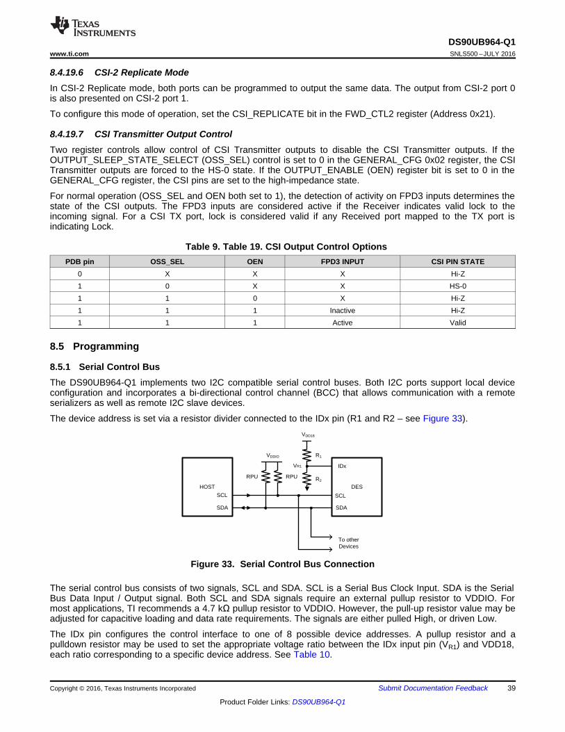
HOST DES
SCL
SDA
RPU RPU R2
SCL
SDA
To other Devices
IDx
VDD18
R1VDDIO
VR1
39
DS90UB964-Q1www.ti.com SNLS500 –JULY 2016
Product Folder Links: DS90UB964-Q1
Submit Documentation FeedbackCopyright © 2016, Texas Instruments Incorporated
8.4.19.6 CSI-2 Replicate ModeIn CSI-2 Replicate mode, both ports can be programmed to output the same data. The output from CSI-2 port 0is also presented on CSI-2 port 1.
To configure this mode of operation, set the CSI_REPLICATE bit in the FWD_CTL2 register (Address 0x21).
8.4.19.7 CSI Transmitter Output ControlTwo register controls allow control of CSI Transmitter outputs to disable the CSI Transmitter outputs. If theOUTPUT_SLEEP_STATE_SELECT (OSS_SEL) control is set to 0 in the GENERAL_CFG 0x02 register, the CSITransmitter outputs are forced to the HS-0 state. If the OUTPUT_ENABLE (OEN) register bit is set to 0 in theGENERAL_CFG register, the CSI pins are set to the high-impedance state.
For normal operation (OSS_SEL and OEN both set to 1), the detection of activity on FPD3 inputs determines thestate of the CSI outputs. The FPD3 inputs are considered active if the Receiver indicates valid lock to theincoming signal. For a CSI TX port, lock is considered valid if any Received port mapped to the TX port isindicating Lock.
Table 9. Table 19. CSI Output Control OptionsPDB pin OSS_SEL OEN FPD3 INPUT CSI PIN STATE
0 X X X Hi-Z1 0 X X HS-01 1 0 X Hi-Z1 1 1 Inactive Hi-Z1 1 1 Active Valid
8.5 Programming
8.5.1 Serial Control BusThe DS90UB964-Q1 implements two I2C compatible serial control buses. Both I2C ports support local deviceconfiguration and incorporates a bi-directional control channel (BCC) that allows communication with a remoteserializers as well as remote I2C slave devices.
The device address is set via a resistor divider connected to the IDx pin (R1 and R2 – see Figure 33).
Figure 33. Serial Control Bus Connection
The serial control bus consists of two signals, SCL and SDA. SCL is a Serial Bus Clock Input. SDA is the SerialBus Data Input / Output signal. Both SCL and SDA signals require an external pullup resistor to VDDIO. Formost applications, TI recommends a 4.7 kΩ pullup resistor to VDDIO. However, the pull-up resistor value may beadjusted for capacitive loading and data rate requirements. The signals are either pulled High, or driven Low.
The IDx pin configures the control interface to one of 8 possible device addresses. A pullup resistor and apulldown resistor may be used to set the appropriate voltage ratio between the IDx input pin (VR1) and VDD18,each ratio corresponding to a specific device address. See Table 10.

Bus Activity:Master
SDA Line
Bus Activity: Slave
Sta
rt
Slave Address
ACK
S
Address
ACK
S
Sta
rt
Slave Address
ACK
NACK
P
Sto
p
Data
0 1
Register
7-bit Address 7-bit Address
SDA
SCL
S PSTART condition, orSTART repeat condition
STOP condition
40
DS90UB964-Q1SNLS500 –JULY 2016 www.ti.com
Product Folder Links: DS90UB964-Q1
Submit Documentation Feedback Copyright © 2016, Texas Instruments Incorporated
Programming (continued)Table 10. Serial Control Bus Addresses for IDx
NO.TARGET VOLTAGE SUGGESTED R1
kΩ (1% tol)SUGGESTED R2
kΩ (1% tol)7-BIT
ADDRESS8-BIT
ADDRESSVR1 min (V) VR1 typ (V) VR1 max (V)0 0 0 0.237 OPEN 40.2 0x30 0x601 0.293 0.367 0.440 118 30.9 0x32 0x642 0.507 0.579 0.650 107 51.1 0x34 0x683 0.716 0.783 0.849 113 88.7 0x36 0x6C4 0.924 0.992 1.059 82.5 102 0x38 0x705 1.139 1.205 1.271 68.1 137 0x3A 0x746 1.350 1.416 1.481 56.2 210 0x3C 0x787 1.561 VDD18 VDD18 13.3 OPEN 0x3D 0x7A
The Serial Bus protocol is controlled by START, START-Repeated, and STOP phases. A START occurs whenSCL transitions Low while SDA is High. A STOP occurs when SDA transitions High while SCL is also HIGH. SeeFigure 34 .
Figure 34. START and STOP Conditions
To communicate with a remote device, the host controller (master) sends the slave address and listens for aresponse from the slave. This response is referred to as an acknowledge bit (ACK). If a slave on the bus isaddressed correctly, it acknowledges (ACKs) the master by driving the SDA bus low. If the address does notmatch a device's slave address, it not-acknowledges (NACKs) the master by letting SDA be pulled High. ACKsalso occur on the bus when data is being transmitted. When the master is writing data, the slave ACKs afterevery data byte is successfully received. When the master is reading data, the master ACKs after every databyte is received to let the slave know it wants to receive another data byte. When the master wants to stopreading, it NACKs after the last data byte and creates a stop condition on the bus. All communication on the busbegins with either a Start condition or a Repeated Start condition. All communication on the bus ends with a Stopcondition. A READ is shown in Figure 35 and a WRITE is shown in Figure 36.
Figure 35. Serial Control Bus — READ

SCL
SDA
START STOP
1 2 6 7 8 9 1 2 8 9
MSB
7-bit Slave Address
R/W Direction
BitAcknowledge
from the Device
MSB
Data Byte
*Acknowledgeor Not-ACK
ACK N/ACK
Repeated for the Lower Data Byte and Additional Data Transfers
LSB LSB
ACK
ACK
ACK
S P
Sto
p
Bus Activity: Slave
SDA Line
Bus Activity:Master
Slave Address Address Data
Sta
rt
0
Register
7-bit Address
41
DS90UB964-Q1www.ti.com SNLS500 –JULY 2016
Product Folder Links: DS90UB964-Q1
Submit Documentation FeedbackCopyright © 2016, Texas Instruments Incorporated
Figure 36. Serial Control Bus — WRITE
Figure 37. Basic Operation
The I2C Master located at the Deserializer must support I2C clock stretching. For more information on I2Cinterface requirements and throughput considerations, refer to I2C Communication Over FPD-Link III withBidirectional Control Channel and I2C over DS90UB913/4 FPD-Link III with Bidirectional Control Channel.
8.5.2 Second I2C PortThe DS90UB964-Q1 includes a second I2C port that allows bi-directional control channel access to both localregisters and remote devices. Remote device access is configured on BCCx_MAP register 0x0C[7:4].
The second I2C port uses the same I2C address as the primary I2C port. In addition, RX Port I2C IDs are alsoavailable for the second I2C port.
In general, TI recommends that the second I2C port be used in cases where the CSI TX ports are connected toseparate processors. The second I2C port allows independent control of the DS90UB964-Q1 as well as remotedevices by the second processor.
8.5.3 Broadcast Write to Remote DevicesThe DS90UB964-Q1 provides a mechanism to broadcast I2C writes to remote devices (either remote slaves orserializers). For each Receive port, the SlaveID/Alias register pairs would be programmed with the sameSlaveAlias value so they would each respond to the local I2C access. The SlaveID value would match theintended remote device address, either remote slave or serializers. For each receive port, on of the SlaveAliasregisters is set with an Alias value. For each port, the SlaveID value is set to the address of the remote device.These values may be the same. To access the remote serializer registers rather than a remote slave, theserializer ID (SER_IDx or SER_IDy) would be used as the SlaveID value.
8.5.3.1 Code Example for Broadcast Write# "FPD3_PORT_SEL Boardcast RX0/1/2/3"WriteI2C(0x4c,0x0f) # RX_PORT0 read; RX0/1/2/3 write
# "enable pass throu"WriteI2C(0x58,0x58) # enable pass throu
WriteI2C(0x5c,0x18) # "SER_ALIAS_ID"
WriteI2C(0x5d,0x60) # "SlaveID[0]"
WriteI2C(0x65,0x60) # "SlaveAlias[0]"

42
DS90UB964-Q1SNLS500 –JULY 2016 www.ti.com
Product Folder Links: DS90UB964-Q1
Submit Documentation Feedback Copyright © 2016, Texas Instruments Incorporated
WriteI2C(0x7c,0x01) # "FV_POLARITY"
WriteI2C(0x70,0x1f) # RAW10_datatype_yuv422b10_VC0
8.5.4 Interrupt SupportInterrupts can be brought out on the INTB pin as controlled by the INTERRUPT_CTL 0x23 andINTERRUPT_STS 0x24 registers. The main interrupt control registers provide control and status for interruptsfrom the individual sources. Sources include each of the four FPD3 Receive ports as well as each of the twoCSI-2 Transmit ports. Clearing interrupt conditions requires reading the associated status register for the source.The setting of the individual interrupt status bits is not dependent on the related interrupt enable controls. Theinterrupt enable controls whether an interrupt is generated based on the condition, but does not prevent theinterrupt status assertion.
For an interrupt to be generated based on one of the interrupt status assertions, both the individual interruptenable and the INT_EN control must be set in the INTERRUPT_CTL 0x23 register. For example, to generate aninterrupt if IS_RX0 is set, both the IE_RX0 and INT_EN bits must be set. If IE_RX0 is set but INT_EN is not, theINT status is indicated in the INTERRUPT_STS register, and the INTB pin does not indicate the interruptcondition.
See the INTERRUPT_CTL 0x23 and INTERRUPT_STS 0x24 register for details.
8.5.4.1 Code Example to Enable Interrupts# "RX01/2/3/4 INTERRUPT_CTL enable"WriteI2C(0x23,0xBF) # RX all & INTB PIN EN
# Individual RX01/2/3/4 INTERRUPT_CTL enable# "RX0 INTERRUPT_CTL enable"WriteI2C(0x4C,0x01) # RX0WriteI2C(0x23,0x81) # RX0 & INTB PIN EN
# "RX1 INTERRUPT_CTL enable"WriteI2C(0x4C,0x12) # RX1WriteI2C(0x23,0x82) # RX1 & INTB PIN EN
# "RX2 INTERRUPT_CTL enable"WriteI2C(0x4C,0x24) # RX2WriteI2C(0x23,0x84) # RX2 & INTB PIN EN
# "RX3 INTERRUPT_CTL enable"WriteI2C(0x4C,0x38) # RX3WriteI2C(0x23,0x88) # RX3 & INTB PIN EN
8.5.4.2 FPD-Link III Receive Port InterruptsFor each FPD-Link III Receive port, multiple options are available for generating interrupts. Interrupt generation iscontrolled via the PORT_ICR_HI 0xD8 and PORT_ICR_LO 0xD9 registers. In addition, the PORT_ISR_HI 0xDAand PORT_ISR_LO 0xDB registers provide read-only status for the interrupts. Clearing of interrupt conditions ishandled by reading the RX_PORT_STS1, RX_PORT_STS2, and CSI_RX_STS registers. The status bits in thePORT_ISR_HI/LO registers are copies of the associated bits in the main status registers.
To enable interrupts from one of the Receive port interrupt sources:1. Enable the interrupt source by setting the appropriate interrupt enable bit in the PORT_ICR_HI or
PORT_ICR_LO register2. Set the RX Port X Interrupt control bit (IE_RXx) in the INTERRUPT_CTL register3. Set the INT_EN bit in the INTERRUPT_CTL register to allow the interrupt to assert the INTB pin low
To clear interrupts from one of the Receive port interrupt sources:1. (optional) Read the INTERRUPT_STS register to determine which RX Port caused the interrupt2. (optional) Read the PORT_ISR_HI and PORT_ISR_LO registers to determine source of interrupt3. Read the appropriate RX_PORT_STS1, RX_PORT_STS2, or CSI_RX_STS register to clear the interrupt.

43
DS90UB964-Q1www.ti.com SNLS500 –JULY 2016
Product Folder Links: DS90UB964-Q1
Submit Documentation FeedbackCopyright © 2016, Texas Instruments Incorporated
The first two steps are optional. The interrupt could be determined and cleared by just reading the statusregisters.
8.5.4.3 Code Example to Readback InterruptsINTERRUPT_STS = ReadI2C(0x24) # 0x24 INTERRUPT_STS
if ((INTERRUPT_STS & 0x80) >> 7):print "# GLOBAL INTERRUPT DETECTED "
if ((INTERRUPT_STS & 0x40) >> 6):print "# RESERVED "
if ((INTERRUPT_STS & 0x20) >> 5):print "# IS_CSI_TX1 DETECTED "
if ((INTERRUPT_STS & 0x10) >> 4):print "# IS_CSI_TX0 DETECTED "
if ((INTERRUPT_STS & 0x08) >> 3):print "# IS_RX3 DETECTED "
if ((INTERRUPT_STS & 0x04) >> 2):print "# IS_RX2 DETECTED "
if ((INTERRUPT_STS & 0x02) >> 1):print "# IS_RX1 DETECTED "
if ((INTERRUPT_STS & 0x01) ):print "# IS_RX0 DETECTED "
# "################################################"# "RX0 status"# "################################################"
WriteReg(0x4C,0x01) # RX0PORT_ISR_LO = ReadI2C(0xDB)
print "0xDB PORT_ISR_LO : ", hex(PORT_ISR_LO) # readout; cleared by RX_PORT_STS2
if ((PORT_ISR_LO & 0x40) >> 6):print "# IS_LINE_LEN_CHG INTERRUPT DETECTED "
if ((PORT_ISR_LO & 0x20) >> 5):print "# IS_LINE_CNT_CHG DETECTED "
if ((PORT_ISR_LO & 0x10) >> 4):print "# IS_BUFFER_ERR DETECTED "
if ((PORT_ISR_LO & 0x08) >> 3):print "# IS_CSI_RX_ERR DETECTED "
if ((PORT_ISR_LO & 0x04) >> 2):print "# IS_FPD3_PAR_ERR DETECTED "
if ((PORT_ISR_LO & 0x02) >> 1):print "# IS_PORT_PASS DETECTED "
if ((PORT_ISR_LO & 0x01) ) :print "# IS_LOCK_STS DETECTED "
################################################
PORT_ISR_HI = ReadI2C(0xDA)
print "0xDA PORT_ISR_HI : ", hex(PORT_ISR_HI) # readout; cleared by RX_PORT_STS2
if ((PORT_ISR_HI & 0x04) >> 2):print "# IS_FPD3_ENC_ERR DETECTED "
if ((PORT_ISR_HI & 0x02) >> 1):print "# IS_BCC_SEQ_ERR DETECTED "
if ((PORT_ISR_HI & 0x01) ) :print "# IS_BCC_CRC_ERR DETECTED "
################################################
RX_PORT_STS1 = ReadI2C(0x4D) # R/COR
if ( (RX_PORT_STS1 & 0xc0) >> 6) == 3:print "# RX_PORT_NUM = RX3"
elif ((RX_PORT_STS1 & 0xc0) >> 6) == 2:print "# RX_PORT_NUM = RX2"
elif ((RX_PORT_STS1 & 0xc0) >> 6) == 1:print "# RX_PORT_NUM = RX1"
elif ((RX_PORT_STS1 & 0xc0) >> 6) == 0:

44
DS90UB964-Q1SNLS500 –JULY 2016 www.ti.com
Product Folder Links: DS90UB964-Q1
Submit Documentation Feedback Copyright © 2016, Texas Instruments Incorporated
print "# RX_PORT_NUM = RX0"
if ((RX_PORT_STS1 & 0x20) >> 5):print "# BCC_CRC_ERR DETECTED "
if ((RX_PORT_STS1 & 0x10) >> 4):print "# LOCK_STS_CHG DETECTED "
if ((RX_PORT_STS1 & 0x08) >> 3):print "# BCC_SEQ_ERROR DETECTED "
if ((RX_PORT_STS1 & 0x04) >> 2):print "# PARITY_ERROR DETECTED "
if ((RX_PORT_STS1 & 0x02) >> 1):print "# PORT_PASS=1 "
if ((RX_PORT_STS1 & 0x01) ):print "# LOCK_STS=1 "
################################################
RX_PORT_STS2 = ReadI2C(0x4E)
if ((RX_PORT_STS2 & 0x80) >> 7):print "# LINE_LEN_UNSTABLE DETECTED "
if ((RX_PORT_STS2 & 0x40) >> 6):print "# LINE_LEN_CHG "
if ((RX_PORT_STS2 & 0x20) >> 5):print "# FPD3_ENCODE_ERROR DETECTED "
if ((RX_PORT_STS2 & 0x10) >> 4):print "# BUFFER_ERROR DETECTED "
if ((RX_PORT_STS2 & 0x08) >> 3):print "# CSI_ERR DETECTED "
if ((RX_PORT_STS2 & 0x04) >> 2):print "# FREQ_STABLE DETECTED "
if ((RX_PORT_STS2 & 0x02) >> 1):print "# NO_FPD3_CLK DETECTED "
if ((RX_PORT_STS2 & 0x01) ):print "# LINE_CNT_CHG DETECTED "
################################################
# "################################################"# "RX1 status"# "################################################"
WriteReg(0x4C,0x12) # RX1PORT_ISR_LO = ReadI2C(0xDB) # PORT_ISR_LO readout; cleared by RX_PORT_STS2
if ((PORT_ISR_LO & 0x40) >> 6):print "# IS_LINE_LEN_CHG INTERRUPT DETECTED "
if ((PORT_ISR_LO & 0x20) >> 5):print "# IS_LINE_CNT_CHG DETECTED "
if ((PORT_ISR_LO & 0x10) >> 4):print "# IS_BUFFER_ERR DETECTED "
if ((PORT_ISR_LO & 0x08) >> 3):print "# IS_CSI_RX_ERR DETECTED "
if ((PORT_ISR_LO & 0x04) >> 2):print "# IS_FPD3_PAR_ERR DETECTED "
if ((PORT_ISR_LO & 0x02) >> 1):print "# IS_PORT_PASS DETECTED "
if ((PORT_ISR_LO & 0x01) ) :print "# IS_LOCK_STS DETECTED "
################################################
PORT_ISR_HI = ReadI2C(0xDA) # readout; cleared by RX_PORT_STS2
if ((PORT_ISR_HI & 0x04) >> 2):print "# IS_FPD3_ENC_ERR DETECTED "
if ((PORT_ISR_HI & 0x02) >> 1):print "# IS_BCC_SEQ_ERR DETECTED "
if ((PORT_ISR_HI & 0x01) ) :print "# IS_BCC_CRC_ERR DETECTED "
################################################

45
DS90UB964-Q1www.ti.com SNLS500 –JULY 2016
Product Folder Links: DS90UB964-Q1
Submit Documentation FeedbackCopyright © 2016, Texas Instruments Incorporated
RX_PORT_STS1 = ReadI2C(0x4D) # R/COR
if ( (RX_PORT_STS1 & 0xc0) >> 6) == 3:print "# RX_PORT_NUM = RX3"
elif ((RX_PORT_STS1 & 0xc0) >> 6) == 2:print "# RX_PORT_NUM = RX2"
elif ((RX_PORT_STS1 & 0xc0) >> 6) == 1:print "# RX_PORT_NUM = RX1"
elif ((RX_PORT_STS1 & 0xc0) >> 6) == 0:print "# RX_PORT_NUM = RX0"
if ((RX_PORT_STS1 & 0x20) >> 5):print "# BCC_CRC_ERR DETECTED "
if ((RX_PORT_STS1 & 0x10) >> 4):print "# LOCK_STS_CHG DETECTED "
if ((RX_PORT_STS1 & 0x08) >> 3):print "# BCC_SEQ_ERROR DETECTED "
if ((RX_PORT_STS1 & 0x04) >> 2):print "# PARITY_ERROR DETECTED "
if ((RX_PORT_STS1 & 0x02) >> 1):print "# PORT_PASS=1 "
if ((RX_PORT_STS1 & 0x01) ):print "# LOCK_STS=1 "
################################################
RX_PORT_STS2 = ReadI2C(0x4E)
if ((RX_PORT_STS2 & 0x80) >> 7):print "# LINE_LEN_UNSTABLE DETECTED "
if ((RX_PORT_STS2 & 0x40) >> 6):print "# LINE_LEN_CHG "
if ((RX_PORT_STS2 & 0x20) >> 5):print "# FPD3_ENCODE_ERROR DETECTED "
if ((RX_PORT_STS2 & 0x10) >> 4):print "# BUFFER_ERROR DETECTED "
if ((RX_PORT_STS2 & 0x08) >> 3):print "# CSI_ERR DETECTED "
if ((RX_PORT_STS2 & 0x04) >> 2):print "# FREQ_STABLE DETECTED "
if ((RX_PORT_STS2 & 0x02) >> 1):print "# NO_FPD3_CLK DETECTED "
if ((RX_PORT_STS2 & 0x01) ):print "# LINE_CNT_CHG DETECTED "
################################################
# "################################################"# "RX2 status"# "################################################"
WriteReg(0x4C,0x24) # RX2PORT_ISR_LO = ReadI2C(0xDB) # readout; cleared by RX_PORT_STS2
if ((PORT_ISR_LO & 0x40) >> 6):print "# IS_LINE_LEN_CHG INTERRUPT DETECTED "
if ((PORT_ISR_LO & 0x20) >> 5):print "# IS_LINE_CNT_CHG DETECTED "
if ((PORT_ISR_LO & 0x10) >> 4):print "# IS_BUFFER_ERR DETECTED "
if ((PORT_ISR_LO & 0x08) >> 3):print "# IS_CSI_RX_ERR DETECTED "
if ((PORT_ISR_LO & 0x04) >> 2):print "# IS_FPD3_PAR_ERR DETECTED "
if ((PORT_ISR_LO & 0x02) >> 1):print "# IS_PORT_PASS DETECTED "
if ((PORT_ISR_LO & 0x01) ) :print "# IS_LOCK_STS DETECTED "
################################################
PORT_ISR_HI = ReadI2C(0xDA) # readout; cleared by RX_PORT_STS2

46
DS90UB964-Q1SNLS500 –JULY 2016 www.ti.com
Product Folder Links: DS90UB964-Q1
Submit Documentation Feedback Copyright © 2016, Texas Instruments Incorporated
if ((PORT_ISR_HI & 0x04) >> 2):print "# IS_FPD3_ENC_ERR DETECTED "
if ((PORT_ISR_HI & 0x02) >> 1):print "# IS_BCC_SEQ_ERR DETECTED "
if ((PORT_ISR_HI & 0x01) ) :print "# IS_BCC_CRC_ERR DETECTED "
################################################
RX_PORT_STS1 = ReadI2C(0x4D) # R/COR
if ( (RX_PORT_STS1 & 0xc0) >> 6) == 3:print "# RX_PORT_NUM = RX3"
elif ((RX_PORT_STS1 & 0xc0) >> 6) == 2:print "# RX_PORT_NUM = RX2"
elif ((RX_PORT_STS1 & 0xc0) >> 6) == 1:print "# RX_PORT_NUM = RX1"
elif ((RX_PORT_STS1 & 0xc0) >> 6) == 0:print "# RX_PORT_NUM = RX0"
if ((RX_PORT_STS1 & 0x20) >> 5):print "# BCC_CRC_ERR DETECTED "
if ((RX_PORT_STS1 & 0x10) >> 4):print "# LOCK_STS_CHG DETECTED "
if ((RX_PORT_STS1 & 0x08) >> 3):print "# BCC_SEQ_ERROR DETECTED "
if ((RX_PORT_STS1 & 0x04) >> 2):print "# PARITY_ERROR DETECTED "
if ((RX_PORT_STS1 & 0x02) >> 1):print "# PORT_PASS=1 "
if ((RX_PORT_STS1 & 0x01) ):print "# LOCK_STS=1 "
################################################
RX_PORT_STS2 = ReadI2C(0x4E)
if ((RX_PORT_STS2 & 0x80) >> 7):print "# LINE_LEN_UNSTABLE DETECTED "
if ((RX_PORT_STS2 & 0x40) >> 6):print "# LINE_LEN_CHG "
if ((RX_PORT_STS2 & 0x20) >> 5):print "# FPD3_ENCODE_ERROR DETECTED "
if ((RX_PORT_STS2 & 0x10) >> 4):print "# BUFFER_ERROR DETECTED "
if ((RX_PORT_STS2 & 0x08) >> 3):print "# CSI_ERR DETECTED "
if ((RX_PORT_STS2 & 0x04) >> 2):print "# FREQ_STABLE DETECTED "
if ((RX_PORT_STS2 & 0x02) >> 1):print "# NO_FPD3_CLK DETECTED "
if ((RX_PORT_STS2 & 0x01) ):print "# LINE_CNT_CHG DETECTED "
################################################
# "################################################"# "RX3 status"# "################################################"
WriteReg(0x4C,0x38) # RX3PORT_ISR_LO = ReadI2C(0xDB) # readout; cleared by RX_PORT_STS2
if ((PORT_ISR_LO & 0x40) >> 6):print "# IS_LINE_LEN_CHG INTERRUPT DETECTED "
if ((PORT_ISR_LO & 0x20) >> 5):print "# IS_LINE_CNT_CHG DETECTED "
if ((PORT_ISR_LO & 0x10) >> 4):print "# IS_BUFFER_ERR DETECTED "
if ((PORT_ISR_LO & 0x08) >> 3):print "# IS_CSI_RX_ERR DETECTED "

47
DS90UB964-Q1www.ti.com SNLS500 –JULY 2016
Product Folder Links: DS90UB964-Q1
Submit Documentation FeedbackCopyright © 2016, Texas Instruments Incorporated
if ((PORT_ISR_LO & 0x04) >> 2):print "# IS_FPD3_PAR_ERR DETECTED "
if ((PORT_ISR_LO & 0x02) >> 1):print "# IS_PORT_PASS DETECTED "
if ((PORT_ISR_LO & 0x01) ) :print "# IS_LOCK_STS DETECTED "
################################################
PORT_ISR_HI = ReadI2C(0xDA) # readout; cleared by RX_PORT_STS2
if ((PORT_ISR_HI & 0x04) >> 2):print "# IS_FPD3_ENC_ERR DETECTED "
if ((PORT_ISR_HI & 0x02) >> 1):print "# IS_BCC_SEQ_ERR DETECTED "
if ((PORT_ISR_HI & 0x01) ) :print "# IS_BCC_CRC_ERR DETECTED "
################################################
RX_PORT_STS1 = ReadI2C(0x4D) # R/COR
if ( (RX_PORT_STS1 & 0xc0) >> 6) == 3:print "# RX_PORT_NUM = RX3"
elif ((RX_PORT_STS1 & 0xc0) >> 6) == 2:print "# RX_PORT_NUM = RX2"
elif ((RX_PORT_STS1 & 0xc0) >> 6) == 1:print "# RX_PORT_NUM = RX1"
elif ((RX_PORT_STS1 & 0xc0) >> 6) == 0:print "# RX_PORT_NUM = RX0"
if ((RX_PORT_STS1 & 0x20) >> 5):print "# BCC_CRC_ERR DETECTED "
if ((RX_PORT_STS1 & 0x10) >> 4):print "# LOCK_STS_CHG DETECTED "
if ((RX_PORT_STS1 & 0x08) >> 3):print "# BCC_SEQ_ERROR DETECTED "
if ((RX_PORT_STS1 & 0x04) >> 2):print "# PARITY_ERROR DETECTED "
if ((RX_PORT_STS1 & 0x02) >> 1):print "# PORT_PASS=1 "
if ((RX_PORT_STS1 & 0x01) ):print "# LOCK_STS=1 "
################################################
RX_PORT_STS2 = ReadI2C(0x4E)
if ((RX_PORT_STS2 & 0x80) >> 7):print "# LINE_LEN_UNSTABLE DETECTED "
if ((RX_PORT_STS2 & 0x40) >> 6):print "# LINE_LEN_CHG "
if ((RX_PORT_STS2 & 0x20) >> 5):print "# FPD3_ENCODE_ERROR DETECTED "
if ((RX_PORT_STS2 & 0x10) >> 4):print "# BUFFER_ERROR DETECTED "
if ((RX_PORT_STS2 & 0x08) >> 3):print "# CSI_ERR DETECTED "
if ((RX_PORT_STS2 & 0x04) >> 2):print "# FREQ_STABLE DETECTED "
if ((RX_PORT_STS2 & 0x02) >> 1):print "# NO_FPD3_CLK DETECTED "
if ((RX_PORT_STS2 & 0x01) ):print "# LINE_CNT_CHG DETECTED "
################################################
8.5.4.4 CSI-2 Transmit Port InterruptsThe following interrupts are available for each CSI Transmit Port:• Pass indication• Synchronized status

48
DS90UB964-Q1SNLS500 –JULY 2016 www.ti.com
Product Folder Links: DS90UB964-Q1
Submit Documentation Feedback Copyright © 2016, Texas Instruments Incorporated
• Deassertion of Pass indication for an input port assigned to the CSI TX Port• Loss of Synchronization between input video streams• RX Port Interrupt – interrupts from RX Ports mapped to this CSI Transmit port
See the CSI_TX_ICR address 0x36 and CSI_TX_ISR address 0x37 registers for details.
The setting of the individual interrupt status bits is not dependent on the related interrupt enable controls. Theinterrupt enable controls whether an interrupt is generated based on the condition, but does not prevent theinterrupt status assertion.
8.5.5 Timestamp – Video Skew DetectionThe DS90UB964-Q1 implements logic to detect skew between video signaling from attached cameras. For eachinput port, the DS90UB964-Q1 provides the ability to capture a time-stamp for both a start-of-frame and start-of-line event. Comparison of timestamps can provide information on the relative skew between the ports. Start-of-frame timestamps are generated at the active edge of the Vertical Sync signal in Raw mode. Start-of-linetimestamps are generated at the start of reception of the Nth line of video data after the start-of-frame for eithermode of operation. The function does not use the Line Start (LS) packet or Horizontal Sync controls to determinethe start of lines.
The skew detection can run in either a FrameSync mode or free-run mode.
Skew detection can be individually enabled for each RX port.
For start-of-line timestamps, a line number must be programmed. The same line number is used for all 4channels. Prior to reading timestamps, the TS_FREEZE bit for each port that will be read should be set. This willprevent overwrite of the timestamps by the detection circuit until all timestamps have been read. The freezecondition will be released automatically once all frozen timestamps have been read. The freeze bits can also becleared if it does not read all the timestamp values.
The TS_STATUS register includes the following:• Flags to indicate multiple start-of-frame per FrameSync period• Flag to indicate Timestamps Ready• Flags to indicate Timestamps valid (per port) – if ports are not synchronized, all ports may not indicate valid
timestamps
The Timestamp Ready flag will be cleared when the TS_FREEZE bit is cleared.
8.5.6 Pattern GenerationThe DS90UB964-Q1 supports an internal pattern generation feature to provide a simple way to generate videotest patterns for the CSI-2 transmitter outputs. Two types of patterns are supported: Reference Color Bar patternand Fixed Color patterns.
The Pattern Generator is programmable with the following options:• Number of color bars (1, 2, 4, or 8)• Number of bytes per line• Number of bytes per color bar• CSI DataType field and VC-ID• Number of active video lines per frame• Number of total lines per frame (active plus blanking)• Line period• Vertical front porch – number of blank lines prior to FrameEnd packet• Vertical back porch – number of blank lines following FrameStart packet
8.5.6.1 Code Example for Pattern Generator#Patgen Fixed Colorbar 1280x720p30
WriteI2C(0x32,0x01) # CSI0 sel and CSI0 enableWriteI2C(0x33,0x01)
WriteI2C(0xB0,0x00) # Indirect Pattern Gen Registers

49
DS90UB964-Q1www.ti.com SNLS500 –JULY 2016
Product Folder Links: DS90UB964-Q1
Submit Documentation FeedbackCopyright © 2016, Texas Instruments Incorporated
WriteI2C(0xB1,0x01) # PGEN_CTLWriteI2C(0xB2,0x01)
WriteI2C(0xB1,0x02) # PGEN_CFGWriteI2C(0xB2,0x33)
WriteI2C(0xB1,0x03) # PGEN_CSI_DIWriteI2C(0xB2,0x24)
WriteI2C(0xB1,0x04) # PGEN_LINE_SIZE1WriteI2C(0xB2,0x0F)
WriteI2C(0xB1,0x05) # PGEN_LINE_SIZE0WriteI2C(0xB2,0x00)
WriteI2C(0xB1,0x06) # PGEN_BAR_SIZE1WriteI2C(0xB2,0x01)
WriteI2C(0xB1,0x07) # PGEN_BAR_SIZE0WriteI2C(0xB2,0xE0)
WriteI2C(0xB1,0x08) # PGEN_ACT_LPF1WriteI2C(0xB2,0x02)
WriteI2C(0xB1,0x09) # PGEN_ACT_LPF0WriteI2C(0xB2,0xD0)
WriteI2C(0xB1,0x0A) # PGEN_TOT_LPF1WriteI2C(0xB2,0x04)
WriteI2C(0xB1,0x0B) # PGEN_TOT_LPF0WriteI2C(0xB2,0x1A)
WriteI2C(0xB1,0x0C) # PGEN_LINE_PD1WriteI2C(0xB2,0x0C)
WriteI2C(0xB1,0x0D) # PGEN_LINE_PD0WriteI2C(0xB2,0x67)
WriteI2C(0xB1,0x0E) # PGEN_VBPWriteI2C(0xB2,0x21)
WriteI2C(0xB1,0x0F) # PGEN_VFPWriteI2C(0xB2,0x0A)
8.5.7 BISTAn optional At-Speed Built-In Self Test (BIST) feature supports testing of the high speed serial link and the backchannel without external data connections. This is useful in the prototype stage, equipment production, in-systemtest, and system diagnostics.
8.5.7.1 BIST Configuration and StatusThe BIST mode is enabled by BIST configuration register 0xB3. The test may select either an external PCLK orthe internal oscillator clock (OSC) frequency in the Serializer. In the absence of PCLK, the user can select theinternal OSC frequency at the deserializer through the BIST configuration register. When BIST is activated at thedeserializer, a BIST enable signal is sent to the serializer through the Back Channel. The serializer outputs acontinuous stream of a pseudo-random sequence and drives the link at speed. The deserializer detects the testpattern and monitors it for errors. The serializer also tracks errors indicated by the CRC fields in each backchannel frame. While the lock indications are required to identify the beginning of proper data reception, for anylink failures or data corruption, the best indication is the contents of the error counter in the BIST_ERR_COUNTregister 0x57 for each RX port.

50
DS90UB964-Q1SNLS500 –JULY 2016 www.ti.com
Product Folder Links: DS90UB964-Q1
Submit Documentation Feedback Copyright © 2016, Texas Instruments Incorporated
8.6 Register DescriptionThe DS90UB964-Q1 implements the following register blocks, accessible via I2C as well as the bi-directionalcontrol channel:• Main Registers• FPD3 RX Port Registers (separate register block for each of the four RX ports)• CSI-2 Port Registers (separate register block for each of the CSI-2 ports)
Table 11. Main Register Map DescriptionsADDRESSRANGE DESCRIPTION ADDRESS MAP0x00-0x31 Digital Shared Registers Shared0x32-0x3A Digital CSI-2 Registers
(paged, broadcast write allowed)CSI-2 TX Port 0R: 0x32[4]=0W: 0x32[0]=1
CSI-2 TX Port 1R: 0x32[4]=1W: 0x32[1]=1
0x4C-0x7F Digital RX Port Registers(paged, broadcast write allowed)
FPD3 RX Port 0R: 0x4C[5:4]=00W: 0x4C[0]=1
FPD3 RX Port 1R: 0x4C[5:4]=01W: 0x4C[1]=1
FPD3 RX Port 2R: 0x4C[5:4]=10W: 0x4C[2]=1
FPD3 RX Port 3R: 0x4C[5:4]=11W: 0x4C[3]=1
0x80-0x9F Reserved Reserved0xA0-0xAF Reserved Reserved0xB0-0xB2 Indirect Access Registers Shared0xB0-0xBF Digital Share Registers Shared0xC0-0xCF Reserved Reserved0xD0-0xDF Digital RX Port Debug Registers FPD3 RX Port 0 FPD3 RX Port 1 FPD3 RX Port 2 FPD3 RX Port 30xE0-0xEF Reserved Reserved0xF0-0xF5 FPD3 RX ID Shared0xF8-0xFB Port I2C Addressing Shared0xF6-0xF70xFC-0xFF
Reserved Reserved
LEGEND:• RW = Read Write• RW/SC = RW/SC = Read Write access/Self Clearing bit• R = Read Only, Permanent value• R/COR = Read Only, Clear On Read

51
DS90UB964-Q1www.ti.com SNLS500 –JULY 2016
Product Folder Links: DS90UB964-Q1
Submit Documentation FeedbackCopyright © 2016, Texas Instruments Incorporated
8.7 Register Maps
Table 12. Serial Control Bus RegistersPage Addr
(hex)Register Name Bit(s) Field Type Default Description
Share 0x00 I2C_DEVICE_ID 7:1 DEVICE_ID RW Strap 7-bit I2C ID of Deserializer.This field always indicates the current value ofthe I2C ID. When bit 0 of this register is 0, thisfield is read-only and show the strapped ID.When bit 0 of this register is 1, this field isread/write and can be used to assign any validI2C ID.
0 DES_ID RW 0 0: Device ID is from strap1: Register I2C Device ID overrides strappedvalue
Share 0x01 RESET_CTL 7:6 RESERVED R 0x0 Reserved5 RESERVED RW 0 Reserved4:3 RESERVED R 0x0 Reserved2 RESTART_AUTOLO
ADRW/SC 0 Restart ROM Auto-load
Setting this bit to 1 causes a re-load of theROM. This bit is self-clearing. Software maycheck for Auto-load complete by checking theCFG_INIT_DONE bit in the DEVICE_STSregister.
1 DIGITAL RESET1 RW/SC 0 Digital ResetResets the entire digital block includingregisters. This bit is self-clearing.1: Reset0: Normal operation
0 DIGITAL RESET0 RW/SC 0 Digital ResetResets the entire digital block except registers.This bit is self-clearing.1: Reset0: Normal operation
Share 0x02 GENERAL_CFG 7:5 RESERVED R 0x0 Reserved4 OUTPUT_EN_MODE RW 1 Output Enable Mode
If set to 0, the CSI TX output port is forced tothe high-impedance state if no assigned RXports have an active Receiver lock.If set to 1, the CSI TX output port will continuein normal operation if no assigned RX portshave an active Receiver lock. CSI TXoperation will remain under register control viathe CSI_CTL register for each port. If noassigned RX ports have an active Receiverlock, this will result in the CSI Transmitterentering the LP-11 state.
3 OUTPUT_ENABLE RW 1 Output Enable Control (in conjunction withOutput Sleep State Select)If OUTPUT_SLEEP_STATE_SEL is set to 1and this bit is set to 0, the CSI TX outputs isforced into a high impedance state.
2 OUTPUT_SLEEP_STATE_SEL
RW 1 OSS Select to control output state when LOCKis low (used in conjunction with Output Enable)When this bit is set to 0, the CSI TX outputs isforced into a HS-0 state.
1 RX_PARITY_CHECKER_EN
RW 1 FPD3 Receiver Parity Checker Enable Whenenabled, the parity check function is enabledfor the FPD3 receiver. This allows detection oferrors on the FPD3 receiver data bits.0: Disable1: Enable

52
DS90UB964-Q1SNLS500 –JULY 2016 www.ti.com
Product Folder Links: DS90UB964-Q1
Submit Documentation Feedback Copyright © 2016, Texas Instruments Incorporated
Register Maps (continued)Table 12. Serial Control Bus Registers (continued)
Page Addr(hex)
Register Name Bit(s) Field Type Default Description
0 FORCE_REFCLK_DET
RW 0 Force indication of external reference clock0: Normal operation, reference clock detectcircuit indicates the presence of an externalreference clock1: Force reference clock to be indicatedpresent
Share 0x03 REV_MASK_ID 7:4 REVISION_ID R 0x0 Revision ID0010: DS90UB964-Q1 A00011: DS90UB964-Q1 A1
3:0 MASK_ID R 0x0 Mask IDShare 0x04 DEVICE_STS 7 CFG_CKSUM_STS R 1 Config Checksum Passed
This bit is set following initialization if theConfiguration data in the eFuse ROM had avalid checksum
6 CFG_INIT_DONE R 1 Power-up initialization completeThis bit is set after Initialization is complete.Configuration from eFuse ROM has completed.
5:0 RESERVED R 0x2 ReservedShare 0x05 PAR_ERR_THOLD_
HI7:0 PAR_ERR_THOLD_
HIRW 0x1 FPD3 Parity Error Threshold High byte
This register provides the 8 most significantbits of the Parity Error Threshold value. Foreach port, if the FPD-Link III receiver detects anumber of parity errors greater than or equal tothis value, the PARITY_ERROR flag is set inthe RX_PORT_STS1 register.
Share 0x06 PAR_ERR_THOLD_LO
7:0 PAR_ERR_THOLD_LO
RW 0x0 FPD3 Parity Error Threshold Low byteThis register provides the 8 least significantbits of the Parity Error Threshold value. Foreach port, if the FPD-Link III receiver detects anumber of parity errors greater than or equal tothis value, the PARITY_ERROR flag is set inthe RX_PORT_STS1 register.
Share 0x07 BCC WatchdogControl
7:1 BCC WATCHDOGTIMER
RW 0x7F The watchdog timer allows termination of acontrol channel transaction if it fails tocomplete within a programmed amount of time.This field sets the Bi-directional ControlChannel Watchdog Timeout value in units of 2milliseconds. This field should not be set to 0.
0 BCC WATCHDOGTIMER DISABLE
RW 0 Disable Bi-directional Control ChannelWatchdog Timer1: Disables BCC Watchdog Timer operation0: Enables BCC Watchdog Timer operation
Share 0x08 I2C Control 1 7 LOCAL WRITEDISABLE
RW 0 Disable Remote Writes to Local RegistersSetting this bit to a 1 will prevent remote writesto local device registers from across the controlchannel. This prevents writes to theDeserializer registers from an I2C masterattached to the Serializer. Setting this bit doesnot affect remote access to I2C slaves at theDeserializer.
6:4 I2C SDA HOLD RW 0x1 Internal SDA Hold TimeThis field configures the amount of internalhold time provided for the SDA input relative tothe SCL input. Units are 50 nanoseconds.
3:0 I2C FILTER DEPTH RW 0xC I2C Glitch Filter DepthThis field configures the maximum width ofglitch pulses on the SCL and SDA inputs thatis rejected. Units are 5 nanoseconds.
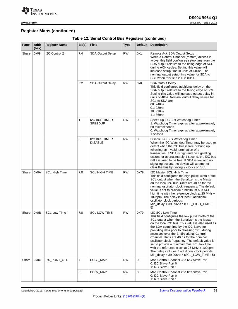
53
DS90UB964-Q1www.ti.com SNLS500 –JULY 2016
Product Folder Links: DS90UB964-Q1
Submit Documentation FeedbackCopyright © 2016, Texas Instruments Incorporated
Register Maps (continued)Table 12. Serial Control Bus Registers (continued)
Page Addr(hex)
Register Name Bit(s) Field Type Default Description
Share 0x09 I2C Control 2 7:4 SDA Output Setup RW 0x1 Remote Ack SDA Output SetupWhen a Control Channel (remote) access isactive, this field configures setup time from theSDA output relative to the rising edge of SCLduring ACK cycles. Setting this value willincrease setup time in units of 640ns. Thenominal output setup time value for SDA toSCL when this field is 0 is 80ns.
3:2 SDA Output Delay RW 0x0 SDA Output DelayThis field configures additional delay on theSDA output relative to the falling edge of SCL.Setting this value will increase output delay inunits of 40ns. Nominal output delay values forSCL to SDA are:00: 240ns01: 280ns10: 320ns11: 360ns
1 I2C BUS TIMERSPEEDUP
RW 0 Speed up I2C Bus Watchdog Timer1: Watchdog Timer expires after approximately50 microseconds0: Watchdog Timer expires after approximately1 second.
0 I2C BUS TIMERDISABLE
RW 0 Disable I2C Bus Watchdog TimerWhen the I2C Watchdog Timer may be used todetect when the I2C bus is free or hung upfollowing an invalid termination of atransaction. If SDA is high and no signallingoccurs for approximately 1 second, the I2C buswill assumed to be free. If SDA is low and nosignaling occurs, the device will attempt toclear the bus by driving 9 clocks on SCL
Share 0x0A SCL High Time 7:0 SCL HIGH TIME RW 0x79 I2C Master SCL High TimeThis field configures the high pulse width of theSCL output when the Serializer is the Masteron the local I2C bus. Units are 40 ns for thenominal oscillator clock frequency. The defaultvalue is set to provide a minimum 5us SCLhigh time with the reference clock at 25 MHz +100ppm. The delay includes 5 additionaloscillator clock periods.Min_delay = 39.996ns * (SCL_HIGH_TIME +5)
Share 0x0B SCL Low Time 7:0 SCL LOW TIME RW 0x79 I2C SCL Low TimeThis field configures the low pulse width of theSCL output when the Serializer is the Masteron the local I2C bus. This value is also used asthe SDA setup time by the I2C Slave forproviding data prior to releasing SCL duringaccesses over the Bi-directional ControlChannel. Units are 40 ns for the nominaloscillator clock frequency. The default value isset to provide a minimum 5us SCL low timewith the reference clock at 25 MHz + 100ppm.The delay includes 5 additional clock periods.Min_delay = 39.996ns * (SCL_LOW_TIME+ 5)
Share 0x0C RX_PORT_CTL 7 BCC3_MAP RW 0 Map Control Channel 3 to I2C Slave Port0: I2C Slave Port 01: I2C Slave Port 1
6 BCC2_MAP RW 0 Map Control Channel 2 to I2C Slave Port0: I2C Slave Port 01: I2C Slave Port 1

54
DS90UB964-Q1SNLS500 –JULY 2016 www.ti.com
Product Folder Links: DS90UB964-Q1
Submit Documentation Feedback Copyright © 2016, Texas Instruments Incorporated
Register Maps (continued)Table 12. Serial Control Bus Registers (continued)
Page Addr(hex)
Register Name Bit(s) Field Type Default Description
5 BCC1_MAP RW 0 Map Control Channel 1 to I2C Slave Port0: I2C Slave Port 01: I2C Slave Port 1
4 BCC0_MAP RW 0 Map Control Channel 0 to I2C Slave Port0: I2C Slave Port 01: I2C Slave Port 1
3 PORT3_EN RW 1 Port 3 Receiver Enable0: Disable Port 3 Receiver1: Enable Port 3 Receiver
2 PORT2_EN RW 1 Port 2 Receiver Enable0: Disable Port 2 Receiver1: Enable Port 2 Receiver
1 PORT1_EN RW 1 Port 1 Receiver Enable0: Disable Port 1 Receiver1: Enable Port 1 Receiver
0 PORT0_EN RW 1 Port 0 Receiver Enable0: Disable Port 0 Receiver1: Enable Port 0 Receiver
Share 0x0D IO_CTL 7 SEL3P3V RW 0 3.3V I/O Select on pins INTB, I2C, GPIO0: 1.8V I/O Supply1: 3.3V I/O SupplyIf IO_SUPPLY_MODE_OV is 0, a read of thisregister will return the detected I/O voltagelevel.
6 IO_SUPPLY_MODE_OV
RW 0 Override I/O Supply Mode bitIf set to 0, the detected voltage level is usedfor both SEL3P3V and IO_SUPPLY_MODEcontrols.If set to 1, the values written to the SEL3P3Vand IO_SUPPLY_MODE fields is used.
5:4 IO_SUPPLY_MODE RW 0x0 I/O Supply Mode00: 1.8V11: 3.3VIf IO_SUPPLY_MODE_OV is 0, a read of thisregister will return the detected I/O voltagelevel.
3:0 RESERVED RW 0x9 ReservedShare 0x0E GPIO_PIN_STS 7:0 GPIO_STS R 0x0 GPIO Pin Status
This register reads the current values on eachof the 8 GPIO pins. Bit 7 reads GPIO7 and bit0 reads GPIO0.
Share 0x0F GPIO_INPUT_CTL 7 GPIO7_INPUT_EN RW 1 GPIO7 Input Enable0: Disabled1: Enabled
6 GPIO6_INPUT_EN RW 1 GPIO6 Input Enable0: Disabled1: Enabled
5 GPIO5_INPUT_EN RW 1 GPIO5 Input Enable0: Disabled1: Enabled
4 GPIO4_INPUT_EN RW 1 GPIO4 Input Enable0: Disabled1: Enabled
3 GPIO3_INPUT_EN RW 1 GPIO3 Input Enable0: Disabled1: Enabled

55
DS90UB964-Q1www.ti.com SNLS500 –JULY 2016
Product Folder Links: DS90UB964-Q1
Submit Documentation FeedbackCopyright © 2016, Texas Instruments Incorporated
Register Maps (continued)Table 12. Serial Control Bus Registers (continued)
Page Addr(hex)
Register Name Bit(s) Field Type Default Description
2 GPIO2_INPUT_EN RW 1 GPIO2 Input Enable0: Disabled1: Enabled
1 GPIO1_INPUT_EN RW 1 GPIO1 Input Enable0: Disabled1: Enabled
0 GPIO0_INPUT_EN RW 1 GPIO0 Input Enable0: Disabled1: Enabled
Share 0x10 GPIO0_PIN_CTL 7:5 GPIO0_OUT_SEL RW 0x0 GPIO0 Output SelectDetermines the output data for the selectedsource.
If GPIO0_OUT_SRC is set to 0xx (one of theRX Ports), the following selections apply:000 : Received GPIO0001 : Received GPIO1010 : Received GPIO2011 : Received GPIO3100 : RX Port Lock indication101 : RX Port Pass indication110 : Frame Valid signal111 : Line Valid signal
If GPIO0_OUT_SRC is set to 100 (DeviceStatus), the following selections apply:000 : Value in GPIO0_OUT_VAL001 : Logical OR of Lock indication fromenabled RX ports010 : Logical AND of Lock indication fromenabled RX ports011 : Logical AND of Pass indication fromenabled RX ports100 : FrameSync signal101 - 111 : Reserved
If GPIO0_OUT_SRC is set to 11x (one of theCSI Transmit ports), the following selectionsapply:000 : Pass (AND of selected RX port status)001 : Pass (OR of selected RX port status)010 : Frame Valid (sending video frame)011 : Line Valid (sending video line)100 : Synchronized - multi-port data issynchronized101 : CSI TX Port Interrupt11 : Reserved
4:2 GPIO0_OUT_SRC RW 0x0 GPIO0 Output Source SelectSelects output source for GPIO0 data:000 : RX Port 0001 : RX Port 1010 : RX Port 2011 : RX Port 3100 : Device Status101 : Reserved110 : CSI TX Port 0111 : CSI TX Port 1
1 GPIO0_OUT_VAL RW 0 GPIO0 Output ValueThis register provides the output data valuewhen the GPIO pin is enabled to output thelocal register controlled value.
0 GPIO0_OUT_EN RW 0 GPIO0 Output Enable0: Disabled1: Enabled

56
DS90UB964-Q1SNLS500 –JULY 2016 www.ti.com
Product Folder Links: DS90UB964-Q1
Submit Documentation Feedback Copyright © 2016, Texas Instruments Incorporated
Register Maps (continued)Table 12. Serial Control Bus Registers (continued)
Page Addr(hex)
Register Name Bit(s) Field Type Default Description
Share 0x11 GPIO1_PIN_CTL 7:5 GPIO1_OUT_SEL RW 0x0 GPIO1 Output SelectDetermines the output data for the selectedsource.
If GPIO1_OUT_SRC is set to 0xx (one of theRX Ports), the following selections apply:000 : Received GPIO0001 : Received GPIO1010 : Received GPIO2011 : Received GPIO3100 : RX Port Lock indication101 : RX Port Pass indication110 : Frame Valid signal111 : Line Valid signal
If GPIO1_OUT_SRC is set to 100 (DeviceStatus), the following selections apply:000 : Value in GPIO1_OUT_VAL001 : Logical OR of Lock indication fromenabled RX ports010 : Logical AND of Lock indication fromenabled RX ports011 : Logical AND of Pass indication fromenabled RX ports100 : FrameSync signal101 - 111 : Reserved
If GPIO1_OUT_SRC is set to 11x (one of theCSI Transmit ports), the following selectionsapply:000 : Pass (AND of selected RX port status)001 : Pass (OR of selected RX port status)010 : Frame Valid (sending video frame)011 : Line Valid (sending video line)100 : Synchronized - multi-port data issynchronized101 : CSI TX Port Interrupt111 : Reserved
4:2 GPIO1_OUT_SRC RW 0x0 GPIO1 Output Source SelectSelects output source for GPIO1 data:000 : RX Port 0001 : RX Port 1010 : RX Port 2011 : RX Port 3100 : Device Status101 : Reserved110 : CSI TX Port 0111 : CSI TX Port 1
1 GPIO1_OUT_VAL RW 0 GPIO1 Output ValueThis register provides the output data valuewhen the GPIO pin is enabled to output thelocal register controlled value.
0 GPIO1_OUT_EN RW 0 GPIO1 Output Enable0: Disabled1: Enabled

57
DS90UB964-Q1www.ti.com SNLS500 –JULY 2016
Product Folder Links: DS90UB964-Q1
Submit Documentation FeedbackCopyright © 2016, Texas Instruments Incorporated
Register Maps (continued)Table 12. Serial Control Bus Registers (continued)
Page Addr(hex)
Register Name Bit(s) Field Type Default Description
Share 0x12 GPIO2_PIN_CTL 7:5 GPIO2_OUT_SEL RW 0x0 GPIO2 Output SelectDetermines the output data for the selectedsource.If GPIO2_OUT_SRC is set to 0xx (one of theRX Ports), the following selections apply:000 : Received GPIO0001 : Received GPIO1010 : Received GPIO2011 : Received GPIO3100 : RX Port Lock indication101 : RX Port Pass indication110 : Frame Valid signal111 : Line Valid signal
If GPIO2_OUT_SRC is set to 100 (DeviceStatus), the following selections apply:000 : Value in GPIO2_OUT_VAL001 : Logical OR of Lock indication fromenabled RX ports010 : Logical AND of Lock indication fromenabled RX ports011 : Logical AND of Pass indication fromenabled RX ports100 : FrameSync signal101 - 111 : Reserved
If GPIO2_OUT_SRC is set to 11x (one of theCSI Transmit ports), the following selectionsapply:000 : Pass (AND of selected RX port status)001 : Pass (OR of selected RX port status)010 : Frame Valid (sending video frame)011 : Line Valid (sending video line)100 : Synchronized - multi-port data issynchronized101 : CSI TX Port Interrupt111 : Reserved
4:2 GPIO2_OUT_SRC RW 0x0 GPIO2 Output Source SelectSelects output source for GPIO2 data:000 : RX Port 0001 : RX Port 1010 : RX Port 2011 : RX Port 3100 : Device Status101 : Reserved110 : CSI TX Port 0111 : CSI TX Port 1
1 GPIO2_OUT_VAL RW 0 GPIO2 Output ValueThis register provides the output data valuewhen the GPIO pin is enabled to output thelocal register controlled value.
0 GPIO2_OUT_EN RW 0 GPIO2 Output Enable0: Disabled1: Enabled
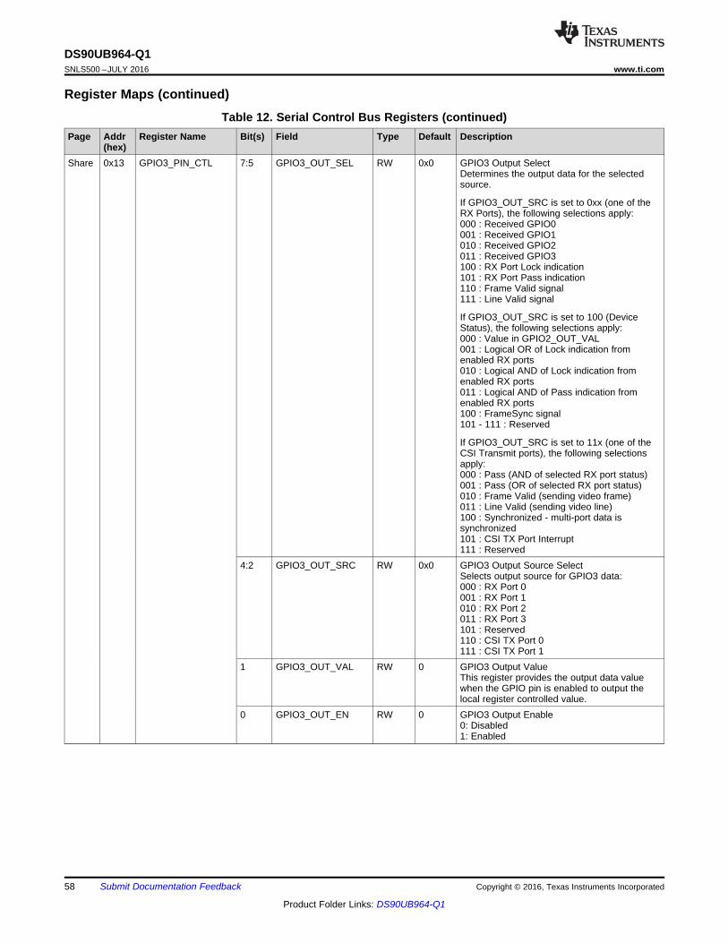
58
DS90UB964-Q1SNLS500 –JULY 2016 www.ti.com
Product Folder Links: DS90UB964-Q1
Submit Documentation Feedback Copyright © 2016, Texas Instruments Incorporated
Register Maps (continued)Table 12. Serial Control Bus Registers (continued)
Page Addr(hex)
Register Name Bit(s) Field Type Default Description
Share 0x13 GPIO3_PIN_CTL 7:5 GPIO3_OUT_SEL RW 0x0 GPIO3 Output SelectDetermines the output data for the selectedsource.
If GPIO3_OUT_SRC is set to 0xx (one of theRX Ports), the following selections apply:000 : Received GPIO0001 : Received GPIO1010 : Received GPIO2011 : Received GPIO3100 : RX Port Lock indication101 : RX Port Pass indication110 : Frame Valid signal111 : Line Valid signal
If GPIO3_OUT_SRC is set to 100 (DeviceStatus), the following selections apply:000 : Value in GPIO2_OUT_VAL001 : Logical OR of Lock indication fromenabled RX ports010 : Logical AND of Lock indication fromenabled RX ports011 : Logical AND of Pass indication fromenabled RX ports100 : FrameSync signal101 - 111 : Reserved
If GPIO3_OUT_SRC is set to 11x (one of theCSI Transmit ports), the following selectionsapply:000 : Pass (AND of selected RX port status)001 : Pass (OR of selected RX port status)010 : Frame Valid (sending video frame)011 : Line Valid (sending video line)100 : Synchronized - multi-port data issynchronized101 : CSI TX Port Interrupt111 : Reserved
4:2 GPIO3_OUT_SRC RW 0x0 GPIO3 Output Source SelectSelects output source for GPIO3 data:000 : RX Port 0001 : RX Port 1010 : RX Port 2011 : RX Port 3101 : Reserved110 : CSI TX Port 0111 : CSI TX Port 1
1 GPIO3_OUT_VAL RW 0 GPIO3 Output ValueThis register provides the output data valuewhen the GPIO pin is enabled to output thelocal register controlled value.
0 GPIO3_OUT_EN RW 0 GPIO3 Output Enable0: Disabled1: Enabled

59
DS90UB964-Q1www.ti.com SNLS500 –JULY 2016
Product Folder Links: DS90UB964-Q1
Submit Documentation FeedbackCopyright © 2016, Texas Instruments Incorporated
Register Maps (continued)Table 12. Serial Control Bus Registers (continued)
Page Addr(hex)
Register Name Bit(s) Field Type Default Description
Share 0x14 GPIO4_PIN_CTL 7:5 GPIO4_OUT_SEL RW 0x0 GPIO4 Output SelectDetermines the output data for the selectedsource.
If GPIO4_OUT_SRC is set to 0xx (one of theRX Ports), the following selections apply:000 : Received GPIO0001 : Received GPIO1010 : Received GPIO2011 : Received GPIO3100 : RX Port Lock indication101 : RX Port Pass indication110 : Frame Valid signal111 : Line Valid signal
If GPIO4_OUT_SRC is set to 100 (DeviceStatus), the following selections apply:000 : Value in GPIO2_OUT_VAL001 : Logical OR of Lock indication fromenabled RX ports010 : Logical AND of Lock indication fromenabled RX ports011 : Logical AND of Pass indication fromenabled RX ports100 : FrameSync signal101 - 111 : Reserved
If GPIO4_OUT_SRC is set to 11x (one of theCSI Transmit ports), the following selectionsapply:000 : Pass (AND of selected RX port status)001 : Pass (OR of selected RX port status)010 : Frame Valid (sending video frame)011 : Line Valid (sending video line)100 : Synchronized - multi-port data issynchronized101 : CSI TX Port Interrupt111 : Reserved
4:2 GPIO4_OUT_SRC RW 0x0 GPIO4 Output Source SelectSelects output source for GPIO4 data:000 : RX Port 0001 : RX Port 1010 : RX Port 2011 : RX Port 3100 : Device Status101 : Reserved110 : CSI TX Port 0111 : CSI TX Port 1
1 GPIO4_OUT_VAL RW 0 GPIO4 Output ValueThis register provides the output data valuewhen the GPIO pin is enabled to output thelocal register controlled value.
0 GPIO4_OUT_EN RW 0 GPIO4 Output Enable0: Disabled1: Enabled

60
DS90UB964-Q1SNLS500 –JULY 2016 www.ti.com
Product Folder Links: DS90UB964-Q1
Submit Documentation Feedback Copyright © 2016, Texas Instruments Incorporated
Register Maps (continued)Table 12. Serial Control Bus Registers (continued)
Page Addr(hex)
Register Name Bit(s) Field Type Default Description
Share 0x15 GPIO5_PIN_CTL 7:5 GPIO5_OUT_SEL RW 0x0 GPIO5 Output SelectDetermines the output data for the selectedsource.
If GPIO5_OUT_SRC is set to 0xx (one of theRX Ports), the following selections apply:000 : Received GPIO0001 : Received GPIO1010 : Received GPIO2011 : Received GPIO3100 : RX Port Lock indication101 : RX Port Pass indication110 : Frame Valid signal111 : Line Valid signal
If GPIO5_OUT_SRC is set to 100 (DeviceStatus), the following selections apply:000 : Value in GPIO5_OUT_VAL001 : Logical OR of Lock indication fromenabled RX ports010 : Logical AND of Lock indication fromenabled RX ports011 : Logical AND of Pass indication fromenabled RX ports100 : FrameSync signal101 - 111 : Reserved
If GPIO5_OUT_SRC is set to 11x (one of theCSI Transmit ports), the following selectionsapply:000 : Pass (AND of selected RX port status)001 : Pass (OR of selected RX port status)010 : Frame Valid (sending video frame)011 : Line Valid (sending video line)100 : Synchronized - multi-port data issynchronized101 : CSI TX Port Interrupt111 : Reserved
4:2 GPIO5_OUT_SRC RW 0x0 GPIO5 Output Source SelectSelects output source for GPIO5 data:000 : RX Port 0001 : RX Port 1010 : RX Port 2011 : RX Port 3100 : Device Status101 : Reserved110 : CSI TX Port 0111 : CSI TX Port 1
1 GPIO5_OUT_VAL RW 0 GPIO5 Output ValueThis register provides the output data valuewhen the GPIO pin is enabled to output thelocal register controlled value.
0 GPIO5_OUT_EN RW 0 GPIO5 Output Enable0: Disabled1: Enabled

61
DS90UB964-Q1www.ti.com SNLS500 –JULY 2016
Product Folder Links: DS90UB964-Q1
Submit Documentation FeedbackCopyright © 2016, Texas Instruments Incorporated
Register Maps (continued)Table 12. Serial Control Bus Registers (continued)
Page Addr(hex)
Register Name Bit(s) Field Type Default Description
Share 0x16 GPIO6_PIN_CTL 7:5 GPIO6_OUT_SEL RW 0x0 GPIO6 Output SelectDetermines the output data for the selectedsource.
If GPIO6_OUT_SRC is set to 0xx (one of theRX Ports), the following selections apply:000 : Received GPIO0001 : Received GPIO1010 : Received GPIO2011 : Received GPIO3100 : RX Port Lock indication101 : RX Port Pass indication110 : Frame Valid signal111 : Line Valid signal
If GPIO6_OUT_SRC is set to 100 (DeviceStatus), the following selections apply:000 : Value in GPIO6_OUT_VAL001 : Logical OR of Lock indication fromenabled RX ports010 : Logical AND of Lock indication fromenabled RX ports011 : Logical AND of Pass indication fromenabled RX ports100 : FrameSync signal101 - 111 : Reserved
If GPIO6_OUT_SRC is set to 11x (one of theCSI Transmit ports), the following selectionsapply:000 : Pass (AND of selected RX port status)001 : Pass (OR of selected RX port status)010 : Frame Valid (sending video frame)011 : Line Valid (sending video line)100 : Synchronized - multi-port data issynchronized101 : CSI TX Port Interrupt111 : Reserved
4:2 GPIO6_OUT_SRC RW 0x0 GPIO6 Output Source SelectSelects output source for GPIO6 data:000 : RX Port 0001 : RX Port 1010 : RX Port 2011 : RX Port 3100 : Device Status101 : Reserved110 : CSI TX Port 0111 : CSI TX Port 1
1 GPIO6_OUT_VAL RW 0 GPIO6 Output ValueThis register provides the output data valuewhen the GPIO pin is enabled to output thelocal register controlled value.
0 GPIO6_OUT_EN RW 0 GPIO6 Output Enable0: Disabled1: Enabled

62
DS90UB964-Q1SNLS500 –JULY 2016 www.ti.com
Product Folder Links: DS90UB964-Q1
Submit Documentation Feedback Copyright © 2016, Texas Instruments Incorporated
Register Maps (continued)Table 12. Serial Control Bus Registers (continued)
Page Addr(hex)
Register Name Bit(s) Field Type Default Description
Share 0x17 GPIO7_PIN_CTL 7:5 GPIO7_OUT_SEL RW 0x0 GPIO7 Output SelectDetermines the output data for the selectedsource.
If GPIO7_OUT_SRC is set to 0xx (one of theRX Ports), the following selections apply:000 : Received GPIO0001 : Received GPIO1010 : Received GPIO2011 : Received GPIO3100 : RX Port Lock indication101 : RX Port Pass indication110 : Frame Valid signal111 : Line Valid signal
If GPIO7_OUT_SRC is set to 100 (DeviceStatus), the following selections apply:000 : Value in GPIO7_OUT_VAL001 : Logical OR of Lock indication fromenabled RX ports010 : Logical AND of Lock indication fromenabled RX ports011 : Logical AND of Pass indication fromenabled RX ports100 : FrameSync signal101 - 111 : Reserved
If GPIO7_OUT_SRC is set to 11x (one of theCSI Transmit ports), the following selectionsapply:000 : Pass (AND of selected RX port status)001 : Pass (OR of selected RX port status)010 : Frame Valid (sending video frame)011 : Line Valid (sending video line)100 : Synchronized - multi-port data issynchronized101 : CSI TX Port Interrupt111 : Reserved
4:2 GPIO7_OUT_SRC RW 0x0 GPIO7 Output Source SelectSelects output source for GPIO7 data:000 : RX Port 0001 : RX Port 1010 : RX Port 2011 : RX Port 3100 : Device Status101 : Reserved110 : CSI TX Port 0111 : CSI TX Port 1
1 GPIO7_OUT_VAL RW 0 GPIO7 Output ValueThis register provides the output data valuewhen the GPIO pin is enabled to output thelocal register controlled value.
0 GPIO7_OUT_EN RW 0 GPIO7 Output Enable0: Disabled1: Enabled

63
DS90UB964-Q1www.ti.com SNLS500 –JULY 2016
Product Folder Links: DS90UB964-Q1
Submit Documentation FeedbackCopyright © 2016, Texas Instruments Incorporated
Register Maps (continued)Table 12. Serial Control Bus Registers (continued)
Page Addr(hex)
Register Name Bit(s) Field Type Default Description
Share 0x18 FS_CTL 7:4 FS_MODE RW 0x0 FrameSync Mode0000: Internal Generated FrameSync, useBack-channel frame clock from port 00001: Internal Generated FrameSync, useBack-channel frame clock from port 10010: Internal Generated FrameSync, useBack-channel frame clock from port 20011: Internal Generated FrameSync, useBack-channel frame clock from port 301xx: Internal Generated FrameSync, use25MHz clock1000: External FrameSync from GPIO01001: External FrameSync from GPIO11010: External FrameSync from GPIO21011: External FrameSync from GPIO31100: External FrameSync from GPIO41101: External FrameSync from GPIO51110: External FrameSync from GPIO61111: External FrameSync from GPIO7
3 FS_SINGLE RW/SC 0 Generate Single FrameSync pulseWhen this bit is set, a single FrameSync pulseis generated. The system should wait for thefull duration of the desired pulse beforegenerating another pulse. When using thisfeature, the FS_GEN_ENABLE bit shouldremain set to 0. This bit is self-clearing and willalways return 0.
2 FS_INIT_STATE RW 0 Initial StateThis register controls the initial state of theFrameSync signal.0: FrameSync initial state is 01: FrameSync initial state is 1
1 FS_GEN_MODE RW 0 FrameSync Generation ModeThis control selects between Hi/Lo and 50/50modes. In Hi/Lo mode, the FrameSyncgenerator will use the FS_HIGH_TIME andFS_LOW_TIME register values to separatelycontrol the High and Low periods for thegenerated FrameSync signal. In 50/50 mode,the FrameSync generator will use the values inthe FS_HIGH_TIME_0, FS_LOW_TIME_1 andFS_LOW_TIME_0 registers as a 24-bit valuefor both the High and Low periods of thegenerated FrameSync signal.0: Hi/Lo1: 50/50
0 FS_GEN_ENABLE RW 0 FrameSync Generation Enable0: Disabled1: Enabled
Share 0x19 FS_HIGH_TIME_1 7:0 FRAMESYNC_HIGH_TIME_1
RW 0x0 FrameSync High Time bits 15:8The value programmed to the FS_HIGH_TIMEregister should be reduced by 1 from thedesired delay. For example, a value of 0 in theFRAMESYNC_HIGH_TIME field will result in a1 cycle high pulse on the FrameSync signal.
Share 0x1A FS_HIGH_TIME_0 7:0 FRAMESYNC_HIGH_TIME_0
RW 0x0 FrameSync High Time bits 7:0The value programmed to the FS_HIGH_TIMEregister should be reduced by 1 from thedesired delay. For example, a value of 0 in theFRAMESYNC_HIGH_TIME field will result in a1 cycle high pulse on the FrameSync signal.

64
DS90UB964-Q1SNLS500 –JULY 2016 www.ti.com
Product Folder Links: DS90UB964-Q1
Submit Documentation Feedback Copyright © 2016, Texas Instruments Incorporated
Register Maps (continued)Table 12. Serial Control Bus Registers (continued)
Page Addr(hex)
Register Name Bit(s) Field Type Default Description
Share 0x1B FS_LOW_TIME_1 7:0 FRAMESYNC_LOW_TIME_1
RW 0x0 FrameSync Low Time bits 15:8The value programmed to the FS_HIGH_TIMEregister should be reduced by 1 from thedesired delay. For example, a value of 0 in theFRAMESYNC_HIGH_TIME field will result in a1 cycle high pulse on the FrameSync signal.
Share 0x1C FS_LOW_TIME_0 7:0 FRAMESYNC_LOW_TIME_0
RW 0x0 FrameSync Low Time bits 7:0The value programmed to the FS_HIGH_TIMEregister should be reduced by 1 from thedesired delay. For example, a value of 0 in theFRAMESYNC_HIGH_TIME field will result in a1 cycle high pulse on the FrameSync signal.
Share 0x1D MAX_FRM_HI 7:0 MAX_FRAME_HI RW 0x0 CSI-2 Maximum Frame Count bits 15:8In RAW mode operation, the FPD3 Receiverwill create CSI-2 video frames. For the FrameStart and Frame End packets of each videoframe, a 16-bit frame number field isgenerated. If the Maximum Frame Count valueis set to 0, the frame number is disabled andwill always be 0. If Maximum Frame Countvalue is non-zero, the frame number willincrement for each from 1 up to the MaximumFrame Count value before resetting to 1.
Share 0x1E MAX_FRM_LO 7:0 MAX_FRAME_LO RW 0x04 CSI-2 Maximum Frame Count bits 7:0In RAW mode operation, the FPD3 Receiverwill create CSI-2 video frames. For the FrameStart and Frame End packets of each videoframe, a 16-bit frame number field isgenerated. If the Maximum Frame Count valueis set to 0, the frame number is disabled andwill always be 0. If Maximum Frame Countvalue is non-zero, the frame number willincrement for each from 1 up to the MaximumFrame Count value before resetting to 1.
Share 0x1F CSI_PLL_CTL 7:3 RESERVED R 0x0 Reserved2 RESERVED RW 0 Reserved1:0 CSI_TX_SPEED RW 10 CSI Transmitter Speed select:
(See CSI-2 Transmitter Frequency)Controls the CSI Transmitter frequency.00 : 1.5 / 1.6 Gbps serial rate01 :Reserved10 : 800 Mbps serial rate11 : 400 Mbps serial rate
Share 0x20 FWD_CTL1 7 FWD_PORT3_DIS RW 1 Disable forwarding of RX Port 30: Forwarding enabled1: Forwarding disabled
6 FWD_PORT2_DIS RW 1 Disable forwarding of RX Port 20: Forwarding enabled1: Forwarding disabled
5 FWD_PORT1_DIS RW 1 Disable forwarding of RX Port 10: Forwarding enabled1: Forwarding disabled
4 FWD_PORT0_DIS RW 1 Disable forwarding of RX Port 00: Forwarding enabled1: Forwarding disabled
3 RX3_MAP RW 0 Map RX Port 3 to CSI-2 Port0: CSI-2 Port 01: CSI-2 Port 1It is recommended to disable forwarding for aport before changing the port mapping

65
DS90UB964-Q1www.ti.com SNLS500 –JULY 2016
Product Folder Links: DS90UB964-Q1
Submit Documentation FeedbackCopyright © 2016, Texas Instruments Incorporated
Register Maps (continued)Table 12. Serial Control Bus Registers (continued)
Page Addr(hex)
Register Name Bit(s) Field Type Default Description
2 RX2_MAP RW 0 Map RX Port 2 to CSI-2 Port0: CSI-2 Port 01: CSI-2 Port 1It is recommended to disable forwarding for aport before changing the port mapping
1 RX1_MAP RW 0 Map RX Port 1 to CSI-2 Port0: CSI-2 Port 01: CSI-2 Port 1It is recommended to disable forwarding for aport before changing the port mapping
0 RX0_MAP RW 0 Map RX Port 0 to CSI-2 Port0: CSI-2 Port 01: CSI-2 Port 1It is recommended to disable forwarding for aport before changing the port mapping
Share 0x21 FWD_CTL2 7 CSI_REPLICATE RW 0 CSI Replicate ModeWhen set to a 1, the CSI output from port 0 willalso be generated on CSI port 1. The sameoutput data is presented on both ports.
6 FWD_SYNC_AS_AVAIL
RW 0 Synchronized Forwarding As AvailableDuring Synchronized Forwarding, eachforwarding engine will wait for video data to beavailable from each enabled port, prior tosending the video line. Setting this bit to a 1will allow sending the next video line as itbecomes available. For example if RX Ports 0and 1 are being forwarded, port 0 video line isforwarded when it becomes available, ratherthan waiting until both ports 0 and ports 1 havevideo data available. This operation mayreduce the likelihood of buffer overflow errorsin some conditions. This bit will have no affectin video line concatenation mode and onlyaffects video lines (long packets) rather thansynchronization packets.This bit applies to both CSI output ports
5:4 CSI1_SYNC_FWD RW 0x0 Enable synchronized forwarding for CSI outputport 1 (See Synchronized Forwarding)00: Synchronized forwarding disabled01: Basic Synchronized forwarding enabled10: Synchronous forwarding with lineinterleaving11: Synchronous forwarding with lineconcatenationOnly one of CSI1_RR_FWD andCSI1_SYNC_FWD must be enabled at a time.
3:2 CSI0_SYNC_FWD RW 0x0 Enable synchronized forwarding for CSI outputport 0 ( Synchronized Forwarding)00: Synchronized forwarding disabled01: Basic Synchronized forwarding enabled10: Synchronous forwarding with lineinterleaving11: Synchronous forwarding with lineconcatenationOnly one of CSI0_RR_FWD andCSI0_SYNC_FWD must be enabled at a time.

66
DS90UB964-Q1SNLS500 –JULY 2016 www.ti.com
Product Folder Links: DS90UB964-Q1
Submit Documentation Feedback Copyright © 2016, Texas Instruments Incorporated
Register Maps (continued)Table 12. Serial Control Bus Registers (continued)
Page Addr(hex)
Register Name Bit(s) Field Type Default Description
1 CSI1_RR_FWD RW 1 Enable best-effort forwarding for CSI outputport 1.When this mode is enabled, no attempt ismade to synchronize the video traffic. Whenmultiple sources have data available toforward, the data will tend to be forwarded in around-robin fashion.0: Round robin forwarding disabled1: Round robin forwarding enabledOnly one of CSI1_RR_FWD andCSI1_SYNC_FWD must be enabled at a time.
0 CSI0_RR_FWD RW 1 Enable best-effort forwarding for CSI outputport 0.When this mode is enabled, no attempt ismade to synchronize the video traffic. Whenmultiple sources have data available toforward, the data will tend to be forwarded in around-robin fashion.0: Round robin forwarding disabled1: Round robin forwarding enabledOnly one of CSI0_RR_FWD andCSI0_SYNC_FWD must be enabled at a time.
Share 0x22 FWD_STS 7:4 RESERVED R 0x0 Reserved3 FWD_SYNC_FAIL1 R/COR 0 Forwarding synchronization failed for CSI
output port 1During Synchronized forwarding, this flagindicates a failure of synchronized video hasbeen detected. For this bit to be set, theforwarding process must have previously beensuccessful at sending at least onesynchronized video frame.0: No failure1: Synchronization failureThis bit is cleared on read.
2 FWD_SYNC_FAIL0 R/COR 0 Forwarding synchronization failed for CSIoutput port 0 During Synchronized forwarding,this flag indicates a failure of synchronizedvideo has been detected. For this bit to be set,the forwarding process must have previouslybeen successful at sending at least onesynchronized video frame.0: No failure1: Synchronization failureThis bit is cleared on read.
1 FWD_SYNC1 R 0 Forwarding synchronized for CSI output port 1During Synchronized forwarding, this bitindicates that the forwarding engine is currentlyable to provide synchronized video fromenabled Receive ports. This bit will always be0 if Synchronized forwarding is disabled.0: Video is not synchronized1: Video is synchronized
0 FWD_SYNC0 R 0 Forwarding synchronized for CSI output port 0During Synchronized forwarding, this bitindicates that the forwarding engine is currentlyable to provide synchronized video fromenabled Receive ports. This bit will always be0 if Synchronized forwarding is disabled.0: Video is not synchronized1: Video is synchronized
Share 0x23 INTERRUPT_CTL 7 INT_EN RW 0 Global Interrupt Enable:Enables interrupt on the interrupt signal to thecontroller.

67
DS90UB964-Q1www.ti.com SNLS500 –JULY 2016
Product Folder Links: DS90UB964-Q1
Submit Documentation FeedbackCopyright © 2016, Texas Instruments Incorporated
Register Maps (continued)Table 12. Serial Control Bus Registers (continued)
Page Addr(hex)
Register Name Bit(s) Field Type Default Description
6 RESERVED R 0 Reserved5 IE_CSI_TX1 RW 0 CSI Transmit Port 1 Interrupt:
Enable interrupt from CSI Transmitter Port 1.4 IE_CSI_TX0 RW 0 CSI Transmit Port 1 Interrupt:
Enable interrupt from CSI Transmitter Port 0.3 IE_RX3 RW 0 RX Port 3 Interrupt:
Enable interrupt from Receiver Port 3.2 IE_RX2 RW 0 RX Port 2 Interrupt:
Enable interrupt from Receiver Port 2.1 IE_RX1 RW 0 RX Port 1 Interrupt:
Enable interrupt from Receiver Port 1.0 IE_RX0 RW 0 RX Port 0 Interrupt:
Enable interrupt from Receiver Port 0.Share 0x24 INTERRUPT_STS 7 INT R 0 Global Interrupt:
Set if any enabled interrupt is indicated in theindividual status bits in this register. Thesetting of this bit is not dependent on theINT_EN bit in the INTERRUPT_CTL registerbut does depend on the IE_xxx bits. Forexample, if IE_RX0 and IS_RX0 are bothasserted, the INT bit is set to 1.
6 RESERVED R 0 Reserved5 IS_CSI_TX1 R 0 CSI Transmit Port 1 Interrupt:
An interrupt has occurred for CSI TransmitterPort 1. This interrupt is cleared upon readingthe CSI_TX_ISR register for CSI Transmit Port1.
4 IS_CSI_TX0 R 0 CSI Transmit Port 0 Interrupt:An interrupt has occurred for CSI TransmitterPort 0. This interrupt is cleared upon readingthe CSI_TX_ISR register for CSI Transmit Port0.
3 IS_RX3 R 0 RX Port 3 Interrupt:This interrupt is cleared by reading theassociated status register(s) for the event(s)that caused the interrupt. The status registersare RX_PORT_STS1, RX_PORT_STS2, andCSI_RX_STS.
2 IS_RX2 R 0 RX Port 2 Interrupt:An interrupt has occurred for Receive Port 2.This interrupt is cleared by reading theassociated status register(s) for the event(s)that caused the interrupt. The status registersare RX_PORT_STS1, RX_PORT_STS2, andCSI_RX_STS.
1 IS_RX1 R 0 RX Port 1 Interrupt:0x An interrupt has occurred for Receive Port1. This interrupt is cleared by reading theassociated status register(s) for the event(s)that caused the interrupt. The status registersare RX_PORT_STS1, RX_PORT_STS2, andCSI_RX_STS.
0 IS_RX0 R 0 RX Port 0 Interrupt:An interrupt has occurred for Receive Port 0.This interrupt is cleared by reading theassociated status register(s) for the event(s)that caused the interrupt. The status registersare RX_PORT_STS1, RX_PORT_STS2, andCSI_RX_STS.

68
DS90UB964-Q1SNLS500 –JULY 2016 www.ti.com
Product Folder Links: DS90UB964-Q1
Submit Documentation Feedback Copyright © 2016, Texas Instruments Incorporated
Register Maps (continued)Table 12. Serial Control Bus Registers (continued)
Page Addr(hex)
Register Name Bit(s) Field Type Default Description
Share 0x25 TS_CONFIG 7 RESERVED R 0 Reserved6 FS_POLARITY RW 0 Framesync Polarity
Indicates active edge of FrameSync signal0: Rising edge1: Falling edge
5:4 TS_RES_CTL RW 0x0 Timestamp Resolution Control00: 40 ns01: 80 ns10: 160 ns11: 1.0 us
3 TS_AS_AVAIL RW 0 Timestamp Ready Control0: Normal operation1: Indicate timestamps ready as soon as allport timestamps are available
2 RESERVED R 0 Reserved1 TS_FREERUN RW 0 FreeRun Mode
0: FrameSync mode1: FreeRun mode
0 TS_MODE RW 0 Timestamp Mode0: Line start1: Frame start
Share 0x26 TS_CONTROL 7:5 RESERVED R 0x0 Reserved4 TS_FREEZE RW 0 Freeze Timestamps
0: Normal operation1: Freeze timestampsSetting this bit will freeze timestamps and clearthe TS_READY flag. The TS_FREEZE bitshould be cleared after reading timestamps toresume operation.
3 TS_ENABLE3 RW 0 Timestamp Enable RX Port 30: Disabled1: Enabled
2 TS_ENABLE2 RW 0 Timestamp Enable RX Port 20: Disabled1: Enabled
1 TS_ENABLE1 RW 0 Timestamp Enable RX Port 10: Disabled1: Enabled
0 TS_ENABLE0 RW 0 Timestamp Enable RX Port 00: Disabled1: Enabled
Share 0x27 TS_LINE_HI 7:0 TS_LINE_HI RW 0x0 Timestamp Line, upper 8 bitsThis field is the line number at which to capturethe timestamp when Line Start mode isenabled. For proper operation, the line numbershould be set to a value greater than 1.During Frame Start mode, if TS_FREERUN isset, the TS_LINE value is used to determinewhen to begin checking for Frame Start
Share 0x28 TS_LINE_LO 7:0 TS_LINE_LO RW 0x0 Timestamp Line, lower 8 bitsThis field is the line number at which to capturethe timestamp when Line Start mode isenabled. For proper operation, the line numbershould be set to a value greater than 1.During Frame Start mode, if TS_FREERUN isset, the TS_LINE value is used to determinewhen to begin checking for Frame Start
Share 0x29 TS_STATUS 7:5 RESERVED R 0x0 Reserved

69
DS90UB964-Q1www.ti.com SNLS500 –JULY 2016
Product Folder Links: DS90UB964-Q1
Submit Documentation FeedbackCopyright © 2016, Texas Instruments Incorporated
Register Maps (continued)Table 12. Serial Control Bus Registers (continued)
Page Addr(hex)
Register Name Bit(s) Field Type Default Description
4 TS_READY R 0 Timestamp ReadyThis flag indicates when timestamps are readyto be read. This flag is cleared when theTS_FREEZE bit is set.
3 TS_VALID3 R 0 Timestamp Valid, RX Port 32 TS_VALID2 R 0 Timestamp Valid, RX Port 21 TS_VALID1 R 0 Timestamp Valid, RX Port 10 TS_VALID0 R 0 Timestamp Valid, RX Port 0
Share 0x2A TIMESTAMP_P0_HI 7:0 TIMESTAMP_P0_HI R 0x0 Timestamp, upper 8 bits, RX Port 0Share 0x2B TIMESTAMP_P0_LO 7:0 TIMESTAMP_P0_LO R 0x0 Timestamp, lower 8 bits, RX Port 0Share 0x2C TIMESTAMP_P1_HI 7:0 TIMESTAMP_P1_HI R 0x0 Timestamp, upper 8 bits, RX Port 1Share 0x2D TIMESTAMP_P1_LO 7:0 TIMESTAMP_P1_LO R 0x0 Timestamp, lower 8 bits, RX Port 1Share 0x2E TIMESTAMP_P2_HI 7:0 TIMESTAMP_P2_HI R 0x0 Timestamp, upper 8 bits, RX Port 2Share 0x2F TIMESTAMP_P2_LO 7:0 TIMESTAMP_P2_LO R 0x0 Timestamp, lower 8 bits, RX Port 2Share 0x30 TIMESTAMP_P3_HI 7:0 TIMESTAMP_P3_HI R 0x0 Timestamp, upper 8 bits, RX Port 3Share 0x31 TIMESTAMP_P3_LO 7:0 TIMESTAMP_P3_LO R 0x0 Timestamp, lower 8 bits, RX Port 3Share 0x32 CSI_PORT_SEL 7:5 RESERVED R 0x0 Reserved
4 TX_READ_PORT RW 0 Select TX port for register readThis field selects one of the two TX portregister blocks for readback. This applies tothe subsequent registers prefixed "CSI".0: Port 0 registers1: Port 1 registers
3:2 RESERVED R 0x0 Reserved1 TX_WRITE_PORT_1 RW 0 Write Enable for TX port 1 registers
This bit enables writes to TX port 1 registers.Any combination of TX port registers can bewritten simultaneously. This applies to thesubsequent registers prefixed "CSI".0: Writes disabled1: Writes enabled
0 TX_WRITE_PORT_0 RW 0 Write Enable for TX port 0 registersThis bit enables writes to TX port 0 registers.Any combination of TX port registers can bewritten simultaneously. This applies to thesubsequent registers prefixed "CSI".0: Writes disabled1: Writes enabled
CSI 0x33 CSI_CTL 7 RESERVED R 0 Reserved6 CSI_CAL_EN RW 0 Enable initial CSI Skew-Calibration sequence
When the initial skew-calibration sequence isenabled, the CSI Transmitter will send thesequence at initialization, prior to sending anyHS data. This bit should be set when operatingat 1.6 Gbps CSI speed (as configured in theCSI_PLL register).0: Disabled1: Enabled
5:4 CSI_LANE_COUNT RW 0x0 CSI lane count00: 4 lanes01: 3 lanes10: 2 lanes11: 1 lane

70
DS90UB964-Q1SNLS500 –JULY 2016 www.ti.com
Product Folder Links: DS90UB964-Q1
Submit Documentation Feedback Copyright © 2016, Texas Instruments Incorporated
Register Maps (continued)Table 12. Serial Control Bus Registers (continued)
Page Addr(hex)
Register Name Bit(s) Field Type Default Description
3:2 CSI_ULP RW 0 Force LP00 state on data/clock lanes00: Normal operation01: LP00 state forced only on data lanes10: Reserved11: LP00 state forced on data and clock lanes
1 CSI_CONTS_CLOCK RW 0 Enable CSI continuous clock mode0: Disabled1: Enabled
0 CSI ENABLE RW 0 Enable CSI output0: Disabled1: Enabled
CSI 0x34 CSI_CTL2 7:4 RESERVED R 0x0 Reserved3 CSI_PASS_MODE RW 0 CSI PASS indication mode
Determines whether the CSI Pass indication isfor a single port or all enabled ports.0 : Assert PASS if at least one enabledReceive port is providing valid video data1 : Assert PASS only if ALL enabled Receiveports are providing valid video data
2 CSI_CAL_INV RW 0 CSI Calibration Inverted Data patternDuring the CSI skew-calibration pattern, theCSI Transmitter will send a sequence of01010101 data (first bit 0). Setting this bit to a1 will invert the sequence to 10101010 data.
1 CSI_CAL_SINGLE RW 0 Enable single periodic CSI Skew-CalibrationsequenceSetting this bit will send a single skew-calibration sequence from the CSI Transmitter.The skew-calibration sequence is the 1010 bitsequence required for periodic calibration. Thecalibration sequence is sent at the next idleperiod on the CSI interface. This bit is self-clearing and will reset to 0 after the calibrationsequence is sent.
0 CSI_CAL_PERIODIC RW 0 Enable periodic CSI Skew-CalibrationsequenceWhen the periodic skew-calibration sequenceis enabled, the CSI Transmitter will send theperiodic skew-calibration sequence followingthe sending of Frame End packets.0: Disabled1: Enabled
CSI 0x35 CSI_STS 7:5 RESERVED R 0x0 Reserved4 TX_PORT_NUM R 0 TX Port Number
This read-only field indicates the number of thecurrently selected TX read port.
3:2 RESERVED R 0x0 Reserved1 TX_PORT_SYNC R 0 TX Port Synchronized
This bit indicates the CSI Transmit Port is ableto properly synchronize input data streamsfrom multiple sources. This bit is 0 ifsynchronization is disabled via the FWD_CTL2register.0 : Input streams are not synchronized1 : Input streams are synchronized

71
DS90UB964-Q1www.ti.com SNLS500 –JULY 2016
Product Folder Links: DS90UB964-Q1
Submit Documentation FeedbackCopyright © 2016, Texas Instruments Incorporated
Register Maps (continued)Table 12. Serial Control Bus Registers (continued)
Page Addr(hex)
Register Name Bit(s) Field Type Default Description
0 TX_PORT_PASS R 0 TX Port PassIndicates valid data is available on at least oneport, or on all ports if configured for all portstatus via the CSI_PASS_MODE bit in theCSI_CTL2 register. The function differs basedon mode of operation.In asynchronous operation, theTX_PORT_PASS indicates the CSI port isactively delivering valid video data. The statusis cleared based on detection of an errorcondition that interrupts transmission.During Synchronized forwarding, theTX_PORT_PASS indicates valid data isavailable for delivery on the CSI TX output.Data may not be delivered if ports are notsynchronized. The TX_PORT_SYNC status isa better indicator that valid data is beingdelivered to the CSI transmit port.
CSI 0x36 CSI_TX_ICR 7:5 RESERVED R 0x0 Reserved4 IE_RX_PORT_INT RW 0 RX Port Interrupt Enable
Enable interrupt based on receiver portinterrupt for the RX Ports being forwarded tothe CSI Transmit Port.
3 IE_CSI_SYNC_ERROR
RW 0 CSI Sync Error interrupt EnableEnable interrupt on CSI Synchronizationenable.
2 IE_CSI_SYNC RW 0 CSI Synchronized interrupt EnableEnable interrupts on CSI Transmit Portassertion of CSI Synchronized Status.
1 IE_CSI_PASS_ERROR
RW 0 CSI RX Pass Error interrupt EnableEnable interrupt on CSI Pass Error
0 IE_CSI_PASS RW 0 CSI Pass interrupt EnableEnable interrupt on CSI Transmit Portassertion of CSI Pass.
CSI 0x37 CSI_TX_ISR 7:5 RESERVED R 0x0 Reserved4 IS_RX_PORT_INT R/COR 0 RX Port Interrupt
A Receiver port interrupt has been generatedfor one of the RX Ports being forwarded to theCSI Transmit Port. A read of the associatedport receive status registers will clear thisinterrupt. See the PORT_ISR_HI andPORT_ISR_LO registers for details.
3 IS_CSI_SYNC_ERROR
R/COR 0 CSI Sync Error interruptA synchronization error has been detected formultiple video stream inputs to the CSITransmitter.
2 IS_CSI_SYNC R/COR 0 CSI Synchronized interruptCSI Transmit Port assertion of CSISynchronized Status. Current status for CSISync can be read from the TX_PORT_SYNCflag in the CSI_STS register.
1 IS_CSI_PASS_ERROR
R/COR 0 CSI RX Pass Error interruptA deassertion of CSI Pass has been detectedon one of the RX Ports being forwarded to theCSI Transmit Port
0 IS_CSI_PASS R/COR 0 CSI Pass interruptCSI Transmit Port assertion of CSI Passdetected. Current status for the CSI Passindication can be read from theTX_PORT_PASS flag in the CSI_STS register

72
DS90UB964-Q1SNLS500 –JULY 2016 www.ti.com
Product Folder Links: DS90UB964-Q1
Submit Documentation Feedback Copyright © 2016, Texas Instruments Incorporated
Register Maps (continued)Table 12. Serial Control Bus Registers (continued)
Page Addr(hex)
Register Name Bit(s) Field Type Default Description
Share 0x42 AEQ_CTL 7 RESERVED R 0 Reserved6:4 AEQ_ERR_CTL 0x0 AEQ Error Control
Setting any of these bits will enable FPD3 errorchecking during the Adaptive Equalizationprocess. Errors are accumulated over 1/2 ofthe period of the timer set by theADAPTIVE_EQ_RELOCK_TIME filed in theAEQ_TEST register. If the number of errors isgreater than the programmed threshold(AEQ_ERR_THOLD), the AEQ will attempt toincrease the EQ setting. The errors may alsobe checked as part of EQ setting validation ifAEQ_2STEP_EN is set. The following errorsare checked based on this three bit field:[2] FPD3 clk1/clk0 errors[1] DCA sequence errors[0] Parity errors
3 RESERVED RW 0 Reserved2 AEQ_2STEP_EN RW 0 AEQ 2-step enable
This bit enables a two-step operation as part ofthe Adaptive EQ algorithm. If disabled, thestate machine will wait for a programmedperiod of time, then check status to determineif setting is valid. If enabled, the state machinewill wait for 1/2 the programmed period, thencheck for errors over an additional 1/2 theprogrammed period. If errors occur during the2nd step, the state machine will immediatelymove to the next setting.0 : Wait for full programmed delay, then checkinstantaneous lock value1 : Wait for 1/2 programmed time, then checkfor errors over 1/2 programmed time. Theprogrammed time is controlled by theADAPTIVE_EQ_RELOCK_TIME field in theAEQ_TEST register
1 AEQ_OUTER_LOOP RW 0 AEQ outer loop controlThis bit controls whether the Equalizer orSFILTER adaption is the outer loop when theAEQ adaption includes SFILTER adaption.0 : AEQ is inner loop, SFILTER is outer loop1 : AEQ is outer loop, SFILTER is inner loop
0 AEQ_SFILTER_EN RW 1 Enable SFILTER Adaption with AEQSetting this bit allows SFILTER adaption aspart of the Adaptive Equalizer algorithm.
Share 0x43 AEQ_ERR_THOLD 7:0 AEQ_ERR_THRESHOLD
RW 0x1 AEQ Error ThresholdThis register controls the error threshold todetermine when to re-adapt the EQ settings.This register should not be programmed to avalue of 0.
Share 0x4C FPD3_PORT_SEL 7:6 PHYS_PORT_NUM R 0x0Port#
Physical port numberThis field provides the physical port connectionwhen reading from a remote device via the Bi-directional Control Channel.When accessed via local I2C interfaces, thevalue returned is always 0. When accessed viaBi-directional Control Channel, the valuereturned is the port number of the Receive portconnection.

73
DS90UB964-Q1www.ti.com SNLS500 –JULY 2016
Product Folder Links: DS90UB964-Q1
Submit Documentation FeedbackCopyright © 2016, Texas Instruments Incorporated
Register Maps (continued)Table 12. Serial Control Bus Registers (continued)
Page Addr(hex)
Register Name Bit(s) Field Type Default Description
5:4 RX_READ_PORT RW 0x0Port#
Select RX port for register readThis field selects one of the four RX portregister blocks for readback. This applies to allpaged FPD3 Receiver port registers.00: Port 0 registers01: Port 1 registers10: Port 2 registers11: Port 3 registersWhen accessed via local I2C interfaces, thedefault setting is 0. When accessed via Bi-directional Control Channel, the default valueis the port number of the Receive portconnection.
3 RX_WRITE_PORT_3 RW 01 forRX Port3
Write Enable for RX port 3 registersThis bit enables writes to RX port 3 registers.Any combination of RX port registers can bewritten simultaneously. This applies to allpaged FPD3 Receiver port registers.0: Writes disabled1: Writes enabledWhen accessed via Bi-directional ControlChannel, the default value is 1 if accessedover RX port 3.
2 RX_WRITE_PORT_2 RW 01 forRX Port2
Write Enable for RX port 2 registersThis bit enables writes to RX port 2 registers.Any combination of RX port registers can bewritten simultaneously. This applies to allpaged FPD3 Receiver port registers.0: Writes disabled1: Writes enabledWhen accessed via Bi-directional ControlChannel, the default value is 1 if accessedover RX port 2.
1 RX_WRITE_PORT_1 RW 01 forRX Port1
Write Enable for RX port 1 registersThis bit enables writes to RX port 1 registers.Any combination of RX port registers can bewritten simultaneously. This applies to allpaged FPD3 Receiver port registers.0: Writes disabled1: Writes enabledWhen accessed via Bi-directional ControlChannel, the default value is 1 if accessedover RX port 1.
0 RX_WRITE_PORT_0 RW 01 forRX Port0
Write Enable for RX port 0 registersThis bit enables writes to RX port 0 registers.Any combination of RX port registers can bewritten simultaneously. This applies to allpaged FPD3 Receiver port registers.0: Writes disabled1: Writes enabledWhen accessed via Bi-directional ControlChannel, the default value is 1 if accessedover RX port 0.
RX 0x4D RX_PORT_STS1 7:6 RX_PORT_NUM R 0x0 RX Port NumberThis read-only field indicates the number of thecurrently selected RX read port.
5 BCC_CRC_ERROR R/COR 0 Bi-directional Control Channel CRC ErrorDetectedThis bit indicates a CRC error has beendetected in the forward control channel. If thisbit is set, an error may have occurred in thecontrol channel operation. This bit is clearedon read.

74
DS90UB964-Q1SNLS500 –JULY 2016 www.ti.com
Product Folder Links: DS90UB964-Q1
Submit Documentation Feedback Copyright © 2016, Texas Instruments Incorporated
Register Maps (continued)Table 12. Serial Control Bus Registers (continued)
Page Addr(hex)
Register Name Bit(s) Field Type Default Description
4 LOCK_STS_CHG R/COR 0 Lock Status ChangedThis bit is set if a change in receiver lockstatus has been detected since the last read ofthis register. Current lock status is available inthe LOCK_STS bit of this registerThis bit is cleared on read.
3 BCC_SEQ_ERROR R/COR 0 Bi-directional Control Channel Sequence ErrorDetectedThis bit indicates a sequence error has beendetected in the forward control channel. If thisbit is set, an error may have occurred in thecontrol channel operation. This bit is clearedon read.
2 PARITY_ERROR R 0 FPD3 parity errors detectedThis flag is set when the number of parityerrors detected is greater than the thresholdprogrammed in the PAR_ERR_THOLDregisters.1: Number of FPD3 parity errors detected isgreater than the threshold0: Number of FPD3 parity errors is below thethreshold This bit is cleared when theRX_PAR_ERR_HI/LO registers are cleared.
1 PORT_PASS R 0 Receiver PASS indication This bit indicates thecurrent status of the Receiver PASS indication.The requirements for setting the ReceiverPASS indication are controlled by thePORT_PASS_CTL register.1: Receive input has met PASS criteria0: Receive input does not meet PASS criteria
0 LOCK_STS R 0 FPD-Link III receiver is locked to incoming data1: Receiver is locked to incoming data0: Receiver is not locked
RX 0x4E RX_PORT_STS2 7 LINE_LEN_UNSTABLE
R/COR 0 Line Length UnstableIf set, this bit indicates the line length wasdetected as unstable during a previous videoframe. The line length is considered to bestable if all the lines in the video frame havethe same length. This flag will remain set untilread.
6 LINE_LEN_CHG R/COR 0 Line Length Changed1: Change of line length detected0: Change of line length not detected This bit iscleared on read.
5 FPD3_ENCODE_ERROR
R/COR 0 FPD3 Encoder error detectedIf set, this flag indicates an error in the FPD-Link III encoding has been detected by theFPD-Link III receiver.This bit is cleared on read.Note, to detect FP3 Encoder errors, theLINK_ERROR_COUNT must be enabled witha LINK_ERR_THRESH value greater than 1.Otherwise, the loss of Receiver Lock willprevent detection of the Encoder error.
4 BUFFER_ERROR R/COR 0 Packet buffer error detected. If this bit is set,an overflow condition has occurred on thepacket buffer FIFO.1: Packet Buffer error detected0: No Packet Buffer errors detectedThis bit is cleared on read.
3 RESERVED R 0 Reserved

75
DS90UB964-Q1www.ti.com SNLS500 –JULY 2016
Product Folder Links: DS90UB964-Q1
Submit Documentation FeedbackCopyright © 2016, Texas Instruments Incorporated
Register Maps (continued)Table 12. Serial Control Bus Registers (continued)
Page Addr(hex)
Register Name Bit(s) Field Type Default Description
2 FREQ_STABLE R 0 Frequency measurement stable1 NO_FPD3_CLK R 0 No FPD-Link III input clock detected0 LINE_CNT_CHG R/COR 0 Line Count Changed
1: Change of line count detected0: Change of line count not detectedThis bit is cleared on read.
RX 0x4F RX_FREQ_HIGH 7:0 FREQ_CNT_HIGH R 0x0 Frequency Counter High Byte (MHz)The Frequency counter reports the measuredfrequency for the FPD3 Receiver. This portionof the field is the integer value in MHz.
RX 0x50 RX_FREQ_LOW 7:0 FREQ_CNT_LOW R 0x0 Frequency Counter Low Byte (1/256 MHz)The Frequency counter reports the measuredfrequency for the FPD3 Receiver. This portionof the field is the fractional value in 1/256 MHz.
RX 0x55 RX_PAR_ERR_HI 7:0 PAR ERROR BYTE 1 R 0x0 Number of FPD3 parity errors – 8 mostsignificant bitsThe parity error counter registers return thenumber of data parity errors that have beendetected on the FPD3 Receiver data since thelast detection of valid lock or last read of theRX_PAR_ERR_LO register. For accuratereading of the parity error count, disable theRX PARITY CHECKER ENABLE bit in register0x2 prior to reading the parity error countregisters. This register is cleared upon readingthe RX_PAR_ERR_LO register.
RX 0x56 RX_PAR_ERR_LO 7:0 PAR ERROR BYTE 0 R 0x0 Number of FPD3 parity errors – 8 leastsignificant bitsThe parity error counter registers return thenumber of data parity errors that have beendetected on the FPD3 Receiver data since thelast detection of valid lock or last read of theRX_PAR_ERR_LO register. For accuratereading of the parity error count, disable theRX PARITY CHECKER ENABLE bit in register0x2 prior to reading the parity error countregisters. This register is cleared on read.
RX 0x57 BIST_ERR_COUNT 7:0 BIST ERRORCOUNT
R 0x0 Bist Error CountReturns BIST error count
RX 0x58 BCC_CONFIG 7 I2C PASSTHROUGH ALL
RW 0 I2C Pass-Through All Transactions0: Disabled1: Enabled
6 I2C PASSTHROUGH
RW 0 I2C Pass-Through to Serializer if decodematches0: Pass-Through Disabled1: Pass-Through Enabled
5 AUTO ACK ALL RW 0 Automatically Acknowledge all I2C writesindependent of the forward channel lock stateor status of the remote Acknowledge1: Enable0: Disable
4 BC_ALWAYS_ON RW 1 Back channel enable1: Back channel is always enabledindependent of I2C_PASS_THROUGH andI2C_PASS_THROUGH_ALL0: Back channel enable requires setting ofeither I2C_PASS_THROUGH andI2C_PASS_THROUGH_ALL This bit may onlybe written via a local I2C master.

76
DS90UB964-Q1SNLS500 –JULY 2016 www.ti.com
Product Folder Links: DS90UB964-Q1
Submit Documentation Feedback Copyright © 2016, Texas Instruments Incorporated
Register Maps (continued)Table 12. Serial Control Bus Registers (continued)
Page Addr(hex)
Register Name Bit(s) Field Type Default Description
3 BC CRCGENERATORENABLE
RW 1 Back Channel CRC Generator Enable0: Disable1: Enable
2:0 BC FREQ SELECT RW,Strap
0x0 Back Channel Frequency Select000: 2.5 Mbps (default forDS90UB913AQ/913Q/933Q compatibility)001: 1.5625 Mbps010 - 111 : ReservedNote that changing this setting will result insome errors on the back channel for a shortperiod of time. If set over the control channel,the Deserializer should first be programmed toAuto-Ack operation to avoid a control channeltimeout due to lack of response from theSerializer.
RX 0x59 RESERVED 7:0 RESERVED RW 0x0 ReservedRX 0x5A RESERVED 7:0 RESERVED RW 0x0 ReservedRX 0x5B SER_ID 7:1 SER ID RW 0x0 Remote Serializer ID
This field is normally loaded automatically fromthe remote Serializer.
0 FREEZE DEVICE ID RW 0 Freeze Serializer Device IDPrevent auto-loading of the Serializer DeviceID from the Forward Channel. The ID is frozenat the value written.
RX 0x5C SER_ALIAS_ID 7:1 SER ALIAS ID RW 0x0 7-bit Remote Serializer Alias IDConfigures the decoder for detectingtransactions designated for an I2C Slavedevice attached to the remote Deserializer.The transaction is remapped to the addressspecified in the Slave ID register. A value of 0in this field disables access to the remote I2CSlave.
0 SER AUTO ACK RW 0 Automatically Acknowledge all I2C writes tothe remote Serializer independent of theforward channel lock state or status of theremote Serializer Acknowledge1: Enable0: Disable
RX 0x5D SlaveID[0] 7:1 SLAVE ID0 RW 0x0 7-bit Remote Slave Device ID 0Configures the physical I2C address of theremote I2C Slave device attached to theremote Serializer. If an I2C transaction isaddressed to the Slave Alias ID0, thetransaction is remapped to this address beforepassing the transaction across the Bi-directional Control Channel to the Serializer.
0 RESERVED R 0 Reserved.RX 0x5E SlaveID[1] 7:1 SLAVE ID1 RW 0x0 7-bit Remote Slave Device ID 1
Configures the physical I2C address of theremote I2C Slave device attached to theremote Serializer. If an I2C transaction isaddressed to the Slave Alias ID1, thetransaction is remapped to this address beforepassing the transaction across the Bi-directional Control Channel to the Serializer.
0 RESERVED R 0 Reserved.

77
DS90UB964-Q1www.ti.com SNLS500 –JULY 2016
Product Folder Links: DS90UB964-Q1
Submit Documentation FeedbackCopyright © 2016, Texas Instruments Incorporated
Register Maps (continued)Table 12. Serial Control Bus Registers (continued)
Page Addr(hex)
Register Name Bit(s) Field Type Default Description
RX 0x5F SlaveID[2] 7:1 SLAVE ID2 RW 0x0 7-bit Remote Slave Device ID 2Configures the physical I2C address of theremote I2C Slave device attached to theremote Serializer. If an I2C transaction isaddressed to the Slave Alias ID2, thetransaction is remapped to this address beforepassing the transaction across the Bi-directional Control Channel to the Serializer.
0 RESERVED R 0 Reserved.RX 0x60 SlaveID[3] 7:1 SLAVE ID3 RW 0x0 7-bit Remote Slave Device ID 3
Configures the physical I2C address of theremote I2C Slave device attached to theremote Serializer. If an I2C transaction isaddressed to the Slave Alias ID3, thetransaction is remapped to this address beforepassing the transaction across the Bi-directional Control Channel to the Serializer.
0 RESERVED R 0 Reserved.RX 0x61 SlaveID[4] 7:1 SLAVE ID4 RW 0x0 7-bit Remote Slave Device ID 4
Configures the physical I2C address of theremote I2C Slave device attached to theremote Serializer. If an I2C transaction isaddressed to the Slave Alias ID4, thetransaction is remapped to this address beforepassing the transaction across the Bi-directional Control Channel to the Serializer.
0 RESERVED R 0 Reserved.RX 0x62 SlaveID[5] 7:1 SLAVE ID5 RW 0x0 7-bit Remote Slave Device ID 5
Configures the physical I2C address of theremote I2C Slave device attached to theremote Serializer. If an I2C transaction isaddressed to the Slave Alias ID5, thetransaction is remapped to this address beforepassing the transaction across the Bi-directional Control Channel to the Serializer.
0 RESERVED R 0 Reserved.RX 0x63 SlaveID[6] 7:1 SLAVE ID6 RW 0x0 7-bit Remote Slave Device ID 6
Configures the physical I2C address of theremote I2C Slave device attached to theremote Serializer. If an I2C transaction isaddressed to the Slave Alias ID6, thetransaction is remapped to this address beforepassing the transaction across the Bi-directional Control Channel to the Serializer.
0 RESERVED R 0 Reserved.RX 0x64 SlaveID[7] 7:1 SLAVE ID7 RW 0x0 7-bit Remote Slave Device ID 7
Configures the physical I2C address of theremote I2C Slave device attached to theremote Serializer. If an I2C transaction isaddressed to the Slave Alias ID7, thetransaction is remapped to this address beforepassing the transaction across the Bi-directional Control Channel to the Serializer.
0 RESERVED R 0 Reserved.

78
DS90UB964-Q1SNLS500 –JULY 2016 www.ti.com
Product Folder Links: DS90UB964-Q1
Submit Documentation Feedback Copyright © 2016, Texas Instruments Incorporated
Register Maps (continued)Table 12. Serial Control Bus Registers (continued)
Page Addr(hex)
Register Name Bit(s) Field Type Default Description
RX 0x65 SlaveAlias[0] 7:1 SLAVE ALIAS ID0 RW 0x0 7-bit Remote Slave Device Alias ID 0Configures the decoder for detectingtransactions designated for an I2C Slavedevice attached to the remote Serializer. Thetransaction is remapped to the addressspecified in the Slave ID0 register. A value of 0in this field disables access to the remote I2CSlave.
0 SLAVE AUTO ACK 0 RW 0 Automatically Acknowledge all I2C writes tothe remote Slave 0 independent of the forwardchannel lock state or status of the remoteSerializer Acknowledge1: Enable0: Disable
RX 0x66 SlaveAlias[1] 7:1 SLAVE ALIAS ID1 RW 0x0 7-bit Remote Slave Device Alias ID 1Configures the decoder for detectingtransactions designated for an I2C Slavedevice attached to the remote Serializer. Thetransaction is remapped to the addressspecified in the Slave ID1 register. A value of 0in this field disables access to the remote I2CSlave.
0 SLAVE AUTO ACK 1 RW 0 Automatically Acknowledge all I2C writes tothe remote Slave 1 independent of the forwardchannel lock state or status of the remoteSerializer Acknowledge1: Enable0: Disable
RX 0x67 SlaveAlias[2] 7:1 SLAVE ALIAS ID2 RW 0x0 7-bit Remote Slave Device Alias ID 2Configures the decoder for detectingtransactions designated for an I2C Slavedevice attached to the remote Serializer. Thetransaction is remapped to the addressspecified in the Slave ID2 register. A value of 0in this field disables access to the remote I2CSlave.
0 SLAVE AUTO ACK 2 RW 0 Automatically Acknowledge all I2C writes tothe remote Slave 2 independent of the forwardchannel lock state or status of the remoteSerializer Acknowledge1: Enable0: Disable
RX 0x68 SlaveAlias[3] 7:1 SLAVE ALIAS ID3 RW 0x0 7-bit Remote Slave Device Alias ID 3Configures the decoder for detectingtransactions designated for an I2C Slavedevice attached to the remote Serializer. Thetransaction is remapped to the addressspecified in the Slave ID3 register. A value of 0in this field disables access to the remote I2CSlave.
0 SLAVE AUTO ACK 3 RW 0 Automatically Acknowledge all I2C writes tothe remote Slave 3 independent of the forwardchannel lock state or status of the remoteSerializer Acknowledge1: Enable0: Disable
RX 0x69 SlaveAlias[4] 7:1 SLAVE ALIAS ID4 RW 0x0 7-bit Remote Slave Device Alias ID 4Configures the decoder for detectingtransactions designated for an I2C Slavedevice attached to the remote Serializer. Thetransaction is remapped to the addressspecified in the Slave ID4 register. A value of 0in this field disables access to the remote I2CSlave.

79
DS90UB964-Q1www.ti.com SNLS500 –JULY 2016
Product Folder Links: DS90UB964-Q1
Submit Documentation FeedbackCopyright © 2016, Texas Instruments Incorporated
Register Maps (continued)Table 12. Serial Control Bus Registers (continued)
Page Addr(hex)
Register Name Bit(s) Field Type Default Description
0 SLAVE AUTO ACK 4 RW 0 Automatically Acknowledge all I2C writes tothe remote Slave 4 independent of the forwardchannel lock state or status of the remoteSerializer Acknowledge1: Enable0: Disable
RX 0x6A SlaveAlias[5] 7:1 SLAVE ALIAS ID5 RW 0x0 7-bit Remote Slave Device Alias ID 5Configures the decoder for detectingtransactions designated for an I2C Slavedevice attached to the remote Serializer. Thetransaction is remapped to the addressspecified in the Slave ID5 register. A value of 0in this field disables access to the remote I2CSlave.
0 SLAVE AUTO ACK 5 RW 0 Automatically Acknowledge all I2C writes tothe remote Slave 5 independent of the forwardchannel lock state or status of the remoteSerializer Acknowledge1: Enable0: Disable
RX 0x6B SlaveAlias[6] 7:1 SLAVE ALIAS ID6 RW 0x0 7-bit Remote Slave Device Alias ID 6Configures the decoder for detectingtransactions designated for an I2C Slavedevice attached to the remote Serializer. Thetransaction is remapped to the addressspecified in the Slave ID6 register. A value of 0in this field disables access to the remote I2CSlave.
0 SLAVE AUTO ACK 6 RW 0 Automatically Acknowledge all I2C writes tothe remote Slave 6 independent of the forwardchannel lock state or status of the remoteSerializer Acknowledge1: Enable0: Disable
RX 0x6C SlaveAlias[7] 7:1 SLAVE ALIAS ID7 RW 0x0 7-bit Remote Slave Device Alias ID 7Configures the decoder for detectingtransactions designated for an I2C Slavedevice attached to the remote Serializer. Thetransaction is remapped to the addressspecified in the Slave ID7 register. A value of 0in this field disables access to the remote I2CSlave.
0 SLAVE AUTO ACK 7 RW 0 Automatically Acknowledge all I2C writes tothe remote Slave 7 independent of the forwardchannel lock state or status of the remoteSerializer Acknowledge1: Enable0: Disable
RX 0x6D PORT_CONFIG 7:4 RESERVED RW 0x7 Reserved3 DISCARD_1ST_LINE
_ON_ERRRW 1 In RAW Mode, Discard first video line if FV to
LV setup time is not met.0 : Forward truncated 1st video line1 : Discard truncated 1st video line
2 COAX_MODE RW Strap Enable coax cable mode0: Shielded twisted pair (STP) mode1: Coax mode

80
DS90UB964-Q1SNLS500 –JULY 2016 www.ti.com
Product Folder Links: DS90UB964-Q1
Submit Documentation Feedback Copyright © 2016, Texas Instruments Incorporated
Register Maps (continued)Table 12. Serial Control Bus Registers (continued)
Page Addr(hex)
Register Name Bit(s) Field Type Default Description
1:0 FPD3_MODE RW Strap FPD3 Input Mode00: Reserved01: RAW12 Low Frequency Mode(DS90UB913AQ/913Q/933Q compatible)10: RAW12 High FrequencyMode(DS90UB913AQ/913Q/933Q compatible)11: RAW10 Mode (DS90UB913AQ/913Q/933Qcompatible)
RX 0x6E BC_GPIO_CTL0 7:4 BC_GPIO1_SEL RW 0x8 Back channel GPIO1 Select:Determines the data sent on GPIO1 for theport back channel.0xxx : Pin GPIOx where x isBC_GPIO1_SEL[2:0]1000 : Constant value of 01001 : Constant value of 11010 : FrameSync signal1011 - 1111 : Reserved
3:0 BC_GPIO0_SEL RW 0x8 Back channel GPIO0 Select:Determines the data sent on GPIO0 for theport back channel.0xxx : Pin GPIOx where x isBC_GPIO0_SEL[2:0]1000 : Constant value of 01001 : Constant value of 11010 : FrameSync signal1011 - 1111 : Reserved
RX 0x6F BC_GPIO_CTL1 7:4 BC_GPIO3_SEL RW 0x8 Back channel GPIO3 Select:Determines the data sent on GPIO3 for theport back channel.0xxx : Pin GPIOx where x isBC_GPIO3_SEL[2:0]1000 : Constant value of 01001 : Constant value of 11010 : FrameSync signal1011 - 1111 : Reserved
3:0 BC_GPIO2_SEL RW 0x8 Back channel GPIO2 Select:Determines the data sent on GPIO2 for theport back channel.0xxx : Pin GPIOx where x isBC_GPIO2_SEL[2:0]1000 : Constant value of 01001 : Constant value of 11010 : FrameSync signal1011 - 1111 : Reserved
RX 0x70 RAW10_ID 7:6 RAW10_VC RW <RXPort #>
RAW10 Mode Virtual ChannelThis field configures the CSI Virtual Channelassigned to the port when receiving RAW10data.The field value defaults to the FPD-Link IIIreceive port number (0, 1, 2, or 3)
5:0 RAW10_DT RW 0x2B RAW10 DTThis field configures the CSI data type used inRAW10 mode. The default of 0x2B matchesthe CSI specification.
RX 0x71 RAW12_ID 7:6 RAW12_VC RW <RXPort #>
RAW12 Mode Virtual ChannelThis field configures the CSI Virtual Channelassigned to the port when receiving RAW12data.The field value defaults to the FPD-Link IIIreceive port number (0, 1, 2, or 3)

81
DS90UB964-Q1www.ti.com SNLS500 –JULY 2016
Product Folder Links: DS90UB964-Q1
Submit Documentation FeedbackCopyright © 2016, Texas Instruments Incorporated
Register Maps (continued)Table 12. Serial Control Bus Registers (continued)
Page Addr(hex)
Register Name Bit(s) Field Type Default Description
5:0 RAW12_DT RW 0x2C RAW12 DTThis field configures the CSI data type used inRAW12 mode. The default of 0x2C matchesthe CSI specification.
RX 0x72 RESERVED 7:0 Reserved RW 0x0 ReservedRX 0x73 LINE_COUNT_1 7:0 LINE_COUNT_HI R 0x0 High byte of Line Count
The Line Count reports the line count for themost recent video frame. When interrupts areenabled for the Line Count (via theIE_LINE_CNT_CHG register bit), the LineCount value is frozen until read.
RX 0x74 LINE_COUNT_0 7:0 LINE_COUNT_LO R 0x0 Low byte of Line CountThe Line Count reports the line count for themost recent video frame. When interrupts areenabled for the Line Count (via theIE_LINE_CNT_CHG register bit), the LineCount value is frozen until read. In addition,when reading the LINE_COUNT registers, theLINE_COUNT_LO is latched upon readingLINE_COUNT_HI to ensure consistencybetween the two portions of the Line Count.
RX 0x75 LINE_LEN_1 7:0 LINE_LEN_HI R 0 High byte of Line LengthThe Line Length reports the line lengthrecorded during the most recent video frame. Ifline length is not stable during the frame, thisregister will report the length of the last line inthe video frame. When interrupts are enabledfor the Line Length (via theIE_LINE_LEN_CHG register bit), the LineLength value is frozen until read.
RX 0x76 LINE_LEN_0 7:0 LINE_LEN_LO R 0 Low byte of Line LengthThe Line Length reports the lenth of the mostrecent video line. When interrupts are enabledfor the Line Length (via theIE_LINE_LEN_CHG register bit), the LineLength value is frozen until read. In addition,when reading the LINE_LEN registers, theLINE_LEN_LO is latched upon readingLINE_LEN_HI to ensure consistency betweenthe two portions of the Line Length.
RX 0x77 FREQ_DET_CTL 7:6 FREQ_HYST RW 0x3 Frequency Detect HysteresisThe Frequency detect hysteresis setting allowsignoring minor fluctuations in frequency. A newfrequency measurement will be captured only ifthe measured frequency differs from thecurrent measured frequency by more than theFREQ_HYST setting. The FREQ_HYSTsetting is in MHz.
5:4 FREQ_STABLE_THR RW 0x0 Frequency Stable ThresholdThe Frequency detect circuit can be used todetect a stable clock frequency. The StabilityThreshold determines the amount of timerequired for the clock frequency to stay withinthe FREQ_HYST range to be consideredstable:00 : 40us01 : 80us10 : 320us11 : 1.28ms

82
DS90UB964-Q1SNLS500 –JULY 2016 www.ti.com
Product Folder Links: DS90UB964-Q1
Submit Documentation Feedback Copyright © 2016, Texas Instruments Incorporated
Register Maps (continued)Table 12. Serial Control Bus Registers (continued)
Page Addr(hex)
Register Name Bit(s) Field Type Default Description
3:0 FREQ_LO_THR RW 0x5 Frequency Low ThresholdSets the low threshold for the Clock frequencydetect circuit in MHz. This value is used todetermine if the clock frequency is too low forproper operation.
RX 0x78 MAILBOX_1 7:0 MAILBOX_0 RW 0x0 Mailbox RegisterThis register is an unused read/write registerthat can be used for any purpose such aspassing messages between I2C masters onopposite ends of the link.
RX 0x79 MAILBOX_2 7:0 MAILBOX_1 RW 0x01 Mailbox RegisterThis register is an unused read/write registerthat can be used for any purpose such aspassing messages between I2C masters onopposite ends of the link.
RX 0x7C PORT_CONFIG2 7:6 RAW10_8BIT_CTL RW 0x0 Raw10 8-bit modeWhen Raw10 Mode is enabled for the port, theinput data is processed as 8-bit data andpacked accordingly for transmission over CSI.00 : Normal Raw10 Mode01 : Reserved10 : 8-bit processing using upper 8 bits11 : 8-bit processing using lower 8 bits
5 DISCARD_ON_PAR_ERR
RW 0 Discard frames on Parity Error0 : Forward packets with parity errors1 : Truncate Frames if a parity error is detected
4 DISCARD_ON_LINE_SIZE
RW 0 Discard frames on Line Size0 : Allow changes in Line Size within packets1 : Truncate Frames if a change in line size isdetected
3 DISCARD_ON_FRAME_SIZE
RW 0 Discard frames on change in Frame SizeWhen enabled, a change in the number oflines in a frame will result in truncation of thepacket. The device will resume forwardingvideo frames based on thePASS_THRESHOLD setting in thePORT_PASS_CTL register.0 : Allow changes in Frame Size1 : Truncate Frames if a change in frame sizeis detected
2 RESERVED RW 0 Reserved1 LV_POLARITY RW 0 LineValid Polarity
This register indicates the expected polarity forthe LineValid indication received in Raw mode.1 : LineValid is low for the duration of the videoframe0 : LineValid is high for the duration of thevideo frame
0 FV_POLARITY RW 0 FrameValid PolarityThis register indicates the expected polarity forthe FrameValid indication received in Rawmode.1 : FrameValid is low for the duration of thevideo frame0 : FrameValid is high for the duration of thevideo frame
RX 0x7D PORT_PASS_CTL 7 PASS_DISCARD_EN RW 0 Pass Discard EnableDiscard packets if PASS is not indicated.0 : Ignore PASS for forwarding packets1 : Discard packets when PASS is not true

83
DS90UB964-Q1www.ti.com SNLS500 –JULY 2016
Product Folder Links: DS90UB964-Q1
Submit Documentation FeedbackCopyright © 2016, Texas Instruments Incorporated
Register Maps (continued)Table 12. Serial Control Bus Registers (continued)
Page Addr(hex)
Register Name Bit(s) Field Type Default Description
6 PASS_FREEZE RW 0 Pass Freeze ControlThis register controls whether the device willinclude video freeze detection in qualificationof the Pass indication:0 : Ignore video freeze detection1 : Include video freeze detectionWhen enabled, Pass is deasserted upondetection of a frozen image based on thecontrols in the VIDEO_FREEZE register. Passwill not be reasserted until a new video imageis detected and the PASS_THRESHOLDsetting is met.
5 PASS_LINE_CNT RW 0 Pass Line Count ControlThis register controls whether the device willinclude line count in qualification of the Passindication:0 : Don't check line count1 : Check line countWhen checking line count, Pass is deassertedupon detection of a change in the number ofvideo lines per frame. Pass will not bereasserted until the PASS_THRESHOLDsetting is met.
4 PASS_LINE_SIZE RW 0 Pass Line Size ControlThis register controls whether the device willinclude line size in qualification of the Passindication: 0 : Don't check line size 1 : Checkline size When checking line size, Pass isdeasserted upon detection of a change invideo line size. Pass will not be reasserted untilthe PASS_THRESHOLD setting is met.
3 PASS_PARITY_ERR RW 0 Parity Error ModeIf this bit is set to 0, the port Pass indication isdeasserted for every parity error detected onthe FPD3 Receive interface. If this bit is set toa 1, the port Pass indication is cleared on aparity error and remain clear until thePASS_THRESHOLD is met.
2 PASS_WDOG_DIS RW 0 RX Port Pass Watchdog disableWhen enabled, if the FPD Receiver does notdetect a valid frame end condition within twovideo frame periods, the Pass indication isdeasserted. The watchdog timer will not haveany effect if the PASS_THRESHOLD is set to0.0 : Enable watchdog timer for RX Pass1 : Disable watchdog timer for RX Pass
1:0 PASS_THRESHOLD RW 0x0 Pass Threshold RegisterThis register controls the number of validframes before asserting the port Passindication. If set to 0, PASS is asserted afterReceiver Lock detect. If non-zero, PASS isasserted following reception of theprogrammed number of valid frames.
Share 0xB0 IND_ACC_CTL 7:6 RESERVED R 0x0 Reserved

84
DS90UB964-Q1SNLS500 –JULY 2016 www.ti.com
Product Folder Links: DS90UB964-Q1
Submit Documentation Feedback Copyright © 2016, Texas Instruments Incorporated
Register Maps (continued)Table 12. Serial Control Bus Registers (continued)
Page Addr(hex)
Register Name Bit(s) Field Type Default Description
5:2 IA_SEL RW 0x0 Indirect Access Register Select:Selects target for register access0000 : CSI-2 Pattern Generator & TimingRegisters(See Table 14)0001 : FPD3 RX Port 0 Reserved Registers0010 : FPD3 RX Port 1 Reserved Registers0011 : FPD3 RX Port 2 Reserved Registers0100 : FPD3 RX Port 3 Reserved Registers0101 : FPD3 RX Shared Reserved Registers0110 : Simultaneous write to FPD3 RXReserved Registers0111 : CSI-2 Reserved Registers
1 IA_AUTO_INC RW 0 Indirect Access Auto Increment:Enables auto-increment mode. Uponcompletion of a read or write, the registeraddress will automatically be incremented by 1
0 IA_READ RW 0 Indirect Access Read:Setting this allows generation of a read strobeto the selected register block upon setting ofthe IND_ACC_ADDR register. In auto-increment mode, read strobes will also beasserted following a read of theIND_ACC_DATA register. This function is onlyrequired for blocks that need to pre-fetchregister data.
Share 0xB1 IND_ACC_ADDR 7:0 IA_ADDR RW 0x0 Indirect Access Register Offset:This register contains the 8-bit register offsetfor the indirect access.
Share 0xB2 IND_ACC_DATA 7:0 IA_DATA RW 0x0 Indirect Access Data:Writing this register will cause an indirect writeof the IND_ACC_DATA value to the selectedanalog block register. Reading this register willreturn the value of the selected block register
Share 0xB3 BIST Control 7:6 BIST_OUT_MODE RW 0x0 BIST Output Mode00 : No toggling01 : Alternating 1/0 toggling1x : Toggle based on BIST data
5:4 RESERVED RW 0x0 Reserved3 BIST PIN CONFIG RW 1 Bist Configured through Pin.
1: Bist configured through pin.0: Bist configured through bits 2:0 in thisregister
2:1 BIST CLOCKSOURCE
RW 0 BIST Clock SourceThis register field selects the BIST ClockSource at the Serializer. These register bits areautomatically written to the CLOCK SOURCEbits (register offset 0x14) in the Serializer afterBIST is enabled. See the appropriate Serializerregister descriptions for details.
0 BIST_EN RW 0 BIST Control1: Enabled0: Disabled
Share 0xB8 MODE_IDX_STS 7 IDX_DONE R 1 IDX DoneIf set, indicates the IDX decode has completedand latched into the IDX status bits.
6:4 IDX R Strap IDX Decode3-bit decode from IDX pin
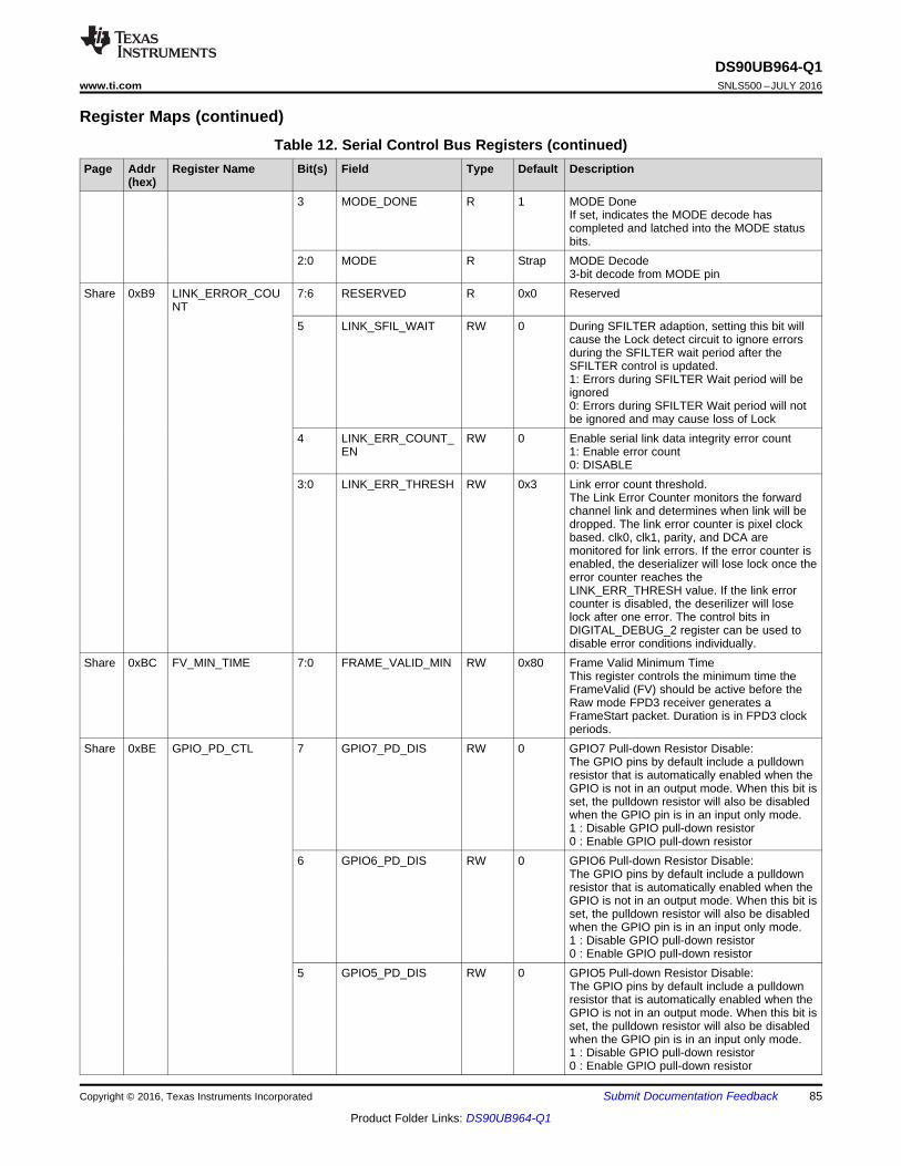
85
DS90UB964-Q1www.ti.com SNLS500 –JULY 2016
Product Folder Links: DS90UB964-Q1
Submit Documentation FeedbackCopyright © 2016, Texas Instruments Incorporated
Register Maps (continued)Table 12. Serial Control Bus Registers (continued)
Page Addr(hex)
Register Name Bit(s) Field Type Default Description
3 MODE_DONE R 1 MODE DoneIf set, indicates the MODE decode hascompleted and latched into the MODE statusbits.
2:0 MODE R Strap MODE Decode3-bit decode from MODE pin
Share 0xB9 LINK_ERROR_COUNT
7:6 RESERVED R 0x0 Reserved
5 LINK_SFIL_WAIT RW 0 During SFILTER adaption, setting this bit willcause the Lock detect circuit to ignore errorsduring the SFILTER wait period after theSFILTER control is updated.1: Errors during SFILTER Wait period will beignored0: Errors during SFILTER Wait period will notbe ignored and may cause loss of Lock
4 LINK_ERR_COUNT_EN
RW 0 Enable serial link data integrity error count1: Enable error count0: DISABLE
3:0 LINK_ERR_THRESH RW 0x3 Link error count threshold.The Link Error Counter monitors the forwardchannel link and determines when link will bedropped. The link error counter is pixel clockbased. clk0, clk1, parity, and DCA aremonitored for link errors. If the error counter isenabled, the deserializer will lose lock once theerror counter reaches theLINK_ERR_THRESH value. If the link errorcounter is disabled, the deserilizer will loselock after one error. The control bits inDIGITAL_DEBUG_2 register can be used todisable error conditions individually.
Share 0xBC FV_MIN_TIME 7:0 FRAME_VALID_MIN RW 0x80 Frame Valid Minimum TimeThis register controls the minimum time theFrameValid (FV) should be active before theRaw mode FPD3 receiver generates aFrameStart packet. Duration is in FPD3 clockperiods.
Share 0xBE GPIO_PD_CTL 7 GPIO7_PD_DIS RW 0 GPIO7 Pull-down Resistor Disable:The GPIO pins by default include a pulldownresistor that is automatically enabled when theGPIO is not in an output mode. When this bit isset, the pulldown resistor will also be disabledwhen the GPIO pin is in an input only mode.1 : Disable GPIO pull-down resistor0 : Enable GPIO pull-down resistor
6 GPIO6_PD_DIS RW 0 GPIO6 Pull-down Resistor Disable:The GPIO pins by default include a pulldownresistor that is automatically enabled when theGPIO is not in an output mode. When this bit isset, the pulldown resistor will also be disabledwhen the GPIO pin is in an input only mode.1 : Disable GPIO pull-down resistor0 : Enable GPIO pull-down resistor
5 GPIO5_PD_DIS RW 0 GPIO5 Pull-down Resistor Disable:The GPIO pins by default include a pulldownresistor that is automatically enabled when theGPIO is not in an output mode. When this bit isset, the pulldown resistor will also be disabledwhen the GPIO pin is in an input only mode.1 : Disable GPIO pull-down resistor0 : Enable GPIO pull-down resistor

86
DS90UB964-Q1SNLS500 –JULY 2016 www.ti.com
Product Folder Links: DS90UB964-Q1
Submit Documentation Feedback Copyright © 2016, Texas Instruments Incorporated
Register Maps (continued)Table 12. Serial Control Bus Registers (continued)
Page Addr(hex)
Register Name Bit(s) Field Type Default Description
4 GPIO4_PD_DIS RW 0 GPIO4 Pull-down Resistor Disable:The GPIO pins by default include a pulldownresistor that is automatically enabled when theGPIO is not in an output mode. When this bit isset, the pulldown resistor will also be disabledwhen the GPIO pin is in an input only mode.1 : Disable GPIO pull-down resistor0 : Enable GPIO pull-down resistor
3 GPIO3_PD_DIS RW 0 GPIO3 Pull-down Resistor Disable:The GPIO pins by default include a pulldownresistor that is automatically enabled when theGPIO is not in an output mode. When this bit isset, the pulldown resistor will also be disabledwhen the GPIO pin is in an input only mode.1 : Disable GPIO pull-down resistor0 : Enable GPIO pull-down resistor
2 GPIO2_PD_DIS RW 0 GPIO2 Pull-down Resistor Disable:The GPIO pins by default include a pulldownresistor that is automatically enabled when theGPIO is not in an output mode. When this bit isset, the pulldown resistor will also be disabledwhen the GPIO pin is in an input only mode.1 : Disable GPIO pull-down resistor0 : Enable GPIO pull-down resistor
1 GPIO1_PD_DIS RW 0 GPIO1 Pull-down Resistor Disable:The GPIO pins by default include a pulldownresistor that is automatically enabled when theGPIO is not in an output mode. When this bit isset, the pulldown resistor will also be disabledwhen the GPIO pin is in an input only mode.1 : Disable GPIO pull-down resistor0 : Enable GPIO pull-down resistor
0 GPIO0_PD_DIS RW 0 GPIO0 Pull-down Resistor Disable:The GPIO pins by default include a pulldownresistor that is automatically enabled when theGPIO is not in an output mode. When this bit isset, the pulldown resistor will also be disabledwhen the GPIO pin is in an input only mode.1 : Disable GPIO pull-down resistor0 : Enable GPIO pull-down resistor
RX 0xD0 PORT_DEBUG 7 RESERVED R 0 Reserved6 RESERVED RW 0 Reserved5 SER_BIST_ACT R 0 Serializer BIST active
This register indicates the Serializer is in BISTmode. If the Deserializer is not in BIST mode,this could indicate an error condition.
4:0 RESERVED RW 0x0 ReservedRX 0xD2 AEQ TEST 7:5 ADAPTIVE_EQ_REL
OCK_TIMERW 0x4 Time to wait for lock before incrementing the
EQ to next setting000 : 164 us001 : 328 us010 : 655 us011 : 1.31 ms100 : 2.62 ms101 : 5.24 ms110 : 10.5ms111 : 21.0 ms

87
DS90UB964-Q1www.ti.com SNLS500 –JULY 2016
Product Folder Links: DS90UB964-Q1
Submit Documentation FeedbackCopyright © 2016, Texas Instruments Incorporated
Register Maps (continued)Table 12. Serial Control Bus Registers (continued)
Page Addr(hex)
Register Name Bit(s) Field Type Default Description
4 AEQ_1ST_LOCK_MODE
RW 0 AEQ First Lock Mode This register bit controlsthe Adaptive Equalizer algorithm operation atinitial Receiver Lock.0 : Initial AEQ lock may occur at any value1 : Initial Receiver lock will restart AEQ at 0,providing a more deterministic initial AEQvalue
3 AEQ_RESTART RW/SC 0 Set high to restart AEQ adaptation from initialvalue. This bit is self clearing. Adaption isrestarted.
2 SET_AEQ_FLOOR RW 0 AEQ adaptation starts from a pre-set floorvalue rather than from zero - good in longcable situations
1:0 RESERVED R 0x0 ReservedRX 0xD3 AEQ_STATUS 7:6 RESERVED R 0x0 Reserved
5:3 EQ_STATUS_1 R 0x0 Adaptive EQ Status 12:0 EQ_STATUS_2 R 0x0 Adaptive EQ Status 2
RX 0xD4 ADAPTIVE EQBYPASS
7:5 EQ STAGE 1SELECT VALUE
RW 0x3 EQ select value [5:3] - Used if adaptive EQ isbypassed.
4 AEQ_LOCK_MODE RW 0 Adaptive Equalizer lock modeWhen set to a 1, Receiver Lock status requiresthe Adaptive Equalizer to complete adaption.When set to a 0, Receiver Lock is based onlyon the Lock circuit itself. AEQ may not havestabilized.
3:1 EQ STAGE 2SELECT VALUE
RW 0x0 EQ select value [2:0] - Used if adaptive EQ isbypassed.
0 ADAPTIVE EQBYPASS
RW 0 1: Disable adaptive EQ0: Enable adaptive EQ
RX 0xD5 AEQ_MIN_MAX 7:4 AEQ_MAX RW 0xF Adaptive Equalizer Maximum valueThis register sets the maximum value for theAdaptive EQ algorithm.
3:0 ADAPTIVE EQFLOOR VALUE
RW 0x8 When AEQ floor is enabled by registerreg_35[5:4] the starting setting is given bythis register.
RX 0xD8 PORT_ICR_HI 7:2 RESERVED R 0x0 Reserved2 IE_FPD3_ENC_ERR RW 0 Interrupt on FPD-Link III Receiver Encoding
ErrorWhen enabled, an interrupt is generated ondetection of an encoding error on the FPD-LinkIII interface for the receive port as reported inthe FPD3_ENC_ERROR bit in theRX_PORT_STS2 register
1 IE_BCC_SEQ_ERR RW 0 Interrupt on BCC SEQ Sequence Error Whenenabled, an interrupt is generated if aSequence Error is detected for the Bi-directional Control Channel forward channelreceiver as reported in the BCC_SEQ_ERRORbit in the RX_PORT_STS1 register.
0 IE_BCC_CRC_ERR RW 0 Interrupt on BCC CRC error detectWhen enabled, an interrupt is generated if aCRC error is detected on a Bi-directionalControl Channel frame received over the FPD-Link III forward channel as reported in theBCC_CRC_ERROR bit in theRX_PORT_STS1 register.
RX 0xD9 PORT_ICR_LO 7 RESERVED RW 0 Reserved

88
DS90UB964-Q1SNLS500 –JULY 2016 www.ti.com
Product Folder Links: DS90UB964-Q1
Submit Documentation Feedback Copyright © 2016, Texas Instruments Incorporated
Register Maps (continued)Table 12. Serial Control Bus Registers (continued)
Page Addr(hex)
Register Name Bit(s) Field Type Default Description
6 IE_LINE_LEN_CHG RW 0 Interrupt on Video Line lengthWhen enabled, an interrupt is generated if thelength of the video line changes. Status isreported in the LINE_LEN_CHG bit in theRX_PORT_STS2 register.
5 IE_LINE_CNT_CHG RW 0 Interrupt on Video Line countWhen enabled, an interrupt is generated if thenumber of video lines per frame changes.Status is reported in the LINE_CNT_CHG bit inthe RX_PORT_STS2 register.
4 IE_BUFFER_ERR RW 0 Interrupt on Receiver Buffer ErrorWhen enabled, an interrupt is generated if theReceive Buffer overflow is detected asreported in the BUFFER_ERROR bit in theRX_PORT_STS2 register.
3 RESERVED RW 0 Reserved2 IE_FPD3_PAR_ERR RW 0 Interrupt on FPD-Link III Receiver Parity Error
When enabled, an interrupt is generated ondetection of parity errors on the FPD-Link IIIinterface for the receive port. Parity error statusis reported in the PARITY_ERROR bit in theRX_PORT_STS1 register.
1 IE_PORT_PASS RW 0 Interrupt on change in Port PASS statusWhen enabled, an interrupt is generated on achange in receiver port valid status as reportedin the PORT_PASS bit in the PORT_STS1register.
0 IE_LOCK_STS RW 0 Interrupt on change in Lock StatusWhen enabled, an interrupt is generated on achange in lock status. Status is reported in theLOCK_STS_CHG bit in the RX_PORT_STS1register.
RX 0xDA PORT_ISR_HI 7:3 Reserved R 0x0 Reserved2 IS_FPD3_ENC_ERR R 0 FPD-Link III Receiver Encode Error Interrupt
StatusAn encoding error on the FPD-Link III interfacefor the receive port has been detected. Statusis reported in the FPD3_ENC_ERROR bit inthe RX_PORT_STS2 register.This interrupt condition is cleared by readingthe RX_PORT_STS2 register.
1 IS_BCC_SEQ_ERR R 0 BCC CRC Sequence Error Interrupt StatusA Sequence Error has been detected for theBi-directional Control Channel forward channelreceiver. Status is reported in theBCC_SEQ_ERROR bit in theRX_PORT_STS1 register.This interrupt condition is cleared by readingthe RX_PORT_STS1 register.
0 IS_BCC_CRC_ERR R 0 BCC CRC error detect Interrupt StatusA CRC error has been detected on a Bi-directional Control Channel frame receivedover the FPD-Link III forward channel. Statusis reported in the BCC_CRC_ERROR bit in theRX_PORT_STS1 register.This interrupt condition is cleared by readingthe RX_PORT_STS1 register.
RX 0xDB PORT_ISR_LO 7 RESERVED R 0 Reserved

89
DS90UB964-Q1www.ti.com SNLS500 –JULY 2016
Product Folder Links: DS90UB964-Q1
Submit Documentation FeedbackCopyright © 2016, Texas Instruments Incorporated
Register Maps (continued)Table 12. Serial Control Bus Registers (continued)
Page Addr(hex)
Register Name Bit(s) Field Type Default Description
6 IS_LINE_LEN_CHG R 0 Video Line Length Interrupt StatusA change in video line length has beendetected. Status is reported in theLINE_LEN_CHG bit in the RX_PORT_STS2register.This interrupt condition is cleared by readingthe RX_PORT_STS2 register.
5 IS_LINE_CNT_CHG R 0 Video Line Count Interrupt StatusA change in number of video lines per framehas been detected. Status is reported in theLINE_CNT_CHG bit in the RX_PORT_STS2register.This interrupt condition is cleared by readingthe RX_PORT_STS2 register.
4 IS_BUFFER_ERR R 0 Receiver Buffer Error Interrupt StatusA Receive Buffer overflow has been detectedas reported in the BUFFER_ERROR bit in theRX_PORT_STS2 register.This interruptcondition is cleared by reading theRX_PORT_STS2 register.
3 RESERVED R 0 Reserved2 IS_FPD3_PAR_ERR R 0 FPD-Link III Receiver Parity Error Interrupt
StatusA parity error on the FPD-Link III interface forthe receive port has been detected. Parity errorstatus is reported in the PARITY_ERROR bit inthe RX_PORT_STS1 register.This interrupt condition is cleared by readingthe RX_PORT_STS1 register.
1 IS_PORT_PASS R 0 Port Valid Interrupt StatusA change in receiver port valid status asreported in the PORT_PASS bit in thePORT_STS1 register. This interrupt conditionis cleared by reading the RX_PORT_STS1register.
0 IS_LOCK_STS R 0 Lock Interrupt StatusA change in lock status has been detected.Status is reported in the LOCK_STS_CHG bitin the RX_PORT_STS1 register.This interrupt condition is cleared by readingthe RX_PORT_STS1 register.
Share 0xF0 FPD3_RX_ID0 7:0 FPD3_RX_ID0 R 0x5F FPD3_RX_ID0: First byte ID code: ‘_’Share 0xF1 FPD3_RX_ID1 7:0 FPD3_RX_ID1 R 0x55 FPD3_RX_ID1: 2nd byte of ID code: ‘U’Share 0xF2 FPD3_RX_ID2 7:0 FPD3_RX_ID2 R 0x42 FPD3_RX_ID2: 3rd byte of ID code: ‘B’Share 0xF3 FPD3_RX_ID3 7:0 FPD3_RX_ID3 R 0x39 FPD3_RX_ID3: 4th byte of ID code: ‘9’Share 0xF4 FPD3_RX_ID4 7:0 FPD3_RX_ID4 R 0x36 FPD3_RX_ID4: 5th byte of ID code: '6'Share 0xF5 FPD3_RX_ID5 7:0 FPD3_RX_ID5 R 0x34 FPD3_RX_ID5: 6th byte of ID code: '4'Share 0xF8 I2C_RX0_ID 7:1 RX_PORT0_ID RW 0x0 7-bit Receive Port 0 I2C ID
Configures the decoder for detectingtransactions designated for Receiver port 0registers. This provides a simpler method ofaccessing device registers specifically for port0 without having to use the paging function toselect the register page. A value of 0 in thisfield disables the Port0 decoder.
0 RESERVED R 0 Reserved

90
DS90UB964-Q1SNLS500 –JULY 2016 www.ti.com
Product Folder Links: DS90UB964-Q1
Submit Documentation Feedback Copyright © 2016, Texas Instruments Incorporated
Register Maps (continued)Table 12. Serial Control Bus Registers (continued)
Page Addr(hex)
Register Name Bit(s) Field Type Default Description
Share 0xF9 I2C_RX1_ID 7:1 RX_PORT1_ID RW 0x0 7-bit Receive Port 1 I2C IDConfigures the decoder for detectingtransactions designated for Receiver port 1registers. This provides a simpler method ofaccessing device registers specifically for port1 without having to use the paging function toselect the register page. A value of 0 in thisfield disables the Port1 decoder.
0 RESERVED R 0 ReservedShare 0xFA I2C_RX2_ID 7:1 RX_PORT2_ID RW 0x0 7-bit Receive Port 2 I2C ID
Configures the decoder for detectingtransactions designated for Receiver port 2registers. This provides a simpler method ofaccessing device registers specifically for port2 without having to use the paging function toselect the register page. A value of 0 in thisfield disables the Port2 decoder.
0 RESERVED R 0 ReservedShare 0xFB I2C_RX3_ID 7:1 RX_PORT3_ID RW 0x0 7-bit Receive Port 3 I2C ID
Configures the decoder for detectingtransactions designated for Receiver port 3registers. This provides a simpler method ofaccessing device registers specifically for port3 without having to use the paging function toselect the register page. A value of 0 in thisfield disables the Port3 decoder.
0 RESERVED R 0 Reserved

91
DS90UB964-Q1www.ti.com SNLS500 –JULY 2016
Product Folder Links: DS90UB964-Q1
Submit Documentation FeedbackCopyright © 2016, Texas Instruments Incorporated
8.7.1 Indirect Access RegistersSeveral functional blocks include register sets contained in the Indirect Access map (Table 13); i.e. PatternGenerator, CSI-2 timing, and Analog controls. Register access is provided via an indirect access mechanismthrough the Indirect Access registers (IND_ACC_CTL, IND_ACC_ADDR, and IND_ACC_DATA). These registersare located at offsets 0xB0-0xB2 in the main register space.
The indirect address mechanism involves setting the control register to select the desired block, setting theregister offset address, and reading or writing the data register. In addition, an auto-increment function isprovided in the control register to automatically increment the offset address following each read or write of thedata register.
For writes, the process is as follows:1. Write to the IND_ACC_CTL register to select the desired register block2. Write to the IND_ACC_ADDR register to set the register offset3. Write the data value to the IND_ACC_DATA register
If auto-increment is set in the IND_ACC_CTL register, repeating step 3 will write additional data bytes tosubsequent register offset locations
For reads, the process is as follows:1. Write to the IND_ACC_CTL register to select the desired register block2. Write to the IND_ACC_ADDR register to set the register offset3. Read from the IND_ACC_DATA register
If auto-increment is set in the IND_ACC_CTL register, repeating step 3 will read additional data bytes fromsubsequent register offset locations.
Table 13. Indirect Register Map DescriptionIA Select0xB0[5:2] Page/Block Indirect Registers Address Range Description
0000 0 Digital Page 0 Indirect Registers0x01-0x1F Pattern Gen Registers0x40-0x51 CSI TX port 0 Timing Registers0x60-0x71 CSI TX port 1 Timing Registers
0001 1 FPD3 Channel 0 Reserved Registers 0x00-0x14 Reserved0010 2 FPD3 Channel 1 Reserved Registers 0x00-0x14 Reserved0011 3 FPD3 Channel 2 Reserved Registers 0x00-0x14 Reserved0100 4 FPD3 Channel 3 Reserved Registers 0x00-0x14 Reserved0101 5 FPD3 Share Reserved Registers 0x00-0x04 Reserved0110 6 Write All FPD3 Reserved Registers 0x00-0x14 Reserved0111 7 CSI TX Reserved Registers 0x00-0x1D Reserved

92
DS90UB964-Q1SNLS500 –JULY 2016 www.ti.com
Product Folder Links: DS90UB964-Q1
Submit Documentation Feedback Copyright © 2016, Texas Instruments Incorporated
Table 14. Digital Page 0 Indirect RegistersIndirectPage
Addr(hex)
Register Name Bit(s) Field Type Default Description
Block 0 0x00 Reserved 7:0 RESERVED R 0x0 Reserved0x01 PGEN_CTL 7:1 RESERVED RW 0x0 Reserved
0 PGEN_ENABLE RW 0 Pattern Generator Enable1: Enable Pattern Generator0: Disable Pattern Generator
0x02 PGEN_CFG 7 PGEN_FIXED_EN RW 0 Fixed Pattern EnableSetting this bit enables Fixed Color Patterns.0 : Send Color Bar Pattern1 : Send Fixed Color Pattern
6 RESERVED RW 0 Reserved5:4 NUM_CBARS RW 0x3 Number of Color Bars
00 : 1 Color Bar01 : 2 Color Bars10 : 4 Color Bars11 : 8 Color Bars
3:0 BLOCK_SIZE RW 0x3 Block SizeFor Fixed Color Patterns, this field controlsthe size of the fixed color field in bytes.Allowed values are 1 to 15.
0x03 PGEN_CSI_DI 7:6 PGEN_CSI_VC RW 0x0 CSI Virtual Channel IdentifierThis field controls the value sent in the CSIpacket for the Virtual Channel Identifier
5:0 PGEN_CSI_DT RW 0x24 CSI Data TypeThis field controls the value sent in the CSIpacket for the Data Type. The default value(0x24) indicates RGB888.
0x04 PGEN_LINE_SIZE1 7:0 PGEN_LINE_SIZE[15:8]
RW 0x07 Most significant byte of the Pattern Generatorline size. This is the active line length inbytes. Default setting is for 1920 bytes for a640 pixel line width.
0x05 PGEN_LINE_SIZE0 7:0 PGEN_LINE_SIZE[7:0]
RW 0x80 Least significant byte of the PatternGenerator line size. This is the active linelength in bytes. Default setting is for 1920bytes for a 640 pixel line width.
0x06 PGEN_BAR_SIZE1 7:0 PGEN_BAR_SIZE[15:8]
RW 0x0 Most significant byte of the Pattern Generatorcolor bar size. This is the active length inbytes for the color bars. This value is used forall except the last color bar. The last color baris determined by the remaining bytes asdefined by the PGEN_LINE_SIZE value.
0x07 PGEN_BAR_SIZE0 7:0 PGEN_BAR_SIZE[7:0]
RW 0xF0 Least significant byte of the PatternGenerator color bar size. This is the activelength in bytes for the color bars. This valueis used for all except the last color bar. Thelast color bar is determined by the remainingbytes as defined by the PGEN_LINE_SIZEvalue.
0x08 PGEN_ACT_LPF1 7:0 PGEN_ACT_LPF[15:8]
RW 0x01 Active Lines Per FrameMost significant byte of the number of activelines per frame. Default setting is for 480active lines per frame.
0x09 PGEN_ACT_LPF0 7:0 PGEN_ACT_LPF[7:0] RW 0xE0 Active Lines Per FrameLeast significant byte of the number of activelines per frame. Default setting is for 480active lines per frame.
0x0A PGEN_TOT_LPF1 7:0 PGEN_TOT_LPF[15:8]
RW 0x02 Total Lines Per FrameMost significant byte of the number of totallines per frame including vertical blanking
0x0B PGEN_TOT_LPF0 7:0 PGEN_TOT_LPF[7:0] RW 0x0D Total Lines Per FrameLeast significant byte of the number of totallines per frame including vertical blanking

93
DS90UB964-Q1www.ti.com SNLS500 –JULY 2016
Product Folder Links: DS90UB964-Q1
Submit Documentation FeedbackCopyright © 2016, Texas Instruments Incorporated
Table 14. Digital Page 0 Indirect Registers (continued)IndirectPage
Addr(hex)
Register Name Bit(s) Field Type Default Description
0x0C PGEN_LINE_PD1 7:0 PGEN_LINE_PD[15:8]
RW 0x0C Line PeriodMost significant byte of the line period in 10nsunits. The default setting for the line periodregisters sets a line period of 31.75microseconds.
0x0D PGEN_LINE_PD0 7:0 PGEN_LINE_PD[7:0] RW 0x67 Line PeriodLeast significant byte of the line period in10ns units. The default setting for the lineperiod registers sets a line period of 31.75microseconds.
0x0E PGEN_VBP 7:0 PGEN_VBP RW 0x21 Vertical Back PorchThis value provides the vertical back porchportion of the vertical blanking interval. Thisvalue provides the number of blank linesbetween the FrameStart packet and the firstvideo data packet.
0x0F PGEN_VFP 7:0 PGEN_VFP RW 0x0A Vertical Front PorchThis value provides the vertical front porchportion of the vertical blanking interval. Thisvalue provides the number of blank linesbetween the last video line and theFrameEnd packet.
0x10 PGEN_COLOR0 7:0 PGEN_COLOR0 RW 0xAA Pattern Generator Color 0For Reference Color Bar Patterns, thisregister controls the byte data value sentduring color bar 0.For Fixed Color Patterns,this register controls the first byte of the fixedcolor pattern.
0x11 PGEN_COLOR1 7:0 PGEN_COLOR1 RW 0x33 Pattern Generator Color 1For Reference Color Bar Patterns, thisregister controls the byte data value sentduring color bar 1.For Fixed Color Patterns,this register controls the second byte of thefixed color pattern.
0x12 PGEN_COLOR2 7:0 PGEN_COLOR2 RW 0xF0 Pattern Generator Color 2For Reference Color Bar Patterns, thisregister controls the byte data value sentduring color bar 2.For Fixed Color Patterns,this register controls the third byte of the fixedcolor pattern.
0x13 PGEN_COLOR3 7:0 PGEN_COLOR3 RW 0x7F Pattern Generator Color 3For Reference Color Bar Patterns, thisregister controls the byte data value sentduring color bar 3.For Fixed Color Patterns,this register controls the fourth byte of thefixed color pattern.
0x14 PGEN_COLOR4 7:0 PGEN_COLOR4 RW 0x55 Pattern Generator Color 4For Reference Color Bar Patterns, thisregister controls the byte data value sentduring color bar 4.For Fixed Color Patterns,this register controls the fifth byte of the fixedcolor pattern.
0x15 PGEN_COLOR5 7:0 PGEN_COLOR5 RW 0xCC Pattern Generator Color 5For Reference Color Bar Patterns, thisregister controls the byte data value sentduring color bar 5.For Fixed Color Patterns,this register controls the sixth byte of thefixed color pattern.
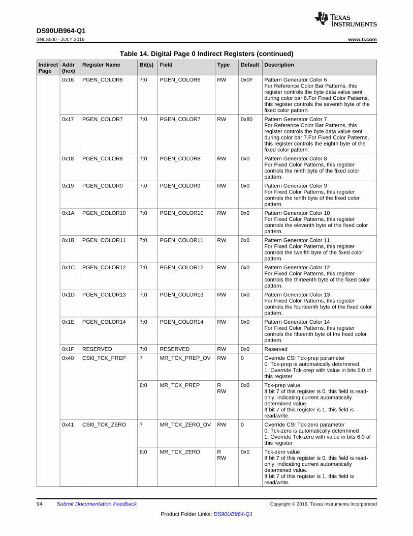
94
DS90UB964-Q1SNLS500 –JULY 2016 www.ti.com
Product Folder Links: DS90UB964-Q1
Submit Documentation Feedback Copyright © 2016, Texas Instruments Incorporated
Table 14. Digital Page 0 Indirect Registers (continued)IndirectPage
Addr(hex)
Register Name Bit(s) Field Type Default Description
0x16 PGEN_COLOR6 7:0 PGEN_COLOR6 RW 0x0F Pattern Generator Color 6For Reference Color Bar Patterns, thisregister controls the byte data value sentduring color bar 6.For Fixed Color Patterns,this register controls the seventh byte of thefixed color pattern.
0x17 PGEN_COLOR7 7:0 PGEN_COLOR7 RW 0x80 Pattern Generator Color 7For Reference Color Bar Patterns, thisregister controls the byte data value sentduring color bar 7.For Fixed Color Patterns,this register controls the eighth byte of thefixed color pattern.
0x18 PGEN_COLOR8 7:0 PGEN_COLOR8 RW 0x0 Pattern Generator Color 8For Fixed Color Patterns, this registercontrols the ninth byte of the fixed colorpattern.
0x19 PGEN_COLOR9 7:0 PGEN_COLOR9 RW 0x0 Pattern Generator Color 9For Fixed Color Patterns, this registercontrols the tenth byte of the fixed colorpattern.
0x1A PGEN_COLOR10 7:0 PGEN_COLOR10 RW 0x0 Pattern Generator Color 10For Fixed Color Patterns, this registercontrols the eleventh byte of the fixed colorpattern.
0x1B PGEN_COLOR11 7:0 PGEN_COLOR11 RW 0x0 Pattern Generator Color 11For Fixed Color Patterns, this registercontrols the twelfth byte of the fixed colorpattern.
0x1C PGEN_COLOR12 7:0 PGEN_COLOR12 RW 0x0 Pattern Generator Color 12For Fixed Color Patterns, this registercontrols the thirteenth byte of the fixed colorpattern.
0x1D PGEN_COLOR13 7:0 PGEN_COLOR13 RW 0x0 Pattern Generator Color 13For Fixed Color Patterns, this registercontrols the fourteenth byte of the fixed colorpattern.
0x1E PGEN_COLOR14 7:0 PGEN_COLOR14 RW 0x0 Pattern Generator Color 14For Fixed Color Patterns, this registercontrols the fifteenth byte of the fixed colorpattern.
0x1F RESERVED 7:0 RESERVED RW 0x0 Reserved0x40 CSI0_TCK_PREP 7 MR_TCK_PREP_OV RW 0 Override CSI Tck-prep parameter
0: Tck-prep is automatically determined1: Override Tck-prep with value in bits 6:0 ofthis register
6:0 MR_TCK_PREP RRW
0x0 Tck-prep valueIf bit 7 of this register is 0, this field is read-only, indicating current automaticallydetermined value.If bit 7 of this register is 1, this field isread/write.
0x41 CSI0_TCK_ZERO 7 MR_TCK_ZERO_OV RW 0 Override CSI Tck-zero parameter0: Tck-zero is automatically determined1: Override Tck-zero with value in bits 6:0 ofthis register
6:0 MR_TCK_ZERO RRW
0x0 Tck-zero valueIf bit 7 of this register is 0, this field is read-only, indicating current automaticallydetermined value.If bit 7 of this register is 1, this field isread/write.

95
DS90UB964-Q1www.ti.com SNLS500 –JULY 2016
Product Folder Links: DS90UB964-Q1
Submit Documentation FeedbackCopyright © 2016, Texas Instruments Incorporated
Table 14. Digital Page 0 Indirect Registers (continued)IndirectPage
Addr(hex)
Register Name Bit(s) Field Type Default Description
0x42 CSI0_TCK_TRAIL 7 MR_TCK_TRAIL_OV RW 0 Override CSI Tck-trail parameter0: Tck-trail is automatically determined1: Override Tck-trail with value in bits 6:0 ofthis register
6:0 MR_TCK_TRAIL RRW
0x0 Tck-trail valueIf bit 7 of this register is 0, this field is read-only, indicating current automaticallydetermined value.If bit 7 of this register is 1, this field isread/write.
0x43 CSI0_TCK_POST 7 MR_TCK_POST_OV RW 0 Override CSI Tck-post parameter0: Tck-post is automatically determined1: Override Tck-post with value in bits 6:0 ofthis register
6:0 MR_TCK_POST RRW
0x0 Tck-post valueIf bit 7 of this register is 0, this field is read-only, indicating current automaticallydetermined value.If bit 7 of this register is 1, this field isread/write.
0x44 CSI0_THS_PREP 7 MR_THS_PREP_OV RW 0 Override CSI Ths-prep parameter0: Ths-prep is automatically determined1: Override Ths-prep with value in bits 6:0 ofthis register
6:0 MR_THS_PREP RRW
0x0 Ths-prep valueIf bit 7 of this register is 0, this field is read-only, indicating current automaticallydetermined value.If bit 7 of this register is 1, this field isread/write.
0x45 CSI0_THS_ZERO 7 MR_THS_ZERO_OV RW 0 Override CSI Ths-zero parameter0: Ths-zero is automatically determined1: Override Ths-zero with value in bits 6:0 ofthis register
6:0 MR_THS_ZERO RRW
0x0 Ths-zero valueIf bit 7 of this register is 0, this field is read-only, indicating current automaticallydetermined value.If bit 7 of this register is 1, this field isread/write.
0x46 CSI0_THS_TRAIL 7 MR_THS_TRAIL_OV RW 0 Override CSI Ths-trail parameter0: Ths-trail is automatically determined1: Override Ths-trail with value in bits 6:0 ofthis register
6:0 MR_THS_TRAIL RRW
0x0 Ths-trail valueIf bit 7 of this register is 0, this field is read-only, indicating current automaticallydetermined value.If bit 7 of this register is 1, this field isread/write.
0x47 CSI0_THS_EXIT 7 MR_THS_EXIT_OV RW 0 Override CSI Ths-exit parameter0: Ths-exit is automatically determined1: Override Ths-exit with value in bits 6:0 ofthis register
6:0 MR_THS_EXIT RRW
0x0 Ths-exit valueIf bit 7 of this register is 0, this field is read-only, indicating current automaticallydetermined value.If bit 7 of this register is 1, this field isread/write.

96
DS90UB964-Q1SNLS500 –JULY 2016 www.ti.com
Product Folder Links: DS90UB964-Q1
Submit Documentation Feedback Copyright © 2016, Texas Instruments Incorporated
Table 14. Digital Page 0 Indirect Registers (continued)IndirectPage
Addr(hex)
Register Name Bit(s) Field Type Default Description
0x48 CSI0_TPLX 7 MR_TPLX_OV RW 0 Override CSI Tplx parameter0: Tplx is automatically determined1: Override Tplx with value in bits 6:0 of thisregister
6:0 MR_TPLX RRW
0x0 Tplx valueIf bit 7 of this register is 0, this field is read-only, indicating current automaticallydetermined value.If bit 7 of this register is 1, this field isread/write.
0x60 CSI1_TCK_PREP 7 MR_TCK_PREP_OV RW 0 Override CSI Tck-prep parameter0: Tck-prep is automatically determined1: Override Tck-prep with value in bits 6:0 ofthis register
6:0 MR_TCK_PREP RRW
0x0 Tck-prep valueIf bit 7 of this register is 0, this field is read-only, indicating current automaticallydetermined value.If bit 7 of this register is 1, this field isread/write.
0x61 CSI1_TCK_ZERO 7 MR_TCK_ZERO_OV RW 0 Override CSI Tck-zero parameter0: Tck-zero is automatically determined1: Override Tck-zero with value in bits 6:0 ofthis register
6:0 MR_TCK_ZERO RRW
0x0 Tck-zero valueIf bit 7 of this register is 0, this field is read-only, indicating current automaticallydetermined value.If bit 7 of this register is 1, this field isread/write.
0x62 CSI1_TCK_TRAIL 7 MR_TCK_TRAIL_OV RW 0 Override CSI Tck-trail parameter0: Tck-trail is automatically determined1: Override Tck-trail with value in bits 6:0 ofthis register
6:0 MR_TCK_TRAIL RRW
0x0 Tck-trail valueIf bit 7 of this register is 0, this field is read-only, indicating current automaticallydetermined value.If bit 7 of this register is 1, this field isread/write.
0x63 CSI1_TCK_POST 7 MR_TCK_POST_OV RW 0 Override CSI Tck-post parameter0: Tck-post is automatically determined1: Override Tck-post with value in bits 6:0 ofthis register
6:0 MR_TCK_POST RRW
0x0 Tck-post valueIf bit 7 of this register is 0, this field is read-only, indicating current automaticallydetermined value.If bit 7 of this register is 1, this field isread/write.
0x64 CSI1_THS_PREP 7 MR_THS_PREP_OV RW 0 Override CSI Ths-prep parameter0: Ths-prep is automatically determined1: Override Ths-prep with value in bits 6:0 ofthis register
6:0 MR_THS_PREP RRW
0x0 Ths-prep valueIf bit 7 of this register is 0, this field is read-only, indicating current automaticallydetermined value.If bit 7 of this register is 1, this field isread/write.

97
DS90UB964-Q1www.ti.com SNLS500 –JULY 2016
Product Folder Links: DS90UB964-Q1
Submit Documentation FeedbackCopyright © 2016, Texas Instruments Incorporated
Table 14. Digital Page 0 Indirect Registers (continued)IndirectPage
Addr(hex)
Register Name Bit(s) Field Type Default Description
0x65 CSI1_THS_ZERO 7 MR_THS_ZERO_OV RW 0 Override CSI Ths-zero parameter0: Ths-zero is automatically determined1: Override Ths-zero with value in bits 6:0 ofthis register
6:0 MR_THS_ZERO RRW
0x0 Ths-zero valueIf bit 7 of this register is 0, this field is read-only, indicating current automaticallydetermined value.If bit 7 of this register is 1, this field isread/write.
0x66 CSI1_THS_TRAIL 7 MR_THS_TRAIL_OV RW 0 Override CSI Ths-trail parameter0: Ths-trail is automatically determined1: Override Ths-trail with value in bits 6:0 ofthis register
6:0 MR_THS_TRAIL RRW
0x0 Ths-trail valueIf bit 7 of this register is 0, this field is read-only, indicating current automaticallydetermined value.If bit 7 of this register is 1, this field isread/write.
0x67 CSI1_THS_EXIT 7 MR_THS_EXIT_OV RW 0 Override CSI Ths-exit parameter0: Ths-exit is automatically determined1: Override Ths-exit with value in bits 6:0 ofthis register
6:0 MR_THS_EXIT RRW
0x0 Ths-exit valueIf bit 7 of this register is 0, this field is read-only, indicating current automaticallydetermined value.If bit 7 of this register is 1, this field isread/write.
0x68 CSI1_TPLX 7 MR_TPLX_OV RW 0 Override CSI Tplx parameter0: Tplx is automatically determined1: Override Tplx with value in bits 6:0 of thisregister
6:0 MR_TPLX RRW
0x0 Tplx valueIf bit 7 of this register is 0, this field is read-only, indicating current automaticallydetermined value.If bit 7 of this register is 1, this field isread/write.
LEGEND:• RW = Read Write• RW/SC = RW/SC = Read Write access/Self Clearing bit• R/P = Read Only, Permanent value• R/COR = Read Only, Clear On Read

98
DS90UB964-Q1SNLS500 –JULY 2016 www.ti.com
Product Folder Links: DS90UB964-Q1
Submit Documentation Feedback Copyright © 2016, Texas Instruments Incorporated
9 Application and Implementation
NOTEInformation in the following applications sections is not part of the TI componentspecification, and TI does not warrant its accuracy or completeness. TI’s customers areresponsible for determining suitability of components for their purposes. Customers shouldvalidate and test their design implementation to confirm system functionality.
9.1 Application InformationThe DS90UB964-Q1 is a highly integrated camera hub chip which includes four FPD-Link III inputs targeted atADAS applications, such as front/rear/surround-view cameras, camera monitoring systems, and sensor fusion.
9.1.1 Power Over CoaxSee application report Sending Power over Coax in DS90UB913A Designs for more details.

VDD_FPD1
VDD_FPD2
VDDL1
VDDL2
VDD_CSI0
VDD18_P0
VDD18_P1
CSI0_CLKN
CSI0_CLKP
CSI0_D0N
CSI0_D0P
CSI0_D1N
CSI0_D1P
CSI0_D2N
GPIO[0]
GPIO[1]
GPIO[2]
GPIO[3]
GPIO[4]
GPIO[5]
PDB
VDD_CSI1
DAP
1.8V1.1V
1.8V
CSI-2 Outputs
GPIO[7:0]
FB1 FB4
10k
0.01µF
t 0.1µF
RIN0+
RIN0-
RIN1+
RIN1-MODE
IDx
I2C_SDA
I2C_SCL
VDDIO
I2C
C1
C2
C3
C4
R1
R2R3
R4
4.7k 4.7k
NOTE:FB1-FB9: DCR<=25mQ; Z=120Q@100MHzC1,C3,C5,C7 = 100nF (50 WV; 0402) with DS90UB913AC2,C4,C6,C8 = 47nF (50 WV; 0402) with DS90UB913AR1 and R2 (see IDx Resistor Values Table)R3 and R4 (see MODE Resistor Values Table)RTERM = 50QRT = 100
1µF 0.1µF 1µF0.1µF
GPIO[6]
CSI0_D2P
IN_D2NCSI0_D3N
CSI0_D3P
CSI1_CLKN
CSI1_CLKP
CSI1_D0N
CSI1_D0P
CSI1_D1N
CSI1_D1P
CSI1_D2N
CSI1_D2P
IN_D2NCSI1_D3N
CSI1_D3P
FB2 1µF 0.1µF
FB3 1µF 0.1µF
INTB
TESTEN
Control
Status
CMLOUTP
CMLOUTN
HUB Deserializer
1.8V
>10µF
0.1µF
0.1µF
0.01µF
t 0.1µF
0.01µF
t 0.1µF
0.01µF
t 0.1µF
0.01µF
t 0.1µF
0.01µF
t 0.1µF
0.01µF
t 0.1µF
0.01µF
t 0.1µF
FPD-Link IIIRTERM
RTERM
RIN2+
RIN2-
RIN3+
RIN3-
C5
C6
C7
C8
RTERM
RTERM
VDDIO(Filtered)
4.7k
GPIO[7]
I2C_SDA2
I2C_SCL2
4.7k 4.7k
REFCLK25 MHz
(100ppm)
0.01µF
t 0.1µF
0.01µF
t 0.1µF
VDD18_P2
VDD18_P3
1µF 0.1µF
VDDIO0.01µF
t 0.1µF
VDDIO
VDD18_FPD0
VDD18_FPD1
FB81µF0.1µF 10µF0.01µF
t 0.1µF
0.01µF
t 0.1µF
0.01µF
t 0.1µF
0.01µF
t 0.1µF
VDD18_FPD2
VDD18_FPD3
VDD18A 1.8VFB91µF0.1µF
0.01µF
t 0.1µF
(TEST_PAD)
Control10k
RT
99
DS90UB964-Q1www.ti.com SNLS500 –JULY 2016
Product Folder Links: DS90UB964-Q1
Submit Documentation FeedbackCopyright © 2016, Texas Instruments Incorporated
9.2 Typical Application
Figure 38. Typical Connection Diagram (Coaxial)

DOUT-
DOUT+
SER
RIN-
RIN+
DES
50Q 50Q
DOUT-
DOUT+
SER
RIN-
RIN+
DES
100
DS90UB964-Q1SNLS500 –JULY 2016 www.ti.com
Product Folder Links: DS90UB964-Q1
Submit Documentation Feedback Copyright © 2016, Texas Instruments Incorporated
Typical Application (continued)9.2.1 Design RequirementsFor the typical design application, use use the parameters listed in Table 15.
Table 15. Design ParametersDESIGN PARAMETER EXAMPLE VALUE
VDDIO 1.8 V or 3.3 VVDD11 1.1 VVDD18 1.8 V
AC Coupling Capacitor for STP with 913AQ/913Q/933Q: RIN[3:0]± 100 nF (50 WV 0402)AC Coupling Capacitor for Coaxial with 913AQ/933Q: RIN[3:0]+ 100 nF (50 WV 0402)AC Coupling Capacitor for Coaxial with 913AQ/933Q: RIN[3:0]- 47 nF (50 WV 0402)
The SER/DES supports only AC-coupled interconnects through an integrated DC-balanced decoding scheme.External AC-coupling capacitors must be placed in series in the FPD-Link III signal path as shown in Figure 39.For applications utilizing single-ended 50-Ω coaxial cable, terminate the unused data pins (RIN0–, RIN1–, RIN2–,RIN3–) with an AC-coupling capacitor and a 50-Ω resistor.
Figure 39. AC-Coupled Connection (STP)
Figure 40. AC-Coupled Connection (Coaxial)
For high-speed FPD–Link III transmissions, use the smallest available package for the AC-coupling capacitor tohelp minimize degradation of signal quality due to package parasitics.
9.2.2 Detailed Design ProcedureFigure 44 and Figure 44 show typical applications of the DS90UB964-Q1 for multi-camera surround view system.From Figure 38, the FPD-Link III must have an external 0.100 μF / 0.47 μF AC coupling capacitors for coaxialinterconnects. The same AC coupling capacitor values should be matched on the paired serializer boards. Thedeserializer has an internal termination. Bypass capacitors are placed near the power supply pins. At a minimum,0.1μF or 0.01μF capacitors should be used for each of the core supply pins for local device bypassing. Ferritebeads are placed on the VDD18 and VDD11 supplies for effective noise suppression.

HUBDeserializer
DS90UB913ASerializer
DS90UB913ASerializer
DS90UB913ASerializer
DS90UB913ASerializer
CS
I-2
TX
P
ort 0
RAW10/12
RAW10/12
RAW10/12
RAW10/12
MIPI CSI-21.6 Gbps/lane X 4 Host / ISP
CS
I-2
Out
put (
500
mV
/DIV
)
Time (50 ns/DIV)
CS
I-2
Out
put (
500
mV
/DIV
)
Time (50 ns/DIV)
101
DS90UB964-Q1www.ti.com SNLS500 –JULY 2016
Product Folder Links: DS90UB964-Q1
Submit Documentation FeedbackCopyright © 2016, Texas Instruments Incorporated
9.2.3 Application Curves
Figure 41. CSI-2 DATA and CLK Output Figure 42. CSI-2 DATA and Continuous CLK Output
9.3 System Examples
Figure 43. Four DS90UB913A Camera Data onto CSI-2 over 1 port

HUBDeserializer
DS90UB913ASerializer
DS90UB913ASerializer
DS90UB913ASerializer
DS90UB913ASerializer
CS
I-2
TX
P
ort 0
CS
I-2
TX
P
ort 1
RAW10/12
MIPI CSI-21.6 Gbps/lane X 4
RAW10/12
RAW10/12
RAW10/12
Host / ISP
MIPI CSI-21.6 Gbps/lane X 4 Host / ISP
102
DS90UB964-Q1SNLS500 –JULY 2016 www.ti.com
Product Folder Links: DS90UB964-Q1
Submit Documentation Feedback Copyright © 2016, Texas Instruments Incorporated
System Examples (continued)
Figure 44. Four DS90UB913A Camera Data onto CSI-2 over 2 ports

VDD11
REFCLK
T1
VDD18
VDDIO
T3
PDBHard Reset
T2
T6 T7T5
T4
T0
103
DS90UB964-Q1www.ti.com SNLS500 –JULY 2016
Product Folder Links: DS90UB964-Q1
Submit Documentation FeedbackCopyright © 2016, Texas Instruments Incorporated
10 Power Supply RecommendationsThis device provides separate power and ground pins for different portions of the circuit. This is done to isolateswitching noise effects between different sections of the circuit. Separate planes on the PCB are typically notrequired. Table 1 provides guidance on which circuit blocks are connected to which power pin pairs. In somecases, an external filter many be used to provide clean power to sensitive circuits such as PLLs.
10.1 VDD Power SupplyEach VDD power supply pin must have a 10 nF (or 100 nF) capacitor to ground connected as close as possibleto DS90UB964-Q1 device. TI recommends having additional decoupling capacitors (0.1 µF, 1 µF, and 10 µF) oni and also recommends having the pins connected to a solid power plane.
10.2 Power-Up SequencingThe power-up sequence for the DS90UB964-Q1 is as follows:
Table 16. Timing Diagram for the Power-Up SequencePARAMETER MIN TYP MAX UNIT NOTES
T0 VDD11 to VDD18 to VDDIO 0 msT1 VDD11 rise time 0.05 ms @10/90%T2 VDD11 to VDD18 0 msT3 VDD18 rise time 0.2 1 ms @10/90%T4 VDD18 to VDDIO 0 msT5 VDDIO rise time 0.2 1 ms @10/90%T6 VDDIO to PDB 0 msT7 PDB pulse width 2 ms Hard reset
Figure 45. Power-Up Sequencing
10.3 PDB PinThe PDB pin is active HIGH and must remain LOW while the VDD pin power supplies are in transition. Anexternal RC network on the PDB pin may be connected to ensure PDB arrives after all the supply pins havesettled to the recommended operating voltage. When PDB pin is pulled up to VDD18, a 10-kΩ pullup and a > 10-μF capacitor to GND are required to delay the PDB input signal rise. All inputs must not be driven until bothpower supplies have reached steady state.

104
DS90UB964-Q1SNLS500 –JULY 2016 www.ti.com
Product Folder Links: DS90UB964-Q1
Submit Documentation Feedback Copyright © 2016, Texas Instruments Incorporated
PDB Pin (continued)Table 17. PDB Pin Pulse Width
PARAMETER TEST CONDITIONS MIN TYP MAX UNITPDBtLRST PDB Reset Low Pulse 2 ms
10.4 GroundTI recommends that only one board ground plane be used in the design. This provides the best image plane forsignal traces running above the plane. Connect the thermal pad of the DS90UB964-Q1 to this plane with vias.

105
DS90UB964-Q1www.ti.com SNLS500 –JULY 2016
Product Folder Links: DS90UB964-Q1
Submit Documentation FeedbackCopyright © 2016, Texas Instruments Incorporated
11 Layout
11.1 Layout GuidelinesCircuit board layout and stack-up for the FPD-Link III devices must be designed to provide low-noise power feedto the device. Good layout practice also separates high frequency or high-level inputs and outputs to minimizeunwanted stray noise pickup, feedback, and interference. Power system performance may be greatly improvedby using thin dielectrics (2 to 4 mils) for power/ground sandwiches. This arrangement provides plane capacitancefor the PCB power system with low-inductance parasitics, which has proven especially effective at highfrequencies, and makes the value and placement of external bypass capacitors less critical. External bypasscapacitors should include both RF ceramic and tantalum electrolytic types. RF capacitors may use values in therange of 0.01 µF to 0.1 µF. Ceramic capacitors may be in the 2.2-µF to 10-µF range. The voltage rating of theceramic capacitors must be at least 5× the power supply voltage being used
TI recommends surface-mount capacitorsdue to their smaller parasitics. When using multiple capacitors persupply pin, locate the smaller value closer to the pin. A large bulk capacitor is recommend at the point of powerentry. This is typically in the 50-µF to 100-µF range, which smooths low frequency switching noise. TIrecommends connectingpower and ground pins directly to the power and ground planes with bypass capacitorsconnected to the plane with via on both ends of the capacitor. Connecting power or ground pins to an externalbypass capacitor increases the inductance of the path.
A small body size X7R chip capacitor, such as 0603 or 0402, is recommended for external bypass. Its small bodysize reduces the parasitic inductance of the capacitor. The user must pay attention to the resonance frequency ofthese external bypass capacitors, usually in the range of 20 to 30 MHz. To provide effective bypassing, multiplecapacitors are often used to achieve low impedance between the supply rails over the frequency of interest. Athigh frequency, it is also a common practice to use two vias from power and ground pins to the planes, reducingthe impedance at high frequency.
Some devices provide separate power and ground pins for different portions of the circuit. This is done to isolateswitching noise effects between different sections of the circuit. Separate planes on the PCB are typically notrequired. Pin Description tables typically provide guidance on which circuit blocks are connected to which powerpin pairs. In some cases, an external filter may be used to provide clean power to sensitive circuits such as PLLs
Use at least a four-layer board with a power and ground plane. Locate LVCMOS signals away from thedifferential lines to prevent coupling from the LVCMOS lines to the differential lines. Differential impedance of 100Ω are typically recommended for STP interconnect and single-ended impedance of 50 Ω for coaxial interconnect.The closely coupled lines help to ensure that coupled noise appears as common-mode and thus is rejected bythe receivers. The tightly coupled lines aso radiate less.
11.1.1 CSI-2 Guidelines1. Route CSI0_D*P/N and CSI1_D*P/N pairs with controlled 100-Ω differential impedance (±20%) or 50-Ω
single-ended impedance (±15%).2. Keep away from other high-speed signals.3. Keep length difference between a differential pair to 5 mils of each other.4. Length matching should be near the location of mismatch.5. Match trace lengths between pairs to be < 25 mils.6. Each pair should be separated at least by 3 times the signal trace width.7. Keep the use of bends in differential traces to a minimum. When bends are used, the number of left and right
bends must be as equal as possible, and the angle of the bend should be ≥ 135 degrees. This arrangementminimizes any length mismatch caused by the bends and therefore minimizes the impact that bends have onEMI.
8. Route all differential pairs on the same layer.9. Keep the number of VIAS to a minimum — TI recommends keeping the VIA count to 2 or fewer.10. Keep traces on layers adjacent to ground plane.11. Do NOT route differential pairs over any plane split.12. Adding Test points causes impedance discontinuity and therefore negatively impacts signal performance. If
test points are used, place them in series and symmetrically. Test points must not be placed in a manner thatcauses a stub on the differential pair.

PR
OC
ES
SO
R
pin
1
CSI0_CLKP/N
CSI0_D0P/N
CSI0_D1P/N
CSI0_D2P/N
CSI0_D3P/NRIN0+/-
RIN1+/-
RIN3+/-
RIN2+/-
106
DS90UB964-Q1SNLS500 –JULY 2016 www.ti.com
Product Folder Links: DS90UB964-Q1
Submit Documentation Feedback Copyright © 2016, Texas Instruments Incorporated
11.2 Layout ExampleStencil parameters such as aperture area ratio and the fabrication process have a significant impact on pastedeposition. Inspection of the stencil prior to placement of the VQFN package is highly recommended to improveboard assembly yields. If the via and aperture openings are not carefully monitored, the solder may flowunevenly through the DAP.
Example PCB layout is used to demonstrate both proper routing and proper solder techniques when designing inthe Deserializer.
Figure 46. Simplified Layout Example
Figure 47 shows a PCB layout example are derived from the layout design of the DS90UB96X-Q1EVMEvaluation Board. The graphic and layout description are used to determine proper routing when designing theboard. The high speed FPD-Link III traces routed differentially up to the connector. A 100Ω differentialcharacteristic impedance and 50Ω single-ended characteristic impedance traces are maintained as much aspossible for both STP and coaxial applications. For the layout of a coaxial interconnects, coupled traces shouldbe used with the RINx- termination near to the connector.
Figure 47. DS90UB964-Q1 Example PCB Layout

107
DS90UB964-Q1www.ti.com SNLS500 –JULY 2016
Product Folder Links: DS90UB964-Q1
Submit Documentation FeedbackCopyright © 2016, Texas Instruments Incorporated
Layout Example (continued)

108
DS90UB964-Q1SNLS500 –JULY 2016 www.ti.com
Product Folder Links: DS90UB964-Q1
Submit Documentation Feedback Copyright © 2016, Texas Instruments Incorporated
12 Device and Documentation Support
12.1 Documentation Support
12.1.1 Related DocumentationFor related documentation see the following:• Sending Power over Coax in DS90UB913A Designs• I2C over DS90UB913/4 FPD-Link III with Bidirectional Control Channel• I2C Communication Over FPD-Link III with Bidirectional Control Channel• I2C Bus Pull-Up Resistor Calculation
12.2 Receiving Notification of Documentation UpdatesTo receive notification of documentation updates, navigate to the device product folder on ti.com. In the upperright corner, click on Alert me to register and receive a weekly digest of any product information that haschanged. For change details, review the revision history included in any revised document.
12.3 Community ResourcesThe following links connect to TI community resources. Linked contents are provided "AS IS" by the respectivecontributors. They do not constitute TI specifications and do not necessarily reflect TI's views; see TI's Terms ofUse.
TI E2E™ Online Community TI's Engineer-to-Engineer (E2E) Community. Created to foster collaborationamong engineers. At e2e.ti.com, you can ask questions, share knowledge, explore ideas and helpsolve problems with fellow engineers.
Design Support TI's Design Support Quickly find helpful E2E forums along with design support tools andcontact information for technical support.
12.4 TrademarksE2E is a trademark of Texas Instruments.All other trademarks are the property of their respective owners.
12.5 Electrostatic Discharge CautionThis integrated circuit can be damaged by ESD. Texas Instruments recommends that all integrated circuits be handled withappropriate precautions. Failure to observe proper handling and installation procedures can cause damage.
ESD damage can range from subtle performance degradation to complete device failure. Precision integrated circuits may be moresusceptible to damage because very small parametric changes could cause the device not to meet its published specifications.
12.6 GlossarySLYZ022 — TI Glossary.
This glossary lists and explains terms, acronyms, and definitions.

PACKAGE OPTION ADDENDUM
www.ti.com 7-Aug-2016
Addendum-Page 1
PACKAGING INFORMATION
Orderable Device Status(1)
Package Type PackageDrawing
Pins PackageQty
Eco Plan(2)
Lead/Ball Finish(6)
MSL Peak Temp(3)
Op Temp (°C) Device Marking(4/5)
Samples
DS90UB964TRGCRQ1 ACTIVE VQFN RGC 64 2000 Green (RoHS& no Sb/Br)
CU NIPDAU Level-3-260C-168 HR -40 to 105 UB964Q
DS90UB964TRGCTQ1 ACTIVE VQFN RGC 64 250 Green (RoHS& no Sb/Br)
CU NIPDAU Level-3-260C-168 HR -40 to 105 UB964Q
(1) The marketing status values are defined as follows:ACTIVE: Product device recommended for new designs.LIFEBUY: TI has announced that the device will be discontinued, and a lifetime-buy period is in effect.NRND: Not recommended for new designs. Device is in production to support existing customers, but TI does not recommend using this part in a new design.PREVIEW: Device has been announced but is not in production. Samples may or may not be available.OBSOLETE: TI has discontinued the production of the device.
(2) Eco Plan - The planned eco-friendly classification: Pb-Free (RoHS), Pb-Free (RoHS Exempt), or Green (RoHS & no Sb/Br) - please check http://www.ti.com/productcontent for the latest availabilityinformation and additional product content details.TBD: The Pb-Free/Green conversion plan has not been defined.Pb-Free (RoHS): TI's terms "Lead-Free" or "Pb-Free" mean semiconductor products that are compatible with the current RoHS requirements for all 6 substances, including the requirement thatlead not exceed 0.1% by weight in homogeneous materials. Where designed to be soldered at high temperatures, TI Pb-Free products are suitable for use in specified lead-free processes.Pb-Free (RoHS Exempt): This component has a RoHS exemption for either 1) lead-based flip-chip solder bumps used between the die and package, or 2) lead-based die adhesive used betweenthe die and leadframe. The component is otherwise considered Pb-Free (RoHS compatible) as defined above.Green (RoHS & no Sb/Br): TI defines "Green" to mean Pb-Free (RoHS compatible), and free of Bromine (Br) and Antimony (Sb) based flame retardants (Br or Sb do not exceed 0.1% by weightin homogeneous material)
(3) MSL, Peak Temp. - The Moisture Sensitivity Level rating according to the JEDEC industry standard classifications, and peak solder temperature.
(4) There may be additional marking, which relates to the logo, the lot trace code information, or the environmental category on the device.
(5) Multiple Device Markings will be inside parentheses. Only one Device Marking contained in parentheses and separated by a "~" will appear on a device. If a line is indented then it is a continuationof the previous line and the two combined represent the entire Device Marking for that device.
(6) Lead/Ball Finish - Orderable Devices may have multiple material finish options. Finish options are separated by a vertical ruled line. Lead/Ball Finish values may wrap to two lines if the finishvalue exceeds the maximum column width.
Important Information and Disclaimer:The information provided on this page represents TI's knowledge and belief as of the date that it is provided. TI bases its knowledge and belief on informationprovided by third parties, and makes no representation or warranty as to the accuracy of such information. Efforts are underway to better integrate information from third parties. TI has taken andcontinues to take reasonable steps to provide representative and accurate information but may not have conducted destructive testing or chemical analysis on incoming materials and chemicals.TI and TI suppliers consider certain information to be proprietary, and thus CAS numbers and other limited information may not be available for release.

PACKAGE OPTION ADDENDUM
www.ti.com 7-Aug-2016
Addendum-Page 2
In no event shall TI's liability arising out of such information exceed the total purchase price of the TI part(s) at issue in this document sold by TI to Customer on an annual basis.

TAPE AND REEL INFORMATION
*All dimensions are nominal
Device PackageType
PackageDrawing
Pins SPQ ReelDiameter
(mm)
ReelWidth
W1 (mm)
A0(mm)
B0(mm)
K0(mm)
P1(mm)
W(mm)
Pin1Quadrant
DS90UB964TRGCRQ1 VQFN RGC 64 2000 330.0 16.4 9.3 9.3 1.5 12.0 16.0 Q1
DS90UB964TRGCTQ1 VQFN RGC 64 250 178.0 16.4 9.3 9.3 1.5 12.0 16.0 Q1
PACKAGE MATERIALS INFORMATION
www.ti.com 6-Oct-2016
Pack Materials-Page 1

*All dimensions are nominal
Device Package Type Package Drawing Pins SPQ Length (mm) Width (mm) Height (mm)
DS90UB964TRGCRQ1 VQFN RGC 64 2000 367.0 367.0 38.0
DS90UB964TRGCTQ1 VQFN RGC 64 250 210.0 185.0 35.0
PACKAGE MATERIALS INFORMATION
www.ti.com 6-Oct-2016
Pack Materials-Page 2


IMPORTANT NOTICE
Texas Instruments Incorporated and its subsidiaries (TI) reserve the right to make corrections, enhancements, improvements and otherchanges to its semiconductor products and services per JESD46, latest issue, and to discontinue any product or service per JESD48, latestissue. Buyers should obtain the latest relevant information before placing orders and should verify that such information is current andcomplete. All semiconductor products (also referred to herein as “components”) are sold subject to TI’s terms and conditions of salesupplied at the time of order acknowledgment.TI warrants performance of its components to the specifications applicable at the time of sale, in accordance with the warranty in TI’s termsand conditions of sale of semiconductor products. Testing and other quality control techniques are used to the extent TI deems necessaryto support this warranty. Except where mandated by applicable law, testing of all parameters of each component is not necessarilyperformed.TI assumes no liability for applications assistance or the design of Buyers’ products. Buyers are responsible for their products andapplications using TI components. To minimize the risks associated with Buyers’ products and applications, Buyers should provideadequate design and operating safeguards.TI does not warrant or represent that any license, either express or implied, is granted under any patent right, copyright, mask work right, orother intellectual property right relating to any combination, machine, or process in which TI components or services are used. Informationpublished by TI regarding third-party products or services does not constitute a license to use such products or services or a warranty orendorsement thereof. Use of such information may require a license from a third party under the patents or other intellectual property of thethird party, or a license from TI under the patents or other intellectual property of TI.Reproduction of significant portions of TI information in TI data books or data sheets is permissible only if reproduction is without alterationand is accompanied by all associated warranties, conditions, limitations, and notices. TI is not responsible or liable for such altereddocumentation. Information of third parties may be subject to additional restrictions.Resale of TI components or services with statements different from or beyond the parameters stated by TI for that component or servicevoids all express and any implied warranties for the associated TI component or service and is an unfair and deceptive business practice.TI is not responsible or liable for any such statements.Buyer acknowledges and agrees that it is solely responsible for compliance with all legal, regulatory and safety-related requirementsconcerning its products, and any use of TI components in its applications, notwithstanding any applications-related information or supportthat may be provided by TI. Buyer represents and agrees that it has all the necessary expertise to create and implement safeguards whichanticipate dangerous consequences of failures, monitor failures and their consequences, lessen the likelihood of failures that might causeharm and take appropriate remedial actions. Buyer will fully indemnify TI and its representatives against any damages arising out of the useof any TI components in safety-critical applications.In some cases, TI components may be promoted specifically to facilitate safety-related applications. With such components, TI’s goal is tohelp enable customers to design and create their own end-product solutions that meet applicable functional safety standards andrequirements. Nonetheless, such components are subject to these terms.No TI components are authorized for use in FDA Class III (or similar life-critical medical equipment) unless authorized officers of the partieshave executed a special agreement specifically governing such use.Only those TI components which TI has specifically designated as military grade or “enhanced plastic” are designed and intended for use inmilitary/aerospace applications or environments. Buyer acknowledges and agrees that any military or aerospace use of TI componentswhich have not been so designated is solely at the Buyer's risk, and that Buyer is solely responsible for compliance with all legal andregulatory requirements in connection with such use.TI has specifically designated certain components as meeting ISO/TS16949 requirements, mainly for automotive use. In any case of use ofnon-designated products, TI will not be responsible for any failure to meet ISO/TS16949.
Products ApplicationsAudio www.ti.com/audio Automotive and Transportation www.ti.com/automotiveAmplifiers amplifier.ti.com Communications and Telecom www.ti.com/communicationsData Converters dataconverter.ti.com Computers and Peripherals www.ti.com/computersDLP® Products www.dlp.com Consumer Electronics www.ti.com/consumer-appsDSP dsp.ti.com Energy and Lighting www.ti.com/energyClocks and Timers www.ti.com/clocks Industrial www.ti.com/industrialInterface interface.ti.com Medical www.ti.com/medicalLogic logic.ti.com Security www.ti.com/securityPower Mgmt power.ti.com Space, Avionics and Defense www.ti.com/space-avionics-defenseMicrocontrollers microcontroller.ti.com Video and Imaging www.ti.com/videoRFID www.ti-rfid.comOMAP Applications Processors www.ti.com/omap TI E2E Community e2e.ti.comWireless Connectivity www.ti.com/wirelessconnectivity
Mailing Address: Texas Instruments, Post Office Box 655303, Dallas, Texas 75265Copyright © 2016, Texas Instruments Incorporated