Dr.-Ing. Artur Seibt - w140.comw140.com/Handbook_of_Oscilloscope_Technology.pdf · Dr.-Ing. Artur...
418
Dr.-Ing. Artur Seibt Handbook of Oscilloscope Technology Circuitry – Accessories - Measurement – Selection Criteria - Service 2 nd extended and updated edition 2006
Transcript of Dr.-Ing. Artur Seibt - w140.comw140.com/Handbook_of_Oscilloscope_Technology.pdf · Dr.-Ing. Artur...

Dr.-Ing. Artur Seibt Handbook of Oscilloscope Technology Circuitry – Accessories - Measurement – Selection Criteria - Service 2nd extended and updated edition 2006

2
Preface to the second edition 2005. After ten years from its first edition this handbook needed updating. HAMEG Instruments
GmbH, a major manufacturer of both Combiscopes and analog scopes,
a subsidiary of Rohde & Schwarz, sponsored this second edition. Repetitions are intentional,
because this book is also intended for use as a reference to specific topics.
The chapters about basics, analog circuitry, calibration, service and repair hints required only
minor changes and additions; they remain important as there is a multitude of analog scopes
in use, also many measurement tasks can not be fulfilled with any scope out of current
production (e.g. 10 uV/cm). As there were few new accessories, the important chapter 10 is
as valid as ever.
Due to the predominance of DSOs meanwhile, the pertinent chapter 6 was considerably
extended.
As socalled Combiscopes were and remain the optimum choice, they were given
extensive treatment in a new chapter 7 with special consideration to the HAMEG 1508.
A greater selection of screen photos further assists the interested reader in his difficult task
of making his choice
Vienna, March 2006.
3
Table of Contents.
1. Oscilloscope families.
1.1 Introduction and principle. 1.2 Integrated and plug-in instruments
2. Oscilloscope displays 2.1 Cathode ray tubes (crt’s) 2.1.1 Electron optics basics
2.1.2 Beam generation and forming
2.1.3 Beam control, unblanking
2.1.4 Electrostatic deflection
2.1.5 Segmented deflection plates
2.1.6 Magnetic deflection
2.1.7 Methods of acceleration
2.1.8 Display distortions
2.1.9 Focus distortions
2.1.10 Types of phosphors
2.1.11 Writing rate
2.1.12 Graticule
2.1.13 Light filters.
2.2 Operation of cathode ray tubes 2.2.1 Generation of high voltage
2.2.2 Generation of auxiliary voltages
2.2.3 Unblanking
2.2.4 External interferences
2.2.5 Handling of crt’s
2.3 Storage cathode ray tubes. 2.3.1 Basics of storage
2.3.2 Bistable storage crt’s
2.3.3 Transmission storage crt’s

4
2.3.4 Transfer storage crt’s
2.3.5 Scan converter crt’s
2.4 Special cathode ray tubes.
2.4.1 Microchannel secondary electron multiplier crt
3. Analog oscilloscopes. 3.1 Block diagram of integrated instruments 3.2 Block diagrams of plug-in instruments. 3.3 Vertical channel. 3.3.1 Requirements
3.3.2 Properties of active components
3.3.3 Basic circuits
3.3.4 Properties of passive components
3.3.5 Input attenuators
3.3.6 Preamplifiers and their operating modes
3.3.7 Trigger signal take-off
3.3.8 Delay lines
3.3.9 Output stages
3.3.10 Adjustment of vertical amplifiers
3.4 Horizontal channel 3.4.1 Block diagram and operating modes
3.4.2 Interface to the vertical channel
3.4.3 Trigger circuits
3.4.4 Sawtooth generators
3.4.5 Horizontal output amplifiers
3.5 Additional features 3.5.1 Calibrators
3.5.2 Readout
3.5.3 t, Delta t, V, Delta V, f etc.
3.5.4 Auxiliary inputs and outputs

5
3.6 Power supplies 3.6.1 Linear regulators
3.6.2 SMPS
3.7 Operation and control 3.7.1 Direct operation
3.7.2 Indirect operation
3.7.3 Remote control
4. Analog storage oscilloscopes 4.1 General remarks 4.2 Bistable storage oscilloscopes 4.3 Transmission storage oscilloscopes 4.4. Transfer storage oscilloscopes 5. Sampling Oscilloscopes. 5.1 History. 5.2 Application of Sampling Oscilloscopes (SO’s) and DSO’s 5.2.1 Common characteristics.
5.2.2 SO’s
5.2.3 DSO’s
5.3 Basics of sampling 5.3.1 Common characteristics of the sampling methods
5.3.2 Real Time Sampling /RTS)
5.3.3 Single Event Sampling
5.3.4 Equivalent Time Sampling (ETS)
5.3.5 Random Sampling (RS)
5.3.6 False displays.
5.4 Vertical Channel 5.4.1 Sampling gate and sampling pulse generation

6
5.4.2 Sampling probes
5.4.3 Sampling gates with termination; „sampling heads“.
5.4.4 Sampling gates with trigger take-off, delay line with termination.
5.4.5 Feed-through samplers, reflectometer.
5.4.6 Hints for troubleshooting and adjustments.
5.4.7 Output stage.
5.5 Horizontal Channel. 5.5.1 Real Time Sampling (RTS)
5.5.2 Special circuits
5.5.3 Equivalent Time Sampling
5.5.4 Random Sampling (RS)
5.5.5 Hints for troubleshooting and adjustments
Kapitel 6, zu überarbeiten und zu ergänzen, folgt Kapitel 7 wird gänzlich neu „Combiscopes“ mit dem Hameg 1508 als zentralem Gegenstand. Die Kapitel 8 .. 12 werden noch überarbeitet und folgen.

7
1. Oscilloscope families.
1.1 Introduction and Principle.
The instruments covered here are called oscillo“scopes“ although they should rather be
called oscillo“graphs“ because they do not „see“ but „write“ waveforms on the screen;
however, this expression is standardized.
Early oscilloscopes were by far no measuring instruments, waveforms could only be
observed qualitatively.
1947 saw the birth of the oscilloscope as we know it today when two engineers (with some
partners who later left) founded Tektronix Inc. in Portland OR, USA. This company presented
the first calibrated oscilloscope, type 511 (10 MHz, 0.25 V/cm, 0.1 us/cm, $ 795, 50 lbs.).
Already this first instrument contained an impressive number of achievements and
innovations in circuitry to be found in every oscilloscope to this date witnessing a profound
understanding of the fundamentals of electronics. The most important innovations were:
- The principle of the enforced operating point:
At that time there were only electron tubes available. Tubes are unequalled for linear low
distortion amplification, especially, as they do not change their characteristics when
driven and because they are immune to temperature. However, they age, also their
characteristics depend on the heater voltage. The amplification of all active elements
depends on the current; if the current is held constant the amplification will remain
constant. This is the prerequisite for a calibrated instrument. Tektronix introduced the
principle of enforced operating current into all stages which influence the calibration
either by using current generators or approximating those by a large resistor returned to
a large voltage.
- Introduction of the difference amplifier.
Making use of the principle of enforced operating current causes the complete loss of
amplification in simple stages. Only by using difference amplifiers is it possible to keep
the operating currents stable while retaining amplification. This is only one reason for its
introduction, far and above the difference amplifier and especially its extended version
as a cascode is the only dc-coupled wide band amplifier worth that designation.
- Regulated power supplies.

8
- Perfect pulse response.
Correct measurement of nonsinusoidal waveforms requires perfect pulse response
- Triggered, calibrated time base.
Former instruments had to be synchronized with the measuring signal in order to obtain
a stable display, hence the time base could not be calibrated.
The value of this new instrument was immediately recognized, the company grew
enormously, its leadership was often challenged but rarely with success, and when only
temporarily. Modern electronics is inconceivable without the modern oscilloscope, it remains
hence its most important measuring instrument. Since then the oscilloscope remained the
domain of American companies markedly proving their superiority in electronics. While later
there appeared some Japanese instruments of partly impressive quality European firms
never played any significant role regarding top performance instruments. The most important
European company, a part of Philips, was sold to Fluke in 93.
There is no room to describe the whole oscilloscope history. 1954 Tektronix introduced the
first plug-in oscilloscope, the series 530. 1957 the 540 series followed (30 MHz), the work
horse of the next decades. Both series used distributed tube amplifiers: input and output
capacitances were built into associated delay lines eliminating them practically. The
bandwidth of the amplifier, however, was not extended to the bandwidth of the delay lines
because these do not exhibit Gaussian behaviour. The amplifications of the individual stages
of a distributed amplifier only add as their currents add up at the output impedance. The
delay line consisted of appr. 30 elements with an equal number of trim capacitors the
alignment of which was more of an art.
1959 the first scope with a higher bandwidth (85 MHz, 0.1 V/cm, 10 ns/cm) appeared, the
581/5, still using distributed tube amplifiers throughout the vertical except for a few
transistors at the input stage and also tubes in the other sections except for a tunnel
diode/transistor trigger circuit. The crt had distributed deflection plates, the delay line was
already a special cable.
The aforementioned instruments although nearly completely equipped with tubes presented
an extraordinarily high standard of quality, not surpassed to date, hardly touched. In order to
reach certain performance levels the tubes in some stages (e.g. horizontal output) had to be
heavily overstressed, causing tubes to fail after some time. So their ability to carry heavy

9
overloads for extended periods of time - in contrast to all semiconductors – gave rise to the
unjustified opinion that tubes were less reliable than semiconductors.
The first fully transistorized (except for input nuvistors) oscilloscope was the type 766 (25
MHz) by Fairchild/Dumont, however, of poor performance.
1962 Tektronix presented their first fully transistorized (except for nuvistors in the vertical,
trigger inputs and the time bases) 647 (50 MHz, 10 mV/cm, 10 ns/cm) oscilloscope with no
compromises in performance, a top product with some specifications never again achieved
to this date like a working temperature spec of – 30 to + 65 degrees C, no fan. 1967 the
enhanced type 647 A with 100 MHz followed. Today’s „modern“ instruments can not match
such temperature specs and need a loud fan. This is called progress.
1969 Tektronix introduced the 7000 series „New Generation“ at the San Francisco
WESCON, setting the standard for the next decades until production ceased in 1992. Since
the production stop many measurement tasks can not be fulfilled any more by any of the
currently available scopes, e.g. 10 uV/cm. However, at the introduction the 150 MHz 7704
was topped by the HP 183 A with 250 MHz which already had ic‘s in the vertical amplifier.
A milestone in scope design was 1972 the 7904 (A) with 500 (600) MHz and a superb (not
the first units) 24 KV crt which allows signals with a rep rate down to 100 Hz still to be seen
at roomlight. This assured Tektronix again the leadership in wide bandwidth scopes.
Companion plug-ins for the 7904 (A) were the dual channel 7 A 24 (450 MHz, 5 mV/cm) and
the single channel 7 A 19 (600 MHz, 10 mV/cm), both with 50 ohm inputs. This type is still
the author’s workhorse.
The 1 GHz 7104 appeared in 1979 and was the highest performance analog scope ever,
using the microchannel secondary emission crt with its extreme writing rate. This instrument,
however, is not destined for everyday universal use due to the limited life of the crt, its
smaller area and its lower intensity. Consequently, the 7104 shuts the crt down
automatically when it was not used for some time. it is deplorable that there never came a
„normal“ 1 GHz scope with a crt like the one in the 7904 A.
The production of a new familiy of analog scopes, the series 11000, was discontinued shortly
after its release towards the end of the 80‘s. The reasons were not technical deficiencies but
the practical impossibility of operating the instruments: the plug-ins had no controls at all, the
mainframe had only one knob, the functions had to be selected by touching the screen.
Touching a screen used to be a criminal offense while Howard Vollum still was president.

10
Apart from Tektronix only HP played any major role with respect to high performance scopes.
When DSOs surfaced LeCroy soon achieved a leading position.
Regarding storage oscilloscopes Tektronix presented the first low-cost bistable instrument in
1963, the 564. Shortly thereafter HP presented the first usable transmission storage scope.
In the 70‘s Tektronix took the lead again with the first transfer storage scope (7834, 7934). In
addition to those there was the Tektronix scan converter.
Today, some try to create the impression as if some important features appeared first in
DSOs. Nothing is further from the truth. Only the storage and display of slow phenomena and
diverse mathematical operations came first with DSOs. HP already had very good 1 GHz
sampling scopes in the beginning 60‘s. Tektronix needed until 1967 to gain the lead with the
first practical random sampling plug-in 3 T 2, the first 3 GHz sampling scope plug-in 4 S 2 A
and the reflectometer plug-in 1 S 2. 1969 the sampling heads (S 1 etc., up to 14 GHz)
followed which were plugged into associated plug-ins (3 S 2, 3 S 5 etc.) but could also be
operated externally. The sampling scopes of that time could be operated also in real time
sampling mode, modulating the sampling repetition frequency in order to break up false
displays.
Also already in 1967 a plug-in pair 3 A 5/3 B 5 (for the 560 series mainframes, 15 MHz) was
in series production which adjusted the vertical sensitivity and the time base speed
automatically to any input signal, it was also completely remotely programmable.
In the same year programmable oscilloscopes and computer-controlled automated
measuring installations were available which performed e.g. the following functions and sent
the information to a computer resp. printed the results: amplitude, rise/fall times, time
differences, frequency, period. These functions were mostly used in conjunction with
sampling plug-ins (3 S 5/ 3 T 5, 3 S 6/ 3 T 6 etc.) and offered performances up to 4 GHz/2
mV/cm in 68 and 14 GHz/2 mV/cm in 69. These specifications should be compared to those
of today’s DSOs not overlooking the fundamental difference of infinite vertical resolution
instead of jittery 8 bits, also, their A/D converters were high resolution high accuracy single or
dual slope converters.
Last not least the complete accessory program was available already in the 60‘s, most
accessories are still in series production today, some only received new names after some
cosmetic touch-ups. Instead of presenting the numbers on the front panel they are now
shown on a display.

11
In the 80‘s DSOs rose to competitors of the analog scopes. Tektronix had already a 7854
analog/digital „Combiscope“ (500 MHz) far earlier. DSOs overtook analog scopes in sales in
the 90‘s because of their much higher prices. The profit is higher with DSOs not only due to
the higher prices, but because their manufacturing cost is also considerably lower. Also,
companies without the intricate knowhow required for analog scopes could now offer DSOs.
DSOs displays operate at very low frequencies because they are all sampling scopes and
the sampling process is nothing else but a frequency down conversion process (see chapter
5). Consequently, cheap mass produced pc monitors are sufficient for display while analog
crt’s are complicated and very expensive. DSOs are nothing else but pc’s with an analog
front end and consist mainly of the same cheap chips. Also, some DSO’s use the same
Microsoft operating software as pc’s. The mathematical functions which come for free since
microcomputers are incorporated anyway are another good reason to ask for higher prices
increasing profits.
While there are massive marketing efforts in favour of DSO’s there is a lack of neutral,
correct, and pertinent technical information for the customer. Even when buying a DSO the
customer receives only an operating manual which just describes which buttons to press but
does not convey any information about how the instrument operates. With most DSOs there
is not even a warning given that false and erroneous displays are possible. To the contrary:
there are DSO manufacturers who ridicule buyers of their former models telling them, while
presenting their newest models, how poor their predecessors were!
Tektronix, Philips/Fluke and Hameg offered/offer Combiscopes which unite the advantages of both worlds and thus are the scopes of first choice.
The laws of physics can not be changed or dispensed with: only analog scopes present the
signal as it is and in real time; a DSO is unable to show the true signal, it can only display a
more or less falsified reconstruction (!) of the signal displayed on a slow time base. This is
such a fundamental difference that every DSO is inferior to a good analog scope – except for
such applications where a true advantage of a DSO is required.
False measurements are impossible with analog scopes, provided its limited rise time is
borne in mind and it is not overdriven. However, in order to obtain reliable, correct
measurements with DSOs the user needs vast specialized knowhow. The user must already
know what the unknown signal looks like in order to recognize false displays.

12
A simple example: when displaying a 1 KHz square wave with extremely short rise and fall
times a DSO will show the slopes and even equally bright, misleading the user to believe that
the slopes were slow. This is a false display as the slopes must not be visible at the slow
time base setting (e.g. 0.5 ms/cm) for the display of 1 KHz. In order to pin down the false
display the user would have to switch the interpolation off (not possible in many DSO’s!). But
the user must first of all suspect the display to be false, why should he else switch the
interpolation off. But even worse: if the unsuspecting user believes the digitally displayed rise
and fall times of the false display he will see figures which are orders of magnitude (!) false.
The purpose of a scope should be to show the user an unknown signal as it truly is, how can
it be expected of the user that he knows the unknown signal better than the instrument?
This book’s purpose is to offer the reader the knowhow enabling him to understand scopes,
to operate them, to judge them correctly and especially to select the right instrument.
Fig. 1.1 shows the principle of an analog scope: an amplifier with variable gain applies the
input signal to the vertical deflection plates of a crt. At the same time the input signal is
routed to a socalled trigger circuit which generates a square wave signal at a point of the
signal which can be selected. This starts the time base which generates a sawtooth i.e. a
voltage which increases linearly with time and applies it to the horizontal deflection plates.
The time base also generates a signal which turns the crt trace on for the duration of the
sweep. The time base scale is defined by the slope of the sawtooth. The scope is completed
by the addition of regulated low voltage power supplies for the amplifier and time base
stages and a regulated high voltage power supply for the crt.
Fig.1.1: Block diagram of an analog scope.
1.2 Integrated and plug-in instruments.
Obviously, it is not possible to realize an amplifier with a bandwidth of 350 MHz and a
sensitivity of 10 uV/cm; even if it existed it would be impossible to create an attenuator
capable of attenuating a signal down to 20 V/cm at 350 MHz. An analog scope and a
sampling scope resp. a DSO can be combined in one instrument (Combiscope), however,
such an instrument must be more expensive than either instrument but will still be less
expensive than both.
Hence very early a basic decision had to be taken: should customers be forced to buy
several specialized instruments or should the manufacturer rather offer adaptable
instruments – comparable to a camera with several lenses.

13
As mentioned one of the founders and president of Tektronix at that time (and a proficient
photographer), Howard Vollum, presented 1954 the first plug-in oscilloscope (530 series)
against heavy internal resistance. Portable (all-in-one) oscilloscopes remained the second
important product line, destined in the first place for service purposes. This first line of plug-in
scopes had the vertical input amplifier in the plug-in as shown in fig. 1.2.
Fig. 1.2: Plug-in oscilloscope with the vertical input amplifier in the plug-in (e.g. Tektronix
series 530, 540, 580).
This was the optimum solution for wide bandwidth oscilloscopes as the expensive and big
vertical output amplifier had to be paid for only once. Already this first plug-in series (marked
by 1 X Y; X = character identifying the type of plug-in: A = amplifier, L = spectrum analyzer, T
= time base, S = sampling vertical, Y = running number) comprised, apart from single and
multichannel vertical amplifiers, sampling and spectrum analyzer plug-ins.
Many applications do not require wide bandwidth, a rather simple and low power output
amplifier will do. Here, it would not make sense to operate an expensive high dissipation
vertical output amplifier in the mainframe. This applies to low frequency applications and all
sampling and spectrum analyzer instruments. Therefore Tektronix created the 560 series as
shown in fig. 1.3: here the two plug-ins contain the complete vertical amplifier resp. the
complete time base, the mainframe contains merely the power supply and the crt. The
mainframe thus was low cost, so it was much easier to buy normal and storage mainframes.
Most plug-ins could be used in the Y or X compartment thus allowing e.g. XY operation of
two amplifiers.
Fig. 1.3: Plug-in oscilloscope with the complete vertical and horizontal circuitry in the plug-ins
(e.g. Tektronix 560 series).
Fig. 1.4 shows a mixed design first used in the Tektronix 647 (A) on which the New
Generation 7000 series was later based: both output amplifiers remain in the mainframe,
there are 2 plug-ins (up to 4 in the 7000 series) which contain the vertical preamplifier resp.
the time base minus its output stage. The plug-in interfaces were identical in all
compartments so any plug-in could be used in any place (apart from special plug-ins).
Fig. 1.4: Plug-in oscilloscope with vertical preamplifier and time base in the plug-ins and the
output stages in the mainframe (e.g. Tektronix 647 (A) and 7000 series).

14
The 7000 series offered a variety of mainframes, normal and several storage types, with
staggered bandwidths up to 1 GHz and a large assortment of vertical amplifier and time base
plug-ins from 10 uV/cm and up to 0.5 ns/cm, in addition sampling, spectrum analyzer, digital
multimeter, counter, curve tracer and special plug-ins. There were also calibrator plug-ins
(067-0587-01/02) for the calibration resp. standardization of the mainframes so that each
plug-in would perform in every mainframe. This was extremely profitable for the customers
as they could buy a maximum of performance and versatility at minimum cost and bench
space needed.
Today, there are no plug-in scopes available out of current production except for some
extremely expensive specialized DSOs. The 7000 series was discontinued in 92 and is only
available second-hand. Unequalled performance and high quality speak for 7000 series
instruments as well as their easy and low cost repair. Some important measuring tasks can
not any more be solved by current scopes, e.g. 10 uV/cm.
2. Oscilloscope displays. 2.1 Cathode ray tubes (crt’s). 2.1.1 Electron optics basics. Apart from rare special cases and some cheap (both meanings of this word intended) DSOs
the majority of oscilloscopes still use cathode ray tubes (crt’s). Beam generation, forming and
control are identical both for electrostatic and magnetic deflection. The fields of application
are defined by the methods of deflection: the deflection plates of an electrostatically deflected
crt constitute pure capacitances (a few pF) while the deflection coils or yokes of magnetically
deflected crt’s are complicated structures unsuitable for higher frequency operation. As long
as the application can live with low frequencies, e.g. a raster display just above the flicker
limit, magnetically deflected crt’s are less expensive, brighter and shorter, also it is easy to
realize large screen displays as known from tv sets. These advantages become more
prevalent as the bandwidth of an oscilloscope increases: laboratory scopes with
electrostatically deflected crt’s attain 1 GHz, special crt’s with a display area of e.g. 12 x 10
mm2 and a length of 400 mm (Philips F) reach 7 GHz. Such crt’s are extremely complicated
and expensive. If a frequency conversion method like sampling or spectrum analysis is used
(all DSO’s are sampling scopes) inexpensive crt’s will do, independent of the bandwidth of
the instrument. This is a major reason why DSO manufacturers aggressively market their
products. However, it should be kept in mind that DSO’s can only offer an inferior signal

15
reproduction due to the sampling process and the additional A/D converter and signal
reconstruction errors.
Fig. 2.1 shows the 5 electron optical areas inside a crt.:
Fig. 2.1: The 5 electron optical areas of a crt.
- Triode: beam generation system, identical to that of any electron tube except for the shape.
- Focus area: Electron optical lenses in this area focus the beam onto the screen.
- Deflection area: Here the deflection plate pairs and their shields of electrostatically
deflected crt’s are located. The deflection coils of magnetically deflected crt’s are normally
placed outside this area, but their fields take effect here.
- Drift or post-acceleration area.
- Screen.
There is so much special literature about electron optics around that it may suffice here to
just present some basics. Pure acceleration of an electron in an electric field is one practical
case, illustrated in picture 2.2 : The electron is traveling in the direction of increasing
potential, its direction is normal to the equipotential lines. It leaves the field without a change
of its direction but at a higher speed dependent on the potential difference seen.
Picture 2.2: Pure acceleration of an electron in an electric field.
The second important case is shown in fig. 2.3: An electron enters a field perpendicular to its
direction with the speed vax. The axial component of its velocity remains unchanged but a
radial component is added, so that the electron leaves the field deflected and accelerated.
Fig. 2.3: Deflection and acceleration of an electron in an electric field.
In the third case shown in fig. 2.4 an electron enters a field at an angle: it will experience a
change in its axial velocity but no change in radial velocity, it is accelerated and deflected in
the direction of the field lines.
Fig. 2.4: Deflection and acceleration of an electron entering a field at an angle.
16
Almost as easily as planar fields curved equipotential planes can be generated, e.g. by grids
bent to shape as shown in fig. 2.5.
Fig. 2.5: Lens created by circularly curved equipotential planes.
The lens thus created may be convergent or divergent. First the case of increasing potential
is studied. If the electron passes through a convex equipotential line it will be bent towards
the axis, the lens is thus convergent. If the electron passes through a concave equipotential
line it will be bent away from the axis, the lens is thus divergent. The size of the angle will
depend on the field strength, the initial electron velocity and the curvature of the lines. If the
initial velocity is increased the angle will decrease, the faster electron is harder to deflect. If
the curvature of the field is increased (smaller circle diameter) the angle will increase, the
lens became stronger. If the field strength is increased the equipotentials lines move closer
together. As long as the electron’s direction remains normal to the equipotential lines there
will be no change of direction, only in velocity.
If the electron travels in the direction of decreasing potential (3rd drawing in picture 2.5) the
effect of the lens will be reversed, the velocity of the electron will decrease, the lens will be
divergent.
2.1.2 Beam generation and forming. Fig. 2.6 depicts the basic construction and field pattern of the triode section. The differences
between this structure and that of an amplifier tube lie only in the mechanical shape. Here a
pencil-shaped beam is desired. The triode consists of the cathode, the grid and the first
anode. The cathode is a nickel cap coated with barium and strontium oxides. It contains a
heater. The grid is a cup with a hole just above the cathode. The first anode is a cylinder with
a small entry hole next to the grid cup and operated several kilovolts above the cathode
potential. The grid is operated as is usual with electron tubes at some negative voltage with
respect to the cathode. The high voltage is necessary in the fist place in order to achieve a
high intensity beam (resp. picture), secondly a thin well focused beam is desired; electrons
are equal polarity charges which repel each other and thus tend to widen the beam.
Fig. 2.6: Field pattern between cathode, grid and first anode.
Fig. 2.6 shows a very much simplified field pattern within the triode. In the center area the
equipotential lines are almost straight. In the area of the anode aperture the lens is concave,

17
thus divergent; in this area the electron velocity is already quite high, therefore the effect of
this lens is weak.
In the area grid – cathode the situation is quite different. Here the equipotential lines are
drawn through the grid aperture towards the cathode, the lens is convex and quite strong
because the velocity is still low. The cathode may be thought of as a multitude of point
sources emitting electrons not only with different speeds due to the spread in thermal energy
but also at different angles, they experience a decrease in radial velocity and an increase in
axial velocity thus bending them towards the axis until they cross it. Due to the differences in
thermal energy and emission angle there is a spread in the point of crossover. At the
crossover the beam has its smallest crossection. The focused spot on the screen is the
image of the crossover so its size determines largely the resulting spot size.
Size and location of the crossover depend upon the triode dimensions and the grid voltage;
as the grid voltage is changed in order to change the intensity the focus will change also,
hence, as a rule, the focus has to be readjusted any time the intensity was changed. In some
scopes this readjustment of the focus is done automatically.
Only 1 .. 10 % of the cathode current reach the screen, most of the current is intercepted by
such electrodes which are positive with respect to the cathode. In order to get typical screen
currents of a few uA cathode currents of mA may be necessary, hence the cathode is quite
heavily stressed. This is further aggravated by the fact that depending on the field pattern
only a small part of the cathode may emit. Therefore it is good practice, in order to extend the
life of expensive crt’s, to set the intensity not higher than necessary and turn the beam
completely off when not used. The cathode life is further dependent on the heater voltage
and its construction. There are robust heaters which, however, require some watts, but last
longer. Portable scopes have crt’s with rather fragile low-wattage heaters with a shorter life.
In older scopes the heaters were powered by the line transformer, the voltage was thus
dependent on the mains voltage; modern scopes have SMPS which generate stabilized
heater voltages.
Fig. 2.6 also shows that the beam is divergent at its entry into the anode 1 cylinder. The lens
consisting of anode 1- focus ring – anode 2 focuses the beam onto the screen. Its field
pattern is shown in fig. 2.7.
Fig. 2.7: Field pattern of the focusing lens.
18
The lens is at first divergent and decelerating, then convergent and accelerating. The
potential of the center electrode is adjusted by the focus control, that of anode 2 by the
astigmatism control. A higher potential at the focus electrode increases the lens power and
thus shortens the distance to the focused plane. If the focus potential is correctly adjusted
the focus plane is the screen.
A deviation of the beam form from the ideal round one is called astigmastism, it causes
uneven focus over the screen area. The deviation from a round spot is caused by the
deflection plates. The average potential of these plates with respect to ground is dictated by
the Y and X output amplifiers and is typically around + 50 .. 150 V. All other crt electrode
potentials must be referred to this average potential. The potential of anode 2 (mostly
connected to anode 1) can be varied by small amounts (some ten volts) around this average
potential so that the spot remains as round as possible over most of the screen. Many users
have difficulty in setting the 3 controls correctly as they do not know how these function. The
right procedure is: first the intensity is set to the brightness desired, then the astigmatism
control is adjusted so that the focus is as uniform over the screen as possible without any
effort for best focus anywhere. At last the focus control is adjusted for best focus.
With plug-in instruments the average potential may depend on the plug-in inserted, if so a
change of plug-in may require a change of focus and astigmatism as well as of amplitude
and time base calibration!
2.1.3 Beam control, unblanking. Like in any other electron tube the beam intensity can be controlled by the grid – cathode
voltage; this control does not require any power, only voltage. As explained before it is the
average plate potential which dictates all other crt potentials. As this is around + 50 .. + 150
V, the cathode has to be connected to the negative terminal of (almost) the full acceleration
voltage, i.e. typically – 1 .. 3 KV. As the grid must be more negative than the cathode by
some – 50 .. 150 V, there rises the problem how to bridge the potential difference of kilovolts
between the unblanking signal from the sweep circuit and the grid. (See ch. 2.2.2). In ch. 3.4
it is explained that the beam is unblanked for the duration of a full sweep, at 5 s/cm that is 50
s; it is impossible to couple a pulse that long to the grid by a capacitor or transformer. Fig.
2.8 shows the grid-cathode characteristic of a popular crt, the Tektronix T 547 used in the
54X oscilloscope family.
Fig. 2.8: Grid – cathode characteristic of the crt Tektronix T 547.

19
One possibility to circumvent the problem is an additional set of deflection plates between
anode 1 and the focus electrode as shown in fig. 2.9. As long as both plates are on the same
potential the beam will not be influenced and is thus visible. If a voltage is applied to one
plate the beam will be deflected so that it hits anode 1 and will be no longer visible.
Picture 2.9: Deflection blanking of the beam.
As this pair of plates has the same potential as the deflection plates (crt reference potential,
appr. + 50 .. 150 V), there is no problem of dc coupling the unblanking pulse. In reality there
are two sets of plates as otherwise the spot would move on the screen during blanking and
unblanking. There are some serious disadvantages to this method: the full cathode current
will be on at all times, also when the screen is dark, this shortens the crt life. The deflected
beam creates some background lighting which will disturb photographs taken with long
shutter settings, e.g. for single event capture. Sofar known this method was only used in
monoaccelerator crt’s in low frequency scopes.
2.1.4 Electrostatic deflection Fig. 2.10 shows the principal design of a pair of deflection plates between focus lens and
screen.
Fig. 2.10: Principal design of a pair of deflection plates.
The deflection sensitivity is:
Sensitivity (V/cm) = (VA x dpp)/(Lps x lp x Vpp), where (2.1)
VA = Acceleration voltage
Vpp = Deflection voltage applied to the plates
Lps = Distance plates – screen
lp = Length of plates
dpp = Distance between plates
Ideally one would prefer a short, bright, high-sensitivity crt with a large screen. Increasing the
length would be the first answer, but this contradicts today’s compact instrument design.
Reducing the anode voltage would increase the sensitivity, but would deteriorate brightness
and focus. Reducing the distance between plates or lengthening them would increase the

20
sensitivity, but the useful screen area would be diminished. The plates may be bent
outwards, but this would also decrease the sensitivity.
If the plates are too close together or if they are too long part of the beam will be intercepted
as the beam is still quite wide in this area, this will cause a decrease in intensity towards the
sides of the screen. There is always some beam interception so that beam current will hit the
plates, this requires a fairly low output impedance of the Y and X amplifiers. This applies also
to all crt electrodes which are positive with respect to the cathode.
In all crt’s the vertical deflection plates are closest to the cathode as they need the highest
sensitivity. The horizontal deflection plates with their consequently lower sensitivity are much
easier to drive because they receive only a sawtooth signal.
Both sets of plates would capacitively couple their signals to the other set, this would cause
signal distortions. Wide band oscilloscope crt’s have shields between the plate sets, two as a
rule. Their potentials have to be adapted to the respective plate potentials by connecting
them to adjustable voltage dividers, otherwise linearity or/and geometry distortions will result;
these adjustments are normally only internally accessible. A readjustment is only required
after a crt was exchanged.
It is important to realize that the deflection plates indeed are ideal lossless capacitances, a
few pF in wide band crt’s. Therefore it is fairly easy to reach wide bandwidths with
appropriate amplifiers. The crt’s do not contribute any parasitic effects, the signal will be truly
displayed exactly as it reached the plates.
2.1.5 Segmented deflection plates. At high frequencies above appr. 100 MHz an effect shows up which is known from other
areas of electronics similar e.g. to the effect of the gap in a magnetic playback head. The
electrons have a certain velocity as given by the potential difference seen when they reach
the vertical plates, hence they need a finite time to travel through the plate field. If this transit
time equals the signal period (or a multiple thereof) the resulting deflection will be zero.
Consequently, the frequency response will begin to roll off far below this critical frequency.
The only methods to counteract this effect would be either to shorten the plates or to
increase the acceleration voltage; both reduce the sensitivity. This problem was solved
decades ago by dividing the plates into segments, the capacitances of the segments were
built into delay lines as known from distributed amplifiers. Crt’s with bandwidths of 1 GHz
were already available in the 50‘s. At this time they had to be driven directly from external

21
voltages as there were no adequate amplifiers available. The useable screen area was
small, scan expansion was not yet developed. Theoretically, the cut-off frequency should rise
to the cut-off frequency of the delay line if the transit time of the electrons would be identical
to the delay time between two taps resp. segment pairs as the electrons would „see“ always
the same signal phase. In reality the bandwidth realized will be much lower than the cut-off
frequency of the delay line because its amplitude and group delay characteristics deviate
from Gaussian behaviour.
It is evident that pulse distortions will arise if the electron transit time and the delay time are
not identical. If e.g. both become equal at some high frequency the sensitivity will at first be
decreased, then it will rise again towards the frequency where both times are equal. Perfect
pulse response requires Gaussian behaviour (see ch. 3.3.1) which shows a monotonously
falling response.
Fig. 2.11 shows the electrical circuit diagram. As usual and explained later the delay line is
only terminated at one side, otherwise the amplifier would have to deliver twice the current.
Fig. 2.11: Electrical circuit diagram of segmented deflection plates built into delay lines.
The coils of the delay lines are built into the crt, 4 terminals are provided. In place of
individual coils and plate segments HP used a helical structure in the 60‘s, its HP 183
reached 250 MHz and surpassed Tektronix at that time.
Today a 100 MHz scope is regarded as standard, hence this deflection structure is important
although there are even 200 MHz scopes without segmented plates thanks to advanced
scan expansion.
The segmented plate structure is explained with the aid of fig. 2.12.
Fig. 2.12: Rise time of a crt with one and two sets of plates.
It is assumed that there are only 5 electrons at any time within the deflection area. E 1 just
left the deflection field and reaches the screen undeflected. E 5 is the first electron which
traversed the full length of the field and thus is maximally (depending on the acceleration
voltage) deflected by the angle alpha. E 4 will be only deflected by ¾ alpha, E 3 by ½ alpha ,
E 2 by ¼ alpha. The transit time is given by lp/ve = tE. If the deflection voltage V is applied as
a step at time to when just E 1 leaves the field, E 5 will reach the screen after tE, the pulse
displayed will thus have a rise time 0 to 100 % of tE. As the rise time is defined as the time

22
from 10 to 90 % the rise time tR = 0.8 tE. We shall encounter this lengthening of a pulse
again when treating the influence of the finite pulse width of a sampling pulse and the rep
rate.
In the second portion of the picture a structure with two sets of plates is depicted. The plate
sets are built into delay lines with a delay time of tE/2. As before a voltage step is applied at
time to when E 1 is just leaving the field while E 5 is just entering it. E 3 is located exactly in
the center and is about to enter the second plate pair. E 1,2,3 remain undeflected as it
requires tE/2 for the step to reach the second plate pair, the 3 electrons will have left it before
this happens. During the time interval to to (to + tE/2) E 4 will be deflected by ¼ alpha. , E 5
by ½ alpha. After that time E 4 and E 5 will have reached the positions 4‘ and 5‘. At this
moment the step will reach the second plate pair. E 4 is again deflected by ¼ alpha and E 5
by ½ alpha. In total E 4 will have been deflected by ½ alpha and E 5 by alpha. The rise time
on the screen will thus be shortened to ½ x 0.8 tE.
The general rule follows that if the plates are divided into n segments and if the electrical
delay between segments is tE/n the rise time will be reduced to tR = 1/n x 0.8 tE.
The delay lines do not present pure capacitances to the output amplifier but loads of their
characteristic impedance Z. However, the amplifier needs load impedances anyway, and, as
a rule, its output capacitances are also built into a delay line or T coil., see ch. 3.3.
2.1.6 Electromagnetic deflection. A first advantage of magnetic deflection is the fact that the two fields do not affect each other.
As described, generally electrons are both accelerated and deflected in electric fields, in
magnetic fields they are only deflected. Therefore it is impossible to realize large deflection
angles with electrostatic deflection, nonlinearity and defocussing set practical limits. Also, it is
impossible to interleave both deflection fields, both deflection plate pairs have to be placed
one behind the other. Interleaving both deflection fields is no problem with magnetic
deflection. Tv tubes prove that 110 degrees deflection with high accuracy is a reality in large
series production. The deflection errors caused by the coils are in general much lower than
those of deflection plates because the fields are larger with respect to the crossectional area
of the beam.
Also for magnetic deflection a deflection coefficient can be derived, expressed in A/cm.
However, it is more difficult to be calculated as the fields of the coils are quite complicated.
With both methods of deflection it is necessary to calculate the integral of the field distribution

23
in axial direction (Z axis) in order to gain a dimensionless factor A, the socalled deflection
factor which depends only on the geometry of the structure. The sensitivity follows from:
Sensitivity (A/cm) = Sqrt (V)/( A x w x L x uo x sqrt (e/2m))
V = acceleration voltage
A = deflection factor
w = number of turns
L = length of field
uo = permeability, 1.26 G x cm/A
The dependence of the sensitivity on the square root of the voltage and the mass is
remarkable; it is hence comparatively easy to achieve bright displays with a magnetically
deflected crt. In addition there are the advantages of a short length and a large screen.
Some reasons why magnetically deflected crt’s are rarely used in oscilloscopes were already
mentioned: the coils constitute very complicated structures of magnetically and capacitively
coupled partial windings which are resonance circuits as well; therefore they can only be
applied reasonably up to a few KHz. The magnitude of the fields to be created dictate the
electrical and mechanical size of the coils und hence their resonance frequencies. Further,
the energy in the deflection area is 1 to 2 orders of magnitude higher than with electrostatic
deflection. The plate pairs in an electrostatically deflected crt can be well shielded against
each other as they are placed one behind the other while a comparatively good decoupling
or shielding of deflection coils is practically impossible.
The overwhelming majority of magnetically deflected crt’s in tv sets or monitors uses a fixed
raster display, the deflection coils are especially designed for this purpose. Also, many DSOs
use such inexpensive monitors. With raster displays high video frequencies are only
encountered in the grid-cathode circuit where they modulate the beam intensity, the
conditions here are similar to those in electrostatically deflected crt’s. Also here the video
output amplifier – grid-cathode – circuit must be designed for perfect pulse response,
otherwise e.g. overshoots etc. will show up at white-black intensity steps. The grid-cathode
circuit, however, does show deviations from a pure capacitive behaviour at high frequencies
like in any other electron tube.
Recently, influences of such magnetic fields on humans are believed, some north European
states issued laws concerning the maximum permissible field strengths outside tv sets and
monitors.

24
2.1.7 Methods of acceleration. 2.1.7.1 Monoaccelerator crt’s.
Fig. 2.13 shows the internal structure of a simple crt; the expression monoaccelerator means
that there is only one stage of acceleration. As a compromise between the conflicting
requirements on brightness, sensitivity, length etc. crt’s were customary which have the
usual 8 x 10 cm2 screen, about 3 KV and sensitivities of 10 to 30 V/cm.
Fig. 2.13: Internal structure of a simple monoaccelerator crt.
Such crt’s are hence only adequate for low frequency scopes; with some still acceptable
investment in the output amplifiers and their power dissipation about 25 MHz were
achievable, with more modern crt’s 50 MHz are possible. Due to the low voltage the
brightness is insufficient to display signals of low rep rate or fast rise times.
2.1.7.2 Post deflection acceleration crt’s.
Early attempts at post deflection acceleration used several conductive coatings between the
deflection area and the screen which were connected to a voltage divider. Such crt’s showed
compression, i.e. reduction of sensitivity, and distortions. A true innovation was the invention
at Tektronix of a resistive spiral on the inside of the crt between the deflection area and the
screen, the beginning of which was connected to the first acceleration voltage and the end of
which was connected to the second acceleration voltage so that the acceleration field
increased linearly from the deflection area to the screen. This still caused compression but
only minor distortions. This invention made wide band scopes a reality. Typical crt’s of that
kind used a first voltage of 1.67 KV and a total voltage of 10 KV, hence the ratio of total
voltage to first acceleration voltage was 6 : 1. The sensitivities were 6 and 30 V/cm, the
useable screen area only 4 x 10 cm2, later 6 x 10 cm2. Due to the high frequency operation
as well as the higher sensitivity these crt’s had deflection plate shields. Fig. 2.14 shows the
internal structure of these crt’s.
Fig. 2.14: Internal structure of a PDA (post-deflection-acceleration) crt with a resistive spiral.
Fig. 2.15 demonstrates how the compression comes about.: the field lines resp. planes are
convex. All rays which hit those planes other than perpendicular are bent inwards. Close to

25
the screen the field lines become concave, however, the velocity of the beam is already so
high that it is hardly influenced.
Fig. 2.15: Explanation of the origin of compression in crt’s with a resistive spiral.
The compression reduces the sensitivity and the useable screen area, but it also reduces the
beam diameter, so that these crt’s excel by an extremely fine trace never again achieved.
The crt’s discussed later sport screen areas of 6 x 10 to 8 x 10 cm2, but due to their thicker
trace the information content is not higher. Crt’s of this structure were used in scopes up to
100 MHz and were the backbone of the first generation of true measuring oscilloscopes.
2.1.7.3 Scan expansion by mesh grids.
The next step in the evolution of crt’s was the introduction of a mesh grid behind the last
deflection plates; this mesh was either formed like a cylinder or a ball surface. Such a grid
prevents as a first advantage that the post acceleration field influences the deflection area.
The potential planes in the post acceleration area are forced to take on the shape of the
mesh. At first such meshes were just used to suppress the compression, thus increasing the
sensitivity and the screen area, however, the focus deteriorated, also the meshes intercepted
up to 50 % of the beam current; consequently these crt’s had to be operated at higher pda
potentials in order to regain the former brightness. A resistive spiral was still applied from the
mesh to about the middle of the remaining distance to the screen, from its end to the screen
a socalled dag coating. Fig. 2.16 shows the field distribution in such a crt.
Fig. 2.16: Field distribution within a crt with a mesh grid.
The logical next step was the intentional use of a mesh to create a divergent lens in order to
increase the deflection angle. Here the complete inner surface of the crt from the mesh to the
screen was dag coated and the coating was connected to the full post acceleration voltage.
This together with the shape of the mesh created the divergent lens desired which yielded
expansions of more than 2. Again sensitivity and screen area were increased and the focus
reduced by the same factor. Also, all nonlinearities and distortions were augmented. This
was accepted as crt’s for portable scopes just had to be short. The higher sensitivity was
also badly needed as it was difficult to generate high deflection voltages at high frequencies.
At that time transistors with high fT’s did not take more than a few ten volts. Fig. 2.17 shows
the field pattern in such a crt.
Fig. 2.17: Field pattern within a crt with scan expansion mesh .

26
2.1.7.4 Scan expansion using lenses.
The first crt which came to the author’s knowledge using scan expansion with an electron
optical lens was by Telefunken, Ulm, used in a Siemens 100 MHz scope that the author
received for test in 1967. Thomson-CSF developed crt’s with quadrupole and slot lenses
from 1967 on, according to their literature. The advantages are evident: the removal of the
mesh did away with its beam current interception, its distortions and secondary emission
resulting in brighter, sharper and larger displays.
Fig. 2.18 depicts the respective gains in crt length for the 4 types of crt’s mentioned.
Fig. 2.18: Comparison of crt lengths resulting from the use of the 4 methods described.
(Tektronix).
The best crt to the author’s knowledge is the one used in the Philips 200 MHz combiscope
which is also used in all Hameg 100 .. 200 MHz scopes. It operates at 14 KV, uses scan
expansion with lenses and magnets placed in strategic positions inside the tube the
strengths of which are changed during the manufacturing resp. test procedures with the
result of an exceptionally uniform well focused trace, high intensity and linearity.
2.1.8 Display distortions. 2.1.8.1 Tangent error.
The beam can be thought of as originating from the middle of the deflection area; when
deflected its end point will paint the surface of a ball. The screens of all crt’s are planar,
though. Consequently, the focus is decreased form the screen center to its edges, secondly,
for equal amounts of deflection angle the distances covered on the screen will increase
towards the edges, this is a nonlinearity, an expansion. Fig. 2.19 shows this.
Fig. 2.19: Nonlinearity and loss of focus by the tangent error.
2.1.8.2 Geometry distortions.
Stray fields between the deflection plates and their shields resp. the dag coating cause
pincushion or barrel distortions. Depending on the specific crt design the shields or/and the

27
dag coating in this area are connected to an adjustable voltage divider which is adjusted for
minimum distortions of vertical and horizontal lines at the screen edges.
A further reason for geometry distortions are deflection plates without the necessary
corrections. With plates not corrected the length of the beam depends on the deflection
angle. Therefore the plates must be shaped at the beam entrance and exit sides so that the
beam length becomes independent of the angle as shown in Fig. 2.20.
Fig. 2.20: Geometry distortions. Uncorrected plates (left) and corrected plates (right).
2.1.9 Focus distortions. 2.1.9.1 Space charge repulsion.
Electrons repel each other as they are charges of the same polarity. The amount of trace
width increase depends on the number and density of electrons in the beam and their speed.
The inner electrons of the beam repel the outer electrons and thus expand the beam. The
effect is worst in monoaccelerator crt’s because from the deflection area to the screen (drift
region) the electrons travel at the same low speed with a high density. Hence the spot size
on the screen is large due to space charge repulsion. In a pda crt the electrons are strongly
accelerated behind the deflection area so the expansion is less.
Higher intensity decreases the focus as it increases the space charge density and thus
repulsion. A change in grid-cathode bias also changes the location of the crossover which is
focused onto the screen, so a change in intensity always requires a focus readjustment. At
very high beam intensities the effect of repulsion becomes so strong that focusing is no
longer possible.
In order to achieve a reasonable focus still at high beam intensities there is no other solution
but to increase the post acceleration voltage to e.g. 24 KV. At such voltages X ray generation
is to be expected which requires special glass for the crt front.
2.1.9.2 Deflection defocusing.
This is the main reason why it is practically impossible to realize large deflection angles with
electrostatically deflected crt’s. The electric field between a pair of deflection plates not only
deflects the electrons but it also accelerates resp. decelerates them. That plate which is
more positive than the last electrode preceding it will accelerate those electrons passing

28
nearby, the other plate will decelerate those passing by that one. This causes changes in the
velocities and transit times with the effect that the spot on the screen will be elongated in the
direction of the deflection plate field. As the astigmatism causes similar spot deformations the
user must try to achieve best uniform focus with the focus and astigmatism controls.
2.1.9.3 Trace width measurements.
The screen size alone is no criterion of the information content. Many crt’s have such poor
focus that the eyes are strained as they constantly try to focus for details which are lost in a
thick trace. The widely used P 31 phosphor has rather coarse grains which aggravates poor
focus. Of the many methods for measuring the trace width only the following one is of
practical use:
It is assumed that the brightness follows a Gaussian distribution, in reality this is never true
due to the various distortions of a crt, but the simplicity of the method excuses the
assumption. A raster display is written much like a tv raster, then the raster is condensed or
shrunk until the lines merge which is the case when the dark center line between two lines
disappears. This is equivalent to 50 % brightness.The width of the raster is divided by the
number of lines in order to arrive at the trace width. Of course, the result depends on the
brightness and the room light. An objective measurement would require a measurement of
the beam current and identical ambient light conditions. It is rarely possible to measure the
true beam current; the cathode current can be measured, but, as explained above, the ratio
of beam to cathode current is different for each type of crt and also not constant. For all
practical purposes one is left with the method described.
It is fairly easy to measure the 50 % point, but this does not correspond to the impression on
the eyes. The eye can still see 8 %, at 8 % the Gaussian curve is twice as wide as at 50 %,
in other words: the trace appears twice as wide to the eye as measured.
2.1.10 Types of phosphors. Only 3 of the 35 odd types of phosphors are important for scope use. The grains hit by the
electron beam spread their light in all directions; in order to conserve the light emitted in
reverse direction there is a thin aluminized layer underneath the phosphor layer which
mirrors this light to the front. This layer acts also as a heatsink for the phosphor, diminishing
the danger of burn. This aluminum layer causes as loss of 1 to 3 KV acceleration voltage.
Phosphors typically have a light output efficiency of only 10 %, 90 % of the beam energy is
converted to heat.

29
The following phosphor properties are important:
- Fluorescence: this is the light emitted during excitation.
- Phosphorescence (after glow) : this is the light emitted after the excitation.
- Rise time (build-up time) : each phosphor has a rise time dependent on the excitation
energy. This is defined as the time to reach 90 %.
- Decay time (persistence) or duration of phosphorescence: this is defined as the time until
the brightness has decayed to 10 %. The decay may be linear or exponential.
- Visual brightness.
- Photographic brightness.
- Burn resistance
While the eyes‘ maximum sensitivity is around 555 nm all films are more sensitive to shorter
wavelengths as these are of higher energy. For purely photographic use P 11 is best, this
blue-violet phosphor is hard on the eyes, very disagreeable. The usual P 31 is about 5 times
brighter to the eyes than P 11, the photographic writing rates are only P 11 : P 31 = 100 : 75,
however. Such numbers are only very approximate; many phosphors and also P 31 change
their spectral content as a function of the energy density. With P 31 the blue light content
increases strongly from 10 to 100 uA/cm2.
There are 3 classes of phosphors, class 3 phosphors are 100 to 1,000 times harder to burn
than class 1 phosphors. In the beginning P 2 (class 2 ) was the standard phosphor, it is blue-
green and has very fine grain enhancing the extremely sharp traces of the crt’s of that time.
Later, P 31 (class 3) was preferred as it is brighter and less liable to burning because of its
coarser grains. Indeed, it requires abuse to burn it. Another advantage is its high
photographic writing rate. It is still the most popular phosphor, its color may differ from white
to yellow-green depending on the supplier.
2.1.11 Writing rate. There is a visual and a photographic writing rate. In order to judge the visual writing rate it is
best to display a square wave with a fast rise time, well below the scope’s own. The
repetition frequency is then gradually reduced while the time scale is unchanged, e.g. 5
ns/cm, until the pulse is just barely visible. Even with good crt’s at some frequency below 1
KHz the display disappears. (With the Tektronix 24 KV crt in the 7904A 100 Hz.) It is
necessary to turn the intensity up high and to readjust focus and astigmatism; the limit is

30
reached when the trace disintegrates or when the trace is no longer blanked, i.e. a bright
spot starts to appear at the start.
In order to arrive at some figures it is usual to display a damped sine wave of frequency f.
The writing rate of this signal increases from right to left. The amplitude A of the last barely
visible (or photographically recognizable) wave is inserted into this equation:
v = pi x f x A (2.3)
Photographic writing rates are only meaningful if type of film, processing, beam current and
possible prefogging were defined.
2.1.12 Graticule. In the beginning external plastic graticule plates were placed in front of the crt faces. These
could be positioned so that the raster lines coincided with the raster displayed, however, the
parallax remained bothersome. Later the crt’s could be made with internal graticules on the
faceplate. Parallax was thus eliminated, but this did not come for free, it required additional
components and adjustments. A first deflection coil around the tube neck behind the X
deflection plates allows to rotate the whole picture in order to align it with the internal
graticule; this adjustment, called „Trace Rotation“ is normally accessible to the user as there
remains a minor influence of the earth’s magnetic field. In order to relax manufacturing
tolerances a second deflection coil is placed around the tube neck between the Y and X
plates, this affects only the Y direction, this one is internal and requires readjustment only
after the crt was replaced. First, the trace rotation is adjusted so that the horizontal display
lines coincide with the graticule, then the Y axis (orthogonality) alignment is adjusted so that
the vertical lines coincide with the graticule.
2.1.13 Light filters There are three types of light filters:
- Just smoke-gray plastic filters, they attenuate the light from the outside once and the
reflected light once, but the light from the phosphor only once, so the contrast is
enhanced.

31
- Colored light filters, adapted to the spectrum of the phosphor used. There exists a variation
on this type, those are filters tuned especially either to the color of the fluorescence or that
of the phosphorescence as most phosphors show markedly different colors for both.
- Polarizing filters, they effectively block reflected room light as they change the polarization
plane, they are considered the best, are more expensive.
- Metal mesh filters. Those serve a dual purpose: the very fine mesh whith a transmission of
28 % enhances the contrast, at the same time it is an effective rfi filter as its frame is well
grounded. Such filters were available for most older scopes.
2.2 Operation of cathode ray tubes. 2.2.1 Generation of the high voltage. Fig. 2.21 shows a typical wide band oscilloscope crt circuit.
Fig. 2.21: Very much simplified principal circuit of a modern high sensitivity pda crt with mesh
scan expansion, illuminated internal graticule. (Tektronix 453).
The standard high voltage generator is an amplitude regulated medium frequency sine wave
oscillator. As the sensitivities are linearly dependent on the first anode voltage this must be
regulated to better than 1 %. The first anode voltage is typically 1 .. 3 KV. Voltage multipliers
require only a fairly low transformer output voltage, but they suffer from high internal
impedance and ripple, they are unsuited for the first anode voltage but good enough for the
post acceleration voltage. It is hence necessary to generate the 1 .. 3 KV directly. It is not
possible to get away with a low number of windings resp. a high number of volts per turn as
the voltages between windings and layers become too high causing corona discharges which
destroy practically all isolation materials with time. Consequently, the frequency is mostly
between 40 .. 100 KHz, and the transformers are of an approximate E 42 size. The power is
quite small, average cathode currents larger than 1 mA are rarely needed. In addition there
are the currents required by the voltage dividers for the control amplifier and the focus; both
may be combined as the center focus electrode of the lens is negative and therefore draws
no current. The crt pulse currents are delivered by a capacitor, the control loop may be fairly
slow.
Due to its minor influence on the sensitivities the post acceleration voltage need not be
regulated, also the current is constant; hence a multiplier will do.

32
In modern scopes the crt voltages are mostly derived from a SMPS which is not as simple as
it may seem. The sine wave generator has advantages: the sine is the only waveform without
harmonics, hence it causes less interference than any other waveform. The necessary high
number of turns causes the inductance of the winding to become rather high, with its stray
capacitance this will constitute a parallel resonance circuit. In a SMPS the signals are pulses
of varying width or frequency, depending on the load and the mains voltage. A secondary
winding with a pronounced parallel resonance below the SMPS operating frequency would
present serious problems. The author solved this problem 1969 by partitioning the high
voltage winding into several lower voltage ones with their own rectifiers and filter capacitors
and by series connecting the output dc voltages. A transistor series regulator in the ground
return assured the stability of the voltage.
2.2.2 Generation of the auxiliary voltages. The most important auxiliary voltage is the grid-cathode voltage which determines the
brightness. The unblanking pulse from the sweep circuit is close to ground potential while the
grid is on a potential about 50 .. 150 V more negative than the cathode, i.e. on – 1 .. 3 KV.
The unblanking pulse can be as long as 50 s at a sweep speed of 5 s/cm, so that it can not
be transferred to the grid by a capacitor or transformer. The fast pulse edge must reach the
grid without delay, otherwise the critical vertical delay line would have to be made longer
than necessary. Oscilloscope manufacturers were unable to solve this problem for a long
time until Tektronix presented the first dc coupled unblanking in the 50‘s: a second high
voltage winding generated a voltage appr. 100 V higher than the cathode voltage; this
floating supply was connected in series with the unblanking pulse and the grid while the fast
signal was coupled directly by a capacitor. Fig. 2.22 shows the principle. The capacity of this
winding to ground together with the resistors constitutes a RC delay circuit, the values of
these elements and the bridging capacitor must be correctly chosen, otherwise there will be
a visible dip in the unblanking pulse at the grid. In order to alleviate the isolation
requirements both the cathode and grid hv windings were bifilar wound which, however,
caused a high capacity.
Fig. 2.22: Principal circuit of the grid supply and control by the various intensity influencing
signals. (Tektronix 453.)
Returning to fig. 2.12 there is a neon lamp between grid and cathode, the purpose of which is
to prevent a breakdown due to excessive voltage especially during turn-on and turn-off. The
first anode is fed by a rather low impedance astigmatism adjustment potentiometer. The

33
vertical plate shields are connected to a fixed voltage identical to the average plate potential
as dictated by the vertical output amplifier. The shields of the horizontal plates are connected
to the geometry adjustment potentiometer which allows some change of potential around the
average value. Further, there are the two alignment deflection coils for the orthogonality and
the graticule alignments. Sometimes there is also a socalled Z input provided which is often
only capacitively coupled to the cathode or the grid which can be used for an external
intensity modulation.
2.2.3 Unblanking. In addition to the basic intensity adjustment signal there a quite a few further intensity control
signals in an analog scope as shown in picture 2.22, these are from bottom to top:
- External Z input, dc coupled.
- Chopped blanking pulses from vertical dual or four trace amplifiers in the operating mode
„chopped“ in order to suppress the channel switching transients. (See ch. 3.3.6.)
- Intensifying pulse from time base A in dual time base operating modes (see ch. 3.4)
- Unblanking pulse of time base B.
- Unblanking pulse of time base A (intensity information from the front panel control)
- Increase of the intensity level in external X mode.
In this simplified example taken from the Tektronix 453 all these intensity signals are
converted to currents and summed at a virtual ground or current sink, here realized at the
emitter of a grounded-base transistor. This impedance being very low (1/S, a few ohms) all
signals superimpose without influencing each other. The collector of this transistor forms a
cascode in conjunction with the following operational amplifier. The combination is hence an
extremely fast pulse amplifier.
2.2.4 External interferences. Each crt is sensitive to external magnetic fields requiring a mumetal shield as a rule. The
sensitivity is greatest close to the cathode region and decreases towards the screen.
Basically, it would suffice to use mumetal just around the tube neck and iron from behind the
deflection area to the screen. The worst offender mostly is the scope’s own power
transformer, at least if it is a cheap stacked laminations type. C cores which are by far and
away superior in every respect, are still to this day fairly unknown and seldomly used. A SU
type C core transformer with one core and two identical correctly designed coils is
comparable to a ring core transformer regarding stray fields but free from all serious

34
problems of the latter. Today, scopes preferably use SMPS eliminating influences on the crt,
however, it is still risky to economize on the shield as the scope may sit close to another
instrument with strong stray fields.
The face of the crt remains a widely open entrance to interference even if the whole scope
has a metal housing. Formerly, there was a metal grid shield available which could be
inserted in front of the crt, such accessory is apparently not any more available for scopes in
current production.
At the mains input there is a line filter, this may cause problems due to the socalled Y
capacitors connected from the line to chassis ground (housing); if the safety earth is
disconnected the scope housing with the input terminals comes up to half the mains voltage
which may affect measurements!
2.2.5 Handling of crt’s. Handling of crt’s should be restricted to qualified personnel due to the danger of implosion.
It is up to the user to extend the life of the crt, keeping in mind the high prices of replacement
crt’s (if at all available!). As with any electron tube the emission of the cathode will diminish
with time. Life depends strongly on the heater voltage which the user can not influence. The
user is well advised to keep the intensity moderate and to turn the trace completely off when
not used.
The danger of burn-in is highest at the slow sweep speeds. If the user leaves the trace
always on and at the same position he should not be surprised if the trace will burn the
screen with time and by a rather short crt life. With plug-in scopes the instrument must
always be turned off before a plug-in is removed or inserted as there is high danger of
burning the crt! When there are disturbances in the mains like brown-outs it is wise to turn
the scope off immediately because the internal power supply voltages will not any more be
regulated which may cause crt burn. With true sampling scopes the trace will remain
stationary when the trigger signal disappears and may burn a spot. Whenever operating in
modes where burn-in may happen it is recommended to misadjust the focus intentionally and
readjust it to best focus only when burn-in can not strike any more.
2.3 Storage cathode ray tubes.

35
The following chapter was abbreviated because there is no production of analog storage
scopes any more; however, there are still large numbers in use, also, they are still available
second-hand. As they are analog scopes they are completely free from the problems of
DSO’s.
2.3.1 Basics of storage. All storage crt’s decribed here are based on the effect of secondary emission. If electrons of
a certain velocity i.e. energy hit a material they will generate secondary electrons. The yield
depends on a variety of factors: type of material, energy level, impinging angle etc. and is
defined as the ratio of secondary to primary electrons. If a metal plate is placed inside a crt
close to the screen and if this plate is surrounded by a positive socalled collector electrode to
absorb the secondary electrons a yield curve like that in fig. 2.23 results.
Fig. 2.23: Yield of secondary electrons as a function of target voltage with constant voltage
collector – target.
With a suitable material the yield will rise to a maximum beyond 1 and then fall off again to a
value below 1. If the collector is not held constant with respect to the plate but to the cathode
the curve of fig. 2.24 results.
Fig. 2.24: Yield curve with constant voltage collector – cathode.
Without digging too much into the details two regions are discernible: in the region between
the points A and G the yield is below 1. As long as G is not exceeded the plate potential will
remain on a value close to zero. As soon as G is exceeded the plate potential will rise to the
collector potential which is + 200 V in the example. There are only two stable states.
2.3.2 Bistable storage. In order to create a usable storage crt a second cathode, the flood cathode, was introduced.
This cathode with a potential close to ground uniformly „illuminates“ the storage plate with
electrons. The next step was the replacement of the metal plate by a dielectric material which
allowed to write an intensity pattern on it by the writing gun while preventing the individual
charges from leaking away. Tektronix developed an especially simple and low cost bistable
crt (used in the 564 series): here the screen phosphor served as normal and storage
element, so the extra cost was reduced to the addition of flood cathodes with a collimator for
the proper uniform illumination and a collector ahead of the screen.

36
A simplified explanation of the function: in the waiting state the screen is erased. At all places
where the writing beam had a high enough energy to raise the potential of the isolated
phosphor dots above the yield limit 1 the flood cathodes automatically raise it to the collector
potential so these dots will become bright. The intensity of such a crt is rather low, also the
contrast is low as the erased resp. not written dots already emit a weak light.
In order to erase a pattern the whole screen area must first be raised by a pulse, then a
pulse of opposite polarity resets the screen to the first stable storage level.
The writing rate of these tubes is low, appr. 500 cm/ms, the view time extends to appr. 1 h.
For many applications they are sufficient, though, and they are definitely the least expensive
alternative. Apart from the above described additions these crt’s were identical to the regular
3.5 KV monoaccelerator type.
2.3.3 Transmission storage crt’s. Those are the oldest storage tubes, dating back to the 40‘s. In these tubes the functions of
storage and light emission are separated. There is a standard phosphor coated screen, in
front of this there is a storage target screen coated with a dielectric. In front of this there is a
collector mesh. Whereever the storage screen was hit by the writing beam it becomes
permeable to the flood cathode electrons which then reach the screen. In contrast to the
simple Tektronix scheme there is a potential difference of appr. 2 KV between the storage
screen and the screen so that the picture is brighter.
These crt‘s also allow halftone displays by setting the storage screen potential to a negative
value with respect to the flood cathodes. The view time is fairly short, it may be increased at
the expense of reduced intensity by reducing the flood cathode current, the front panel
control is called Store. Reduction of the flood cathode current is realized by duty cycle
control.
Another important mode is „Variable Persistence“: very slow signals will normally flicker or
just be reduced to a slowly moving dot. A front panel control allows to set the erase pulses
such that e.g. the display is erased immediately behind the moving dot, so that a flickerfree
picture is obtained. This mode is also copied in DSO‘s.
Transmission crt’s offer a considerably higher writing rate than the bistable crt’s, appr. 100
cm /us.
37
2.3.4 Transfer storage crt’s.
The last innovation to see the market place was the Tektronix transfer storage crt, at least as
regards crt’s for direct viewing. As described above a characteristic of the transmission crt is
the interchangeability of writing rate and viewing time. In the transfer crt two storage screens
are placed behind each other; the first being a transmission storage screen and the second a
bistable screen. The writing beam writes a pattern first onto the first screen, before this fades
out it is transferred to the second screen. The second target may be operated bistable or
variable persistence. Such crt’s attain 1350 cm/us , they were available in the middle 70‘s
(Tektronix 7834, 7934, 500 resp. 600 MHz) and could write their own rise time single shot.
2.3.5 Scan converter crt’s. If one is willing to renounce on direct viewing much higher writing rates are achievable which
still outperform today’s highest performance DSO’s by a vast amount, although they were
available 1973 from several manufacturers.
The storage target in these crt’s is a Si-SiO2 – layer, the screen is written from one side and
read from the other using a tv raster scan by a second crt structure.
A scan converter of Tektronix presented 1973 could store a 2.4 GHz sine wave single shot,
this was 5 times more than with a normal storage crt. Taking into account that this was an
analog continuous display and not just a few sampling points this would be equivalent to a
DSO with at least a 20 GS/s sampling rate assuming that at 0.5 ns/cm 10 points per cm
might be regarded as an approximation to a continuous trace. 20 years after the market
introduction of this crt the highest performance DSO’s in 93 sported 5 GS/s at 6 to 8 bits. A
comparison must further include that the crt had a true analog bandwidth of > 2 GHz. With
DSO’s there is no direct connection between sampling rate and bandwidth, the latter being
as a rule much lower than the sampling rate may insinuate and is given by the analog input
amplifier. But even assumed there is no bandlimiting amplifier involved it is disputable how
many points per cm are considered as sufficient; the DSO manufacturers claim 4 which
would mean 1250 MHz bandwidth. Conservatively, one would rather ask for 10 which would
indicate 500 MHz. So the scan converter crt has at least a 4 times higher bandwidth and 9
bits resolution in both axes.
The same company offers in 93 a 4.5 GHz „transient digitizer“ with a 11 bit vertical resolution
and an effective sampling rate of „200 GHz single shot“. This seems to be a further

38
development of the 73 crt, although there is no hint to the function of the instrument. This is
equivalent to a 40 times higher sampling rate at 8 times the resolution compared to the
highest performance DSO of the same company. There is hardly a more pronounced proof of
the superiority of analog real time display conceivable.
2.4 Special cathode ray tubes. 2.4.1 Microchannel-plate secondary electron multiplier crt. (MCP) End of the 80‘s Tektronix introduced the socalled microchannel-plate secondary electron
multiplier crt offered to the company by Zenith. As far as available documentation explains
this crt uses electron optical scan expansion in order not to lose beam current in a mesh. As
shown in fig. 2.25 there is a special plate appr. 3 mm in front of the screen which contains
several hundred thousand tiny glass tubes 25 um wide; they are glued together and are
placed at a small angle from the perpendicular. A conductive layer is deposited on the inner
walls. A voltage is applied across the tubes, similar to a photomultiplier, the coating acts as a
voltage divider. Electrons entering the tubes from the beam current cause secondary
emission out of the walls, the primary electrons are thus multiplied by more than the factor
10,000. Between the plate and the screen there is a voltage of 10 KV which accelerates the
electrons emanating from the glass plate. Due to the multiplier effect the beam intensity
information is equalized, i.e. all parts of a signal are shown with the same intensity like in a
bistable crt or a DSO.
Fig. 2.25: Principle of the microchannel-plate crt of the Tektronix 2467 (7104).
The following specifications are given: Vertical sensitivity 0.9 V/cm, „3.5 times higher“, 200
ohms push-pull impedance, 4 cm/ns (2467). „x 1,000 writing rate“, „x 3 better focus“, „At 0.5
ns/cm a single pulse is visible with the bare eye.“ Signal acquisition rate 500 KHz. The main
advantage of this crt is the ability to display single or rare events with full intensity which
would remain totally invisible on any normal crt.
Ende Kapitel 2. Durchgesehen und freigegeben. Seibt, 30.9.05. „picture“ überall durch fig.
ersetzt, üblicher und kürzer.

39
3. Analog Oscilloscopes Introductory remarks:
1. This chapter is also valid for all other types of oscilloscopes.
2. The space allotted for this chapter is about ¼ of the book; the manual of one type of
oscilloscope, e.g. Tektronix 2467, is much bigger than this book, hence it is impossible to
describe even one instrument in detail. Therefore only simplified circuit excerpts are used.
3. For the explanation of circuit details also older instrument manuals are referred to. As a
rule, detailled circuit diagrams of more recent instruments are not available. Important
circuit portions are hidden in ic’s or hybrids, shown as empty rectangles in the circuit
diagrams. This is done partly for cost and space reasons, partly because high frequency
performance dictates ic’s resp. hybrids, but also in order to protect precious knowhow.
The ic’s resp. hybrids, however, contain in principle the same circuits formerly built with
individual components. Since the gain cell and its derivatives were invented at Tektronix in
the 60‘s and later the 7904 and 7104 circuitry there were no further innovations in
amplifier circuirtry to speak of. Methods standard in other fields of electronics were taken
over into scopes such as: automatic zero and calibration taken from digital voltmeters,
varicaps instead of variable capacitors from high frequency technology.
4. Readout on the screen, digital multimeter functions, A/D converters, digital interfaces,
remote control, the complete sampling technology, random sampling included, the full line
of accessories were available out of series production already in the 60‘s, all transistorized
with the exception of a few nuvistors. Especially the programmable instruments contained
digital ic’s (RTL, DTL, TTL, ECL). With the introduction of the 7000 laboratory scope
family in 69 also the first Tektronix analog and digital ic’s appeared.
5. In the following years only the degree of integration increased. Cost reduction lead to
cheap housings, also practically all of the electronics of integrated scopes was packed
onto one ec board.
Cost reduction did away with formerly sacred rules: in place of gold-plated ec boards and
sockets cheap boards were used and components soldered in. Even filters for fans
disappeared, so demo instruments are already full of dirt. Some companies use special
non-standard screws in order to prevent operning of the instruments; if one succeeds to
open one of those instruments it falls apart.

40
6. Sales engineers report that even schools ask for interfaces when buying inexpensive
scopes which leads to the grotesque situation that the expense for the interface exceeds
that for the scope circuitry proper which, of course, is reflected in the quality of the
measurement results: No matter how false the measurement, but the results can be sent
via an interface and there is remote control. The tail wags the dog!
7. The inclusion of microcomputers in all more recent scopes resulting in indirect operation of
the instruments did not improve the measurements. As long as microcomputers do not
slow down operation of an instrument – which renders some types of scopes nearly
unusable – they offer some true advantages: knobs may be more easily turned as it is no
longer necessary to use force to move several switch wafer contacts; analog switches and
relays in place of open contacts. Problems arise if potentiometers are replaced by rotary
sensors, a/d converters, then the trace can often only be moved in jerks and with
annoying delay. In modern analog scopes little use is made of the possibility offered by
microcomputers to introduce automatic zero and calibration.
3.1 Block diagram of integrated instruments. Integrated scopes are less costly and smaller than plug-in scopes but lack the flexibility of the
latter. Fig. 3.1 shows the simplified block diagram of the last high performance analog scope
Tektronix 2467 (with microchannel- plate crt ).
Fig. 3.1 Block diagram of an integrated analog scope (Tektronix 2467), very much simplified.
There are 4 vertical inputs and preamps, but only 2 variable attenuators, the output signals of
which are fed to a channel switch and the trigger source selection switch. The delay line
follows the channel switch, its output feeds the vertical output stage which generates the high
push-pull deflection voltage. The attenuators use bistable relays.
There are 2 time bases A and B which can deflect the crt beam via the horizontal output
amplifier. Time base A normally functions as the delaying time base, time base B as the
delayed time base. The Z axis control circuit selects the proper unblanking signal.
The instrument features a readout which can write alphanumeric or arbitrary characters on
the screen; this readout shares the crt by time multiplexing all signals.

41
A microcomputer controls all functions and displays via associated control and data buses.
All front panel controls are connected to input ports, hence operation is fully indirect.
Function switching is done by analog switches or relays (e.g. attenuators) as appropriate.
The power supply is a SMPS which delivers preregulated voltages, the important voltages
are postregulated by linear regulators.
3.2 Block diagrams of plug-in instruments. Plug-in scopes offer the best performance for your money, maximum flexibility, maximum
bandwidth (1 GHz). Fig. 3.2 shows a partial block diagram of the Tektronix 7000 family
mainframe.
These instruments sport up to 4 plug-ins, the 2 left-hand ones are destined for the vertical
channel, the 2 right-hand ones for the horizontal channel. Apart from special plug-ins all plug-
ins may be used in any compartment. There are also plug-ins which use 2 or 3
compartments, e.g. spectrum analyzer or sampling types.
The signals from the vertical plug-ins are routed to a channel switch, then via the delay line
to the vertical output amplifier and to the crt. Likewise the signals from the horizontal plug-ins
(sawtooths A and B) are routed to a channel switch and then to the horizontal output
amplifier and to the crt.
2 trigger source selection switches for the 2 time base plug-ins (or other plug-ins like
counters) allow to take the trigger signals from Y1 or Y 2 plug-ins.
A central control unit (without a microcomputer which was not yet invented at the time of
introduction of the 7000 series in 1969) controls all switching functions, it reads the positions
of the controls in the plug-ins and displays their settings on the screen; the read-out positions
for the 4 plug-ins are the 4 screen corners.
The interface between the plug-ins and the mainframe has a standard 50 ohm impedance for
all signals, hence bandwidth is not impaired by the partitioning of stages between mainframe
and plug-ins.
As far as is known at this point in time there is no plug-in oscilloscope available out of current
production. The production of the world standard Tektronix 7000 series was discontinued in
1992. These instruments were the backbone of the electronics industry world-wide and are

42
still present in laboratories etc. in very high volume. Due to the lack of any successor or
alternative, their quality and reliability, ease of repair they will be used for years to come. The
spare parts procurement is the main problem, all special components are only available from
the manufacturer, but the regular spare part supply ends 10 years after production stop. The
majority of components is standard and still available from the respective suppliers directly.
One of the greatest advantages of these instruments is their unmatched serviceability: all
components are readily accessible, the semiconductors mostly in sockets. Most repairs may
hence be performed by a skilled user or technician.
The 7000 series was created by a direct order from the company president and main owner
Howard Vollum and under his management, first shown in San Francisco on the WESCON
show 1969. He faced serious resistance from some of his managers, some even left the
company. This series marks the absolute peak of analog scope design and performance,
unexcelled to this date. In this series also the first Combiscope (7854) appeared, a 400 MHz
mainframe with a/d converters and many mathematical functions, it had an external
keyboard. He who still owns such instruments or buys them second-hand has the best and
most precious instruments. It is recommended to buy additional mainframes and plug-ins,
even defective ones, in order to have a back-up spare part source.
These instruments are not „outdated“, one should be immune to sales pitches of DSO
manufacturers. A DSO does not offer any general advantages, it remains a special
oscilloscope for special applications. No DSO is a „universal oscilloscope“ or „successor of
analog scopes“ due to the poor signal presentation caused by the combined ill effects of
sampling, a/d conversion and reconstruction. A DSO is always inferior to any analog scope –
in spite of much higher prices. See chapters 6,11,12 for further details.
A great variety of plug-ins may be used in any combination; contrary to earlier plug-in series
the mainframes and plug-ins are calibrated and thus do not require recalibration after a
change of plug-in. There are mainframes from less than 100 MHz to 1 GHz and plug-ins from
10 uV/cm - 1 MHz to 10 mV/cm – 1 GHz and storage mainframes using various analog
storage techniques. May it again be emphasized that this performance spectrum is no longer
available from any scope manufacturer out of current production. He who needs e.g. 10
uV/cm – and such measurement requirements will always exist – has no other choice but to
get hold of a 7000 mainframe and a 7 A 22 plug-in. Also no 10 mV/cm – 1 GHz analog scope
can be bought anymore. Neither is true 4 channel 5 mV/cm – 450 MHz analog operation
(7904A + 2 x 7 A 24) available anywhere today. Most „4 channel scopes“ offered today, also
the Tektronix 2476, are only 2 channel scopes with 2 additional logic inputs without
attenuators, good for up to 5 V.

43
Another important advantage of the 7000 series is the fact that - among others - sampling
plug-ins were available with the same performance offered by today’s most expensive DSOs
(minus some mathematical functions and trigger options). That means that for the price of a
set of plug-ins a completely new instrument was created; this was the basic idea of Howard
Vollum. The author worked several years for him and can testify that it was his true intent to
give the customer the best value for his money.
3.3 Vertical Channel. 3.3.1 Requirements. 3.3.1.1 Accuracy and resolution.
The vertical channel is in between the measuring signal and the displaying crt. The signal
may vary between mikro- and kilovolts, crt’s need 10 .. 30 Vpp for a full vertical screen,
hence the signal must be amplified as well as attenuated by orders of magnitude. Vertical
amplifiers are always dc – coupled. The most sensitive amplifiers sport 10 uV/cm at 1 MHz,
the highest bandwidth ones 10 mV/cm at 1 GHz.
A carefully calibrated analog scope achieves an accuracy of better than 1 % (without probe).
The resolution, and this is often overlooked, is far higher and attains easily 0.1 %, dependent
upon the trace focus, as long as noise does not set a lower limit. Often a signal is still
recognizable within a broad noise band, therefore it does not make much sense to specify a
usable signal- to- noise ratio. For reasons to be dealt with later vertical amplifiers have a
larger headroom than necessary for a full screen, hence the amplifier may be overdriven
within limits which increases the resolution still further.
The foregoing refers to amplitude resolution. A wideband oscilloscope amplifier must have a
Gaussian frequency response which is characterized by a very slow roll-off; the user can
therefore still recognize signals far above the 3 db bandwidth, they are there, attenuated but
present. Such high frequency signals may be e.g. wild oscillations of the user’s measuring
object, pulse noise etc.
There are various reasons for the limited amplitude accuracy: the effort for stabilizing the
power supply voltages, the operating points, the accuracy of semiconductor temperature
compensations and linearity error compensations of the crt must still be cost effective. The
measuring error at dc or low frequencies increases with frequency, one reason being the

44
Gauss response, another frequency dependent amplifier nonlinearities. An oscilloscope is
totally unsuitable for precise amplitude measurements of high frequency sine wave signals!
An oscilloscope is rarely used without a probe or current probe, the errors of which have to
be added. In case a scope has a gain adjustment front panel control the amplitude error of a
probe may be compensated with it. In chapter 10 it will be explained why probes show
amplitude errors of some percent above a few KHz. As any scope requires a probe, an input
attenuator and a preamplifier, these limitations apply universally, hence it is absurd to
provide a DSO with a 14 bit a/d converter, all that is achieved is an improvement in
resolution, not in accuracy!
The former Philips Combiscope uses autozero and autocal, all errors are automatically
cancelled so that only nonlinearities remain. The cycle is not automatically performed e.g.
during the sawtooth retrace (would not be possible anyway as the time is much too short),
but the user must start it by pressing a key. Accuracy and resolution may be increased with
special difference amplifiers, see chapter 3.6.6 – 7.
In sharp contrast to all analog scopes DSO’s suffer from three basic shortcomings: amplitude
quantization, mostly only 8 bits, equivalent to a maximum resolution of 0.4 % if fully used,
sampling, a/d- and d/a – converter errors and still more errors by signal reconstruction. 8 bits
are by far insufficient in order to obtain a resolution comparable to an analog scope, not even
if the 8 bits are fully used which is an exception. The display wiggles around, seems noisy
and the user is misled to believe that it is his signal which is noisy and unsteady. In reality
mostly 4 channels are used so the channels must share the available screen and thus be
displayed smaller which reduces the resolution still further, not to speak of the accuracy.
Sampling, a/d – and d/a conversion, digital processing and signal reconstruction cause signal
distortions and artifacts i.e. apparent but false signals bearing no resemblance any more to
the measuring signal. For deterring examples please refer to chapters 6 and 11.
For basic physical reasons such is absolutely impossible with analog scopes. Two limits
have to be observed:
- Do not overdrive.
- Keep the rise time in mind.
Overdriving is always recognizeable. The influence of the rise time will be treated with later.

45
3.3.1.2 Impulse response.
The purpose of an oscilloscope is the true representation of pulses i.e. nonsinusoidal signals.
Consequently, only the methods of pulse theory may be applied, under no circumstance
those of sine wave theory. A pulse contains always more than one frequency, and its shape
depends not only on the amplitudes of the frequencies, but also on the phase relationships.
This fact proves the limited value of Fourier analysis: derivation of the Fourier amplitude
spectrum deletes all phase information, hence the signal can not be reconstructed anymore.
Which are the properties a wide-band pulse amplifier must have in order to preserve pulse
fidelity? In systems without allpasses amplitude and phase are correlated. In Fig. 3.3
different frequency responses and their reaction to a square wave pulse are depicted:
(A) shows a slowly falling special frequency response, the socalled Gauss response; the
reaction to a pulse is a symmetrical signal with an almost linearly rising portion.
(B) shows what happens if the 3 dB limit is shifted upward followed by a steeper decline
thereafter: the rise time is reduced at the expense of a strong overshoot, unacceptable in
a scope.
(C) shows the pulse response for an excessively slowly falling frequency response: the rising
portion is nonlinear and slowed down. Equally unacceptable.
Fig. 3.3 Three different frequency responses and the corresponding pulse responses.
Fig. 3.4. shows the influence of a rectangular frequency response (A): preshoots and
overshoots are created. Preshoots should be considered impossible as they imply that the
cause – the square wave – came after the reaction.The reason for this contradiction is the
practical impossibility of reailizing such a response. (B) shows the phase and group delay
responses: the group delay is the derivative of the phase response, thus if the phase
increases linearly with frequency the group delay will be constant (a); if the phase increases
less than linear the group delay will decrease (b); if the phase increases more than linear the
group delay will overshoot (c). (C) depicts the pulse responses for cases (b) and (c). Case
(a) is identical to (A) in Fig. 3.3, it is the ideal case.
Fig. 3.4 Gibbs phenomenon, nonlinear phase and group delay responses and the
corresponding pulse responses.

46
The Gauss response is the only one which, given the 3 dB point, produces the shortest rise
time without overshoot and a symmetrical response as close as possible to the original
waveform. However, it is not exactly realizable.
3.3.1.3 Bandwidth and rise time.
The practically most important amplifier configuration is the single stage loaded with its stray
and possibly load capacitance. If a square wave is applied the output voltage will rise
according to:
Vo = Vi x (1 – exp (-t/RC)) (3.1)
Fig. 3.5 presents the pulse response compared to the ideal one.
Fig 3.5 Pulse response of an RC amplifier stage compared to the ideal one.
The rise time is defined as the time it takes for the pulse to rise from 10 to 90 %, for the RC
stage it becomes tr = 2.2 RC.
The bandwidth is: fc = 1/(2 x pi x RC). Using both equations the following result is obtained:
tr x fc = 0.35 (3.2)
The response of an amplifier with Gauss behaviour is:
A(f) = A x exp (-ln (sqrt 2) x (f/fc)squared) (3.3.)
This function is represented in Fig. 3.6; the numbers are valid for a bandwidth of 10 MHz,
however, the curve is universally applicable by just scaling it.
Fig. 3.6 Frequency response of an amplifier with Gauss behaviour and a bandwidth of 10
MHz.
The product tr x fc is:
tr x fc = 0.34 (3.4)

47
This result is interesting as it barely deviates from the value for the RC amplifier although the
pulse response of it differs substantially from the ideal. This result may be generalized: the
factor 0.35 may be used for most practical amplifiers and will yield a good approximation as
long as these do not deviate too much from the ideal.
When cascading two amplifiers with Gauss response the responses will have to be
multiplied, i.e. the exponents added, this leads to the general equation:
tr total = sqrt (tr1 squared + tr2 squared + ...) (3.5)
which again is also approximately valid for other amplifiers which do not show a Gauss
response.
This formula is also applicable to the case that a signal of given rise time tr1 is displayed on
an oscilloscope with rise time tr2. If both are equal the resulting rise time will be 41 % longer.
Fig. 3.7 depicts this relationship.
Fig. 3.7 Signal rise time measurement error as a function of the ratio oscilloscope rise time/
signal rise time.
From this curve it can be derived that a scope should be at least 3 times, better 5 times
faster than the signal to be measured., this is equivalent to errors of 5 resp. 2 %. Beyond a
factor of 7 the error becomes < 1 % which is comparable to a scope’s basic accuracy
anyway.
Fig. 3.6 proves the truth of the statement given earlier that a scope is unsuitable for the
measurement of the amplitude of high frequency sine wave signals. The Gauss response
begins to roll off very early.
Next to the rise time the delay time of a signal is of interest; this is – as arbitrary as the rise
time definition – defined as the time of transit of the 50 % point of the signal from input to
output.
Another result of eq. 3.5 is that a scope displays its own rise time if a step is applied which is
at least 3 to 5 times faster than it. This fact is used for the calibration of the vertical amplifier
pulse response.

48
Eq. 3.5 further illustrates that a scope will round the shape of a signal much faster than its
own rise time, that means not only will the rise time be shown longer than it actually is, but all
corners will become rounder and broader, overshoots will decrease. However, it is of
fundamental importance to note that, apart from these rounding effects, the signal shape will
be preserved. In sharp contrast to DSO’s there will be no mutilations of the signal, no
overshoots, no artifacts i.e. nonexistent „signals“ which are totally different from the signal
proper, with totally false amplitudes and times shown.
The analog scope is hence the only scope on which one can fully rely, provided it is not overdriven and its rise time is kept in mind. This advantage which used to be taken
as a matter of fact is of overwhelming importance.
3.3.1.4 Dynamic range.
There are some topics often neglected in technical literature, one example are the dynamic
thermal effects in semiconductors, another is the dynamic range of amplifiers. The fact that
the product of bandwidth x amplification is constant under certain assumptions may be found
everywhere, but that is not sufficient. Equally important and a decisive factor is the dynamic
range. All active elements are inoperative below a certain value of an input signal, become
conducting when this is increased, the characteristic is very nonlinear in the beginning, then
a linear range follows which becomes nonlinear again until saturation resp. limitation sets in.
With measuring instruments only a portion of the linear range may be utilized. Negative
feedback allows to use a larger portion at the expense of sharper limitations at both
extremes. Also, negative feedback costs gain.
The usable portion of the linear range is also dependent upon the bandwidth. Let us assume
that the bandwidth of an amplifier is solely determined by the output stage and that the
dynamic range is just great enough to write a full screen. The load impedance of the stage
will decrease exactly like the curve in fig. 3.6, i.e. at the 3 dB frequency it will be reduced to
70 % of the dc value. Consequently, at the 3 dB frequency the amplifier can not any more
write a full screen but only 70 % of it, and then it will sharply limit. There exists no standard,
but it is generally assumed that a scope should still be able to write a full screen at its 3 dB
frequency. Some oscilloscopes fail here, sometimes breaking into wild oscillations because
the amplifier is overdriven and gets out of control in this state. However, it is not sufficient to
use a factor of 1.4, the problem is not solved, because the nonlinearities would still be too
great. Inadequate dynamic range will not show in any case with a square wave pulse, the
manufacturers know well why they prescribe a test amplitude of < ¾ of the full screen.
49
The critical parts of a vertical amplifier are the input and output stages. A high scan factor,
i.e. a high ratio of actual to necessary dynamic range, costs money and power dissipation.
The input stage must be designed for a large dynamic range as it is unbalanced by the dc
component of the signal. Using the Vertical Position control in order to return the signal to
center position means to use now a portion of the difference amplifier characteristic farther
from its center. The characteristic is S – shaped so that the slope which equals amplification
diminishes and thus the signal amplitude, it is compressed. With a good scope this
compression must remain so low that the specifications are still met. The author tested
instruments of leading manufacturers in past years which showed heavy compression, signal
distortions up to clipping, a deadly trap for the unsuspecting user. So this is a standard test
which can be easily performed by any user: connect a sine wave generator in series with a
dc power supply to the scope input terminals, set the amplitude to 2 cm in the screen center,
then increase the dc content and return the signal to its original position with the Vertical
Position control: the amplitude must not be reduced by more than 2 %, under no
circumstance should distortions or worse be visible.
The dynamic range of the output stage is best tested with a fast square wave: increase the
amplitude to full screen, then operate the Vertical Position control and watch the signal
shape. Most instruments will show more or less severe over- or undershoots, upcoming
oscillations, perturbations of the pulse top (mostly the effect of wild oscillations).
Further information about how to test scopes can be found in chapters 11 and 12.
3.3.1.5 Overdrive and recovery behaviour.
Overdrive and recovery behaviour is seldom specified, mostly only with special difference
amplifiers.
Quite frequently, to just cite one example, a signal is displayed the top of which is at zero
volts while the bottom of the signal overdrives the scope heavily. This may not be readily
apparent unless one looks at the signal with more attenuation. It is now entirely dependent
upon the amplifier design how much the scope will distort the visible portion of the signal in
such a case. Scopes with tube amplifiers handled this situation without problems as tubes
are entirely free of the multitude of semiconductor effects. Transistor amplifiers suffer at least
from these problems:
- Thermal run-in after an overdrive, because the compensation of the dynamic thermal
effects, described later, becomes inoperative in case of overdrive.

50
- Saturation with the known effects of storage time etc.
- Signal inversion because the base to collector diode becomes forward biased, hence
feeding the input signal directly to the output.
- Strong nonlinear variation of all capacitances.
By clever design some problems can be minimized. Hence the user should know his
instrument also in this respect, and, in case of doubt, always suspect signal distortions as
soon as a portion of the signal disappears from the screen. A quick check is possible by
attenuating the signal. The quality of a scope also depends on whether overdrive just causes
minor distortions or gross misrepresentation.
3.3.2 Properties of active components. 3.3.2.1 Stabilizing the operating point.
Oscilloscopes are measuring instruments, its amplifiers must be dc – coupled and achieve
highest products of bandwidth x amplification while preserving accuracy over temperature
and life. The design of such amplifiers belongs to the most complicated and difficult tasks in
electronics.
Often the question arose why European firms never succeeded in creating top quality
oscilloscopes comparable to Tektronix instruments. Philips achieved this goal after decades
with the Combiscope, but then had to sell out to Fluke.
From his experience in the USA and 3 European countries the author believes he can at
least partly explain two main reasons for this discrepancy:
- Different treatment of people and different management methods.
- Entirely different methods of looking at electronics design and different procedures.
The first point shall not be treated here, the second one pinpoints the difference. In Europe
theory and mathematical treatment come first, especially in France. If a problem has been
formulated scientifically that is if it is clad in formulas of higher mathematics, it is considered
solved. If this does not function in practice this is the fault of the real world.

51
The American is more practically oriented, he has the electronics feel in his fingertips not in
the tip of a pencil.
Let us look at the simple transistor circuit of fig. 3.8. One finds the appropriate long and
complicated equations in every textbook. Such a circuit is not fit for practical use: any
temperature change will cause a change of the dc operating point, this will cause not only a
change in the output dc potential, but also a change of the current which changes the
transconductance and hence the amplification and the input impedance. The dc current gain
is temperature dependent etc. This is aggravated by the very large manufacturing tolerances
of most semiconductors.
It may be a good exercise to work on the equation containing all influences, but not more
than that. The American says if the amplification does depend on so many variables the
circuit is of no practical use, period. The task is to look for circuit configurations where the
properties of the active components have little influence. Putting it differently: it is just the
necessity to express the performance of the circuit in a long equation which makes it
unusable.
One reason for the phenomenal growth of Tektronix and the enormous superiority over all
competitors was the consistent application of this principle. At that time there were only tubes
available, standard radio tubes which had wide manufacturing tolerances and suffered from
aging. By just relying on standard circuits it would have been impossible to create a
measuring oscilloscope. Tektronix introduced the principle of the enforced operating point
and regulated power supplies and was thus able to present the first calibrated scope.
Tubes show only manufacturing tolerances, aging, dependence of characteristics on the
heater voltage and, with standard quality tubes, cathode interface resistance with time. When
using semiconductors circuits one must not only handle large manufacturing tolerances, but
all characteristics are temperature dependent, all capacitances are voltage dependent, there
is a base current, there are leakage currents etc.
Fig. 3.8 Simple transistor circuit without and with stabilization of the operating point.
Let us now look again at this circuit after inserting an emitter resistor and providing an
increased voltage Vdc.
Let Vdc = 10 V and RE = 1 K, then the voltage across RE will be 10 V – VBE. VBE = 0.6 V,
hence there will be 9.4 V across RE, and IE = 9.4 mA. Another transistor at the same

52
temperature would only differ by a few mV, let us assume 10 mV. The current would change
to 0.939 mA or just 0.1 %. However, in the unstabilized circuit, a current of 10 mA would
change by 40 %, as the transconductance at 10 mA is 400 mA/V.
A temperature change by 50 degrees C would cause a VBE change of 100 mV. In the
unstabilized circuit this would cause a current change of 40 mA, but only of 1 % in the
stabilized circuit. At an operating current of 10 mA a voltage change of 25 mV in negative
direction would cut the transistor off, hence the unstabilized circuit is not applicable over this
temperature range.
Nothing is for free, this also applies here: RE causes a current feedback, therefore the gain is
markedly reduced.
In reality this apparent disadvantage is the precondition for the practical application of this
circuit. The internal impedance looking into the emitter is 1/S, at 10 mA thus 2.5 ohms or
0.25 % of 1 K. Hence 1/S may be neglected compared to 1 K, the gain of this stage is:
Gain = RC/RE (1/S << RE) (3.6)
It is important to note that there are no transistor parameters in this equation, as it should be.
This method is called the principle of the enforced operating current. Of course, any Vdc
change influences the circuit, each percentage change causes an equal percentage change
of the current and thus of the output dc level, but not of the gain! The transconductance
changes with the current, but the resultant change of 1/S remains inconsequential with
respect to RE.
The power of this method becomes evident if we replace the bipolar transitor e.g. by a JFET,
without any change to the circuit. A n – channel JFET requires a negative gate voltage,
hence the potential of the source will rise by that amount above that of the gate, let us
assume 1 V. The current becomes now 11 V/1 K = 11 mA, that is 17 % higher than before.
This is moderate if we realize that a JFET is physically a completely different component.
The transconductance of a JFET is considerably lower than that of a bipolar, let us assume
10 mA/V at 11 mA. 1/S = 100 ohms, this is 10 % of RE = 1 K. The simple formula now is only
approximately correct: the gain is 10/1.1 = 9.1, 9 % less. Replacing the JFET by a tube which
would also require – 1 V at 10 mA the result would be identical. Taking now an enhancement
n – channel MOSFET with a gate voltage of + 2 V would change the current to 8 mA, 15 %
less than with the bipolar.

53
Full stabilization would require an infinite RE with a total loss of gain. With respect to gain the
necessity for the enforcement of the operating point increases with the transconductance of
the active component, hence in this order: bipolar transistor, FET, tube, the
transconductance being proportional to the current, to exp ½, exp. 1/3.
If one fixes the type of active element, its tolerances, the gain and permissible tolerances a
RE will result. But in most cases RC can not simply be derived from formula 3.6, its value will
also be dictated by other requirements like a bandwidth to be achieved. The dynamic range
needed will set the supply voltages and the current. If RC/RE becomes < 1 the stage will be
of no value as an amplifier. The case RC/RE = 1 is called phase splitter, one output is taken
from the emitter, the other from the collector. The author dissuades from using this quite
popular circuit, its severe shortcomings are seldomly noticed.
Amplifiers for oscilloscopes must be dc coupled, hence it is no solution to bridge RE by a
capacitor. Also, the parasitic capacitance emitter to ground bypasses RE and creates an
overshoot which is mostly unacceptable.
A solution to the problem of combining ideal operating point stability with high gain and high
bandwidth is only possible by the use of a difference amplifier.
3.3.2.2 Thermal transient distortions.
This is one of the most serious problems of all semiconductors, in spite of this fact it is
rarely mentioned in textbooks or in literature. Except for some high frequency and all digital
applications this effect plays a major role with all high performance (including high fidelity)
amplifiers!
The thermal mass of a semiconductor chip is very small, even with power transistors; this
mass is equivalent to a capacitance. The heat caused by the power dissipation will charge
this mass to a certain temperature. As soon as the temperature difference aross the thermal
resistance between the chip and the cooling media becomes > 0 the heat will flow there.The
chip temperature will become the higher the stronger the heat flow and the higher the
thermal resistance are. Ohm’s law is also valid here: the temperature difference takes the
place of the voltage (or potential difference), the heat flow is the same as the current, the
thermal resistance is equivalent to the electrical resistance. In all stages, especially in power
stages, the power dissipation follows the signal. If the signal frequency is low, the thermal
capacitance of the chip will be insufficient to average the power dissipation changes, the chip
temperature will follow the signal, this is called thermal distortion. This is equivalent to an

54
electric circuit with several time constants; the heat is not generated uniformly within the
volume of the chip, but in certain spots. The heat thus must spread first throughout the chip
to its underside, from there to the case and farther to the cooling mass. The author detected
this phenomenon 1964 and found that for some applications the thermal distortions can be
compensated indeed with about 3 RC time constants. Fig. 3.9 is taken from his book of
1967 „Introduction to oscilloscope technology“ and illustrates how the distortions come about.
After joining Tektronix he learnt that the effect was known and the solution incorporated in all
transistorized scopes.
Fig. 3.9 Cause of thermal distortions in transistors.
A low impedance square wave generator drives the base of a transistor. The collector current
Ic is monitored with a current probe. Prior to turning the drive signal on the transistor
temperature was T1, and it was turned off. In the moment of turn-on a current Ic1 results.
Now a power dissipation of VB x Ic1 is generated, heating the transistor to the temperature
T2 and increasing the current to Ic2 following the thermal time constants. The power
dissipation now increased to VB x Ic2, heating the transistor up to T3 and Ic3 etc. until either
a thermal equilibrium is established or the transistor destroyed. No clean square wave output
is obtained, but a slowly rising pulse with a severe thermal undershoot, whereby the 3 time
constants mentioned depend on the transistor type and the cooling environment. With small
transistors the first, fastest time constant may be in the microsecond range, with large chips
the longest time constant may extend to hundreds of milliseconds.
In the lower portion of Fig. 3.9 the situation in a circuit with a collector resistor is shown.
Amplitude and sign of the thermal distortion depends on whether the stage is driven from an
operating point of high power dissipation to one of lower dissipation or vice versa. There is a
special case: if the operating characteristic is symmetrical and perpendicular to the 45
degree line. The operating points then will reside on the same power dissipation hyperbola
before and after the pulse; the power dissipation does not change and thus there will be no
thermal distortion. If A is the operating point, if the signal is symmetrical with respect to it,
and if the signal frequency is much higher than the fastest thermal time constant then there
will be no thermal distortions. If the signal is slow the chip temperature will again follow.
The consequence of this is - and rarely known - that all single transistor stages will cause
thermal distortions with signals slow enough for the chip temperature to follow! The only
remedy is negative feedback, however, the input comparator stage which subtracts the
feedback signal from the input signal, a difference amplifier as a rule, may also suffer from
thermal distortion.

55
It is very important to realize that thermal distortions have absolutely nothing to do with other
transistor parameters such as transit frequency, capacitances, current gain, the strong
nonlinear exponential characteristic etc. ! The distortions caused by their influences add to
the thermal distortions and interweave with such complexity that the end result is beyond any
calculations.
In reality the problem is still more complex: there are secondary distortions caused by the
thermal memory effect of the chip. If the chip e.g. was heated by a high signal and now a
weak signal follows, the processing of the weak signal will be influenced by the aftereffects of
the high pulse and thus distorted! This fatal memory effect has not been previously described
to the knowledge of the author. In transistorized high fidelity amplifiers it is one main cause of
their unpleasant sound. In negative feedback amplifiers the loop will counteract and try to
speed up the decline of the transient distortions; this, however, means that even after an
input signal was removed still compensating signals will exist in the loop. A new input signal
will thus meet these remnants of earlier signals at the input comparator, the difference of
both will be amplified causing new distortions and so on. This topic can not be further treated
here.
The compensation to be explained later is not perfect and presumes that no stage will be
overdriven. All transistor scopes, and there is nothing else around, show more or less
pronounced thermal constants in some time areas. The user must know this, otherwise he
might attribute such distortions to his measuring object. In order to test for this one connects
a suitable square wave generator (e.g. the Tektronix 106, still available second-hand) with a
truly perfect rise and top to the scope, preferably the pulse top should be identical to ground
potential. Then the square wave repitition rate and the scope’s time scale are varied while
looking for the shape of the front end and the top of the pulse. The strongest over- resp.
undershoots are mostly found around a frequency of some ten KHz. It is not always easy to
diffentiate between thermal distortions and such caused by other parasitic time constants
which will be explained later.
The amplitude of thermal distortions may be approximately calculated. One should know the
Delta P between the beginning and the end of a pulse signal i.e. between two operating
points and the transistor’s thermal resistance. This will yield the associated Delta T. Using
the formula Delta Vbe = - 2 mV/degree the associated Delta Vbe follows. Now the ratio Delta
Vbe to the input signal amplitude is calculated which is now identical to the percentage of
distorted output signal to the total output signal amplitude. The shape of the distortion can
not be calculated as the thermal time constants are unknown and never specified.

56
The foregoing implies that alle semiconductors suffer from this effect. FETs are less affected
because their characteristic is „longer“. With FETs another complication enters. JFETs as
well as MOSFETs have characteristics where two opposing effects determine the drain
current: there is always an operating point where both cancel, this is called the TC zero point.
Mostly the Tc is positive at lower currents and changes to negative with higher currents. In
the area of positive TC MOSFETs also show secondary breakdown in contradiction to
manufacturers‘ statements.
With FETs different thermal distortions result : if an operating point is in the area of positive
TC and if the second one is in the area of negative TC first a distortion as with bipolars will
result, after entering the negative TC area the sign of the distortion will change.
3.3.2.3 Distortions caused by signal dependent reactances.
With the exception of gate capacitances in MOSFETs and dielectric isolation capacitances all
semiconductor capacitances are such of junctions and thus dependent on 1/sqrt V. Fig. 3.10
shows Ceb and Ccb of a typical high frequency transistor with ft= 1.3 GHz. These
capacitances vary drastically with the signal, especially, according to the above mentioned
formula, when the collector voltage approaches zero. This is the reason why one must not
drive the collector signal too far down with wideband amplifiers, hence their power dissipation
can not become as small as one might think should be possible with transistor amplifiers.
Fig. 3.10 Ceb and Ccb of a high frequency bipolar transistor as functions of the voltage.
Fig. 3.10. also depicts the area of small voltages which is mostly left out in such publications
because the capacitance changes by a factor of ten or so do not look very appealing, but that
is the reality.
In the practical operation of an oscilloscope it is impossible to avoid overdrive, and even in
cascode circuits the output transistors may operate in areas of high capacitance changes.
Especially in output stages the transistor capacitances constitute a major portion of the total
stage capacitance because the high currents and dissipations require the use of large
transistors. Quite strong pulse distortions may arise the amplitude and shape of which
depend on the design and cost reduction constraints. Therefore it is a standard test
procedure to apply a fast high amplitude square wave signal and to look what happens when
the signal drives the scope into overdrive. It is fairly easy to differentiate distortions resulting

57
from capacitance changes from thermal distortions as the former appear in the vicinity of the
scope’s rise time.
A short look back to tube amplifiers may be in order: all tube capacitances are absolutely
constant with one exception: the grid to cathode capacitance has a component which
depends on the space charge in this area. Tubes are free from thermal distortions with the
exception of one in the area of 5 s which is compensated for with a RC. Therefore scope
tube amplifiers show a perfect pulse response without any compensations and without
feedback.
3.3.2.4 Temperature influences.
All semiconductor parameters are temperature dependent with the exception of MOSFET
gate capacitances. The first parameter to change is the characteristic as obvious from the
expression for the transconductance:
S = IE/VT = IE/(kT/q) = K x IE x 1/T (3.7a)
k = Boltzmann’s constant
q = elementary charge
T = absolute temperature
VT = 25 mV at room temperature
S = 40 mA/V x IE/mA (at room temp.) (3.7b)
A Delta T of 30 degrees changes the transconductance by 10 % which is unacceptable in an
oscilloscope specified for a total measurement error of 1 %. If strong negative feedback is
not applicable as is the case in wide band amplifiers this temperature dependent change of
gain must be compensated for otherwise, the simplest measure being a thermistor (NTC).
Fig. 3.11 shows an excerpt from the circuit diagram of the Tektronix 7 A 24 plug-in (5 mV/cm,
450 MHz). The many compensation elements shown belong to the emitter circuit of a stage
inside the rectangle: if the temperature decreases the thermistor (R 1420) decreases the
negative feedback.
Fig. 3.11 Compensation of temperature dependent gain by a thermistor (Tektronix 7 A 24).
The user learns that it is necessary to allow time for warming up the instrument if he strives
for best accuracy.

58
The rise time of transistors deteriorates with increasing temperature, in order to preserve the
pulse response a temperature dependent high frequency boost must be provided. This may
be done again by inserting a thermistor in series with a capacitor in parallel to a feedback
resistor. Sometimes the capacitance of reverse-biased diodes is used, which is temperature
dependent, it increases by 1 %/degree. With increasing temperature the capacitance hence
rises while the resistance decreases, this causes the boost to increase without much change
of the time constant. If one does not know the function of those diodes the circuit of Fig. 3.12
may be difficult to understand.
Fig. 3.12 Rise time temperature compensation in transistor amplifiers (Tektronix).
3.3.3 Basic circuits. 3.3.3.1 Bipolar transistors
In the analog portions of modern oscilloscopes only bipolar and FET transistors are used. In
order to facilitate the understanding, the analysis, but also service, calibration, and repair
work a short overview of the most important parameters and relationships is offered; this is
sufficient to treat most practically important circuits. This should also alleviate the search for
replacements for original but no longer available components, special ic’s excepted, of
course. Many electronics people do not know that behind the thousands of type designations
there are only very few truly different transistor types; the standard types, e.g., did not
change for more than 30 years. Discrete transistors and ic’s with GHz fT’s and since 1978
power MOSFETs joined the ranks. CMOS was invented by RCA in 1969, the electronics
population, also in the US, did not recognize its superiority for many years, the Japanese
eventually enforced the acceptance. Large companies like TI or Siemens disregarded CMOS
a long time. Also by making the chips smaller their speed increased, other than that not
much changed since 69, also almost all types of that time are still on the market.
Fig. 3.13 shows a transistor with the internal base resistance Rb, the emitter input resistance
RiE and Rb‘ as reflected into the emitter circuit; of course, one may either use Rb or Rb‘, not
both.
Fig. 3.13 Transistor with base and emitter parameters.

59
The base resistance is anywhere from ohms to kiloohms depending on the type, for small
signal types 250 ohms may be assumed. Rb appears in the emitter cicuit as reflected:
Rb‘ = Rb/B (3.8)
For B = 100 and Rb = 250 ohms Rb‘ = 2.5 ohms. The emitter input impedance is equal to the
reciprocal transconductance (3.7.b) as with all active elements.:
RiE = 1/S = 25 ohms/(IE/mA) (3.9)
The total emitter input impedance, as seen from the outside, also called transimpedance, is:
Rt = RiEF = Rb‘ + RiE (for RiG = 0) (3.10)
It is identical to the internal impedance of an emitter follower. At 1 mA emitter current Rt =
27.5 ohms.
If there is a generator internal impedance RiG, this will add to Rb and will be reflected as
well. The general equation for Rt thus becomes:
Rt = (RiG + Rb)/B + RiE (3.11)
The input impedance depends on the total resistance in the emitter circuit and B. A load
resistor may be introduced by just considering it as in parallel to RE:
R Input = (Rt + RE) x B (3.12)
This is all required to analyze all three basic circuits. Bipolars have a pentode characteristic,
hence there is no influence from the collector to the base or emitter circuits. It must be
always kept in mind that S and B as well as all parameters derived from them are basically
current and temperature dependent and will also vary with the signal (see the chapter about
thermal distortions).
Emitter follower: For the input and internal impedances see equations 3.12 and 3.11.
gain = gEF = rE/(Re + (RiG + Rb)/B) (3.13)

60
Amplifying stage (emitter based): With 3.6 the mostly sufficient approximation of the gain was given:
gain = RC/RE (RE >> 1/S).
The complete formula is now easy to write down:
gain = RC/(Rt + RE) (3.14)
Rt follows from eq. 3.11.
Grounded base stage: The input impedance is identical to the output impedance of the emitter follower acc. to eq.
3.11 The output impedance is identical to that of the amplifying stage, i.e. RC. The base
input impedance is identical to that of eq. 3.12, the place of RE is taken here by the
generator internal impedance.
3.3.3.2 The Miller effect.
The Miller effect has nothing to do with certain components nor is it limited to the
enlargement of an input capacitance!
Fig. 3.14 shows an arbitrary amplifier with the gain g and an arbitrary impedance between
input and output which is assumed here to be a capacitance.
Fig. 3.14 Miller effect.
For a gain of zero the capacitance is grounded at one end and the input capacitance is equal
to it. For a gain = + 1 both terminals of the capacitance move in common mode, it is hence of
no effect and may be of any value as there will be no current. This special case is called
bootstrapping of the right-hand terminal, the circuit is a voltage follower. A follower need not
be a single component, it may be any type of amplifier.
If the gain is negative, the right-hand terminal will move in opposite direction of the input thus
increasing the effective signal voltage across the capacitance. For a gain = - 1 the voltage

61
will be twice the input voltage, hence a current of double the size will flow compared to the
case of gain = 0. The effect will be that of twice the capacitance connected to the input
voltage. This is expressed by an „equivalent input capacitance“ equal to the „Miller
capacitance“. It is important to note that the Miller effect is only present if the amplifier is
active, it disappears not only if the supply voltages are absent, but also if the amplifier is
overdriven in any direction!
The general equation is:
Ceq = (1 – gain) x Coutput to input (3.15a)
The gain must be inserted with sign! As mentioned the Miller effect applies generally for
conductances, also complex ones. For a resistor of conductance G it follows:
Geq = (1 – gain) x G (3.15b)
This case if known from operational amplifiers. The op amp was known long before the
advent of integrated circuits. Also any single transistor in emitter based circuit is an
operational amplifier.
3.3.3.3 Source follower.
JFETs are used in oscilloscopes practically only in vertical amplifier and trigger input stages
and in some critical stages in the time base circuit. The other JFET circuit configurations are
thus not covered here. MOSFETs are less applicable due to their higher noise and their
threshold drift.
Followers with the three active elements are often underestimated with respect to their
complexity and hence often wrongly designed. The most frequent and undetected sin is the
omission of an input resistor.
Based upon the discussion of the Miller effect and Fig. 3.15 we assume the gain = 1. In
steady state condition CGS will disappear due to positive Miller effect (bootstrapping).
Fig. 3.15 Source follower.

62
The input capacitance of the follower is not zero because there is still CGD, fully effective as
input capacitance; for the following treatment this is neglected. Further it is assumed CGS =
CS.
The JFET is unable to follow the ideal input step instantaneously as its internal impedance is
1/S. The input voltage Vin divides 50 : 50 corresponding to the capacitance ratio. This has
two consequences: in the first place the series connection of both capacitances will be
effective as input capacitance, that means that this will be larger in the beginning than in
steady state. This will affect the preceding attenuator and its calibration so the pulse front
corner will become rounded off.
At the same time the JFET will be driven hard by Vin/2 between G and S and deliver a high
current from the source. This current will flow partly through CS to ground, charging the
output, partly it will flow through CGS and RG to the generator, thereby discharging CGS
completely as it has to be for the steady state and a gain = 1. This energy transport into the
input means that the follower acts like a generator resp. it displays a negative input
impedance. The follower hence does not function as a passive circuit like any other with a
„regular“ i.e. positive input impedance. The amount of energy delivered into the input is
exactly as large as that required to charge CGS to Vin/2 (in this example). The negative input
impedance is thus a consequence of the presence of CGS and proportional to its size.
Without CGS there would be no route for any energy delivery into the input.
In reality there are both capacitances present so that the source follower always sees this
capacitive divider. RG slows the rate of rise at the gate, so that the JFET is driven slower,
this lowers the charge and discharge currents of CGS. With an appropriate size of RG both
currents equalize, and the negative input impedance vanishes.
This explanation should give a good insight into the nature of this negative impedance. It
may be calculated by standard mathematical nodal analysis methods, it may also be
measured using a RX meter; in this case it is necessary to add a normal „positive“ resistor in
parallel and take that into account after the measurement. The RX meter can only measure
positive impedances. The input has an impedance, not only a resistance, i.e. it shows also a
capacitive component. This means that even a minute inductance in the input circuit may be
sufficient to cause wild UHF oscillations. Such a minute inductance is already created by the
conductors on the ec board. More often than not the user does not become aware of these
oscillations, either because he did not expect them, or because his scope is not fast enough.
Also, a DSO may or may not show them. Another awkward trap is the fact that all passive
probes have very low input resistances at high frequencies which can damp out the

63
oscillations on contact, as soon as the probe is removed they break out again! (See chapter
10.) Only active (FET) probes may be used for such measurements.
The damping resistor which must be free from inductance and mounted close to the gate
terminal is undesirable in very fast circuits. There, two other methods are popular:
Fig. 3.16 shows on the left a series RC in parallel to the input. As mentioned the input
capacitance is initially higher than in the steady state. Fast signal always come from low
impedance sources such as the standard 50 ohms. RComp = 1.2 K is far higher than the 50
ohms so that CComp is decoupled in the first moment. CComp becomes slowly effective
according to the time constant RComp x CComp and adds to the input capacitance for low
frequencies with the effect that the input capacitance remains constant with respect to
frequency.
Fig. 3.16 Compensation methods for source followers.
The circuit on the right-hand side takes advantage of the Miller effect. A parallel RC in the
drain shorts the drain to ac ground in the first moment so that CGD contributes to the input
capacitance only by its nominal value. The source current flows also in the drain and charges
CComp, creating a slowly rising voltage there. This voltage is of opposite polarity to the input
voltage such that CGD is increased by the Miller effect. The input capacitance remains again
constant with respect to frequency. The discharge current of CGS which would otherwise
flow into the input now flows through CGD into the drain and thus circulates.
For the source follower the same equations hold as for cathode followers. Both JFET and
tube are voltage controlled, extremely high impedance elements. The internal impedance of
the source output is:
R iS = 1/S. (3.16)
The internal impedance source – drain is neglected although in parallel as it is far higher.
Taking the load resistor RS into account the output impedance becomes:
R iSF = (1/S x RS)/(1/S + RS) (3.17)
The gain is close to that of a cathode follower due to similar transconductances and lower
than that of emitter followers:
64
gain SF = RS/(RS + 1/S) (3.18)
The analogy to a tube also extends to the fact that a positive overdrive signal will cause the
gate-to-source diode to conduct and that a high negative signal may cause destruction.
Tubes show grid current which must be compensated for in oscilloscope amplifiers. JFETs
show a temperature dependent gate leakage current; in very high sensitivity amplifiers a
temperature dependent compensation current has to be injected.
JFETs drift with temperature. There are two opposing physical effects: The gate-to-channel
junction displays the familiar – 2 mV/degree dependence. The channel resistance increases
with temperature. Hence there is an operating point with each JFET where both effects
cancel, the socalled TC zero point. A JFET can only be temperature compensated by
another one on the same chip or in the same case, operated with the same current.
JFETs use only majority carriers, they are also called unipolar transistors, they are hence
applicable up to very high frequencies. They are free from saturation and storage effects.
JFETs for high currents, however, become quite large with corresponding high capacitances,
this is the reason why in scopes they are mostly applied as source followers.
JFETs of special structure are far superior to tubes as regards noise, they do not suffer from
microphony and drift much less. Only with JFETs dc coupled high input impedance amplifiers
with 10 uV/cm were possible.
3.3.3.4 Difference amplifier.
The difference amplifier is by far the most important analog circuit and played also an
important role in digital electronics; before the advent of ultra high speed CMOS ECL was by
far the fastest, it consists of difference amplifiers. ECL ic’s are hence good choices for fast
analog circuits. The name is derived from the fact that it algebraicaly subtracts two analog
signals from each other. Oscilloscope ampliers are predominantly difference amplifiers. The
requirements: operating point stability, dc coupling, high gain, high bandwidth, high linearity,
clean limiting can only be combined with them.
Many years in the field taught the author that the function of the difference amplifier is by far
not universally understood – in spite of its importance. Lack of insight leads to false designs
and applications. Based upon the preceding chapters the function will be explained as
follows.

65
Fig. 3.17 shows the complete circuit diagram of a transistor DA; as known the collector
internal impedance does not need to be taken into account. With JFETs or triode tubes the
internal impedance is not neglegible and may require a correction afterwards. Rb is
neglected. The ideal DA uses current generators. The center line in the drawing is shown
because we look at both transistors separately. The left one is the emitter follower we
already know; due to the extremely high collector impedance Rc has no influence on the
emitter follower behaviour. Neglecting Rb its emitter internal impedance is 1/S. The right one
is a base grounded stage with an emitter input impedance of 1/S.
Fig. 3.17 Circuit diagram of a transistor difference amplifier.
In the moment both emitters are connected, the emitter follower will be loaded by 1/S,
consequently the emitter voltage becomes Vin/2. T1 is hence only driven by Vin/2. The gain
of the left transistor, defined as Vc1/Vin, will be only half of that available with the emitter
grounded which is evident. The same result is obtained if one calculates the current I =
Vin/(2/S); this current generates Vc1 across Rc. There is only this one (signal, not dc)
current I which runs in a circle from the emitter 1 into the emitter 2, from the collector 2 via
Rc2 and Rc1 into the collector 1. The current generators have infinite internal impedances
so no signal current is lost through them. There are two exactly equal signals of opposite
polarity across Rc1 and Rc2; between both collectors the sum is available as a push-pull
signal. The gain of the DA, defined as Vo/Vin is:
gain = Vo/Vin = - S x Rc (3.19a)
The gain is thus equal to that of a single stage if the output push-pull signal is taken.
Because the circuit is fully symmetrical and the law of superposition holds, these findings
remain valid, if the input is on the right-hand side and the left input grounded. The only
difference is that the collector signals will be of opposite polarity if the input is on the right. Vo
hence is the amplified algebraic difference of both input signals. The complete formula for the
gain is:
gain = Vo/(Vin1 – Vin2) = - S x Rc (3.19b)
With just one glance at the circuit of Fig. 3.17 this formula can be written down: the difference
of both input voltages is across the sum of both internal impedances 2/S and generates I,
and I generates Vc1 and Vc2. If a feedback resistor REE is added, the difference of both
input voltages is now across (2/S + REE), in this case the gain becomes:

66
gain = Vo/(Vin1 – Vin2) = - (sum of Rc1 + Rc2)/(sum of 2/S + REE) =
= 2 Rc/(2/S + REE) (3.19c)
If one wants to take Rb into account, it is just necessary to replace 1/S by (1/S + Rb‘) as
outlined in 3.3.3.1. In order to ease analysis and design it is preferable first to work with the
approximations used and, if necessary at all, to make fine adjustments later. The reverse
procedure makes it difficult to understand the essentials. This is another example to
demonstrate the superiority of the practical American method.
One might pose the question why use a DA if the same gain is achieved as with a single
transistor, unless it was the intent to generate the difference of two signals. One obvious
application is the conversion to push-pull which e.g. is necessary at the input of an
oscilloscope. Not immediately apparent is the fact that the DA has a highly linear
characteristic which is S – shaped and symmetrical with clean limiting. (Fig. 3.18) Linearizing
of a characteristic by feedback is known. The fundamental difference between standard
feedback and the DA, rarely understood, is that with the DA this an adapted nonlinear
feedback. The nonlinear 1/S of each transistor is compensated for by the equally nonlinear
1/S of the other transistor which is driven in opposite direction. This is the reason for the
highly linear characteristic which deviates from the linear just short of the onset of limitation.
The DA is also the best limiter known.
Fig. 3.18 Characteristic of the difference amplifier, gain as a function of operating point on
the characteristic.
Fig. 3.18 also shows the change of gain as a function of the operating point on the
characteristic. Gain is maximum at the center when both transistors draw identical currents
and is reduced off-center. The gain is equal to the slope of the characteristic. This is
especially important for oscilloscope input stages: the dc content of a signal causes the DA
to shift out of the symmetry condition, the amplification of the ac content thus is reduced, this
is a signal compression. This compression must remain so low that the accuracy
specification is not violated.
Another remarkable property of the DA is its ability to control the gain by the operating
current which, however, only makes sense if there is no large REE provided. Without an REE
the gain is proportional to S and S is proportional to IE. It must not be overlooked that the
dynamic range will be also changed with the operating current! Also, all parameters derived

67
from S will vary accordingly. „Gain proportional to S“ is only valid for bipolar transistors. With
JFETs the gain is proportional to the square root of S, with tubes to the cubic root of S. This
also means that the operating point must be especially well stabilized with bipolar transistors.
There is no temperature compensation of the gain: if the temperature increases, both 1/S are
increased because S is reduced. The signal current I is reduced as well as the output
voltages Vc1 and Vc2, hence the total gain. Consequently, transistor amplifiers must be
temperature compensated.
The best known property of DA is the nearly perfect compensation of the base-emitter
voltages; they are in series with the signal voltages, hence only their difference is amplified.
Extremely low offset voltages may be realizied if both transistors are on the same chip or in
the same case (dual transistors). Without special measures the offset voltages are in the mV
range, with special measures in the uV range. With dual JFETs at best 10 mV offset and
some ten uV/degree C drift are achievable. This is also realizable with tubes, but the values
are unstable as light shocks will cause movements of the electrodes. Low frequency noise
and microphonics are further handicaps of tubes. JFETs on ic’s may be much better
matched.
We meet now common mode gain and common mode rejection. If the same signal is applied
to both inputs the resulting output signal is zero. The reason is obvious: both transistors
operate in this case as emitter followers and just lift the common emitter rail, this is of no
consequence as the current generators are immune to voltage changes. This changes when
the current generators are replaced by nonideal current sources such as resistors returned to
a negative voltage. In the lower portion of Fig. 3.17 this is indicated by resistors RiCG
(internal impedance current generator). It depends on the ratio of signal voltage to negative
supply voltage – VB how large the current change will be. A current change causes a change
in the collector potentials which move up or down depending on the polarity of the input
signal. The push-pull (!) output signal does not change. The situation changes if there is only
one input signal and nonideal current generators. The RiCG are parasitic bypasses for the
signal current and shunt some away. Even without any REE an unsymmetry will result,
because T1 will see less feedback as the two RiCG‘s are in parallel to 1/S of T2 and because
T2 does not receive that part of the signal current I which is lost through the RiCG‘s.
Consequently, the collector voltage Vc1 becomes larger and Vc2 smaller.
The common portion of the input signal and that is their arithmetic mean (Vin1 + Vin2)/2 is
called the common mode signal. In the case of only one input signal the common mode
signal will be Vin1/2.

68
There is no room to describe all the variations of the difference amplifier, all the methods of
common mode rejection and the refinements. The important common mode rejection ratio:
CMRR = (Push-pull amplification)/(Common mode amplification) (3.20)
has to be mentioned. This is measured by first applying a signal push-pull and then in
common mode and calculating the ratio of the output voltages obtained, expressed in dB.
3.3.3.5 Compensation of thermal distortions.
The thermal distortions described in 3.3.2.2 can be compensated, if the following conditions
are simultaneously fulfilled:
1. Difference amplifier, ½ of VB across the transistor, ½ across the sum of the associated
resistors.
2. Signal take-off in push-pull.
3. Operation strictly in the linear region, no overdrive.
Fig. 3.19 shows a DA where these conditions are met.
Fig. 3.19 Compensation of thermal distortions in a difference amplifier.
The right-hand portion Fig. 3.19 shows that a symmetrical power dissipation curve is only
achieved if condition 1 is fulfilled. If the DA is driven the Pc of one transistor shifts downward
the left side of the Pc curve, and that of the other downward the right side, but the values of
Pc remain identical or in other words the Delta Pc of both is the same, hence their heat
generation. In this case both display thermal distortions of the same amplitude and shape,
but of opposite polarity which cancel in the push-pull output signal. Signal take-off from one
collector is of no avail as it remains distorted! The practical value of this compensation is very
limited because there are extremely few true push-pull loads. An oscilloscope crt ist one. A
transformer with a center tap would be another one. Another difference amplifier, too. If the
stage is overdriven one transistor will be cut off, the other will saturate, the equality of Pc’s
will be gone: as soon as the amplifier returns from the overdrive there will be thermal
distortions for an appreciable time.

69
The condition 1 is in conflict with other requirements dictating the size of the collector
resistors such as bandwidth and dynamic range. So meeting condition 1 may require a large
resistor and high bandwidth a small one. This problem is solved by inserting resistors in
series with the collectors; by definition a transistor collector has infinite impedance, hence
adding a finite resistor has no effect; for high frequencies these resistors must be bypassed
capacitively. This is to be found in all oscilloscopes, few electronics people understand their
function.
3.3.3.6 Cascode circuit.
Cascode is an artificial expression consisting of pentode and cascade. Two triode
components (tubes, JFETs, MOSFETs, bipolars) are connected in series in order to achieve
the performance of a pentode. The cascode is very old and was a standard circuit used in
radios and tv set input stages, quite a few special symmetrical and unsymmetrical double
triode tubes were specifically designed for cascodes up to 1 GHz. Later dual-gate MOSFETs
took over. This should be noted here, because too often one encounters the ridiculous
opinion that the cascode was a recent invention!
Fig. 3.20 shows two of many cascode configurations.
Fig. 3.20 Two of many cascode configurations.
All combinations of the 3 active components (tube, FET, bipolar) are possible, but not all
practical. Also cascodes with operational amplifiers in place of the grounded base stage are
possible and were widely used in scopes. T1 is always the amplifying transistor. Its output
current is sunk into the virtual ground constituted by the emitter input impedance 1/S of the
grounded base stage. An ideal grounded base stage will pass the signal current received at
the emitter to the collector and to the load. The advantages of the cascode are
overwhelming, it may be called the only true amplifier stage which deserves that designation.
The ultimate in amplifier design is the difference cascode amplifier, the standard in
oscilloscope design before the advent of improvements like the gain cell.
The only disadvantage of the cascode is the fact that it requires a higher supply voltage, but
this pertains only to cascodes with same polarity components. Complementary cascodes do
not suffer from this problem.
Summary of advantages:

70
- Even if active elements with fairly low internal impedances are used (triode tubes, JFETs)
the output impedance of the cascode is extremely high, because T2 sees the internal
impedance of T1 as a current feedback resistor. Hence the gain formula of the pentode
applies fully:
gain = - S1 x Rc (3.21)
This allows to realize very high gain in one stage, if Rc can be chosen large, gain
unattainable in any other amplifier configuration.
- T2 separates effectively input from output. Any parasitic capacitance from output to input
would be especially disastrous due to the high gain of the cascode. Changes of output
voltage will not affect T1.
- The Miller effect disappears for T1 as its collector is shorted to ac ground, there is no
collector signal voltage. Ccb appears at the input with its nominal value. Also the dynamic
changes of the Miller effect do not appear. In spite of its high gain the cascode has an
input impedance like an emitter follower with an RE.
- In case a feedback resistor RE is used the gain will be, neglecting Rb:
gain = Rc/(RE + 1/S) (3.22)
- Best wideband amplifier circuit (before the gain cell, of course): no Miller effect, separation
output – input, Vc1 signal voltage almost zero, no modulation of Ccb. This remains true
even for high currents, Vc1 can not become so low that Ccb rises. Saturation impossible,
an important advantage with bipolar transistors, hence fast return from overload.
- Optimum pairing of active components possible: the speed of transistors also depends on
their size: very fast ones are small, low voltage, low dissipation types; high voltage, high
dissipation transistors are very much slower. Now, in a cascode, the lower transistor sees
only a small collector voltage, and even with a high current the dissipation will remain low,
so it can be a very fast one. The upper, grounded-base transistor with a current gain of
one can be used up to its alpha cut-off frequency which is considerably higher than the
beta cut-off frequency, so a high voltage, high dissipation type may be used, which is
especially important in output stages. The speed of the cascode is dependent mainly on
the lower transistor and the output circuit.

71
- The cascode combines the low noise of a triode with the gain of a pentode, important with
tubes, of no importance with semiconductors. Dual-gate MOSFETs can often replace
cascodes and do not suffer from the current distribution noise of a pentode.
3.3.3.7 Gain cell.
The gain cell was invented in the 60‘s at Tektronix by Barrie Gilbert, it was the last important
innovation in analog wideband amplifier design, later many times refined by his colleagues.
Here a simplified explanation of the basic principle is given. As the patents expired long ago
gain cells are also found in scopes of other make. This may not be apparent because gain
cells are realized in ic’s, it may be recognized when studying the circuitry external to the ic’s.
Gilbert’s basic idea was to remove the remaining intrinsic nonlinearity of the difference
amplifier which allows only the use of a portion of its characteristic. Fig. 3.21 shows the first
step towards the gain cell.
Fig. 3.21 Linearizing of a transistor difference amplifier by predistorted signals.
The input signal is a push-pull current which may be delivered by a preceding difference
amplifier. This immediately presents a problem: somewhere the input voltage signal must be
linearly converted to a push-pull current. This is fairly easy in the input stage because the
voltage and power levels are low. Each of the two currents a x IB and (1 – a) x IB flows into a
diode-connected transistor and generates a nonlinear voltage according to the diode
characteristic. Those two nonlinear voltages drive the difference amplifier and compensate
its nonlinearities if the ratios of transistor areas on the chip are correctly chosen. The result is
a characteristic which is extremely linear up to the onset of limitation.
This led to the gain cell shown in Fig. 3.22. T1 and T 4 are grounded-base stages. The 4
collector currents are summed with the correct polarities.
Fig. 3.22 Gain cell.
The gain cell has two inputs: the push-pull signal current and a control current IE which may
also be modulated. The gain cell can thus be used as a highly linear wideband analog
multiplier. The gain of one or more stages is:
Gain = 1 + IE/IB or (IB + IE1 + IE2 + ...)/IB 8.3.23)

72
The IE’s are the control currents of the individual cacaded gain cells. The output current of
each gain cell is higher because in each cell one IE is added. The transistors hence grow
from stage to stage. The gain cell has a certain similarity to the distributed amplifier although
functioning entirely differently as it also features additive gain, both achieve extremely high
bandwidths.
This a listing of some properties of gain cells:
- As they are basically difference cascode amplifiers they achieve extremely high
bandwidths. In reality even higher bandwidths are realized because a socalled fT doubler
effect contributes.
- Best suited for integration, on the other hand practical only on ic’s. Between stages no
external interface resistors or the like are necessary, hence full advantage of the low
capacitances and inductances on ic’s.
- Highly linear, hence the gain may be varied over a wide range by one or more control
currents. This may be used in scopes e.g. for the vertical gain „Variable“ control. Also
precisely controlled gains may be realized which can be used to reduce the number of
complicated and expensive passive attenuators.
- Thermal distortions may be suppressed in suitable gain cell configurations. Gilbert agreed
with the author that thermal distortions start already in the us area. Problem and solutions
were known at Tektronix.
3.3.3.8 High frequency compensations.
To round off the most important basics a surview of the 4 principles of hf compensation in
wideband amplifiers is given. It would be unwise not to make use of these methods because
they allow to extend the bandwidth just at the expense of some inductors and capacitors. Up
to 3 x the bandwidth of an uncompensated amplifier can be achieved. Fig. 3.23 shows the
simplest method, shunt peaking.
Fig. 3.23 Hf compensation with an inductor in series with the load resistor.
This in principle a damped resonance circuit. According to filter theory a factor m =
L/Rsqared x C is defined which expresses the Q of the circuit. The right-hand graph shows
the pulse response for various values of m. From m = 0.25 overshoot starts to appear. This is

73
generally not acceptable, because even small overshoots may add up to large ones over
many stages. The purpose of L1 is to block the current flow through Rc as long as possible
so that the full current is used to charge the load capacitance C1 faster. In the first moment
all the current flows into C1 anyway because it shorts the current to ac ground, the slope
remains hence unchanged. With increasing voltage across C1 current would be shunted
through Rc which causes the exponential voltage rise. L1 increases the impedance and thus
reduces the current through Rc.
Fig. 3.24 shows the second basic compensation method, called series peaking.
Fig. 3.24 Hf compensation by series peaking.
L2 and C2 constitute a simple filter element which is quite inadequately terminated at its left-
hand side and unterminated at its right-hand side. As L2 blocks any current in the first
moment the voltage rise starts with a slope of zero. The pulse responses are shown in the
right-hand portion of Fig. 3.24.
Wideband amplifiers designed by experts use predominantly the socalled T – coil
compensation. The name is derived from the shape of the circuit diagram. A T – coil is an
element of a filter chain consisting of socalled m – derived elements which are group delay
corrected. The idea is to incorporate the capacitances in a wideband amplifier in such a filter
element in order to make them so to speak „disappear“. Theoretically, the bandwidth should
extend to the bandwidth of the filter element. This is not achieved in practice because, close
to the 3 dB frequency, the group delay characteristic deviates too much from Gauss
behaviour.
Fig. 3.25 Hf compensation with a T – coil and additional inductor.
Rc mostly is given, so are the capacitances. From these values L1 is calculated, then the
critical coupling which determines the group delay. With a T – coil alone 2.74 times the
bandwidth of an uncompensated stage can be achieved with good transient response. By
adding series peaking with L2 almost a threefold increase in bandwidth is possible, the
overshoot still acceptable.
All three compensation methods do not influence the active components and do not require
any more current or dissipation nor do they change the dynamic range. A simple and popular
fourth method is a capacitor across an emitter resistor; the collector time constant can be
well compensated, this is, however, an active compensation: the transistor is forced to

74
deliver more hf current which is not always possible. This method is frequently present in the
emitter circuits of difference amplifiers, in scopes there are often 5 or more RC elements in
parallel to a feedback resistor REE. In very wideband amplifiers the impedance levels may
be so low that the first three methods are not applicable.
3.3.4 Properties of passive components. 3.3.4.1 Dielectrics, hook effect.
One of the most frequent design faults is the misapplication of dielectrics in capacitors and
other components like ec boards. The mere fact that there are so many different materials on
the market should indicate that there is a need, that there must exist substantial differences.
One may find, e.g., ceramic capacitors at the input of a measuring amplifier which are made
of the materials Z5U or Y5V which are about the worst available and the use of which is
strictly limited to power supply bypassing. Such materials are absolutely forbidden for signal
coupling, the design engineer just chose the smallest he could find. In the dc coupled scope
amplifiers capacitors are only found at the input (ac coupling) and in the time base
generators where extremely linear sawtooths are required. At these places only highest
quality teflon, polypropylene, polystyrene resp. ceramic capacitors made from NPO/COG
materials are allowed. Tektronix manufactured their own. This has to be observed in case a
replacement is necessary. All these materials have a low dielectric constant and hence are
quite big. The materials enumerated are especially free from the socalled soaking effect
(dielectric absorption). This effect can be visualized by assuming the capacitor consisting of
a chain of RC elements. When such a capacitor is shorted for a moment, only the capacitors
in the chain close to the terminals are discharged, the ones farther down the road are still
charged, so, after waiting for a moment, a voltage will again show up at the terminals. It is
hence a memory effect.
With most dielectrics the dielectric „constants“ and loss factors are frequency dependent,
often voltage and temperature dependent in addition. The voltage dependence (1/sqrt V) of
semiconductor junction capacitances is known. But the selection of the proper capacitor is
not sufficient. All components must be mounted somehow, mostly on ec boards. Further,
signals are often routed through relays, switches, cables, semiconductor analog switches
etc. So also their dielectric properties come into play, the more, the higher the impedance
level of the circuit is and the higher the capacitances of these components are relative to the
total capacitance in the signal path.

75
It is rarely known that many materials, especially the customary FR 4 (glass-filled epoxy) for
ec boards, not to speak of cheap materials, may cause severe signal distortions which can
not be compensated. These are caused by frequency dependent dielectrics and are mostly
to be expected in the area of DC up to 10 KHz; this happens to cover also the audio range.
The dielectric constant epsilon decreases with increasing frequency and stays constant
above some corner frequency. This is best demonstrated with a square wave. Fig. 3.26
shows a voltage divider where one of the capacitors is perfect, the other may consist of a
poor material. With perfect dielectrics for both a clean square wave is obtained (a). If a poor
material is used, the divider can not be adjusted for perfect response, a more or less grave
signal distortion remains which is called „hook“ for its shape. (b) to (e) show typical forms of
hook. The amplitude is < 1 % with good materials, but can well reach 10 % with poor ones.
Of course, such distortions are unacceptable for measuring instruments, they also will
destroy „hi fi“.
Fig. 3.26 Some forms of dielectric „hook“.
Hook is not only dependent on the type of material, but also on its batch, its purity, its water
content etc. Hence it can not be expected that another batch of a material tested before as
good will be also good. As a rough guide it may be assumed that there will be in general no
problems up to impedance levels of 10 K, certainly at 100 K and with 1 M definitely. High
quality high impedance signals must never be routed on normal ec boards or through
switches, relays etc. made of poor dielectrics.
Also, there is no certainty that materials tested once to be good will remain good; with time
they may become bad e.g. because they soaked up humidity, this may happen still after
years. With oscilloscopes an amount of hook > 1 % is not tolerable for a measuring
instrument.
Because there are so many causes of signal distortions it is not always easy to differentiate
hook from other forms of distortions such as thermal distortions.
As hook can not, by definition, be compensated for, it was explained prior to discussing input
attenuators. If hook is detected while adjusting an attenuator it may pay off to wash the whole
attenuator with water and detergent, rinse thoroughly with clean water and then dry with a
hair dryer; it may also help to bake the unit a day in an oven at 60 degrees C. If one is lucky
the hook disappeared. For completeness it should be mentioned that, in case other
components were also subjected to the treatment described, pots, switches etc. must be
greased again. If it should be necessary to wash ec boards all active socketed components

76
should be removed after their placement was recorded; after washing and drying all must be
reinstalled in the very same positions, otherwise a recalibration is mandatory. This even
applies for components of the same type. In quite a few places selected components may be
used.
Hook can also be caused by the junction capacitances of semiconductors. Another cause for
signal distortions can be the voltage-dependent junction capacitances even of components in
the cut-off state.
It follows from the foregoing that hook is to be expected most if a probe (1:1 probes
excepted) is used, as the high impedance of 10 M is especially vulnerable. Without a probe
hook, if any, will be most apparent in the highest attenuator positions because the
impedance levels are highest there. If FET probes are used, hook is to be expected only in
those upper attenuator positions. In 50 ohm systems there is no hook. All these hints are
very general: it depends on the design whether the vertical sensitivity is changed with a one
stage attenuator, a two stage attenuator or in combination of an attenuator with gain
switching.
3.3.4.2 Stablitiy of critical components.
Parameter changes of active components are hardly to be expected, if they become
defective this will be predominantly by a total short, open or loss of gain. The stability of the
calibration and the pulse response depends on those critical passive components.
The gains are determined by the power supply voltages and by resistors. The temperature
dependence of semiconducors is well compensated in good instruments. The crt sensitivity
depends solely on the acceleration voltage(s), the first and most important one is always
regulated. Due to the high stability of metal film and wirewound resistors calibration changes
will remain within fractions of one percent so that checks of calibration every few months will
be satisfactory.
All other passive components are far less stable, the best being high quality ceramic
capacitors. In the vertical input attenuators as well as in the timing circuits for the fastest
sweep times trim capacitors are indispensable. These change with time, often by corrosion of
the metal surfaces. Hence it is necessary to check the attenuators and fast sweep times
adjustments more frequently. It is vital to note that even minimal mechanical changes in the
areas of attenuators, vertical amplifiers and fast sweep timing circuits may affect the pulse
response or the timing accuracy. Hence the mechanical positions of components, wires etc.

77
in these areas must not be tampered with. In some modern scopes, e.g. Philips/Fluke
combiscope, trim capacitors are replaced by varicaps, the gains are controlled by d/a
converters; a microcomputer performs an automatic calibration which encompasses
everything except for some adjustments of the pulse response in the rise time area.
While scopes of the 60‘s featured bandwidths of more than 100 MHz without the need for a
fan, many „modern“ scopes not only have noisy fans, but even the air filters were sacrificed
to the cost drive with the result that the instruments are soon full of dirt which reposes on the
ciruitry. Dirt is always hygroscopic, this can lead to leakage currents which may deteriorate
the slow time bases and the linearity. In attenuators dirt can affect the adjustments and
produce hook. In the high voltage supply dirt may cause so much leakage that the supply
goes out of regulation, also arcing may happen.
3.3.5 Input attenuators. 3.3.5.1 Requirements
From the very beginning, the input attenuators belonged to the most critical and most difficult
parts of all oscilloscopes. Only sampling scopes with sampling at the input have no built-in
attenuators. The quality, precision and stability of the attenuators have a decisive influence
on the measurement result. They are shining examples of circuits which look simple on
paper but are extremely difficult to realize. Users should be aware of the function and
limitations of attenuators, otherwise they may fall victims to grossly faulty measurements.
Attenuators for high performance wideband scopes represent finest analog circuit design
which is either professional or amateurish; here, no microcomputer, no a/d converter, no
software can help! This remains true also for all DSO’s!
In the present situation where DSOs are pushed, where quality standards, once sacred, went
overboard it is the more necessary to warn users of the problems. Two examples are given:
- The transition frequencies of attenuators from the resistive to capacitive attenuation are in
the KHz region. This means that above some KHz the precision of attenuators and hence
of the whole scope depends on the ratio of very small capacitances (a few pF). This ratio
can not be controlled absolutely nor over a wide frequency range to better than 1 %. It is
hence misleading when some DSO manufacturers proclaim a better accuracy by using
higher resolution a/d converters than the usual 8 bits. Higher precision is only attainable

78
up to the attenuator (and probe) transition frequencies, above those it’s 1 %, no 16 bit
converter can improve on this.
- Formerly, the input time constants were calibrated by using RC standards; only this
method allows to interchange probes on the same instrument or between instruments with
the same time constant specification. With many modern scopes the input capacitance is
not standardized any more but a tolerance is given, e.g. 25 +- 2 pF. The unsuspecting
user is not aware that he may encounter hefty measurement errors if he interchanges
probes on his instrument. How large the over- or undershoot will be can not be
determined beforehand as it depends on the total capacity at the input which is also
influenced by the type of probe. Assuming it amounts to 100 pF, 4 % difference will create
4 % over- or undershoot, not acceptable for a high quality scope as all the other errors
have to added.
Attenuators are insdispensable, because always a large signal range must be covered. Most
modern scopes sport a maximum sensitivity of 2 mV/cm. With respect to high voltage probes
(40 KV, 1000 : 1) an attenuation down to at least 5 V/cm is required; formerly, 20 V/cm were
standard, but due to the cost drive most scopes feature only 5 V/cm .. 2 V/cm. Some claim
this were acceptable, because „there are no tube circuits any more“! The requirement for
measuring high voltage signals has absolutely nothing to do with that. In SMPS which are
about to take over all power supplies (alone because of strict governmental regulations),
voltages of up to and above 1 KV are normal and must be measured. This is much more
than in standard tube circuits (typically < 300 V). The mains supply will never be changed to
microprocessor voltages, it will remain indefinitely at 230 Vrms. Customary 10 : 1 probes are
rarely specified for more than 400 .. 600 Vp, they deliver up to 60 V to the scope input, this is
equivalent to 7.5 V/cm, hence the signal can not be displayed fully any more at 5 V/cm! The
buyer is not made aware of this.
2 mV/cm to 10 V/cm means a ratio of 1 : 5,000; this is not realizable over a wide frequency
range. Often, a combination of passive attenuation and gain switching is used, mainly,
however, to economize on the attenuator. At first glance one might think it did not make any
difference. But each amplifier has a finite gain x bandwidth product, if the gain is switched the
bandwidth goes down without the user noticing this. There are instruments where this effect
is moderate because the gain is switched in a high bandwidth stage, with other scopes the
bandwidth decreases sharply. This is specified in the manual, but which user did ever read
it? Or which user reaches for the manual before each measurement? He is convinced he
bought a x MHz instrument, the maximum bandwidth is also printed on the front panel.

79
It follows that it is desirable to perform the whole attenuation with the passive attenuator.
The combination with gain switching has more and subtle disadvantages: the more the signal
is attenuated by gain switching the higher the input signal becomes which the amplifier has
to handle, hence the socalled overhead of the dynamic range is changed with gain switching.
The dynamic range is a vital criterion of the vertical amplifier, necessary in order to display
also such signals undistorted which contain dc and are larger than full screen .
The most important requirements on attenuators are:
- Voltage divison by :2, :5, :10 etc. with a total range of 100 : 1 to 5,000 : 1 without adversely
affecting the pulse response or the rise time.
- Constant input time constant 1 M// x pF so that the compensation of a probe remains
unaffected by switching the attenuator.
- Freedom from parasitic time constants, hook etc. A maximum of 1 % deviation from the
ideal square wave response (high performance scopes).
- Ease of operation, ease of reading the sensitivity.
3.3.5.2 Single stage attenuators.
Fig. 3.27 shows a typical single stage attenuator of a 100 MHz high performance scope with
the component values given. A two-wafer rotating switch with two contact sets per wafer
does the switching. The first set of contacts selects the correct divider, the second set of
contacts shorts all unused dividers to ground. This can not be shown on a circuit diagram, it
is necessary, because otherwise there would exist parasitic bypasses for the signal which
would appreciably distort the attenuator output signal.
In the position 1 : 1 C1 adjusts the input capacity to its nominal value. In the position 2 : 1 R3
is connected in parallel to R1 which is always active, hence the output impedance is now 500
K which requires 500 K for R2. For a correct capacitive division ratio in principle only C3
would be required. As explained earlier the attenuator adjustment must be so perfect that
residual pulse distortions caused by it remain < 1 %, also the adjustment should be stable
with respect to time, vibrations etc. The adjustment range of C3 should hence not be too
large, so a fixed capacitor C4 is in parallel. C5 intentionally increases the attenuator output
capacitance, otherwise the total compensation capacitance from input to output would

80
become impractically small and difficult to adjust. There are also hf reasons involved; in the
diagram shown all components were omitted which only influence the hf behaviour. The input
capacitance of the attenuator is reduced below 1 : 1 with increasing division ratio because
the compensating capacitance decreases. This is compensated for by C2 which
reestablishes the input capacitance in 2 : 1 to its nominal value of 15 pF. All following
positions are constructed the same. For 5 : 1 and 1 M input resistance 800 K and 200 K are
required. Because of R1 R5 is 250 K, in parallel it is 200 K. In order to adjust the
compensating capacitance the smallest practical trim capacitor C7 (0.2 .. 1.5 pF) is used, C8
and C9 set its range, C6 adjusts the input capacitance.
As it is impossible to use a smaller trim capacitor, the output capacitors (C5, C9, ...) have to
increase in value from stage to stage. The high capacitances and the inductances of the
wiring constitute parasitic resonance circuits which cause pulse distortions. This is one
reason why the input capacitances of wideband scopes are held to a minimum.15 pF are a
practical limit, already achieved in 1967; the highest performance analog scope of the same
company today also specifies 15 pF, but with a tolerance of +- 2 pF, because the input
capacitance obviously can not any more be adjusted, not visible on the circuit diagram. This
means that the user must not interchange probes even on the same instrument; each probe
must remain connected to that channel it was adjusted to.
Fig. 3.27 Single stage attenuator of a high performance 100 MHz scope (simplified).
3.3.5.3 Multiple stage (stacked) attenuators.
Dividers may be saved if two attenuators are connected in series or stacked, e.g.: 1st stage 1
: 1, 10 : 1, 100 : 1; 2nd stage 2 : 1, 5 : 1, 10 : 1 for a total maximum ratio of 1,000 : 1. This
principle used to be quite popular, but is has drawbacks: it is not possible any more to
achieve a perfect pulse response in all positions, also the input capacitance is higher.
3.3.5.4 Attenuator imperfections.
Fig. 3.28 shows the responses of a correctly adjusted attenuator (a), of an overcompensated
one (b), of an undercompensated one (c). The result (d) is obtained if the attenuator series
capacitance adjustment is correct, but the adjustment of input capacitance is not, at least not
in all positions; this distortion is only visible with a probe connected. (e) is an example of
pulse distortions possible at high attenuation ratios, today rarely to be expected.

81
An attenuator problem is only (e), as all other distortions are caused by misadjustments or
instability. If the attenuator is not built from totally hook-free materials or if it is dirty, the
distortions shown in Fig. 3.26 may appear additionally. As these are the same pictures
obtained when the attenuator or the probe or both are misadjusted and because some
amplifier distortions like thermal ones may look alike, how can one differentiate between
causes?
The key are the time constants involved. The time constants of the horizontal components in
Fig. 3.27 are around 5 us. The probe time constant is around 100 us, assuming 100 pF total
capacitance at the probe output and 1 M. This is almost one order of magnitude higher. This
is why a maladjusted probe or a misadjusted input capacitance will lead to (d) in Fig. 3.28, it
is necessary to select a slow time base and a lower square wave frequency in order to see
the exponential overshoot well.
Attenuators also have an input impedance which decreases with frequency, like probes, only
to a lesser extent, i.e. they do not behave like true capacitances at high frequencies. This is
not always shown in the manuals!
Improper circuit design of the attenuator or/and the input stage may cause a negative input
resistance! The author found this problem still in recent years with some scopes of renowned
companies. Dependent on what is connected to the input the scope breaks into wild
oscillations!
A reminder here that scopes are unsuited to measure the amplitude of high frequency sine
waves due to the early and soft decline of the Gauss response.
The 50 ohm inputs and attenuators of wideband scopes are practically free from attenuator
problems. But surprises may be encountered also here, especially if 50 ohm terminations are
built in. The author tested a 200 MHz scope with a 1 M/50 ohm input and found that the
bandwidth spec was only met with the internal termination, the pulse response showed a
sizeable overshoot; with an external high quality GR 874 termination the overshoot was
gone, so was the bandwidth which was a whopping 25 % below spec! The circuit diagram
showed that the manufacturer had inserted an inductor in series with the internal 50 ohms in
order to peak the response, although ruining the transient response. For any scope the
transient response is important, not the bandwidth. The reader may judge this; this is
mentioned here in order to warn that such is to be expected today and that he needs to test
for this before buying.

82
3.3.5.5 Attenuator adjustment.
Next to calibration of the vertical gain and the time scales the attenuator and probe
adjustments are the most important ones with any scope. Control and readjustment is
necessary in regular intervals if one cares for correct measurements. This adjustment may
be performed by a skilled user if the adjustment is at all possible which is not certain with
some modern instruments. If there is no provision for readjustment the complete unit may
have to be exchanged – at high cost.
1. Adjustment of input capacitance. For this a capacitance measurement instrument is necessary which allows to compensate for
the capacitance of the leads to the scope; otherwise this capacitance must be measured first
and then subtracted, but the result is less accurate. The Tektronix type 130 LC meter is
excellent for this and may still be available second-hand.
First all attenuators are switched to the 1 : 1 position, i.e. normally but not necessarily to
highest sensitivity. Then the trim capacitor for the adjustment of the input capacitance is to
be identified in the circuit diagram and in the instrument. It will be found close to the input
source follower. This capacitor is then adjusted to the nominal input capacitance (printed on
the front panel resp. to be found in the manual). If this adjustment is not possible due to lack
of a trim capacitor it should be checked whether the input capacitance is within the tolerance
specified.
If no capacitance measurement instrument is available the following method will do: one
connects a 10 : 1 probe to one channel and adjusts it as usual with the 1 KHz square wave.
Then this probe is connected in turn to all other channels, and their respective trim capacitors
set to achieve again a flat top. Possible over- or undershoots right after the rising portion
should be disregarded as they have other causes.
For this and further adjustments a square wave generator is necessary with a rise time of < 1
us, preferably 0.1 us und a perfectly flat top, the negative slope and the bottom of the square
wave are of no concern. Most pulse generators are inadequate, their pulse distortions are too
high! The best choice is still the Tektronix 106, available second-hand. More recent special
generators are no better, only more expensive. Also, most modern generators are unable to
deliver the high amplitude required to adjust the lower attenuator positions down to 20 V/cm.
2. Adjustment of „horizontal“ capacitors.

83
(With sufficient experience this step and the former may be executed simultaneously,
because the time constants are so different. However, it is strongly dissuaded to try this if
one is unskilled. Also, both do interact.)
The adjustment is performed with a 1 KHz square wave; if an instrument has an
exceptionally low input capacitance with ensuing short time constants, it may be
advantageous to select a higher square wave frequency. (This is always necessary e.g. for
the adjustment of attenuators of FET probes, 100 : 1 probes etc.) The appropriate frequency
will become obvious during the job. However, too high a frequency may obscure the flatness
of the top!
One starts with position 2 : 1, that is the second most sensitive position. (In scopes which
use also gain switching this may not be the second switch position! Consult the manual.) The
square wave amplitude is adjusted so that the screen is almost fully used. The signal slopes
should not coincide with raster lines, this could cover up details. A time scale of 0.5 ms/cm is
well chosen. The associated series „horizontal“ trim capacitor now has to be identified. If the
manual is not helpful and if nothing is printed on the attenuator, it can be found by touching
all trim capacitors in that area with the adjustment tool. Special plastic adjustment tools are
recommended, because metal parts would detune most trim capacitors too much. Metal tools
are usable, but the tool must then be removed far each time in order to judge the state of
adjustment. Because of the very small capacitances this adjustment is highly critical.
Often a perfect adjustment can not be obtained because hook or other parasitic time
constants interfere. The correct adjustment in such a case is to adjust the rising portion to be
even with the flat part of the top, disregarding all aberrations thereafter.
After performing this adjustment the attenuator is switched to the next position, the
associated „horizontal“ trim capacitor identified and so on. This, however, is strictly valid only
for single stage attenuators without any gain switching. If there are fewer attenuators than
switch positions which should be conspicuous, gain switching is used.
The adjustment of two-stage or stacked attenuators is quite disagreeable: after the initial
adjustment of the input capacitance the second attenuator (that one closest to the source
follower) is adjusted first; step 3 must be performed prior to adjusting attenuator 1 in order to
set the correct load capacitance for attenuator 1. As mentioned it is not to be expected that a
perfect step response can be achieved in all switch positions, compromise adjustments may
be required.

84
After adjusting all „horizontal“ trim capacitors it is necessary to check again all positions
before proceeding to step 3.
3. Adjustment of „vertical“ capacitors. Position 1 : 1 is selected and a 10 : 1 probe is adjusted to this position. Then the attenuator is
switched from position to position while adjusting in each position the appropriate „vertical“
trim capacitor so that the probe adjustment remains correct which means that the scope
input capacitance is kept constant. After this procedure all positions should be checked
again, if a readjustment is made, it should be kept in mind that each change of a horizontal
trim capacitor requires a readjustment of the associated vertical trim capacitor!
As mentioned parasitic time constants may surface which sometimes can be amplitude
dependent; however, passive attenuators are never amplitude dependent.
4. Check and readjustment of probe hf compensations. This adjustment is outlined in chapter 10 because it is performed on the probe. It is only
important for wideband oscilloscopes > 35 MHz. The compensation components are hidden
in the compensation box at the end of the probe cable. It is absolutely essential to perform
this adjustment with the probe connected to the desired scope channel, otherwise grossly
erroneous measurements in the vicinity of the scope’s rise time are possible!
Note: Almost all square wave generators built into scopes for gain and probe adjustment are
totally unsuitable for these hf adjustments, they are much too slow. They are mostly also too
slow for any checks or adjustments of the scope attenuators or FET probes!
He who ever performed such an attenuator adjustment will have gained a feel for the
fractions of pF and will understand why attenuators go out of adjustment with time.
Fig. 3.29 shows an innovative method for an automatic, microcomputer-controlled attenuator
adjustment (horizontal adjustment only).
Fig. 3.29 Automatic horizontal attenuator adjustment in the Philips/Fluke Combiscope.
Two varicap diodes are placed back-to-back in parallel to the the lower voltage divider
capacitor C2 which is changed here in place of the horizontal capacitor C1 in order to allow

85
the varicaps to be ac grounded (by the 10 nF ceramic capacitors). Two varicaps of opposite
polarity are used to prevent voltage-dependent distortions. The voltages V1 and V2 control
the varicaps and are derived from d/a converters. One voltage increases the capacitance of
one varicap while the other one decreases the capacitance of the other varicap. This is not
perfect because the capacitances depend upon the voltage according to C proportional to
1/sqrt V. The residual distortions are probably less than others. The „Autocal“ ist started by
the user pressing a pushbutton, a square wave is internally connected to the inputs. Because
this is a Combiscope, the a/d converter at the output of the vertical amplifier measures the
square wave amplitude somewhere in the middle of its top, then immediately on the front
corner, a software servo loop will then adjust the varicap voltages via the d/a converters so
that front corner and top become identical in amplitude.
3.3.6 Preamplifiers and their operating modes. 3.3.6.1 Functional controls.
The main purpose of this chapter is to give an introduction to the design of preamplifier
circuits so that the user understands what happens when he uses the controls. A detailled
description of vertical amplifier circuits would require several hundred pages. Hence here
only some simplified representative examples can be presented. As mentioned in the
introduction the circuit diagrams of recent instruments are in general no longer available.
Despite the fact that the true functions can not any more easily be derived from the circuit
diagrams because of custom ic’s and software control, the author received such information
only from a few companies. However, he owns a quite complete set of manuals of the
important analog scopes up to the Tektronix 1 GHz 7104 and 2467 (400 MHz), both with the
microchannel-plate crt. The major vertical channel controls are always the same:
1. Calibrator generator for the adjustment of the vertical gain and the probe adjustment,
normally a 1 KHz square wave generator with a precise amplitude, but moderate rise time,
hence mostly unsuitable for the adjustment of scope attenuators or FET probes. For cost
reasons mostly only one amplitude is available so that 1,000 : 1 high voltage probes can
not be adjusted nor is it possible to check all attenuator positions (rise time < 0.1 us for
attenuator checks).
2. Input coupling: direct (DC), AC, input grounded (GND). The normal mode is DC, AC is
only selected if the signal has a large dc component which must be removed in order to
display the ac signal. In AC mode the signal wanders on the screen depending upon its

86
average value, also, because of the ac coupling with its low frequency 3 dB bandwidth,
there is the danger of low frequency pulse distortions which may go by unnoticed.
3. Sensitivity (V/cm) setting. This control (switch, up-down pushbuttons etc.) either
influences a passive attenuator or selects a combination of passive attenuation and gain
switching. In most modern scopes the signal is not any more switched directly, instead
relays and semiconductor switches are used. A word of caution is necessary as regards
the printing on the front panel: copying the market leader Tektronix also many other
oscilloscope manufacturers use an old-fashioned American way of writing numbers: .005
instead of 0.005 V/cm. Not expecting that a zero may be missing and overlooking the
point the user misinterprets the number by one or more orders of magnitude! The metric
system is legal in the US but even today only rarely encountered. Americans are used to
this way of writing numbers, inches, miles, furlongs etc., also to think in binary fractions;
they have no problem with a 31/32“ drill, while a European stands helpless and is lost
without a metric measurement tool. The American has no feel for the metric system and
the importance of the zero in it. It is recommended to add the missing zeroes on the front
panel with ink. Some companies use instead the better and unambiguous printing 5
mV/cm.
4. Vertical Gain Variable (VAR). This control, often concentric with the sensitivity switch,
allows to vary the vertical sensitivity uncalibrated between switch positions. If this control
is active a clear warning signal is mandatory. This control is quite handy e.g. for rise time
measurements, it can be used to scale a signal so that the 10 to 90 % points can be easily
read.
5. Vertical Position. This control allows to position a signal vertically e.g. to compensate for
a dc content.
6. Channel selection and channel display mode. Most scopes have 2 or 4 channels. Each
combination may be selected e.g. by providing a pushbutton per channel. Then the
channel display mode must be selected: Alternate or chopped. The normal mode is
alternate because in this mode the channels are displayed each for one full time base
period, then the next one follows. However, with slow time base settings the display starts
to flicker and becomes unusable. CHOP is provided for this: here, all active channels are
displayed in turn, the switching is performed with a high frequency unrelated to any of the
signals, the switching transients are blanked. The realization is treated in the chapters
following.
87
A special mode is the addition of two or more channels (ADD). It is an algebraic addition,
by using also INV signals may be subtracted.
7. Inversion (INV). This possibility is only available in multichannel scopes. It is important to
note that often the dc level is lost when INV is activated. INV may be used to subtract two
signals in ADD. A serious word of caution: this mode seems to be identical to a difference
amplifier, it is not! In the first place both signals to be subtracted must remain within the
linear range of the respective input, else one or both channels may be overdriven and the
result erroneous! The common mode rejection is very poor, because here we have to do
with small differences of large signals. Hence the practical use of this mode is severely
limited!
8. Bandwidth limit. Some instruments allow to limit the bandwidth intentionally, e.g. in order
to reduce hf noise in low frequency applications. Also here a clear warning signal is
necessary.
9. Trigger source selection. This switch controls the trigger signal flow between the vertical
and the horizontal. Good scopes should allow selection from each channel.
Important note: A correct display in multichannel mode is only obtained if triggering is
taken from one source, internal or external. It is deplorable that many older and modern
scopes also allow a trigger take-off behind the vertical channel switching without this
offering any advantage (COMPOSITE). In multichannel alternate operation the scope then
triggers alternately on the channels displayed with the result that the apparent time
differences between signals on the screen lose all meaning! The „time“ differences
shown depend solely on the waveforms and the setting of the trigger level control! A terrible trap for the unsuspecting user! In CHOP mode no stable display can be
obtained.
3.3.6.2 Input stages.
Fig. 3.30 shows a typical input stage . The maximum input voltage in all sensitivity positions
is always several hundred volts. C1 therefore is generally charged in the position GND via
R1 before switching to AC in order to spare the amplifier the charging pulse which can cause
long recovery and drift.
Fig. 3.30 Input stage with protection elements.

88
As JFETs can only take some ten volts, the following stages even less, an overvoltage
protection in front of the gate is mandatory. No standard diodes may be used here, instead
JFETs, e.g. of the series 2 N 4117-9, with the drain left open are used as socalled picoamp
diodes. Their capacity is also low, 0.25 pF. One should realize that at an impedance level of
1 M 1 nA causes already a shift of 1 cm at 1 mV/cm! JFET diodes are fairly high impedance,
therefore and in order to reduce their capacitance contributions and changes they are
connected to clamping voltages far below the JFET supply voltages to prevent that the low
impedance JFET would have to carry too much current in case of overload. Any limiting
requires a preceding resistor R3 which may be as large as 1 M. For ac it must be bridged
with a capacitor C2 which should be at least 1,000 times higher capacitance than the JFET
input. The properties of a source follower were described in 3.3.3.3. R4 compensates for
negative input resistance. The temperature drift of T1 must be compensated.
High transconductance JFETs as they are required for wideband amplifiers have quite high
capacitances, sometimes MOSFETs are used which have also the advantage that dual gate
types minimize the capacity gate 1 to drain. MOSFETs show higher low frequency noise and
dc drift which require compensation measures.
3.3.6.3 Single channel amplifiers.
Fig. 3.31 is used to explain the design of a single channel amplifier. Let us first look at the
upper half.
Fig. 3.31 Principal circuit diagram of a dual channel preamplifier of medium bandwidth, two
variants (Tektronix 3A1, 3A74).
The usual method of compensating for the drift of JFETs is the application of a dual JFET,
the second gate grounded. T3 and T4 constitute the first amplifier stage and form a cascode
together with T5 and T6. The gain is given by the ratio 2Rc/RE. This first stage converts from
the single input to a push-.pull output. In order to achieve temperature compensation as well
for the dual JFET and for T1 .. T4 both sides are built identical.
RE consists of a trim pot in series with a front panel pot, the „Variable“ control. The trim pot is
used for gain calibration, the variable control must be in its „CAL“ position detent. Now it
must be prevented that turning the variable pot causes a vertical trace shift. No trace shift
occurs if both sides of the pot remain on the same dc potential. For this purpose a symmetry
adjustment, called „Variable Balance“, is provided; it equalizes the offset voltages of the dual

89
JFETs and of T1 .. 4. More recent instruments use gain cells; the variable gain is achieved
by a dc control current which causes no trace shift.
The method of gain setting shown has two principal drawbacks: as explained earlier gain
control by changing a feedback resistor in the emitter circuit of a difference amplifier has the
characteristic of a hyperbola 1/x, i.e. small values of resistance cause a steep decline of
gain, for larger values the curve becomes almost flat. This is very uncomfortable, therefore
the intial steep portion is mostly suppressed by a small fixed resistor which also establishes a
basic feedback.
The stray capacitance from the emitter of T3 to ground is a bypass for high frequencies i.e.
the feedback resistor is ineffective. The result is an overshoot in the collector signal of T4. In
order to overcome this problem, early scopes used specially wound wire potentiometers;
upon turning the resistance and also the inductance increased by definite amounts These
pots are very prone to intermittent or poor contact. This can be remedied by using a contact
spray and turning the pot. However, care should be taken not to spray onto other parts of the
vertical amplifier. The contact problems mostly affect also the detented calibrated position,
hence cleaning the pot is necessary even if the variable function is not used. Often good
older scopes suffer just from such minor but disturbing effects.
R1 and R2 only supply operating current for the stage.
In order to understand the function of the complete circuit it is necessary to remember the
cascode described in 3.3.3.6. The two „upper“ cascode transistors T5 and T6 keep their
emitter potentials constant and one Vbe above their base potentials. Their emitter input
impedances follow 1/RE and thus amount to a few ohms, hence they are current sinks. The
collector currents of T3 and T4 and the currents from the „Vertical Position“ potentiometer
flow into these push-pull current sinks. Normally, this control is in its center position, then two
equal and opposite currents will be injected in the emitters of T5 and T6. If the wiper is
moved out of the center position more current will flow in one and less current into the other
push-pull conductors. This is a push-pull signal which superimposes itself upon the push-pull
currents from T3 and T4 at the current sinks. The display is thus shifted up or down without
any effect on the amplifier proper. The sum of both push-pull currents generates
corresponding voltages across the Rc which drive the following stage. The diodes should not
be considered, assume D1 and D2 reverse biased and D3 and D4 shorted.
The purpose of resistors RK is not obvious. They perform thermal compensation as was
explained in 3.3.3.5. As they are in series with the collectors of T3 and T4 and their

90
extremely high impedances, they do not influence the signal; for high frequencies they are
bridged by capacitors.
All oscilloscopes function according to this basic principle unless they use gain cells which,
by the way, are special forms of the cascode anyway. Quite frequently two-transistor stages
with feedback from the second collector to the emitter of the first were used. It is impossible
to enumerate all the variants.
3.3.6.4 Multi channel amplifiers.
With multi channel amplifiers there is only a preamplifier per channel, the output amplifier is
operated time multiplexed. Let us again look at Fig. 3.31 which shows the principal circuit of
very popular earlier scopes.
There are two buses shown which run vertically to which the switching diodes D3 and D4 of
the individual channels are connected. To the right of these buses there is either a pnp or a
npn stage which constitutes a cascode together with the transistors T3 and T4 of the active
channel as described before. With a pnp stage the supply currents flow from + VB via R1 and
R2, T3 and T4, D3 and D4, T5 and T6 and both Rc’s to – VB. With a npn stage the resistors
Rs are necessary in order to draw the currents of T7 and T8 and T3‘ and T4‘ to – VB.
Normally, the switching potentials at the horizontal diodes D1 and D2 are lowered so much
that these diodes are conducting, thereby shorting the signal currents of T3 and T4. At the
same time they pull the potentials of the anodes of diodes D3 and D4 so far down that these
diodes are cut off. T5 and T6 keep the bus potentials constant at one Vbe above their base
potentials. If no channel is selected the output potentials at the collectors of T5 and T6 fall to
– VB. In order to switch a channel on, the switching potential at the cathodes of diodes D1
and D2 is increased so far that they cut off; the currents from T3 and T4 cause D3 and D4 to
conduct and flow into the buses and from there into the emitters of the grounded base stage.
D3 and D4 as well as the RK’s have no influence on the signal because their internal
resistances are in series with the extremely high collector impedances of transistors T3 and
T4; hence it also of no consequence that their internal resistances are current dependent.
The channel switching signals for diodes D1 and D2 resp. D1‘ and D2‘ etc. are generated in
a ring counter which will not be described as there is nothing special about it. The control
circuit must be able to allow all possible combinations of channels, but only one may be
connected to the output amplifier at any time, except in „ADD“.

91
Fig. 3.32 shows all the signals of interest in a dual channel scope in ALT mode.
Fig. 3.32 Dual channel amplifier signals shown in the ALT mode.
In alternate mode the two channels are displayed alternately each for the full duration of a
sweep. As input signals a signal A, a square wave, and a signal B, a triangle, are assumed. It
shall be reminded that a correct display is only possible if the scope is triggered from one
source! In this example the trigger is taken from signal B. The trigger pulses start a control
square wave signal and a sawtooth in the time base which will be described later. At the end
of each sweep period a channel switching pulse is generated and sent to the vertical
amplifier channel switching control circuit. For ease of understanding it may be assumed that
there is a flipflop which flips back and forth upon receipt of a channel switching pulse and
that its outputs control the switching diodes.
The output amplifier thus receives alternately the signals A and B. If the time base is
sufficiently fast the two curves appear simultaneous and steady, i.e. flickerfree.
Fig. 3.33 shows the signals and screen displays in CHOP mode.
Fig. 3.33 Dual channel amplifier signals shown in the CHOP mode.
In this mode a free-running multivibrator switches both (or more) channels at a frequency of
appr. 100 KHz; there is no time relationship to any of the signals or the time base. The
screen display is thus „chopped“, hence the name; in general this will not be visible because
a good scope should not react to the channel switching frequency by triggering to it. With fast
time bases, however, short-time interferences and beat frequency displays may appear. Also
the switching transients may become visible because they are not particularly fast and may
also overshoot. In CHOP mode blanking pulses are sent to the crt circuit which suppress the
display of switching transients. This creates „holes“ in the display of signals A and B. The
CHOP mode is hence the proper choice with slow sweep speeds, ALT with fast sweep
speeds.
Addition, subtraction. Last not least all multichannel amplifiers provide the ADD mode and inversion for subtraction.
In this mode two or more preamplifier signals are added or subtracted. The subtract mode is
to be used with caution and must not be mixed up with a true difference amplifier!

92
Returning to the upper right portion of Fig. 3.31 with T5 and T6 we see that in principle any
number of channels may be added by turning on the respective switching diodes, because all
currents injected into the buses i.e. the emitters = current sinks of T5 and T6 will add there
without any mutual interference. Current sources, and those are all the collectors of
transistors T3 and T4, T3‘ and T4‘ etc. may be added in current sinks. However, if two
channels i.e. two currents are added, transistors T5 and T6 would saturate; therefore the
resistors RA are provided which are without function in the other modes. In ADD mode they
draw currents to – VB which are identical to the additional channel currents. The dynamic
range remains thus unchanged, but, here is already the first problem of the ADD the mode:
both input signals may only amount to half of the full dynamic range, or, the sum of both input
signals must not exceed the dynamic range, otherwise the output amplifier will be overdriven.
In order to subtract one channel has to be inverted, this is simply done by exchanging the
collector outputs of T3 and T4; this is not shown in order not to overload the drawing. In
subtract mode the danger of overdriving the output amplifier does not exist, but there is the
high danger of overdriving the preamplifier stages T3 and T4 resp. T3‘ and T4‘ which may go
by unnoticed! First thing when using this mode is to make sure that both signals are within
the linear range by looking at both before switching to Subtract. The result of generating the
difference of two signals that way is quite inaccurate, because this is the small difference of
two large numbers. A second problem is common mode. A true difference amplifier can live
with high CM signals, but not this or any similar circuit! If a common mode signal is applied to
both inputs A and B this will act in both channels as a normal signal, both input difference
amplifiers will move towards their limits and eventually reach those. Depending on the
dynamic range reserve designed in, limiting will be reached with a little more than a full
screen’s worth of signal. Also, the usual inaccuracies of channel calibration will cause
substantial „difference“ signals just from that cause. It as advisable to connect first both
channels in parallel and adjust one calibration adjustment for a difference of zero. This
adjustment is only valid in the attenuator position used! At high frequencies the performance
is even worse. The problems just described are not explained in manuals etc.
For the sake of completeness it should be remembered that with many scopes an arbitrary
dc shift occurs if a signal is inverted.
Dynamic range. When speaking about the ADD/SUB function we met already the limits of the dynamic range
which is a general problem with scopes, also with highest performance ones, however rarely
mentioned in manuals or other literature.

93
In chapter 3.3.3.4 the difference amplifier was discussed, the foundation of all high
performance analog circuitry. The characteristic and its derivative, the gain, were shown. The
gain has its maximum in the center, i.e. the symmetry position, where both transistors draw
the same current. The gain decreases both sides of the center position and disappears
completely when the stage is limiting. Scopes can display signals with a dc content; if the dc
content becomes too large, the display will leave the screen, but can be fetched back with
the Position control, as far as the range of this extends. The Position control adds a dc
signal to the output of the first stage which cancels the signal’s dc content for the following
amplifier stages. However, this does not affect the situation of the first stage at all! It remains
off-center; depending now on how far the first stage is driven off-center, the gain for the
superposed ac signal will be reduced, the signal is thus compressed. For a high performance
scope this signal compression must not exceed the specified amplitude accuracy of e.g. 1 ..
2 % - over the full position range! The facts show otherwise. Scopes of leading makes
showed sizeable compression and often even distortion of up to 30 %; one scope even
inverted the signal (transistors invert the signal when overdriven because the signal goes
straight from the base to the collector via the conducting base-to-collector diode). Such
unacceptable behaviour is still to be found in some recent scopes.
The user should know this, test instruments before buying, and, if he does not know his own
scope he should perform this simple test: a sine wave generator is connected in series with a
dc power supply and connected to the scope. First no dc, a 2 cmpp signal should be
displayed, centered on the screen. Then the dc content is increased and the display returned
to its original position with the position control. The pp amplitude should not decrease by
more than 2 % at the maximum position of the position control. Note: it is vital to keep the
signal in the same screen position, otherwise other scope problems may obscure the result,
e.g. compression/expansion of the amplifier or/and the crt etc.
Crosstalk. Depending on the design and the configuration of the vertical channels, crosstalk between
channels may crop up. This crosstalk varies, depending on whether the disturbing channel is
on or off. Of course, the crosstalk will increase with frequency. An unfavorable situation is the
measurement of a small signal on one channel while a very large signal is connected to
another channel, still worse, if the attenuator of the disturbing channel is set to a position
where this signal overdrives its input. In such a case the signal will be limited, i.e. an initially
„round“ signal will become „sharp“, increasing crosstalk. Crosstalk, if synchronous to the
signal desired and displayed, may just show up as a distortion! The user is well advised to
94
check this before buying resp. test his own instrument for this. A simple test is this: a high
frequency high amplitude full screen signal is connected to one channel. A second channel is
switched to its most sensitive position, a 10 : 1 probe is connected to its input which is short-
circuited at its tip. In order to see the crosstalk well, the scope should be triggered from the
disturbing signal.
A better test would use a square wave or pulse with a fast rise time and a high amplitude.
Few generators can deliver such signals. Unexcelled but not any more available are Hg relay
generators with charging cables (e.g. Tektronix type 110), they deliver signals of 0.1 ns rise
time and an amplitude of up to several hundred volts. The pulse width is equal to twice the
electrical length of the cable. They are also the only source for testing the lowest attenuator
positions in scopes.
Base line distortions. Some scopes show a problem the cause of which will not readily be apparent to the user. If
the channel switching pulses somehow get into the input circuitry, and if the input is switched
to high a impedance state, which depends upon the attenuator setting and whether there is a
probe or not, a differentiated switching pulse may appear at the start of the base line, an
exponentially decaying overshoot. With slow time base speeds the pulse will not show, the
faster the time base is set the more apparent it will become; the top of the pulse will then
show distorting the base line such that it runs at a slant from left to right. The author found
such base line distortions up to 1 cmpp. These distortions disappear in single channel
operation and when the input is shorted to ground or at least low impedance. These
distortions can superimpose on the measuring signal. With today’s low-cost designs the
probability of such phenomena increased.
3.3.6.5 High sensitivity difference amplifiers.
Standard oscilloscopes are designed for high bandwidth, the sensitivities are around 1 ... 5
mV/cm. Higher ones are possible, but not meaningful due to wide band noise. So, almost as
a rule today, at sensitivities below 10 mV/cm the bandwidth is reduced, seldomly to the
knowledge of the user. It is specified in the manual, but who reads it? Often the user notices
this after the buy. The advertisements tout the maximum bandwidth and the maximum
sensitivity without a hint that both are not simultaneously available.
Sensitivities limited today to 1 ... 5 mV/cm exclude the use of all „modern“ „state-of-the-art“
scopes for a great many applications e.g. in medicine, mechanics, electronics. He who badly

95
needs more than 1 mV/cm has no choice but to „go back“ to any 7000 series mainframe and
a 7 A 22 plug in. Even with a vintage 50 year old 545 + 1 A 7A he can easily measure 10
uV/cm at 1 MHz bandwidth. Whoever stays in need of such high sensitivities will have to
keep these older instruments and care himself for service and repair.
High sensitivity difference amplifiers with identical specifications were available from
Tektronix:
- 7000 series: type 7 A 22 plug-in
- 560 series: type 3 A 9 plug-in
- 530, 540, 550 series: type 1 A 7A plug-in
Main specifications:
- Sensitivity: 10 uV/cm to 10 V/cm
- Bandwidth: 1 MHz, lower and upper limit selectable
- Max. input voltage difference: +- 1 V
- Offset range: +- 1 V
- Max. common mode signal: +- 10 V at 10 uV/cm to 10 mV/cm (!), above higher
- CMRR: 10 uV/cm to 10 mV/cm: > 100 dB (without atten.)
up to 100 KHz
> 20 mV/cm (with atten.): > 60 dB up to 1 KHz, 54 dB
up to 100 KHz.
- Noise: 12 uVss at 1 MHz, input 25 ohms.
Such specifications are not achievable with the circuit designs treated sofar nor with ic
amplifiers; the best values are still available only with special discrete components. A word of
caution here with respect to published specs for socalled operational amplifiers: the
requirements for an oscilloscope amplifier are quite different from customary op applications.
In order to realize such high CMRR’s at 100 KHz capacitance adjustments to fractions of a
pF are necessary, not possible inside an op amp.
Before the circuit design principle is explained some hints for the practical application of such
amplifiers:
1. The extremely high CMRR can only be used if the source impedances at both inputs are
equal. For highest requirements all types named allow direct connection to the gates of
the input FETs.

96
2. These plug-ins use very special attenuators with extra adjustments. In spite of this and the
most careful adjustment the CMRR is limited in the lower positions of the attenuators. This
also applies even more if probes are used! Normal probes are totally out of place here! If
probes are necessary, only special difference amplifier probe pairs may be used. These
allow to individually adjust also the resistive division. See chapter 10.3.5. But even with
these probes it is impossible to achieve the same specs as without. For higher
requirements the P 6046 difference amplifier probe is the choice, but its sensitivity is only
1 mV/cm at 100 MHz.
3. Such high CMRR’s forbid the use of the usual high series resistors between scope input
and FET gate. Hence these amplifiers have special 0.06 A fuses in the inputs followed by
clamping diodes. It is fairly easy to damage the input stage in the high sensitivity positions
(1 : 1, 10 uV ... 10 mV/cm). Damage may already be incurred if a high dc voltage is
applied in ac position due to the charging pulse. On the other hand the current pulse
caused by the limiting diodes conducting may damage the measuring object. It is hence
necessary to charge the input coupling capacitor first by selecting GND before switching
the AC. Charging may take 1 s.
4. Even the best capacitors show dielectric absorption (soaking effect). If a capacitor was
e.g. first charged to a high dc voltage and subsequently used at a lower voltage a long-
term dc drift may result which may be misinterpreted as a defective amplifier or a problem
of the measuring object!
5. Measurements in the uV region may be affected by thermal voltages! These may show up
as dc drifts or even as distortions of slow signals.
6. Because such amplifiers are quite large and never magnetically shielded stray magnetic
fields such as from power transformers, also of nearby other gear, may disturb the
measurements. The sensitivity is more than 100 times that of standard scopes! Another
severe danger are stray hf fields, especially with today’s abundance of radio, tv
transmitters, cell phone base stations etc. and cell phones close by. As these frequencies
are far above the bandwidth of 1 MHz the interference is not directly visible. The amplifier
may be overloaded by hf which may cause unexplainable dc shifts, jumps and/or signal
distortions!
7. The selectable bandwidth limitation is performed behind the first amplifier stage. So, even
if a low bandwidth was selected a higher frequency signal may overdrive the input stage!

97
This danger is especially high because the sensitivity is that high, the input capacitances
are low and there is no such protection as is customary with standard scope inputs.
These instruments do not use regular difference amplifiers but push-pull difference
amplifiers; there is a similarity to the socalled instrumentation amplifier, consisting of three op
amps, but decisive differences exist. Fig. 3.34 shows a principal circuit of the first stage .
Twice a „follower with gain“ is used, each consisting of an input JFET, a bipolar transistor
and a second JFET. Two current generators supply the operating currents.
Fig. 3.34 Principal circuit of the first stage of a Tektronix high sensitivity difference amplifier.
Assuming the connection between resistors R 251 and R 151 was grounded, both amplifiers
were independent. The gain would result from the ratio R 257/R 251 = R 157/R 151.
Because of the high loop gain the signal amplitude at the source of the input JFET is equal to
that at its gate; the input voltage appears thus at the left-hand side of R 251. A current Vin/R
251 is created which also flows in the drain of the second JFET and generates a voltage
across R 257, this explains why the gain is equal to the ratio of the two resistors.
If both inputs „+“ and „-„ receive a pure push-pull signal the above assumption still holds that
one may think the connection of both amplifiers were grounded: each amplifier would amplify
half of the input voltage so that at the push-pull output of the first stage (R 257, R 157) the
same gain would result as that of one amplifier.
In the case of a pure common mode input (both inputs connected), the connection point of
both amplifiers would follow the input signal, nothing else would happen. Both current
generators have infinite impedance by definition, hence their currents can not change. Also,
the input impedance of the amplifier connected to the connection point, Q 283, may be
assumed as infinite. Any output signal would require a current change in resistors R 251/R
151, but this is impossible. The whole stage can follow a common mode signal without any
output signal resulting. With constant supply voltages now, the voltages across the
transistors would change with the common mode signal; this would cause a change of their
characteristics and an undesired output signal. In order to prevent this the transistor voltages
are bootstrapped. For this purpose several zener diodes are „freely suspended“ between two
current generators the voltages of which remain constant with respect to the center, although
all these voltages can be moved up and down by the amplifier Q 283.The effect of these
measures is, that the whole input stage is insensitive to the common mode signal, only the
push-pull components of an input signal are amplified.

98
The common mode range is +- 10 V, the push-pull range +- 1 V, both in the most sensitive
positions 10 uV/cm to 10 mV/cm. What does that mean, as 80 uVpp are sufficient to write a
full screen at 10 uV/cm? Here, one of the most important and dramatic advantages of such
difference amplifiers shines: they may be operated as socalled window amplifiers and allow
measurements absolutely impossible with any standard scope amplifier. Let us assume a 1 V
dc power supply has to be controlled because it shows stochastic voltage drifts. Due to the
stochastic nature of the disturbance ac couping is impossible, also the lower frequency limit
would be too high. This 1 V may be directly connected to such an amplifier at 10 uV/cm, with
the integrated offset generator the 1 V is compensated, so that the disturbance riding on the
1 V may be looked at with the sensitivity of 10 uV/cm dc coupled! The 2 Vpp offset range is
equivalent to 200,000 cm of screen! With the offset control the 8 cm of available screen may
be shifted all the way over this range. It is an electronic microscope. Fig. 3.35 shows again
the input stage with the offset generator.
Fig. 3.35 Function of the offset compensation of an input signal dc component.
Without an input signal the offset generator draws 7 mA on both sides, there is no current via
R 251/R 151. With a signal of + 0.2 V at the „+“ input this voltage would also be across R 251
+ R 151and cause a corresponding output signal. By changing the offset currents in push-
pull, so that instead of 2 x 7 mA now 6 and 8 mA flow, the 1 mA of difference current must
flow via R 251 + R 151, creating 0.2 V across 200 ohms, which is identical to the input
voltage. In other words: without the offset difference current of 1 mA the input signal of 0.2 V
would create 1 mA across R 251 + R 151 and in R 257 causing an output signal. But now
this 1 mA comes out of the offset generator so that no current change takes place in R 257,
hence no output. Another way of putting it would be to say that the offset generator
bootstrapped the left-hand side of R 251 and the source of Q 133A to 0.2 V. The circuit
reacts to the 0.2 V as if there were zero input.
The first stage is followed by one almost exactly equal; in this stage resistors R 251/R 151
are used for gain switching. The attenuators contribute 10 : 1, 100 : 1 and 1,000 : 1, all other
sensitivities are arrived at by gain switching. In the third stage the vertical positioning signal
is added, here also the „Variable“ gain adjustment is located. Depending on the type of plug-
in resp. for which mainframe series it is destined, either the crt deflection voltage is
generated in the plug-in (3 A 9) or the signal is adapted to the respective interface signal
levels (7 A 22, 1 A 7A).
Some hints are given for owners or prospective owners of such instruments which should
enable them to keep these precious instruments operational.

99
In case of input overload the fuses, the diodes and the other semiconductors may be
destroyed. The fuses must not be replaced by standard fuses! If the originals are not
available, one should choose the lowest current special superfast or fast fuses one can lay
hands on. The fuses must also not have too high a resistance, the nominal value of the
originals is 26 ohms.
In place of the input dual JFET any low-noise type may be used which has an IDSS of at
least 5 mA . The dual pnp is a 2 N 3808. The following JFET should have IDSS > 15 mA and
VDS > 40 V. The input clamping diodes‘ leakage currents must not be larger than those of
the input JFETs, i.e. appr. <100 pA at 25 degr. C , and their capacitance should be very low.
In spite of this they must be able to blow the fuses without being destroyed.
These amplifiers must be kept extremely clean, if their exceptional properties are to be
preserved! It is best not to leave them in a mainframe if not needed but to pack them in
plastic foil and store them away. Never touch components in the input circuit or the ec board
in that area. Dirty instruments may be cleaned by rinsing them with warm water plus a mild
detergent, after an extensive wash with tap water they should receive a final wash with
destilled water. Using a hairdryer not too close the instrument is dried thoroughly. After this
the instrument should be operated a day. The ec board may have soaked up some water.
Prior to washing, all components in sockets must be taken out and a sketch of the placement
made; it is vital to return each one to its original position, this applies also to components of
the same type; otherwise a complete – and very time-consuming – recalibration is required!
But even if this precaution was taken, it is recommended to perform a complete recalibration
after washing because the dirt removed did change critical parameters. Switches and pots
may need regreasing. These types of plug-ins like all other high sensitive types often suffer
from bad ground connections which may become so serious that the instruments can not be
used any more. In such cases it is recommended to remove and retighten all screws which
are used for ground connections. In most cases this solves the problem. Especially critical
are the ground connections at the input attenuators.
Many transistors in vintage instruments have iron leads which may corrode, but also other
wires may corrode. If one meets „unexplainable problems“ it is recommended to remove all
transistors, clean their leads with a contact cleaning agent and then with a wetting agent and
reinsert them. Contrary to the widespread opinion that semiconductors last foreever, old
transistors often show contact problems and interruptions. This may be tested with an
ohmmeter (low measuring voltage!). Hf transistors are almost as sensitive as MOSFETs so
the same precautions should be taken.

100
3.3.6.6 Wideband difference amplifiers.
Wideband difference amplifiers differ from wideband amplifiers of the same bandwidth and
sensitivity by the difference inputs and two highly accurate attenuators. The last instrument
with these properties was the 7 A 13 plug-in for the 7000 series of Tektronix, discontinued
like all of that series. In scopes available today, there are only comparable plug-ins for
extremely expensive DSO mainframes, out of discussion for the average user. The 7 A 13
has the following main specifications:
- Sensitivity: 1 mV/cm to 5 V/cm
- Bandwidth: 105 MHz in a wideband mainframe
- Common mode range: +- 10 V at 1 mV/cm to 50 mV/cm, increasing by decade
steps above.
- Input voltage range: +- 10 V = value of the offset voltage
- Common mode rejection: 1 : 1, 1 mV/cm ... 50 mV/cm: 86 dB up to 100 KHz, 20 Vpp.
80 dB up to 1 MHz, 10 Vpp
54 dB up to 10 MHz, 1 Vpp
46 dB up to 20 MHz, 1 Vpp
Other positions: 66 dB up to 10 KHz.
- Recovery: At maximum sensitivity and an overdrive of + or – 10 Vpp
the trace will return within 1 us to within 2 mVpp, within 100 us
to within 1 mVpp.
It is important to note that the values given for higher frequencies are unattainable in practice
as they are valid only directly at the input connectors! The special difference amplifier probes
will not improve that situation because a minute bending of a cable is sufficient to create
substantial differences.
He who needs high CMRR at high frequencies must use the difference amplifier probe P
6046 with 1 mV/cm at 100 MHz which remained in production since the 60‘s until shortly ago;
whether the successor is any better remains questionable. This is the only way to come as
close as possible to the measuring object with the shortest possible leads. The 1 A 5 plug-in
(later replaced by the 7 A 13) had a special input for this probe; the P 6046 has a
preamplifier and a power supply in its package und may thus be used with any scope, see
chapter 10.3.5.

101
The 7 A 13 measures its offset voltage with an integrated dvm, allowing very precise
comparator measurements. The +- 10 V are equivalent to +- 10,000 cm screen height. A
comparator measurement is as accurate as the offset voltage because the scope’s
measurement errors do not come into play: the display is held on the same spot of the
screen by adjusting the offset voltage. By the way this also proves the propaganda of DSO
manufacturers wrong who claim that an analog scope is less accurate. To the contrary: even
if a DSO had an input with comparable specs to the 7 A 13, a comparison measurement
would always be hampered by the 8 bits resolution which limits the theoretically realizable
accuracy to 0.4 %!
A full description of the circuit is not possible here due to the high complexity. An enormous
effort is undertaken in these amplifiers to improve the recovery performance.
Especially the thermal time constants of the semiconductors make it extremely difficult to
realize a short recovery time after an overdrive. Tubes are superior here because they show
only one thermal time constant in the seconds‘ region. Transistor time constants, however,
start in the microsecond region and extend into some hundred milliseconds, depending on
the chip size. High sensitivity amplifiers do not use tubes any more, because JFETs excel
with respect to noise, microphony, dc stability, aging. Tubes are vulnerable in such
applications also, because they change slightly in characteristics when shocked as the
elements in the tube will move.
The recovery problem also applies to other applications like a/d converters, e.g. successive
approximation converters: if the largest bit which equals ½ range is switched, the comparator
is overdriven, but it is expected to react with precision immediately thereafter in order to
ascertain whether the smallest bit should be set or not.
The scope manuals mention the recovery performance in the specification listing and in the
calibration directions but not in the operating instructions. The user needs to know that these
instruments are not perfect with respect to recovery ,so that he is in state to decide what is
contributed by the scope and what is a fault of his measuring object. Looking at the specs of
the 7 A 13 it is essential to realize that the statement, it takes 0.1 ms for the trace to return to
within 1 mV = 1 cm of its original position means, that this recovery time is 5 orders of
magnitude longer than the rise time of 3.5 ns (10exp-4 instead of 3.5 x exp-9)! The
unsuspecting user might assume that the 3.5 ns rise time was independent of the amplitude,
hence the trace must return within 3.5 ns and if it doesn’t, it can only be his measuring
object’s fault! This is a trap. The user must know that the rise time is only valid if the linear

102
dynamic range is not exceeded; as soon as the amplifier enters nonlinear regions, all
specifications become invalid!
It is further important to realize, that the recovery spec mentioned gives no information about
the transient behaviour of the amplifier during the recovery interval, also it is undefined how
long the socalled „creeping“ will last. Generally, after a heavy overdrive, there remains a
permanent dc shift. If at all possible, users should try to limit overdrive amplitudes by suitable
measures like Schottky diodes etc.
Measurements of the recovery performance are difficult and are best performed with Hg
relay pulse generators.
3.3.6.7 Special amplifiers.
Of course, special amplifiers are only available in plug-in scopes. Some examples taken from
the broad range of Tektronix 7000 series plug-ins will be described. Although they are not
available any more but second-hand, there is no substitute out of current production:
7 A 11 This plug-in features a 5 mV/cm – 150 MHz FET probe attached to and housed inside the
plug-in, the cable may be pulled out as needed. The probe has a 20 : 1 attenuator with a
relay built in.
7 A 14 This plug-in is designed for the direct connection of the ac current probes P 6021 and 6022
which are still unsurpassed since the 60‘s and available; see 10.4.3 and 4.
7 S 1 – 7 T 11 – 7 M 11
These plug-ins convert any 7000 series mainframe to a sampling scope. The 7 S 11 takes 2
S series sampling heads which cover the range from 1 to 12.4 GHz; there is also a S 3A
sampling probe head, i.e. the sampling bridge is contained in the probe; whereas all other
sampling inputs are 50 ohms, the probe allows fairly high impedance measurements at
objects of different impedances. The twin delay line 7 M 11 is required if no external trigger
signal is available and if random sampling is not used.
7 S 14

103
This double-size plug-in contains a complete two channel 1 GHz sampling system with delay
lines. Time interval measurements are possible with cursors. All these instruments from the
60‘s featured already all known operating modes: equivalent time sampling, random
sampling, real time samling, these are not inventions first created with DSOs!
There were further dvm, counter, curve tracer, etc. plug-ins. The standard dual time base
type 7 B 92A, good enough for all 7000 mainframes except the 1 GHz 7104, left the 4th
compartment of the 4 compartment mainframes free for any such special plug-in.
Spectrum analyzers. By inserting a spectrum analyzer plug-into the mainframe a time domain scope was quickly
converted to a frequency domain spectrum analyzer. Representative plug-ins were e.g. the
double-size 7 L 5 (up to 5 MHz with digital memories and exchangeable input units) and the
triple-size 7 L 13 (up to 1.8 GHz).
The 7000 series comprised mainframes with 3 or 4 compartments from below 100 MHz to 1
GHz, partly with larger screen crt’s and storage mainframes. There was also already a
combiscope, the 400 MHz 7854. Together with the dozens of plug-ins, all scope
measurement tasks could be solved, combining highest – to this date unexcelled –
performance with lowest cost to the customer.
3.3.6.8 Autozero, autocal.
If there is already a microcomputer incorporated it should be logical to introduce autozero
and autocal as has been standard in other measuring instruments.
To the author’s knowledge, already in 95, the Philips/Fluke 200 MHz Combiscope presented
the most advanced solution. Here, most trim potentiometers and capacitors were replaced by
d/a converters, varicaps etc. The user could start an autocal routine by pressing a
pushbutton on the front panel, within a few minutes the instrument went through all
calibration routines automatically. Even the input attenuators were included. The user was
asked to start this autocal once a week; for the other calibrations a 2,000 hr. interval was
recommended. The correction coefficients were held as usual in a nonvolatile memory.

104
Of course, some preconditions have to be met in order to make this autocal feasible: the
sensitivities of the crt, the crt acceleration voltage have to be measured once and stored in
the memory.
Enough manual adjustments remain: in every transistorized vertical amplifier there are a
great many RC compensation elements to be adjusted manually using 10 or 100 KHz square
waves. The pulse response in the rise time region is adjusted with 5 RC elements which are
as always interdependent. An automatic adjustment in the nanosecond region is basically
impossible because it does not suffice to check the pulse response at the vertical amplifier
output, the leads to the deflection plates and the deflection system also influence the pulse
response.
3.3.7 Trigger signal take-off In the vertical amplifier the trigger signal must be taken off ahead of the delay line. Here
again it shall be reminded that the trigger signal must never be taken off behind the channel
switching stage as it was customary with early scopes and, alas, is still possible with some
scopes of today. This false trigger signal was correctly designated „Composite“. Taking it off
that far „to the right“ within the vertical amplifier requires less gain in the trigger amplifier. If
the trigger is derived from behind the channel switching stage the trigger amplifier receives
alternately (in Alternate mode) the channels A and B (or up to 4) signals. The time base will
hence trigger alternately on all with the consequence that all time relationships between the
signals are lost: the apparent „time“ relations on the screen have no bearing to reality but
depend only on the signal shapes and the setting of the trigger level control! Most users fell
victims to that trap! In „Chopped“ mode no stable display is possible with a „Composite“
trigger as the time base will also respond to the chopped switching signal. In menu controlled
scopes the user does not know to which triggering mode and source it is set, he has to look it
up in the menu.
Fig. 3.36 shows the 3 possible methods of trigger take-off, of which only 2 should be used.
The optimum is a take-off immediately following the input stage, only then is it guaranteed
that none of the controls further down the vertical amplifier influence the trigger. In that case
the trigger amplifier requires more gain, but this should be no obstacle these days any more,
it was done in the 60‘s already.
Fig. 3.36 3 possible locations for trigger take-off.

105
Taking off at (2) the gain of the preamplifier is available for the trigger, but now the trigger
signal is affected by the Position, Variable, and Invert controls while the input signal did not
change at all. This is misleading, especially noticeable when the signal was inverted,
because then also the trigger signal is inverted; the scope then triggers on the false slope
with respect to the front panel lettering for the level/polarity control. The user should know
how his instrument behaves in order to avoid wrong measurements.
Often the trigger amplifier has low gain and a much lower bandwidth than the vertical
amplifier, the instrument will then only trigger well up to fairly low frequencies, above a more
or less stable synchronisation is possible.
The trigger source selection as regards the channels is done in the vertical amplifier because
only one connection to the time base is required. Sometimes, scopes show pulse response
changes depending on whether the trigger signal is taken from the channel displayed or not.
Predominantly, ac coupling is used for the trigger because the dc component of the signal
then is immaterial. This is possible as long as the dc component resp. the arithmetic mean of
the signal does not change. It is one of the great advantages of analog scopes that they can
trigger even on chaotic signals and show a picture, however, in such cases the mean
changes continuously, so dc trigger coupling is necessary. The coupling mode is normally
determined in the trigger circuit; this remark is important because there were many scopes
which had only an ac coupled trigger amplifier.
3.3.8 Delay lines. The signal to be displayed proceeds through the vertical amplifier and is routed via the
trigger take-off to a trigger pulse former stage. This generates a pulse which starts the sweep
sawtooth and unblanks the crt. The sawtooth is amplified in the horizontal output amplifier
and applied to the horizontal deflection plates. All this takes time. Without a delay line for the
vertical signal its rising portion could never be displayed, no rise time measurements were
possible. Depending on the speed of reaction of the time base and the delay times involved
50 ... 150 ns of delay line are necessary. If the delay line is barely adequate, rise times will
be measured in the very first mostly nonlinear portion of the sweep and thus inaccurately. A
long delay line costs money and bandwidth, however. One should not assume that sweep
nonlinearity has improved: the fastest sweep in a recent scope is so extremely nonlinear that
the error is several ten percent. The manual confirms that this is „normal and according to
the specs“! On the screen hence „appr. 5 ns/cm“ is displayed.

106
This book is written for practical applications, hence no mathematical derivations are given
which are abundantly elsewhere available.
Standard cables have delay times of appr. 5 ns/m. Almost all vertical amplifiers are push-pull,
hence one would need appr. 2 x 10 m of cable. In the fastest scopes there is no choice. But
quite early attempts at special, shorter delay lines were made. The first high quality wideband
delay lines appeared in the classical Tektronix 530, 540, 550 series which sported a 30 MHz
bandwidth in the 50‘s. These were constructed from socalled m-derived filter elements, about
30 to 50, with one trim capacitor per element. The adjustment was an art by itself, but a pulse
response of immaculate perfection was achieved in series production, enhanced by the
extremely fine focus of the crt’s of that time. Since the middle of the 60‘s, after the invention
of the Tektronix delay cable, such m-derived elements are only used any more as T – coils
(3.3.3.8).
Fig. 3.3.7 shows the circuit diagram of such an element and the definition of its components.
Fig. 3.37 mT-derived delay element and definition of components.
A negative inductance can be realized by coupling. A maximally flat group delay is achieved
with m = 1.27 ... 1.33. As explained in chapter 3.3.1, this is essential for a perfect pulse
response. Practically, the coupling is chosen somewhat stronger in order to compensate for
the negative group delay behaviour of the amplifier.
Fig. 3.38 shows what happens, if the coupling is too strong: without coupling the pulse rises
smoothly displaying an overshoot, with increasing coupling a preshoot develops, followed by
a steeper rise and pronounced corner without overshoot. The frequency response is „lifted“
by stronger coupling. One accepts a preshoot in order to gain the shorter rise time and the
better corner. The unsymmetry of the pulse response with respect to the 50 % line is a
consequence of the fact that the phase does no longer rise linearly with frequency which is
equivalent to an overshooting group delay.
Fig. 3.38 Frequency and pulse responses for different values of coupling.
Fig. 3.37 also shows that the delay time per element is inversely proportional to the 3 dB
frequency. Here, another disadvantage of the mT-derived elements shows: above the 3 dB
frequency the response falls sharply which is unacceptable with regard to the pulse
response. Such a delay line from mT elements must be terminated with a special termination

107
the impedance of which falls with frequency. Today, this is of no importance and hence will
not be enlarged upon.
The delay time per unit of length of a cable is proportional to the square root of the dielectric
constant x permeability. Increasing the capacitance would reduce the characteristic
impedance which would require more drive curent. Hence, L‘/C‘ must be increased. (L‘ and
C‘ are the inductance and capacitance per unit of length). Based on this fact, early delay
lines had characteristic impedances of up to 1 K and delay times of some fractions of us up
to several us per m. Such cables, however, are unsuited for scopes: their bandwidth is far
too low, the losses are too high, and it is practcally impossible to achieve a decent pulse
response. They were fabricated by spiral winding of the center conductor, often on a ferrite
core.
Tektronix succeeded in constructing the delay line shown in Fig. 3.39 which profits from the
fact that almost all vertical amplifiers are push-pull. Two center conductors are used which
are wound around a high quality dielectric counter to each other.This cable needs no shield
for proper function and was used up to 15 MHz. A shield reduces the losses and improves
the delay line for scopes of up to 100 MHz. The delay lines are sensitive to humidity and
corrosion, the types used in scopes for higher frequencies were hermetically enclosed in
tubes with glass seals at the ends. Humidity, corrosion, and solder joint recristallisation may
increase the damping so much that the bandwidth is markedly impaired – a problem often
not recognized. Drying of the delay line and resoldering of the connections can restore the
bandwidth, if not, it must be replaced.
Fig. 3.39 Special push-pull delay line (Tektronix).
The delay line shown, used in many scopes, has a characteristic impedance of 2 x 93 ohms
and a rise time of 4.3 ns at a length of 140 ns.
With normal cables the skin effect causes a damping which increases with frequency,
resulting in a pulse response markedly deviating from the ideal: there is a short steep rise,
followed by a long, slow creep. It takes 30 times the time from 50 to 90 % it takes from 10 to
50 %. (See 10.3 probe cable). By the special construction of the Tektronix cable the push-
pull signals are coupled thus flattening the group delay, similar to the mT elements. There is
also a preshoot which has the same principal cause: in the first moment, by transformer
coupling, energy is transferred to the output because the „main avenue“ is short-circuited by
the vertical capacitance (2.5 Co in Fig. 3.37 for a mT element), hence the preshoot is
negative. In this first moment the transformer center tap is short-circuited, the output is

108
terminated somehow, therefore two signals of equal amplitude but opposite polarity with
respect to the center tap are generated in the two windings. With increasing charge on the
vertical capacitance the correct signal appears at the output. With mT elements a bridging
capacitor is used the function of which is evident after this explanation: it adds a signal of the
correct polarity and thus compensates the preshoot. Fig. 3.40 shows such a completed mT
element.
Fig. 3.40 Completed mT element with bridging capacitor C2 for the compensation of the
preshoot caused by strong coupling.
The special delay cable is terminated with several of such completed mT elements; if
correctly designed, the preshoot and other distortions are eliminated. If the cable is
terminated on one side it is sufficient to terminate it behind the compensation elements with
just resistors.
Very high bandwidth oscilloscopes must stay with coax cables; in the 1 GHz Tektronix 7104
a pair of 51 ns 50 ohm cables is used.
3.3.9 Output stages. Vertical output amplifiers, also called Y output amplifiers, are the most difficult and critical
stages and determine to a large extent the quality of a scope. In the preamplifier stages it is
still relatively straightforward to achieve gain, bandwidth, and linearity. In the output stage
additional requirements on high output voltages at high frequencies up to the 3 dB frequency
have to be met. Also the linearity characteristic must be shaped to fit the crt expansion
caused by the tangent and other errors. The high voltages and currents cause high
dissipation, hence large chips are necessary, and the heat removal while keeping output
capacitances low is no trivial task, often requiring exotic isolation materials like beryllia. For
battery operated scopes low dissipation output stages are required.
Here, a wide variety of cascodes is standard, also operational amplifiers are used to 100
MHz and beyond. A vital advantage of cascodes shines here: the upper transistor operates
as a grounded base stage, consequently it may be used up to its alpha cut-off frequency.
Transistors with a high fT, high voltage, high current, and high dissipation are rare and
expensive because some of these properties contradict. The crt’s set limits at some volts per
cm. For linearity reasons the ouput amplifier must not limit just outside the visible screen,
instead, its dynamic range is normally several times the screen height (8 cm x crt sensitivity
in V/cm), the ratio is called the scan factor. Here very often cost reduction overrules quality.

109
The very many aspects of output stage design can not be covered here, only some
examples. Due to the gross increase of collector capacitance with decreasing voltage the
collector voltage must not be reduced to less than about 10 V, hence the dissipation can not
be as low as might be expected with transistors.
The thermal transients are worst in the output stage because there are the largest changes
of current and dissipation. As described in 3.3.3.5 the thermal distortion compensation only
functions as long as the transistors are not overdriven, so this another reason for a large
dynamic range.
There are 3 methods of connection to the deflection plates:
- Load resistors with T – coils, where the crt capacitances are built into the T – coil.
- Operational amplifier output, the output stage is a voltage generator due to the voltage
feedback.
- The crt has distributed deflection plates with integrated delay elements and well-defined
characteristic impedance. If a delay line is well terminated on one side the other side may
remain unterminated – otherwise twice the output stage current would be required. This
principle is made use of: the collectors of the output transistors which are current
generators are connected to one side of the crt delay line, the other side is terminated with
its characteristic impedance which is the output stage load.
Two typical circuits are described.
Fig. 3.41 shows the principal circuit of a socalled fT doubler, invented at Tektronix. This is
one of the many special circuit configurations not to be found in textbooks. The function of
this circuit must be familiar prior to discussing the following complicated circuit of the
Tektronix 7834 400 MHz output stage. The scope has a specification of 400 MHz with the 7
A 19 plug-in, hence the output stage bandwidth must be far greater. In general the output
stage is the one which determines the overall bandwidth, it may be assumed that its
bandwidth is around 600 MHz. Even with transistors with GHz fT’s it is difficult to realize high
stage gains. In the circuit shown the stage is driven by a push-pull current from the preceding
one. Each input goes to one input of the two difference amplifiers the other inputs are
grounded. Each input signal is thus converted by the difference amplifier to a push-pull
current. The current iI generates a voltage signal across the resistance of 4 units; this signal

110
is also across the series connection of the 2 emitter resistors of 1 unit each. The output
current io is hence twice the input current. By adding the 4 output currents with the correct
phases at the current sinks (emitters of the grounded base transistors T5 and T6) the current
isum results.
Fig. 3.41 fT doubler circuit principle.
fT by definition is the frequency where the current gain equals one. Here the second
difference amplifier contributes a current of the same amount delivered by the first one to the
output current, hence at fT twice the current is available or twice the current gain, or, in other
words, at twice fT the current gain one. This explains the expression „fT doubler“. In principle
this method of paralleling difference amplifiers at the input and summing the outputs with the
correct phases could be extended further. At the cost of 2 extra transistors so to speak a
nonexistent transistor of double the current gain is created.
After this explanation the circuit of Fig. 3.42, the output amplifier of the Tektronix 7834,
should be readily understood.
Fig. 3.42 Circuit diagram of the Tektronix 7834 output amplifier.
The components shown as rectangles are hybrid circuits. This is one of the last circuit
diagrams published in full. The input signal comes out of the delay line with the characteristic
impedance of 2 x 50 ohms as a current signal of +- 84 mA. All components shown up to the
first fT doubler are elements for the compensation of delay line pulse distortions. The loads
proper are resistors R 1677 and R 1679 of 51.1 ohms each. The two base connections
minimize the lead inductance. The two difference amplifiers in U 1685 are fed by the current
generators Q 1710 and Q 1720. The two external resistors R 1687 and R 1683 determine the
stage gain. Q 1710 and Q 1720 perform a second function: they are connected as difference
amplifiers and are driven by the Y coordinate signal of the screen readout from the readout
character generator, converting this signal to a push-pull current which flows into the emitters
of the two transistors drawn close to pin 7. For these currents they function as grounded
base stages of a cascode and transport these currents to the output grounded base stage of
the hybrid.
The load resistors of the first stage are the input resistors R 1735 and R 1737 of the second
stage which is constructed the same as the first one and is the output stage proper. The
resistors R 1730 (gain adjustment) and R 1731/RT 1731 (thermistor temperature
compensation of the gain) are in parallel to these.

111
The collectors of the output transistors are connected to the inputs of the distributed
deflection plates crt delay lines. The load resistors R 1782a and b are adjustable within 180
... 186 ohms in order to adapt them to the tolerances of the crt delay lines‘ characteristic
impedances which can not be adjusted. Precise matching is essential because the delay
lines are not terminated left-hand.
R 1741 and R 1756 determine the stage gain. All other elements in the emitter circuits of the
two difference amplifiers compensate for pulse distortions from the rise time down to the
audio frequency regions. It seems as if the circuit is not any more symmetrical with respect to
these compensation networks, this is partly correct. As the difference amplifiers are only
driven on one side the compensation elements which are in parallel to the effective feedback
resistor (R 1741 resp. R 1756 in parallel to one inside the hybrid, no designation) do not
influence the output currents symmetrically: the difference amplifier transistor which is driven
has a parasitic capacitance to ground which reduces the feedback for high frequencies, its
collector current thus overshoots; the high frequency currents shunted to ground by the
parasitics do not reach the other transistor any more, hence its collector current undershoots.
But because of the crosswise current summing in the fT doubler this effect is almost
compensated with respect to the stage output currents. For the end result it is immaterial
whether a compensation network is in the feedback path of the first or second difference
amplifier.
Classical output stages like the one described operate in class A, i.e. the power dissipation is
constant. As the output stages are the ones to consume most of the power in a scope –
DSOs excepted – other designs were sought after to minimize at least the standby power.
This is fairly easy because the load, the deflection plates, is purely capacitive; it is hence
sufficient to charge or discharge the capacitance with the speed required, no static dc current
flow in the load is necessary, in principle, the output stage quiescent current could be zero.
Fig. 3.43 shows a typical circuit, the output stage of an early Philips 50 MHz scope.
Fig. 3.43 Output stage of a Philips 50 MHz scope.
The difference amplifier T1 and T2 generates control currents out of its collectors, Rc1 and
Rc2 deliver the operating current. T3 and T4 and also T5 and T6 form operational amplifiers
with the feedback resistors R1 and R2., so that virtual grounds exist at the left-hand sides of
R1 and R2. The control currents flow into these. The difference amplifer and the two op
amps constitute a push-pull cacsode.

112
T3 and T4 are two series connected current generators, this is a circuit principally forbidden,
because there would never exist a stable operating point without additional measures. A
minute difference in currents would cause the output to hit its lower or upper limit.
Stabilization of the operating point is achieved by the voltage feedback via R1. The base
voltage divider defines the potential at the left-hand side of R1; in the quiescent state there is
no current flow from R1 into the collector of T1. With the trim pot in the emitter of T3 the T3
current is adjusted to the same value as the T4 current. If the output tries to change, current
will flow through R1 and shift the base potentials in order to counteract. If the difference
amplifier is driven, the control current from T1 will generate a voltage across R1. The gain of
the whole stage is (R1 + R2)/RE.
The quiescent current in T3 ... 5 can be very small. The charging currents for the load
capacitance can be delivered by T4 and T5 directly and by T3 and T6 via the capacitors at
the emitters. The dc gain is extremely high because each of the current generators T3 ... 5
sees a current generator as its load. In practice these circuits are more complex. If e.g. the
output stage has to deliver a high amplitude at a high frequency, the necessary current must
be delivered; if one is not willing to set the quiescent current high enough, auxiliary circuits
are required which increase the stage current prior to the onset of distortions.
Before closing this chapter some hints for any work on output stages. It was already
mentioned, that one should not bend any components or wires in such circuits, this is
especially important in output stages. The reliability of output transistors (and power supply
transistors) is the least of all scope components. Only original replacement parts or such
from the same component line may be used. With any replacement (always in pairs!) the
heat conduction must be given special care. Often beryllia isolators are used, they can not be
replaced by alumina; overheating is the prime cause of transistor failure. Hf transistors can
be almost as sensitive to electrostatic charges as MOSFETs. By and large those transistors
are nothing special, they are standard catalog types, at least in scopes of up to 200 MHz.
This also applies, if they are coded with manufacturer’s type numbers. By looking into the
catalogs of manufacturers like Motorola, Siemens, Philips etc. (meanwhile some were
renamed or/and dropped this transistor business!) one will find suitable types. The best
specified type in a line should be chosen, i.e. the one with the highest fT, voltage, current,
gain. In case of defective specials like hybrids there is no other choice but to procure an
original part or buy a scope of the same type second-hand and use it as replacement part
store.
3.3.10 Adjustment of vertical amplifiers.

113
Next in importance to the adjustment of the input attenuators are the adjustments of the
vertical amplifer and the time base. They all should be done in regular intervals and can be
performed by the user with some expertise, especially, as most readjustments should be
minor.
However, it is necessary to follow strict principles, otherwise the result will be dissatisfaction.
Looking at Fig. 3.42 there are alone 7 adjustments in the output stage. The 7834 mainframe
contains a preamplifier stage, also with fT doublers, between plug-in interface and delay line.
In this stage the selection between both vertical plug-in compartments takes place; there are
no adjustments provided. To complete a scope all the adjustments in the plug-ins are also to
be checked.
Referring to the beginning of this chapter amplifiers with Gaussian response may be
cascaded without any change in the pulse response. The rise times will add up
geometrically, that is all. Based upon this fact all mainframes and all plug-ins are considered
and treated as completely independent units which implies that they are also calibrated
individually.
For the standarization of the 7000 series mainframes there are 2 special calibration plug-ins:
067-0587-01 and –02, the latter is a faster unit, necessary for the 600 MHz 7904A and the 1
GHz 7104. Without those an adjustment is possible, but care must be taken not to misadjust
a plug-in one way and the mainframe the other! As an emergency solution a plug-in, faster
than the mainframe, known to be perfectly adjusted, may be used to adjust a mainframe. The
interchangeability will be lost, naturally. The 067 plug-ins contain a precise amplitude
calibrator which delivers staircase steps per cm, so that the mainframe gain can be set and
also its linearity checked; further they contain a fast pulse generator with low aberrations and
selectable repitition frequency in order to check and readjust the pulse response from long to
short time constants. The plug-ins can then be adjusted to a (fast enough!) mainframe,
perfectly adjusted with a 067. When adjusting plug-ins, the attenuators must be in the
position 1 : 1 which may not be the most sensitive one, consult the manual.
There are general rules to be followed. If no manual with precise calibration rules is
available, the adjustment proceeds always from the longest to the shortest time constant! In
Fig. 3.42 a time constant of 2 ms is provided by C 1764 and R 1764; hence a square wave
frequency has to be chosen with which the front corner is well visible and changes thereof
while adjusting. This might be 100 Hz. This time constant is hence the first to be adjusted for
a flat top, disregarding all faster time constants which may show up. In this example the next

114
time constant to be addressed would be C 1749 and R 1749 with appr. 0.05 ms, here 5 KHz
will be an adequate test frequency.
Closing in on the rise time region, it becomes more difficult. There are often several time
constants which are almost equal, and most adjustments interact! The danger of
misadjustment is great, i.e. of misadjusting one element in one direction and misadjusting
another in the opposite direction. At first sight, one might think this should be immaterial in a
linear system, however, this does not apply! If e.g. the high frequencies are reduced at the
input of a stage it will be necessary to boost them at the output or in a following stage; this
might be still acceptable. The other possible misadjustment will generally not be tolerable: if
a stage is overdriven by boosting the high frequencies too much at its input the resulting
distortions in the stage will be nonlinear and can not any more be compensated by any
following linear compensation element.
Hence one should take care never to change adjustment elements too much, it is best to
mark the original position before adjusting. If an adjustment element hits its end position, this
is mostly a clear indication of a misadjustment! As these problems are worst in the rise time
region, it is advisable to change the square wave amplitude and the vertical position in order
to verify that the adjustment found is acceptable. A misadjustment will show up by strong
pulse distortions. There, all scopes display more or less severe pulse distortions, dependent
upon the amplitude and the position, these reach sometimes down into the millisecond
region. With poor scopes they may amount to as much as 10 % or more. It is helpful to know
the behaviour of one’s scope as it was new. In the past pulse distortions (excluding position,
variable) were specified, this has become rare today!
And because the pulse response depends on amplitude and position, it is vital to always
perform this adjustment with the same amplitude and in the same position. Many
manufacturers prescribe both, often the amplitude is to be restricted to 6 or even 4 cm, and
they know why. This is always a clear indication of economizing or poor design or both in the
output stage. One should choose 6 ... 7 cm and position the top between cm’s 6 and 7.
Some scopes may react already offended.
By far not every type of square wave generator is adequate for that purpose, this also applies
if its rise time may be fast enough! The pulse distortions of most pulse generators are far too
high. The Tektronix 106 may still be available second-hand, it is especially designed for that
purpose, the rise time of 0.6 ns is sufficient for up to 200 MHz scopes, it delivers up to 120
Vp for the adjustment of the input attenuators. For faster scopes the Tektronix 284 with 70 ps

115
is the right choice. More recent instruments are no better, only more expensive, digital
readouts can be dispensed with.
A word of caution with respect to cables, terminations, attenuators: BNC connectors are
comfortable as they are small, however, they are no good at high frequencies, the same is
true for BNC terminations and attenuators., they should not be used above 100 MHz,
definitely not above 200 MHz. As the small plug-in front panels offer no adequate space for
the large GR 874 or N connectors, BNS’s are even found on the 1 GHz 7 A 29. This is
acceptable, because the reflection caused is small due to the short length. Inadequate
terminations or too long a lead from the termination to the BNC on the front panel may
already cause appreciable overshoot with fast instruments. If such an overshoot is now
compensated during a scope calibration the pulse response will be faulty, the scope will
show undershoot and a corresponding reduced bandwidth.
Due to the temperature dependence of all semiconductor properties a scope must warm up
sufficiently prior to beginning any adjustment!
If a proper adjustment can not be achieved with older scopes, corrosion or/and solder joint
recristallization may be the causes. Trim capacitors are notorious in this respect, but also
poor quality resistor trim pots which only have a metal wiper. Many transistor leads consist of
iron and can be strongly corroded. Connectors are a further prime cause of problems. It is no
use to test for individual problem spots. It is best to proceed methodically, that is to unplug all
semiconductors and clean their leads with a contact cleansing agent, then clean all
connectors. During such work no cleansing agent must be sprayed into the instrument,
cotton swabs may be used. If it is necessary to spray a cloth should protect all other
components. Excess agent must be dried away. Again the reminder that all semiconductors
must be replaced to their original positions, even if the type designation is the same!
Otherwise a complete recalibration may be due.
3.4 Horizontal channel. 3.4.1 Block diagram and operating modes. Fig. 3.44 shows the block diagram of an analog scope with two time bases which is also valid
for most such scopes.
Fig. 3.44 Block diagram of the horizontal channel of a scope with two time bases.

116
The time base for the deflection in X direction is the heart of the horizontal channel, there are
two provided. The main time base consists of a sawtooth generator A and a horizontal output
amplifier. A sawtooth is a linearly (with scopes and dvm’s an extremely linearly) rising voltage
which returns to zero upon reaching a predetermined level. In the quiescent state, i.e.
sawtooth voltage equal to zero, the crt trace is at the left-hand screen position, but still
blanked. The time scale is determined by the slope of the sawtooth, the amplification factor
of the horizontal amplifier, and the crt sensitivity. It is customary that the sawtooth amplitude
is kept constant, the slope is controlled by varying the charging current and switching of
capacitors. Steps of 1 – 2 – 5 are standard, the same as in the vertical channel. Intermediate
values are possible, but uncalibrated, with the „Variable“ control. In the horizontal amplifier a
dc component is added in order to position the trace („Horizontal position“). The effective
slope and thus the time scale can be changed by switching the gain of the horizontal
amplifier („Magnifier“, „MAG“), the amplifier is then overdriven, but this is invisible. It is hence
necessary when using a scope, to look at the time/cm switch and the MAG On/Off switch.
For a stable display the scope must be synchronized to the signal or vice versa. The oldest
scopes had free-running sweep generators, the frequency of which had to be synchronized
to the signal by varying it, until it locked to the signal or a fraction of it. A calibrated time scale
was thus impossible; time markers were displayed as a crutch.
The oscilloscope developed into a true measuring instrument by the introduction of regulated
power supplies, the principle of the enforced operating point, calibrated vertical amplifiers,
and triggerable calibrated time bases.
The expression trigger is derived from its function with cameras or weapons. The principle of
a triggerable oscilloscope means, that the scope is always in its quiescent state, waiting for a
trigger to arrive, the time base is at rest, the trace at the left of the screen, but blanked. The
vertical signal is always applied to the crt. The signal, selected by the user, which is to trigger
the scope, can be either internal or external; it is routed to a socalled trigger pulse former
circuit, the purpose of which is to generate a time base start pulse each time the signal
crosses a point, determined by the „Trigger Level“ and „Trigger Slope“ controls. Upon receipt
of a start pulse, the time base generates a square wave signal which starts the timing
sawtooth and unblanks the crt for the duration of the sweep. Any further start pulses are
ignored by the time base. The vertical delay line assures that the signal arrives at the
deflection plates after the start of the time base, otherwise its rising slope could never be
seen. The speed with which the trace moves across the screen is calibrated and can not be
influenced by the signal. Depending upon the sweep speed selected, it takes a precisely
defined time, until the trace has moved over the 10 cm raster; the sweep normally runs a little
time longer, about 0.5 cm, before it stops, the trace is then blanked, while the sawtooth

117
voltage returns to its starting potential. The sawtooth generator is able to return quickly, but
not the high amplitude output amplifier. The crt sensitivity is always lower in horizontal
direction because the vertical sensitivity takes precedence in order to achieve high
bandwidth. In the shortest time scales, the horizontal output amplifier retrace time may be
longer than the actual sweep time, because horizontal amplifiers are often unsymmetrical
and optimized for a fast, linear sweep. Hence it is necessary for proper function, that the next
sweep period must not be started before the horizontal amplifier has completed its retrace.
This is realized by the socalled „hold-off“ circuit in the time base which is nothing else but a
delay; after this has expired, the next start pulse from the trigger pulse former circuit is
allowed to start the time base again.
In some cases, e.g. for photos, it is desirable to trigger only one sweep, this is possible by
selecting the „Single Sweep“ mode. After the sweep a manual reset is necessary.
Triggerable scopes suffer from a principal disadvantage: without an input signal no sweep is
started, hence the trace remains invisible. The user does not know where the trace is. This
mode is called „Normal“. Early scopes had a „Stability“ control which set the time base to free
run or waiting for a trigger; it was also used to synchronize the scope to high frequency
signals the trigger former circuit could not digest any more i.e. respond to them by generating
clean time base start pulses. This should not be mixed up with the behaviour of the earliest
scopes: here, only the repitition frequency is changed by the Stability control, not the time
base calibration! Modern scopes do not need such a control. All scopes from the 50‘s on
feature an „Automatic“ mode: in the absence of a trigger signal (which must not mean
absence of a signal, the trigger pulse former controls mentioned may be incorrectly set) the
time base generator is switched to its astable, free-running mode, so that the trace is visible
with full brightness. As soon as the trigger pulse former circuit recognizes a sufficient trigger
signal, it responds by switching the time base to its normal, monostable mode and starts it.
Naturally, the time must be defined, during which the trigger pulse former waits after the last
trigger signal, before it switches the time base to astable; this time is customarily set such
that the scope can still trigger in "Automatic“ mode to 50 Hz. (The first scopes with
„Automatic“ mode did not switch the time base to its astable mode and a full brightness trace,
but generated appr. 50 Hz start pulses in absence of a trigger signal; therefore the trace was
practically invisible with fast sweep speeds.)
Fig. 3.44 contains hence two complete time bases and one horizontal output amplifier. The
second time base is used to expand portions of a signal. Many signals, e.g. tv signals, repeat
only with a low frequency (line frequency) and may look different each time they repeat
(video content). If there is only one time base, it is impossible to look at signal portions with a

118
fast sweep time, which are far (in time) distant from the trigger point, i.e. beginning of the
signal period. A second time base is now used as a precision delay time generator (today
preferably realized digitally). One time base is called the „Delaying Sweep“, the other the
„Delayed Sweep“. In Fig. 3.44 A is the delaying time base, B the delayed one.
The operating procedure is this: First, the mode „A intensified by B“ is selected and a time
base A sweep speed suitable for displaying e.g. a whole period, at least that portion of the
signal which is to be expanded later. A precision analog comparator compares the sawtooth
voltage of A with a voltage, mostly set with a precision multiturn helipot. The sawtooth A
amplitude is equivalent to a distance on the screen. If both voltages become equal, the
comparator responds with a pulse which normally starts time base B immediately. The
unblanking pulse of B is superimposed on that by A such that the time portion of the B sweep
is intensified. From this it follows that time base B must always be set to a faster sweep
speed than A. Now the intensified portion of the sweep may be moved across the signal
displayed by time base A with the „Delay Time Multiplier“ control while the „length“ of the
intensified portion is controlled by the speed of time base B. After moving the intensified
portion over the portion of the signal to be looked at with the faster speed of B, the mode is
switched to „B delayed by A“; now the sawtooth of B is switched to the horizontal amplifier,
and B displays the signal portion chosen. (Note: with some scopes the roles of A and B may
be interchanged, there is no standard!)
In the mode just described there are two options: the option just described, i.e. the delayed
time base starts immediately upon receipt of the comparator pulse, this allows to move the
signal portion displayed by B continuously over the whole signal as displayed by A. However,
this is at the cost of some time jitter, due to the analog generation of the delay time. The
second option gets rid of the time jitter: the comparator pulse does not start time base B, but
only prepares it to accept the next trigger pulse derived from the signal by its own trigger
pulse former circuit. This way a stable display is achieved, but there is a disadvantage:
instead of continuously varying the portion of the signal displayed by B, the „Delay Time
Multiplier“ control will cause the display now to „jump“ from trigger pulse to trigger pulse. Fig.
3.45 presents a complete set of internal signals for a scope as shown in the block diagram of
Fig. 3.44.
Fig. 3.45 shows a complete set of signals for a scope conforming to the block diagram in Fig.
3.44.
Further operating modes available in high performance scopes are:

119
1. Display of one signal (apparently) simultaneously with two time bases, set to different
speeds. At first sight this does not make sense as the two displays were on top of each
other. Therefore in this mode an artificial vertical positioning signal is added, whenever
time base B is active such that the two displays may be separated with a control called
„Vertical Trace Separation B“. Of course, this vertical position does not represent the true
position.
2. „Alternate Time Base“: This mode emulates to a certain extent a dual beam scope by
associating channel A with time base A and channel B with time base B and switch Y and
X simultaneously, alternately displaying signals A and B. Both „alternate“ and „chopped“
modes can be chosen. Also here it should be noted that the apparent time relationships
on the screen do not represent the true relations, unless both time bases are trigggered
from the same signal and the different time scales taken into account! This mode is, by
the way, the only reasonable application of a „Composite“ trigger take-off in the vertical
channel behind the channel switching: if channel A is displayed the trigger signal A will
come through to time base A and vice versa. This way two entirely uncorrelated signals
can be displayed as with a true dual beam scope.
Fig. 3.46 shows the block diagram of a Tektronix scope with all these operating modes.
Fig. 3.46 Block diagram of a Tektronix scope with all the operating modes feasible.
3.4.2 Interface to the vertical channel. 1. Vertical signal(s) to the trigger pulse former.
2. Signal from the trigger source selector control to the vertical channel trigger source
selector switch.
3. Channel switching pulse from the time base to the channel switching control circuit in the
vertical, required in „Alternate“.
4. Switching transients blanking signal from the vertical channel switching control circuit to
the crt grid control („Z – axis“) circuit, required in „Chopped“.
5. Synchronizing signal for the synchronous Y and X channel switching in the mode
„Alternate Time Base“.

120
6. Control signal from the X channel switching circuit to the vertical channel, required in the
mode „Simultaneous display of one signal with two times bases“ in order to activate the
„Vertical Trace Separation“ control for separating the two displays on the screen.
3.4.3 Trigger circuits. The task of the trigger pulse former circuit is to generate a time base start pulse at any
portion of the signal selected by the trigger source selector. A high precision circuit is
necessary, otherwise time jitter and a fuzzy display would result. The second requirement is
functionality up to at least the bandwidth of the instrument; this was hardly ever fulfilled in
earlier scopes. The simplest circuit is a Schmitt trigger, and this was indeed the standard
circuit for many early years. These Schmitt trigger circuits seldomly functioned as such
above a few MHz, beyond only time base synchronization was possible.
Then tunnel diode circuits took over and extended the trigger frequency range enormously.
They were quite reliable but suffered from susceptability to heat (Ge) and contact problems
as they were often not soldered in but held in spring contacts, especially in fast sampling
sweep units. They also drifted, so that often a scope did not function any more due to this.
The next generation used ECL circuits, which are nothing else but high frequency difference
amplifiers.
Fig. 3.47 shows a tunnel diode trigger circuit from an early Tektronix instrument.
Fig. 3.47 Principal circuit of a tunnel diode trigger circuit (Tektronix).
The trigger source is selected at the input. The next decision is ac or dc coupling. For most
applications ac is good enough, frequent readjustment of the level control is not needed.
Next follows a difference amplifier which serves two purposes: polarity switching is easy by
exchanging the inputs or outputs with the „Polarity“ switch without affecting the dc level,
secondly it functions as a socalled window amplifier. One input is the signal, the second one
receives a plus or minus dc comparison voltage from the „Trigger level“ control. This way the
level at which the trigger pulse shall be generated can be moved up and down the signal.
The tunnel diode circuit proper is located in one collector circuit. It is a monostable circuit,
consisting of a tunnel diode of 2 mA, a resistor R and an inductance L.
The tunnel diode characteristic is shown in the lower left of Fig. 3.47, it has three regions:

121
At first the voltage rises with increasing current to appr. 0.1 V, then a negative portion follows
in which the tunnel diode can not remain; instead it switches extremely fast into a state of low
voltage, 0.2 ... 0.4 V, which belongs, however, to a lower current than that at which switching
occurred. Because the collector current did not change, and because the current in L can not
change instantaneously, the tunnel diode current must remain constant, so that it switches
directly horizontally to a state of high voltage, appr. 0.5 V. This voltage step is differentiated
by the RC 270 p – 27 ohms and applied to T4 which must be a Ge type, as the small voltage
is not sufficient for a Si type, unless it is prebiased. The resulting short pulse is fed to a
transformer and from this to the time base generator. After the switching R draws more and
more current corresponding to the time constant L/R, the tunnel diode voltage decreases
hence along the 3rd portion of the characteristic, until the socalled valley current is reached; it
switches then back to the first portion, thus completing one monostable period.
L/R sets the frequency limit up to which the circuit functions as described. For higher
frequencies the circuit functions as a frequency divider. Such circuits operate easily into the
GHz region.
Many scopes feature some more choices than ac and dc at the input of the trigger pulse
former: „Lf Reject“ is a high pass, „Hf Reject“ a low pass which can be inserted in the signal
path, „LINE“ takes the trigger from the mains. Some scopes have special tv trigger or logic
trigger functions, too.
Without a sufficient trigger signal or when the trigger controls are set incorrectly, no time
base start pulse is generated, so the trace remains invisible which is inconvenient, because
the user does not know, where the trace is located. Early in the 50‘s trigger „Automatic“
circuits were used. Initially Tektronix converted the Schmitt trigger to an astable multivibrator
which oscillated at appr. 50 Hz and triggered the time base at that rate if no signal was
present. A sufficient signal caused the Schmitt to follow it and eventually switch with its
frequency, if the amplitude was high enough. The disadvantage of this and similar circuits
was, that at fast time base settings the trace remained invisible due to the low duty cycle.
Later and recent circuits solved the problem correctly by switching the time base generator to
its astable mode, resulting in a bright trace at all time base speeds, and returning it to
monostable when a suitable trigger signal was recognized. See the preceding paragraph.
In recent scopes the trigger circuit details are no more recognizable, as they are hidden in
standard ic’s or ASIC’s. Mostly it is ECL or high speed CMOS.
3.4.4 Sawtooth generators.
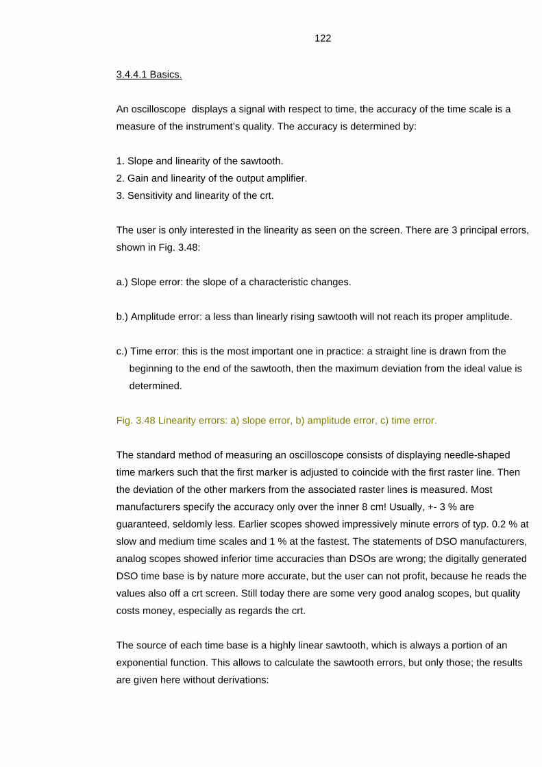
122
3.4.4.1 Basics.
An oscilloscope displays a signal with respect to time, the accuracy of the time scale is a
measure of the instrument’s quality. The accuracy is determined by:
1. Slope and linearity of the sawtooth.
2. Gain and linearity of the output amplifier.
3. Sensitivity and linearity of the crt.
The user is only interested in the linearity as seen on the screen. There are 3 principal errors,
shown in Fig. 3.48:
a.) Slope error: the slope of a characteristic changes.
b.) Amplitude error: a less than linearly rising sawtooth will not reach its proper amplitude.
c.) Time error: this is the most important one in practice: a straight line is drawn from the
beginning to the end of the sawtooth, then the maximum deviation from the ideal value is
determined.
Fig. 3.48 Linearity errors: a) slope error, b) amplitude error, c) time error.
The standard method of measuring an oscilloscope consists of displaying needle-shaped
time markers such that the first marker is adjusted to coincide with the first raster line. Then
the deviation of the other markers from the associated raster lines is measured. Most
manufacturers specify the accuracy only over the inner 8 cm! Usually, +- 3 % are
guaranteed, seldomly less. Earlier scopes showed impressively minute errors of typ. 0.2 % at
slow and medium time scales and 1 % at the fastest. The statements of DSO manufacturers,
analog scopes showed inferior time accuracies than DSOs are wrong; the digitally generated
DSO time base is by nature more accurate, but the user can not profit, because he reads the
values also off a crt screen. Still today there are some very good analog scopes, but quality
costs money, especially as regards the crt.
The source of each time base is a highly linear sawtooth, which is always a portion of an
exponential function. This allows to calculate the sawtooth errors, but only those; the results
are given here without derivations:

123
Time error = 1/8 slope error = ¼ amplitude error (3.24)
The maximum time error occurs in the middle.
There are two basic sawtooth generator circuits: the Miller integrator and the bootstrap
circuit; it can be shown that both are in fact identical. The Miller effect was already described.
Fig. 3.49 shows the principal circuits of a Miller integrator and a bootstrap generator.
Fig. 3.49 Principal circuits of a Miller integrator and a bootstrap generator.
Fig. 3.49a is the Miller integrator, consisting of a voltage supply V, a resistor R, and a
capacitor C in the feedback path of a simple op amp, here one transistor. The charging
current from V flows into C which is effectively increased to (1 + gain) x C. The output voltage
will linearly fall according to the relation dv/dt = I/C (I = current). The slope error is:
Slope error (Miller) = 1/gain x slope error (RC) (3.25)
As it is easy to realize a gain of some thousand, the error is thus reduced by that factor so
that extremely linear sawtooths can be generated. It is important to note that gain changes
are of no practical consequence.
The bootstrap generator derives its name from the man who pulls himself out of a swamp by
his own shoestrings. The reason why the sawtooth of a simple RC charging circuit is
nonlinear lies in the fact, that the charging voltage is reduced by the rising sawtooth voltage
thus reducing the charging current and hence the slope. If the charging voltage is delivered
by a floating battery riding on the output voltage, the sawtooth will be perfect. This is true with
the assumption that the source follower (or any other amplifier in its place) has the exact gain
= 1. This is practically unrealizable, even if a more complicated amplifier with the gain = 1 is
used. If the gain is < 1, the sawtooth will be underlinear, if the gain is > 1, it will be overlinear.
A simple calculation will demonstrate this: the gain of a Miller integrator may change by 5 %,
which is easily achievable. For the same sawtooth error the gain change of a bootstrap
circuit must remain < 0.02 %!
A further disadvantage of the bootstrap generator is the need for a control pulse of at least
the same amplitude as the sawtooth. Due to stray capacitances, e.g. of the disconnecting
diode, this generates an undesirable initial step in the waveform and thus a nonlinear
beginning of the time base. The author solved this problem by starting the bootstrap with a

124
small rectangle and stacking the sawtooth on top of this. For a Miller integrator only a start
pulse of an amplitude = sawtooth amplitude/gain is necessary.
However, faster sawtooths can be generated with the bootstrap circuit, also the retrace can
be much faster. In practice the advantages of both can be combined by stacking the
sawtooth of a Miller integrator on top of its charging resistor, this has the same effect as a RL
compensation.
3.4.4.2 Example of a complete sawtooth generator.
Fig. 3.50 shows the principal circuit diagram of the complete time base generator of an early
Tektronix scope.
Fig. 3.50 Principal circuit diagram of a complete time base generator (Tektronix).
The sawtooth generator proper is within the rectangle in the upper right part of the drawing.
The output signals are shown on the right-hand side:
- Sawtooth out to the horizontal output amplifier.
- Unblanking pulse to the crt grid control (Z axis) circuit.
- Trigger pulse to the vertical amplifier channel switching circuit.
The other parts of the drawing show the control section of the time base generator.
The explanation begins with the sawtooth generator. The amplifier of the Miller integrator is a
pentode which may be substituted by a JFET cascode, the reason for the tube is the high
amplitude desired. Later instruments replaced the pentode by a JFET source follower and a
bipolar transistor, the collector of which also has infinite impedance. A 75 V zener shifts the
potential via the cathode follower down to about zero volts. The reason is, that the ouput
amplifier must also accept external signals and thus is designed for zero input level. CL is the
charging capacitor which is switched in decade steps. Here only the very best capacitors
(Teflon, polypropylene, styrene, zero tc low dielectric constant ceramics) may be used which
show minimum dielectric absorption, see 3.3.4. Tektronix manufactured these in-house. As
these capacitors directly influence the time calibration, they must also be temperature and
long term stable. Customary values are 10 u for the slow sweeps and some hundred pF for
the fastest. Because of the extremely low charging currents at the slow sweep speeds (down

125
to 5 s/cm, equ. to 50 s total sweep time), special precautions are required to minimize
leakage currents, otherwise time errors or/and nonlinearities will surface. Also any dirt in this
area may cause the same problems, because dirt is always hygroscopic. Washing the whole
circuit will in most cases restore the good properties. After any wash switches and
potentiometers must be regreased. Only the switch contacts may be very lightly treated with
a contact oil, the isolating materials must not be treated.
A special problem is posed by the strongly varying charging current; it creates varying
voltage drops across the disconnect diode of a bootstrap generator and hence a shifting of
the beginning of the base line on the screen, disturbing during measurements.
The circuit shown contains one of the many fundamental inventions of Tektronix: In the
quiescent state a current flows out of the + 125 via the 68 K and both diodes such that both
remain conducting. This opens a dc path from input to output, i.e. this is an op amp with a
gain of one. Any potential change of the control grid potential by changes of the charging
current is amplified by the full gain of the tube and thus appears thus enlarged at the output.
It reappears through the other diode at the input with the effect that the control grid and the
output potentials remain stable and hence also the beginning of the base line on the screen.
A very small rectangular pulse is sufficient to cut off both diodes and to start the sawtoooth,
the charging current now flows into the capacitor, so the sawtooth starts.
This sawtooth start pulse is the result of a trigger pulse from the trigger pulse former circuit
discussed earlier. The pulse from the transformer switches the tunnel diode to its high state
which turns T6 on. Its collector goes to ground and pulls both diode anodes down. The whole
circuit is normally bistable, i.e. it remains in this state until the tunnel diode bias current is
changed via the 1.2 K resistor. Fig. 3.51 shows all the signals and will help in understanding
the circuit.
Fig. 3.51 Signals within the circuit of Fig. 3.50. Mode: normal, automatic off.
The central part of the time base control circuit is the Schmitt trigger composed of T4 and T5;
it has a wide hysteresis of – 3 to + 4 V. In the state „T5 conducting“ the collector current and
the tunnel diode bias currents are so adjusted by the potentiometer, that the tunnel diode is
set to just below its switching current. A trigger pulse, even short, will switch it to its high
state of ca. 0.5 V.
The rising sawtooth charges the hold-off capacitor CHO via D1. From the wiper of the
potentiometer „Sweep length“ a sawtooth is taken and applied to the base of T5 via D2. The

126
base is held to + 2 V by the divider 806 K – 9.76 K. As soon as the fraction of the sawtooth
minus the diode drop of D2 exceeds + 2 V, the base follows; when the upper hysteresis level
of + 4 V is reached, the Schmitt switches. T5 is cut off, the tunnel diode current drops to zero,
T6 cuts off, the potential at the diode anodes jumps, until the V 1 conducts. The 2 mA current
now generates the sawtooth retrace. As soon as the grid potential is reached, the output
stands still because V 2 conducts.
During the whole sweep and retrace time any further trigger pulses had no effect, because
the tunnel diode was in its high state anyway. They are still of no effect, because the tunnel
diode has no current. The circuit remains in this state, until the Schmitt trigger switches back
which is delayed by the hold-off capacitor. The reason for the hold-off is the output amplifier
which is often unsymmetrical, i.e. optimized for a linear sweep, its retrace time may even be
much longer than the fastest sweep time. No new sweep must be started until the amplifier
has completely settled in its quiescent position, and the trace has thus returned to its starting
position at the left of the screen.
The hold-off capacitor discharges slowly towards – 100 V; as soon as its potential decreases
below + 2 V + one diode drop, it pulls the base of T5 with it, until the lower hysteresis level is
reached. Then the Schmitt trigger switches back, the tunnel diode receives again its prebias
current from T5: the next trigger pulse can start a fresh cycle.
The crt in the type of scope from which this circuit was taken uses deflection plate blanking
(see chapter 2.1) with two pairs of deflection plates. As long as all plates are on the same
potential, the beam goes clear through to the screen. If a voltage is applied, the beam is
deflected so far off that it does not reach the screen any more. The main disadvantage of this
system is, that the beam is always fully on, even if the scope is not used, this is detrimental
to the life of the crt. The advantage is, that these plates are not on the high acceleration
potential (here – 3.5 KV), but on a low potential and thus can easily be driven from the
control circuit of the time base. V 1 is normally off, so that one plate of each pair is on + 300
V. For unblanking during the sweep V 1 is on, its anode potential is clamped to + 125 V
which is identical to that of the other two plates.
A negative square wave pulse of the same duration as the sweep is sent to the vertical
amplifier channel switching circuit, the negative slope triggers the channel switching which is
invisible.
Some of the signals in Fig. 3.51 show fine detail. A Schmitt trigger does not switch, until both
active elements draw current, constitute a positive feedback amplifier, and until the loop gain

127
exceeds unity. This is shown in „signal emitter T4, T5“; T5 draws already current before the
switching point, the common emitter potential decreases. After switching, the emitter
potential jumps by a small amount in positive direction, because T5 now draws all the
current, so that its Vbe increases a little.
In the mode „Single Sweep“, the connection between D3 and the base of T5 is removed with
the effect, that the time base control circuit can not return to its quiescent state after
completion of the single sweep. The circuit remains insensitive to trigger pulses, until the
neon is ignited by pushing the switch lever momentarily to the position „Reset“; the base of
T5 is pulled below the lower Schmitt trigger level, so that it switches back.
It remains to explain the „Automatic“ mode. As described earlier, all such circuits function in
principle the same: in the absence of trigger pulses the time base is set to its astable, free-
running state, so that the trace is well visible in all time base positions. As soon as a trigger
pulse arrives, the time base is switched to its normal, monostable mode. It is necessary to
set a limit for the time the circuit should wait for another trigger pulse before returning to the
astable state; usually, the lower limit of automatic operation is set slightly below 50 Hz.
In this circuit transistors T1 and T2 are connected as an emitter-coupled monostable. It is
also switched by a trigger pulse from a separate winding of the pulse transformer. If the
automatic mode is activated, T1 will be on and T2 off. T3 then is conducting and sends an
additional current into the emitter circuit of the Schmitt trigger which goes to the tunnel diode
via T5. The tunnel diode thus receives a current far above its maximum switching current (5
mA). The whole circuit is now astable, the tunnel diode switches immediately when T5
conducts.
If a trigger pulse arrives, the monostable will switch and disconnect T3, this causes the time
base control circuit to revert to monostable operation. However, as the arrival of a trigger
pulse is asynchronous to the time base astable frequency, it may take a full sweep period
until a sweep, synchronous to a trigger pulse, will be guaranteed.
There are scopes which are so poorly designed that in automatic mode parasitic „triggering“
may take place, caused e.g. by a poorly decoupled power supply etc., especially if the trigger
level control is set to its zero position which corresponds to maximum sensitivity. If parasitic
triggering occurs and a fast time scale was selected, the trace will become invisible. If this is
suspected, it is sufficient to turn the trigger level control from its zero (center) position, the
trace will then reappear.

128
3.4.5 Horizontal output amplifiers. Of the very many different designs Fig. 3.52 shows a fairly simple one, still symmetrical,
taken from an early Tektronix scope.
Fig. 3.52 Simple horizontal output amplifier (Tektronix).
It was already mentioned that such output amplifiers are generally unsymmetrical and
optimized for a linear sawtooth sweep. In fast scopes the retrace may take much longer than
the sweep. It is important to realize this and understand that a scope horizontal amplifier is
not well suited to amplify arbitrary signals, otherwise disappointments are programmed.
It shall be stressed that high performance scopes are generally unsuited for good XY
displays! Good XY displays may only be expected from scopes which were specifically
designed for that purpose and specified accordingly. It is deplorable that in schools still XY
displays, especially for phase measurements, are recommended. One should never perform
phase measurements this way! „Phase“ is just another word for time difference at a given
frequency. Such measurements are performed in 2-channel mode while triggering from one
channel; this way even minute time differences at high frequencies can be precisely – within
the limitations of a scope – measured. If one wishes to read the phase in degrees a full
period of the signal is exactly spread over the 10 cm by adjusting the „Time Variable“ control.
1 mm is then equivalent to 1/100 of 360 degrees i.e. 3.6 degrees. As the time bases of high
quality analog scopes are well within 1 %, the resolution may be further increased by
switching to a faster time scale. In order to get more precision, the scope may be overdriven
so that the zero crossings become more pronounced. If probes are used, both must be the
same type and same length, and it is necessary to first hook both to the same signal and
check for any time difference on the screen; minute differences in probe adjustment may
cause substantial errors at high frequencies! The capacitance adjustment of one (!) of the
two probes is then changed a little, so that the time difference is reduced to zero.
The unsymmetrical X amplifiers comply neither with the Gauss response nor do they feature
high bandwidth. XY measurements if at all necessary are hence strictly limited to very low
frequencies! Consult the manual first.
At the beginning of chapter 3.4 it was described that the horizontal amplifier receives either
the sawtooth A or B. The sawtooth voltage is taken from the low impedance cathode follower
output and converted to a current by the resistors in series with the emitter of T1, the
potentiometer is used for calibration. The emitter acts as a virtual ground or current sink so
that the sawtooth current and the current from the „Horizontal Position“ control are added.

129
The signal is taken off the collector of T1 and sent via the emitter follower T2 to one input of
the hybrid cascode difference amplifier. T3 cares for thermal balance. The output stage
combines the high transconductance of bipolar transistors with the high voltage properties of
tubes. The crt has a horizontal plate sensitivity of 20 V/cm, so that > 200 Vpp have to be
generated linearly. The switch „5 x Magnifier“ increases the gain by 5 and thus the time
scale. The amplifier is overdriven which is invisible as the beam hits the crt walls. In order to
avoid a dc shift when switching the gain, an adjustment „Magnifier Centering“ is provided
with which the potential difference between the emitters and the feedback resistors is set to
zero. This properly adjusted will cause the picture on the screen to expand from the center
both ways without shifting.
With all scopes which have an external X input watch out for screen burn if one inadvertently
switches to „External X Input“! A vertical line will show if there is a vertical signal, but only a
sharply focused spot if none, with the high intensity of modern crt’s the screen may burn
immediately. It is good practice to turn the intensity to zero, before switching to „External X
Input“.
All scopes achieve the fastest time scales only with magnification. In order to measure rise
times, the beginning of the sawtooth must be shifted onto the screen by adding an offset to
the horizontal amplifier. Here, some problems surface:
1. The beginning of the sawtooth is always nonlinear.
2. The X amplifier has a rise time and thus rounds the beginning of the sawtooth.
3. The X amplifier is being overdriven and this to one side, too.
Here the good scopes outdistance the poor ones! The trigger level should be set such that
rise time measurements are performed as far away from the beginning of the trace as
possible in order to stay clear from the nonlinear portion; due to the nonlinearity the sweep
speed there is lower, hence rise times will be measured incorrectly too short!
In order to test one’s scope for this, use a calibrated high frequency sine wave and adjust the
„Horizontal Position“ control: this will show any nonlinearity. Move the display over the whole
range of the „Hor. Pos.“ control and measure the sine wave period at several positions of it.
Some users may wish to get rid of their scope as fast as possible after this measurement...
3.5 Additional features.

130
3.5.1 Calibrators.
The minimum each scope must incorporate is a calibrator good enough (flat top, rise time < 1
us) to adjust customary 10 : 1 probes with an approximate 1 KHz square wave and precise
enough to check and readjust the vertical channel sensitivities. It is deplorable that few
scopes offer more than this today.
A calibrator just fulfilling the above requirements is inadequate to check and adjust the scope
input attenuators! A rise time of < 0.1 us would be required for this. Also, the amplitude must
be selectable over a wide range. Early high performance scopes had such calibrators, some
even with a crystal controlled frequency (1962!). Such a calibrator allows not only to adjust all
probes, including 1,000 : 1 high voltage probes, and all attenuator positions, but also the
basic time base calibration; this is all that is needed normally. Today, a cheap HCMOS ic is
all that is needed for fast, precise square waves; however, a precison divider and switch are
not to be had cheaply. The user could then detect easily, if the attenuators went out of
adjustment.
A further warning is given here: the long rise times of most calibrators not only do not allow to
test the attenuators, but neither to judge the scope’s rise time and are unsuited to adjust a
probe’s high frequency compensation elements! High speed probes contain typically 5
compensation elements, usually contained in the box at the scope input. The average user
may believe that a probe is adjusted after the 1 KHz basic adjustment was performed.
Nothing is further from reality. The 5 elements mentioned must be adjusted to the scope
input used and readjusted whenever another input is used! Otherwise gross pulse over- or
undershoots may be caused by the probe. Also, it is by no means to be expected that the
probes shipped with a new scope are adjusted to that instrument! For proper probe hf
adjustment first a suitable square wave generator is required. It is reminded here that
practically all „normal“ square wave generators are not good enough for this purpose, their
aberrations are too high. A second-hand Tektronix 106 ist the least expensive best choice; a
GR 874 to probe 50 ohm feedthrough termination is necessary, too. (See chapter 10 for
information about probes).
It is not that simple to check the amplitude accuracy of a calibrator. If the square wave is
derived from a toggle flip-flop and thus an exact 50 % duty cycle guaranteed (there is no
other way), a precision dvm will indicate the average value which is 50 % of the amplitude. If
the duty cycle is not exactly 50 % from a flipflop, this method is inappropriate. If the reference
voltage of the calibrator is accessible internally, this can be measured. A third method is the

131
construction of a simple peak reading voltmeter, however, this is impractical if the calibrator
amplitude is only some ten mV.
A simple but highly precise calibrator may be designed by using a 0.2 % or better reference
voltage ic (2.5, 5 or 10 V) which feeds a HCMOS Schmitt – Trigger (HC 14, 40106, 4093) –
RC astable multivibrator, precisely adjusted to 1 KHz. As the load is only a 1 M scope input
or a 10 M probe, the CMOS operates without load and is thus a precise analog switch to the
reference voltage and to ground. A 50 ohm resistor should be inserted in series with the
output. The rise time will be some ns and good enough for probe, attenuator and probe hf
adjustments. For the latter a higher frequency should be used so that changes in the rise
time area are visible. Adding a fast op amp with a precision divider all input attenuator
positions can be adjusted.
3.5.2 Readout. A screen readout appeared first with the Tektronix 7000 series mainframes. The characters
were generated with in-house ic’s as analog signals and time multiplexed with the signal
display. The sensitivites of 4 channels and the time scales of 2 time bases could be shown,
also information from other plug-ins such as spectrum analyzer, dvm, counter, curve tracer
etc. In certain time base scales the „holes“ created by the readout can be seen, it can be
switched off. A problem is the uniformity of focus over the full screen, with some instruments
it is either possible to focus on the readout or the signal. Thermal effects in the amplifiers
may also cause „breathing“ of the readout. This readout is handy ,because one does not
have to look at the fine print on the overcrowded small plug-in front panels, also the settings
will be on photos.
Philips once presented a very good solution which, however, was left later. To the right of the
crt there was a large LCD window on which all relevant data was displayed with large
characters. No precious crt screen area is lost to the readout which is disturbing with 4-
channel displays and all other disadvantages mentioned above are dispensed with. Philips
eventually used crt readout. Due to the excellent crt which is also used in all Hameg scopes
the readout is as well focused as the display.
3.5.3 t, Delta t, V, Delta V, f, period etc. These functions are dvm resp. counter functions ; there were also some scopes with set-top
boxes which contained a dvm or counter. As was mentioned already, all these functions were
standard and available out of series production in the 60‘s and do not constitute inventions

132
which came with DSO’s! Already then dvm and counter ic’s were standard items, so that only
a signal pick-off in the vertical amplifier was required; this should be at the input stage in
order to avoid an influence of the positioning, variable and invert controls.
It is so important not to be bluffed by the number of digits of digital displays! In this chapter it
was decribed in detail, why scope attenuators and amplifiers are by nature not very precise
and that no more than about 1 % may be expected. And even this is only achieved after a
thorough and accurate calibration. No 6 or 8 digit display can improve on this, regarding dvm
functions. As counters do not rely on amplitude accuracy a pick-off in a scope will not impair
accuracy.
The maxima and minima of a signal may be stored in peak memories, which are then defined
to be 0 and 100 %; all other measurements may refer to them, so also automatic rise time
measurements from 10 to 90 % are possible. There were special Tektronix scopes and
ancillary equipment (567, 568, 230 etc.) which could be assembled to complex automatic,
computer-controlled test installations e.g. for semiconductors etc., in the 60‘s, long before the
first DSO. The precision was far higher than possible with 8 bit DSOs.
3.5.4 Auxiliary inputs and outputs. Standard auxiliary inputs are:
- External trigger input
- External horizontal amplifier input
- External Z input (intensity modulation)
Today there are frequently auxiliary vertical inputs without attenuators, these can practically
only be used for logic level signals.
Standard auxiliary outputs are:
- Calibrator.
Earlier scopes also featured outputs for the sawtooths and gate signals of the time bases.
Some had outputs from the vertical preamplifier so that two channels could be cascaded for
higher sensitivity. The 7000 series had mostly also power supply outputs for FET probes and
other auxiliary equipment.

133
3.6 Power supplies. The first and most important rule for all electronics people is: first check the power supply!
Important note:
Scope power supplies, especially those of older instruments, operate with dangerously high,
potentially lethal voltages! The crt acceleration high voltages are mostly not as dangerous
because the power levels are low. Any work on an open scope must only be performed with
the scope connected to an isolation transformer. But this protects only from a connection to
the mains and not from the internal dangerous voltages!
3.6.1 Linear regulators. Within the scope of this book power supplies can not be covered, this would require a book
of its own. Here, only some aspects of scope power supplies are described.
Although the output voltages of high quality SMPS can be fully adequate to power most
circuits in a scope the performance of a linear regulator is unexcelled, especially for the
supply of high sensitivity analog circuits such as in inputs. The output stages can well do with
unregulated voltages.
Already the earliest high performance scopes derived their superior quality also from their
power supplies with linear (tube) regulators. Still today a scope needs several power supply
voltages, only the absolute values decreased in time. These sometimes very complicated
and interdependent supplies are not easily understood.
Basically, all voltages are derived from one voltage supply which also contains the reference,
this is predominantly the most negative voltage. The reason is that all voltages should ideally
be proportional, and that all should go to zero, if the reference should fail. Ideally a fault in
any supply should cause all voltages to go to zero, but this is rather an exception. It is
important, that all voltages should rise and fall simultaneously, otherwise a voltage may even
momentarily change polarity, which may cause destruction of components. Seldomly
protection elements against overvoltage, false polarity etc. are provided. Neither can it be
expected that all voltages are overload and short-circuit proof. Therefore care must be taken
when working on scopes in order to avoid overloads or shorts. This may cause defects and
high repair bills.

134
Historically and unchanged to this day power supplies belong to the circuits with the lowest
reliability. On the other hand, especially with today’s mainly digital scopes, the power supply
is one of the last areas of a scope where a repair is still possible. Due to the fact that some of
the linear regulators use voltages of other regulators, the search for the cause of a defect
may be cumbersome. The best course is to identify first the regulator with the reference and
start from there. If that should require other voltages, it may not function, because such a
voltage is missing. It is advantageous if the scope can be separated from its power supply.
However, it should be kept in mind, that some power supplies require a minimum load for
proper function and may malfunction when unloaded! If the circuit diagram specifies the
nominal load currents, dummy loads can be used.
If a scope and its power supply can not be separated, it is best to check all electrolytics and
semiconductors with the scope disconnected from the line and all capacitors discharged. All
semiconductors must be replaced to their original positions, otherwise a recalibration may be
needed. With older high performance scopes often corrosion of component leads,
connectors or grounding screws etc. is the cause. Another frequent cause is solder joint
recrystallization, a main problem of SMD, rarely mentioned. Each solder joint will recrystallize
with time, dependent upon the temperature reached in operation and the cooling velocity.
Such a solder joint displays varying resistance; if that is met there is no choice but to resolder
all connections in the whole area, because they will all be bad, not only the one identified.
A frequent cause of semiconductor failure is lost thermal contact. The old-fashioned but
wrong method of mounting power semiconductors was with a screw. It is long since known
that the case will then bend upwards, so that there is only a line but not an area contact to
the cooling surface. Also, the pressure will relax with time and so will the thermal contact,
especially if a plastic isolator is in between. The only correct method is a spring clip. When
replacing power semiconductors, of course, a spring clip can not be used, but then at least a
spring washer should be used with the screw.
One should especially focus on electrolytics, due to the cost pressure, here is one of the
areas where cheap and overloaded components abound! An overloaded electrolytic will dry
out with time which will impair the voltage quality and also may lead to wild oscillations.
3.6.2 Switch mode power supplies.
135
Modern scopes use practically exclusively SMPS of a wide variety of designs. He who is not
a specialist, should better refrain from touching these areas except in cases of obvious faults
like defective capacitors, shorted semiconductors etc.
In most cases a socalled flyback dc/dc converter is used which combines an impressive
assortment of advantages. Apart from the agreeable fact that it is the least expensive, it is
normally also a wide-range power supply, covering 105 (or even 85) to 254 V mains voltage.
Scopes always require several fairly well stabilized low voltages and the crt high voltage(s).
Here, one of the advantages of the flyback shines: the regulation loop can, of course, only
regulate one output voltage, but if the transformer (which in fact is not a transformer, but an
inductance with separate input and output windings) is well designed, all other output
voltages will also be quite well stabilized, obviating the need for postregulators.
The cause of problems are often wild oscillations. These may be provoked by defective
capacitors, mostly electrolytics. One must be careful with replacements if the original parts
are not available. It is very important to bear in mind that too good, i.e. too low ESR
electrolytics may also cause wild oscillations! Further, the ESR is temperature and age
dependent; a SMPS may oscillate when cold and stop when warm and vice versa. Such
regulation oscillations are mainly in the audible low frequency region, but it is good practice
to hook a scope to each voltage output and check for oscillations. With SMPS these can also
be dependent on the line voltage. The load in a scope, however, is practically constant.
The replacement of defective semiconductors is always critical if the original parts are not
available. The data sheet specifications are by far not sufficient to judge whether another
type may be suitable. Also, manufacturers continuously change the chips while leaving the
type designation and the data sheet unchanged, not only shrinking them which creates
thermal problems, but often they even change the technology, so a replacement may fail
although the type designation is identical! In such cases a transistor (mostly MOSFET) one
or two sizes larger might just be sufficient. This is the reality. The thermal contact is of prime
importance, but in off-line SMPS the main switching transistor is on line potential, so the
isolation material must also conform to safety standards, e.g. 1.5 KVrms test voltage to the
safety ground which mostly is connected to the cooling surface. A third, equally important
consideration is the fulfillment of emi standards; also in this regard the isolation material is
critical! Fourth, but not least, the isolation material should have low dielectric losses at the
switching frequency, otherwise it will heat up. Alumina filled silicone rubber of a thickness of
0.4 mm is a good choice. And: screws are out, spring clips are in, a reminder.

136
The high voltage(s) for the crt are seldomly also generated in the SMPS, since the first high
performance scopes in the 50‘s medium frequency sine wave oscillators are used.
3.7 Operation and control. 3.7.1 Direct operation. Direct operation of controls means that the user directly switches e.g. the input attenuator.
There was a „pushbutton religion“ which abolished all knobs, but decreasing sales enforced
the reintroduction of knobs for all important functions. Quite obviously, people advocating
„pushbuttons only“ never used a scope themselves.
Advantages:
1. Knobs for all relevant functions fit best the human hand, they can be grabbed „blind“, i.e.
without looking, and operated without forcing the user to take his eyes off the screen or
his measuring object. Screen readout of parameters helps.
2. Infinite resolution with potentiometers, e.g. for vertical and horizontal positioning.
3. Immediate reaction, no delay by microcomputers. Many, also extremely expensive
instruments show such delay, that it is impossible to operate them, unless the user forces
himself to wait after each touch of a control, until the microcomputer reacted.
4. All settings remain stored.
5. All settings can be read at one glance at the front panel.
Acceptable alternatives to knobs are pushbuttons for up/down control and a fast
microcomputer in conjunction with screen readout.
Disadvantages:
1. Today more expensive.
2. Switches for the attenuators and the time bases which directly switch signals are quite
bulky and require appreciable force for operation, also they suffer from wear and dirt
accumulation which may cause problems.

137
3. Poor quality potentiometers, to be found abundantly in highest performance top make
scopes, wear out and develop bad contact. This is a problem of quality only and not a
principal one.
4. Can not be remotely controlled.
3.7.2 Indirect operation. Indirect operation and the „pushbuttons only“ religion are not related. The main reason is
simply lower cost. Today, it is much cheaper to switch signals with analog switches or relays,
the cost of a microcomputer is zilch. If remote control is required, both are necessary
anyway. Nothing would speak against this advancement which it is, if at least the same level
of operating ease were achieved; the author could not find one scope where that was the
case.
Advantages:
1. Less expensive.
2. No wear of switches, potentiometers, no corrosion.
3. Controls require lower force.
4. Up/down pushbuttons possible.
5. Remote control at almost no extra cost.
Disadvantages:
1. Limited resolution, response mostly in jumps and jerks, delayed.
2. Controls are rotary encoders without stops and lettering; without looking at the readout the
user can not judge any more where the control is positioned nor can he turn a knob with
one movement to the correct or an approximate setting.
3. The „one look at the front panel“ information has gone; the user must work himself through
a menu with a multitude of submenus in order to find out many of the settings or to adjust
the scope. This implies the danger, that the user remains unaware of false settings. All
these efforts forced by menu control slow the work down and distract the user from the
main purpose of a scope.

138
4. Scopes designed according to the „pushbuttons only“ religion are unfit for normal use, so
are scopes with dozens of pushbuttons and one only knob which can assume dozens of
functions. „Bilnd“ operation, without taking the eyes off the screen or the measuring
object, is impossible: first the user must search among the dozens of pushbuttons to find
the one he needs now. During this procedure the user can neither loook onto the screen
nor on his object.
3.7.3 Remote control. Many, too many, recent scopes contain more and more expensive circuitry for an interface
than for the scope function proper: the tail wags the dog. No matter how poor the
measurement, but it can be sent via an interface. It is distressing for the expert to see the
cheapest components, assembled most primitively in the scope signal processing circuits,
but a pompous interface with expensive components. The test results of such instruments
are catastrophic, no surprise.
Remote control makes no sense for a scope in normal use, it is essential for scopes in
automatic test installations, but there the crt is superfluous.
An interface is helpful for screen printouts because these are fast and cheap. The intensity
information is lost as with DSO’s, but not always necessary.
Interfaces need no treatment here, they are extensively covered in the computer literature,
and knowledge about them is rather to be expected than any about scopes.
4. Analog storage oscilloscopes. 4.1 General remarks. Analog storage scopes are not manufactured any more since many years, but they are still in
use and available second-hand. In most applications they were replaced by DSO’s which is
justified. However, the statement of DSO manufacturers that DSO’s are generally better than
analog storage scopes is wrong. DSO’s are much less expensive in manufacturing, also
most of today’s „me-too“ DSO manufacturers never had the expertise for the complicated
storage crt’s nor the circuitry to go with them. One reason why DSO’s are much cheaper is
the fact that all DSO’s are sampling scopes, and sampling is nothing else but a frequency
transformation method, from GHz to some hundred Hz, consequently, cheap computer

139
monitors are fully adequate, require no knowhow, are manufactured in three-digit millions per
year, available to anyone.
Regarding performance, even the most expensive DSO’s can not touch a modern analog
storage scope. Advantages:
1. No false displays possible.
2. The same high signal acquisition rate, > 100 KHz, standard with all analog scopes. DSO’s
mostly just achieve 60 Hz, some up to 200 Hz, only some very recent types (Tektronix
DPO’s) reach the same acquisition rates, simply because a complete analog scope signal
acquisition is built in. All signal details which occur between two DSO acquisitions remain
unnoticed, DSO’s are blind between acquisitions and hence least suitable for catching
rare events! This extreme disadvantage of DSO’s is not mentioned by DSO proponents.
The probability to catch rare events with an analog storage scope is at least some 1,000
times higher than with the overwhelming majority of DSO’s.
3. In order to specify nice numbers, DSO’s must operate in the equivalent time sampling
mode, which requires that the signal repeats in absolutely the same shape (see chapter 5)
often enough to fill one screen; if the signal shape should change, the DSO representation
fails. When looking for rare events, this may take an extremely long time. The analog
storage scope requires only a single signal period.
Rare events, this is often interference, are not only irregular with respect to their repetition
but also to their shape and can hence only be caught by an analog scope or a DSO in real
time sampling mode.
Comparing now an analog scope with a DSO the latter must at least display 10 points per
cm; a 100 MHz DSO can just display one cycle of a 1 MHz signal with this resolution. The
fastest analog storage scope, the Tektronix 7934 (500 MHz) has a writing rate of 370
cm/us for a full screen, it can thus display a single event 15 MHz signal. A 500 MHz DSO
achieves 5 MHz at 10 points per cm. It requires a 2 GHz DSO to beat the analog storage
scope. But the analog instrument has an afterburner: in the mode with a reduced screen
area and increased acceleration voltage the writing rate speeds up to 2.5 ns/cm which
means that even a single event 200 MHz signal can be recorded, with 4 cm.
4. Analog storage scopes with transmission/transfer storage crt’s can store half tones, not as
well as a non-storage analog scope, but DSO’s lack this intensity information completely.

140
Z axis information is very important, especially when looking at malfunctioning circuits with
irregularly repeating signals of changing shape. The intensity shows clearly how often
different shape signals occur. With DSO’s all displays are evenly bright, there is no
information in the trace.
5. Further, analog storage scopes with the exception of the inexpensive simple bistable ones
can be operated in the „Variable Persistence“ mode, which replaces old by new
information in a controlled manner. Recent DSO’s try to emulate this function.
Disadvantages of analog storage scopes:
1. The storage time depends on the writing rate, it decreases to some ten seconds at the
highest. At low writing rates it may extend to hours. DSO’s excel here by infinite storage.
Also, DSO’s can manipulate and print the digitally stored information. Infinite storage with
analog scopes is only possible by photographing the screen. The quality is, however,
superior to a DSO printout.
2. Analog storage crt’s are very expensive, also the associated electronics circuitry. With
DSO’s storage requires no extra cost because a DSO is based on the signal storage by
nature. A replacement crt for a DSO is cheap.
3. Analog storage crt’s are easily offended by abuse! Burning is fairly easy. Also these crt’s
often show background images of earlier signals.
4. The usable screen area of fast storage crt’s is only 9 x 9 cm2; some crt’s attain their
fastest wiring rate only at a reduced screen area.
5. DSO’s can show recent and old signals simultaneously, they can manipulate stored
signals and also display the results.
4.2 Bistable storage oscilloscopes. The principle of these crt’s was explained in chapter 2.3. Their main advantage was low price
due to the simple construction. Already in 1963 Tektronix offered storage scopes with these
crt’s, they were very popular because of the attractive price. The crt was the standard 3.5
KV, 8 x 10 cm2 monoaccelerator type used in all low frequency scopes. The screen was
partitioned in half, both halves could be operated separately. A formerly stored picture could
thus be compared to a just stored one. Also it was possible to operate one half in normal,

141
non-store mode. The contrast was low, only 1 : 2, the storage time was about 1 h. There
were two types with different writing rates, 25 and 100 cm/ms, the latter had still lower
contrast. Scopes with these crt’s were manufactured until the 70‘s.
In order to beef up the writing rate, the crt could be operated in the „Integration“ mode, in this
mode the signal was stored several times over. As this method is not applicable to single
events, another mode „Writing Rate Increase“ was available: in this mode operating
parameters were changed so that the writing rate was increased at the cost of a lower
contrast and a shorter storage time.
It was possible to store several signals without erasing any. Normally, the crt was erased
automatically by the time base after each stored signal, this took appr. 0.25 s.
4.3 Transmission storage oscilloscopes. This oldest of all storage crt’s has been improved several times. In comparison to the simple
bistable crt it was expensive, but had these advantages:
1. Very much higher writing rate.
2. Half-tone storage.
3. „Variable Persistence“ possible.
4. Dark background.
5. High contrast.
Dependent on the choice of potentials a transmission crt may be operated bistable or half-
tone. The intensity of the stored display may be exchanged for storage time (view time). The
electrons from the flood cathodes create also positive ions which cause the background to
increase in brightness with time; by reducing the flood cathode current (duty cycle
modulation) the best compromise may be chosen.
Instead of erasing the screen completely, the erase pulses may be duty cycle modulated.
When displaying slowly repeating signals, which normally cause a flickering display, the
erase rate can be adapted to the signal such that an almost continuous, stable display is
obtained. The expression variable persistence denotes this accurately: if erasing is too
strong, the slowly moving signal will flicker annoyingly, comparable to a screen with a long
persistence phosphor. If erasing is too light, further signal displays will overwrite the stored
display, this will cause broadening of the trace or, if the signal changes its shape, a smeared
display. If the persistence is just right, a stable display will result, and changes will be visible.

142
4.4 Transfer storage Oscilloscopes. The transfer storage crt resulted from the interchangeability of writing rate and view time. In
front of the storage screen proper a mesh is mounted which is coated with a dielectric
optimized for high writing rate. The beam writes onto this mesh, and, before the stored image
has disappeared, it is transferred quickly onto the second storage screen which may be
operated bistable or with variable persistence.
Typical representatives of scopes with such crt’s were the Tektronix 7834 and 7934. By
suitable choice of potentials these scopes offered 4 operating modes:
1. Fast Variable Persistence: highest writing rate (7834: 300 div./us (2.5 ns/cm with reduced
screen area 4.5 x 4.5 cm2).
2. Fast Bistable: 7834: 50 div./us.
3. Variable Persistence: 7834: 2 div./us.
4. Bistable: 7834: 0.03 div./us.
To the author’s knowledge there were no further scopes with such crt’s after the 7934.
All analog storage scopes suffer from two disadvantages compared to non-storage scopes:
the screen area is only 9 x 9 cm2, and the non-storage intensity is far lower than that of non-
storage crt's, because storage crt’s can not operate with the high acceleration voltages of
regular crt’s (up to 24 KV). The 7834 reaches 10 KV.
Ende Kapitel 4.

143
5. Sampling Oscilloscopes. 5.1 History Physical laws can not be abolished or sidestepped. Sampling oscilloscopes were the fastest
oscilloscopes and this will not change; hence leading manufacturers are still offerring them
and even at an increasing rate. They were not outmoded by „modern“ DSO‘s nor
outdistanced. Recent sampling oscilloscopes sport 70 GHz and more, far above DSO‘s
which presently reach a few GHz. This enormous difference in performance requires
extensive treatment of sampling basics, also, because this chapter is the foundation of the
following one about DSOs. All DSO‘s are sampling scopes, but due to their additional
problems of a/d conversion and reconstruction the quality of their of signal representation
must remain markedly inferior even to that of the oldest sampling scopes!
The author’s intent is to outline that sampling technology is by no means a recent invention
of DSO‘s, inspite of manufacturers‘ statements, but indeed very old.
Sampling is based on the stroboscopic effect, the first instrument of this kind was built in
1880 by Joubert, it was used to look at the waveshapes of voltage and current of an ac
generator. It was hence a true oscilloscope, however, still without a crt.
The servo system was invented in 1898 by Callender. The „Ondographe“ by Hospitalier of
1904 was manufactured for decades; also this instrument like all others of that time was only
usable for line frequency phenomena.
1950 Janssen of Philips built a 50 MHz sampling scope based on a 50 KHz scope, only for
sine waves.
1952 McQuen of the British company Vickers contributed the advanced random sampling
method. He is the inventor, there is no debate, he realized the advantages and
disadvantages; his instrument possessed already almost all features of modern random
sampling scopes , e.g. it used an automatic servo system for the optimum distribution of the
sampling pulses.
1957 Sugarman invented the first sampling scope for nonsinusoidal waveforms.

144
HP presented in 1960 the first sampling scope which was manufactured in series (185A +
187A, 500 MHz, 10 mV/cm). HP remained in the lead for some years and offered the first 1
GHz sampling scope in 1962, it was equipped with 2 sampling probe heads; 1964 followed
the first 4 GHz instrument , 1966 the first 12.4 GHz type.
Tektronix had missed the train, but took the lead from 1967 with the first practically usable
random sampling scope (3 T 2 plug-in for the 560 series mainframes). The bandwidth was
initially 1 GHz (with the companion plug-ins 3 S 76, 3 S 1), then the 3 S 2 vertical plug-in
appeared which accepted 2 small socalled sampling heads. The first heads featured 1, 4,
and 14 GHz. This level of performance remained unexcelled until some years ago.
Already in 1970 special plug-ins (3 S 5,6; 3 T 5,6 etc.), mainframes (567 + 6R1, 568 etc.)
and ancillary instruments (230 etc.) were available from Tektronix which allowed the
construction of small and large automatic test installations which performed digital high
resolution precision measurements, also in conjunction with minicomputers like the famous
PDP-8. These instruments were not limited to 8 bits of resolution like nearly all of today’s
DSO‘s, but they contained high resolution, highly accurate sawtooth or dual slope a/d
converters of far superior quality! The automatic measurement of parameters such as:
amplitude, relative amplitude, time, time difference, frequency, period, rise and fall times,
limits etc. was standard and is definitely not a recent invention introduced with DSO‘s which
is falsely claimed. Also, these instruments of the 70‘s used, of course, transistors, linear and
digital ic’s.
Preempting the following treatment, it should be emphasized that sampling scopes are fully
equivalent to analog scopes as regards the vertical resolution, this is only limited by the crt or
postprocessing circuits. The real amplitude is displayed, not an a/d converted, stored, d/a
converted and reconstructed one.
Already the instruments introduced before 1967 featured real time sampling and fm of the
sampling frequency in order to break up false displays. Another standard was the possibility
of high resolution, high accuracy records on XY plotters, far beyond the quality of all DSO
print-outs.
5.2 Application of Sampling Oscilloscopes (SO’s) and DSO’s. The „normal“ oscilloscope buyer or user can choose between analog scopes, sampling
scopes, and DSO’s. Lacking special scope knowhow he is lost. The essential differences

145
between analog scopes and DSO’s will be treated in chapter 6. Which are the most important
differences between SO’s and DSO‘s? This is only intended as a concise preview.
5.2.1 Common characteristics
SO’s and DSO’s use sampling in order to convert a high frequency signal to a low frequency
signal; sampling is equivalent to mixing or multiplication and the only method to reach
bandwidths unattainable with any other at the expense of time (= signal repetitions).
5.2.2 SO‘s
A SO samples the signal directly at the input, the amplitude resolution is identical to that of
an analog scope and hence infinite. In fact sampling scopes are analog scopes. No
bandwidth limiting circuitry precedes the sampling bridge, so the high bandwidth combines
with high sensitivity of typically 1 mV/cm. The signal is processed and stored by analog
circuitry, the output is an analog low frequency voltage signal replica of infinite amplitude
resolution which can be displayed on a crt , plotted on a XY plotter or further processed.
It is very important to realize that a SO uses only sampling and nothing more; it suffers hence
only from the inherent problems caused by sampling, it is free of the multitude of additional DSO problems! Consequently, many false DSO displays are impossible with
SO’s. E.g. SO’s as analog scopes do not use „interpolation“ by drawing lines between a few
isolated sampling points; if there are too few sampling points, this will be obvious with a SO,
while the interpolation of DSO’s obscures this fatality and thus can lead to grossly false
displays.
All inputs except the probes are 50 ohms at 1 .. 5 mV/cm. Attenuation requires the use of
external 50 ohm attenuators. High amplitude signals can only be measured using high
dissipation, high bandwidth attenuators which constitute a sizeable load. FET probes with 50
ohm outputs are possible, but they limit the bandwidth, presently to a few GHz. Passive high
impedance probes can not be used with SO’s. SO’s excel, however, by the availability,
already with the earliest SO’s, of sampling probes. Here, the sampling bridge is contained in
the probe with a typical impedance of 100 K and a few pF. The probe can be directly hooked
up to the test object; the dynamic range is the same as with a 50 ohm input: a few volts. The
bandwidth of sampling probes was 1 GHz.

146
The output signal is analog, any digital use requires a/d conversion. But there is a vital
difference to DSO’s: there are only very low frequencies to be converted, so high resolution
converters can be used.
5.2.3 DSO’s.
Basically, a DSO is a sampling scope with an analog front end including attenuators, a fast
a/d converter, a fast memory, digital signal processing, reconstruction, and display
electronics. Its applications and its operation are similar to analog scopes, hence they are
almost as universal and in this respect superior to SO’s.
In contrast to a SO the sampled signal is immediately a/d converted. The analog front end
limits the bandwidth to, at present, a few GHz. The very much higher (up to 100 GHz)
possible bandwidth in the ETS mode remains reserved to SO’s which sample the signal
directly. The next enormous difference is the low 8 bit resolution of the fast converters.
Any digital data transmission, storage, manipulation requires prior a/d conversion. Each a/d
converter needs a certain conversion time, hence a lossless conversion is impossible. Due to
the conversion time necessary, only samples of the signal can be taken in intervals which
have to be stored in an analog memory for the duration of the conversion. In many cases,
e.g. telephone, a reconversion to an analog signal is required. In these cases the (de)tour via
a/d- and d/a conversion contributes three serious impairments of the original signal! Precisely
speaking there are then five causes of deterioration because of the additional quantization
and many other errors of the a/d and d/a converters. Looking at the facts without euphoria or
bias it is evident that any conversion of a signal into a digital representation causes loss of
quality, deterioration and introduces distortions and artifacts which were not present in the
original.
Even a very fast a/d converter is of limited value, because the data converted must be
stored, and any memory will be eventually full. Then the data stored must be digitally
processed and displayed; during this long time a DSO is blind to the signal! This is a serious
disadvantage. A modern analog scope like the Tektronix 2467 easily displays a signal
500,000 times per second, even the oldest analog scopes achieved 100,000 times. Except
for the Tektronix „DPO’s“ all DSOs capture the signal only some ten to some hundred times
per second, several orders of magnitude less! (DPO’s additionally contain most electronics of
an analog scope.) DSO’s thus are the least appropriate for capturing rare events – contrary
to manufacturers‘ statements!

147
5.3 Basics of sampling. 5.3.1 Common characteristics of the sampling methods. The first important fact to bear in mind is the data loss resp. reduction which is caused by
sampling. This is quite evident when visualizing that one can draw an infinite number of
curves or waveshapes between widely spaced sampling points. Another way of putting it is
that an infinite number of different signal waveshapes exist, which have the same sampling
points in common, i.e. will yield the same sampling points.
Here, many will ask: what does the socalled Nyquist theorem mean; according to this a
signal can be reconstructed if it is sampled with a frequency at least twice as high as the
highest frequency contained in the signal. The necessary precondition for this to be true is
mostly forgotten to mention: the signal to be sampled must first pass through an antialiasing
filter which cuts all frequencies completely off which are above half the sampling frequency.
The Nyquist theorem in reality includes prior knowledge about the shape of the signal: it is a sine wave! Any signal may be represented by the fundamental and its harmonics
while conserving their respective time/phase relationships. Hence the highest frequency in a
signal is a sine wave.
This can be easily demonstrated on any SO: sampling a sine wave at twice its frequency will
result in one sampling point at the left of the screen and one at the right, that is all: any
number of waveshapes may be drawn through these two points. Only because one knows
beforehand that is must be a sine wave, this waveshape can then be drawn through the two
points.
Quite obviously, no signal can ever be recognized by just two points on the screen; even a
coarse approximation to its true waveshape would require 1 point per cm which means
nothing else but 10 times the „Nyquist“ sampling frequency! For an acceptable representation rather 10 points per cm will be necessary, this requires 100 times the Nyquist sampling frequency, and this is the reality! Or, when using ETS, that many more
signal periods are required for one reconstruction with that resolution. In the author’s opinion
there is no other theorem in electronics more severely misunderstood and misapplied than
the Nyquist theorem!
Our topic is oscilloscopes. In chapter 3.3.1 it was explained that any scope must have a
Gaussian frequency response and flat group delay. This requirement contradicts fully the
Nyquist theorem which asks for a socalled brick wall filter at half the sampling frequency, an

148
„ideal low pass“ which is not realizable. But any real filter with such behaviour creates terrible
signal distortions, totally unacceptable not only in any oscilloscope but also in all other areas
like high fidelity! True fidelity means clean pulse response, i.e. all components of a hifi
system must absolutely have the same response as an oscilloscope! Now we have learnt
that the Gauss response falls off very early and gradually, any sharper roll-off causes pulse
distortions. It follows that the cut-off frequency of an antialiasing filter must be far higher than
the system’s – 3 dB point, this in turn means nothing else that the minimum sampling
frequency must be far above the „Nyquist frequency“! We are thus again at a minimum practical sampling frequency of 10 to 100 times Nyquist!
And because this simple fact was known e.g. to (some, not all) designers of early tape
recorders, good ones used 126 KHz in the 50‘s. Except for some early poor machines all
tape recorders used at least 100 KHz. The ac bias analog tape recording is nothing else but
a sampling system. The bias field is typically 10 times as strong as the signal field, the signal
is recorded each time the bias field falls below the critical magnetic field strength. And
because this simple fact obviously was not known e.g. to the designers of the CD and similar
systems, their sampling frequencies (44.1 KHz) are much too low, which is slowly being
understood and accepted in the course of the last years. People were abstonished that 96 or
192 KHz produced an audibly better sound – this should make no difference if the Nyquist
theorem would apply, but it does not. Of course, a good portion of the distortions of CD’s is
due to the steep filters used and a/d-, d/a converter and reconstruction errors.
If the Nyquist theorem is violated, beat frequencies between the signal and the sampling
frequency are created. As mentioned in the introduction, sampling is nothing else but using
the stroboscopic effect or mixing or multiplying. This is easily shown on any SO: with some
effort at synchronizing a signal frequency with the sampling frequency or a fraction thereof:
the beat frequency can be seen; if both are quite stable, such a false display may stay for
some time.
Returning to oscilloscopes, it is evident that antialiasing filters with Gaussian response and
flat group delay are at best difficult to realize up to several hundred MHz and close to
impossible into the GHz region. Hence as far as is known no SO and maybe few DSO‘s have
any such filter incorporated. The consequence of the lack of an antialiasing filter is clear: the
minimum sampling frequency must be far above the highest signal frequency component, not
fundamental.
The difficult topic of signal reconstruction will be treated in chapter 6 as it is of no importance
with SO’s except for the special case of single event SO’s.

149
Sampling implies analog storage, this is basically pulse stretching, also called sample-and-
hold. Sampling extracts energy from the signal and thus distorts it already.
In practice two methods are used:
1. A switch between the signal source and the storage capacitor is closed for a short period.
2. The switch is normally closed, the voltage on the capacitor follows the signal; in the
moment of sampling the switch opens, so the capacitor holds the last signal amplitude.
Fig. 5.1 shows the principal circuit, a second switch S 2 discharges the capacitor as soon as
the stored amplitude has been processed.
Fig. 5.1 Simple sampler with reset. Principle of the ealiest SO’s.
Two remarkable facts become evident:
1. During the sampling time the signal is averaged by the Ri x Cs time constant.
2. All signal details between sampling points are lost foreever!
If a sampling frequency far above the highest signal frequency is used, a series of needle
shaped pulses is obtained, the envelope of which represents the original signal. Low pass
filtering removes the sampling frequency and its harmonics, so that the approximate signal
shape is obtained. Without filtering the signal frequency band will be encountered on both
sides of the sampling frequency and its harmonics as is the case after mixing or modulation
of two frequencies. Hence sampling, mixing, modulation, multiplying are essentially the
same. This is easily understood by remembering that a mixer or modulator is nothing else
but a switch which lets the signal pass at the rate of the oscillator (= sampling) frequency.
And this explains without effort the creation of beat frequencies (aliases, ghosts, artifacts).
The purpose of mixing in a radio or tv receiver is the same as here: transformation of the
input signal into a frequency range (IF) where it is more easily amplified. In a receiver the
information is in the AM or FM of the signal, only this modulation is eventually extracted and
used, the frequency (carrier) is in principle immaterial.

150
In contrast to this the purpose of sampling is to reconstruct the signal shape. There are
applications of sampling where only certain signal parameters such as its rms, voltage
amplitude, actual power values are desired; here, other conditions rule and undersampling is
allowed, provided precautions are taken to detect any upcoming beat frequencies and to
change the sampling frequency upon such detection. Used e.g. in power analyzers.
Fig. 5.2 shows the influence of the sampling pulse duration. A sampling pulse of duration tau
samples the signal, a square wave, at three different times t1 to t3. During the closing
interval of switch S1 the average of the signal vi(t) will be stored on Cs. The resulting output
signal vo(t) is a linear rise from 0 to 100 % of duration tau. As the rise time is defined from 10
to 90 %, the rise time follows from the duration of the sampling pulse:
tr = 0.8 x tau (5.1)
Fig. 5.2 Influence of the sampling pulse width on the rise time and the waveshape.
In case of a sinusoidal input signal the following function is obtained, which is known e.g.
from tape recorder reproducing heads or movie sound track reproduction:
sin (pi x f x tau)/(pi x f x tau) and: fc = 0.44/tau (fc = cut-off frequency) (5.2)
Evidently, the result will be zero if one signal period or a multiple thereof fits exactly in a
sampling pulse duration window. Also, the result may be negative if the average at the end of
the sampling pulse duration happens to be negative.
First-class samplers like the Tektronix S1 sampling head indeed show precisely the pulse
response depicted in Fig. 5.2. Obviously, this response does not correspond to the pulse
response of a Gauss system.
In spite of this the already known equation is also valid for SO’s:
tr x fc = 0.35, because 0.35 = 0.8 x 0.44 (5.3)
Fig. 5.2 shows another important characteristic of sampling systems: the sampling efficiency.
The charging of Cs via Ri follows the known exponential, it thus depends on tau, Ri, Cs, to
which voltage level Cs will be charged at the end of a sampling pulse. The efficiency eta
follows from:

151
eta = (vo(to + tau))/(vi(to)) = 1 – exp (-tau/Ri x Cs) appr. tau/Ri x Cs (5.4)
The efficiency of customary SO’s is 3 .. 25 %, it is constant for instruments with 50 ohm
inputs; with sampling probes it will depend on the internal resistance of the signal source.
The efficiency decreases with increasing bandwidth. Changes of the sampling pulse duration
will affect the output voltage directly.
5.3.2 Real Time Sampling (RTS). The oldest and general sampling method is real time sampling, this expression is somewhat
misleading and today heavily abused in order to make potential buyers believe that a DSO
operates in „real time“ like an analog scope!
Real time sampling means that a signal that may be a single event, may repeat in irregular
intervals or periodically, that never reoccurs with the same shape like music or speech is
sampled with a frequency which at least fulfills the Nyquist theorem so that is can be
sufficiently reconstructed.
Obviously RTS does not represent any advantage for an analog or sampling scope. If this
mode was offered in SO’s, it was for another reason: SO’s are sensitive by nature, around 1
.. 2 mV/cm. In the past there existed pure sampling scopes, which were basically not
applicable to low frequency measurements such as the ripple on a power supply. In order to
allow users of such instruments low frequency measurements, RTS was added, the sampling
frequency (100 KHz) was frequency modulated by the line frequency in order to break up
false displays.
RTS is treated in detail in chapter 6.
5.3.3 Single Event Sampling. This chapter treats single event SO’s, not to be mixed up with DSO’s! Also here it applies
that the capture of single events did not see the world’s light first in DSO’s, but was invented
long ago as well as a/d conversion, automatic measuring of signal parameters, ETS, RTS
etc.
The author described two methods of capturing single events in an internal paper at the
Technical University of Aachen in 1965:

152
1. Circulation of the single event pulse in a delay line, after each circulation a sample is taken
with ETS; by the circulation the recurrence, necessary for ETS, is achieved. By suitable
switching, the pulse is conducted into the delay line, then the input disconnected.
2. Construction of a delay line with a large number of taps for sampling bridges with
associated electronics and analog memories, e.g. 100. It is possible to turn these
samplers on either synchronous with the signal or successively in or counter to the
direction of the signal. This allows to change the time scale. The contents of the 100
analog memories is read out with a sufficiently high frequency above the flicker limit and
displayed on a screen. The amount of hardware may seem high at first sight, but it was
already at that time possible to put the whole signal processing circuitry for one sampling
channel onto one chip. The bandwidth of such a system is only limited by the bandwidth of
the delay line, by the samplers, by the losses of the delay line, by the energy loss caused
by the signal extractions, and by the socalled sampling kick-back. At that time already 4
GHz feed-through samplers were standard; a scope with a bandwidth of at least 1 GHz or
0.35 ns rise time could have been built. A DSO with 5 GSa/s allows 50 MHz single event
capturing with 100 points, that is 1/20th , which demonstrates again the „advancement“
claimed by DSO manufacturers some 30 years later and reduces this „advancement“ to
the correct dimensions. The single event sampling scope has infinite amplitude resolution,
compared to a coarse 8 bit a/d converter, and surpasses the DSO also in this respect by
far! The author’s work was continued by colleagues (Schwarte et. alii) and was the
foundation of several dissertations.
5.3.4 Equivalent time sampling (ETS). In the introduction it was already mentioned that the SO is based on the stroboscopic effect,
and it was initially named accordingly. Sampling is a frequency-to-time transformation of the
signal which may be best visualized by looking at the socalled „information volume“ shown in
Fig. 5.3.
Fig. 5.3 The principle of sampling visualized by deformation of the shape of the information
volume.
The information volume is given by the three axes time, amplitude, and bandwidth. It may be
deformed in principle at will, provided the contents, i.e. the information, remains constant.
The drawing shows a given information volume shaped initially as a cube of volume V. The
stroboscopic sampling deforms this shape such that the amplitude remains unaffected, while
the bandwidth is reduced by the same factor the time is increased.

153
Two preconditions must be met in order for ETS or RS to function:
1. The signal must repeat as often as is needed to reconstruct it once.
2. The form or shape of the signal must not change during the reconstruction time.
The sampling pulses are controlled in such a manner, that one sample is taken from each
signal period; the sampling pulses are delayed from period to period – by equal amounts with
ETS – so that, after completion of one reconstruction cycle, the same effect is achieved as if
all samples were taken with a very high sampling frequency from one period of the signal. It
shall be mentioned already here, that traditionally SO’s operated with a maximum „sampling
frequency“ of 100 KHz, as appr. 10 us were required for processing of the samples. If the
signal frequency is higher, periods will be left out as usual with an analog scope.
Fig. 5.4 will give an insight into the functioning of a SO by showing the relevant signals.
Fig. 5.4 Relevant signals within a sampling scope in ETS mode.
The precondition for the sampling pulse delay proceeding from signal period to signal period
is a stable trigger derived from one and the same point of the signal. This way also signals
which do not repeat regularly can be sampled, the same as with analog scopes. In principle it
may take any time for one single reconstruction of the signal; the practical limit is set by the
drift of the analog memories.
The sampling pulse delay increasing from trigger to trigger is realized by each trigger starting
a socalled fast ramp. A comparator compares the amplitude of the fast ramp with a staircase
signal which is increased by one step from sample to sample. The fast ramp thus runs a bit
longer from sample to sample, because the next staircase step became higher. The
comparator switches hence later by from sample to sample by equal time increments and
triggers the sampling pulse generator in the vertical channel: this is exactly the same
procedure as with a stroboscope.
The time increment T is the decisive parameter by which the sampling pulses are delayed: it
is the „equivalent time scale“. As mentioned, a standard SO can not sample more often than
each 10 us. In real time, the individual sampling points of a reconstructed signal period on
the screen are thus spaced 10 us or longer. If, e.g., a reconstruction on the screen consists
of 100 points, the SO will need 100 x 10 us = 1 ms or more to fill the screen once. The real

154
time scale would thus be 0.1 ms/cm, but this is only important for the SO design, not for the
user. Relevant to the user and written on the front panel is only the „Equivalent Time Scale“
from which the ETS method derives its designation. This is the time scale relative to the
signal, the time increment T. Because the user reads the time scale from the raster, the
time/cm is calculated by taking the number of points per cm into account. Hence, if T = 1 ns,
and if 10 points/cm were selected, the time scale will be 10 ns/cm.
By decreasing the height of the staircase steps, T resp. the time scale can be shortened
down to zero which means an infinite expansion; at infinity, always the same signal point will
be sampled: there will appear a horizontal line on the screen the height of which depends on
the amplitude at the trigger point selected. This is just typical of the stroboscopic method and
does not constitute a special performance! Consequently, a SO with a shorter minimum time
scale is no better than another – this is contrary to the performance of analog scopes! As
with any oscilloscope, a short time base is only meaningful in order to display its own rise
time well; with SO’s the rise time is determined mainly by the sampling pulse width and
parasitic elements in the signal path.
What are then the performance requirements on the various electronic circuits in ETS mode?
Because the samples can not occur more often than each 10 us, a rise time of 2 us will be
sufficient for the vertical amplifier, this is equivalent to a bandwidth of 170 KHz. The fastest
real time scale was mentioned to be 0.1 ms/cm, which means a horizontal sawtooth duration
of 1 ms. Both can be realized with most moderate means. Assuming the signal frequency to
be 1 GHz (- 3 dB), this is to be compared to the appr. 200 KHz vertical amplifier bandwidth,
the ratio is 5,000. Hence this is the factor by which the signal frequency was transformed.
How many signal periods were required, depends on the sampling point density resp. the
quality of the reproduction. At 100 points per screen and 10 us a full screen requires 1 ms;
during this time the 1 GHz signal counted 10exp-3 x 10exp+9 = 10exp+6 periods of which
only 100 periods were used which correspond to the 100 samples displayed. If the quality is
lifted to 1,000 points per screen this will require 10 ms and 10exp+7 signal periods.
This is a very important aspect which shall be looked at from still another viewpoint. First we
should keep in mind that a SO like an analog scope has infinite vertical (amplitude)
resolution, the resolution is practically limited only by the screen resolution, i.e. trace focus
and screen area. It is far superior to that of any DSO (apart from some special DSO’s with
higher resolution a/d converters for low frequency applications which are not competitive
here). Because the samples obtained in the ETS mode are fully equivalent to those derived
from a single signal period, 1,000 points per signal period (assuming one signal period fits
exactly on the screen of 10 cm) at a signal frequency of 1 GHz are equivalent to an

155
(apparent) sampling frequency of 1,000 GHz! Let the buyer beware: such figures are today
common in DSO propaganda; of course, any DSO can be operated in ETS mode! Too easily
such a figure may be misunderstood by the non-expert buyer or user as a performance
specification and mixed up with the true sampling rate the DSO is capable of!
100 points per cm is equal to 1 point per 0.1 mm, considering that most crts‘ traces are
wider, this resolution already looks like a continuous trace. In short: a SO offers a signal
quality comparable to an analog scope and thus is far superior to any DSO. SO’s are
absolutely free from all DSO defects caused by a/d, d/a conversion, 8 bit resolution,
interpolation and other reconstruction distortions and artifacts. And this superiority of SO’s
dates back to the 60‘s.
As a logical consequence of the preceding paragraph it follows that a SO can sample a
signal also at any arbitrary low rate; the sampling may be controlled by hand or from a
plotter, e.g. Even the oldest SO’s had an analog output for plotters, so that the screen display
could be plotted with extremely high resolution. Screen printouts are thus an old story and no
invention of DSO’s. Also, the enormous difference in quality between a crude „modern“ DSO
printout and an analog plot, e.g. in A3 format, must be considered.
Last not least: let us take a look at the manufacturing cost of both. Compared to a DSO the
hardware cost of a SO is minute! Consequently, DSO’s are very much more expensive than
SO’s. This price difference becomes still more pronounced, if one compares the cost of a
pair of sampling plug-ins for an analog scope with the price of a DSO!
DSO’s are superior to SO’s in just two aspects: single event monitoring and flicker-free
display of signals with low repitition rates.
Another subtle difference between analog scopes, SO’s and DSO’s is the lack of Z axis
information with both the latter: all samples are of equal intensity. With analog scopes the
trace intensity relates important information about the speed of the signal or portions thereof.
It must be stressed that the stringent ETS mode requirement (the signal must repeat in the
same shape as often as is needed to complete a reconstruction) precludes the use of SO‘s
as well as DSO’s (in ETS mode) in many practically important applications! Examples: wild
oscillations of circuits, unstable circuits, stochastic breakthroughs of semiconductors,
modulated signals, oscillations with increasing or decreasing amplitudes etc.

156
After the explanation of the principal functioning of sampling, the signal processing will be
treated. Janssen used a lowpass for the recovery of the sampled signal because his scope
was only for sinusoidal signals. This was no longer possible in the first triggerable sampling
scope, because this was intended for arbitrary, non-sinusoidal, non-periodic signals. Now a
memory was needed, a socalled zero-order element. This function is already fulfilled by the
storage capacitor Cs in Fig. 5.1, but the two requirements: high sampling efficiency = small
capacitor, and a long storage time = large capacitor contradict each other. At first, several
amplifier stages with a capacitor in each for pulse stretching were introduced. These SO’s of
the first generation suffered from various disadvantages: before a new sample was taken, all
these capacitors had to be discharged, with each sample the first capacitor had to be
charged again to the signal level, even then, when this new level was identical or nearly
identical to the former one. This caused high energy extraction from the signal and a high
reflection coefficient. The sampling gates were simple diode or transistor circuits with
moderate linearity which sent a sizeable socalled sampling kick-back to the signal source.
At the beginning of the 60‘s symmetrical sampling gates and servo systems in the vertical
channel became standard; these were the innovations which upgraded the sampling scopes
to true measuring instruments.
Fig. 5.5 shows the principal circuit of a servo system which is valid for all SO’s.
Fig. 5.5. Principal circuit of a servo system in the vertical channel of a SO.
The input signal is routed via a symmetrical four diode gate to the input capacity of a source
follower. The next stage is an ac amplifier which, as will be explained later, is sufficient as it
only has to amplify the changes from sample to sample. Thus there are no dc drift problems.
The output of this amplifier is gated into an analog memory which may be a capacitor with a
source follower or a Miller integrator. The latter is preferable because its input presents a
virtual ground. This memory will hold a signal value for a very long time, this hold time
eventually determines the lowest signal repetition frequency. The memory output is amplified
by the vertical output amplifier and displayed. The output signal is further connected to an
adjustable voltage divider which is in series with an adjustable offset voltage source; this
subdivided output signal, with or without an offset added, is returned to the amplifier input
and the sampling bridge through a decoupling resistor.
As is obvious from the signals drawn and the gains written the input and output signals are in
phase, hence the system should oscillate. This is not the case as long as the loop gain gl <
2.

157
In the quiescent state of the system both gates are closed, all voltages are equal to zero.
Now a 1 V step voltage is applied to the input as shown. The sampling gate is opened for 0.4
ns. The sampling efficiency is 25 % in this example, hence, after the gate closed, 0.25 V will
be present at the amplifier input. This signal is amplified by – 4, so that a signal of – 1 V
results at the output; according to the rise time of this amplifier this value is reached after
0.25 us. The memory gate was opened synchronously with the sampling gate, it remains
open as long as is needed for the output signal to reach its maximum. The charge on the
capacitor C at the output which corresponds to – 1 V is transferred fully to the Miller capacitor
with the same size as C.
The total gain is thus one, so the memory output voltage will be – 1 V. After the closing of the
memory gate, the charge on the Miller capacitor will remain. As soon as the voltage at the
memory output starts to rise, this voltage will be returned in full (no voltage division in this
example) to the input, the input capacity will be charged to – 1 V. Because the ac amplifier
has a finite rise time, and because the memory gate was closed, the loop will be opened
before oscillation due to positive feedback can set in.
Until the next sample at least 9 us will have to elapse. In this example a 1 V step was
assumed; the voltage difference at the next sampling instant will thus be equal to zero, the
state of the system does not change. It is especially noteworthy that no energy will be
extracted from the signal.
How does the servo system respond, if the loop gain differs from unity? Assuming a loop
gain of gl = 0.5 (the product of sampling efficiency and amplifier gain half of that before) the
vertical signal will only reach 50 % of the signal amplitude after the first sample taken.
Consequently, after the second sampling there will be a difference voltage of + 0.5 V at the
input. The amplifier output voltage will be – 0.25 V, the memory output will rise from 0.5 to
0.75 V. After the third sampling the difference voltage at the input will amount to + 0.25 V, the
amplifier output voltage will be – 0.125 V, and the memory output + 0.875 V. The correct
amplitude is now obviously approximated in steps.
Assuming now a loop gain of gl = 1.5, the following happens: after the first sample the
memory output jumps to + 1.5 V, after the second to + 0.75, after the third it overshoots
again. Fig. 5.6. shows the three cases discussed.
Fig. 5.6 Pulse response of a sampling servo system as a function of the loop gain.

158
The general equation is easily derived from these examples:
vo/vi = 1 – ( 1 – gl)exp n (5.5)
The system behaviour converges for 0 < gl < 2. For gl = 2 the system quickly runs into its
limits, i.e. it becomes an astable multivibrator.
It is hence desirable to keep the loop gain close to unity, so that the correct value is obtained
as fast as possible. However, the loop gain has absolutely no influence on the measuring
accuracy! The calibration depends solely on the components in the return path from the
memory output to the input. The voltage divider can easily be a high precision one.
Operation with intentionally reduced loop gain is of great practical use and a characteristic of
the ETS mode. If e.g. the loop gain is reduced to 0.5, it can be calculated how many steps
are required in order to approximate the correct value within a given tolerance band. All noise
accompanying the signal is multiplied each time by 0.5, it can not build up like the signal.
This is hence a powerful method of noise abatement. This operating mode is called
„Smoothed“, it is to be used with care, the sampling density must be selected high, otherwise
the signal will be smoothed, too! The noise voltage is approximately proportional to sqrt (gl).
By inserting an offset generator in the return path, the system can be brought to balance to a
signal value offset up to +- 1 V. The offset in combination with the high sensitivity of 1 ... 2
mV/cm gives the SO the properties of a highly sensitive wide bandwidth comparator without
any danger of overdriving it. It is hence possible to look at fine detail of a large signal. The
offset may also be used for vertical positioning, but there is also a Vertical Position control.
Up to now it was assumed that the voltage divider in the return path (Fig. 5.5) was set to
unity. If the voltage returned to the input is divided, the system will balance to this fraction of
the memory output voltage. The sensitivity increases thus by the inverse division ratio, until
the noise sets a practical limit which is typically around 1 mV/cm. Voltage division in the
return path reduces the loop gain, hence the forward gain must be increased by the same
factor the returned voltage is decreased in order to keep the loop gain constant.
It is always wise to check the loop gain when using a SO. As described the signal may be
rounded in shape if „Smoothed“ and too low a sample density are selected, also, when the
loop gain is too high and the sample density too low, the overshoots shown in Fig. 5.6 will
appear. The respective control is designated differently: „Loop Gain“ or „Dot Transient

159
Response“. Absolutely necessary is a loop gain of exactly unity if the Random Sampling
operating mode is selected which is standard since 1967, otherwise distortions will show.
Returning again to Fig. 5.4 and the 4 samples shown taken at the output of the delay line (6th
waveform from the top): the first two samples see zero, so the vertical signal remains at zero.
The third sample sees a signal value on the rising portion and transfers this into the memory
where it remains until the next sample. The signal value of the fourth sample is slightly below
that of the third, so that the memory will be corrected to that lower value. The vertical signal
is hence a staircase voltage, of the same type as the horizontal signal which is increased one
step after each sample. The trace jumps after each sample to a new location on the screen
and stays there a minimum of 10 us. The switching transients remain invisible because they
are suppressed by blanking pulses from the horizontal channel. The visible trace consists
hence of individual points which melt into a continuous trace if the sample density is high
enough.
It shall be stressed again that the signal quality of a SO is almost equivalent to that of an
analog scope provided that the sample density is high. The Z axis information (trace intensity
dependent upon the signal’s writing rate) is missing, though. However, there is an
information present which is comparable: the time between two samples is always precisely
known, it can thus be used directly for time measurements; this is made use of in the
ancillary digital processing instruments which were available with the SO’s in order to
assemble complete measuring installations. The number of samples per cm was carefully
calibrated, so that just the samples had to be counted. On the screen, the fast rising portion
of a signal will show only a few dots (= samples), thus the dot density is an indication of the
signal’s speed, the fewer dots the higher the signal speed there. Dot density in the SO is
hence quite comparable to the trace intensity in an analog scope.
5.3.5 Random Sampling. The ETS mode described suffers from the necessity of a pretrigger or in its absence of a
delay line as in an analog scope, otherwise the rising portion of a signal can not be
displayed. Already in the 60‘s two 1 GHz delay lines were incorporated in dual channel
vertical sampling plug-ins. There was also a suitcase-size delay line (Tektronix 113) with a
delay of 60 ns and a rise time of 0.1 ns. In order to make use of samplers with a higher
bandwidth than 1 GHz, Tektronix introduced 1967 the first „Random Sampling“ plug-in (3 T
2) which was practical. The British wardrobe-sized instrument of 1952 could not be
designated as a modern practical scope. Together with the vertical sampling plug-ins 3 S 2, 3
S 5, 3 S 6 which accepted 2 new „Sampling Heads“ of different bandwidth, signals up to 14

160
GHz at that time could be displayed without delay lines. The same heads could be used in
the later 7000 series sampling plug-ins, so an exchange of plug-ins converted a mainframe
within a few minutes from an analog scope of up to 150 MHz initially, later up to 1 GHz, into a
sampling scope (or a spectrum analyzer etc.).
The necessity for a pretrigger or a delay stems from the fact that the horizontal channel of an
analog scope or a SO requires a finite time for starting. In order to see the rising portion of
the signal it must hence be started before the trigger.
Random Sampling (RS) functions entirely differently from ETS: the sampling time base
freeruns and triggers continuously samples in the vertical channel. There is hence no
correlation between the signal and sampling frequencies; this is the same as with Real Time
Sampling (RTS). It is hence entirely at random which portions of the signal are „hit“ by
sampling pulses, therefore the name „Random sampling“ was coined. It is noteworthy to
state here that quite a few signal parameters may be measured by such a sampler (e.g.
voltage, real power etc.). The purpose of an oscilloscope, however, goes beyond this: the
signal is to be displayed with respect to time. It is hence necessary to know the position in
time of each sample relative to a fixed trigger point, so that each sample can be correctly
positioned on the screen.
In order to arrive at a useful display one more requirement has to be met: as mentioned the
maximum sampling frequency is appr. 100 KHz; if all the samples were really randomly
spaced, only a few points would actually show on the screen, depending on the signal and
sampling frequencies, most would fall outside the screen. It is hence necessary to add a
circuit which changes the distribution of samples such that most fall inside the visible screen
area. This means that a prediction about the probable arrival of the next signal rising portion
from which the trigger is derived is needed. This is shown in Fig. 5.7.
Fig. 5.7 Desirable distribution of samples with Random Sampling.
Fig. 5.8. shows the simplified (!) block diagram of a random sampling time base. The vertical
channel is identical to that in the ETS mode, however the loop gain must be exactly unity!
The reason is that each sample is uncorrelated to the preceding, unless the loop gain is
exactly unity each sample can not reach the correct value, the display will break apart. If the
display is hence not clean, most probably the loop gain is incorrect which should then be
checked and corrected with the respective control „Loop Gain“ or „Dot Transient Response“.
Sometimes this control is internal. The adjustment is done by displaying a step and adjusting

161
for a clean display with no dots below or above the waveform. If the electronics are not very
linear, it may be impossible to achieve unity gain for all of the waveform.
Fig. 5.8 Simplified block diagram of a Random sampling time base.
The diagram shows 5 samples 1 ... 5 which were obtained from 5 consecutive signal periods.
According to the functional principle these appear in random order along the reconstructed
waveform. As usual, a trigger (D) is derived from the rising portion of the signal at time To. In
contrast to an analog scope and to an ETS – SO the trigger does neither start the time base
nor does it trigger sampling pulses. A „Random Sampling Commands“ circuit delivers pulses
to the vertical channel which trigger samples, the same pulses are also sent via a delay td to
the horizontal channel where they start a „Timing Ramp“ (E).
The trigger from the signal causes the instantaneous value of this sawtooth to be stored in an
analog memory „Horizontal Memory“ which corresponds to the memory in the vertical
channel which stores the sampled amplitude. Provided a sample fits into the time window
covered by the sawtooth which is a bit wider than that visible on the screen (Fixed CRT Time
Window), the associated stored sawtooth amplitude falls into the same time window. The
sample will thus be correctly positioned on the screen by its Y and X cordinates. This was
assumed for the 5 samples shown.
The longer the delay td is set, the later the sawtooth is started after a sample was taken. The
X positions, determined by the trigger, wander hence to the screen left, that is in the direction
of earlier signal portions. The effect of this delay is thus the same as that of a vertical
channel delay line bearing the difference in mind that this a delay which does not affect the
signal waveform and which may be generated purely digitally. The rising portion of the signal
is made visible by introducing this delay td and by a suitable provision that enough samples
occur before the trigger point To (Fig. 5.7). Usually, td is chosen such that the trigger point
appears in the screen center; by variation of td the time window may be moved forward and
backward of it.
How the task of concentrating most samples within the visible screen area is solved is
treated in chapter 5.5.4.
The quality of the signal display in RS mode is not as good as that in ETS mode, because
the dots appear not any more in line and with most signals well distributed, but, depending
on the precision of the signal repetition frequency, more or less randomly distributed, also
they are scattered within the waveform. If there are any influences of the vertical sampling

162
signal into the trigger, bypassing td, „holes“ in the waveform may appear. This may e.g. be
the case if sampling probes are used and the trigger is taken from the signal point the probe
is hooked onto.
5.3.6 False displays. If no antialiasing filter is provided, principally false displays must be expected, especially beat
frequencies between the signal and sampling frequencies. Of course, antialiasing filters are
hard if not impossible to realize in the high frequency region.
This problem, however, can only surface if the sampling frequency is constant, i.e. with ETS
and RTS, not with RS. Therefore, already in the beginning 60‘s, the sampling frequency was
frequency modulated in order to break up false displays in RTS mode. A „sky full of stars“
was thus created.
With ETS SO’s fm was not used. One reason was not to make digital time measurements
between points impossible, another, that false displays were not really a serious problem. In
order to produce false displays, the time scale or/and the sample density must be too low,
both constitute too low a sampling rate. In practical applications the sample density is always
chosen as high as possible in order to achieve best signal quality and a continuous trace; the
limit is given by the onset of flicker. If this is done, it is very difficult to obtain an obviously
false display. In case of doubt it is sufficient to change the time scale or/and the sample
density: this will immediately uncover any false display.
5.4 Vertical Channel. 5.4.1 Sampling gate and sampling pulse generation. Sampling gates are meanwhile exclusively four-diode gates (sometimes 2-diode gates with 2
resistors), reasons: this is necessary in order to achieve good linearity for bipolar signals, this
is further necessary in order to suppress the socalled „sampling pulse kick-back“, i.e. sending
out of the sampling pulse towards the measuring object and towards the amplifier input. Fig.
5.9 shows the circuit diagram of a Tektronix plug-in which is valid in principle for all those
instruments.
Fig. 5.9 Simplified circuit diagram of the gate and the sampling pulse generation and
shaping. (Tektronix).

163
Two pulses, symmetrical to ground, are required for opening the gate which have to
surmount the +- 2 V bias levels. The central component of the pulse generator is a socalled
„step recovery diode“; these diodes are specially designed such that the reverse recovery
occurs with one step extremely fast. The diode is driven by a simple regenerative circuit: In
the quiescent state of the circuit a fairly high forward current of some ten mA flows in the
diode D. A positive start pulse from a comparator in the horizontal channel is fed to the
collector of the transistor; this pulse is coupled to its base through the trifilar wound
transformer. The inverted pulse turns the transistor on, positive feedback sets in, the
transistor saturates, the fast rising collector current iC soon surpasses the diode current such
that the diode should turn off now. Because of its reverse recovery the diode does not turn
off immediately, iC removes the charge in the diode, partly iC is lost through the collector
resistor. After a delay time which depends upon the diode’s propertiesand the forward
current, the diode turns off abruptly, the reverse voltage increases within a few hundred ps to
its final value, given by the transformer current and the collector resistor. This positive pulse
is capacitively coupled to the inverter transformer T2 which delivers two equal, opposite
polarity voltages. These pulses enter a symmetrical 6 cm pulse shaping transmission line
which is short-circuited at its other end. The pulses are reflected there in inverse polarity and
return to their start after twice the transit time of the line where they cancel the initial pulses.
Two triangle shaped gate pulses are thus generated which are capacitively coupled to the
gate. The bifilar wound symmetry transformer equalizes time differences between the pulses.
The more equal both pulses can be shaped the less will the „sampling kick-back“ be. Such
kick-back to the measuring object may influence a measurement substantially. Because of
the triangular pulse shape the gate opening time is bias dependent. This means that the rise
time as well as the loop gain depend on the bias.
The pulse generator further delivers a pulse for opening the memory gate (see Fig. 5.5).
The sampling diodes are special GaAs or Schottky diodes, very delicate, sensitive to
overvoltage, static discharge and temperature. As spare parts they are extremely expensive,
nearly unavailable for vintage scopes. The permissible input voltage rarely exceeds +- 2 Vp,
the destruction level is around +- 5 Vp. In very early scopes they could be replaced
individually, delivered and exchanged always as a set. In later scopes all four (or two) were
in a common case and could be plugged in. Seldomly they were soldered in. When
exchanging diodes, extreme care must be taken! Person and soldering iron must be well
grounded. The diode leads resp. contacts must not be touched. If they must be soldered,
only a short soldering touch may be given to each pin.

164
In Fig. 5.9. the return path from the output to the input and the sampling gate is not drawn.
The (divided) output voltage is in series with the offset generator and the gate bias voltages.
This voltage is fed into an artificial center of both bias voltages; the exact center can be
adjusted with a „Bridge Balance“ control. A second control, „Bridge Voltage“, adjusts the
absolute values of the bias.
5.4.2 Sampling probes. Sampling gates like those just described are predominantly used in sampling probes. The
probe itself contains only the gate, the symmetrical sampling pulses are delivered through
the probe cable. The first probes of this kind were easily damaged, because the probe tip
was directly connected to the gate, there was only a 100 K resistor to ground. However,
these probes allowed to use the maximum sensitivity at the probe tip. Sampling kick-back
from these probes could be sizeable, depending upon pairing of the diodes and the
symmetry of the sampling pulses. In most cases the kick-back does not disturb, as it hits the
measuring object after sampling took place.
The advantage of the probes lies in the fact that the measurement takes place directly at the
measuring object, the typical probe impedance was 100 K// 2 pF. The second advantage is
that the impedance of the measuring object does not have to comply with standard 50, 75,
93 ohms. As described the impedance of the measuring object influences the loop gain, the
loop gain must be adjusted with all sampling probes (e.g. Tektronix S 3) which do not have
an internal input voltage divider. The usable impedance range depends on the available loop
gain variation. The third advantage: direct measurement at the object does away with all
negative influences of cables and delay lines such as bandwidth impairment, distortions, but
it requires either a pretrigger or a random sampling time base, if the rising portion of the
signal is to be displayed.
For some decades only 1 GHz probes were available (Tektronix S 3, S 3A), meanwhile a 3
GHz probe with a dynamic range of +- 3.5 V and an impedance pf 100 K// 0.45 pF is on the
market, however, this is designed for new sampling mainframes with extremely high prices.
The catalog praises these probes as new and claimes that the mainframes allowed probes
for the first time. The authors of this text apparently did not know that both HP and Tektronix
had sampling probes some 30 years ago; only the 3 GHz are „new“. Also, all earlier scopes
had 2 channels resp. 2 sampling probes.
Newer probes all have an internal divider which costs sensitivity resp. signal-to-noise ratio,
but some essential advantages are gained: 1. The permissible input voltage is raised. 2. The

165
impedance of the measuring object does not influence the loop gain any more, readjustment
is hence not necessary. 3. Lower input capacity. 4. The kick-back is lower.
The internal divider has to be adjusted, just as well as divider heads which can be plugged
upon a probe. It is vital to bear in mind, that the time constants of such hf dividers are very
short, hence a high square wave frequency is needed for adjustment! Also a reminder that
only square wave generators with a perfectly flat top and sufficiently short rise time may be
used.
Due to their high bandwidth sampling probes must only be used together with the special
probe connectors, available from Tektronix, under no circumstances may they be used with
ground leads!
5.4.3 Sampling gates with termination; „sampling heads“. By far most of the samplers are designed with a fixed 50 ohm termination, especially those
for the highest bandwidths. This limits their application to measuring objects with 50 ohm
impedance. However, it is always possible to use a FET probe with a 50 ohm ouput, these
are available with bandwidths of several GHz. Also, these probes feature plug-on divider
heads which allow the measurement of higher voltages.
Tektronix introduced socalled „sampling heads“ in 1967, these are sub plug-ins for sampling
plug-ins (3 S 2, 5, 6, 7 S 11 etc.) and are not to be mixed up with sampling probes. Two
heads can be inserted in the plug-ins. A head contains the sampling gate, the termination,
the sampling pulse generator and a portion of the preamplifier, some also a trigger take-off.
The user can choose between 50 ohm heads with bandwidths from 1 to 14 GHz, feedthrough
samplers, a type S 3 with a sampling probe. All heads may also be operated outside the
plug-ins by use of an extension cable. In this series there are also fast pulse generators. It
was discontinued in 1992. There is a new series of heads for new extremely expensive
mainframes with bandwidths of up to 50 GHz.
When using such heads of the first series, it is necessary to adjust the „Bridge Balance“,
sometimes also the loop gain; as described this is mandatory, whenever random sampling is
applied.
A high quality sampling display requires the presence and adjustment of a socalled „Blow-by“
compensation: The sampling gate should ideally block the input signal totally; in practice this
is impossible alone due to the diode capacities. In order to compensate for blow-by, the

166
signal is taken off before the gate via a high pass, it is amplified, inverted and added to the
output signal. After any diode replacement this compensation has to be readjusted.
5.4.4 Sampling gate with trigger take-off, delay line with termination. Quite early small delay lines with a useful bandwidth of 1 GHz were produced. This was
necessary, because random sampling was not available in a practical oscilloscope until
1967. There were two-channel sampling plug-ins with two delay lines which required a trigger
take-off ahead of the delay line. Fig. 5.10 shows such a trigger take-off transformer which
takes away 20 % of the input voltage while causing only 2 % reflections. This wideband pulse
transformer with a lower cut-off frequency of 450 KHz functions as follows:
Fig. 5.10 Trigger take-off pulse transformer for 1 GHz sampling systems. (Tektronix)
A portion of the shield of the 50 ohm coax cable is removed while the isolation is left intact. A
ferrite toroid core is placed on the cable right behind the interruption of the shield. Both
portions of the shield are grounded, so that there is no change for dc and low frequencies.
For high frequencies, however, the situation did change: the portion of the shield in front of
the toroid is no longer at ground potential. This makes it possible to insert an impedance of 2
ohms in the input circuit which causes a reflection of 2 % for steep wavefronts. This is quite
acceptable, because pulse distortions of up to 5 % are to be expected in sampling systems
anyway. These 2 ohms are obtained by the parallel connection of 5 10 ohm cables, the
outputs of which are connected in series and have an impedance of 50 ohms. This different
connection of the cable inputs and outputs is again only possible if the signal paths for low
and high frequencies are „separated“ by threading cables 2 to 5 through a common ferrite
toroid while choosing the number of turns such, that the different currents are taken into
account. This cable transformer takes 2/50 = 4 % of the input signal, by the series
connection of the 5 cables 5 x 4 = 20 % of the input signal are available as trigger signal. 98
% of the input signal reach the sampling gate via the delay line.
In chapter 3 the frequency response of cables was treated, therefore a RLC network is
necessary for compensation at the end of the delay line. In spite of the trigger take-off and
the delay line a signal quality is achieved which is almost as good as that from sampling
gates without these elements of the same bandwidth. By using a FET probe working with
such a sampling scope is almost as easy as with an analog scope.
5.4.5 Feed-through samplers, reflectometer.

167
At the beginning of the 60‘s also socalled feed-through samplers were in production. Here,
the sampling gate is not located at the end of a cable, but inside a length of cable the input
and output of which are accessible on the front panel. In order to reduce the reflection
caused by the gate, it should be as small as possible, this is why mostly two-diode gates are
used with balancing impedances in the two other bridge legs. At first sight, this seems to be
the ideal solution because just by plugging a termination onto the output connector, a
standard sampler is obtained. However, one encounters 3 problems:
1. The existence of the gate causes a reflection.
2. The kick-back propagates both sides from the gate into the cables connected. Depending
on their lengths and their terminations, if any, the kick-backs may be reflected and return
to the gate, distorting the signal.
3. Each sampler takes energy out of the signal in order to charge Cs in Fig. 5.1; this also
causes a reflection which propagates both ways and may be returned. Also, a feed-trough
sampler is more complicated to manufacture.
The main application is in reflectometers. A fast pulse generator which may be contained in
the same housing is connected to one connector, the cable to be tested to the other. With
such a system practically all defects of cables can be measured if the dielectric’s properties
are known. The exact location and the nature of the defect can be determined precisely. For
a detailled description the reader is referred to the manuals of such instruments.
5.4.6 Hints for troubleshooting and adjustments A user with some knowledge may well undertake the search for faults and the adjustments
himself, provided, he has a scope where the circuit diagrams and the adjustable controls are
still available resp. accessible. This is certainly the case e.g. for the Tektronix sampling plug-
ins of the series 1,3,7 and the comparable HP types.
The first action is always to measure the power supply voltages and check their regulation
and ripple and noise content with a wideband analog scope.
If no display at all is visible, one checks whether the horizontal channel delivers sampling
trigger pulses to the vertical channel; of course, the horizontal system must be set to freerun.
If there are no sampling trigger pulses for the vertical sampling pulse generator, the servo
system can not function: the memory at the vertical output drifts into saturation, so the trace

168
will be far outside the screen. This situation is known from regular operation and happens
always as soon as the trigger from the signal disappears or if the trigger level control is set
too far from the center. Because this is a different behaviour from analog scopes where the
trace is always visible, one may not always think of this. If now there is no visible trace in
„freerun“, even if the vertical position control is in its center position, the intensity up, there
must be a fault. A trace can only be visible if the vertical system funtions in its entirety: if,
e.g., the sampling pulse generator does not respond to the trigger pulses from the horizontal,
there will be no sampling, also the memory gate will not be opened, the whole servo system
is disrupted, no trace will be visible, even if the input is shorted. As this is true for any
component in the complete servo loop, fault finding is very difficult, as one does not know
where the loop is broken. In contrast to this in an analog scope the signal may be traced from
stage to stage.
In a SO the procedure is thus this: first check whether there are sampling trigger pulses from
the horizontal. If these are present, and the sampling pulse generator does not respond, the
trouble is there. If the generator functions, a small pulse, 1/10 us, should be present at the
input of the amplifier, this is the difference of the input voltage and the divided output voltage.
This pulse can then be traced through the amplifier. If this signal, amplified depending on the
sensitivity setting, arrives at the memory gate, while the memory does not respond, the fault
is in the memory gate or the memory.
Faults of this nature are quite rare. If the display can not be positioned on the screen or if
there are distortions, the first suspects are always the sampling diodes! These diodes should
not be touched with the fingers, also one must not try to check them with an ohmmeter, this
would destroy them for sure! The recommended procedure is:
One disables the sampler by turning the trigger sensitivity control CCW, then one sets the
offset to zero. The offset should be measured with a voltmeter, this is mostly possible at the
front panel, it must be exactly zero. Then one selects maximum sensitivity. Using a high
impedance voltmeter one measures the bias voltages at the sampling bridge: they should be
almost equal and of opposite polarity. If not, one diode is defective. If yes, this does not
prove that the diodes are all right. In a bridge they must be very closely matched in pairs. If
one diode was damaged by an overload, it may not be totally defective, but may have
changed its characteristics so much that the ensuing unsymmetry can not any more be
compensated for with the controls. If all other possible causes are exhausted, the diode
bridge should be replaced, see the warnings in 5.4.1. If the diodes are plugged in or
clamped, a probable cause of malfunction may be just dirt or corrosion! Then all contacts

169
should be cleaned with a Q tip wetted with a contact spray; one should refrain from spraying
into the circuit!
The adjustments in the vertical channel of a SO are uncritical compared to an analog scope,
because from the sampling gate onwards there are just low frequency signals. Except for the
blow-by adjustment there is nothing else to adjust which would influence the signal display.
The bridge bias adjustment influences the rise time.
In general there are only a few dc adjustments which should be checked and optimized in
intervals. As long as the sampling diodes are not replaced, there is no necessity of
readjusting the bridge bias or anything at the sampling pulse generator.
1. Bridge symmetry: This adjustment is always necessary, if a sampling „head“ is plugged
into another plug-in. First the offset must be set to zero. The bridge symmetry adjustment
is correct, if the trace does not move when changing the sensitivity.
2. „Smoothing Balance“: if adjusted correctly the trace does not move when switching back
and forth between „Normal“ and „Smoothed“.
3. „Inverter Zero“: if correctly adjusted the trace does not move when switching back and
forth between „Normal“ and „Inverted“.
4. If the available range of the front panel control (if provided) for the loop gain („Loop Gain“,
„Dot Transient Response“) should not suffice, one may look for the internal adjustment
and readjust this such that the external control has sufficient range. The loop gain may be
dependent upon the signal amplitude, hence it may not be possible to find a setting which
keeps the loop gain constant within the screen area, this is no defect if it does not exceed
+- 5 %.
5.4.7 Output stage. The vertical amplifier output stage and a possible channel switch are standard low frequency
analog oscilloscope circuits.
5.5 Horizontal channel. 5.5.1 Real Time Sampling (RTS).

170
For the sake of completeness this mode is mentioned here again: for RTS no sampling time
base is necessary nor suitable. A sampling vertical plug-in and a regular time base plug-in
are combined. The sampling pulses are generated in the vertical unit without any contribution
from the time base.
5.5.2 Special circuits. Before discussing the ETS and RS operatng modes in the horizontal channel, some special
circuits shall be treated which are typical in SO’s.
For the horizontal display a staircase generator is required which moves the X position by
steps. Fig. 5.11 shows the principal circuit of such a generator; it is a Miller integrator which,
however, does not operate with a constant charging current in order to generate a sawtooth.
Instead, it operates by transferring constant charges from a capacitor C1 into the Miller
capacitor C2 so that the output voltage increases according to Q = C x V. A pulse generator
applies pulses of the amplitude V and the duration t to C1, during the positive slope diode D2
conducts so that C1 charges to V; during the negative slope D1 conducts, because the
virtual ground at the operational amplifier input keeps this point at ground potential. C1
discharges by drawing charge from C2; the output voltage jumps by an amount propotional
to the ratio C1/C2. The height of the steps, equivalent to the number of points/cm, can thus
be controlled by switching of these capacitors. This circuit is also called „bucket and ladle“,
C1 being the ladle and C2 the bucket, a typical American expression.
Fig. 5.11 Principal circuit of a staircase generator for the horizontal display.
Fig. 5.12 shows a second circuit, central to a SO, the comparator which triggers the
sampling.
Fig. 5.12 Principal circuit of a comparator for generation of the sampling pulse trigger signal.
The comparator proper is a transistor, its emitter and base are the inputs to the comparator.
The fast ramp generator is connected to the emitter and delivers a negative going fast ramp
with an intentionally inserted initial step. In the quiescent state the emitter potential is positive
with respect to the base, so the transistor is cut off. The fast ramp generator, which was
started by the trigger from the signal, reduces the emitter potential so far that the transistor is
eventually turned on. As soon as its collector current exceeds a predetermined level, a tunnel
diode (not shown) switches and generates the sampling trigger pulse via an amplifier to the
vertical channel. The initial step is such that no delay time is „lost“ by the necessary base-

171
emitter voltage. The base potential is given by an operational amplifier at the input of which
two currents are summed up: the dc current i1 comes via R1 from a potentiometer „Delay
Time“, the dc current i2 comes via R2 from the staircase generator and is proportional to the
actual amplitude of the staircase. If the wiper of the potentiometer is moved upwards to a
more positive voltage, the base potential is decreased. This means that with each
comparison the fast ramp must run first as far as to reach the bias level V in order to make
any sampling pulse generation possible. This is equivalent to a constant delay for all
sampling pulses relative to the trigger derived from the signal. This delay in the X channel is
equivalent to a negative delay in the Y channel, i.e., the whole display will move to the left.
Depending on R2, the voltage of each staircase step is converted into a current flowing into
the summing node. The gain of the staircase voltage is hence determined by Rg/R2 and can
be changed by varying R2. High gain creates a high staircase signal at the base, so that the
fast ramp must run longer, before the transistor turns on. This is equivalent to a long delay
between samples respectively a long time scale. The time scale is changed by switching R2
and the slope of the fast ramp.
The trigger circuits of SO’s differ from those in analog scopes only with respect to speed,
because they must function to GHz. Historically, mostly tunnel diode circuits were used,
today ECL or high speed CMOS gates are prevalent. Especially ECL gates are well suited as
they are nothing else but wideband difference amplifiers. The principle of a trigger pulse
former circuit with a tunnel diode was shown in Fig. 3.47; in SO‘s these circuits are built
differently and quite a science. Here only some general remarks about the components and
their handling:
Tunnel diodes are mostly Ge types and thus extremely sensitive to temperature, they are
further sensitive to static discharges, as well as high frequency transistors which is hardly
known. Precautions have to be taken when soldering: the soldering iron must be grounded, a
heat conducting pliers or the like has to be used, and soldering must be very short. When
soldering them, this must be done so that the diode will not remain under mechanical stress!
Many tunnel diodes are soldered between two metal flanges and are shoved underneath a
spring on the ec board. Earlier, ec boards used to be flashed with gold. Problems are often
caused by bad contacts, dirt, corrosion. Tunnel diodes are especially prone to these
problems because of the very low voltages involved. It is wise to take out one tunnel diode
after the other and clean the contacts with a Q tip wetted with contact spray. All tunnel diodes
of this execution look alike, but are mostly very different in current and sometimes also in
polarity, therefore it is most important to treat one after the other in order to avoid mixing
them up! In general, defective tunnel diodes are rather rare.

172
In tunnel diode circuits often socalled „back diodes“ are used; these are special tunnel diodes
which are used as low-drop signal diodes, not as switching diodes, often between two tunnel
diodes.
Because tunnel diodes do not generate a voltage step sufficient to turn a silicon transistor on,
often germanium transistors are found in such circuits. These can not be substituted by
silicon transistors. If it is impossible to find a replacement Ge transistor, a hf silicon transistor
can be taken which then has to be biased, e.g. by a base resistor which receives a biasing
current from a dc source.
The adjustment of tunnel diode circuits is critical; if a SO with such circuits does not function
any more, the reason is mostly just an „out-of-adjustment“ or a bad contact at some tunnel
diode. This is always the first assumption when there is no trace any more or when no stable
display can be obtained. Then the manual has to be consulted and a readjustment of the
trigger pulse former circuit performed according to the procedure given.
The horizontal amplifier is equivalent to that of a low frequency analog scope with slow time
scales.
A specialty of SO’s is „Manual Scan“: the X deflection can be manually controlled by a
potentiometer or a dc voltage which may also come from a plotter. It is possible to scan the
whole display forward and backward as slowly as is desired and, of course, plot it. This mode
demonstrates very well the stroboscopic function of sampling.
5.5.3 Equivalent Time Sampling. Fig. 5.13 shows the block diagram of a SO in ETS mode; ETS was explained in 5.3.4.
Fig. 5.13 Block diagram of a SO in ETS mode.
The understanding becomes easier when comparing to an analog scope. The staircase
voltage, also called staircase sawtooth because the difference to a sawtooth is only the
staircase structure, deflects the trace via the horizontal output amplifier in X direction. When
the amplitude reaches a value which corresponds to appr. 10.5 cm (full screen), a period
ends, and the staircase returns to its initial value. It remains there until the next trigger
arrives. With an analog scope the time scale is determined by the slope of the sawtooth and
the gain of the horizontal amplifier; this is the same here with the difference that the staircase
173
amplitude for a 10 cm raster display is subdivided in steps, one step belonging to one
sampling point.
The number of points/cm need not have any relation to the time scale calibration and may
even be variable continuously with a potentiometer in some SO’s. Only because already in
the late 60‘s there were digital measurement systems available out of series production
which were based on sampling plug-ins, the time measurement in the associated instruments
required exact calibration of the number of points/cm, typically 100. Strictly speaking, it is not
the number of points/cm which is calibrated but the time between two points. The deflection
sensitivity tolerance of the crt and the tolerance of the output amplifier are taken into account
by adjusting the horizontal gain such that the points fit to the raster. This remains the same to
the user who may also perform time measurements by counting points, or he may check this
way for accurate calibration with respect to the raster. If the number of points is changed, the
real time scale is changed accordingly: with 100 points/cm it takes 10 times longer for the
trace to reach the 10th centimeter than with 10 points/cm and 10 times higher steps. The
onset of flicker sets a practical limit to the resolution unless a storage crt (or RAM in a DSO)
is used.
It is important to note that the distance in time between two points depends on the signal
which need not be periodic; in this case the staircase does not resemble a sawtooth any
more, here, the similarity to an analog scope ends. This has no influence on the calibration,
because it is just typical of the equivalent time mode that the time increment T = distance
between two points (see 5.3.4) is always derived from the same trigger point on the signal. In
other words: irrespective of the return of the signal, periodic or not, on the screen it always
looks as if all points were taken from the same signal period. If the signal returns very
irregularly, one may note that some points are brighter than others or that some flicker,
because the time spans for which the points remain on one spot depend on the time between
signal cycles.
The fast ramp generator is started by a pulse from the trigger pulse former circuit ; the latter
becomes a frequency divider for high signal frequencies and has a hold-off incorporated, the
same as with analog scopes. This hold-off sets the minimum time between two samples to
typically 10 us.
As described before it depends on the level of the comparison voltage at the comparator how
far resp. how long the fast ramp has to run before the comparator responds. This comparison
voltage is composed of the combined levels of the divided staircase voltage and the „Delay“

174
setting, it is decreased from point to point by one step. The time the fast ramp needs for one
step determines the time increment T and the equivalent time scale. This depends on:
1. Slope of the fast ramp. This can be modified by changing the charging current or by
switching of the capacitor: steeper slope = shorter time scale.
2. Step size at the comparator (not at the output of the staircase generator); this can be
changed by modifying the gain Rg/R2 (Fig. 5.12). Smaller steps = shorter time scale.
Step size zero means that always the same signal point is sampled.
3. Gain of the horizontal amplifier (and crt deflection sensitivity); if the gain is changed, a
display magnification results with a resulting loss of resolution.This is a vital difference to
an analog scope which does not suffer a loss of resolution with magnification!
Time scale (time/cm) = time/point x number of points/cm (5.6)
If the three above parameters are left unchanged, and if the number of steps is, e.g.,
doubled, the time/point will be halved, at the same time the trace will move only half as far on
the screen. The resolution is doubled, but the time scale is not affected.
The „Delay“ control can only influence the run time of the fast ramp for all samples of one
sweep, it causes a shift of the whole display to the left.
The comparator delivers not only the sampling trigger pulses to the vertical channel, but also
pulses to the staircase generator which cause this to advance one step. The trace
movements are blanked, hence only points are visible.
In „Manual Scan“ mode the staircase voltage is replaced by a voltage from a potentiometer
or an external input.
5.5.4 Random Sampling (RS). The basics were explained in 5.3.5 with the aid of Fig. 5.8. The vertical channel is identical to
that in ETS mode. The complexities and difficulties in understanding lie in the horizontal
channel. As mentioned, the central problem of RS was already recognized and solved by the
inventor: if the samples were really statistically distributed, only a few would fall into the
visible screen area, all other samples would just „use up“ working time of the SO without
contributing to the display. The lettering „Random Sampling Commands“ in Fig. 5.8 is not to
175
be taken literally, it is rather misleading. The purpose of the whole control and regulation
circuits in the horizontal channel is to trigger the samples in such a way that the display
comes as close to an ETS display as possible.
The horizontal channel is a special Phase Locked Loop (PLL). A PLL consists of a VCO and
a comparator which compares its frequency with that of the input signal, if there is a
difference, the VCO frequency is adjusted so that it tracks. Another way of putting it is to say
that a PLL creates a copy of the input signal which is phase and frequency synchronous, and
that the PLL can follow input changes. The basic idea of the RS control is to generate an
adjustable time difference between the actual input signal as defined by its frequency and a
fixed trigger point and the copy created in the horizontal channel such that samples can be
triggered from the copy, not the original (!), „before the trigger“ and these samples placed
correctly on the screen. Hence the mode uses a more or less accurate prediction about the
return of the original signal, based on its copy. If the signal frequency is highly constant and
the jitter of the SO circuitry low, the display comes close to that in ETS mode.
The reader can, alas, not be spared the (strongly simplified) block diagram of Fig. 5.14
which is taken from the word’s first RS scope, the Tektronix 3 T 2 plug-in.
Fig. 5.14 Block diagram of the horizontal channel of a SO in RS mode. (Tektronix)
The circuit is named correctly „Controlled Sequence Random Sampling System“, i.e. there is
no stochastic distribution of samples relative to the signal. Instead the staircase voltage is
taken to control the triggering of samples. The servo loop, controlled by it, tries to
continuously adjust the triggering of samples such that they fluctuate as little as possible
around the ideal ETS positions. The combined jitter of the signal and the SO electronics,
stochastic by nature, causes scattering of the samples so that they do not have the same
distance in time as with ETS; the samples of one sweep will hence be different from those of
any other sweep. This can be easily proven by generating several single sweeps. The
function is best demonstrated by displaying a signal with high sample density such that the
real time scale becomes 1 .. 2 s/cm. With ETS the sampling proceeds as a single point
moving along the signal, with RS the single point disperses into a noise band, its Gauss
distribution is well visible. Using the „Time Magnifier“ the noise band becomes broader as the
jitter gets worse. It is hence quite evident that RS is a „ETS with noise“ , not at all a truly
random sampling. This is also well visible around fast signal slopes where there are large
amplitude variations from point to point: if the loop gain is not exactly unity, one sees noisy
vertical over- and undershoots; if one misadjusts the loop gain intentionally, it shows that the
over- and undershoots only appear around the steep portion, towards the baseline and the

176
pulse top they disappear following a distribution. This means that baseline and top are as
clean as with ETS inspite of the misadjusted loop gain. If the distribution of samples were
indeed stochastic, amplitude steps of the same size as the signal amplitude would result,
and, with misadjusted loop gain, the whole display would degenerate into a broadly distorted,
totally unusable one.
The central circuit in Fig. 5.15 is the „Rate Meter“ which measures the signal repetition
frequency and stores it: it consists of a sawtooth generator which is always reset in the
middle of the hold-off time and restarted; its slope is determined by the time scale. In the
moment a trigger To arrives, the momentary sawtooth amplitude is stored and fed to a
comparator which compares this with the sawtooth itself. As soon as a predetermined
amplitude is reached, a comparator starts a „Slewing Ramp“ which assumes the function of
the Fast Ramp in ETS. The slewing ramp amplitude is compared, as with ETS, with the
divided staircase voltage. But here is a vital difference: the slewing ramp is compared by two
comparators with the same amplitude of the staircase signal, but one of the signals is offset
by a defined amount of dc. Hence both comparators will switch shortly after each other. The
first, „Strobe Drive Comparator“, generates the sampling trigger pulse to the vertical channel,
the second stops – delayed by the time difference – a „Timing Ramp“ which was started by
the trigger from the signal. The momentary value of the Timing Ramp is stored and becomes
the X position on the screen. At the same time the staircase is advanced one step.
During the next signal repetition, after the hold-off time has elapsed, the Rate Meter triggers
the next sample, by the time increment T later than the previous time, as with ETS. This
prediction is the more accurate the less the signal frequency changed meanwhile. The
constant delay between switching of the Strobe Drive and the Leadtime Comparators is
chosen so that the trigger point on the signal appears in the screen center. The equivalent
time scale is thus generated the same way as with ETS.
Slewing and Timing Ramp are built exactly equal; ideally, the X position as stored from the
Timing Ramp should be equal to that in ETS mode derived from the staircase. This is
unrealizable without a correcting servo loop. A „Dot Position Comparator“ hence compares
the stored X position with the associated staircase step; if the two voltages differ, a correcting
signal is generated and superimposed on the voltage at the Rate Meter such that the Rate
Meter, via the Slewing Ramp, triggers the next sample sooner or later. If the servo is properly
adjusted the X position will not move when switching between RS and ETS.
As the Rate Meter is an astable oscillator the frequency of which is constant (depending on
the time scale selected) but will always have some jitter, alone by noise on the supplies, the

177
samples will show scattering, even if the signal is absolutely stable. With a shortest time
scale of 20 ps/cm the time jitter is well visible, here the difference between ETS and RS is
quite obvious. But above 1 GHz only RS is applicable because of the lack of small high
bandwidth delay lines. If e.g. a sampling head with a rise time of 25 ps is used, the time scale
of 20 ps/cm must be used.
The noise in RS also has an advantage: it is difficult at best to fall victim to stable false
displays!
5.5.5 Hints for troubleshooting and adjustment. In 5.5.2 tunnel diodes were discussed. A reminder: stationary points may quickly burn the
phosphor. It is hence advisable to intentionally misadjust the focus until the display is stable,
this also prevents burning during service jobs.
As with any triggerable scope, also the horizontal channel of a SO will not move if there is no
trigger, or when the controls are misadjusted. If there is no trigger, all memories, and there
are quite a few in a SO, will keep the last values and then drift away with different speeds.
Problems or defects are to be expected in the first place in the trigger pulse former circuit.
After checking all supplies for their correct values and for noise, the trigger pulse former has
to be tested. It must deliver all the signals to the other circuits. Also the hold-off time has to
be measured, because, if it is too short, other parts of the horizontal channel can not function
correctly. As there are no paths from other circuits back into the trigger pulse former, it is
easily checked.
It becomes difficult, if there are problems within a loop. If there are sampling trigger pulses to
the vertical channel, the horizontal channel still functions in principle. If not, the Fast Ramp
may be hung up in saturation, or a comparator might be defective. As usual, most defects will
be attributable to semiconductors. Especially plastic transistors are candidates for checking;
often these have iron leads which are corroded. Also broken bond wires are quite frequent.
In earlier SO’s there are often Ge transistors which must in general not be simply replaced by
silicon types. One reason is that many Ge types can take several ten volts between base and
emitter, with silicon this is rarely a bit more than 5 V. This is why Ge is often found in
comparators which have to operate with high amplitudes. If no replacements can be found,
the circuit afflicted has often to be modified: if possible, Si diodes are placed in series with
the emitters of silicon transistors. Protective diodes at the comparator inputs or between the
bases of a difference amplifier are seldomly allowed, as they load the source when
conducting. Caution is also necessary when defective diodes have to be replaced, because

178
often very special properties are made use of! E.g., one may find two diodes in series: one
may be a low leakage type, the other a fast one. Ge diodes can not, in general, be simply
replaced by silicon, alone, because the forward voltages differ. However, sometimes silicon
Schottky diodes may be used. This has to be checked and decided in each case.
Replacement of transistors by faster ones may result in wild oscillations. When calibrating
the horizontal channel, only the trigger pulse former is critical, apart from the fast ramps all
signals are slow.

179
6. Digital Storage Oscilloscopes (DSO’s).
6.1 Introduction.
Since the first edition of this book appeared 11 years ago DSO’s usurped the oscilloscope
market almost completely; consequently, this chapter was updated and extended threefold.
This topic is extremely complicated by nature and requires full coverage. A customer is well
advised to gather information and test all candidates prior to buying; neutral and complete
information has become a rarity because nearly all experts are employed. The author
believes that 95 % of all DSO customers were insufficiently informed about the problems of
this category of oscilloscopes, because otherwise a majority would certainly have abstained
from buying. It is a deplorable fact that many buyers are atttracted if not overwhelmed by the
pc functions of DSO’s, disregarding that oscilloscopes are measuring instruments in the first
place. The following statements are intended to highlight the most prominent DSO problems
and arouse the readers‘ interest :
1. Do not expect from DSO’s what you are accustomed to expect from analog scopes; DSO‘s function totally differently.
2. 1st Fundamental Law of DSO’s
He who uses a DSO must know his waveforms himself. DSO’s are not applicable to the display of unknown signals. DSO’s are Sampling Scopes without any exception, they do not display the signal, but a more or less accurate reconstruction of it from coarsely digitized decimated
samples versus a slow time base. DSO’s, especially inexpensive ones, pretend noise and
flicker of the signal.
DSO’s show the combined ill effects of sampling, a/d conversion, digital signal processing and reconstruction: they may display completely distorted and mutilated signals as well as „non-existent“ ones, socalled artifacts, also, signals may not be displayed at all, digital displays of parameters such as rise time may be wrong by several orders of magnitude.
3. 2nd Fundamental Law of DSO’s
Sampling rate and bandwidth of all DSO’s are not constant, but are both reduced at

180
slower time base settings. It depends on the memory size and thus mainly on the price,
at which time base setting this begins. This is totally independent of the maximum sampling rate and bandwidth! With the vast majority of DSO’s which feature only 1 to
10 K of memory even sampling rates of GS/s and bandwidths of several hundred MHz will
shrink so drastically that it will be impossible to use such a e.g. 500 MHz DSO in the low
frequency range. Signals which contain frequencies > 1/2 the actual sampling rate will
cause aliasing and distortions.
4. 3rd Fundamental Law of DSO’s
DSO’s with memories larger than commensurate with the horizontal resolution of the display must decimate the digitized and stored samples; this is a data reduction. Even low performance DSO’s with typical 2.5 K memories must decimate the
contents 10 : 1 in order to fit them to a typical 250 point LCD display. DSO’s with larger
memories begin to reduce the sampling rate and bandwidth at slower time base settings,
but even those rarely feature displays superior to VGA (500 points) or SVGA;
consequently, the data must be compressed still more. „Peak detect“, „Envelope“ and similar functions were introduced and sold as „improvements“, but are nothing but crutches. Hence DSO’s can only display the signal resolution captured by scrolling the memory.
In the author’s opinion DSO manufacturers would never have succeeded in controlling the
market if they had been forced to adhere to the following rules:
1. Complete and true specifications. Instead of specifying incorrectly: „Bandwidth 500 MHz, sampling rate max. 5 GS/s“
correctly: „Bandwidth 100 Hz to 500 MHz, sampling rate 1 KS/s to 5 GS/s depending on the sweep speed, memory size 2.5 K“. Only experts know what the „max“ or „up to“
preceding the sampling rate means. Often even the „max.“ or „up to“ is omitted on the first
page in the catalogue or the data sheet, it is hidden somewhere less prominently within
the detailed specifications. If compared to the slowest standard sweep speed of analog scopes, 5 s/cm, a 2.5 K DSO will offer just 5 Hz bandwidth and 50 Hz sampling rate, irrespective of a „max. 5 GS/s“!
The author has not seen a „max.“ or „up to“ preceding the bandwidth spec with any DSO manufacturer; omitting this is nothing else but a false specification: by
181
physical laws the bandwidth is reduced in step with the reduction of the sampling rate. Manufacturers know this quite well as they concede this in other literature,
quotations are given e.g. in chapter 6.3. Still to date, the vast majority of DSO’s feature
memories which are too small by orders of magnitude!
In the catalogue of one manufacturer the memory size is only promimently given for such
DSO types with sufficient memory, i.e. >= 1 MB; for the majority of types with insufficient
memories the size is either not given at all or hidden somewhere. In advertisements or
other marketing literature neither this manufacturer nor any other one mentions the fact
that the sampling rate and the bandwidth are not constant. In contrast to analog scopes
where one bandwidth specification is sufficient, DSO’s require instead the combination of maximum sampling rate, maximum bandwidth, memory size, and display resolution specifications. 2/3 of all DSO types of one manufacturer have insufficient
memories. A second manufacturer offers only types with insufficient memories through
distributors and does not refrain from assuring „reliable signal display“.
The second most important specification missing in catalogues and advertisements is the
compression techniques used to squeeze the data captured into the display. Also, the
display resolution is rarely given; the specification of the diagonal does not replace the
resolution; sometimes VGA or SVGA is mentioned.
If the propaganda values of the maximum bandwidth are only given for the ETS or RS
sampling modes, this must be clearly indicated in order to allow customers a fair
comparison; also the customers must be expressly warned that in ETS or RS modes only
some, not all signals can be displayed. It should be prohibited to advertise the „nice
figures“ of the fictitious sampling rates in ETS or RS. Only the true RTS sampling rate
should be given and the bandwidth in RTS mode which frequently is only a fraction of the
maximum in ETS or RS!
2. Prominent indication of the actual sampling rate and bandwidth on the screen!
As soon as the maximum sampling rate and bandwidth are reduced, it should be displayed: Warning! Sampling rate x KS/s, bandwidth y KHz“ And as soon as the data are being decimated and hence the display bandwidth reduced it
should be displayed: „Warning“ Display bandwidth < capture bandwidth.“ As in most
cases both will happen, at least at slow sweep speeds, it should be displayed: „Warning!

182
capture and display bandwidths reduced.“
A rule that no DSO’s must be sold which reduce the sampling rate and the bandwidth in
order to be equivalent, at least in this respect, to the analog scopes they claim to replace,
would be logical but is unrealistic as this would require a (subnanosecond) memory size of
50,000 MB (1 GS/s, 5 s/cm)! In 2006, the DSO with the largest memory available sports
just 400 MB, just 1 % of the necessary size, not to mention its 5 digit price.
3. Considering the enormous computer power in each DSO, it would be easy to
identify many false displays automatically, hence it should be prescribed that this be
incorporated; any displays recognized as false be suppressed and „This signal can not be displayed“ shown instead. Especially any signal and digital parameter display should
be suppressed if there are too few points on the waveform; this would prevent the
generation of grossly false parameter values and their use in subsequent processing.
In the author’s opinion, DSO’s are still in their infant age; in some 10 to 20 years nobody
will care to remember the DSO’s of today and for sure shun from using any of them. In
contrast, even a 50 year old analog scope will render a true, precise and absolutely
reliable signal display, disregarding síze, weight, and power consumption, of course. If
only one DSO manufacturer would venture to offer automatic false display recognition (of
many if not most, but not of all), the others would quickly follow not to be outdone. But this
would probably trigger the desire for Combiscopes, because hardly a manufacturer will
dare to display nothing in case of a false display. This would have decisive consequences:
1. Because Combiscopes must be more expensive than DSO’s and the more the higher
the bandwidth, today’s enormous profits on DSO’s would decrease, hardly a realistic
forecast. Highest bandwidths are and will be achieved only with true sampling scopes,
DSO’s follow at a 10 : 1 distance; in such applications users must live with their problems.
2. Many DSO manufacturers of today are and would be unable to offer Combiscopes as
they lack the knowhow and the special components. 3. Buyers of today’s DSO’s would
become aware of their problems and would be less than enthusiastic about having to buy
new ones.
4. Factually false and misleading designations such as „Real-time DSO“ should be prohibited, the correct designation is: „Real-time sampling DSO“. All DSO’s are
sampling scopes and reconstruct the signal more or less well versus a slow time base, hence never in real time, this is impossible. Only analog scopes are real time scopes.

183
5. It should be prohibited to proclaim false statements about analog scopes. Example:
„Only DSO’s are able to display several signals.“
6. High class oscilloscopes used to be marketed and sold only by their manufacturers which
engaged expert engineers. While any analog scope may be used by any customer without fear of false displays, the highly complex DSO’s with their manifold problems
should only be sold through competent sales organisations, and an instruction seminar
should be included in the purchase price. To the contrary, especially the low performance
DSO’s with insufficient memories are sold mainly through distributors‘ catalogues. In these
catalogues analog scopes and DSO’s are offered side by side; who warns the innocent
customer of the fact that a 100 MHz analog scope and a 100 MHz/ 2.5 KB DSO can not
be compared? How should he know that he can not even measure the 50 Hz line
frequency correctly with such a „modern“ „digital“ 100 MHz scope, it says „100 MHz“, does
it not? And, as it was already highlighted above, the specification does not correctly say
„max. 100 MHz“!
This shall be illustrated by a quotation from LeCroy:
„In contrast to analog scopes DSO’s show significant variations of parameters such as
bandwidth, sampling rate, and resolution. Oscilloscopes with nominally identical
specifications may differ vastly in their actual performance and may be totally
inappropriate in certain applications.“
The author would like to offer this advice to the readers who do not want to be misled by
DSO’s:
1. If you need digitized measuring results as well as the pc features of a DSO: buy a HAMEG - Combiscope(R). The Combiscope is the oscilloscope of the future, because it is the only one which guarantees correct digitized data; it is the only scope where the digitized display can be quickly checked by switching to the analog mode.
2. If you do not need digitized measuring results but the universitality of a plug-in scope, run
as fast as you can and procure a second-hand Tektronix 7000 series analog scope,
preferably the highest performance types 7904A (600 MHz) and 7104 (1 GHz,
microchannel crt, see chapter 2.4.1) together with all necessary plug-ins. If you already
own one, keep it, care for it; in the foreseeably future there will be no scopes of equivalent
performance and plug-in universatility. There are no replacements and there is definitely

184
nothing superior around. The knowhow was lost. Also, quite a few important measuring
tasks can not be solved with any scope of current production, example: there is no scope
available with 10 uV/cm.
3. If you neither need plug-ins nor digitized data: buy an analog scope from HAMEG where
you find a variety of 35 to 200 MHz models with an exceptional performance-to-price ratio.
4. Buy a pure DSO only in such cases where the application requires one or/and when you
need > 200 MHz. But, whenever working with a pure DSO use an analog scope side by
side so you can check any DSO display; this will even function if the analog scope’s
bandwidth is lower. Of course, there are applications where a DSO is the only solution.
This introduction is certainly no recommendation of DSO‘s, but further study of this chapter
will prove how justified it is.
Inspite of their marketing success DSO’s are neither the „successors“ of analog scopes nor „universal scopes“ nor do they „combine the advantages of analog and digital scopes“. They are special oscilloscopes for such applications where their true
advantages can shine. They are definitely inappropriate for the measurement of unknown signals, because of the change of sampling rate and bandwidth and because they
can show distortions, artifacts and non-existent „signals“. Each owner of such an instrument
encountered one or more such problems and was lucky if he still could resort to his reliable
analog scope.
All manufacturers shun the correct designation „Sampling DSO“ because this would uncover
the fact that all DSO’s – including the falsely designated „Real-Time DSO’s“ – are sampling scopes and thus can never show the signal, not to speak of in „real-time“, but only a reconstruction. The creation „Real-Time DSO“ is intended to make customers believe that these scopes are
an innovation and function like analog scopes so they should be consequently free from the
DSO problems. This is factually wrong twofold: a sampling scope can never show a signal in real time, the correct designation is „Real-Time Sampling DSO“, this only
denotes one of the three basic sampling scope operating modes, abbreviated RTS, which all
DSO’s feature. RTS means that all samples are taken from one signal occurrence rather
than from repetitive signal periods like in the ETS and RS modes.
Nearly all DSO manufacturers‘ publications refrain from mentioning the fundamental
differences between analog scopes and DSO’s; in many cases the differences are falsely
described. One publication of a leading DSO manufacturer states the 1st fundamental law of

185
all DSO’s on page 1 in bold print: „Know your waveform!“ This an honest but rare
reference to this law.
In an article in EDN of 93 Dan Strassberg described the typical experience of a DSO user:
„You may first believe a distorted waveform to be true, until you learnt after time-consuming
checks that it was false. After such experience you will never again trust this scope. Aliasing,
the appearance of non-existent low frequency signals, will destroy your faith in such a scope
as thoroughly as gross time uncertainty.“ Then Mr. Strassberg stated that the most modern
DSO of that time (5 GS/s) did show aliasing inspite of the manufacturer‘s statement that it did
not. After the manufacturer was confronted he admitted it and shrugged it off by saying users
should see to it themselves that no signal contents beyond 200 MHz entered the scope...
A quotation from the well-known author Bob Pease of National Semiconductor: „My digital scope often (!) displays waveforms totally different from what’s really happening. Of course, I finally figure out the real waveform, I can get a good picture. But if I know the waveform, I don’t need a scope! I keep an analog scope connected.“ This sums the
situation up in a nutshell.
Considering these facts and also the far higher prices with respect to comparable analog
scopes, the question arises why then DSO’s could ever leapfrog analog scopes such that
there are only a few manufacturers left, no analog scopes of higher performance than 400
MHz available nor plug-in scopes. Leading companies like Tektronix abandoned analog
scopes long ago. There are many low-price DSO’s on the market, all of which with
insufficient memory, most with LCD displays and a truly horrible signal display quality, all of
which are outperformed even by the lowest cost 35 MHz analog scope. And no DSO even
with a 5 digit price tag can match the quality and correctness of display of a current 500 E 35
MHz or any 30 MHz 50 year old museum analog scope by far – despite an immense
hardware and software investment.
The main reasons for the conquest of the scope market by DSO’s are by no means technical but commercial and psychological ones: the oscilloscope market has become a
fully commercialized one. Sales volume and profit are the catch words, the sales people
have to fulfill quotas, and scopes are also sold through distributors. Neutral, unbiased
information is almost nonexistent, even renowned companies use false, incomplete or
misleading („Real-Time DSO“) sales arguments in order to push DSO’s into the market. As
analog scopes maintain their value and also sport an extremely low failure rate, the task is
how to cause customers to exchange them for DSO’s. Psychological „arguments“ replace
technical ones: „Now also you can afford a DSO.“ – „With our new prices the decision analog

186
or digital scope has become so easy.“ False, absurd, and ridiculous are statements like this:
„Our DSO’s combine the advantages of analog and digital scopes.“ There is no such DSO
and there will never be one. The statement is true for Combiscopes, though. A formerly
renowned company even went so far as to call customers „analog hold-outs“ who refused to
buy their DSO’s; many years ago no company would have dared to use such language.
Still more of concern are statements such as „one-year warranty“ in the catalogues even of
renowned companies, openly disregarding the European law of a 2 year warranty; there is no
way around this law which holds for all equipment sold within the EU. This law also says that
any defect occurring in the first 6 months is assumed to have existed at the time of sale, so
the instrument has to be replaced, after 6 months the law requires only a repair. Statements
of a „3 year warranty“ are also false, because the first 2 years are enforced by law and are
not a present of the manufacturer to the buyer, only the 3rd year. Such factually wrong
statements nourish the doubt that other statements may be also false.
Which are the reasons why manufacturers push DSO’s: 1. Big car, big profit, small car, small profit! This also holds for scopes: because the prices of
the better DSO’s are far higher than those of roughly equivalent but far superior analog
scopes, the profit on DSO’s is exceptional, so the message is only too clear. One
reason is the replacement of expensive wideband analog crt’s by cheap monitor crt’s or
LCD displays, manufactured by the hundred millions per year. In total there is very much
more hardware in a DSO, but most of it is cheap digital pc mass hardware. Consequently,
the manufacturing costs of DSO’s are much lower than those of comparable analog
scopes, and this is the second reason for the high profits on DSO’s. A technical magazine
article quoted the manager of a leading DSO manufacturer: „So we’re using a standard,
off-the-shelf desktop pc motherboard. There’s nothing custom about it all. The display is a
standard LCD, VGA.“
The manufacturing costs are very little dependent on the sampling rate and the bandwidth, because sampling is nothing else but a mixing down, a down conversion of
the GHz signal into the KHz region. The differences between DSO’s are hence mainly in
the analog front section including the a/d converter and the expensive fast memory. The
„rest“ is predominantly cheap pc electronics. The profits on 5 digit price DSO’s are exorbitant. In contrast the profits on comparable analog scopes would only amount to
fractions.
In order to remove as many alternatives to DSO’s as possible, even the top performance
analog scopes were discontinued. A manager of a leading manufacturer was quoted:

187
„Our worst competitors are our own former instruments!“ What a fatal judgment on
his company’s current products! Although there is no technical reason why DSO’s with
plug-ins could not be built, none of this kind was ever offered to this date, except for some
extremely expensive special sampling instruments. Plug-in scopes „suffer“ from the
„disadvantage“ – as seen with manufacturers‘ eyes – that a manufacturer would mainly
sell less costly plug-ins instead of full scopes. Precisely about this, there was a bitter feud
within Tektronix several decades ago, when the main owner and president introduced the
first plug-in scopes, he had to take a president’s final decision in favour of plug-ins - and
the interests of his customers.
2. The fact that most of the DSO hardware is mass produced cheap pc hardware including
the displays allowed some newcomers access to the scope market. PC’s are designed for
2 years of life, hence the use of such hardware in a measuring instrument is risky to put it
mildly. Analog scopes contain many special components which require top knowhow in
design and manufacture; this was an effective barrier to newcomers in the decades past.
By and large a DSO is a pc with an analog front end.
Taking this into consideration it is highly recommended to buy DSO’s only from such
manufacturers which offered high quality analog scopes; DSO’s contain the same highly
critical analog circuitry in their front ends as analog scopes, and only companies with
proven knowhow in analog scopes are able to design those. By the way this is also one
reason of many why the statements of some DSO manufacturers about the alleged
„higher accuracy“ of DSO’s are absurd.
Some companies which have been in the scope field quite long but never achieved to
design a decent analog scope and which eventually abandoned them and are offerring
DSO’s are the ones which propagate most of the untrue statements about the advantages
of DSO’s.
The DSO’s of today are manufactured the same as pc’s, they contain a few large ec
boards with hundreds of SMD components. Ec board layout is also critical with fast digital
circuitry, but still far less than with fast analog circuitry, because it is the signal itself which
is routed. This cost-effective manufacturing method implies the predominant use of
software adjustments, there are no or few manual adjustments. This is far less favourable
for the customer, repairs in the traditional sense are hardly possible, a „repair“ mostly
means an expensive exchange of large ec boards, often barely affordable. Due to the high
parts count in DSO’s, the failure rate is much higher than that of analog scopes, many
DSO’s still consume several hundred watts which spells high thermal stress on the

188
components and thus short life. With respect to power consumption these „modern“
DSO’s are alike to the tube analog scopes of 50 years ago. Semiconductor life is halved
by each 9 degree increase in component temperature.
3. An oscilloscope used to be a longterm investment and did its duty as long as its
performance remained adequate, i.e. it was only exchanged for one of higher bandwidth.
Today, DSO manufacturers treat scopes like any fast-changing fashion article and give
every effort to convince customers to buy a new one every few years. And some are bold
enough to list, explain, and openly ridicule all deficiencies of their own last year’s models
in the advertising for the recent models! The fact that „modern“ DSO’s can hardly be
repaired at decent cost and their comparatively high failure rate help in convincing
customers to buy a new one. And should a customer prefer an expensive repair, the
manufacturer will gain nevertheless because his profit on repairs is high.
4. DSO manufacturers quickly learnt that they were in danger of loosing market share and
especially profit, if the customers would only buy low cost DSO’s and hook them up to
their pc. Consequently, DSO’s became pc’s with an analog front end and oscilloscope
software; many potential customers are more attracted by the pc features but by the
measuring capabilities, because they know pc’s but hardly much about scope
measurement.
Which are the customers‘ reasons for DSO’s:
1. Very few potential DSO customers are experts in measurement and still fewer are scope
experts and thus able to understand the high complexity of DSO’s and to be aware of the
many traps set up by the combined problems of sampling, a/d conversion, digital signal
processing, and reconstruction. The majority is almost helpless in the face of the strong
advertising language and bold statements of the manufacturers.
There is hardly any neutral and factual information about this topic; the technical
magazines can not afford to endanger their advertisement business and play it safe by
printing manufacturers’ articles. At the same time the true function of the instruments
disappears behind a wall of fog; the classical manual with a complete functional
description, circuit diagrams, parts lists, maintenance information etc. was abolished. The
customer of today receives an „Operator’s manual“ which just decribes which buttons to
depress like with any tv set or kitchen appliance. Especially there is nowhere an
explanation how the captured and digitized data are precisely processed up to the display.
Fancy but meaningless „buzz“ words are offered instead. The author has never found an

189
advertisement or a catalogue in which customers were alerted to the serious traps of the –
with most DSO’s quite drastic - reduction of the sampling rate/bandwidth at slow sweep
speeds and the reduction of the display bandwidth by data decimation. The buyer is thus
left with his false belief that he just bought a „500 MHz/ max. 5 GS/s“ DSO so he should
be absolutely safe when measuring low frequency signals.
Potential buyers feel a strong psychological pressure: analog scopes are hardly
advertised any more, there are only a few manufacturers left, there are no successors to
the high performance or the plug-in analog scopes like the Tektronix 7000 series which
included the 600 MHz 7904A and the 1 GHz 7104, Combiscopes are little known and
available only from a few manufacturers, and they were pushed only by Philips/Fluke and
HAMEG.
They see how analog technology is disappearing more and more and is replaced almost
everywhere by digital systems: CD, DVD, DAT, telephone, tv (enforced by the European
central government), he does not realize that in most cases there are no technical but
purely commercial reasons behind. Who has the courage to be called an „analog hold-
out“, if „digital“ is „modern“? Looking at the vast supply of DSO’s and listening to
renowned manufacturers‘ promises (tales) that their DSO’s „combine the advantages of
analog and digital scopes“, that they are „the successors of analog scopes“, that they are
„more accurate“ and so on, the potential buyer concludes why should he not buy such an
instrument? He will be on the safe side, neither his boss nor anybody else will criticize him
for buying the „most modern“ scope. The author has seen 25,000 E DSO’s accumulate
dust, sitting in a corner, unused, because nobody ventured to confess to have made a
mistake. The money was lost for other investments.
2. It is a deplorable fact that young engineers will, as a rule, only have access to DSO’s and
thus believe that these are the only scopes and that they have to accept their problems as
they have been taught to accept the problems of pc software. They are astonished and
overwhelmed when they see a signal on an analog scope and compare this to a
grotesque false DSO display of the same signal and a digital parameter display some
orders of magnitude false.
As the technical curricula concentrate more and more on computer technology and
software, this creates a bias towards all instruments which resemble a pc. Because DSO’s
became pc’s with an analog front end and employ the same familiar operating systems,
although this diverts the attention away from the measurements, many customers are
attracted rather by the pc functions than by the measurement properties. In an older

190
magazine article a Tektronix manager was quoted, judging today’s curricula: „It’s all analog, folks!“ Digital circuitry is but a special case of analog circuitry, the faster a circuit
becomes, the better the engineer must know analog circuit design. Sales engineers say
that even schools require an interface in low-cost scopes; the result: it does not matter
how false the measurement may be, but we can send the results via an interface.
3. In digital circuitry, the exact waveform is not very important, reaching the logical levels is
all that is needed, see the display on logic analyzers. In such applications the inferior
signal display of DSO’s is often neglegible, their extensive trigger capabilities etc. count
more. DSO’s are the only means to store events prior to a trigger. Contrary to manufacturers‘ propaganda, DSO’s are least capable of catching rare events: their acquisition rate is 3 to 4 orders of magnitude lower than that of the oldest analog scope. Witness a Tektronix advertisement. „DSO’s are asleep 99.9935 % of the time!“
Only some of the recent Tektronix DPO’s improved on this. However, even the best
DPO’s can not compete with the analog scopes with microchannel faceplate (Tektronix
7104, 2467); both were discontinued. The comparison was undesirable, it is not
disclaimed that digital storage is less costly, hence the profit is higher.
4. The number of applications where a data output via an interface and programability are
required is on the rise, e.g. in test installations. Often, a programmable a/d converter
would suffice, front panel controls and display are superfluous. For standard oscilloscope
applications Combiscopes are ideal.
5. An acceptable reason for DSO’s is the request for digitized and stored measurement data.
But the old computer adage: „Garbage in, garbage out!“ also applies here: if the digitized
measurement data are false due to distortions, aliasing, decimation etc., all subsequent
digital parameter displays and calculations will be duly also wrong. There is no way to
correct for false data captured, a DSO can not compare its analog input with its stored
data.
6. Because DSO’s store all signals and data derived from them, it makes sense to
incorporate mathematical functions etc. Most customers miss the fact that Combiscopes
and some analog scopes offer the same features.
7. The integration of a full pc recommends DSO’s especially for any work on complex digital
circuitry and systems like data networks, because special software for such applications
can be loaded. In such applications, however, users know their expected signals very
well.

191
8. Last not least: customers who need highest bandwiths have no choice but to use DSO’s or
SO’s. As far as the author knows there are no analog scopes beyond 400 MHz on the
market.
Caveat emptor (Let the buyer beware!) was already known in ancient Rome; today it is an
absolute necessity to bear this in mind.
The oscilloscope of the future is the Combiscope, because it does indeed combine all the advantages of analog and digital scopes. It may be expected that it will succeed and
become prevalent for all standard applications except those requiring the highest bandwidth.
It will be the true successor of the pure analog scope. Today, 10 years after it hit the
market by Philips, it still does not look as if this prophecy would come true. But it should be
remembered that with the advent of DSO’s knobs were radically abolished and replaced by
dozens of pushbuttons. Thus these scopes became unusable. When the sales lacked the
expectations, the fanatics had to give in, the knobs were reintroduced and hailed as great
innovations. The most recent DSO of that company which was most radical in abolishing
knobs features nothing but knobs!
Combiscopes constitute a real threat to DSO’s, because they allow to switch to analog
mode by just depressing a pushbutton, so any DSO mode display can be checked quickly by
seeing the true signal. It is hard to imagine that a DSO manufacturer would care to have
such a dangerous instrument in his portfolio. And because Combiscopes are not offered by
the market leaders they are still almost unknown. The author knows quite a few innovations
for Combiscopes which would make them truly unbeatable.
The Combiscope will succeed, and those companies which sofar refrained from offerring
them will advertise them as „great innovations“. However, it should be remembered that their
cost does rise sharply above 200 MHz, because the crt’s become complicated and
expensive. Analog crt’s were in series production in the Tektronix 1 GHz 7104, i.e. it would
pose no technical problem to create 1 GHz Combiscopes. Still higher analog bandwidth crt’s
were also available already decades ago. DSO’s will continue to cover the area beyond 1
GHz, for highest bandwidths SO’s will remain unchallenged. It is a pity that the many working
hours lost due to false DSO displays are not recorded; also, the author believes that many
DSO users accept the problems as they had to accept pc software problems.

192
6.2 Questions and answers This chapter is destined for readers who prefer quick answers to specific questions resp. a
brief survey of the topic. Some repetitions are intentional in order to avoid too many cross
references and the study of other chapters.
6.2.1 Which type of oscilloscope should I buy ? The answer is: a „Combiscope“ if a bandwidth of max. 200 MHz is sufficient. If the storage
function of a DSO is not necessary: an analog scope, still available up to 400 MHz. To the
author’s knowledge no plug-in analog scopes are offered any more. Analog scopes > 400
MHz may still be found second-hand (Tektronix 7000 series: types 7904A 600 MHz and 7104
1 GHz). If an oscilloscope > 400 MHz out of current production is desired: there is no
alternative: a DSO.
HAMEG offers outstanding Combiscopes and analog scopes from 35 to 200 MHz with an
unexcelled price/performance ratio.
Combiscopes excel in combining all advantages of analog scopes and DSO’s, they are the only scopes which guarantee correct, reliable digitized measurement results, because each display or result obtained in the DSO mode can be quickly checked by depressing a pushbutton and switching to analog mode. Hence it is the oscilloscope of the future. The higher price of a Combiscope with respect to a low-cost but hardly comparable DSO will be amortised within a short period by saving precious, expensive working hours lost due to false DSO displays and data. Assuming an engineer’s working hour
costs 100 E and the price difference between a Combiscope and a low-cost DSO is 300 E,
the Combiscope will have saved that amount after only 3 hours otherwise lost! Assuming
further, 0.1 hour or 6 minutes would be lost each day by false DSO displays, this will add up
to 17 hours or 1,700 E per month. These savings would allow to buy a new Combiscope
each month. Why then still buy a pure DSO?
These figures do not even take the economic damage into account incurred by undetected
technical problems which will surface later in the field. Examples are given in chapter 6.3

193
6.2.2 If Combiscopes are indeed the optimum solution why then are such scopes not offered prominently?
A Combiscope consists nearly of two scopes in one package, it is an analog scope plus DSO
where the analog crt is also used for the display of the reconstructed signals in the DSO
mode (with a quality much superior to that of most DSO’s), hence it must be more expensive
than an analog scope but not much more than a noisy 2.5 KB DSO with a poor display. It will
also be much less expensive and bulky than two scopes, because it requires only some DSO
modules, no housing, power supply, display etc..
1. Because Combiscopes are analog scopes they require expensive crt’s, their
manufacturing costs are hence higher than those of DSO‘s of the same bandwidth. DSO‘s
are sampling oscilloscopes which convert the input signals down into the low frequency
range – independent of their bandwidth – consequently, the cheapest LCD or monitor
displays are sufficient. The profit from DSO’s is much higher and it rises with the bandwidth: this counts and explains the manufacturers‘ preference for DSO’s.
2. He who intends to offer Combiscopes must possess all the analog knowhow, also, he
must have the very special components including the crt’s, this limits the number of
potential Combiscope manufacturers.
3. Another important aspect causes manufacturers to shun away from Combiscopes: they
allow to change from DSO to analog mode by just depressing a pushbutton; there is no
other means to demonstrate as drastically and memorably the enormous difference
between both types of oscilloscopes, the immensely inferior and often false signal display
of a DSO. Humans are hardly capable of absolute judgments but can very well compare if
two alternatives are presented one shortly after the other. This direct and convincing proof
of the superiority of an analog scope is abhorred by the propagandists of DSOs.
Philips/Fluke was the first manufacturer, to this author’s knowledge, which offered a true
Combiscope in 93, the company presented also correct information: only an analog scope
shows the true signal itself. Fig. 6.1 shows an advertisement which was run for years without
any protest by competitors. Today, HAMEG is the main manufacturer of Combiscopes.
Fig. 6.1 Information by Philips/Fluke 1993 about the advantages of Combiscopes.

194
6.2.3 Isn’t it true that „digital“ is superior and more modern than „analog“, isn’t it stated everywhere that DSO’s are the „successors of analog scopes“, „universal oscilloscopes“, and that they „combine the advantages of analog and digital storage oscilloscopes“?
Nothing of the kind is true! The first item to bear in mind is that all DSO’s are Sampling Oscilloscopes! This plain fact
hurts so much that the mere mentioning of the term „sampling“ is avoided in all DSO product
placements, sometimes it is mentioned, in passing, in other manufacturers‘ literature. This is
the reason why DSO’s can have higher bandwidths than analog scopes, not because they process the signals digitally.
The abuse of the term „digital“ as a pretended qualifier is unprofessional, „digital“ means no
more than that a signal was quantized and is represented in a digital format, this has nothing
to do with quality. The oldest analog scope outdistances each 8 bit DSO by far as regards
the quality and correctness of display.
„Modern“ is an undefined term which in this context rather means „à la mode“. Not everything
is better for the simple reason that it is more recent. The first DSO was the Tektronix
Combiscope 7854 which appeared in the 80‘s, it remained a rarity. Not until the 90‘s DSO’s
started to usurp the market. This conquest of the market was strongly supported by
discontinuing the production even of the finest analog scopes like the Tektronix 7000 series
which ended 92. Since then, there are no analog plug-in scopes and none beyond 400 MHz
available.
Any DSO is not superior because it appeared recently or is more expensive than an analog
scope. DSO’s may correctly be called the successors of the analog storage scopes, but not
regarding the performance: a Tektronix 600 MHz analog storage scope with a transfer
storage crt (7934) sports a writing rate of 2.5 cm/ns, i.e. this instrument can write its own rise
time with analog resolution. A DSO would have to present at least 100 points per cm in order
to approximate this resolution, i.e. it must have a real time sampling rate of some 100 GS/s.
The main advantage of DSO’s is the unlimited storage time and the possibility to process the
digitized data further.
DSO’s are by no means the successors or even replacements of analog scopes. Even
the most expensive DSO’s can not match the signal display quality and correctness of an
analog scope; the difference is similar to that between a photograph taken with a film of 160

195
lines/mm resolution and a video recording . In both cases an immense investment in
expensive electronics still results in an inferior output. It should be repeated that these
statements pertain to the replacement of analog scopes and not analog storage scopes.
While an analog scope displays the signal itself with infinite resolution and always correctly, a
DSO offers at best a coarse reconstruction, at worst a distorted or completely false display
resp. nonexistent „signals“.
Even a nonexpert understands that no signal will be improved by sampling, a/d conversion with low resolution (< 8 bits) and often with very noisy converters, digital processing, d/a conversion with low resolution and reconstruction.
6.2.4 A DSO is more accurate because it operates digitally! This absolutely false, absurd, and ridiculous! To start with, any DSO has the same analog input circuitry as an analog scope, hence it can
not be more accurate simply for this reason. Low-cost DSO’s use purely analog CCD’s,
these are shift registers where the data is represented by analog charge packets, followed by
rather slow a/d converters. There are DSO’s with more than 8 bits, e.g. 12 bits (0.025 %
resolution), but this higher resolution can only improve the accuracy from DC to a few KHz.
Hardly ever the fact is mentioned that the transition frequency of all probes and the scope
input attenuators where resistive division changes over to capacitive division is in the KHz
region, hence even 0.1 % resistors can not help beyond these transition frequencies. It is
technically impossible to keep the probe and attenuator errors below appr. 1 % once
capacitive division rules, not to speak of longterm stability. The various capacitances
involved are minute. Most scopes are used with probes, mechanical stress like bending the
cable may easily change its capacity by some percent. The same holds true for FET probes,
most new FET probes contain a delicate 5 : 1 or 10 : 1 divider, older types have plug-on
dividers. The reasons are explained in chapter 10.
8 bits are equivalent to a maximum resolution of 0.4 % which is, however, only realizable if the input range is fully used and only with low frequency signals. Because a DSO –
which is never mentioned – limits sharply, with some DSO’s even at the top graticule line, a
safety margin to digital FF has to be observed. The 8 bits remain hence a fictitious propaganda spec, in practice more than 7 bits at best can not be expected, this means 1 %
resolution. The accuracy can never surpass the resolution, consequently, the a/d converter
by itself limits the accuracy to this value. But all other error sources contribute further. The
196
result is that the accuracy of a DSO with a nominal 8 bit resolution is far below that of any analog scope. And this fact is not improved by displaying digital numbers with 4 digits
to the right of the decimal point; these are socalled „empty“, i.e. meaningless, digits. Since
the first digital measuring instruments appeared, there were manufacturers who showed
more digits than was consistent with the accuracy of the instruments. Renowned DSO
manufacturers thus specify only e.g. „1.5 .. 2 % vertical accuracy“ (which remains undefined),
and, of course, this applies to a full-range signal. The smaller the signal becomes, i.e. uses
the available range, the lower the resolution and accuracy, it also looses its shape and
becomes ever more distorted. See. Fig. 6.8. The 1 – 2 – 5 sequence of the attenuators by
itself causes a loss of practically available resolution. Some DSO’s feature an autocalibration
for DC and low frequencies; the Philips Combiscope of 1993 already incorporated an
autocalibration which was almost complete.
DSO manufacturers present comparisons with analog scopes which, not surprisingly, come
out in favour of DSO’s. They claim, e.g., that the resolution of an analog scope is limited by
the trace width and that it was no better than that of a 8 bit DSO. One look at the screen
proves this statement to be false. Calculating e.g. 80 mm/0.3 mm = 240 which is the same as
8 bits may seem to support the claim. The trace, however, has a distribution which allows to
see even finest details in a rather thick trace. In addition, analog scopes display a Z axis
information as an intensity modulation of the trace. DSO’s lack this precious information, their
trace contains no information at all; socalled DPOs try to simulate this. With analog scopes
all fine detail remains intact, independent of the size of the signal, with DSO’s the
reconstructed signal becomes the more distorted the smaller it becomes, as explained.
An oscilloscope is destined to faithfully display nonsinusoidal signals, an analog scope will
comply with this up to its rise time limit. A DSO user must know the signal prior to measuring
it and select the proper „reconstruction interpolation“, also, if he does not know the signal, how can he detect false displays? The well-known author Bob Pease of NS commented
on this fact: „If I have to know the signal, I don’t need the scope!“
The quartz derived DSO time base appears to be more precise at first sight, under certain
circumstances this will be true, but it is possible to make grossly false time measurements
with DSO’s, impossible with analog scopes. Even in such cases where the DSO time base is
more precise, this will be of no practical concern if the readings are taken from the screen.
High quality analog scopes‘ time base errors are < 1 %.

197
6.2.5 But DSO’s have an operating mode called „High Resolution“ which achieves 11 bits of resolution, this is as good or better than an analog scope.
The manufacturers who make such claims without explaining the proper limitations very well know this proverb popular in their country: „There is no such thing as a free lunch!“ In chapter 6.3 a detailled explanation is given. All measurement instruments had and have
an operating mode called „averaging“ which means that a measurement is averaged over a
period of time or several measurements. Even a simple meter averages by its mechanical
low pass filter. There are many methods of averaging; in all cases resolution (not accuracy)
will be gained by spending time. Averaging is based on the recurrence of the signal with the
same shape while the mean of the noise is zero; the longer the averaging interval, the more
the signal will emerge from the noise. Any averaging is hence nothing else but low pass
filtering resp. bandwidth reduction! There is no selecting of a „high resolution“ mode and
there are 11 bits resolution without any penalty! This penalty is a hefty bandwidth reduction, signal changes will be strongly suppressed, i.e. low pass filtered. The MHz
melt like butter under the sun, but this is not mentioned. More resolution is gained by adding
at least 1 LSB of noise to the signal, this noise is often already present in the DSO. All in all
at most 3 bits of resolution may be achieved – at the penalty of a drastic bandwidth reduction
and provided that the signal will repeat with the same shape. Of course, this mode is not
applicable to single shot measurements.
The accuracy can not be improved, at least the designation „High Resolution“ is correct.
6.2.6 Isn’t a DSO the natural choice for work on digital circuitry? The suggestion which the term „digital“ conveys is wrong.
A DSO has an analog frontend, the same as in any analog scope, it can not process digital
signals as such, but treats them and displays them as analog signals. The fact that the
analog input signals are a/d converted later does not affect this; this a/d conversion has
nothing to do with the information content of the digital signals, but only with their shape.
The various trigger modes of DSO’s render them highly useful for digital work, but these are
no specific properties of DSO’s , they can be built into each type of scope, some modes
198
excepted which require digitized and stored signals. However, today these trigger varieties
can only be found in DSO’s and Combiscopes.
6.2.7 But are DSO’s not more appropriate for digital work because of their higher bandwidth?
DSO’s can achieve higher bandwidths than analog scopes because they are all sampling scopes and not because they digitize the signals.
Sampling scopes with GHz bandwidths were already prevalent in the 50‘s, 14 GHz was
standard in the 60‘s. Sampling scopes operate purely with analog signals and thus infinite
resolution up to the display and are much superior to DSO’s, because they suffer only from
the problems of sampling, but not from the additional problems of low resolution a/d
conversion, d/a conversion, reconstruction, and, mostly, a poor display. The main advantage
of DSO’s is their sampling rate (up to 20 GS/s instead of typically 100 KHz) in RTS mode.
The highest bandwidths are and will be still achieved with pure sampling scopes; many
DSO’s reach their maximum bandwidth only in the ETS and RS modes.
As mentioned, DSO’s have the same analog frontends as analog scopes. There is a principal
difference: analog scopes must amplify the input signal to a level high enough to drive the crt
deflection plates, also, the crt must be designed for the bandwidth. A pure sampling scope
does not have a frontend, but samples the input signal directly, this is one reason why
bandwidths of up to (presently) 100 GHz are possible. In DSO’s, the input signal must only
be amplified to a level sufficient to drive the input of an a/d converter, e.g. 5 Vpp, hence the
bandwidth of such a preamplifier may easily be much wider than that of the complete vertical
amplifier of an analog scope. And due to the frequency down conversion by sampling into the
low frequency range, the display is entirely independent of the bandwidth so that any cheap
one will do. The crt of an analog scope is always very much more expensive, and the cost
rises sharply with the bandwidth. And this is why the profits on DSO’s are enormous and rise
exponentially with their bandwidth.
The fastest analog scope was the Tektronix 7104 with 1 GHz, the bandwidth of most DSO’s
is still much lower. There are meanwhile some extremely expensive DSO’s with bandwidths
> 10 GHz; it would be possible, but manufacturers do not want this, to design analog scopes
with > 1 GHz, because crt’s with GHz bandwidths were available decades ago. This is the
reason why the engineer who needs highest bandwidths has no choice but to use DSO’s or
SO’s; this is the case e.g. for high speed digital work.

199
A high sampling rate as such does not generate a higher bandwidth, it only makes a bandwidth of 1/20th to 1/10th the sampling rate possible. A DSO with a sampling rate of
e.g. 5 GS/s can have a bandwidth of max. 500 MHz, more would be unacceptable. Vice versa the bandwidth must decrease if the sampling rate goes down, as is the case with
most DSO’s when the sweep speed is reduced.
6.2.8 But there are now „Real-Time DSO’s“ on the market which operate in real time, the same as analog scopes?
This is intentional misleading of customers, nothing else. Customers are led to believe that these instruments show the signal in real time the same as
with analog scopes, i.e. that they operate like those and are hence free from all DSO
problems. This is physically impossible for all DSO’s!
The correct designation of such scopes is „Real -Time Sampling DSO“. „Real Time
Sampling“ (RTS) is nothing else but one of the three fundamental operating modes of all
DSO’s, known and used since the 50‘s and means that all samples are taken from one signal
occurence rather than from repetitive ones. This has nothing to do with the function and the
signal display quality and correctness of an analog scope.
All DSO’s are and remain sampling scopes; they sample the signal, digitize it and reconstruct it – definitely not in real time – versus a slow time base more or less well; when the user sees the display, the signal will have long since disappeared. DSO’s hence
suffer from the problems of sampling, even the most expensive DSO’s may show aliasing,
i.e. display nonexistent „signals“. With a sampling rate of 20 GS/s a 2 GHz signal can just be
adequately sampled; at 0.2 ns/cm there will be only 4 points/cm; an infinite number of
waveforms may be visualized which all have these 4 points in common, but that is all which
is known of the signal sampled once. Such a coarse and ambiguous display is impossible
with an analog scope.
Interpolations should be abolished, DSO’s should only show the true sampling points like
SO’s, warning the user that this is all which the „modern“ DSO captured of the signal.
Example: If a 1 KHz square wave with a rise time of 1 ns is displayed on a DSO at e.g. 0.2
ms/cm, with „linear interpolation“ apparently „slow“ but totally false rise and fall times will be
shown, somewhere in the us region, because the interpolation draws a line between the last

200
point on the base of the square wave and the first point on its top. This is grotesquely wrong,
and this false display is not improved by the digital display of the rise time which can be wrong by several orders of magnitude. This is but one of innumerable examples which
prove that no DSO can ever replace an analog scope even if the poor resolution, the
reconstruction distortions, the missing of the Z axis etc. are tolerated. See chapter 11 for
deterring examples.
6.2.9 The Nyquist theorem states that a sampling rate of twice the highest frequency in the signal will be sufficient for a correct reconstruction.
This is one of the many erroneous statements resp. misunderstandings about DSO’s which has been rejected not only by other authors but even by DSO manufacturers. If this were true, a DSO with a sampling rate of 5 GS/s could have a bandwidth of 2.5 GHz. See chapter 6.3 for a detailed explanation.
The Nyquist theorem is not wrong, but pure theory and misunderstood like no other one. It implies prior knowledge of the signal waveform: a sine wave!
2 points per signal period are by far insufficient for a reconstruction of the original, with 10
points per period a coarse approximation starts to appear, for a useful reconstruction,
resembling the original, still far more points are necessary, in other words:
The sampling rate must be 5 .. 10 times higher than the „Nyquist rate“. This is proven by a single glance at the display of a sampling scope. When using the oldest
sampling scopes, it was customary to select 100 points/cm (not per signal period!) in order to
achieve a display near analog scope quality.
He who does not believe the above statement, may believe Tektronix: the 2006 homepage
says:
„For an accurate reconstruction, using linear interpolation, the sample rate should be at least
10 times the highest frequency signal component!“ This is 5 times Nyquist. Any further
questions?
The reader is warned of a trap often encountered in DSO specmanship: many DSO
manufacturers state only a fictitious sampling rate in the ETS or RS modes, these figures are

201
as impressive as meaningless. He who falls for this may assume that he is about to make a
good buy compared to the much lower RTS sampling rates specified by renowned
manufacturers.
6.2.10 If I buy a DSO with a sampling rate of 1 GS/s and use it for low frequency measurements only, I will be on the safe side, the displays must be correct!
Sorry, totally false, trap! This is only true for analog scopes, the bandwidth of which remains constant. See chapter
6.3.7. In fact it says „max. 1 GS/s“, and this should ring the alarm bells! It is a deplorable
fact that the word „max.“ is missing preceding the bandwidth specification, because sampling rate and bandwidth are not constant!
The sampling bandwidth of all DSO’s is not constant: the higher the sampling rate and the
longer the time samples are taken, the sooner the memory will be full. If the memory is too small, the DSO must decrease its sampling rate at slower sweep speeds – mostly drastically - and this decrease in sampling rate causes a reduction of useful bandwidth according to Nyquist. The result is that even low frequency signals can be distorted resp. aliases or artifacts displayed. This decrease in both is independent of the maximum sampling rate and the maximum bandwidth a DSO may have! The term
„useful bandwidth“ means that it is totally up to the user to guarantee that his signals do not
contain components which are higher in frequency than half the actual sampling rate! The
DSO does not support him, its input bandwidth remains unchanged! No manufacturer tells
the user how to realize this.
The author knows only one DSO which displays the actual sampling rate prominently on the
screen! If there existed a law which would force all DSO’s to display the actual sampling rate
and bandwidth in the middle of the screen:
„Warning! Sampling rate 10 KS/s, bandwidth 1 KHz!“ or that only DSO’s may be offered with acceptable memory, the sales of the vast majority of
DSO’s would plummet resp. they would never have usurped the market; this is why such
warnings are not displayed. With most DSO’s it is instead quite difficult, cumbersome, and
time consuming to find the actual sampling rate: it is hidden somewhere in a submenu if at all
available! In 2006, most expensive DSO’s have sufficient memory, but this is still not

202
the case with the majority of DSO’s: whole DSO families even of renowned manufacturers have only 1 to 10 K. With a memory capacity of 2.5 K, typical of many large
volume DSO families, even 5 GS/s will shrink to 12.5 KS/s at 20 ms/cm, a typical sweep
speed for work at the line frequency, and this sampling rate will limit the useful bandwidth to
1.25 KHz. This means that the user shall see to it that his signals do not contain higher
frequency harmonics than 6 KHz!
This means that this vast majority of DSO’s can only be used at the fast sweep speed settings! Consequently, this majority of DSO’s should only have those sweep speed ranges in which it maintains its advertised maximum sampling rate and maximum bandwidth which would typically be only those < 0.1 us/cm! The unfounded claims of
„successors to analog scopes“ – „universal scopes“ – „DSO’s combine the advantages of
analog scopes and DSO’s“ would be deflated und sales reduced to those of a few expensive
DSO’s.
50 years ago, the lowest bandwidth decent scope sported 15 MHz and at all sweep speeds,
even at 5 s/cm. Progress?
For most DSO’s it holds:
„GS/s do not protect the user from KS/s and KHz!“
It is hence extremely important to bear in mind that the bandwidth of DSO’s is not constant, but that the actual sampling rate and the bandwidth depend on the memory depth and the actual sweep rate – independent of an instrument’s maximum sampling rate and maximum bandwidth! Expensive DSO’s offer e.g. 10 MB, but even this amount of memory forces to reduce
sampling rate and bandwidth > 1 ms/cm at 1 GS/s. Paying for a memory extension to 100
MB will keep the sampling rate and bandwidth up to 10 ms/cm which ist just good enough for
line frequency work. At 1 GS/s the sampling bandwidth will be 100 MHz, irrespective of the
maximum value. In search for an acceptable compromise a value of 1 MB seems a fair
choice: 1 GS/s are maintained down to 100 us/cm; at 10 ms/cm there are 10 MS/s and 1
MHz bandwidth left, this is just sufficient for low frequency work. Because 1 MB is impossible
with CCD’s, most DSO’s would be wiped off the market just for that reason: without CCD’s
and the slow a/d converters associated a much more expensive frontend and memory would
be required, making the low prices impossible resp. the remaining profits uninteresting. The

203
oldest analog scope upholds its bandwidth even at 5 s/cm; this is equivalent to 50,000 MB of
memory in a DSO!
This most important fact is not mentioned in advertisements or catalogs as this would badly
hurt sales. He who does not believe the author, is kindly referred to manufacturers’ literature
or to magazines, e.g. to a Tektronix paper :„Bandwidth and rise time do not change with
analog scopes, but very much so in DSO’s, this is because of the changing digitizing rate.“ or
a LeCroy paper: „As the time base is reduced (more time per division), the digitizer must
reduce its sample rate to record enough signal to fill the display. By reducing the sample rate, it also degrades the usable bandwidth. Long memory digitizers maintain their usable
bandwidth at more time base settings than shorter memory digitizers.“ This is straightforward
language, however, alas, missing in the ads and catalogs!
Independent of the sampling bandwidth the display bandwidth comes into play: all
DSO’s with a memory larger than necessary to fill the display at its given resolution must
decimate its contents one way or the other, that is data reduction, in other words loss of
signal detail. This display bandwidth reduction is hence not only independent, but additional
to the sampling bandwidth reduction at slow sweep speeds. Taking the large volume of
DSO’s with 2.5 K memory as an example and a standard LCD display with 250 points in X
direction, even these DSO’s must already reduce their memory contents 10 : 1. The
information is not lost, but only accessible by scrolling. With most DSO’s both sampling
bandwidth reduction and display bandwidth reduction take place, at least at slow sweep speeds.
These serious disadvantages of the vast majority of DSO’s alone make them unusable e.g.
for SMPS work. 1. Example: A socalled PFC converter has current signals which are
comprised of a 100 Hz half sine wave superimposed by a 100 .. 250 KHz sawtooth of
substantial amplitude; the DSO must thus be set to at least 5 ms/cm in order to display the
100 Hz half sine. Sampling rate and bandwidth will be reduced – depending on the memory
depth – typically to values around some ten KS/s resp. bandwidths of around some KHz. The
> 100 KHz sawtooth signal will remain invisible resp. only aliases or/and distortions will show
up which have no resemblance to the true signal. 2. Example: At the start of a flyback
converter there is always a high current spike of some ten ns; this will remain invisible or
drastically reduced and distorted on most DSO’s while it will stand out high and crisp on an
analog scope. 3. Example: In the ETS and RS modes of DSO’s the signal must recur with
identical shape in order to fill the screen once; most signals in SMPS are modulated, either in
amplitude or in frequency or both, either by the line or the load or both, i.e. no signal period
equals another in shape, hence no usable picture can be displayed.

204
Whenever using a DSO or looking at a DSO printout etc. the user is well advised to scrutinize the presentation for steps in the waveform: if there are any, the waveform is falsely displayed i.e. distorted! Each step represents a sample point, whatever happens
between those points was lost forever through digitization and is up to guesswork!
6.2.11 But there are DSO’s with Random Repetitive Sampling which do not show ghosts!
The ghosts are still there but will mostly not remain stationary. RS is an old hat, it was
invented in 1952 by the Englishman McQueen and was 1967 in series production
incorporated in the Tektronix 3T2 plug-in. DSO manufacturers continuously try to make
believe that this and many other known principles were recently invented by them.
6.2.12 But there are new DSO’s with such a high acquisition rate that they react as quickly as analog scopes, will this advantage of the latter not disappear?
First it should be discriminated between the reaction to the user’s commands and the signal
acquisition rate.
Most recent DSO’s react so fast that the user is not hindered in his work; with former DSO’s
it was virtually impossible e.g. to perform adjustments. However, regarding the acquisition rate, there are still 3 to 4 orders of magnitude between the best DSO’s and any analog scope including those of the 50‘s! With analog scopes, the input signal is always on the
screen, it is only invisible during the sweep retrace; the „acquisition rate“ of the oldest scopes
was 100 KHz, of the latest 400 KHz. The term does not really fit analog scopes because they
do not sample. After sampling, a DSO either a/d converts simultaneously or stores in a CCD
and digitizes later, then the memory contents must be digitally processed, the result d/a
converted and displayed versus a slow time base. All these operations take time, during this
long time the DSO is totally blind to the input signal and its variations! The acquisition rate of
most DSO’s is hence some ten to at best some hundred Hz. This plain fact ridicules the claim of manufacturers that DSO’s are so much more apt to catch rare events; its chances are 3 to 4 orders of magnitude lower compared to any analog scope! A Tektronix ad ran: „Normal DSO’s are asleep 99.9935 % of the time!“

205
Since some years, there are the Tektronix „DPO’s“ which contain special hardware so some
types achieve the same acquisition rate as the fastest analog i.e. up to 400 KHz. DPO’s are
hence a category of their own and must not be mixed up with ordinary DSO’s.
6.2.13 But DSO’s have a quartz time base and are certainly superior in this respect! This can be true in some cases.
The time base errors of good analog scopes are consistently < 1 %; the claim of DSO
manufacturers that their errors are 3 % is false. The author has measured analog scopes of
Japanese make with errors < 0.2 % down to the fastest sweep speed! It is difficult to read to
much better than 1 % on the 10 cm screen, so, even in cases where the higher accuracy of a
DSO quartz time base comes to bear, it does not help much if the readings are taken from
the screen. However, in sharp contrast to analog scopes, there are cases where a DSO can
display much larger time errors than an analog scope ever could. For an explanation see
chapter 6.7.9.
6.2.14 Isn’t it a great advantage of DSO’s that printouts are available any time and quickly?
Correct, but this is not new at all, analog scopes, Combiscopes, and SO’s with data output
offer this since decades. Also, the term „printout“ depicts the quality correctly, as it is not
more: a representation of the screen display, further reduced in quality by printing. There is
no question that this is sufficient for many purposes. The oldest SO’s allowed the plotting on
XY recorders in any size with highest resolution. The special oscilloscopes of the 60‘s
destined for test installations used sampling plug-ins, the a/d conversion took place on the
down-converted low frequency signal such that fairly slow, high resolution, high accuracy a/d
converters could be used.
6.2.15 But it is not true any more that DSO’s are more expensive than analog scopes; a 100 MHz DSO costs the same or less than a 100 MHz analog scope.
If one allows a comparison between apples and peaches: yes.
The 2006 DSO market looks like this:

206
1. Tektronix DPO’s: these are a class of their own. The addition of special hardware in order
to extend the acquisition rate and create somthing like the Z axis of analog scopes was
the only true innovation in the DSO field.
2. DSO’s in the upper price and performance segment. These all have sufficient memory
such that the sampling rates and bandwidths remain constant even at slow sweep
speeds. Also, they have decent displays and – this is the main reason – bandwidths of up
to 15 GHz. Users who need such bandwidths have no alternative. To this author’s
knowledge, there are no Combiscopes beyond 200 MHz. Analog scopes are available up
to 400 MHz, higher ones only second-hand (Tektronix 7904A, 7104). Like with cars, the
customer must beware and check how much he really gets for his money; often expensive
additional software etc. has to be bought in order to get a usable instrument.
3. DSO’s in the medium price range. The author proposes to arbitrarily set the limit to 400
MHz, because there are no analog scopes beyond.
4. DSO’s in the lower price category which are in direct competition with analog scopes and
Combiscopes and constitute the vast majority, but it is the high priced DSO’s which
generate most of the profit. „Big car, big profit, small car, small profit“ applies as well here.
These DSO’s are more or less „beginners‘ instruments“ which should interest customers
to buy higher priced ones later, especially after they had to realize that they are now
worse off than with their former analog scopes. The parallelism of market strategy and
development to the auto industry is striking.
Just looking into the catalog of one leading DSO manufacturer: there are 33 types of DSO’s,
19 of which, i.e. 2/3, have insufficient memory up to 10 KB!
It shall be restated here that most of the DSO hardware is standard cheap pc hardware and
independent of sampling rate and bandwidth; the differences between DSO models are
mainly in the analog frontends, a/d converters, fast memories. Consequently, the profit on
DSO’s is very high, especially on the top models.
Just looking at the price, DSO’s for < 2,000 E are available even from renowned firms, the
question is: what does the customer get? Complying with the strict requirement that the
bandwidth must stay < 1/10th of the sampling rate, a 100 MHz/1 GS/s/2 channel DSO costs
around 1,200 E. This buys a DSO with a poor LCD display, very noisy CCD’d resp. a/d

207
converters, and only 2.5 KB of memory. As explained in 6.2.10, with this little memory the
bandwidth will be reduced to 1.25 KHz at 20 ms/cm!
For around 1,500 E (depending on the distributor) one can buy a HAMEG Combiscope with
100 MHz/1 GS/s/2 channel/1 MB, low-noise flash converters and the unexcelled high
resolution XY display on the analog crt. And with 1 MB of memory the Combiscope will uphold its 1 GS/s rate down to a sweep speed of 100 us/cm, where the „modern“ DSO offers a sampling rate of 2.5 KS/s and a bandwidth of 0.25 KHz. The additional 300 E are amortised after 1.5 .. 3 engineer’s hours wasted due to DSO false displays. Why
should a customer then still buy a pure DS which can not even display the line frequency
properly at 100 ms/cm and which is totally unusable for work on SMPS or the like?
6.2.16 What are then the true advantages of DSO’s? He who looks for an almost complete listing of DSO disadvantages is referred to the
advertisements for DPO’s.
1. Unlimited storage time.
2. Longterm storage of single events.
3. Storage of long data streams for later analysis.
4. Processing of stored waveforms.
5. Capture of events prior to a trigger by continuously writing into the memory and stopping
upon the trigger. Here, it is to be remembered that the DSO takes time for processing.
6. Trigger options based upon digitized stored data.
7. Flicker-free display of signals with a low rep rate; analog storage scopes can provide this
in the mode „Variable Persistence“, the limit is set by the leakage of the stored picture.
The DSO has no such limit.
8. Recent DSO’s are PC’s with analog frontends and a/d converters, they combine a DSO
and a PC and use standard PC operating systems. Digital signal processing requires
sampling and a/d conversion, their disadvantages must be accepted. For most DSO
features the „80/20 rule“ holds which says that 80 % of the work can be done with only 20
% of the functions, the remaining 80 % are never used.
9. Higher bandwidths than available in current production analog scopes; higher bandwidth
has nothing to do with „digital“, but stems from the fact that alle DSO’s are sampling
scopes.
Other properties which are commonly attributed to DSO’s are not specific for those:

208
1. Measurement/Calculation of parameters such as frequency, amplitude, pulse width, rise
time. (All this was in series production in the 60‘s.)
2. Calculation of complex mathematical functions like Fourier analysis. (Was already
standard in the Tektronix 7854 Combiscope in the 80‘s.)
3. Output of digitized measurement results and programmability via an interface. (Was
available out of series production in the 60‘s.)
4. Complex trigger functions, derived from the signal proper.
5. Comparison of a signal with another stored waveform. (Was standard in the Tektronix 564
analog storage scope in the 60‘s and later models.)
6.2.17 Where is today the superiority of analog scopes, and will DSO’s not catch up? 1. Only analog scopes show the signal itself in real time and always correctly and with
infinite resolution. Signal distortions, ghost signals etc. are principally impossible. They were, are and remain the only scopes on which one can fully rely.
Signals can be only affected, if
- the scope is overdriven, this is always clearly discernible and constitutes anyway
an operator’s fault. Limiting also is not hard as with DSO’s.
- the signal’s rise time comes close to the scope’s, this is also clearly recognizable,
because the scope will show almost its own rise time. The signal’s corners will
become rounded, that is all.
In contrast, a DSO does not show the signal, not to speak of in real time, but an approximate reconstruction from the sampled and < 8 bit a/d converted data with mostly strong data reduction. Serious distortions, ghost displays, aliases, artifacts and digital displays of parameters which are orders of magnitude wrong are possible. The user must know the signal himself .
2. Bandwidth and rise time of analog scopes are constant. With DSO’s, the sampling rate and the bandwidth are reduced at slow sweep speeds, depending on the ratio of memory depth to sweep speed – independent of their maximum sampling rate and bandwidth! This fact which will shock most users when they encounter it for the first
time is not disputed by manufacturers but not mentioned in advertising the „Successors to

209
analog scopes“ – „Our DSO’s combine the advantages of analog scopes and DSO’s“ etc.
Only the few very expensive DSO’s have sufficient memory. The vast majority of DSO’s
are hence only usable at the fast sweep speeds and consequently should only feature
those.
As it is the signal itself which is displayed, not a coarse reconstruction, all fine detail will
be shown, independent of the time scale. An analog scope will hence always show the full
frequency range, extending quite a bit beyond the bandwidth, even at 5 s/cm.
There are DSO proponents who claim that at slow sweep speeds there were no fast
signals; this is ridiculous and absurd. There are unnumerable applications where low and
high frequency signals are simultaneously present in signals. There is also the large field
of wild hf oscillations in low frequency circuits, hf interference etc. A DSO can not show
such hf information at slow sweep speeds and will alias all frequencies beyond ½ the
actual (not maximum) sampling rate.
3. Z axis information, i.e. the trace is intensity modulated by the duty cycle of the signal
occurrence resp. the writing rate. This is an extremely precious information which DSO’s
lack completely. In many electronic circuits e.g. wild oscillations, even chaotic ones, may
be generated which never reappear in the same shape. But also in „normal“ signals like a
composite video signal different shape signals appear one after the other with changing
frequency. An analog scope shows them all and the intensity of the trace will indicate the
relative frequency of appearance, also the high acquisition rate favors the analog scope.
DPO’s try to simulate something like this.
4. Highest resolution, high accuracy, lowest noise, no quantization noise, immensely superior
to any < 8 bit a/d conversion. DSO’s with higher resolution converters feature only fairly
modest bandwidths, and they can only make use of the higher resolution for improving the
accuracy from DC to a few KHz, because above the probes and input attenuators limit the
realizable accuracy. Only analog scopes are able to measure unknown or critical
signals; with a DSO, the user will never know whether the noise and flicker of the display is inherent in the signal or caused by the DSO! „High Resolution“ with DSO’s
means nothing else but averaging and this is a hefty bandwidth reduction, also only
applicable if the signal recurs with the same shape. Any signal changes are low pass
filtered.
There is another fundamental difference which is also not advertised: if the range of a
DSO is not fully used - and this is impractical due to the hard limiting and the 1-2-5

210
sequence of the attenuators – resolution and accuracy are dramatically reduced further.
Also, the 8 bits are fictitious and may be approximated only at DC and low frequencies,
dynamically, at higher frequencies, at best 7 bits are realizable. In other words: with
analog scopes all signal details will be preserved, irrespective of the size of the signal
resp. the display, nothing falls through the holes of an 8 bit converter.
5. Analog scopes do not suffer from the limitations of sampling systems. The frequency
response follows strictly the Gauss curve which rolls off very softly and extends far above
the 3 db frequency. Signal details above the 3 dB frequency will thus be shown, only
attenuated. If e.g. the circuit being tested breaks into wild oscillations far beyond the
scope’s bandwidth, this will be definitely shown, with rounded edges and reduced in
amplitude, but clearly visible. Sampling systems have a different frequency response and
can not show signals above half the sampling frequency, those would be aliased and show up as phony low frequency ghosts.
6. 3 to 4 orders of magnitude higher acquisition rates than DSO’s (not DPO’s). This means
that DSO’s are that much less apt to catch rare events.
7. Analog scopes with microchannel electron multiplier faceplate (Tektronix 7104, 2467)
sport 1 GHz resp. 400 MHz bandwidth and a visible wiring rate of 4 cm/ns, surpassing
even the fastest analog storage scope (7934). These instruments have this writing rate
rate also with single events. A DSO even with 20 GS/s will display just 4 points at 0.2
ns/cm, the analog scope displays the continuous true signal in real time.
Can DSO’s catch up? For elementary physical reasons they will never surpass analog
scopes regarding signal quality and reliability of presentation, they may well replace analog
scopes in specific applications. They have advantages which make them the only choice in
some applications. He who does not need these specific advantages is not forced to buy
one, he would only get something inferior to an analog scope. He who needs the DSO
advantages from time to time is well advised to buy a Combiscope. Those customers who
need highest bandwidths have no choice but to buy DSO’s.
6.2.18 If one plans to buy an analog scope today, are recent analog scopes better than older ones?
There are no new analog plug-in scopes available. Also, it is impossible to perform certain
measurements with any scope out of current production, e.g. there is none with 10 uV/cm. It

211
follows that it does not make sense to buy a new scope if one owns a high quality one. It is
better to buy a second one to be used for spares. A high quality analog scope will not be
outmoded.
However, today very good analog scopes without plug-ins are available. The analog scopes
and Combiscopes from HAMEG in the range of 35 to 200 MHz excel by their quality and
price/performance ratio. Users of DSO’s are well advised to buy an analog scope or
Combiscope and use the former side by side with the DSO, because otherwise they have no
means to identify false displays and to measure unknown signals.
All recent instruments can not any more be repaired on the component level; in general, in
case of repair, whole e.c. boards will have to be replaced. The repair costs can approximate
the price of a new set.
6.3 Principle of the DSO.
6.3.1 Types of DSO’s, Definition of terms.
6.3.1.1 DSO = „Digital Storage“ – Oscilloscope.
This designation is incomplete, the full name is: „Sampling Oscilloscope with digital storage“
which points to the original purpose of longterm storage. The differences to pure sampling
scopes are quite a few which are listed later, the fundamental ones are: sampling scopes
function fully analog up the display and thus with infinite resolution like any analog scope;
DSO’s – at least the better ones – sample and convert to digital in one step, all further signal
processing up the display is digital. Once the signal was available and stored in digital format
the step to the incorporation of mathematical functions up to a full pc with a pc operating
system, an analog frontend and oscilloscope software was logical.
6.3.1.2 DPO = „Digital Phosphor“ – Oscilloscope.
This designation was created by Tektronix for this company’s new line of improved DSO’s
which hence are set apart from the others. The firm’s claim that these are also „superior to
analog scopes“ is, of course, ridiculous and typical of the hype in DSO advertising with little
or no regard to facts. Also DPO’s are DSO’s and remain sampling scopes, there is no way
around this. Maybe this claim pertains to the current modest assortment of analog scopes,
but by no means to the top models which the company discontinued. Prior to the DPO

212
models, „Instavu“ types were offered. The various DPO models differ substantially, the only
commonality indeed is obviously the „digital phosphor“.
The main improvement over DSO’s is the incorporation of an ASIC, a fast hardware
processor, the throughput of which is, of course, vastly superior to any DSP. This processor
accepts the a/d converter output and sorts the data into a three-dimensional memory; the X
and Y storage locations contain the usual display information, the Z locations store the
intensity information for each point thus generating something like the Z axis information of
analog scopes – hence the name „digital phosphor“. The intensity is derived likewise from
the frequency of occurrence. Due to the high throughput, the acquisition rate of DPO’s varies
from 3,400 to 400,000 Hz, the latter being equivalent to the fastest analog scopes; this to be
compared to the max. 200 Hz of normal DSO’s. In the opinion of the author this was the only
true innovation in DSO’s ever. The XYZ information stored in the processor has to be
compressed as usual and is sent every 1/30 s to the display. The resolution is only specified
for the expensive models as 1024 x 768, in some articles 400 x 500 resp. 200 x 500 for the
other ones are mentioned. This is very meager for „superior“ instruments, a diagonal of 10.4“
does not improve the resolution.
Information about the precise function is scarce in the company’s literature and articles, and
some is contradictory. While some articles claim that aliasing was impossible with DPO’s,
this claim could only be found in the introduction to the 2001 catalogue, it is missing in the
2003 catalogue. There is not the slightest hint to this claim in any of the various models‘ (3
families) specifications or descriptions. In contrast to claims in magazine articles
specifications in a catalogue bind the manufacturer and have to be fulfilled! If a DSO
manufacturer could ever truly claim and prove that aliasing was impossible with his
instruments, this would constitute a gigantic marketing advantage – hard to believe that any
manufacturer would renounce on capitalizing on this by omitting this from the specifications!
In a leaflet distributed at the time of DPO market introduction, there is no claim to freedom
from aliasing, but this one: „The display of the DPO surpasses even the finest analog scopes
in immediacy, detail and richness of information“ which is utterly ridiculous considering just
the 8 bit quantization or a 400 x 500 point resolution. A Combiscope with 1600 x 2000 points
outdistances even the 1024 x 768 by far. The claim on the next page: „The new DPO’s
provide the information-rich real-time display of an analog scope.“ is absurd for a sampling
scope; there is no such thing as „real-time“ with a sampling scope. 400,000 signal
acquistions per second will not improve on the 8 bit quantization which, always to bear in
mind, is only achieved at low frequencies and full scale. Neither is there any hint to freedom
from aliasing in a DPO description on the 2006 homepage which enumerates all advantages.

213
It is correctly mentioned that the higher acquisition rate of DPO’s improves the probability of
catching rare events. On the next page it is stated: „Sample rate varies with time base
setting, the slower the time base setting, the slower the sample rate. Some DSO’s provide
peak detect mode to capture fast transients at slow sweep speeds.“ There is no hint that this
did not also apply to DPO’s.
In another company article the question is raised: „Why are there still analog scopes used
besides DSO’s?“ – „Simply because the advantages of both types of scopes exclude each
other: The DSO offers the display of several channels...!“ Since the DSO propaganda
started, one is not surprised anymore by the absurdest claims, but the claim only DSO’s
could display several channels tops all! The author obviously has never seen any former
product of his company which sold two-channel scopes already some 50 years ago, both as
true dual-channel dual-beam scopes and with channel switching (545 + CA plug-in, 24 MHz).
Four-channel scopes (1A4 plug-in, 50 MHz) are almost as old. In fact, two and four channels
are the standard since that time. Also, all analog scopes out of current production have at
least two channels.
Such factually false and utterly absurd statements do not support the credibility of other ones
like this : „The DPO possesses an exceptional sampling activity (whatever that means) in
order to display signals in real time!“ It can not repeated often enough that no sampling
scope can ever display a signal in real time. Also DPO’s do not show the signal, nor in real
time, but only an image of it after coarse a/d conversion, digital processing, data
compression, and reconstruction versus a slow time base. A reconstruction is not identical to
the signal and can not be displayed at the same time the signal occurs. DPO’s only feature a
faster digital processing than DSO’s. An older article shows a simplified block diagram of the
hardware processor which has 6 stages of pipelining up to sending data to the display.
„Every 1/30 s a new snapshot of the digital phopshor is sent to the display. Result: The
display reacts in real time to the signal...“ 30 Hz refresh rate is sufficient but not ample to
suppress flicker, but this has nothing to do whatsoever with real-time signal display.
The same article contains hefty contradictions. There is a comparison of the display of a
video signal by an analog scope, by a "standard" “DSO, and by a DPO. It is first stated that
a standard DSO can not show such a signal correctly; the reader is happy that a leading
manufacturer openly admits this, because this is also true of the same manufacturer’s own
DSO’s. The DSO picture shows „5.00 MS/s“ at „10 us/div“. The DPO picture is allegedly
better, but it shows the very same figures! As the video signal contains luminance
information including the color carrier up to nearly 5 MHz, it remains the author’s secret how
any DSO or DPO should be able to correctly sample 5 MHz at 5 MS/s. Of course, the DPO

214
picture is also false, and the author did not notice that the DPO picture is grossly different
from the correct analog scope picture. The author stresses that the pictures were taken with
the same test signal. Why both DSO and DPO run at only 5 MS/s at 10 us/div. he does not
explain, nor is this a „slow time base“. 5 MS/s at 10 us/div. would mean that both DSO and
DPO had only 1 K of memory which contradicts all specifications of DPO’s. The author does
not deliver any proof of his statement that „ with DPO’s aliasing effects are something of the
past!“, the pictures he presents prove the contrary. Also, the author does not explain why
then this alleged freedom from aliasing was not mentioned anywhere nor guaranteed in the
DPO specifications.
The catalogue says that „precise reconstruction of each waveform“ was assured with sin x/x
interpolation which is factually wrong and also contradicted by other literature of the firm. For
proof, a photo is presented which shows a 500 MHz sine wave sampled at 5 GS/s. Sampling
a sine wave at 5 times Nyquist and reconstructing with sin x/x which is the appropriate
interpolation for sine waves, this can hardly surprise nor be considered an achievement. For
a sine wave, a sampling frequency of 2.5 times the signal frequency would be sufficient
which is correctly stated in other literature of the company: „The same interpolator which
improves the reconstruction of sine waves, generates pre- and overshoots with pulse
signals.“ The paper continues by claiming that this signal distortion was improved by digital
prefiltering; the photo presented to prove this shows substantial and unacceptable pulse
distortions. Also, the firm’s 468 had the same some decades ago!
Next to the photo of the 500 MHz sine wave with sin x/x at 5 GS/s a photo is shown with the
same signal sampled at 2 GS/s and with linear interpolation. As the iron rule of „at least the
factor 10“ is violated, i.e. 5 GS/s would be the minimum, the sine wave is heavily distorted at
a factor of only 4. The catalogue statements are in direct contradiction to the quotation given
in 6.1 where the company correctly requires a factor of 10 for an acceptable display with
linear interpolation. An oscilloscope is not destined for the display of sine waves, hence only
the pulse response is important. It remains unclear what the company intends to prove by the
comparison in the catalogue; it is, however, a pleasure to note that the company proves how
inadequate a factor of 4 indeed is, even for the simplest signal there is: a sine wave.
Based on this meager and highly contradictory information, it is not possible to truly judge
DPO’s, this would require an extensive test. The acquisition rate is higher, and there is
something like a Z axis information which, by the way, also DSO’s of other manufacurers
offer. It remains e.g. unclear how the data are compressed, i.e. how many details get lost.
6.1.3.3 „Real-Time“ – DSO.

215
This grossly misleading designation and the associated claims are intended to make
customers believe that this were a new class of DSO’s which function in real time like analog
scopes and thus were also free from DSO problems. There is nothing new, only the false
designation. The correct designation is „Real-Time Sampling“ – DSO: Real-Time Sampling
(RTS) is one of the three basic operating modes of DSO’s, every DSO features this mode.
Even some of the oldest SO’s had this mode which, however, was not worth much as the
sampling rate was max. 100 KHz. The reason for its incorporation was that these old SO’s
had a high sensitivity of 1 to 2 mV/cm, so it was possible to do low frequency work in RTS
mode. The sampling frequency was frequency modulated in order to break up false displays.
In other, less prominent, papers the manufacturers correctly speak of „Digital Real-Time
Sampling“. It should be noted here that all specifications of sampling rates refer to RTS
mode; it is deplorable that there are still manufacturers which specify the „nice figures“ but
fictitious sampling rates in the ETS and RS modes.
6.3.1.4 NRO = „Near-Real-Time“ – DSO.
Another misleading new designation runs „Near-Real-Time DSO“. In contrast to the former
designation these instruments are diffferent. They are a further development of the old SO’s,
the difference being that more than one sample is taken at each signal occurrence. As
mentioned before, the old SO’s had a maximum sampling frequency of 100 KHz, the
manufacturer of the „NRO’s“ claims „50 x as fast“ which should work out to be 5 MHz. The
„100 GHz“ bandwidth claimed has nothing to do with the sampling rate. It is hence a mixture
between the ETS and RS operating modes. However, this is no innovation: the very old
Tektronix 468 already took several samples!
This is another of many examples that DSO manufacturers consistently try to sell old hats as
„innovations“. The most conspicuous example is random sampling, invented and built in
1952.
6.3.2 Principle of operation, Differences to sampling scopes (SO’s).
The reader is kindly asked to study the contents of chapter 5.1 – 3, because this information
can not be repeated here.
A DSO differs from the classical SO as described in chapter 5 quite substantially, mainly by
the fact that a DSO has many more sources of errors and distortions. The principal
structure of a DSO in shown in Fig. 6.2.

216
Fig. 6.2 Block diagram of a DSO.
The relevant differences are:
1. A SO neither has input attenuators nor preamplifiers, it samples the input signal directly or
at the output of a delay line; its bandwidth is hence only limited by the sampler (or by the
delay line if any). Due to this, the dynamic range is limited to appr. 1 Vpp, also it is not
possible to protect the input, i.e. the sensitive sampling diodes, against overvoltage; the
destruction level is typically around 3 Vp. A DSO has the same input attenuators and
preamplifiers as an analog scope, hence the same input range and effective protection.
Consequently, a DSO can never attain the high bandwidth of SO’s, the ratio is presently
appr. 1 : 10. DSO’s, however, can have much higher bandwidths than analog scopes,
because they are sampling scopes, not because the quantized signal is digitally
processed! A further reason is that a DSO only needs to amplify the input to the low level
the a/d converter requires while the vertical amplifier of an analog scope must step up the
signal to much higher levels in order to drive the deflection plates. DSO’s achieve the
higher bandwidths at lower costs because the expensive analog crt is replaced by a
cheap LCD display.
2. The whole signal processing in SO’s is analog: the samples are amplified, stored in an
analog memory, its output is further amplified to drive the deflection plates. Consequently,
SO’s have the same infinite vertical resolution as analog scopes! SO’s with digitized
outputs to computers were in series production in the 60‘s; due to the down conversion
from GHz to KHz, slow high resolution and high accuracy a/d converters were used.
These digitized measurement data were hence far superior to anything from a DSO!
DSO’s feature mainly two methods:
High quality DSO’s use a fast a/d converter immediately following the preamplifier:
sampling and a/d conversion are executed in one step. The digitized data are written into
a fast memory. The < 8 bit quantization results in a very much inferior resolution and thus
much lower achievable accuracy.
Low-cost DSO’s write the preamplifier signal first into an analog shift register, a CCD,
which is a fast-in, slow out memory; in a second step the CCD is read out into a
comparatively slow a/d converter.

217
3. A SO can not store and display single events, it requires signals which repeat with
unchanged waveform as often as is needed to fill the display, this depends on the signal
frequency, the maximum sampling rate, and the dot density. Because each sample is only
stored until the next one is taken, the picture starts to flicker at low signal frequencies and
high dot densities; however, it is possible to draw the picture slowly on a XY plotter. SO’s
hence feature only the operating modes ETS and RS; RTS is possible for low frequency
signals, but not very useful as the maximum sampling rate is 100 KHz. A DSO is able to
store and display any signal, even single events, without any flicker. Also DSO’s can
achieve higher bandwidths in the ETS and RS modes than in RTS mode, provided the
analog input and the a/d converter allow this.
4. SO’s generate their time base by analog means (sawtooth generator) while DSO’s have
crystal controlled time bases; a d/a converter is used to generate the X axis signal for
crt’s, monitors and LCD displays accept digital inputs. Theoretically, a DSO time base is
more precise, if readings are taken from the display, this higher accuracy can not be used.
Quite large time errors are possible, though, which could never accrue with an analog
scope. It is important to note that in contrast to analog scopes sampling scopes may have
infinitely „fast“ time bases because it is a stroboscopic system, hence an impressive fast
time base specification is not a measure of performance! Typically, the time resolution of
SO’s is around 10 femtoseconds, the fastest time base 1 ps/cm. DSO’s can not come
close to these figures, but they sport slow sweep speeds which are typically absent with
SO’s. Reminder: all DSO’s reduce their sampling rate and bandwidth at slow sweep
speeds!
5. SO’s have a maximum sampling rate of 100 KHz, DSO’s go up to presently 20 GS/s. SO’s
always take one sample, DSO’s can take several.
6. SO’s use no interpolation and just show the true sampling points. At high dot density the
display comes close to that of an analog scope, the resolution being identical. Beat
frequencies between the signal and sampling frequencies are possible, but difficult to
freeze on the screen, the likelihood is the less the higher the dot density. Many DSO’s do
not allow the display of the points; linear interpolation is the rule by just drawing vectors
from point to point. This causes gross distortions if the dot density is too low. If the user
does not know his signal, he may accept such distortions at face value! Also, distortions,
aliases, ghosts and artifacts will ordinarily show up as stable pictures with DSO’s. With
SO’s the dots shown are true as SO’s do not suffer from the many additional causes of error of DSO’s, and if there only a few dots, the user is alerted to the fact that no more
than these dots is known of the signal!

218
7. SO’s allow to draw a record of the screen display on a XY plotter, this can be done
arbitrarily slowly and thus with extremely high resolution. DSO’s store the captured data
which can be further processed or transmitted via an interface.
A DSO hence is always a SO, in the first place the rules and problems of sampling apply; but it also suffers from the additional problems of a/d conversion, digital processing, data compression, d/a conversion and reconstruction. With low-cost DSO’s the problems of analog CCD’s extend the list.
After a finite time which depends on the signal, the actual sampling frequency, and the
memory depth, the available fast memory will be full; the DSO disconnects itself from the
signal and starts to process the data captured. In the simplest form, the memory is read at a
slow rate above the flicker limit while the clock generator generates the X axis by addressing
a d/a converter which issues a staircase voltage. A stable screen display is obtained, even
from single events.
The intensity is independent from the signal, the trace contains no information, the Z axis
information of analog scopes is missing completely. Fast transitions are as bright as slow
signal portions; this is also the case with linear interpolation and can lead to grossly distorted
reconstructions if the dot density is too low.
The processing time is further lengthened if more functions like mathematical operations,
averaging etc. are to be performed. This is the reason why DSO’s only achieve acquisition
rates of a few hundred Hz. In other words: the signal is only measured every x ms, in the
meantime the DSO is busy with processing and blind to the signal. Only some DPO’s have
the same acquisition rates as analog scopes. Tektronix ran an ad: „DSO’s are asleep
99.9935 % of the time.“ In a leaflet describing their „Instavu“ DSO’s the firm wrote: „Short
duration signal perturbations are difficult if not impossible to see with a DSO, because the
screen shows only a fraction of what is happening.“ Very true.
Vertical and horizontal information being stored in digital format makes it easy to perform
mathematical operations, the results can be displayed or transmitted.
Summary of the advantages of DSO’s vs. SO’s:
1. Acquisition and storage of single events.
2. Unlimited storage time.

219
3. Even long signal portions can be stored and examined later in detail. This is especially
valuable when searching for problems and rarely occurring signal perturbations.
4. Capture of events before a trigger by continuously writing into the memory and stopping
the acquisition with the trigger. This is not only necessary in order to see the rising portion
of a pulse – the classical requirement for a delay line in an analog scope – but this allows
to inspect a wide time range before the trigger depending on memory size. However, the
extremely low acquisition rate of DSO’s devalues this feature greatly; only with some
DPO’s full use can be made.
5. Flicker-free display of low frequency phenomena and single events. Analog storage
scopes also can do this, but the viewing time is limited because the charges on the
storage screen dissipate.
6. All measurement results captured are available for further study, processing or
transmission.
7. Triggers may be also derived from stored data.
In the context of this book the a/d converters, some trigger modes, and the reconstruction
require extensive treatment. The other building blocks within DSO’s are standard pc
hardware with associated software and are not covered as there exists ample literature.
6.3.3 Operating mode Real-Time Sampling (RTS), necessary sampling rate, Nyquist theorem, bandwidth.
This operating mode existed already in the oldest SO’s and it is standard with all DSO’s, it is thus no innovation of the recently propagated „Real-Time DSO’s“, only the designation is new, misleading and false.
The correct designation is „Real-Time Sampling“ DSO, only analog scopes are real-time scopes. Obviously the intent is to make customers believe these DSO’s function like
analog scopes.
RTS only means that all samples are taken from one signal occurrence. Of course, DSO’s do
not show the signal nor in real time, they remain sampling scopes which sample the signal
and reconstruct it versus a slow time base – hence never in „Real-Time“, but only after the
signal long since disappeared.
RTS is the most important operating mode of DSO’s, because the two other ones are only
applicable if the signal repeats many times with unchanged waveform.

220
Necessary sampling rate, antialiasing filter, oversampling.
Which sampling rate is required in RTS mode, Shannon and Nyquist only request a sampling
frequency just twice as high as the highest frequency component of the signal? The situation
with DSO’s is highly complex because there are in fact two criteria for the minimum sampling
rate:
1. The Nyquist requirement has to be fulfilled, i.e. fs > 2 x fmax in the signal. However,
complying with Nyquist only guarantees freedom from aliases and is by far not sufficient
for a practical DSO. In mathematics language: necessary but not sufficient.
2. The sampling rate must also be sufficient for an acceptable reconstruction of the signal,
i.e. of any waveform. Preempting the next paragraph: this requires a sampling rate which
is 10 x instead of 2 x, still better 20 x the highest frequency in the signal. Hence: Forget Nyquist!
The opinion a sampling rate according to Nyquist was all that is needed is one of the worst errors concerning DSO’s which was even rebuked by DSO manufacturers. The Nyquist theorem is not wrong, but pure theory and misunderstood like no other one in electronics! It caused and causes absurd wrong decisions. It assumes a non-realizable
brick-wall low pass filter which would produce extreme pulse distortions respectively a prior
knowledge of the waveform: it is a sine wave! The factor 2 is an absolute limit and thus never
applicable. The inverse of the Nyquist theorem is rarely understood: if a signal is sampled at
a given rate, there will be absolutely no correct frequency component in the reconstruction >
fs/2.
Sampling is nothing else but mixing or frequency conversion, hence „signals“ are generated
which were not present in the original, i.e. sum and difference frequencies, beat frequencies.
As long as the sampling frequency is high enough, all spectral components will reside on
both sides of the sampling frequency‘s and its harmonics‘ spectral lines. Is it too low, parts of
the spectrum overlap the original spectrum and can no more be distinguished from it;
consequently, once such aliases resp. artifacts were stored in a DSO, they can not be
removed or corrected and will appear as ghosts, distortions, apparently amplitude-modulated
low-frequency signals and other artifacts. All digital parameters derived from the artifacts will
be wrong, easily up to orders of magnitude! The purpose of sampling is the same as with
mixing: a down conversion of high frequency signals into a lower frequency range in order to
process them easier. GHz are converted to KHz. Sampling, mixing, multiplication, modulation
are in principle identical.

221
This fundamental misinterpretation of Nyquist also led to false decisions for the sampling
frequencies of the CD, DAT etc. which are much too low.
The fact that a brick-wall filter is neither realizable nor applicable in an oscilloscope leads
directly to the socalled „oversampling“ which is a misnomer as it implies that more is done
than necessary, a better term would be „correct (or necessary) sampling“. The
oversampling is necessary to start with in order to allow for the slope of an acceptable filter curve. Which filters come into question? There is only one and clear answer: the
Gauss curve, no other one is acceptable for an oscilloscope.
As outlined in chapter 3.3, an oscilloscope must have a Gaussian frequency response which
implies constant group delay and a very soft decay . In order to minimize artifacts and
reconstruction distortions, it is hence mandatory to limit the bandwidth of a DSO by inserting
a Gauss filter with a bandwidth far below fs/2. A Gauss filter can, however, not be perfectly
realized. Such filters are called antialiasing filters.
Bandwidth is not the same as „highest frequency in the signal“! Bandwidth is a property
of the scope. The user, as a rule, does not know the spectral content of his signals –
although he should if he chooses to use a DSO. The bandwidth is defined as the frequency
at which the amplitude response is down by –3 dB, equivalent to 70.7 %. The soft slope of
the Gauss curve (see chapter 3.3.1.3) implies that a scope must also be able to display
frequencies far beyond the bandwidth, these will be attenuated but present.
The filter response is now known, the next question is by which factor the sampling
frequency must be increased in order to prevent aliasing. This question may also be posed: if
there is a signal frequency at fs/2, by how many dB must it be attenuated.
The dynamic range or S/N ratio of an 8 bit converter theoretically is 1: 256 or 50 (6n + 1,78)
dB. In reality, assuming that in addition to the +- ½ LSB there will be another +- ½ LSB of
error from other sources, the S/N ratio will rather be 40(6n + 7.8) dB. In other words: > 1 bit is
lost in a/d conversion (see: „effective bits“). The attenuation of an antialiasing filter must be >
59 dB, if signal components > fs/2 should be reduced to the level of the rms value of the
quantization noise which is q/(2 x sqrt 3).
In practice an attenuation of > 50 dB is considered sufficient. This is, however, a quite
arbitrary assumption. Since the appearance of DSO’s all numbers from 2 to 10 x
222
oversampling were mentioned and „proven“ as „necessary“ or „sufficient“, depending on the
manufacturer.
The application dictates the frequencies and their amplitudes in the vicinity of the bandwidth
and beyond it. In general, the amplitudes in this area are low, but a manufacturer can not
withhold a user from applying e.g. a full scale square wave at the bandwidth frequency.
The worst case may be conceived as a signal of full amplitude (using the dynamic range of
the 8 bits), the question is at which frequency does the Gauss curve yield an attenuation of
50 dB? From equation 3.3 follows that this is the case at 4 times the bandwidth which in turn
would require fs > 8 x bandwidth. This assumption is unrealistic, however, because a full
range signal at 4 x bandwidth would overdrive the input amplifier, also with an analog scope.
The attenuation at 2 times bandwidth is 12 dB which is surely not enough. The „truth“ is
somewhere inbetween. These considerations are only valid for 8 bit systems; the higher the
quality of a sampling system, the higher the factor sampling rate/bandwidth must become.
The other effects of oversampling are treated in the chapter about reconstruction.
Any effort to use filters with steeper slopes or smaller factors of oversampling will result in
unacceptable signal distortions which also mutilate digitized music. The inventors of the CD
needed many years before they realized and had to admit, that its sampling rate was by far
insufficient, they were also unaware of the distortions caused by steep filters. The artifacts
which are visible on DSO’s are also clearly audible. For experts and members only, not for
the public, the AES (Audio Engineering Society, USA) issued a CD „Perceptual Audio
Coders – What to listen for, 2002, AES“ with 97 examples of distortions by digitizing. This is
one of the reasons why the CD remains inferior to the disc as regards sound quality; it is the
successor to the disc only with respect to smallness, superior handling, constant sound
quality.
Already in the 50‘s it was known that the sampling frequency must be > 10 ... 20 times the
bandwidth; e.g. the Telefunken tape recorder KL 35 used a sampling frequency of 126 KHz –
this should be compared to the „modern“ CD with its 44.1 KHz! Studio tape recorders used
250 KHz, home recorders >= 125 KHz. Meanwhile, the inventors of the CD had to admit that
96 or 192 KHz sound markedly better – which should be impossible according to their
understanding of sampling and strong belief in Nyquist!
As the sampling rate is already defined by the requirements of an acceptable reconstruction,
the requirement of avoiding aliases is automatically more than fulfilled. It should be noted that – meanwhile – the factor 10 has become standard even with low-cost DSO’s. Only

223
some very high bandwidth DSO’s specify a factor of 3, but these also do not follow the
Gauss curve and use DSP’s to manipulate the frequency response. Therefore the standard
equation relating bandwidth and rise time does not apply.
But how do DSO’s fulfill the requirement of bandwidth limitation? DSO’s have several
bandwidths, not one like analog scopes!
1. The analog input bandwidth. This is constant and identical to the instrument’s bandwidth
in the ETS and RS modes; the sampling rate has no bearing on the bandwidth in these
modes. In RTS mode, the analog input bandwidth may, but need not determine the
instrument’s bandwidth: this depends on the actual sampling rate.
2. The sampling bandwidth in RTS mode. This is not constant; the instrument bandwidth
specified in advertisements and catalogues is the maximum bandwidth at the maximum
sampling rate. The manufacturers chose to omit a „max.“ preceding the bandwidth spec,
often, the „max.“ is also missing preceding the sampling rate spec. As mentioned before,
the actual sampling rate and actual bandwidth are dependent on the memory size and the
sweep speed.
3. The memory bandwidth. At first sight, this seems to be identical to the actual sampling
bandwidth, but this need not be true, if e.g. a digital filter is inserted between the sampler
(a/d converter) and the memory. The memory bandwidth is that with which the signal
captured is eventually stored and accessible by scrolling. This is dependent on how well
which signal waveform is to be reconstructed. As mentioned, since decades,
manufacturers specify any number from 2.5 to 10 points/cm as sufficient for linear
interpolation. The 2.5 points/cm are only true for pure sine waves reconstructed with sin
x/x; this is immaterial for scopes which are destined for nonsinuoidal signals.
4. The display bandwidth. The resolution with which a signal was captured in the memory
has nothing to do with the resolution of the display which is modest with most DSO’s,
typically 250 points. The best display available is still a crt. The memory contents which
may comprise hundreds of MB must hence be compressed, often drastically, with an
ensuing loss of information resp. bandwidth.
With sufficient oversampling, the analog input will act as antialiasing filter, but this is only true
at the maximum sampling rate. As soon as the sampling rate is decreased and the
bandwidth with it, the analog input looses this function, because its bandwidth remains
unchanged. Precisely speaking the classical definition of bandwidth does not apply any

224
more. Moreover, and of this is rarely taken notice, a true sampling system does not conform to Gauss behaviour, see the explanation in chapter 5; in plain words: in the very
moment Gauss behaviour is not any more determined by the input section, the pulse and
frequency responses change their nature and hence the display of signals.
Hence, as soon as the actual sampling rate < maximum, the DSO becomes an unprotected pure sampling system without sufficient analog bandwidth limiting; now, so to speak, the door is wide open to aliasing, distortions, artifacts, ghosts! It is
entirely up to the customer to see to it that no signal components > fsactual/2 will enter the
DSO! Irrespective of the fact that this requirement is absurd and unrealistic, the customer
has two alternatives: 1. He uses a (non-realizable) brick-wall filter with a cut-off at fs/2, then
he will cause severe signal distortions and make the scope unusable. 2. He uses a Gauss
filter, but then its bandwidth must be < 1/4 ... 1/8 of fsactual/2. But still worse: this filter would
have to be switched in bandwidth corresponding to the change of fsactual with the sweep
speed, in practice from several hundred MHz down into the KHz region. And to top it off: the
customer must install this filter either in front of the probe or between probe and scope –
without disturbing the impedance levels both sides. This is impossible – nevertheless a strict requirement if one prefers a DSO to an analog scope!
If a customer uses a DSO as he would an analog scope, he must live with aliases, artifacts,
distortions etc. unless he uses it only in the fastest sweeps speeds!
Requirements of reconstruction (see also chapter 6.7).
In many applications of sampling, the signal waveshape need not be reconstructed, e.g. for
rms measurements; with any scope, however, this is the purpose. 2 points per signal period (Nyquist) do not convey the slightst hint about the true original waveform. Beginning from 10 points per period one may start to guess at the waveform. Many more points are required for any decent and acceptable reconstruction, in other words: the sampling frequency must be 5 ... 10 times Nyquist or 10 ... 20 times the bandwidth. (For simplification, the highest signal harmonic here assumed equal to the
bandwidth.) One glance at the screen of a sampling scope teaches this.
He who does not believe the author may listen to Tektronix, the 2006 homepage says:
„For accurate reconstruction, using linear interpolation, the sample rate should be at least 10
times the highest frequency signal component!“ Any questions?
LeCroy writes: „... with linear interpolation at least 10 points per cycle.“

225
The true meaning of the Nyquist theorem is that the waveform is already known: it is a sine wave, only then two points per period are sufficient.
For a given set of sampling points, any number of different waveforms my be drawn through
these points, the designation „alias“ is derived from this. The higher the oversampling, the
better the reconstruction will be. Even the fastest DSO is not exempt from aliasing if its
memory is insufficient and the sweep speed slowed down. A DSO can not compare its
analog input with the stored data. It would be best to only display the sampling points as is
customary with SO’s and to renounce on all „reconstruction algorithms“. This would direct the
user’s attention to the plain fact that no more is known of the signal but these points!
Because this would highlight this principal weakness of DSO’s, it is not done, this would hurt
sales, hence „linear interpolation“ is standard, the points are as a rule not intensified so as to
give the innocent customer as much as possible the impression of an analog scope, i.e. a
continuous trace. Most DSO’s allow a choice of interpolation, besides linear sin x/x is
standard. The user is hence asked to select the applicable interpolation even before the
measurement and thus give the instrument the missing information.
Preferably, DSO’s should be operated with all interpolations turned off, at least in any case of
doubt about the representation, the signal should be displayed without and with all
interpolations available. Without proper bandwidth limiting the signal may take any form
between points, the user will never know. If there are too few points, all measurements of rise time, amplitude, pulse duration etc. become pure guesswork and may be wrong by orders of magnitude!
Coming back to the allegedly innovative „Real-Time DSO’s“: Quotation from an
advertisement: The first line in bold print says „Digital Real-Time Oscilloscope“, the fine print
below: „Because the XYZ oscilloscope always operates in real time (i.e. in one-shot mode)
there can be no artifacts which are possible with ETS or other repetitive sampling modes...“
The reader notes that this manufacturer concedes that his own other DSO’s produce
artifacts. The innovative interpretation of the term „real time“ strikes next, because it is not
denied that this „Real-Time DSO“ is a sampling scope, although the term sampling is
avoided. “Real-Time“ only means, at least this statement is correct, that all samples are
taken from one signal occurrence. The quotation needs close study, because it is not said
that this scope does not show any artifacts, but only, „no artifacts which are possible in
ETS...“.

226
The memory size is given as 20 K; this means that at 20 ms/cm the sampling rate will
decrease from 5 to 0.1 GS/s. In spite of this the manufacturer writes on the same page: „ ...
there are no compromises with respect to the digitizing speed depending on the number of
channels or the duration of signal capture.“ It is up to the reader to guess whether this
contradiction is a mistake of the advertising department or intentional. How the instrument
functions is not described as has become usual.
6.3.4 Operating mode Equivalent Time Sampling (ETS).
Low-cost DSO’s as a rule attain their propagated bandwidths only in the ETS or RS modes,
i.e. their sampling rates and bandwidths are much lower in RTS mode. It is a deplorable fact
that many manufacturers of such DSO’s quote the „nice figures“ of the purely fictitious
sampling rates in ETS resp. RS, easily numbers like 25 or 40 GS/s come about. The
innocent customers believes that he is about to strike a real bargain, because other
manufacturers ask much higher prices for lower sampling rates (in RTS mode). But also the
manufacturers of expensive DSO’s do not shy away from quoting „TS/s“!
This mode is fully identical to that described in chapter 5 for SO’s. In the ETS and RS modes
the sampling rate has absolutely no influence on the bandwidth, was classically max.100
KHz, it is higher with most DSO’s. The main difference to SO’s is that the input signal is a/d
converted and further processed digitally, eventually reconstructed, see chapter 6.3.2 for a
complete listing of the differences. The bandwidth of SO’s is determined solely by the
sampling pulse width, the complex situation with DSO’s was explained in the foregoing
chapter.
Of course, aliasing lurks always around the corner, because the sampling frequency is much
lower than the bandwidth. ETS and RS are only applicable if the signal does repeat with its waveform unchanged as often as is needed to fill the screen once, this may take a
long time. The repetitions must be no means periodic as is often falsely stated – even in
manufacturers‘ literature. If the waveform changes, the display will be false, which can be
easily checked with an analog scope or a DSO in RTS mode.
An older advertisement for a 100 MHz DSO of one of the largest manufacturers is quoted:
After stating that this instrument „combines the advantages of analog and digital scopes“ the
finer print says: „..you have the impression of an analog scope.“ Closer inspection of the
technical data reveals that the RTS bandwidth is only 2 MHz at a sampling rate of 20 MS/s
which immediately proves that the 100 MHz are only available in ETS or RS. In plain
language this „100MHz“ scope offers this bandwidth only for such signals the waveform of

227
which does not change, for all others the bandwidth is 2 MHz or 2 % of the propagated! Why
should a user prefer today such a „modern“ scope with 2 MHz to his reliable 100 MHz analog
scope which has a constant 100 MHz for all signals and at all sweep speeds? 50 years ago,
the lowest performance analog scope sported 15 MHz. The specifications further quote a
fictitious sampling rate of „10 GS/s“.
6.3.5 Operating mode Random Sampling (RS).
Random sampling was introduced with SO’s because this mode allows to see the triggering
slope of a signal without a delay line; it was especially useful > 1 GHz, as delay lines for such
frequencies become huge and cumbersome; at that time, a bandwidth of 14 GHz was
already achieved, a practical delay line for such frequencies is inconceivable, also delay lines
cost bandwidth and introduce pulse distortions because their response is not Gaussian. The
full description if this mode is to be found in chapter 5.5.4. Principally, the bandwidth is only
dependent on the sampling pulse width, but as with ETS, the analog front end and the a/d
converter of the DSO limit it. Because of the randomly taken samples, artifacts will seldomly
cause stable displays. In reality, the samples are seldomly taken strictly at random. With truly
random samples, the points would be distributed stochastically which would make linear
interpolation difficult; a DSO generates its display out of the memory and can thus arrange
the samples as needed. Also, with true random sampling, many more points would be
needed to fill the screen; the inventor already realized this and solved the problem. Most
DSO’s use RS without mentioning it.
6.3.6 Acquisition rate.
With analog scopes, the signal is continuously applied to the crt, only the trace is suppressed
during the short retrace time. The oldest high quality tube oscilloscopes had an acquisition
rate of max. 100 KHz – although this term really does not apply to analog scopes. The
reason was that the crt’s of these scopes required very high X deflection voltages (> 300
Vpp), the X output amplifier was unsymmetrical, so that the retrace took longer than the time
base sawtooth. The last analog scopes like the Tektronix 2467 had 500 KHz.
DSO’s, the alleged „successors of analog scopes“ are 3 to 4 orders of magnitude inferior in this respect. The reason is that a DSO takes a long time after signal capture in
order to process it, during that time the DSO is blind to the signal. It is e.g. nearly impossible
to use many DSO’s for adjustment work as they react too sluggishly. In advertising, the
acquisition rate is a taboo and is only mentioned if it is higher than usual, i.e. with the DPO’s
and their predecessors, the „Instavu“ DSO’s of Tektronix. Neither is this parameter to be

228
found in the catalogues of distributors through which a sizeable number of DSO’s is sold. In
the meantime, through the application of DSP’s, most DSO’s sport at least 200 Hz such that
these scopes react quicker, but even in 2006 there are many on the market with just some
ten Hz. When measuring low frequencies, it can take minutes, even hours, until the screen is
filled once. If the waveform changes, the former display will slowly change over to the new
one. Some DSO’s give higher numbers, but this applies mostly to a socalled „burst mode“
where a burst of fast acquisitions happens which are stored, then the DSO will say goodbye
to the world for a long time in order to process them.
This fact reveals the claim of manufacturers as false that DSO’s were superior to analog scopes in catching rare events. The contrary is true: no scope is less appropriate for this task than a DSO! DSO’s capture for just 0.01 % of the time. The
advent of some of the new DPO’s brought the first meaningful improvement by achieving an
acquisition rate equal to the fastest analog scope (2467). In a leaflet of Tektronix about the
„Instavu“ DSO’s, the forerunners of DPO’s, it was openly admitted that those were still far
inferior to the 7104 and 2467 with the microchannel faceplate crt, but it was also honestly
conceded that a DSO is less expensive due to down conversion of the signal such that any
60 Hz monitor or LCD display will suffice. Analog scopes do catch all rare events, but if the
repetition rate falls < 100 Hz, the picture is not even visible on the best crt’s. Analog storage
scopes with transfer storage sport 2.5 ns/cm and are still unmatched.
He who does not believe this, is referred to an advertisement of Tektronix: „Ordinary digital scopes are asleep 99.9935 % of the time!“ In the „Instavu“ advertisement it says further:
„Events of short duration are difficult if not impossible to see with DSO’s, because the screen
shows only a fraction of what happens!“
Fig. 6.3 shows a presentation of the acquisition rates of ordinary DSO’s (below), more recent
DSO’s (middle), and analog scopes. Please note the logarithmic scale! The figures are not
up to date: 250 KHz for analog scopes should read 500 KHz; some DPO types (not all) are
equal in that respect.
Fig. 6.3. Acquisition rates: ordinary DSO‘s (below), more recent DSO‘s (middle), analog
oscilloscopes (top). Scale: logarithmic!
Obviously, DSO’s must follow the route of DPO’s before they can match analog scopes as
far as acquisition rate is concerned and come thus a bit closer to their claim of being the
successors. The acquisition rate is but one aspect. The advertising literature about DPO’s is
a good source of information about the severe problems of DSO’s.

229
6.3.7 Sampling rate, bandwidth, memory deph, time scale.
These parameters will be treated in common, because they are strongly interrelated with
DSO’s – which is seldomly mentioned, otherwise many potential customers would have
abstained from buying and polished their analog scope! For analog scopes only one specification is required: the bandwidth, for DSO’s the specifications of bandwidth and sampling rate are by far insufficient: memory depth and display resolution are of equal importance.
The 2006 catalogue of a leading manufacturer lists only bandwidth and maximum sampling
rate on the first two pages of each model‘s decription, the sampling rate is preceded by
„max.“, but not the bandwidth which constitutes an incorrect specification! It is hard to find
the memory depth which is hidden in a table: 2.5 KB. Apart from „max. 2 GS/s“ there is not
the slightest hint that this scope will reduce its „2 GS/s“ to KS/s if the user should dare to use
the slow sweep speeds, not to speak of a warning that the bandwidth will be also reduced to
KHz! Of course, if the customer were told the truth, he would quickly turn his back, why
should he give his analog scope away for one with which he can not even measure 50 Hz
signals correctly? Further scrutiny of the catalogue reveals that the specification of the
memory depth in line with bandwidth and sampling rate is only given for such models which
have sufficient memory. It is not at all given for one model which is, however, called a „Real-
Time DSO“! The reader may judge himself whether this is due to mistakes of the advertising
department...
One of the worst misconceptions a customer can fall victim to is the assumption, the bandwidth and sampling rate of DSO’s were constant as is a matter of course with all analog scopes!
The higher the sampling rate, the longer the time data is being captured, the faster the
memory will be full. This forces DSO’s to reduce the sampling rate and consequently also the
usable bandwidth (Nyquist is right here) - mostly drastically – at slow sweep speeds with the
result that independent of the maximum sampling rate and maximum bandwidth even
low frequency signals will be distorted resp. aliases, artifacts, ghosts etc. can be displayed.
„Usable bandwidth“ means that it is entirely up to the user to see to it that no signal
components > fsactual/2 will enter the DSO! The DSO can not support him, because its
analog input bandwidth remains constant; see chapter 6.3.3
The relationship is given by:

230
Max possible sampling rate <= memory depth/(time/cm x 10 cm) (6.1a)
Fig. 6.4 shows the relationship between time scale, sampling rate and memory depth, first for
a DSO with 500 memory locations and for one with 50,000.
Fig 6.4 Relationship between time scale, sampling rate and memory depth for memory
depths of 500 and 50,000 locations. (Logarithmic scale)
Please note the logarithmic scale; in reality, sampling rate and bandwidth are reduced still
further than visible, because „universal oscilloscopes“ which DSO’s claim to be have a
slowest time scale of 5 s/cm. It is important to differentiate between bandwidth and maximum
signal content: no signal components are allowed > fsactual/2!
Equation 6.1a may also be written as:
Max. allowable signal component <= 0.5 x Memory depth/(time/cm x 10 cm) (6.1b)
For a 1 K memory e.g. it follows:
Time scale max. allowable signal content 1 ms/cm 50 KHz
10 ms/cm 5 KHz
100 ms/cm 500 Hz
There are quite a few DSO’s on the market with only 1 K! Obviously, these are definitely unfit
even for line frequency work, even if their specifications may be „max. 5 GS/s“ and „500
MHz“. (The „max.“ missing as usual!)
Consequently, analogous to the 1st law given in chapter 6.1 here is the
2nd Fundamental Law of DSO‘s
DSO’s have neither a constant sampling rate nor a constant bandwidth, both depend on the relationship of memory depth and sweep speed – absolutely independent of their maximum sampling rates and maximum bandwidth! The user is forced to look for the actual sampling rate with each measurement and see to it himelf that no signal components > fsactual/2 enter the scope, otherwise aliases, ghosts, artifacts, and

231
distortions of all sort can be displayed with the further result that all parameter displays derived can be wrong by orders of magnitude! Such a requirement can not be fulfilled by any customer and thus is unacceptable.
The only alternative is a large memory so that the maximum sampling rate is upheld at the
slowest sweep speed. This is by far not even fulfilled by the most expensive DSO’s: at 5 s/cm and only 1 GS/s 50,000 MB would be required, but the largest (optional) memory offered today is 400 MB and thus only 1 % of the necessary one! At least the author was
unable to find a larger memory in any catalogue.
Consequently, the first DSO which would be equivalent to an analog scope – just in that
respect – is still to be awaited in 2006. A hundredfold improvement would be required! So
this 2nd fundamental law of DSO’s holds for all DSO’s.
An equivalent memory far away, what might be considered an acceptable memory for most
purposes? 1 MB at 1 GS/s would be sufficient for 100 us/cm; at 20 ms/cm, for a line
frequency display, 5 MS/s and 0.5 MHz bandwidth would remain, this is barely adequate for
low frequency work. For any work an SMPS, e.g., at least 200 MHz and 2 GS/s are required,
because in these applications there are many signals which comprise low and high
frequencies up to > 100 MHz. In order to fulfill these requirements, a DSO must feature >=
400 MB, i.e. only a very few, extremely expensive DSO’s with optional memory extensions
are applicable here – the number of SMPS engineers who have access to such instruments
can be fairly estimated to be zero! A very good analog scope is availabe for appr. 2,000 E
out of current production (HAMEG), the price of the 400 MB DSO is unknown, but will be 5
digits. But, assumed that price was paid, does this now mean that this extremely expensive
DSO was fully equivalent to the 2,000 E analog scope? No!
A large memory reduces the problem of sampling rate and bandwidth reduction, but poses a
new one: how can this huge amount of data captured be brought onto the screen which may
have only 250 points in horizontal direction? Obviously not without a - mostly drastic -
data compression resp. reduction, so the display bandwidth will be only a fraction of the sampling bandwidth, see chapter 6.7. Taking the above example, the 400 MB must be
compressed to 0.002 MB resp. by a factor of 200,000 – without hurting the display of, e.g., a
signal at the bandwidth 200 MHz. The large memory holds all the details, but these are only
available by scrolling.
At slow sweep speeds, DSO’s are caught between sampling bandwidth reduction with small and display bandwidth reduction with large memories.

232
Most probably, the majority of DSO users did not know this nor did the manufacturers tell
them. These extremely important, basically simple facts are not mentioned in advertisements
or catalogues, but in other literature, mosty in passing. The author has only seen one DSO
model where the actual sampling rate was prominently displayed on the screen.
It is easy to test for the bandwidth reduction: first, the bandwidth is measured at the fastest
sweep speed, then the frequency corresponding to the bandwidth is left constant while the
sweep speed is reduced step by step. An analog scope will show a uniformly lighted band
across the screen down to 5 s/cm. He who ever saw what happens with a DSO, will never
again touch one! Of course, this test should be made in the normal operating mode, not in
„Envelope“ or „Peak detect“.
He who does not believe the author is referred to quotations from leading manufacturers:
Quotations from LeCroy:
„Analog bandwidth is one of the most important specifications of an analog or digital scope.
For analog scopes this definition is clear, but for digital instruments it leads to surprising (!) results, ... The analog signal path is not the only item which affects an instrument’s
bandwidth. The bandwidth definition calls for correct waveform acquisition and display. So
digital oscilloscope users (sic!) also need to ensure they have an adequate sampling rate ... Sampling rate changes with time base. Most manufacturers fail to appreciate that DSO’s do not maintain a constant sampling rate for all time-base settings. In fact, sampling rate, regardless of sampling technique, at a given time-base setting, is directly related to the oscilloscope’s displayed record length (memory)“. Then formula
6.1 is given.
„As the time base is reduced (more time per division), the digitizer must reduce its sampling
rate to record enough signal to fill the display. By reducing the sample rate, it also degrades the usable bandwidth. Long memory digitizers maintain their usable bandwidth
at more time-base settings than shorter memory digitizers.“
Quotations from Tektronix:
„Sample rate varies with time base settings, the slower the time base setting, the slower the
sample rate. Some DSO’s provide peak detect mode to capture fast transients at slow sweep

233
speeds.“ It should be noted that the author chose to „forget“ to add, that also the bandwidth
is reduced!
„In order to determine the sampling rate at a given time scale (TIME/DIV), the procedure is
as follows: ... Assuming, a waveform was captured in 1024 locations, ... a sampling rate of
100 Hz follows at a time scale of 1 s/cm or 10 MHz at 10 us/div..“ – „The danger with aliasing
is that the user will not necessarily know of it. Indeed, a signal captured appears on the
screen without any warning and gives the user totally false impressions. Quite obviously, a
higher sampling rate would help to avoid aliasing... The user can not directly set the sampling
rate with those DSO’s which feature a „TIME/DIV“ control, these instruments calculate the
sampling rate necessary to fill the display.“ Formula 6.1 and an example follow. „It is best to
ensure that the TIME/DIV control is in a position which leads to a sufficient sampling rate. If
that is not realizable, an antialiasing filter can be used which eliminates frequencies above
the Nyquist frequency. This will avoid aliasing, but at the same time the high frequency
components of the signal will be suppressed.“ The author errs in that there is no such thing
as a brick-wall antialiasing filter, also terrible signal distortions would be caused.
„The usable rise time and the usable memory bandwidth point out a remarkable difference
between analog and digital scopes: While bandwidth and rise time of analog scopes will not change with the time-base setting, this is indeed the case with DSO’s because the
digitizing rate changes.“
All manufacturers know this quite well, but it would hurt the sales of the „successors of
analog scopes“, „universal scopes“ badly if customers were told in advertising or the
catalogues. Who reads the papers from which the above quotations were taken? Customers
would be horrified if they were informed that they could not even make correct
measurements in the low frequency area with a „5 GS/s – 500 MHz“ DSO with a small
memory. This does not apply to the ETS and RS modes where the sampling rate is
immaterial, but in these modes only some, not all signals can be measured.
There should be a strict rule for all DSO’s to indicate the actual sampling rate and the actual
bandwidth prominently on the screen:
Warning“ Reduced sampling rate: 10 KS/s, bandwidth: 1 KHz If such a rule existed, the sales of DSO’s would be just wiped out, DSO’s would never have
usurped the market! Still more effective was a rule which would forbid the sale of DSO’s
which did not uphold their maximum sampling rate and bandwidth in all time-base settings,

234
because then, there were none at all! A rule that DSO’s must only have those time-base
settings in which the sampling rate and the bandwidth are upheld, were almost as effective.
How would this look in a catalogue if a „successor of analog scopes“ with „max. 2 GS/s – 2.5
K“ only had time-base settings < 0.1 us/cm? Who would buy such a DSO and give his analog
scope with 5 s/cm away? But even worse: most DSO’s specify time-base speeds down to
thousands of s/cm!
As mentioned, the sampling rate must be 10 .. 20 times the bandwidth, resp. the bandwidth must only be 1/20 ... 1/10 of the sampling rate.
The vast majority of DSO’s sold sofar and offered in 2006 has insufficient memory and thus
suffers from severe sampling rate and bandwidth reduction at slow sweep speeds. As an
example: one manufacturer specifies for several of his DSO families only 2.5 K. From
formula 6.1 it follows that a sampling rate of 1 GS/s is reduced to 12.5 KS/s at 20 ms/cm, the
bandwidth to 1.25 KHz. The reader may judge for himself what to think of manufacturers who
offer something like this as „successors of analog scopes“ – without any information to the
customer of this – nor the many other – disadvantages!
„Successors of analog scopes“, „modern“, „digital“, „universal scopes“ which „combine the advantages of analog and digital scopes“ must have at least 1 MB of memory like e.g. the HAMEG Combiscopes which hold the 1 GS/s rate up to 100 us/cm.
The means that all frequencies up to 500 MHz will not be aliased, at 500 MHz the response
of these 100 MHz scopes will have fallen off enough. Bu the majority of DSO’s only have
0.0001 to 0.01 MB, so sampling rates and bandwidths will be dramatically reduced from GS/s
to KS/s and bandwidths from 500 MHz to KHz!
There exist hence quite a few DSO’s which show aliasing already at the line frequency resp. a coarsely stepped reconstruction.
As customers are becoming aware of this problem, manufacturers are now offerring more
memory, some 15 years after the introduction of DSO’s. They do so only because they have
to, but extremely unwillingly, as fast memory is expensive and power-hungry, and because
the cheap popular CCD’s can not be extended into the MB region, so profits decrease. It
should be noted that memory extensions are not offered for all DSO’s, for CCD – DSO’s
there are not possible. Consequently, a customer who ran into the problem of too small a
memory can not, as a rule, solve this by just buying an extension; he will rather have to scrap
his „modern“ DSO and buy a new, more expensive one.

235
As an example, the specs of a hand-held DSO of a leading manufacturer are given:
Sampling rate: „Max. 1 GS/s, bandwidth: 2 x 100 MHz, memory: 2.5 K. What does this
mean? According to formula 6.1 the sampling rate will drop to 12.5 KS/s at 20 ms/cm. Hence no trace of „100 MHz bandwidth“ is left, only signal components < 6 KHz are correctly displayed, the bandwidth is now 0.00125 instead of the promised 100 MHz or 0.01 %.
Considering these indisputable facts, even hard-boiled representatives will find it difficult to
still talk of „advantages“ of „modern“ DSO’s! But the price is 3,200 E in 2006. For this amount
a customer could buy 2 HAMEG Combiscopes 100 MHz/2 channel/1 GS/s/1 MB which
uphold the sampling rate to 100 us/cm.
In a 4-page magazine article, authored by another manufacturer of hand-held DSO’s, there is
much talk about „Real-Time DSO“, a 500 MS/s sampling rate and a 100 MHz bandwidth, but
the memory size is not mentioned nor is it specified in the catalogue, it is most probably only
1 K. The fact that this DSO, obviously destined for line frequency work, will have only a
sampling rate of 5 KS/s and a bandwidth of 500 Hz at 20 ms/cm is suppressed, as no
customer would touch it if he knew...
Today, also renowned DSO manufacturers offer DSO’s < 2,000 E, even < 1,000 E. The
question is: what do I get for my money? With regard to the strict requirement of sampling
rate > 10 times bandwidth, 100 MHz/1 GS/s/2 channel cost e.g. 1,200 E. This buys 2.5 K of
memory, noisy CCD’s and a lousy LCD display. For 1,500 E (depending on the seller) one
can buy a HAMEG Combiscope 100 MHz/1 GS/s/2 channel/1 MB with low-noise flash
converters and an unexcelled 2000 point high resolution XY display. The 300 E more will be
amortised after only 3 working hours lost due to DSO false displays.
This shall be demonstrated by some practical examples: In SMPS, socalled PFC converters
are used, their current consists of a 100 Hz half sine wave superimposed by a sawtooth of
100 to 250 KHz, typically 20 % of the 100 Hz signal. It does not need further stressing that a
DSO with a sampling rate of 12.5 KS/s will suppress the 100 to 250 KHz and display instead
terrible aliases, artifacts and distortions! It is absolutely impossible to use such a „modern“
„successor of analog scopes“ in these applications, it is beaten hands down by any 50 year
old museum analog tube scope which show this signal perfectly and with highest quality! The
reader is reminded of the LeCroy quotation that there are scopes which are totally unusable
in certain applications.

236
A second example, also taken from SMPS technology, concerns the intial current spike of a
flyback converter. The manufacturer of a socalled combo SMPS control ic claimed in the
data sheet that he invented a new gate drive method for Mosfets which would suppress this
current spike which typically is very high but lasts only some ten ns. For proof, a DSO picture
was shown, and lo and behold: no spike; but: the sampling rate was shown: 25 MS/s. At this
meager rate the spike can, of course, not be „seen“ by the DSO, its bandwidth being reduced
to 2.5 MHz, equivalent to a rise time of 140 ns! On a 200 MHz analog scope the spike is
there, high and strong! So the engineer of the semiconductor firm was actually cheated by
his „modern“ DSO, he is open to ridicule, but he also informed his customers incorrectly. He
would had seen this spike even on a 50 year old 30 MHz analog scope, somewhat rounded
and the amplitude reduced, but it would be clearly visible, not suppressed!
6.4 Vertical channel.
6.4.1 Analog input circuit.
DSO’s contain the same analog input circuits as analog scopes i.e. attenuators and
preamplifiers. These are described in chapter 3.3.5 – 6. They are used with the same
probes, current probes etc. which are decribed in chapter 10. A logical consequence is, that
a DSO can not achieve a higher accuracy than an analog scope. To the contrary: in DSO’s,
the signal is subsequently quantized, digitally processed and reconstructed, all are
operations which can only deteriorate the accuracy. And with the majority of DSO’s which
employ cheap CCD’s with analog signal storage the accuracy is further reduced.
6.4.2 Fundamentals of a/d conversion, static errors.
The highly complex and wide field of a/d conversion cannot be covered here, the treatment is
limited to those converters which are predominantly employed in DSO’s. These converters
operate close to state-of-the-art possibilities. They are top notch hf circuits about which there
is rarely given any relevant information. Each DSO depends fully on its analog circuits
including the converters, it is important to stress this, because the erroneous impression is promoted that DSO’s operate fully digitally. The digital processing starts following the
converter, but nothing can be repaired there which went wrong in the frontend. In other
words: the digital processing parts of a DSO are without any relevance to the basic measurement quality of a DSO. Even the highest performance microcomputer resp. DSP
can not correct a signal with was corrupted in the analog portion, because it can not compare
the analog DSO input signal to the data stored. With oversampling which is absolutely
necessary as explained before, but which is only valid as long as the maximum sampling rate

237
is upheld, digital filtering can be used following the sampling in order to improve the
reconstruction.
The term „digital“ in the designation „DSO“ is by no means a qualifier according to the
advertising hype of „digital is better than analog“ and the like, it only means that the signal is
digitized and further digitally processed – never do both improve anything!
Fig. 6.5 shows the classification of a/d converters into two classes: Momentary and
integrating converters. As the signal is to be reconstructed, only the first class is of interest
here.
Fig. 6.5 Classification of a/d converters: momentary and integrating converters.
Momentary converters are subdivided into direct (flash) and successive approximation
converters. The multitude of other converters are not used in DSO’s. Before these two types
are described, the principle of a/d conversion shall be explained with the use of Fig. 6.6.
Fig. 6.6 Idealized a/d conversion.
In the ideal case of an analog signal which rises steadily from zero to its maximum value, the
converter should switch in equal steps from one digital value to the next. If the signal
changes within the limits of +- ½ LSB, the converter will not respond, this is below its
resolution. In other words:
After the quantization, all signal details of a size < ½ LSB will be lost foreever and are not retrievable! This is the price of digitization which is always a deterioration! No signal will ever be improved by digitizing it!
Fig. 6.7 shows the 8 basic static errors of a real conversion characteristic:
1. Offset- and zero error.
2. Slope or calibration error.
3. wide code: step too wide.
4. narrow code: step too narrow.
5. alternation: the converter switches back within a step.
6. missing code
7. Non-monotonic behaviour; this is especially dangerous with converters which are inside a
loop, as this can become unstable.

238
8. Differential and integral nonlinearity.
9. Hysteresis.
Fig. 6.7 Definition of the most important static conversion errors.
Offset errors are caused in the analog preamplifier which, however, can be designed with
autozero, and in the a/d converter. An autozero may well include the a/d converter or the
compensation is done digitally. The same is true for the calibration error. The errors 3 to 9
are caused within the a/d converter and are incorrigible.
Differential nonlinearity generates unequal steps so that the quantization error may become
> ½ LSB, its effect is especially disastrous with small signals. It is measured in percent
deviation from the nominal. If e.g. the step size is 1 V and the largest deviation 1.5 V, the
error is 50 %. If differential errors accumulate such that they become > 1 step, integral
nonlinearity is created which is especially disastrous with large signals. Hysteresis is mainly
caused by the comparator of the converter, if it exists, it is not the same from which side a
level is approached; if hysteresis comes close to +- ½ LSB, it matters.
It is very important to bear in mind that linearity specs refer strictly to the linearity and do not
include other errors like offset, calibration, quantization. As the differential nonlinearity is
difficult to measure, often only one linearity error is given. If the tolerances given are tight,
they will include small differential nonlinearities; the latter may become twice as large than
the former as a maximum. If e.g. a linearity error of +- ½ LSB is guaranteed, monotonic
behaviour and a differential nonlinearity of < 1 LSB are assured.
The output of an a/d converter is always undefined by the quantization error; noise of the
order of ½ LSB causes switching to the next higher or lower step.
Distortions at low levels.
All specifications of a/d converters refer to full scale signals!
All-important but least touted is the fact that the quantized signal becomes the more distorted and mutilated the lower its amplitude. There is no smaller step but 1 LSB!
Fig. 6.8 shows a triangle signal, once with full scale amplitude, once at ¼ full scale as it
appears at the output of a 4 bit a/d converter.

239
Fig. 6.8 Distortion of a triangle signal increasing with decreasing amplitude.
The lower the amplitude, the worse the distortion of the signal, it looses more and more a resemblance to the original. Eventually, only the LSB is alternated, i.e., it becomes a square wave, irrespective of it original waveform! This is why an enormous digital dynamic range is mandatory for any digitized signal which is far above the analog dynamic range, if anything similar to the quality of the analog signal is to be preserved! This plain fact should be always borne in mind when
fantastic figures for dynamic ranges of a/d converters are presented. By no means an analog
dynamic range of 60 dB (1,000 : 1) can be compared to a digital one of e.g. 65,000 : 1 resp.
96 dB or 16 bits (e.g. CD). A large portion of that digital range is unusable because of high
distortions! Although the proponents of the CD claimed that the 96 dB were much superior to
the typical 60 dB analog range, the fact is that for professional applications nobody uses
these 16 bits, but 21 to 24 bits, fully 8 bits more which constitutes the factor 256 times more.
256 = 48 dB more or a total of 144 dB which should be a great exaggeration. By no means:
here we have the same situation as with all claims that Nyquist was sufficient for DSO‘s. It
never was, and today, even lowest-cost DSO’s obey the law of factor 10 or 5 times Nyquist.
And also the developers of the CD do not contradict anymore that 96 or 192 KHz do indeed
sound better.
The waveform of an analog signal remains unchanged, independent of its amplitude, also the smallest signal preserves all the fine detail. In analog processing, the distortions will decrease to zero the smaller the signal becomes. But as demonstrated, in sharp contrast, in the digitization process, the distortions rise the smaller the signal becomes.
One can calculate how small a signal may become in a 16 bit system before its distortions
reach 0.1 %. Without any calculations it can be estimated that 10 bits = 1024 or 0.1 %
resolution; probably one can not go much below 10 bits (60 dB), this means that only 6 bits
(36 dB) of the fabulous 16 bits remain resp. are usable. It should be noted that the „low
noise“ of the CD is mostly achieved by setting the output to zero below a certain level and by
using signal compression, avoiding the digital low level range. The setting to zero makes
sense, better nothing but grossly distorted low signals resp. a square wave as Fig. 6.8.
shows.

240
This is but one reason why the CD is inappropriate for high quality music storage and why
digitized music is mutilated by compression: the reverberation of a music hall, the fine detail
of instruments‘ sounds etc. fall victim to quantization.
6.4.3 Dynamic errors, effective bits.
A further class of errors concern the dynamic behaviour:
1. The signal changes during sampling.
2. Time errors, aperture errors (aperture jitter, uncertainty)
3. Noise, amplitude errors.
4. Distortions caused by deviations from the optimum pulse or frequency response.
5. Harmonic distortions.
6. Pattern-dependent distortions.
1. Each a/d converter requires a finite conversion time; if the signal changes during that time,
an error is created which depends upon the type of converter. In order to avoid this, the
converter is often preceded by a sample-and-hold circuit which is an analog storage
circuit. The sample-and-hold follows the signal, upon a command it disconnects from the
signal and keeps the last value stored until the conversion is performed. A circuit with
precisely that function is called track-and-hold. Sample-and-hold is either used as the
designation for all such circuits or denotes circuits which actually take a sample during a
short sampling or aperture time. Such circuits are described in chapter 5.1–3. Direct or
flash converters (6.4.7) measure the signal at the output of the preamplifier and are thus
vulnerable by signal changes during the conversion.
2. There are 3 aperture errors: delay, width, and jitter. The delay time denotes the time
between the slope of the sampling command and the storage of the digitized data; if there
is no T/H circuit, this time is a pure delay which causes no error. The aperture time is the
time during which the signal may change which is a low-pass filtering, averaging,
integration; this time also does not cause distortions.
Aperture jitter resp. uncertainty denotes variations in the width and timing of the sampling
pulses, causing errors which are as a rule dominant with fast converters. These variations
may e.g. be clock jitter, the effects are dependent on the signal waveform and most
pronounced at steep slopes, because the variations in time are converted to variations of
amplitude. The effective bits decrease hence the higher the frequency resp. the slew rate.
This can well be compared to the shutter speed of a camera: if the shutter speed is too

241
low, the pictures of fast movements will be blurred. The time jitter acceptable can be
calculated for a sine wave by multiplying this delta t by the signal slew rate, the result
must be smaller than one step:
Delta t < 1/pi x f x 2 exp (n+t)) (6.2)
The amplitude of the signal is immaterial. The maximum jitter for a 100 MHz signal and 8
bits is < 0.6 ps! Obviously, such requirements are hard to fulfill and they are, e.g., also
important for the CD. Easily an 8 bit converter can degenerate to 4 bit converter. This can
be explained by calculating the amplitude error caused by an aperture error < 1 LSB and
solving for the maximum frequency the slew rate of which generates exactly that amount
of error. Assuming an 8 bit converter has a dynamic range of 2 Vpp, 1 LSB = 8 mV or 0.4
%. For an aperture time of 1 ns the maximum frequency is 1.28 MHz. Applying e.g. a
frequency of 25 MHz to this converter causes an error of 157 mV or 20 LSB’s or 7.8 % by
the aperture error alone, but this amount of error is equal to the combined analog and
digital error of a 4 bit converter!
3. Variations of amplitude, i.e. noise; this may be generated in the preamplifier or/and in the
converter. If a CCD precedes the a/d converter, its noise will dominate. The noise level is
further increased by such noise components which extend beyond fs/2 and are aliased
into the original spectrum.
4. Pulse distortions will be caused if the combination of preamplifier and converter deviates
from Gauss behaviour.
5. Already the static errors listed above generate signal distortions, the worse the smaller the
signal becomes; the digitized signal will contain harmonics. The dynamic errors cause
additional distortions.
6. An error which is seldomly mentioned but which is well known to designers of a/d
converters is pattern-dependent distortions. Ideally, the result of each conversion should
be entirely independent of any prior ones, this is not the case. One example is the hard
overdrive of the comparator in successive approximation converters (6.4.6) caused e.g. by
switching the largest bit (equal to half the range) on or off; after such an overdrive signal,
the comparator is expected to correctly discriminate whether the LSB should be set or not.
Also the signal may jump from minimum to maximum and back between successive
conversions, this may even cause additional errors by slew rate limiting. A/d converters
designed as integrated circuits are more prone to such errors, but there none else; the

242
data sheets will hardly ever contain relevant information about this variety of errors; the
user must test himself – and have prior knowledge what to look for.
The additional errors in dynamic operation decrease the effective bits of a nominal 8 bit
converter to 6 .. 7. These effective bits are to be considered as a derating of the converter
and determine its useful dynamic range!
A test, introduced by the IEEE, encompasses the complete input section of a DSO. A highly
accurate, synthetically generated sine wave is compared to the reconstruction of that signal
by the DSO; a computer adapts both signals to each other such that amplitude differences
are excluded, only the shape is of concern. Offset and calibration errors are thus eliminated
from the test. The test is performed over the whole frequency range; the higher the
frequency, the more bits the converter will lose. The advantage of this test is that several
error types will be detected: noise, distortions (of the signal, the DSO or both), differential
nonlinearity (missing codes), integral nonlinearity (distortions), aperture uncertainty, trigger
jitter with SO’s. The first three are important for low frequencies, the latter ones for high
frequencies.
Effective bits = nominal bits – ld (rms value of the DSO quantization error)/
(rms value of the error of an ideal converter) (6.3)
The second term is also called „lost bits“.
The effective bits determine the smallest recognizable signal by defining the noise floor
(noise, distortions) of the DSO. Here, the poor quality of CCD’s show up in contrast to the
excellent one of flash converters. The nominal 8 bits are hence only approximately attainable
at low frequencies and with small signals. Also large signals will cause a loss of bits.
This test did not become very popular, few DSO firms mention effective bits, this would deter
customers which were told before that DSO’s were more accurate than analog scopes.
Some firms show charts with the effective bits as a function of frequency with the amplitude
as parameter.
6.4.4 Resolution and accuracy.
Resolution and accuracy are independent except for the fact that the accuracy can never
exceed the resolution. DSO advertising often tries to create a fog. Quite a few manufacturers
talk of the „higher accuracy“ of DSO’s. Many DSO’s use autocalibration at DC so that an

243
accuracy of 1 % at DC is feasible. The Philips Combiscope of 93 was much superior, its
autocalibration was comprehensive, even including the input attenuators, only a few hf
adjustments influencing the front corner were left. The author has not seen a DSO with
comparable comfort. Of course, DSO’s do not require a time base calibration because they
derive it from a crystal.
It is necessary to stress again that DSO’s use the same probes, current probes etc. as
analog scopes, they also contain the same attenuators and preamplifiers. Quite logically,
they can not be more accurate for this reason alone. The place of the vertical output amplifier
and the crt is taken by the a/d converter. The usual 8 bits are nominal as explained before
and correspond to 0.4 % resolution. There are DSO’s with up to 16 bits, but this higher
resolution can only made use of to improve the accuracy up to the transition frequencies of
the probes and input attenuators which are in the KHz region! One can use 0.1 % resistors
from the probe tip onward, but this is only effective up to the transition frequencies. Beyond
them the voltage division is only dependent on the capacitance ratios which are difficult to
maintain with any precision, just bending a probe cable can create changes of percent! With
great effort fixed attenuators can be built, e.g. for precision DVM’s or Power Analyzers, which
keep the errors low up to several hundred KHz.
A basic problem of any a/d conversion is rarely mentioned: the maximum resolution of a converter is only achieved resp. usable with full-range signals. With oscilloscopes the
full ranges are seldomly used, one reason is the sequence of the attenuators, another one is
the fact that an a/d converter limits hard, so one has to stay clear from FF! If an a/d
converter’s range is only used half, half of the available quantizing steps remain unused, so
only n – 1 bit of the codes possible are generated.
The 1 –2 – 5 sequence of the attenuators causes a loss of up to the factor 2.5 or 8 dB in
resolution.
If several signals are displayed, they must share the screen. What happens if the range is
not used fully, was illustrated in Fig. 6.8
The usual linear interpolation of DSO’s which often can not be switched off has the effect that
in case of such a simple triangle the result is again a triangle, but a triangle will also be
shown if the original signal’s waveform was different! The fact is that an arbitrary amount of
different waveforms yield the same sample points and thus the same reconstruction; this,
however, is a falsification. An instrument that can show such falsifications must not be called
an oscilloscope.

244
If e.g. a DSO with 5 GS/s is called a „1 GHz Real-Time DSO“ this is equivalent to stating that
any signal could be correctly reconstructed with only 5 points per period! This is wrong: any
number of waveforms can be drawn through those 5 points. This problem is alleviated by the
low-pass behaviour of the analog input. A 1 GHz scope has a rise time of 0.35 ns; at 0.2
ns/cm there will be exactly one point per cm, that is all. The next statement in the
advertisement of this scope says that this display were as good as that of a 1 GHz analog
scope which shows a continuous trace with infinite resolution instead of 1 point/cm! And as
was mentioned earlier, the display resolution has to be observed independently of the
sampling resolution, this is mostly only 250 .. 500 points horizontally; only crt’s deliver 2000
points. The vertical resolution can not be increased beyond the total of 256 points, in general,
100 points are below, 100 points above the center graticule line; a small reserve is left so
that the hard limits fall outside the screen. This is further treated in the chapter
„Reconstruction“.
The resolution can be increased, see chapter 6.3.3, 6.7.7, but always at a cost!
6.4.5 Direct (flash) converters. Good DSO’s use flash converters, because they are the fastest, most precise and lowest
noise ones, however, they are also the most expensive. Fig. 6.9 shows the structure of a
flash converter which is composed of a chain of ECL comparators. All comparators receive
the amplified input signal while each comparator’s other input is connected to a tap on a
precision divider fed by a reference voltage.
Fig. 6.9 Flash converter.
With increasing signal amplitude, the comparators will switch, starting with K 1, at the
maximum signal input all will have switched. The time jitter needs be limited to ps! The
comparator outputs can now be logically combined in order to generate a digital signal in a
code desired; in the example binary coding is shown. The Gray code is particularly
appropriate because only one bit changes. A ROM is very useful for code generation from
the 255 outputs. These bipolar comparators use transistors with GHz transit frequencies (e.g.
SiGe). It is obvious that the number of comparators required rises fast with the number of
bits: 2 exp. n. This the reason why by far the most DSO’s have 8 bits, some only 6. Due to
the fact that all comparators are connected directly to the signal, they will switch with any
signal change, the decoding of their outputs is hence no trivial task, because false digital
outputs must be prevented. As a rule, the comparators are accompanied by as many storage

245
flipflops which freeze the comparator outputs upon the sampling command. Decoding is then
possible without errors. Neither are the driving of the 255 comparator inputs in parallel trivial
nor the clocking of the flipflops. At 1 GS/s e.g., a new digital value is generated each 1 ns,
the associated memory thus must be very fast. Such memories are expensive, large and
power hungry.
The comparators must fulfill not only the requirements on speed and low power, but also
these: low offset, otherwise there will be linearity errors in addition to the errors of the
reference divider, the gain must be high, so the LSB can be identified correctly, the CMR
must be very high, because the comparators must function over the whole range of the
reference voltage without additional errors (shifts of the switching levels) caused by the high
common mode signals.
There are many variations of this type of converter: e.g. four 6 bit converters are operated
with a four-phase clock, offset by ¼ LSB, the output signals are averaged. For MHz
applications there are quite interesting solutions, e.g. one from Philips: this one uses only 16
comparators and 16 flipflops instead of 255 each for an 8 bit converter; this concept makes
use of the fact that always only one comparator switches, the „missing ones“ are
interpolated.
Flash converters for DSO’s were available from semiconductor manufacturers already 20
years ago which also allowed such companies an entry into the DSO market which did not
have the necessary knowhow. As an example an 8 bit converter of AD is taken which
contained 255 + 1 comparators and featured a sampling rate of 300 MHz, it had 8 + 1
outputs. For 250 MS/s and a signal frequency of 92 MHz 5.4 effective bits were mentioned,
for a frequency of 9.3 MHz 7.2. The full scale S/N value was 33 resp. 45.5 dB for the two
frequencies. At that time, such a converter cost 185 to 500 $ depending on the temperature
range.
6.4.6 Successive approximation converters.
Fig. 6.10 shows the principle of the successive approximation converter. Its function is fully
equivalent to a weigh scale with binary scaled weights. In practice, this converter uses binary
scaled current generators which can be manufactured very precisely on ic’s. The binary
weighted currents are then summed in an operational amplifier and converted to a
proportional voltage. This voltage is compared to the unknown input by a comparator; there
must be a steering circuit which adds or subtracts weights according to the decisions of the

246
comparator as long as is needed to establish the LSB. These converters are easily realizable
> 16 bits, the conversion times are mostly in the us region.
Fig. 6.10 Successive approximation converter: principle.
Fig. 6.11 shows a simple converter which switches binary weighted taps of a voltage divider,
on the right hand side the switching of the reference voltage and the switching of bits is
depicted.
Fig. 6.11 Simple successive approximation converter and the switching of bits.
For various practically important applications in the low frequency region including the line
frequency DSO’s with more than 8 bits are required, here, successive approximation
converters can be used, also at the output of CCD’s.
6.4.7 Differential successive approximation converter.
A very useful, however rarely used variation of the former converter is the differential
converter. Fig. 6.12 shows the operation of both.
Fig. 6.12 Standard and differential successive approximation converters.
The standard converter requires much time for the determination of the correct combination
of bits, the comparator is highly overdriven, this also costs time and is the cause of errors.
The differential converter operates similar to a sampling scope (see chapter 5) and measures
only the difference to the foregoing conversion. The advantages stem from the fact that, in
general, the differences between consecutive samples are minute, so the speed is much
higher, also the comparator sees only small signals; this converter is hence also more
precise.
6.4.8 CCD’s (charge-coupled devices) with a/d converter.
CCD’s are purely analog shift registers into which a signal may be read in fast and slowly out
(FISO). The function is well documented in the literature. They fulfill the functions of sampling
and storage at the same time. The CCD uses a multiphase clock system. The preamplified
input signal is first read into the first cell in the form of a charge packet; upon the next clock
signal the charge is transferred to the next cell while the first one becomes ready for the next
input. The internal structure of CCD’s varies. In order to avoid shifting 2048 times for a 2048

247
location CCD which would require 2048 shifts to fill it once and also deteriorate the signal
badly, mostly a combined parallel/serial structure is used which makes do with a fraction of
shifts. The sampling frequency follows from the realizable (mostly 4-phase) shift clock. After
the CCD has been filled, the signal is disconnected. Then a much slower read-out clock
reads the contents out to a fairly slow a/d converter, its output is stored in a fairly slow RAM.
Here, mostly successive approximation converters are used which also easily offer up to 16
bits. The available resolution is limited to about 10 bit by the CCD. They are either NMOS or
CMOS ic’s, consequently they are noisy like any MOS circuit. They have quite a few
problems, e.g. the tiny charge packets dissipate from shift to shift, also they influence each
other, they show pattern-dependent distortions.
Their greatest advantage is that they are by far the lowest-cost solution for DSO’s, as long as
their performance is adequate and their disadvantages are accepted. They are to be found in
most low and medium performance DSO’s; some companies invested great effort in their
design (e.g. Philips, LeCroy, Tektronix). The following chapter shows an example.
Their high noise is a definite disadvantage which also obviates their resolution (> 8 bits) partly, their noise also deceives the DSO user who will attribute it to his object.
Customers are then told to use „Averaging“, but they are not told that this can not be had at
zero cost: averaging is a low-pass filtering resp. bandwidth reduction!
It should be especially stressed that a great majority of DSO’s has CCD’s and depend fully
on these purely analog storage devices. Any claims like: „More accurate because digital“ are
hence ridiculous.
6.4.9 Sampling frontend with a/d converter. Highest bandwidths could, are and will be obtained only with pure sampling scopes in ETS or
RS mode; this implies direct sampling of the signal without any preamplification. Attenuators
are only acceptable as high quality 50 ohm components. Today’s SO’s are said to have
reached 100 GHz. Their analog output signal is a/d converted, hence they are really
combinations of SO and DSO.
6.4.10 Multiple sampling.
In order to achieve higher sampling rates other routes have to be followed which all lead to
multiplexing several samplers on one signal channel. Many DSO’s allow to switch the

248
converters of two or four-channels to one channel and specify accordingly the sampling rates
differently, e.g. 1 GS/s for 4 channels, 2 for 2 channels and 4 for one channel. The converter
outputs are arranged correctly in time and stored. It is hence necessary to study the
advertisements carefully, as mostly only the maximum sampling rate for one channel is
mentioned!
Semiconductor manufacturers offer meanwhile quite powerful converters, available to
anybody and thus also allowing the newcomers to the DSO market state-of-the-art sampling
rates. As an example, a component from NS is taken: it is a dual-channel 1.5 GS/s 8 bit flash
converter which can also operate as a one-channel 3 GS/s converter („dual-edge“). at 750
MHz input and 3 GS/s SFDR = 53.4 dB, 7.2 effective bits (ENOB), S/N 45.5 dB. As usual,
there is no information about the internal structure which makes it difficult to guess at error
sources.
LeCroy, in 93, used a bipolar ASIC in some 5 GS/s and 2.5 GS/s models which also made
use of analog storage like CCD’s ; is was called „multi sample-and-hold“. One such chip held
500 acquisitions at 5 GS/s, two chips delivered 1000 and 10 GS/s. Similar to CCD’s the
values were read out slowly and digitized by a 100 MHz 8 bit a/d converter. One conversion
took 5 us. These chips with their low storage capabilities were destined only for applications
with short time scales where the high sampling rate was essential; the bandwidth was 600
MHz, the sampling pulse width 0.6 ns. These instruments had a fixed sensitivity input of 100
mV/div. leading to the above described sampler and a second conventional DSO input with
300 MHz bandwidth and „conventional sample-and-hold“, probably CCD’s and another 100
MHz converter. Such older information is given because today, no details are any more
available.
Fig. 6.13 shows an arrangement for single-pulse capture which the author designed in 64 at
the Technical University of Aachen.
Fig. 6.13 An arrangement for single pulse capture by the author (TU Aachen, 1964.)
Along a 50 ohm line 100 feed-through samplers were arranged, the output signals of which
were processed as described in chapter 5. The triggering of the 100 samplers could be done
either simultaneously or with or against the signal propagation direction. With simultaneous
triggering, the time scale was equal to the transit time between samplers. If the triggering of
the samplers is delayed by precisely this transit time difference in the direction of signal
propagation, the time expansion goes to infinity because all samplers capture the same
portion of the signal. This arrangement operated exactly like DSO’s: the 100 analog

249
memories which held the 100 samplers‘ outputs, were read out cyclically onto the screen, the
frequency needed only to be above the flicker limit. The 100 points were displayed versus
the appropriate time scale. As there was no quantization, the resolution was infinite as with
any sampling or analog scope. The bandwidth of this arrangement was determined mainly by
the shortest sampling aperture time, at that time 1 GHz. The best DSO’s of today have 20
GS/s and display 20 points of a 1 GHz signal, quantized < 8 bits.
Another older 1.4 GS/s DSO of LeCroy multiplexed the input signal to 32 outputs which fed
as many CCD’s, the outputs of which are again multiplexed to one output and fed into a 2
MHz a/d converter. Fig. 6.14 shows how the signal is routed.
Fig. 6.14 Analog multiplexing of the input signal to 32 CCD’s (LeCroy 86).
The bandwidth of this instrument was 250 MHz. The CCD’s had 10.240 cells for as many
values; 7.6 us at 1.348 GHz and 8 bits. It was described that there were 16 ic’s with 2 CCD’s
each having 320 cells. This solution is less costly than complete samplers, but the analog
switching of hf signals has its limits. Perhaps the other DSO mentioned earlier (5 GS/s) also
used this principle, as the bandwidth is 600 MHz.
An instrument of Sequence (Fig. 6.15) operated similar to that of the author, it had 350 MHz
bandwidth and 1 GS/s sample rate. There were 8 samplers along a line which were operated
at 125 MHz resulting in 1 GS/s. The multiplexer feeds a 12 bit a/d converter, the resolution
reached was given as 8 bits at 350 MHz.
Fig. 6.15 Delay line with 8 samplers, analog memories, multiplexer, 1 MHz 12 bit a/c
converter.
The operation of several samplers offset in time is not without problems even if one
succeeds to insert the samplers without reflections. Each time a sampler is triggered, a
socalled sampling kickback is emitted in both directions which can disturb the measurements
of the other samplers.
6.5 Memories.
Unless CCD’s are used as analog memories, the memories following the a/c converters are
extremely fast ECL RAM’s or, if the requirements are lower, NMOS or CMOS RAM’s.
Especially ECL RAM’s are expensive, the degree of integration is low, and they use a lot of
power. The majority of DSO manufacturers economise here, LeCroy is the one which always

250
provided large memories. Many true advantages of DSO’s are jeopardized by the
incorporation of insufficient memories.
Advantages of large memories:
1. The most fatal effect of small memories is given by eq. 6.1:
Maximum allowable sampling rate < = Memory depth/(tim/cm x 10 cm).
The sampling rate must be reduced at slow sweep speeds in order to fill the display,
hence also the sampling bandwidth is reduced, see chapter 6.3.7. A 1 MB memory is an
acceptable compromise for many applications; it allows to uphold a 1 GS/s rate down to
100 us/cm. There should be no DSO’s sold with less memory, but the vast majority has
only 1 .. 10 K and thus orders of magnitude less.
2. But this not the only reason why a large memory is of vital importance for a DSO: a large
memory allows to store a long signal history and with high time resolution. One must,
however, take into account that DSO’s have extremely low signal acquisition rates, only
some DPO’s have higher ones; the limit is mostly < 200 Hz or 5 ms. Also, the acquisition
rate is not constant as it depends on a variety of factors like the trigger generation, signal
processing, display construction etc.
3. Large memories are a prerequisite for accurate measurements of such parameters as rise
time, pulse width, delay, frequency, because more points will be available, the
reconstructions will be more precise.
4. In order to reduce the dead time, e.g. to 100 ms, many DSO’s with large memories allow
to segmentize it; only a part of the memory is used to capture one event, the memory can
then hold several events.
5. As large memories uphold the maximum sampling rate to lower sweep speeds, the
probability of catching glitches will be improved. Glitches occurring during the dead time of
DSO’s can not be detected, because the detectors are only active during signal capture.
The majority of DSO’s has memories which are just a bit larger than is needed for the
display. With those it is hardly possible to look at more details. The better DSO’s with larger
memories uphold the sampling rate, but accumulate very much more information than the
display can digest; the memory contents must be compressed which is like a second, slow

251
sampling with ensuing loss of detail. Special operating modes like „Envelope“ resp. „Peak
detect“ were introduced in order to see details. The details captured are not lost, but can only
be looked at by scrolling.
6.6 Horizontal channel. 6.6.1 Trigger
In principle, there is no difference in the way the trigger signals are taken off in the vertical
channel and the triggers generated between analog scopes, SO’s, and DSO’s. With DSO’s,
however, the reconstructed signal may look quite different from the original, it may also be an
alias, a beat frequency with an apparent frequency orders of magnitude lower than the
correct one. Normally, the trigger must be derived from the reconstructed signal, the trigger
cursors can only relate to the displayed signal. The memory contents and the display may
also differ, because mostly data compression must be used in order to fill the display. The
digitally stored signal offers the possibility to use trigger modes which are based on the
memory contents. Also, all trigger modes known from logic analyzers can be incorporated.
Many DSO’s have 2 additional „logic“ inputs which have no attenuators; often the additional
trigger modes are only available at these inputs. The practical usefulness of some trigger
modes is doubtful, because the 80/20 rule also holds for them: with 20 % of the modes
offered 80 % of the work can be done.
N.B.: The trigger mode designations are not standardized and may differ between firms.
The description of the standard trigger modes is not repeated, please refer to chapters 3.3.7,
3.4, 5.5
Variable hold-off time.
Even early analog scopes had a control for the adjustment of the hold-off time, all sampling
scopes have it. The hold-off time is the time after completion of a time base cycle which has
to elapse before a new trigger can set the time base off again. The original purpose was to
allow for the long retrace time of analog scopes in the fast sweep positions, because this can
last longer than the sawtooth. An adjustable hold-off serves other purposes, too. If e.g. pulse
packets are displayed, the scope may generate a trigger in the middle; if that is undesirable,
the hold-off can be adjusted so that steady complete packets are displayed.
1. Window trigger.

252
This function is handy if the scope shall not be triggered by the signal, but from peaks above
or below it. A window is set which is a bit above the maximum and below the minimum
amplitudes of the signal so that any peak crossing those levels will trigger.
2. Hysteresis trigger.
In order to reduce the sensitivity of the trigger to disturbances, a second threshold is
introduced which has to be crossed first before a trigger can be generated by crossing the
lower threshold, the proper one. Any further crossings of this threshold will be ignored until
the uper threshold was crossed again.
3. Event trigger, state-qualified trigger.
This function differs substantially between manufacturers. The menu may allow e.g. to select
such conditions that a trigger can only be generated after there was a positive slope on input
1 and then 5 positive slopes on input 2, the trigger circuit will then be armed and ready for
the first positive slope on input 3.
4. Delay trigger
In this mode, delay times can be set after which a trigger can be generated. Also it can be
chosen after how many slopes the trigger shall be generated. In principle, this the same as
the classical delaying sweep where a precision delay generator was used to either start or
arm the main time base.
5. Runt trigger.
In this mode, two trigger levels can be chosen. In a typical case, the levels are set to 0.8 and
2.0 V. If the signal crosses the 0.8 but does not reach the 2.0 level, it is considered an illegal
TTL or runt signal which then triggers the scope in order to make it visible.
6. Glitch trigger.
A glitch is anything irregular such as a disturbance. A DSO needs this special mode as the
acquisition rate of DSO’s is < 200 Hz, only some DPO’s are faster. As Tektronix put it so
well: „DSO’s are blind 99.9935 % of the time“. To detect glitches in the normal mode may
mean a long wait! The glitch trigger circuit is designed thus that pulses will trigger which fulfill

253
the conditions of a minimum amplitude, a maximum or minimum duration and maybe a
polarity. Some DSO’s take the trigger signal from the input and can thus detect glitches
which would otherwise fall in the DSO’s dead time or which are smaller than the sampling
aperture. This glitch detection is especially necessary for such DSO’s which have insufficient
memories and reduce the sampling rate drastically at slow sweep speeds.
7. Interval, pulse width trigger.
This is a close relative of the glitch trigger: the width of an interval or a pulse width are
selected; a trigger is generated if this is met or exceeded.
8. Pattern trigger, logic trigger.
This is logic trigger function taken over from logic analyzers. Via the menu a wide variety of
conditions for the signals on all 4 inputs can be selected. E.g. LLXH may be chosen. Also
additional conditions may be selected such as:
- The pattern exists for a given minimum time.
- The pattern exists longer than a preselected time but shorter than a second preselected
time.
- Pattern recognition after hold-off.
- Pattern recognition after counting a preselected number of signal periods
- Trigger upon pattern recognition
- Trigger upon disappearance of pattern.
9. Serial pattern trigger.
The same as before for serial data.
10. Time trigger.
Via the menu e.g. a pulse width can be selected, the trigger is generated if the signal falls
into the time window. Often several time limits can be selected which allows e.g. to check
whether certain time limits are observed in digital circuits.
11. State trigger.

254
This is a variation of the former: it may e.g. be chosen that triggering on the signal at one
input is withheld until a pretermined pattern of logic levels appears at the other inputs. The
signal may the clock.
12. Time/event-qualified trigger.
In this mode e.g. a certain pattern of logic signals must be present at 3 inputs or disappear,
before a delay time is started or events are counted. The trigger is generated after this.
13. Slew rate trigger, transition trigger.
The trigger is generated if a signal slope is faster or slower than selected. The slope may be
positive, negative or either.
14. Time-out trigger.
The trigger is generated if a signal is L or H for a predetermined time.
15. Drop- out trigger.
The trigger is generated if the input signal is lost for a preselected time, similar to the time-
out trigger.
16. Set-up and hold trigger
The trigger is generated if the set-up and hold times between the clock and 2 inputs are
violated.
17. Sequence trigger.
When large memories are subdivided into segments, this trigger mode is used to fill the
segments one after the other.
18. Communication trigger.
This requires special communications software for each specific system.
19. Video trigger.

255
In this mode first the applicable standard (NTSC, PAL, SECAM etc.) has to be selected, it is
possible to select individual lines or frames.
20. Packet-level decoding (I2C, CAN, SPI etc.) 6.6.2 Time base.
DSO’s require a linear time base like all other scopes. As DSO’s are sampling scopes, the
vertical signal consists of individual sampling points which belong to discrete points in time.
Consequently, DSO’s like SO’s use a staircase signal for the X axis. SO’s generate this by
analog means; this would not make sense with DSO’s, as the complete signal processing
following the a/d converter is digital. The simplest method is to use the crystal clock to
increment a hardware or software counter and feed its output into a d/a converter. As the
reconstruction time base needs just to be fast enough to stay above the flicker limit, very low
frequencies are sufficient. The time base counter output and the associated digitized vertical
signals may be also transmitted together via the interface.
The time base specifications given in data sheets and catalogues pertain only to the digital
output of the time base; if the time is read out from the screen, the realizable resolution and
accuracy depends strongly on the type of display and is never better than those of analog
scopes. The claims of the „higher accuracy of the DSO time base“ are hence simultaneously
true and false.
Apart from this fact, the frequent statement of DSO manufacturers, the accuracy of analog
scope time bases was only 3 % is false. While indeed many scopes specify 3 %, this pertains
rather to cheap scopes for service and repair work. High quality analog scopes are within 1
%, even the first ones of the 50‘s were that accurate, only their fastest sweep speeds were
sometimes 3 %. The author remembers the test of an Iwatsu scope the time base error of
which was < 0.2 % all the way down to from 2 s/cm to 2 ns/cm! He who talks of inaccurate
analog signal processing suppresses the fact that also DSO’s can not do without an analog
frontend and many depend on fully analog CCD’s.
Inspite of the crystal- derived time base DSO’s can show much greater time errors than possible with an analog scope, see 6.7.15! 6.7 Reconstruction, display, operating modes.

256
The reconstruction and display of the sampled signals pose enormous additional problems,
because many sources of error exist. Reconstruction algorithms must fit the waveform; this
means that the user must know the signal better than the DSO and that he must instruct the
DSO which algorithm to use prior to measurement! All manufacturers write that for sine wave
signals sin x/x und for pulses linear interpolation should be selected. They do not say what
the user should select if he does not know the signal – as in most cases. Bob Pease wrote:
„If I know the signal, I don’t need the scope!“
The touchy topic of reconstruction is hardly ever covered any more, only older
manufacturers‘ literature and older, still fairly neutral magazine articles described the truth.
How would customers react if they knew that the data captured at a high sampling rate was
subjected to a second, slow sampling, i.e. decimated in order to reconstruct a display? Any
slower sampling, decimation, data compression is nothing else but a bandwidth reduction
which suppresses high frequency information. The reader is referred to chapter 6.3.3 and the
following subchapters.
6.7.1 Basics.
As described, nearly all DSO’s use 8 bit converters, i.e. with a nominal maximum resolution
of 0.4 % which can not be achieved in practice; the effective bits are always less, also the full
range is rarely used. The resolution can only be improved by methods like averaging,
filtering, oversampling, see chapter 6.7.7, more than 3 bits are hardly possible. Recently,
DSO manufacturers try to outdo competition by offerring larger displays. But these can not
present more details unless their resolution is also better; otherwise it is an „empty“
enlargement as this is called in photography: the largest print can not show details which
were not present in the negative. This is the same with DSO’s: all details of the signal which
fell through the holes of quantization are lost foreever and can not be recuperated by any
means. There are only two true advantages of a larger display: it is easier to display four
signals, also when averaging is used, more details will be visible. A large display is also
needed because the menu texts shown and the parameters displayed eat up much area.
It should be mentioned that touching an oscilloscope screen with the fingers used to be an
offense at Tektronix if somebody was caught by Howard Vollum – and he was right: the
screen will soon be greasy, this it not only unhygienic, but the grease also blurrs the picture.
Hence saving the costs of pushbuttons by moving them onto the screen is unacceptable.
6.7.2 XY display.

257
The block diagram Fig. 6.1 showed a XY display control because this remains the best
method; it is no different from any low frequency analog scope. The Y and X deflection
voltages are generated by d/a converters addressed from the associated memories or a
microcomputer. The trace intensity is constant with DSO’s and conveys no signal
information; it is also controlled by a microcomputer via a d/a converter driving the control
grid of the crt. In XY mode crt’s easily sport a resolution of 1,600 x 2,000 points which is far
superior to any other display, it is typically 4 to 8 times better than customary LCD or VGA
displays; this means that also signal details will be shown much better. Display resolution is
hence a top item for any DSO. This is why the resolution specification is increasingly
replaced by specifying the diagonal which is meaningless.
6.7.3 Raster display.
As mentioned already in the introduction, the overwhelming reason for pushing DSO’s into
the market was their lower manufacturing costs resp. the much higher profits. This concerns
especially the replacement of the expensive analog crt by the cheapest displays available:
monitors or LCD’s. Monitors are manufactured by the hundred millions each year, they are
simple black-and-white magnetically deflected crt’s. The least expensive method is to write a
(invisible) tv raster on the screen and modulate the trace intensity. Comparators compare the
momentary X and Y raster signals with the signals to be displayed: the crt is then unblanked.
There existed large screen oscilloscopes using that method.Computer monitors are used as
they come: via an interface the information is written into their video RAM’s. For VGA 50
points/div. are typical i.e. 500 Points horizontally.
A raster display is markedly inferior to a true XY display which is especially well visible at
horizontal lines, e.g. bottom and top of a square wave. This can lead to undesirable effects
together with the noise introduced by the quantization, not to speak of CCD’s.
Some DSO’s use color displays which is indeed handy for keeping four signals apart.
Anyway: each DSO display is much cheaper than an analog scope crt.
6.7.4 LCD displays.
The advantages, disadvantages of LCD’s are known and well documented. They remain the
cheapest DSO displays – in both meanings of the word, especially if color is desired. With
DSO’s it does not matter that the intensity can not be well controlled as there is no
information in the trace. The „trace width“ and resolution of LCD’s is far worse than that of
crt’s, but with noisy CCD’s, this is of little concern. The more expensive DSO’s use larger

258
color displays in order to compensate to some extent. Typically, LCD’s are no better than 25
points/div. which is 1/8 of the resolution of a crt!
6.7.5 Decimation, binning.
It was mentioned several times that DSO’s must reduce the sample rate at slow sweep
speeds. Larger memories are not popular wit manufacturers because they are more
expensive, they shift this problem to slower sweep speeds but create another one: large
memories contain much more information than be displayed. The best XY displays have
1,600 x 2,000 pixels, LCD’s 1/8. If a DSO has e.g. a 50 K memory, the data must be
decimated.
The simplest method is to use only every xth stored value, in this example every 25th. This is
easy for the microcomputer as it must only count to 25. This does not deteriorate the
acquisition rate.
But this is nothing else but a second sampling at 1/25 of the original sampling rate which means that the display bandwidth is reduced to 1/25. 24/25 = 96 % of the data captured are thrown away – more if the memory is still larger. The display bandwidth is hence reduced to 4 % of the captured one. The effect is the same as if the signal had
been sampled directly with 1/25 the sampling rate; 1 GS/s become 40 KS/s and 100 MHz
bandwidth 4 KHz! The information gathered is not lost, it is in the memory, but it can only be
used by scrolling. And this is what manufacturers tell users to do „in case of doubt“.
Expensive DSO’s allow to segmentize large memories, so that the memory depth can be set
such that it fits to the signal. Decimation can at least be avoided in the fast sweep speeds.
Assuming 2,000 points in the display and in the memory and 1 GS/s = 1 ns, the 2,000
storage locations will be filled in 2 us, the time scale is 0.2 us/cm, no resolution captured is
lost. or, in other words: no more resolution is captured than can be displayed.
At 1 us/cm 10,000 samples would be accumulated, these will not fit; if the memory is
extended to 10,000 locations, a decimation to 1/5 is already necessary. If the sampling rate
is reduced to 1/5 with 2,000 locations, the effect is the same! A large memory hence allows
to hold a high sampling rate up at slower sweep speeds, but then decimation is mandatory.
A large memory, of course, has other important advantages, e.g. it allows to store long
events with high resolution, but, as mentioned, the information is only usable by scrolling, for
mathematical operations or transmission.

259
The massive loss of data not only causes loss of detail resp. high frequency information but
also glitches etc. will be lost. In order to make up for this deficiency, „Envelope“, „Peak
detect“, „Glitch detect“ etc. were invented and sold as great innovations, but they are none,
only crutches.
As the second sampling by decimation suppresses high frequency information, other
methods were invented to preserve this information as much as possible. One method is the
socalled binning: instead of e.g. only using the contents of every 5th storage location, the
contents of these 5 locations are averaged and sent to the display. This averaging is a
bandwidth reduction as is the case with any averaging, but this is not as bad as throwing
information away entirely. The effect is, however, the same as if the memory were 1/5 the
size and 5 samples had been averaged prior to storing them! The averaging yields noise
reduction and improved resolution.
With the socalled max-min binning, a microcomputer or DSP searches the memory for the
highest and lowest signal values; the display will even then not show all the signal detail, but
signal peaks are visible which the user is expected to inspect closer by scrolling. This
method requires more processing time and may deteriorate the acquisition rate, it remains a
form of data compression.
A third method displays all points captured by writing bins vertically: this yields a picture with
max-min envelopes. Such displays look noisy, but these are the hf components of the signal.
In any case, max-min binning seems to be the relatively best method to find hf components
of the signal. – provided the user is expert enough to know all this and also how to select this
operational mode.
Some companies claim they found a marvelous algorithm which allows to compress the
memory contents without any loss of hf information, a description or proof is not given, only
the claim. With some digital filtering which requires massive calculations, improvements are
possible, though. If one really needs a DSO, it is necessary to invest in long tests with
different signals and compare the results with an analog scope.
6.7.6 Interpolation.
Interpolation is the filling in of the gaps between samples. There are more false statements
about interpolation than about other DSO problems, while only rarely the true function is
described.

260
A sampling scope gathers only samples of a signal i.e. display points, these points are all that is known about the signal! This is an indisputable fact; each interpolation is either
guesswork if the user does not know the signal, or the user is requested to supply additional
information to the scope.
This leads to the first recommendation to users: only use point displays as is customary with sampling scopes and shun any interpolation. Alternatively, users should
try all available interpolations, only in the case that an interpolation coincides with the point
display should it be used. By the way: in the beginning of the DSO era this was
recommended also by the manufacturers! With many DSO’s, the linear interpolation can not
be switched off, these should never be bought. By complying with this recommendation, one
of the worst sources of errors and false displays is avoided because the user is warned if
there are too few points. The user will automatically try to get a higher dot density, this is the
best medicine against false displays. If the DSO functions are only seldomly needed, a Combiscope is the proper choice which will run in analog mode 90 % of the time.
The simplest interpolation is the linear one which is always provided because it generates a
display which resembles most that of an analog scope. Only very few DSO’s allow to
highlight the sample points within the trace. The continuous trace betrays the user who does not know what is genuine, what is guesswork; as he does not see the points, he is unaware of the danger. Of course, it would be easy to turn the linear interpolation off if
there are too few points and the lines between them become too long, but this would arouse
the users‘ attention and suspicion if they suddenly saw only some isolated points rather than
a continuous trace. Also this would contradict the claims of: „our DSO’s combine the
advantages of analog and digital scopes“ – „DSO’s are the successors of analog scopes“ –
„DSO’s operate digitally and are hence more precise than analog scopes“ etc.
Without linear interpolation probably few DSO’s would be sold!
Apart from linear interpolation mostly also sin x/x is offered; this one is only applicable to sine
waves and requires 2.5 samples per period. There are firms which claim for their DSO’s a
factor sampling rate/bandwidth of 2.5 were sufficient; this is only true in case of a pure sine
wave, this is of no practical value. The sin x/x interpolation implies the sine waveform, in
other words: if this interpolation is selected, the user tells the DSO the signal is a sine wave!
What use is a scope if the user has to tell it which signal to expect? A scope is destined for the display of unknown nonsinusoidal signals.
261
The sin x/x interpolation generates distortions with all signals different from a pure sine wave, it generates pre- and overshoots. If the user does not know this he will –
trusting his scope though no DSO deserves any trust - attribute these distortions to his
signal. It also increases noise and stresses signal peaks, because it is nothing else but a sort
of differentiation of the signal, in plain words: a high frequncy boost. This is why this
interpolation also makes the alias problem worse, as it becomes harder to identify those. The
distortions may be somewhat reduced by digital prefiltering, but they remain unacceptable.
The following table shows the amplitude errors of a sine wave signal for linear and sin x/x
interpolation as a function of the number of samples:
Samples per period Linear interpolation sin x/x interpolation
2.5 40 % 14 %
4 28 2
5 12 < 1
10 5 < 1
20 1.5 < 1
There are manufacturers which claim they have special marvelous „modified“ interpolations
which only require an oversampling of 5. The preamplifier of a DSO acts as a low-pass filter,
it must have Gauss behaviour as explained in chapters 3, 6.3.3. But it must be remembered
over and over again that at slower sweep speeds the sampling rate and the bandwidth are
reduced; so oversampling is only effective at the maximum sampling rate!
Indeed even renowned manufacturers dryly recommend users have to care themselves for
limiting the bandwidth of their signals such that there are no components above half the
actual sampling rate. In other words: they hint to the 1st Fundamental Law of DSO’s: users
must know their signals better than the DSO, but, as Bob Pease wrote, then they don’t need
the scope!
If a manufacturer claims that the interpolation increases the usable memory bandwidth, this
is only true if – by chance! – the original waveform of the signal is recovered! As an example
for many possible ones Fig. 6.16 shows from top to bottom the reconstruction of a sine wave,
a triangle, and a square wave with linear interpolation: the result is practically identical for all 3 original signals and it does not resemble any of them!

262
Fig. 6.16 Reconstruction of a sine wave, a triangle, and a square wave with 4 points per
period with linear interpolation.
One should by no means consider these 4 points per period as unrealistic! Many DSO’s just
offer 3 .. 5 points per period, a reconstruction with 5 points does not look much better!
Depending where the points are on the waveform, the reconstruction can be still a lot worse !
See Fig. 6.17: at the top the samples of a sine wave, at the bottom the reconstruction with
linear interpolation are depicted.
Fig. 6.17 Reconstruction of a sine wave with few points: the mere points at the top, at the
bottom the reconstruction with linear interpolation.
Any interpolation is nothing else but the illegal filling in of information where there is none; it
is only acceptable in the percent region. Interpolation presumes a knowledge about a signal’s
waveform between samples. Only a perfect antialiasing filter can guarantee freedom from
distortions and ghosts caused by signal components beyond half the actual sampling rate.
And as mentioned earlier, this filter would have to be automatically switched with the change
in sampling rate resp. sweep speed in order to always guarantee distortionfree displays.
There is no such filter. No „filtering“ of any sort after sampling can replace an antialiasing
filter, the magic word „digital“ does not help any. False displays by undersampling will be
stored, but can neither be identified nor eliminated.
As mentioned in the introduction, considering the enormous computer power installed in
DSO’s, it would be easy to prevent most false displays, but what would be the result? One
example: the simplest method to check for a false display is changing the time scale: if the
waveform only changes as should be expected, the display is correct, if it changes more, it is
false. This could be done automatically by storing a signal with two sweep speeds and
comparing them taking the different scales into account. Instead of seeing a signal on the
screen of his „successor of analog scopes“ the user would be aghast to read instead „This
signal can not be displayed!“ As this would hurt sales it is not done.
6.7.7 Averaging, smoothing, filtering, resolution improvement.
It is first necessary to keep the various terms: averaging, smoothing, high resolution (or
enhanced resolution) apart, the manufacturers use them very leisurely which further
complicates and perturbs the already complex matter. One manufacturer may call simple
averaging „enhanced resolution“, another one digital filtering. It is necessary to look closely
at anything with DSO’s. All these methods can at best improve the resolution resp. decrease

263
noise or interference, but they can never improve the accuracy! Nor can they eliminate errors
by offset, calibration, linearity, distortions which were caused in the analog frontend or the
converter. Also they can not generate signal information which was not already present in the
memory. All signal detail lost by quantization can not be recovered, this is one price of
digitization.
But all these methods, except for the noise reduction by oversampling, cause a bandwidth
reduction: it is essential that a DSO user checks whether he has not inadvertently selected
one of these functions because they can cause excessive signal distortions! It is deplorable
that manufacturers omit this warning and thus lead users astray, making them believe they
would get „High Resolution“ for nothing by just switching it on! There is no such thing as
something for nothing.
Averaging.
With all measuring instruments the resolution can be improved by averaging = low-pass
filtering – at the cost of bandwidth reduction or a longer measurement time. The
precondition for any averaging is that the signal recurs often enough with unchanged
waveform. Each simple DVM profits from this. Also a stable noisefree trigger is required.
Averaging is not applicable if the signal repeats with unchanged waveform but with gaps, as
these would be included in the averaging.
If e.g. averaging over 16 acquisitions was selected, it may take a long time before the display
has been completed once. Averaging is based on the assumption that the signal does repeat
unchanged while any noise or interference does not because it is either stochastic or repeats
at least with a different shape. Averaging by itself makes the signal only better visible by
lifting it out of the reduced noise floor.
Simple averaging requires little effort because only additions and one division are necessary.
The S/N ratio is in general improved by the square root of the number of signal periods
averaged. Averaging over 16 acquisitions improves S/N by the factor 4 and the resolution by
2 bits.
Usually, other forms of averaging are employed, the socalled weighted averaging. This is
also known as „N point smoothing“. Example: A 19 point averaging which is a 19 point
window comprising 19 samples: each sample is averaged with 9 earlier and 9 later samples.
The „past“ is hence „forgotten“ with time. The disadvantage is that e.g. a pulse with a length

264
of 5 samples would be distorted and decreased in amplitude. The effect on the frequency
response depends on the number of samples averaged as is shown in the following table:
Number of samples Bandwidth reduction factor Resultant bandwidth
0 1 100 MHz e.g.
3 2.5 x 40
5 4 x 25
7 6 x 17
9 7.5 x 13
19 15 x 6.7
49 37.5 x 2.7
99 75 x 1.3
As the weighing includes several samples, the bandwidth of this low-pass is proportional to
the sampling frequency. A 3 point averaging e.g. filters all frequencies above 1/5 of the
sampling frequency. Example: At 200 MS/s = 5 ns per point the bandwidth is 40 MHz, at 10
MS/s = 100 ns per point it is 2 MHz. If the desired signal is within the bandwidth of this low-
pass, it will not be affected, only the hf noise will be attenuated.
Resolution improvement by adding noise.
The resolution can be improved by adding sufficient noise to toggle the LSB often enough on
the condition of subsequent averaging. This method is known from stochastic calculus and is
nothing else but a fine quantization of the LSB. The noise must fulfill quite strict conditions: it
must be large enough, equally distributed, and must not be correlated, the least with the
sampling clock. The method is also called „dithering“. The dithering noise may e.g. be
generated by a d/a converter driven by a digital pseudorandom counter. It may be calculated
how the distribution of the noise influences the realizable resolution improvement; in practice
this is of no concern because they are always many sources of noise and the signal’s noise.
In principle, it makes no difference whether the noise comes from the signal, the instrument
or both. If CCD’s are used, no additional noise source is needed.
In order for „enhanced resolution“ to function, the superimposed noise must be > 1 LSB; one
looses 1 bit of true resolution because the LSB disappears in the noise. Adding noise can
even improve differential nonlinearity.
Noise improvement by oversampling, smoothing.

265
The designation smoothing is often used to denote the noise reduction by oversampling, it
can also be used with single pulses.
At first sight it does not seem to make sense to increase the sampling rate because one
gathers no additional, only redundant information about the signal. The reasons for
oversampling were discussed in chapter 6.3: 1. Signal components beyond the bandwidth; 2.
Requirements of an acceptable reconstruction; 3. Allowing for the slope of a Gaussian
antialiasing filter. The energy of the quantization noise extends from 0 to the sampling
frequency. Quantization noise can not be reduced by analog filtering because it is generated
later. Its amplitude and spectral distribution are signal dependent and can only be calculated
for some simple signals. It reaches thus always into the forbidden area > fs/2 and therefore
generates artifacts which increase the noise. The theoretical S/N when sampling a sine wave
at the Nyquist frequency with n bits of resolution is:
S/N = (6.02 + 1.76) dB.
This can not be tested because the quantization noise is correlated with the signal,
depending on the phase relationship of the signal differring values will result. The appropriate
test signal would be noise, but true noise contains amplitudes which overdrive the converter,
hence the measurement must be performed at low levels.
If a sample is stored until the next one, a sin x/x frequency response results; this causes a
loss of 4 dB at the highest signal frequency if sampled with the Nyquist frequency; this can
be compensated for later; in fact, this is immaterial here because, for other reasons, 5 .. 10
times Nyquist has to be used.
The higher the sampling frequency, the wider the frequency range over which the noise is
distributed, consequently, its level decreases within the original frequency range. The noise
power is proportional to the square of the width of a quantizing step. The advantage is
gained if a digital low-pass filter is inserted following the a/d conversion, this must fulfill
certain requirements (FIR) and cut all frequencies beyond the original spectrum off. This filter
must have a sufficient word length; by undersampling by the same factor F of the
oversampling, the necessary sampling frequency is derived. The improvement in resolution
is given by:
Delta S/N = ld (sqwrt F) (bits) or = 10 lg /fs/2 x BW) (dB) (6.4)

266
An oversampling by a factor of 4 hence yields 1 bit of resolution improvement. Each doubling
of the sampling frequency delivers 3 dB of S/N improvement while 1 bit more in the converter
gives 6 dB more. If one succeeds in shifting the bulk of the noise into the stop band of the
filter, more than 3 dB, even more than 6 dB are achievable. The noise reduction is the better,
the more the noise extends beyond the original spectrum.
The oversampling is indeed nothing else but a finer sampling of the signal, i.e. more points
are captured in the memory; the bandwidth of the stored signal is larger than necessary. This
statement is theory and to be taken with caution, as the analog input section will, in general,
not allow to capture a truly wider bandwidth! From the „excess“ samples a new point is
derived by averaging each point and its neighbours, this is also called „3,5,7,9 point
smoothing“ which again is nothing else but a weighted averaging resp. low-pass filtering
reducing the excess bandwidth to the real one. As with any averaging the bandwidth is
reduced, but due to the oversampling only to the original signal’s which remains unaffected!
Another way of putting it is to say that the same signal was captured several times, and that
the average is taken of all these; this makes it easier to understand that, here, the averaging
does not imply bandwidth loss.
Digital filtering.
Averaging is nothing else but a low-pass. Its disadvantage is especially that it is not
applicable to single pulses. Digital filters come in handy, but only such filters may be used
which do not impair the pulse response, this is why FIR filters are used. Socalled maximally
flat filters are unacceptable, and it shall be remembered that an oscilloscope is not destined
nor usable for the accurate measurement of sine wave amplitudes! Of course, also this
improvement of resolution resp. noise reduction costs bandwidth, but these filters are more
efficient than plain weighted averaging. As the improvements achievable are dependent on
the spectra of the signal and the interference, general figures can hardly be given. Typical
filters improve the resolution by 0.5 dB for each halving of the bandwidth. The noise
reduction corresponds to the resolution improvement if the noise is truly white. 3 bits of improvement cost 98 % of the original bandwidth! It is hence all-important to use these
filters only with utter discretion; in any case one should look at the signal before and after
filtering. The delay caused by the filter can easily be compensated digitally.
6.7.8 „Normal“ operating mode „Refresh“.

267
This is the normal operating mode, similar to analog scopes. With each new capture, the old
memory contents is overwritten. To be remembered: DSO’s achieve only acquisition rates of
up to 200 Hz, only some DPO’s are faster.
6.7.9 „Roll“ mode. In this mode, the signal is continuously acquired without any trigger and rolled over the
screen. The acquisition can be stopped by a trigger, so that the signal history before the
trigger can be inspected, this is one of the strong advantages of DSO’s.
6.7.10 „Envelope“, „Peak detect“, „Glitch detect“ modes.
These operating modes were already introduced some 20 years ago, because no DSO can
detect signal peaks which fall between samples. This becomes the worse the slower the
sweep speed. Without „Glitch detect“, the DSO can only detect a peak if it is wider than the
time distance between two samples; the probability goes to zero the slower the time base
which is aggravated by the extremely low acquisition rate of 5 ms. („DSO’s are blind 99.9935
% of the time“: quotation from Tektronix.) Large memories help as they hold high sampling
rates up at slower sweep speeds. Software then searches for the peaks in the memory.
Most glitch detectors are far from ideal: they are simple comparators with analog sample-
and-hold circuits which follow either the maxima or the minima and store them. At the end of
an acquisition, the capacitor must be discharged, there is no glitch detection during that time.
Many DSO’s simply turn the glitch detection off beginning at a certain time scale! The better
DSO’s also offer an improved glitch detection, they can even trigger on glitches if that mode
is chosen, see „Glitch trigger“. The time resolution is always that of the time scale selected ,
no matter how fast the glitch detection is.
Envelope and peak detect are practically identical; these modes became necessary in order
to discover some forms of false displays – apart from glitch detection. DSO manufacurers
know very well all about false displays and therefore recommend strongly to select these
modes „in case of doubt“. Considering the advertising hype about the superiority of the
„successors of analog scopes“ there should no „cases of doubt“, as there are none with
analog scopes! As long as there is no aliasing, an envelope display looks like a normal one;
if there is aliasing, a wide lighted band will appear on the screen. The DSO runs with its
fastest, at least a high, sampling rate, independent of the time scale. The samples captured
are processed by a digital max – min detection which stores all positive and negative peak
values. In a next step, these values are compared with all the stored data, the highest values

268
found are transferred to the display. Envelope and peak detect are hence especially useful at
slow time base settings. Aliasing is detected because the envelope is shown. However, if the
sampling rate in the envelope mode is lower than the maximum one, there is immediately the
danger of aliasing! Some DSO’s subdivide the memory: a part of it stores the signal data, the
other part the values from the peak detection.
The display does not consist of points any more, but of vertical lines in their place the lengths
of which indicate the difference between the maxima and minima. Maxima and minima may
appear simultaneously or alternately, in the latter case the display will look ragged. In order
to sidestep this, „smoothing“ was introduced. With this, neighbouring points are manipulated ,
see chapter 6.7.7. Fig. 6.18 shows the display of a signal in three modes: at the top this is
the „normal“ display, there are no glitches to be seen, because they were ignored either
because the sampling rate was too low or by decimation. In the middle, the alternate display
of maxima and minima is depicted. At the bottom the same is shown but with „smoothing“.
Fig. 6.18 Display of a signal in „normal“ (top), „envelope“ (middle), and „smoothed“ (bottom)
modes.
There are three displays of the same signal which look entirely differently. The
puspose of an oscilloscope is, however, the correct display of signals, and the correct one can only be one, not three! How shall an oscillosope be judged which displays strongly
differring pictures of a signal, depending on which mode the user cared to choose?
The user is the judge, it is left to him which one to believe – and again the 1st Fundamental
Law of DSO’s is proven:
„He who uses a DSO, must already know the signal.“
6.7.11 Roof/floor envelope.
In this mode, the maxima and minima of each point are found and displayed, this allows to
also detect small changes of the signal.
6.7.12 Variable persistence.
This mode emulates the mode of analog storage scopes: the last n acquired signals are
displayed, n can be chosen by the user. This allows to make the frequency of signal
occurrence visible.

269
6.7.13 Pulse response, frequency response.
In principle, only the analog input section should influence, determine, and guarantee Gauss
behaviour, i.e. perfect pulse response. Sampling, a/d conversion, digital processing, and
reconstruction deteriorate the signal; more recent DSO’s try to compensate for this by using
DSP’s. The user has no information about these manipulations; e.g. a Bessel filter of 4th
order may be programmed which has no Gauss behaviour. DSP’s are also used to „lift“ the
frequency response in order to show higher figures for the bandwidth; such manipulations
affect the pulse response. To top this, some firms now quote „20 to 80 %“ rise times instead
of the standardized correct 10 to 90 % one. The former are often almost half the correct
ones!
Some companies like LeCroy store „dynamic calibration data“ in the probes which are read
out by the scope and influence the overall response. Tektronix also sends data from the
probes to the scope which influence the signal processing.
The reader shall be reminded of the fact, decribed in detail in chapter 6.3., that the bandwidth
of a DSO is not only determined by the maximum sampling rate (< 1/10 of the sampling rate),
but also by the ratio memory depth/time scale x 10 such that it is reduced at slower sweep
speeds, with small memories to a tiny fraction of the maximum!
As the logic levels of modern digital circuits become ever lower, the need for difference
amplifier FET probes increases; those are available from a few firms, but can be only used
with their scopes. Passive probes are not applicable, because the voltage division is not
acceptable, but also because their input impedance at high frequencies is very low and
complex, see chapter 10; beyond ca. 500 MHz they are not realizable. Users should be
warned never to use two DSO inputs in place of a difference amplifier FET probe! This is
even to be discouraged with analog scopes as decribed in chapter 3. DSO’s have the same
input circuits. DSO’s could then generate artifacts in addition to the other drawbacks.
6.7.14 Equalization of transit times.
If probes with cables of different length or a mixture of voltage and current probes is used,
the differring transit times will cause incorrect timing of the signals on the screen, also, all
mathematical operations performed will be false, e.g. the calculation of momentary power.
Many DSO’s offer the possibility of equalizing the transit times in the digital domain; in order
for this to function, the user must once determine these and store them. This equalization is
mandatory for a correct measurement e.g. of the power dissipation of a Mosfet during

270
switching – provided the DSO does not produce a false display of any of the signals. By the
way: there were analog scopes on the market which had an analog wideband multiplier
incorporated, but the results were only correct if the transit times were externally equalized.
6.7.15 Errors of time measurements.
The time base of a DSO is derived from a quartz crystal, hence all time measurements of
DSO’s will be as precise as the crystal, or?
It is not as simple as that – nothing is simple with DSO’s – indeed DSO’s can create much larger time measurement errors than any analog scope ever could!
The main time measurement errors and their causes are:
1. Stability of the crystal time base, can always be neglected, but not its short-term stability.
2. Aperture uncertainty, may be mostly neglected.
3. Signal reconstruction distortions in RTS mode.
4. Errors in the trigger interpolation.
5. Transit time differences between channels, these are constant and can be compensated in
the digital domain.
First, it should be borne in mind that the higher basic accuracy can only be made use of for
mathematical operations and if the stored data are transmitted via the interface; when the
readings are taken from the screen, the available accuracy is no better than with analog
scopes.
Because all DSO’s are sampling scopes, the time resolution is limited by the sampling pulse
width or sampling interval to start with, it is +- one width; the interpolation between points
also allows to interpolate the time measurements. This is risky, because all reconstruction
distortions will influence the measurements, also any signal excursions between points go by
unnoticed – these are sampling scopes! This principal problem may be minimized by the use
of digital FIR filters.
At first sight, one may assume that a DSO will measure e.g. a frequency the same as a
universal counter. This is not the case: here, an 8 bit a/d converter is inserted, the time
resolution can not be better than the transit time of the signal during a LSB. Errors by offsets
are nothing specific to DSO’s. If slopes of equal polarity are measured, there will be no error,

271
provided the rise times are not too different. Measurements between slopes of different
polarity are sensitive to DC offets, because the errors add.
The main problems appear with measurements of short time intervals and in RTS mode. If
the bandwidth is not limited by an antialiasing filter, errors due to aliasing will accrue as was
treated in the chapter „Reconstruction“; these not only create distortions but also errors in
time measurements derived from the reconstruction. In principle, a higher sampling rate
allows a more precise time measurement, but only if the condition mentioned is fulfilled. It
may sound peculiar that, in order to improve the accuracy of a time measurement, the
bandwidth may have to be limited, but this is true, because it is the only means to minimize
reconstruction distortions! In practice, this is hard to fulfill for the user if the DSO does not
fulfill the condition already.
As the sampling rate and the bandwidth are reduced at slow sweep speeds, the user is indeed asked to provide an external antialiasing filter corresponding to the actual sampling rate. This is a grotesque as well as unrealizable request of the user, but if it is not obeyed, ghosts and artifacts can cause „time measurements“ which can be wrong by up to 6 orders of magnitude! The author will be happy to show anybody a
multitude of photographs taken from DSO’s of many different makes up to 2006 production.
Cosi fan tutti! No analog scope can ever show such abominal errors.
Especially rise time measurements will be faulty if there are too few points on the slope!
Assumed one point is on the signal’s bottom, one in the middle of the slope, a third on its top,
a DSO will draw a line through these 3 points. If there is one point on the bottom, one on the
top, the DSO will again draw a line between them. Thus rise times from 0.8 to 1.6 times of
the sampling interval will be „measured“, which is of no use to the customer, because, as one leading manufacturer correctly wrote, in contrast to analog scopes, it is not possible to calculate the correct rise time of the signal from the socalled fictitious „usable rise time“ and the rise time as displayed by the DSO! Hence the buyer of the
„modern“ DSO must reach for his reliable analog scope which makes this measurement
simply and correctly. The alternative to the DSO user is to scrap his DSO and buy a more
expensive one with a higher sampling rate such that there will be more points on the signal
slope. With too few points, it is up to anybody’s phantasy to guess at the correct rise time. If
the signal has a low repetition frequency, e.g. 1 KHz, and a fast rise time, e.g. 1 ns, the low
sampling rate of most DSO’s will make any meaningful measurement impossible.
Consequently, DSO’s must disable the rise time measurement if there are too few points,
otherwise the orders of magnitude errors are unavoidable. As this would cause customers to
have doubts about the „successors of the analog scopes“, it is not done. If a user should

272
have inadvertently selected the sin x/x interpolation which is solely applicable to pure sine
waves, even too small rise times are measured, because this interpolation creates pre- and
overshoots and wrong rise times.
6.8 Tests of DSO’s.
The general tests of oscilloscopes are treated in chapter 11; here, only some aspects
concerning DSO’s are covered.
6.8.1 Signal reproduction, pulse response.
The simplest test for aliases is: switch the time base: if only the scale changes, the display is
probably correct, if the display changes more, it is an alias.
The „acid test“ for any oscilloscope is the test with a perfect square wave with a rise time of <
1/3 of the scope’s. An analog scope will display its own rise time which will remain absolutely
constant, independent of the pulse width or its repetition frequency; only the trace intensity
will diminish at lower rep rates.
This should, but can not be expected of their „successors“.
One selects a pulse width of e.g. 5 times the rise time of the scope, chooses RTS mode and
triggers several single acquisitions. Then one repeats the measurement in ETS and RS. The
signal reconstructions are compared and also the digital parameter displays (rise time, pulse
width, amplitude) if the DSO has such. Then one varies the pulse width by small amounts,
e.g. 50 ps and checks whether the scope notices this at all. If the DSO has several
interpolation modes, the same signal should be looked at in all available.
Of course, any oscilloscope should show an identical signal display in all modes –
except the „crutch“ DSO modes „Envelope“, „Peak detect“, „Max/Min“ etc.- otherwise it does
not deserve the name.
The pulse response of an oscilloscope without probe is important but not of much practical
value, as scopes are rarely used without. Function and test of probes is treated in chapter
10; here, it shall only be repeated that each probe must be adjusted to the individual input
including its hf adjustments. This requires a special square wave generator with short rise
time and a special probe adapter with integrated 50 ohm termination. Recent company-
specific probes are exempt, because these contain memories with calibration data; they can

273
only be tested but not adjusted. The data is destined to influence the combination of probe
and scope.
The user beware of recent rise time specifications! Manufacturers specify the rise time often
20 to 80 % instead of correctly 10 to 90 %, this yields „nice figures“ which are sometimes
only half of the correct ones! Also some recent instruments, especially those with highest
bandwidths, influence the frequency and pulse responses with DSP’s, the customary formula
which relates rise time to bandwidth does not apply any more!
6.8.2 Tests of the frequency response.
The following is valid for all oscilloscopes, but it is especially important as there are now
DSO’s with bandwidths in excess of 10 GHz.
First it should be remembered that all oscilloscopes are neither destined nor fit for the
precise measurement of the amplitudes of sine waves. This is not their purpose, there are
much better instruments for this. In chapter 3.3.1.2 it was explained that scopes must obey a
Gauss frequency response; this response starts to gradually decrease very early. Sine wave
amplitudes may be measured perhaps up to 1/10 of the bandwidth. Recent DSO’s, especially
those with extremely high bandwidths, may have differring responses, also many
manufacturers use DSP’s without saying so which manipulate the response, often „lifting“ it .
Secondly it should be remembered that not the bandwidth but the perfect pulse response and the 10 to 90 % rise time are important. The bandwidth spec looks better
and shows more impressive figures. It is deplorable that „0.35 ns“ is not by far as impressive
as „1 GHz“, also rise time improvements do not shine as much if expressed in rise time
figures: „0.175 ns“ or „ 2 GHz“, which one sells more? Consequently, bandwidth
measurements make no sense with oscilloscopes if their rise times can be measured
accurately enough, to the contrary: they can mislead, if the frequency response was
manipulated by „lifting“ the front corner which is an unacceptable high frequency boost. In
other words: any frequency response measurement is only meaningful after the pulse response and the rise time were tested to be perfect!
If the response is to be measured, the amplitude must be measured at the scope input; any
hope that the measurement at the generator output would be sufficient is futile! The reasons
are manifold: the cable damping is one, the complex input impedance of the scope another.
The input is anything else but a perfect 50 ohm termination, especially at GHz frequencies, it
may have a substantial reflection coefficient. The input impedance also differs depending on

274
the attenuator setting. There will be standing waves on the cable which cause erroneous
measurements depending on the cable length and the frequency. A precision attenuator at
the scope input will improve the situation. The above is also true for scopes with a 1 M// x pF
input and a precision 50 ohm feedthrough termination. It is often overlooked that due to the
shallow Gauss curve in the vicinity of the bandwidth, small amplitude measurement errors
result in sizeable bandwidth measurement errors! In the GHz region, it is mandatory to install
a power divider at the scope input, one output goes to a power measurement head which is
specified for the frequency range. If all attenuator positions are to be tested, it will be
necessary to use several heads.
6.8.3 Time base tests.
As described in chapter 6.7.15, enormous time measurement errors are possible with DSO’s.
He who relies only on the accuracy of the crystal, is advised to perform the following test. A
square wave with a repetition frequency of 1 KHz and a rise time of 1 ns is applied. First a
fast time scale is used which displays the rising portion, the rise time will be shown on the
associated parameter display. Then the time scale is switched step after step until at 1
ms/cm the rep rate is shown. While doing this, the signal and the rise time displays are
carefully observed. The signal will always show bright slopes all the way down which is
wrong, because at 1 ms/cm a 1 ns rise should be invisible. The rise time display should show
the same numbers, because nobody changed the signal: it will not, in fact it will show
increasing rise time figures which can be easily wrong by some 6 orders of magnitude, depending on the DSO’s memory size and the decimation and reconstruction
algorithms. This will probably and duly shock any DSO user. In a next step the rep rate
should be increased from 1 KHz to e.g. 100 KHz and checked what will be then displayed on
the screen and in the rise time display.
The examples in chapter 11 should be carefully studied, the above descriptions and those
pictures should aid and guide any potential DSO buyer and save him severe
disappointments. At last, the reader should again study the advertising and the catalogues!
6.9 Practical hints for the buyer.
The „regular“ customer is no scope expert, and those are even rare among electronics
engineers; rather helplessly, he faces a huge variety of DSO’s offered and a barrage of
advertising hype. Which price is adequate, what do I get for my money? The author explains
the situation from his experience of 25 years as managing director and manager of R & D.

275
The first fact to bear in mind is that there is a considerable fixed amount of cost for any such
instrument which is almost independent of the specifications: Housing, line cord, power
supply, front panel and controls, ec boards, connectors, cables, mounting hardware, an
interface, a manual, a shipping carton. With DSO’s, almost the complete digital signal
processing which is identical to that of a pc, belongs to the fixed bill of materials. In the
introduction, a manager of a DSO manufacturer was quoted: „Of course, we are using
standard, run-of-the-mill pc boards and displays, there is nothing custom about it all“.
The display plays a special role: with DSO’s, this is totally independent of specifications due
to the down conversion by sampling. DSO displays are cheap compared to the costs of
analog crt’s which rise sharply with the bandwidth. Also, crt’s require a high voltage supply.
Compared to these fixed material (and associated labor) costs, the variable material costs
(and associated labor costs) for the various models of a DSO family are low. The second fact
to bear in mind is the vital difference between hardware and software:
Hardware has to be paid for with each single instrument manufactured, software is only paid for once, when it is designed; after these costs are amortised, it costs nothing per instrument, no matter whether zero or 1 million instruments are manufactured! Consequently, as much as possible is packed into software.
Hardware: The analog input circuit, the fast a/d converters, and the fast memory are the only
parts of a DSO which differ in cost depending on the specifications. Very high performance
instruments may require additional hardware also in the digital section, be it another DSP, an
ASIC, more memory.
Software: The development costs of the software must, of course, eventually be paid for in
the factory price. Quite analogous to the hardware, also here there are fixed family and
model-dependent costs. The bulk of the software of all DSO’s of one family will be identical,
often taken over from former models and long since paid for. These common development
costs are distributed over all the models. It depends on a firm’s policy over how many
instruments or within how many years the costs should be amortised. And there will also be
software specific to each model, only that portion of an instrument’s software has to
amortised in its sales price which was designed especially for it. As soon as the software
development costs have once been fully amortised, their portion in the factory price will turn
into an additional profit.
With all software controlled instruments, high profits are derived from features which cost
nothing in manufacture.

276
Regarding e.g. DSO’s between 100 MHz and 1 GHz, the differences are mainly in the analog
input sections, a/d converters, and fast memories. The reader knows from chapter 5, that
everything behind the sampler is low frequency, entirely independent of bandwidth and
sensitivity. Consequently, the price differences should only reflect the cost differences in
these sections!
As an example, the 2006 price list of a leading manufacturer is studied: a 2 channel/ 200
MHz/2 GS/s DSO costs 6,000 E, a 2 channel/500 MHz/2 GS/s DSO 9,000 E! Do these 3
instrument sections differ so much in cost that a 3,000 E price increase is justified? These
3,000 E more must first be stripped of the profit of the dealers in order to arrive at the
factory’s price. Assumed the 6,000 DSO costs 3,000 at the factory’s door, the 9,000 scope
4,500, then the difference of 3,000 to the customer would be 1,500 in the factory price. The
factory price contains the profit which is extremely high with DSO’s and the main reason why
they are pushed into the market. The identical sampling rate says that the a/d converter and
the fast memory are most probably identical. There remains the analog input section. How
much does a 500 MHz front end cost more than a 200 MHz one? This twice, because there
are two channels. It is a safe bet: also zero. It just does not pay off to have two different
frontends in the factory for a 2.5 : 1 difference in bandwidth. Hence, most probably, both instruments are fully identical except for the type designations and the prices – and the profits, of course, which are the full 1,500 higher for the 500 MHz unit. The
bandwidth limiting to 200 MHz is easily realized. The dealer will consequently try to persuade
the customer to buy the 500 MHz type. Big car, big profit, small car, small profit. The
customer learns from this that he will be in general best off if he buys the lowest performance
model in a family of DSO’s, because its price includes the smallest profit; also, as usual, the
lowest price model in a family is only meant as an attractor, the seller hoping he can
persuade the customer to buy the higher priced ones.
This law of nature „constant fixed costs“ proves, by the way, how favourable Combiscopes
are. Comparing the prices of pure DSO’s with those of HAMEG Combiscopes, one will be
convinced soon, that one would have to pay more for less (i.e. a pure DSO) than for a
Combiscope which is far superior to a pure DSO of similar nominal specs. As a summary it
can be stated that all DSO’s are much too expensive, dream prices of > 10,000 E for a pc
plus analog input, a/d converter and memory are unjustified. Eventually, only gets nothing
but a plastic housing with a few ec boards, a display and a front panel.

277
7. Combiscopes.
7.1 Definition and Introduction.
Combiscopes are the oscilloscopes of the future, because they are the only ones which can
truthfully claim to combine all the advantages of both analog and digital scopes. Not only do
they guarantee a correct signal display, but they are the only means to generate correct
digitized measurement results. The advertising hype of DSO manufacturers: „our DSO’s
combine all the advantages of analog and digital scopes“ – „our DSO’s are universal scopes“
– „our DSO’s are the successors of analog scopes“ is factually untrue, absurd and ridiculous.
Combiscopes are hardly known because they are only manufactured by a few companies
which advertise very little. To this author’s knowledge, the Tektronix 7854 was the first (400
MHz-) Combiscope, it appeared in the 80‘s; it did not succeed although it also featured all the
advantages of the 7000 series. Philips/Fluke introduced their 200 MHz – 4 channel
Combiscope in 1995 and also created the name which is now owned by HAMEG.
A Combiscope is an analog scope with additional DSO hard- and software. In DSO mode the
reconstruction is displayed on the high quality crt , much superior to any LCD or monitor
display. Just depressing a pushbutton is all that is necessary to switch modes, so any DSO
display can be quickly checked thus also preventing the generation of false digital data for
further processing. In general, the analog mode will be the one of choice; the DSO mode
should be only used if one of the true advantages of a DSO is needed. Of course, a
Combiscope is not only much less expensive than two scopes, but it is also less bulky,
requires less power, and the nuisance of changing the measurement connections from one
scope to another and operating both is done away with. In fact, a Combiscope requires only
2 a/d converters, 2 fast memories, and one or two microcomputers resp. DSP’s in addition to
the analog scope.
Considering the overwhelming advantages, the question arises why then did DSO’s usurp
the market, why not Combiscopes which are also DSO’s. There are only two reasons for
preferring a pure DSO to a Combiscope:
1. Considerably more bandwidth is needed than presently available with Combiscopes, i.e.
>> 200 MHz.
2. Very expensive DSO‘s are nothing else but pc’s with analog frontends and thus offer many
more features than available Combiscopes.

278
If the reader should now decide he can not do with just 200 MHz, will he have to read any further? Yes, because he will be in for some very unpleasant surprises if he should have skipped chapter 6. In most practical applications, a 200 MHz Combiscope beats even DSO’s with much higher bandwidths and fantastic sampling rates.
The true reasons for the market domination of DSO’s are commercial, they were discussed
in chapter 6, here, only a short overview:
1. Combiscopes are much more expensive in manufacture, especially because of the high
cost of the analog crt. While the costs of crt’s and vertical amplifiers rise steeply with
bandwidth, the manufacturing costs of DSO’s are almost independent of bandwidth
because the signal is down converted by sampling from GHz to KHz; hence they do not
show the signal but only a more or less coarse reconstruction or just artifacts. Only the
costs of the analog input circuitry, of the a/d converters and fast memories are bandwidth
resp. sampling rate dependent, but those are only a fraction of the total manufacturing
cost. Consequently, the profit on DSO‘s is much higher – this is what counts.
2. Analog crt’s with the usual large screens were only customary up to 1 GHz in the Tektronix
7104 which was the first and only 1 GHz analog scope and the fastest ever in series
production. Combiscopes with 1 GHz would have been possible since then, but were
never made, because a 1 GHz DSO is much cheaper to manufacture – conceded by
manufacturers.
With high design effort also higher bandwidths would have been feasible, but the practical
limit seems to be < 10 GHz, rather closer to 1 GHz. This is why there is no choice but to
use the sampling principle for higher bandwidths which implies that one has to accept the
disadvantages.
3. It is just the great advantage of Combiscopes that operating a pushbutton is all that is
needed to switch from DSO to analog mode and to see the true signal itself, which makes
them absolutely unacceptable to DSO manufacturers which will never include them in
their portfolios. Each customer could and would immediately identify the many factually
false advertising statements as simple lies. He who has ever looked aghast at DSO false
displays and artifacts (see chapter 11) will never touch one in his life, unless forced to use
one of the true DSO advantages. There is no reason except the two ones mentioned
above to use a pure DSO in place of a Combiscope.

279
7.2 Criteria: One is sufficient for analog scopes, more than four are needed for DSO’s.
First of all, one must not extrapolate knowledge about analog scopes to DSO’s. The worst mistake a customer can make is to judge and compare analog and digital scopes only by their bandwidths! 1 criterion is only sufficient for analog scopes, but DSO’s
require at least 4: sampling rate, bandwidth, memory depth, slowest time base at which the
maximum sampling rate and bandwidth are upheld. In addition to those there are many more
necessary such as decimation and data reduction algorithms, reconstruction algorithms,
display resolution etc.
Since decades, the bandwidth of a scope is used instead of its rise time in order to
characterise it. The reason is that bandwidth figures are much more attractive: 0.35 ns does
not appeal as much as 1 GHz, also, improvements do not shine as bright: 0.175 ns is less
impressive than 2 GHz. It remains true that a scope should be at least three times faster than
the fastest signal, but when fair comparisons between analog scopes (Combiscopes) and
DSO’s are to be made, other factors play a major role, too.
An analog scope has a Gauss frequency response, the reasons were explained in chapter 3.
This response starts to fall off already at about 1/10 of the bandwidth, and its shallow slope
extends far beyond it. The Gauss response implies constant group delay, hence all signals
will be faithfully shown. If the signal rise time approaches the scope’s rise time, signal
corners will become rounded, spikes will be decreased in amplitude and broadened, but this
is all which happens: distortions, artifacts which may not even resemble the signal and may
be orders of magnitude false are physically impossible. Especially, also signal components
above the bandwidth will be reproduced, attenuated, but there they are. A wild oscillation far
above the bandwidth e.g. will be indicated.
Distortions are possible with analog scopes if the vertical amplifier is overdriven, but this is
improper operation. Also, if there are high intensity signals far beyond the bandwidth the
amplifier my be overdriven; this is true for most measuring instruments, taking spectrum
analyzers as an example. An overdriven amplifier is easily recognizeable, because any
operation of the positioning, variable, or attenuator controls will change the form of the
display.
The bandwidth of an analog scope is a constant, the user need only remember that one
number. But with DSO’s it is also dependent on the ratio of memory depth to time base
duration; it will hence decrease to fractions of its maximum at slow time base settings which

280
is neither mentioned in advertising, nor in catalogues, seldomly in manuals (i.e. after the
sale). But even in case the user memorizes these 3 numbers and will calculate the new
actual sampling rate and bandwidth each time he changes the time base – who will really do
this? – he will be lost unless he knows his signal already, because it is up to him to
guarantee that no signal component higher than half the actual (not the catalogue) sampling
rate will enter the DSO, otherwise the dreaded aliases will occur. The advertising hype about
„oversampling“ is misleading because this is only true as long as the maximum sampling rate
is upheld! As soon as the DSO reduces the sampling rate, the „protection“ by oversampling
will vanish!
Example: the vast majority of today’s DSO’s only has 1 to 10 K memory. With 1 MB of
memory a maximum sampling rate of 1 GS/s is upheld down to 100 us/cm, with 1 KB only
down to 100 ns/cm. At 1 GS/s only signal components > 500 MHz will cause aliases.
However, if the sampling rate decreases to 100 MHz at 100 us/cm, already all components >
50 MHz will cause aliases. In order to display e.g. signals at line frequency, the time base
must be set to at least 10 ms/cm, the 1 KB DSO will decrease its sampling rate to 1 MHz
which is equivalent to a usable bandwidth of 100 KHz; anything > 500 KHz will create
aliases. This means that the user must not feed fast signals to this DSO at time base settings
> 100 ns/cm! Consequently, all DSO’s with such short memories must not feature longer time
base settings! But this would look very weird on „successors of analog scopes“ or DSO’s
which „combine the advantages of analog scopes and DSO’s“. To the contrary: many DSO’s
have time base settings down to several thousands of seconds.
In practice this means that a 500 MHz/5 GS/s/1 KB DSO is only superior in bandwidth to a
200 MHz Combiscope as long as the time base is set no slower than 100 ns/cm! This is
totally independent of its maximum sampling rate, be it 20 GS/s. A customer would be totally
in error should he believe buying a DSO with a high sampling rate would guarantee freedom
from false displays at low frequencies. This may shock customers who thought they could
transfer their knowledge about analog scopes to DSO’s. See chapter 6.3. „GS/s does not protect from KS/s!“
Now we are ready to formulate concrete answers. As explained in chapter 6.3, the bandwidth
must only be 1/20 to 1/10 of the actual sampling rate. A 200 MHz analog scope or Combiscope remains superior to any DSO – independent of its maximum sampling rate and maximum bandwidth – as soon as the ratio memory to time base forces a reduction of its actual sampling rate to < 2 GS/s (equivalent to 200 MHz bandwidth)! Taking again the example of the 500 MHz/5 GS/s/1 KB DSO: inferior > 50 ns/cm! At this time
scale only 0.5 us of signal can be displayed. How can a user display a signal at line

281
frequency, e.g. a SMPS signal, consisting of a 100 Hz half sine and a strong 250 KHz
sawtooth superimposed? At 10 ms/cm at least 5 MHz bandwidth and 50 MS/s sampling rate
would be necessary, but this requires a 5 MB memory! Should the user switch to 20 ms/cm,
he would have to exchange this for a 10 MB one. All DSO’s with the usual 1 to 10 KB memories will display fully arbitrary artifacts and thus will be beaten by any museum 10 MHz analog scope which will show this signal perfectly. But, assumed the DSO has 5 MB of memory, will this really suffice? The answer is: No,
forget it, no way! Real world signals of this type are always accompanied by sometimes even
strong spikes and interference > 100 MHz. The Combiscope will show them and is by no
means disturbed. But a DSO with a 50 MS/s sampling rate must not receive any signal
components > 25 MHz. Hence the user would have to install an antialiasing filter with at least
50 dB of attenuation at 25 MHz. (This is also what manufacturers recommend – in their other
literature, not in the catalogue.) Where does he get such a filter? Nowhere, by no means
from the DSO manufacturer which just sold him this „successor of analog scopes“. And how
can the user insert such a filter between the probe and the scope input without disturbing the
matching at both ends? This is pure theory and impractical. This DSO, being a sampling
scope, can not show anything beyond 25 MHz – only aliases thereof, so the user is deceived
about the true nature of his signal.
This hard fact that a sampling scope cuts its frequency response with a razor knife at half the sampling frequency and is unable to reproduce anything above except aliases is one of the huge, fundamental differences between analog scopes and DSO’s.
But this is not all: another fact comes to light which is also not talked about: at the maximum
sampling rate the analog input of a DSO limits and determines the frequency response and
the maximum bandwidth. This together with the „oversampling“ which has in the meantime
become customary (and which is a misnomer as it should be called „sufficient sampling“), will
as a rule constitute a good pulse response i.e. Gauss behaviour. (Not true for DSO’s with
extreme bandwidths!) Frequency and pulse responses change abruptly in the moment the
sampling rate is reduced. A sampling system without an analog bandwidth limit does not
show Gauss behaviour but a sin x/x frequency response and a trapezoidal pulse response,
see chapters 5 and 6.3. There is no remedy as all DSO’s will remain sampling scopes
forever; this is why that fact is never mentioned in advertising. Potential customers might
start to ponder why a sampling scope could at the same time be a „Real-time“ DSO...
An example formerly mentioned illustrates this: a major semiconductor manufacturer offered
a SMPS control ic which he claimed contained an innovative Mosfet drive circuit which did

282
fully eliminate the initial current spike of flyback converters. For proof, a DSO picture was
shown: indeed, there was no spike, but it said „25 MS/s“. At this low sampling rate, of course,
a spike of several ten nanoseconds’s width will be fully suppressed. On an analog scope
there was the spike, tall as a tower! Thus the DSO user not only was deceived by his
„modern“ DSO, but he had to take the blame of misinforming his customers. Such a DSO is
fully inadequate for such jobs and is beaten hands down by any museum 30 MHz scope
which will show the spike, be it a little too low due to its 10 ns rise time, but there it is.
This was extensively described in order to prevent readers from too fast judgments if one needed more than 200 MHz one could not use a Combiscope.
Only those users of the 500 MHz/5 GS/s/1 KB - DSO taken as an example will gain an
advantage who use it strictly at time base settings of < 50 ns/cm! If also longer time base
settings should be used, the DSO will have to be scrapped and a much more expensive one
with MB’s of memory bought. The higher price is mainly due to the fact that no cheap noisy
CCD’s can be used if MB’s are needed.
But even if 4 to 5 digit Euro prices are paid, a sampling rate of 1 GS/s (100 MHz bandwidth)
at 10 ms/cm may still be upheld, but no DSO is able to transfer this amount of data captured
onto the display. Radical data reduction and decimation is necessary! The largest memory
offered these days is 400 MB, but in order to just match the lowest cost 500 E analog scope
at 5 s/cm, a whopping 50,000 MB would be required – still a long way. With 400 MB this
extremely expensive DSO can just uphold 1 GS/s (100 MHz) at 40 ms/cm, irrespective of its
maximum specifications, be they 20 GS/s.
The proper applications for DSO’s are extremely fast digital circuits where bandwidths are
needed which are only possible with sampling and the storage of signals. Slow time bases
play no role here. The shape of a digital signal carries no information, all that matters is the
proper crossing of the logic levels. The inferior signal display of DSO’s is hence not too
important. In such applications, users know their signals as a rule because they are
standard. And this is precisely the reason why DSO’s will never become „universal scopes“.
7.3 HAMEG Combiscope HM 1508.
HAMEG is the largest manufacturer of Combiscopes, in the following, a representative from
the 50 to 200 MHz portfolio will be described. Fig. 7.1 shows the HM 1508.
Fig. 7.1 HAMEG Combiscope HM 1508.

283
Characteristic specifications:
Channels: 2 + 2 logic channels
Crt: 8 cm x 10 cm, 14 KV
Max. sampling rate: 1 GS/s one channel, 500 MS/s two channels. Constant down to
100 us/cm.
Converters. 8 bit flash, low noise.
Max. bandwidth: 150 MHz. Constant in analog mode, in DSO mode constant
down to 100 us/cm.
Sensitivity: 5 mV/cm to 20 V/cm, 1 and 2 mV/cm 10 MHz.
Time base A analog: 0.5 s/cm to 50 ns/cm, 5 ns/cm with magnifier.
Time base B analog: 20 ms/cm to 50 ns/cm.
Time base digital: 20 ms/cm to 5 ns/cm (refresh), 50 s/cm to 50 ms/cm (roll).
Memories: 1 MB signal memory, 9 reference memories 2 KB each
Acquisition rate: 170 max. at 1 MB.
Resolution: 25 points/cm vertical, 200 points/cm horizontal
Mains: 105 to 254 V, 50 to 60 Hz, 47 W.
General. Like all other HAMEG oscilloscopes the instrument has an all metal case, hence it is well
protected against interference, only the screen opening remains. A wide-range SMPS
obviates the need for a line voltage selector, power consumption and self heating are low
which improves reliabity and life. Any repairs are easily performed by the exchange of e.c.
boards.
Operation. A pushbutton switches between analog and DSO modes; this allows to quickly check each
DSO display in the analog mode. The functions of 6 menu pushbuttons are defined by on-
screen labels. The major functions: sensitivities, Y positions, variables, time base, trigger
level, X position are associated to knobs, all other functions to lighted pushbuttons or the
menu. The displays of measurement data on the screen are always obtained in the DSO
mode.
Crt.
This crt was originally designed by Philips for its own 200 MHz Combiscope of 1995, it
reflects the immense knowhow of this company in electron optics. Inspite of its short length

284
the focus is very fine and uniform over the whole screen. The geometry is extraordinary.
Although the total acceleration voltage is only 14 KV, the intensity is very good. Noteworthy
is the routing of the deflection plate connections via the socket, this saves manufacturing
costs. Because of the internal graticule there are as usual two deflection coils around the
neck: one rotates the Y deflection plane, the other both planes such that they coincide with
the graticule. The Mumetal shield protects the deflection area close to the cathode against
stray fields of adjacent instruments and also against the earth’s field; there may be minor
influence of it when the instrument was relocated. The instrument generates no stray fields
as it has a SMPS.
Inputs.
The scope has two „true“ and two logic inputs. The latter have fixed sensitivities and hence
no attenuators. The user can define the switching levels (TTL, CMOS etc.). One is also used
as the external trigger input. There are few scopes on the market with sensitivities below 5
V/cm, this instrument features even 20 V/cm. This is valuable if certain probes are used. A
10 : 1 probe which is specified for 600 Vp can deliver 60 Vp to the input which equals 12
cmpp at 5 V/cm: this can not be displayed.
Analog mode.
First of all the instrument is a first-class 2 channel analog scope with excellent pulse
response. Fig. 7.2 shows the step response at 5 ns/cm, Fig. 7.3 at 500 us/cm; it is no trivial
task to achieve such good behaviour with semiconductors due to their variety of time
constants.
Fig. 7.2 Step response at 5 ns/c.
Fig. 7.3 Step response at 500 us/c.
Impressive is also the high linearity and accuracy of the time base as is shown in Fig. 7.4 at
100 us/cm, Fig. 7.5 at 10 us/cm, Fig. 7.6 at 10 ns/cm, and Fig. 7.7 at 5 ns/cm.
Fig. 7.4 Time base accuracy and linearity at 100 us/cm.
Fig. 7.5 Time base accuracy and linearity at 10 us/cm
Fig. 7.6 Time base accuracy and linearity at 10 ns/cm.

285
Fig. 7.7 Time base accuracy and linearity at 5 ns/cm.
These few pictures demonstrate the most important measurement qualities and are sufficient
for an analog scope. It should be remembered that all measurement results displayed as
digital figures are generated by the DSO always operating in the background; this means that
these displays may not be correct at all times. The „always correct“ is only valid for the
analog signal display.
Triggering.
The trigger functions are basically identical in analog and DSO modes. In addition to the
customary ones there are: video trigger and in DSO mode the logic trigger functions via the
two inputs 3 and 4. Warning: Never use the available trigger option „alternate“, as the „time“
relationships shown on the screen are entirely random and have no bearing to the true
timing; the apparent relationships depend only on the respective shapes of the signals and
the trigger level setting!
DSO mode.
In the DSO mode the input signals are taken off at the input amplifiers and forwarded to the
a/d converters which are followed by fast memories. Each channel has its own converter,
hence no channel switching is necessary. The further data processing is done by
microcomputers resp. DSPs. The data processed are fed to d/a converters which generate
the analog Y and X voltages for the Y and X output amplifiers. The crt is hence driven the
same as in analog mode. The vertical resolution is 25 pts./cm, the horizontal one 200
pts./cm. This is far superior to any LCD oder monitor display. In DSO mode, only the analog
time base is thus not used.
Of course, due to its modest price, this Combiscope can not have all the features of
expensive DSO’s. Basically, it is an oscilloscope with some mathematical functions;
expensive DSO’s are pc’s with analog frontends. He who misses pc functions is free to
connect the interface to his pc and send the data to it.
Thanks to the low noise and the accuracy of the flash converters, the step response does not
differ substantially from the ones shown in Figs. 7.2 and 7.3. Fig. 7.8 shows the step
response at 5 ns/cm. The two converters feature 500 MS/s and may be hooked to one
channel by interleaving, thus gaining 1 GS/s.

286
Fig. 7.8 Step response in DSO mode at 5 ns/cm.
Memories.
The 1 MB signal memory is an outstanding feature of this instrument which outdistances the
vast majority of DSO’s with their 1 to 10 KB. Only expensive DSO’s have larger ones. The
instrument also has 9 reference memories of 2 KB each which can be used to store curves.
Any two of those can be displayed together with the two input signals.
Frequency counter.
The frequencies of the trigger signals taken off the input amplifiers can be counted using the
crystal time base, thus a full 250 MHz frequency counter is incorporated.
Sampling rate/bandwidth.
The 1 MB memory allows to uphold the 1 GS/s rate down to 100 us/cm. At this sampling
rate, only signal components > 500 MHz could cause aliases, but at this frequency the 150
MHz response is down sufficiently. At still lower time base settings, the sampling rate and the
bandwidth are reduced, consequently, also the frequency limit beyond which aliases can
occur. At 10 ms/cm the sampling rate is 10 MS/s, hence no components > 5 MHz and > - 50
dB may enter the instrument. It is advisable to use the analog mode only > 100 us/cm. If that
is not possible, at least each DSO display should be checked by switching to analog.
DSO operating modes. The full descriptions are in chapter 6.3.
1. Normal mode (refresh):
This mode is equivalent to the normal mode of analog scopes. After each new acquisition
(max. 170/s) the display is overwritten. The equivalent acquisition rate in analog mode is not
specified, but it will be in the area of several hundred thousands. In DSO mode the
probability of catching rare events is lower by the ratio of both numbers, i.e.by several orders
of magnitude. The Z axis information is lost with DSO’s, there is no information in the trace,
all portions of any signal reconstruction are of equal intensity.

287
2. Roll mode.
In this mode, the signal will be continuously acquired without a trigger, the display will „roll“
over the screen. The time base in this mode is 50 s/cm to 50 ms/cm.
3. Envelope mode.
Envelope mode is a crutch in order to catch signal peaks which would go by unnoticed
otherwise. This is also true for peak detect. The results of several acquisitions will be
displayed as min/max envelopes.
4. Peak detect mode.
Also called glitch detect. The designations vary among manufacturers. Due to the reduction
of the sampling rate at slow time base settings, any signal peaks which occur between
samples will be missed. In peak detect mode the scope runs at its maximum sampling rate
irrespective of the time base setting. Then the memory is searched for the highest values
which are displayed.
5. Average (High Resolution) mode.
Like any other measuring instrument also DSO’s can take the average of several
measurements. Averaging is, of course, not available with single events and is also not
applicable to varying signals. Averaging increases resolution, not the accuracy as if often
falsely claimed! The signal repeating with the same shape builds up while stochastic signals
like noise will average to zero, the signal hence emerges better from the reduced noise floor.
No DSO manufacturer mentions the fact that there is no such thing as a free lunch: the
possible increase in resolution of up to 3 bits is at the cost of a hefty bandwidth reduction!
Any signal changes will be low pass filtered, see the detailled description in chapter 6.3. The
designation „high resolution“ is correct, but customers are led to believe that this can be had
for nothing by just selecting this mode! The HM 1508 disables this mode automatically in
order to prevent false results should the customer be unaware of averaging.

288
8. Spectrum Analyzers. 8.1 Principle. Spectrum analyzers do not belong to the oscilloscope family, but they have so much in
common that they were always offered also by oscilloscope manufacturers like Tektronix or
HP. Large and expensive building blocks of both may be identical. This was the reason why
Tektronix offered SA plug-ins already for its first oscilloscope plug-in instruments covering 50
Hz to GHz. This was very attractive to users: instead of being forced to buy a complete big
SA, the comparatively small expense just for the oscilloscope plug-in promoted the
oscilloscope user to owner of a SA. Also, it was not necessary to move the big and heavy
scope out of the way and replace it by an equally big and heavy SA: just exchanging the
plug-in was all.
Due to lack of space the technology of SA’s can only be briefly treated. First of all a SA
display must not be mixed up with a Fourier analysis which is offered today in more or less
usable form in DSO’s. Fourier analysis, although possible with hardware, is mostly performed
strictly by software as it is a mathematical tool. Fourier analysis extracts (mostly only) the
amplitudes of the frequencies contained in a signal for display.
A SA functions entirely differently, it is comparable to a wobbler and far and away the only
means for the display of hf signals. Fig. 8.1 illustrates the difference between oscilloscope
and SA: both display the amplitude of signals, the scope with respect to time, the SA with
respect to frequency. In this example an amplitude modulated signal was chosen, the carrier
and the two side bands are visible in the right-hand SA picture, the scope display in the lower
left picture. A SA is the combination of an electronically tunable hf receiver with the time
base, the display and the power supply of a scope.
Fig. 8.1 Oscilloscope: Display vs. time. SA: display vs. frequency. Amplitude modulated
signal.
Fig. 8.2 shows a very much simplified block diagram of a SA. The input circuitry contains an
attenuator and a preampflifier as in a scope in order to adapt to the signal. This part is
followed by a mixer; here, the input signal is mixed with the signal of a tunable oscillator
exactly like in any AM or FM radio receiver. The next stage is hence an if amplifier, its

289
demodulated output signal is amplified by a vertical amplifier and fed to the crt vertical
deflection plates. The time base sawtooth is used to deflect the beam horizontally and at the
same time to tune the oscillator through the frequency range selected. The scope time axis is
thus converted to a frequency axis. The amplitudes of the frequencies contained in the input
signal are hence displayed at their correct frequency locations on the screen.
Fig. 8.2 Very much simplified block diagram of a SA with a mixer at the input.
8.2 Representative SA plug-ins for oscilloscopes. The SA plug-ins 7 L 5 and 7 L 13 destined for the 7000 series scopes of Tektronix are typical
modern representatives which upgraded a mainframe to a full-blown SA. The 7 L 5 required
2, the 7 L 13 3 plug-in compartments of the 4 available in most mainframes. The 7 L 5 upper
frequency was 5 MHz, it had 2 digital memories and a plug-in input module. These memories
allowed extremely slow frequency scans necessary for narrow bandwidth displays. The 7 L
13 covered 100 KHz to 1.8 GHz. Both units were already microcomputer-controlled.
8.3 Practical hints. Correct results may only be expected if at least the following rules are observed:
1. SA’s are much more vulnerable than scopes! It is absolutely essential to limit input signals
to the maximum ratings. Excess amplitudes first cause the mixer to produce unwanted
signals, then its destruction. Mixer repairs are very costly.
2. Physical laws determine the response time of filters which is dependent on their
bandwidth. If too high a time base speed is chosen which is the same as too high a
frequency change speed narrow bandwidth filters can not respond and will distort signals
as well as decrease their amplitudes. It is hence necessary to vary the resolution i.e. the
filter bandwidth and the speed of frequency change in order to check whether this
produces any change in the display. Only if the amplitude displayed does not change and
the shape of the display is commensurate with the changes in parameters the display is
correct.
3. The frequency range (span) and the resolution selected must correspond; some
instruments have coupled controls in order to prevent improper settings. If these controls
are set incorrectly, e.g., if the resolution is set much too narrow and the time base too fast

290
in order to achieve a flicker-free display, the resultant display may show nothing. This may
cause the user to increase the input signal beyond the maximum ratings.
4. Pulsed signals are difficult to display and to interpret. It is advisable to consult the manual.
5. The use of standard scope accessories like passive probes is limited! A probe must be
adjusted to the input using a 1 KHz square wave; only if the SA can display the square
wave like a scope, probe adjustment and use are possible. If a probe is used at higher
frequencies its strongly frequency dependent Rp and Xp must be taken into consideration,
see chapter 10. FET probes may be used with little restrictions as they do not require the
1 KHz square wave adjustment and have much superior hf behaviour, also, they are
designed for 50 ohms which is also the standard SA input impedance. Current probes
may be used as they also have 50 ohm outputs and do not require any adjustment to the
SA.
It is very important to keep in mind that all scope accessories are designed for scope use
and thus by far not with respect to minimum nonlinearity and intermodulation! The use of
them may introduce interference signals not present in the original signal! Sampling
oscilloscope accessories may be used without restrictions.
6. Regarding the extremely high sensitivity of SA’s and the strong hf signals present in the
environment (cell phones, e.g.), extreme care must be taken to prevent such interference
from entering the measurement setup.

291
9. Special oscilloscopes 9.1 Curve tracers 9.1.1 Principle. A curve tracer is created by adding controllable power supplies to a scope. It allows to
display single characteristics or families of characteristics of active and passive components.
Typical representatives are the Tektronix curve tracers 575, 576, 577 and their accessories
and the curve tracer plug-in 7 CT 1 for the 7000 mainframe series.
One axis, mostly the horizontal one, is swept, mostly at the line frequency in order to
eliminate line frequency interferences, as the measuring set-up is as a rule unshielded.
Families of characteristics are obtained, e.g. of a bipolar transistor, by automatically
increasing the base drive after each collector voltage sweep. In order to prevent
overdissipating components, a maximum power dissipation limit may be set. For bipolars (as
well as with MOSFET’s in their regions of positive TC) the danger of secondary destructive
breakdown must be observed. This is voltage dependent such that above appr. 16 V the
power dissipation allowed will more or less sharply decrease to a fraction of the low voltage
value! MOSFET’s are also prone to secondary breakdown contrary to manufacturers‘
statements! Each MOSFET has an incorporated parasitic bipolar transistor at its output the
base of which is short-circuited more or less well. Depending on the manufacturing process
power MOSFET’s may show positive TC below or above the TC Zero point. A bipolar
transistor may enter its first breakdown region without damage as long as the current will not
rise too high.
As all semiconductor parameters are temperature dependent, the characteristics displayed
will change during the measurement until a thermal equilibrium is reached. Depending on the
chip size, the thermal environment and the frequency of display the characteristics will
„breathe“ resp. show a hysteresis (see chapter 3.3.2).
The curve tracer is especially well suited to selecting components for equal characteristics.
When testing hf components the set-up may start to oscillate which may cause distortions or

292
even destructions. Therefore base resp. gate resistors should always be provided,
sometimes additional measures will be necessary like ferrite damping material on collector
resp. drain leads. The adapters supplied should always be used especially to protect the
user from dangerous voltages.
Curve tracers are still indispensable and hence are available from major suppliers.
9.1.2 Practical hints. 1. In the main field of application – semiconductor measurements – the dynamic thermal
effects must be taklen into account. Fig. 9.1 demonstrates how questionable such
measurements are even in the case of a standard bipolar transistor the characteristics of
which were swept at 60 Hz.
Fig. 9.1 Characteristics Ic vs. Vce with Ib as parameter of a standard bipolar transistor 2 N
918 (600 MHz) swept at 60 Hz: the thermal effects are well discernible.
At the higher dissipation levels the characteristics change with the drive signal: a hysteresis
loop is created the lower branch of which is drawn sweeping upwards. The negative slope is
caused by the decrease of current gain with increasing current. Coming from a point of high
dissipation at the right-hand inflection point the transistor follows the upper branch sweeping
downwards because it became hotter. It is quite evident that one can not any more speak of
a „static current gain“!
The curce tracer thus demonstrates clearly what many engineers do not comprehend to this date: a bipolar transistor is unfit resp. least suitable for „high fidelity“! The
dynamic thermal effects are a catastrophe, but inspite of their importance hardly known and
rarely if at all treated in textbooks. The designers of scopes knew it all along, but only in
scopes the effect can be compensated for and only within the linear region. But there are
many more physical causes of distortion in bipolars. It is virtually impossible to understand or
control the mutual influences and the distortions caused by the combination of all effects.
Negative feedback is thought of as a cure-all, but that is not true: the stronger the feedback,
the worse! The dynamic thermal effects create a memory effect: if e.g. the amplifier was
driven with a high signal so that the semiconductors ran hot, and then a small signal follows,
the small signal will meet the correction signals still running about in the feedback loop at the
input comparator with unpredictable results i.e. distortions. Hence the reaction of the
amplifier to signals depends on previous signals.

293
The stronger the feedback, the sooner the amplifier will be overdriven even by small fast
input signals; an overdriven amplifer, however, ceases to be an amplifier, in overdrive the
connection between input and output is severed completely, there is no correlation any more
between the input and output signals as long as the amplifier remains in overdrive! Also, the
stronger the feedback, the faster the amplifier must be in order not to become saturated.
Only tubes are free of all problems, they do not change their characteristics with the signal,
there is no memory effect. Their only drawback is the curvature of the characteristic which,
however, is the least of all active components and constant. Tubes do show a distortion in
the seconds area which was compensated already in the first Tektronix scopes by inserting a
RC time constant. Other than that a scope with tube amplifiers does not require any
feedback nor any RC compensation elements for an absolutely perfect pulse response. The
author can demonstrate this with old Tektronix and Wandel & Goltermann scopes.
Fig. 9.2 proves that also FET’s suffer from dynamic thermal effects. The differences are that
FET’s have a TC zero point at which the sign of the TC changes and that the linear
characteristics of FET’s are „longer“ than with bipolars, hence the effects are less. As
mentioned the TC of MOSFET’s may be negative or positive below the TC zero point,
depending on the manufacturer.
Fig. 9.2 Characteristics ID vs. VDS with VGS as parameter of a JFET 2 N 4416 shows
dynamic thermal distortions. Here, the lower branch is the downward sweep
because the current decreases with increasing temperature.
It is not possible to measure the true internal temperature of a standard transistor, the Vbe is
the only indication.The case assumes a mean temperature corresponding to the mean
dissipation. The problem of the thermal distortions becomes the worse the smaller the
transistor geometry is and the worse the heat conduction.
9.2 Television oscilloscopes. One of the earliest special oscilloscopes was the tv oscilloscope, especially cultivated at
Tektronix. The socalled vectorscope was specifically designed for color tv: it has a polar
coordinate crt, the length of the vector is proportional to the saturation, the angle designates
the color or hue. Without these extraordinary, excellent instruments color tv would not have
achieved its quality level. These scopes were standard in all studios.
9.3 Transient digitizer.

294
This just another name for the scan converter mentioned in chapter 4.3. Such instruments
are still available because their performance is far superior to any other measuring method.
These are true analog scopes; the beam writes onto a storage screen which is read out
using a tv raster scan. The readout signal is digitized and stored like in a DSO. They are
extremely expensive and thus out of reach of the average scope user.
9.4 Calculating oscilloscopes. These were predecessors of DSO’s. The Tektronix 7854, the first „Combiscope“, was a
standard analog 400 MHz mainframe which contained a microcomputer, an A/D converter
and a digital memory. It could be operated via the front panel and a remote keyboard. The
7854 already possessed most of the features of today’s DSO’s like most mathematical
operations. Many often used operations like average, rms value could be called by just
pressing a button, much easier and faster than working oneself through the menu of a DSO!
The next Combiscope was the Philips/Fluke 200 MHz scope. Today, Combiscopes are
mainly produced by Hameg.
9.5 Logic analyzers Exactly speaking logic analyzers do not belong to the oscilloscope family because they do
not truly display signals with respect to time; they only show whether there is a logic zero or
one at an input of many at the time of sampling. They hence do not contain amplifiers but
only comparators at their inputs. The comparators‘ output signals are latched and stored
triggered by a clock. As logic analyzers can not show the shape of signals, in case of doubt
the user must refer to an oscilloscope. Logic analyzers are sufficiently covered in the
computer literature.
9.6 Reflectometer. Reflectometers are measuring instruments for testing cables for defects by sending short
pulses into the cable and looking at the reflections. Shape and amplitude of the reflections, if
any, allow to determine the location and the kind of the defect. Already the first sampling
oscilloscopes allowed such measurements, later special reflectometer plug-ins were offered
e.g. by Tektronix, the 1 S 2 being the first one. In the last years optical reflectometers
appeared which function according to the same principle. There are also less expensive
simplified portable instruments for service purposes.
295
9.7 Automated test systems. Already in the 60‘s Tektronix offered complete computer controlled automatic test systems,
especially for the semiconductor industry. They were based on sampling plug-ins and used
sampling heads which could either be inserted into the plug-ins or operated remotely via
cables. Today, related instruments are called Communications Analyzers. A new series of
sampling heads attains > 50 GHz.
9.8 Arbitrary generators. Also these instruments do not really belong to the oscilloscope family, they generate rather
than analyze signals, but they display them like a scope with the usual limitations of DSO’s.
They may be looked upon as combinations of a generator and a DSO.

296
10. Oscilloscope accessories. 10.1 General remarks. The basic law of measurement requires that the measuring object should be loaded as little
as possible, hence the direct connection of a scope remains the exception rather than the
rule. Voltage measurements are performed using voltage probes, current measurements
using current probes. The properties and the correct application of these accessories
determine to a large extent the quality and reliablility of all scope measurements. An
inappropriate, an incorrectly connected or a maladjusted probe devalues the most expensive
oscilloscope! Too many users are unaware of this fact.
Without the knowledge offered in this chapter or without observing these rules any expectation is illusory to obtain correct measurements of any signals just above the line frequency! The contents of this chapter apply to all oscilloscopes. Due to elementary physical reasons
which will be explained neither voltage nor current probes can be very precise above fairly
low frequencies which are in the KHz region with voltage probes. With the best scopes and
probes, after a careful calibration, the measurement error may be reduced to < 1 %. It is
hence a fiction to believe in a better accuracy after adding a 16 bit A/D converter.
The fundamental work on probes and current probes was performed at Tektronix already in
the 50‘s and 60‘s. Since then, improvements were scarce and limited to some very recent
active probes and active difference amplifier probes. Also a 100 MHz current probe is offered
now by Tektronix. Most probes were produced unchanged until shortly ago. Some „new“
types are in fact fully identical to the „older“ type, in addition to the type designation, only the
colour or the connector changed. Some types, e.g. the AC current probes P 6021, 6022, are
still offered unchanged. Design and manufacture of these accessories require such special
knowhow and precision that the author sternly recommends to use only products of well
renowned companies and to check all accessories thoroughly.
10.2 Special case: direct connection.

297
The input impedance of scopes is 1 M parallel to 10 ... 47 pF, mostly 15 ... 20 pF. Even if the
measuring object could be placed directly at the input, this load would be unacceptable in
most cases. Each cable, however, would add capacity, in the best case of a 1 : 1 probe with
special low capacitance cable appr. 32 pF/m, with ordinary 50 ohm cable 100 pF/m. Only low
impedance, low frequency signal sources would not be affected by such a load. A typical
example is a ripple measurement on a power supply. At high frequencies, only cables with a
defined characteristic impedance may be used which must be terminated correctly at least
on one side. This means that a 50 or 93 ohm load must be driven. The capacity of the scope
input will cause a reflection. At frequencies above 100+ MHz scope input impedances are
consequently standardized to 50 ohms. With them the socalled Zo probes as well as
standard 50 ohm attenuators etc. can be used directly, equipped with GR 874, N, or BNC
connectors. Also all active probes with their 50 ohm output impedance can be directly
connected; their plug-on attenuators allow the high impedance measurement of higher
voltage signals.
Here, a warning is in order: some oscilloscopes with 1 M// x pF inputs feature a 50 ohm
termination which can be switched in. There are recent instruments where a series
inductance is intentionally added to the 50 ohm resistor in order to peak the frequency
response which, of course, also creates a sizeable overshoot. The reason is that the
bandwidth specified is only achieved with this manipulated termination; if one uses a good
external 50 ohm termination, i.e. correctly measured, the bandwidth is a whopping 20 %
lower than specified!
Internal 50 ohm terminations may be easily damaged by the application of high voltages.
Some manufacturers claim they have protection circuitry incorporated; such statements
should be distrusted, it is very difficult to protect a fast input.
10.3 Accessories for voltage measurements 10.3.1 Passive high impedance probes. Principle. At first sight, a simple voltage divider such as that described in chapter 3 would be the
solution. Fig. 10.1 shows the principal circuit of a 10 : 1 probe with a 50 ohm cable of 1 m
length and a scope input impedance of 1 M//20 pF.
Fig. 10.1 Principal circuit of a 10 : 1 probe.

298
For a correctly compensated voltage divider this equations holds:
R1 x C 1 = R2 x (Ck + C2) = 1 M x 120 pF = 120 us. (10.1)
C1 = 13.3 pF.
For proper compensation either C1 or C2 must be adjustable. This is necessary in order to
compensate for tolerances, but also in order to adapt the probe to scopes of different input
capacities. The theoretical input capacitance of the probe is calculated from the series
connection of C1 and (Ck + C2) which is 12 pF. Practically, the capacity is higher because
the stray capacitances from R1, C1, and of the probe tip to ground will add. The axial
capacity of R1 must be subtracted from C1. Apparently, not much was gained because the
capacity of 20 pF is almost the same as that of the scope input. However, there are
differences, not all of them advantages:
o The 20 pF are now available at the end of a long cable directly at the measuring object.
o At DC and moderate frequencies the input resistance is increased to 10 M.
o There is a 10 times loss in sensitivity.
o The frequency dependent probe input impedance is considerably worse than that of the
scope input.
As the effective probe input capacitance is of major importance in the application, it is
mandatory to use low capacity cables. This requirement leads to special cables with
characteristic impedances around 200 ohms and capacitances of 25 pF/m which have a
large ratio of outer to inner diameter. In order to limit the outer diameter and keep the cable
flexible the conductor must become very thin. Such conductors can not be made from
copper, they would become too brittle. Nickel chromium conductors are used which,
however, show a much higher resistance than copper which causes additional damping. This
will be treated later.
Transition frequency. In the example of Fig. 10.1 the time constant was 120 us, this is equivalent to a transition
frequency of ft = 1/(2 pi x RC) = 1.33 KHz. At the transition frequency the resistive voltage

299
division changes to capacitive division. This means that above this fairly low frequency the
division ratio and hence the measurement accuracy will be entirely determined by the ratio of the capacitances. Consequences:
o Correct probe time constant adjustment (there are more adjustments) is already
mandatory slightly above the line frequency! It is astonishing and bewildering how few
users are aware of this and believe, that correct probe adjustment were only important
and necessary for high frequencies.
o The resistive division ratio may be made extremely accurate by just using precision
resistors, but it is virtually impossible to achieve a comparable accuracy for the capacitive
division ratio. One has to accept the fact that above the transition frequency – and there is
the majority of applications – an accuracy of at best 1 % can be realized, no matter how
accurate the scope may be!
Mechanical stability. In contrast to the attenuators within a scope the capacitances of a probe are diverse, very
different in size and material, and some of them mechanically unstable. This is quite evident
in case of the cable which contributes 25 pF for 1 m which is about half of 25 + 20 = 45 pF. If
its capacity changes by squeezing, bending or a temperature change only by 0.5 pF, this
produces already an error of 1 %! Also the plastic probe head may change C1 if
mechanically stressed, and a change of C1 is far worse due to its low value. This is one
reason why most probes have the time constant adjustment trim capacitor in the
compensation box rather than in the probe head.
Microphonics. It is known that cables may produce microphonics, this is still the case with some recent
products. Sometimes even the probe head may show microphonics. This effect may render
the measurement of small signals impossible.
Influence of the dielectrics, hook effect. In chapter 3.3 the properties of dielectrics and the hook effect were treated. Because of the
high impedance of 1 M at the output of 10 : 1 probes, the danger of hook is already high; in
the vicinity of the 9 M resistor at the probe head it is still more critical. This can be worsened

300
by humidity and temperature as well as dirt. Hook is characterized by pulse distortions which
can not be compensated; the reasons are frequency dependent dielectric losses and the
socalled soaking effect which is a memory effect. Hook will increase the measurement error
further. In an ideal capacitive divider all capacitors are made of the same type material, this
is impossible in a probe, there are quite different dielectrics involved which causes a
temperature dependence to start with. If a probe is adjusted in a cold atmosphere and later
used in a hot environment such as close to a heatsink, the adjustment may change
considerably.
Of course, all discrete capacitors must use highest quality NPO/COG ceramic material with a
high voltage rating. There are, however, probes around with capacitors of inadequate
ceramic an/or other dielectric materials, probably, because low quality ceramic material has a
higher dielectric constant and allows smaller size capacitors. Low quality ceramics are
voltage and temperature dependent, display hysteresis and memory effects. A probe with
such material may function at low signal levels but distort and go out of adjustment at higher
levels still far below its ratings! Once out of adjustment it will remain misadjusted and hence
distort also small signals until readjusted.
Distributed capacitances. The principal circuit of Fig. 10.1 is still far from reality also concerning another aspect: A 10 :
1 probe should have a rating of 400 to 600 Vp, this will determine the mechanical size of R1.
Its axial capacitance may be incorporated in C1, but its distributed radial capacitance against
its neighbourhood, i.e. e metal cylinder, produces intolerable pulse distortions. This ist still
worse with 100 : 1 probes because their effective C1 is around 2 pF. Fig. 10.2 shows that
these are distributed capacitances similar to those of a cable. The output voltage follows the
diffusion law: a steep rise is followed by a long slow creep. A usable probe can not be
designed without an effective compensation of these distributed capacitances.
Fig. 10.2 Circuit diagram of the 100 : 1 probe Tektronix P 6009 (simplified).
The best solution uses a suitably formed metal cylinder which is connected to the input and
surrounds R1 at a defined distance. Its capacitance against R1 decreases gradually from
input to output, thus compensating the distributed capacitance. Adjustment is performed by
changing the relative position of R1 and the cylinder; the correct position is then fixed and not
accessible to the user. Incorrect adjustment or a change by ageing causes hook, i.e. pulse
distortions by parasitic time constants which can not be compensated by the time constant
adjustment. This is important to know because any measurement of signals above 400 to

301
600 Vp is only possible with P 6009 (new type number P 5100). The older versions of this
series, P 6007, P 6008 (10 : 1) are no longer made. All 3 types are specified for 1.5 KVrms or
4 KVpp. 100 : 1 probes are also the lowest capacitance passive probes. If one notices
parasitic time constants with any of these probes, the user may venture to readjust the
distributed capacitance adjustment; after each change of this adjustment the time constant
adjustment has to be readjusted, too. An adjustment requires a fast, high amplitude square
wave generator with perfect response. If the scope has high sensitivity like 1 mV/cm, a lower
amplitude will do. Of course, prior to any such probe adjustment it should be checked
whether the scope’s pulse response in that time region is perfect.
The normal time constant adjustment is performed by a trim capacitor formed by the
capacitance of the cylinder mentioned before and a second cylinder connected to the output
as Fig. 10.2. shows. The adjustment is done by turing the shaft of the probe after loosening a
locking ring; as this adjustment is extremely critical due to the low input to output capacity of
around 2 p, the adjustment is regularly upset again after fastening the locking ring!
All probes contain much „invisible knowhow“ in the probe head. The construction just
described is, however, impractical for 10 : 1 probes because they are much smaller and also
for cost reasons. The problem of distributed capacitances is solved here much simpler but
less conspicuous. A typical Tektronix design (e.g. P 6053) places C1 and R1 mechanically in
series from the probe tip downwards; the wire from the right-hand side of C1 to the output
(cable) is guided alongside R1 in a defined distance and manner, thus compensating the
distributed capacitance. This looks quite innocent, but under no circumstances this wire may
be bent or moved: this would render the probe unusable! Also, in case of repairs, original
parts must be used, especially for R1, the shape and lacquer of which are critical! With
another type resistor it may be impossible to achieve an adjustment free of parasitic time
constants.
Lower bandwidth limit. The two circuit diagrams shown sofar, which are still far from being complete, yield another
important information: The AC coupling capacitors in the scope input circuits can not be too
large, thus limiting the lower frequency 3 dB point to a few Hertz. If a 10 : 1 probe is used this
lower frequency limit is extended to 1/10, i.e. to fractions of one Hertz. Any signals with very
low frequency content will be displayed more faithfully when AC coupled. With 100 : 1 probes
this effect is neglegible due to the 111 K resistor.
Upper bandwidth limit.

302
The bandwidth resp. rise time of any scope can only be preserved if an adequate probe is
used! According to the equation already known:
Total rise time = Sqrt (tr1 squared + tr2 squared). (10.2)
a probe must at least have 3 times the bandwidth of the scope if its influence is to be
neglected (5 % loss). A 300 MHz probe hence is just good enough for a standard 100 MHz
scope. However, it is not guaranteed that probes recommended for or such supplied with a
scope are adequate. He who disregards the „at least 3 times better“ rule may use probe and
scope for years, still believing his system has the bandwidth written on the scope’s front
panel. Specifying a bandwidth for the probe really does not make sense without a precise
definition how this was measured. The geometric addition of rise times holds strictly only if all
building blocks in a chain conform to true Gauss behaviour. Some firms like Tektronix specify
a „system rise time/bandwidth“ for the combination of probe and scope which comes closest
to a meaningful spec. This will become evident after studying the following paragraph. While
it is allowed to exchange probes between scopes of the same and carefully calibrated input
time constant so that the time constant adjustment remains intact, it would be futile to expect
that the pulse response in the rise time region would also stay unaffected. This means that
probes may only be exchanged between inputs of the same scope, but even this is only
possible if the input time constants were individually calibrated to the nominal input
impedance. This was standard for decades, but today many firms do not calibrate the time
constants any more but specify quite loose tolerances which sternly requires that each probe
must be adjusted to its input and stay there!
One reason why probes must not be used on another scope without a complete (!)
readjustment is the fact that the input impedance can not be described by just two numbers
(1 M// x pF), but only by the two Rp and Xp frequency response curves shown in chapter 3.3.
We shall meet such curves again for probes. The second reason is that the compensation
circuits of a high frequency probe are very complicated and hence must be adjusted to the
specific input. If this fact is disregarded, gross pulse distortions may result which devalue the
most expensive scope! It is not to be expected, by the way, that probes supplied with a
scope are already adjusted to this instrument!
Looking again at Fig. 10.1, it is not evident why such a probe with 1 m cable should have a
long rise time. This is true. Looking a bit closer will reveal that the cable is not terminated at
either end. A pulse will thus be reflected first at the right-hand side, travel to the left to be
reflected again and so forth. The pulse rise will hence be followed by a strong ripple on the

303
pulse top which will be damped very little with most cables and thus render such a probe
useless, at least for fast scopes.
In 1956 Tektronix invented the resistive center conductor the effect of which is mostly
wrongly described by stating that the purpose of this distributed resistance were damping of
reflections. In reality the damping effect of the resistance is undesired.
In the foregoing paragraphs we met at least two time constants: the time constant of the
voltage divider, the parasitic time constant caused by uncompensated distributed
capacitances which is grossly speaking about 1/10 of the former and possibly some more
caused by hook of the dielectrics; the latter may affect the pulse response down into the
microsecond region. As soon as the cable transit time exceeds the rise time, the nature of
the cable has to be taken into account. There are these three regions to consider:
1. From DC to some frequency just below the voltage divider transition frequency: here, only
the divider resistors count.
2. Medium frequencies from just above the transition frequency: all parameters may still be
regarded as concentrated, the cable is just a capacitance.
3. High frequency region: the nature of the cable prevails and enforces adding more
compensations which have to be adjusted to the scope input used. These 2 to 6 additional
compensation elements are mostly hidden in the compensation box and only accessible
after opening it. Even sales engineers of leading scope manufacturers do not always
know that they exist at all nor that they have to be adjusted and how!
A treatment of the rather complicated circuitry calls for the complex wave theory. Here a
simplified treatment will be given for explanation and the results.
The fundamental difference between a RC voltage divider without and with a cable
inbetween lies in the fact that in case of a normal divider the application of a square wave
pulse will cause a current pulse through the series connection of C1 and C2 (total output
capacitance). This current pulse will decrease with the time constant of Rsource = 25 ohms
(standard 50 ohm generator, terminated in 50 ohms) x series capacitance of C1 and C2 and
charge C2 to the fraction (e.g. 1/10) of the input voltage corresponding to the division ratio.
This requires already quite some time: the effective capacitance of a regular 10 : 1 probe is
around 10 pF, this loads the generator and causes a time constant of 0.25 ns and a rise time

304
of 2.2 RC = 0.55 ns. This is much considering that the system rise time including all other
influences should be 1 ns.
The cable between C1 and C2 (taken as total output capacitance according to Fig. 10.1)
disconnects both capacitances for the duration of 5 ns per m length. The terminated
generator sees C1 in series with the characteristic impedance of the cable. C1 is a short
circuit during the pulse slope. The voltage at the cable input follows from the division ratio
Zo/(Rsource + Zo) x input voltage, that is for a 50 ohm cable 67 % of the voltage without the
probe. After all transients have subsided the output voltage at Ck//C2 should be 1/10 of the
input voltage. This wave travels through the cable and does not meet a termination but C2.
C2 is a short circuit for the pulse slope and causes a reflection which travels backward
through the cable, but C2 is being charged through the cable. There will hence be strong
reflections which, however, will eventually settle at 1/10 of the input voltage. From this
qualitative description follows:
o Reflections must be preventend by terminating the cable at least at one end. Of course, it
is impossible to just connect a 50 ohm resistor to ground, this would destroy the 1 M
impedance and render the whole set-up unusable. But this is not necessary. Exactly as is
the case with a divider without a cable a differentiated current pulse will be injected into
the cable by C1, as soon as this transient has vanished all transients will be over,
provided the cable was terminated. Putting it differently: it is sufficient to terminate the
cable for the duration of the transients, i.e. until the voltage at the cable output has
stabilized. A suitably chosen resistor in series with C2 is often already sufficient.
o A precisely defined resistor in series with the cable output is required which controls the
amplitude of the pulse front, this is dependent upon the characteristic impedance.
The special cables mentioned have resistive wire center conductors and characteristic
impedances of around 200 ohms. The question is how to realize fast probes inspite of the
cable resistance. Fig. 10.3 shows the pulse response of such a cable.
Fig. 10.3 Pulse response of a probe cable with resistive center conductor.
The astonishing result is that inspite of the resistive center conductor the output signal shows
a fast damped response, followed by the usual slow creep to full amplitude. The amplitude of
the fast portion depends on an exponential function of the length and the resistance per unit
of length. Given standard lengths of probe cables (1,2,3 m) the cable resistance must
conform to the length, sometimes an adjustable resistor must be added at the end.

305
It follows that under no circumstances probe heads, cables and compensations must be
mixed up, e.g. in the case of modular probes or during repair work.
The first probes with resistive center conductor just required a series resistor in order to
make them adequate for 30 MHz scopes, their rise time was appr. 7 ns. The progress to
faster probes with rise times below 1 ns only came about after introducing the additional
measures described.
Probe 10 : 1 Tektronix P 6108 A. Fig. 10.4 shows the circuit diagram of a standard probe for 100 MHz scopes which is
representative for most such probes. The rise time is not specified, it is only guaranteed that
a system bandwidth of 100 MHz is achieved in conjunction with a scope of 105 MHz. This
implies a probe rise time of > 300 MHz causing a 5 % loss. The differences of the many 10 :
1 probes are predominantly in the complexity of the compensation box.
Fig. 10.4 Circuit diagram of the 10 : 1 Tektronix probe P 6108 A.
It is quite evident that the system bandwidth requires that the compensation elements are
also used to „lift the front corner“, the manufacturer actually stresses this necessity. This „lift“
is nothing else but a high frequency boost.
The trim capacitor for the time constant adjustment is mostly located in the compensation
box, also here. In order to gain access to the other compensation elements the input to the
box from the cable and the output must be removed, then the plastic covers. After
reconnection of input and output the pulse response in the rise time region can be adjusted.
See chapter 10.3.6.
The modularity of this type and similar ones is definitely an advantage as cables are often
damaged and probe tips bent. A reminder that the components of this modular system must
not be mixed up between the different cable lengths available!
The P 6108 A with its ¼“ probe tip corresponds to a standard set by Tektronix in the 60‘s and
which is also adhered to by all other manufacturers. Due to the small size of the probe head
and of the components inside and the short creepage distances at the probe tip all these
probes have maximum ratings of 400 to 600 Vp. There are several ground connection
accessories supplied which will be explained later. The P 6108 A has a readout BNC

306
connector like most other newer probes; this connector has a third contact which informs the
scope by a resistor coding about the probe division ratio. Fig. 10.5 shows a photograph of
the P 6108 A.
Fig. 1.5 Tektronix P 6108 A.
More recent probes differ only in details of the design and may have a special connector for
a more comprehensive probe to scope interface. They are rather designed for lowest
manufacturing cost. In 2006 the fastest 10 : 1 probes offered by Tektronix are e.g. P 5050
„500 MHz“ or P 6114 B „400 MHz“ which is the same former types had. In total 16 types of
10 : 1 probes, one 1 : 1 and one 10 : 1 /1 : 1 are offered.
100 : 1 probe Tektronix P 6009. Fig. 10.2 showed the internal design, Fig. 10.6 shows the circuit diagram, Fig. 10.7 a photo
of this 100 : 1 probe. It is in the 1967 catalog, but existed already before that year; it is the
unexcelled world standard of 100 : 1 probes, has been manufactured until shortly ago. The
„successor“ is called P 5100 in 2006 but is fully identical, only the compensation box is now
rectangular instead of round; the P 6009 had already a readout connector. It is now listed
under „High voltage probes“. Obviously, it was too hard to confess by staying with the old
designation that since more than 38 years no better product could be presented. To the
author’s knowledge no other company ever succeeded in producing a competitive probe. In
fact: nil novi sub sole.
Fig. 10.6 Circuit diagram of the Tektronix 100 : 1 probe P 6009.
Fig. 10.7 P 6009.
This probe features with 2.5 pF the lowest capacitance of any passive high impedance
probe, it also has the best Rp and Xp specifications. The P 6009 is specified like its
„successor“ P 5100 for a rise time of „< 2 ns“ which is true. Thanks to the design as
described in Fig. 10.2 it is specified for 1.5 KVrms and 4 KVpp. It is the only alternative for
any voltage measurement above 600 Vp, e.g. at the drain of an offline 230 V SMPS
switching transistor where pulses of > 800 Vp may be found. This probe has its own special
accessories. The 1 KHz time constant adjustment is performed by a trim capacitor inside the
probe head after unlocking a ring and by turning the shaft. This adjustment is very critical
due to the extremely low C1 of appr. 2 pF. Mostly, after fixing the locking ring, the probe will

307
again be misadjusted! Because of the shorter time constant compared to 10 : 1 probes over-
or undershoots are less visible at 1 KHz so it is advisable to select a higher frequency.
There was also a less expensive earlier version of the P 6009, the P 6007 which had no
compensation box and hence only 25 MHz. In this series there also was a P 6008 10 : 1
probe which was available until shortly ago, it was called lately „environmentalized“ because
it was specified for – 50 to + 150 degrees C with a rise time of 3 ns. The P 6008 is now called
„P 5102“ with identical specifications, but not any more called „environmentalized“; it is
destined for floating operation.
Input impedance. How many users may have trusted the imprinted „1 M// x pF“ on a probe and hooked the
probe to resonance circuits or other sensitive ones? How many will have noticed what
damage the probe did to such measurements? These specifications as they are printed are wrong and misleading, but customary ever since. The truth was never hidden and
could be found in the manuals which show the Rp and Xp frequency responses. In an ideal
divider, the resistors are of no importance at high frequencies (9 M with 10 : 1, 1 M with 100 :
1). If the capacitive divider consisted only of two high quality lossless capacitors, the input
capacitance would be constant with respect to frequency, and the printed value would be
correct.
The input attenuators of the scopes come closer to the ideal, but also here damping resistors
are used, there may be lossy dielectrics, and there is some influence from the first active
element.
In the foregoing paragraph it was explained that each probe uses a cable with a resistive
center conductor (typically some hundred ohms) and often an additional resistor in series
with the cable. This has a fatal influence on the probe input impedance Rp: with increasing
frequency the impedances of C1 and C2 will decrease, hence the input current will rise, so
will the current through the resistors, causing losses. For each frequency the values Rp and
Xp of the parallel circuit equivalent to the series connection of the capacitances and
resistances according to Fig. 10.8 (P 6108 A, 1 m) can be calculated in order to arrive at the
frequency response curves of Fig. 10.9 (P 6108 A, 2 m).
Fig. 10.8 Equivalent circuit of the P 6108 A, 2 m, for the calculation of Rp and Xp.
Fig. 10.9 Rp and Xp of the P 6108 A, 1 m.

308
The curves in Fig. 10.9 are representative also for other 10 : 1 probes with 1 m cable.
It may be shocking to realize that Rp (10 M at DC) will start to fall already above appr. 100
KHz. At 30 MHz there is only 3 K left; this means, e.g., that if this probe would be hooked
onto a tv if resonance circuit the circuit would be damped, the measurement hence
erroneous. The capacity may not really disturb as it might be incorporated in the total circuit
capacity. The damping by the probe will not only affect measurements on resonance circuits,
but it will dampen high frequencies anywhere. This damping may also cause other effects: if
e.g. there is a transistor oscillating wildly, connecting a probe could cause the oscillation to
stop, so the user is convinced: he did measure with a high frequency scope, he saw no
oscillation, hence there is none. Reliable measurements in such cases are only possible with
active probes! See chapter 10.3.6.
It is deplorable that increasingly 2 m probes are offered as standards; this does not make
any sense as no user sits 2 m away from the screen, the excess cable is disturbing at best,
and these probes have still worse Rp’s and Xp’s than 1 m probes. E.g.: Rp at 30 MHz is 1.5
k for 2 m and 3 to 4 K for 1 m.
The Xp curves show that the effective capacitance decreases with increasing frequency, this
is true for all passive probes, the greatest change is between 10 and 100 MHz. As mentioned
100 : 1 probes offer much better values.
Maximum input voltage, derating. The smaller the probe the lower the rating. The same reasons which lead to the low Rp’s are
also valid for the necessary derating of the maximum permissible input voltage. The thin
resistive wire of the probe cable and the small resistors inside the probe head and
compensation box can not endure high dissipation. The derating curve of each probe has to
be observed otherwise damage will be incurred. Fig. 10.10 shows such a curve for the P
6108 A: the peak voltage of 500 V is only allowed up to 1.5 MHz, at 30 MHz the limit is 50 V.
Fig. 10.10 Maximum input voltage derating curve for the P 6108 A.
1 : 1 probes and 10 : 1 / 1 : 1 probes. 1 : 1 probes add appr. 25 to 40 pF/m capacitance to the scope’s input capacitance and are
only applicable at low frequencies. Their advantage: no loss of scope sensitivity. Main

309
applications are ripple measurements on power supplies and measurements of small lf
signals. Beyond the lf region active probes are the choice, however, only those which have
no internal dividers. Since the P 6201 was discontinued, there is no 1 : 1 active probe in the
2006 Tektronix program.
Switchable probes should be used with caution, they are certainly not standard probes
because a probe can not be optimized for both. The main application is digital or repair work
where large and small signals may be encountered and where best pulse response and
minimum loading are of not of prime importance.
Special probes for difference amplifiers. The tolerances of ordinary probes are much too large for any use with difference amplifiers.
Special pairs of probes were available:
o P 6023 pair: 50 MHz, 1 KV, replaced by:
o P 6135 A pair: 150 MHz. Not any more in the 2006 program nor a successor.
With these probes R and C can be individually varied by a few percent at the compensation
box. The adjustment is performed in 3 steps: First the correct R division ratio is adjusted to
nominal for both probes; then, with the adjustment knob of one probe, the difference is
adjusted to zero., disregarding spikes. Secondly the regular time constant adjustment is
performed with both probes. Thirdly the difference is adjusted to zero with the capacitor of
one probe. It is necessary to constantly switch the difference amplifier between A, B, A – B.
The optimum solution is the P 6046 difference amplifier probe discussed later.
10.3.2 Passive low impedance (Zo) probes. Already in the mid 60‘s there existed a full range of sampling scopes at Tektronix and HP.
Today’s sampling scopes differ only in higher bandwidth and incorporated DSO’s. The
following accessories were designed for the early sampling scopes: low impedance passive
probes, wide bandwidth active probes with 50 ohm outputs. High impedance passive probes
encounter insurmountable technical problems above appr. 400 MHz, also their effective input
capacity of 10+ pF for 10 : 1 and 2.5 pF for 100 : 1 is unacceptable in the GHz region. And
because their Rp decreases to a few hundred ohms at high frequencies, they become
inferior to any „low impedance“ 10 : 1 probe with 500 ohms input impedance. And as soon as
analog scopes broke the 400 MHz barrier (7904A 600 MHz, 7104 1 GHz), these had only 50

310
ohm inputs and thus required also low impedance probes. The effect of adding a 500 or 5000
ohm probe to a hf circuit can easily be calculated. A major difference to the high impedance
probes is also the extremely low input capacitance of e.g. 0.15 pF (P 6150, 10 : 1) which is
even superior to that of active probes. A 100 : 1 probe like the P 6156 has 1.1 pF in parallel
to its 5000 ohms; this value is that large because this probe is designed for plug-on heads
with different division ratios.The older 100 : 1 P 6035 had only 0.6 pF with 1 GHz bandwidth.
In 2006 there are only P 6150 and P 6158 left.
Fig. 10.11 shows the circuit diagram of a 10 : 1 low impedance probe.
Fig. 10.11 Circuit diagram of a 10 : 1 low impedance probe with 500 ohms input impedance.
With a rise time of 0.1 ns the inductances of the resistors, their capacitances against
surrounding components resp. ground play a much greater role than with the 100 : 1 high
impedance probes P 600X described earlier. The axial capacitance of such a resistor is
around 0.1 .. 0.5 pF, the distributed capacitance is appr. 0.3 pF per cm of length, depending
on how far the counter electrode is located. The series inductance is around 3 nH per cm of
length; this depends strongly on where the current return path is, i.e. how large the loop is.
Of course, the distributed capacitance must be compensated, the adjustment is performed by
turning the shaft and locking it the same way as with the P 600X family. As a further matter of
course no ground connection cables may be used, only the special probe connectors
described in chapter 10.3.6. These low impedance probes are the best alternative for very
fast signals as they they do not contain any active elements. The next best alternative are
probes with adjustable offset like the P 6230/31. The third best alternative are active probes.
Sampling probes are described in chapter 5.3.4, they have limitations and do not go beyond
3 GHz.
Of course, it is possible to use all standard 50 ohm attenuators, but their input impedance
remains 50 ohms.
It should be noted that low impedance probes can not handle high voltages!
10.3.3 High voltage probes. Only these 1000 : 1, 100 M probe types fall into this category:
o P 6013 A: 12 KV, discontinued, but available second-hand.

311
o P 6015 (A): 20 KVrms, 40 KVp (100 ms), 75 MHz. In 2006 only P 6015 A and 3 versions
with longer cables are listed, the specifications are unchanged. New, smaller
compensation box. Silicone insulation at the probe head instead of the former fluid.
Tektronix also counts these types as „high voltage probes“ although they are 10 : 1 or 100 : 1
and have an input impedance of 10 M:
o P 6007, 100 : 1, 1.5 KVrms, 4 KVpp, earlier specified for 33 MHz, identical to the P 6009,
but without a compensation box.
o P 6008, 10 : 1, same voltage ratings, 2 ns. Earlier designated as „environmentalized“,
discontinued, no successor. The P 5102 with identical specs, not called
„environmentalized“.
o P 6009, 100 : 1, same voltage ratings, 2 ns, discontinued. Successor P 5100 exactly
identical, new rectangular compensation box.
The latter were treated in the foregoing chapter because the author does not consider them
as „high voltage“ probes, Tektronix did not, either, for decades.
P 6013 A. The true Tektronix high voltage probe is radically different from the P 600X series and
especially very much bigger, with 1000 : 1 and 100 M input impedance.
The P 6013 A version differs from the P 6015 by the absence of a dielectric fluid in the head;
the specification is therefore only 12 KVp. The impedance is 100 M//3 pF. Derating is
necessary from 100 KHz. At 50 degrees C a maximum of 8 KVp is permissible. Fig. 10.12
shows the circuit diagram.
Fig. 10.12 Circuit diagram of the Tektronix P 6013 A high voltage probe 1000 : 1, 100 M.
The high voltage requires a long input resistor R 110 with corresponding wide clearances to
ground. The problem of distributed capacitances is hence considerably greater than with
other probes. For their adjustment the inner portion of the probe head can be turned (after
removing the plastic cover). Prior to an adjustment the 3 screws must be loosened. If the
adjustment range does not suffice the screws must be removed. As this probe sports a total

312
of 7 adjustments, one will have no chance unless a clear route is followed. As high value
high voltage resistors are not available with low tolerances, the first adjustment must be the
correct division ratio of 1000 : 1, this is done with R 117 and the calibrator signal,
disregarding any spikes and pulse distortions, just concentrating on the flat portion of the
square wave. Then the 1 KHz standard time constant adjustment to the scope input
impedance is performed with C 113 which affects the first 300 us.
Then C 114 (0.5 to 100 us), C 115 (2 to 120 us), and C 116 (5 to 150 us) – in this order – are
adjusted, trying to come as close as possible to a clean square wave; of course, all
adjustments influence each other. R 112 adjusts the front corner (0.3 us), and for this
adjustment the generator rise time must be better than 15 ns. If these adjustments on the
compensation box do not result in a near perfect square wave, it will be necessary to
readjust C 110, which, however, should be rarely necessary. If C 110 was changed, all
adjustments have to be done over again! Once the whole procedure was successfully
completed, further adjustment will be limited to C 113. Used with a fast scope the rise time is
2 ns.
P 6015 (A). The P 6015 (A) is identical to the P 6013 (A) except for a filling of the probe head with a low
loss low dielectric constant fluid (fluorcarbon 114) which is prohibited meanwhile. If the fluid
level becomes too low, arcovers will take place in the probe head. This probe is specified for
20 KVrms or 40 KVp for < 100 ms at 25 degr. C. The rise time was given as 4 ns. The input
impedance is 100 M//2.7 pF, practically the same as for the P 6013 A. The P 6015 A of 2006
has a silicone isolation in place of the fluid and a smaller compensation box, otherwise it is
fully identical.
Application hints for high voltage probes. It should not be necessary to point out the danger of high voltage. When using high voltage
probes it is absolutely mandatory that the ground connection is never disconnected. It must be installed first and removed last! If high voltage is touched while the ground
connection is broken, the voltage will also be present at the probe parts connected to probe
ground! What happens now depends on whether the scope is connected to safety earth or
not and whether there is a connection between the minus terminal of the high voltage source
and safety earth. If the scope is not connected to safety earth which is not necessary with a
modern class 2 SMPS, the scope will also assume high voltage potential. The user may feel
this, also arcovers within the scope may happen. It should be kept in mind that the 40 KVp

313
rating is for < 100 ms only; hence longer pulses or higher voltages may cause arcovers
within the probe which can become dangerous (without a reliable ground connection). It is hence of prime importance to care for ground connections and a connection to safety earth, preferably for multiple ones. During any work with high voltages the compensation
box must not be removed from the scope, otherwise a potential difference between probe
ground and scope ground may result which might be dangerous. If the probe ground terminal
near the probe tip is used for the connection to signal ground, additional safety ground
connections will not affect the measurement, their impedances are too high for this. In critical
cases ferrite toroids can be used on the cable between probe and compensation box
(common mode choke). This forces the current to return through the probe cable.
With all high voltage 1000 : 1 probes a good ground connection between the compensation
box and the scope is essential! Any resistances which may accrue after long usage cause
pulse distortions. If there is another ground connection between scope and generator
(measuring object), e.g. via the safety earth, extremely strong distortions may result. It is
hence advisable to dismantle the compensation box, to clean all screws with a contact agent
like „Kontakt 60“ and to retighten them carefully. As the tiny BNC connector is really unfit for
carrying such a heavy box, also the connector and the scope connector should be cleaned.
No contact agent must get into the pots or trim capacitors! After reassembly of the box a
complete adjustment has to be performed, of course. Resistors for high voltages can only be
made from certain materials and thus have a temperature coefficient; hence the probe
adjustment may change with temperature, resp. the probe adjustment must be done at the
temperature it will be used.
Many recent scopes save cost by limiting the input attenuators to 2 V/cm. 20 KV divided by
1000 equals 20 V which exceeds the screen, not to speak of 40 KV. At least 5 V/cm are
necessary for high voltage probe operation.
10.3.4 Active probes.
After the discussion of passive probes it is obvious that other methods of connection to the
measuring object were necessary. An active probe is in fact nothing else but the scope input
stage placed in the probe at the end of a cable. Minimum loading is achieved by using
source followers. The name was derived from the source following the gate, analogous to
cathode or emitter follower. The gain is unity unless loaded too much. The capacitance gate
to source is then without effect as both terminals move in common mode, or, in other words,
there is no signal voltage across this capacitance, hence no signal current will flow,
irrespective of the size of the capacitance. The input capacitance of a source follower is the

314
sum of the gate to drain capacitance and the capacitance of the gate connection including
the probe tip. These generally known facts only touch the surface; in order to understand the
circuit fully and to apply it correctly, it is necessary to dig into the circuit because the fine
detail can not be found in textbooks.
1967 the first active FET probe appeared at Tektronix (there were cathode follower probes
before), the P 6045 1 : 1, 230 MHz. 1970 saw the P 6051, 5 : 1, 1 GHz, followed 1972 by the
P 6201, to this date the only 1 : 1 FET probe, 900 MHz, it was discontinued only shortly ago.
In 2006 the newer P 6205 divides 10 : 1, 750 MHz. 2 other new FET probes also divide 10 :
1, 4 others 5 : 1, one even 25 : 1. There is no 1 : 1 any more! The P 6201 can not really be
compared to the new types which sport 0.75 to 6 GHz. The P 6205 10 : 1, 750 MHz can not
be regarded as a successor to the P 6201, its performance is extremely inferior. Hence the
P 6201 is unexcelled to this date except for the bandwidth, since 33 years.
This is a listing of the FET probe advantages:
1. High input impedance right at the measuring object without any loss of sensitivity (not true
any more for all new probes!). Passive probes with a comparable impedance divide by
100!
2. Highest achievable input impedance for all wideband scopes with 50 ohm input.
3. The input impedance comes closest to the ideal of a parallel connection of a resistor and a
lossless capacitor. Apart from an influence of the active element, the input capacitance is
very nearly a pure capacitance. The drastic reduction of Rp caused by the resistive
conductor of the passive probes and the associated strong damping of high frequencies is
avoided. This remains true also with the plug-on divider heads used, these are nearly
ideal RC dividers. These facts enable the application of FET probes even to most
sensitive circuits.
4. An adjustable offset may be added to the measuring signal.
After studying this impressive list of advantages the question arises: Where is the catch?
Disadvantages:
1. Much more expensive than passive probes, bigger (including compensation boxes).
315
2. Require well regulated power supplies. Power may be supplied either from the scope or
from a separate power supply. If taken from the scope, ground loops are possible.
3. Limited dynamic range, outside distortions and clipping will result. If this fact is
disregarded, grossly false measurements are possible. With passive probes such is
impossible. The scope does not know of any FET (or other active probe, including current
probes) probe overdrive, not even if it contains several computers.
If a FET probe is used, DC and the correct sensitivity must be selected at the scope, the
vertical position control must remain in its center position, and the vertical position must
be adjusted at the FET probe only. The probe must be terminated into 50 ohms. In the
majority of applications it is sufficient to disregard just one of the above preconditions in
order to actually see distorted or even clipped FET probe signals! This problem has not
been solved in decades. It would be easy to detect any overdrive situation within the
probe and then to either short or disconnect the output, e.g. Also, any even short time
overdrive should be indicated on the probe e.g. by a LED. If probes have an interface a
message could be sent to the scope.
4. Limited input voltage range. This is the same as stated before, but by using any of the
plug-on heads the dynamic range is not really extended by the division factor: The P 6201
with the 100 : 1 head has a dynamic range of +- 60 Vp. But any 10 : 1 passive probe
takes +- 400 to 600 Vp easily. The comparable 100 : 1 passive probes even take 4 KVp.
Here, the active probe remains far inferior.
5. Easy to damage. The necessity for active semiconductor components at the input and the
requirement for lowest input capacitance set low limits for the destruction level. Most
sensitive are the „true“ 1 : 1 FET probes (P 6045: 12 V). The 1 : 1 P 6201 takes +- 100 V
which is unexcelled because of its two-way signal processing described later. Also the P
6051 5 : 1 takes 200 Vp. The new type P 6205 10 : 1 takes only +- 40 Vp inspite of the 10
: 1 internal divider, a far cry from the „old“ P 6201. P 6045, P 6051, P 6201 are not made
any more but still available second-hand. Such low destruction levels are easily reached
inadvertently. The most dangerous method is the connection of a FET probe to a circuit without príor ground connection! This will mostly cause destruction. See
chapter 10.3.6. FET probe repairs are very expensive.
Properties of source followers (see also chapter 3.3.3.3).
316
In „true“ FET probes there is a direct connection from the input to the gate, hence it is
necessary to become familiar with the characteristics of the active element. Only true FET
probes do not attenuate the signal, this applies to P 6045 and P 6201.
Textbooks treat source followers generally from an idealistic view and paint a picture which is
even false in low frequency applications which may lead e.g. to wild oscillations and signal
disturbances.
Fig. 10.12 shows a source follower with its unavoidable own and its load capacitances.
Fig. 10.13 Source follower equivalent circuit.
The follower delivers an in-phase signal, there is also a capacitive connection between input
and output via Cgs. This causes energy feedback from output to input which is equivalent to
a negative input resistance. Each circuit with such negative input resistance is prone to wild
oscillations if the conditions for oscillation are fulfilled. This is the case if the negative
resistance (real part of the complex input impedance) is greater than the positive external
resistance and if the capacitive (imaginary) part meets an inductance in the outer circuit
which is practically always existing alone by the inductance of the circuit board conductors.
The stage will then oscillate and mostly at several hundred MHz which is often not perceived
by the user. Before oscillations set in, the signal will be distorted and show oscillations in
portions. Such behaviour is certainly not acceptable in scopes.
Cgd is in parallel to the input and constitutes the major portion of the input capacitance. Cgs
will be decreased by positive Miller effect to Cgs* = Cgs (1 – gain). The gain follows from the
voltage division: internal resistance of the source follower 1/S to the load resistance RL: Gain
= RL (RL + 1/S).
If RL is large the gain will be close to unity, so Cgs* will almost disappear, and the FET will
only be driven by the small signal across Cgs which is (1 – gain) x input voltage.
CL which is always present disturbs this picture. Obviously, the follower’s load increases with
frequency, hence its gain will decrease accordingly, and the input capacitance will rise with
frequency. Also, the follower must deliver more current with increasing frequency,
nonlinearities will become more pronounced with frequency. It follows that an input voltage
derating will have to be observed. Here a simplified but sufficient (for the purposes of this
book) explanation of the negative resistance is given:

317
A fast step from a pulse generator will charge the series connection of Cgs and CL to
voltages depending on the capacitance ratio. For simplification it is assumed that both are of
equal size: then CL will be charged to Vin/2 so that Vin/2 across Cgs will drive the FET hard.
The source current will flow partly through CL and Cgs. The current into CL causes the
output voltage to rise approximately exponentially to its nominal value because the source
current decreases. The current through Cgs flows into the input, and this is the energy
feedback mentioned. Eventually, the gain assumed to become unity, Cgs will be fully
discharged; the charge accepted by the initial Vin/2 step is hence pumped from the output
into the input. This energy = ½ Cgs x (Vin/2) squared must be dissipated in the input circuit,
therefore it must contain a positive resistance of larger value or the stage will oscillate.
This treatment is about probes with an effective input capacitance of 2 .. 3 pF, hence effects
of a magnitude of tenths of pF will have enormous consequences. There are 3 methods to
compensate for the complex negative input impedance:
1. Placing a noninductive resistor directly at the gate; depending on the FET and the circuit
some ten to some hundred ohms will be sufficient to suppress oscillations. This method
has been known for decades from tube circuits. This measure deteriorates the rise time.
2. A series RC element in parallel to the gate. At low frequencies C will add to the effective
input capacitance. At high frequencies R will disconnect C from the input because R is
much larger than the generator internal impedances at high frequencies. The input
capacitance thus will become independent of frequency.
3. Using negative Miller effect to increase the input capacitance at low frequencies by placing
a parallel RC element in the drain circuit. At high frequencies C will short the drain to AC
ground so only Cgd is effective. At low frequencies C will become ineffective so that a
signal voltage of opposite polarity to the input will build up at the drain. Cgd will thus be
increased to Cgd* = Cgd (1 – (gain to the drain)) which will cause the desired effect.
The applicatioin of source followers without any of these measures is faulty engineering.
If a source follower is overdriven in positive direction eventually the gate-to-channel diode will
conduct loading the input; after the overdrive disappeared, it may take quite some time
before all parts of the circuit will again have stabilized which is often forgotten. If the positive
overdrive is increased no destruction will result as long as the current is limited. Negative
overdrive will stress the gate-to-channel diode reverse voltage rating. No protection resistor
can help here. Clamping diodes would add capacitance and thus are shunned. Also their

318
voltage dependent capacity still hurts even if they are operated at fairly high reverse
voltages. If protection diodes are used, these will be in fact FET’s with one lead removed,
they are called picoampere diodes.
The FET drain current is temperature dependent because the channel resistance increases
with temperature; this effect is counteracted by the negative temperature coefficient of the
gate-to-channel diode. Hence each FET has a socalled TC zero point where both effects
cancel. The P 6201 uses another method: only the AC content of the signal is routed via the
FET. A third method is the use of difference amplifiers as is customary in scopes.
Following stages. Only standard 50 or 93 ohm cables may be used between the active probe head and the
scope resp. the compensation box. The electronics in the probe must be able to drive these
low cable impedances with good linearity over a wide frequency range. JFET’s are unsuited
for this purpose, bipolar transistors must be used. Although these can easily deliver high
currents, power dissipation in their small chips as well as in the whole probe, and the power
consumed by the probe limit the dynamic range to appr. +- 0.6 V for most active probes; with
internal dividers the range is extended by the division factor, e.g. with the P 6205 to +- 10 V,
however, the price to pay is the loss of sensitivity.
Good linearity of the source follower requires a low load which does not depend on the signal
amplitude. One emitter follower is not sufficient because its input impedance is dependent on
the load, two are necessary; consequently this combination is mostly used.
After this basic discussion, two typical representatives of active probes are treated in detail.
FET probe 1 : 1 P 6045. Although this was the first FET probe ever in 1967, 230 MHz, 10 M// 5.5 pF, replaced 1972
by the P 6201, it was the only „true“ FET probe ever in the Tektronix program. „True“ means
that the whole signal flowed 1 : 1 through the FET. Fig. 10.14 shows the circuit of the probe
head.
Fig. 10.14 P 6045, circuit diagram of the probe head.
R 1 limits the input current with positive overdrive, C 1 bypasses R 1 for the signal. Q 8 is a
current generator and determines the FET quiescent current and hence its TC. The operating

319
current is not identical to the TC zero current but intentionally set such that the temperature
coefficients of the FET, Q 8, and the two emitter followers are compensated with respect to
the cable input. „Thermal drift zero“ potentiometer R 10 is adjusted for a probe drift of < 0.5
mV/degr. C. Q 23 drives the 93 ohm cable with an internal impedance of a few ohms; the
cable is terminated at its output. The RC element R 20//C 20 in the collector circuit equalizes
the source follower input capacitance as described above. Q 13 with a RC element in its
collector decouples the FET from Q 23. The input impedance of Q 23 is appr. 10 K so that Q
13 is loaded by 2 K//10 K, its input impecance is hence appr. 100 K. The FET operates
practically unloaded at low frequencies i.e. with high linearity. C 2 has a value which is
selected and determines the ratio of initial pulse amplitude to the total pulse amplitude. As
the FET is rather slow, C 2 shunts part of the input signal to the output. Another way of
explaining this: the high frequency components bypass the FET through C 2//Cgs. R 5 and C
5 also equalize the input capacitance. There is no protection against negative overdrive,
hence the maximum input signal is 12 Vp. Signal derating with increasing frequency has to
be observed, at 230 MHz, the -3 dB frequency, only 2 Vp are permissible. Fig. 10.15 shows
the second part of the P 6045 circuit.
Fig. 10.15 P 6045, circuit diagram of the output amplifier.
Q 34 and Q 23 in the probe head constitute a socalled complementary difference amplifier, a
rather rare circuit configuration. One of its many disadvantages is that the drifts of both
transistors are not compensated. This is immaterial here, both transistors are at different
locations and hence never on the same temperature anyway. As described the probe head is
temperature compensated. The drift of Q 34 is compensated by Q 33 which acts at the same
time as an emitter follower which transports the offset signal from the potentiometer R 35 to
the base of Q 34; the base is effectively connected to ground for the signal by C 32//C 33. R
30 and C 30 terminate the cable together with the input impedance of Q 34. The difference
amplifier consisting of Q 23 and Q 34 amplifies the difference of the probe input voltage and
the offset voltage introduced here. The offset is +- 1 V creating a total dynamic range of +-
1.5 Vp with respect to the input only, the output can only swing +- 0.5 Vp without distortions.
The gain of the difference amplifier is given by the ratio of the collector resistance (R 42//R
41 = 240 ohms) to the sum of all resistances in the emitter circuit (RiE of Q 34 + RiE of Q 23
+ R 30) and amounts to 2.6. Q 43 gain is adjustable by R 5 for a probe gain of unity. Q 43
drives Q 64. The RC elements in the emitter circuit of Q 43 and Q 64 compensate for diverse
parasitic time constants and the collector time constants. Q 53 is a regulator which keeps the
voltage at the lower terminal of R 60 constant and thus the load on the power supply. The
RC element R 67//C 67 is a thermal compensation for Q 64. The output is designed for a 50
ohm termination, a slide switch allows to select internal or external termination.

320
This description enables the experienced user to calibrate the probe and to repair it within
limits even without a manual. Calibration requires a fast high quality pulse generator and a
probe adapter (see chapter 10.3.6). In case of repairs the FET may be replaced by a SMD
version of the standard 2 N 4417/4416 or J 309 family. Q 13 and Q 23 must have a fT of >
800 MHz, take 20 V and deliver 20 .. 50 mA. Q 34 should even be better. Q 33 and Q 53 are
standard types. Q 43 and Q 64 must be replaced by fast types. A reminder: hf transistors are
also sensitive to static charges.
The FET probes of other manufacturers are similar to the P 6045. The plug-on divider heads
(10 : 1, 100 : 1) must be adjusted like any other ones, due to the very small time constants;
the test frequency needed is up to 100 KHz.
FET probe 1 : 1 P 6201. The P 6201 appeared 1972 with the bandwidth increased to 900 MHz, improved input signal
range, larger offset range, and +- 100 V withstanding voltage. As mentioned before it is
unexcelled to this date and was manufactured until shortly ago, there is no successor. Lucky
the user who still can get one second-hand. The P 6051 of 1970 was equal in bandwidth (1
GHz), 1 M, but suffered from a 5 : 1 division and corresponding loss of sensitivity and signal-
to-noise ratio. The main difference to the P 6045 is the two-way signal processing.
The input impedance is 100 K//3 pF. Fig. 10.16 proves the statement that FET probes act
nearly as perfect capacitors. At 30 MHz, where a typical passive 10 : 1, 2 m, probe features a
Rp of 1.5 K, the FET probe does not show any reduction below the 100 K at DC. 1.5 K are
reached at 300 MHz. With a plug-on attenuator Rp is well above 40 K at 100 MHz; 1.5 K are
reached at 500 MHz. At 1 GHz Rp is 250 ohms, thus higher than standard impedances like
50 ohms. It is indeed possible to attach this probe to almost all measuring objects with the
assurance that the load will just be an ideal capacity of 3 pF without and 1.5 pF with 10 : 1
head.
Fig. 10.16 P 6201, input impedance Rp and Xp vs. frequency.
The dynamic range is +- 0.6 V with +- 5.6 V offset. Due to the separate signal processing,
the probe withstands +- 100 V at 1 : 1! Because of the smallness of the components the
maximum permissible input voltage is limited to +- 200 V with the plug-on heads.
Additionally, the derating curve has to be observed. Fig. 10.17 shows the complete circuit
diagram.

321
Fig. 10.17 P 6201, complete circuit diagram.
The probe head contains in principle the same 3 active elements as in the P 6045: a FET, 2
emitter followers, the second one drives the 50 ohm cable. The cable is terminated by R
190//C 160 and the RiE of the emitter follower. The circuit is simplified compared to the P
6045 because no heed had to be given to temperature compensation. The FET receives only
the AC components of the signal via C 100 which are above the transition frequency of R
140 – C 100. R 120 compensates the negative input resistance. The DC and low frequency
components of the signal are transported to the output amplifier via R 130.
The difference amplifier Q 300 + Q 320 combines again the separated signal components.
The superbeta bipolar operational amplifier LM 308 U 200, the emitter follower Q 350, and
the lower difference amplifier transistor Q 320 constitute an instrumentation amplifier: Due to
the phase reversal by Q 320 the inputs of U 200 interchange their polarity: Pin 3 becomes
the minus input which receives the feedback signal from R 295 and R 290. The plus input,
pin 2, receives the DC + lf signal from the probe input, the offset is added via R 210. With R
250 the output can be adjusted to zero. The AC components come in through the cable
which does not have to be terminated here. C 300//C 310 remove the DC content from the
preceding stage and feed the signal to the base of the upper difference amplifier transistor Q
300. It is important to note that the feedback is taken directly from the output because L 310//
R 305 are only effective at very high frequencies. The collector signal of Q 300 is used only
for very high frequencies: the stripline transformer couples this high frequency content into
the output; the coupling loop is damped by R 330//L 300. The collector signal of Q 300 is
faster than that of Q 320, i.e. it contains higher frequencies, because it is directly driven by
the high frequencies, and because high frequencies flow partly through parasitic and
intentionally added (C 302) capacitances from the emitter to ground which do not any more
reach Q 320; due to these capacitances the feedback network with R 365 and its parallel
components is bypassed such that the high frequencies are boosted with respect to the
collector of Q 300. One could have taken the output from Q 300, but the phase would have
been wrong, so the tricky stripline transformer solution was chosen. R 365 and RT 360
compensate the temperature dependent gain.
In one step of the adjustment R 370 is used to set the hf gain to the same value as the DC +
lf gain. C 220 adjusts the phase in the transition region. All other adjustments relate to the
pulse front corner.
Adjustment/calibration of FET probes.
322
The same measuring equipment is needed (see chapter 10.3.6) as for passive probes,
because the FET probes have the same ¼“ probe tips, except for the P 6201 which has a
larger diameter one, but an adapter to ¼“ is provided with the probe. Again it is stressed that
a probe adapter with termination is mandatory. The pulse generator must be sufficiently fast,
i.e. for P 6051, P 6201 and some of the newer ones the Tektronix 284 70 ps generator is
required.
First the offset (e.g. R 250 with P 6201) is adjusted, so that with the input shorted the output
is at exactly zero volts.
Next is the adjustment of low frequency gain to its nominal value (P 6201 has no such
adjustment, low frequency gain is fixed by precision resistors). The adjustment uses the flat
tops of the 1 KHz calibrator signal without caring for any over- or undershoots etc.
With the P 6201 it follows the adjustment of hf gain to the same value as DC + lf gain (R
370), all other FET probes without the two-channel signal processing do not have such an
adjustment.
Last come the hf adjustments, following the ground rule that the adjustment always proceeds
from the longest to the shortest time constant. This adjustment must be performed with the
probe connected to the scope it is intended to be used with!
With regard to the limited dynamic range at high frequencies the test pulses must not be of
too high an amplitude, otherwise distortions and compression may lead to an erroneous
adjustment. The amplitude should be just so high that the display is large enough without too
much noise. As follows from the preceding descriptions the input stage is in principle always
the same, hence so are the dynamic limitations. For the P 6201,e.g., a 250 mVss signal is
recommended, this is 1/5 of the dynamic range.
The last item is the check for compression with a signal identical to the full dynamic range
specified, i.e. 1.2 Vpp for the P 6201, consult the manual for the compression spec.
A reminder that the time constants of the plug-on attenuator heads are very small, so that a
square wave of up to 100 KHz is needed in order to see over- or undershoots well. This
adjustment is highly critical.
10.3.5 Active difference amplifier probes (P 6046).

323
The following description pertains to the Tektronix P 6046 probe which was introduced 1968,
the only one offered by Tek, manufactured until shortly ago, i.e. for almost 35 years. The HP
catalog shows also such a probe with 200 MHz, the probe and technical literature were not
available. The 2006 Tektronix program lists quite a few successors to the P 6046: P 6246
with 400 MHz, obviously the direct replacement, P 6247, 850 MHz, and P 6248, 1.7 GHz; all
three are 1 : 1 and 10 : 1 selectable.The P 6246 is specified for a CMRR of > 60 dB at 1
MHz, > 38 dB at 100 MHz which is far inferior to its predecessor: P 6046: 50 KHz > 80 dB, 1
MHz > 75 dB (factor 5 better) , 100 MHz (the –3 dB frequency) still > 40 dB which is even
better by 2 dB than the recent type with 1.7 GHz bandwidth! No guaranteed specs for the
new types below 1 MHz.
Why are active difference amplifier probes needed? In chapter 10.3.1 special pairs of passive probes for difference amplifiers were described;
these have compensation boxes with separately adjustable R’s and C’s. Using such a pair,
well adjusted, CMRR values sufficient in many applications can be achieved for DC and low
frequencies. By the way: the adjustment is only valid in that scope attenuator position which
was chosen for the adjustment, one must not switch the attenuator after the adjustment. With
these probe pairs, the output time constants are adjusted such that the source impedances
and the input time constants are compensated in the end result. The input time constant
tolerances remain, however, and come forward as soon as the source impedance changes.
This problem is aggravated by the low input impedances of passive probes at high
frequencies. The last probe pair offered, the P 6135 A, was specified for a CMRR of 80 dB at
1 KHz in conjunction with the latest difference amplifier plug-in and 86 dB in conjunction with
the older 7000 series plug-in. At 20 MHz 40 dB were specified, no specs beyond were given.
The probe itself was specified for 150 MHz and 1 M//10 pF.
These specifications should be compared to those of the P 6046, 1 mV/cm, 100 MHz, 1
M//10 pF: > 80 dB to 50 KHz, > 75 dB to 1 MHz, > 60 dB to 50 MHz. Typically, the P 6046
has: 86 dB to 50 KHz, 78 dB to 1 MHz, 66 dB from 10 to 50 MHz and 40 dB at 100 MHz.
These figures prove impressively how necessary it is to move the input difference amplifier
into the probe head. Already in the audio region CMRR values are achieved which are orders
of magnitude better than with the passive probe pair. At higher frequencies resp. shorter rise
times there is no alternative to this active probe.
Fig. 10.18 depicts the drastic reduction of CMRR even with minute differences in the source
impedances of both inputs. Of course, this applies to all such probes.

324
Fig. 10.18 Influence of unequal source impedances on CMRR for P 6046.
The picture also points out the importance of a high input impedance which is only
achievable with active probes. As an example of a practical application of an active
difference amplifier probe the measurement of the difference signal voltage at the inputs of a
high fidelity audio amplifier is taken, one input receives the amplifier input signal, the other
the feedback signal, their difference drives the amplifier. It is assumed that the amplifier
requires 1 Vrms for full output, i.e. 3 Vpp. If the feedback is extremely high, the true drive
signal may be in the submillivolt region. At an assumed 80 dB CMRR the 3 Vpp would create
a false signal of 0.3 mVpp. With 80 dB feedback the true drive signal would be of equal size,
consequently the false signal would be as great as the true signal, rendering the
measurement useless. If the true drive signal is increased to 3 mVpp, corresponding to 60
dB of feedback, and taking the typical 86 dB CMRR into account, the false signal would
amount to 0.15 mVpp or 5 % which would be just tolerable. A good hifi amplifier has a rise
time of 1 us (350 KHz bandwidth), at this frequency the P 6046 still offers an impressive 80
dB so that it becomes possible to measure the distortions and overdrive signals caused by
the feedback.
This measurement and similar ones would be impossible without the P 6046; the probe pair
P 6135 has only 60 dB at 350 KHz, i.e,. it is worse by an order of magnitude, the
measurement would be grossly false. To make matters worse: the Rp decreases from 1 M to
40 K at 350 KHz, to 10 K at 1 MHz. This not only deteriorates the measurement result, but
these frequencies will be damped, i.e. the measuring object adversely influenced. With the P
6046 the capacitance is constant up to 100 MHz, Rp remains constant at 1 M to 5 MHz. It is
important to look hard at these figures in order to realize that there are worlds between a
probe pair and a difference amplifier probe. These figures decide whether a measurement is
at all possible and what it will be worth!
The P 6046 is still available second-hand and remains superior to the newer types with the
only exception of bandwidth. It is affordable to each electronics engineer who prides himself
on his first-class equipment. It can be used with any scope which features 10 mV/cm. Only
he who needs > 100 MHz is forced to buy the newer types. This is the reason why this
unique instrument is treated here.
Application hints.

325
The P 6046 has two standard ¼„“- probe tips, ½“ apart. These can be used to contact the
object directly or the probe tips are inserted into two probe connectors (Tektronix no. 131-
0258-00) mounted on the object.
Warning: In order to achieve the extremely high CMRR of this probe, it is virtually impossible
to add protection devices to the input, at > 25 V destruction of one of the input FET’s may
occur! It is therefore mandatory to always first of all connect the ground of the probe to the
ground of the object prior to contacting the probe inputs and to remove the ground last!
It is discouraged to contact the object „free-handed“. It is preferable to solder two exactly
equal short lengths of teflon coax to the object and solder probe connectors to the other
ends.
For all active probes it should be kept in mind that their high input impedances only exists if
powered! Without operating power the gate-to-channel diodes will conduct at > 0.6 V and
load the object: they may be damaged, or the object may be damaged! Nowhere this
important hint is found. If a probe has internal attenuators or if plug-on ones are used, this
problem does not exist.
The scope must remain at 10 mV/cm, the probe terminated into 50 ohms. If the sensitivity is
set higher, the calibration will be false, if it is set lower, the calibration will also be false, but
additionally distorted signals of an overdriven probe will become visible.
For safety reasons one should not touch measuring objects of unknown amplitude or use a
probe attenuator head. However, with an attenuator, the CMRR will be significantly worse. If
the probe should ever be used with only one input, the other one must be shorted, the best
method is to insert it into a Tek probe connector which is shorted.
The probe head attenuators are adjusted as usual but require test frequencies of up to 100
KHz as mentioned before. By the way: if a FET is partly defective – this is rather to be
expected than a total defect – this will become apparent while trying to adjust a probe head.
A partly defective FET may still seem to function, depending on the object’s internal
impedance, but any measurement will be more or less grossly in error.
It is important to stay within the permitted CM range of +- 5 Vp, this value is valid up to 10
MHz, at 50 MHz +- 2 Vp are allowed.

326
If the maximum CMRR is required, it should be noted that CMRR is also temperature
dependent, hence the adjustments for CMRR must then be performed at the true operating
temperature.
Circuit description. Only the input circuit is treated in detail which is of interest to the user, the other parts are
presented simplified. Fig. 10.19 shows the P 6046 with its amplifier and its power supply, Fig.
10.20 shows the circuit diagram of the input stage.
Fig,. 10.19 P 6046 with amplifier and power supply.
Fig. 10.20 P 6046, circuit diagram of the input stage.
The expert user will also receive instructions how to adjust and repair the unit; it is up to his
decision whether he takes advantage of this. Today, it has become extremely difficult or
expensive or both to get such a unit repaired. The amplifier circuit poses no problems, but
any work on such probes requires knowhow, aptitude and extreme care.
The input stage is a bootstrapped cascode consisting of the FET difference amplifier Q
113/213, the cascode transistors Q 134/234, and the bootstrapping transistors Q 123/124. Q
224 is a regular current source for the difference amplifier.
Q 113/213 are standard TO-18 JFET’s 2 N 4416, selected as a pair to conform to the
following requirements:
o Offset voltage < 50 mV at 15 V and 5 mA.
o Temperature coefficient < 50 uV/degr. C at the operating point above.
Of course, these FET’s must always be replaced in pairs, even if only one is defective! The
new pair must be selected from the same lot. The TC requirement will be mostly fulfilled
automatically, if the offset voltage is low, hence it is advisable to select for much lower offset
voltages than 50 mV. The FET’s are plugged into small sockets soldered into the ec board
which may not be evident immediately, so they are easily replaceable. It is also possible to
perform the selection in the probe. The manual instructions for operation without the cover
have to be observed! The ground connections must be reestablished by wires! During all
work the precautions for MOS devives should be observed. This means that one should not
take a FET out or insert it with the power on, also one hand should contact probe ground

327
while the other handles the part. It is further advisable not only to switch the power off, but to
disconnect the probe fully from the mains. It should be kept in mind that the inputs are not
protected! 25 Vp across 1 M come easily about. Any FET which was even slightly
overstressed is out of place in such a delicate probe. The JFET type is not given in the
manual, but all other components are identified. The 151-0190-00 is a standard 2 N 3904.
Only semiconductors of renowned companies like Motorola should be used.
In order to prevent the generation of undesired ouput signals when there is a common mode
content of +- 5 Vp, the drain-to-source voltages Vds of the difference amplifier must be
bootstrapped. This is done by the source follower Q 123 which lifts resp. lowers the bases of
the cascode transistors; these transistors function as emitter followers which feed the drains
of the FET’s. The common mode signal is the mean of the two input signals and can be
taken from the FET sources, because the FET’s function as source followers with respect to
the input signals. The potentiometer R 120 is used to perform the low frequency CM
adjustment, it allows to determine the exact average of the input signals. Q 124 is a current
generator, adjusted with R 125, which creates a constant voltage across R 121, R 120 in
order to set the desired FET drain voltages. Its current is a portion of the Q 224 current
generator.
There are no two 1 M resistors from the inputs to ground as might be expected. Instead,
there are R 102 with the potentiometer R 105 and R 202. R 105 allows to vary the input
resistances in such a way that one is increased while the other one is decreased. This is
necessary in order to cancel unavoidable tolerances of the resistors in the plug-on divider
heads at least for low frequencies.
The differential trim capacitor C 107 is used to equalize the capacitances of the input
capacitors C 101/201 to ground in „AC“ position.
The RC networks R 106 with C 106 and R 206 with C 206 compensate for the frequency
dependent FET input capacitances as was described above. The FET’s act very much like
source followers here: the drains are practically connected to AC ground by the low emitter
output impedances of the cascode transistors. The effective output load of each FET in the
case of only one input signal is the sum of R 113, R 114//R 115 (neglecting R 117// R 217)
and the source input impedance RiS of the other FET. The RC networks R 109 with C 109
and R 209 with C 209 equalize the FET input impedances with respect to frequency, they
create positive feedback. Fig. 10.21 shows the strongly simplified balance of the input circuit.
Fig. 10.21 P 6046, simplified circuit of the following stages.

328
Between the first and second stages the gain is switched by a factor of 10. The second stage
is again a difference amplifier cascode configuration which drives a pair of 93 ohm cables
connecting the probe to the output amplifier. R 235 equalizes the potentials on both sides of
the gain setting resistors in order to prevent DC shifts caused by gain switching. C 245
equalizes the capacitances of both sides. R 155 adjusts the gain of the probe such that it can
be used with any amplifier sample or the type 1 A 5 50 MHz difference amplifier plug-in (for
the oldest Tektronix mainframe series.)
Inside the output amplifier a third stage follows; its gain is switched between the collectors.
The fourth and last gain stage features adjustments for gain and DC level, the gain is again
switched between its collectors. Two emitter followers take the signal off one collector with
an impedance of 50 ohms; the probe must be terminated into 50 ohms.
10.3.6 Correct application and adjustment of probes. Selection of probes. 1. The author recommends to only use probes from renowned manufacturers marked with
the name and only those which are specified for the oscilloscope used. The latter is not
really necessary, equivalent probe types of other renowned manufacturers may be used if
they can be fully adjusted to the oscilloscope, and if the system rise time and perfect
transient response are not deteriorated compared to the probe type specified by the scope
manufacturer. Also, the probe must not show parasitic time constants or other defects. It is a fact that a multitude of poor and substandard probes are on the market! The
performance of even the best and most expensive scope will be ruined, the scope
devalued, if a substandard probe is used. This may be compared to an expensive
precious camera which is used together with a poor lens.! Even if the budget is low, the probe should be exempt from any cost savings, the best is just good enough; if a
probe is cheap in price, it will be also cheap in performance!
2. Probes look quite harmless but conceal an enormous technical knowhow which, even
today, not more than 2 to 3 firms possess. Probes can not be evaluated unless the user
has access to the necessary equipment.
3. Except for low frequency applications the probe should have a minimum bandwidth of 100
MHz. Principally, the probe must have at least 3 times the bandwidth of the scope. A
faster probe never hurts, a slower one always. It may happen, however, that a faster

329
probe can not be adjusted to the scope because the range of its adjustment elements
does not suffice.
4. The probe types from the 60‘s are by no means inferior in any respect to „modern“ ones
and available at lower cost from second-hand shops. Example: The Tektronix P 6053
(A,B) is an excellent 250 MHz probe with readout connector which was manufactured for
decades.
5. Modular probes offer the advantage that all three components may be exchanged
separately. If probes are subjected to abrasive service, these types should be preferred. It
is important to bear in mind that the components of the 3 different length types must not
be mixed up! Damaged connectors, cables, probe heads should be replaced.
6. 10 : 1 probes allow a maximum of 600 Vp, many even less. For all measurements of
higher signals only the 100 : 1 probe series P 600X or their successors can be used!
These are specified for 1.5 KVrms or 4 KVpp. See chapter 10.3.1. The type P 6008 is a
10 : 1 probe.
7. When selecting probes the type with the minimum necessary length cable should be
bought because specifications will be better.
Probe connection, ground connections, probe accessories. Coding. Tektronix once introduced a special BNC connector with a third contact which is also used by
other manufacturers; the third contact mates with a contact ring around the scope’s input
BNC. Resistance coding is used to tell the scope whether there is a 10 : 1, 100 : 1 or 1000 :
1 probe connected. If no resistance is sensed the scope assumes a 1 : 1 probe resp. no
probe. If the scope or the probe or both do not assist such a coding scheme, the user is
forced to factor the probe division ratio in. More recent probes have an interface and can
thus convey more information.
Probe tips. The ¼“ or 1/8“ probes carry fine needle shaped tips, the P 600X series has an American
standard screw tip. If a long ground connection cable can be used, it is possible to contact
various points in a circuit, however, there is the danger of creating short circuits by the bare

330
metal cylinder shaft at the probe tip. Shorts can ce avoided by using the plastic isolating
covers which can be put over the bare metal. Probe tips for the P 600X series have to be
screwed. Sometimes, the probe tip hooks are more appropriate because they may be hung
onto a test point. The accessory mostly used by far is the retractible probe tip which allows
contacting wires. These probe tips add capacitance, they are unsuited for fast signals as they
require a ground cable.
Ground connection. The most frequent „sin“ is false or inadequate ground connection of probes. A false
ground connection may result in enormous pulse distortions of fast signals, rendering each
such „measurement“ useless. The many ground cables supplied with a probe invite to their
use, though. They may only be used at fairly low frequencies resp. with slow signals. In
addition to distorting fast signals, they are susceptible to noise of all kind, high frequency
signals, hum; they are also sensitive to magnetic stray fields e.g. emanated by SMPS
transformers or chokes. At high frequencies, each inductance in series with the signal, i.e.
the probe tip or the ground connection, will react with the capacitance and constitute a more
or less damped resonance circuit which contributes overshoots or damped oscillations. This
problem is the worse the higher the probe input capacity is. Hence 100 : 1 probes are far
superior in this respect, due to their much lower capacity, appr. 1/5 of that of a 10 : 1 probe,
they may often be used with ground cables even with fast signals.
The second best solution for the ground connection are the grounding tips supplied with a
probe. These are pushed onto the probe so the ground connection is very short and directly
to the grounded metal shaft. The loop formed by the probe tip and the grounding tip is hence
quite small and consequently its inductance. Working with this is not without problems,
because the ground connection is easily interrupted. A second ground connection to the
measuring object bypasses this problem; in most cases this will not disturb the accuracy of
the measurement. It depends on the specific application whether ground loop problems are
created. This will be easily discernible by just opening the second connection and checking
whether the display will change.
The ¼“ probes also feature plastic isolators with two opposing openings allowing to attach a
short grounding cable; this results in a better ground connection.
However, by far the best but obviously least known and practiced solution are Tektronix
probe connectors (part number 131-0258-00), also called test jacks. They look like small
BNC connectors and accept any ¼“ probe. They are mounted inside the measuring object.
331
This is the one and only method to measure fast signals resp. high frequency signals correctly. For 1/8“ probes (e.g. P 6130) a similar part (131-2766-03) is available which has
to be soldered in. These probe connectors also prevent shorts. For any longterm work it is
advisable to provide several such connectors within the object.
o If no probe connectors are used, at least the ground connection should be kept as short
as possible. It is also important to connect to the correct ground point, in case of an ic this
will be its ground pin.
o If several probes are used, their ground leads must be hooked to the same ground point of
the object, otherwise there will be ground loops via the scope causing signal distortions.
General hints. o No soldering on probe tips!
o If transit times are of concern, only probes of the same type and cable length should be
used. In order to check for any discrepancies, prior to the measurement intended, all
probe tips should be hooked onto the same signal. As soon as passive probes of different
cable lengths, different division ratios or a mixture of passive, active or current probes is
used, the transit time differences have to be observed. If these are disregarded, the time
relationships displayed will be erroneous, also any results of signal additions, subtractions
or further mathematical operations.
Some recent DSO’s allow to cancel such time differences by storing and factoring them in.
o It should always be kept in mind that the inscriptions like „10 M//10 pF“ on passive probes
are only valid for DC and low frequencies! At higher frequencies their input impedance Rp
is reduced drastically to fractions of the initial. Critical measurements, e.g. on resonance
circuits, are only possible with active probes. Passive low impedance probes can be used
if their low input impedance is acceptable.
o When using active probes, it is absolutely mandatory to first instal a reliable ground
connection prior to contacting the measuring object with the probe tip. Destruction or,
even worse, undetected malfunction of the probe may result if disregarded!
o The high input impedance of active probes only exists if they are powered, if turned off the
input FET’s gate-to-channel diode will conduct > 0.6 V and load the measuring object,

332
also the FET may be destroyed. Nowhere this important fact is mentioned. If plug-on
attenuators are used, this problem is nearly nonexistent.
o Whenever measuring high amplitudes at high frequencies, the derating curves of the
probes have to be observed, otherwise resistors in the probe circuitry may be damaged.
As these are mainly dissipation problems, it may be possible to measure high amplitude
pulses if the duty cycle is low; however, the maximum specified peak voltage must not be
exceeded.
o If there are ground loop problems at high frequencies, the probe cable may be wound
once or several times around a ferrite toroid made of appropriate material. The signal
currents will cancel, but the core will present a high impedance to all common mode
currents the return path of which runs somewhere else. This is a „common mode choke“,
in reality a transformer. In general, there are two classes of ferrites: such with high
permeability for low frequencies and such with low permeability for high frequencies.
Mostly, the cores with high permeability ferrite are preferable, but this has to determined in
each case, it depends on the nature of the noise. Too many turns on the toroid may have
an adverse effect, though, because noise may jump the choke by capacitively coupling
from input to output. One must not wind turns upon each other, either. If one toroid does
not solve the problem, it is better to use several toroids along the cable rather than putting
too many turns on one. It is advisable to take a look at the mains input to and the power
supply of the scope; it may be advantageous to also place common mode chokes there or
to use an isolating transformer.
Measuring equipment. 1. The scope’s calibrator generally is set to 1 KHz ; without further checks it should be
assumed that it is only suitable for the basic 1 KHz probe time constant adjustment! It
may be fast enough to also check the input attenuators with it, this will require < 100 ns
rise time, however, mostly its available amplitude will not be sufficient for the lower
attenuator positions. Rarely is it faster. The author never met a scope with a calibrator fast
and good enough to check and adjust the transient response with the probe compensation
elements or even anything in the vertical amplifier. This would require < 1 ns and less for
faster scopes > 100 MHz.
2. For checking and adjusting (if one dares) the input attenuators, a square wave generator
with perfect pulse response, short rise time (< 100 ns) and selectable high amplitude is
necessary. „Normal“ pulse generators show much too gross distortions and are in general

333
totally inadequate for this purpose! The Tektronix 106 generator is still available second-
hand, „modern“ instruments are only more expensive. The 106 generates square waves
from 10 Hz to 1 MHz with up to 120 Vp, < 100 ns, without termination and 12 Vp, 10 ns,
with 50 ohms. It has two more outputs with < 0.7 ns into 50 ohms. Note: only its pulse top
and rising portion are defined! This is sufficient for all attenuators and probes. The other
two fast outputs are destined for the adjustment of the transient response (vertical
amplifier and probe compensation elements). For very fast scopes the Tektronix 284
pulse generator with < 70 ps is the choice. If the budget allows, more recent instruments
may be used but will not yield any better results.
3. Connection to the scope requires a 50 ohm cable with a GR 874 connector and a BNC
feedthrough 50 ohm termination at the scope. Such terminations (1 GHz) are standard
(e.g. Suhner) or available from Tektronix (part number 011-0049-00). Another solution
could consist of a BNC to BNC 50 ohm cable and a GR 874 to BNC adapter (Tektronix
017-0073-00).
4. Any probe adjustment beyond the basic 1 KHz time constant adjustment requires a probe-
to-50 ohm termination adapter (Tektronix 017-0088-00, „probe tip to GR 874 termination“)
which can be directly plugged onto the 106. A less desirable solution, due to the poorer
reflection coefficient of BNC, would be the use of a GR 874 to BNC adapter (Tektronix
017-0063-00), a standard 50 ohm BNC cable, and a BNC to ¼ “probe adapter (Tektronix
013-0084-00).
Adjustment. o The second most frequent „sin“ is missing or false probe adjustment. Carrying a
probe from one scope to another without a complete readjustment is impossible. Even
moving a probe between the inputs of the same scope is only feasible with older scopes!
Formerly, it was a matter of course that the input capacitances were adjusted in the
factory to their precise nominal values. Obviously for cost reasons this is not any more to
be expected, most manufacturers specify now a tolerance. This is acceptable, but only if
each probe remains at the input it was adjusted to.
As a rule, any time a probe is connected to a scope at least the 1 KHz basic adjustment
has to be performed, but this only sufficient for slow signals! For any reliable
measurement of fast signals it is mandatory to also perform the transient pulse response
adjustment with the compensation box elements. Anything else can not be called a
measurement but is astrology!

334
o For the basic 1 KHz adjustment the scope calibrator is always sufficient. One selects an
attenuator position which allows a high amplitude display and a time base setting of 0.5 to
2 ms/cm. The adjustment is correct if the square wave tops are perfectly flat and in line
with each other. Note: sometimes it may not be possible to achieve perfectly flat tops
because there are parasitic time constants of the probe or the scope. One frequent cause
are maladjusted scope input attenuators! In such a case any pulse distortions like hook or
overshoots at the beginning of the top should be disregarded; the top should be adjusted
flat from right to left. If the result is too poor, the cause must be identified or – a better
probe or scope obtained.
o The preceding adjustment is only meaningful if the input attenuators are well adjusted.
This by no means to be expected and has to be regularly checked! In contrast to a
passive probe, the attenuators have to be adjusted twofold: correct time constant
adjustment (this is equivalent to the probe adjustment) and correct input time constant
adjustment. Both adjustments must be correct in all attenuator positions, if not also any
probe adjustment will be in error! A scope/probe combination thus out of adjustment
ceases to be a measuring instrument!
The calibrator may be fast enough for this (< 100 ns), see under „Measuring equipment“,
but mostly its maximum amplitude will not be sufficient for the lower attenuator positions.
Checking is done by switching through all positions while increasing the amplitude, it
takes only a minute to know whether the attenuator is in or out of adjustment. If there are
needle shaped over- or undershoots, the time constant adjustment is wrong. After this
check one connects a 10 : 1 probe and adjusts it in the 1 : 1 attenuator position, this is
mostly but not always the most sensitive position. Then the attenuator positions are
checked again and the amplitude increased accordingly; if there are over- or undershoots
or tilted tops the adjustment of the input time constant is wrong. Because of the many
varieties of attenuator designs, no general adjustment procedure can be given, the
specific manual has to be consulted. See chapter 3.3
o 100 : 1 probes and the plug-on heads of active probes have much shorter time constants
than 10 : 1 probes; for better recognition of over- or undershoots a higher square wave
frequency up to 100 KHz has to be chosen.
o If available, the probe adjustment procedure in the manual should be followed. However,
with a little effort, any passive or active probe can be adjusted without a manual except for
the P 6046 because this has adjustments which affect the transient behaviour as well as

335
the CMRR.
The probe is put into the probe adapter with termination, the adapter is plugged onto the
106 generator’s right positive fast (< 0.7 ns) pulse output. First the 1 KHz adjustment is
checked resp. performed. Then the frequency is increased in steps to 1 MHz, the time
base is set such that the rising portion and the top of the pulse remain well visible.
Generally one will encounter gross pulse distortions, if the probe was never adjusted
before resp. adjusted to another scope. If no manual is available, the time constants of the
typically 4 to 6 elements in the compensation box have to be identified by touching each
one and watching the effect. The adjustment always proceeds from the longest to the
shortest time constant. While working on this, it will be necessary to constantly readjust
the time base appropriately, so that flatness of the top is maintained. Flatness takes
precedence to the front corner which is adjusted last. Only in such case that the whole
adjustment is grossly out of kilter, all elements should first be adjusted coarsely in order to
arrive at a reasonable starting point for the final adjustment. All elements influence each
other as a rule, hence this procedure requires much patience, diligence, and precision.
With good scopes and good probes it is always possible to adjust for an almost perfect
transient behaviour. It is important to check the 1 KHz adjustment regularly inbetween, as
this may be affected by adjusting the other elements! Finally, the rise time must be
checked, because one may have achieved a nicely looking pulse but ruined the rise time!
As discussed above a probe will deteriorate the scope’s bandwidth, but a good one by not
more than 5 %.
Again it should be noted that any probe high frequency adjustment is only possible with
the special probe adapter mentioned.
o A reminder: the probe adjustment is in general only valid at the scope input it was
performed at, otherwise no precision can be expected. In many practically important
applications the correct probe adjustment is crucial for a measurement. Example: today,
component specifications must be taken literally; a 100 V MOSFET may fail at 102 V. If
the drain voltage of a SMPS switching transistor is checked with a scope and 90 Vp read
from the display, one must have great faith in the adjustment, because if probe + scope
produce an undershoot of 10 %, the drain voltage may in fact be already above 100 Vp. A
10 % undershoot was seen by the author on a brandnew 200 MHz scope of a renowned
make. As described, passive probes have low input impedances at high frequencies and
will dampen them unless the impedance at the test point happens to be very low. The
probe may have dampened the pulse amplitude, so the true amplitude may well have
exceeded 100 Vp. In fact, in circuits like that in this example, there are stray inductances

336
which can cause resonance peaks, and these can be dampened by a passive probe but
are present again as soon as the probe is removed!
o Because the dielectrics used in probes are temperature dependent, the adjustment must
be performed at the true working temperature, if that differs much from room temperature.
Additional tests. o It is necessary to test first the scope and then the combination for any parasitic time
constants resp. false adjustments. A 106 generator or equivalent is used to check the
pulse response from 10 Hz to 1 MHz, the pulse top must remain flat over the whole range.
This simple but stringent test separates the good scopes from the poor ones! One should
never believe that such a test were superfluous because the make is so renowned!
o As described, components may be voltage dependent and nonlinear. Therefore the next
test should be done with a high amplitude 1 KHz square wave, if possible up to the
maximum specified input voltage! The 120 Vp of the 106 may already suffice to discover
nonlinearities. There are not many square wave generators which can deliver a fast,
perfect pulse with up to the usual 400 to 600 Vp required. (In the 50‘s and 60‘s mercury
relay pulse generators with cables were the only sources of such fast, high amplitude
pulses, they could deliver perfect pulses of several hundred volts with rise times of appr.
0.1 ns. Obviously, still today there is nothing equivalent around.) One often hears the
excuse of probe manufacturers: semiconductor electronics of today do not operate with
high voltages, so there were no requirement any more for the measurement of high
amplitude signals. This is utterly ridiculous: it is unlikely that the line voltage supply will be
changed from 230 V AC to 3.3 V DC, hence, as long as it remains 230 Vrms, voltages of
at least (!) 370 Vp will be encountered in each SMPS, in most pulses will go beyond 800
Vp. Motor drive electronics require kilovolts. Considering the fact that recent legislature
and energy conserving efforts will change all power supplies to SMPS, including the
billions of standby transformer supplies with their extremely poor efficiencies, and that
electric cars will take over a large portion of the car market, the need for precision high
and very high voltage scope measurements will explode!
10.3.7 Isolating amplifiers. Formerly, although very dangerous, many electronics engineers disconnected their scope
from safety ground and connected it to a high potential in order to be at all able to perform
certain measurements. It must be warned against such procedures because there is

337
danger of life! Recently there are special instruments available from several manufacturers
which are designed to handle this problem without risk. There are scopes with floating inputs
and also special isolation amplifiers to be used with standard scopes. Some such
instruments feature even several inputs which are also isolated from each other, allowing,
e.g., measurements in multiphase systems.
An example is the Tektronix type A 6902 B two-channel isolation amplifier which can be used
with any scope. Isolation to the scope is by optical and magnetic means. The instrument is
specified for +- 500 Vp with small and for +- 3000 Vp with large probes. The sensitivity at the
probe tip is 20 mV/cm, the bandwidth 20 MHz. Also maximum slew rate specs for the signal
and common mode signal are given. For modern inverters these specs are still insufficient.
10.4 Accessories for current measurements. 10.4.1 General remarks. Oscilloscopes are voltage measurement instruments by nature. The reasons why current
measurements are far less used are:
o All of the accessories described here are very much more expensive and also bigger than
a simple passive voltage probe.
o Current measurements using shunts are critical. It is an art to design and manufacture true
high bandwidth high precision shunts to start with. Further, it is not always possible to
insert a shunt such that one side is grounded. Also, it is mostly difficult or impossible to
insert a shunt, especially with ec boards.The susceptability to magnetic stray fields is high,
induced voltages are out of phase with the true signal and may distort the measurement
grossly.
o Any current measurements on ec boards would require cutting conductors, insertion of
shunts or wire loops for current probes, most often just impossible on crowded boards
with conductors running underneath components. The only practical solution is the
installation of shunts or loops as permanent components.

338
o Many users are inadequatety familiar with magnetic circuits and do not know the
limitations of the various kinds of current probes. With all current probes the probability of
false measurements is considerably higher than with voltage probes.
However, current probes are indispensible in many applications. Example: an off-line
SMPS with a bipolar switching transistor. The current gain of such high voltage transistors is
extremely low, typically 5 or so. Inserting a shunt between emitter and ground would show a
current which has little resemblance to the collector current desired. A shunt can not be
inserted in the collector, because it moves fast from near ground up to e.g. 800 Vp with a
mean potential of + 300 V. Also the collector circuit must not be loaded capacitively. If a
shunt were placed between the transformer and the filter capacitor, it would be on a common
mode potential of up to + 370 V, also, the transformer current is not identical to the collector
current at all. Even if one dared to connect the scope ground to + 300 V DC (via an isolation
transformer, of course), it would be impossible to simultaneously measure other signals in
the SMPS referred to ground. Result: without a current probe any meaningful design or troubleshooting work on such or similar circuits is virtually impossible. Today, all instruments described are still available at least second-source and at moderate
prices, so the oscilloscope equipment can be completed.
Many current probes are still in production since some 35 years, e.g. the AC probes P 6021,
6022, introduced 1970. The most important DC/AC probe A 6302, 50 MHz, is 2006 still in
production, and it is identical except for details and a connector to the first ever DC/AC probe
P 6042, 50 MHz, introduced 1968, i.e. 37 years ago. The amplifier to go with the A 6302 was
replaced by a new type which seems to be identical except for details to its predecessor AM
503. In the DC/AC probe line only the high current A 6303 was added many years ago. In
2006 a 100 MHz DC/AC probe A 6312 was announced which would really be new. Apart
from this the old current probes are now available with longer cables.
10.4.2 AC current transformers. General remarks. Current transformers in the classical configuration have a closed magnetic circuit, so the
conductor has to be threaded through the core. Their advantage is that the do not suffer from
a residual air gap which always remains undefined. Their ratio thus is constant and
dependable. Probes are current transformers where the cores are cut in two with lapped
gaps so that they can be opened to accept a conductor.

339
The primary winding of a current transformer receives a forced Ip x np which requires also a
current flow in the secondary. Hence current transformers must always be loaded with a
resistor the value of which must not exceed a specified maximum. Without a load an infinite
or at least extremely high voltage would be generated in the secondary which could cause
arcovers or destruction of the current transformer itself or circuitry connected to it. Of course,
this also applies to the current transformers described here. Transformers with integrated
loads or loads within the compensation box are excepted, but the transformers must not be
disconnected from the compensation boxes.
The current ratio is identical to the turns ratio. The number of primary turns is always
assumed to be one in the following paragraphs. There is principally no restriction to the
number of primary turns, as long as there is space, in order to increase sensitivity, however,
the insertion impedance will rise by the square of the number of turns.
The oscilloscope measures voltage, hence the current transformer ratio is immaterial; the
sensitivity of the terminated transformer or probe is given in mV/mA.
In order to increase the sensitivity it would make sense, at first sight, to use only one turn on
the secondary; this would e.g. lead to 25 mV/mA across 25 ohms (internal
impedance/termination 50 ohms in parallel to the external 50 ohm termination). This is
impractical for two reasons: stray inductance would become too high, because even with a
core the coupling between the two single turns would be poor; further, the inductance would
become extremely low with the consequence of a very high lower cutoff frequency.
Hence a manufacturer is forced to offer several types of current transformers or probes with
different numbers of secondary turns, i.e. transformer turns ratios. It is up to the user to
select which one fits his application best.
Analogous to the load of a voltage probe on the test circuit also any current transformer or
probe loads the test circuit by its socalled insertion impedance. This is a measure of how
much energy it takes from the test circuit. However, for elementary physical reasons, a
current transformer is far superior to a shunt.
The Tektronix current transformer CT-2 is taken as an example. It has 25 turns and an
inductance of 3.125 mH, internal and external terminations are 50 ohms each. Fig. 10.22
shows the equivalent circuit as seen from the primary and secondary sides.

340
Fig. 10.22 Equivalent circuit of a current transformer as seen from the primary and
secondary.
The impedances are transformed by the square of the turns ratio. The primary insertion
impedance R//L yields Rp//Lp:
Rp = Rs x (np/ns)² = 25 ohms x (1/25)² = 0.04 ohm.
Lp = Ls x (np/ns)² = 3.125 mH x (1/25)² = 5 uH.
The superiority with respect to a shunt follows from the fact that the sensitivity decreases
only by 1/ns, the insertion impedance by (1/ns)². A 0.04 ohm shunt would have a sensitivity
of 0.04 mV/mA, the CT-2 has, however, a 25 times higher sensitivity (1 mV/mA) because of
ns = 25. The lower cutoff frequency of a current transformer depends on its time constant tau
= L/R: fc = 1/(2pi x tau). The resulting inductance for a given ns depends on the permeability
of the core material the choice of which is dictated by the frequency range of the application.
The upper cutoff frequency depends on many parameters: stray inductance, core material,
capacitances, skin effect etc. The presence of an iron or ferrite core implies two extremely
important limitations for the practical use. If these are disregarded, severe signal distortions
will result:
Each core will saturate at its maximum induction Bsat; in the very moment Bsat is reached,
the permeability will be reduced to that of air. i.e. unity! The transformer changes to a pure air
transformer. This is expressed also by the fact that the lower cutoff frequency is increased by
the urel (relative permeability) of the core material. In the case of a CT-2 with urel = 5000 this
would mean that fc would rise from 1.2 KHz to 6 MHz! In other words: the saturated
transformer could only transform very short pulses any more. Hence with each current
transformer the maximum specified ampere x second product must not be exceeded,
otherwise severe distortions will arise. The As product indicates how long the core can take
the magnetizing current increasing with a rate of di/dt = Vs/Ls without saturation. Fig. 10.23
shows a pulse decaying at a normal rate of L/R and a pulse collapsing due to saturation after
a short time.
Fig. 10.23 Pulse distortion caused by saturation of a current transformer.
Aside from saturation, any DC content of the signal will bias the core; this has two
consequences: the permeability decreases, hence the lower cutoff frequency increases, the
DC bias decreases the available signal range. AC current transformers do not show the DC

341
content in their output signal – in contrast to DC/AC current probes – therefore the danger is
great that signal distortions caused by DC bias go by unnoticed!
If the DC content is known and constant, it can be compensated by running a second
conductor through the transformer and feeding it with the appropriate amount of DC of
opposite polarity.
Current transformers offer a very simple, precise and elegant method of adding and
subtracting various signal currents in any mixture without any electronics involved. If e.g. two
currents are to be compared and adjusted for exact equality, no other method can match the
ease and precision of measuring their difference with a current transformer!
For very fast signals, the capacitance of the conductor against the transformer body or
ground may not be neglegible. If the conductor carries high voltage, isolation may become
critical, because, prior to isolation failure, corona effects will set in and distort the
measurement.
Tektronix CT – 1, CT – 2. Fig. 10.24 shows the Tektronix current transformers CT-1 and CT-2 the most important
specs of which are given:
CT-1 CT-2 Sensitivity 5 mV/mA 1 mV/mA +- 3 %
Rise time 0.35 ns 0.5 ns
Bandwidth 35 KHz .. 1 GHz 1.2 KHz .. 200 MHz
Time constant L/R 5 us 125 us
Insertion impedance 1 ohm//5 uH 0.04 ohm//5 uH
Capacitance 1.5 pF 2.1 pF
Continuous current 0.5 Arms 2.5 Arms
Pulse current rating 100 As 100 As
As product 1 A x us 50 A x us.
Both types are connected to the scope by the special cables P 6041 (BNC) or P 6040 (GR
874).

342
Both transformers contain a 50 ohm load, so they may be left connected in a circuit without
an external termination. If the scope does not feature a 50 ohm input, a BNC- or GR 874 -
feedthrough 50 ohm termination must be used.
Both transformers are designed such that using an AWG 14 conductor a constant
characteristic impedance of 50 ohms will be maintained. It is further possible to provide a cut-
out in the ec board and placing the transformer into it such that a straight conductor replaces
the ec board conductor removed; by suitable design, the characteristic impedance can be
maintained.
The CT-2 frequency response does not follow the Gauss curve above the specified
bandwidth of 200 MHz (7 % decrease of amplitude), hence the standard formula
bandwidth/rise time does not apply here.
10.4.3 AC current probes. Current transformers require disconnecting the test conductor and threading it through the
transformer core and the reverse. In order to circumvent this, Tektronix invented the current
probe in the 60‘s. The core of such a probe is cut first, then the gaps are lapped. One core
half is fixed in the probe head, the other core half is mounted and spring-loaded on the
movable part of the probe. This can be retracted so that the test conductor can be accepted
without being disconnected, then the movable part is pushed in place again which closes the
magnetic circuit, assisted by the spring. Even minute particles in the gap or a change in
spring pressure will affect the performance; this has to be considered in all applications! The
probe must always be well closed. The use of bare conductors may be dangerous: if the
probe is open, shorts to the core or to the shield = ground are possible.
Tektronix CT – 4. The CT-4 is the only new type current probe, it is a probe, but can not be used alone. It is in
fact an intermediate transformer which allows to measure currents in the range of 0 .. 1000
As by transforming these into the ranges of the probes A 6021 and A 6302; no DC content
will be transformed for the A 6302! With an additional winding DC currents of up to 300 A
may be compensated. The opening can accept bare conductors up to 3 KV, with additional
isolation up to 14 KV. In combination with the A 6302 the lower cutoff frequency is 0.5 Hz.
The opening is sufficient for conductors of up to 1.5“ diameter.
Tektronix P 6021, P 6022.

343
Fig. 10.24 shows the AC current probes P 6021 and P 6022 which are in production since
1970 and still in 2006, which also applies to the CT-1 and CT-2 and the associated AC
amplifier 134.
Fig. 10.24 AC current probes P 6021 and P 6022, their passive terminations and the AC
current probe amplifier 134. (Tektronix)
Both probes differ mainly only in the number of turns and the resulting properties. They may
be used either together with the associated passive terminations or with the AC amplifier
134. The plug-ins 3 A 9 (P 6021 only) and 7 A 14 (both) allow a direct connection.
The advantages to DC/AC probes are: price, higher bandwidth, size, freedom from DC drift.
The disadvantages are: the existence of a lower cutoff frequency, hence limited ability to
display wide pulses, danger of saturation by a DC content or/and by exceeding the specified
As product. The good pulse response of both probes require a very special winding
construction, compensation elements within the probe proper and in the termination resp. the
amplifier. Correct application of these probes requires the knowledge of their design and the
function of the adjustments. Also here, it is necessary to adjust the passive terminations to
the scope used! As the adjustments are partly delicate and the probe may develop wear, all
adjustments have to be regularly checked.
Fig. 10.25 shows the probe circuit of the P 6022 with 50 turns, Fig. 10.26 the termination
circuit.
Fig. 10.25 P 6022, probe circuit.
Fig. 10.26 P 6022, passive termination circuit.
The secondary winding is split up in four in order to minimize stray inductance and
capacitance. These are connected in pairs in parallel and then in series. The network R 1//L
1 is in series with the two pairs and dampens high frequencies, i.e. overshoots, together with
C 1 in parallel to the output. The transformer at the output suppresses common mode
currents, it forces all the current to flow through the cable.
A special 62.5 ohm cable connects the probe to the termination; a damaged cable must
hence not be replaced by any standard cable!

344
A slide switch in the passive termination allows to select either 1 mA/mV or 10 mA/mV
sensitivity, the termination is designed for scopes with 1 M input. Please note that these
values are reciprocal to those specified for current transformers which may lead easily to
mistakes! The Tektronix catalog of 1991 shows false specs: „1 mVmA and 10 mV/mA“, also
the specs for the P 6021 are in error. The probe delivers 50 mA for 1 mA, this yields a
nonstandard sensitivity across the 62.5 ohms termination of the cable (1 mA/1.25 mV).
Therefore a divider is provided. L 8 is a socalled „T – coil“ (see chapter 3.3.3.8), this is a
single element of a m-derived filter, it has an impedance of 50 ohms and terminates the
cable together with R 6, R 9 is its termination.The scope input capacitance must be taken
care of which is achieved by incorporating it in the T – coil, thus rendering it ineffective;
otherwise it would remain in parallel to the cable termination and cause a reflection. A
reflection at this point would not be acceptable, because the cable is not terminated at the
probe. C 9 compensates for the various scope input capacitances such that the capacitve
load of the T – coil remains constant. R 6 and the terminated T – coil form a voltage divider
which delivers 80 % of the transformer output voltage to the output. L 6 and R 6 in parallel
boost low frequencies and thus decrease the lower cutoff frequency; they change the division
ratio by the same amount the transformer voltage decreases with decreasing frequency. C 6
boosts high frequencies by bridging R 6.
In the other switch position the sensitivity is reduced to 1/10, i.e. 8 % of the transformer
output voltage is delivered. The excess gain is used to boost the low frequencies with L 3//R
3, extending the lower cutoff from 8.5 KHz to 935 Hz. Because of the divider, the scope
input capacitance does not disturb any more, a T – coil is thus superfluous here.
Because the probe must operate equally well with its passive termination as with the 134
amplifier and the 7 A 14 plug-in, it has to be adjusted first all by itself. It is necessary to build
a fixture which translates the 62.5 ohms to 50 ohms; this is a 28 ohm resistor between probe
cable and output and a 110 ohm resistor in parallel to the output. It is recommended to install
those in a small metal housing with two BNC connectors; because of the unsymmetry, input
(probe) and output (termination and oscilloscope) must be marked.
For the adjustment a scope with at least 200 MHz and 1 M input is required because of the
probe rise time of 2.3 ns (at 10 mA/mV with termination). Now the probe is connected to the
scope using the adapter described and a 50 ohm feedthrough termination. Tektronix supplies
a Calibration Fixture 067-0599-00 which converts the voltage output of a pulse generator into
a current. The fixture has a test loop onto which the probe is hooked. A pulse generator is
needed with a rise time of < 0.7 ns, a perfect pulse top und sufficient amplitude. If one can
not get hold of the calibration fixture, it can be self-made. One takes two BNC connectors

345
and arranges them so they face in opposite directions. A 2 mm copper wire is soldered
between the grounds of both, the inner conductors are directly soldered to each other. The
generator is connected to one BNC connector, the other one is terminated by a standard 1
GHz 50 ohm BNC termination. The probe is clipped around the ground connection.
The adjustment is performed by setting the generator to a not too low square wave frequency
and adjusting R 1 for an optimum square wave display. Please note: this is an AC probe! A
square pulse top can only be expected at fairly high (e.g. 1 MHz) square wave frequencies,
the lower the frequency, the more „tilt“ will show up, caused by the lower frequency cutoff!
Correct adjustment is indicated by linear tops, false by exponentially falling or upwards
bulging ones.
In the next adjustment step the adapter and the 50 ohm termination are replaced by the
passive termination box. With the switch set to 1 mA/mV, C 8 and C 9 are adjusted. In the
switch position 10 mA/mV no adjustment is necessary, the pulse shape should be within
specifications. Prior to any such adjustment work, the scope has to be checked for perfect
pulse response! During such tests the test pulse display should be always of the same
amplitude and positioned the same, because each scope shows pulse distortions which
depend on amplitude and screen position. For the same reason the amplitude should be
restricted to 6 cmpp.
The P 6021 is similar in design, the adjustment is performed with the same means. Fig.
10.27 shows the probe circuit, Fig. 10.28 the circuit of the passive termination.
Fig. 10.27 P 6021, probe circuit.
Fig. 10.28 P 6021, passive termination circuit.
The P 6021 has 125 turns in order to decrease the lower cutoff frequency so much that the
50 Hz line frequency can still be measured with the aid of the 134, 3 A 9 or 7 A 14. The
higher number of turns requires the partitioning of the secondary into 6 windings which are
connected in parallel in pairs which are then series connected. Here two compensation
networks are provided: R 1 //L 1 and R 2//L 2. C 5 in series with R 5 in parallel to the output
is adjustable, C 4 dampens overshoots, T 4 is again a common mode suppression
transformer.
The termination is somewhat simpler because of the longer rise time of the P 6021; it is also
designed for a 1 M scope input. The scope input capacity is again made ineffective by
346
incorporating it in a T – coil. The adjustment is done with C 5. R 2 and C 2 improve the
matching of the cable to the T – coil, R 4 terminates the T – coil and also the cable. In the
low sensitivity switch position, here 5 : 1, the low frequencies are again boosted by L 7//R 7.
R 6 in series with the output is effective in both switch positions and dampens overshoots.
The adjustments of R 5 and C 5 clearly demonstrate the necessity of adjusting the probe and
its termination to the scope used. With the relatively slow P 6021 (4.5 ns), the use with
another scope of exactly the same input capacitance will probably not cause severe pulse
distortions; if the input capacitance is different a complete new adjustment will be necessary.
The adjustment is performed as mentioned using the same set-up as with the P 6022. There
are 6 adjustments, however. The probe has to be adjusted first with the adapter and a 50
ohm feedthrough termination, then with its termination.
He who is skilled in the art of such adjustments may perform both steps simultaneously. It is
well visible which adjustment element is effective on which portion of the pulse. There is a
slow rise of the pulse for the first 50 ns, this is within specifications which show a wide
tolerance band. The positions 10 mA/mV of both probes can only be checked well if the
generator produces enough signal. It is important to watch out for a faulty adjustment which
may look nice, but the rise time is gone! A rise time measurement is mandatory after the
pulse shape was adjusted. The generator and scope rise times have to be figured in; both
should be at least 3 times faster than the probe.
The paragraph closes with a listing of the main specifications of both probes with their
respective terminations. Note: some specifications will be different if used with 134, 7 A 14, 3
A 9 (P 6021 only).
P 6021 P 6022 Sensistivity 2 and 10 mA/mV 1 and 10 mA/mV
Rise time 4.5 and 4 ns 2.3 ns
Bandwidth 60 MHz 150 MHz
Low frequency cutoff 450 and 120 Hz 8.5 KHz and 935 Hz
Insertion impedance 0.004 ohm//2.8 uH + 1.7 nH 0.0925 ohm//0.6 uH + 0.2 nH
Continuous current 15 App 6 App
Pulse current 250 As
As product 500 A x us
DC saturation 0.5 A
Operation without termination is forbidden, danger of destruction!

347
10.4.4 Amplifiers for AC current probes. The specification of a lower cutoff frequency which follows from the L/R time constant does
not imply that a current transformer can not be used below. If only sine wave operation is
desired, the transformer may be used until saturation sets in. The purpose of an
oscilloscope, however, is the true display of arbitrary signals; the distortions caused by the
differentiating action of the transformer increase with increasing pulse width and eventually
become unbearable. Passive or active integration can compensate for the differentiation, the
former was already used in the P 6021 and P 6022 passive terminations by exchanging
sensitivity against lower frequency cutoff. An active integrator, i.e. an amplifier, allows to
boost the low frequencies until noise of all kind sets the limit. This is exactly the same
situation as in the playback amplifier of a magnetic tape recorder. The amplifier 134 was designed for this purpose; it can be switched to either P 6021 or P
6022. Corresponding to the different number of turns (resp. turns ratios) of these two probes,
the gain and the hf compensation networks have to be switched. The following specifications
of the probes change if used with the 134, the scope set to 50 mV/cm:
P 6021 + 134 P 6022 + 134
Sensistivity 1 mA/cm .. 1 A/cm 1 mA/.. 1 A/cm
Rise time 10 ns 6 ns
Bandwidth 35 MHz 60 MHz
Lower cutoff frequency 12 Hz 100 Hz
Tilt 3 % in 400 us 3 % in 80 us
The laws of physics may not be circumvented, though: the signal range of both probes
decreases with decreasing frequency: For the P 6021 the permissible maximum input is 15
App down to 200 Hz, at 20 Hz < 1 App is allowed. For the P 6022 the permissible current is
6 App down to 1.3 KHz, at 50 Hz only 0.3 App are allowed. The derating curves in the 134
manual as well as the derating curves in the probe manuals must be observed.
If the 134 is used, the user will have to adjust it to the probe associated, because the
tolerances of the probe time constants are considerable. In addition, some internal
adjustments have to be performed in regular intervals; hence it is necessary to give a
description of the amplifier sufficient for understanding its function and for any effective
adjustment work.

348
The input stage of the three-stage AC amplifier is designed as an integrating operational
amplifier; the gain and some pulse shaping networks are influenced by switching the input
impedance. Fig. 10.29 shows a simplified circuit diagram of the input, Fig. 10.30 a simplified
circuit diagram of the amplifier.
Fig. 10.29 AC probe amplifier 134, input circuit.
Fig. 10.30 AC probe amplifier 134, amplifier circuit.
The first stage consists of Q 14 and Q 24 and receives feedback through C 12, its input
impedance is 2 ohms. In the switch positions 1 ... 10 mA/cm the 62.5 ohm probe cable is
terminated by these 2 ohms plus the combination of L 60// R 60. In the switch positions 1,
2,5,10,20 mA/cm additional networks in parallel to the cable are effective which dampen the
front corner. From 20 mA/cm on up to 1 A/cm input resistors of increasing values are
switched in which decrease the gain accordingly. The switching in the 1 ... 10 mA/cm
positions is performed in the second stage because it would be improper to attenuate the
small signals already in the first stage.
The emitter of Q 24 is the output of the first operational amplifier stage because the feedback
is connected here. The op amp gain is equal to the ratio of feedback to input resistance. Q
24 is in fact already the second stage while functioning as an emitter follower for Q 14. The
voltage at the emitter of Q 24 divided by the sum of R 20 and R 21 causes a current trough
these resistors which in turn produces a voltage across the sum of R 24 and R 29 in the
collector; the gain of Q 24 is hence equal to the sum of the collector resistances divided by
the sum of the emitter resistances. There are two potentiometers in the collector circuit which
serve to adjust for the correct total gain (125 for the P 6021 and 50 for the P 6022);
depending on the probe type selected, one of the wipers is grounded via C 25. The effective
collector resistance is hence independently adjustable for the two probe types. The pots are
accessible from the outside and to be adjusted by the user with the aid of the 1 KHz
calibrator signal; the probe is hooked to the calibrator current loop of the scope.
The seond stage consists of Q 34; the gain is selected by switching the emitter resistors; in
the positions 1 .. 10 mA/cm, this is the only gain switching. As the input impedance of a
bipolar transistor is given approximately by beta x emitter impedance, it will change by the
switching; the emitter follower Q 33 prevents any influence on the preceding stage as its
input capacitance is lower.

349
The third stage consists of Q 54, Q 43 is only an emitter follower which decreases the load
on the Q 34 collector and increases the input impedance of Q 54. In the emitter circuit some
common and some individual high frequency boost networks are switched in or out. R 54
determines the low frequency boost and has to be adjusted for each individual probe by the
user. At high frequencies, only R 50 is effective as a load, via C 63 the signal goes straight to
the output which has to be terminated into 50 ohms. At low frequencies the effective load
increases to R 50 + R 51, a selectable portion of this increased signal takes its way to the
output via R 53, R 54, and C 65.
The low frequency compensation adjustment is performed as mentioned with the 1 KHz
calibrator signal, hooking the probe to the current loop of the scope. The P 6021 can be
perfectly adjusted for a flat top, R 54 is accessible from the outside. Because of the higher
low frequency cutoff of the P 6022, a flat top is not achievable at 1 KHz. Correctly adjusted
the square wave will show linear tilted tops; too little compensation will produce exponentially
decaying tops, too much rounded tops, bulging upwards.
Warning note: a screw driver isolated all the way down to the tip is required in order to
prevent shorts between components!
All further adjustments are performed in the same measuring set-up as descibed in the
chapter P 6022. Some adjustments affect both types of probe; hence, these adjustments
should first be done with a P 6022 (if available). C 118 and C 160, always in the circuit, are
adjusted so that the best compromise (front corner) is achieved between 5 and 50 mA/cm. In
the next steps C 95 for 2 mA/cm, C 92 and C 51 for 1 mA/cm, C 53 for 5 mA/cm, C 55 for 20
mA/cm follow. The circuit diagrams show that there are interdependencies, hence the
procedure may have to be repeated several times! At last, with a P 6021, if available, C 158
is adjusted at 5 mA/cm; it may be necessary to readjust C 92.
10.4.5 DC/AC current probe systems. One of the many basic inventions of Tektronix at the time when two of the founders still
managed the company, was the design of the first DC/AC current transformer in the mid 60'‘
by combining an AC current probe and a Hall sensor placed in the core gap. This was the
type P 6042, introduced 1970; it consists of an amplifier and the probe with a non-
detachable cable. The probe may be put into the case and can only be demagnetized when
placed inside. In 1970 the P 6042 cost $ 690. Today, it is still available, however rarely,
second-hand at appr. $ 600. In place of only one unit the successor consisted of three: The
probe, now called A 6302, but fully identical to the P 6042 with the exception of a connector,

350
an amplifier plug-in AM 503 (now called AM 5030 S), and a power supply unit of the TM 50X
series. The range was extended to 5 A/cm, other than that the successor has identical or
lesser specifications. The AM 503 offers the advantage that also the newer high current
probe A 6303 (10 mA/cm .. 50 A/cm) can be connected. The derating specifications differ:
the P 6042 was specified for max. 20 App to 1 MHz and 10 App to 10 MHz. The A 6302 +
AM 503 is specified for 40 App to 20 KHz, 20 App to 100 KHz and 10 App to 700 KHz, i.e.
considerably less. The probe proper can not be the reason, because the part number of the
sensor remained identical: 120-0464-02. There is an additional L//R network contained which
may be thermally overstressed at high frequencies. 1/10 the permissible hf current of the
predecessor is certainly no progress, especially if one considers the need for high amplitude
high frequency measurements e.g. in modern extremely fast switching SMPS. The huge A
6303 is unsuited for such measurements, also because of its low bandwidth. The extension
of the range to 5 A/cm is hence only usable up to 20 KHz. At 500 KHz the A 6302 takes 10
App. The P 6042 has a guaranteed dynamic range of +- 10 cm at 50 mV/cm scope
sensitivity. Setting the scope to 100 mV/cm increases the usable range to 2 A/cm, 16 App
may be displayed; the 20 App alllowed up to 1 MHz may be used, the „new“ A 6302 can not
keep pace!
Since the combination A 6302 + AM 503 + TM 50X was introduced in the 70‘s, except for the
appearance of the A 6303 nothing happened for decades. The A 6302 is still in production in
2006, offered now with an AM 5030 S with unchanged specs. The 50 MHz are determined by
the probe; the older AM 503 amplifier already had a bandwidth of 100 MHz. New in 2006 is a
type A 6312 probe, specified for 100 MHz; it is unclear from the homepage, whether this
bandwidth applies to the probe proper or the combination with the amplifier. The designation
AM 5030 S may indicate that its bandwidth is the same as that of the AM 503, i.e. 100 MHz.
If probe and amplifier are 100 MHz each, the combination may have 70 MHz, this would be
the same as that of a typical P 6042. There are also new types designated TCP 312 + TCPA
300, here, 100 MHz are expressly specified as system bandwidth. These types are destined
for direct connection to Tektronix DSO’s. Interestingly, the following specs are given:
„minimum measurable current 5 mA“ and „noise at 20 MHz bandwidth 1.25 mVrms“.
The P 6042 of 1970 has a sensitivity of 1 mA/cm; at this setting 0.2 mApp are easily
measurable, hence > 25 times better; the noise is < 0.1 mApp or < 0.05 mArms with its full
bandwidth of 50 MHz (typically 70 MHz), this is < 1/25 of the 2006 instrument. This under the
headline of „Progress“ in 36 years! The author uses the P 6042 in his daily work although he
possesses several A 6302 + AM 503!

351
He who works with modern circuits like the SMPS mentioned, is capable of comparing
specifications and looks after his money is well advised to acquire a P 6042 if possible.
To the author’s knowledge there never were any products comparable to the Tektronix ones
by anyone else, although the salient patents expired long ago. Because of their eminent
importance in electronics, because of the high volume of P 6042‘s, A 6302‘s + AM 503‘s
sold and most probably still in use, the functional principle, the P 6042, the A 6302 + AM 503
and the A 6303 are described. This should enable any skilled user to maintain, recalibrate
and – within limits, dictated by the availability of spare parts – repair these precious
instruments.
Principle. The Tektronix DC/AC current probes contain, in fact, two innovations, each one constitutes
an enormous advancement in current transformers:
o Flux compensation
o Combination of a Hall sensor with an AC current transformer.
These probes differ hence in main properties from other current transformers including the
types previously discussed. In the mean time these innovations pervaded electronics, there
are similar products for other applications on the market, e.g. AC current transformers using
flux compensation as well as DC/AC current transformers.
The different properties of DC/AC probes call for their universal and preferred use, inspite of
their higher cost, the bulk of the additional amplifier. One should only reach for to other type
current transformers, if their higher bandwidth is required; at high frequencies neither flux
compensation nor DC performance are of importance.
Flux compensation. In an ideal current transformer the primary I 1 x n 1 is compensated by the secondary I 2 x n
2. However, a current transformer with a shorted secondary is of no use. In the very moment
a resistance is introduced in the secondary, the ideal case: secondary voltage = 0 hence flux
= 0 is upset. The secondary voltage now existing is proportional to the flux change per unit of
time resp. to frequency. In order to keep the voltage amplitude constant, the amount of flux
must rise with decreasing frequency, i.e. decreasing speed of flux change. The core is
consequently driven harder with decreasing frequency with the resultant nonlinearities,

352
increasing distortions, permeability changes, increased losses. The lowest frequency, DC,
can not be transformed, but DC shifts the operating point into areas of lower permeability;
eventually, the permeability reduces to zero when saturation is reached, then AC can not any
more be transformed, either.
The basic idea of flux compensation is to measure first the flux in the core, then to amplify
this signal and feed a compensation current resp. flux into the core such that, inspite of the
resistive load, a secondary current flows which corresponds exactly to the turns ratio. In this
case the flux in the core will again be zero, i.e. the core and its properties play no role any
more, the transformer becomes an ideal one. For AC, a sense winding is sufficient, this is
extensively used in other measurement applications e.g. for line frequency precision current
transformers.
Hall effect sensor. Tektronix solved the problem in one step completely by cutting the transformer core of the
already existing AC probe and inserting a Hall sensor in the gap. The Hall sensor senses the
flux directly from DC to a few KHz, its output signal is amplified, the compensating current
fed into the secondary winding by series connecting it with the amplifier output as shown in
Fig. 10.31. Below its cutoff frequency the output signal of the Hall sensor is independent of
frequency.
Fig. 10.31 Principle of the Tektronix DC/AC current probe.
It is a regulation loop controlled by the primary current, the loop rebalances each time the
primary current changes such that the flux remains zero; of course, this is a proportional
control loop, and, consequently, always some residual flux is necessary so that the Hall
sensor can deliver exactly that much signal as is needed at the amplifier output for the
generation of the proper compensation current. Because of the low frequency behaviour of
ordinary Hall sensors, a distinctive low frequency cutoff is required in the amplifier in order to
prevent oscillations. The circuit is hence only functional up to a few KHz. Above, the current
transformer operates uncompensated; this is no disadvantage, because the flux is already
very low at these frequencies. From DC to the changeover frequency set in the amplifier, the
Hall sensor amplifier feeds the output, the secondary winding contributes nothing at DC and
very little at low frequencies. Above this frequency, the secondary winding is predominant,
the contribution from the amplifier goes to zero. By clever circuit design and selection of the
changeover frequency indeed a perfect pulse response is obtained.

353
The probe P 6042 resp. A 6302 is derived from the P 6022, it has the same number of turns,
50; the core is taken from the larger P 6021. Because of this and the gap necessary for the
Hall sensor, the 150 MHz of the P 6022 is not achievable.
In addition to the advantages of DC and high linearity operation, the new concept implied
further innovations:
o These DC/AC probes are „user – proof“, they show always a correct signal, provided the scope is set to the proper sensitivity (50 mV/cm for the P 6042, 10 mV/cm for the A 6302 + AM 503), and provided the scope position control was set to zero and left there.
o There are no low frequency overdrive distortions, no increases of the low frequency cutoff,
no distortions or saturation effects caused by a signal DC content! Only the hf derating
has to be observed.
P 6042, A 6302 + AM 503. As mentioned, the special current transformer with the Hall sensor remained the same from
1970 to 2006. The core is made of hot pressed special high permeability ferrite which was
taken from magnetic tape recorder heads.
The two amplifiers do not differ in principle, the AM 503 can deliver a higher secondary
current in order to achieve the 5 A/cm. Maximum sensitivity 1 mA/cm and bandwidth 50 MHz
are identical. The DC drift is mainly determined by the probe, the differences of the amplifiers
play a minor role. In contrast to the P 6042 (< 2 mA/degr. C between + 15 ... + 35 degr. C) no
drift spec is given for the A 6302, inspite of its better power supplies. Noise and fluctuations
are specified for the P 6042(< 0.5 mA + 0.2 cm) and for the A 6302 + AM 503 (< 0.5 mA at 1
and 2 mA/cm). The residual noise, ripple, and fluctuations are predominantly caused by the
power supplies in the P 6042 as well as in the AM 503; the AM 503 is better regarding drift
but worse with respect to ripple. The P 6042 power supplies are quite poor and substandard
for a Tektronix product; one of the supply voltages affects the drift directly. By exchanging
the original power supplies of the P 6042 for properly designed ones, the residual noise is
almost completely eliminated: < 0.1 mApp! In the AM 503 high quality tracking regulators
were provided, but there is high ripple on the power supplies because basic layout rules were
violated, and this ripple is obvious in the display.

354
The insertion impedance is frequency dependent and amounts to appr. 0.1 ohm between 1.5
... 10 MHz, 0.35 ohm at 50 MHz; at low frequencies it is extremely small. The differences in
the current ratings and deratings were mentioned earlier.
It is important to observe the diffferent scope settings: 50 mV/cm for the P 6042, 10 mV/cm
for the A 6302 + AM 503. Both must be operated with a 50 ohm cable and a 50 ohm
termination at the scope. Without the termination the calibration will be false, the pulse
response faulty! Too often one meets an engineer working with a current probe: the
termination is at the probe amplifier; in this case the sensitivity will be correct, and there will
be no discernible change at low frequencies, but the pulse response will be faulty due to the
cable reflections. How much those will disturb depends on the length, of course. If the scope
sensitivity is set too low, nonlinear distortions, signal compression or clipping may become
visible! With the P 6042 it is still all right to select 100 mV/cm because of its enormous
dynamic range (+- 500 mV with < 5 % compression are guaranteed!), hence 2 A/cm are
possible. For the AM 503 only +- 80 mV with < 5 % compression are guaranteed, i.e. it is
possible to select 20 mV/cm and display +- 40 A. 50 Ap are permissible for the A 6302, but
there is no hint how wide the pulses may be resp. which duty cycle is permitted. One is well
advised to limit such signals to microsecond pulses resp. low duty cycles.
P 6042.
Fig. 10.32 shows the circuit diagram of the P 6042 with the power supplies left out.
Fig. 10.32 DC/AC current probe P 6042, circuit diagram without power supplies.
The probe contains the special current transformer with integrated Hall sensor, this module is
replaceable and has a 8-pin TO-99 integrated circuit socket. Other than that there is only a
common mode rejection transformer. Connection to the amplifier is by a special Tektronix
cable with two coaxes for the transformer signal and 4 Hall sensor wires, one wire connects
to a contact which closes to ground if the probe is open; in that case the output will be off-
screen, and a red light will show on the front panel. Dismantling the probe is quite tricky, care
has to be taken not to lose a tiny metal ball; the manual should be consulted. The cable is
often the cause of probe failure, mostly a conductor is broken close to the bend at the entry
into the housing; by shortening the cable and reconnection the instrument can be returned to
service. Note: the polarity is crucial, if wires are mixed up, the P 6042 will not work! The
second most frequent cause of failure is a defective sensor module. However, and this is
very important, in many cases the sensor is innocent, the reason for an offset is in the first
stage circuit, see below!
355
The DC plus low frequency amplifier consists of an integrated circuit M 18 which contains
two difference amplifier stages, a difference amplifier Q 22 + Q 24, an amplifier Q 29 and an
output stage. This feeds the secondary winding through a 50 ohm coax such that the series
connection of amplifier output and secondary winding is established. The combined signal is
returned from the transformer through a second coax. The termination is a switchable
voltage divider with constant input and output impedances of 50 ohms. The 50 ohm input
output amplifier consists of Q 87 + Q 96 and Q 121 + Q 113 and feeds the output with an
internal impedance of 50 ohms, it is designed for a 50 ohms termination (at the scope).
Q 73 + Q 79 constitute an astable multivibrator which generates a decaying sine wave for
probe demagnetization. In order to prevent the demagnitizing signal from entering the user’s
circuit, the probe can only be demagnetized when placed inside the housing, which is sensed
by a switch, and when it is closed, which is sensed by a contact inside the probe.
The Hall sensor is fed from +- 6 V with appr. 20 mA through resistors R 10 and R 14. For
temperature compensation, a portion of the temperature dependent voltage of the Hall
sensor is picked off by R 11, R 13, and potentiometer R 12 and added to the amplifier input
signal. Replacement sets contain a sensor module and pairs of selected resistors R 11, R 13
and R 10, R 14 including instructions. Temperature compensation of the probe is a time
consuming procedure, as the probe has to be warmed and cooled several times. Due to the
drift of the amplifier, it is difficult to tell both drifts apart. The problem of temperature drift was
also not properly solved in the successor, although the whole current probe system is quite
expensive! A second Hall sensor or a temperature sensor in the probe would have done the
trick.
The bandwidth of the DC + lf amplifier is set by the RC network between the collectors of the
second stage within the ic. R 16 and R 17 determine the range of the „Current/Div. Balance“
potentiometer R 19; the series connection of R 16 and R 17 is in parallel to two emitter
feedback resistors within the ic such that a variable DC offset is achieved. The purpose of
this adjustment is to cancel any offset at the amplifier output caused especially by
temperature changes; if there is an offset at the input of the divider, the DC level will jump
when the sensitivity is switched. This adjustment is performed with the probe closed, after
careful demagnetizing, starting at 1 A/cm and the trace positioned to zero. While turning the
sensitivity switch CW, the trace is repositioned to zero by R 19. If the trace moves off-screen
in the high sensitivity positions, first demagnetizing should be tried again, if that does not
help, R 16 and R 17 have to be readjusted as described below. Correctly adjusted, the trace
will not move from 1 mA/cm to 1 A/cm.

356
R 24 in the emitter feedback circuit of the third stage adjusts the loop gain.
Q 29 is driven by the push-pull output signal of the second stage and converts to a single-
ended drive signal for the output stage. The output stage is a complementary emitter follower
(Q 45, 54) where the problem of quiescent current stabilization is solved by combining the
npn with a pnp emitter follower and the pnp with a npn emitter follower whereby both pairs
are coupled thermally by special mutual heat sinks. The Vbe’s of both pairs will consequently
track such that the voltage at the emitters connected through R 46 and R 56 will be equal to
that at the connected bases of Q 44 and Q 53. There flows just no quiescent current, but
there are no crossover distortions. The LR network LR 58 and the RC network R 59 and C
59 assure proper 50 ohm reverse termination of the cable over the whole frequency range,
because the loop only functions up to a few KHz.
The sum of the DC + lf signal and the transformer output voltage appears at the input of the
50 ohm divider which switches the sensitivity from 1 A/cm to 1 mA/cm. The divider output is
terminated by R 81 at the output amplifier input. Emitter follower Q 87 and amplifier Q 96 are
a thermally coupled, selected pair, their drifts cancel. The emitter voltage of Q 96 is at the
same voltage as the input. This is the standard amplifier circuit consisting of a two-stage
amplifier with feedback from the second collector to the first emitter. Q 113 is an emitter
follower which is a low load on the collector of Q 121 and able to supply the output current.
R 84 is used to adjust the input exactly to zero. This is also necessary to avoid DC jumps
when the switch is turned. The output potential can be set by the user with R 91 „Output DC
level“; the range of this potentiometer is adjusted with R 93 and should amount to at least +-
6 cm. The whole range is +- 10 cm. Although this is not strictly prescribed as is the case with
active voltage probes, it is highly recommended to observe the following procedure:
In order to prevent false settings of the scope and probe position controls which can lead to
the display of distorted, compressed or clipped signals, first the scope position control should
be set to zero (trace at screen center) with the probe disconnected; thereafter this position
control is never touched again! Then the probe is connected via the cable and the 50 ohm
termination. The probe is closed and demagnetized (with the P 6042 the probe must be
placed inside the housing). Return the trace to screen center with the probe „DC level“
control. Positioning is from now on performed only with this control.
Only with the P 6042 is it possible to use an additional +- 4 cm by also using the scope
position control. This must be done with care because, as with any feedback amplifier, the

357
onset of saturation will be sharply pronounced. There are no specifications for the AM 503
concerning the range of the DC level control; the user must hence remain well within the
range of +- 80 mV, this corresponds to +- 8 cm at 10 mV/cm. If e.g. the DC level is shifted
from the screen center – 4 cm, the limit of the dynamic range will already show up at the top
of the screen, this would not happen with the P 6042.
Checks or readjustments pose no problems for an electronics engineer, provided the
equipment listed under „P 6022“ is at his disposal. First the power supply voltages +- 16 V
are measured and readjusted with a DVM. The ripple must be < 2 mVpp, there is a
potentiometer for some ripple cancellation in the + 16 V supply. As mentioned, the whole
power supply including the wiring is substandard and the main reason why any run-of-the-
mill P 6042 indeed displays substantial ripple, noise and drift. The power supply references,
e.g., are simple zener diodes. After installing good supplies and repairing the wiring faults <
0.1 mApp are achieved; residual drift resides in the probe mechanics and magnetics and its
not fully compensated temperature dependence.
The second step is disconnecting the cable at J 80, connecting the center conductor to a
DVM and adjusting R 84 for zero volts. A scope is set to zero position and 100 mV/cm, then
the P 6042 is connected with the necessary 50 ohm feedthrough termination. „DC Level“ is
set to mid-range, the trace is returned to zero position with R 93. Now the range of „DC
Level“ should be at least +- 3 cm; if necessary, R 93 is adjusted such that the plus range is
identical to the minus range.
The cable is reconnected to J 80, the scope set to 50 mV/cm. After demagnetizing the closed
probe in the housing several times at 1 A/cm, the trace is set to zero with „DC Level“. Now
the sensitivity switch is set to 1 mA/cm, the „Current/div. Balance“ to mid-range, R 16 and R
17 are then readjusted as needed to return the trace to zero. After repeated demagnetization
the trace should remain at zero +- 1 cm. In the position 10 mA/cm the range of the
„Current/div. Balance“ should be at least +- 5 cm. Correctly adjusted, the trace should remain
at zero position from 1 mA/cm to 1 A/cm. As the adjustments do interact, it may be
necessary to readjust the zero position at 1 A/cm and do it all over.
Calibration is performed by hooking the probe to the 5 mA calibrator loop of a scope, after
careful demagnetization, the correct amplitude is adjusted with R 107.
In the next step, the current test loop (calibration fixture or self-made) is connected to a
suitable fast (< 2 ns) rise, perfect pulse response pulse generator (the 106 will suffice here
due to the high sensitivity of the probe). It is important to select the proper pulse top for

358
adjustment, it is easy to fall for the wrong one, because a current probe can be hooked on in
either polarity. With the 106 the perfect pulse top is identical to ground potential at all 3
outputs. Here, the fast minus output should be chosen. First R 102 is adjusted for the best
front corner. R 18 and R 24 determine the crossover from the DC + lf amplifier to the current
transformer winding, they are adjusted at 10 KHz square wave for a flat top without any
ripple. At last, C 100, R 100, and R 105 are adjusted for the best achievable pulse response
from 1 KHz to 1 MHz. As mentioned before: many P 6042‘s have improper pulse response
compensation elements! Sometimes, components have to be changed, removed, added in
order to arrive at a perfect response. Maintaining these precious instruments is well worth the
effort, as there is nothing better around and no factual reason to choose another one unless
a higher current rating (or a 100 MHz probe) is needed.
For the successor A 6302 + AM 503 only the differences to the P 6042 are described.
AM 503. The AM 503 has a special Amphenol probe connector with automatic probe identification and
display of the appropriate scale factors around the sensitivity switch. There was a successor
with a microcomputer and a digital display which showed the same; this was even inferior to
the AM 503. Note: Although the connector invites to the arbitrary use with any A 6302 or A
6303, Tektronix strictly prescibes that the A 6303 must be adjusted in combination with its
associated AM 503. The author recommends strongly to also adjust any A 6302 to its AM
503 although the manual says otherwise, unless a user is content with a far from optimum
response!
Fig. 10.33 shows a strongly simplified circuit diagram of the A 6302 + AM 503.
Fig. 10.33 A 6302 + AM 503, simplified circuit diagram.
Two op amps (U 110 and U 145) handle the DC + lf amplication here, one is a special Harris
dielectrically isolated op amp. The probe winding is fed here by a Darlington complementary
emitter follower which can deliver more current than the output amplifier of the P 6042. At
high frequencies the inductance effectively disconnects the winding from the amplifier output,
the transformer is reversely terminated by the RC. In order to allow the arbitrary combination
of probes and amplifiers, the temperature compensating resistor and its connection to one of
the Hall sensor terminals are inside the probe, a fraction of the Hall voltage is taken off and
fed via pin H to one input of the first op amp. The „DC Balance“ control R 120 is used to

359
adjust the input to the attenuator to zero. The crossover between the DC + lf amplifier and
the winding is fixed here and defined by the components around R 123.
The sum of the DC + lf amplifier and the winding outputs is again applied to a 50 ohm
attenuator for sensitivity switching. The attenuator covers a range of 1 : 1 to 1000 : 1 and is
much superior to its counterpart in the P 6042: it uses hybrid divider modules switched in or
out on the ec board by a special Tektronix cam switch as used in most Tektronix products
since its introduction with the New Generation 7000 series instruments. A temperature-
compensated source follower drives a cascode difference amplifer which delivers a push-pull
current to the following first Tektronix special custom ic. This (U 350) and the next one (U
370) contain socalled gain cells (see chapter 3.3.3.7) which are extremely fast, cascadable
difference amplifier-derived gain modules; the gain of each can be set by a control current.
This is used to set the gain for the second type probe A 6303. The emitters are connected to
pins, so the gain for the probe A 6302 is calibrated with R 344, here are also several hf
compensation networks. One of the output signals of the second ic is taken off by two emitter
followers, the output of the second one is connected to the output via a divider 1 : 1 or 5 : 1
with an internal impedance of 50 ohms. The AM 503 is designed for a scope sensitivity of 10
mV/cm. This solution is inferior to the P 6042, the drastic loss in signal-to-noise ratio by the
divider is clearly visible. The output dynamic range is specified as +- 80 mVp with < 5 %
compression which is equivalent to +- 8 cmp. The P 6042 dynamic range is specified as +-
500 mVp, that is equivalent to +- 10 cmp.
The AM 503 is specified for 100 MHz, however, this does not improve the bandwidth of the
system any, this remains 50 MHz, identical to the P 6042.
When checking or recalibrating the AM 503, first the power supply voltages are checked and
readjusted to +- 16 V +- 0.1 V. Note that an ic dual tracking regulator is used, hence first the
absolute value is adjusted with R 405 and then the balance with R 415.
Compared to the P 6042, only the adjustments for the crossover are missing. The switch has
an additional position called „CAL DC Level“; in this position the input of the output amplifier
is grounded. The trace is set to zero (screen center position) first, then the scope is
connected to the AM 503 with a cable and a feedthrough 50 ohm termination. Then the trace
is returned to zero with the „DC Level“ control. After demagnetization of the probe, „Balance“
is used for correction; the DC adjustment should now be all right, i.e. the trace should not
move when the switch is turned through all positions.

360
Important note: The AM 503 demagnetization circuit is a deplorably faulty design which will
have caused many users to have the unit unnecessarily „repaired“: while the comparable P
6042 circuit is by design fault-free and can never cause this problem, in the AM 503 there is
an internal potentiometer adjustment for „Degauss Offset“ R 152 at the second op amp in the
DC + lf amplifier. If this adjustment drifts off, degaussing will not render the probe to zero
remanence but to some plus or minus value with the result that the whole system becomes inoperative for small signals as the „Balance“ control can not return the trace on screen
any more. As the user is not aware of what is happening and has no means to interfere –
except he undertakes a complete recalibration of the AM 503, then the infamous R 152
would be again correctly adjusted – he will have to assume a defect and pay for an
unnecessary „repair“.
As far as hf adjustments are concerned, these should only be touched if a A 6302 is
connected, because the A 6303 is much too slow (23 ns) and inadequate here. Adjustment
requires again the equipment described under „P 6022“. First the basic calibration is
performed by hooking the A 6302 to a scope calibrator loop and adjusting R 344. If also a A
6303 is available, it is hooked to the current loop and R 346 is adjusted. It is important to
adjust in this order. Using again a A 6302, the pulse response is adjusted with R 364, R 345,
C 363, and R 363. At last the rise time is checked which should be 7 ns or less. When
checking the rise time a possible faulty response adjustment (front corner too soft) will
become obvious.
Listing of the most important specifications of P 6042 and A 6302 + AM 503:
P 6042 A 6302 + AM 503 A 6303 + AM 503 Sensitivity 1 mA/cm to 1 A/cm 1 mA/cm to 5 A/cm 10 mA .. 50 A/cm
Bandwidth 50 MHz 50 MHz 15 MHz
Rise time 7 ns 7 ns 23 ns
Oscilloscope setting 50 mV/cm 10 mV/cm 10 mV/cm
Termination 50 ohms 50 ohms 50 ohms
Pulse current -- 50 Ap 500 Ap
Max. current 20 A DC + AC peak 40 A DC + AC peak 100 A
DC to 1 MHz, DC to 20 KHz,
10 A 1 to 10 MHz 20 A at 0.1 MHz
10 A at 0.5 MHz
5 A at 10 MHz
As product --- 10exp-4 A x us 0.01 A x us

361
Insertion impedance 0.1 ohm at 5 MHz 0.1 ohm at 5 MHz 0.02 ohm at 1 MHz
Please note again the superiority of the P 6042 vs. its successor with respect to the current
ratings! The P 6042 can only display a maximum of 16 App with a scope setting of 100
mV/cm.
A 6303. Note: Tektronix prescribes that the A 6303 has to be adjusted in combination with its AM
503, i.e. probes and amplifiers can not be interchanged without recalibration!
10.4.6 DC/AC current transformers. Many companies offer DC/AC transformers operating according to the Tektronix principle
which are, however, as a rule not destined for use with scopes. Some have a bandwidth of
up to 150 KHz and are thus fit for many applications, especially, because they can be
incorporated into circuits resp. installations.
Examples are the current measurement modules I 72000/1 made by Krupp VDM A.G. which
are designed for 100 A with a 1000 : 1 ratio, bandwidth DC to 150 KHz. They require +- 15 V
power supplies. The DC offset is specified < 0.5 mA. Also LEM has such current
transformers
10.4.7 Correct application of current transformers and probes. 1. All current transformers are sensitive to external fields, most also to capacitive influences
from the conductor. Using a second transformer resp. probe of the same type located
close by and connecting both outputs to a difference amplifier scope, at least most of the
interfering field may be cancelled. Capacitive coupling can be shielded, it is important to
prevent the shield from carrying current or establishing a shorted turn.
2. The insertion impedance should always be kept in mind! It may cause quite unexpected
effects especially in low impedance circuits. A typical case is the emitter of a bipolar
transistor: because of the very high transconductance of bipolars their emitter impedances
are also very low at higher currents (RiE = 25 ohms/IE/mA). If the emitter is connected to
ground for the signal, and if a current transformer or probe is inserted in the emitter lead,
the gain may decrease markedly, and the pulse response may deteriorate in fast circuits.
Many circuits will even start to oscillate.

362
3. Many semiconductors have iron leads, this can cause substantial measurement errors
which may remain obscured. Remanence in the iron may cause DC shifts, its permeability
may cause an increase of the insertion impedance of the probe.
4. The measurement may be affected by the orientation of the conductor inside the probe.
5. The highly lapped surfaces of the cores must not be greased, because even the tiniest
increase of the air gap will have a pronounced (1/x dependence) effect on the magnetic
properties! The cores also respond to mechanical stress i.e. pressure. The conductor
should hence not enforce opening of the magnetic circuit. Dot not hook onto oversize
diameter conductors.
6. Due to the residual temperature drift of the DC/AC probes, there will be drift especially at
the higher sensitivity positions. The probes should hence not be used in the vicinity of
warm heat sinks etc. Also in the many cases where the bulky probe can not be brought
close enough to the measurement point, a loop made of teflon isolated silver coated wire
should be made with 5 to 10 cm long twisted wires connected to the test point. Such a
loop will not interfere with the measurement down to less than 10 ns. A coax can also be
used with a loop for the probe. Incorporating several such loops in a test circuit like a
SMPS makes for speedy work.
7. Current transformers and probes should be used if at all possible at the low or ground end
of a current carrying conductor. This will minimize any influence of the probe on the test
circuit as well as capacitive coupling into the probe.
8. If transit time is of concern, the cable length and the presence of an amplifier are
important. A reference current signal is of advantage. In order to measure the transit time
of a current probe, the set-up described under „P 6022“ can be used by hooking a voltage
probe to the voltage signal of the current loop and taking the voltage probe transit time
into consideration. In many cases one needs to know only the difference in transit times of
voltage and current probe, then the time difference as seen on the scope is the answer.
9. If it is important not to upset characteristic impedances in fast circuits, the transformers
covered in 10.4.2 are appropriate. These may also be inserted in cut-outs of ec boards.
10. With all transformers and probes the As product specifications must be observed,
otherwise distortions up to loss of signal may be encountered. This is also the case for

363
DC/AC probes, because the flux compensation does not extend to high frequencies! Their
advantage is that this problem is nonexistent up to the crossover frequency.
11. Except for DC/AC probes any DC content of the signal must be considered as it is not
displayed, but will cause distortions up to loss of signal.
12. Warning: The specifications for the maximum permissible continuous current and its
derating with frequency must be observed, else destruction may occur.
13. Warning: With all transformers and probes, the maximum permissible isolation voltage
must be observed, any brakedown of isolation may cause personal injury and destruction
of the probe!
14. With all current transformers, the sensitivity can be increased by using several turns, this
will be at the expense of an increase of insertion impedance by the square of the number
of turns.
15. The sum or difference or any mixture of any number of currents on arbitrary potentials
may be measured with a transformer or probe. This is only limited by the winding space
available.
16. If two currents are to be adjusted for perfect equality, no other method can beat the
accuracy possible with a current probe.
17. Warning: all transformers and probes without an internal termination may be destroyed if
they are attached to a signal carrying conductor without the prescribed external
termination (passive or current amplifier)!
18. DC/AC probes must be demagnetized after turn-on as well as after each overdrive signal.
An overdrive signal defeats the flux compensation. Especially when using the most
sensitive positions, demagnetization is necessary after any previous measurement of high
currents.
19. Also for AC current transformers and probes it will be necessary to demagnetize them
after any known or suspected overdrive including DC. Do not forget the termination when demagnetizing! A 50 Hz demagnetizing tool as is used for tape recorders will be
sufficient; of course, the probe must be open.

364
11. Testing and judgment of oscilloscopes. 11.1 General remarks. All information about adjustments and calibration given in chapter 13 as well as in chapters 3
to 10 is also valuable when testing and judging scopes; in this chapter some supplementary
hints and an assortment of screen photos are presented which were taken mostly from
extremely expensive DSO’s of leading makes. Their careful study should prepare the reader
very well who is facing a buying decision.
Today, any judgment or buying decision based only on published specs is nearly impossible!
He who intends to use a scope as a measuring instrument and not only for just looking
qualitatively at a waveform, is forced to spend the time and effort to perform at least the
abbreviated tests described in chapter 13.3 – 4. One should not lend one’s scope nor borrow
somebody else’s, in both cases one will not be sure what to expect; a test including the
probes would be required prior to any further use. The author’s best advice is to borrow each
scope under consideration for some days and actually use it, before any buying decision is
taken.
Without prior knowledge of how a scope reacts and which distortions it can display, the user
will never know how much of the displayed waveform is true and what is a distortion. As was
mentioned already so often: an analog scope can not generate false displays unless it is
heavily overdriven, if signals close to its own rise time are displayed, they will be shown
rounded, this is all which can happen. Any tests on analog scopes may hence be limited to
checking, whether it is still calibrated and not defective!
Due to the totally different methods of signal acquisition, processing and displaying a
reconstructed image instead of the signal itself, DSO’s may show false displays of nearly all
sorts, hence these instruments have to be much more carefully and extensively tested! But
even if this is done, the result will still be of moderate value, because the possible
combinations of signal waveshapes and scope settings are unlimited which may lead to false
displays. The situation is aggravated by the fact that propaganda literature and manuals
hardly ever describe how the instrument exactly measures and what the internal signal
processing does with the samples acquired. In most cases the user has to guess at how the
instrument may perhaps process the samples; without this knowledge, one can not anticipate
under which circumstances false displays are to be expected. Often, magazine articles
contain more information about an instrument’s function than the manufacturer’s literature.
Example: the author read an article about a 5 GS/s DSO in which was bluntly stated that this

365
expensive instrument indeed showed aliases. The article further mentioned that the
magazine author approached the manufacturer about this, the answer was: yes, true, the
scope may show aliases, if it happens, the user should take another scope!
11.2 Pulse response, rise time, bandwidth.
The most important characteristic of any scope is its pulse response, to be measured with a
pulse generator with a rise time of < 1/3 of the scope’s. The square wave must be absolutely
perfect, no over- or undershoots, a perfectly flat top, the pulse slope should be symmetrical
to a 50 % center line. All scopes show a more or less pronounced dependence of the pulse
response on the Position and Variable controls and on the position on the screen. Also few
input attenuators are good enough, so the pulse response may be further influenced by the
attenuator setting. In order to eliminate at least the latter influence, pulse response
measurements are first performed in the 1 : 1 attenuator position which is not always the
most sensitive one. A good scope should show aberrations of < +- 2 %, with very fast ones a
few percent more are still acceptable, also, because even minute imperfections of the
termination can produce aberrations. Any measurements of rise time or bandwidth are only
meaningful, if the pulse response is all right resp. after a readjustment. Some manufacturers
allow overshoots in order to increase the bandwidth. However, this reminder: the bandwidth of a scope is meaningless, the only important parameter is the rise time; the pulse response should never be compromised in order to squeeze some more Megahertz out.
A scope must feature a sufficiently fast time base in order to allow a precise measurement of
its rise time, also the linearity of the fastest sweep rates must be good. This requirement is
not always fulfilled in recent instruments, consequently, any measurement of the rise time will
be doubtful at best. In such a case measuring the bandwidth is easier, however, this requires
that the sine wave amplitude must be measured directly at the scope input with a suitable
instrument, first 8 cmpp at a low frequency like 50 KHz; then the frequency is increased while
the amplitude is held constant, until the display decreased to 70 % of the initial amplitude.
Holding the amplitude constant at the generator output and hoping that the amplitude will
then also remain constant at the scope input termination will not work at high frequencies.
The specifications of today’s scopes do not always contain limits for pulse response
aberrations, hence, the prospective buyer resp. user must do this himself. With analog
scopes, the causes of distortions start at the input attenuators, include the whole vertical
amplifier, the delay line, the crt. With DSO’s the causes start again at the attenuators and the
vertical preamplifier, then the a/d converter and the whole digital signal processing and

366
reconstruction contribute. It is hence necessary to search for aberrations throughout the
whole square wave frequency range of 10 Hz to at least 1 MHz while adapting the time base
accordingly. It is quite difficult for the inexperienced to keep the causes of the distortions
apart; during any adjustment work there is the danger of compensating e.g. a thermal
distortion by misadjusting an attenuator in the opposite direction! Hence the correct
procedure is to start always with the attenuator at the 1 : 1 position and to adjust it last. If a
scope has adjustments for the compensation of thermal distortions, these have to be
adjusted first of all, prior to touching any frequency response compensation. For details the
reader is kindly referred to chapter 3.
Noise is no topic with analog scopes but a most important one with any DSO! The a/d
converters belong to the most expensive parts in a DSO, this is why cost reduction starts
mostly just here - and hurts the quality of the scope! Cheap converters cause excessive
noise often even in high-priced DSO’s. The best but also most expensive a/d converters are
the socalled flash types which exhibit the lowest noise. Hameg uses exclusively such
converters. When comparing DSO’s, noise should be a number one topic; the noise is not
only bothersome, but the user might attribute it falsely to his test object, especially, after he
spent an enormous sum for his „modern DSO“ with the claim to be the „successor to analog
scopes“. A prospective buyer will be surprised that the lowest cost analog scope will easily
outperform the most expensive DSO as regards noise. For further treatment the reader is
referred to chapters 6 + 7.
11.3 Linearity, amplitude measurement error. Hardly a scope user knows how to interpret correctly the amplitude measurement specs
given. The manuals of older instruments, in a chapter „Calibration“, outlined in detail how this
should be measured. The user is further bewildered by the – absurd – statement that DSO‘s
were more accurate than analog scopes.
In chapter 13.3 – 4 it is described how the linearity measurement is performed: a 1 to 2 cmpp
signal is positioned throughout the whole positioning range and over the whole screen while
checking for expansion or compression which should not exceed 1 mm. Such compression
of a 1 cmpp signal results in an amplitude measurement error of 10 %! This error is due to
linearity problems and will accrue entirely independent of any prior amplitude calibration
which may have been perfect. Of course, it holds for any measuring instrument that a
reading should be taken close to full scale. With a scope, however, the matter is not that
simple: let us assume that a staircase signal is being measured. The linearity error will cause
step amplitudes to differ, depending on the location on the screen, so the user, unaware of

367
linearity problems, is led to believe what he reads off the screen: unequal steps. The step
size could in principle be measured more accurately by overdriving the scope, but this is
dangerous because the scope may then produce distortions in the visible signal portions!
The basic amplitude calibration with the internal 1 KHz calibrator signal is hence also
affected by linearity problems, so it matters how large the amplitude is and where on the
screen the signal is positioned. If e.g. a 2 cmpp calibrator signal is taken and positioned
close to the top or bottom of the screen, the linearity error may then cause a „calibration“
false by + or - 10 %. So, where is the accuracy of let us say 3 %? Strictly speaking, the
acccuracy statement must include a precise description how this is measured. Normally, one
will choose a 6 to 8 cmpp calibrator signal, in any case positioned symmetrical to the center
line, this yields the best compromise. Some manufacturers specify only 4 or 6 cmpp because
they know of the compression or expansion, this should be adhered to. The reasons for
nonlinearity are manifold: amplifier compression, crt expansion or compression (see chapter
2). Sometimes, a crt expansion is compensated by an amplifier compression.
Why is a square wave taken for calibration, why not the ubiquitous sine wave? This requires
an explanation. A square wave is the signal with the utmost nonlinearity, no nonlinearity of
the test object (scope) can change the shape, only the amplitude. The square shows,
however, all linear defects: frequency response, phase response, group delay response. The
contrary is the sine wave: it is the only signal waveform without harmonics, i.e. without any
nonlinearity: linear distortions have no influence on its shape, only on its amplitude. However,
the sine wave will be affected by any nonlinear distortion because any such will create
harmonics.
The square wave (or any flat portion of another signal) is the only signal which remains on a
constant level for some time, provided the frequency is low such that the full amplitude level
is indeed reached. For calibration purposes, it is immaterial whether there may be pulse
aberrations before or after the flat portion of the top, i.e., even if the scope attenuators were
misaligned, the calibration to the flat portions of the top would be possible and exact. Such
pulse aberrations as caused by linear distortions (frequency, phase, group delay responses)
can not prevent the correct amplitude calibration. The customary amplitude accuracy spec is
to be interpreted thus: if the amplitude was calibrated with the internal calibrator with the
amplitude specified in any attenuator position, the error specified, i.e. +- 2 %, will not be
exceeded in any other attenuator position if a signal of equal height is displayed in the same
screen position.

368
This proves the inadequacy of a sine wave for calibration: unless the frequency is extremely
low, any small imperfection of the frequency response will affect the calibration; the
frequency response of any scope is never that perfect that a calibration could be based on it:
there are always residual errors from the attenuators, the amplifier, especially parasitic time
constants. In addition to this, the Gauss response begins to fall off very early (see chapter
3.3.1).
The imperfections of the frequency response mentioned are of no consequence for the
usefulness of the scope as long as the specs resp. reasonable values for pulse distortions
are not exceeded. An oscilloscope is a measuring instrument for non-sinusoidal signals, i.e. pulses, hence only the pulse response is of concern. This can not be overstated!
Which measurement accuracy may then be expected with any other waveform signal? Now
we are talking about the „quality“ of an oscilloscope, however hard to define this is. Let us
assume the pulse response is imperfect, there is an undershoot of 10 %. If in an application
a pulse is measured which is of a width comparable to the overshoot, its amplitude will be
measured 10 % false. Such a scope can not any more be called a „measuring instrument“!
Example: a MOSFET specified for 100 V is used in a SMPS, the scope „measures“ 90 Vp,
the user believes he has at least a 8 % margin, as his scope is specified for an „amplitude
accuracy“ of +- 2 %. In reality, the MOSFET is already at its destruction level, because, today
any part which meets 100 V will be delivered. And if the probe’s hf compensation was not
adjusted to the scope, another 10 % or more measurement error could easily be added.
In general it holds that the amplitudes of all signals or signal portions will be measured
correctly, if the pulse response is perfect (see chapter 3). If the speed of the signal
approaches the rise time of the scope, the sharp edges of the signal will be rounded; if one
rounded edge merges with the next, the correct amplitude will not be reached any more, the
measurement becomes questionable.
Often it is argued that the shape of a digital signal was immaterial, because it only mattered
whether the logic levels were met or not. This is not true for modern CMOS ic’s. With CMOS;
no input or output may be allowed to exceed the actual (not nominal!) Vcc by more than 0.3
V or undershoot ground by that amount; if that happens, parasitic thyristors can be triggered
which may cause malfunction up to full destruction. 0.3 V of 5 V are only +- 6 %; the
combination of scope and probe must hence be adjusted very carefully, if such over- or
udnershoots shall be measured with any accuracy! A wrong probe ground connection will be
sufficient to jeopardize the measurement.

369
These examples illustrate why the author strongly recommends to also buy the basic scope
and probe adjustment equipment and to check both regularly. Anything else is like driving in
thick fog. With digital circuits becoming ever faster, people start to remember that all digital
circuitry is nothing else but a special case of analog circuitry, hence a good analog engineer
is needed – and a good analog scope.
11.4 Overdrive performance.
Hardly ever mentioned nor specified is the behaviour of a scope under overdrive conditions
and its recovery from overdrive, although this is also an aspect where the high quality
instruments differ from the poor, unprofessionally designed ones. Ideally, a scope should
never distort the signal portions visible on the screen even if it is heavily overdriven, also, it
should immediately recover. With poor scopes, the vertical amplifier is already overdriven if a
portion of the signal is positioned off the screen, this can lead to distortions of the visible
portions and even to the outbreak of wild oscillations which may be pulsed by the signal. In
chapter 3.3.3 the compensation of thermal distortions in transistor amplifiers was described;
this compensation ceases to function if the amplifier is overdriven, the recovery will then
show long „thermal tails“ and may result in a permanent offset.
In general, one should expect that no distortions will occur as long as the signal does not
exceed a full screen height, even if it is partly positioned off-screen. Sometimes a user may
wish to look closer at signal details, so he will increase the sensitivity, thereby overdriving the
scope. This should always be done with caution and only, if the overdrive behaviour is known
which is dependent on the signal shape. The correct solution calls for a difference amplifier,
also called a window amplifier: this is the only means to measure such portions of large
signals with high accuracy. However, only the lucky owners of older scopes and difference
amplifier plug-ins can still perform such a measurement; the author does not know any scope
out of current production which allows such measurements, sometimes separate
preamplifiers are offered.
Often overlooked is the fact that the socalled headroom of the vertical output amplifier is
frequency dependent and decreases with increasing frequency. This is easily understood:
the – 3 dB frequency is defined by a reduction of the response to 70 %, the headroom is
reduced by the same percentage. There are scopes of well known companies which can not
write a full screen at the – 3 dB frequency any more, some show heavy distortions or break
into wild oscillations if one tries this. Although one would never use a scope for the
measurement of sine wave amplitudes at such frequencies which would be grossly false, it is

370
advisable to test a scope for this, also by using the position control: if this reveals
compression, distortions, or wild oscillations, one should definitely abstain from buying. A
large output amplifier headroom costs money and requires higher power which must be
dissipated and also delivered by the power supply.
11.5 Crosstalk.
The standard scope has 2 or 4 channels. Measurements will be impaired if there is any
crosstalk between channels. This is hardly ever specified. Crosstalk is tested by applying a
sine wave or square wave with a frequency of about 1/3 of the bandwidth to one channel,
preferably at the highest amplitude available which can still be displayed at the lowest
sensitivity setting, while all other channels are switched to the highest sensitivity positions;
then probes 10 : 1 are connected to these other channels and their probe tips shorted. One
must not switch any channel to GND. If the crosstalk remains < 2 mm, it may be acceptable.
The next step is to switch the attenuators of the „listening“ channels through all positions,
because the crosstalk can be dependent on the changing impedances of the attenuators.
Sometimes there is even a crosstalk between the horizontal time base and vertical channels.
This will surface if one switches all channels to maximum sensitivity, connects 10 : 1 probes
to them with their probe tips shorted; now the sweep speed control is switched through all
positions while watching the start of the 2 or 4 traces. If this problem exists, one or more
traces will bend upwards or downwards; by switching the respective input(s) to GND, the
distortion will disappear. If this problem manifests itself, one should refrain from buying.
Due to cost reduction and primitive electrical and mechanical design, such well known
problems are reappearing. As mentioned, some manufacturers try to excuse such
inexcusable performance by the standard phrase“: in today’s electronics, there are no tubes
any more, there are only small signals, it is all digital.“ Again it must be stated that signals up
into the kilovolt region will exist foreever, in SMPS which will replace all oldfashioned
transformer supplies as well as e.g. in motor drives, especially for electric traction, a gigantic
new market, all these circuits use MOSFET’s, bipolar transistors, IGBT’s etc. Neither will the
mains change from 230 Vrms to 3.3 V DC, nor will the railways ever consider switching from
15 or 25 KVrms to 2.5 V DC. The fairy tale about „today’s small only signals“ should be abandoned! The measurement of fast, high amplitude signals requires the use of the 100 : 1
probe P 6009 (now called P 5100, identical), 150 MHz. The 40 KV high voltage probe P
6015, 75 MHz, is the only choice above 1.5 KVrms.
11.6 Signal display.

371
Modern analog scope crt’s mostly employ scan expansion electron optics, this increases the
sensitivity at the expense of focus and other quality items.
The crt is first checked by writing a full screen (8 x 10 cm²) rectangle: the edges should be
perfectly straight, pincushion or barrel distortions are signs of a poor geometry.
The next step is to write a low frequency full screen sine wave signal with appr. 2 periods per
cm and check the quality and uniformity of the focus. A reminder: first the astigmatism control
has to be adjusted for a uniform, not the best focus, then the focus control is set to the best
focus available, the adjustments interact somewhat and are also dependent on the intensity.
Some instruments feature a focus coupled to the intensity such that a readjustment of the
focus should be unnecessary. A crt with poor focus not only looses resolution, but it is a
strain on the eyes which constantly but in vain try to focus better in order to see fine detail in
the thick trace. With analog scopes, writing rate is one of the most important specifications.
This can be easily checked by displaying a fast 1 MHz square wave with the fastest sweep
rate, then the repetition frequency is reduced, until the display is no longer visible at the
highest practical intensity. Care must be taken when turning the intensity up: beyond a
certain point, no improvement is obtained as the trace can no longer be focused, also there
is the danger of a bright spot appearing at the left of the screen which may burn the screen;
the intensity setting is then so high that the blanking pulse can no longer suppress the trace.
High performance analog scopes like the Tektronix 7904A with 24 KV allow to see the signal
still at a repetition frequency of appr. 100 Hz!
Analog storage scopes have the disadvantage that their writing rate in non-storage operation
is rather low, because they can not be operated with such high pda voltages.
Such measurements obviously do not make sense with DSO’s. Fine focus is wasted
because of the 8 bit resolution, there are absolutely no details in the trace. Low signal
repetition rates cause slow buildup of the display, but it shows always full brightness. The
reason is that not the signal is displayed but a reconstruction of it from memory. This
constant intensity is an advantage of DSO’s and at the same time an enormous
disadvantage, because the third dimension is completely missing (in socalled DPO’s and
some other recent DSO’s something like that is simulated).
But this does not dispense the prospective buyer or user from checking the display: there is
an enormous difference between a cheap raster or LCD display and an analog crt as is used
in Combiscopes! The resolution of the latter is far superior. This is quickly checked by

372
displaying some different waveshapes. Analog crt’s may show annoying background
reflections.
Since the introduction of the Tektronix 7000 series in 1969, crt readout of scale factors etc. is
standard in most analog scopes. This display „steals“ display time from the signals, so,
depending on the signal and the sweep time chosen, „holes“ may be seen in the display; if
that should ever disturb, the readout should be switched off. Often it is not possible to adjust
focus and astigmatism so that the display and the readout are equally well focused, also
residual thermal distortions in the amplifiers may cause „breathing“ of the readout.
11.7 Time scale.
These remarks are supplementary to the checks described in chapter 13.3 – 4. DSO’s excel
by their crystal-derived time base, but the errors contributed by the d/a converters and the
reconstruction method remain. In spite of the quartz, DSO’s can present enormously
erroneous time measurements, especially when they show false displays, see the examples
at the end of this chapter.
High quality analog scopes feature time base errors of < 1 %, at very slow and very fast
sweep speeds the error is greater; the statements in DSO propaganda papers that analog
scopes had 3 % error are false. As mentioned, the author has tested many scopes with <
0.2 % time base errors, hardly readable any more. Even the oldest analog scopes with tubes
were quite accurate; due to the use of cheap carbon film resistors and potentiometers the
calibration was temperature dependent and drifted with time because of component ageing.
Their accuracy was lower at the fastest sweep speeds because these old crt’s required 30
V/cm.
The linearity of the fastest sweep speeds has to be checked in any case, as it is very
important for rise time measurements. Quite often, the result is less than satisfactory! The
linearity is checked by displaying time marks at the fastest speed which is always obtained
by switching the „Magnifier“ in; with the aid of the horizontal positioning control each portion
of the expanded sawtooth is scrutinized. The start of the sweep is always nonlinear and
should not be used by setting the trigger level control so that the signal slope is displayed as
far to the right as possible; if the measurement is made too close to the sweep start,
erroneous, too short times will be read from the screen.

373
Today, there are scopes of leading manufacturers on the market which show fast time scale
errors of 20 to 30 % which corresponds to the specs; years ago, no manufacturer would have
dared to put something like that on the market.
Manufacturers prescribe mostly to only calibrate resp. use the inner 8 cm of the screen. This
does not conform to practical requirements and should be disregarded; good scopes
maintain their accuracy over the full 10 cm. The time scale error is defined and measured
correctly by positioning (during calibration as well as checks) markers on the first and tenth
graticule line and then measuring the displacement of the center marker from the center
(displacement error). The combination of residual sawtooth, horizontal amplifier and crt
distortions causes this displacement.
The start of the trace will mostly move somewhat when the time scale is changed, if this is
not noticed, some percent of apparent error may be measured, there is no error because this
movement does not influence the calibration. Hence when checking the sweep speeds, the
markers have to be repositioned at each sweep speed. There are high performance scopes
such as the famous Tektronix 7000 series where the markers remain fixed as if they were
drawn on the screen! This is not any more fulfilled at the fastest speeds, because here the
delay line and the magnifier come into play!
When the magnifier is switched in, the horizontal amplifier is overdriven, the error will be
somewhat greater. The signal portion exactly at the screen center should remain fixed when
the magnifier is switched in or out, if there is a movement, the „Magnifier Registration“ has to
be readjusted.
Some scopes may show an intensity modulation at the fastest sweep speeds and mostly
only at the start of the trace: this is caused by over- resp. undershoots of the unblanking
signal, the user can not do anything about it, but should not attribute this to his signal.
11.8 Trigger.
Marginal trigger circuits are a rarity today. The trigger is checked simply by applying a sine
wave of full screen height and 2 mm and increase the frequency until it ceases to function.
The trigger level control should enable the user to move up and down on the signal; some
instruments fail to conform at high frequencies: the display moves in jerks and free-runs.
Some scopes show problems if the trigger signal is DC coupled, sometimes the trigger
amplifier is saturated, so no trigger signal is generated. Many users faced this situation
without knowing what happened to them.

374
This is a reminder that triggering should always be derived from one channel or externally.
The trigger function „Composite“ should never be used, the correct time relationships are lost
and the apparent time relationships depend only on the signals‘ waveshapes and the setting
of the trigger level control.
11.9 Additional functions. Due to their large variety and to limited space these are not covered here. The digital
voltmeter and counter functions can be easily tested with proper standards. It should be kept
in mind that the probes, attenuators, amplifiers etc. limit the available accuracy, irrespective
of the number of digits of digital display. This applies to all scopes.
If time measurements are made, it should be noted that errors may accrue depending on the
signal portions taken for triggering.
11.10 DSO tests.
There are so many methods of signal capturing and digital processing, that one can not
devise tests which detect all possible errors. The reader is invited to study chapter 6 carefully
before touching a DSO.
The first action is always to switch any interpolation off and to display only the sample dots. If
the sample dots only can not be displayed, this instrument should be regarded with outmost
suspicion. Interpolation means nothing else but guessing at what was lost during sampling,
guessing at the signal portions missed.
During all work with DSO’s one should never forget that the bandwidth/rise time of a DSO depend on the time scale used; at slow sweep speeds, a DSO must reduce its sampling rate such that 5 GS/s may shrink very fast to perhaps 0.000001 GS/s or 100 KS/s! If bewildered by the statement that the DSO always runs with its fastest sampling rate,
one should realize that each memory will eventually overflow, i.e. that all of the many
samples coming in can not be stored or processed at slow sweep speeds; they must be
decimated which is nothing else but a second, slower sampling. Hence, if a signal does not
create an alias at fast sweep speeds, aliases may well crop up at slower speeds!
Because all DSO‘s use the same attenuators and input amplifiers as analog scopes, the
same measurement errors due to these circuits are possible, hence the tests described in

375
chapter 11.2 – 7 also apply here. When testing the instrument in the vicinity of its rise time,
the presentation of single event capturing can be tested at the same time; it will then become
evident how much or little information is captured, and the user may judge for himself
whether the true signal waveform can be reconstructed from this. If the instrument under test
happens to be a Combiscope, switching back and forth between analog scope and DSO will
quickly reveal any DSO problem. Of course, the Combiscope can not store a single event
like the DSO.
During DSO tests one should regularly choose stopped acquisition and compare this display
with the display in run mode! Due to the 8 bit quantization and the noise of too many DSO’s,
a perfectly flat square wave top may suddenly show peaks, jumps and similar artifacts; any
analog scope would display the signal as it is: with a perfectly flat top.
Artifacts is derived from Latin and means „artificially generated“ i.e. not real!
Further, during all DSO tests, one should verify that no averaging of any sort is activated! Due to the menu control, this may not always be obvious! Averaging is nothing
bad, every DVM uses it; the precondition is, however, that the signal does not change during
the averaging period, which is also required for all sampling methods except real time
sampling. Averaging exchanges time for accuracy, the same as with sampling; one has to
wait for the result of the averaging, this result will then be more accurate. If the signal
changes during the averaging or sampling period, it will be distorted by rounding. Averaging is nothing else but a bandwidth reduction by integration. Also the socalled „binning“ used in practically all DSO’s (without informing the user) in order to decimate the number of samples captured for display is nothing else but averaging! See chapter 6.
From the foregoing it follows that aliasing is to be expected the sooner the slower the time
base is set. And aliasing is by no means limited to sinusoidal signals as is often inferred
erroneously! The waveform is immaterial, a 1 MHz square wave may as easily be falsely shown as a 1 KHz square as a sine wave. All displays which change in their shape or
which resemble an amplitude-modulated signal may be aliases. In general, it is sufficient to
change the time base setting in order to tell a true signal from an alias. DSO’s which use
random sampling are less prone but not immune to displaying stable aliases.
Another way of detecting aliases is to change the frequency of the signal slowly if that is
possible, like during a scope test. This will at the same time reveal how long it takes the DSO
to react to signal changes; only few extremely expensive DSO’s feature updating rates fast
enough not to slow down the user’s e.g. adjustment work. Also it will become obvious how

376
many or few samples are available for the signal reconstruction. Most testers will be
astonished if not horrified how long it takes most DSO’s to react to signal changes! The
reconstructed image looks like an array or curtain of long rubber strings, the user is forced to
wait until the display becomes steady – if one can at all speak of a steady display with a
DSO.
In practical use, mostly the linear interpolation will be activated in order to get a better
picture, a display which resembles a little bit more that of an analog scope. However, as soon as the interpolation is activated, the user moves on ice and may fall any minute into any of the holes which are being covered up by the interpolation! Never the
socalled sin x/x – interpolation should be used; this method has no place in an oscilloscope
which is destined for the display of non-sinusoidal signals. This interpolation method can
reconstruct a sine wave from few samples – because it „knows“ already that the signal is indeed a sine wave. All other waveforms are distorted by over- and undershoots!
Seldom is it possible for the user to see how far the linear interpolation extends, only few
DSO’s allow to display the sample points only. Also because no or insufficient information is
given how the samples are processed internally, the points shown my not even be true
samples but „calculated“ ones“. One example of a false display is a low frequency square
wave with a fast rise time which is displayed at a slow sweep speed; an analog scope would
not show the slopes because they are too fast with respect to the sweep speed chosen. A
DSO would first reduce its sampling rate with decreasing sweep speed which reduces the
bandwidth and causes apparently slow slopes to start with. The interpolation draws straight
lines between the sampling points available on the bottom and the top of the signal, thereby
grotesquely slowing the slopes further, at the same time the slopes will become as bright as
the rest of the display. A user who does not know his signal better than his – often extremely
expensive „modern“ - DSO, must believe the display to be a true and correct representation.
The example is presented at the end of this chapter.
This example also illustrates the questionable worth of the many DSO „special functions“, the
user is distracted from the main issue: the true display of his signal. False results do not
become correct by further digital processing and transmission via an interface. Also with
DSO’s the old computer wisdom holds: Garbage in, garbage out“.
11.11 Examples of screen photos taken from analog scopes and DSO’s.
(Screen photos of Combiscopes are included in chapter 7.) In the following screen photos all
information or hints as to their origin were removed. DSO photos were taken from – mostly

377
extremely expensive – instruments of leading manufacturers. The photos should inform the
reader what to look for and what he might expect.
11.11.1 Analog scopes.
Fig. 11.1 Demonstrates perfect geometry.
Fig. 11.2 Oscilloscope 100 MHz, 2 mV/cm, 2 ns. Parasitic time constant visible with 30
KHz square wave signal.
Fig. 11.3 Same instrument. Pulse response with probe attached. 5 mV/cm, 20 ns/cm.
Fig. 11.4 Same instrument. Pulse response with probe, amplitude reduced from 8 to 4 cm.
10 mV/cm, 5 ns/cm. Shows pulse distortion by undershoot of 4 mm of 40 mm.
Fig. 11.5 Same instrument. Pulse response with probe, 8 cm signal positioned to bottom of
screen. Shows pulse distortion by undershoot of 13 mm of 80 mm.
Fig. 11.6 Oscilloscope 200 MHz, 2 mV/cm. Pulse response, 20 ns/cm.
Fig. 11.7 Same instrument. Pulse distortion when overdriven by a 10 times larger signal.
Signal was perfect square wave.
Fig. 11.8 Same instrument. Proof of the excellent time base accuracy of good analog scopes, 100 us/cm. The error is < 0.2 %!
Fig. 11.9 Recent oscilloscope 60 MHz. Extreme nonlinearity of time base 5 ns/cm,
corresponds to specifications! Can not be used.
Fig. 11.10 Same instrument, 2 ns/cm. The numerical display shows „appr. 2 ns/cm“, also
this nonlinearity corresponds to specifications! Can not be used.
Fig. 11.11 Tektronix 647A of 1967, 100 MHz, 10 mV/cm, 10 ns/cm. Pulse response with
probe. This quality was already standard in the 50‘s! The 647A was fully
transistorized with the exception of some nuvistors in the vertical inputs and the
time base.
Fig. 11.12 Tektronix 7904A (600 MHz) + 7 A 19 (600 MHz). Pulse response to 70 ps pulse.
378
Fig. 11.13 Tektronix 7904A + 7 A 26 (200 MHz) + probe P 6053. Pulse response.
Fig. 11.14 Tektronix 7104 (1 GHz, 0.35 ns). Pulse response to 70 ps pulse. DSO
manufacturers would like this instrument to have never existed. This was the top
analog scope. Its microchannel crt shows rare events with the same brightness
as fast repetitive signals.
Fig. 11.15 Tektronix DC/AC current probe, 50 MHz. Pulse response.
Fig. 11.16 Same instrument. Residual total noise in the highest sensitivity position 1 mA/cm
is < 0.1 mApp (after eliminating some design faults!).
11.11.2 DSO’s.
Fig. 11.17 DSO 100 MHz/20 MSa/s, 2 mV/cm, 2 ns/cm. 1 MHz square wave, tr = 0.7 ns. 0.5
us/cm. Shows parasitic time constant and 4 mm overshoot of 80 mm signal.
Fig. 11.18 Same instrument. Noise with the input terminated into 50 ohms. 2 mV/cm, 0.2
us/cm.
Fig. 11.19 Same instrument. 1 KHz square wave. 2 mV/cm, probe 10 : 1. 500 us/cm.
Markedly noisy display. Hopefully, the user knows that this noise is contributed
by his „modern DSO“ and not caused by his test object!
Fig. 11.20 Same instrument. 5 MHz sine wave. 2 mV/cm, probe 10 : 1, 50 ns/cm. The
reconstructed signal shows steps, corners, multiple traces. This scope is
designated by its manufacturer as a „Universal oscilloscope“ which „combines the
advantages of analog and digital oscilloscopes“.
Fig. 11.21 Same instrument. Same signal. 10 mV/cm, probe 10 : 1.
Fig. 11.22 Same instrument. 100 MHz sine wave. 10 mV/cm, probe 10 : 1. The display is
not stationary, but moves continuously with a speed of 50 s/cm to the left.
Fig. 11.23 Same instrument. 50 MHz sine wave. 2 mV/cm, probe 10 :1, 5 ns/cm. The sine
wave is cut off at the screen top. This is an unacceptable false display. If a signal
exceeds the usable screen area of a good scope, there will never appear a
horizontal line.

379
Fig. 11.24 Same instrument. 3 MHz sine wave. 2 mV/cm, probe 10 : 1, 50 ns/cm, average.
The reconstructed signal shows nonexistent steps, even inspite of averaging.
Fig. 11.25 Same instrument. Single capture of a 2 MHz sine wave; the result corresponds to
specs. 20 mV/cm, 50 ns/cm. With 20 MSa/s there are only 10 points per signal
period. This proves that 10 points per period are not sufficient for a correct
display; in other words: for a proper reconstruction, the sampling frequency must be still much higher than 10 times the signal frequency. Forget Nyquist. The Nyquist criterion implies the knowledge that the signal is a sine
wave! (The points were enlarged for better visibility.)
Fig. 11.26 DSO 500 MHz/2 GSa/s, 1 mV/cm, 0.5 ns/cm. Alias of a 100 MHz sine wave.
Fig. 11.27 Same instrument. The same signal displayed correctly but with steps at 10
ns/cm.
Fig. 11.28 Same instrument. Another alias of the same signal.
Fig. 11.29 Same instrument. Still another alias of the same signal. Let the user decide which
of the many displays is the correct one...
Fig. 11.30 Same instrument. Alias of a 500 MHz signal.
Fig. 11.31 Same instrument. Another alias of the 500 MHz signal at 50 us/cm.
Fig. 11.32 Same instrument. Alias of a 100 KHz square wave; this signal is displayed as a 1
KHz square wave at 500 us/cm. The slopes are falsely shown to be slow (0.7 ns
rise time).
Fig. 11.33 Same instrument. Correct display at 5 us/cm, but the slopes are still shown
falsely as slow.
Fig. 11.34 Same instrument. 100 KHz square wave, 10 us/cm, 6 MSa/s, zoom off.
Fig. 11.35 Same instrument. Same signal. 5 x zoom, 1 MSa/s. Nonexistent pre- and
overshoots are displayed.

380
Fig. 11.36 Same instrument. Alias of a 1 MHz square wave at 1 ms/cm, display stopped.
Digital display shows the rise time falsely as tr = 358 us, the correct rise time is tr = 0.7 ns! The frequency is displayed falsely as f = 151.82 Hz, the correct frequency is f = 1 MHz. In run mode, the display shows tr = 8 ns (only
one order of magnitude false), f = 847 KHz which is only 15 % false. 100 MSa/s.
Fig. 11.37 Same instrument. A 100 KHz square wave is applied, tr = 0.7 ns. In run mode the
following data was displayed:
Fig. a 0.1 us/cm 500 MS 3 ns f = ...
Fig. b 1 us/cm 50 MS 16 ns f = ...
Fig. c 10 us/cm 5 MS 160 ns f = 100 K
Fig. d 50 us/cm 1 MS 800 ns f = 100 K
Fig. e 500 us/cm 0.1 MS 15 us f = 1.16 K
This DSO is specified as a 500 MHz/2 GSa/s instrument and was the top performance set of
a leading manufacturer until recently, it cost appr. 25,000 E. However, these specifications
apply only in the fastest sweep speed positions! The slower the sweep speed, the lower the
sampling rate and hence the bandwidth, the higher the rise time. In addition to this
interpolation falsely shows slow signal slopes which should not be visible at these time base
settings. This is a grotesquely false display. All 5 rise time „measurement“ figures are
totally false, not by a few percent, but by up to 5 orders of magnitude! The last frequency „measurement“ is „only“ false by 2 orders of magnitude. The 3 digit
numerical display does not improve the situation, it only leads the user astray.
If a user should think he was safe using a „500 MHz/2 GSa/s modern DSO“ for measuring a
0.1 MHz signal, he is grossly mistaken and betrayed by orders of magnitude! This is reality.
The signal in Fig. e is already an alias, a false 1 KHz signal! Any analog scope, even the
lowest cost one will outdistance this 25,000 E „modern“ DSO. 250 E buys a 50 MHz analog
scope, that is 1 % of the price of the DSO. An analog scope can never show such false
displays, this is physically impossible! One picture like this one – and any number of similar ones can be added – demonstrates the absurdity of DSO manufacturers’s claims, DSO’s were the „successors of analog scopes“ and „Universal scopes“! Fig. 11.38 Same instrument. 10 MHz sine wave, 80 % amplitude modulated with a 1 KHz
sine wave. Stopped acquisition. Alias.

381
Fig. 11.39 Same instrument. Same signal. 0.5 ms/cm, run mode. It is impossible to achieve
a stable display because the modulated signal changes its shape continuously. A
„Universal“ scope resp. a „successor“ of analog scopes should be able to
correctly display also such signals. Sampling rate 100 KS. What should the user
of this instrument do now, after he gave his reliable analog scope away for this?
Fig. 11.40 Same instrument. Same signal. 50 us/cm. Sampling rate 200 KS. Run mode.
This display is the only one obtainable which faintly resembles (!) the true signal,
however, the waveforms in the envelope are aliases!
Fig. 11.41 Same instrument. Same signal. 25 ms/cm, Run mode. Sampling rate 2 KS. An
interesting composition, however, any resemblance to the true signal shape is
gone. Reminder: this is a 25,000 E „modern“ scope, specified for „500 MHz/2
GSa/s“. GS specifications do not protect the user from KS performance!
Fig. 11.42 „Standard“ DSO, i.e. no high performance instrument like the preceding one. 10
MHz sine wave, 10 ns/cm. After the display stabilized the generator frequency
was changed a little bit, it took 6 s for a new stable display.
Fig. 11.43 Same instrument. 80 ns pulse with 30 Hz rep rate. The DSO needs 48 s for a
stáble and full display, the picture shows the display after 40 s. This much as to
the qualifications of DSO’s for low rep rate signals. It may even take minutes to
hours for one display. Where is the „progress“ achieved by such a „modern“ DSO
compared to the lowest cost analog scope? How can any adjustment work be
performed with such a „modern“ instrument? Who pays for the additional time
required? The DSO manufacturer?

382
12. The selection of oscilloscopes. This chapter is intended to advise in the selection of oscilloscopes. He who wants to test
oscilloscopes is referred to chapter 11, where he will find information about what to expect.
12.1 Selection criteria. 12.1.1 Subjective criteria.
Prior to any purchase, the buyer should make up his mind which criteria to prefer: subjective
or objective ones. When buying an automobile, technical shortcomings may be accepted if
the design is given prime importance. An engineer may rather think of the energy stored in
the mass of the car, he may inspect the brakes and the wheels, check the quality of
workmanship and inquire after the costs of inevitable repairs in order to arrive at a decision
about the price- to- performance ratio.
In the past years, also oscilloscopes suffered from often fanatic changes of classical means
and methods of operation. The worst change was the rigorous introduction of the
„pushbuttons only“ ideology which, however, eventually fired back at its inventors. The
reaction of customers forced the „reinvention“ of knobs which was then hailed as an
innovation. In an article in „Electronic Design“ of 91 a then new DSO was described which
featured again 9 knobs while its predecessor had one only. The R & D manager of this
leading company was asked why, he answered: „We asked customers why they did not buy
the new DSO’s, the answer was so clear that we were forced to go „back“ to knobs.“ A
second leading manufacturer quickly followed. Today, to the author’s knowledge, all scopes
feature again knobs for all major functions like sensitivity, positioning, time base, trigger level
etc.
Analog scopes are rather complicated to start with, with DSO’s a/d converters, sampling, d/a
converters, digital signal processing and storage are added. Few users, even if they are
electronic engineers, possess the profound special knowhow in all these areas in order to be
able to sort the good from the poor scopes. The majority of buyers is neither able nor willing
to learn about scope technology and is hence forced to judge by subjective criteria. They
hear that the CD is superior to a record because it is digital (any person with an intact
hearing and who ever listened to a live performance will protest), the telephone and the cell
phone went digital, FM radio and tv are or will be replaced by digital systems, HDTV will be
digital to start with, so it seems logical that a DSO must be better than an analog scope

383
because it is digital. The abuse of the term „digital“ as a measure of quality is ridiculous. This
is factually absurd, nothing is ever improved by sampling and digitization, but it is not easy to
withstand such psychological pressure. The fact that DSO’s cost much more, sometimes
several times as much as analog scopes, implies that they must obviously be worth that
much more. As most oscilloscope manufacturers today only offer DSO’s, it is futile to expect
them to list the advantages of analog scopes. Hence DSO marketing operates predominantly
with psychological arguments like: When will you dispose of your outmoded analog scope?
In a typical statement, a leading manufacturer which never succeeded in designing a decent
analog scope for decades and then stopped their production, called potential customers even
„analog hold-outs“.
The bewildering of buyers is taken advantage of by giving misleading if not actually false
information about the properties of both classes of oscilloscopes. One example is the
designation „Digital Real Time Oscilloscope“ which is a contradiction in itself because no
DSO can ever display a signal in real time; buyers are led to believe such DSO’s did function
like analog scopes and hence were true replacements. The real meaning is that the sampling
is performed on one occurrence of the signal, it remains a sampling scope with subsequent
a/d conversion, storage, signal reconstruction and suffering from the sum of faults caused by
each of those operations!
12.1.2 Conflict of interests between buyer and seller. Most oscilloscope manufacturers of today are „marketing-driven“, not any more „technology-
driven“and are quite proud of this. This spells for the buyer: „Let the buyer beware“, known already in ancient Rome as „caveat emptor“! Nothing states as clearly the
difference between the market of today and that of some decades ago.
In the beginning, the leading companies were founded as well as managed by engineers
who indeed designed their first instruments themselves. These companies strived for
technical excellence and innovation and wanted to offer their customers a maximum of
performance and flexibiliy for their money. Controllers and marketing people had practically
zero influence, the products sold almost automatically due to their superiority. The author can
testify that the controllers at that time had no say, they were admitted once a week to the
socalled engineering council meeting of all engineering managers, were asked to present
their figures and beckoned to leave. The great secret of success was the management of
people: this allowed to attract, motivate, and hold top engineers.
384
Advertisements, leaflets, and manuals contained factually correct and complete technical
information as well about the function as about maintenance, performance check, and
calibration, including all schematics, parts lists, drawings. The oscilloscopes were designed
such that all components were easily accessible and replaceable. The sales engineers were
acknowledged experts who very often, after servicing a scope, helped the customers with
their design.
Today, selling is all, marketing and controlling people take all the decisions. Leaflets,
catalogs, and manuals, if at all still available, contain hardly any technical information, the
author saw manuals of a leading DSO manufacturer where even the specifications were
missing! This literature just describes how to operate the instruments.
DSO’s changed also the contribution of their manufacturers: analog scopes contain many
special components, the crt to start with, which the leading manufacturers design and
manufacture themselves; a DSO, in contrast, is nothing else but a PC with a/d converter
inputs, thus most components are run-of-the-mill mass products, available to anybody. This
fact entails some consequences:
1. Just any company may procure a PC or its components, buy the a/d converters, add some
software and, look and behold: there is the DSO. This is no simplification. High
performance analog scopes can only be designed and manufactured by very few
companies world-wide which possess the necessary knowhow; this was the underlying
reason why the club of scope manufacturers had only these few members for decades!
And it took these few companies many years of enormous investments in R & D and the
manufacturing of special components, before they were admitted to the club. Today, there
are many DSO manufacturers which never had any scope knowhow and which came from
other areas of electronics, they would never have a chance and not even try to make
analog scopes.
2. With DSO’s, traditional methods of fault finding like following a signal from input to output
can not any more be applied, the power supplies excepted. He who ventures a repair is
confronted with several hundred multi-pin ic’s like in any PC, he has no test software, and,
test software does not help any if there is a hardware defect such that the microcomputers
do not operate any more. The times of simple, fast and low cost repairs are gone, today
there is only the extremely expensive exchange of large ec boards or scrapping the
instrument and buying a new one.
385
3. As is known from PC’s, the manufacturers try to discourage customers from repairs and
sell them a new scope every two years – which some are sincere enough not to deny.
This is also a reason why some if not most manufacturers refrain from offering plug-in
scopes. A plug-in scope is an investment by the customer, and he expects to buy plug-ins
even many years after he bought the mainframe. Today, there exists hence a clear
conflict of interests between manufacturer and customer. The customers, even electronics
engineers, are in a very unfavourable position because of the difficulties of judging,
testing, and comparing complex scopes.
12.1.3 Objective criteria. Withing the scope of this chapter not all the items which are important when selecting scopes
can be covered, the reader is referred especially to chapter 11, where specifications were
discussed and illustrated by screen photos; this will not be repeated here.
1. Applications. o No routine work: electronics circuit design, repair, service, partly quality assurance.
o Routine work: Manufacturing, incoming inspection, final test. Here, scopes will be operated
with fixed settings or remotely controlled. The user is no expert, the measurement results
are transferred to a computer. In such applications programmability and interfaces are of
prime importance, operation via the front panel is of no or little concern.
DSO’s are most appropriate for the second class of applications, their disadvantages play no
role, if the scopes are adjusted or programmed by an expert, and if the data accumulated will
be scrutinized and checked for plausibility such that false measurements will be detected.
The first class of applications is the more general. The scopes are operated by the users,
hence user-friendly front panel design and layout are most important. The signals to be
measured are NOT known beforehand, hence there is the permanent danger of false
measurements if DSO’s are employed. If the user is expected to know the signal before the
measurement, so he will not fall victim to a DSO’s false display, the question is justified why he should need such an instrument at all!
He who is astonished at this statement is invited to study the evidence presented in chapter
11, the screen photos were taken from extremely expensive high performance DSO’s of

386
leading companies. It shall be repeated that most manuals do not even mention the possibility of false measurements.
2. Plug-in or portable scope. Apart from a user-friendly design, flexibility is the next important feature: for this class of
applications, plug-in scopes are the most appropriate, especially for R & D. For service
technicians portables are the choice. Portables are quite popular in laboratories, too,
because they are small and lightweight, they are also less expensive. However, one has to
live with their limitations: if the instrument does not fulfill, a higher performance one has to be
obtained and installed.
One of their former advantages, no fan, was lost due to „progress“. Almost all portables of
today, even low performance types, require again loud and unfiltered fans. When comparing
a portable of 1965 without a fan with one of today of equal performance with a loud fan, it is
difficult to find any advantage of the latter. The quality and precision of the former is
unequalled. Some scopes of today may offer larger screens, basic mathematical functions
and interfaces which are rarely needed.
3. Specifications. The basic specs of an oscilloscope are: bandwidth/sensitivity, time scale, screen size,
everything else is a more or less superfluous additional function.
A larger screen than 8 x 10 cm² is of no advantage, not to speak of 8 bit DSO’s where large
screens are abundant, because mostly standard monitors are built in. Only the resolution
counts i.e. the information content, the same as in photography. Even if a DSO used a tv
screen, it would not gain in precision, its inaccuracy would only become more visible. An old
4 x 10 cm² crt presents more information due to its extreme focus than most 8 x 10 cm² crt’s
of today. A larger screen features a better display of four signals.
Bandwidth/sensitivity and time scale should be reasonably matched: the scope’s own rise
time should be easily measurable, this determines the fastest sweep. The slowest sweep
necessary depends on the application, 1 s/cm is sufficient in most cases. A 100 MHz/3.5 ns
scope should hence sport 5 ns/cm.

387
The bandwidth necessary may easily be derived from the formula that the combination of
scope and probe resp. current probe should at least be 3 times faster than the fastest signal
to be measured. In many applications the factor of 3 will not do: when measuring within
SMPS, a scope only 3 times faster may already display overshoots with a reduced
amplitude, so the true voltage stress on components will be disguised. The consequences
may be that designs with overstressed components will enter the market. Today’s „absolute
maximum ratings“ contain zero reserves.
This is the place to remind the reader, that passive probes show low impedances at high
frequencies which may cause false measurements. In order to prevent this, the use of active
probes, e.g. with plug-on attenuators, is recommended. Also, it is reminded that the proper
connection of the probe ground is of vital importance when measuring fast signals, see
chapter 10.
Bandwidth and sensitivity are related by physical laws: the larger the bandwidth the higher
the noise. Noise reduction requires a reduction of bandwidth or averaging which is also in
essence a bandwidth reduction! It is hence reasonable to reduce the bandwidth in high
sensitivity positions.
The discussion was about bandwidth sofar; but the bandwidth is of no concern with any
oscilloscope! It is only the rise time which counts, and the rise time is only meaningful if the
scope shows a perfect pulse response; only in this case bandwidth and rise time are related
by the formula presented in chapter 3. It is deplorable that the rise time specification never
succeeded in replacing the bandwidth. The reason may be that an advancement from 500 to
1000 MHz looks impressive, much more than the equivalent reduction of rise time from 0.7 to
0.35 ns! In any case, it is much more important to have a clean pulse response rather than a
higher bandwidth! As a scope should be at least 3 times faster than the signal, it is
immaterial whether 2.7 or 3.3 times faster. The user should keep his hands off any scope
without precise pulse response specifications. The pulse response (without and with probe)
is by far the most important test, see chapter 11. If high voltage probes are to be used, it is
important to look at the lowest sensitivity available: 5 V/cm are necessary in order to be able
to display 40 KV, many modern scopes do not offer that much! Even a standard 10 : 1 probe,
specified for max. 600 Vp, may output 60 Vp; in order to display this signal, 10 V/cm are
required. Any older scope offered 20 V/cm, today even 10 V/cm are a rarity. Some scope
manufacturers try to excuse this by claiming that in modern transistor electronics there were
only small signals. Within any tv set and any off-line SMPS there are signals far in excess of
800 Vp – with transistors.

388
4. Additional functions. One should not buy functions one shall never use. There are three classes of such:
1. True oscilloscope functions: 2nd time base, storage.
2. Basic measurement functions: in principle, these are DVM or counter functions: V, Delta V,
t, Delta t, f etc.
3. Special mathematical functions: these are integrated computer functions like averaging,
Fourier analysis etc.
Even in the beginnings of modern oscilloscopes in the 50‘s, most scopes were bought with a
2nd time base, only because the instrument looked markedly more impressive featuring the
additional large knobs. The same scope without those showed a bare front panel in their
place, hinting that the scope’s owner either did not have enough money or that he did only
minor work. The author can testify from 40 years of experience that the 2nd time base is only
rarely needed in practice.
While the 2nd time base of an analog scope indeed required a substantial amount of
components, most functions in today’s scopes are pure software and cost the manufacturer
nothing, the difference in price adds to his profit.
While analog storage scopes only amounted to a fraction of the whole scope population, the
requirement for storage mounted due to the preponderance of digital circuitry. It is often
necessary to look at certain bit patterns because they may occur only seldomly, e.g. while
searching for interference. If a user reaches for a DSO too fast without prior study of its
function in order to solve such an interference problem, the disappointment will be almost
certain. There is reason why DSO manuals do not explain the function. The fundamental
difference between an analog scope and a DSO: a DSO may catch a rare event, but it
requires a long time to process it, during this time the DSO is totally blind, hence a DSO is
the least suitable instrument to catch rare events!
It may be handy to position cursors to portions of a signal in order to measure voltages or
times, but this requires time and effort. Four-digit numerical displays suggest a resolution and
an accuracy of four digits, but this will only be true e.g. for frequency or maybe time
difference measurements. Scopes with autozero and autocal will be more accurate than the
rest, but this pertains only to the scope itself. But even if the scope itself were ideal, in

389
practice mostly a probe is attached, and this limits the accuracy of amplitude measurements
to at best 1 %, hence a two or three digit display were adequate. And again a reminder that
the accuracy of a probe above its KHz transition frequency is solely determined by the
capacitance ratio which can never be made as accurate as a resistance ratio; it is sufficient
to squeeze the probe head or the cable in order to generate percent errors! Parasitic time
constants may contribute further errors. The situation is much improved with active probes,
however, these amount only to a fraction of the number of passive probes. Sine wave
measurements are further impaired by the early fall-off of the Gauss frequency response: a
100 MHz scope is barely acceptable for a 10 MHz amplitude measurement, rendering a four-
digit amplitude display utterly ridiculous and misleading. Summing it up: all these additional
functions are of very limited value, frequency measurements excepted.
Special mathematical functions should be left to a PC which is ubiquitous anyway in each
lab. Also, any PC outperforms a scope regarding computer power. Only a minority of users
will ever use the additional scope functions, some functions are so primitive that they are
virtually useless.
One should buy only what one really needs – the same as with other products.
5. Interface. The interface in scopes often requires as much costly hardware as the scope electronics
proper, at least in low performance scopes. An interface is only required, if measurement
data are to be transferred to a computer, e.g. in a final test environment, otherwise it is
money lost. The expert frowns when he looks into a scope and sees cheap components and
primitive circuits in the scope circuitry, while expensive components were spent lavishly in
the interface electronics. The data sent via the interface can not be better than that acquired
by the cheap scope electronics: garbage in, garbage out is valid also here.
6. Cost of maintenance and repair. Today, it is mandatory to inquire after the cost of repairs prior to any buying decision, and it is
advisable to get this in writing; personnel changes quickly, oral promises are like smoke. As
mentioned, apart from obvious faults e.g. in the power supply, no repairs in the classical
sense are any longer possible. A fault can not be found on a large ec board carrying
hundreds of SMD ic’s. The only solution is the extremely expensive exchange of such units.
This is a reason for the long warranty periods: after expiration of the warranty, the customer
is expected to buy a new instrument due to the prohibitive repair costs. Also it should be
390
realized that the comparatively huge amount of components in a DSO spells a much higher
failure rate than that of an analog scope!
12.2 User- friendly operation. This is such a vital aspect that it mandates thorough treatment. The overwhelming majority of
scopes is operated by people, only a fraction is incorporated in test installations. The
practical usability of a scope depends squarely on its more or less user-friendly design. As
mentioned in the introduction, in the past years fanatics caused severe damage in this
respect. In the meantime, forced by lost sales, these changes in scope operation were taken
back, so the more recent a scope, the more its operation resembles that of the first scopes!
The author just (2006) received a leaflet of one of the leading DSO manufacturers offering
the newest product: 12 knobs on the front panel, look and behold: the „fifty pushbuttons plus
one knob – philosophy“ is dead.
The proponents mistook scopes for computers and they forgot especially that they would be
unable to change people. People have hands with fingers which want to grab, nothing beats
a knob here. With computers, the mouse was hailed as an innovation, but the mouse is
nothing else but the old knob! The author knows the mouse already from radios of the 30‘s
and 40‘s: some radio manufacturers provided knobs which could be turned and also shifted
in two axes, so volume, tuning and tone could be set with one knob. Nil novi sub sole. It
remains in the dark, why the same people who attached a mouse to their computers tried to
eliminate knobs altogether from scopes and replace them by large arrays of pushbuttons.
An oscilloscope is basically a universal instrument like a digital multimeter, it should be easy
to operate at one glance! In most labs, there are scopes of various performance levels,
because it is not feasible to give each engineer the most expensive one. Hence these
instruments have to be operated by anybody in the lab. If an engineer needs a scope and
fetches one, it will be of no use to him if he is forced to take three weeks of driving lessons
before he can operate it! A representative of one of the leading scope manufacturers once
offered to demonstrate the newest scope in a company which the author managed and said:
„It is so easy to operate that I could operate it already after one hour!“ Whereupon the
author told him to forget the demo, because no company can afford to let their highly paid
engineers play one hour with the thing before it could be used. At an exposition, the author
approached a person standing beside the newest DSO and asked for a demo. „Sorry,“ the
man said, „I can not operate it, but a colleague can demonstrate it later that day, because he
has had a three-week training on it.“

391
Oscilloscopes which can only be operated by pushbuttons resp. pushbuttons and one knob
for all functions are impractical for any daily work, they can only be used in automated test
installations. All main functions (sensitivity, time base, trigger level, all position controls) must
be operated with knobs. Up/down pushbuttons are acceptable for the sensitivity and the time
base. Fluke and Hameg deserve merit here.
Ergonomics were considered most important decades ago: before a front panel design was
accepted, many models were made and tested. Some companies reinvented this meanwhile.
One of the fundamental mistakes of the proponents of the „Pushbuttons only“ ideology – and
this is an ideology – stems from the fact that these people never used a scope themselves!
The signals are displayed on the screen, the user looks there, he finds the most important
knobs by just feeling in their direction without taking his eyes off the screen and can operate
them. This is the fastest and most effective method. If the user first has to look at a field of 30
or 50 knobs and search for the correct one, he is forced to take his eyes off the screen or his
object where he usually holds a probe in place. While searching, he must even read the
inscriptions on the pushbuttons. While doing this, he neither sees what happens on the
screen nor with his object. He must thus look here, look there, the probe moves a bit, he
causes a short with it, so that he will need two hours‘ worth of time to replace the defective
components. This is extremely inefficient, slow and cumbersome.
The worst of all is the „50 pushbuttons and one knob for all“ ideology. As one mostly displays
several signals, an average of 10 settings (for four channels) are required before the desired
display is obtained, the single knob has to be changed in function 10 times. It is impossible to
operate such a scope!
The author recommends to first select all the scopes one might eventually buy and borrow
each one for practical use and postpone the decision until all those tests are completed.
12.3 Analog scope or DSO? Solution: Combiscope. (See chapter 7.)
Again, it must be stated that oscilloscope manufacturers are „marketing-driven“ today, they
learnt from the automobile and computer industries. The aim of marketing is to convince
potential customers that their instruments are no good at all or at least „outdated“, that the
new ones offered are superior. A leading scope manufacturer complained: „Our old
instruments are our worst competitors!“ This sums it up in a nutshell!
392
Unless a buyer chooses the optimum: Combiscope directly, he must make a binary decision:
analog scope or DSO. The most important items to consider are listed here:
1. Trust in the display. Basic physical laws guarantee that analog scopes can never show distorted, mutilated, totally false or phantom signals which bear not even a resemblance to the original signal
The user of an analog scope is not required to know the signal better than his instrument so
he will not fall victim to false displays. When using an analog scope, all that is necessary is to
prevent overdriving it – which is always easily recognizeable – and to bear its rise time in
mind. If an analog scope shows a signal rise time of less than 3 times the scope’s own rise
time, the user knows that the signal will be slightly rounded and that he should take a faster
scope. His scope’s rise time is indeed all the user has to think of. The rounding of a signal
does not distort its shape; A 100 MHz analog scope with a rise time of 3.5 ns may be used
for signals down to 10 ns.
A characteristic of analog scopes is often overlooked which may be important in many
applications: due to the slow fall-off of the Gauss frequency response, an analog scope will
also show signals far beyond its – 3 dB frequency; they will be reduced in amplitude, but they
are there, they are not cut off. An interference like a needle-shaped pulse of a duration below
the rise time will still be displayed, reduced in amplitude and broader, but there it is. Another
example are wild uhf oscillations of a test circuit: they will be shown, even if far above the
scope's bandwidth and even if they already overdrive the scope. The user will definitely be
warned of their existence.
Thus analog scopes are and remain the only reliable means for measuring unknown signals and for general use, especially by non-experts.
In the meantime, there appeared better DSO’s which are less prone to false displays, but
due to the fact that manufacturers do not explain precisely how the instruments operate and
how the data accumulated is manipulated inside, their use in place of a reliable analog scope
remains at best risky.
2. Quality of the display.

393
An analog scope displays the signal itself in real time with infinite resolution and in three dimensions.
A DSO draws – the word „draw“ has to be taken literally – a more or less correct, artificially
manipulated (interpolation is already a severe manipulation!) low frequency reconstruction of the signal in two dimensions; this reconstruction suffers from the limitations of sampling,
a/d conversion, digital signal processing, d/a conversion: the truth can not be stated in a
shorter form. The socalled DPO’s contain almost the complete electronics of an analog
scope additionally, and, by using a portion of the data thus acquired, try to approximate the
display of an analog scope, e.g. also to generate something like the Z axis of an analog
scope.
Some special instruments excepted, DSO’s use 8 bit a/d converters which corresponds to a
maximum resolution of 0.4 %. However, these 0.4 % are only realistic if the a/d converter’s
dynamic range is fully used, i.e. with a full-screen signal. But even in this case the 8 bit
quantization causes a noisy display such that even the flat top of a square wave can not be
correctly displayed: the reconstruction displays an uneven, wiggly top with apparent changes
and jumps in amplitude which the user, should he trust the „modern“ DSO, will of course
attribute to his signal! Staying with the example of a square wave signal: if its rise time is
extremely short, an analog scope will not show the slopes if the repetition frequency is low,
because it also displays the third dimension: the intensity is dependent on the writing rate of
the signal portions. A DSO lacks this third dimension (DPO’s and some other DSO’s try to
reconstruct something like it): all portions of the reconstruction are of equal intensity. The
DSO hence displays an absurd false reconstruction by drawing straight interpolation lines
between sampling points on the bottom and the top of the square wave, thus giving the false
impression of slow slopes. If the user does not notice that he is being misled and reads the
rise time from the digital display, the reading will be erroneous not by some percent, but by some orders of magnitude, see chapter 11 for proofs. But some call this „progress“!
If the interpolation would be switched off, this would become obvious, but most users do not
even know that this is possible nor that it is necessary.
Some DSO’s allow to select the method of reconstruction. Only an experienced user could
make any use of this, and he must know in advance what the signal looks like in order to be
able to set the DSO to the appropriate reconstruction method. If e.g. sin x/x is selected and a
square wave displayed, the reconstruction would show nonexistent overshoots!
Considering even those few (of many) problems of DSO’s, considering further the higher
prices, reading then specifications which claim „1 % accuracy“, one must reside firmly in the

394
manufacturers‘ camp, if one still ventures to speak of „advantages“ and „successors of
analog scopes“ and the like.
DSO manufacturers often state that the resolution of analog scopes is limited by the trace
focus. This is wrong. Apart from the fact that some modern crt’s feature again a very fine
focus, it is possible to see fine detail even in a thick trace. In the past, most companies
sacrificed focus for writing rate, but modern crt technology combines both. In contrast, a DSO
trace does not contain any information above 8 bits. In reality, the effective resolution is far
less, see chapter 6.
If interpolation were forbidden, the sales of DSO’s would drop dead. Interpolation
always distorts the signal shape unless the sampling point density is very high, but then it is
unnecessary anyway. The interpolation is a means of deception and tries to cover up the
basic problem of sampling: that one can never know or reconstruct what the signal looked like between the sampling points! One should not accept less than 10 points/cm;
if a DSO sports 2 GS/s e.g., it samples every 0.5 ns, hence a time scale of 5 ns/cm should
be the fastest used, no matter what the DSO allows. With this scale, just one period of a 20
MHz sine wave can be displayed reasonably, but still much worse than with the cheapest
analog scope. This DSO performance was already exceeded by the Tektronix 7834 storage
scope of 1976, not to speak of scan converters (Tektronix spec: 200 GS/s). Scan converters
are analog scopes.
The third dimension which DSO’s lack (as mentioned: DPO’s and some newer ones try to
simulate something like it) has some more practically useful advantages: quite often, circuits
malfunction, i.e. they do not ouput clean, steady signals, but signals varying in shape and
frequency of occurence (wild oscillations, relaxation oscillations, bursts, breakdowns in
semiconductors or isolators, metastable states of digital circuits etc.); the analog scope will
show all these differing signals, their intensity is a direct measure of their frequency of
occurrence relative to the time scale chosen. Also, e.g. if a 1 KHz signal is displayed at 100
ns/cm, and its frequency changes, this will be immediately visible as a change of intensity. A
DSO will not show any difference. On the other hand it is one of the advantages of a DSO
that its intensity is not reduced when displaying slowly repeating signals, and its display will
not flicker.
At slow sweep speeds, a DSO can not any more use all samples acquired at its fastest
sampling rate because any memory has a finite capacity. All DSO’s are hence forced to reduce the sampling rate at slower sweep speeds which is equivalent to reducing the bandwidth! This may be mentioned somewhere in the manual, but who reads this? The

395
author knew only one DSO company which displayed the actual sampling rate on the screen,
but newer DSO’s of that company do not any more show it. The author knows no DSO where
a warning is displayed on the screen: „Attention: sampling rate and bandwidth reduced, this display may be false!“ This would hamper sales and direct the attention of customers
to one of the most serious DSO problems – after making customers believe in the superiority
of DSO’s! Because all signal portions between samples are lost forever, also peaks etc. may
go undetected; „glitch detect“ and similar crutches were introduced. These crutches are not
called what they are, but they are sold as „innovations“ with respect to oldfashioned analog
scopes. An analog scope does not have „glitch detect“ because it does not need it, its
bandwidth is constant, there is no sampling, no portion of a signal falls into the holes between samples, the trigger circuit will recognize any signal in any time base setting.
Whether the signal will be visible or not, depends on the scope’s writing rate. Analog scopes
with a microchannel crt can display even single pulses at full intensity. DSO’s may require
minutes or hours to fill the screen once, if the signal repetition rate is low.
The only and true advantage of DSO’s is the display of stored signals, hence they should
only be compared to analog storage scopes as it is correctly described in the excellent
Tektronix paper „Introduction to DSO’s“. Only DSO’s allow to store signals indefinitely, on the
screen of an analog storage scope any display will disappear after some time.
Another advantage is the precision time base of DSO’s, however, if the reading is taken from
the screen, this advantage can not be used.
3. Signal acquisition speed. Standard analog scopes display signals at a rate of 100 KHz (the oldest scopes of the 50‘s)
to 400 KHz (Tektronix 2467 e.g.). The vertical signal is continuously applied to the vertical
deflection plates, but the sweep needs some time for retracing from the right to the left of the
screen, during this time a socalled hold-off circuit prevents the scope from accepting a
trigger, also the trace is blanked; the result is the maximum display rate of >= 100 KHz. This
dead time may be used to perform autozero and autocal as is known e.g. from digital
voltmeters. The correct term here is indeed „display rate“, not acquisition rate.
DSO’s require much time to first write the digitized samples into a fast memory, then to
process them and eventually reconstruct the signal on a low frequency time base. During this
time the DSO is blind to the signal. Consequently, most DSO’s feature signal acquisition
rates of some ten to at best some hundred Hz! The newer DPO’s are an exception, because
they contain the almost complete electronics of an analog scope in addition, hence the same

396
acquisition rate as that of the older Tektronix 2467 analog scope is specified. The low
acquisition rate of standard DSO’s is a severe hindrance to a user who has some adjustment
work to do. Fast changes of the signal can not be detected which are easily visible on any
analog scope and if only in the third dimension. This is a severe loss of precious information,
limiting the general use of such scopes. It follows that standard DSO’s are the scopes least
suitable and capable of catching rare events! One leading DSO company mentions 500
acquisitions per second for their DSO’s which it calls progress, and compares this to the
500000/s of an analog scope; hence there are 3 orders of magnitude between the
performance of this fast standard DSO and a modern analog scope! Standard DSO’s hence
must be improved by these 3 orders of magnitude until they reach analog scopes; and this is
why the DPO’s needed the almost complete additional electronics of an analog scope.
These evident facts may be read in the Tektronix literature about the 2467:
„The 2467 displays signals immediately which other analog scopes can not display and for the display of which DSO’s require minutes or hours. The visible writing speed
of the 2467 allows to see single events directly. Interference, rare errors, intermittents etc.
are even clearly visible within repetitive signals. Signals with low rep rates are visible without
the aid of a viewing hood. The fast acquisition rate of analog scopes allow you to see all
signal changes in real time. You may make adjustments and see the results immediately.
This will bestow you with the confidence that critical signals will be always reliably caught
and displayed, even if they occur only rarely.“
4. Additional functions. DSO proponents try to make customers believe that data output, remote control, simple or
complex mathematical functions etc. saw the light of the world first with the advent of DSO‘s’.
This is ridiculous: already in the 60' e.g. Tektronix had a full line of instruments and
accessories for signal processing, data output and remote or computer control, mostly using
sampling plug-ins up to 12.5 GHz. The type 567, 568 mainframes accepted numerous plug-
ins, associated instruments (230 etc.) completed the systems which were e.g. used by the
semiconductor industry for automated measurements. These systems measured e.g.
amplitude, time, time difference, rise and fall times; for the amplitude measurements high
resolution, high accuracy a/d converters were used, which were far superior to any DSO of
today. In the 70‘s there was the Tektronix 7854, the first Combiscope, which offered already
most functions of today’s DSO’s. All modern analog scopes use microcomputers and have
digital displays and interfaces.

397
5. Combiscopes. (See special chapter 7.) Considering the immense hardware and software required for a DSO, adding an analog crt
and a vertical amplifier makes a combination scope or „Combiscope“, a term first coined by
Philips/Fluke, also used by Hameg, a major supplier of such instruments up to 200 MHz. A
Combiscope unites the advantages of both classes of scopes.
The fastest method to arrive at an answer to the question: analog scope, DSO, or Combiscope is to play with the latter just 5 minutes and switch back and forth from analog to DSO: that settles the question once and for all! The reader is referred to
chapter 7.
6. Results. 1. The analog scope was, is and remains the only type of scope with which a user will always
and under all circumstances measure correctly. Exception: the long-time storage of single
events or of slowly repeating signals.
2. DSO’s are special oscilloscopes which need an immense amount of hardware and
software just to achieve this one advantage cited above. From a technical standpoint it is
absurd to call them universal scopes and declare them to be the successors of analog
scopes. The reasons for these efforts are purely marketing and sales oriented. While such
firms which still offer both analog scopes and DSO’s inform their customers rather fairly,
those manufacturers which can (can with both meanings) only offer DSO’s, do not refrain
from trying to push DSO‘s by propagating half truths about the relative merits of analog
scopes and DSO’s and using psychological tricks. The meanest trick of all is to suggest
that analog scopes are inferior because they exist longer than DSO’s. Extending such
logic to all objects which surround us daily would result in the disappearance of most!
Within the scope of this chapter it is not feasible to repeat the contents of chapters 3 to 7,
thus this enumeration of DSO problems is incomplete. He who doubts the statements
given here, is kindly invited to study the examples in chapter 11. Here, just one example is
taken from this evidence: a user who relies on the DSO’s digital displays of e.g. rise time
or frequency of a signal, may see numbers false by several orders of magnitude, he may
get any number by just turning the DSO controls, while the signal, of course, did not
change.
Where is the progress propagated, when a DSO, although with a hardware and software

398
investment which is several times greater than that for an analog scope, delivers results
which are often completely false, mostly far inferior and in rare cases almost as good as
those from an analog scope? The user can never trust such an instrument!
The iron-clad rule is: He who uses a DSO must know the signal already precisely. Why should he need it then at all? Today, the customer is the only person to look after his interests. It is the same as in the
automobile industry: low cost analog scope: low profit, expensive DSO: high profit. As it is
difficult to sell a new analog scope to the owner of a first-class analog scope, he must be
convinced that he has to part with his instrument because it is „outdated“.
3. The designation „oscilloscope“ implies by its Latin-Greek meaning that this instrument is
destined for visual display. Remote control while looking at the screen does not make
sense. Remote control is only meaningful if the instrument is incorporated in an
automated test system; here, there is a great danger with DSO’s that false measurements
will be made and sent to a computer for further processing. Using a DSO in such
applications is hence unacceptable unless strict plausibility checks are provided.
12.4 Recommendations. 1. He who can afford a Combiscope should buy one unless he does not find one with
sufficient performance. When judging prices, it should be kept in mind how much those
working hours would cost which may be lost due to DSO false displays.
2. He who does not need the true advantages of a DSO and who does not want to pay for a
Combiscope is advised to buy a good analog scope, if necessary with an interface,
mathematical functions etc. It is always more advantageous to buy the best analog scope rather than a same price DSO!
3. He who does need the true advantages of a DSO and can not procure a Combiscope of
sufficient performance, and the number of such users is increasing, should buy one but,
unless the scope will be used in an automated test installation, he should train all potential
users several days. Users should be advised to use an analog scope in any case of
doubt.
However, one should not believe that the problem were solved by the training! The author
talked with top qualified professional oscilloscope design engineers of leading companies

399
who professed that it even happens to them that they fall for false DSO displays! And then
they fetch an analog scope.
4. The best recommendation the author can give is either to buy a modern Combiscope or go
to second-hand shops. Many second-hand shops sometimes sell even brand-new modern
instruments at a fraction of the official price. The same holds true for all accessories.
5. He who does not need microcomputer control, because he does not intend to remotely
control the scope and who does not need DSO functions either, is best advised to buy a
Tektronix 7000 series mainframe plus plug-ins second-hand. These were and are the best
analog scopes ever, and they will keep their worth for decades, they will never be
„outdated“. The knowhow necessary for such instruments is lost, it is hardly to be
expected that there will ever be comparable successors. Their only drawbacks is, that
they lack the additional functions customary today and which come free with
microcomputers, but those are mostly superfluous and of doubtful value. The 7000‘s were
discontinued in 92.
The comparison to a Leica camera is appropriate: „modern“ cameras are full of
electronics, money is saved on the optics, mostly rather poor zoom lenses are offered
which can not match the quality of any fixed lens and which do not even allow the use of
the best, low speed films. He who wants to pride himself on the best equipment available
will be served best with a 7000 series system. The variety of measurement options offered
by the many plug-ins is unequalled to this date, one example: 10 uV/cm is unavailable in
any scope out of current production. The spectrum analyzer and sampling plug-ins allow
GHz measurements. He who buys a 7000 series analog storage scope beats all DSO’s
with it, the disadvantage is the short viewing time.
6. He who shops for the best performance- to-cost ratio may be lucky enough to procure a
Tektronix 647A (100 MHz, 10 mV/cm, 10 ns/cm), two channel, two time base scope; these
instruments were of top quality with some specifications never exceeded by any other
scope, e.g. a working temperature of up to + 65 degr. C without a fan.
7. The author recommends to buy accessories like probes only from renowned companies.
8. The author further recommends to buy the equipment necessary for checks and
recalibration second-hand: Tektronix 106 square wave generator, time mark generators
184 or 2901, 70 ps pulse generator 284, sine wave generator 191 etc., see chapter 13.

400
13. Service and fault-finding. 13.1. Maintenance and care. 13.1.1 Installation. Heat and humidity are the worst enemies of electronics, their combination will ruin every
electronics instrument made of standard components. The plastic cases of semiconductors,
in the first place of SMD parts, are especially prone to failure. With SMD components, there
is only a minute thin amount of plastic between the chip and the atmosphere, and rests of
humidity in the plastic may cause rupturing of the case during the soldering process, this will
allow entry of humidity to the chip. This is why SMD components must be soldered within 24
h after opening the protective packaging.
Instruments used in a lab are less endangered in contrast to service scopes transported in
the trunk of a car.
Oscilloscopes should be installed with sufficient clearance around such that the heat
transport is not obstructed. One should avoid to place other instruments on top or close by. It
is especially important not to block the fan outlets, because modern DSO’s generate again
as much heat as the oldest tube oscilloscopes, i.e. several hundred watts. Most scopes have
no filters any more, so the instruments will be quickly full of dust and dirt, this may affect
switches and connectors and deteriorates the heat dissipation of the components. The user
is rather helpless here.
Depending on the quality and design of the crt and amplifier shields, neighbouring
instruments may cause interference, e.g. ripple from their power transformers. Also the large
crt opening in the front panel is an open door for any, especially hf interference. For older
scopes, wire mesh filters were available.
13.1.2 Maintenance.

401
The high voltage on the crt causes charges on the screen and the filters in front of it,
attracting and holding dust which obscures the display. It is necessary to clean the filters and
the screen regularly with a cloth slightly damp with some water and a mild detergent.
Do not try to put any oil on the shafts of front panel controls and do not use oil or grease
inside. The BNC connectors should be regularly cleaned with a contact cleaning agent such
as „Kontakt 60/61“. Inside, such agents may only be sparingly used on connectors. Use on
switches should be avoided as this may cause pulse distortions or nonlinear sweeps.
13.1.3 Crt. In order to extend the life of the crt’s (very expensive for high bandwdith analog scopes, if at
all still available), the intensity should be kept as low as is consistent with easy reading;
whenever the scope is not used, the intensity should be turned CCW. With mainframes it
should be remembered that plug-ins must never be exchanged with the scope turned on!
Apart from other possible damages there is high danger of crt burn!
During normal operation, crt burn can only happen at very slow sweep speeds. However, a
user who leaves the trace continuously on and on the same spot should not be surprised if
this area will develop burn. The danger of burn depends on the total acceleration voltage, the
beam current and the type of phosphor; the customary P 31 is least susceptible to burn.
13.1.4 Probes. Damaged probes are an often undetected cause of more or less grave measurement errors.
If cables are bent, burnt or if they show marks of pressure, if the connections look doubtful, if
the probe itself or the compensation box show signs of damage, the probe must be repaired
or exchanged. Tektronix offers probe series with individually replaceable components: the
compensation box, the cable, and the probe. However, it is important not to interchange the
components of the different cable lengths! Do not solder on probe tips.
One should never just take any probe which by chance is lying around in the lab, the reasons
were explained in chapter 10.
All accessories for scopes are delicate instruments and should be locked away if not used.
13.2 Limits of self service, warnings.

402
The purpose of this handbook is to inform the user and give him practical advice.
Considering the extremely high costs of repairs which bear no reasonable relationship to the
price, it is more necessary than ever to take care of minor problems oneself. A majority of
defects is caused by fairly simple, often obvious problems, e.g. by loose connectors.
However, each repair work more difficult than a loose connector or the like is only meaningful
if a service manual is available. With respect to ease of repair there are three classes of
oscilloscopes:
o Oscilloscopes with direct front panel operation, i.e. without a microcomputer: this class
comprises most of the older analog, sampling, and spectrum analyzer scopes resp. plug-
ins.
o Oscilloscopes with microcomputer-controlled operation and interface: all newer analog
scopes fall into this category.
o DSO’s and Combiscopes.
With DSO‘s the possibilites of repairs by the user are very limited. The reasons are the
operating principle to start with, the mechanical design: these instruments consist like any
PC of a few large ec boards with some hundred SMD ic’s on each. The manufacturer’s
service does not perform true repairs either, but simply exchanges these large and very
expensive units. Classical fault-finding does not work with these instruments. If the
instrument does not function at all any more, test programs will not help, as the
microcomputers do not run. And without such test programs which the user has no access
to, possible repairs are limited to the power supply and the monitor, maybe also the interface.
The author counted 220 ic’s in one DSO, most of them LSI, the scope dissipated 350 W and
required a large loud fan. It would be impossible to make any reasonable use of such a huge
number of components in any analog scope of comparable performance! Consequently,
DSO’s with such enormous amounts of components and such high dissipation will show a
markedly higher failure rate than any analog scope – which translates into higher repair and
maintenance costs!
The opposite is true for older scopes, which could be repaired quite easily, quickly and at low
cost – and in most cases by the user himself.

403
Recent instruments are easier to calibrate because they normally perform some self-
calibration or other. The older Philips/Fluke Combiscope featured an almost complete self-
calibration after a button was pushed: within a few minutes all calibrations were automatically
performed, even including the input attenuators, the only exception were the hf adjustments
in the rise time area. With the aid of a suitable fast pulse generator these adjustments could
be performed via the front panel.
The following are important warnings to obey whenever an oscilloscope is opened for any reason:
In an oscilloscope there are the line voltage, high voltages and dangerous lower voltages > 42 V. He who opens an oscilloscope which is connected to the mains, turned off or on, must be
aware of these dangers. Under all circumstances an isolation transformer must be used. As
scopes do not use power factor corrected SMPS, the transformer must be rated for at least
1.5 times the current calculated from actual power/line voltage.
Do not unplug or plug any connector or remove or insert any component while the scope is
on. Destruction of all sort may be the result!
In case of defects, there is often imminent danger of crt burn. Also, during the search for the
defect, quite easily short circuits etc. may be created which may cause the deflection to stop
with resulting crt burn. Hence, if the crt is not necessary for the fault-finding mission, it should
be disconnected by removing its socket and the pda (post deflection acceleration) connector.
All disconnected parts must be isolated against the chassis, special care is required for the
pda connector as its voltage may be > 20 KV, hence a respectful distance to the chassis is
mandatory. Before reconnection, it is necessary to discharge all crt connectors and the crt
itself via a long 1 M resistor or a string.
Oscilloscopes use many special and critical components. If components were replaced but
found not to be defective, they should definitely be reinstalled in their former places, even if
there are several with the same type designation! If at all available, original spare parts
should be used unless one dares to analyze the circuit and choose replacements. The effect
of differing component specifications is difficult to judge. A „better“ component may well
cause trouble, even in such parts of the instrument as the SMPS. E.g. a „better“ electrolytic
capacitor with a lower ESR may initiate wild oscillations of a regulating loop. In critical parts
of the instrument, such as in the input attenuators, also the placement and orientation of
components may be of vital importance: do not touch, bend or remove such components.

404
Some companies like Tektronix or HP use in-house part numbers since decades, even for
run-of-the-mill standard components. The manuals give the standard designations – if there
are any, because many components are selected from standard ones, in-house designed
and manufactured, or ASICs. In such cases, original spare parts must be procured, or this
was the end of the user’s fault-finding effort. But even in the case that an original spare part
was obtained, the user is well advised to first check, whether the defect was not caused by
some other defect, else it may happen that the new part will also be destroyed. In difference
amplifier and similar circuits, components must always be replaced in pairs; if this rule is
violated, it may happen that the instrument can not be calibrated, or it suffers from extreme
drift etc. Original manufacturers‘ spare parts are, however, only available as a rule up to 10
years after the production was stopped.
Contrary to a popular belief, not only MOS components but also delicate hf bipolar
transistors, delicate special diodes etc. are sensitive to static charges and must be treated
with utmost respect. Many components are destroyed during insertion or removal, when
there is a substantial potential difference between the person and the circuit. The correct
procedure is this: one hand connects to circuit ground, mostly identical to the chassis
potential, while the other hand manipulates the part; only after the component is firmly in
place, may the first hand be removed.
Do not use standard bench DVM’s or similar instruments and connect them to „hot“ test
points! This can cause wild oscillations, functional problems, interference up to destructions
and always questionable measurement results. Using an oscilloscope probe is the proper
method, even though a scope is not as accurate as a DVM, but with it definetely more
precise results are obtained and no danger incurred. It may be possible to use the tiny
battery-operated pocket DVM’s which also have a much lower input capacity. Using anything
else but a scope is highly risky for more reasons: first as scope must be used anyway in
order to check what kind of signal there is, unless it is pure DC, the next question will be,
how e.g. the DVM measures. It may measure the average, the ac rms, the true dc + ac rms
etc., so, depending on the method, all kinds of „results“ may be displayed. And if there is an
ac content at the test point, pulses maybe, not only the measuring method, but also the
frequency response and the pulse ratings must be considered. In short: use only a scope
and only with a 10 : 1 or 100 : 1 or an active probe with plug-on attenuator , anything else will
yield unreliable results, forget it.
13.3. Auxiliary means.

405
The equipment necessary for checking and calibrating or repairing scopes is affordable, at
least second-hand, DSO’s excepted, of course. The older instruments are good enough, the
newer ones are only more expensive. At a cost of less than 500 E the following instruments
should be available second-hand:
1. Square wave generator (e.g. Tektronix 106): 10 Hz .. 1 MHz, 120 Vpp in an open circuit
with a rise time of 0.13 us, 12 Vpp terminated into 50 ohms, sufficient for the input
attenuators. 2nd and 3rd outputs deliver positive and negative signals with ca. 0.5 Vpp at
0.7 ns. Vital are a clean rising slope and a perfect top, the pulse tops of the 106 are
identical to ground. The 106 is sufficient for scopes up to 100 MHz, for faster ones the
Tektronix 284 tunnel diode pulse generator (70 ps) or a still faster one is required. Bear in
mind that most square wave generators do not feature the necessary perfect top, use only
the generator 106 or equivalent, if not available, better refrain from any checking or even
adjusting scopes!
2. Time mark generator (e.g. Tektronix 184 or 2901): time marks from ca. 1 s ... 10 ns (184
has additionally 2 and 5 ns), crystal-controlled. The shape of the markers is of no concern.
3. Sine wave generator (e.g. Tektronix 191 100 MHz). Such a generator is handy for
bandwidth measurements, but the amplitude should be measured at the scope input 50
ohm termination; on the other hand, as mentioned, bandwidth measurements are not
really meaningful with oscilloscopes, only the rise time counts – provided the pulse
response is perfect. The generator is needed for the trigger circuits. But any sine wave
generator of sufficiently high frequency may be used.
4. Diverse BNC 50 ohm cables, maybe also GR 874 cables for the 106 and the 284.
5. Attenuator 10 : 1, BNC (e.g. Tektronix 011-0059-01).
6. Probe adapter for ¼“ probes with integrated 50 ohm termination (e.g. Tektronix 013-0084-
00 BNC or 017-0088-00 GR), the latter is preferable, because the first one does not
contain a termination, so that a BNC feedthrough termination has to be added which
affects the pulse response.
7. BNC feedthrough 50 ohm termination (e.g. Tektronix 011-0049-01, Suhner etc.). Maybe
also a GR feedthrough termination (e.g. Tektronix 017-0083-00, this adapter has GR and
BNC male).

406
8. For measurements above 100 MHz one should use only GR or N components. A GR or N
10 : attenuator (GR e.g. Tektronix 017-0078-00).
9. An adapter for current probes which connects to a square wave generator and has a loop
for the probe (e.g. Tektronix GR 067-0559-00). Such an adapter can be self-made, see
chapter 10.4.
It is assumed that a second oscilloscope is availabe and also a DVM. Some adjustments
may require special tools.
13.4 Calibration. One should only attempt a calibration if a manual is available or if one is sure of one’s
oscilloscope knowhow. Checks, however, and the calibration of probes are possible without
a manual as long as the specifications are known. The equipment as listed in the preceding
paragraph.
13.4.1 Quick tests. 1. Connect the square wave generator with a 50 ohm feedthrough termination, set it to 1
KHz, check all attenuator positions with a ca. 6 cmpp signal, starting with the most
sensitive one, for a perfect square wave with no tilt, ripple, over- or undershoots. If the
amplitude available with the termination does not suffice for the lower positions, remove
the termination, the generator will still be fast enough for these attenuators. If there are
any aberrations, the attenuator series compensation is out of adjustment or worse. If
aberrations are even visible in the 1 : 1 position of the attenuator, the vertical amplifier is
the culprit.
2. Same test set-up, 50 ohm termination, but in each attenuator position the square wave
frequency is varied from 10 Hz to 1 MHz and the time base set accordingly: check for a
nearly perfect pulse response i.e. flat tops. N.B.: in the lower positions, i.e. high
attenuation ratios, the pulse response is often deteriorated. The 10 ns rise time of the 106
high amplitude output is not adequate for a check of the transient response, this test
follows!
3. A 10 : 1 probe is connected, its tip inserted into a probe adapter, the adapter (with 50 ohm
termination) plugged into the high amplitude output. With the generator set to 1 KHz, the
probe is adjusted to the scope in the most sensitive attenuator position. Then the

407
attenuator is switched again through its positions while increasing the amplitude. The
termination can not be removed with the adapter, because it is integrated. Watch for any
over- or undershoot, tilt. If there is any, the attenuator time constant adjustment is out of
order.
4. The same test as in 2., but with probe.
5. Connect the square wave generator positive fast rise output (2nd) to the scope with a 50
ohm feedthrough termination, set the attenuator to its 1 : 1 position which is not always
the most sensitive one. Set the generator to 100 KHz .. 1 MHz and display the rising
portion of the fast pulse. The pulse response should be perfect or at least stay within + or
– a few percent of the top amplitude. With more than ca. +- 5 % a readjustment is
required. This test can not be made in all attenuator positions, if that were desired, a Hg
relay pulse generator would be required which is no longer available, not even second-
hand; with such a generator up to several hundred volts with pulse lengths depending on
the cable used and a rise time of ca. 0.1 ns are possible. At last, the rise time 10 to 90 %
is checked with a 6 cmpp signal positioned with its top between the two top graticule lines.
The reason is that most scopes show pulse distortions depending on the vertical position.
A bandwidth measurement can be dispensed with. Remember that the 106 is only
sufficient for scopes up to 100 MHz, faster ones require the Tektronix 284 70 ps generator
or a still faster one.
6. Connect the 10 : 1 or 100 : probes in use one after the other to the scope, attenuator
position 1 : 1, insert the probe into the probe adapter and connect this to the 106 fast rise
positive output. After checking first whether the 1 KHz basic adjustment is all right, set the
generator to 100 KHz .. 1 MHz and check the transient response. Any deviation from the
one seen in step 5 mandates a readjustment of the probe compensation box components.
If the probe can not be properly adjusted, it is either inappropriate for this scope or
defective. After any readjustment, the rise time must be checked, because
maladjustments are easily possible such that the response may look nice, but the rise
time was ruined! It is not necessary that the probes used are from the scope manufaturer,
any other one from a renowned company will do if its specs match the scope’s and the
rise time is not impaired by more than 5 %. However, it is possible that a probe can not be
adjusted to a scope, because the range of adjustment is insufficient. Please remember
that any probe adjustment is only valid for the input it was performed at! (With older
scopes where the input impedances were tightly matched, a change of inputs is possible,
many recent scopes specify loose tolerances for the input impedance, here the rule must

408
be adhered to.) The hf adjustments need not be touched again as long as the probe is
used on the same scope, a change of inputs only requires a readjustment at 1 KHz.
7. A sine wave generator, set to 1 KHz, 1 cmpp, is connected. The signal is first positioned in
the screen center. Then the signal is moved from cm to cm to the top and bottom while
checking its amplitude for compression or expansion; both should remain within 10 % or 1
mm.
8. Same set-up as before, but 2 cmpp. The sine wave generator is connected in series with a
dc lab supply, first set to zero. With the position control the 2 cmpp are centered. Then the
dc voltage is increased in steps of 1 cm, while it is each time repositioned to its original
position with the position control. No compression of more than 10 % or 2 mm should
occur, not to speak of distortions or clipping. There were scopes which distort and clip or
even invert the signal.
9. Check of the vertical amplitude calibration with the built-in calibrator in the 1 : 1 position of
the attenuator. If the scope has an adjustable calibrator, the other attenuator positions can
be checked. The calibrator also has a tolerance; it is difficult to check its accuracy. If its
square wave is derived from a flipflop, the duty cycle will be exactly 50 %, only in this case
the ouput can be checked with a precision DVM which averages. If not, the scope has to
be opened and the test point searched, following the manual.
10. Connect the time mark generator with a 50 ohm termination. If the scope resp. time base
plug-in has a „Sweep Cal“ front panel adjustment, first calibrate it at 1 ms/cm with 1 ms
markers. Check all time base positions with one marker per cm. For the faster sweep
rates sine waves are provided. Manufacturers normally prescibe that only the inner 8 cm
should be evaluated, but this should be disregarded: set the first marker to the first
graticule line and check for the positions of the other 9: a good scope stays within 1 %, the
author can testify that a standard Tektronix 7000 scope and some Japanese ones showed
time base errors of 0.2 %, hardly discernible! It is most ridiculous, if DSO manufacturers
claim any higher accuracy; DSO time bases are crystal-derived, but as long as the time is
read off the graticule, no better result is possible. The fastest sweep rates require
switching the magnifier in, in these positions another 1 % error is acceptable. It is
important to note that the fastest sweeps are always somewhat nonlinear, especially at
the start, but it is there where rise times are measured. Hence the two or three fastest
sweeps should be checked by looking at each portion from start to end with the horizontal
positioning control. Some recent scopes show errors of some ten percent at the sweep

409
start, and this is according to specifications! In former times, no manufacturer would have
dared to put something like this on the market.
This completes a minimum quick test. He who wants to do more is referred to the other
chapters.
13.4.2 Calibration. The manual’s directions must be followed precisely, because there may be
interdependencies. In many cases with recent instruments one should not be astonished to
find wider tolerances in the calibration procedure than proclaimed in the marketing specs!
This means that the manufacturer knows very well that the marketing specs are not met by
all instruments produced. The author has even seen manuals with three different sets of
specifications.
In contrast to the established practice, today many companies separate the manuals in two:
an operating manual which tells the user only which buttons to push, and a service manual
which is difficult if at all to obtain. One well known manufacturer claimed he had no service
manuals, their own technicians had none...
Considering the enormous variety of instruments, only some general rules can be given:
The sequence of calibration is always: power supply low voltages, high voltages, vertical
amplifier, trigger, time base, 2nd time base if any, horizontal amplifier, special functions. It is
not allowed to backstep, because then possibly everything may have to be done over! E.g., if
a power supply low voltage were changed again, this would probably affect all calibrations.
Because of the temperature dependence of all semiconductors, the scope must warm up
prior to any calibration. The line voltage has no influence if the scope has a SMPS. Unless
told to one should not remove shields as that may change capacitances. The transient
response of vertical amplifier plug-ins must be calibrated in the mainframe unless otherwise
prescribed. Plug-ins with only low frequency signals at the interface to the mainframe such
as spectrum analyzer or sampling plug-ins, are excepted. If plug-ins should be operated
outside the mainframe, the special connection cables must be used. Mainframes with analog
signal interfaces to the plug-ins like the Tektronix 7000 series require special calibration plug-
ins for the mainframe (067-0587-01 or 02) with which the amplitude, the transient response,
the vertical linearity and the time base can be calibrated. After such standardization of a
mainframe, all plug-ins can be calibrated in it. If the special calibration plug-ins are not

410
availabe, there is the danger that mainframe and plug-in are both incorrectly adjusted in
opposite directions; if there is only that one mainframe, this is acceptable. A plug-in much (3
x) faster than the mainframe may be used for mainframe calibration if that is known to be
perfectly calibrated.
Last not least: the probes are hardly ever included in the calibration of a scope, they are
considered instruments of their own with their own manuals. This does not make sense,
really, as most scopes are never used without probes. The most perfect adjustment of a
scope is for the birds, if it is jeopardized the moment a probe is connected, if the pulse
response e.g. overshoots by 10 %. Hence also the probe manuals should be carefully kept,
and, after any scope calibration, all probes (and also current probes if any) used with this
scope should be calibrated resp, adjusted to it. .
13.5 Frequent causes of trouble A listing of probable faults may be written according to the class of scope (analog, DSO), the
location of the fault (power supply), or the type of component (connectors), also how the fault
manifests itself. In the following, a mixed approach is taken.
13.5.1 General faults. 13.5.1.1 Power supply.
Warning: Any work on the power supplies must only be undertaken if the scope is connected via an isolating transformer of class 2! The transformer must be sufficiently
rated. Within the power supply, there will be line voltage present, DC of up to 373 V, and at
its outputs voltages > 42 V.
Defective power supplies were and remain one of the most frequent causes of failures of electronic instruments of all sort. A defective power supply may cause all kinds of
trouble: total failure, faulty calibration, ripple in the display, wandering trace etc. The first rule in fault-finding is: check the power supply! The manual should indicate the nominal
voltages and the noise permitted and also show where the test points are. After a check of all
fuses, a DVM and a second scope with a 1 : 1 probe, AC coupled, 1 mV/cm, are used to
check all supplies; during each such measurement, the line voltage should be varied
throughout its specified range in order to check whether the supplies regulate. If there are no
protective means in the power supply, excessive voltages may arise in a fault situation which
may cause destruction in the circuits connected. A typical case is a 5 V supply, the

411
destruction level of former ic’s was around 7 V, today, this level may be as low as 5.5 V. If
there are protective means, the next steps depend on their nature. If there are transil zener
diodes for protection, these will in most cases short and thus protect, this can be easily
checked; before replacement and again turning on, the cause for the overvoltage should be
searched for. In any case, with all power supply work, it is advisable, never to switch the
scope directly on to 230 V, but to increase the voltage slowly and watching the ouput
voltages and the amperemeter in the transformer. If there is a crow bar, it may have blown a
fuse.
One should check whether it is possible to disconnect the power supply from the scope
circuitry, in such cases it should be kept in mind, that some power supply designs require a
minimum load in order to function properly. If such a supply is operated without a load,
volatges may go out of limits!
A complete instruction how to proceed can not be given here, the designs vary all over.
Scope power supplies have some peculiarities which shall be pointed out, see also chapter
3.6. Almost the whole scope circuitry is dc coupled, the digital circuits may be excepted.
Mostly it is sufficient if only one of several voltages is missing or out of tolerance to cause
even a complete failure! A fault somewhere in the instrument may cause one of the voltages
to be raised above nominal or even to change polarity if there are no protective diodes. In
most power supplies, one voltage, mostly the most negative one, contains the reference and
is taken as the reference for all others. If this voltage is wrong, all others will hence also be
wrong. This reference voltage supply may require one or more of the others for proper
function, so if one of these is missing, it will not operate. This makes fault-finding difficult.
One should always check the line voltage fuse, frequently, a fuse is found, destined for US
115 V or Japan 100 V mains which, of course, has twice the current rating correct for 230 V.
Also, fuses of inadequate quality are frequent: only ceramic fuses rated for high current may
be used!!! Also, it should be checked whether the fuse is really a slow blow one of the correct
rating, because often there is a fast-acting fuse of a much too high rating employed because
of the initial current surge. According to the rules, a fuse must withstand 1.5 times the rated
current for one hour. If e.g. the correct fuse were 1 A, a 2 A fuse would allow a power of 3 A
x 254 V = 750 W to be dissipated inside the scope for more than an hour! Many DSO’s of
today take 350 W, hence even a correct fuse would allow 500 W, a wrong one more than 1
KW to be dissipated inside. This can not only cause burning inside, which may not cause too
much damage outside if the scope has a metal housing, but burning components will emit
poisonous resp. harmful gases. The author encountered all this with recent scopes of all
makes.
412
13.5.1.2 High voltage supply.
In general, the high voltage supply is dependent on the low voltage supply, if the latter is
defective, also the high voltage(s) will be off or missing. Crt’s are not very sensitive to high
voltage deviations. However, the grid one to cathode voltage is critical, there destruction may
occur. Formerly, there were protection neon lamps, all these protective means can not be
expected any more today. Storage crt’s are also easily damaged at their storage targets.
Therefore the advice previously given is repeated here: unless the crt is necessary for the
fault-finding mission, it should be disconnected by removing the socket and disconnecting
the pda connector. If in case of a fault excessive crt intensity is detected, the scope should
be immediately turned off and the crt disconnected.
If high voltages are measured, care must be taken that a sufficiently high impedance
instrument is used, this is especially necessary for the pda voltage which, however, rarely
has to measured. Do not connect the measuring instrument during operation, because
arcovers will happen which can momentarily overstress components or the crt! Also the
danger of short circuits is too great.
The most critical components are the high voltage transformers which fail quite often, since
the days of the first measuring scope. A defective winding or a winding short are easy to find,
but often there are parasitic current paths which cause an overload on the supply such that
the voltage drops and wanders around. Here, thorough cleaning will restore operation. The
transformers can not be repaired but must be replaced. A transformer failure may have been
caused by a defective diode or a defective capacitor or by regulation failure which drives the
voltage up until something will short out. Therefore, it is advisable to check all other
components before installing a new transformer.
Dirt accumulated is a particular problem, especially with modern scopes, because the air
filters were left out ,and because even small and low performance ones require a fan, less
„modern“ resp. „outdated“ scopes did not need one for the same performance. The author
has seen totally dirty scopes which were only used for customer demos. Unless the complete
high voltage power supply is encapsulated, the dirt will accumulate there massively, first it
creates leakage currents which may then lead to arcovers or overload the supply which will
eventually go out of regulation, the voltage drops, so the display will enlarge. Leakage
currents, depending where the leakage is, can, of course, also create the opposite effect.
Normally, this would necessitate sending the scope to the service department. But the user
can solve this problem himself: the hv supply is taken out of the scope, then it is immersed in

413
hot water plus a mild detergent until all the dirt is gone; thereafter, it is rinsed thoroughly with
clean water and dried with a hair dryer. 80 degr. C should not be exceeded because of the
plastic components. Before installation, the ec board and all components should be
inspected for cracks, crevices, signs of burn etc.
A note concerning older scopes: if there are still recitifier tubes (type 5642) in the hv supply,
a frequent cause of apparent crt „end-of-life“ is an aged and hence high impedance tube in
the cathode supply. The regulation loop turns the supply higher in order to overcome the
higher impedance of the old tube thus causing an excessive grid one supply voltage; due to
this, the crt can not any more be turned to higher intensity which looks as if it had reached its
end of life! The tubes should be replaced in any case by silicon hv rectifier diodes of
sufficient speed (50 KHz) such as Philips BY 620 (12 KV).
Whenever soldering in hv supplies, note that all solder joints on hv potential must be well
rounded!
13.5.1.3 Components.
An often overlooked but serious problem especially in older high quality scopes is solder joint
recristallization. This problem has been known forever, but it is not mentioned by the
proponents of SMD. It is known that solder joints must never be mechanically stressed.
Higher temperatures with subsequent slow cooling off will lead with time to recristallization.
Such solder joints look like sugar, wires soldered in may be pulled out with ease. Such solder
joints develop changing resistances; in the lv power supply, this can lead to stochastic
voltage variations which will show up on the screen and may render the scope useless. In
the vertical amplifier the calibration or/and the pulse response may change. If the inspection
of the solder joints reveals a doubtful quality, it is advisable to resolder all such joints without
exception; in most cases this will restore the scope to full quality. In scopes with SMD
components, resoldering is more difficult. With SMD, the heat is conducted away solely via
the solder joints which become very much hotter than those of through-hole mounted
components; the wires act as thermal series resistances. Also, the area of connection is very
much larger with through-hole components, and their heat is conducted into the volume of
the ec board, not to its surface.
Potentiometer problems are mostly caused by dirt, many pots are of poor quality and use a
bent spring instead of a carbon wiper. If they contained grease, this will eventually
deteriorate to a sticky mass. It is mostly possible to take those pots out, to take them fully
apart and to clean them with a contact agent. The spring should be bent a little better, the

414
conductive path and the bearing greased sparingly with vaseline. Unless the spring
scratched and damaged the conductive path, the pot will function again. Such self repair is
mostly the only possible measure, because many such pots are special and not any more
procurable. Sometimes, pots are open, then a repair is not possible, also helipots can not be
repaired.
The replacement of defective wafer switches, if they are at all available, is such a messy
operation that one can, as a rule, forget it unless it is a simple switch. Before a switch is ever
touched, one should check its function. The most critical ones are those of the input
attenuators; recent scopes with microcomputer control use relays which can be easily
exchanged. One must not spray into these switches with a contact agent or the like, because
this can create hook (see chapter 3.4) or capacitance changes. Also the components in
attenuators must not be treated with anything. The most one may do is to put some vaseline
on the contacts only. The sweep timing switch is the next critical one, because the
impedances are very high in the slow time base positions. Any leakage here will change the
calibration and cause nonlinearity! Less critical switches may well be treated with an agent
and then with a contact oil.
The ground connection of the ec boards is mostly through the fastening screws, these are
another source of hard to find problems. It is advisable to loosen and retighten all screws,
preferably also putting some contact oil on them. If there are traces of corrosion, this must
first be removed mechanically.
Loose or corroded connectors are prime offenders and should principally be taken apart,
cleaned and oiled.
Older scopes used sockets for all transistors. Many transistors of that time had iron leads
which all corrode. Transistors should all be removed, the leads cleaned and a contact agent
applied, then reinserted. In critical circuits, often single pin sockets are soldered into the ec
board flush with its surface, such that it is not apparent at first sight that the transistor is
socketed.
If Ge transistors are to be replaced, their different properties have to be taken into account,
seldomly can they be directly replaced by a silicon transistor. Ge transistors have a lower BE
voltage but a much higher BE breakdown voltage than silicon, easily 30 V or more, their
saturation voltage, their current gain, and their fT are lower. Some circuits make use e.g. of
the high BE breakdown voltage, so a silicon type with its 5 V can not be used, it would not
function or even be destroyed. So modifications are necessary, e.g. a diode may be put in

415
series with the emitter, but this may entail other disadvantages. The higher fT and the higher
gain of silicon may cause problems like wild oscillations which may cause quite mysterious
malfunctions. Base resistors of 47 to 220 ohms or ferrite beads will ban the spook; of course,
these measures are only feasible in fairly slow circuits.
Most of the plastic transistors in scopes may be replaced by the standard types BC 546
BC/BC 556 BC, most TO-5 metal transistors by 2 N 2219 A/2 N 2905 A, most TO-18 metal
transistors by 2 N 2222 A/2 N 2907 A. For faster circuits mostly TO-18 2 N 918/2 N 3642 (or
MPS TO-92 plastic types) are sufficient. Higher voltage standard types, not fast ones, are: 2
N 3439 (TO-5, npn, 350 V), 2 N 5416 (TO-5, pnp, 300 V). A popular high gain type is 2 N
2484 TO-18. Replacements for fast transistors in the vertical amplifier and elsewhere may be
found among tv, uhf, and video transistors.
13.5.2 Analog scopes.
The main difference between older and more recent analog scopes is microcomputer control;
the front panel controls do not any more influence signals directly but they are inputs to the
microcomputer which issues commands to relays, analog ic switches, d/a convertes etc.
In the vertical channel, the signal may be followed from stage to stage from the inputs to the
crt. There is a limitation if gain cells are employed as is the case with practically all very fast
scopes: here, the signals are currents which can not be sensed with voltage probes. Current
probes can not be used either, because ec board conductors would have to be cut and loops
inserted.
The input attenuators are almost indestructable as long as the maximum voltages are not
exceeded. Instruments with 50 ohm inputs may be damaged unless they feature some
protection. However, only a high energy generator would really cause any damage.
Problems within attenuators are mostly purely mechanical, especially with older scopes. Any
repairs will require original parts which would have to be installed exactly like the defective
ones. Any soldering has to be done with utmost care: if solder should run into the spring
contacts, the switch will be ruined. The switches are mostly self-cleaning. Defective relays
must be replaced, this may be a problem because those are often special in-house types.
Recent scopes use many ASICs which make the fault-finding difficult or impossible. In case
of doubt they must be procured and replaced.

416
Searching for faults in the trigger and horizontal output amplifier circuits is done like in the
vertical amplifier. However, due to the intricate circuitry of the sweep generator with its loops,
finding a fault there is really difficult. If software is involved here, it may become impossible
as one does not know what does the hardware, what does the software. If the hardware is
also SMD, it may be better to accept the disadvantages of progress and send the scope to
the service department and wait for the bill.
13.5.3 Sampling oscilloscopes.
As described in chapter 5, sampling scopes have 50 ohm inputs which conduct the signal
straight to the extremely delicate sampling bridge. The sampling probes are even more
delicate, because they do not have 50 ohm, but high impedance inputs. By far the most
frequent defect is one or more damaged bridge diodes (the bridges may have 2 or 4 diodes);
these diodes do not take more than a few volts. A diode need not be totally defective in order
to render the scope unusable, the unsymmetry caused by one partly defective diode is
generally sufficient to unbalance the input so far that the trace can not be brought onto the
screen any more. Note: these diodes are so delicate that they must not be tested with an
ordinary ohmmeter! There is no other choice but to procure a set of new diodes; the
replacement of one diode will normally not reestablish a sufficient balance. The handling of
these diodes requires utmost care and cleanliness, they must not be touched with the
fingers, only with pliers, and the precautions for MOS must be observed, although they are
no MOS components. Of course, after any replacement, a complete recalibration is
necessary! If original replacements can not be obtained which is most likely, uhf Schottky
diodes may be tried but may require circuit changes.
Sampling time base plug-ins of the first generation used many tunnel diodes, often in a flat
package which was shoved underneath a spring contact on the ec board. Due to the very low
voltage levels but sometimes quite high currents of these diodes, a little bit of corrosion or
contact resistance can be sufficient to cause a malfunction! They are rather rugged and in
general can only be damaged by hot soldering (Germanium!); this is one reason, the other is
low inductance, why this type of package was chosen; most other tunnel diodes, also to be
found in analog time bases, have leads and must be soldered in using pliers on the leads to
conduct the heat away. Note: all tunnel diodes in the package described look alike, but these
are not only different types, i.e. different current spec, but some even of opposite polarity!
Hence one should be most careful not to mix them up, because then the likelihood of ever
restoring the plug-in to service drops almost to zero. It is best to take one after the other out,
clean them with a cotton swab and a contact agent which will not repose on the part, clean
the ec board contacts and reinstall them.

417
To the right of the sampling bridge, there are only low frequency signals which can be easily
followed, see chapter 5.
The sampling pulse generator and trigger circuits are again very fast and contain special
components such as step-recovery diodes etc. Fault-finding is difficult for the user and
almost impossible in more modern instruments.
The author repeats his advice to owners of such instruments to procure a second one and
use it as spare parts source.
13.5.4 DSO’s. The DSO circuits of Combiscopes also fall into this category. The owner of such an
instrument who attemps a repair, is confronted with building blocks which do not exist in
analog scopes: a/d converters, digital signal processing and storage, and maybe d/a
converters.
As mentioned already, there are tight limits to any repair by the user – this is in the interests
of the manufacturers, because the service is an extremely profitable business. There will be
at least one microcomputer for control and at least one DSP for fast signal processing. The
user can check the power supply, if that is all right, the next step would be to check the
function of the control microcomputer. He would need a test program which he does not have
and probably will not get; consequently, his efforts are halted right there and then. But even
assumed, he gets a test program, he may find out that the microcomputer does not function,
so there will probably be a hardware defect somewhere. It is futile to ponder over the
multitude of possible faults, the result is that a repair of such a large ec board is only
meaningful with the special automated test systems in the factory. The situation would be
more favourable for the user if all active components were in sockets as it used to be,
because the majority of components are standard digital ic’s available everywhere. The
probability that the cause is a defective semiconductor is close to 100 %, hence there would
be a good chance of finding the defective part by just patiently exchanging ic’s and this would
also be quicker than waiting some weeks until the scope is back from the service. The
manufacturers gain a three-fold profit by saving the costs of sockets and using SMD, by the
high profits of the service department, and, last not least, by discouraging the customer from
an extremely costly repair and by selling him a new scope.

418
Large companies may afford a repair shop of their own for all their measuring equipment ,
and they have enough leverage on the scope manufacturers in order to get all they need for
in-house repairs. The advice to the owner of one single DSO is: if, after checking the power
supply and looking for obvious faults like a loose connector, after checking the monitor if
there is one, the cause can not be found, he should accept the disadvantages of progress
and send the scope for repair.