Download Master's 2010 degree overview ( .pdf ) - manullamas
27
Master in Micro and Nanoelectronic Engineering Academic year 2012-2013 GENERAL INFORMATION ON THE MODULE Module Name Micro and Nanoelectronic Technology Code 40271 Course 2.1, 2.2 Timetable See attached document ECTS credits 10 Module type x Mandatory Optional Requirements None Course Language English Responsible Professor Montserrat Nafría Responsible Department Electronic Engineering TEACHING TEAM Professor Department Office e-mail Tutorials timetable Gabriel Abadal Electronic Engineering QC-3031 [email protected] To be determined Xavier Aymerich Electronic Engineering QC-3013 [email protected] To be determined Eduard Figueras IMB-CNM/ Electronic Engineering CNM eduard.figueras@ imb- cnm.csic.es To be determined David Jiménez Electronic Engineering QC-3035 [email protected] To be determined Jaume Esteve IMB-CNM/ Electronic Engineering CNM Jaume.Esteve@imb- cnm.csic.es To be determined Montserrat Nafría Electronic Engineering QC-3017 [email protected] To be determined
Transcript of Download Master's 2010 degree overview ( .pdf ) - manullamas

Master in Micro and Nanoelectronic
Engineering Academic year
2012-2013
GENERAL INFORMATION ON THE MODULE
Module Name Micro and Nanoelectronic Technology
Code 40271
Course 2.1, 2.2
Timetable See attached document
ECTS credits 10 Module type x Mandatory
Optional
Requirements None
Course Language English
Responsible Professor Montserrat Nafría
Responsible Department
Electronic Engineering
TEACHING TEAM
Professor Department Office e-mail Tutorials timetable
Gabriel Abadal
Electronic Engineering
QC-3031 [email protected] To be determined
Xavier Aymerich
Electronic Engineering
QC-3013 [email protected] To be determined
Eduard Figueras
IMB-CNM/ Electronic Engineering
CNM eduard.figueras@ imb-cnm.csic.es
To be determined
David Jiménez
Electronic Engineering
QC-3035 [email protected] To be determined
Jaume Esteve
IMB-CNM/ Electronic Engineering
To be determined
Montserrat Nafría
Electronic Engineering
QC-3017 [email protected] To be determined

Master in Micro and Nanoelectronic
Engineering Academic year
2012-2013
SPECIFIC INFORMATION ON THE MODULE
Educational Objectives
When the module lecture period ends, the student will be able to: -Describe the different technological processes used in micro and nanoelectronics. Evaluate the impact of these processes on the device characteristics and the main factors that affect the technology yield. -Distinguish between the proper techniques/tools for the characterization of the technology and the fabricated devices. -Describe the techniques and technological processes of micro and nanomachining. -Identify the limitations that reliability imposes to microelectronic systems. -Synthesize the problems associated to present CMOS technologies/devices and their potential solutions.
Competences Description
Specific competences
1. Analysis and synthesis 1. Identifies and relates the main technological processes in micro/nanoelectronics, their characterization and limitations.
2. Information management 2. Obtains and processes the information in the data bases and webs related to micro and nanoelectronics.
3. Communication 3. Communicates, in writing or orally, using the usual formats of research activities.
4. Skills on the use of computing tools
4. Uses commercial simulation tools related to micro and nanoelectronic processes and devices.

Master in Micro and Nanoelectronic
Engineering Academic year
2012-2013
Structure and contents (blocks description)
1. Micro and nanoelectronic technologies: design and fabrication.(60%) Clean room. Substrates formation. Cleaning processes. Implantation and doping. Oxidations and annealings. Growth and deposition. Lithography and etchings. Masks and layout. Packaging. CMOS, bipolar... technologies. 2. Electrical Characterization (10%) Technology and device: electrical simulation. Electrical characterization of the technology. SPICE models. Parameter extraction. 3. Microsystems technology (10%) Definition and application fields. Building blocks. Si micromachining technology. Integration strategies. 4. Yield and reliability. (10%) Reliability in Microelectronics. Yield and Reliability roadmap. Yield and link with reliability. Reliability modeling. Techniques for yield improvement. Reliability challenges. 5. Future of CMOS technology (10%). MOSFET scaling: tendencies, limitations and possible solutions. Advanced MOSFET design.
Teaching methodology
The teaching methodology will combine lectures given by the professors with student’s autonomous activities (at or outside the classroom).
Assessment
The educational evaluation will be based on the activities (problems resolution, simulations, cases resolution...) carried out by the students in each of the course blocks. Each of the blocks will be evaluated separately. For the global module assessment, the marks obtained in each of the blocks will be weighted by the relative block weight in the module (60% for block 1 and 10% for the rest).
Master in Micro and Nanoelectronic
Engineering Academic year
2012-2013
References and web links
S.M. Sze, Semiconductor devices. Physics and Technology. John Wiley & Sons, 1985. Hong Xiao, Introduction to semiconductor manufacturing technology. Prentice Hall, 2001 G.S.May & S.M.Sze, Fundamentals of Semiconductor Fabrication, Wiley International, 2004 User’s manual of the ICECREM 1D processes simulation tool Y. Taur and T. H. Ning, Fundamentals of Modern VLSI Devices, Cambridge University Press , 2nd edition, 2009. W.Liu, MOSFET models for SPICE simulation, including BSIM3v3 and BSIM4, John Wiley & Sons, 2001. P.D.T O’Connor, Practical Reliability Engineering, John Wiley,2003. M.J. Madou, Fundamentals of Microfabrication. The Science of Miniaturization (2nd edition). CRC Press, 2002.

Master in Micro and Nanoelectronic
Engineering Academic year
2012-2013
GENERAL INFORMATION ON THE MODULE
Module Name Micro and Nanosystems (MEMS/NEMS)
Code 40272
Course 2.1
Timetable
ECTS credits 10 Module type Mandatory
x Optional
Requirements None
Course Language English
Responsible Professor Gabriel Abadal Berini
Responsible Department
Electronic Engineering (DEE)
TEACHING TEAM
Professor Department Office e-mail Tutorials timetable
Gabriel Abadal
DEE QC-3031 [email protected] To be determined
Jaume Esteve DEE (CNM) CNM [email protected]
To be determined
Joan Bausells DEE (CNM) CNM [email protected]
To be determined
Francesc Torres
DEE QC-3059 [email protected] To be determined
Núria Barniol DEE QC-3045 [email protected] To be determined

Master in Micro and Nanoelectronic
Engineering Academic year
2012-2013
SPECIFIC INFORMATION ON THE MODULE
Educational Objectives When the module lecture period ends, the student will be able:
To have a global vision of MEMS and NEMS. Terminology and basic concepts. To describe the phenomenology and transduction principles which are the bases of the MEMS and NEMS operation. To analyze the effects on the electromechanical systems characteristics produced by the dimensional downscaling from the micro to the nanoscale. To identify the different state of the art technological alternatives for the fabrication of MEMS and NEMS. To apply the simulation techniques for the analysis and design of MEMS and NEMS.
Competences Description
Specific competences
1. Analysis and synthesis 1. To analyze the operation and characteristics of MEMS and NEMS and understand their features. TO design new MEMS and NEMS form specifications in terms of cost, dimensions and consumption.
2. Problem solving 2. To solve problems with a global and critical vision.
3. Innovation 3. To innovate in the strategies for fabrication and design of micro and nanosystems.

Master in Micro and Nanoelectronic
Engineering Academic year
2012-2013
Structure and contents (blocks description)
0. Introduction To establish the module objectives, to comment on the contents and evaluation method. To establish terminology, definitions of MEMS and NEMS. Bibliography sources, classical publications in the field. 1. Microsystems technology Introduction of the fundamental aspects of the micromachining technology. Description of the fabrication processes, based on a generic microsystem (accelerometer example): bulk and surface micromachining, kinds of substrate, anodic bonding. Integration MEMS/NEMS-CMOS. Commercial MEMS foundries. 2. Nanofabrication techniques The Atomic Force Microscope (AFM) as a characterization and nanolithography tool. Nanostencil lithography (NL). Electron beam lithography (EBL). Nanoimprint lithography (NIL). Focused Ion Beam lithography (FIB). 3. Micro/nanoelectromechanical structures Static (dc) and dynamic (ac) MEMS/NEMS. Characteristics and figures of merit of the mechanical structures. Mechanical to electrical transduction techniques: piezoresistive, capacitive, optical and piezoelectric. Effects of the dimensional downscaling from micro to nano. RF-MEMS. 4. Modelization Analytical electromechanical models. Approximated solutions. Mathematical fundamentals of the finite element simulators. Characteristics of some commercial simulators: COVENTOR, ANSYS. Co-simulators MEMS/NEMS transducer with circuitry. Behavioral models and simulators (VerilogA). 5. Applications of MEMS/NEMS Final work presentation.
Teaching methodology
Classroom lectures Laboratory sessions Demos Simulations Characterizations Visits to labs and research centers related to MEMS and NEMS
Assessment
Attendance to classroom lectures and laboratory sessions. (50%) Working out and presentation (ORAL + written report) of a final work related to the design of a MEMS or NEMS. (50%)

Master in Micro and Nanoelectronic
Engineering Academic year
2012-2013
References and web links
Books: Handbook of Nanotechnology. B. Bhushan. Springer-Verlag, (2004). Fundamentals of Microfabrication. The Science of Miniaturization (2nd edition). M.J. Madou. CRC Press, (2002). Microsystems Design. S.D. Senturia. Kluwer Academic Publishers (2001). Sensors. Vol.7. Mechanical Sensors. W. Göpel, J. Hesse, J.N. Zemel. Wiley-VCH. Sensors (Update). Vol.4. H. Baltes, W. Göpel, J. Hesse. Wiley-VCH. D. Sarid. Scanning Force Microscopy. Oxford University Press, (1991). RF MEMS. Theory, design and technology. G.M. Rebeiz. John Wiley and Sons (2003). Practical MEMS. Ville Kaajakari. Small Gear Publishing. ISBN: 978-0-9822991-0-4 (2009). Publications: Sensors and Actuators A Journal of Microelectromechanical Systems Journal of Micromechanics and Microengineering Applied Physics Letters Journal of Applied Physics Journal of Vacuum Science and Technology B Nanotechnology Small Ultramicroscopy Electron Device Letters IEEE Journal of Solid State Circuits IEEE Transactions on Electron Devices Microelectronic Engineering

Master in Micro and Nanoelectronic
Engineering Academic year
2012-2013
GENERAL INFORMATION ON THE MODULE
Module Name Advanced Integrated Circuits Design
Code 40599
Course 2.2
Timetable
ECTS credits 10 Module type Mandatory
x Optional
Requirements None
Course Language English
Responsible Professor Núria Barniol
Responsible Department
Electronic Engineering
TEACHING TEAM
Professor Department Office e-mail Tutorials timetable
Núria Barniol DEE QC-3045 [email protected] To be determined
Arantxa Uranga
DEE QC-3035 [email protected] To be determined

Master in Micro and Nanoelectronic
Engineering Academic year
2012-2013
SPECIFIC INFORMATION ON THE MODULE
Educational Objectives
When the module lecture period ends, the student will be able to: Describe the techniques for designing complex integrated systems. Describe the main challenges for the design of integrated systems based on the evolution of technology and its applications. Apply simulation techniques for the analysis of integrated systems. Design integrated systems using specific software tools. Describe the main CMOS circuit techniques for RF applications and portable systems. Have an overview of the main integrated systems for specific biomedical applications.
Competences Description
Specific competences
1. Analysis and synthesis 1. Analyze the functioning and extract the main features of the integrated systems according to their functionality.
2. Information management 2. Collects and processes information in databases and websites related to integrated systems.
3. Initiative 3. Design circuits and systems from specifications in terms of cost, size and consumption, taking into account other existing systems previously analyzed.
4. Skills on the use of computing tools
4. Use of commercial simulation tools related to integrated circuits and system design.

Master in Micro and Nanoelectronic
Engineering Academic year
2012-2013
Structure and contents (blocks description)
1. Introduction. Set goals for the course. Bibliography and related classical publications. 2. Integrated Circuits design and systems for radio frequency applications. Main architectures for RF communication systems. Design and analysis of the basic building blocks of communication systems (amplifiers, mixers, oscillators, filters). 3. ICs design for portable systems. Concepts and basics of telemetry circuits. Power supply management of portable integrated systems. Alternatives. 4. IC design for biomedical applications. Basic neurophysiological concepts. Recording and stimulating the nervous system. Circuits and systems for measuring the impedance. Low noise amplifiers. 5. Limits and trends of integrated circuits. State of the art, ITRS predictions.
Teaching methodology
The methodology will combine lectures and practical sessions with the independent work of the student and the submission of a project course.
Assessment
The assessment module will be based on work done by students, attendance and class participation, practice and presentation of a project course.

Master in Micro and Nanoelectronic
Engineering Academic year
2012-2013
References and web links
• Philip E. Allen, Douglas R. Holberg CMOS Analog Circuit Design, 2ª Edició,. Oxford University Press, 2002. • R.L. Geiger, P.E. Allen, N.R. Strader VLSI Design Techniques for Analog and Digital Circuits,. McGraw-Hill, 1990. • R.J. Baker, H.W. Li, D.E. Boyce.CMOS Circuit Design, Layout and Simulation, IEEE Press, 1998. • R.J.Baker. CMOS mixed-signal circuit design. IEEE Press, 2002 • Sedra, Smith. Microelectronics Circuits. Ed. Oxford (2004). • Behzad Razavi, Design of Analog CMOS Integrated Circuits: McGraw-Hill Higher Education, 2001. • Laker, Sansen. "Design of Analog Integrated Circuits and Systems. McGraw Hill, 1994 • T.Itoh, G.Haddad, J.Harvey. RF technologies for low power wireless communications. Wiley, 2001 • B.Razavi, RF Microelectronics. Prentice Hall, 1998 • http://www.itrs.net/reports.html • F. Maloberti, Analog Design for CMOS VLSI Systems, Kluwer, Academic Publishers, 2001

Master in Micro and Nanoelectronic
Engineering Academic year
2012-2013
GENERAL INFORMATION ON THE MODULE
Module Name Electrical characterization and reliability of
micro and nanoelectronic devices
Code 40273 2.1 Course Timetable ECTS credits 10
Module type Mandatory x Optional
Requirements None Course Language English Responsible Professor Xavier Aymerich
Responsible Electronic Engineering Department TEACHING TEAM
Professor Department Office e-mail Tutorials timetable
Xavier Aymerich
Electronic Engineering
QC-3013 [email protected] To be determined
Rosana Rodríguez
Electronic Engineering
QC-3039 [email protected] To be determined
Marc Porti Electronic Engineering
QC-3043 [email protected] To be determined
Master in Micro and Nanoelectronic
Engineering Academic year
2012-2013
SPECIFIC INFORMATION ON THE MODULE
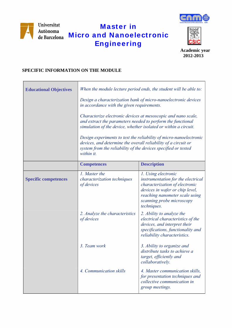
When the module lecture period ends, the student will be able to: Educational Objectives Design a characterization bank of micro-nanoelectronic devices in accordance with the given requirements. Characterize electronic devices at mesoscopic and nano scale, and extract the parameters needed to perform the functional simulation of the device, whether isolated or within a circuit. Design experiments to test the reliability of micro-nanoelectronic devices, and determine the overall reliability of a circuit or system from the reliability of the devices specified or tested within it.
Competences Description
1. Master the characterization techniques of devices
1. Using electronic instrumentation for the electrical characterization of electronic devices in wafer or chip level, reaching nanometer scale using scanning probe microscopy techniques.
Specific competences
2. Analyze the characteristics of devices
2. Ability to analyze the electrical characteristics of the devices, and interpret their specifications, functionality and reliability characteristics.
3. Team work 3. Ability to organize and distribute tasks to achieve a target, efficiently and collaboratively.
4. Communication skills 4. Master communication skills, for presentation techniques and collective communication in group meetings.
Master in Micro and Nanoelectronic
Engineering Academic year
2012-2013
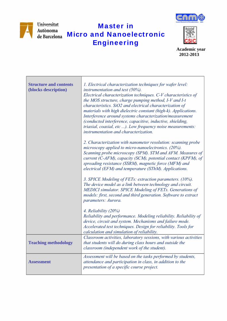
Structure and contents (blocks description)
1. Electrical characterization techniques for wafer level: instrumentation and test (50%). Electrical characterization techniques. C-V characteristics of the MOS structure, charge pumping method, I-V and I-t characteristics. SiO2 and electrical characterization of materials with high dielectric constant (high-k). Applications. Interference around systems characterization/measurement (conducted interference, capacitive, inductive, shielding, triaxial, coaxial, etc ...). Low frequency noise measurements: instrumentation and characterization. 2. Characterization with nanometer resolution: scanning probe microscopy applied to micro-nanoelectronics. (20%). Scanning probe microscopy (SPM). STM and AFM. Measures of current (C-AFM), capacity (SCM), potential contact (KPFM), of spreading resistance (SSRM), magnetic force (MFM) and electrical (EFM) and temperature (SThM). Applications. 3. SPICE Modeling of FETs: extraction parameters. (10%). The device model as a link between technology and circuit. MEDICI simulator. SPICE Modeling of FETs. Generations of models: first, second and third generation. Software to extract parameters: Aurora. 4. Reliability (20%) Reliability and performance. Modeling reliability. Reliability of device, circuit and system. Mechanisms and failure mode. Accelerated test techniques. Design for reliability. Tools for calculation and simulation of reliability.
Classroom activities, laboratory sessions, with various activities
that students will do during class hours and outside the classroom (independent work of the student).
Teaching methodology
Assessment will be based on the tasks performed by students, attendance and participation in class, in addition to the presentation of a specific course project.
Assessment

Master in Micro and Nanoelectronic
Engineering Academic year
2012-2013
References and web links M. L. Green, E. P. Gusev, R. Degraeve, E. L. Garfunkel, “Ultrathin (<4 nm) SiO
2 and Si-O-N gate dielectric layers for
silicon microelectronics: Understanding the processing, structure, and physical and electrical limits”, Journal of Applied Physics, Vol.90, No. 5, pp. 2057-2121. R. Degraeve, B. Kaczer, G. Groeseneken, “Degradation and breakdown in thin oxide layers mechanisms, models and reliability prediction”, Microelectronics Reliability, 39, pp. 1445-1460, 1999. S. Lombardo, J. H. Stathis, B. P. Linder, “Dielectric breakdown mechanisms in gate oxides”, Journal of Applied Physics, 98, p. 121301, 2005. High-k gate dielectrics: Current status and materials properties considerations. G.D. Wilk, R.M. Wallace, J.M. Anthony, J.Appl.Phys. Vol. 86, No. 10, pp. 5243-5275, 2001. P. De Wolf et al, Electrical characterization of semiconductor materials and devices using scanning probe microscopy, Materials Science in Semiconductor Processing, 4(1-3), 71 (2001). B. Ebersberger et al, Application of Scanning Probe Mycroscopy techniques in semiconductor failure analysis, Microelectronics Reliability 41, 1449 (2001). Practical Reliability Engineering,Patrick D. T. O'Connor, John Wiley, 2003 The Assurance Sciences, S. Halpner, Prentice Hall Inc; 2002. Relex Reference Manual; Relex Corporartion, 2002 Failure Analysis Of Integrated Circuits; L.C. Wagner, Kulwer Academic Press, 1999. http://www.veeco.com http://stm2.nrl.navy.mil/how-afm/how-afm.html http://www.chembio.uoguelph.ca/educmat/chm729/afm/firstpag.htm

Master in Micro and Nanoelectronic
Engineering Academic year
2012-2013
GENERAL INFORMATION ON THE MODULE Module Name Embedded Systems
Code 40727 2.2 Course
Timetable ECTS credits 10
Module type Mandatory x Optional
Requirements None
Course Language English Responsible Professor Jordi Carrabina Bordoll
Responsible Department Microelectronics and Electronic Systems
TEACHING TEAM
Professor Department Office e-mail Tutorials timetable
Jordi
Carrabina MiSE QC-2060 [email protected] To be
determined Lluís Terés MiSE (CNM) QC-2060 [email protected] To be
determined
Master in Micro and Nanoelectronic
Engineering Academic year
2012-2013
SPECIFIC INFORMATION ON THE MODULE
When the module lecture period ends, the student will be able to:
Educational Objectives Have an overview of Embedded Systems. Terminology and basic concepts and technologies. Understand the computational requirements, power supply, consumption, interconnection of the different components integrated in embedded systems. Learn the methodologies, tools and technologies for the design of embedded systems, particularly the platform-based design methodologies, the different subsystems, their structure (SoC) and connectivity alternatives (SoC/NoC). Learn how to select and scale the architectural and microarquitectural components of an embedded system, using architectural exploration techniques. Identify the different implementation technologies for embedded systems (homogeneous and heterogeneous MPSoC chips, FPGA, MCM, etc.). Understand and apply the use of tools related to the specification, verification and synthesis of these systems at different levels: system, software application, operating system, middleware, SoC/NoC architecture, and hardware.
Competences Description
1. Specification, analysis and design
1. Specify the environment and research platform itself. Analyze the proposed embedded platforms HW/SW available for different application fields. Analyze function, architecture and performance of the SoC systems. Design applications on embedded platforms restricted in terms of cost, speed, size and consumption.
Specific competences
2. Problem solving 2. Solve problems with a global and critique vision. Understand flexibility in problem solving resulting from the HW/SW codesign, and the architectural synthesis at MPSoC level.
3. Innovation 3. Proposals for specific applications on new platforms for embedded systems design.

Master in Micro and Nanoelectronic
Engineering Academic year
2012-2013
0. Introduction
Presentation of the course. Presentation of students profiles. Set goals for the course, comment content, method and evaluation work. Establish terminology. Bibliography, classical field publications. 1. Introduction to Embedded Systems Embedded systems and real-time operating systems (embedded, real-time, mobile, complex). Platform-based design methodology. Example of heterogeneous platforms. Examples of technologies and applications for embedded systems. 2. SoC Architectures
Structure and contents (blocks description)
Intellectual Property, Integration and virtual components, SoC architectures, VSIA Model and HW/SW Implementation of SoC technologies. NIOS sample. 3. Concepts and Techniques of low energy consumption Energy consumption and abstraction levels. Models and Techniques for low power consumption. Embedded systems management. Memory hierarchy. Example: ULP Microprocessors. 4. Models and Architectures for Complex Electronic Systems Computational models for electronic systems. Heterogeneity and functional-structural polymorphism. Example: MATLAB. Design flow: system architecture, SW, FW, HW, physical. Example: SystemC TLM. Performance and metrics: speed, area and power consumption. Example: design flow from SystemC. Example: SystemC4NIOS. Verification: environments, simulators, formal methods, HIL. Virtualization: PCvirtual. Example: Platform Characterization MHP. MATLAB & HIL: Chain SDR OFDM. NoC architectures and systems. Example: NoCmaker. Parallel computing, distributed and reconfigurable.5. Introduction to Multimedia Systems Multimedia systems structure. DVB. Multimedia applications. Embedded Multimedia Platforms.
Lectures
Seminars by experts and examples Laboratory sessions
Teaching methodology
Design and Implementation of Embedded Systems and SoC
Attendance to lectures, seminars and laboratory (50%). Lab practices in groups (20%). Preparation and presentation of work relating to the course content, extracted from the research work of students (30%).
Assessment

Master in Micro and Nanoelectronic
Engineering Academic year
2012-2013
References and web links Books J.A.Fisher, P. Faraboschi C. Young "Embedded Computing - A VLIW Approach to Architecture, Compilers and Tools." Elsevier 2005. F. Balarin et al. "Hardware-Software Co-Design of Embedded Systems: The POLIS Approach". Kluwe, 1997. Ll. Terés et al. "VHDL: Lenguaje Estándar de Diseño Electrónico" McGraw-Hill, 1998. P. Bricaud, M. Keating: "Reuse Methodology Manual for System-On-A-Chip Designs". Kluwer 1999. Rajsuman Rocha. "System-on-a-Chip: Design and Test." Artech House Pub., 2000. H. Chang et al, "Surviving the SOC Revolution: A Guide to Platform-Based Design", Kluwer Academic Publishers, 1999. J.Duato, S.Yalamanchili, N.Lionel, "Interconnection Networks: An Engineering Approach", Morgan Kaufmann, 2002 F. Cathoor et al. "Custom Memory Management Methodology", Kluwer AP. 1998. F. Catthoor et al, "Data access and storage management for embedded programmable processors", Kluwer AP. 2002. Articles and Links Aarts, E. "Ambient intelligence: a multimedia perspective" IEEE Multimedia. Jan-March 2004. Vol 11, pp: 12 - 19. ISSN: 1070-986X De Man, H. "Ambient intelligence: gigascale dreams and reality Nanoscale" ISSCC 2005. Vol.1 pp. 29-35. ISBN: 0-7803-8904-2A.L.Sangiovanni-Vincentelli. "White paper on Platform-Based Design" & "Principles on Platform-based". http://wwwcad.eecs.berkeley.edu/Respep/Research/asves/embedded/platform_based/platform_based.htm. 2001. L. Cai, D. Gajski, "Transaction Level Modeling: An Overview," Proc. CODES + ISSS 2003. Cmar, R. et al "Platform design approach for re-configurable network appliances." Proc. ICC 2001. . IEEE, p. 79-82

Master in Micro and Nanoelectronic
Engineering Academic year
2012-2013
GENERAL INFORMATION ON THE MODULE
Module Name Nanoelectronic Devices
Code 40598 Course 2.2
Timetable ECTS credits 10
Module type Mandatory x Optional
Requirements None Course Language English Responsible Professor Jordi Suñé Responsible
Department Electronic Engineering TEACHING TEAM
Professor Department Office e-mail Tutorials timetable
Jordi Suñé Electronic Engineering
QC-3041 [email protected] To be determined
David Jiménez
Electronic Engineering
QC-3035 [email protected] To be determined
Xavier Oriols Electronic
Engineering QC-3015 [email protected] To be
determined
Enrique Miranda
Electronic Engineering
QC-3007 [email protected] To be determined

Master in Micro and Nanoelectronic
Engineering Academic year
2012-2013
SPECIFIC INFORMATION ON THE MODULE
When the module lecture period ends, the student will be able to: Educational Objectives - Recognize the major scientific and technological challenges in the development of micro and nano electronics. - Critically interpret and contextualize current research articles related to nanoelectronic devices. - Determine the appropriate level of approximation to the electron transport depending on the considered device. - Be able to develop a basic simulation of electron transport in devices.
Competences Description
1. Problem solving 1. Solve open problems with a global vision and learn to make a critical assessment of the results.
Specific competences
2. Innovation 2. Be able to provide new
innovative ideas in the design of electronic devices.
3. Analysis and design 3. Analysis of devices taking into account their properties with their respective physical and technological parameters in order to design/develop alternatives with optimum performance.

Master in Micro and Nanoelectronic
Engineering Academic year
2012-2013
Structure and contents (blocks description)
Block 1. From microelectronics to nanoelectronics Brief history of the development of microelectronics. State of the art of MOS technology and major future development problems. International Technology Roadmap for Semiconductors. Block 2. Fundamentals of Semiconductor Schrödinger equation. Systems of many electrons. Band structure. Densities of states. Occupation function. Systems of reduced dimensions, two-dimensional electron gas, wires and quantum dots. Block 3. Electronic transport Hierarchy approaches to electron transport devices Semi-classical models. Boltzmann equation. Monte Carlo simulation. Quantum Model, Landauer transmission model. Transport around the effective mass equation. Tunneling effects. Simulation at the atomic scale: semiempirical methods. Block 4. nanoelectronic devices Resonant Tunneling Diode, occasional contacts. MOSFETs nanometric dimensions. Transmission model for nanoscale MOS transistors. Single-electron devices. Transistors with Carbon NanoTubes and Silicon nanowires Spin devices.
The methodology will combine:
a) Classroom activities (20%) - Lectures - Labs - Seminars b) Self-study (outside classroom) (80%) - Analysis of the current challenges of the μ-η-electronics technology based on research papers. Prepare an oral presentation for the class. - Solving proposed problems - Reading articles - Individual study
Teaching methodology
Assessment will be based on:
- Delivery of problems and issues, job analysis and oral presentation (50%). - Final exam (50%).
Assessment

Master in Micro and Nanoelectronic
Engineering Academic year
2012-2013
References and web links M. Lundström. Fundamentals of Carrier Transport (Addison-Wesley, 1990) S. Datta, Electronic transport in mesoscopic systems (Cambridge University Press, 1995) S. Datta. Quantum Transport: Atom to Transistor (Cambridge University Press, 2005).

Master in Micro and Nanoelectronic
Engineering Academic year
2012-2013
GENERAL INFORMATION ON THE MODULE
Module Name Master Thesis
Code 40600 Course 2.2
Timetable ECTS credits 20
Module type x Mandatory Optional
Requirements None Course Language English Responsible Professor David Jiménez Responsible
Department Electronic Engineering TEACHING TEAM
All Ph.D. professors of the Department of Electrical Engineering / Microelectronics and Electronic Systems / Telecommunications and Systems
Engineering

Master in Micro and Nanoelectronic
Engineering Academic year
2012-2013
SPECIFIC INFORMATION ON THE MODULE
Educational Objectives - Develop interest and ability to do research. - Master the specific field techniques. - Be able to find relevant documentary sources in order to advance on the research activities. - Identify new research challenges and know how they can be placed within the context of current research.
Competences Description 1. Problem solving in
research 1. Solve open problems within the own research field.
Specific competences
2. Innovation 2. Be able to provide new innovative ideas in the micro and nanoelectronic field.
3. Communication skills 3. Promote the ability to communicate research advances to the scientific community.

Master in Micro and Nanoelectronic
Engineering Academic year
2012-2013
Structure and contents (blocks description)
- Analysis of the previous research problem. - Search related documentary sources. - Practical work in the laboratory (simulation / experiments). - Subsequent analysis of the problem. - Writing a research report containing the following relevant information: research interest and opportunity within the context of current research, presentation of research methodology, main conclusions of the research, and future research lines on the topic.
Students must perform an independent research work in a
related micro and nanoelectronics area, with mentoring from a Ph.D. professor of the Department of Electrical Engineering / Microelectronics and Electronic Systems / Telecommunication and Engineering Systems
Teaching methodology
The evaluation method consists in an oral presentation of 30 minutes + 20 minutes of discussion in front of a court composed by three Ph.D. members (excluding the mentor) of the Department of Electrical Engineering / Microelectronics and Electronic Systems / Telecommunications and systems Engineering
Assessment
References and web links