
Double-Sided Freeform Lens for Light Collimation of Light ...
13
applied sciences Article Double-Sided Freeform Lens for Light Collimation of Light Emitting Diodes Yong-Sin Syu, Chun-Ying Wu and Yung-Chun Lee * Department of Mechanical Engineering, Cheng Kung University, Tainan 701, Taiwan; [email protected] (Y.-S.S.);[email protected] (C.-Y.W.) * Correspondence: [email protected]; Fax: +886-6-2094-010 Received: 23 October 2019; Accepted: 9 December 2019; Published: 12 December 2019 Abstract: A double-sided freeform lens is proposed for collimating light emitted from light emitting diodes (LEDs). The surface profiles of the lens are mathematically characterized and precisely determined based on a point-source assumption and differential geometry theory. The proposed lens design method is straightforward, flexible, and effective. Moreover, the optical performance of the lens can be intuitively adjusted by tuning just a small number of design parameters. The simulation results showed that the proposed lens achieved an excellent collimating effect for a commercial ultraviolet (UV) LED. A prototype lens is fabricated in UV-grade poly(methyl methacrylate) material using a standard injection molding process. The light collimating effect of the lens/UV-LED assembly was measured experimentally and was shown to be in good agreement with the simulation results. The collimating angle at the half-energy level was equal to 1.88 ◦ . The performance of the UV-LED is thus comparable to that of conventional lithography UV light sources based on mercury arc lamps. Consequently, the proposed double freeform lens showed significant potential for photolithography applications within the industry. Keywords: lenses; light emitting diodes; ultraviolet light; differential geometry; geometrical optics; machining; lithography; collimator surfaces 1. Introduction Compared to the traditional UV mercury lamps used in conventional photolithography systems, ultraviolet (UV) light emitting diodes (LEDs) have the advantage of having a lower cost, a reduced electricity consumption, a longer lifetime, improved stability, and being more environmentally friendly. As a result, there has been growing interest in it being a potential light source for UV lithography processes. However, collimating the UV light without losing too much of the light energy represents a major challenge and requires the use of special lens designs. Both primary and secondary optics are commonly adopted to adjust the distribution of light so as to meet the overall specifications and create the desired beam pattern. Freeform surfaces, in particular, have been widely used to refract and/or reflect LED light. For example, the authors in [1–3] used lenses with a concave spherical surface on the LED side and a freeform refractive surface on the other side to achieve a uniform illumination intensity over a rectangular area. In contrast, the authors in [4–6] used double freeform surfaces to improve the optical performance by refracting the LED light twice. In many cases, the freeform lenses are intimately integrated with the LED packaging in order to achieve compactness [7,8], or better angular color uniformity [9]. For LEDs with a wide radiation angle, more complex freeform surfaces are commonly employed to refract the light at a lower angle and reflect the light at a higher angle [10–17]. The surface profiles in such lenses typically comprise of several discontinuities separating a small number of analog profile sections with different functions. The resulting freeform surfaces are generally designed using numerical schemes and Appl. Sci. 2019, 9, 5452; doi:10.3390/app9245452 www.mdpi.com/journal/applsci
Transcript of Double-Sided Freeform Lens for Light Collimation of Light ...

applied sciences
Article
Double-Sided Freeform Lens for Light Collimation ofLight Emitting Diodes
Yong-Sin Syu, Chun-Ying Wu and Yung-Chun Lee *
Department of Mechanical Engineering, Cheng Kung University, Tainan 701, Taiwan;[email protected] (Y.-S.S.); [email protected] (C.-Y.W.)* Correspondence: [email protected]; Fax: +886-6-2094-010
Received: 23 October 2019; Accepted: 9 December 2019; Published: 12 December 2019�����������������
Abstract: A double-sided freeform lens is proposed for collimating light emitted from light emittingdiodes (LEDs). The surface profiles of the lens are mathematically characterized and preciselydetermined based on a point-source assumption and differential geometry theory. The proposed lensdesign method is straightforward, flexible, and effective. Moreover, the optical performance of thelens can be intuitively adjusted by tuning just a small number of design parameters. The simulationresults showed that the proposed lens achieved an excellent collimating effect for a commercialultraviolet (UV) LED. A prototype lens is fabricated in UV-grade poly(methyl methacrylate) materialusing a standard injection molding process. The light collimating effect of the lens/UV-LED assemblywas measured experimentally and was shown to be in good agreement with the simulation results.The collimating angle at the half-energy level was equal to 1.88◦. The performance of the UV-LED isthus comparable to that of conventional lithography UV light sources based on mercury arc lamps.Consequently, the proposed double freeform lens showed significant potential for photolithographyapplications within the industry.
Keywords: lenses; light emitting diodes; ultraviolet light; differential geometry; geometrical optics;machining; lithography; collimator surfaces
1. Introduction
Compared to the traditional UV mercury lamps used in conventional photolithography systems,ultraviolet (UV) light emitting diodes (LEDs) have the advantage of having a lower cost, a reducedelectricity consumption, a longer lifetime, improved stability, and being more environmentally friendly.As a result, there has been growing interest in it being a potential light source for UV lithographyprocesses. However, collimating the UV light without losing too much of the light energy represents amajor challenge and requires the use of special lens designs.
Both primary and secondary optics are commonly adopted to adjust the distribution of lightso as to meet the overall specifications and create the desired beam pattern. Freeform surfaces, inparticular, have been widely used to refract and/or reflect LED light. For example, the authors in [1–3]used lenses with a concave spherical surface on the LED side and a freeform refractive surface on theother side to achieve a uniform illumination intensity over a rectangular area. In contrast, the authorsin [4–6] used double freeform surfaces to improve the optical performance by refracting the LEDlight twice. In many cases, the freeform lenses are intimately integrated with the LED packagingin order to achieve compactness [7,8], or better angular color uniformity [9]. For LEDs with a wideradiation angle, more complex freeform surfaces are commonly employed to refract the light at alower angle and reflect the light at a higher angle [10–17]. The surface profiles in such lenses typicallycomprise of several discontinuities separating a small number of analog profile sections with differentfunctions. The resulting freeform surfaces are generally designed using numerical schemes and
Appl. Sci. 2019, 9, 5452; doi:10.3390/app9245452 www.mdpi.com/journal/applsci
Appl. Sci. 2019, 9, 5452 2 of 13
computer algorithms. However, Fresnel surfaces have also been proposed for redistributing LED lighton the reflection surface [18,19]. Proposed freeform lens share the same purpose of many other lensdesigns, such as the positive meniscus lens [20], by minimizing the spherical aberration. However,conventional positive meniscus lenses consist of two spherical lens surfaces, and hence their lightcollimating capability is limited only to paraxial rays. In practice, most LEDs have a large radiationangle. Therefore, they cannot be easily collimated to a small collimating angle by a conventionalmeniscus lens without losing the majority of their light energy. Furthermore, most commercial positivemeniscus lenses have a relatively long focal length of around 100 to 1000 mm and are therefore noteasily integrated with LEDs.
The majority of previous studies on the use of freeform surfaces for LEDs consider the problem ofoptical lighting, which generally requires a certain distribution of illumination intensity on a targetarea that is placed quite far from the LED. In such situations, the light collimating effect is not asignificant concern, provided that the light beam has a limited viewing angle in the far field. As aresult, when designing the lens, emphasis is placed mainly on the illumination uniformity and lightefficiency. However, when applying UV-LEDs to photolithography applications, light collimation is amajor concern since it has a direct effect on the dimensional accuracy of the developed photoresist(PR) microstructure. Furthermore, in photolithography, the UV light source is relatively close to thetargeted PR layer, and hence the UV light should be collimated immediately after the freeform lens inthe near field. However, the uniformity of the projected light intensity is less important than in generaloptical lighting applications since the UV patterned area is typically in the wafer size (up to 12”) orpanel size (up to 28”) and hence illumination is generally achieved using an array of lens/LED units inwhich the overlapping exposures of the multiple units are controlled using a programmed scanningmovement [16].
The present study proposes a single lens with two freeform lens surfaces to collimate the lightemitted from an UV-LED. The two surfaces are characterized mathematically as functions in apolar coordinate system. Furthermore, based on fundamental ray optics and differential geometry,the solutions for the two lens surfaces are analytically determined using a point source assumptionand an imaginary point source. One of the freeform lens profiles is solved numerically from a simpleordinary differential equation, while the other has a closed-form solution. The designed doublefreeform lens is evaluated both numerically and experimentally for a real UV-LED. It is shown that thelight beam emitted from the UV-LED is refracted twice by the designed freeform lens’ surface and isincident on the target image plane with a good collimation accuracy.
2. Double Freeform Lens Design for Collimating Light from Point Source
This paper proposes a method for designing a LED light collimating lens with two analog freeformsurfaces. As shown in Figure 1a, the LED light source was first approximated as a point source, S,located at the origin of a (x, z) coordinate system in which the +z-axis is the optical axis of the LED.The lens under consideration was axially symmetrical with respect to the z-axis. Therefore, the x-axiscould be any direction perpendicular to the z-axis. It is noted that a real LED is not a point sourceand its radiation pattern may thus deviate slightly from axial-symmetry. However, after completingthe lens design, a real LED light source was modeled with the designed freeform lens and the overalloptical performance was evaluated. In addition, the designed lens was fabricated and characterizedexperimentally using a commercial UV-LED.
As shown in Figure 1a, the two freeform lens surfaces are denoted as S1 and S2, respectively.The lens was designed such that the light emitted from the point source S was refracted at points P andP′ by surfaces S1 and S2, respectively, and became parallel to the z-axis in air as a result. The opticalrefractive index of the lens material is n. The key element in the proposed freeform lens design methodwas to individually assign surfaces S1 and S2 with different functions such that they perfectly collimatethe light emitted from the point source, S. The function of surface S1 was to refract all rays emitted byS in such a way that they appear to originate from a new imaginary point source S′ (see Figure 1a,b).
Appl. Sci. 2019, 9, 5452 3 of 13
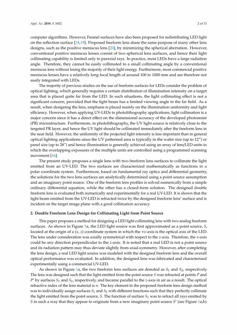
Let ro be the distance between the point source S and the apex point A of surface S1. Note that thelocation of S′ is chosen to be at z = −ξro where ξ is a parameter to be determined. As shown inFigure 1c, the function of surface S2 is to refract all of the rays emitted from point S′ at the lens/airinterface such that they become parallel to the +z axis in air.Appl. Sci. 2020, 10, x FOR PEER REVIEW 3 of 13
Figure 1. Double freeform lens for collimating light from point source: (a) Overview, (b), and (c) details for constructing front (S1) and back (S2) surfaces of lens.
As shown in Figure 1a, the two freeform lens surfaces are denoted as S1 and S2, respectively. The lens was designed such that the light emitted from the point source S was refracted at points P and P’ by surfaces S1 and S2, respectively, and became parallel to the z-axis in air as a result. The optical refractive index of the lens material is n. The key element in the proposed freeform lens design method was to individually assign surfaces S1 and S2 with different functions such that they perfectly collimate the light emitted from the point source, S. The function of surface S1 was to refract all rays emitted by S in such a way that they appear to originate from a new imaginary point source S’ (see Figure 1a,b). Let ro be the distance between the point source S and the apex point A of surface S1. Note
that the location of S’ is chosen to be at oz rξ=− where ξ is a parameter to be determined. As shown in Figure 1c, the function of surface S2 is to refract all of the rays emitted from point S’ at the lens/air interface such that they become parallel to the +z axis in air.
To mathematically derive the equations and solutions for surfaces S1 and S2, the present analysis adopted the polar coordinate systems (r1, θ) and (r2, α) shown in Figure 1b,c, respectively. The
lens design problem then becomes one of finding the functions of 1 1( )r r θ= and 2 2( )r r α= which uniquely characterize and represent surfaces S1 and S2, respectively, and fulfill the refractive functions assigned to them.
As shown in Figure 1b, let n and t
be the normal and tangential unit vectors of surface S1 at an
arbitrary point P, respectively, and let re
and eθ
be the two unit base vectors of polar coordinate
,1( )r θ . Furthermore, let the angle between the incident ray and the normal direction n be denoted
as 1φ . From simple geometry and Snell’s law, it follows that:
1 0 1sin ( cos ) tanr r rθ ξ θ α= + (1)
Figure 1. Double freeform lens for collimating light from point source: (a) Overview, (b), and (c) detailsfor constructing front (S1) and back (S2) surfaces of lens.
To mathematically derive the equations and solutions for surfaces S1 and S2, the present analysisadopted the polar coordinate systems (r1, θ) and (r2, α) shown in Figure 1b,c, respectively. The lensdesign problem then becomes one of finding the functions of r1 = r1(θ) and r2 = r2(α) whichuniquely characterize and represent surfaces S1 and S2, respectively, and fulfill the refractive functionsassigned to them.
As shown in Figure 1b, let→n and
→
t be the normal and tangential unit vectors of surface S1 atan arbitrary point P, respectively, and let
→e r and
→e θ be the two unit base vectors of polar coordinate
(r1, θ). Furthermore, let the angle between the incident ray and the normal direction→n be denoted as
φ1. From simple geometry and Snell’s law, it follows that:
r1 sinθ = (ξr0 + r1 cosθ) tanα (1)
and1 · sinφ1 = n · sin[φ1 − (θ− α)] (2)
Since→r 1 = r1
→e r,
d→r 1
dθ = dr1dθ→e r + r1
→e θ, and
→
t is parallel to d→r 1
dθ , one has
tanφ1 =1r1(dr1/dθ) (3)

Appl. Sci. 2019, 9, 5452 4 of 13
From Equation (2), one can derive:
tanφ1 =sin(θ− α)
cos(θ− α) − (1/n)(4)
Furthermore, from Equation (3), Equations (4) and (1), one has:
dr1
dθ=
[sin(θ− α)
cos(θ− α) − (1/n)
]· r, and α = tan−1
(r1 · sinθ
ξ · ro + r1 cosθ
)(5)
Equation (5) can be viewed as a first order ordinary differential equation (ODE) for functionr1(θ), which mathematically characterized freeform surface S1. Due to its complexity, the ODE cannotbe solved analytically. However, the solution of r1(θ) can be precisely calculated by convertingEquation (5) into an equivalent finite difference equation, i.e.,
r1(θi+1) = r1(θi) +
[sin(θi − αi)
cos(θi − αi) − (1/n)
]· r1(θi) · (θi+1 − θi) i = 0, 1, 2, . . . (6a)
αi = tan−1(
r1(θi) · sinθi
ξ · ro + r1(θi) · cosθi
)i = 0, 1, 2, . . . (6b)
along with a given initial condition:r1(θ = 0
◦
) = ro (6c)
Based on the explicit numerical marching scheme shown in Equation (6a,b), the discrete data ofr1(θ) at different angles can be calculated precisely using a very small angular increment. The calculationof r1(θ), or the surface of S1, can proceed to any arbitrary stopping point B, as shown in Figure 1b.Let θB be the angle of point B with respect to the +z axis when viewed from point source S. In otherwords, θB is the light collecting angle of the designed lens from the point source.
A similar approach can be taken for analyzing surface S2 under the polar coordinate system (r2, α).As shown in Figure 1c, the polar coordinate system was mounted at the imaginary point source S′
with two unit base vectors,→e r and
→e α, respectively.
→n and
→
t again denote the normal and tangentialunit vectors of surface S2 at the refraction point P′, respectively. Furthermore, φ2 denotes the incidentangle. After refraction, the ray should be parallel to the +z axis. Thus, based on simple geometry andSnell’s law, it follows that:
n sinφ2 = 1 · sin(φ2 + α) (7)
ortanφ2 =
sinαn− cosα
. (8)
Since→r 2 = r2
→e r,
d→r 2
dα = dr2dα→e r + r2
→e α, and
→
t is parallel to d→r 2
dα , one has:
tanφ2 = −1r2(dr2/dα) (9)
Furthermore, from Equations (8) and (9) one has:
1r2
dr2 =− sinα
n− cosαdα (10)
Integrating both sides, the analytical solution for r2(α) becomes:
r2(α) = r2∗ ·
(n− cosα∗n− cosα
)(11)

Appl. Sci. 2019, 9, 5452 5 of 13
where (r2∗, α∗) are integration constants and can be the coordinates of any arbitrarily chosen point onthe curved surface S2. One obvious choice is point B, i.e., the ending point of S1 since, by choosingthis point, one can connect profiles S1 and S2 at point B, as shown in Figure 1. Let (r2B, αB) be thecoordinates of point B in the coordinate system (r2, α). The lens profile of S2 can then be analyticallydetermined in the following mathematically closed-form:
r2(α) = r2B ·
(n− cosαB
n− cosα
)(12)
The apex point A′ of surface S2, as indicated in Figure 1, can be determined by setting α = 0, and hence:
r2(0) = r2B ·
(n− cosαB
n− 1
)= ξro + ro + tro (13)
where t represents the total lens thickness (see Figure 1).
3. Lens Design and Simulation with UV-LED
The goal of the present study is to design a collimating lens for UV-LEDs for use in proximity/contactUV photolithography applications, in which highly-collimated UV light is required. Once the UV lightis collimated, a uniform distribution of the UV dosage over the wafer/substrate surface area can beachieved by overlapping the UV exposures of multiple LED/lens units arranged in the form of an arrayusing a pre-programmed mechanical scanning movement.
In the method proposed in Section 2, only three parameters are required to complete the lensdesign, namely ro, ξ, and θB. However, since there is only one characteristic length (ro) involved inthe analysis, ro can be set equal to one such that all of the other dimensions become normalized withrespect to ro. As a result, only two parameters, i.e., ξ and θB, were actually needed for the lens designunder a point-source assumption. In real applications based on the use of true LEDs as the light source,the light is actually emitted from a finite size area with a dimension of d. The larger the ratio of ro to d,the better the point source assumption is, and hence the better the light collimating effect achieved bythe proposed double freeform lens. Regarding the two design parameters, ξ dominates the shape ofthe lens profile and the Fresnel losses, while θB determines the total light collection angle from theLED and therefore governs the energy efficiency of the collimated LED light.
The present study used an NCSU276A UV-LED (Nichia Inc., Tokushima, Japan) for illustrationpurposes. As shown in Table 1, the main features of the UV-LED include a peak wavelength of 365 nm,an optical power of 780 mW, and a radiation angle of 130◦ (full angle at half intensity). The analysiswas performed using commercial Zemax optical design software (OpticStudio, Kirkland, WA, USA).Figure 2a,b show the angular distribution of the illumination intensity of the NCSU276A UV-LED, assimulated using the source model file provided by Nichia Inc. [21]. The results confirmed that the fullangle of divergence measured at half the maximum intensity was indeed around 130◦. Furthermore,the light emitting area size is around 1 × 1 mm2.
Table 1. Main features of NCSU276A UV-LED (Nichia Inc., Tokushima, Japan).
Model No. NCSU276A
Peak Spectrum 365 nmTypical Optical Power 780 mW
Forward Voltage (VF) 3.8 V (Typ.)4.4 V (Max.)
Directivity (2θ, Half Max.) 130◦
Forward Current (IF) 500 mmLED Size 3.5 × 3.5 × 2.0 mm3
Light Emitting Area 1.0 × 1.0 mm2

Appl. Sci. 2019, 9, 5452 6 of 13
Appl. Sci. 2020, 10, x FOR PEER REVIEW 6 of 13
parameters, ξ dominates the shape of the lens profile and the Fresnel losses, while θB determines the total light collection angle from the LED and therefore governs the energy efficiency of the collimated LED light.
The present study used an NCSU276A UV-LED (Nichia Inc., Tokushima, Japan) for illustration purposes. As shown in Table 1, the main features of the UV-LED include a peak wavelength of 365 nm, an optical power of 780 mW, and a radiation angle of 130° (full angle at half intensity). The analysis was performed using commercial Zemax optical design software (OpticStudio, Kirkland, WA, USA). Figure 2a,b show the angular distribution of the illumination intensity of the NCSU276A UV-LED, as simulated using the source model file provided by Nichia Inc. [21]. The results confirmed that the full angle of divergence measured at half the maximum intensity was indeed around 130°. Furthermore, the light emitting area size is around 1 × 1 mm2.
(a)
(b)
Figure 2. Angular distribution of radiation intensity of NCSU276A ultra violet light emitting diode (UV-LED): (a) Rectangular plot and (b) polar plot.
Table 1. Main features of NCSU276A UV-LED (Nichia Inc., Tokushima, Japan).
Model No. NCSU276A Peak Spectrum 365 nm
Typical Optical Power 780 mW
Forward Voltage (VF) 3.8 V (Typ.) 4.4 V (Max.)
Directivity (2θ, Half Max.) 130° Forward Current (IF) 500 mm
LED Size 3.5 × 3.5 × 2.0 mm3 Light Emitting Area 1.0 × 1.0 mm2
The UV-LED collimating lens designed in this study was manufactured using an injection molding technique since it can precisely control the lens surface profiles and enables the mass production of the lens with a high throughput and low cost. The lens was manufactured in PLEXIGLAS® 8012 (Evonik Performance Materials GmbH, Essen, Germany), which is a poly(methyl methacrylate) (PMMA) material suitable for making lenses with a working UV-A spectrum of 365~395 nm and has an optical refraction index (n) of 1.51 – @365 nm [22]. Figure 3a,b show the calculated optical transmission coefficients of the chosen material at the air/lens and lens/air interfaces, respectively, as a function of the incident angle (note that the calculated coefficients are used in the later lens design process). As shown in Figure 3b, the total reflection angle at the PMMA/air interface was around 41°.
Figure 2. Angular distribution of radiation intensity of NCSU276A ultra violet light emitting diode(UV-LED): (a) Rectangular plot and (b) polar plot.
The UV-LED collimating lens designed in this study was manufactured using an injection moldingtechnique since it can precisely control the lens surface profiles and enables the mass production of thelens with a high throughput and low cost. The lens was manufactured in PLEXIGLAS® 8012 (EvonikPerformance Materials GmbH, Essen, Germany), which is a poly(methyl methacrylate) (PMMA)material suitable for making lenses with a working UV-A spectrum of 365~395 nm and has an opticalrefraction index (n) of 1.51 – @365 nm [22]. Figure 3a,b show the calculated optical transmissioncoefficients of the chosen material at the air/lens and lens/air interfaces, respectively, as a functionof the incident angle (note that the calculated coefficients are used in the later lens design process).As shown in Figure 3b, the total reflection angle at the PMMA/air interface was around 41◦.
Appl. Sci. 2020, 10, x FOR PEER REVIEW 7 of 13
(a)
(b)
Figure 3. Fresnel optical transmittance as function of incident angle for: (a) Air to poly(methyl methacrylate) (PMMA) interface, and (b) PMMA to air interface. (Note that the refraction index of the chosen PMMA material is 1.51).
Using the method described in Section 2, several double freeform lenses were designed with ξ-parameter values ranging from 0.1 to 0.9. The calculated S1 and S2 surfaces obtained from Equations (6a,b) and (12) are shown in Figure 4a,b, respectively (note that the refraction index (n) was taken as 1.51 in every case and the collecting angle (θB) was set as 60°). The numerical labels in Figure 4a,b represent the Fresnel transmittance values at the corresponding locations on the boundary surface. It is seen that for the S1 surface, most of the optical transmittance values were around 95% for radiation angles θ = 0°~60° irrespective of the value of ξ . However, for the S2 surface, the optical transmittance at higher radiation angles reduced rapidly (and even reached zero) with increasing ξ due to the effects of internal total reflection. In other words, the flux energy received at larger radiation angles of the LED was completely rejected by the lens.
(a)
Figure 3. Fresnel optical transmittance as function of incident angle for: (a) Air to poly(methylmethacrylate) (PMMA) interface, and (b) PMMA to air interface. (Note that the refraction index of thechosen PMMA material is 1.51).
Using the method described in Section 2, several double freeform lenses were designed withξ-parameter values ranging from 0.1 to 0.9. The calculated S1 and S2 surfaces obtained fromEquations (6a,b) and (12) are shown in Figure 4a,b, respectively (note that the refraction index (n)was taken as 1.51 in every case and the collecting angle (θB) was set as 60◦). The numerical labels inFigure 4a,b represent the Fresnel transmittance values at the corresponding locations on the boundarysurface. It is seen that for the S1 surface, most of the optical transmittance values were around 95%for radiation angles θ = 0◦~60◦ irrespective of the value of ξ. However, for the S2 surface, the opticaltransmittance at higher radiation angles reduced rapidly (and even reached zero) with increasing ξ

Appl. Sci. 2019, 9, 5452 7 of 13
due to the effects of internal total reflection. In other words, the flux energy received at larger radiationangles of the LED was completely rejected by the lens.
Appl. Sci. 2020, 10, x FOR PEER REVIEW 7 of 13
(a)
(b)
Figure 3. Fresnel optical transmittance as function of incident angle for: (a) Air to poly(methyl methacrylate) (PMMA) interface, and (b) PMMA to air interface. (Note that the refraction index of the chosen PMMA material is 1.51).
Using the method described in Section 2, several double freeform lenses were designed with ξ-parameter values ranging from 0.1 to 0.9. The calculated S1 and S2 surfaces obtained from Equations (6a,b) and (12) are shown in Figure 4a,b, respectively (note that the refraction index (n) was taken as 1.51 in every case and the collecting angle (θB) was set as 60°). The numerical labels in Figure 4a,b represent the Fresnel transmittance values at the corresponding locations on the boundary surface. It is seen that for the S1 surface, most of the optical transmittance values were around 95% for radiation angles θ = 0°~60° irrespective of the value of ξ . However, for the S2 surface, the optical transmittance at higher radiation angles reduced rapidly (and even reached zero) with increasing ξ due to the effects of internal total reflection. In other words, the flux energy received at larger radiation angles of the LED was completely rejected by the lens.
(a)
Appl. Sci. 2020, 10, x FOR PEER REVIEW 8 of 13
(b)
Figure 4. Designed lens surface profiles for different values of ξ : (a) Surface S1 and (b) surface S2.
(Note that the numerical labels show the Fresnel transmittance percentages at the corresponding locations).
Based on the angular distribution of the radiation intensity of the chosen NCSU276A UV-LED (see Figure 2a,b) and the Fresnel losses computed at surfaces S1 and S2 (see Figure 4a,b), one can roughly estimate the intensity distribution of the collimated LED beam on a projected plane perpendicular to the z-axis. Figure 5 presents the corresponding results for theξ values considered above. In the present study, the lens profile design calculated for ξ = 0.3 was chosen for illustration purposes since, compared to larger values of ξ , a value of ξ = 3 generally resulted in lower Fresnel losses and limits the lens aperture size and projected area size thereby assuring a higher average projected light intensity. Moreover, a smaller value of ξ (e.g., ξ = 0.1) resulted in a positive slope of surface S2 at point B and hence complicates the computer numerical control (CNC) machining of the steel mold and makes the injection molding of the lens almost impossible.
Figure 5. Double freeform lens designs with different values of ξ (left) and estimated intensity
distribution of collimated beam on projected plane (right).
Figure 4. Designed lens surface profiles for different values of ξ: (a) Surface S1 and (b) surface S2.(Note that the numerical labels show the Fresnel transmittance percentages at the corresponding locations).
Based on the angular distribution of the radiation intensity of the chosen NCSU276A UV-LED (seeFigure 2a,b) and the Fresnel losses computed at surfaces S1 and S2 (see Figure 4a,b), one can roughlyestimate the intensity distribution of the collimated LED beam on a projected plane perpendicularto the z-axis. Figure 5 presents the corresponding results for the ξ values considered above. In thepresent study, the lens profile design calculated for ξ = 0.3 was chosen for illustration purposes since,

Appl. Sci. 2019, 9, 5452 8 of 13
compared to larger values of ξ, a value of ξ = 3 generally resulted in lower Fresnel losses and limits thelens aperture size and projected area size thereby assuring a higher average projected light intensity.Moreover, a smaller value of ξ (e.g., ξ = 0.1) resulted in a positive slope of surface S2 at point B andhence complicates the computer numerical control (CNC) machining of the steel mold and makes theinjection molding of the lens almost impossible.
Appl. Sci. 2020, 10, x FOR PEER REVIEW 8 of 13
(b)
Figure 4. Designed lens surface profiles for different values of ξ : (a) Surface S1 and (b) surface S2.
(Note that the numerical labels show the Fresnel transmittance percentages at the corresponding locations).
Based on the angular distribution of the radiation intensity of the chosen NCSU276A UV-LED (see Figure 2a,b) and the Fresnel losses computed at surfaces S1 and S2 (see Figure 4a,b), one can roughly estimate the intensity distribution of the collimated LED beam on a projected plane perpendicular to the z-axis. Figure 5 presents the corresponding results for theξ values considered above. In the present study, the lens profile design calculated for ξ = 0.3 was chosen for illustration purposes since, compared to larger values of ξ , a value of ξ = 3 generally resulted in lower Fresnel losses and limits the lens aperture size and projected area size thereby assuring a higher average projected light intensity. Moreover, a smaller value of ξ (e.g., ξ = 0.1) resulted in a positive slope of surface S2 at point B and hence complicates the computer numerical control (CNC) machining of the steel mold and makes the injection molding of the lens almost impossible.
Figure 5. Double freeform lens designs with different values of ξ (left) and estimated intensity
distribution of collimated beam on projected plane (right).
Figure 5. Double freeform lens designs with different values of ξ (left) and estimated intensitydistribution of collimated beam on projected plane (right).
The optical performance of the double freeform lens with ξ = 0.3 was evaluated by means ofZemax simulations. The simulations commenced by determining the collimating performance of thelens given the radiation pattern of the NCSU276A UV-LED shown in Figure 2. The simulation resultsshowed that the light emerging from the lens was perfectly collimated with a zero divergent angle.In other words, the accuracy of the proposed collimating lens design under the assumption of a pointsource was confirmed.
The angular distribution of the collimated LED light was then re-simulated using the truefinite-sized model of the NCSU276A LED provided by the manufacturer. In performing the simulations,the LED illuminating chip size was set as 1.0 × 1.0 mm2, while the distance between the LED andlens surface (i.e., ro in Figure 1) was set as 10.65 mm based on a practical consideration of theinjection-molded lens size and the LED intensity level after collimating. Based on the light sourcemodel of the NCSU276A, one million rays were used in the Zemax simulation process together withdesign parameters of ξ = 0.3, θB = 60◦, and ro = 10.65 mm. The angular distribution of the lightintensity was statistically analyzed at a detector plane with a size of 40 × 40 mm2 located at z = +40 mm.Figure 6a shows a two-dimensional view of the ray-tracing results between the finite LED light source,double freeform lens, and detector plane. As shown, not all of the rays collimated and incident on thedetector plane. Thus, while the LED used in the simulations had a total emitting power of 821 mW,the total light power received on the detector plane was just 400.3 mW. In other words, the doublefreeform collimating lens had an energy efficiency of 48.8%, where the losses were due mainly to thecollecting angle of the lens and the Fresnel losses at the air/lens interfaces.
To better understand the light collimating effect of the double freeform lens, for each ray reachingthe detector plane, the collimated angle γ, that is, the angle between the incident ray and the +z axis,was determined, together with the associated light energy of the ray following refraction by lenssurfaces S1 and S2. A statistical analysis was then performed to determine the variation of the total lightintensity with the collimating angle γ. As shown in Figure 6b, around one half (50%) of the collimatedUV-LED light intensity was provided by rays with a collimating angle of less than 1.56◦, while around90% of the intensity was contributed by rays with a collimating angle of less than 3.62◦. Notably, this

Appl. Sci. 2019, 9, 5452 9 of 13
performance was better than that of a conventional mercury lamp and fly’s eye homogenizer system,in which the typical collimating angle is around 1.5◦ at a 50% light intensity level. In other words,the proposed double freeform lens and UV-LED have good potential to replace the mercury lightsources used in conventional lithography applications within the industry.
Appl. Sci. 2020, 10, x FOR PEER REVIEW 9 of 13
The optical performance of the double freeform lens with ξ = 0.3 was evaluated by means of Zemax simulations. The simulations commenced by determining the collimating performance of the lens given the radiation pattern of the NCSU276A UV-LED shown in Figure 2. The simulation results showed that the light emerging from the lens was perfectly collimated with a zero divergent angle. In other words, the accuracy of the proposed collimating lens design under the assumption of a point source was confirmed.
The angular distribution of the collimated LED light was then re-simulated using the true finite-sized model of the NCSU276A LED provided by the manufacturer. In performing the simulations, the LED illuminating chip size was set as 1.0 × 1.0 mm2, while the distance between the LED and lens surface (i.e., ro in Figure 1) was set as 10.65 mm based on a practical consideration of the injection-molded lens size and the LED intensity level after collimating. Based on the light source model of the NCSU276A, one million rays were used in the Zemax simulation process together with design parameters of ξ = 0.3, θB = 60°, and ro = 10.65 mm. The angular distribution of the light intensity was statistically analyzed at a detector plane with a size of 40 × 40 mm2 located at z = +40 mm. Figure 6a shows a two-dimensional view of the ray-tracing results between the finite LED light source, double freeform lens, and detector plane. As shown, not all of the rays collimated and incident on the detector plane. Thus, while the LED used in the simulations had a total emitting power of 821 mW, the total light power received on the detector plane was just 400.3 mW. In other words, the double freeform collimating lens had an energy efficiency of 48.8%, where the losses were due mainly to the collecting angle of the lens and the Fresnel losses at the air/lens interfaces.
(a)
(b)
Figure 6. Zemax simulation results for NCSU276A UV-LED and double freeform lens (ξ = 0.3, θB =
60°and ro = 10.65 mm): (a) 2D view of ray tracing results in Zemax, and (b) percentage of accumulated light intensity within collimating angle (γ).
To better understand the light collimating effect of the double freeform lens, for each ray reaching the detector plane, the collimated angle γ, that is, the angle between the incident ray and the +z axis, was determined, together with the associated light energy of the ray following refraction by lens surfaces S1 and S2. A statistical analysis was then performed to determine the variation of the total light intensity with the collimating angle γ. As shown in Figure 6b, around one half (50%) of the collimated UV-LED light intensity was provided by rays with a collimating angle of less than 1.56°, while around 90% of the intensity was contributed by rays with a collimating angle of less than 3.62°. Notably, this performance was better than that of a conventional mercury lamp and fly’s eye homogenizer system, in which the typical collimating angle is around 1.5° at a 50% light intensity level. In other words, the proposed double freeform lens and UV-LED have good potential to replace the mercury light sources used in conventional lithography applications within the industry.
Figure 6. Zemax simulation results for NCSU276A UV-LED and double freeform lens (ξ = 0.3,θB = 60◦and ro = 10.65 mm): (a) 2D view of ray tracing results in Zemax, and (b) percentage ofaccumulated light intensity within collimating angle (γ).
4. Experiment Results
As described in the previous section, the designed double freeform lens was manufacturedby injection molding in UV-grade PMMA polymer PLEXIGLAS® 8012 (Evonik Industries, Essen,Germany). A two-piece steel mold was first fabricated by a CNC machining system in accordance withthe designed lens profile shown in Figure 5 for ξ = 0.3, θB = 60◦, and ro = 10.65 mm. The dividing pointbetween the profiles of the two injection molds was set as point B. Mass-production of the PMMA lenswas then carried out using a standard injection molding system. Figure 7 shows a photograph of thedouble freeform lens produced in a typical molding cycle.
Appl. Sci. 2020, 10, x FOR PEER REVIEW 10 of 13
4. Experiment Results
As described in the previous section, the designed double freeform lens was manufactured by injection molding in UV-grade PMMA polymer PLEXIGLAS® 8012 (Evonik Industries, Essen ,Germany). A two-piece steel mold was first fabricated by a CNC machining system in accordance with the designed lens profile shown in Figure 5 for ξ = 0.3, θB = 60°, and ro = 10.65 mm. The dividing point between the profiles of the two injection molds was set as point B. Mass-production of the PMMA lens was then carried out using a standard injection molding system. Figure 7 shows a photograph of the double freeform lens produced in a typical molding cycle.
(a)
(b)
(c)
Figure 7. Photograph of double freeform lens produced by injection molding of UV-graded PMMA polymer. (a) Side view; (b) Front view; (c) Close side view
Figure 8 presents a schematic illustration of the experimental setup used to measure the optical performance of the fabricated lens with the NCSU276A UV-LED illumination source. As shown, the system consisted mainly of the collimating lens and UV-LED with correct distance and positioning between them, a CCD camera (FLIR Systems Inc., CM3-U3-13S2M-CS, Wilsonville, OR, USA), and a pin-hole plate. The pin-hole had a diameter of 50 µm and was placed at a distance of 4 mm from the sensing pixels of the CCD. Moreover, the assembled pin-hole/CCD unit was mounted such that it faced the lens/LED along its optical axis (z-axis). Consequently, following the lens collimation, the LED light passed through the pin-hole and was incident on the sensing pixels of the CCD. The intensity and distribution of the light incident on the pixel surface were determined using a calibration process with an optical power meter. Briefly, the distribution of the light intensity with respect to the incident angle was obtained using a simple geometry relationship between each sensing pixel and the pin-hole, while the overall light intensity and its distribution as a function of the collimating angle was determined by scanning the pin-hole/CCD or lens/LED along both x- and y- directions. The LED used in the experiment had a total emitting power of 348.5 mW under drive current of 500 mA, and the total light power received on the detector plane was just 152.6 mW. In other words, the double freeform collimating lens had an energy efficiency of 43.79%. Figure 8b shows the results obtained for the accumulated light intensity within a collimating angle of γ. It is seen that around one half (50%) of the collimated UV-LED light intensity was obtained within a collimating angle of less than 1.88°, while 90% of the intensity was obtained within a collimating angle of less than 4.84°. In other words, the experimental results are in good qualitative agreement with the simulation results shown in Figure 6b. The discrepancy between the two sets of results arose most likely from machining errors of the lens profiles, experimental misalignments between the lens and the LED, and slight variations in the lens material constants. Nevertheless, the overall performance of the proposed lens in collimating the LED light was confirmed.
Figure 7. Photograph of double freeform lens produced by injection molding of UV-graded PMMApolymer. (a) Side view; (b) Front view; (c) Close side view
Figure 8 presents a schematic illustration of the experimental setup used to measure the opticalperformance of the fabricated lens with the NCSU276A UV-LED illumination source. As shown,the system consisted mainly of the collimating lens and UV-LED with correct distance and positioningbetween them, a CCD camera (FLIR Systems Inc., CM3-U3-13S2M-CS, Wilsonville, OR, USA), and a

Appl. Sci. 2019, 9, 5452 10 of 13
pin-hole plate. The pin-hole had a diameter of 50 µm and was placed at a distance of 4 mm from thesensing pixels of the CCD. Moreover, the assembled pin-hole/CCD unit was mounted such that it facedthe lens/LED along its optical axis (z-axis). Consequently, following the lens collimation, the LED lightpassed through the pin-hole and was incident on the sensing pixels of the CCD. The intensity anddistribution of the light incident on the pixel surface were determined using a calibration process withan optical power meter. Briefly, the distribution of the light intensity with respect to the incident anglewas obtained using a simple geometry relationship between each sensing pixel and the pin-hole, whilethe overall light intensity and its distribution as a function of the collimating angle was determinedby scanning the pin-hole/CCD or lens/LED along both x- and y- directions. The LED used in theexperiment had a total emitting power of 348.5 mW under drive current of 500 mA, and the totallight power received on the detector plane was just 152.6 mW. In other words, the double freeformcollimating lens had an energy efficiency of 43.79%. Figure 8b shows the results obtained for theaccumulated light intensity within a collimating angle of γ. It is seen that around one half (50%)of the collimated UV-LED light intensity was obtained within a collimating angle of less than 1.88◦,while 90% of the intensity was obtained within a collimating angle of less than 4.84◦. In other words,the experimental results are in good qualitative agreement with the simulation results shown inFigure 6b. The discrepancy between the two sets of results arose most likely from machining errors ofthe lens profiles, experimental misalignments between the lens and the LED, and slight variations inthe lens material constants. Nevertheless, the overall performance of the proposed lens in collimatingthe LED light was confirmed.
Appl. Sci. 2020, 10, x FOR PEER REVIEW 11 of 13
(a) (b)
Figure 8. Experimental measurement results for double freeform collimating lens with NCSU276A UV-LED: (a) Schematic illustration of experimental setup, and (b) measured total light intensity within collimating angle (γ).
When applying UV-LEDs to conventional proximity/contact photolithography, two of the most important requirements include a small collimating angle and a uniform distribution of the UV light intensity over a large area. The results presented in Figure 8 confirm the ability of the proposed double freeform lens to collimate the UV light from a UV-LED with a small collimating angle. In other words, the proposed lens satisfied the first requirement. However, to meet the second requirement, it is necessary to utilize an array of LED/lens units and an oblique scanning method. For example, as shown schematically in Figure 9a, a tilted array of LED/lens units were deployed at an angle with respect to the nominated scanning direction (e.g., the y-axis) and the arrayed UV light sources are then scanned together across the surface of the photoresist-coated substrate at a constant speed. Each LED/lens unit in the array draws its own scanning line, and the aim is thus to equally space all of the scanning lines such that the UV light energy is evenly distributed in both the x- and the y-directions. As shown in Figure 9a, such an approach results in an effective exposure area in the central area of the array within which the accumulated UV light intensity is uniform and can hence be applied for photolithography. The proposed double freeform lens had an aperture diameter of 24.5 mm. Hence, the center-to-center distance in the 6 × 6 array was chosen as 25.4 mm (see Figure 9a) such that the assembly of the arrayed LED/lens units was mechanically feasible. Figure 9b shows the simulation results obtained for the accumulated UV intensity after scanning by the array (note that the results are based on the simulated radiation intensity pattern for each LED/lens unit given in Figure 5.) The results confirm that a uniform intensity distribution was obtained within the effective exposure area. It is noted that in real applications, the intensity uniformity is inevitably degraded by the variation and positional accuracy of the UV-LEDs and lenses in the array. However, the simulation results presented in Figure 9b nevertheless confirmed the general feasibility of applying LED/lens units for large-area photolithography.
Figure 8. Experimental measurement results for double freeform collimating lens with NCSU276AUV-LED: (a) Schematic illustration of experimental setup, and (b) measured total light intensity withincollimating angle (γ).
When applying UV-LEDs to conventional proximity/contact photolithography, two of the mostimportant requirements include a small collimating angle and a uniform distribution of the UV lightintensity over a large area. The results presented in Figure 8 confirm the ability of the proposeddouble freeform lens to collimate the UV light from a UV-LED with a small collimating angle. In otherwords, the proposed lens satisfied the first requirement. However, to meet the second requirement,it is necessary to utilize an array of LED/lens units and an oblique scanning method. For example,

Appl. Sci. 2019, 9, 5452 11 of 13
as shown schematically in Figure 9a, a tilted array of LED/lens units were deployed at an anglewith respect to the nominated scanning direction (e.g., the y-axis) and the arrayed UV light sourcesare then scanned together across the surface of the photoresist-coated substrate at a constant speed.Each LED/lens unit in the array draws its own scanning line, and the aim is thus to equally spaceall of the scanning lines such that the UV light energy is evenly distributed in both the x- and they-directions. As shown in Figure 9a, such an approach results in an effective exposure area in thecentral area of the array within which the accumulated UV light intensity is uniform and can hencebe applied for photolithography. The proposed double freeform lens had an aperture diameter of24.5 mm. Hence, the center-to-center distance in the 6 × 6 array was chosen as 25.4 mm (see Figure 9a)such that the assembly of the arrayed LED/lens units was mechanically feasible. Figure 9b showsthe simulation results obtained for the accumulated UV intensity after scanning by the array (notethat the results are based on the simulated radiation intensity pattern for each LED/lens unit given inFigure 5). The results confirm that a uniform intensity distribution was obtained within the effectiveexposure area. It is noted that in real applications, the intensity uniformity is inevitably degraded bythe variation and positional accuracy of the UV-LEDs and lenses in the array. However, the simulationresults presented in Figure 9b nevertheless confirmed the general feasibility of applying LED/lens unitsfor large-area photolithography.Appl. Sci. 2020, 10, x FOR PEER REVIEW 12 of 13
Figure 9. (a) Illustrative example of UV-LED/lens unit array for oblique photolithography scanning, and (b) simulated UV intensity distribution and its uniformity over effective exposure area.
5. Conclusions
This paper presented a double-sided freeform lens for collimating light emitted from a LED. In developing the proposed lens, the analyses assumed a point light source, and the continuous lens profiles were characterized mathematically by polar coordinates. It was shown that the two surface profiles of the lens could be analytically represented and determined using an ordinary differential equation and a closed-form solution, respectively. Notably, the overall performance of the lens/LED unit could be adjusted by tuning just two design parameters. As a result, the proposed double freeform lens provided a more attractive and feasible solution for collimating light produced by commercial UV-LEDs.
The optical performance of the proposed double freeform lens was simulated for a commercial UV-LED with a finite light emitting area of approximately 1 × 1 mm2 and a full radiation angle of 130°. The simulation results showed that the lens had a power efficiency of approximately 48.8% and the power efficiency of experiment’s result was 43.79%. In addition, the collimating angles for 50% and 90% of the total light intensity were 1.56° and 3.62°, respectively. A prototype lens was fabricated in UV-grade PMMA polymer using a standard injection molding technique. The optical performance of the lens/LED was characterized experimentally. It was shown that for a lens aperture diameter of 24.5 mm with a central distance of 10.65 mm between the lens and the LED, and an opening aperture angle of ±60°, the collimating angles for 50% and 90% of the total light intensity were 1.88° and 4.84°, respectively. The results therefore confirmed the potential for applying the proposed double freeform lens and UV-LED not only to photolithography, but also to other applications, such as a printed circuit board and integrated circuit package.
Author Contributions: Conceptualization, Y.-C.L.; Data curation, Y.-S.S.; Formal analysis, C.-Y.W.; Methodology, Y.-C.L.; Project administration, Y.-C.L.; Resources, C.-Y.W.; Software, Y.-S.S. and C.-Y.W.; Supervision, Y.-C.L.; Validation, Y.-S.S.; Visualization, C.-Y.W.; Writing—Original draft, Y.-S.S.
Funding: This research was funded by the Southern Taiwan Science Park Bureau and Ministry of Science and Technology of Taiwan under Project Nos. 106GF08, MOST 106-3114-8-006-003 and MOST 107-2823-8-006-004.
Figure 9. (a) Illustrative example of UV-LED/lens unit array for oblique photolithography scanning,and (b) simulated UV intensity distribution and its uniformity over effective exposure area.
5. Conclusions
This paper presented a double-sided freeform lens for collimating light emitted from a LED.In developing the proposed lens, the analyses assumed a point light source, and the continuous lensprofiles were characterized mathematically by polar coordinates. It was shown that the two surfaceprofiles of the lens could be analytically represented and determined using an ordinary differentialequation and a closed-form solution, respectively. Notably, the overall performance of the lens/LEDunit could be adjusted by tuning just two design parameters. As a result, the proposed double
Appl. Sci. 2019, 9, 5452 12 of 13
freeform lens provided a more attractive and feasible solution for collimating light produced bycommercial UV-LEDs.
The optical performance of the proposed double freeform lens was simulated for a commercialUV-LED with a finite light emitting area of approximately 1 × 1 mm2 and a full radiation angle of 130◦.The simulation results showed that the lens had a power efficiency of approximately 48.8% and thepower efficiency of experiment’s result was 43.79%. In addition, the collimating angles for 50% and90% of the total light intensity were 1.56◦ and 3.62◦, respectively. A prototype lens was fabricated inUV-grade PMMA polymer using a standard injection molding technique. The optical performanceof the lens/LED was characterized experimentally. It was shown that for a lens aperture diameter of24.5 mm with a central distance of 10.65 mm between the lens and the LED, and an opening apertureangle of ±60◦, the collimating angles for 50% and 90% of the total light intensity were 1.88◦ and 4.84◦,respectively. The results therefore confirmed the potential for applying the proposed double freeformlens and UV-LED not only to photolithography, but also to other applications, such as a printed circuitboard and integrated circuit package.
Author Contributions: Conceptualization, Y.-C.L.; Data curation, Y.-S.S.; Formal analysis, C.-Y.W.; Methodology,Y.-C.L.; Project administration, Y.-C.L.; Resources, C.-Y.W.; Software, Y.-S.S. and C.-Y.W.; Supervision, Y.-C.L.;Validation, Y.-S.S.; Visualization, C.-Y.W.; Writing—Original draft, Y.-S.S.
Funding: This research was funded by the Southern Taiwan Science Park Bureau and Ministry of Science andTechnology of Taiwan under Project Nos. 106GF08, MOST 106-3114-8-006-003 and MOST 107-2823-8-006-004.
Acknowledgments: The authors are grateful for the technical and equipment support provided by the Center forMicro/Nano Science and Technology at National Cheng Kung University (Taiwan).
Conflicts of Interest: The authors declare no conflict of interest.
References
1. Ding, Y.; Liu, X.; Zheng, Z.-R.; Gu, P.-F. Freeform LED lens for uniform illumination. Opt. Express 2008, 16,12958–12966. [CrossRef] [PubMed]
2. Luo, Y.; Feng, Z.; Han, Y.; Li, H. Design of compact and smooth free-form optical system with uniform.illuminance for LED source. Opt. Express 2010, 18, 9055–9063. [CrossRef] [PubMed]
3. Zhao, Z.; Zhang, H.; Zheng, H.; Liu, S. New reversing freeform lens design method for led uniformillumination with extended source and near field. Opt. Commun. 2018, 410, 123–129. [CrossRef]
4. Hu, R.; Gan, Z.; Luo, X.; Zheng, H.; Liu, S. Design of double freeform-surface lens for LED uniformillumination with minimum Fresnel losses. Optik 2013, 124, 3895–3897. [CrossRef]
5. Wu, H.; Zhang, X.; Ge, P. Double freeform surfaces lens design for LED uniform illumination with highdistance-height ratio. Opt. Laser Technol. 2015, 73, 166–172. [CrossRef]
6. Wu, R.; Huang, C.Y.; Zhu, X.; Cheng, H.; Liang, R. Direct three-dimensional design of compact andultraefficient freeform lenses for extended light sources. Optica 2016, 3, 840–843. [CrossRef]
7. Wang, K.; Chen, F.; Liu, Z.Y.; Luo, X.B.; Liu, S. Design of compact freeform lens for application specific.Light-Emitting Diode packaging. Opt. Express 2010, 18, 413–425. [CrossRef] [PubMed]
8. Wang, S.; Wang, K.; Chen, F.; Liu, S. Design of primary optics for LED chip array in road lighting. Application.Opt. Express 2011, 19 (Suppl. S4), A716–A724. [CrossRef]
9. Hu, R.; Luo, X.; Zheng, H.; Zong, Q.; Gan, Z.; Wu, B.; Liu, S. Design of a novel freeform lens for LED uniformillumination and conformal phosphor coating. Opt. Express 2012, 20, 13727–13737. [CrossRef] [PubMed]
10. Zhenrong, Z.; Xiang, H.; Xu, L. Freeform surface lens for LED uniform illumination. Appl. Opt. 2009, 48,6627–6634. [CrossRef] [PubMed]
11. Zhao, S.; Wang, K.; Chen, F.; Wu, D.; Liu, S. Lens design of LED searchlight of high brightness and distantspot. J. Opt. Soc. Am. A 2011, 28, 815–820. [CrossRef] [PubMed]
12. Chen, J.; Wang, T.; Huang, K.; Liu, T.; Tsai, M.; Lin, C. Freeform lens design for LED collimating illumination.Opt. Express 2012, 20, 10984–10995. [CrossRef] [PubMed]
13. Tsai, C.-Y. Design and analysis of reflector for uniform light-emitting diode illuminance. J. Opt. Soc. Am. A2013, 30, 993–1001. [CrossRef] [PubMed]
Appl. Sci. 2019, 9, 5452 13 of 13
14. Chen, Y.; Wu, S.W.Y.; Ren, Y.; Guan, W.; Zhou, Y. Long-range visible light communication system based onLED collimating lens. Opt. Commun. 2016, 377, 83–88. [CrossRef]
15. Pan, C.-T.; Yang, T.-L.; Chen, Y.-C.; Chang, C.-M.; Hsu, J.-H.; Huang, J.-C. Design of freeform lens with TFMGreflector for UV-LEDs lithography system. Optik 2016, 127, 6850–6857. [CrossRef]
16. Kuo, S.-H.; Chen, C.-F. Design of a collimated UV-LED exposure unit based on light spread function method.Appl. Opt. 2017, 56, 5542–5549. [CrossRef] [PubMed]
17. Luo, T.; Wang, G. Compact collimators designed with a modified point approximation for light emittingdiodes. Proc. SPIE 2017, 10379, 103790G.
18. Hui, X.; Liu, J.; Wan, Y.; Lin, H. Realization of uniform and collimated light distribution in a singlefreeform-Fresnel double surface LED lens. Appl. Opt. 2017, 56, 4561–4565. [CrossRef] [PubMed]
19. Zhao, Z.; Zhang, H.; Liu, S.; Wang, X. Effective freeform TIR lens designed for LEDs with high angular coloruniformity. Appl. Opt. 2018, 57, 4216–4221. [CrossRef] [PubMed]
20. N-BK7 Positive Meniscus Lenses, (Thorlabs, Inc., United States). Available online: https://www.thorlabs.com/newgrouppage9.cfm?objectgroup_id=130 (accessed on 23 October 2019).
21. Source Model File for Zemax Software Nichia Inc. NCSU276A UV-LED. Available online: https://www.nichia.co.jp/specification/products/led/NCSU276A-E.pdf (accessed on 23 October 2019).
22. PLEXIGLAS®8012 Material Manual, (Evonik Performance Materials GmbH, Essen, Germany). Availableonline: https://corporate.evonik.com/en/ (accessed on 23 October 2019).
© 2019 by the authors. Licensee MDPI, Basel, Switzerland. This article is an open accessarticle distributed under the terms and conditions of the Creative Commons Attribution(CC BY) license (http://creativecommons.org/licenses/by/4.0/).