DOPPLER TARGET SIGNAL GENERATOR - apps.dtic.milcoherent pulse doppler radar which makes full use of...
42
0 National Dtfense U ~ Detence nationale DOPPLER TARGET SIGNAL GENERATOR by K. Doucet and J. Nielson Radar Countermeasures Section Electronic Warfare Division ITI DEFENCE RESEARCH ESTABLISHMENT OTTAWA TECHNICAL NOTE 88-14 PCN April 1988 041LD1 1 apr Ottawa
Transcript of DOPPLER TARGET SIGNAL GENERATOR - apps.dtic.milcoherent pulse doppler radar which makes full use of...

0 National DtfenseU ~ Detence nationale
DOPPLER TARGET SIGNAL GENERATOR
by
K. Doucet and J. NielsonRadar Countermeasures Section
Electronic Warfare Division
ITI
DEFENCE RESEARCH ESTABLISHMENT OTTAWATECHNICAL NOTE 88-14
PCN April 1988041LD1 1 apr Ottawa

ABSTRACT
The Threat Radar Simulator (TRS), utilized in DREO's ECM facility, isequipped with a Moving Target Indicator (MTI) processor used to detect theskin echo of moving targets. The MTI unit makes use of a doppler shift,associated with the moving target, to discriminate between the target andunwanted clutter. To facilitate the MTI's requirement for doppler shifts inthe return pulses, a Doppler Target Signal Generator (DTSG) has been developedat DREO. The DTSG is an X-band programmable frequency synthesizer with threeindependent outputs. Two of the outputs are used in the generation of targetreturns and the third outrut provides a doppler shift to the clutter returnsignal.
RESUME
Le simulateur de menace radar utilis6 dans le systime de contremesures6lectroniques du CRDO comprend un indicateur de cibles mobiles pour lad~tection d'6chos d'objets en mouvements. L'indicateur de cibles mobilesutilise l'effet Doppler des 6chos pour s~parer les r~flexions utiles desautres. Un g~n6rateur d'ichos Doppler pour signaux a 6t6 d~velopp6 au CRDOafin de produire des d~placements Doppler d'6chos pour les besoins de ..l'indicateur de cibles mobiles. Le g6n~rateur d'6chos Doppler est constitu6 .d'un synth~tiseur de fr~quences operant dans la bande X et produisant 3sorties ind~pendantes. Deux des sorties sont utilis~s pour la g~n~rationd'echos de cibles et la troisi me produit le d~placement Doppler de l'echod' interference.
.PIN,
OTICT
J i -
A.. L4. )PdJ1.
Dlst J ,.;i l rp

TABLE OF CONTENTS ... ePage
ABSTRACT/RESUME ............ ... .......................... iii
TABLE OF CONTENTS .......... ............................. v
LIST OF FIGURES ........... .......................... ... vii
1.0 INTRODUCTION .......... ............................. .
2.0 DESIGN CONSIDERATIONS FOR THE DTSG ................... . .. 1
2.1 Theory of Doppler Frequency .......... .................. 12.2 EWESF Target Signal Generator Implementation ...... .......... 8
3.0 DTSG RF Design ......... ......................... ... 15
3.1 Introduction .......... .......................... ... 153.2 Loop Filter Used in PLL ...... .................... ... 15
3.2.1 General ........... ............................ ... 15 83.2.2 Search Mode .......... .......................... ... 193.2.3 Lock Mode .......... ........................... ... 22 -
3.3 Performance of Microwave PLL ..... .................. ... 233.4 VCXO Frequency Stabilization ..... .................. ... 283.5 Doppler Frequency Monitor ...... ................... ... 28
4.0 DTSG CONTROL SECTION ....... ...................... ... 33
5.0 CONCLUSION .......... ........................... .... 35
6.0 REFERENCES ............ ........................... 35
".
v'
%,
LIST OF FIGURES
PAGE
FIGURE 1-1: Block Diagram of the Electronic WarfareEngagement Simulation Facility ...... ............. 2
FIGURE 2-1: Phase Front Radiating From a Point Source .... ........ 4
FIGURE 2-2: Phase Front Radiated From a Two-Element Target .. ..... 4
FIGURE 2-3: Illustration of Angle Scintillation ..... ........... 5
FIGURE 2-4: Probability Density Distribution of a 707 Jet ... ...... 7
FIGURE 2-5: Doppler Frequency Spectrum of a PropellerDriven Aircraft .......... ..................... 9
FIGURE 2-6: Doppler Spectrum of an Approaching Single-EngineTurbojet Fighter Aircraft ........ ................ 9
FIGURE 2-7: Target Signal Generation ........ ................ 10
FIGURE 2-8: Block Diagram of DTSG ...... .................. . I. 11
FIGURE 2-9: Coherent Form of Target Signal Generation ......... ... 13
FIGURE 2-10: Output Spectra of SSB Modulator ... ............. ... 14
FIGURE 2-11: Approach Using a Microwave PLL ... ............. ... 16
FIGURE 3-1: RF Portion of Doppler Target Signal Generator ... ...... 17
FIGURE 3-2: Block Diagram of Loop Filter ... .............. ... 18
FIGURE 3-3: Circuitry Used For Lock Detection ... ............ ... 20
FIGURE 3-4: Timing Diagram of Lock Up ..... ................ ... 21
FIGURE 3-5: Frequency Response of 3rd Order Butterworth LPF ....... 24
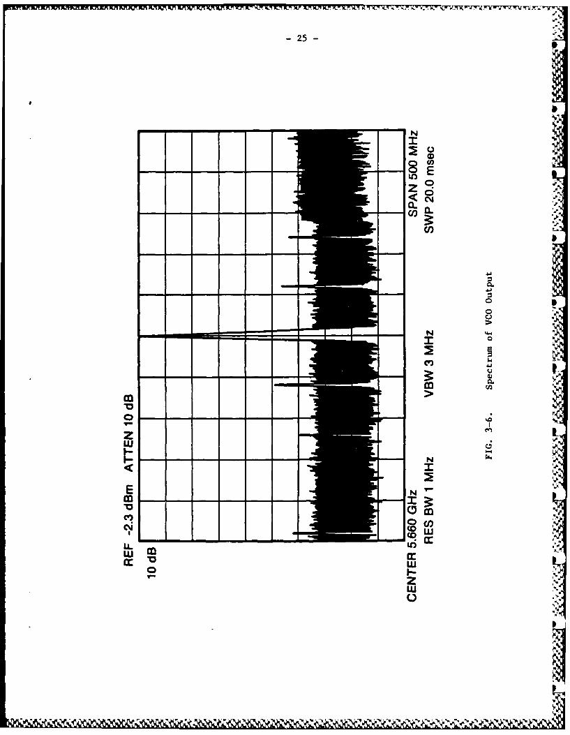
FIGURE 3-6: Spectrum of VCO Output ..... ................. ... 25
FIGURE 3-7: Comparing the output spectrum of the DTSG with anHP8672A synthesizer set at 9.06 GHz ............. ... 26
FIGURE 3-8: Output Spectra of DTSG with and without doppler ........ 27
vii

LIST OF FIGURES (cont)
PAGE
FIGURE 3-9: VCXO Frequency Stabilization ..... .............. ... 294a
FIGURE 3-10: Circuitry for Determining Sign Bit of theDoppler Frequency fd ...... ................. .. 30
FIGURE 3-11: Multiplexing VCXO Outputs into Frequency Counter . . . . 32
FIGURE 3-12: Block Diagram of Frequency Counter ............... .
ix..
V

1.0 INTRODUCTION
The Electronic Wafare Engagement Simulation Facility (EWESF) at DREO iscomprised of an RF anechoic chamber, a Threat Radar Simulator (TRS), aTarget/Jammer/Clutter (TJC) signal generator and an ECM Simulator computer.The inter modular connections are illustrated in Figure 1-1. Target returnand jamming signals are generated from the TJC signal generator andtransmitted through a dipole antenna array network located at one end of thechamber. The radiated signals are received at the opposite end by the radar'santenna, which processes the signals to produce range tracking, antennasteering, and display information. The TRS system is a noncoherent 2 channelmonopulse radar equipped with various signal processing modules including aMoving Target Indicator (MTI). The MTI is a noise suppressing device used tohelp the radar distinguish moving targets from unwanted stationary objects orclutter. The MTI circuit consists of a digital high pass filter designed toaccept doppler frequency shifts associated with moving targets and reject lowor no doppler frequency shifts produced by clutter.
To facilitate the MTI's requirement for a doppler shifted signal, aDoppler Target Signal Generator (DTSG) was developed and implemented into theEWESF. The DTSG is a programmable frequency synthesizer with threeindependent outputs, two of which provide doppler shifts to individual targetreturn signals and one which provides a doppler shift to the clutter signal.The DTSG obtains and processes, from the ECM simulator computer, theinstantaneous velocity of a target relative to the radar's platform, tocalculate the appropriate doppler frequency. The DTSG can produce positiveand negative doppler frequency shifts to represent a target travelling towardsor away from the radar respectively.
In addition to a doppler shift, the DTSG can produce frequency sidebandsto simulate the complete spectral profile of a complex target. This featureis presently not required since the non-coherent MTI processor in the radar isinsensitive to such narrow sidebands. This feature however will accommodate acoherent pulse doppler radar which makes full use of the target's dopplersidebands to discriminate against clutter returns.
The next section includes a theoretical discussion of the dopplerfrequency phenomenon. Mathematical equations which describe the dopplereffect are brought to light to serve as the basis for the design of the DTSG.Also, a description of the EWESF's Target Signal Generator is provided withemphasis given on the DTSG's implementation. Finally, sections 3 and 4provide an overview of the RF and digital designs of the DTSG respectively.
2.0 DESIGN CONSIDERATIONS FOR THE DTSG
2.1 Theory of Doppler Frequency
Targets are generally much larger than the carrier wavelength of theradar pulse and are usually of irregular shape. This combination causes thephase and amplitude of the echo to be a sensitive function of the carrierfrequency and target orientation with respect to the radar boresight axis.Consequently, the phase and amplitude of the echo from a moving target arerandom processes in time. A brief discussion on these processes for the pulseradar, with and without frequency agility, is given. This provides thebackground for describing the hardware implementation of the Doppler TargetSignal Generator (DTSG).

i
RADARSIMULATOR COMPUTER]
2 ,III
AN ECHO IC .
CHAMBER
CONTROL
TARGET EMDISPLAYJM R SIMULATOR
CAMBER a,~'
C TRCOMPUTER TERMINAL
FIG. 1-I. Block Diagram of the Electronic Warfare Engagement SimulationFacility
-.
~:?W~fi*.-?. ~ P
' T - * h . ; %.' *. .= i > ,.:,.,,...,.. .,_., .... . .... . . -. . ., ,.... - .. . .... ... ;.

3-
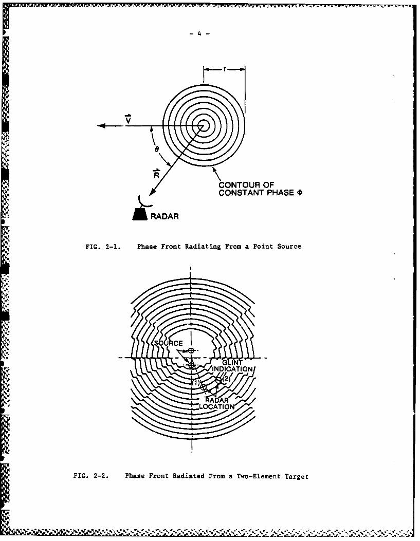
The phase front of a point source excited by a CW radar is shown inFigure 2-1. The total angular displacement of the electromagnetic wave to andfrom the target is given by:
(b = 4__r (2-1)
where -
= RF carrier wavelengthr = radial distance from point source target to phase contour. 0
For a fixed distance r, the phase contours are concentric circles,exhibiting no amplitude fluctuation (scintillation) or angle variation (glint)for any radar viewing angle e. Thus the only requirement for simulating thistarget (assuming that it is in motion) is the doppler frequency which can beexpressed as:
fd 1 db (2-2)21 dt
From Eq. 2-1 and Eq. 2-2 e".
fd= 4ir dR =2 vcos e (2-3)21rX dt X
where
R= position vector between the radar and point sourcev = target velocity 3e = angle between R and direction of
target propagation (see Figure 2-1)
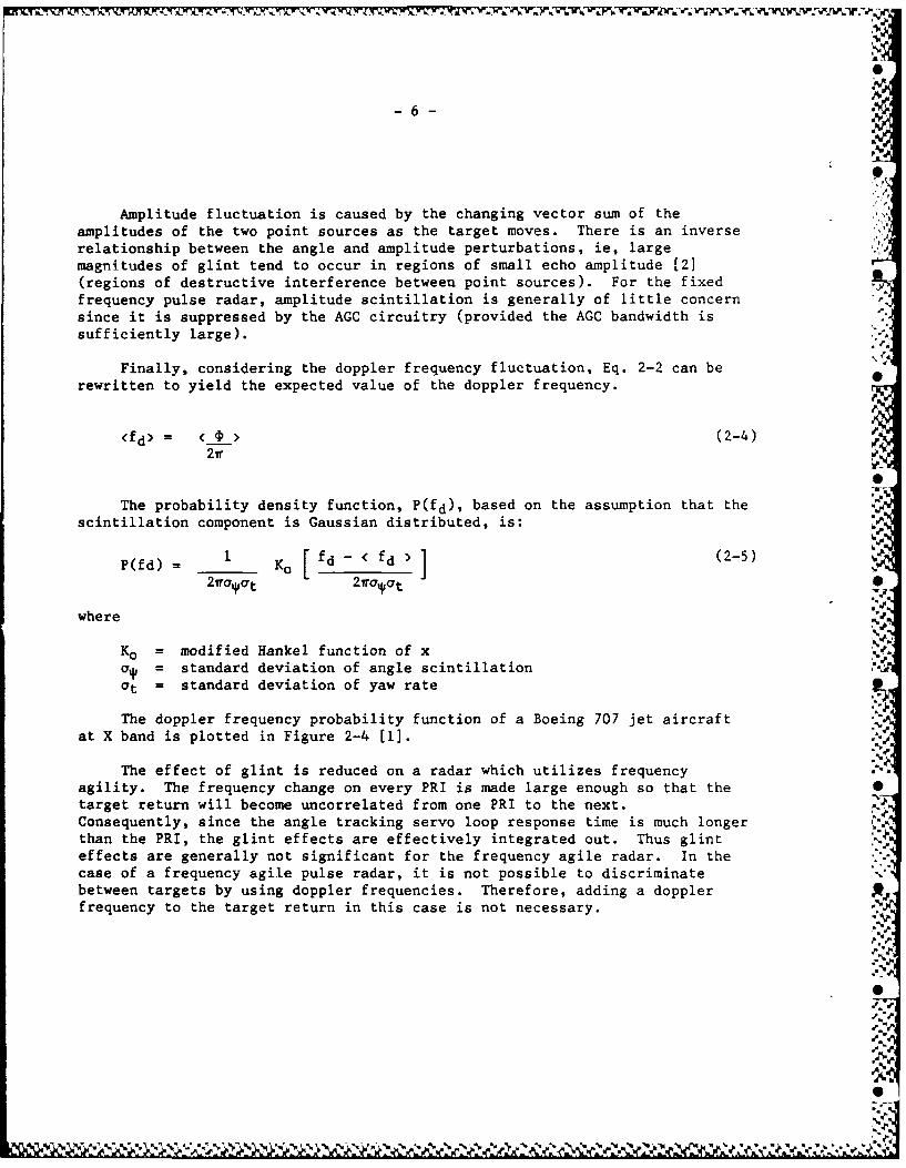
Modelling of real targets is complicated by the fact that they exhibitscintillation and glint, with changing aspect angle, resulting from theirregular shape of the target. The phenomenon of scintillation can be .
explained by considering a target modelled by two point sources. Figure 2-2outlines the phase contours of such a target. The wrinkles on the contours '
are due to the interference of the two sources. Figure 2-3 illustrates the r
incidence of distorted phase contour on the radar antenna. The power flow orPoynting vector is always perpendicular to the phase '-ont as indicated [1].The tracking radar will align its boresight axis so that it is colinear with 5the Poynting vector resulting in a tracking angle error (0). Since the phase .contours fluctuate with time due to the motion of the target, the tracking ,angle error will vary. This is denoted as the angle fluctuation or glint. "C,.?
.S
VC.
4
v
CONTOUR OFCONSTANT PHASE 0
RADAR
FIG. 2-i. Phase Front Radiating From a Point Source
jI T
IAD
FIG. 2-2. Phase Front Radiated From a Two-Element Target

-5-
BORE SIGHTAXIS
COMPLEXTARGET
Oe'
,o
VECTORCONSTANT PHASECONTOURS
~RADAR
FIG. 2-3. Illustration of Angle Scintillation
-6-
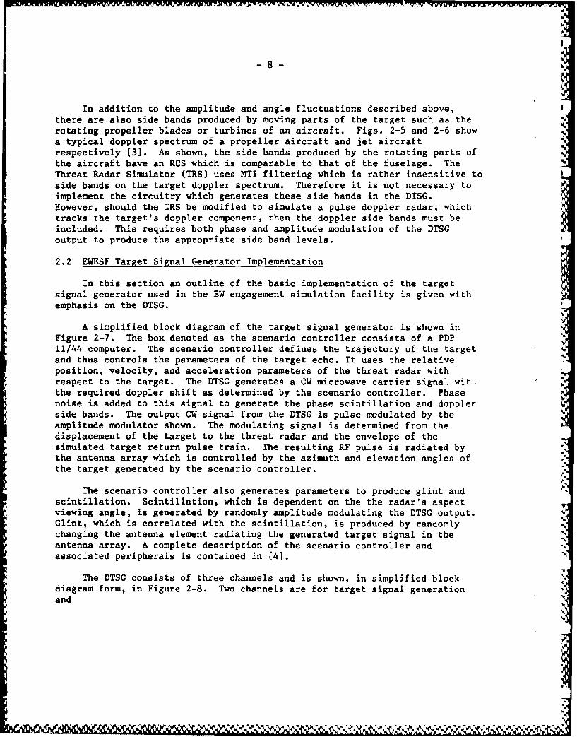
Amplitude fluctuation is caused by the changing vector sum of theamplitudes of the two point sources as the target moves. There is an inverserelationship between the angle and amplitude perturbations, ie, largemagnitudes of glint tend to occur in regions of small echo amplitude [2](regions of destructive interference between point sources). For the fixedfrequency pulse radar, amplitude scintillation is generally of little concernsince it is suppressed by the AGC circuitry (provided the AGC bandwidth issufficiently large).
Finally, considering the doppler frequency fluctuation, Eq. 2-2 can berewritten to yield the expected value of the doppler frequency.
<fd > > (2-4)21r
The probability density function, P(fd) , based on the assumption that thescintillation component is Gaussian distributed, is:
1 Ko [ fd - < fd > (2-5)P(fd) = I__1%L d
21ra at 27rpat 0
where
Ko = modified Hankel function of x114= standard deviation of angle scintillationt= standard deviation of yaw rate
The doppler frequency probability function of a Boeing 707 jet aircraftat X band is plotted in Figure 2-4 [1]. ,
The effect of glint is reduced on a radar which utilizes frequencyagility. The frequency change on every PRI is made large enough so that the 0target return will become uncorrelated from one PRI to the next.Consequently, since the angle tracking servo loop response time is much longerthan the PRI, the glint effects are effectively integrated out. Thus glinteffects are generally not significant for the frequency agile radar. In thecase of a frequency agile pulse radar, it is not possible to discriminatebetween targets by using doppler frequencies. Therefore, adding a dopplerfrequency to the target return in this case is not necessary.
A,

-7-
o .of
+
+
00CY+
*0 L0
-4
0 0CI
Clq 0
C~"4.
64
Jk
-8-
In addition to the amplitude and angle fluctuations described above, P
there are also side bands produced by moving parts of the target such as therotating propeller blades or turbines of an aircraft. Figs. 2-5 and 2-6 showa typical doppler spectrum of a propeller aircraft and jet aircraftrespectively [3]. As shown, the side bands produced by the rotating parts ofthe aircraft have an RCS which is comparable to that of the fuselage. TheThreat Radar Simulator (TRS) uses MTI filtering which is rather insensitive toside bands on the target dopplet spectrum. Therefore it is not necessary toimplement the circuitry which generates these side bands in the DTSG.However, should the TRS be modified to simulate a pulse doppler radar, whichtracks the target's doppler component, then the doppler side bands must beincluded. This requires both phase and amplitude modulation of the DTSGoutput to produce the appropriate side band levels.
2.2 EWESF Target Signal Generator Implementation
In this section an outline of the basic implementation of the targetsignal generator used in the EW engagement simulation facility is given withemphasis on the DTSG.
A simplified block diagram of the target signal generator is shown inFigure 2-7. The box denoted as the scenario controller consists of a PDP11/44 computer. The scenario controller defines the trajectory of the targetand thus controls the parameters of the target echo. It uses the relativeposition, velocity, and acceleration parameters of the threat radar withrespect to the target. The DTSG generates a CW microwave carrier signal wit.the required doppler shift as determined by the scenario controller. Phasenoise is added to this signal to generate the phase scintillation and dopplerside bands. The output CW signal from the DTSG is pulse modulated by theamplitude modulator shown. The modulating signal is determined from thedisplacement of the target to the threat radar and the envelope of thesimulated target return pulse train. The resulting RF pulse is radiated bythe antenna array which is controlled by the azimuth and elevation angles ofthe target generated by the scenario controller.
'*
The scenario controller also generates parameters to produce glint andscintillation. Scintillation, which is dependent on the the radar's aspectviewing angle, is generated by randomly amplitude modulating the DTSG output.Glint, which is correlated with the scintillation, is produced by randomlychanging the antenna element radiating the generated target signal in theantenna array. A complete description of the scenario controller andassociated peripherals is contained in [4].
The DTSG consists of three channels and is shown, in simplified blockdiagram form, in Figure 2-8. Two channels are for target signal generationand

-9-
1.0
0.8- .,Airframe Dopplerw0. Line0.6- lade
FrequencyPrple
0.4 ~ 'DopplerAmplitude Modulation
0.2 S3idebands
0 400 500 1,200 1,600 2,000
DOPPLER FREQUENCY (Hz)
FIG. 2-5. Doppler Frequency Spectrum of a Propeller Driven t~rcraft
1.0.
W0. AirfraI me~0.6- Spectrum
0.4 Turbine7 0.4-Spectrum
0.2 1Turbine0 - - Spectrum
0800 1,600 2,400 3,200 4,000
DOPPLER FREQUENCY (Hz)
FIG. 2-6. Doppler Spectrum of an Approaching single-Engine Turbojet FighterAircraft
A.7

~LWJ JU %. U.~ 'J WW~.UIL J~LW W'A W'J V W.JMU ~ N MU U W MU V W.. '.S .J ~ V~ W~ InsWV y M N,.In u N- d WU
-10-
0,
LU,
-
w -
z
20 u
r___ _ 0
cc CC -4
CL CL O
Lu L U
WU-j CC Z
0c >
Ow 00 0
0g* 5 -a
U)
z aCA
060
LL..
0 00
20I
<[Z

w a cc
D 00 c r 0C
<00 o<
o 0
0 . .0 u0
0 0 0WO 0 -0 0w
'( < LZ
V-04
0 0 .
-< 04
0- w> 0
i-C
0~
R CC
- 12 -
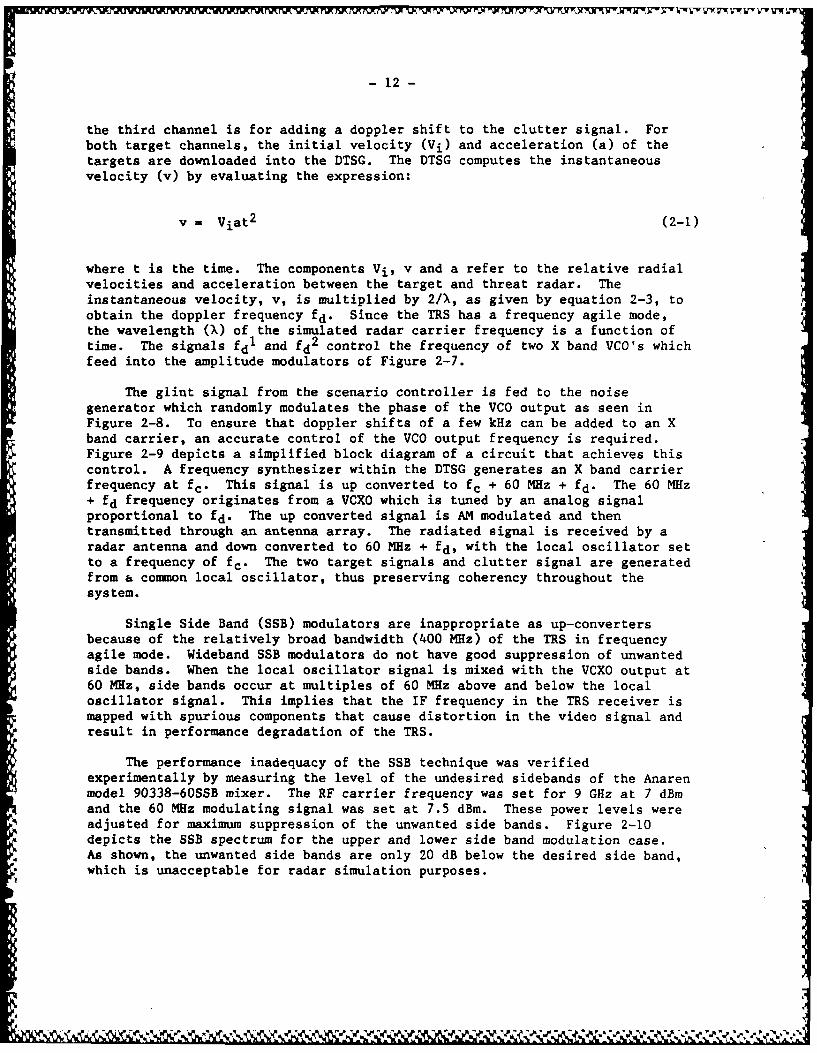
the third channel is for adding a doppler shift to the clutter signal. Forboth target channels, the initial velocity (Vi) and acceleration (a) of thetargets are downloaded into the DTSG. The DTSG computes the instantaneousvelocity (v) by evaluating the expression:
v = Viat2 (2-1)
where t is the time. The components Vi, v and a refer to the relative radialvelocities and acceleration between the target and threat radar. Theinstantaneous velocity, v, is multiplied by 2/X, as given by equation 2-3, toobtain the doppler frequency fd" Since the TRS has a frequency agile mode,the wavelength (X) of the simulated radar carrier frequency is a function oftime. The signals fd1 and fd2 control the frequency of two X band VCO's whichfeed into the amplitude modulators of Figure 2-7.
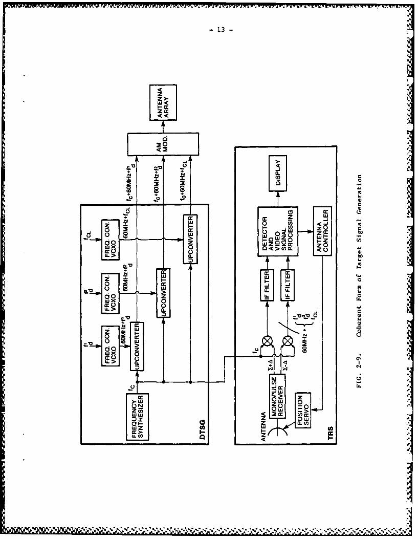
The glint signal from the scenario controller is fed to the noisegenerator which randomly modulates the phase of the VCO output as seen inFigure 2-8. To ensure that doppler shifts of a few kHz can be added to an Xband carrier, an accurate control of the VCO output frequency is required.Figure 2-9 depicts a simplified block diagram of a circuit that achieves thiscontrol. A frequency synthesizer within the DTSG generates an X band carrierfrequency at fc- This signal is up converted to fc + 60 MHz + fd" The 60 MHz+ fd frequency originates from a VCXO which is tuned by an analog signalproportional to fd. The up converted signal is AM modulated and thentransmitted through an antenna array. The radiated signal is received by aradar antenna and down converted to 60 MHz + fd, with the local oscillator setto a frequency of fc- The two target signals and clutter signal are generatedfrom a common local oscillator, thus preserving coherency throughout thesystem.
Single Side Band (SSB) modulators are inappropriate as up-convertersbecause of the relatively broad bandwidth (400 MHz) of the TRS in frequencyagile mode. Wideband SSB modulators do not have good suppression of unwantedside bands. When the local oscillator signal is mixed with the VCXO output at60 MHz, side bands occur at multiples of 60 MHz above and below the localoscillator signal. This implies that the IF frequency in the TRS receiver ismapped with spurious components that cause distortion in the video signal andresult in performance degradation of the TRS.
The performance inadequacy of the SSB technique was verifiedexperimentally by measuring the level of the undesired sidebands of the Anarenmodel 90338-60SSB mixer. The RF carrier frequency was set for 9 GHz at 7 dBmand the 60 MHz modulating signal was set at 7.5 dBm. These power levels wereadjusted for maximum suppression of the unwanted side bands. Figure 2-10depicts the SSB spectrum for the upper and lower side band modulation case.As shown, the unwanted side bands are only 20 dB below the desired side band,which is unacceptable for radar simulation purposes.
61 A0
-13 -
z
w <9
(/0
w0 0)-4-
- - -- aL -Zr
0 u0 S2 J z 0ui x < >U)zom 0 < QLLwZ >*-
> LL00 z
2 Li
0-
0 >zN
4.. >
>- w 0 U
LU UJ< 2 m U) c
I-L Z o ccr. -D
_ _ _ _ _ _ _ _cc

-14-1
-10
-30 - - --
dBm
-50
II
-70
8.82 8.94 9.0 9.06 9.18 9.30
t FREQUENCY (GHz)
(L.Q. freq)
(a)
-10
-3 0 - .-"
dBm
-60'"
-70
8.82 8.94 9.0 9.06 9.18 9.30
t FREQUENCY (GHz)(LO. freq)
(b)
FIG. 2-10. Output Spectra of SSB Modulatora) UPPER SIDEBAND MODUTATIONb) LOWER SIDEBAND MODULATION
N''-
5

- 15 -
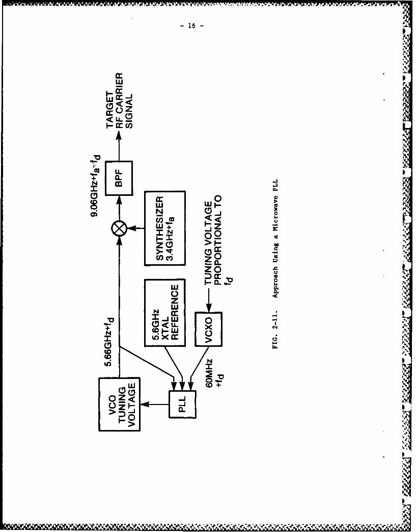
To avoid problems with spurious side bands, the up-conversion stage wasdesigned using a phase locked loop (PLL) approach. Figure 2-11 shows a blockdiagram of one of the three channels. A microwave VCO is phase locked to thesum frequency of a 5.6 GHz reference source and the VCXO output at 60 MHz + fd-The resulting VCO output at 5.66 GHz + fd is up-converted by a synthesizer,operating at 3.4 GHz + fa, where fa is the frequency agility component. Thespurious components at the output of the VCO and synthesizer mixer are notmapped onto the 60 MHz IF, as was the problem with the SSB method. In thefollowing section, details of the DTSG RF design are given.
3.0 DTSG RF Design
3.1 Introduction
The RF design of the DTSG is based on a phased lock loop (PLL) circuitwhich is shown in the block diagram of Figure 3-1. The PLL consists of avoltage control oscillator (VCO), a low pass loop filter, and two frequencymixers. The VCO output is down-converted to DC through mixers MI and M2. Theoutput of the second mixer, M2, is filtered and biased by the Loop filterwhich tunes the VCO to the required frequency of 5.66 GHz + fd" This signalis up-converted by mixer M3 to produce the output signal of 9.06 GHz + fa + fd(where fa is the frequency agility). The loop filter is described in furtherdetail in section 3.2.
When the DTSG is not being utilized, i.e. prior to a trial run, the VCXOis stabilized to exactly 60 MHz by the VCXO frequency stabilizer. Thestabilizer measures the voltage required to tune the VCXO to 60 MHz and usesit as an offset voltage for the VCXO during the trial run. Since trials lastfor no more than a few minutes, the frequency drift of the VCXO isnegligible. The stabilizer is described in more detail in section 3.4.
The frequency counter, shown in Figure 3-1, provides immediate feedbackfor the operator calibrating the system. The circuitry is described insection 3.5.
3.2 Loop Filter Used in PLL
3.2.1 General
The system operates under two modes denoted as search and lock, which arebriefly described below. A block diagram of the loop filter is shown inFigure 3-2.
Search Mode
The phase lock loops are unlocked when power is initially applied to theDTSG. To establish phase lock, the VCO frequency is scanned over a range ofapproximately 100 MHz. The scanned frequency range is adjusted so that theloop circuit locks onto the required upper side band of 5.6 GHz + 60 MHz + fd(as opposed to the lower side band of 5.6 GHz - 60 MHz - fd)"
V.v%
-16 -
cc D
U.
cc 0 >4
N) a 0CO ccLu Z
) 0 0.
z 0 ADW
+~U 0,JL
R- 1U-xz
wp
-J xLJ-w >N*
wp

-17 -
Z~~~Z w mma z
00 -a
a. P m .ZCL Z ;:00r
00o
-4J
Uj LLI -4
00
ZU. 0
x 0
't f w z
017 U.
C-I-
0) 0
(9 0
ccNL
W NN N N~I ~ . ~' P ~cc

-18-
m U)
w CL,
ww1-0 L 0 -
0> o0 cZ LL,
w WOO
jr 0w~ 3:a
w a cc LI 51.-0cr WCL V
Si 0 5. cU) ag -i V
sLL .1 0 x wLL 0 a -1 3: 4 CC c
4.J
C, 0
09 0
0I0->-S
ui cr N c
r-u
a KI
-19 -
Lock Mode
When the scanned frequency approaches the upper side band, the rampsignal is disabled and a loop filter is switched into the circuit which closes peach PLL. The loop filter consists of a lag/lead filter with a 3 dB bandwidthof 100 Hz. The filter enables the PLL circuit to track the changes in thedoppler frequency. This filter is in parallel with a compensated integratorfilter which has a long time constant designed to compensate for drift in theVCO tuning voltage characteristics.
Detailed explanations of the hardware used to implement the two modes ofoperation are now given.
3.2.2 Search Mode
The circuit used to generate the search mode is illustrated in the blockdiagram of Figure 3-2. In search mode, the ramp signal from the ramp voltagegenerator is fed to the summer network via the sample and hold circuit. Theremaining three inputs to the summer originate from the lock loop filtercircuitry. The output of the summer drives the VCO frequency control througha 3rd order Butterworth low pass filter of 1 MHz bandwidth. It is inserted toreduce the high frequency noise and the 60 MHz spurious signals which leak Ithrough the lag/lead filter.
The ramp signal allows the VCO to be scanned over a frequency range of100 MHz. An offset voltage is superimposed on this ramp voltage so that thecenter of the frequency scan is approximately 5.66 GHz.
When the VCO frequency is near 5.66 GHz + fd, the frequency of the phasedetector output will be within the passband of the lock detection low passfilter (see Figure 3-2). The envelope detection will then exceed apre-determined threshold and set the RS flip flop, making the search/locksignal low. This signal causes the sample and hold circuit to hold thepresent value of the ramp signal which in turn will keep the tuning voltage ofthe VCO constant.
The time constant of the envelope detection circuit is about 10- 3 sec andthe bandwidth of the lock detection low pass filter is 100 kHz. Consequently,to ensure that the detection circuit will respond to the VCO as it scansthrough the frequency of 5.66 GHz, the scan time through a 200 kHz range(twice the filter bandwidth) should be sufficiently greater than 10- 3 sec. Asafe maximum scan rate chosen is 20 MHz/sec. The repetition period of theramp signal is 5 seconds. Since the modulation sensitivity of the VCO isapproximately 20 MHz/volt, the peak ramp signal is set at approximately5 volts.
Figure 3-3 depicts the circuit used for lock detection in the PLL whileFigure 3-4 illustrates the timing diagram for the lock up procedure. Listedbelow are the sequential steps of the lock up procedure.
.6P

-20-
LOCK ATTEMPTENABLEI "
.lsec
SHOT I
RESET ,.
LOST LOCK DET. r',
THRESHOLD >CK Q
FROM COMPARATORPHASE DETECTOR
S
D SEARCH/LOCK
.Set
LOCK DET
COMPARATOR
L.5,
THRESHOLD
PASS ENVELOPE__:'•
FILTER DETECTOR105 Hz BW
FIG. 3-3. Circuitry Used For Lock Detection .,..;0

-21-
RAMP
,4-----SEARCH NoITRCI.,PHASE ACQUISITION
I OF LOOP I
DETECTOROUTPUT
THRESHOLD LEVEL
ENVELOPEDET.OUTPUT ____
LOCKDET.
LOCK .secATTEMPTENABLE
SEARCH/
.4K
FIG. 3-4. Timing Diagram of Lock Up
i 4Ak
4'k
* *' ',:, ;''.'""'I"" ";. " ,'.' o, ", ,.J'...;,? ' ''',. '' "" , '.' , ,"r v .- Y "-, % '""" - - -

-22-
1) Upon reset, the RAMP signal tunes the VCO toward the desiredfrequency of 5.66 GHz + fd"
2) As the VCO frequency approaches 5.66 GHz + fd, the frequency at thephase detector output decreases. When the VCO frequency is within100 kHz of 5.66 GHz + fd (i.e. within the bandwidth of the low passfilter), the envelope detector output begins to increase in amplitude.
3) The envelope detector output exceeds the threshold value when the VCOfrequency is within a few tens of kHz from 5.66 GHz + fd" At thistime the LOCK DET signal goes high, causing the SEARCH/LOCK signal togo low.
4) Upon receiving a low SEARCH/LOCK signal, the sample and hold circuitsamples the ramp voltage and holds it, keeping the VCO tuning voltageconstant.
5) Finally, the Lock loop filter (see Figure 3-2) is switched into thecircuit and the PLL locks up.
Should the attempt for lock up fail, the LOST LOCK DET signal willcontinue oscillating, thus resetting the search/lock flip flop. This willcause the search mode to be reactivated.
Since the PLL requires some time to lock up, the LOCK ATTEMPT ENABLEsignal is activated for 0.1 second each time the PLL goes into Lock mode.This prevents the LOST LOCK DET signal from resetting the SEARCH/LOCK flipflop for 0.1 sec after the loop enters lock mode. Consequently the loop has0.1 sec to attempt phase lock. If the lock up is successful then the LOST %LOCK DET signal is not active.
The status of the SEARCH/LOCK signal is indicated by an LED on the frontpanel. It can also be read by the host computer through the computerinterface. When the DTSG is powered up, the host computer strobes the RESETLine to initially start the loop filter in search mode.
3.2.3 Lock Mode J'
The lock mode is initiated when the SEARCH/LOCK signal goes low. Aspreviously discussed, this engages the lock loop filter which closes theindividual PLL circuits. As shown in Figure 3-2, the lock loop filterconsists of a lag/lead network and an integrator with phase compensation. '"
The lag/lead filter has a 3 dB bandwidth of about 100 Hz. It is designedto respond to the required change in VCO frequency due to the changing dopplerfrequency. The frequency hold range provided by the lag/lead filter isapproximately 4 MHz. Keeping the hold range small ensures that the VCO outputhas a high spectral purity and the PLL circuit maintains high stability.Difficulty arises in acquisition however if the hold range is made any smallerthan 4 MHz*.
(*) Theoretically, the lower limit of the hold range is the dopplerfrequency range requirement of about 150 kHz. I1
- C.... , . , , , . . . ..- , .... ,, ,- . . . '- C..,-,-* C- -
-23-
Unfortunately, the tuning characteristics of the VCO are very sensitiveto temperature fluctuations. For the models used in the DTSG, the deviationcan be as high as 2 MHz/°C. Since the frequency hold range of the lag/lead Sfilter is only 4 MHz, a 20C change in temperature will cause the loop to loselock. This drift is compensated by the compensated integrator circuit. Thetime constant of the compensated integrator is large enough so that it doesn'tinterfere with the operation of the lag/lead filter. The integrator networkalso compensates for the drop in the voltage of the holding capacitor used inthe sample and hold circuitry (used to hold the ramp voltage on the search tolock transition).
As shown in Figure 3-2, the output of the loop filter passes through a
3rd order Butterworth low pass filter prior to entering the frequency control
input of the 5.6 GHz VCO. The filter has a bandwidth of 2 MHz and is requiredto prevent the 60 MHz harmonic components, generated on the output of mixer M2 S
(see Figure 3-1), from propagating through the lock loop filter. Although thelock loop filter is essentially a low pass filter, it contains activecomponents that have bandwidths of up to 60 MHz. Therefore, the extra lowpass filter ensures that no spurious components (at 60 MHz multiples from thecarrier) reach the VCO input. The frequency response of the filter is shownin Figure 3-5.
3.3 Performance of Microwave PLL '
The spectrum of the VCO output, measured in the locked condition at5.66 GHz with the VCXO adjusted to 60 MHz, is shown in Figure 3-6. Note thatthe spurious components, at multiples of 60 MHz from the carrier, are L..re Sthan 50 dB below the carrier. This is a 30 dB improvement over thealternative method of SSB modulation that was discussed earlier. The spuriousside bands are not produced by the VCO but by mixer Ml of Figure 3-1. Toovercome this problem, an isolator was placed between the power splitter PIand mixer Ml.
As mentioned earlier, the 5.66 GHz signal is mixed with a 3.4 GHz sourceto produce a target output signal of 9.06 GHz. Over a frequency span of 50MHz, the DTSG output, shown in Figure 3.7(a), contains spurious noise that is50 dB below the main carrier. To measure this performance in terms ofquality, the output of the DTSG is compared with that of a high precisionHP8672A synthesizer. Set at 9.06 GHz, the HP8672A produces a noise floor that S
is 55 dB below the carrier, as indicated by Figure 3.7(b). The DTSG is ".generating a noise floor that is only 5 dB higher than that of the expensiveand elaborate HP8672A synthesizer. Therefore, the DTSG is considered to be anideal RF source for generating realistic target return signals for the ThreatRadar Simulator.
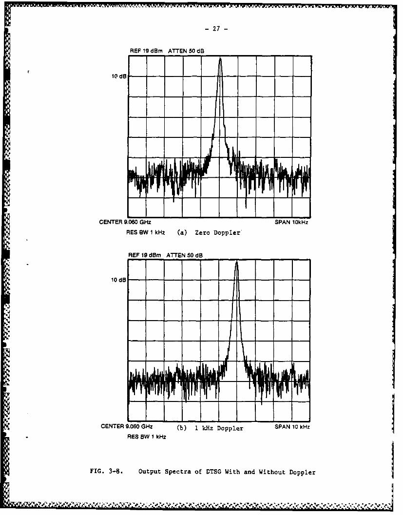
A closer view of the spectral output of the DTSG, operating at zerodoppler, is shown in Figure 3.8(a). The diagram confirms that no spectralnoise exists within the target doppler band, which at X-band can range from0 to 60 kHz, representing velocities of 0 to 10OOm/sec respectively. In IFigure 3.8(b), a doppler component of fd=lOkHz is added to the DTSG output to
" m J J "t' " "' " " 0 ',- ' %",J""' t. '. "K" &" l,, - %1 ".. % ' -*% ' S

-24-
0
C.4
0
CL
0
LL0
0m
O 0O
cm LO
(SP) NIVE
-25-A
- - NM
zo
<cn
coo
0 EDcr) C/)
- - Nco>1
z C.,
NU

-26-
REF 20 dBm ATTEN 50 dB
"%" CARRIERl0dB -- -- -- -- -- -
CENTER 9.060 GHz SPAN 50 MHz
I
REF 20 d~m ATTEN 50 dB
'CARRIER
4*K0.
,4
CENTER 9.060 GHz (b) HP8672A SPAN 50 MHz
RES BW 10 kHz
FIG. 3-7. Comparing the Output Spectrum of the DTSG with an HP8672ASynthesizer set at 9.06 GHz
" " CARIER I
10 dB ..,,
4|*
- - a,. t~~k*r~w *r ~ I
-27-
REF 19 dBm ATTEN 50dB
CENTER 9.060 GHz SA 0~
RES BW 1 kHz (a) Zero Doppler'
REF 19 dBm ATTEN 50dB
CENTER 9.060 GHz (b I kHz Doppler SPAN 10 kHzRES BW 1 kHz
FIG. 3-8. Output Spectra of DTSG With and Without Doppler

- 28 -
represent a target travelling at 166m/sec. It is observed that the PLLprocess, used to mix the doppler signal with the 5.66 GHz source, does notalter the carrier signal or introduce spurious noise within the target dopplerband. In contrast, the SSB technique introduces spurious components atmultiples of the doppler frequency away from the carrier onto the output.This produces many false targets travelling at different velocities. Thus theDTSG, using the PLL circuit, is ideal for generating doppler componentswithout affecting the target spectral profile or creating false targets.
3.4 VCXO Frequency Stabilization
VCXO's are generally very difficult to mechanically tune, and once set tothe desired frequency, they tend to drift in time. To avoid these tuningproblems, an automatic tuning circuit was implemented. The circuit isactivated prior to running a scenario and locks the VCXO's to a 60 MHzreference frequency. The bias voltages required to tune the VCXO's aredigitized. During run time, the bias voltage is added to the frequency tuningvoltage from the VCXO driver. The short term drift of the VCXO is only ± 2Hzmeasured over several minutes, which is negligible.
A block diagram of the VCXO stabilization circuit is shown in Figure 3-9.The VCXO is initially locked to a 60 MHz reference immediately following theclosing of SWl. The loop filter, which is a phase compensated integrator,provides the proper filtering at the output of the mixer. When SW2 is closed,the counter begins to count up or down, depending on the sign of theintegrator output. The D/A converter output changes until the loop filteroutput is zero. When the run sequence begins, SW2 is opened causing the D/Aoutput to remain locked at its present level. When SWl is opened, the VCXOgenerates the correct doppler frequency proportional to the doppler controlinput.
SWl and SW2 are controlled by the STAB command which originates from thehost computer. Consequently, stabilization is achieved through softwarecontrol.
3.5 Doppler Frequency Monitor
The doppler frequency monitor is a dual channel frequency counter whichmonitors the average doppler frequency of the two targets. The averaging iscalculated over a 0.1 second or 1.0 second interval, as selected by theoperator. An LED display indicates the doppler frequency of both channels.
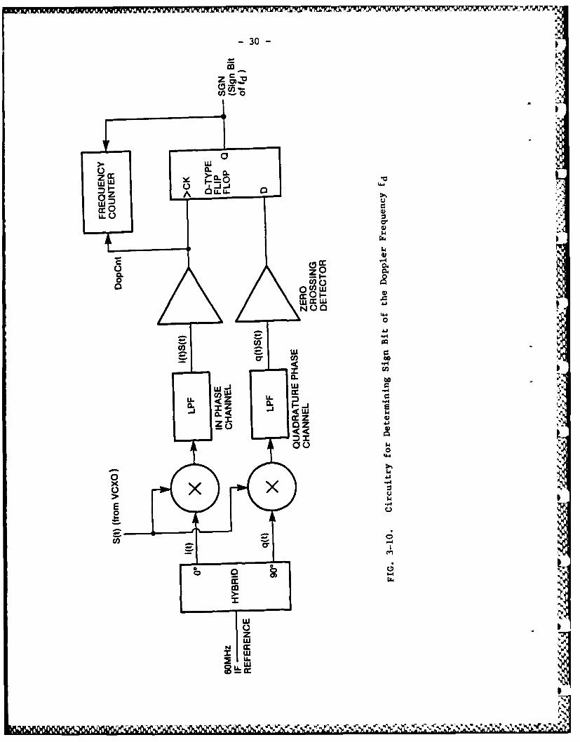
The monitor determines the doppler sign (positive or negative) through Iand Q channel demodulation of the VCXO signals. A block diagram of themonitor is shown in Figure 3-10. A brief explanation of its operation is nowpresented. Let the VCXO signal be denoted by s(t) and given by
s(t) = cos (21r(fif + fd)t + ) (3-1)

-29-
rz
w0
LL-
w'
xN
zi 0.4rq0 0 co
0
cra
IL, 0
cr 0
zz
0
A ~ ~ A ~ '- ~ ~% ~ V ~v ' ~ ' *--Q;
-30-
co) -0
LUU
w w4D
[ a
w4 D
cr.0e
UU'
0r 0
u..
U. 0
E~ -4
00rnz
0 S'S
;mwz --4
w vi
cn W c
<S Z S 'S'
- 31 -
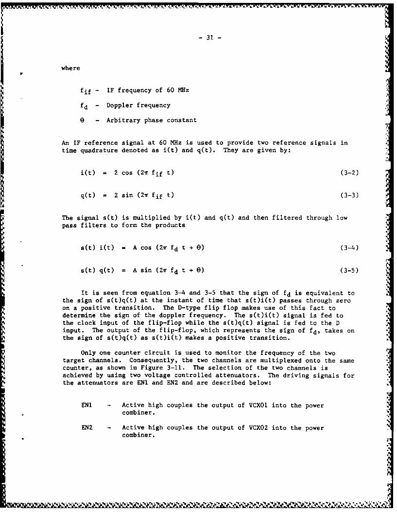
where
fif - IF frequency of 60 MHz
fd - Doppler frequency
e - Arbitrary phase constant
An IF reference signal at 60 MHz is used to provide two reference signals intime quadrature denoted as i(t) and q(t). They are given by:
i(t) = 2 cos (21 fif t) (3-2)
q(t) = 2 sin (21 fif t) (3-3)
The signal s(t) is multiplied by i(t) and q(t) and then filtered through lowpass filters to form the products
s(t) i(t) = A cos (2w fd t + e) (3-4)
s(t) q(t) = A sin (21 fd t + e) (3-5)
It is seen from equation 3-4 and 3-5 that the sign of fd is equivalent tothe sign of s(t)q(t) at the instant of time that s(t)i(t) passes through zeroon a positive transition. The D-type flip flop makes use of this fact todetermine the sign of the doppler frequency. The s(t)i(t) signal is fed tothe clock input of the flip-flop while the s(t)q(t) signal is fed to the Dinput. The output of the flip-flop, which represents the sign of fd, takes onthe sign of s(t)q(t) as s(t)i(t) makes a positive transition.
Only one counter circuit is used to monitor the frequency of the twotarget channels. Consequently, the two channels are multiplexed onto the samecounter, as shown in Figure 3-11. The selection of the two channels isachieved by using two voltage controlled attenuators. The driving signals forthe attenuators are ENI and EN2 and are described below:
ENI - Active high couples the output of VCX01 into the powercombiner.
EN2 - Active high couples the output of VCX02 into the powercombiner.
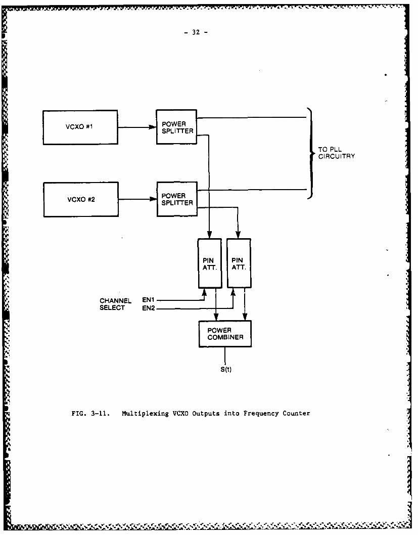
-32-
VCXO #1POE SPLITTER
TO PLLCIRCUITRY
VOXO #2POEJ
ATT ATT.
I
SM ,
FIG 3-1 MutpeigVX uptsit rqec one
-33-
The signals passed to the frequency counter are (See Figure 3-10):
Dop Cnt - Zero detected form of i(t) in TTL compatible signal format.
SGN - Sign of the doppler frequency. SGN is high if the dopplerfrequency is positive.
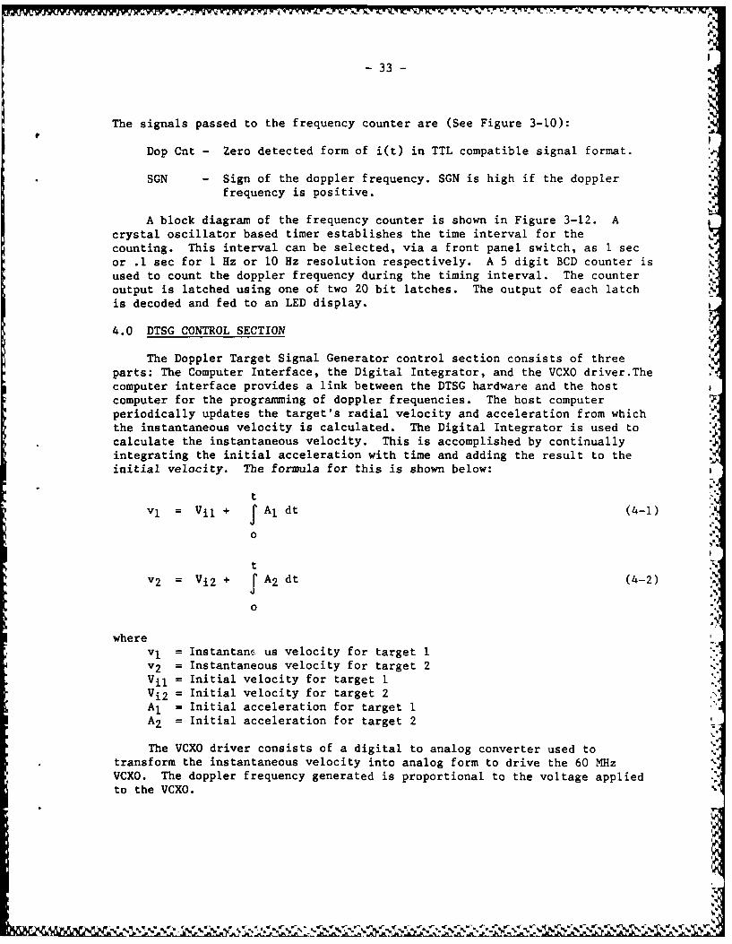
A block diagram of the frequency counter is shown in Figure 3-12. Acrystal oscillator based timer establishes the time interval for thecounting. This interval can be selected, via a front panel switch, as 1 secor .1 sec for 1 Hz or 10 Hz resolution respectively. A 5 digit BCD counter isused to count the doppler frequency during the timing interval. The counteroutput is latched using one of two 20 bit latches. The output of each latchis decoded and fed to an LED display.
4.0 DTSG CONTROL SECTION
The Doppler Target Signal Generator control section consists of threeparts: The Computer Interface, the Digital Integrator, and the VCXO driver.Thecomputer interface provides a link between the DTSG hardware and the hostcomputer for the programming of doppler frequencies. The host computerperiodically updates the target's radial velocity and acceleration from whichthe instantaneous velocity is calculated. The Digital Integrator is used tocalculate the instantaneous velocity. This is accomplished by continuallyintegrating the initial acceleration with time and adding the result to theinitial velocity. The formula for this is shown below:
vI = Vil + Al dt (4-1)
0
t
v2 = + f A2 dt (4-2)
0
wherevl = Instantan6. us velocity for target Iv2 = Instantaneous velocity for target 2Vil = Initial velocity for target 1Vi2 = Initial velocity for target 2A1 = Initial acceleration for target 1A2 = Initial acceleration for target 2
The VCXO driver consists of a digital to analog converter used totransform the instantaneous velocity into analog form to drive the 60 MHzVCXO. The doppler frequency generated is proportional to the voltage appliedto the VCXO.

-34-
CHANNEL 1 CHANNEL 2
LED LED
Display Display
35 35
DECODER DEC DE
,
IILAT" CH LATCH
Latch Data Data Latch-T---1-20 20
SIGNAL iN Count 5 DIGIT
-0 Gate BCD COUNTER
TIMER
FIG. 3-12. Block Diagram of Frequency Counter
Diagr-m I

-35-
5.0 CONCLUSION
The Threat Radar Simulator (TRS) used in the Electronic WarfareEngagement Simulation Facility (EWESF) at DREO includes a Moving TargetIndicator (MTI) processor. The MTI circuit makes use of the doppler frequencyshift associated with moving targets to distinguish the target return fromclutter. To provide the MTI processor with the necessary doppler frequency, aDoppler Target Signal Generator (DTSG) was developed at DREO. The DTSG canproduce positive or negative doppler shifts to simulate targets that aretravelling toward or away from the radar respectively. Although the ThreatRadar Simulator at DREO is a non-coherent system, the DTSG is capable ofproviding phase perturbations that can be detected by a coherent radar. Thisis an important consideration since phase fluctuation in the pulse returnsprovides significant information to the radar about the target's spectralprofile. Therefore in the event that the TRS should become coherent, the DTSGis capable of providing the necessary doppler side bands that arerepresentative of real targets.
Due to the receiving sensitivity of the tracking radar, it is imperativethat the DTSG produce doppler frequencies that contain very low spuriousfrequency components or unwanted side-bands at multiples of the IF frequency.For this reason, a phase lock loop (PLL) approach was used instead of theconventional Single Side Band technique for modulating the carrier frequencywith the doppler frequency. Experimental results show that the PLL methodprovides up to 30 dB of spurious noise improvement over the SSB technique.This is an important consideration since it is essential that the trackingperformance of the radar not be compromised due to poor target simulation.
6.0 REFERENCES
[1] Dunn, Howard, "Radar Target Amplitude, Angle, and Doppler Scintillationfrom Analysis of the Echo Signal Propagating in Space", IEEE Transactionson Microwave Theory and Techniques, Vol MTT-16, No. 9, Sept. 1968.
[2] HiTech Canada Ltd., "Glint Characteristics and Simulation FeasibilityStudy", April 1979.
[3] Nathanson, Fred E., "Radar Design Principles", McGraw Hill 1969.
[4] Moffat, John W., Private Communication.
-A?
a,.'
a,¢

-37-UNCLA SSTFIFD
SECURITY CLASSIFICATION OF FORM(highest classification of Title, Abstract, Keywords) .
DOCUMENT CONTROL DATA(Security cliification of title, body of absitrct and indexing anotation must be entered when the overall documont a classified)
ORIGINATOR (the name and address of the organization preparing the document 2. SECURITY CLASSIFICATION
Organizations for whom the document was prepared. e.g. Establishment sponsoring (overall security classification of the documenta contractor's report, or tasking agency, are entered in section 8.) including special warning terms if applicabie)
NATIONAL DEFENCEDEFENCE RESEARCH ESTABLISHMENT OTTAWAOTTAWA, ONTARIO KIA 0Z4 UNCLASSIFIED
3. TITLE (the complete document title as indicated on the title page. ItS classification should be indicated by the appropriate
abbreviation (S.C.R or U) in parentheses after the title.)
DOPPLER TARGET SIGNAL GENERATOR (U)
4. AUTHORS (Last name. first name. middle initial. If military. show rank, e.g. Doe, Mal. John E.)
DOUCET, KEITH R. AND NIELSON, JOHN
5. DATE OF PUBLICATION (month and year of publication of 6a NO. OF PAGES (total 6b. NO. OF REFS (total cited indocument) containing information. Include document)
APRIL 1988 Annexes, Appendices. etc.)
35 46. DESCRIPTIVE NOTES (the category of the document. e.g. technical report, technical note or memorandum. If appropriate. enter the tyce of
report. e.g. interim. progress. summary, annual or final. Give the inclusive dates when a specific reporting period is covered.)
TECHNICAL NOTE
B. SPONSORING ACTIVITY (the name of the department project office or laboratory sponsoring the research and development Include theaddress.)
9a. PROJECT OR GRANT NO. (if appropriate, the applicable research 9b. CONTRACT NO. (if appropriate, the applicable number unoerand development project or grant number under which the document which the document was written)was written. Please specify whether project or grant)
041LD11
10a. ORIGINATOR'S DOCUMENT NUMBER (the official document 10b. OTHER DOCUMENT NOS. (Any other numbers which maynumber by which the document is identified by the originating be assigned this document either by the originator or by theactivity. This number must be unique to this document.) sponsor)
DREO TECHNICAL NOTE NO.88-14
1 1. DOCUMENT AVAILABILITY (any limitations on further dissemination of the document, other than those imposed by security cessificaton
IX) Unlimited distribution(I Distribution limited to defence departments and defence contractors; further distribution only as approved
D ) istribution limited to defence departments and Canadian defence contractors; further distribution only as approved
( Distribution limited to government departments and agencies; further distribution only as approved
I } Distribution limited to defence departments; further distribution only as approved
I ) Other (please specify.
12 DOCUMENT ANNOUNCEMENT (any limitation to the bibliographic announcement of this document. This will normally correspond tothe Document Availabilty (11). However. where further distribution (beyond the audience specified it 11) is Possible, a widerannouncement audience may be selected.)
UNCLASSIFIED
SECURITY CLASSIFICATION OF FORM
OC003 2/C6187

-38- UNCLASSIFIED
SECURITY CLASSIFICATION OF FORM
13. ABSTRACT ( a brief ano factual summary of the document. It may also apear elsewhere in the body of the document ,self it is ignv i
desirable that the abstract of classifieo documents be unclassified. Each Paragraph of the abstract shall begin with an indication of tIlesecurity classification of the information in the paragraph (unleSs the document itself is unclassified) represetled as (S). (V. (R). or (U!Itis not necessary to Include here abstracts in both officai languages unless the text is bilingual). b
(U) The Threat Radar Simulator (TRS), utilized in DREO's ECM facility, is equipped
with a Moving Target Indicator (MTI) processor used to detect the skin echo of moving
targets. The MTI unit makes use of a doppler shift, associated with the moving target,
to discriminate between the target and unwanted clutter. To facilitate the MTI's
requirement for doppler shifts in the return pulses, a Doppler Target Signal Generator
(DTSG) has been developed at DREO. The DTSG is an X-band programmable frequency
synthesizer with three independent outputs. Two of the outputs are used in the generatio
of target returns and the third output provides a doppler shift to the clutter return
signal..-,
I .. - -.- .--
14. KEYWORDS. DESCRIPTORS or IDENTIFIERS (technically meaningful terms or short phrases that characterize a document and could behelpful in cataloguing the document They should be selected so that no security classification is required. Identifiers, such as equipmentmodel designation, trade name. military project code name. geographic location may also be included. if possible keywords should be selecle-from published thesaurus. e.g. Thesaurus of Engineering and Scientific Terms (TEST) and trat thesaurus-identified. If it is not Possible :oselect indexing terms which are Unclassified. the classification of each should be indicated as with the title.)
Doppler Generator)Doppler Target Signal Generator,PLL,DopplerTRSThreat Radar Simulator,,
%
UNCLAS SIFIlED
SICfLAITY CLASSIFICATION OF F¢OAM___ _ _ _ Ifed .o