Dokumentvorlage für Diplomarbeiten und …€¦ · Web viewOlivia Vidoni was my immediate tutor...
211
ELECTRICAL PROPERTIES OF AU 55 CLUSTER SYSTEMS Inauguraldissertation zur Erlangung des Grades eines Doktors der Naturwissenschaften (Dr. rer. nat.) vorgelegt dem Fachbereich Chemie der Universität Essen von Viktória Torma aus Ungarn Essen Januar 2002
-
Upload
nguyenthien -
Category
Documents
-
view
214 -
download
0
Transcript of Dokumentvorlage für Diplomarbeiten und …€¦ · Web viewOlivia Vidoni was my immediate tutor...

ELECTRICAL PROPERTIES OF
AU55 CLUSTER SYSTEMS
Inauguraldissertation
zur Erlangung des Grades eines
Doktors der Naturwissenschaften
(Dr. rer. nat.)
vorgelegt dem Fachbereich Chemie
der Universität Essen
von
Viktória Torma
aus Ungarn
Essen Januar 2002
Hiermit bestätige ich, die Arbeit nur mit den angegebenen Hilfsmitteln ohne fremde Hilfe
angefertidt zu haben
Viktoria Torma
Vorsitzender: Prof. Dr. Frank-Gerrit Klärner
1. Gutachter: Prof. Dr. Gunter Schmid
2. Gutachter: Prof. Dr. Ulrich Simon
Tag der mündlichen Prüfung:
ii

To my best friend and husband, Zoli
iii

Acknowledgment
The present Ph.D. thesis has been completed between September 1998 and November
2001 in the Institute of Inorganic Chemistry, University of Essen.
First I would like to thank to my scientific supervisor,
Prof. Dr. Günter Schmid
for the interesting research topics and his continuous motivation, for the numerous stimu-
lating discussions and the freedom in the work as well. His help in the most complicated
problems was indispensable for the success of this study.
I am indebted also to Prof. Dr. Ulrich Simon for the valuable discussions on the physical
aspects. He introduced me in the amazing field of nanoelectronics from the very first mo-
ment, helped me in the measurements and finally took over the role of the second referee
to my thesis.
I thank to Prof. Dr. Frank-Gerrit Klärner for his participation by defending my doctoral
thesis.
Olivia Vidoni was my immediate tutor in the organic synthetic work. She helped also with
some of the electrical conductivity measurements. I thank her kindly cooperation these im-
portant stages of my research.
Torsten Reuter is thanked for valuable discussions. I thank to Steffen Franzka the AFM
measurements and his critical comments. Ursula Giebel is thanked for the synthesis of
Au55(PPh3)12Cl6.
I am indebted to the whole research group for the support and the good atmosphere.
I thank to Matthias Schumann und Prof. Dr. C. Radehaus (University of Chemnitz) for the
external cooperation and for the probes fabricated by electron beam lithography.
Finally I thank to Mária Mörtl (Eötvös University, Budapest) for the synthesis of N,N-di-
methyl-O-(3-chloropropyl-dimethylsilyl)-carbamate.
iv

Index
Index.............................................................................................................................v
1 Abstract.....................................................................................................................1
2 Introduction and literature overview........................................................................3
2.1 The great challenge of the computer technology..............................................4
2.2 Single electron tunneling (SET) effect, and the single electron transistor .......4
2.3 Arrangements of different metal clusters..........................................................6
2.3.1 Synthesis of clusters, and colloids.........................................................7
2.3.2 Ligand exchange reactions...................................................................13
2.3.3 Preparation and properties of zero-, one -, two–, quasi-two-, and three-
dimensional arrays of metal clusters....................................................19
2.3.4 Preparation techniques of chemically cross-linked nanoparticle sys-
tems......................................................................................................26
2.3.5 Electrical properties of arrays made of metal clusters.........................31
2.4 The Au55 cluster...............................................................................................35
2.4.1 The strategy for the synthesis of Au55 cluster.......................................36
2.4.2 “Magic” numbers in the cluster chemistry: specific stoichiometry of
the metal cores......................................................................................38
2.4.3 The physical-chemical properties of the Au55 cluster..........................39
2.4.4 Importance and strategy of the ligand-exchange..................................40
2.4.5 Preparation and properties of zero-, one -, two–, quasi-two-, and three-
dimensional arrays of Au55 cluster.......................................................41
2.4.6 Electrical properties of arrays made of Au55 clusters...........................48
3 Aim of this work.....................................................................................................51
4 Discussion of the charge-transfer mechanisms in nanoparticle systems................52
4.1 Conduction mechanism of zero-dimensional systems (tunneling through a
quantum dot)...................................................................................................52
v

4.2 Conduction in one-dimensional arrangements................................................54
4.3 Conduction in two-dimensional arrangements...............................................55
4.3.1 The effect of the impurities and displacements....................................55
4.3.2 The conducting paths...........................................................................56
4.3.3 The effect of the electrode-geometry...................................................58
4.4 Conduction in quasi-two-dimensional arrangements.....................................59
4.5 Conduction in three-dimension (conduction in non-homogeneous solids).. . .60
4.5.1 The absence of the Coulomb-blockade................................................60
4.5.2 Brick layer model.................................................................................61
4.5.3 Variable range hopping models...........................................................63
5 Results and discussion of the electrical properties of molecularly cross-linked
Au55-systems...........................................................................................................65
5.1 Sample preparation.........................................................................................65
5.1.1 Preparation of layers............................................................................65
5.1.2 Three-dimensional systems..................................................................70
5.2 Electrical properties of chemically cross-linked Au55 systems.......................72
5.2.1 Two-dimensional systems....................................................................72
5.2.2 Quasi-one and Quasi-two-dimensional systems..................................79
5.2.3 Three-dimensional systems..................................................................87
5.3 Summary and conclusion..............................................................................100
6 Results and discussion of the diode behavior in asymmetrically ordered Au55-
monolayers............................................................................................................101
6.1 Asymmetrical multilayers.............................................................................102
6.2 Sample preparation.......................................................................................102
6.3 Activation of Au55 cluster monolayers with electron beam..........................104
6.4 Preparation of asymmetrically activated monolayers...................................106
6.5 Properties of asymmetrically activated cluster monolayers..........................107
6.5.1 The effect of the polymer film...........................................................107
6.5.2 Dependence of the asymmetry on the side of the irradiation.............108
vi
6.5.3 Dependence of the asymmetry on the irradiation energy...................108
6.5.4 Dependence of the asymmetry on the irradiation time......................110
6.5.5 Dependence of the asymmetry on the thickness of the SiO2 layer.....111
6.5.6 Relaxation and reactivation process...................................................112
6.6 Explanations and discussion.........................................................................114
6.6.1 “Artifactual” effects...........................................................................114
6.6.2 Structural changes in the Au55 cluster layer.......................................115
6.6.3 Conclusion..........................................................................................121
7 Summary...............................................................................................................123
8 Experimental.........................................................................................................125
8.1 Chemicals......................................................................................................125
8.2 Synthesis of the Au55(PPh3)12Cl6 cluster........................................................128
8.3 Synthesis of the ligands with two terminal –SH groups...............................129
8.3.1 Synthesis of 1,5-naphtalene-dithiol....................................................129
8.3.2 Synthesis of 2,6-naphtalene-dithiol....................................................130
8.4 Synthesis of the spacer molecules for the two-dimensional layers...............131
8.4.1 Synthesis of N,N-dimethyl-O-(3-chloropropyl-dimethylsilyl)-car-
bamate................................................................................................132
8.5 Ligand exchange reactions............................................................................132
8.6 Preparations of Au55 layers............................................................................133
8.6.1 Physical layers....................................................................................133
8.6.2 Chemical layers..................................................................................135
8.7 Instrumental..................................................................................................136
8.7.1 Preparations........................................................................................136
8.7.2 Preparation of the three-dimensional samples...................................138
8.7.3 Equipments.........................................................................................138
9 Literatur................................................................................................................139
vii

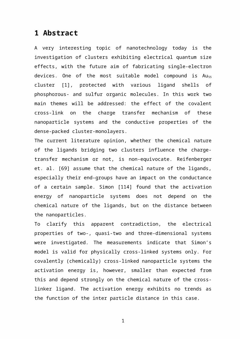
1 Abstract
A very interesting topic of nanotechnology today is the investigation of clusters exhibiting
electrical quantum size effects, with the future aim of fabricating single-electron devices.
One of the most suitable model compound is Au55 cluster [1], protected with various ligand
shells of phosphorous- and sulfur organic molecules. In this work two main themes will be
addressed: the effect of the covalent cross-link on the charge transfer mechanism of these
nanoparticle systems and the conductive properties of the dense-packed cluster-monolay-
ers.
The current literature opinion, whether the chemical nature of the ligands bridging two
clusters influence the charge-transfer mechanism or not, is non-equivocate. Reifenberger
et. al. [69] assume that the chemical nature of the ligands, especially their end-groups have
an impact on the conductance of a certain sample. Simon [114] found that the activation
energy of nanoparticle systems does not depend on the chemical nature of the ligands, but
on the distance between the nanoparticles.
To clarify this apparent contradiction, the electrical properties of two-, quasi-two and
three-dimensional systems were investigated. The measurements indicate that Simon’s
model is valid for physically cross-linked systems only. For covalently (chemically) cross-
linked nanoparticle systems the activation energy is, however, smaller than expected from
this and depend strongly on the chemical nature of the cross-linker ligand. The activation
energy exhibits no trends as the function of the inter particle distance in this case.
In the last part of this work the electrical properties of cluster monolayers are presented.
For the measurements Si substrates were used, equipped with tungsten contact structures
by electron beam lithography. In order to get an electrically insulating layer under the elec-
trical contacts, the top of the sample was oxidized to SiO2. It could be shown that a
nanoparticle system on this substrate can be activated by an exposition to a low energy
electron beam. We explain this phenomenon with trapping of excess electrons in the SiO2
layer, which induce image charges of opposite charge in the cluster layer. This effect
causes changes in the electron-configuration and perhaps also in the structure of the ar-
rangement. Asymmetrical spatial exposition of the layer leads to asymmetrical I-V charac-
1
teristics. This phenomenon can be explained similar to the rectifying behavior of the semi-
conductor diode: the arising image charges acts as electron holes in the layer.
2
2 Introduction and literature overview
The fabrication of the first transistor by Shockley, Brattain and Bardeen about 50 years ago
is arguably the most important technological development of the 20th century [2]. There is
almost no area of our life, on which transistors do not have significant impact. They are
medical and chemical sensors, parts of countless medicinal equipments, but they are also
parts of our mobile phones, CD players, or television. The greatest triumph of the transistor
is the personal computer, which now possesses more memory in the space of a small brief-
case, than computers that once filled large rooms. The above examples were made possible
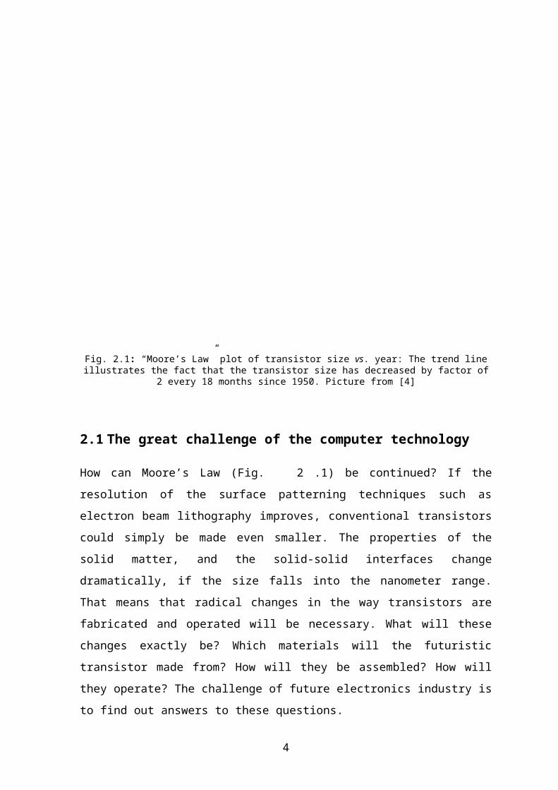
because the transistor has shrunk incredibly in dimensions over the past 50 years (Fig. 2.1).
The size of the transistor has decreased by a factor two every 18 months. This trend was
pointed out by Gordon Moore in the 1960s (Moore’s Law), and one that continues to-
day[3]. Nowadays, electronic devices employed in state-of-the-art integrated circuitry have
dimensions of the order of 300 nm.
Nowadays the big challenge of the computer technology is to be able to continue this trend.
Fig. 2.1: “Moore’s Law” plot of transistor size vs. year: The trend line illustrates the fact that the transistor size has decreased by factor of 2 every 18 months since 1950. Picture from [4]
3
2.1 The great challenge of the computer technology
How can Moore’s Law (Fig. 2.1) be continued? If the resolution of the surface patterning
techniques such as electron beam lithography improves, conventional transistors could
simply be made even smaller. The properties of the solid matter, and the solid-solid inter-
faces change dramatically, if the size falls into the nanometer range. That means that radi-
cal changes in the way transistors are fabricated and operated will be necessary. What will
these changes exactly be? Which materials will the futuristic transistor made from? How
will they be assembled? How will they operate? The challenge of future electronics indus-
try is to find out answers to these questions.
Many schemes for building nanometer-scale computer components have been proposed
[5]. These include logic based on single molecules [6], molecular shuttles, resonant tunnel-
ing diodes and atomic relays. Of all the designs, proposed for the use in future integrated
circuitry, the one receiving the most attention is perhaps the single electron transistor
(SET).
2.2 Single electron tunneling (SET) effect, and the single electron tran-
sistor (SET)*
The first signs to the SET were observed by C. J. Gorter in 1951 [7]. He investigated the
hopping conductivity in granular films. The activation energy extracted from the tempera-
ture-dependence of the conductivity was associated with the charging of individual grains
composing the film. The first clear demonstration was made by Giaver and Zeller [8], [9].
They studied the vertical tunneling through a layer of Sn grains, coated by a thin insulator
film, and sandwiched between Al electrodes. The I-V characteristics of the junction both
with and without magnetic field were measured. That allowed to exclude superconductivity
as a source of nonlinearity, and to associate the observed finite-bias offset in the I-V curve
with the effect of the charging. The authors [8], [9] have realized, that at low temperatures
electrons must tunnel through a grain one by one. A single additional electron localized on
* Both the single electron tunneling effect, and the single electron transistor will be denoted with the same ab-
breviation: SET in the text. In the non-definite cases the whole name will be written.
4
the grain in the course of tunneling, raises the potential of the grain. This prevents other
electrons from hopping onto the grain, before that electron has finished its path between
the leads, and the grain is discharged.
A single electron transistor consists of two electrodes (source and drain) and between these
a small metal or semiconductor island, which is isolated from the electrodes by some insu-
lator. The system must obey very small capacitance (typically. 10-18 F). The central island
is capacitively coupled with a third electrode, the gate electrode, which helps to change the
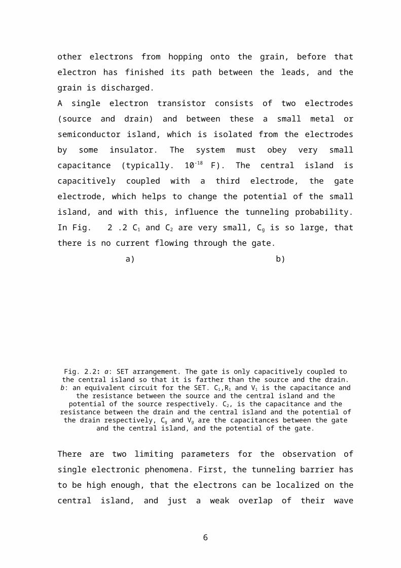
potential of the small island, and with this, influence the tunneling probability. In Fig. 2.2
C1 and C2 are very small, Cg is so large, that there is no current flowing through the gate.
a) b)
Fig. 2.2: a: SET arrangement. The gate is only capacitively coupled to the central island so that it is farther than the source and the drain. b: an equivalent circuit for the SET. C1,R1 and V1 is the capacitance and the re-sistance between the source and the central island and the potential of the source respectively. C2, is the ca-pacitance and the resistance between the drain and the central island and the potential of the drain respec-tively, Cg and Vg are the capacitances between the gate and the central island, and the potential of the gate.
There are two limiting parameters for the observation of single electronic phenomena.
First, the tunneling barrier has to be high enough, that the electrons can be localized on the
central island, and just a weak overlap of their wave functions occur outside the island. Us-
ing the tunneling resistance (RT) as a characteristic parameter of the tunneling barrier, it
can be pronounced that RT has to exceed the quantum resistance (RQ) [10] (Eq. 2.1).
2.1
where h is the Planck constant, and e is the charge of the electron.
5
An other limiting parameter is the characteristic thermal energy: it should not be higher
than the energy required for the capacitive charging of the island. In the other case the
thermal exciting of the electron is enough to charge the central island:
2.2
where kB is the Boltzman constant, and T is the temperature.
One possible solution to reach these conditions is the use of small metal or semiconductor
islands. For a small metallic particle the capacitance can be approximated by
2.3
where d is the diameter of the cluster, is the dielectric constant of the insulating medium
between the islands.
The second limiting condition is realizable with decreasing either the temperature or the
size of the clusters. For the investigation of the room temperature SET, particles smaller
than 2 nm are needed.
2.3 Arrangements of different metal clusters
The need for room temperature SET and other applications means the need of new materi-
als. The appearance of several types of nanoparticles showed that they have a wide range
use like electronic circuit elements, gas sensors, light emitting diodes [11], and catalysis.
In the literature nanoparticles mean usually metal or semiconductor particles in the range
of 1-100 nm. In this work the word nanoparticle will be used mainly for metal particles
smaller than 20 nm, since for electrical applications particles smaller then 10 nm are the
most interesting. The word “cluster” usually means a smaller particle, than “colloid”. An-
other difference between cluster and colloid refer to their size: clusters always are written
with a strict stoichiometry, as for instance Au55(PPh3)12Cl6 whereas colloids exhibit a size
distribution. In this work, clusters and colloids will be used more or less as synonyms.
6
2.3.1 Synthesis of clusters, and colloids
There are five general chemical synthetic methods to prepare clusters in the size range of
1-100 nm. These are: 1. transition metal salt reduction, 2. thermal decomposition and pho-
tochemical methods, 3. ligand reduction and displacement from organometallics, 4. metal
vapor synthesis, and 5. the use of electrochemical methods. The first, third and fifth
method are proven to give isolated transition metal clusters. It is also possible to prepare
colloids in constrained environments, like micelles, or inside porous materials, like zeo-
lites. Of course, there are also some physical methods for preparing nanoparticles. Gas
phase syntheses of metal clusters are used to generate so-called naked clusters (clusters
without a ligand shell). As they are highly reactive and tend to aggregate if they have a
physical contact, they can be studied in gas phase, or on a substrate, (see for example [12],
[13], [14] and [15]). The main strategies for gas-phase preparations are: homogeneous nu-
cleation in the gas phase, laser ablation of solids and the use of electrospray systems [11].
In the following sections all these methods will be described in detail.
2.3.1.1 Chemical methods
a) Transition metal salt reduction
The reduction of transition metal salts in solution is the most widely applied method of
generating nanoparticles of metals. For this type of synthesis four different chemicals are
needed, for four different functions. These are:
1) a transition metal salt as a precursor,
2) a suitable solvent as a reaction medium,
3) a reducing agent to generate the colloids from the metals salts,
4) a stabilizing molecule to form a protecting ligand shell around the metal core.
The same molecule can play one or two of the above functions
The function of the four entities mentioned before will be exemplified on the synthesis of
Pd~561(phenantroline)~60(OAc)~180. This cluster is formed in two steps. The first one is the
reduction of palladium(II) acetate (component 1) by hydrogen (component 3) in acetic acid
(component 2), in the presence of 1,10 phenantroline (Phen, component 4.). The workup of
7
this cluster in air leads to the uptake of O2 in 20 min with formation of air stable particles
in a good yield.
The most common particles for the investigations of SET devices are made of gold.
Among the many reasons for this, one of the most important is that they are easy to synthe-
size to characterize and air stable. Several well-elaborated methods are currently in use.
Faraday [18] was the first to synthesize nanoparticles of gold during the 18th century by re-
duction of an aqueous solution of [AuCl4]¯ with phosphorus vapor. Later Turkevitch and
co-workers reproduced this and many other syntheses [20] for the preparation of gold
nanoparticles. The 20 nm gold sol, prepared by the reduction of [AuCl4]¯ with sodium cit-
rate has become standard for histological staining applications. This reaction involves two
steps and the rate determining is the first one (eq 2.5).
2.5
This preparation can also be used for the synthesis of other metal colloids, like platinum
[21], [22], [23]. Different reducing agents like formiate, acetone-dicarboxylate, and various
pH values were also used and they have given good control on the particle size [24].
Many other techniques are used to prepare size selective colloids from metal salts. One of
the most famous is the synthesis of thiol capped gold colloids realized by Brust [25][26].
For size selective nanoparticles, a two-phase method is used. Hydrogen tetrachloroaurate
was dissolved in water, and tetraoctylammonium bromide in toluene. The two-phase mix-
ture was vigorously stirred until the tetrachloroaurate was transferred into the organic
layer. After the full phase transfer reaction, dodecanethiol was added to the organic phase,
and the aqueous solution was changed to an aqueous solution of sodium borohydride. The
electron source is the aqueous solution of the NaBH4 (see e.g. [27]).
8
b) Thermal decomposition and photochemical methods
Some organometallic compounds of the transition metals thermally decompose to their re-
spective metals under relatively mild conditions, hence providing a rich source of colloidal
metal precursors [28] [29].
The organometallic precursor can be also destroyed photochemically. Two methods can be
used: photolysis of photolabile metal complex, or reduction of the metal salts by radiolyti-
cally produced reducing agents, like solvated electrons and free radicals. The photolysis of
photographic images from silver halide emulsions have an extensive literature, and great
practical relevance. Lately a wide range of other colloidal metals has also been prepared by
this method [1].
Radiolytic methods differ in the type of reducing species, formed under irradiation, as
function of solvent and any added solute. The radiolysis of aqueous solutions of metal ions
produces solvated electrons which may either react with the dissolved metal ions directly,
or with other solutes to produce secondary radicals, which then reduce the metal cations
[30], [31].
c) Ligand reduction and displacement from organometallics
Reduction to metal can be carried out prior to colloid preparation whereby a zerovalent
metal complex is the immediate colloid precursor. Thermolysis of metal carbonyls in clus-
ter synthesis is an example for this approach. Further, the ligands can be changed to these,
which produce weak complexes, and during the nanoparticle preparation they can be re-
moved through sonication or ligand reduction [32], [33], [34],[35].
d) Metal vapor synthesis
Conceptually, but not practically, the simplest method to prepare colloidal metals is the co-
condesation of atomic metal vapor into a dispersing medium. Since the activation energy
for agglomeration of metal atoms is very low, the possibility for competing molecular
9
complex formation processes which have higher activation energies can be minimized by
operating at low temperatures
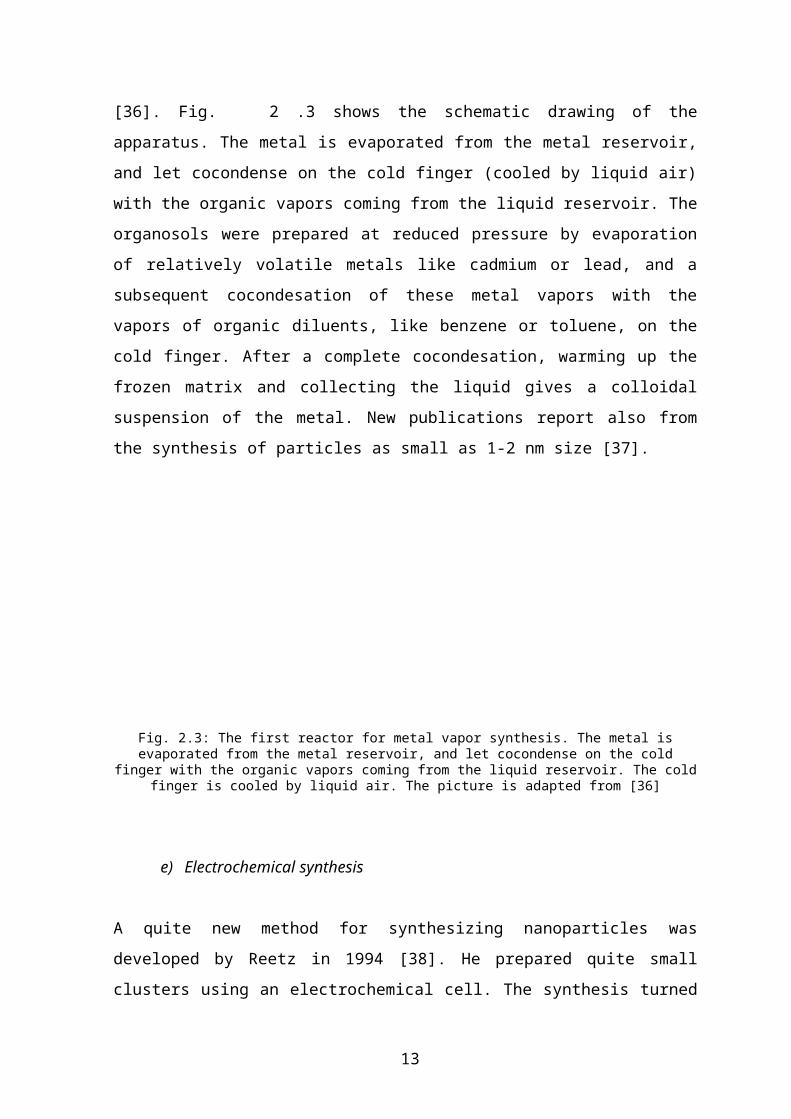
The first successful nanoparticles synthesis using this method was elaborated by Roginsky
and Schalnikoff in 1927 [36]. Fig. 2.3 shows the schematic drawing of the apparatus. The
metal is evaporated from the metal reservoir, and let cocondense on the cold finger (cooled
by liquid air) with the organic vapors coming from the liquid reservoir. The organosols
were prepared at reduced pressure by evaporation of relatively volatile metals like cad-
mium or lead, and a subsequent cocondesation of these metal vapors with the vapors of or-
ganic diluents, like benzene or toluene, on the cold finger. After a complete cocondesation,
warming up the frozen matrix and collecting the liquid gives a colloidal suspension of the
metal. New publications report also from the synthesis of particles as small as 1-2 nm size
[37].
Fig. 2.3: The first reactor for metal vapor synthesis. The metal is evaporated from the metal reservoir, and let cocondense on the cold finger with the organic vapors coming from the liquid reservoir. The cold finger is
cooled by liquid air. The picture is adapted from [36]
e) Electrochemical synthesis
A quite new method for synthesizing nanoparticles was developed by Reetz in 1994 [38].
He prepared quite small clusters using an electrochemical cell. The synthesis turned out to
be a large-scale and size selective method, and the products are redissolvable in organic
solvents.
10
2.3.1.2 Preparations of colloidal metals in constrained environment
a) Micelles and Vesicles
The reduction of physically constrained metal precursors offers the potential for restricting
the growth of the metal particles either by limiting the amount of metal particle precursor
accessible to a growing nucleus, or by restricting the motion of the precursor species and
the growing nuclei, thus diminishing the rate of productive collisions. Using this approach,
colloidal metals have been prepared in micelles or vesicles, which act as microreactors for
the preparations, and also stabilize the growing colloid.
For example, aqueous suspensions of surfactant micelles were shown to be effective in sta-
bilizing colloidal platinum, produced either photochemically or chemically (by reduction
of H2PtCl6 with H2 [39]).
b) Porous materials
Nanoparticles can also be prepared and stabilized in the confinement of porous solids with
well-defined pore or channel structures. Both semiconductor (PbS, CdS, CdSe) and metals
(Pt, Pd, Ag) can be synthesized with this method, inside molecular sieves like zeolites [40].
The clusters can grow due an ion-exchange reaction, or with the use of organometallic pre-
cursors, like metal carbonyls, as it is written in chapter 2.3.1.1b).
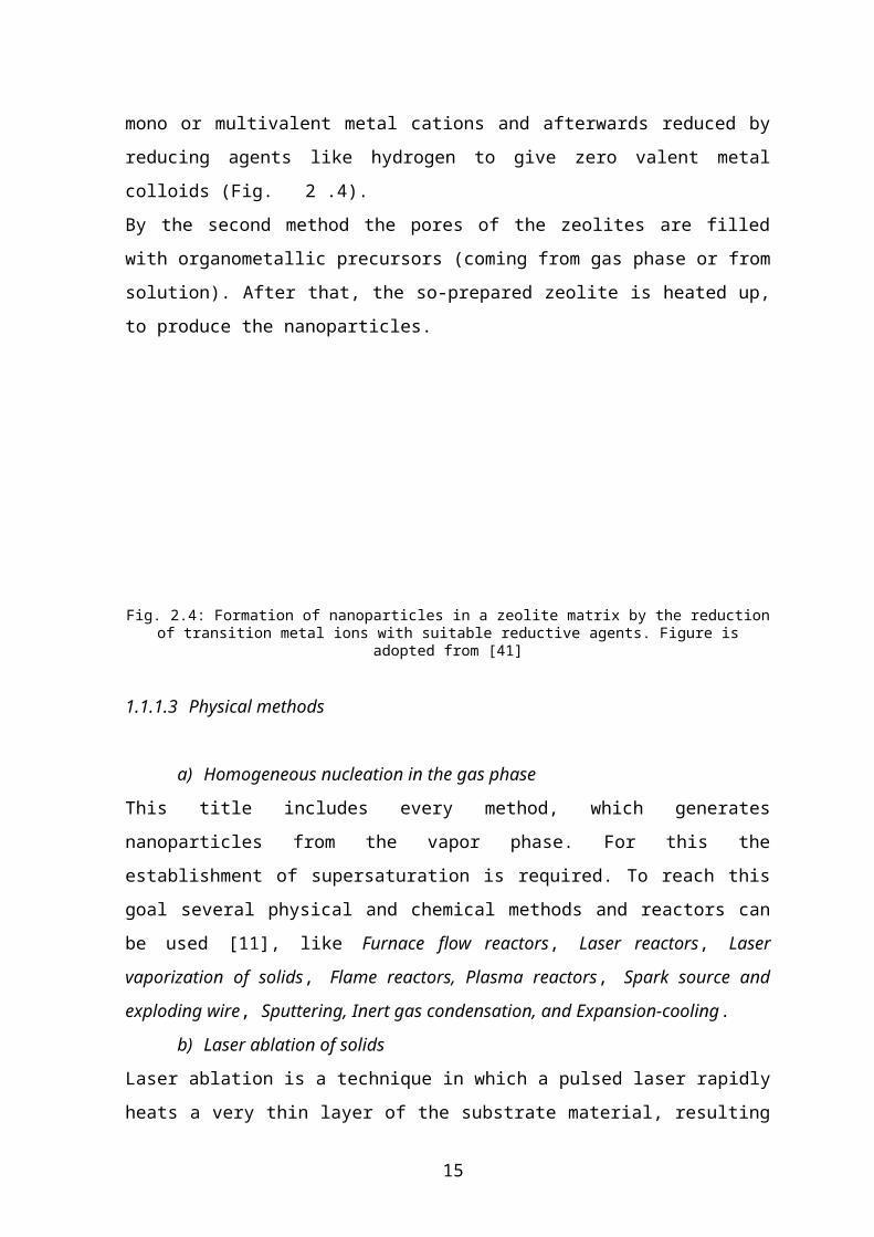
The first method uses the ion-exchange property of the zeolite. That means, that mobile
Na+ ions can be changed to mono or multivalent metal cations and afterwards reduced by
reducing agents like hydrogen to give zero valent metal colloids (Fig. 2.4).
By the second method the pores of the zeolites are filled with organometallic precursors
(coming from gas phase or from solution). After that, the so-prepared zeolite is heated up,
to produce the nanoparticles.
11
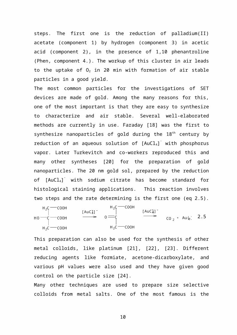
Fig. 2.4: Formation of nanoparticles in a zeolite matrix by the reduction of transition metal ions with suitable reductive agents. Figure is adopted from [41]
2.3.1.3 Physical methods
a) Homogeneous nucleation in the gas phase
This title includes every method, which generates nanoparticles from the vapor phase. For
this the establishment of supersaturation is required. To reach this goal several physical
and chemical methods and reactors can be used [11], like Furnace flow reactors, Laser re-
actors, Laser vaporization of solids, Flame reactors, Plasma reactors, Spark source and
exploding wire, Sputtering, Inert gas condensation, and Expansion-cooling.
b) Laser ablation of solids
Laser ablation is a technique in which a pulsed laser rapidly heats a very thin layer of the
substrate material, resulting in the formation of an energetic plasma above the substrate.
The pulse duration and energy determines the relative amounts of ablated atoms and parti-
cles. The non-equilibrium nature of the short-pulse (10-50 ns) laser heating enables the
synthesis of nanoparticles of materials, which normally would decompose when vaporized
directly, such as most semiconductors and multicomponent oxides do.
c) Electrospray systems
A simple way to produce nanoparticles is to evaporate micron-sized droplets of a dilute so-
lution. By choosing the appropriate solute concentration, nanosized particles consisting of
the solid residue can be obtained. For instance, drying a 1 m droplet containing a ppm so-
lution of NaCl, theoretically will yield a 10 nm NaCl particle.
12
2.3.2 Ligand exchange reactions
In the last chapter, different strategies have been presented for the cluster preparation. One
of the most important difference between clusters chemically and physically synthesized
concerned the presence or not of the ligand shell. Physically synthesized, clusters generally
have no ligand shell, thus the determined properties characterize the particles without any
disturbance. On the other hand, without molecules around them, nanoparticles cannot make
stable crystals or closed monolayers. They are air sensitive, cannot be stored and finally
their shape is changing even if they are adsorbed to surfaces. They could not be isolated, so
the most of the chemical properties cannot be determined. The clusters prepared with
chemical methods are surrounded therefore with protecting ligands. Of course the exis-
tence of non-colloidal molecules disturbs the “purity” of the system, on the other hand the
particles synthesized with this method can be isolated and investigated with chemical
methods. The diversity of the ligands, which can be used in the synthesis, is relatively
poor, for example in the case of gold particles citrate, one can use phenantroline deriva-
tives, phosphine derivatives, thiols and polymers. Multidentate molecules, for instance,
cannot be used, especially if both function groups have an affinity to the material of the
nanoparticle. The chemical properties of the nanoparticles depend on the chemical nature
of the ligands, and in certain cases a change of the ligand shell involves the formation of
materials with completely different properties.
2.3.2.1 How to add a ligand shell
In the literature, some methods to cover clusters synthesized with physical methods are de-
scribed. Most of them start with the deposition of the cluster onto a substrate and after dip-
ping the cluster into a solution, containing the protecting molecule. This technique is used
mostly for multilayer synthesis on various substrates.
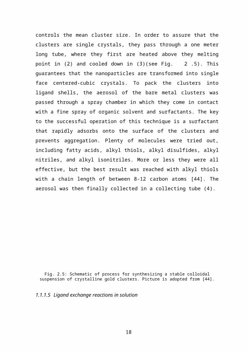
An interesting method for synthesizing thiol capped gold nanoparticles is a mixed physico-
chemical method [42] [43] [44]. The gold atoms are evaporated in a carbon crucible, in a
resistively heated carbon tube (Fig. 2.5), are entrained in He and induced to condense into
nanoclusters by mixing the hot flow from the oven with a room temperature stream of He
13

(see 2.3.1.3 a) oven methods). Controlling the conditions of the oven and the flow down-
stream in (1) from the oven, controls the mean cluster size. In order to assure that the clus-
ters are single crystals, they pass through a one meter long tube, where they first are heated
above they melting point in (2) and cooled down in (3)(see Fig. 2.5). This guarantees that
the nanoparticles are transformed into single face centered-cubic crystals. To pack the clus-
ters into ligand shells, the aerosol of the bare metal clusters was passed through a spray
chamber in which they come in contact with a fine spray of organic solvent and surfac-
tants. The key to the successful operation of this technique is a surfactant that rapidly ad-
sorbs onto the surface of the clusters and prevents aggregation. Plenty of molecules were
tried out, including fatty acids, alkyl thiols, alkyl disulfides, alkyl nitriles, and alkyl isoni-
triles. More or less they were all effective, but the best result was reached with alkyl thiols
with a chain length of between 8-12 carbon atoms [44]. The aerosol was then finally col-
lected in a collecting tube (4).
Fig. 2.5: Schematic of process for synthesizing a stable colloidal suspension of crystalline gold clusters. Pic-ture is adopted from [44].
2.3.2.2 Ligand exchange reactions in solution
The clusters can be protected with many types of ligands. As already mentioned, only a
few of them can be used directly in the synthesis. These can be, however, later exchanged
to other ones. Certain ligand phosphines or the most polymers make a weak bond with the
metal core, while others make strong bonds, like the thiol-gold bond, or the thiol-CdS core
bond.
14
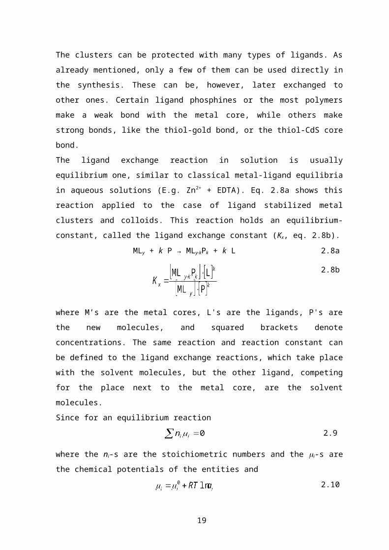
The ligand exchange reaction in solution is usually equilibrium one, similar to classical
metal-ligand equilibria in aqueous solutions (E.g. Zn2+ + EDTA). Eq. 2.8a shows this reac-
tion applied to the case of ligand stabilized metal clusters and colloids. This reaction holds
an equilibrium-constant, called the ligand exchange constant (Kx, eq. 2.8b).
MLy + k P → MLy-kPk + k L 2.8a
2.8b
where M’s are the metal cores, L's are the ligands, P's are the new molecules, and squared
brackets denote concentrations. The same reaction and reaction constant can be defined to
the ligand exchange reactions, which take place with the solvent molecules, but the other
ligand, competing for the place next to the metal core, are the solvent molecules.
Since for an equilibrium reaction
2.9
where the ni-s are the stoichiometric numbers and the i-s are the chemical potentials of the
entities and
2.10
where i0-s are the standard values of the chemical potentials, R is the gas constant, T is the
temperature and ai-s are the activity of the molecules, which are in the case of diluted solu-
tions (which is the case in almost every synthesis with this clusters), and for not charged
molecules are equal to concentrations, Kx can be written as:
2.11
Since
2.12
where p is the pressure,
2.13
15

where Gr0 is the free enthalpy exchange of the whole reaction. Gr
0 is the difference of
the Gibbs-energies of the destroyed and the developed bonds. Entropy changes can usually
be neglected, because there are the same number of molecules on the two sides of the two
sides of the reaction equation.
2.14
where HbP is the bond enthalpy between the metal core and the new molecules and Hb
L is
the bond enthalpy between the metal core and the ligands.
2.13
That means that, if the metal core – ligand bond is weak, but the metal core-new molecule
bond is strong, than GrP has a very large and Gr
L a smaller negative value. Kx is large, so
practically all of the ligands will be exchanged to the new molecules. On the other hand, in
an opposite case, the ligand-new molecule exchange practically does not take place.
There are mainly two strategies for exchanging the ligands in a homogeneous reaction. The
first is to transfer the colloids from a weaker bonded ligand shell to a stronger bonded, like
exchanging phosphines, polymers or citrate to thiols. These reactions are usually fast, and
with yields of 80% to 100% (Kx is large). The second is based on the exchange of two
types of molecules with same bond strength, like thiols to thiols, or thiols to dithiols. The
yields of these slow reactions (between 40% and 60%) depend on the steric and other prop-
erties of the molecules (Kx is close to 1).
A huge number of examples for all the strategies can be found in the literature. In this sec-
tion an overview of the techniques and results obtained with gold clusters will be pre-
sented.
Ligands like phosphines, citrate, or different polymers are easily removable, and substi-
tutable by thiol ligands [46] [48] [45]. Tannic acid stabilized gold sols can be turned to
thiol stabilized simply by adding thiol to the solution, and remove the free tannic acid with
dialysis [45]. Citrate stabilized gold sols can be cross-linked with propanedithiol, with sim-
ply adding the new ligand, and let the nanoparticle-polymer precipitate [48]. In Ref. [46]
16
gold particles were transferred from an aqueous phase to the organic phase, using toluene
soluble thiols.
A more spread out technique is to synthesize the clusters with thiol ligands. This is practi-
cally more advantageous, because they are more stable in solution, but they are not as
much available for clear ligand exchange reactions. The non-stoichiometric exchange of
the ligands sometimes causes problems, because the used material is not chemically pure.
On the other hand many measurements can be imagined (and were done), to determine the
exact number of the exchanged ligands. In Ref. [47] octhanethiol molecules was ex-
changed to -ferrocenyloctanethiol molecules, to study the electrochemical properties of
the as-synthesized particle. By a simple measure of the area under the voltammetric curve,
the authors were able to determine the number of ligands exchanged.
It is also possible to investigate the ligand exchange reactions by kinetic measurements
[63]. In the case of thiol-to-thiol exchange, Murray [63] found that the speed of the ligand
exchange reactions depends on the concentration of the ligands and the nanoparticle. They
also suggest a mechanism. According to this, a thiol molecule enters into the ligand shell
of the molecule and protonates the bound thiolate. In the second step the protonated mole-
cule leaves the cluster. They also assume that the molecules on the terraces of the clusters
form stronger bonds with the metal core than those on the edges and corners.
2.3.2.3 Ligand exchange reactions on the surface (preparation of mono-and multilayers)
The ligand exchange reactions can also take place through a specific adsorption step. That
means that first the surface is functionalised, using a functional group able to create a
strong specific interaction with the metal core. After this the nanoparticles are adsorbed.
During the second step, an exchange between a part of the ligand shell and the function
group of the ligands on the surface takes place. This phenomenon can be supported by the
solvent. This method can be used to synthesize monolayers like in [55], [57], [59], and
[60], as well as multilayers [56], [58]. It is also possible to use the Langmuir-Blodgett tech-
nique in order to create two dimensional cross-linked nanoparticles assemblies [61], [62].
This strategy doesn’t contain an adsorption step, the ligand exchange happening in a homo-
17
geneous reaction on a water surface. In the following it will be focused mainly on the lig-
and exchange reactions of gold nanoparticles.
The easiest strategy to obtain closed monolayers of clusters is obviously to exchange a
weak bonded ligand to a strong bonded function group, like phosphine to thiol[55]. Partial
change of thiols to dithiols is also possible[59], [60], but the reaction is very slow and not
stoichiometric.
In Ref. [55] a SET was prepared using phosphine stabilized gold colloids and a thiol func-
tionalised surface. Gold nanoelectrodes were prepared with Electron Beam Lithography
(EBL), then functionalised with hexanedithiol. Particles, bigger in diameter, than the space
between the electrodes, were let to adsorb onto the surface. The particles partly loose their
ligands and adsorb between the two electrodes onto the surface, making a link between the
two contacts (see Fig. 2.6).
A very interesting use of the ligand exchange reactions is the light lithography with
nanoparticles [58]. A light sensitive molecule is bonded to the surface, and with the use of
a mask, some parts are destroyed, others not. On the destroyed part an amino-function-
alised surface is gained from the original molecules. Dodecylamine stabilized gold parti-
cles are adsorbed to the surface so that their metal core anchored to the free amino groups
on the surface. To get a multilayer of the clusters, the sample was dipped into a dithiol so-
lution and back to the gold sol. These steps are repeated several times, to get a real mi-
crostructure on the surface. (For details see [58].)
The ligand exchange reaction from thiol to dithiol is a very slow reaction, so the adsorption
of the thiol capped molecules with a thiol functionalised surface is very slow. The reaction
time can be up to 1 week as reported in Ref. [51], [59] and [60]. To fasten the reaction it is
easier to start with partially functionalised particles and to anchor them onto the gold sub-
strate like in Ref. [59].
The ligand exchange reactions are commonly used techniques for the preparation of many
types of cluster arrangements.
18
2.3.3 Preparation and properties of zero-, one -, two–, quasi-two-, and three-dimen-
sional arrays of metal clusters
Arrangements of different particles from many kinds of metals and semiconductors are dis-
cussed in the literature. Mainly two strategies are followed in the publications which
mostly differ in the strength of the bonds in the array. One type of these methods are the
“physical methods”, where there is just a weak bond, or no bond between the particles, the
others are the “chemical methods” which build up the array with strong covalent or ionic
bonds.
In the following chapters the different types of arrangements will be introduced.
2.3.3.1. Zero-dimensional “arrangements”
A zero-dimensional “array” is represented by one nanoparticle on a surface. There are es-
sentially two methods to get information about the properties of one single cluster. The
first, and the most spread out technique is the use of STM. A submonolayer of nanoparti -
cles is deposited onto a surface, with physical or chemicals methods [66][67][68][69] and
an STM tip is positioned over it. This technique is used mostly for electrical measure-
ments, but it can be also used to determinate the size of the clusters. A very interesting as-
pect of this method is, that the size of the monolayer-coated particles seems to be as big as
the diameter of the cluster and the ligand shell together (see e.g. [67]). This means that the
effect of the covering molecules cannot be avoided by the models built up for the charge
transfer mechanisms, since the electrons tunnel through the protecting molecules.
The second method for the zero-dimensional measurements is, to capture the nanoparticles
between two electrodes [55][70][71][72][73]. The distance between the two-electrode sys-
tems fabricated must be smaller than the diameter of the studied cluster. To reach this goal,
EBL is used to get electrode systems with distances of 20-50 nm between the metal con-
tacts. To obtain even smaller gaps between the nanocontacts, some metal is evaporated
onto the surface (Fig. 2.6). With this help electrode distances between 10 and 20 nm can be
reached. The particles can be captured as well by specific chemical bonds [55][71], as with
19
electrophoretic effects from solutions[72], or simply moving them on the substrate with an
AFM tip[70][73].
Fig. 2.6: Nanocontacts prepared by EBL. AFM measurements are made during the manipulation of 50 nm gold particles. Figure is adapted from[73].
2.3.3.2. One-dimensional arrangements
An ideal one-dimensional arrangement is a row of clusters. This structure is difficult to ob-
tain, so in the literature mainly quasi-one-dimensional structures are presented. That
means, that instead of one single row of clusters a thin wire is fabricated, with a width of
some hundreds of nanometers.
There is no commonly used strategy to fabricate nanowires. The difficulty is; how to create
chemically or physically different regions on a substrate in order to avoid a two-dimen-
sional particles assembly on the entire surface.
The easiest way to fabricate chains of clusters is to crystallize the nanoparticles slowly on a
surface, and stop the process in an early stage, when there are mainly one-dimensional
structures [79].
20
Small chains of nanoparticles are obtainable also by stepwise chemical methods [57].
Longer chains of bigger colloids can be prepared by the reduction of metal salt onto a
DNA template [78].
Quasi-one-dimensional structures can also be obtained using Langmuir-Blodgett (LB)
technique [74], [75]. One possibility is to prepare a low-density LB film [74]; the other is
to break the closed LB layer during the transfer to the substrate, with the use of high trans-
fer speed. Chi and coworkers broke the LB layer of a fatty acid, using the periodic move of
the meniscus at high transfer speeds, and filled the obtained channels with gold clusters
[75].
Selective adsorption techniques are commonly used to fabricate nanowires. Building spe-
cific bonds between clusters and biomolecule templates is just one of the possibilities[77].
With an oxidation process, a certain part of a passive surface can be activated. So, spacer
molecules can selective by adsorb onto it. Nanoparticles can adsorb to the spacers, but not
on the passive part of the substrate. That means, that with the use of a conducting AFM tip,
which is able to oxidize, nanowires can be fabricated [80] (Fig. 2.7).
a)
b)
21

Fig. 2.7: Preparation of nanowires with nanooxidation method. Figures adapted from [80]
An interesting approach to prepare nanowires is to fill Al2O3 pores with the nanoparticles
[65], [64],[76],[77].
2.3.3.3. Two-dimensional arrangements
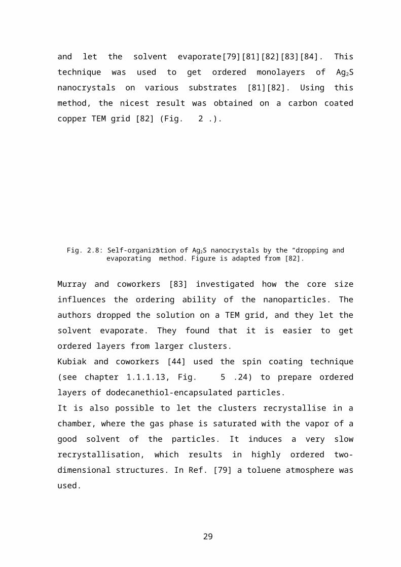
The easiest method to prepare monolayers of nanoparticles is to dispose a drop of the clus-
ter solution onto a substrate, and let the solvent evaporate[79][81][82][83][84]. This tech-
nique was used to get ordered monolayers of Ag2S nanocrystals on various substrates [81]
[82]. Using this method, the nicest result was obtained on a carbon coated copper TEM
grid [82] (Fig. 2.).
Fig. 2.8: Self-organization of Ag2S nanocrystals by the “dropping and evaporating” method. Figure is adapted from [82].
22

Murray and coworkers [83] investigated how the core size influences the ordering ability
of the nanoparticles. The authors dropped the solution on a TEM grid, and they let the sol-
vent evaporate. They found that it is easier to get ordered layers from larger clusters.
Kubiak and coworkers [44] used the spin coating technique (see chapter 2.4.5.4, Fig. 5.24)
to prepare ordered layers of dodecanethiol-encapsulated particles.
It is also possible to let the clusters recrystallise in a chamber, where the gas phase is satu-
rated with the vapor of a good solvent of the particles. It induces a very slow recrystallisa-
tion, which results in highly ordered two-dimensional structures. In Ref. [79] a toluene at-
mosphere was used.
LB technique is a common used method for the fabrication of ordered monolayers. It is
proved to result mainly in hexagonal lattices in the case of nanoparticles [61][85][86][87].
Mayya and Sastry [88] were able to immobilize a monolayer of gold clusters on the
toluene-water interface. The aqueous solution of carboxytiophenol-capped particles was
brought in contact with a toluene solution of octadecylamine. After vigorous stirring, the
clusters were transferred to the interface and the wall of the glass container [88]. The thick-
ness of the layer on the glass indicated that a monolayer formed.
Nanoparticle adsorption onto a modified surface, using the fact that most type of the clus-
ters easily self-assemble, is the most spread-out technique for monolayer preparation (see
E.g. [51][59][89][90][91][92]). The chemisorption happens mainly through ligand ex-
change reactions. Weak bonded ligands can be changed to stronger bonded ones [89][92],
or in the case of equal strong bonds with slow ligand exchange reactions [51][59][90][91].
It is also possible to get two-dimensional arrays with the use of AFM [93]. In this article
the authors manipulate the single particles with an AFM tip, to get structures consisting of
5-10 clusters.
An interesting strategy to get highly ordered arrangements of naked particles at large dis-
tances, is the preparation through the self-assembling of micelles [94]. The particles encap-
sulated in a surfactant micelle are let to adsorb to a surface. After this step trough a treat-
ment with oxygen plasma, the walls of the micelles are burned away, so single naked clus-
ters remaining on the substrate. The distance of the clusters about is 5 to 10 nm, approxi-
mately two times the thickness of the micelle.
23
2.3.3.4. Quasi-two-dimensional arrangements
Quasi-two-dimensional arrangements of nanoparticles are thin films or multilayers of clus-
ters. They can be built up using direct or step-by-step methods.
Direct preparations are the one-step fabrications like dropping a relative concentrated clus-
ter solution onto a substrate and let the solvent evaporate, or the spin coating of solutions
(see chapter 2.4.5.4 and Fig. 5.24).
An interesting thin-film preparation method is made by Zhong [53]. He synthesized a gold
cluster cross-linker polymer on a thiol-modified surface by ligand exchange reaction. This
technique is the one step-cross-linking and precipitation method. The polymer precipitated
from the solvent to the surface, resulting in a layer with relative high surface roughness
(see Fig. 2.2).
Step by step synthesis of multilayers means that after adsorption of a cluster monolayer by
a substrate a linker layer is deposited, causing once more the substrate active for the ad-
sorption of another cluster layer. These two steps are following each other, 2 to 100 times,
resulting in the formation of a thin film, with different thickness. Layers can be ionic, e.g.
polymers [95][96][97], small ionisable molecules [98][99], differently coated clusters
[100], or covalent.
The easiest method to prepare ionic bonded multilayers with polymer linkers is the use of
positively charged clusters and negatively charged polymers [96]. In this case, the film
consists of a cationic polymer coated nanoparticle system alternating with an anionic poly-
mer linker.
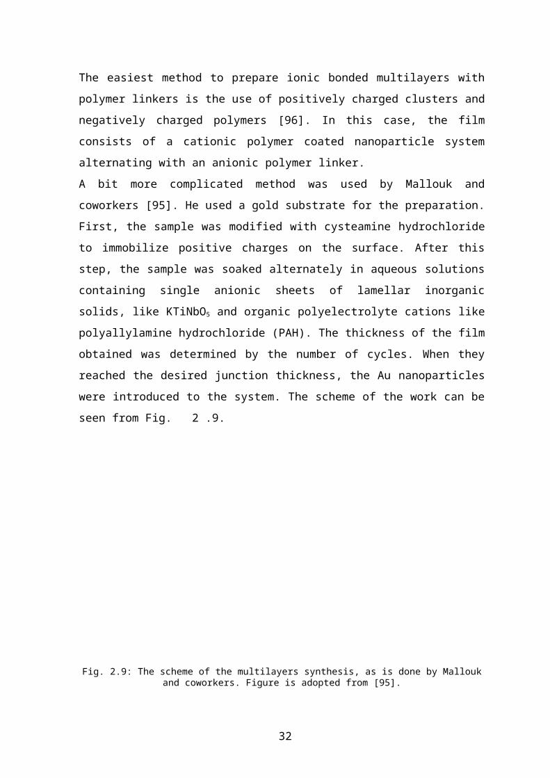
A bit more complicated method was used by Mallouk and coworkers [95]. He used a gold
substrate for the preparation. First, the sample was modified with cysteamine hydrochlo-
ride to immobilize positive charges on the surface. After this step, the sample was soaked
alternately in aqueous solutions containing single anionic sheets of lamellar inorganic
solids, like KTiNbO5 and organic polyelectrolyte cations like polyallylamine hydrochloride
(PAH). The thickness of the film obtained was determined by the number of cycles. When
24
they reached the desired junction thickness, the Au nanoparticles were introduced to the
system. The scheme of the work can be seen from Fig. 2.9.
Fig. 2.9: The scheme of the multilayers synthesis, as is done by Mallouk and coworkers. Figure is adopted from [95].
The use of small ionic molecules is also possible to prepare multilayers. In this case e.g.
bipyridinium cyclophanes [98] or benzamidines [99] can be used as linkers.
An interesting example of ionic self-assembly is described by Kumar [100]. In this work
gold and silver particles, stabilized respectively by 4-aminothiophenol and 4-carboxythio-
phenol were used. Because of a possible ionic interaction between the ligand (positively
charged of the amino group negatively charged of the carboxyl group), an alternative mul-
tilayer gold-silver was built.
The preparation of covalently bonded multilayers is similar to the ionic ones, except, that
in this case the linker bonds covalently between the layers and also the particles inside the
layer. The preparation usually happens through two-phase ligand exchange reactions. In
the case of gold particles the fabrication starts with the mercapto functionalisation of the
surface (except [58]), than altering rinsing in the gold cluster, and dithiol solution (except
[101], where the linkers are diisocyanide molecules).
An interesting preparation is presented in Ref [102], in which a composite semiconductor-
metal layer is fabricated, with altering rinsing in dithiol-CdS nanoparticle solution-dithiol-
25
Pt clusters. The change of the sequence was of course also possible, so different composite
multilayers were also obtainable.
2.3.3.5. Three-dimensional arrangements
Three-dimensional arrangements of nanoparticles are easily obtainable by crystallization of
cluster solutions. This happens actually in every synthesis of clusters, when the product is
isolated.
Crystallization can also be induced by cross-linking of colloids [53][59]. Both papers re-
port that the precipitation pf the clusters leads to a polymer, although this was not intended.
Induced crystallization of nanoparticles in toluene atmosphere is reported by Gutierrez
[79]. During the very slow rearrangement of the entities in this case, relatively big single-
crystals of nanoparticles can be obtained.
2.3.4 Preparation techniques of chemically cross-linked nanoparticle systems
2.3.4.1 Homogeneous reactions
The mixing of nanoparticles with different di-, or polyfunctional molecules having a strong
specific bond to the metal core in a solution, after shorter or longer time ligand exchange
reactions will happen (see chapter 2.3.2.2). This reaction will polymerize the system, to
lead to precipitation of the clusters.
Citrate stabilized gold colloids precipitate in the course of a half an hour after mixing them
with propanedithiol. The reaction is followed by UV-Vis spectroscopic measurements of
the solution [48]. The color changes from blood red to violet before precipitation occurs.
If thiol stabilized gold clusters are codissolved with dithiols, and in the presence of a gold
plate, as it is done in [44], [49], [50], [51], [52] and [53], it is not necessary to change all
ligands against dithiols for the precipitation, but only some of them. In Ref. [44] conju-
gated molecules were used to interconnect particles in a monolayer and the electrical prop-
erties were measured. As it is well known for the electron transport in a layer, conducting
26
paths are enough (see chapter 4.5.2)[54], so for the measured current-voltage characteris-
tics the exchange of all the ligands is not proved.
In Ref. [49] a monolayer of gold nanoparticles was prepared with codissolving the dithiols
and the thiol-stabilized clusters in a solution and dipping a pure gold plate into it. If on the
surface of a gold particle at least one of the thiols is changed to dithiol, it has the chance to
anchor down to the gold plate. If the oxidation of the dithiols is prevented, a closed mono-
layer can be gained with this technique. In Ref. [50] and [51] dithiols were codissolved
with gold particles. In Ref. [50] it is shown, that cross-linking clusters can take place, and
the resulting polymer can precipitate from the solvent, if the solution is concentrated
enough. To get thiol functions outside the entities, then it has to be worked in diluted solu-
tion [51] and the product has to be separated by liquid extraction (Fig. 2.1).
Fig. 2.1: Functionalising a gold nanoparticle with thiol groups. The strategy for preparing a monolayer with this technique is, to exchange some of the thiols by dithiols, and the so gained particle anchoring to a gold
surface. The figure is adopted from [51].
In Ref. [52] and [53] ligands are exchanged to prepare cross-linked thin films of nanoparti-
cles. The authors suggest, that this is an easy and fast technique to prepare layers of clus-
ters (Fig. 2.2). Thiol protected clusters are codissolved with dithiols in the presence of a
substrate. The cross-link is allowed and the gained polymer is precipitated from the solu-
tion onto the substrate. The thickness of the film is changing inside the layer, because the
precipitation is not homogeneous. Changing the reaction time, the average thickness of the
film can be controlled.
27
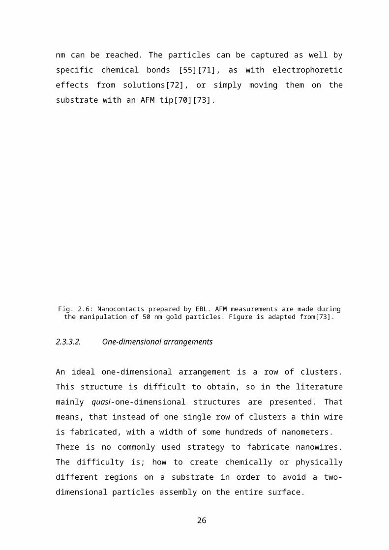
Fig. 2.2: Polymerization of nanoparticles in the presence of dithiols. Figure is adopted from [53].
In all papers dealing with dithiols, an important rule has to be pointed out. All authors
work with solvents like toluene or hexane, which are not acid-base active (except [44]),
and does not contain much water which can act as acid-base catalyst. When the proton of
the –SH group is dissociated, the dithiols can polymerize easily. For solvents like ethanol
or dichloromethane (which always contains traces of HCl as a decomposition product, and
absorbs readily the humidity) nitrogen atmosphere has to be used, to avoid this process.
2.3.4.2 Langmuir-Blodgett techniques
Chen [61] experienced that chemically cross-linked samples can be prepared on a water
surface using LB technique. She spread the cluster solution (hexanethiolate protected clus-
ters in hexane solution) onto a water surface, followed by spreading of a dithiol in CHCl3
solution. The molar ratio of the two components was approximately 1. It is observable, that
28
the solvent of the dithiol doesn’t dissolve the clusters. This is very important, because oth-
erwise microcrystals of clusters would be formed.
After spreading both component and evaporation of all solutions, the layer was compressed
for a relative high surface pressure. After waiting for 6 hours, the cross-linkage was com-
plete and the sample could transferred to the substrate. The layer proved to be a rigid and
very stable one.
2.3.4.3 Heterogeneous reactions
Every multilayer preparation technique that is based on covalent bonds between the metal
core and the ligands are covalently cross-linking the particles during the reaction [56],
[58]. (see chapters 2.3.2.3 and 2.3.3.4)
Fig. 2.3: Build up of a multilayer using tetraoctylammonium bromide stabilized gold clusters, and dithiols. Figure is adopted from [56].
In Ref. [56] a multilayer was built up with tetraoctylammonium bromide stabilized gold
particles, and dithiols. A thermally grown SiO2 layer was functionalised with thiol, using
3-(mercaptopropyl)-trimethoxysilane. After, the sample was dipped into the gold solution
to get a layer of the particles. This dipping procedure, thiol solution-gold solution, was re-
peated in order to obtain multilayers of clusters (Fig. 2.3).
In Ref. [57] also the synthesis of cross-linked particles is reported. The first step was the
immobilization of citrate stabilized particles. They adsorbed onto an amine functionalised
surface. The authors did not mention, but it could be a chemically rather complicated step,
29
because the citrate stabilized gold clusters in water solution can adsorb to an amine surface
with (electrostatic bonds), and without (covalent bond from amine to metal core) their lig-
and shell. After this step the substrate was dipped into an ethanol solution of very diluted
hexane dithiol molecules for 24 hours. The authors claim that the dithiol exchanges the sta-
bilizing citrate molecules and functionalises the surface of the clusters with thiol, so after
immersing to the gold sol again, the particles will form small chains. The Scanning Elec-
tron Microscope image of their layer before and after dithiol immersion is depicted on Fig.
2.4. It is observable, the number of the islands on the second image is smaller than on the
first one (104 particles on the first picture, and 129 on the second one). That indicates that
the dithiol solution dissolved some of the deposited gold particles, but still made an inter-
connection between them. The bond between the surface and the entities can be covalent,
but acid-base as well.
a) b)
Fig. 2.4: Citrate stabilized particles were let to adsorb in an amine functionalised surface. After this step the substrate was dipped into an ethanol solution of very diluted hexane dithiol molecules for 24 hours, and back
to the gold sol. SEM image of the layer before (a) and after dithiol (b). Figures are adopted from [57].
30
2.3.5 Electrical properties of arrays made of metal clusters
Modern microelectronics strongly tends to miniaturization of the circuit elements and to a
larger degree of integration. The shorter distances between the elements on a chip lead to
an increase in the performance speed and, therefore, to smaller delay times in the informa-
tion exchange. That is why the investigation of the electrical properties of every arrange-
ment made from metal clusters earns more and more interest in the recent years. In particu-
lar electrical studies on zero-, one-, two-, quasi-two- and tree-dimensional arrays of
nanoparticles appear to give new ideas for their possible future application.
2.3.4.1. Zero-dimensional arrangements
There are two different methods for the study of single quantum dots. The simpler, and
more spread-out technique is the Scanning Tunneling Microscopy (STM). In this case the
tip is positioned above a cluster, the height feedback is turned off and a Scanning Tunnel-
ing Spectroscopic curve (STS) is measured [15], [44], [67], [68], [69], [76], [103], [104],
[105], [131]. This means that the tunneling current is measured as a function of the sample
voltage, or the distance between the sample and the tip. The preparation of quasi-monolay-
ers needed for this technique is described in Chapter 2.3.3.1. The other techniques is the
preparation of small nanocontacts with Electron Beam Lithography (EBL), and catch a
cluster between them [55], [70], [71], [72], [106] as it is described in Chapter 2.3.3.1.
The electrical measurements show nonlinear I-V curves in case of both techniques, because
of the so-called Coulomb-blockade (in details see Chapter 4.1). The nonlinearity is en-
hanced with the smaller particle size[15], and the lowertemperature[44]. This phenomenon
is caused by the clusters, as it is proved by Reifenberger [68]. In this work he measured the
STS curve when the tip was positioned above and next to a cluster. As can be observed on
Fig. 2.5, when the tip is above a cluster, clear nonlinearity in the I-V curve is measured,
however in the other case, simple Ohmic behavior is obtained.
31
a) b)
Fig. 2.5: STS curves measured above (a), and next to (b) a cluster. Figure is adapted from [68].
The differences between the two types of measurements are the length, and the height of
the two tunneling barriers, on both sides of the metal core (Fig. 2.6). In the case of STS,
the tunneling gate can be modeled by two different resistive-capacitive electric circles (RC
circle), but in the other case the height of the two gaps is the same. Both situations are dis-
cussed by Korotkov [107] who reported that if the two tunnel barriers are really different, a
Coulomb staircase behavior can be expected in the I-V measurements [67], [105], [131],
but not in the other case [55], [70], [71], [72], [106].
a) b)
Fig. 2.6: STS arrangement (a), and cluster between two nanocontacts, fabricated with EBL (b). The height of the tunnel barrier is different in the case of a), so Coulomb staircase can be expected in the I-V curve, but the
same in b). Fig a) is adapted from [69].
32
The fine structure of the I-V curve observed in the case of a cluster between two EBL fab-
ricated nanocontacts shows the electron energy levels of the investigated cluster [55],
[106].
2.3.4.2. One-dimensional arrangements
There are very few experimental data concerning the electrical properties of one-dimen-
sional arrangements. As a main difficulty a very small disorder in the array of the cluster
row can cause big differences in the measured data [108]. Although some previous one-di-
mensional structures of metal clusters are reported on the literature (see Chapter 2.3.3.2),
the measurement of the electrical properties is still a big challenge.
Fig. 2.7: SEM image (a), and a sketch (b) of a one-dimensional array of nanoparticles between two nanocon-tacts fabricated by EBL. The picture is adapted from [57].
The only example found as a real one-dimensional experimental result was the one made
by Sato and coworkers [57]. The detailed information of the synthesis of the layer can be
read in Chapter 2.3.2.3. As it is observable in Fig. 2.7, the nanocontacts are bridged by
three clusters in a row. This is the first promising result for the preparation of a SET. The
authors measured the I-V curve of this system and found both the Coulomb-blockade, and
33
the oscillation of the source-drain current in the function of the gate voltage. This is a con-
vincing proof for a working as a SET.
2.3.4.3. Two-dimensional arrangements
The electrical behavior of the two-dimensional arrangements of bigger (d > 5 nm) particles
is metallic. That is why not many measurements were published in this diameter range yet.
Smaller particles can be investigated [44], [87], [109], [110] also with electrical methods.
The first results in this area was obtained by Andres et al. [44]. They measured the I-V
curve of a monolayer consisting of 2 nm clusters. The curve seemed to follow Ohm’s law
at room temperature and showed Coulomb-blockade at lower temperature (Fig. 2.8).
Fig. 2.8: The temperature dependence of the I-V curve of a cluster monolayer. Figure is adapted form [44].
2.3.4.4. Quasi-two- and three-dimensional arrangements
The resistance of a multilayer consisting of metal clusters with a core size bigger than 2 nm
in diameter is normally too small to be measured [111]. This is also the case in three-di-
34
mensional measurements. The results received for the two cases are comparable, that is
why they are discussed in the same chapter.
If any electric information is needed from a film, smaller colloids or longer ligands have to
be used, otherwise the resistance is too small to be measured. Murray and coworkers used
2.4 nm gold clusters with different thiols as ligands, [112], [113]. The alkyl chains varied
from 4 to 16 carbon atoms. The simple Arrhenius model as well as the so-called granular
model (see chapter 4.5.3) was fitted to the measured curves, and the activation energy was
calculated with both theories. Brust et. al. [56] showed that this systems can be better ex-
plained with the granular model. It was elaborated for the electrical properties of cermets,
and other metal-insulator composite materials (see chapter 4.5.3). According to this theory,
electrons move through the material with hopping from one metal island to another in an
insulator medium. In this case, the electrons jump from one cluster to another in an alkyl
chain medium (see chapter 4.5.3). This model fits very well with other nanoparticle sys-
tems. Simon and coworkers applied the same theory for palladium clusters [114].
2.4 The Au55 cluster*
The Au55 cluster is different from the above-mentioned nanoparticles, because it presents a
really monodisperse size. The important difference compared to the other particles resides
in the fact that the number of metal atoms as well as the ligand shell are well-defined. This
strict stoichiometrical composition means that it is a giant macromolecule, with the proper-
ties of a nanocluster. This is very important because it is known that in this size range
small changes in the composition of the particles means by differences in its properties.
Some characterizations require monodisperse particles. In the case of electrical measure-
ments, for instance, a few bigger clusters in the material induced an increase of the conduc-
tivity of the sample.
* In the following chapters the sign Au55 denotes to the metallic core consisting of 55 gold atoms, surrounded
by any ligand shell. If a particular cluster is mentioned, the name, or the sign will be always written exactly,
like Au55(PPh3)12Cl6, or Normal Au55 ( see chapter 8.1)
35

All of these characteristics make the Au55 cluster the smallest available clusters useful for
nanoelectronic investigations. Its size and electron structure gives the possibility to it as a
nanotransistor or a room temperature single electron device in the future.
2.4.1 The strategy for the synthesis of Au55 cluster
As it is explained in Chapter 2.3.1.1, many good strategies for the synthesis of metal clus-
ters exist. To prepare Au55 the transition metal salt reduction method is used [1], [116],
[117] ( for details see chapter 8.2):
AuCl(PPh3) + B2H6 → Au55(PPh3)12Cl6 2.14
In this case AuCl(PPh3) is the transition metal salt, B2H6 is the reductive agent, benzene
and toluene act as a solvent. B2H6 has a double function in this reaction: firstly, as a reduc-
tive agent it reduces the Au(I) salt, secondly, as a Lewis acid it reduces the concentration
of the PPh3 [1], and with this it assures the optimal parameters for the formation of the
clusters. The PPh3 is the stabilizing agent. As a Lewis base it coordinates to the gold atoms
in the cluster, similar to the coordination in the AuCl(PPh3) salt, except that the oxidation
number of the gold is different in the two cases.
The structure of the Au55(PPh3)12Cl6 cluster can be observed in (Fig. 2.9) [1], [116], [117].
It consist of two parts, a metallic core and an organic ligand shell. The gold core contains
55 gold atoms, which are crystallized in a cubic closed packed structure. That means, that
the shape of the central metal core is cuboctahedral, with a diameter of 1.4 nm. The or-
ganic surrounding consists of 12 triphenylphosphine molecules; they are bound to the cor-
ners of the central polyhedron. The cluster contains also 6 chlorine atoms, which are
aligned in the middle of the square sides of the cuboctahedron (Fig. 2.10) [120]. The whole
cluster is 2.1 nm in diameter.
EXAFS measurements indicated that the Au-Au distance of the clusters is 0,280 nm corre-
sponding to a slightly disordered cuboctahedral structure [127].
36

Fig. 2.9: The structure of the Au55(PPh3)12Cl6 cluster. ● Au atoms, ● P atoms, ● C atoms. The Cl and H atoms are missing from the figure.
Fig. 2.10: The structure of the Au55(PPh3)12Cl6 cluster. On the first picture the big circles represent the PPh3
ligands. On the second picture the signs show which ligand binds to which gold atom. Figure is adapted form [118]
37
2.4.2 “Magic” numbers in the cluster chemistry: specific stoichiometry of the metal
cores
Using the same strategy for the synthesis of other metal clusters it turned out that there are
some specific numbers of metal atoms, called “magic numbers”, which are more stable
than the others. These clusters, which consist of 13, 55, 147 etc. atoms, are full-shell clus-
ters (Fig. 2.11). That means that they are like nanocrystals of metal atoms, crystallized in
the closest packed structure, and the shape of the clusters are geometrically closed, which
means that they have the minimum number of surface atoms for their size. So it can be
spoken of one-shell, two-shell, and so on, clusters. In the case of metal clusters, this poly-
hedron is usually cuboctahedral. For the formation of this shapes particular number of
atoms are needed, for the nth shell (10n2 + 2). The magic numbers N of a k shell cluster can
be calculated with the formula:
2.15
Fig. 2.11: The stoichiometry, and geometry of the full shell clusters. Figure is adapted from [118].
With the kinetic investigation of these reactions the “birth of a metal” can be followed
(Fig. 2.12). It seems that the magic number clusters occupy a kind of energy minimum on
the energy diagram of this reaction. That magic number which belongs to the first step lo-
cal minimum of the curve that is deeper than the characteristic thermal energy in a certain
reaction, depends on the synthesis parameters like temperature, the concentration of the so-
lution, the reductive agent and the chemical nature of the ligand together with the metal. In
the case of gold and PPh3 the formed metal core consists of 55 gold atoms, by palladium
and phenantroline it consists of 561.
38
Fig. 2.12: The energetic curve of the birth of the metal. The images of the clusters are the same as on (Fig.2.11).
2.4.3 The physical-chemical properties of the Au55 cluster
Because of its ligand shell, the so synthesized cluster is soluble in many organic solvents,
especially in dichloromethane. The solutions are usually brown, depending on its concen-
tration it can change from light brown (diluted solutions) to dark brown (concentrated solu-
tions).
The UV-Vis spectra of cluster solutions do not show a plasmon resonance in the range of
300-800 nm, which is a unique feature of the clusters owning such small metal cores.
After the evaporation of the solvent, or the dropping of pentane to the dichloromethane so-
lution, the clusters crystallize to give a dark brown powder consisting of air stable micro-
crystals ( see chapter 2.4.5.5).
Mössbauer spectroscopic investigations show that there are four different types of Au
atoms in the Au55 cluster: one bound to triphenylphosphine, a second to the chlorine, the
third is an unbounded surface atom, and the last type situated the atoms inside the cluster
[119]. The chemical shift, caused by the 13 inner atoms, is quite close to that of bulk gold,
which means, that the 13 atoms build a metallic core. This point is very important for the
39
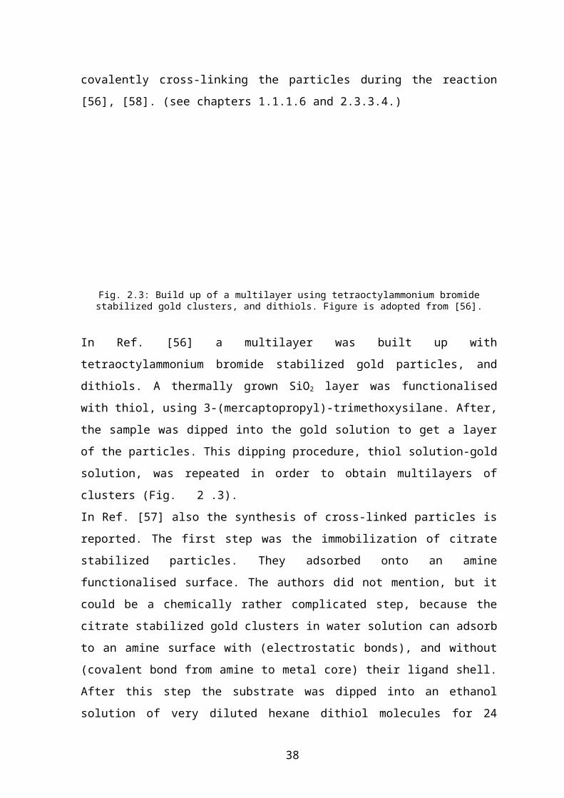
future use and explains why the electrical properties of the Au55 cluster must be investi-
gated.
2.4.4 Importance and strategy of the ligand-exchange
As already mentioned, the organic ligands PPh3 makes the Au55 cluster soluble in organic
solvents and insoluble in water. In order to solubilize it in water, ligand exchange reaction
is necessary using a phase transfer reaction (the method was already described in chapter
2.3.2) [120]. A dichloromethane solution of Au55(PPh3)12Cl6 clusters is mixed vigorously
with a water solution of PPh2(C6H4SO3H). During the phase transfer reaction, the other
molecules, soluble in water, exchange the PPh3. This can be visualized by a brown col-
oration of the colorless aqueous phase. The experiments showed that the
Au55[PPh2(C6H4SO3¯)]12Cl6 cluster is more stable in solution what is caused by the relative
big charge hold by the particle.
The same strategy was followed also in the case of T8-OSS [121] and disodium-mercap-
toundecahydro-closo-dodecaborate (BSH) (Fig. 2.13). The affinity of these two ligands to
Au55 is higher than that of PPh3 molecule because of the thiol groups, so the Au55 is easily
transferred to the aqueous phase. This transfer reaction helped also to purify the sample
and to quantify the reaction, as it is written in chapter 2.3.2.2.
a) b)
Fig. 2.13: The T8-OSS (a) and BSH (b) ligands. Figure is adapted from [121] and [122].
The experience was that the exchange of the ligand shell changes the properties of the clus-
ters dramatically. The Au55(PPh3)12Cl6 is relatively stable in solid phase under atmospheric
conditions, but its lifetime in solution is not more than a few hours [120]. This is because
of the equilibrium reaction, which takes place in the solution:
MLy + k S → MLy-kSk + k L 2.16
40
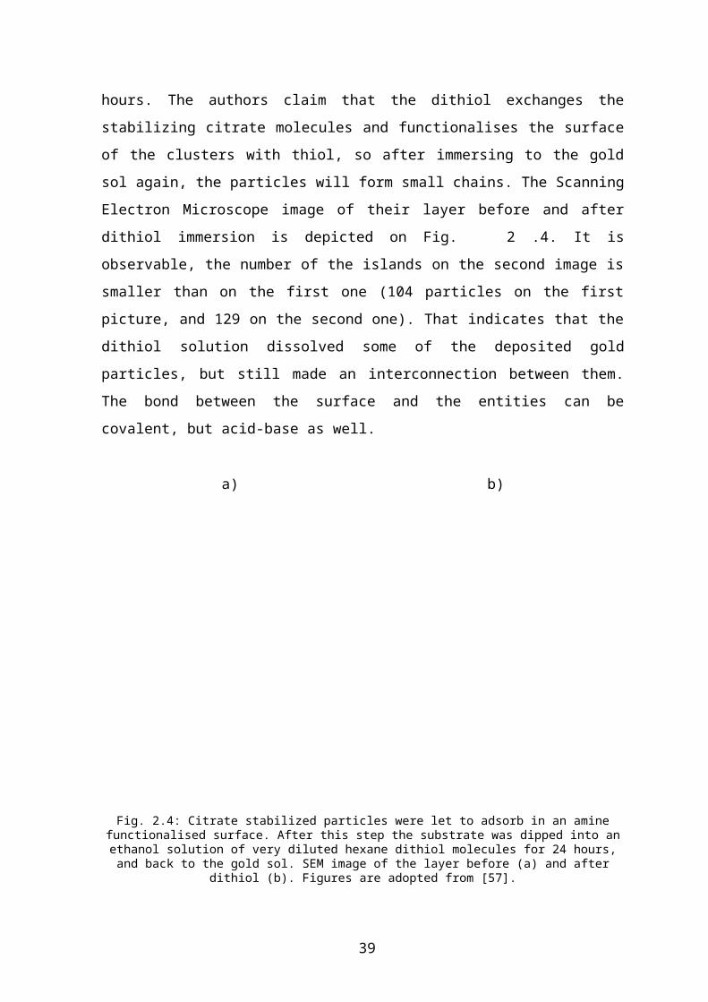
where M in the metal core, L is the ligand and S stands for solvent molecules. If too many
ligands become free, the weakly stabilized metal cores stick together, forming a bigger par-
ticle. `The aggregation can be observed by the change of the color of the solution. Letting
the Au55(PPh3)12Cl6 cluster in solution for two or three hours the originally dark brown so-
lution becomes purple, and in additional one hour, blue. After a night, a black precipitate
can be observed, showing, that during the aggregation metallic gold is formed. The
Au55(T8-OSS)12Cl6 cluster is stable in solution for almost infinite time. That is because the
big ligand shell, which doesn’t let the clusters too close to each other, but also, because of
the reaction constant of the above explained reaction is very small, so there are simply no
attackable metal core.
Of course ligands can also be exchanged by simply mixing the Au55(PPh3)12Cl6 clusters
with a thiol ligand[114][123]. In this case the stronger Au-S bond can exchange the weaker
Au-P bond. The problem of this synthesis usually is to get rid of the free PPh 3. As it is ex-
plained in chapter 2.3.2.3, the ligands can also be exchanged on the surface. For this, a
thiol functionalised surface is used, and a solution of the Au55(PPh3)12Cl6 clusters. In this
case the gold core is anchored to the surface with formation of an Au-S bond and some of
the PPh3 from the ligand shell become free.
2.4.5 Preparation and properties of zero-, one -, two–, quasi-two-, and three-dimen-
sional arrays of Au55 cluster.
2.4.5.1 Zero-dimensional arrangements
Zero-dimensional arrangements of Au55 clusters can be prepared by dropping a very dilute
solution onto a substrate. Using the same deposit method on a carbon coated copper grid,
TEM measurements have shown, that the size of the metal core is 1.4 nm [1].
STM investigations of Au55[PPh2(C6H4SO3¯)]12Cl6 layers were also realized. Such layers
were obtained by a chemical method: a glass surface covered with cysteamine-hydrochlo-
ride was dipped into an aqueous solution of the water-soluble Au55[PPh2(C6H4SO3¯)]12Cl6
cluster. The as-prepared monolayer was investigated by STM, perpendicular to the surface
41
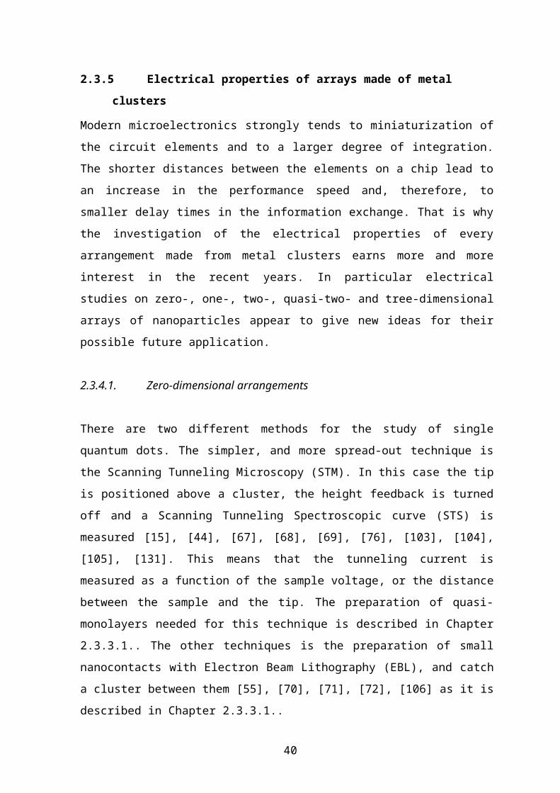
[128][133]. These measurements gave an important result: with the STM method, the clus-
ters are 2.1 nm high. That means, that the ligand shell also influences the mechanism of the
electron transfer through a particle.
2.4.5.2 One-dimensional arrangements
There are four strategies for the preparation of one-dimensional arrangements of the Au55-
cluster:
- The first and oldest method is to immobilize the clusters in alumina nanotubes
[134]. The clusters stabilized by T8-OSS (diameter size: 4.2 nm), were introduced
into the pores (diameter: 7 nm) by means of electrophoresis (Fig. 2.14). Inside the
nanotubes, the clusters form a spiral-like structure, as it is illustrated in Fig. 2.14.
The clusters, finding each other as well as to the pore wall by van der Waals inter-
actions, since the T8-OSS ligand has no functional group in the direction of the
pore walls.
Fig. 2.14: Alumina nanotubes filled with Au55 (T8-OSS) 12Cl6. The left picture is a TEM image of a nanotube inside, the right picture is a schematic drawing of the filled pore. Figure is adapted from [134].
- The second strategy couriers the use of DNA. t can also be used as a template to in-
duce clusters arrangement via chemical interaction: a quartz platelet is dipped into a
solution containing the DNA and clusters. The clusters arrange themselves along
the DNA on the surface via specific bonds to form wires.
42
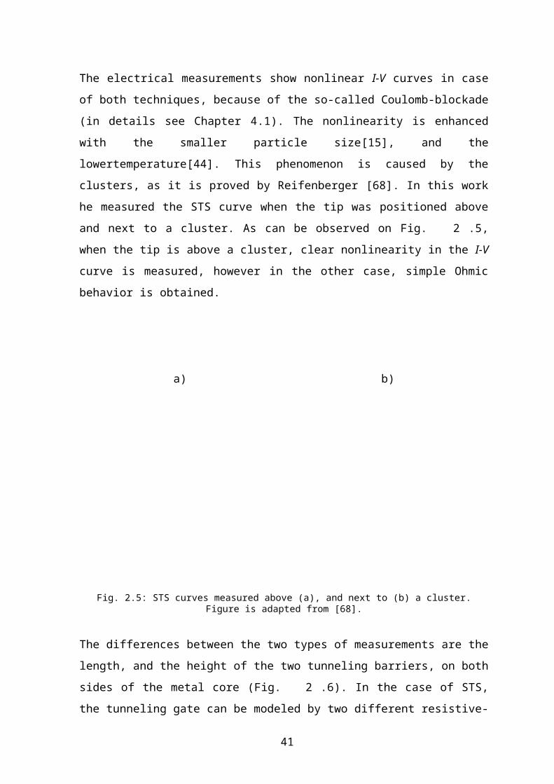
- Third strategy: Nanowires were generated by trapping the clusters between two
nanocontacts with application of a voltage between the electrodes. A platelet with
the contact structures was dipped into a Au55(PPh3)12Cl6 dichloromethane solution
and 1V was applied between the electrodes. As long as the distance between the
electrodes is 20 to 30 nm, a short row of clusters is trapped, arranging themselves
along the lines of the electric force. As can be observed in Fig. 2.15, more cluster
liner are formed during the preparation, drawing the lines of the electric force. The
shortest line of these is, of course, the linear between the two contacts [155] (Fig.
2.15). This line in the middle of the picture seems to form a closed line which al-
lows the flow of the electric charge through it. The electrical measurements through
this line can be observed in chapter 2.4.6 and on Fig. 2.21.
Fig. 2.15: Clusters arranged along the line of the electric force between two W tips. Figure is adapted from [155]
- The fourth trial is the preparation of quasi-one-dimensional structures using LB
technique and the oscillation of the water meniscus. During the transfer process of
the monolayer to a substrate, a periodic oscillation of the water meniscus induced a
breake of the monolayer with the same periodicity [135] (Fig. 2.16). This move-
ment allows the formation of stripes (thickness: 6 nm) parallel to the direction of
the meniscus and perpendicular to the movement of the sample.
43
Fig. 2.16: Stripes prepared by LB technique. The sample is pulled out from the solution with a relative high speed, so that the meniscus breaks periodically. The stripes are parallel to the direction of the meniscus, and
perpendicular to the movement of the sample. Figure is adapted from [135].
2.4.5.3 Two-dimensional arrangements
The preparation of two-dimensional arrangements of Au55 clusters was also a big chal-
lenge, and was solved during the last three years. Building large closed areas clusters is
necessary to characterize them electrically.
As mentioned in Chapter 2.3.3.3, two main methods are available for the preparation of
cluster monolayers. Chemical methods are starting with the modification of a surface, fol-
lowed by specific adsorption of clusters. Physical methods are more or less based on modi-
fied LB techniques.
In recent years, the most important work concerning the chemical methods were realized
by S. Peschel and M. Bäumle [125][126]. They worked mostly with layers based on ionic
interactions, using polyethylenimine (PEI) as cationic polymer, and the water-soluble gold
cluster as anionic cluster. Two kinds of acid-base ionic interactions are present: between
the negative glass surface, and the positive polymer (the imino groups in the polyethylen-
imine receive a proton from the hydroxyl group of the glass surface) and between the posi-
tive polymer, and the negative clusters (-SO3H + -NH2 →-SO3¯ + -NH3
+) [136][137]. This
method was convenient for mica, silicon and glass substrates. For gold substrates another
method was used: the surface was covered by small linker molecules like aminothiols, e.g.
44

cysteamine [125] (see chapter 2.3.2.3). With this technique smaller or bigger islands of
closed monolayers were obtained, however, only small range ordering was observed..
Covalent bonds between surface and cluster were never used to obtain monolayers on dif-
ferent substrates. Specific interactions based on covalent bonds were used to immobilize
clusters inside pores [138], but this technique was not convenient for preparing closed
monolayers onto flat surfaces.
Some trials to order clusters onto different substrates using modified LB technique(s) were
also realized [139] (Fig. 2.17). Some drops of a Au55(PPh3)12Cl6 dichloromethane solution
were deposited onto a very diluted aqueous solution of different amphiphile compounds,
like per-6-deoxy-6-thio--cyclodextrin or poly-vinyl-pyrrolidone. After evaporation of the
solvent, a carbon coated copper grid was dipped carefully under the surface of the liquid
and pulled out slowly to transfer the layer. The samples were investigated by TEM.
Fig. 2.17: Sketch of the cluster-amphiphile interaction on the interface between the dichloromethane and the aqueous solution. Figure is adapted from[139].
With this technique, relative big islands of ordered monolayers (up to 1 m in diameter)
were obtained. The clusters crystallized in two different forms: hexagonal arrays and
square lattices.
45
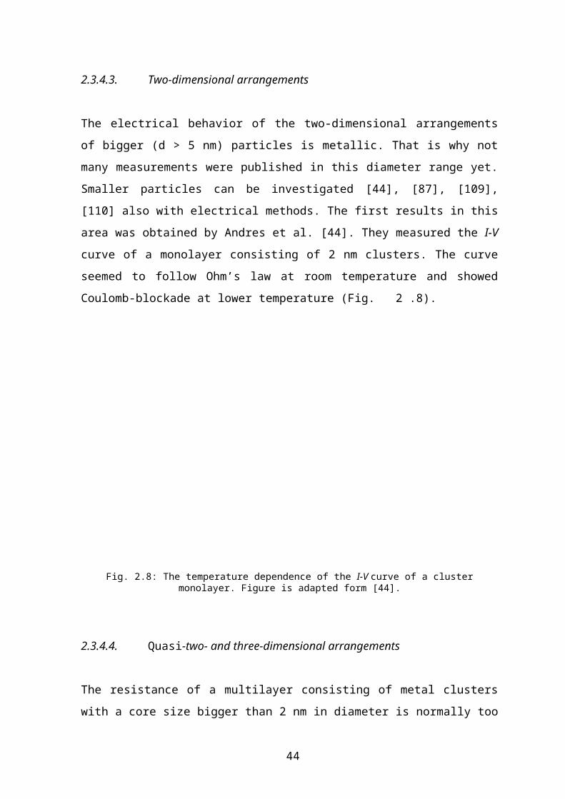
2.4.5.4 Quasi-two-dimensional arrangements
Thin films of the Au55 clusters are prepared mainly by two methods: spin-coating, and
layer-by-layer self-assembly.
During the spin-coating technique, the formation of thin film owning relative homoge-
neous thickness is possible [140][141]. A quartz plate is spinning with a certain speed and
some droplets of a cluster solution is dropped onto its surface. The thickness of the film is
controlled by the speed of the platelet and the concentration of the drops (Fig. 5.24).
The layer-by-layer self-assembly methods are working on the same basis as those using
bigger particles, discussed in chapter 2.3.3.4. In this case mainly ionic self-assembled lay-
ers were used [125][126]. A monolayer of the Au55 clusters was prepared, as it is intro-
duced in chapter 2.4.5.3 and the clusters dipped back to the PEI solution, which built up a
second polymer layer on the surface. The sample then was dipped into the water-soluble
cluster solution, arranging the second cluster layer, and so on.
2.4.5.5 Three-dimensional arrangements
Microcrystals of hexagonally ordered Au55(PPh3)12Cl6 cluster are easy to prepare, from
CH2Cl2 solution by simple evaporation of the solvent.
Ordered cluster arrangements with different cluster spacings can be built using clusters
with different ligand shells (see chapter 2.3.2). With PPh3, for instance, the distance be-
tween the centers of two neighbored clusters is 2.1 nm, while in the case of T8-OSS ligand
is 4.1 nm. Spacers also can be used to get different lengths between the gold particles
[123], [114], [41]. In this case, acid-base interaction between the SO3H group of the
Au55[PPh2(C6H4SO4H)]12Cl6 clusters and the NH2 group of the ligands were used.
The tuning of the distance between the particles without changing their ligand shell is an
important experiment [123], [114], [41] (Fig. 2.18).
46

Fig. 2.18: Tuning the distance of the clusters with spacers. Figure is adapted from [41].
The easiest method to get such structures is to mix the aqueous solution of the water-solu-
ble cluster and an --diamine and let it crystallize. In this case ionic bonds are formed be-
tween the -SO3¯ and the –NH3
+ groups, and the spacers are wedged in the cluster space.
These reactions are not ligand exchange reactions, rather an inter-shell reaction with an-
other spacer. Three different molecules were used for testing this reaction [125]: 4,4’-di-
amino-1,2-diphenylethan (DDE), bis{5-[(4-aminophenyl)ethinyl]-3-methyl-thien-2-
yl}acetylen (BATA) and 1,4-bis{3-propionic acid[1-(8-N-pyridiniumbromide]
octylester]}benzene (POB) (Fig. 2.19). With TEM and electrical measurements it was
proved, that the inter-cluster distances were different according to the ligand used. (In de-
tails see chapter 5.2.3.1).
a) DDE b) BATA
c) POB
Fig. 2.19: The three molecules, used for tuning the distance between the clusters. Figure is adapted from [123].
47
For quasi-two-dimensional arrangements spin coating technique was used (see chapter
2.4.5.4 and Fig. 5.24). For the preparation of a monolayer a modified LB technique was
applied (with a slight modification of the method described in Ref. [139].)
2.4.6 Electrical properties of arrays made of Au55 clusters
The size, the composition, and the shape uniformity of the Au55 cluster together with its
very small capacitance makes it the optimal object for the investigations of easily pro-
ducible room-temperature SET. This fact was proved by electrical measurements realized
on both zero- [124][128] and one-dimensional [155] arrangements (Fig. 2.21).
If an STM tip is positioned above a Au55 cluster, the STS curve shows strong Coulomb-
blockade. A Coulomb-staircase at low temperatures is also observable (Fig. 2.20).
It turned out that, using EBL fabricated nanocontact systems with a source-drain distance
of 20-30 nm from each other, and a gate electrode a little farther (Fig. 2.15); nanowires of
clusters can be trapped between the source and the drain (see chapter 2.3.4.1 and Fig.
2.15). Measuring the I-V characteristics of these systems, Coulomb behavior was obtained.
The change of the gate potential causes a change in the I-V curve between the source and
the drain, which indicates that a SET was fabricated [155] (Fig. 2.21).
a) b)
Fig. 2.20: The STM tip is positioned above a single Au55 cluster and I-V characteristics is measured. (a) The STS curve shows Coulomb-blockade behavior at room temperature. (b) Coulomb-staircase behavior at 90 K.
Figure is adapted from [124].
48
Fig. 2.21: The I-V characteristics of the first single electron transistor fabricated from the Au55 cluster. The changing of the gate potential leads to the change of the I-V curve between the source and the drain, which
indicates that a SET was prepared. Figure is adapted from [155].
Many difficulties concerning the electrical characterization of the monolayers are exist.
First of all, the resistance of the Au55(PPh3)12Cl6 cluster systems are too high to be mea-
sured with simple methods. These cluster systems behave as insulators also in 3D. The re-
sistance of a system consisting of two electrodes and the sample depends also on the size
of the electrodes (see chapter 4.3.3). In the case of two-dimensional measurements the
“area” of the electrodes are very small.
On the other hand, these monolayers consist of closed-packed cluster islands in most cases.
To be sure to really contact them, conducting paths with very small distance have to be
used. This also useful, because decreasing the electrodes distance involves a decreasing of
the system resistance.
Furthermore, the monolayers prepared until now were mostly layers based on ionic bonds
(see chapter 2.4.5.3). In this type of arrangements conductance of the layer caused by the
ionic movements in the residue water and the polymeric medium can be one or two magni-
tude higher, than the conductance of the clusters.
Thin films of the clusters are easier to measure than the monolayers. The areas of the elec-
trodes used are bigger, since the thickness of the layer is bigger, and with spin-coating
technique, for instance, homogeneous and quite thin films can be prepared (see chapter
2.4.5.4). Using Au55(PPh3)12Cl6 clusters no ionic interactions are used, so no movable ions
in the layer can interact and this point represents the biggest advantage of this synthesis
49

technique. Because of the bigger electrode area and because the film is much more homo-
geneous than in the case of a monolayer, bigger electrode-distances can be used.
The most obvious idea to study the conductivity of a sample having relative big resistance
is the three dimensional characterization. In this case depending on the used geometry, the
electrode surfaces can be relative big compared to their distance, so the conductivity can be
increased into the easily measurable range. The pioneering work in this field was made by
L. J. de Jongh and coworkers [142]. They measured the temperature dependence of the
conductivity of three-dimensional Au55 systems and observed, that the kinetics of the elec-
tron transport in this systems doesn’t follow the Arrhenius law, because the logarithm of
the conductivity is not linear as a function of the reciprocal temperature, just as a function
of the square root of the temperature. (see chapter 4.5.3) This observation makes the Au55
cluster systems similar to the so-called cermets, which are metal-insulator composite mate-
rials.
The authors discuss numerous theories to describe this behavior, and find that the variable
range hopping models namely the thermally activated stochastic multiple-site hopping
process fit the measured data best. At high temperatures the nearest neighbor hops domi-
nate (see chapter 4.5.3).
A simpler explanation of this behavior was worked out by Mott in 1969 [149][150][151].
This is the Mott’s conduction theory for the Variable Range Hopping (see chapter 4.5.3).
50
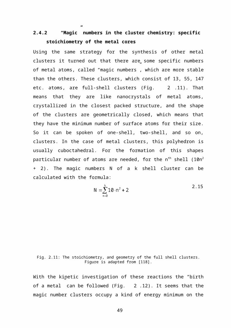
3 Aim of this work
The investigations focused on the following points:
1. Experimental conditions for the electrical measurements
2. Dependence of the charge transfer mechanism and the activa-
tion energy on the ligands
3. Electronic properties of Au55 monolayers
The studies will be carried out separately for two-, quasi-two-, and three-dimensional ar-
rays of Au55 clusters. From the viewpoint of the experimentalist, the following problems
have to be solved for the two-dimensional-samples:
1. A monolayer consisting of large, dense-packed Au55 islands should be prepared. For
successful electrical measurements, this layer should not contain movable ions like
Na+ or traces of conducting solutions (aqueous solutions, impurities).
2. The monolayer has to be transferred onto the substrate applied with the electrode sys-
tem. This electrode system should contain electrodes in a suitable geometry and size
range.
3. Suitable parameters should be elaborated for the cross-linking reactions, without
changing the structure of the monolayer.
For the quasi-two-dimensional samples:
1. Multilayers of Au55 clusters should be prepared, without movable ions or traces of
ion-conducting solution.
2. A suitable method should be found for the chemical attachment of the multilayer
onto the substrate surface.
For the three-dimensional samples:
1. Conjugated ,-dithiols should be synthesized to function as bridging ligands.
2. Cross-linking of the clusters with ligand-exchange reactions.
The conductance of samples with quasi-two- and three-dimensional cluster arrangements
can be characterized with the methods elaborated by U. Simon. However, novel measure-
ment techniques need to be developed for monolayers with a two-dimensional cluster ar-
chitecture.
51
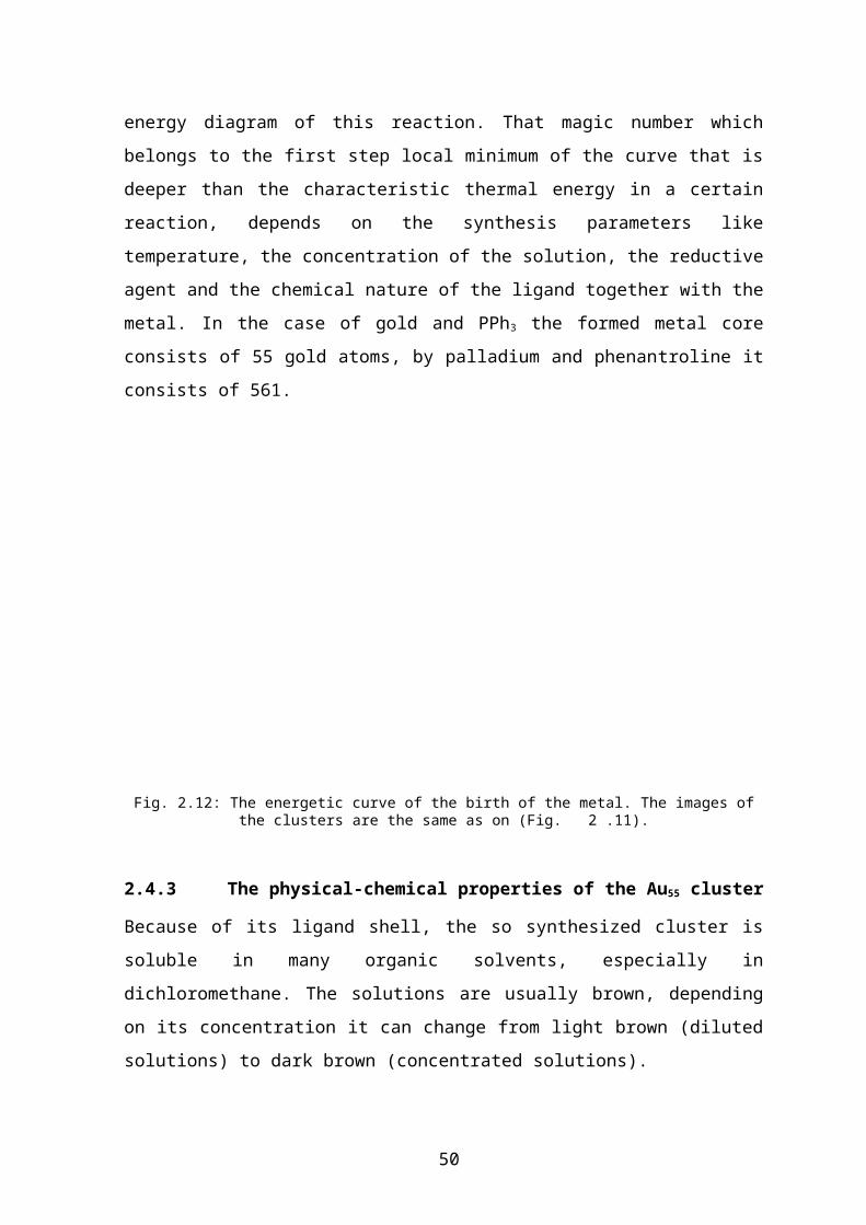
4 Discussion of the charge-transfer mechanisms in nanoparticle systems
To understand the problems and the results, which will be discussed in the following chap-
ters (chapter 5 and 6), some principle studies on the electron transfer mechanisms of differ-
ent cluster arrangements is necessary. It will be shown, how the charge transfer mechanism
of a complicated three-dimensional sample can be built up from the flow of current trough
single nanoparticles. In the following this background will be overviewed and discussed.
4.1 Conduction mechanism of zero-dimensional systems (tunneling
through a quantum dot)
The literature overview of the tunneling through a quantum dot is discussed in chapters
2.3.4.1 and 2.4.6. The main and common points in these measurements are that the capaci-
tance of the central island in a SET has to be decreased, to increase the temperature thresh-
old of the single electron tunneling effects. The basics of the single electronics is discussed
in chapter 2.2. There are mainly four signs that indicate a SET: the Coulomb-blockade, the
Coulomb-staircase, and the oscillating dependence of the source-drain I-V characteristics
on the gate potential. This is supplemented with the Size Induced Metal-Insulator Transi-
tion effects (SIMIT effects) in the case of small metal particles, which is not strictly a sign
of the presence of a SET, but influences the shape of the I-V curve.
A single electron transistor consists of a small metal island (metal nanoparticle) and three
electrodes: the source and the drain are close to the central island, the gate is a little farther,
coupled capacitively to the central island (see Fig. 2.2). Using the single electronics lan-
guage, the set consists of a double junction system, with an electrode (gate) capacitively
coupled to the central island. If the electron pass through the first junction, it charges the
central island, which causes the voltage drop to change with a value of e/C (where e is the
charge of the electron, and C is the capacitance of the junction). This is the cause of the
Coulomb-blockade effect: the tunneling is suppressed at voltages V<e/2C. If the
Coulomb-blockade do not exist, than at voltages V<e/2C the tunneling would increase the
electrostatic energy of the capacitor C(V e/C)2/2 > CV2/2. The Coulomb-blockade is de-
52
termined only by the first junction: if the two junctions are different, asymmetry in the I-V
characteristics can be observed, which is caused by the two different Coulomb-blockades
from the two different directions (normally this is the case by STS measurements. See E.g.
Fig. 6.2). Concrete examples for the Coulomb-blockade behavior can be observed in Fig.
2.5 and Fig. 2.20.
If the tunnel junction of the SET is considerably different, then the I-V curve shows sub-
stantial periodic oscillations with a period of V = e/C1 (for R1>> R2, where R1 and R2 are
the tunneling resistances of the two junctions). This is the Coulomb staircase. Each period
of the staircase corresponds to an additional electron on the central island [107]. This effect
is typical for the STS measurements, because the tunnel junction between the conducting
particle and the substrate is usually much smaller, then those between the tip and the parti-
cle.
The third effect is that the value of the Coulomb-blockade depends on the background
charge of the central island. This can be controlled by a third electrode (gate), which is ca-
pacitively coupled to the central island, in order to control its charge. Using the theoretical
equations of the SET, it can be concluded that the Coulomb-blockade completely disap-
pears, if the background charge is equal to (k+1/2)e (k is an integer) because the states with
effective charges of e/2 and -e/2 have equal energy.
The transition from single atoms or molecules to the metallic state contains many dramatic
changes in the electron energy levels. These effects are the so-called quantum size effects
(QSE) (Fig. 4.1) [124][129]. In this transition (Size Induced Metal to Insulator Transition,
SIMIT), there is no well-defined threshold, the change is continuous, and the results de-
pend strongly on the measurement method.
The I-V characteristics of a SET transistor with a level discreteness contains step-like fea-
tures which appear, when the discrete level in the island crosses the Fermi-level (HOMO
electron level in the metals) of the external electrode. The SIMIT can interfere with the
Coulomb-staircase forming a quite complicated electronic behavior. Sometimes it is diffi-
cult to distinct between the two effects (Fig. 2.20), except when the Coulomb staircase has
equal periods, while the SIMIT effects are random, depending on the energy level of the
nanoparticle.
53
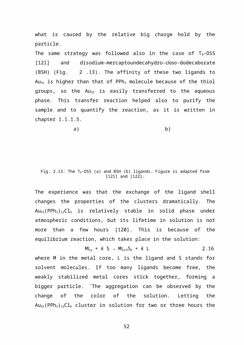
Fig. 4.1: Electronic situation in (a) bulk metal particle with quasi-delocalized d and s electrons forming a band structure. In (b) the electrons begin to form discrete energy levels which are completed in the molecular
state (c) with fully localized bonding electrons. Figure is adapted from [124].
Reifenberger and coworkers [152] have investigated the influence of the chemical nature
of the ligands on the STS curve. They measured the STS curve of conjugated molecules
with different functional groups at the ends. They have found that STS spectra can be re-
ally different when a molecule is linked to a substrate or to a STM tip with different chemi-
cal interactions. This effect can be explained by the conductance of the molecules through
the HOMO or the LUMO orbitals. The place of the Fermi level is changed according to the
LUMO of the investigated molecule, depending on the chemical nature of the function
group. In the case of an STS measurement the voltage drops on the molecule is 1─4 V,
which can cause the distribution of the electrons between the HOMO and the LUMO: the
electrons can be really excited from the Fermi level of the substrate or the STM tip to the
energy of the LUMO of the spacer molecule. The same effect has also to be taken into con-
sideration in the case of nanoparticles: the nature of the chemical interaction between the
substrate and the particle can influence its conductivity. It will be discussed later that this is
not the case at measurements with higher dimensionality (see chapter 5.2.3.4).
4.2 Conduction in one-dimensional arrangements
One-dimensional arrangements of metal nanoparticle systems cannot be considered as a
double-junction system any more, but like a multi-junction system. In other words, there
are two electrodes and many tunnel junctions between them. That arises two kinds of prob-
lems in the case of ligand-stabilized clusters. The first is that the separation of conducting
particles is larger, so the junction is thicker, because the distances between the metal cores
54
are equal to the length of two ligand shells. The thickness of the junction increases the tun-
neling resistance, which depends exponentially on the distance between the particles. In the
case of smaller clusters this effect generates experimental difficulties.
The second problem is the question of the possible disorder in this system. Small disorder
in the arrangement causes big differences in the measured data [108]. The authors have
discussed the impurities effect (smaller particles in the array) and the packing defects (the
inter particle distances are very different at certain places). The main conclusion was that
the impurity increases the potential at that point, which may lead to, at least, localization:
the single electron in the array may be trapped. The packing defects influence the capaci-
tance at that point of the array.
The conduction in disordered nanoparticle systems with a higher dimensionality occurs
trough conducting paths. These are one-dimensional rows of clusters inside an array with
higher dimensionality. These rows were chosen by the flowing current, because the resis-
tance of these ways is smaller than any other in the region. (For better understanding see
Fig. 4.3).
The two main experimental results, which give peaces of information about the electrical
behavior of one-dimensional arrangements, are discussed in chapters 2.3.4.2 and 2.4.6.
4.3 Conduction in two-dimensional arrangements
4.3.1 The effect of the impurities and displacements
Adding one more dimension to the system the conduction becomes even more compli-
cated.
The problem of the impurity does not pose problems any more, because the conduction
paths (the way of the electrons through the arrangement) choose directions among the clus-
ters, which are in the absence of this small disorder effects (Fig. 4.2a). The same can be
predicted for small numbers of displacements in an ordered lattice (Fig. 4.2b), system
“heals” itself.
a) b)
55
Fig. 4.2: Conducting paths in the case of the presence of an impurity (a) or displacements (b).
4.3.2 The conducting paths
In the case of island-like structures of a monolayers (which is quite common in nanoparti-
cle systems) the conductance mechanism is more complicated.
a) b)
Fig. 4.3: Island-like structure of a nanoparticle system. In the inter-particle region the clusters arranged statis-tically (a) or build up conducting paths (b).
In this case, more or less ordered islands alternate with regions of smaller conducting parti-
cles density (Fig. 4.3). The charge transfer mechanism of these arrangements can be ex-
plained with a theory, which is similar to the Brick layer model developed for three-dimen-
sional samples, and discussed in chapter 4.5.2 in details.
Two possibilities can be observed (see Fig. 5.10 and Fig. 5.11). The first corresponds to a
statistical arrangement of the particles in the inter-island region (Fig. 4.3a, Fig. 5.10). In
this case there is no conducting path between the islands: it is the insulator case. The acti-
56
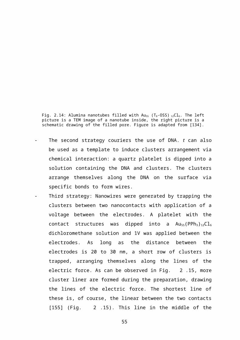
vation energy of the sample is very high: the clusters have to move to build conducting
paths. In Fig. 4.3b another arrangement can be observed (see also Fig. 5.11): the particles
build conducting paths in the inter-particle regions. This model is also discussed in details
in chapter 4.5.2. So, these regions have larger resistances than the intra-particle regions,
but this can be explained by the smaller number of the conducting paths.
A nice example concerning to the building of conducting paths can be observed in the case
of comb structures with relative high applied voltage (Fig. 4.4). In this picture every sec-
ond white line (tungsten wire) are electrically connected with each other: the 1st, 3rd, 5th and
so on upwards, as well as the 2nd, 4th, 6th and so on downwards (see Fig. 8.5). That means,
that if voltage is applied to the electrodes, this voltage falls between the neighboring wol-
fram lines, represented by the white lines in the figure. If the applied voltage is high
enough, the clusters can move to build conducting paths, as it can be observed in the cir-
cled areas in Fig. 4.4.
Fig. 4.4: Conducting paths built as an effect of the high applied voltage.
57
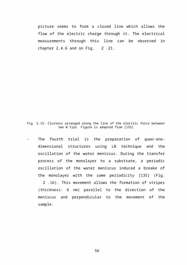
4.3.3 The effect of the electrode-geometry
In the case of a homogeneous sample with “infinite”* long electrodes on the surface, a clear
Coulomb-behavior should be observed. That means that in the metallic case the I-V curve
is simply linear, or in the presence of SET effects it is a Coulomb-blockade with two linear
branches on the sides (Fig. 4.5). Measuring on real samples, even in the case of practically
infinite long electrodes (comb structures) nonlinearity effect can be observed. That means
that the I-V curve is not linear in any voltage regions. This can be explained with the dif-
ferent lengths of the conducting paths: at small voltages (small activation energies) only
the shortest paths are available, at higher voltages can others also become active. The indi-
vidual currents of the different paths are superimposed to give the macroscopically mea-
surable current I.
a) b)
Fig. 4.5: Theoretical (a), and measured (b) I-V curves in the case of homogeneous layers between two not in-finite electrodes.
In the case of non-infinite electrodes even the electric measurement of a homogeneous
layer results in a nonlinear I-V curve (Fig. 4.5).
* “Infinite” long in this sense means that the length of the electrodes on the surface perpendicular to the direc-
tion of the flowing current is very long comparing to their distance.
58
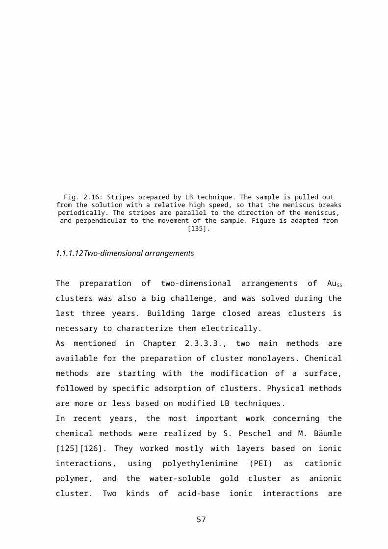
Fig. 4.6: Conducting paths of a homogeneous sample in the case of non infinite electrodes.
This effect is caused by the different conducting paths, which are more and more available
with the increasing of the voltage (Fig. 4.6). In Fig. 2.15 this effect can be observed. This
sample was prepared by applying a voltage between two electrodes in a Au55(PPh3)12Cl6 so-
lution. The clusters arranged along the electric force lines as it is discussed in chapter
2.4.6. The conductance of this sample is nonlinear, because with increasing of the voltage
more and more paths become active. The currents flowing trough the individual paths are
summed up: the conductance of every individual path is linear, but they become conduc-
tive on different voltages, so their sum is not linear any more.
4.4 Conduction in quasi-two-dimensional arrangements
In thin films built by superposition of many nanoparticles monolayers, the number of the
conducting paths increases and the possibility of having statistically arranged areas de-
creases, so the activation energy and the resistance of the layers are dramatically de-
creased.
The rules that determine the conductance in a thin film are exactly the same as in two and
in three dimensions. It is a transition state, which results in a transition behavior. Numer-
ous monolayers piled up may behave as well as a monolayer with many conducting paths,
59
and as a thick film like a three dimensional arrangement. One sign of this effect might be
the dependence of the activation energy on the layer thickness.
4.5 Conduction in three-dimension (conduction in non-homogeneous
solids)
4.5.1 The absence of the Coulomb-blockade
With the increasing of the thickness of a quasi-two-dimensional layer into three-dimen-
sional the parameters of the layer become constant. These values are average values of the
microscopic characteristics. Models are developed to understand this situation, which will
be discussed in the following.
The first and most apparent behavior of the three-dimensional systems is the absence of the
Coulomb-blockade. This effect is clear and undisturbed in zero- and one-dimensional sam-
ples. In the two-dimensional arrangement, the Coulomb-blockade can always be observed
if Au55 is used. In quasi-two-dimension, it depends strongly on the temperature, the ligand
shell and the thickness of the layer, and in three-dimension there is no Coulomb-blockade
behavior. There are two effects at the origin of this phenomenon. First, on a three-dimen-
sional sample, numerous conducting paths, with numerous microscopic capacitance are
present. The longer is a conducting path, the smaller is the capacitance of it, which means,
that a longer conducting path has a bigger Coulomb-blockade value. In the case of a
macroscopic sample these values follow continuously each other, which result in a soft
border of the zero conductance.
On the other hand, an increasing of the thickness of a layer results ultimately in an in-
creased number of conducting paths. That means, that the capacitance of a three-dimen-
sional arrangement decreases so, that the Coulomb-blockade effect disappears.
An evolution of the Coulomb-blockade can be observed on the following pictures: In the
case of Au55(PPh3)12Cl6 cluster the conductance curve of the monolayer can be observed in
Fig. 5.19, those of an asymmetrical thin film on Fig. 6.3 and the thicker film with bigger
electrode on Fig. 5.26.
60
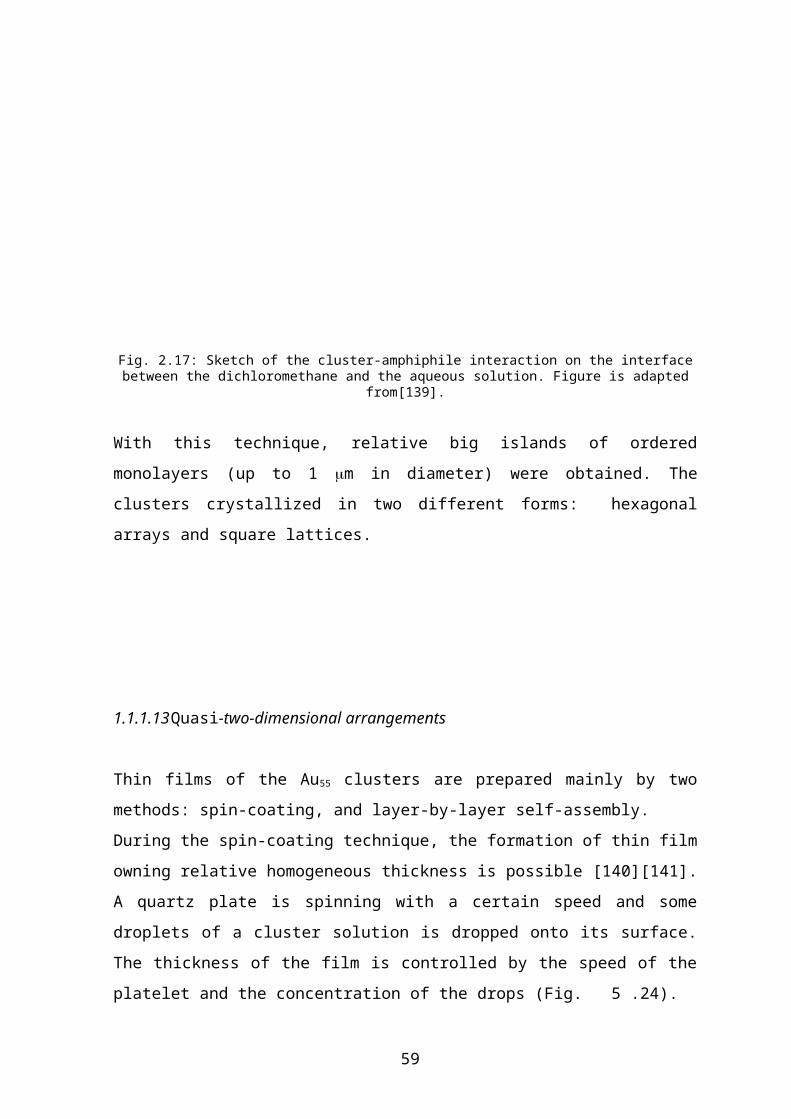
The same transition happens in a smaller thickness range in the case of the cross-linked
systems: the conductance curve of the monolayer is on Fig. 5.21, and those of the thin film
is on Fig. 5.31.
4.5.2 Brick layer model
There are many models that can be used to explain the conducting properties of non-homo-
geneous solids. The Brick layer model [153][130] (Fig. 4.7) proved to be the most useful
for our Au55 systems.
Originally the brick layer model was developed to explain the conductance of cermets.
These are metal-insulator composite materials, with metal islands inside, separated metal-
oxide insulators. A typical example is the evaporation of Al in the presence of different
amount of oxygen. If the percentage of O2 is large, mainly Al2O3 forms. Without the pres-
ence of oxygen Al metal grows. Between these two limits there is a threshold ratio. If the
sample contains more Al than this value, more and more metal islands will be formed in-
side the material, which gives the possibility of conductance. It will be pointed out in the
following, that this material has numerous similarities in the conductance mechanism with
the cluster systems. This is not very surprising, since the clusters are also metal-insulator
composite materials, with the metal cores as metal islands and the ligand shell as insulator
medium.
The “bricks” constitute the main part of the material. The grain boundaries are the small ar-
eas with exceptional behavior. If the conductance of the grains is smaller than that of the
grain boundaries, the electrons move trough the grain boundaries without disturbing the
grain interiors phases. If, however, the conductance of the grains is larger, the grain bound-
aries act as a gap in the way of electrons. In this case the electrons have to hop through the
higher resistance regions. The conducting path can be built up, or can simply exist inside
the grain boundaries. These are paths where the resistance is smaller than at other places in
the grain boundaries.
In the terminology of cluster systems, bricks or grain interiors are the densest packed re-
gions, where the electrons can tunnel through the hopping bands. This material is an isola-
tor or a semiconductor, depending on the ligands. The impedance spectrum of this process
61
is a simple Debye semicircle [130], equivalent to a simple Resistance-Capacitance (RC)
circle, indicating the regularity of the electron-conducting arrangement. The grain interior
phases are cluster displacements in the lattice, or impurities, which disturbs the regular
densest packed order in the material. The electrons have to hop through these regions
following a temperature-activated process.
Fig. 4.7: Description of the brick layer model: (a) the bricks are the densest packed cluster groups inside the material, the grain boundaries are the disturbed regions. (b) Inside the bricks the conduction mechanism is
the tunneling in the hopping bands, opposite to the hopping inside the grain boundaries. The figure is adapted from [130].
The impedance spectrum of this process is the not so regular Cole-Cole curve, which is
equivalent to a resistance coupled parallel with a so called constant phase element, (CPE)
[153]. This curve implicates the irregularity of the system (Fig. 4.8).
62
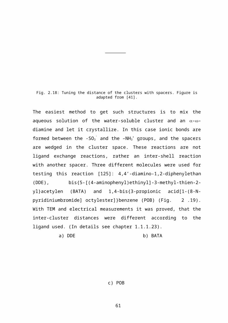
The in chapter 4.3 explained nonlinearity of the I-V curve will now be discussed in terms
of the brick layer model. Depending on the activation energy and the thickness of the grain
interiors, an increase in voltage increases the number of the available easy paths (one-di-
mensional conducting paths), resulting in a nonlinear I-V behavior.
a) b)
Fig. 4.8: Impedance of the system, which can be characterized by the Brick layer model. The sign I on the (a) figure is the Debye semicircle, and the Sign II shows the electric circle of the Cole-Cole process. On figure
(b) impedances of the two process can be observed.
4.5.3 Variable range hopping models
For simple reactions, the temperature-dependence of the reaction rate for a follows the em-
pirical Arrhenius law. This proclaims, that the logarithm of the reaction rate depend linear
on the reciprocal of the temperature. The conductance of the semiconductors, being a tem-
perature-activated reaction, also follows this rule. The conductance of metals is in contrast
not a temperature-activated reaction, since there is no energy gap around the Fermi level.
The temperature dependence of the resistance depends therefore on an other effect, namely
on the electron phonon scattering.
The conductivity of cluster systems should at first approximation be similar to that of semi-
conductors. This is true at high temperatures. As mentioned in chapter 2.4.6, the pioneering
work of de Jongh showed, that in analogy with the cermets the temperature-dependence of
the conductivity of Au55 cluster systems also follow lnC (1/T1/2) proportionality [142],
(where C is the conductance and T is the temperature).
This behavior can be explained with Mott’s conductance law for the Variable Range Hop-
ping model. That means, that the single charge carriers are moving with hopping between
the neighboring clusters. Mott’s law proclaims [149][150][151], that:
63
4.1
where EA is the activation energy, and R is the gas constant.
Mott’s theory assumes, that
4.2
where is a constant, and d is the dimensionality.
At all dimensionalities of Au55 cluster arrangements = ½ was measured experimentally in
our work, in spite of the quasi-two- and three-dimensional arrangements. There are several
approaches to explain this behavior. Efros and Shklovskii [154] have developed a model
which assumes, that the density of states depends quadratic on the energy. Other and sim-
pler explanation is, that the conductance – in spite of the dimensionality of the sample –
occurs through one-dimensional paths, that is the easy paths. The effective dimensionality
of the conductance, independent from the real dimensionality of the sample is therefore
d = 1.
On the other hand, at high temperatures the charge transfer occurs through temperature ac-
tivation of the electrons. They have to hop from an uncharged cluster to another uncharged
cluster, forming so a charged cluster pair. At smaller temperatures, this hopping occurs be-
tween cluster grains: the electron is delocalized on the whole grain, and the charge transfer
occurs between such cluster groups, as opposed to individual clusters. That is also one pos-
sible cause of the deviation from the Arrhenius behavior (see chapters 5.2.2.1, 5.2.2.3 and
5.2.3.2).
64
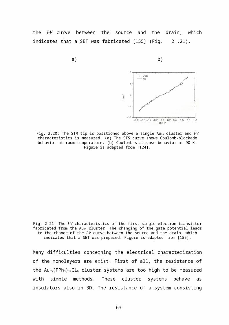
5 Results and discussion of the electrical properties of molecularly cross-linked Au55-systems
The clusters can be linked with and separated from each other using different organic lig-
ands. Three kinds of interactions are possible: van der Waals bonds, ionic bonds, and cova-
lent bonds. If the connection between the ligand stabilized metal particles is of Van der
Waals or ionic type the system is called physically linked system. If covalent bonds are
present, the system is called chemically cross-linked system.
The physically linked systems are conventional “ligand stabilized particles”. They are usu-
ally soluble in organic or inorganic solvents, which destroy the link between the particles,
and after that the clusters are recrystalisable in quadratic and hexagonal microcrystals.
The chemically linked systems are usually more rigid than the physically linked ones, usu-
ally not soluble at all, since “space polymers” are inside. They cannot be chemically ma-
nipulated and build mainly microcrystals with a hexagonal network.
The synthesis of the physically linked systems is summarized in chapter 2.4.5.5.
5.1 Sample preparation
The possible synthesis techniques for covalently and physically cross-linked systems are
discussed in chapter 2.3.4. The experimental descriptions of the synthesis of Au55 systems
is introduced in chapter 8.5 and 8.6. In the following chapters, the problems, and the dis-
cussion of the synthesis methods will be presented.
5.1.1 Preparation of layers
Quasi-one-dimensional structures of physically cross-linked systems were prepared by us-
ing a very diluted aqueous cluster solution of 15 nm gold colloids. This solution was
dropped onto a quartz platelet, and the solvent was let to evaporate (for details see chapter
8.6.1.1). With this technique so-called “dropping circles” are gained (Fig. 5.9). These
structures were contacted with conducting silver spots at different distances (50 and 75
m).
65
Fig. 5.9: SEM image of a thick dropping circle on an EBL fabricated sample.
The detailed preparation of mono- and multilayers of Au55 is reported in chapter 8.6.
Quasi-two-dimensional structures of physically cross-linked systems can be obtained with
the same method, but with the use of much concentrated solution. Disadvantage of this
method, that the thickness of the sample is not homogeneous. To get flat surface spin coat-
ing technique has to be used (see Fig. 5.24).
Physically and chemically cross-linked monolayers can be obtained with the use of the LB
technique (see chapter 2.4.5.3). In this work for the preparation of Au55(PPh3)12Cl6 mono-
layers a dichloromethane solution of normal Au55 was dropped onto aqueous PVP solution
containing already a substrate dipped inside. After evaporation of dichloromethane, the
layer was transferred to the substrate, (cover-glass (8x8 mm), or any other sample), with
pulling it out from the liquid. With this technique islands of closed Au55 monolayers could
be obtained (Fig. 5.10).
The use of the same method in the case of a carbon coated TEM grid resulted in large areas
of ordered cluster structures (up to 1 m) (see chapter 2.4.5.3) [139]. It might be also the
case if another substrate is used, if it is assumed, that the substrate doesn’t influence too
much the structure of the layer. This assumption is not very strict, since the arrangement of
the cluster layer is directly influenced by the PVP layer and just indirectly by the substrate.
The truth of this assumption cannot be proved with the available methods, since it cannot
be decided nor with the use of nor AFM or SEM (too small resolution), or with TEM (the
glass substrate is not “transparent” for the electron beam).
66
Fig. 5.10: Monolayer of Au55(PPh3)12Cl6 prepared by a modified LB technique. The height difference between the lighter, and darker regions is about 3 nm, which is equal with a 2 nm high cluster layer, and a 1 nm thick
polymer film underneath.
The physically cross-linked layer can be transformed to a two-dimensional covalent clus-
ter-polymer, with spreading the dithiol solution onto the water surface covered by the
physically cross-linked Au55 layer. The gained arrangement can be transferred onto a sub-
strate with the same method, as before. The AFM and TEM picture of the obtained layer is
showed on Fig. 5.11.
a) b)
Fig. 5.11: Monolayer of a cross-linked Au55 system prepared by a modified LB technique. (a) is an AFM im-age. The height difference between the lighter and the darker regions is 4 nm, which is more-or less equal
with an Au55 cluster core (1,4 nm) with a 1 nm thick ligand shell. (b) is a TEM image. The clusters inside the layer can be observed. There is no evident sign of high range ordering.
67
The monolayers obtained using the LB technique were carried out on a water surface (acid
base catalyst) in presence of oxygen. Using this method, monolayers with oxidized thiol
groups were fabricated (Fig. 5.12).
Fig. 5.12: TEM image of a cross-linked monolayer of Au55 clusters, prepared by LB technique.
As can be observed from Fig. 5.12, the distances between the particles are relative big,
compared to the cluster size. In one TBBT molecule the distance between the two sulfur
atoms is approximately 1 nm, an oxidized TBBT molecule has a length of maximum 2 nm.
In this picture it can be observed, that the distance of the metal cores is larger than their di-
ameters. This implicates that the TBBT molecules are oxidized during the formation of this
rigid film.
Using this method for the preparation, the purification of the sample is wholly impossible,
so there is no information about the residual PPh3 and dithiol in the system.
Monolayer with large closed areas can be also prepared with the silanisation of a substrate.
The so prepared layers contain only covalent bonds. The experiment was divided into 4
steps: a glass substrate was first dipped into a HCl solution and then into 3-chloropropyl-
dimethylsilan-carbamate under N2 atmosphere. After washing the sample carefully with
pentane to remove the excess of the silane, it was heated for making the silane-oxygen
silane bonds irreversible on the surface. The thickness of the silane layer measured by
AFM was smaller than 0.5 nm. Thereafter, the sample was successively dipped in an
ethanol solution of KSH, washed with ethanol, to remove the excess of the KSH, dipped
68

into a Au55(PPh3)12Cl6 dichloromethane solution, and finally washed with CH2Cl2. With this
method a monolayer was obtained with relative big closed islands of clusters (up to 10
m). To cross-link the deposited particles, the sample was dipped into a dithiol solution
and washed with the solvent selected to solubilize the linker used (the solvents list is pre-
sented in Tab. 8.2). The obtained layer is shown on Fig. 5.13.
Fig. 5.13: SEM images of a monolayer of a cross-linked Au55 system prepared by silanization. The right pic-ture is a zoom on a part of the left one. The darker regions show cluster free areas, the lighter ones the areas
covered by monolayer, and the white points show smaller cluster-microcrystals.
In the case of these silanized samples this problem of the purification can take also place,
however, the clusters are stronger attached to the surface by a chemical sulfur-gold bonds,
so they cannot move so easily. They are also bound to the surface, so the solvation of the
excess of the dithiols, and the free PPh3 is an easier problem. On the other hand, an ex-
change between the bound clusters-surface and clusters-thiol groups can take place. This
could bring a reorganization of the clusters arrangement at the surface or the dissolution of
the clusters into the solvent. To minimize these phenomena, the sample was dipped into the
ligand solution 15 min.
Another difficulty with the silanized samples is, that with the use of a multifunctional
silane (like (MeO)3Si-R, with any organic R) a polymerization can occur during the
silanization of the surface. That may cause that the surface becomes more rough, which
makes it difficult to cover it homogeneously with the small Au55 clusters. That is why the
multilayer was synthesized by the use of TMSPCl and for the monolayer-preparation
KDMSPCl was used.
69
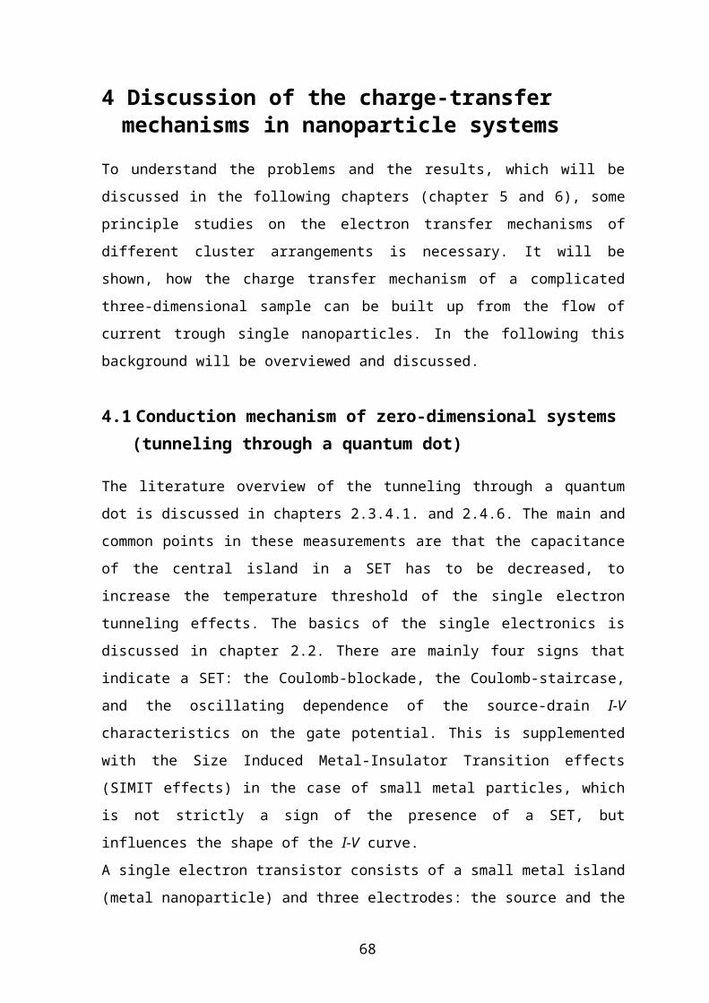
5.1.2 Three-dimensional systems
Three-dimensional Au55 systems were prepared by the one-step cross-linking and precipita-
tion method (chapter 2.3.4.1) [53]. The detailed parameters are presented in chapter 8.5.
In this case, the cross-linker groups used were thiol molecules because of their strong
affinity to the gold core. Cross- linking can take place following two different ways: a di-
rect connection cluster-ligand-cluster, or a cross-link via a S-S bridge in an oxidative
medium, as a cluster-ligand-ligand-cluster connection.
The preparation of an cluster-ligand-cluster connected cluster system was realized under
N2 atmosphere, or without the presence of any acid-base catalyst (hexane as solvent [50]
[51]) to avoid any oxidation. The ligand solution was dropped into the cluster solution. The
reaction was very slow (3-5 weeks). The first step, the exchange of the triphenylphosphine
to thiols, is a fast reaction. This reaction is followed by the the building of the bridges be-
tween the clusters. For this the two ligand shells have to penetrate through each other. This
is a rather time consuming step.
The preparation of the cluster-ligand-ligand-cluster connected systems was realized in the
presence of oxygen and an acid-base catalyst (like water, or DMF). The reaction was rela-
tive fast; it presented the precipitated space polymer in 1-2 hours after the dropping of the
ligand solution into the cluster solution, because of the fast thiol oxidation (Fig. 5.15). It
turned out that traces of water in the dichloromethane is enough for acid-base catalyzing
the deprotonation of the thiols, so the oxidation reaction.
It is also possible to oxidize the dithiol molecules by adding I2 during the reaction. How-
ever, I2 becomes part of the ligands of the cluster-polymer formed and the sample is not
stable enough to be pressed: it becomes metallic. This shows, that if many thiols are ex-
changed by I2, the ligand shell doesn’t protect enough the clusters against the aggregation
and their manipulation is more difficult.
Working with this technique involves two problems: the purification of the sample is diffi-
cult, and the cluster polymer presents chemical non-uniformity. To synthesize and precipi-
tate, the cross-linked systems need just some thiol-Au bonds so some of the thiol groups
still free, even after precipitation of the product. On the other hand, mainly in the case of
the oxygen atmosphere, since the ligands are accessible, an “overoxidation” can take place.
70
which means that between two clusters there are not just two, but more ligands. These two
effects make the determination of the real coordination number of the gold core rather dif-
ficult.
TEM investigations show (Fig. 5.14), that the diameter of the clusters did not change dur-
ing the reaction. The detailed preparation of the three-dimensional arrangements is dis-
cussed in chapter 8.5.
Fig. 5.14: TEM image of (Au55(purine)20)n.
without air with air
Fig. 5.15: Cross-linkage of the clusters, with terminal dithiols. : PPh3, : -SH, : cluster core.
71
5.2 Electrical properties of chemically cross-linked Au55 systems
In the following, the electrical properties of physically and chemically cross-linked sam-
ples will be compared. For the presentation of the results in a wide grasp, results are also
presented, which were not measured in this work. It is tried to give all the citations in its
place, but here at the beginning an overview is presented about this:
- The electrical characterization of the Au55 monolayers was done dur-
ing this work. The only experiment mentioned in chapter 5.2.1 which is not a part
of this work is presented on Fig. 5.22 in chapter 5.2.1.3, which was published in
Ref. [109], and the report of the modification of the LB film in the same chapter,
which was discussed in Ref. [87].
- The electrical characterization of the Au55 multilayers which was
contacted with contacting silver spots was made during this work. The measure-
ments with the use of the EBL fabricated electrode system in chapter 5.2.2 was
published in Ref. [140] and [141].
- The conduction properties of the physically cross linked three-di-
mensional systems was studied by U. Simon, and was published in [114], [129] and
[130]. The Au55 cluster system, which was cross-linked with oxidized hexanedithiol
was also measured by him. Every other measurements was done during this work,
with his support.
5.2.1 Two-dimensional systems
5.2.1.1 Conduction properties of Au55(PPh3)12Cl6 monolayers
Two methods were used to prepare Au55(PPh3)12Cl6 monolayers (for more details see chap-
ter 8.6).
First, the EBL fabricated samples with contact tips (Fig. 8.3) were used to obtain informa-
tion about the electrical properties of the Au55(PPh3)12Cl6 monolayers. However the resis-
tance of the chemically and physically prepared layer was too high to be measured, even
using electrodes less than 20 nm in distance (for details see chapter 6).
72
As a second trial comb structures were used (Fig. 8.5). With this method both chemically
and physically prepared samples could be measured. Three different electrode systems
were used: it was found that the resistance decreased with the increasing of the electrode
area (Fig. 5.16).
Physically prepared layers:
Fig. 5.16: I-V curves measured on a sample prepared with LB technique on three different comb structures: ―: A, ―: B, ―: C (The letters refer to those in chapter 8.7.1.2).
In Fig. 5.16 a very high nonconducting gap can be observed. Coulomb-blockade behavior
is expected in the I-V characteristics of monolayers (see chapter 4.3.3 and 4.5.1), but this
gap is too large to be explained by Coulomb-behavior (see chapter 2.2). In the sample,
small islands of closed packed clusters are present. At the island-boundaries, the conduct-
ing paths have quite high activation energies: these might be an explanation to the lack of
the Coulomb-blockade. That means that, in the case of physical layers, the I-V characteris-
tics of the sample depends on small architectural differences. These differences can be
caused by different island structures (which are not so easily visualizable by SEM, but eas-
ily observable in the quantitative analysis of the measured I-V characteristics), or some
73
contamination on the surface (Fig. 5.17). The asymmetrical localization of this contami-
nates can lead to asymmetrical I-V curve.
a) b)
Fig. 5.17: A SEM image of a comb structure with architectural mistakes (a) and the I-V curves measured on a sample prepared with LB technique (b).
Chemically prepared layers:
The layers prepared by silanization of the EBL fabricated sample are robust. It is also pos-
sible to use this kind of substrate to build up closed-dense packed islands on the microme-
ter scale (Fig. 5.13) The presence of these big islands were demonstrated also by the I-V
characteristics, with an evident presence of smaller a gap than the physically prepared lay-
ers (Fig. 5.18). The non-linearity of the curve may be caused by the different current paths
(see chapter 4.3.2)
a) b)
Fig. 5.18: A SEM image of a comb structure with chemically prepared layer (a) and the I-V curves measured on this sample (b).
74
5.2.1.2 Conduction properties of chemically linked Au55 monolayers
After the deposition of both types of layers onto a substrate, the samples were dipped into a
solution of TBBT. Different behaviors in the I-V characteristics were observed
Physically prepared sample:
Fig. 5.19: I-V curves measured on a sample prepared with LB technique ■: before and ■: after dipping it into the dithiol solution.
During this dipping procedure, some Au55-clusters, weakly bonded to the surface, can be
dissolved back by the dithiol ligands. On the other hand, if the polymerization of the dithi -
ols is fast enough, it will stay on the surface because of its big molecular weight and form a
thin film. Surely both reactions happen statistically, but the resulting I-V characteristics
show smaller resistance than the non-polymerized cluster system, in spite of the probably
smaller number of the clusters on surface (Fig. 5.19).
An alternative to this method was to try to cross link the layer before its transfer onto a
substrate, using the LB method (see chapter 2.3.4.2 and 8.6.1.2). A dichloromethane clus-
ter solution was spread onto a water surface and after evaporation of the solvent, an ethyl
acetate solution of dithiol was added. The choice of this second solvent was governed by 3
parameters: insolubility of Au55, not miscible with water and has a smaller density than the
75
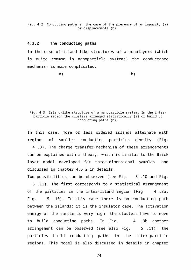
water. The solvent used was ethyl-acetate (EtAc). After evaporation of the EtAc, the sur-
face was compressed and transferred onto the EBL fabricated sample (see chapter 8.6.1,
Fig. 5.11,).
Fig. 5.20: SEM image of a sample prepared with the cross-linker LB technique. The black regions of the sample are the cluster islands. On the left side of the picture a contact pad can be observed.
Because of the shape of the cluster islands (they look like more like a network and not like
islands) (Fig. 5.20) the probability to find a good area between the contact tips was quite
small, and the resistance of such layer was not measured.
Chemically prepared samples:
The particles in the silanized monolayer are not mobile; they are sticked to the surface by
strong chemical bonds (Fig. 5.21). The changing of the resistance in this case is much big-
ger than by the physical layers. The resistance is one order of magnitude smaller by the
cross-linked layer.
76
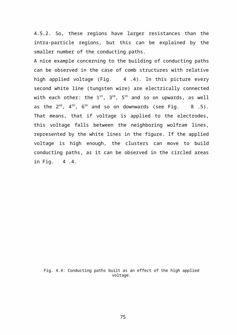
Fig. 5.21: I-V curves measured on a sample prepared with silanization ●: after and ■: before dipping it into the dithiol solution. On the inserted figure the magnification of the curve measured before dipping into the
dithiol solution can be observed.
5.2.1.3 Comparison and discussion
A Coulomb blockade effect was measured by Reifenberger and coworkers in the case of
bigger gold clusters [109]. They have shown that there is a direct dependence between the
chemical properties of the ligands and the current-voltage characteristics. (Fig. 5.22)
Effectively, a layer with clusters separated from each other by two ligand shells, presents a
higher resistance than a layer containing particles covalently cross-linked. Two explana-
tions concerning this phenomenon are possible (Fig. 5.22): the linker molecule with a con-
jugated system supports the electron transfer, or it is induce a smaller distance between
the particles in the cross-linked case.
77
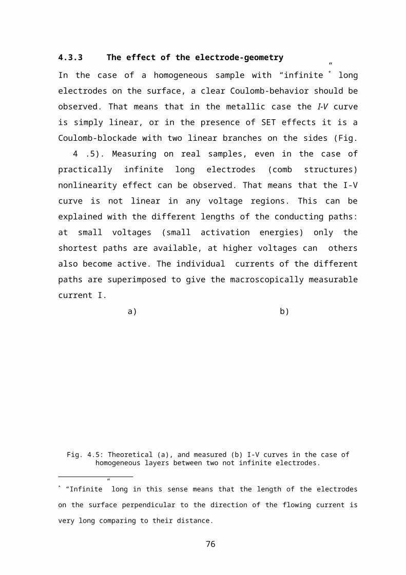
Fig. 5.22: The dependence of the I-V curve on the chemical properties of the ligands. Figure is adapted from [152].
The difference between the covalently cross-linked and the van der Waals bonded clusters
were also investigated in the case of a LB film, where the particles were cross-linked by
dipping a LB monolayer into a dithiol solution [87]. It was found that the resistance be-
comes smaller, if the gold particles are interconnected with dithiols. Nonetheless, the
length of the dithiols used in this work was smaller than the length of the two ligand-shells,
so the smaller resistance obtained cannot be attributed only to the presence of the bridge
ligand. Because of the experimental procedure, the lower resistance can also be a result of
a possible rearrangement, which occurred during the dipping process. In the worst case
even multilayer can be formed.
The same phenomenon was observed also in the case of Au55 clusters (see chapter 5.2.1.1
and 5.2.1.2), but in this case, the length of the ligands (ox. TBBT is approximately 2 nm)
was longer than the ligands of the not cross-linked molecules ( two PPh3 ligands 0.7 nm).
78
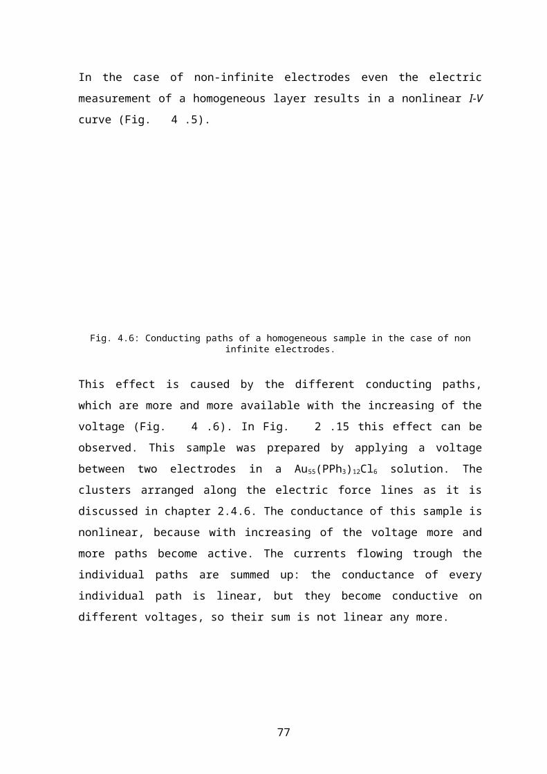
5.2.2 Quasi-one and Quasi-two-dimensional systems
5.2.2.1 Conduction properties of quasi-one-dimensional gold colloid systems
The detailed preparation of such systems made of citrate stabilized gold colloids with a di-
ameter of 15 nm is discussed in chapter 5.1.1 and 8.6.1. The measured I-V curves exhibit a
simple Debye semicircle (Fig. 5.23), which shows that the system contains easy paths for
the electron transfer. The non-metallic behavior of the system indicates that the arrange-
ment of the colloids is not ordered, so the conductance has to occur through easy paths.
a) b)
c) d)
Fig. 5.23: The impedance of the quasi-one-dimensional systems built up from 15 nm gold colloids.
79

It is clear to be seen, that the conductance of the wire depends linear on the cross section: a
sample with a 8 to 6 times bigger cross section (8-12 and 1-2 m2) has a 7 times bigger re-
sistance (see Fig. 5.23 c and d). The conductance varies exponentionally with the distance
between the contacts: the 1.5 times longer wire (50 and 75 m) has a more than a magni-
tude bigger resistance (see Fig. 5.23 a and b).
5.2.2.2 Conduction properties of Au55(PPh3)12Cl6 multilayers
The samples for these measurements were prepared by spin coating technique (see chapters
2.4.5.4 and 8.6.1, Fig. 5.24). The as-fabricated films are not crystallized and usually not or-
dered (Fig. 5.24).
Fig. 5.24: Spin-coating technique. A quartz platelet is spinning with a certain speed and a cluster solution is dropped onto its surface. On the right side of the schematic features of the obtained film can be observed.
Wybourne and coworkers [140][141] measured the I-V characteristics of three types of 50
nm thick films prepared by spin-coating technique from Au55(PPh3)12Cl6 (Fig. 5.25). After
measuring the I-V curve of the sample, they exposed it to an electron beam having 40 keV
energy.
As a third experiment a layer of gold clusters stabilized by octadecanethiol (prepared by
ligand exchange reaction from Au55(PPh3)12Cl6) was spin coated onto a substrate. The I-V
characteristics of all three samples can be observed in Fig. 5.25 b.
80
a) b)
Fig. 5.25: (a) Optical image of nanocontacts 15 m from each other, fabricated with EBL. Between the elec-trodes there is a 50 nm thick film prepared with spin coating technique from different types of Au55 clusters.
(b) I-V curve of this system, using: ●: Au55(PPh3)12Cl6 clusters, ♦: octadecanethiol stabilized Au55 clusters, ▲: Au55(PPh3)12Cl6 clusters exposed with 40 keV electron beam. Figure is adapted from [140] (a) and [141]
(b).
It is clearly recognizable that the electron beam “activates” the cluster system. The resis-
tance of the irradiated samples is smaller than the non-irradiated ones. On the other hand,
the authors experienced a higher stability of the irradiated samples. According to the au-
thors, the increased conductance is the result of a cross-linking mechanism between ligand
shells, which lock the cluster cores better to their places.
The authors reported, that on Fig. 5.25 b Coulomb-blockade can be observed in all three
cases. In the non-exposed cases, a value of the gap of 60-100V is observable: this one is
too high to be a Coulomb blockade (see chapter 4.1 and 5.2.1.1).
Thicker layers of Au55(PPh3)12Cl6 clusters were investigated during this work. The detailed
preparation of them is discussed in chapter 8.6.1 (Fig. 5.24). The I-V curve measured at
different temperatures show linear behavior from 300K down to 150K (see chapter 4.5.3
and Fig. 5.26 ).
As it can be observed the Arrhenius curve is almost linear in this temperature region, so the
granular model doesn’t fit better in this case. The activation energy of the 300 nm thick
layer is 0.20 eV, and in the case of the 500 nm thick layer 0.18 eV (see chapter 4.4).
81

a) b)
c) d)
Fig. 5.26: I-V curves measured on 300 (a) and 500 (c) nm thick layers, and the temperature dependence of the conductivity of the 300 (b) and 500 (d) nm thick layer.
The Impedance of the same samples show clear Debye behavior, and the resistance was in-
dependent from the applied voltage (Fig. 5.27). This sample seems to follow the classical
Ohmic law of the conductance. This fact indicates that the layer contains many easy paths,
or, in other words, the clusters are arranged in a highly crystallized order (4.5.2). This as-
sumption is confirmed by SEM images (Fig. 5.28).
Comparing the work of Wybourne [140][141] with the 50 nm thick layer, and the other
with the 500 nm thick layer it can be concluded that the 50 nm thick sample gives an I-V
curve more similar to those of the monolayer ( see chapter 5.2.1.1, and compare Fig. 5.16
and Fig. 5.25), whereas the I-V characteristic of the thicker layer is similar to the three-di-
82
mensional samples (see chapter 5.2.3.1). For the explanation of this phenomenon see chap-
ter 4.4.
Fig. 5.27: Impedance measured on a 500 nm thick layer of Au55(PPh3)12Cl6 clusters perpendicular to the sur-face. The different colors show different voltages.
Fig. 5.28: SEM image of a sample prepared by the spin coating technique (see chapter 8.6.1).\
83
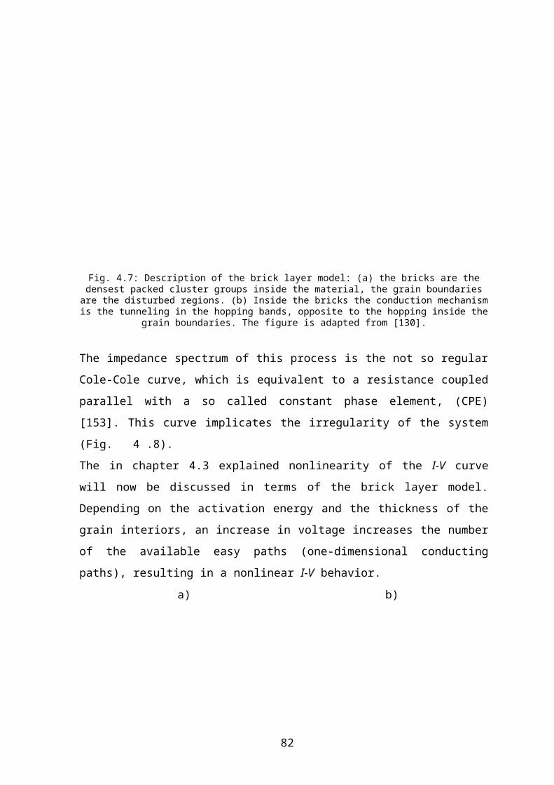
5.2.2.3 Conduction properties of Au55(PPh2C6H4SO3H)12Cl6 multilayers
The detailed preparation of this system is described in chapter 8.6.1 (Fig. 5.24). The water
soluble Au55(PPh2C6H4SO3H)12Cl6 cluster shows different I-V curves compared the normal
Au55, That indicates different conducting mechanisms (Fig. 5.29).
Fig. 5.29: I-V curve of the water soluble Au55(PPh2C6H4SO3H)12Cl6 cluster on different temperatures. The layer thickness is about 500 nm.
In the case of the ligand (C6H5)2C6H4SO3Na, non-linearity effects have been observed.
Two explanations can be imagined for this phenomenon. The first is that in the cluster
layer mobile Na+ ions are present. Together with the residual water in the layer this ions
can act as charge carriers. The second explanation assumes that the cluster layer is not or-
dered. This fact can also be a cause of nonlinear I-V characteristics (see chapter 4.5.2).
Coherent to the I-V measurement, the water soluble cluster systems show a voltage-depen-
dent impedance spectrum.
A decreasing of the impedance with an increasing of the potential U can also be a conse-
quence of the movable Na+ ions, or a disorder in the cluster arrangement (see chapter
4.5.2). The model function, based on to the“ easy path“ theory has been fitted to the mea-
sured curves (see chapter 4.5.2 and Fig. 4.8). The capacitances and the exponent of the
CPE have been found to be voltage- independent, hence the resistances depend on the ap-
plied voltage. This information is not enough to decide between the two possible effects.
84
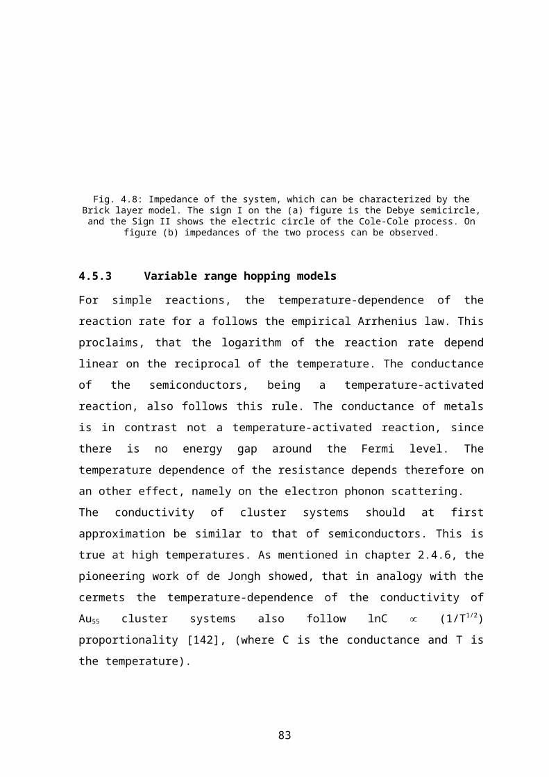
Fig. 5.30: Impedance measured on a 1m thick layer of Au55(PPh2C6H4SO3H)12Cl6 clusters perpendicular to the surface. The different colors show different voltages: 0.0 V, 0.1 V, 0.2 V, 0.4 V, 0.5 V, 0.7 V,
1,0 V. The fitted curves (solid lines, almost invisible) cover perfectly the measured datasets.
5.2.2.4 Conduction properties of chemically cross-linked Au55 multilayers
The detailed preparation of these films is described in chapter 5.1.1, 5.2.2.2 and 8.6.2. The
I-V characteristics of these layers show linear behavior between 300 and 90 K (Fig. 5.31).
a) b)
85
c) d)
Fig. 5.31: I-V curves measured on 5 times (a) and 6 times (c) repeated circle (see chapter 8.6.2), and the tem-perature dependence of the conductivity of the 5 thiol-cluster layer (b) and 6 thiol-cluster layer (d) nm thick
layer.
The resistivity of the chemically prepared layers was smaller than in the case of physical
multilayers. The chemical layers , measured in this work, were maximum 50-60 nm thick.
It can also be observed that the Arrhenius curve is almost linear, at least in the case of the
thicker film. With the thinner film a higher nonlinearity is observed. That means that by
means of activation energy calculations, only the higher temperature points have to be
taken into account (see chapter 4.5.3). Here and in the further chapters just the conductivity
data, belonging to temperatures >200K will be used for the determination of the activation
energy. The activation energies of the two samples are: EA5(layers) = 0.043 eV, EA(6 lay-
ers) = 0.039 eV.
The measured impedance spectra show a simple Debye behavior (Fig. 5.32).
Fig. 5.32: Impedance measured on 4 times,(a) 5 times (b) and 6 times (c) repeated circle (see chapter 8.6.2). The different colours symbolise different frequencies. Yellow: 0.1–1 Hz, green: 1-10 Hz, purple: 10-100 Hz,
cyan: 100-1000 Hz, blue: 1000-10000 Hz.
a.)
c.)b.)
86

The simple Debye behavior implicates that inside the samples easy paths to follow the
classical Ohmic behavior are accessible. That means that inside the layer the clusters are
organized in a highly crystalline order (see chapter 4.5.2).
5.2.2.5 Comparison and discussion
Three different electrical behaviors were found. In the first (chapter 5.2.2.2) (physical
layer) and the third case (chapter 5.2.2.4) (chemical layer), the layers showed clear Ohmic
behavior, which was explained by a highly crystalline arrangement of the clusters. In the
second case the electric behavior turned out to be different, which may be caused by the
ionic conductance, or the disorder in the film (see chapter 5.2.2.3). The dependence of the
shape of the curve on the range of crystallization is the main similarity between the chemi-
cally and physically prepared layers. Another similar effect is the dependence of the activa-
tion energy on the layer thickness.
The main difference between them is their resistance, and the value of the activation en-
ergy. The covalently cross-linked systems have five times smaller activation energy, than
the physically prepared layers.
5.2.3 Three-dimensional systems
The Au55 was the only nanoparticle, in which case the three-dimensional conductance was
measured and investigated. This is because the resistance of these systems is relative high.
The advantage of the three-dimensional measurements is, that they don’t hold other possi-
ble structural defects as the measuring on two-dimensional arrangements, but they are
more robust. That means that they are not so sensitive for small changes in the synthesis
parameters and the stochastic effects, than the two-dimensional arrangements. Also, the
number of the conducting paths is larger, so architecture problems don’t play as a big role
as in the case of the monolayers.
87
5.2.3.1 Conduction properties of physically cross-linked systems
One of the most important questions in this field was to investigate, how the activation en-
ergy of the electron transfer depends on the chemistry and the size of the ligand shell. This
work was done mainly by U. Simon et. al. [114][129][130][144]. They measured the tem-
perature-dependence of the conductivity in compressed pellets of clusters, stabilized by 9
different ligands: PPh3, PPh2C6H4SO3H, P(C6H4CH3)3, P(C6H4OCH3)3 [129], T8-OSS [121],
BOS [122] (Fig. 2.13), and the Au55(PPh2C6H4SO3H)12Cl6 cluster, linked with different
spacers, like DDE, BATA and POB [114], [143] (Fig. 2.19). The temperature-dependence
of the conductivity of these 9 ligands indicates mainly three different rules: the very first
results [129] showed a charge-transfer kinetics depending mainly on the small disorders in
the material. The second measurements with different spacers denoted to a correlation be-
tween the distance of the cluster cores and the activation energies [114], [143]. The investi-
gations with the sulfide ligands show, how the strength of the organic backbone effects the
conduction mechanism [143].
In Ref. [129] results are summarized on the mentioned ligands. The authors pressed the
powder of the cluster sample into small pellets, and compared their density to the theoreti-
cally calculated one. They measured also impedance to obtain information about the kinet-
ics of the reaction. The results show that two elementary reactions exist. They calculated
the activation energy for both reactions in the case of all three particles. The results show
that the disorder rate of the pellet influences the activation energy. In Ref. [130] the au-
thors explain the measured phenomenon. According to this theory in the sample, closest
packed islands are separated with slightly disordered regions (see chapter 4.5.2).
Measuring the temperature-dependence of the charge transfer of the Au55(PPh2C6H4-
SO3H)12Cl6 cluster, linked with different spacers, it was observed that the activation energy
doesn’t depend on the chemical properties of the spacer, just on the distance between the
metal cores [114].
As a next step the PPh2C6H4SO3H ligands were exchanged to T8-OSS and BOS (see Fig.
2.13). With this change the coordinative bonds on the surface of the cluster core were ex-
changed from a Au-P bonds to Au-S interaction. This means a difference in the electron
88
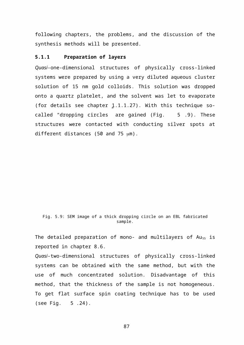
configuration of the formed complex. In spite of this, the charge transfer behavior of the
cluster system didn’t show deviation from the rule explained before [143] (Fig. 5.33).
Fig. 5.33: The dependence of the activation energy of the conduction from the distance of the particles. The figure is adapted from [143].
The extrapolation of the activation energy for a 0 nm distance (Fig. 5.33) ) gives a value of
0.137 eV for the charge transfer. This energy is needed for the classical charging of a
sphere shaped capacitor, with the geometrical parameters of our cluster system. The charg-
ing energy of a capacitor depends linear on the distance between the two metallic parts.
Speaking chemically, the activation energy for the disproportion reaction of a cluster pair
depends directly on their distance. The reaction is thermally activated. The mechanism of
the charge transfer is based on this reaction and can be explained by the variable range
hopping models (see chapter 4.5.3).
5.2.3.2 Electron energy levels of the used ligands
As it is explained in chapter 5.1 and 8.5, dithiols were used to cross-link the particles. 4
different ligands were used here both in the non-oxidized and in the oxidized form: TBBT,
Purine, 1,5NDSH, 1.6NDSH (Tab. 8.2). Oxidized forms mean dimerization of the thiol to a
disulfide. The detailed synthesis is described in chapter 8.5.
89
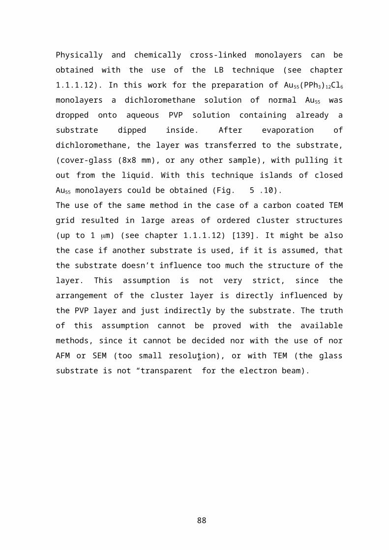
Except for the TBBT, all the ligands used (Tab. 8.2) were rigid and aromatic systems. This
implies a total electron delocalization, even in the S atoms of the thiol groups, which
participate with their nonbonding electron pairs in the delocalization. To prove this,
chemical calculations were made for all ligands used, in order to get an impression from
the value of the HOMO-LUMO gap and to see the degree of the delocalization.
1.5 NDSH OX 1,5 NDSH
Structure
HOMO
LUMO
Tab. 5.1: Structure, HOMO and LUMO orbitals of the !,5 NDSH and the ox. 1,5 NDSH. The different colors show the different phases of the electron wave-function
90
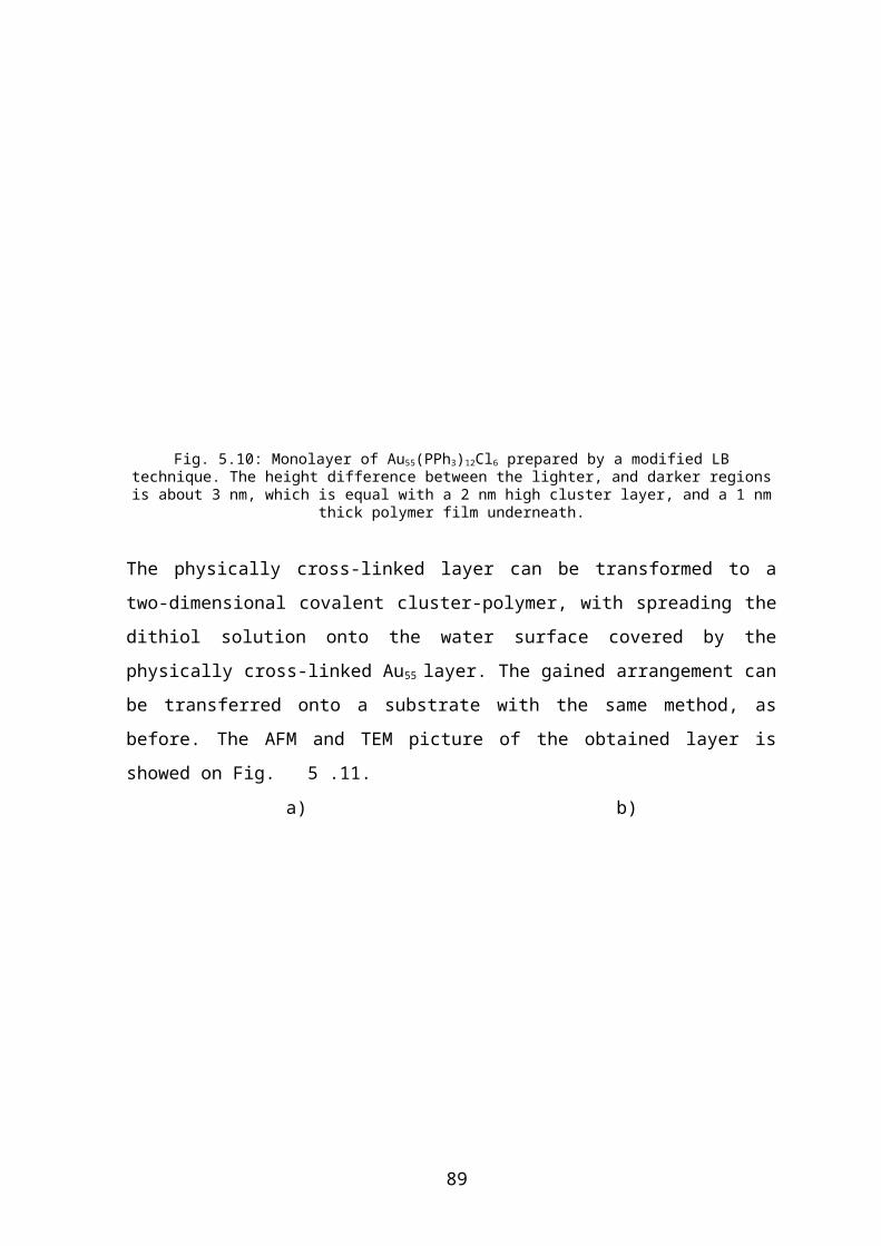
The geometry was optimized by molecular-dynamical calculations; the shape of the wave
functions and their energy was calculated with the semi-empirical Extended Hückel
method. For the calculations the program Hyperchem 6 was used.
As it can be observed in Tab. 5.1 all electrons of the sulfur atoms participate in the delocal-
ization of the electrons. The same effect can be observed in the case of the 2,6 NDSH,
Purine, and all the oxidized forms.
In the case of TBBT, two benzene rings are separated by a S atom, but the electron config-
uration calculations proved that even in this case the energy levels of the molecule show
the delocalization of the nonbonding pairs of the sulfur atom: by this molecule the geome-
try was optimized by Hartree-Fock calculation. The geometry of the wave-function was
also calculated with the Extended Hückel method (Fig. 5.34):
Structure HOMO LUMO
Fig. 5.34: Structure, HOMO and LUMO orbitals of the TBBT. The different colors show the different phases of the electron wave-function
The optimal values of the geometrical parameters of the TBBT are: middle C-S-C angle:
99º, torsion angle between the two phenyl rings (C-S-C-C torsion angle): 87º. The screen-
ing around this values shows that at room temperature almost no change in the C-S-C bond
is available, but the torsion angle can change by 1-2º. If the distance of two terminal sulfur
atoms is investigated then, according to the calculations, the molecule can be claimed as
rigid.
91
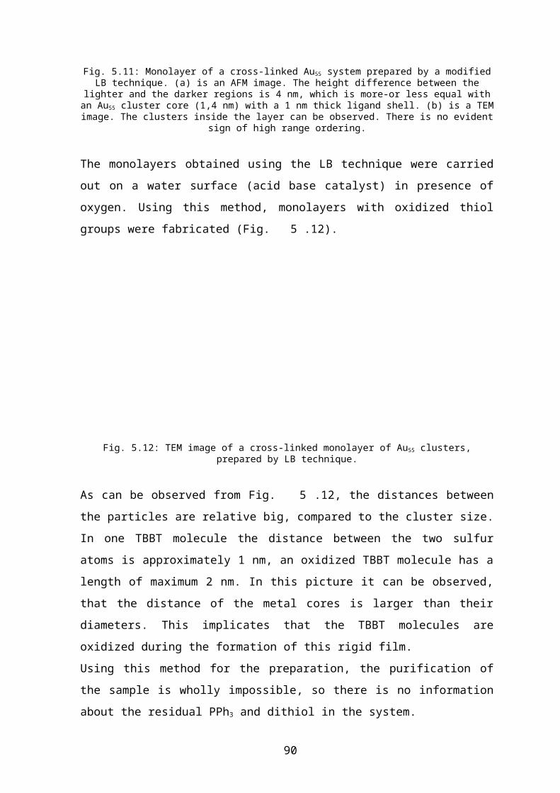
That means that the cluster polymer may preferably form ordered arrangements (Fig. 5.35),
because the molecules keep a constant distance between the clusters. On the other hand, in
an aromatic molecule the electron energy levels are quite close to each other. That means,
that the HOMO-LUMO gap is small. This effect may support the charge transfer between
the clusters.
Fig. 5.35: The structure of TBBT polymerized Au55 cluster system.
The HOMO-LUMO gap of all the molecules, calculated with the Extended Hückel
method, remains <2,5 eV (Tab. 5.2) which also induces the delocalization of the electrons.
TBBT PURINE 1,5 NDSH 2,6 NDSH
normal 2.2 eV 2.3 eV 2.5 eV 2.45 eV
oxidized 1.7 eV 1.9 eV 1.6 eV 1.6 eV
Tab. 5.2: the values of the HOMO and LUMO gap calculated with Extended Hückel model.
5.2.3.3 Conduction properties of chemically cross-linked systems
The temperature dependence of the conductance was measured between 300 and 4 K in the
case of TBBT, and 310 to 77 K for the other molecules. The measured I-V curves are
slightly nonlinear at higher temperatures, but become linear for temperatures less than 230
K. The Coulomb behavior remains up to the smallest measured temperature, 4 K, or 77 K
indicating the existence of a large number of closest packed conducting paths (see chapter
4.5.2).
92
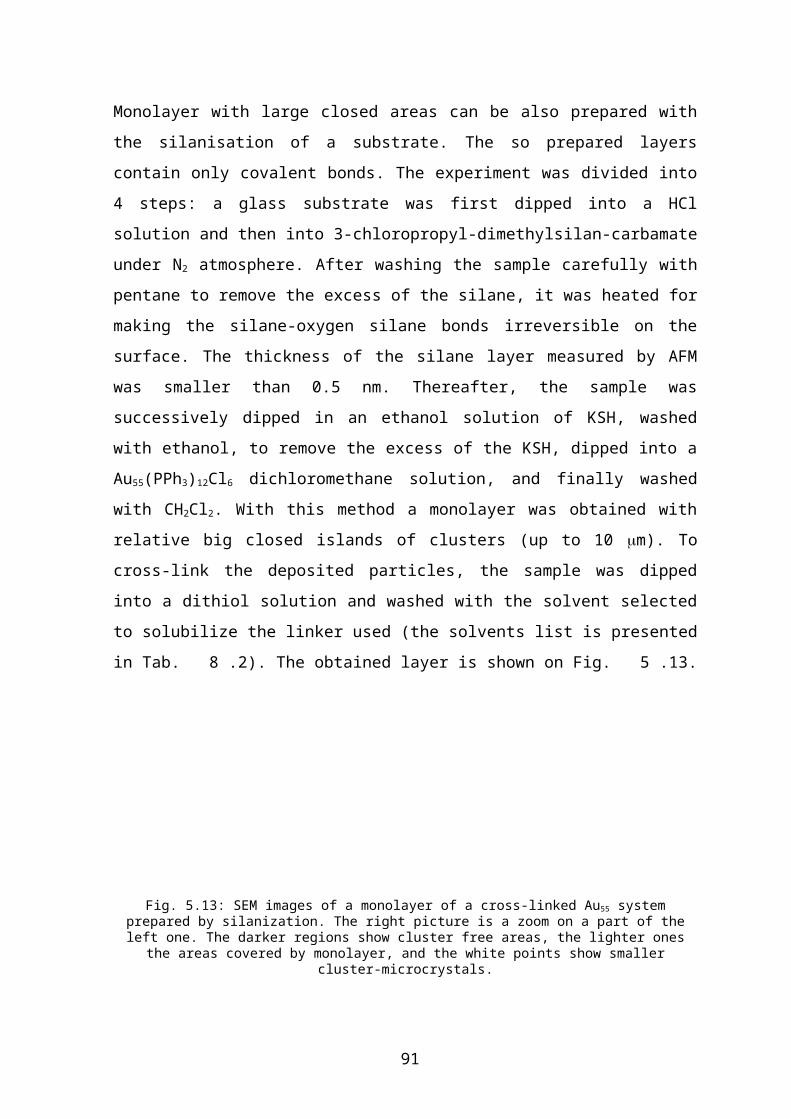
The temperature dependence of the conductivity is not linear, but follows the C 1/T1/2
rule (see chapter 4.5.3) (Tab. 5.3).
Because the Arrhenius equation is not applicable to the whole temperature range, the acti-
vation energy was calculated from the high temperature part of the curves.
In the case of the non-oxidized Purine the curve has a transient behavior. At higher temper-
atures the activation energy is higher than that of every other cluster systems, under the
transient temperature the slope of the curve is in the same region, as those of the curves
usually measured for other Au55 systems. This behavior can be caused by the higher asym-
metric structure of this material, the existence of bigger clusters, or the presence of en-
closed free ligand islands (see Tab. 8.2).
WITHOUT OXIDATION WITH OXIDATION
TBBT
Purine
93
1,5
NDSH
2,6
NDSH
Tab. 5.3: Temperature dependences of the conductance by different ligands.
Impedance spectra were also measured of these systems. Two typical impedance spectra
are shown in Fig. 5.36.
a)
94
b)
Fig. 5.36: Typical impedances at room temperature of the three-dimensional chemically cross-linked sys-tems. The ligands are (a) Purine, (b) TBBT.
The Au55 system polymerized with Purine has the same shape of the impedance, as in the
case of the quasi-two-dimensional samples (see chapter 4.5.2 and 5.2.2): it is probably the
result of a sum of a Debye semicircle and a Cole-Cole process. In the case of the TBBT
polymerized samples the shape of the impedance spectrum is quite surprising, because it
indicating a quite complicated charge transfer mechanism, despite of the apparently or-
dered structure observed in the TEM images (Fig. 5.35). One possible explanation of this
behavior is, that one of the processes showed by the impedance spectrum belongs to the re-
dox process of the central S atom in the TBBT.
5.2.3.4 Comparison and discussion
Spacer Name Distance Ea
TBBT 1.0 nm 0.095 eV
Au55 Au55
95
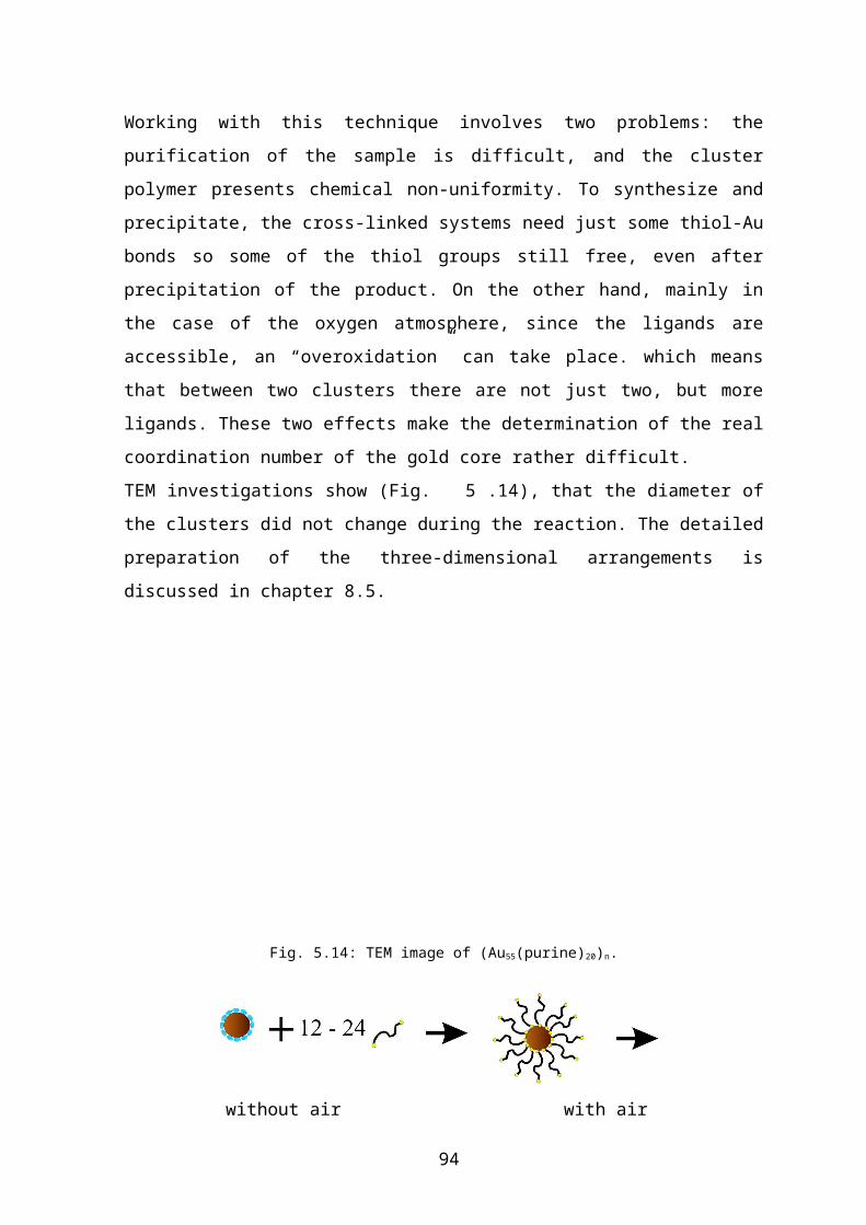
Ox. TBBT 2.0 nm 0.12 eV
Purine 0.7 nm 0.07 eV
(small tem-
peratures)
Ox. Purine 1.4 nm 0.11 eV
1,5 NDSH 0.75 nm 0.064 eV
Ox. 1,5
NDSH
1.5 nm 0.15 eV
2,6 NDSH 0.8 nm 0.17 eV
(possibly
wrong syn-
thesis)
Ox. 2,6
NDSH
1,6 nm 0.14 eV
Au55
Au55
Au55 Au55
Au55Au55
Au55
Au55
Au55
Au55
Au55 Au55Au55
Au55
Au55
96
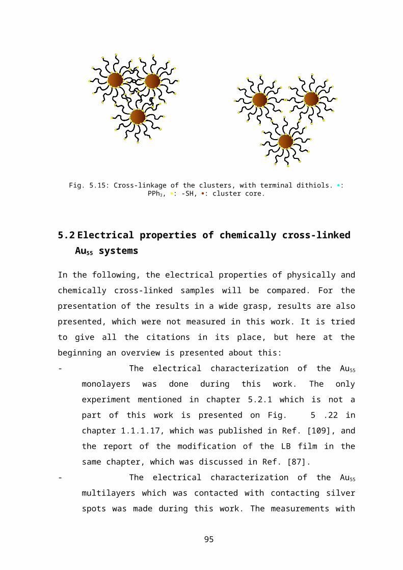
Ox
HexDSH*
1.8 nm 0.15 eV
PPh3* 0.7 nm 0.16 eV
PPh3-
SO3H*
0.7 nm 0.16 eV
DDE* 1.9 nm 0.17 eV
BATA* 2.8 nm 0.23 eV
POB* 3.5 nm
Eff: 1.4
nm
0.20
* The activation energy of this system, together with the not chemically cross-linked systems was measured
by U. Simon [114].
Au55Au55
Au55
Au55
Au55Au55
Au55 Au55
Au55Au55
97
TOS* 3.1 nm 0.26 eV
Tab. 5.4: Conformation and activation energy of different cluster systems and the distance between the clus-ters. █: covalently cross-linked : there is at least one ionic bond between the clusters █: there is at least one
van der Waals bond between the clusters
In Tab. 5.4 are collected the spacers used for all measured ligands, the distance between
the clusters and the activation energy obtained for the systems. The numerical values are
graphically depicted in Fig. 5.37. As it can be observed, the activation energies of the
charge transfer are definitely smaller in the case of the molecularly bridged systems, than
by the not-cross-linked ones.
The effect itself that the activation energy is smaller then it can be expected after the length
of the molecule is not surprising since most of the molecule can be folded, so decreasing
the distance between the clusters. This is well known, and measured in the case of the POB
spacer (Fig. 2.19 c). In this case the inserted -CH2- chains can be folded. The effective
length of the molecule can be calculated from the activation energy of the cluster system
prepared with the use of the Au55(PPh2C6H4SO3H)12Cl6 cluster and the POB spacer [114].
One thing still surprising on Fig. 5.37 is that the activation energy of the cross-linked sys-
tems are smaller, than the activation energy extrapolated for 0 nm distance from the model
explained in chapter 5.2.3.1. This is important because it is a proof that this effect cannot
be explained just by the simple folding of the molecules.
The effect also cannot be explained with the distribution of the electrons between the
HOMO and the LUMO, simply because the voltage drop on one cluster is in the range of
10-6 V, opposite to the STS investigation, in which case it can be up to 4V (see chapter
4.1).
Au55 Au55
98
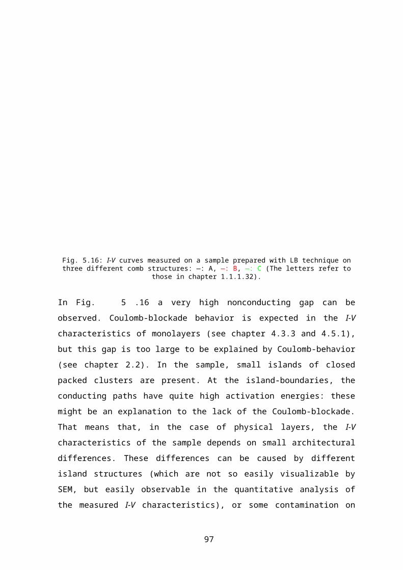
Fig. 5.37: Activation energies vs. the distance between the clusters by different ligands. ■: physically cross-linked systems ●: chemically cross-linked systems. ST means small temperatures.
Inner-sphere and outer-sphere electron transfer mechanisms, reported first by Taube [158],
[159], are well known in the field of aqueous complex chemistry. The theory proposes that
the charge transfer between two, with a ligand bridge connected metal ions, can be up to
108 times faster than without this cross-link. The reason for the smaller activation energy is
that the electrons can use the electron states of the bridging ligand, and don’t need to quit
the inter-molecular space. At cross-linked clusters this mechanism implies that the elec-
trons don’t have to leave the molecule to tunnel between them, but they can move through
a highly conjugated electron system. This effect reduces the activation energy of the charge
transfer between two clusters.
99

a) b)
Fig. 5.38: The mechanism of the formation of the charged cluster pair in the case of the physically (a) and chemically (b) linked system. On Fig. (a) the activation complex is two cluster with an electron outside both
clusters, on Fig. (b) it is two cluster and the electron is somewhere in the ligand sphere.
5.3 Summary and conclusion
It has been shown in the previous chapters that the resistance and the activation energy of
the covalently cross-linked systems are evidently smaller than those of physically cross-
linked ones. This phenomenon may be explained with the generalization of the inner and
outer sphere mechanism from the solution chemistry to all charge transfers between two
particles in any size range. For the two limiting cases the theory was validated thus far: for
atomic/ionic entities the effect was proved first by Taube ([158], [159]) and later by many
others. For macroscopic samples it is also clear that between two metallic bulbs there is a
better electrical contact, if they are connected with a conducting wire. In this work the
availability of the theory for one of the middle size particles was also shown.
100
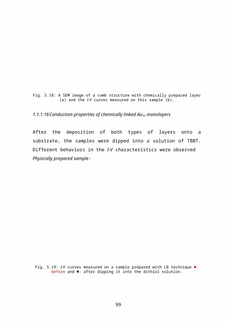
6 Results and discussion of the diode behavior in asym-metrically ordered Au55-monolayers
A diode is originally a heated anode and a cathode in a glass bulb under vacuum (Fig 6-
1.a). If the cathode is positive, the electrons fly through the vacuum, and a certain current,
flowing in the diode, can be measured. But, if the cathode is negative, it repulses the elec-
trons, so they can’t reach this electrode. That is why the original diode rectifies the alter-
nating current and voltage (Fig. 6.1).
a)
Heated anode cathode
b)
Fig. 6.1: Ideal original diode (a), and its characteristic I-V curve (b)
The diode today consists of two opposite doped semiconductor parts. It conducts, when the
n doped part is negative, and the p-doped part is positive. If we apply the voltage in the op-
posite direction, then charge doesn’t go through this circuit element. The n-p junctions in
the today computer technique are really important: every building unit in a chip consists of
different number of this transitions.
Later it was recognized that in every case, when at least two materials with two different
electronic properties are in contact with each other, a small asymmetry in the I-V curve is
observable [157] [132]. The same occurs by almost every STS measurement of cluster or
colloid systems, because the resistance and the capacitance between the tip and the parti-
cle, and between the particle and the substrate, are in general not equal [128][131] ( Fig.
6.2 a). It means, that it is easier for the electron to tunnel through one of the junctions, than
through the others. In this case, the electron movement needs less voltage to flow through
first the smaller resistance, than in the opposite direction. This asymmetry explains the
higher gap at the left side of Fig. 6.2 b. Voltages between the absolute value of the right
101
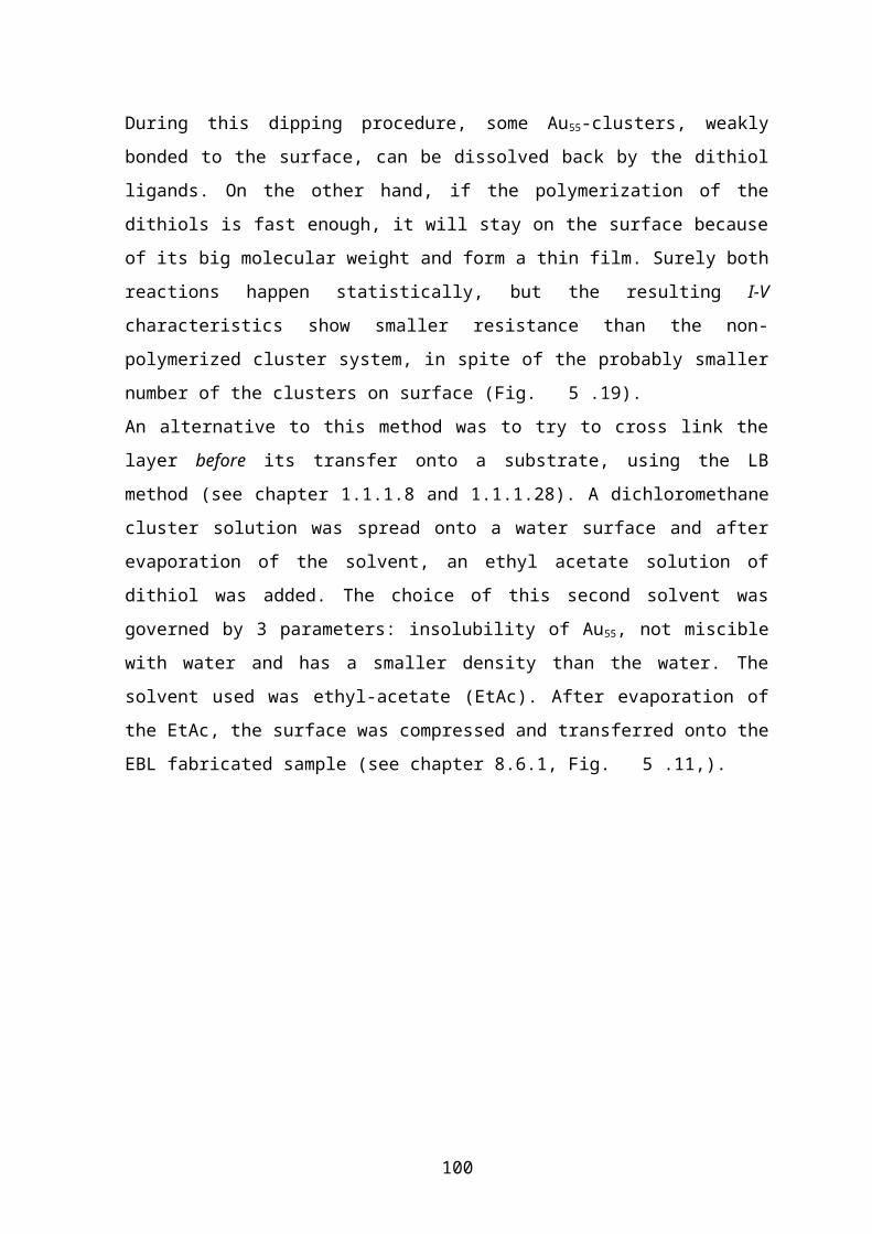
sided and left sided Coulomb-blockade can be rectified, because the system by these poten-
tials let the current flow just in one direction, but not in the other. Of course by STS mea-
surements the position of the tip can be chosen for almost symmetrical I-V curve.
a) b)
Fig. 6.2: a): A schematic description of the double junction system, showing the resistance and capacitance of each individual junction.[131] b): a typical I-V curve, measured above a single cluster[128].
6.1 Asymmetrical multilayers
Fig. 6.3 a shows a SEM image of a Au55 cluster film with a thickness of about 100 nm. It is
clearly noticeable that a drop of water or dichloromethane has flowed between the two
contact tips during the preparation. The leftover material builds an asymmetric arrange-
ment in the layer which has a diode-like I-V curve (Fig. 6.3 b). The asymmetry is about 3
V. That means that for voltages between 3 and 6 V current can flow only in one direction,
but not in the other.
6.2 Sample preparation
For the determination of the electrical properties, a two dimensional arrangement of a
Au55(PPh3)12Cl6 monolayer, prepared by a modified LB technique (see chapter 8.6.1) was
transferred onto a substrate, fabricated by EBL (see chapter 8.7.1.2). The dichloromethane
solutiopn of the normal Au55 cluster solution was dropped onto a very diluted aqueous PVP
solution, which contains the EBL fabricated substrate dipped inside. After the pulling out
the substrate from the solution a monolayer is formed on its surface. Its structure is: the
102
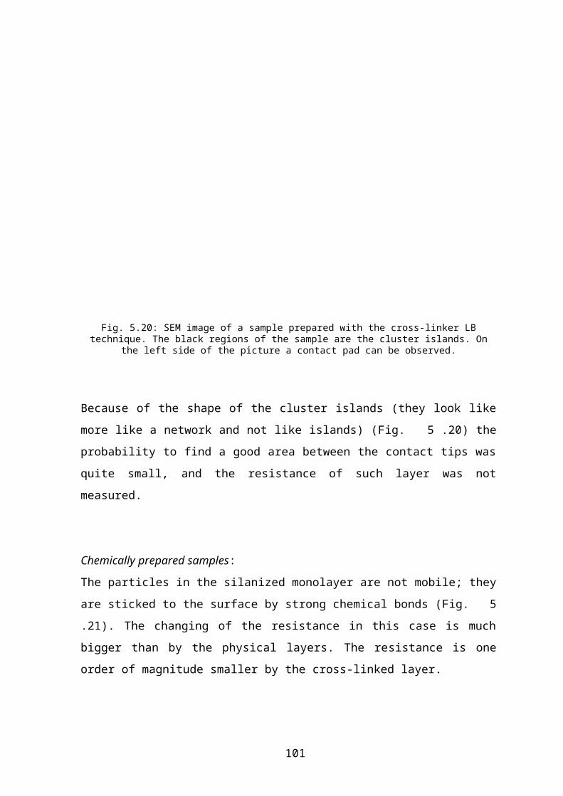
substrate is covered with a thin (1 nm) PVP film. On this film there is a monolayer of Au55
cluster. At least 50% of the surface was always covered by the cluster layer, and with a
good chance that there were also particles between the contact tips (Fig. 6.4).
a) b)
Fig. 6.3: Asymmetrical film arrangement (a), has a diode-like I-V curve (b). The thickness of the film is about 100 nm.
a) b)
c) d)
Fig. 6.4: SEM images of the different cluster arrangements between the contact tips. It is incidentally occurs, if there is nothing (a), between the tips, or just the half of the interstice is covered (b), or there is a cluster is-
land asymmetrically (c) or symmetrically (d) connecting the tungsten contacts.
103
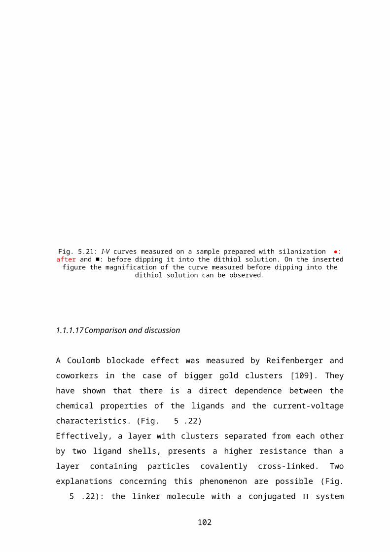
It turned out that the roughness of the sample supports the transfer: effectively the used
surface is very smooth, but some 25 nm high tungsten contact structures are present on it.
With EBL a “smooth-rough surface” can be prepared: there are great smooth areas, namely
on the tungsten and SiO2 surfaces, but the absolute corrugation is 25 nm. This fact seems to
help the monolayer to remain on the surface, in contrast to the too smooth surfaces.
6.3 Activation of Au55 cluster monolayers with electron beam
It is well known, that the electron configuration of the Au55-clusters are in between bulk
and molecule. That means, that their energy levels are quasi continuous, with a small band
gap between the HOMO and the LUMO orbitals [129]. This involves that the Au55 clusters
are similar to semiconductor materials. A silicon platelet can be doped and its conductivity
enlarged, generating holes in the valence band or additional electrons in its conducting
band. To reach this goal in the case of Au55 a monolayer, deposited on a sample made by
EBL, was irradiated with a small energy electron-beam, for 10 s. As it is clearly noticeable
in Fig. 6.5 b, the resistance of the sample after irradiation is at least two orders of magni-
tude smaller than it was before. Other reasons may explain this resistance reduction. One
of them is that during the irradiation, the ligands and the polymer film under the gold clus-
ters can be destroyed, to form a thin carbon film, which is a conductive medium. Another
reason can be in relation with the electron beam: a too long exposition to the electron beam
may diminate aggregation of the clusters. This phenomenon is well known in the case of
TEM measurement. At high energy, a long time irradiation can destroy the sensitive parti-
cles. Finally, in the SEM a thin carbon film is formed: it can disturb the measurement be-
cause it can behave as an insulator, semiconductor, or metallic conductor. Clarke [140]
[141] assumed that the activation phenomenon could be explained with the cross-linking of
the ligand shells. To find the right reason of this effect, some further measurements were
required.
The stability of this activated state was determined (Fig. 6.6). It is clearly observable, that
the probe relaxes. On the other hand, even 39 hours after the irradiation the current is
higher, than before irradiation. A certain nonlinearity of the curves is also noticeable, what
104
is not surprising in the case of these small particles (see chapter 4.3.3). It can be proposed
that after exposure, some rearrangement occurs, working against the activated state of the
layer.
a) b)
Fig. 6.5: SEM image of the Au55-monolayer between the contact tips (a), and its I-V curve (b) before (black line) and after (red line) the irradiation with an electron beam energy of E = 10 keV for t = 10s. The thickness
of the SiO2 layer D = 80 nm.
Fig. 6.6: Stability of the activated monolayer: measurements 0.2 (black line), 15 (red line), 21 (green line) and 39 hours (blue line) after the irradiation (E = 10 keV, t = 30 s, D = 80 nm)
105
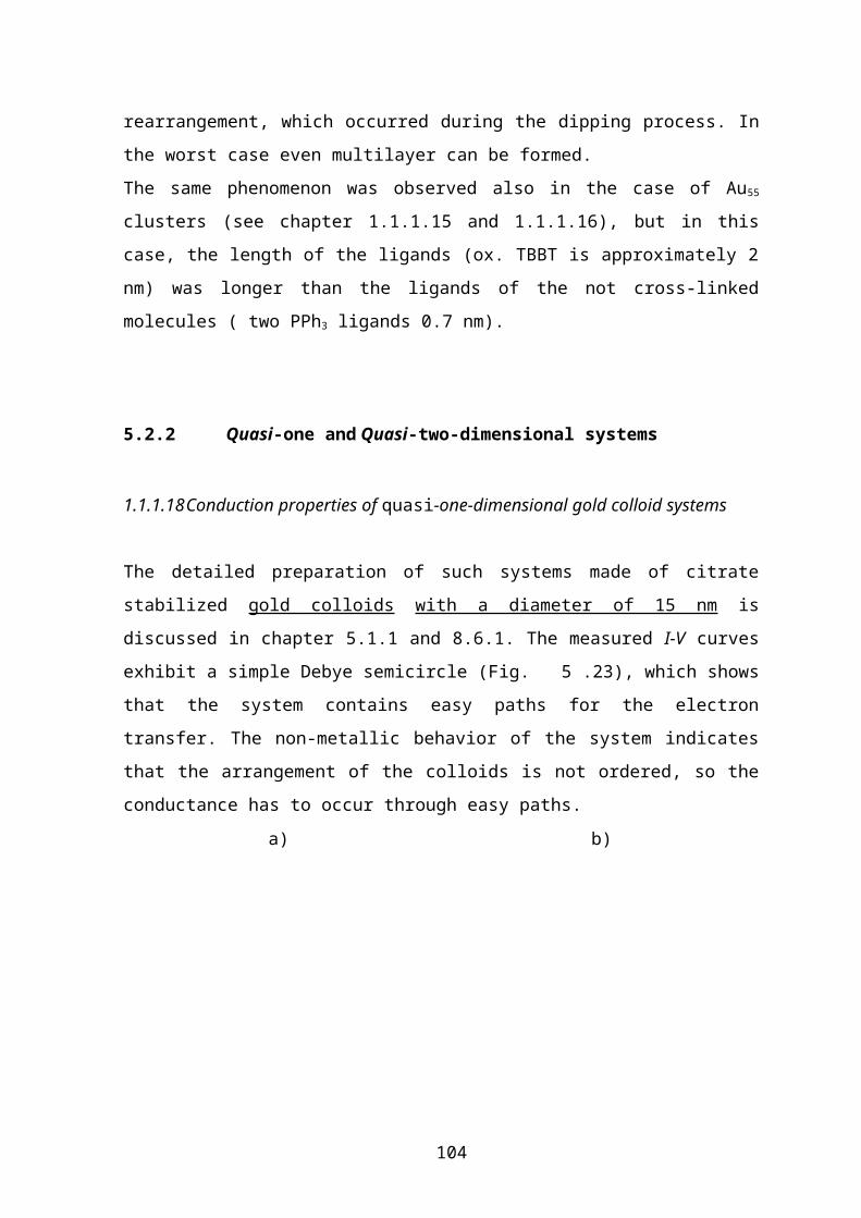
6.4 Preparation of asymmetrically activated monolayers
If the “activation” of the Au55-layer is really a similar effect like the doping of a semicon-
ductor, then the generation of a junction inside the layer (between the two electrodes)
should mean that an asymmetrical I-V curve must be measurable. This experiment is easy
to realize: only half of the interstice of the two contact tips has to be exposed with the elec-
tron beam. In practice it means that the layer is irradiated just around one of the electrodes.
Fig. 6.7 presents an I-V curve measured after exposure with the electron beam for 10 s with
an energy of 10 keV. The asymmetry is about 2 V, which is quite big for this type of sys-
tems. At E = +2 V the current starts to increase. That shows the break down potential of
the “diode”, except that it seems to be reproducible, so the same curve is measurable after
each other on the same system.
Fig. 6.7: Exposure to an electron beam around the left contact tip. (E = 10 keV, t=10 s, D = 300 nm)
This phenomenon excludes all symmetrical explanations of the activation.
106
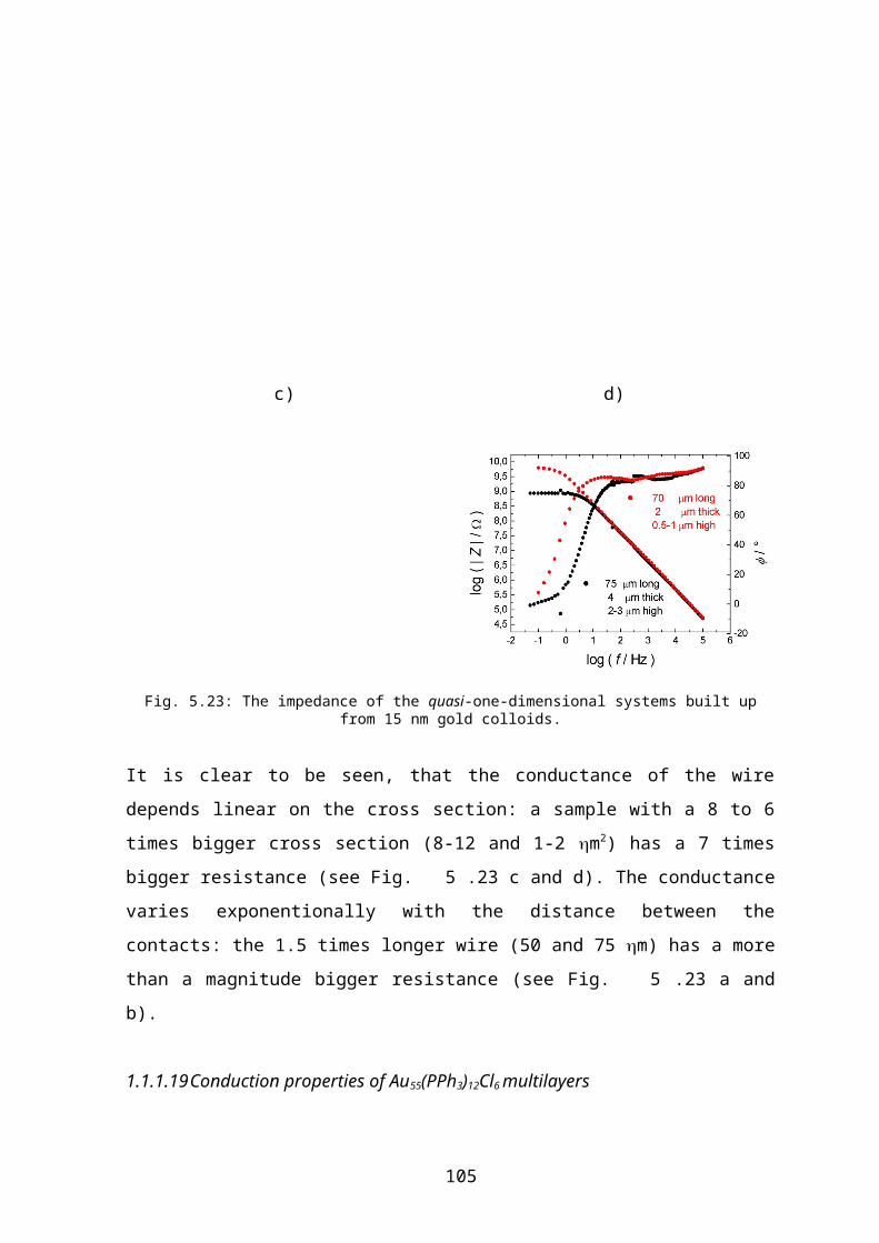
6.5 Properties of asymmetrically activated cluster monolayers
During the characterization of this system, the irradiation parameters were systematically
changed, to find out the optimal energy and time of the exposure, as well as the best thick-
ness of the SiO2 layer. These experiments were also helpful to find out the cause of this be-
havior. The quantitative comparison of the data is not easy, because the value of the mea-
sured current depends strongly on the ratio of the exposed-not exposed area: a too long ex-
position of the irradiated part involves a better conduction, than the other half. It means
that if a larger area is exposed, the resistance of the layer in one direction will be smaller,
and the asymmetry a little higher. Because the electron beam is controlled by hand, and the
sample is continuously drifting, these parameters are not easy to monitor. The voltage
asymmetry is the only measured value, which can be a characteristic of the “diode”, be-
cause it is not very sensitive to the geometric parameters.
6.5.1 The effect of the polymer film
A thin (about 1 nm) and a thick (about 100 nm) film of pure polymer were adsorbed to the
surface, and one tip was exposed to the beam (Fig. 6.8).
a) b)
Fig. 6.8: Irradiation of pure polymer film with electron beam. a: a 1 nm thick film is exposed around the right tip, b: a 100 nm thick film is exposed around the left tip. The black lines shows the I-V curve before irradia-
tion, the red lines after the exposure. (E = 10 keV, t=10 s, D = 80 nm in both cases)
A symmetrical activation is easily observable, but it is not big enough to explain the activa-
tion process of the cluster layer (noted that the polymer layer under the clusters is about 1
107
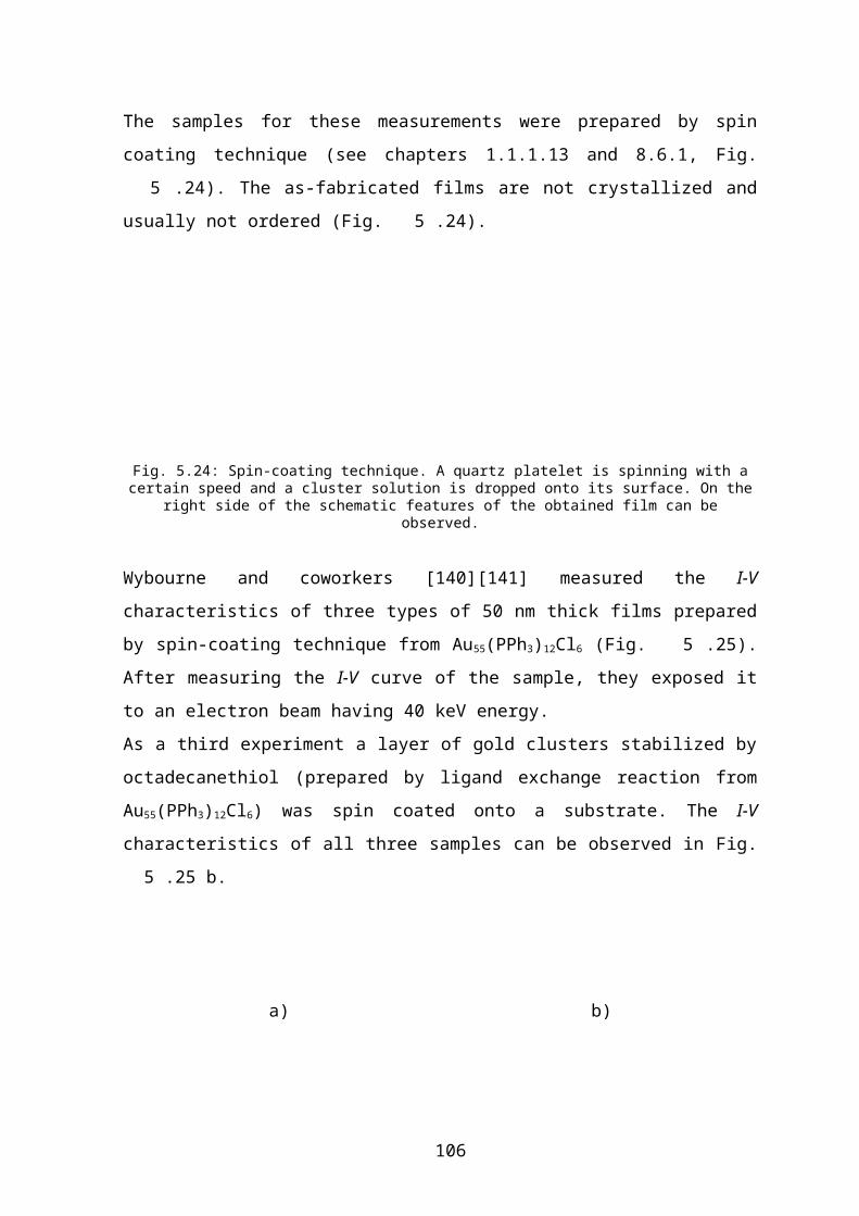
nm thick) (see chapter 8.6.1). The I-V curves of the excited state of the PVP film seems to
be rather an effect of the smaller distance between the electrodes, caused by the reduction
of the polymer film to carbon contaminates, than a doping effect of a semiconductor.
6.5.2 Dependence of the asymmetry on the side of the irradiation
The direction of the asymmetry can easily be changed, because the tungsten structures are
equivalent to each other. If the current is allowed to flow from left to right, then the left tip
has to be exposed, for the opposite direction the right contact needed to be irradiated (Fig.
6.9). On the other hand, this phenomenon also proves that the observed asymmetry is in
connection with the layer and is not an artifact.
a) b)
Fig. 6.9: : I-V curve of Au55 monolayers irradiated around different contacts. a: left tip b: right tip. (E = 10 keV, t=10 s, D = 80 nm in both cases)
6.5.3 Dependence of the asymmetry on the irradiation energy
Fig. 6.10 presents I-V curves of Au55 monolayers irradiated around the left tip, with differ-
ent energies. The hysteresis of the first two curves shows some charging effect, visible, be-
cause of the small measured current. This effect can be caused by a very thin water film
adsorbed on the surface or some other charges remaining inside the substrate. In Fig. 6.10
it is easily noticeable that the asymmetry increases, when the energy of the electron beam
(E) applied is higher: 1 V for E=0.9 keV, 2 V for E = 10 keV, 5 V for E = 16 keV.
108
a)
109
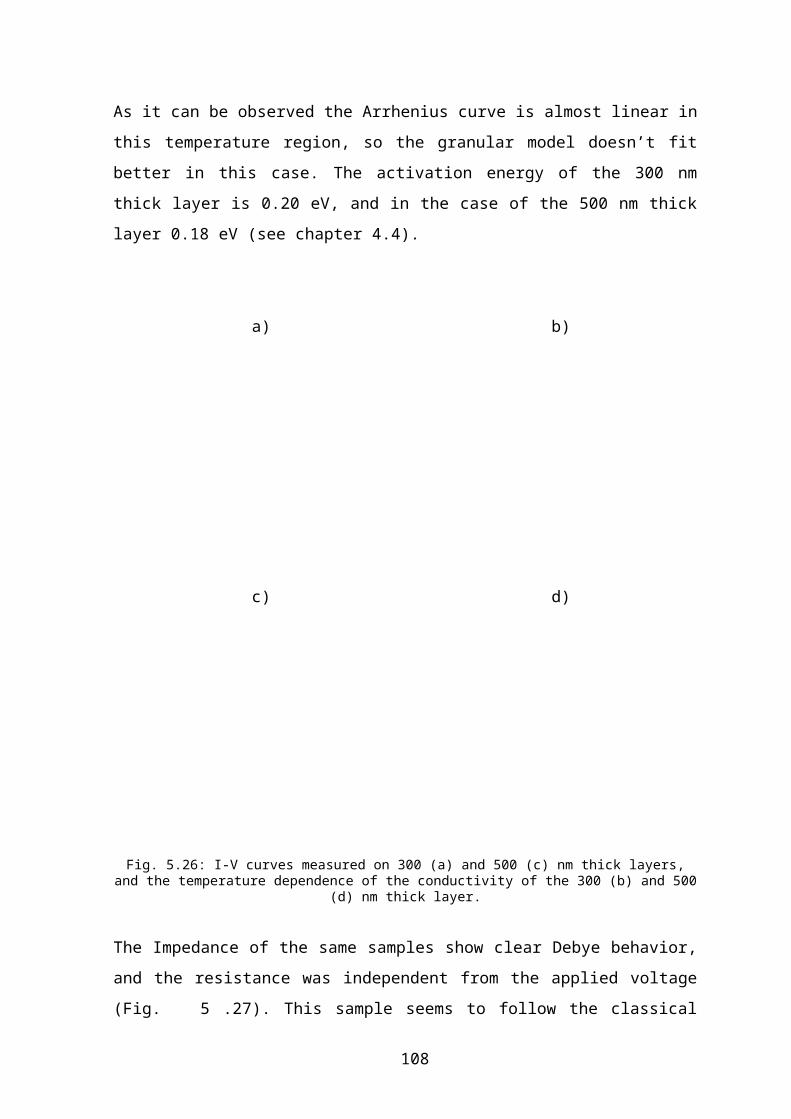
b)
c,)
Fig. 6.10: I-V curve of Au55 monolayers irradiated around the left tip, with different energies of the electron beam. a: E = 0.9 keV, b: E = 10 keV, c: E = 16 keV ( t=10 s, D = 80 nm in all cases)
6.5.4 Dependence of the asymmetry on the irradiation time
a)
110
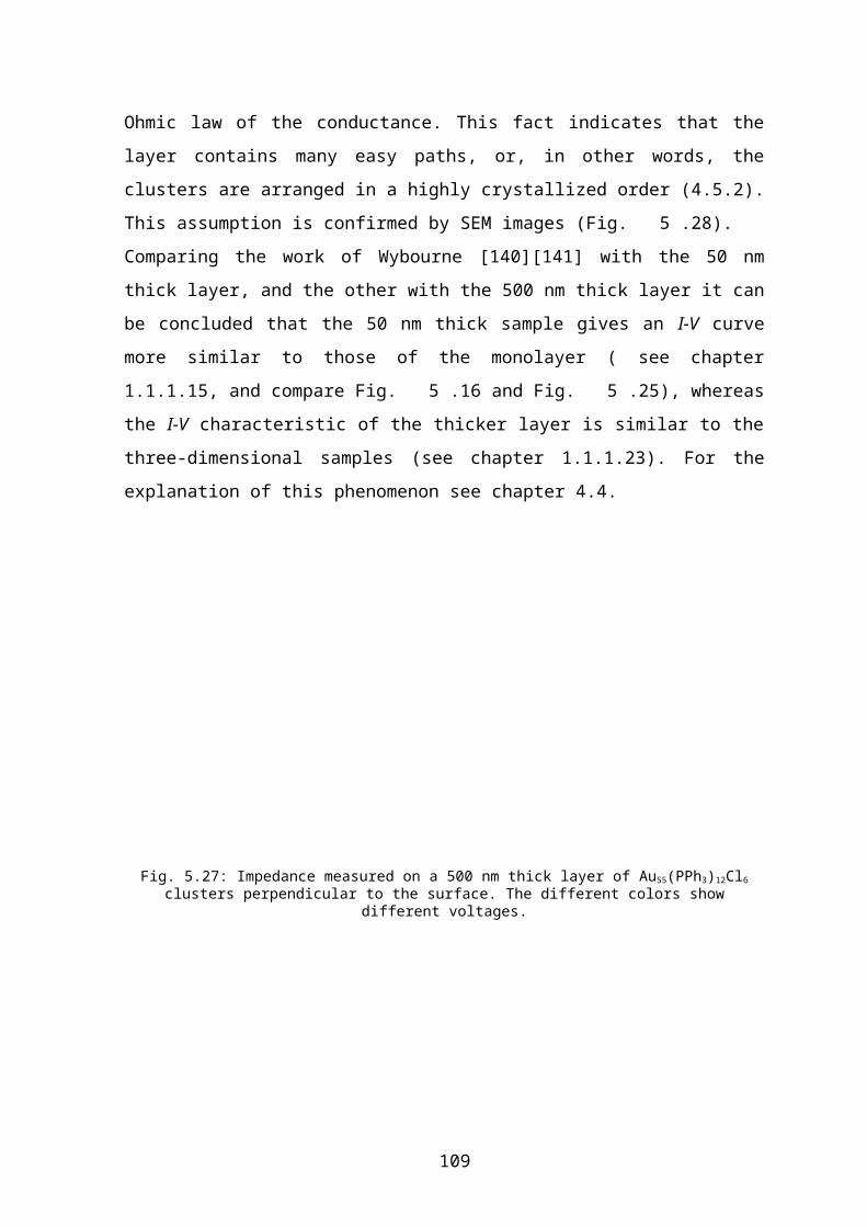
b)
c)
Fig. 6.11: I-V curve of Au55 monolayers irradiated around one of the tips, for different time with a 10 keV electron beam. a: t = 5 s (right tip) , b: t = 10 s (left tip), c: t = 30 s (right tip) (D = 80 nm in all cases.)
111
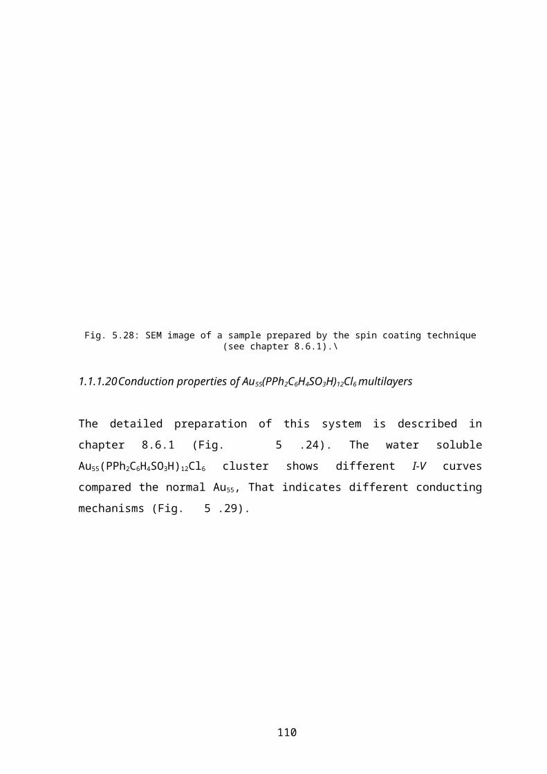
As it can be observed in Fig. 6.11, the time of the irradiation also affects the shape of the I-
V curve. It seems to influence both the height of the gap and the intensity of the active site.
The second sign is quite hard to separate from other effects (see the introduction of chapter
6.5), but the comparison between the current of the activated state and the background cur-
rent give some information. An irradiation of 5s is to too small to get a real effect, and 30s
overactivate the system because a small asymmetry is observed almost without any gap
(see Fig. 6.11 c). The optimal irradiation time turned out to be 10s.
6.5.5 Dependence of the asymmetry on the thickness of the SiO2 layer
a)
b)
Fig. 6.12: I-V curves of Au55 monolayers irradiated around the left tip, on substrates with different SiO2 thick-nesses. (a): D = 80 nm, (b): D = 300 nm, (t = 10 s, E = 10 keV in all cases.)
112
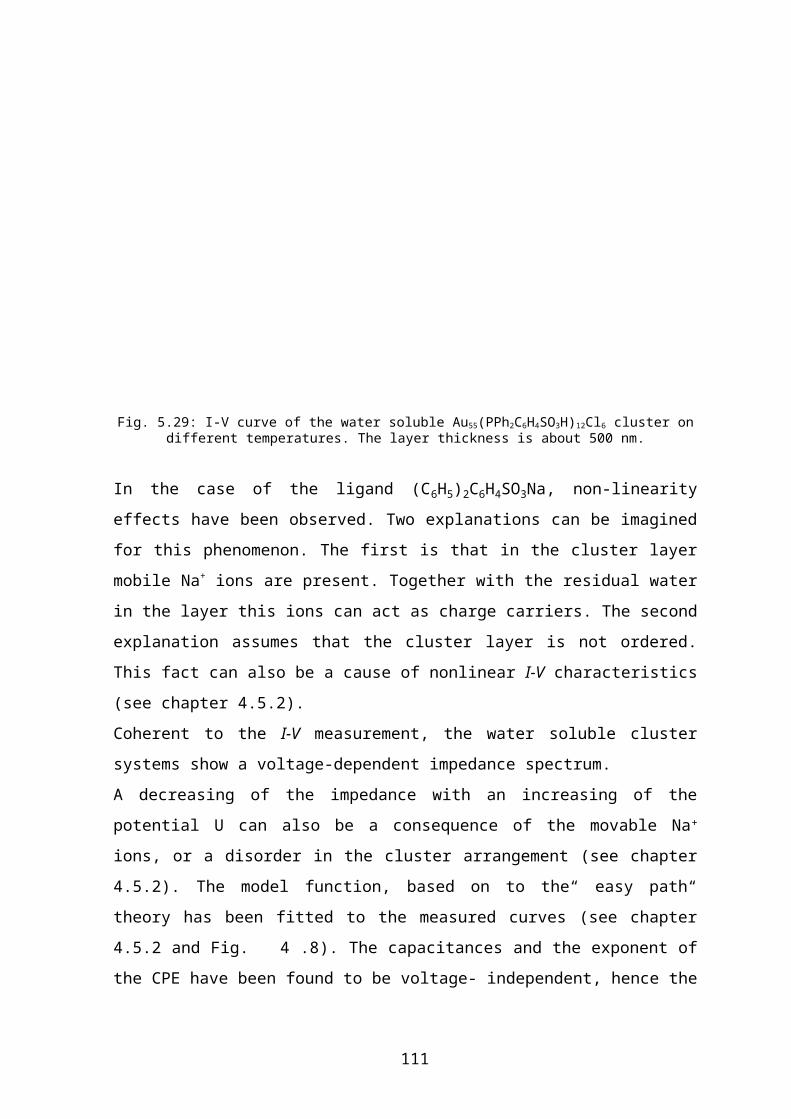
The substrate used consisted of a silicon platelet with an oxidized SiO2 film on it. The
thickness of this layer turned out to influence the behavior of the Au55 layer. This influence
is dramatic: the usual asymmetry of 1-2 V in the case of the 80 nm thick layer increases to
3-7 V with the increasing of the SiO2 thickness to 300 nm. This shows that the effect is in
connection with the substrate-cluster layer interaction. The difference between the two
cases that the conducting Si phase is separated with a thicker isolating gap. This fact makes
more difficult the relaxation of the charges trapped in the top films. This effect also can be
observed on the SEM images, on the smaller contrast.
6.5.6 Relaxation and reactivation process
The activated samples don’t remain activated over one day. They begin to relax. After
some time, depending on the sample, they loose their activated state and become non-con-
ducting. As it will be discussed in chapter 6.6 this phenomenon excludes numerous of the
imaginable explanations. A sample, deposited on a 80 nm thick layer of SiO2 and irradiated
10 s with a 10 keV electron beam, relaxes in the course of 15 hours (Fig. 6.13).
Fig. 6.13: I-V curve of the relaxation process of Au55 monolayers irradiated around the left tip. : 0.2 Hours, 15 hours after the irradiation (D = 80 nm, t = 10 s, E = 10 keV)
113
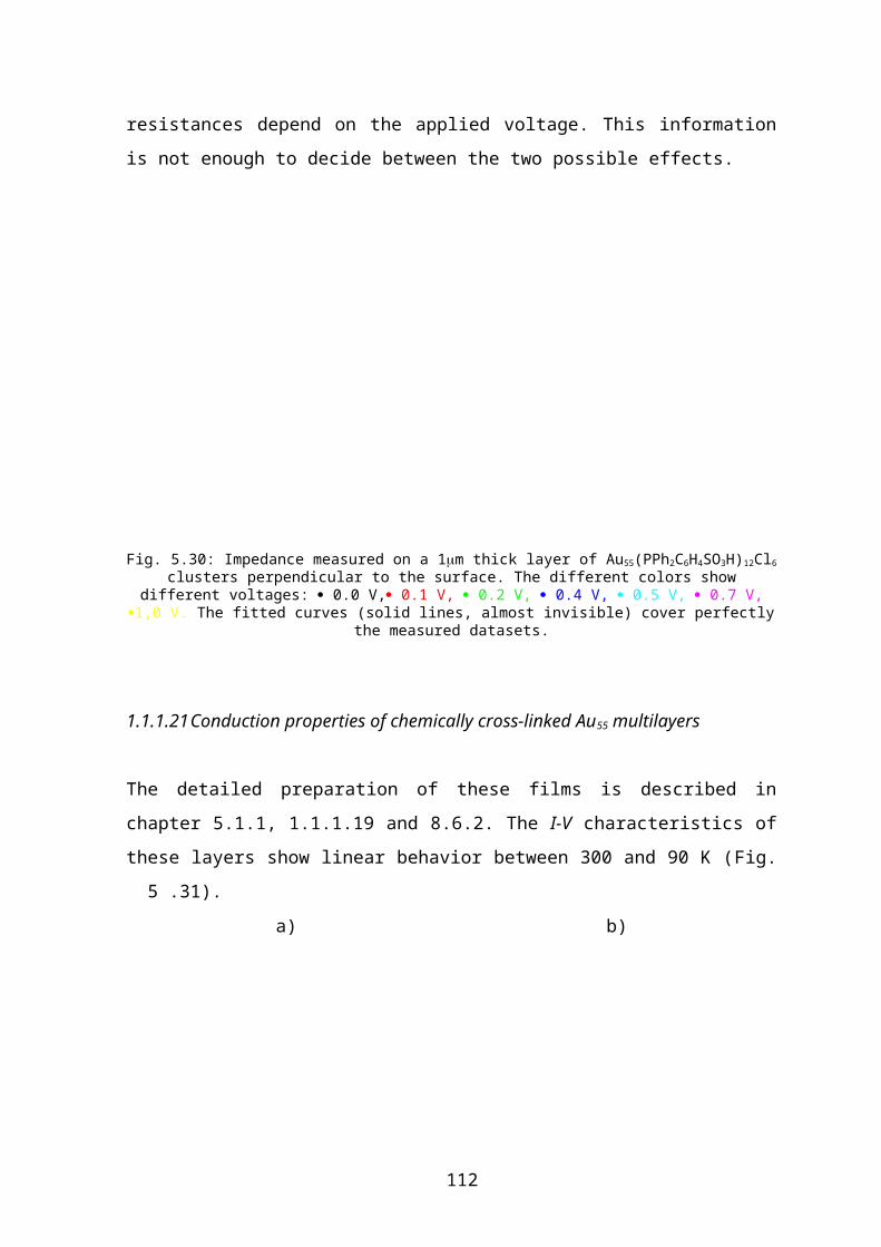
For the samples with 300 nm SiO2 thick films on their surface, the relaxation process is
faster and is reproducible: the layer can be reactivated successively (Fig. 6.14). It is
assumed that the same might occur in the case of the substrates with 80 nm layer thickness,
but it was not measured.
Fig. 6.14: I-V curve of the relaxation process of Au55 monolayers irradiated around the left tip.■: before irra-diation, ●: 0.2 hours, ▲: 7 hours after the irradiation ▼: 0.2 hours after reactivation (D = 300 nm, t = 10 s,
E = 10 keV)
Fig. 6.15: I-V curve of the relaxation process of Au55 monolayers irradiated around the right tip. : 0.2 hours, : 15 hours, , : 21 hours : 39 hours after the irradiation (D = 80 nm, t = 10 s, E = 10 keV)
114
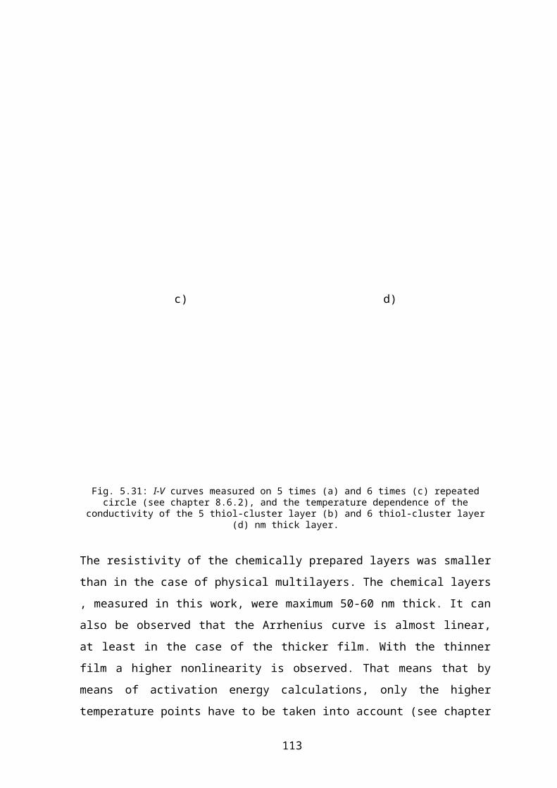
The overactivated sample also relaxes (Fig. 6.15) trough a diode effect, but slower than the
same sample irradiation with a shorter time.
6.6 Explanations and discussion
Many arguments can be considered to explain the activation effect, as well as the asym-
metrical behavior after asymmetrical irradiation:
a) charging effect,
b) aggregation of the clusters and formation of bigger colloids,
c) formation of carbon film contaminate,
d) decomposition of the polymer film, forming a conductor, or semiconductor
layer,
e) chemical reaction inside the ligand shell (for example the cross-linking effects
assumed in Ref. [140] and [141]),
f) the addition to the LUMO or dispossession from the HOMO of charge-carriers
or forming excess of electrons or holes in the material.
Arguments a) – d) would be the “artifactual” explanations, because they are not in connec-
tion with the structure of the cluster layer (see the following chapter). e) and f) points as-
sume structural changes in the Au55 cluster layer, using the properties of the mentioned
nanoparticle.
6.6.1 “Artifactual” effects
In the following paragraphs the artifactual effects will be investigated one by one.
The charging effect can be excluded because the reason of the activation should be a per-
manent effect.
The decomposition of the clusters with concomitant formation of colloids might happen
during the exposition, but this reason is also excluded, because in this case the sample can-
not relax because colloids cannot rebuild clusters under these conditions (see chapter
6.5.6).
115
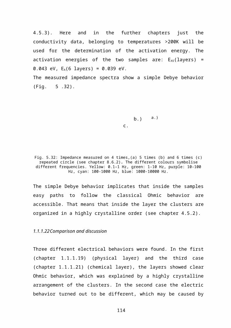
It can be proved with AFM, and light microscopic images, that carbon film contaminate
does form during the exposition. But this reason is also excluded, because it cannot cause
asymmetrical I-V behavior.
The experiments with the thick and thin polymer layer (see chapter 6.5.1) were necessary
to exclude the formation of anisotrop carbon layers. The film in this case was also acti-
vated by the electron beam, but no asymmetrical behavior was observed. The activation ef-
fect, which can be observed on Fig. 6.8 seemed to be rather the effect of the smaller elec-
trode-distance, than the formation of a carbon film.
Another experiment was done to exclude the carbon film contamination effect: blind sam-
ple without any layers was exposed around one of the tips. In this case no activation effect
was obtained.
The logical investigation of the “artifactual” effects showed, that none of them is responsi-
ble for the asymmetrical I-V characteristics of the asymmetrically treated samples.
6.6.2 Structural changes in the Au55 cluster layer
The nature of the structural changes in the Au55 cluster layer will be discussed assuming e)
and f) explanation. The changes of the electron energy levels will be discussed together
with the chemical or structural changes inside the layer.
First, the cause of the rectifying behavior of a silicon-based diode is shown in order to give
an example to the reason of an asymmetric I-V curve.
In Fig. 6.16 the energy diagram of an n-p semiconductor diode is presented. The electrons
in the n doped part of the circuit element occupy some of the LUMO states, so they have
bigger energy. On the p doped part some of the HOMO states are free, so the electrons oc-
cupy smaller energy levels. The Fermi level of the metal contacts are normally situated be-
tween the HOMO and the LUMO of the semiconductor. This situation is shown in Fig.
6.16 a. After applying the voltage, the Fermi level of the negative electrode increases, and
that of the positive electrode decreases. If the n doped part is negative, then the electrons
transit always onto smaller energy levels (Fig. 6.16 b). If the p doped part of the diode is
116
negative, than between the n and p part the electrons have to flow upwards (Fig. 6.16 b),
what is a quite energy consuming step and is allowed just at high potentials.
This model can also be applied, if in the exposed area of the ligand shell of the clusters is
cross-linked with each other (Fig. 6.17).
a)
b)
c)
Fig. 6.16: Energy diagram of an n-p semiconductor diode: primary state (a), polarized state (b) and the oppo-site direction polarized states (c). EF denotes the Fermi level.
117
a)
118
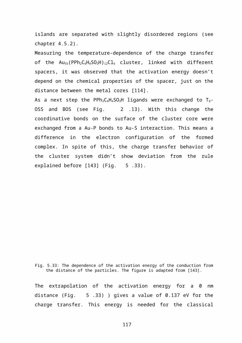
b)
c)
Fig. 6.17: Energy diagram of a cluster system exposed around the left tip (with the cross-linked model): pri-mary state (a), polarized state (b) and the opposite direction polarized states (c). EF denotes the Fermi level.
The cross-linked cluster system can be treated as a cluster polymer, which means that be-
cause of the interaction of the electron-orbitals, the HOMO-LUMO gap is smaller. That
causes an energy difference between the LUMO’s of the exposed and the non-exposed
sides. The conductance in this case happens through the LUMO. If the irradiated side is
negative, (Fig. 6.17 b) then on the border of the non irradiated and irradiated side the elec-
trons have to tunnel “upwards”. If an opposite voltage is applied, this gap is avoided, so the
rectifying effect can be expected. If the interaction of the electron orbitals is not assumed,
the difference in the activation energy in the two directions can lead to the rectification.
Electrons can be added to the system during the exposition with the electron beam, if
somehow electrons are trapped inside the layer. This phenomenon can also be a reason for
the rectifying behavior.
a)
119
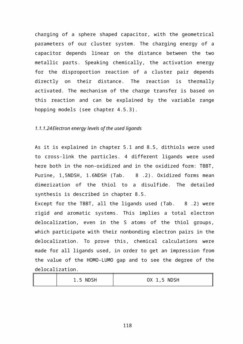
b)
c)
Fig. 6.18: Energy diagram of a cluster system exposed around the left tip (with the trapped charges in the cluster layer model): primary state (a), polarized state (b) and the opposite direction polarized states (c). EF
denotes the Fermi level.
If charges are trapped inside the cluster layer, these electrons occupy a part of the LUMO
states, similar to n doped semiconductors (Fig. 6.18 a). If a voltage is applied to this sys-
tem, with the negative part on the exposed area, the electrons have free way (Fig. 6.18 b).
If the voltage is applied in the opposite direction (Fig. 6.18 c), on the exposed-not exposed
border a gap is formed. The main difference between the expected rectifying behavior of
the cross-linked and this model, that this model assumes the opposite rectifying behavior,
than the one discussed before.
Dispossession of charges can be generated by the exposition to an electron beam, if the
electrons are trapped inside the SiO2 layer. This happens quite easily inside silicon-oxides
and these additional electrons create so-called image charges of opposite charge inside the
120
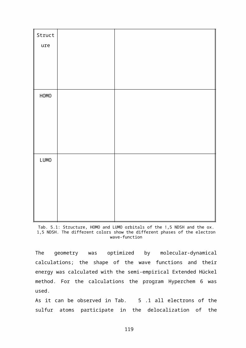
cluster layer. This model predicts a rectifying behavior with the opposite direction as the
above discussed model (Fig. 6.19).
a)
b)
c)
d)
121

Fig. 6.19: Energy diagram of a cluster system exposed around the left tip (with the trapped charges in the SiO2 layer model): primary state (a), polarized state (b) and the opposite direction polarized states (c). EF de-
notes the Fermi level.
The image charges are positive, since the trapped electrons are negative (Fig. 6.19 a). That
means that electrons are missing from the HOMO states, so the conducting electrons have
smaller energy than those in non-exposed parts of the layer (Fig. 6.19 b). The electrons
have thus free way if the exposed area is positive (Fig. 6.19 c), and there is a gap by the ap-
plication of the opposite voltage (Fig. 6.19 d).
If the sample has not the possibility to relax electrically (as it might be in the case of these
substrates) they do not loose they charge after the exposition. So it might happen, that the
top layers of the used platelet remain negatively charged. In this case a charge distribution
may occur, which leads to the formation of negatively charged cluster centers. This small
islands act as a gate for the electron transfer (Fig. 6.20). Speaking in the language of the
energy levels we get the same situation as it was shown on Fig. 6.18, but the cause of the
increase of the energy levels in this case is the higher energy of the negatively charged
clusters in the layer.
Fig. 6.20: Cause of the charge distribution in the case of negatively charged sample.
122
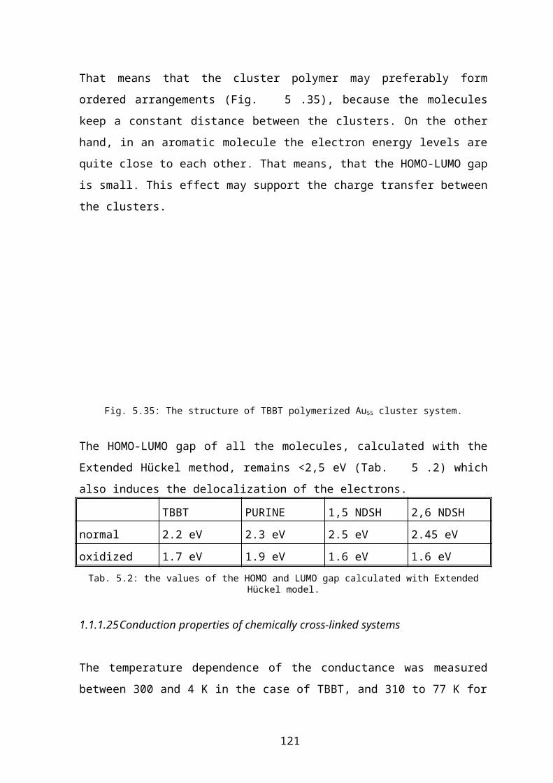
Addition or dispossession of electrons inside the Au55 layer means additional negative or
positive charges in the film. This phenomenon might lead to a rearrangement of the parti-
cles, because the additional charges tend to be delocalized. This delocalization is more ef-
fective, if the entities in a lattice are arranged in a square lattice with a fraction of charge
on every second particle (Fig. 6.21). A very much idealized picture of this situation can be
observed on Fig. 6.21.
exposed area non-exposed area
Fig. 6.21: Rearrangement of the particles in the cluster layer with the delocalization of the charges in the case of the dispossession of the electrons (trapped charges in the SiO2 layer).
The detailed investigation of these three cases shows, that each of them be used to explain
the rectifying behavior, however not in the same direction. In all three cases the change of
the electron configuration might lead to a rearrangement of the particles in the cluster
layer.
6.6.3 Conclusion
Finally the possibility of the above explanations will be discussed in the light of the prop-
erties of the asymmetrical behavior.
The asymmetry in the I-V curve can be discussed in terms of the “cross-linking model”. A
higher energy of bombarding electrons increases the probability of cross-linking reactions
in the sample. An energy threshold can be assumed for the first cross-linking reaction, but
it might be smaller than the smallest energy used for the exposition. Increasing he irradia-
tion energy in terms of the “formation of image charges model” leads also to increasing I-V
asymmetry, since with the increasing energy of the bombarding electrons deeper regions of
the SiO2 layer are available, thus increasing the number of trapped electrons.
123
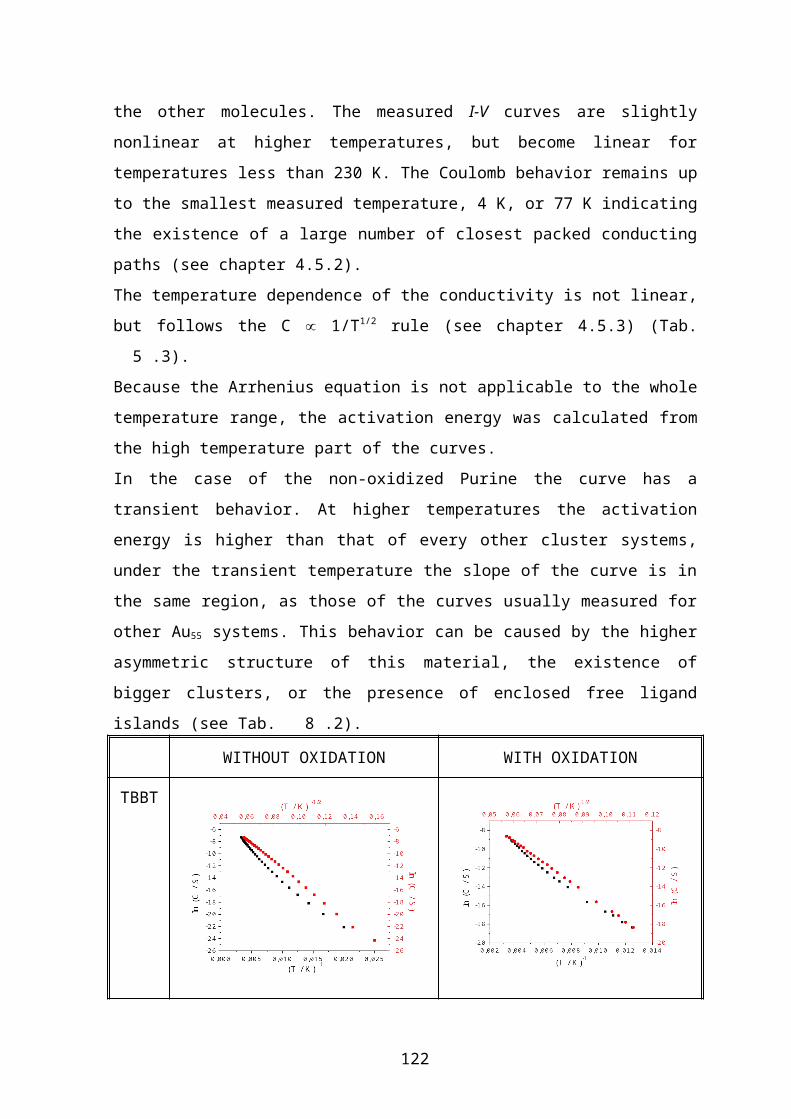
With increasing of the exposition time both the number of the trapped electrons and the
number of the cross-linker bonds can increase.
The dependence of the I-V asymmetry from the SiO2 layer thickness is a strong argument
for the formation of trapped charges, since the cross-linking reaction is not in connection
with the reactions happening in the SiO2 layer.
The decision after the above discussion might be that electrons are trapped inside the SiO2
layer, which inducing image charges of opposite charge in the cluster film. This image
charges might cause dispossession of charges, so forming holes in the layer, or barriers for
the electron movement. This phenomenon might lead to a structural rearrangement in the
cluster layer, accompanied by the delocalization of the charges. This rearrangement and the
change of the electron configuration may lead to the experimentally observed asymmetri-
cal “diode” behavior.
124
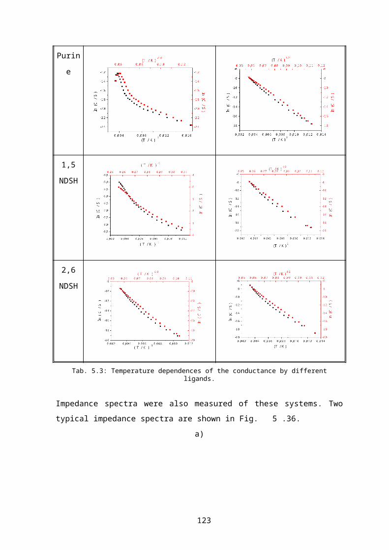
7 Summary
In this study, the electrical properties of Au55 cluster systems were investigated. Two main
topics were addressed:
the difference between the charge transfer mechanism of physically and chemi-
cally cross-linked Au55 systems,
and the conducting properties of dense packed cluster monolayers.
The electrical conductivity measurements were carried out separately for two-, quasi-two,
and three-dimensional arrays of Au55 clusters.
The following problems had to be solved during the work:
- For two-dimensional samples:
A monolayer was prepared with the silanization of a substrate surface, followed
by the deposition of the clusters. These layers consist of large (10 m) dense-
packed islands. These films do not contain any movable ions like H+ or traces of
conducting solutions (see chapter 8.6.2.1 and 5.1.1).
A Langmuir-Blodgett monolayer of Au55(PPh3)12Cl6 has been created on a suit-
able substrate. This monolayer contains traces of conducting solution (water) of
a small concentration. It has been proved that keeping the sample in vacuum,
this solvent can be evaporated, without a significant change in the structure of
the monolayer (see chapter 8.6.1.2 and 5.1.1).
Experimental parameters have been optimized for cross-linking the particles on
the surface (see chapter 8.6.2.1 and 5.1.1).
In a suitable electrode arrangement, the optimal electrode and substrate geome-
try were developed for the electrical conductivity measurements (see chapter
8.6.1.2, 8.7.1.2 and 5.2.1).
- For quasi-two-dimensional samples:
Both chemically and physically cross-linked multilayers of gold nanoparticles
were synthesized. The physically cross-linked layer one spin-coated onto the
substrate (see chapter 8.6.1.1 and 5.1.1), while the chemical layers were pre-
pared with step-by-step self assembly methods (see chapter 8.6.2.2 and 5.1.1).
125
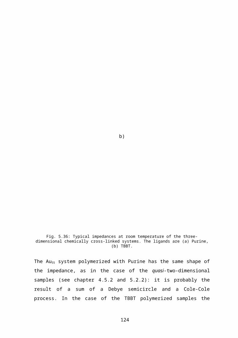
A measurement method has been developed for their electrical characterization,
with a slight modification of the method by U. Simon [114] for three-dimen-
sional samples (see chapter 5.2.2)
- For three-dimensional samples
Conjugated ,-dithiols (1,5 NDSH and 2,6 NDSH) were synthesized and used
as bridging ligands, which form a conjugated electron system inside the cluster
network (see chapter 8.3).
The synthetic parameters were optimized for the cross-linkage reaction of the
Au55 metal cores (see chapter 8.5).
During the work it has been showed that different charge transfer mechanism occurs in
physically and chemically cross-linked systems. The nature of this difference is similar to
the well-known inner-sphere/outer-sphere charge transfer mechanism in aqueous solution
chemistry.
It can also be concluded that the asymmetrical irradiation of the cluster monolayers with an
electron beam leads to an asymmetrical charge transfer behavior. This effect might be
caused by the image charges, which results from trapped charges in the SiO2 layer.
126
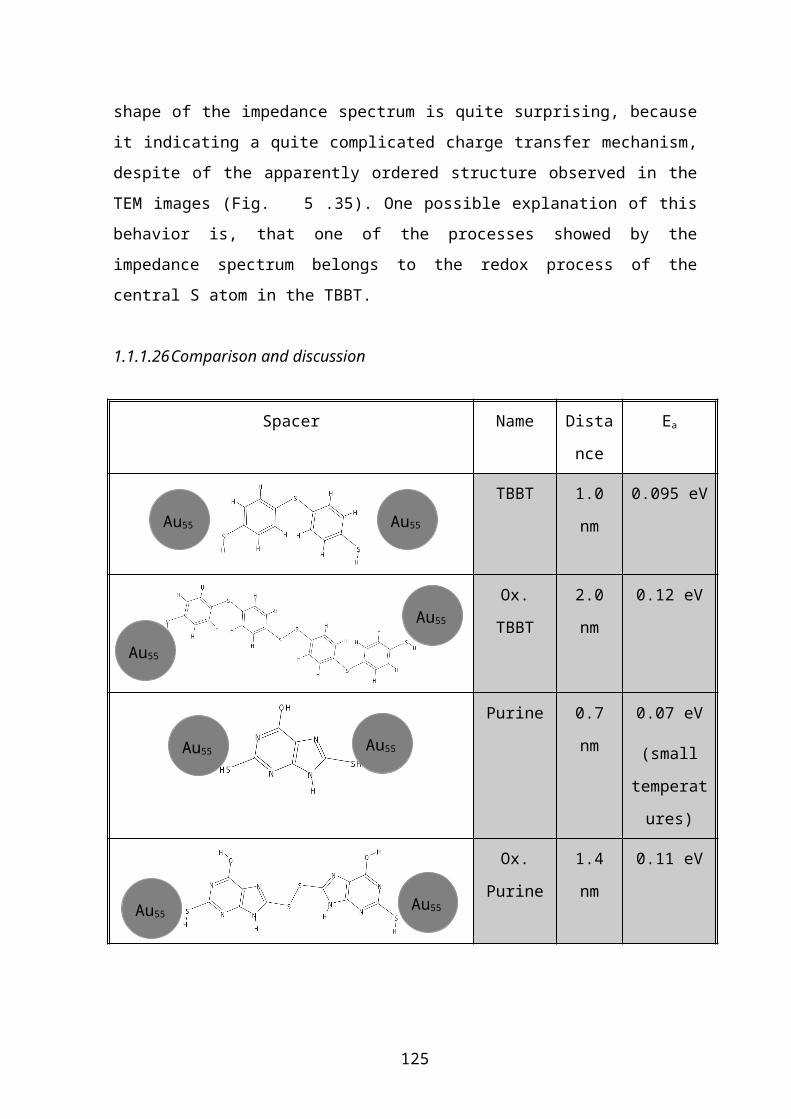
8 Experimental
8.1 Chemicals
NAME FORMULA ABBR. PURIT
Y
DESTI-
NATIO
N
Au55(PPh3)12Cl6
(see fig Fig. 2.9)
Normal Au55 90-95% Synth
[117]
Dichloromethane CH2Cl2 DCM 99.5% Applichem
Ethane-dithiol HS-CH2-CH2-SH EDSH 99% FLUKA
Ethanol CH3-CH2-OH EtOH 99.8% FLUKA
3-mercapto-propyl
trimethoxysilane
(OMe)3Si-(CH2)3-SH TMSPSH 95% ABCR
Toluene C6H5CH3 Toluene 99.5 FLUKA
distilled
1-hydroxy-3,7 dithio-
purine
Purine 98% Avocado
4,4’-thiobis-ben-
zenethiol
TBBT 98% Aldrich
Naphtaline-1,5-disul-
fonic acid sodium salt
1,5NSO3Na 95% Aldrich
Naphtaline-2,6-
disulfonic acid sodium
salt
2,6NSO3Na 95% FLUKA
127

1,5-Dithio-naphtaline 1,5NSH 70% Synth
[146]
2,6-Dithio-naphtaline 2,6NSH 92% Synth
[147]
Sulfolane Sulfolane 99.5% FLUKA
Tetrahydrofurane THF 99.5 FLUKA
distilled
Dimethyl-formamide H(CO)N(Me)2 DMF 99% Acros
Ethyl acetate CH3-CH2-O-(CO)- CH3 EtAc 99.5% FLUKA
Poly-vinyl-pyrrolidone PVP 99.5 FLUKA
3-Chloroprpyl-
dimethylchlorosilane
Cl(Me)2Si-(CH2)3-Cl CDMSPCl 95% ABCR
N,N-dimethyl-O-(3-
chloropropyl-
dimethylsilyl)-
carbamate
(Me2N)O(CO)O(Me)2Si-
(CH2)3-Cl
KDMSPCl 70% Synth
pentane CH3CH2CH2CH2CH3 Pentane 99.7 FLUKA
distilled
Potassium-hydrogen
sulfide
KSH KSH 98% Synth
128
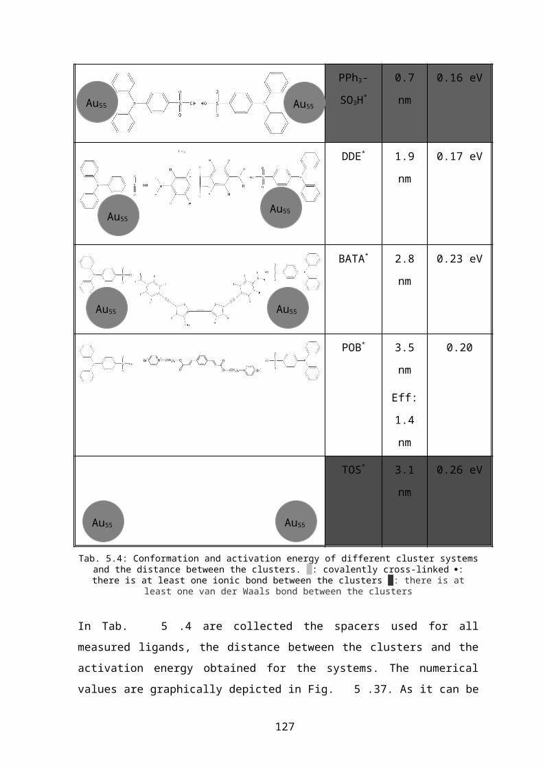
Phosphorus oxychlo-
ride
POCl3 POCl3 99% FLUKA
Mercury-chloride HgCl2 HgCl2 99% Rieder de
Häen
Zinc Zn Zn 98% Roth
Concentrated Sulfuric
acid
cc. H2SO4 cc. H2SO4 98% Baker An-
alysed
Diethyl ether Et2O Et2O 99.5% Roth
Acetonitrile CH3CN MeCN 99.5% FLUKA
Hydrochloric acid HCl HCl 36% FLUKA
Sodium-hydroxide NaOH NaOH 99.9% FLUKA
Tin-chloride SnCl22H2O SnCl2 95% FLUKA
Ammonium chloride NH4Cl NH4Cl 95% FLUKA
Glacial acetic acid CH3-COOH Acetic acid 99-
100%
FLUKA
(Au55Purinex)n Au55(Purine) Synth
(Au55PurineyPuriney)n Ox. Au55(Pu-
rine)
Synth
(Au55TBBTx)n Au55(TBBT) Synth
(Au55TBBTy-TBBTy)n Ox.
Au55(TBBT)
Synth
(Au55(1,5NSH)x)n Au55(1,5NSH) Synth
(Au55(1,5NSH)y(1,5NSH)y)n Ox.
Au55(1,5NSH)
Synth
(Au55(2,6NSH)x)n Au55(2,6NSH) Synth
(Au55(2,6NSH)y(2,6NSH)y)n Ox.
Au55(2,6NSH)
Synth
Tab. 8.1: Names, conformations, abbreviations, purity and source of the chemicals
129
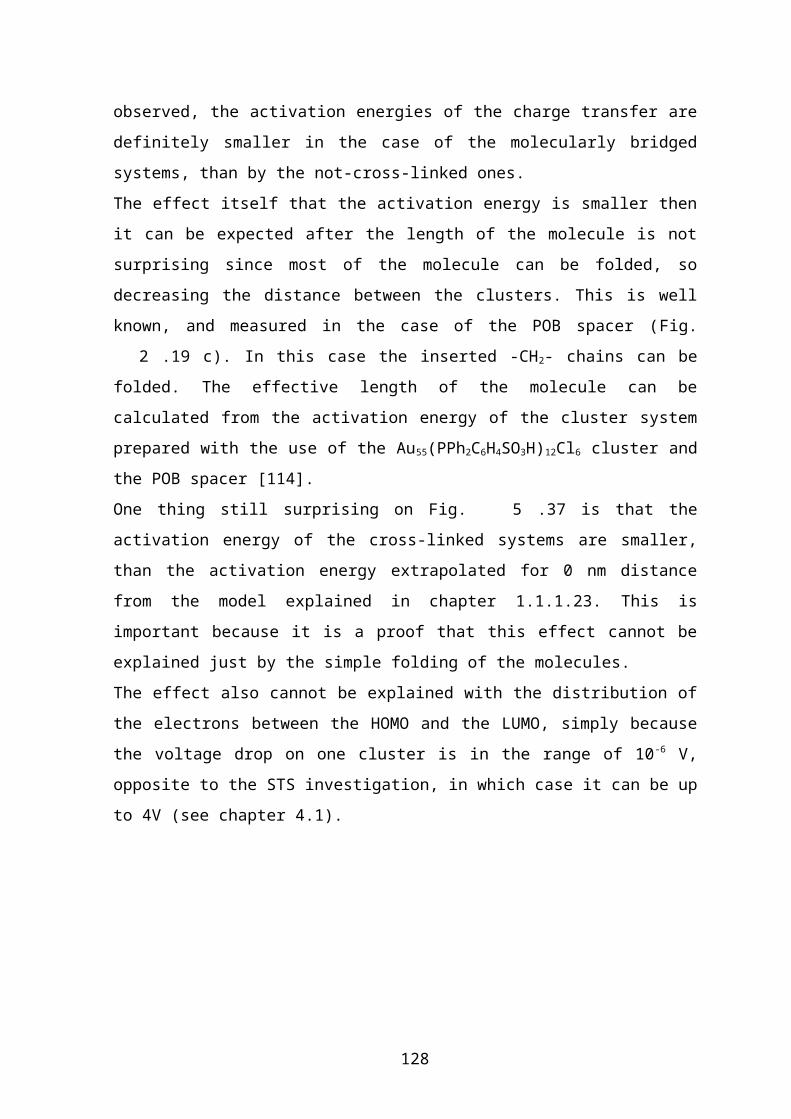
All the solvents and chemicals were used as received, except THF and toluene, which were
distillated on Na/benzophenone and pentane on CaH2. All reactions were carried out in ni-
trogen atmosphere and the solvents were carefully degassed before used.
8.2 Synthesis of the Au55(PPh3)12Cl6 cluster
The Au55(PPh3)12Cl6 cluster was synthesized by the method developed in our working
group in 1981 [116][117]. The main idea of the reaction is that the used gold salt
[Au(PPh3)Cl] is reduced by diborane (see chapter 2.4.1). During the reaction
Au55(PPh3)12Cl6 is formed under certain experimental conditions. For the synthesis first the
apparatus shown on Fig. 8.1 has to be built up.
Fig. 8.1: Apparatus for synthesizing Au55(PPh3)12Cl6 cluster. Figure is adapted from [117].
A 500 ml three-necked, round-bottomed flask [A], containing 20 g of NaBH4 (0.53 mol)
and 100 mL of 1,2-dimethoxyethane, is equipped with a Teflon coated magnetic stirrer, a
dry-ice cooler [E] and a dropping funnel filled with 100 ml BF3-ether [F]. This flask is con-
nected to a second one [M] via a flexible polyethylene tube [L] and a cooled trap [G]. The
second flask, equipped by a magnetic stirrer [C] and a reflux condenser [L] itself con-
D
130
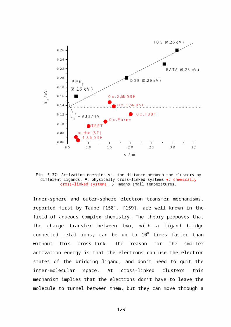
nected to a mercury safety valve [K], is filled with 3,96 g of Au(PPh3)Cl (0.008 mol) and
150 mL of benzene. The trap as well as the dry ice cooler are cooled with a mixture dry-
ice-ethanol. Dropping BF3-ether onto the NaBH4 solution (flask A) induce the formation of
the gas diborane, which via the tube bubble trough the benzene solution heated at 50°C.
The color of the solution changes to brown after few minute and become darker. After 45
min, the production of diborane is stopped and the brown suspension is allowed to cool
back to room temperature. The suspension obtained is then filtered using a sintered funnel.
The precipitate isolated is cleaned with benzene twice and dried two hours under reduce
pressure. The product in then dissolved in CH2Cl 2 and filtered through an Anatop filter to
get rid of the bigger colloids, or recrystalising from a CH2Cl2 solution with the slow addi-
tion of pentane to avoid the presence of smaller particles. The clusters should never remain
in solution more than two or three hours! After two filtration, the clusters are isolated by
evaporation under reduce pressure of the solvent and characterized by TEM.
8.3 Synthesis of the ligands with two terminal –SH groups
Five different ligands with two terminal –SH ligands were used, EDSH, Purine, TBBT,
1,5NDSH and 2,6NDSH (for chemical names see Tab. 8.1). The first three were commer-
cially available. 1,5-Naphtalene-dithiol (1,5NDSH), 2,6-Naphthalene-dithiol (2,6NDSH)
were obtained by reduction of the sodium salts of the corresponding sulfonic acids. Both
syntheses contained two steps: the preparation of sulfonyl chlorides (1) and their reduction
(2).
8.3.1 Synthesis of 1,5-naphtalene-dithiol
1,5-NDSH was synthesized in a two-step synthesis (Eq 3.1).
3.1
First the sulfonyl chloride was prepared with Fujita’s method [145]:
Zn/Hg
33% H2SO4
POCl3
In Sulfolane
131
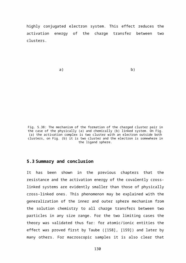
3 g of 1,5NDSO3Na (or 2,6NDSO3Na) (0.009 mol) was added into the mixture of 5.8 mL
acetonitrile (0.11 5.8 mL of sulfolane (0.061 mol) and 4.2 mL of POCl3 (0.045 mol). After
stirring the suspension at 72 C for 3 hours, it was cooled down to 5 C. 50 mL of water
were added into the reaction mixture carefully, then the suspension was stirred another 10
minutes at 10 C. The white precipitate obtained was isolated by filtration and dried in air
overnight.
Reduction of 1,5NDSO2Cl is accomplished with a zinc-amalgam in sulfuric acid [146].
1,25 g HgCl2 (0.0046 mol) was dissolved in 30 mL 0.2M HCl solution and 6,25g Zn (0.095
mol) was added into it. After 10-15 min of stirring , the amalgam was filtered through a
Büchner funnel and washed with water containing a trace of HCl, ethanol and Et2O.
7,5 g of the still wet amalgam was added to the mixture of 45 mL 33% H2SO4 and 1.5 g
sulfonyl chloride (0.0046 mol). The suspension was stirred and refluxed for 6 hours at 110
C. After cooling the obtained suspension was let overnight without stirring at room tem-
perature. The next day, the mixture was filtered and the precipitate extracted with 200 mL
of hot ether. After concentration of the solution, the product was crystallized at low tem-
perature. The white crystals were isolated by filtration and dried under reduce pressure.
(Anal. Calc: C: 62.5; H: 4.16; S: 33.33. Found C: 62; H: 4.18; S: 32.8 %.).
8.3.2 Synthesis of 2,6-naphtalene-dithiol
2,6-NDSH was synthesized in a two-step synthesis. The first step, which resulted in sul-
fonyl chloride, was prepared with Fujita’s method [145], as by the 1,5-NDSH (see chapter
8.3.1).
The reduction of 2,6-NDSO2Cl by SnCl2was realized using Caesar’s method [147].
3.2
For the preparation the following apparatus is needed (Fig. 8.2).
SnCl2
In acetic acid
132

Fig. 8.2: Apparatus for synthesizing 2,6NDSH.
A mixture of 12,5 g (0.066 mol) of stannous chloride dihydrate and 50 mL of glacial acetic
acid (flask [B]) was saturated with anhydrous hydrogen chloride produced by dropping
conc. H2SO4 [A] on NH4Cl [C]. When all the stannous chloride had dissolved, the solution
was heated to 90 C and 1g (0.003 mol) of 2,6NDSO2Cl added quickly with shaking. The
temperature was kept for 30 min and then allowed to cool to room temperature. The sus-
pension was poured into 30 mL of concentrated HCl and filtered. The white precipitate
was extracted with 25 ml of NaOH 5% and the solution was filtrated trough a sintered
glass funnel in 30 mL of HCl concentrated. This procedure was repeated twice and the
solid product dried on air. (elem. anal theoretical C: 62.5%, H: 4.16%, S:33.33%; found C:
61.78%, H: 4.07%, S:32.77%)
8.4 Synthesis of the spacer molecules for the two-dimensional layers
Two different spacer molecule were used: 3-mercapto-propyl trimethoxysilane (TMSPSH)
and N,N-dimethyl-O-(3-chloropropyl-dimethylsilyl)-carbamate (KDMSPCl). The first was
commercially available, but the second had to be synthesized.
AB
C D
EE
F
G
133
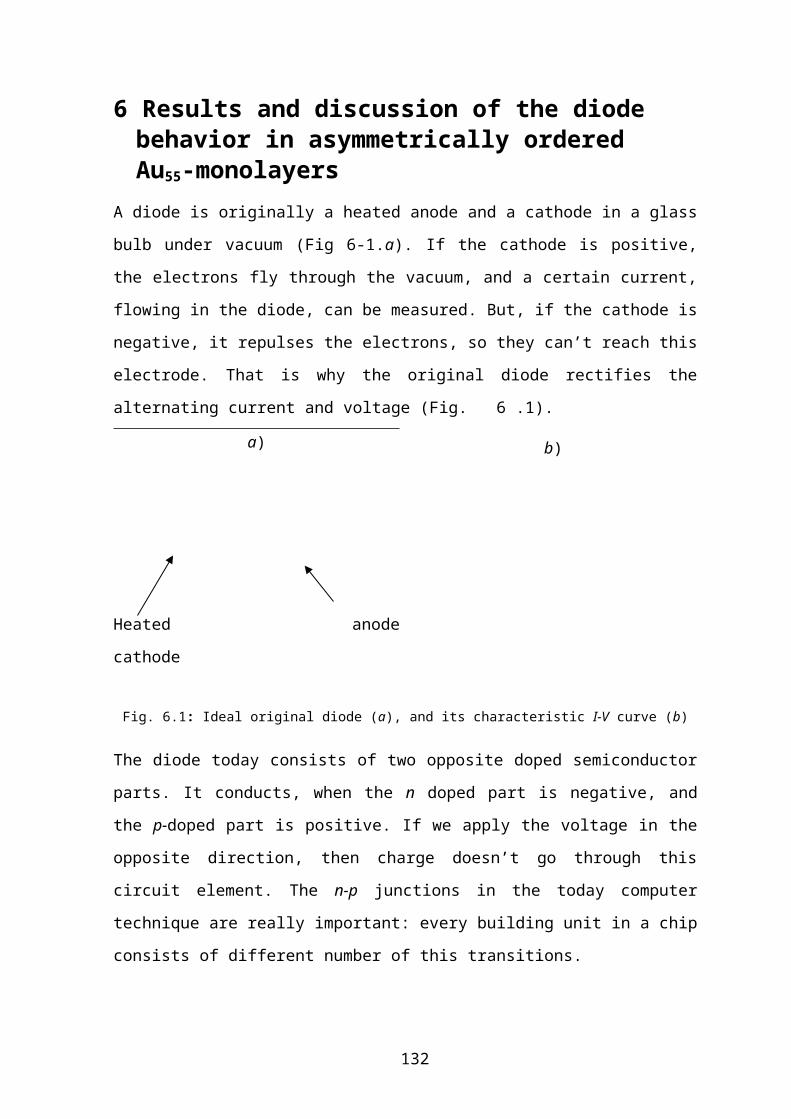
8.4.1 Synthesis of N,N-dimethyl-O-(3-chloropropyl-dimethylsilyl)-carbamate
KDMSPCl was synthesized by Knausz method [156]. All manipulations were carried out
under moisture free conditions. The synthesis involves two steps: first, 2.63 g N,N-
dimethyl-amine (0.116 mol) were treated with carbon dioxide in a dichloromethane solu-
tion. The reaction mixture was cooled with ice. This reaction gives the corresponding
alkylammonium salt of the alkylcarbamic acid:
2 Me2NH + CO2 [Me2NC(O)O]¯Me2NH2+ 3.3
In the second step the carbamate is silylated with a stoichiometric amount (10 g, 0.058
mol) of 3-chloroprpyl-dimethylchlorosilane.
[Me2NC(O)O]¯Me2NH2+ + Cl-SiMe2-C3H6Cl Me2NC(O)O-SiMe2-C3H6Cl
+ Me2NH2+Cl¯
3.3
The silylation of ammonium carbamate salt took 8 hours at room temperature. The N,N-di-
methyl-O-(3-chloropropyl-dimethylsilyl)-carbamate was distilled off in vacuum (B. p. 80-
82 C/1 mmHg). The products were identified by IR and NMR spectroscopy.
8.5 Ligand exchange reactions
Two types of ligand exchange were carried out. The first one was the ligand exchange
trough a solid-liquid interface, this will be presented in chapter 8.6.2. The other, the cross-
linking and precipitation method will be discussed in the following.
A round bottomed flask with nitrogen inlet was charged with 300 ml of dichloromethane,
and 100 mg of Au55(PPh3)12Cl6. The flask was equipped with a dropping funnel which was
filled with 100 ml solutions of the other ligand (Tab. 8.2). The ligands were in 40 times ex-
cess to the cluster. The ligand solution was added dropwise into the flask and mixed vigor-
ously. The ligand exchange reactions were performed under two different conditions: in
the presence and absence of air. The reactions with air turned out to be faster (1-2 hours)
than those without air (3-5 weeks).
The product was purified by washing with CH2Cl2, and the solvent of the ligands. The ele-
mentary analysis results are presented in Tab. 8.2.
134
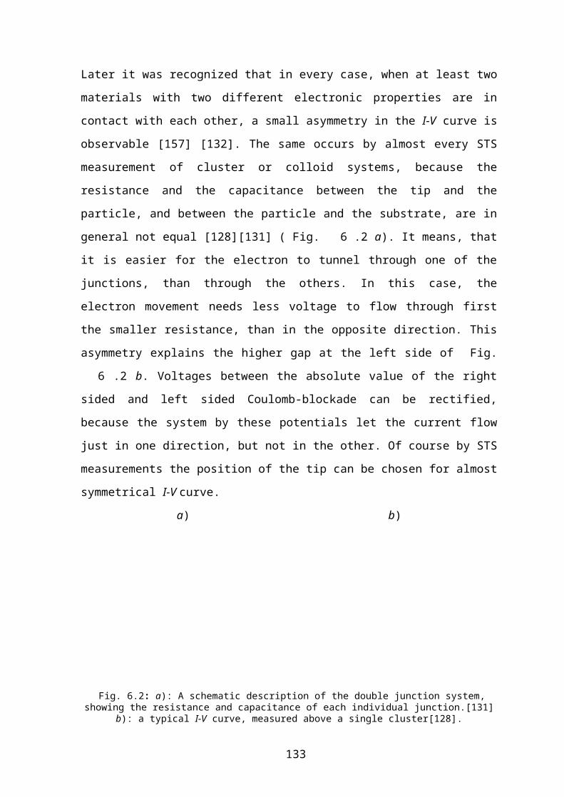
LIGAND AT-MOSPH
ERE
YIELD %
C
M%
H M%
N M%
S M%
AU M%
NEAREST STOI-CHIOMETRY
Sligand
N2 38 13.67 1.34 8.5 6.72 56.9 (Au55(purine)20)n
DMF
Air 66 11.6 0.88 7.18 6.17 63.6 (Au55(purine)16-
-(purine)16)n
DMF
N2 52 19.52 1.32 0 11.2 58.7 (Au55(TBBT)22)n
CH2Cl2
Air 78 16.29 1.1 0 8.18 65,7 (Au55(TBBT)14- -(TBBT)14)nCH2Cl2
N2 59 10.47 0.68 0 3.61 81.21 (Au55(1,5NDSH)8)n
THF
Air 53 18.23 1.14 0 6.76 65.0 (Au55(1,5NDSH)18--(1,5NDSH)18)nTHF
N2 47 19.18 1.65 0 6.21 60.7 (Au55(2,6NDSH)17)n
THF
Air 60 18.32 1.47 0 6.22 64.5 (Au55(2,6NDSH)16--(2,6NDSH)16)nTHF
Tab. 8.2: Solvents of the ligands, and elemental analysis results of the prepared cluster systems.
8.6 Preparations of Au55 layers
8.6.1 Physical layers
8.6.1.1 Dropping and evaporation methods
Quasi-two and quasi-one dimensional samples were prepared with this technique.
135
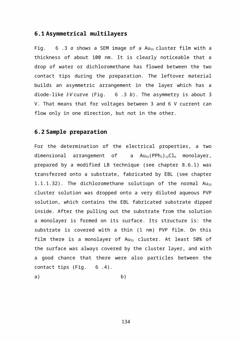
Quasi-two-dimensional samples were fabricated by means of spin-coating technique,
which is discussed in chapter 2.4.5.4 and depicted in Fig. 5.24. 1 mg Au55(PPh3)12Cl6 was
dissolved in 1 mL dichloromethane. This solvent was slowly spin-coated onto a 1x1 cm
quartz plate, with an original roughness of 2 nm. The thickness of the layers (300 and 500
nm) was determinated by AFM.
Quasi-one-dimensional structures were prepared by using a very diluted cluster solution. A
1 mg/100 mL aqueous solution of 15 nm gold colloids was dropped (0.05 mL) onto a
quartz plate. The drying process forms so-called dropping circles arose from the colloids.
The thickness of the ring can be influenced by modification of the concentration of the so-
lution. With this technique microwires were prepared, with cross sections of 1 and 10 m2.
These structures were contacted with conducting silver spots at different distances (50 and
75 m).
8.6.1.2 Modified Langmuir-Blodgett techniques
With this technique Au55(PPh3)12Cl6 layers and chemically cross-linked monolayers were
prepared.
For the preparation of Au55(PPh3)12Cl6 monolayers a dichloromethane solution of normal
Au55 (5.5 mg/10 ml) was dropped onto aqueous PVP solution (1,1 mg/l) containing already
a substrate dipped inside. After evaporation of dichloromethane, the layer was transferred
to the substrate, (cover-glass(8x8 mm), or any other sample), with pulling it out from the
liquid with a speed of about 1cm/3s. With this technique islands of closed Au55 monolayers
could be obtained (Fig. 5.10).
For the preparation of covalently cross-linked Au55 system, 40 l of a normal Au55 solution
(0.55 mg in 10 ml CH2Cl2) was dropped onto a pure water surface, and the solvent was let
evaporate. As a second step a TBBT solution (5.4 mg in 100 ml EtAc) was dropped onto
the water. (the molar ratio of the TBBT/ Au55(PPh3)12Cl6 was 30). After waiting for 30 sec-
onds the sample was pulled out with a speed of 0.8 cm/s (see Fig. 5.11).
136
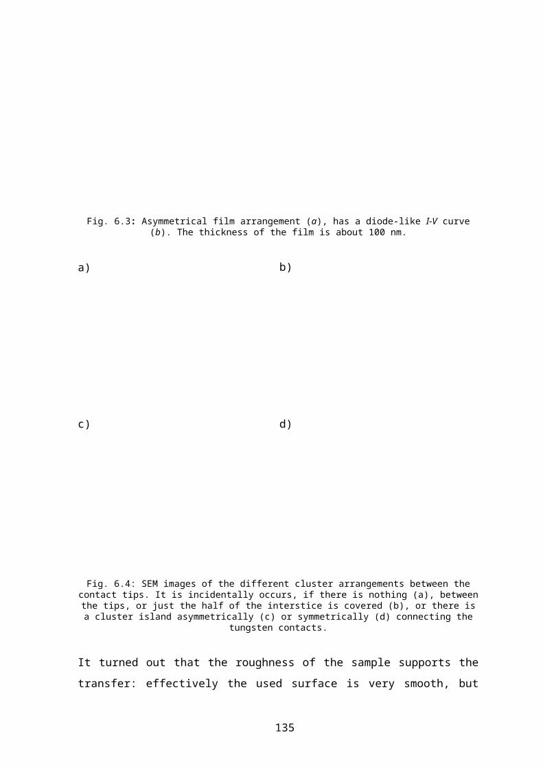
8.6.2 Chemical layers
Chemical methods for the layer preparation start with the modification of the substrate sur-
face, followed by the chemisorption of the clusters. In this work both mono- and multilay-
ers were prepared using this technique.
8.6.2.1 Preparation of a monolayer
The experiment was divided in 4 steps: a glass substrate was first dipped into a 0.2 M HCl
solution (30 min) and then into 3-chloropropyl-dimethylsilan-carbamate for 2 hours under
N2 atmosphere. After washing the sample carefully with pentane to remove the excess of
the silane, it was heated for 30 minutes to 120°C into a drying box. The thickness of the
layer measured by AFM was smaller than 0.5 nm. Thereafter, the sample was successively
dipped in an ethanol solution of KSH for 30 min, washed with ethanol, to remove the ex-
cess of the KSH, dipped into a Au55(PPh3)12Cl6 dichloromethane solution for 30 min, and
finally washed with CH2Cl2. With this method a monolayer was obtained with relative big
closed islands of clusters (up to 10 m). To cross-link the deposited particles, the sample
was dipped into a dithiol solution for 30 min and washed with the solvent selected to solu-
bilize the linker used (the solvents list is presented in Tab. 8.2).
8.6.2.2 Preparation of a multilayer
For these experiments 3-chloropropyl-trimethoxisilane was used [148]. The glass sample
was first dipped into HCl solution to increase the concentration of the surface –OH groups.
Then, the substrate was refluxed for 24 hours in a toluene solution of TMSPSH (5 mL TM-
SPSH into 100 ml toluene). The 16 nm thick silane layer obtained (AFM measurement)
was washed with toluene, and thereafter dipped into a cluster solution (0.1 g/mL). To pre-
pare multilayers, this substrate was dipped into an ethanol solution of ethane dithiol (the
volume ratio was 80:1), and back to the cluster solution. These last two steps were repeated
several times. The as-prepared samples were connected with conducting silver spots with a
diameter of approximately 1 mm.
137
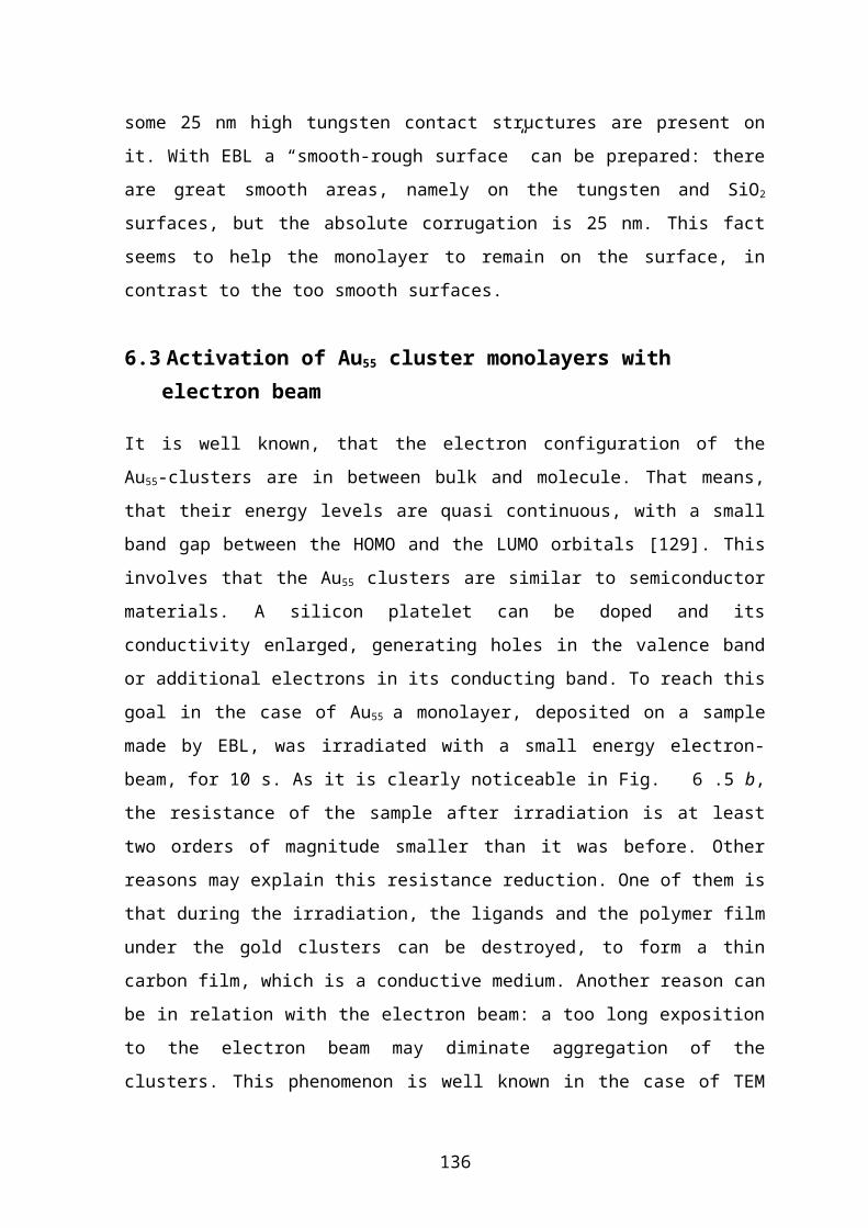
8.7 Instrumental
8.7.1 Preparations
8.7.1.1 Langmuir-Blodgett instruments
Two different modified Langmuir-Blodgett (LB) instruments were used. The first and easi-
est one was prepared from an old microscope stand. The table was fixed in a certain posi-
tion, and tweezers were attached to the movable focus adjuster screw, so that the angle and
its position could be changed. A Petri cup was placed onto the microscope table. The sub-
strate was fixed between the tweezers and moved inside the cup. The used liquid was filled
into the Petri cup so that the substrate was fully dipped into it and the other liquid was
dropped on top of it. After evaporation of the second solvent, the sample was pulled out
slowly.
The other instrument was a self-built modified LB-instrument. It consisted of a motor
(Newport 850 F) and a Controller (Newport Motion Control MM4000), regulated by a PC.
The substrate was fixed on the motor-arm, to draw it into and to pull it out of the solvent.
With changing the position of the motor, the angle of immersion can be controlled between
15 and 90. Another motor (Actuator 850 F) moved Teflon barrier, which compressed the
surface of the liquid in the trough. The trough was made of Teflon. Unfortunately, there
was no instrument for measuring the surface pressure in this case.
The sample was fixed at the motor-arm and moved into the liquid that filling the trough.
Another solution was dropped onto the surface, and let the solvent evaporate. The barrier
compressed the surface and at least the sample was pulled out from the trough.
8.7.1.2 Sample preparation for the two-dimensional measurements
The samples for the two-dimensional measurements were prepared by Prof. Dr. C. Rade-
haus and M. Schumann in the Technical University of Chemnitz by electron beam lithogra-
phy. A Si wafer was oxidized on its surface during the formation of an 80 nm SiO2 layer. It
was covered with a tungsten film, then with an electron beam sensitive lack. The as-pre-
138
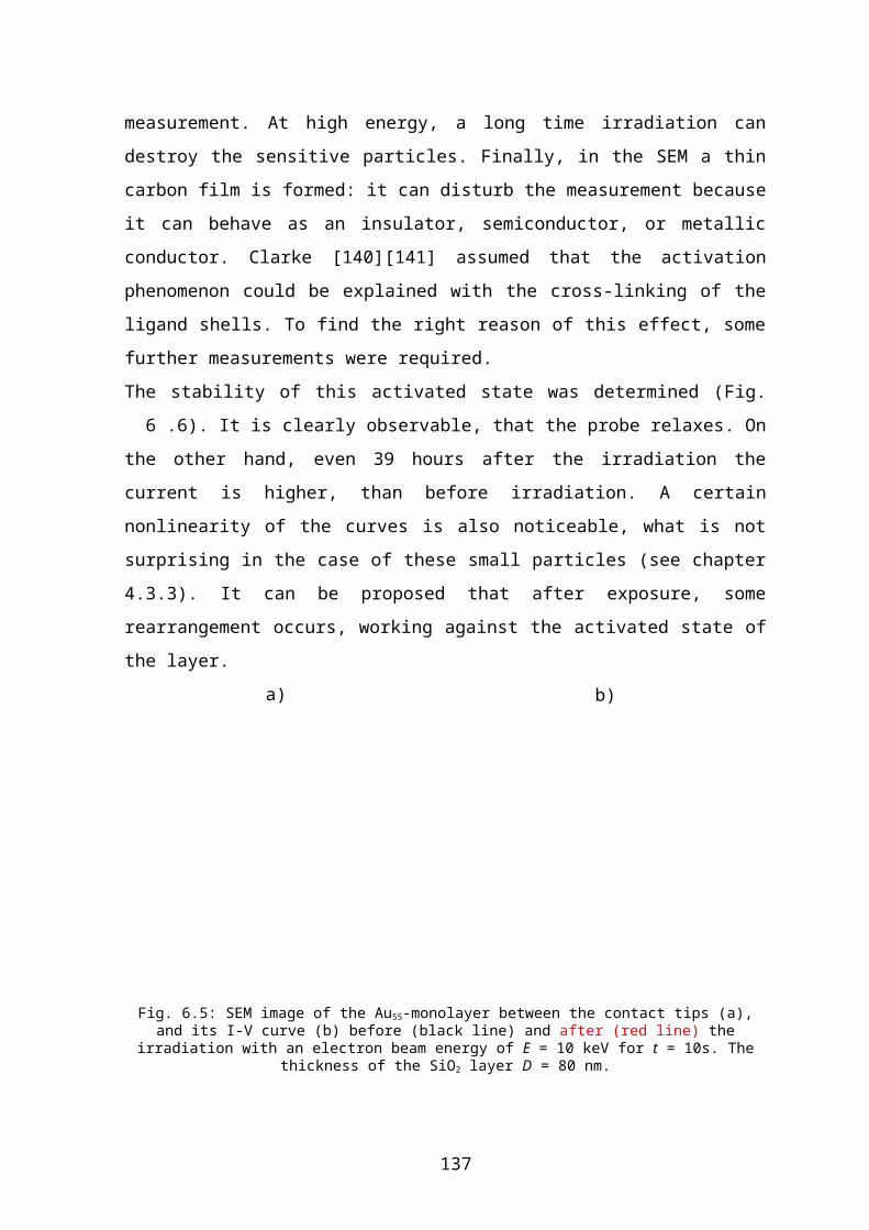
pared sample was exposed to an electron beam. As a result, of this the exposed part of the
lack will be water soluble, so it can be easily removed without disturbing the other part of
the substrate. The tungsten on the lack-free parts is dissolved by an acid. As a last step the
lack is removed with some organic solvent (Fig. 8.3).
Fig. 8.3: Sample preparation with electron beam lithography. A Si wafer is oxidized on its surface, and cow-ered with a Tungsten film, and an electron beam sensitive lack. After the exposure to an electron beam, the
exposed part of the lack will be water soluble, so it can be washed. The tungsten on the wished parts are dis-solved and at least the lack is removed.
The substrates obtained with this technique is shown in Fig. 8.4. The relative big squares
are the contact pads. For the measurements they will be contacted with sharp tips. The long
wires are contacts leading to tips on the surface. The two wires coming from left and right
are the source and the drain, with a distance of 20 to 100 nm, the third one is a little farther
used as the gate electrode. Many images of the contact structures can be found in chapter 6.
Fig. 8.4: A light microscopic image of the contact pads prepared by electron beam lithography.
Another type of electron beam lithographically prepared samples are the comb structures.
This means that the two electrodes are like two combs opposite to each other (Fig. 8.5.)
139
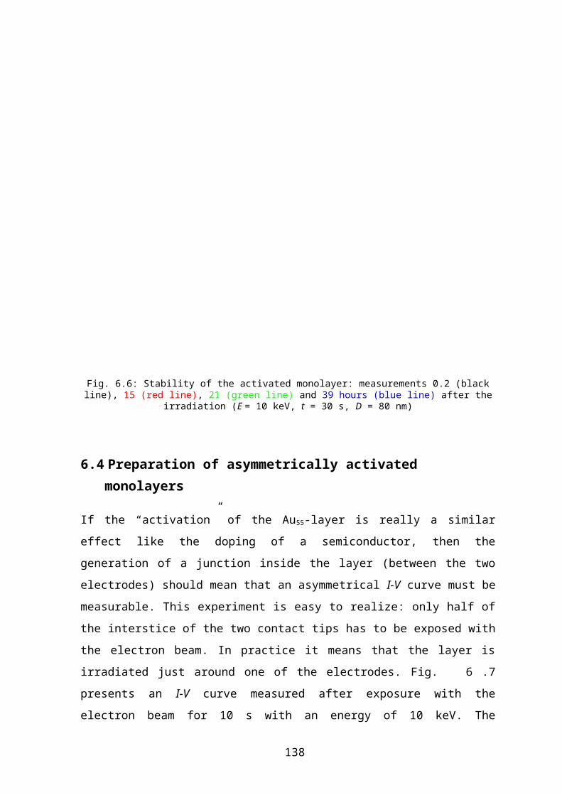
Fig. 8.5: SEM image of the comb structures prepared by electron beam lithography. The right picture is a zoom of the left one.
The sizes of the combs are 1x6 (A), 1x10 (B) and 3x10 (C) m. The distances of the elec-
trodes vary between 100-200 nm, the breadths of them are between 100 and 200 nm.
8.7.2 Preparation of the three-dimensional samples
For the electrical measurements the samples were pressed into pellets with a pressure of
4107 Pa for 5 min, and then let relax for another 5 min. The shape of the pellets was
cylindricwith approximately 0.2 mm of thickness, and 0.5 cm diameter. They were con-
nected from the bottom and the top with conducting silver spots
8.7.3 Equipments
The characterisation of the samples were carried out by a Nanoscope II Atomic Force Mi-
croscope.
TEM measurements was performed using a Philips CM 200 FEG transmission electron mi-
croscope at 200 kV.
The activation energy measurements was performed on a Keithley 2400 instrument.
The measurements on the electron beam lithography fabricated samples was carried out by
a Keithley 236 SMU.
The impedance measurements was performed on a Zahner IM6e instrument with a SIM
software.
140

9 Literatur
[1] G. Schmid, Custers and Colloids: from theory to applications, WCH Publishers, New York, (1994)
[2] J. Bardeen and W. H. Brattain, Phys. Rev. 74, 230 (1948)
[3] B. E. Deal, Interface 6, 18 (1997)
[4] D. L. Feldheim and C. D. Keating, Chem. Soc. Rev. 37 1, (1998)
[5] A. O. Orlov, I. Amlani, G. H. Berstein, C. S. Lent, and G. L. Snider, Science, 277, 928 (1997)
[6] J.R. Heath, P.J. Kuekes, G. Snider, R.S. Williams, Science, 280, 1716 (1998)
[7] C. J. Gorter, Physica 17 777 (1951)
[8] I. Giaver and H. R. Zeller, Phys. Rev. 20, 1504 (1968)
[9] I. Giaver and H. R. Zeller, Phys. Rev. Lett. 181, 789 (1969)
[10] P. Braunstein, L. A. Oro, P. R. Raithby, Metal clusters in chemistry Wiley-WCH, New York (1999)
[11] F. E. Kruis, H. Fissan, A. Peled, J. Aerosol. Sci. 29, 511, (1998)
[12] R. P. Andres, T. Bein, M. Dorogi, S. Feng J. I. Henderson, C. P. Kubiak, W. Mahoney, R. D. Osifchin, R. Reifenberger, Science, 272, 1323 (1996)
[13] M. Dorogi, J. Gomez, R. D. Osifchin, R. P. Andres, R. Reifenberger, Phys. Rev. B, 52, 9071, (1995)
[14] B. Wang, X. Xiao, P. Sheng, J. Vac. Sci. Technol. B., 18, 2351 (2000)
[15] C. P. Vinod, G. U. Kulkani, C. N. R. Rao, Chem. Phys. Lett. 289, 329, (1998)
[16] M.N. Vargaftik, V.P. Zargorodnikov, I.P. Stolarov, I.I. Moiseev, V.A. Likholobov, D.I. Kochubey, A.L. Chuvilin, V.I. Zaikosvsky,_ . K.I. Zamaraev, G.I. Timofeeva, J. Chem. Soc., Chem. Commun. 937–939 (1985)
[17] H. Hirai, J. Macromol. Sci. – Chem. A13, 633, (1979)
[18] M. Faraday, Phil. Trans. Roy. Soc. 147, 145 (1857)
141
[19] H. B0nnemann, W. Brijoux, R. Brinkmann, E. Dinjous, R. Fretzen, T. Joussen, B. Korall, J. Mol. Catal. 74, 323, (1992)
[20] J. Turkevitch, P. C. Stevenson, J. Hillier, Disc. Faraday Soc. 11 55 (1951)
[21] J. Turkevitch, R. S. J. Miner, I. Okura, S. Namba, Proc Swedish. Symp. Catal. 111 (1981)
[22] D. N. Furlong, A. Launikonis, W. H. F. Sasse, J. V. Saunders, J. Chem. Soc. Faraday Trans. 80. 571 (1984)
[23] A. Harriman, G. R. Millward, P. Neta, M. C. Richoux, J. M. Thomas, J. Phys. Chem. 92, 1286, (1988)
[24] J. Turkevitch, G. Kim, Science 169, 873, (1970)
[25] M. Brust, M. Walker, D. Bethell, D. J. Schiffrin, R. Whymann, Chem. Commun. 801 (1994)
[26] M. Brust, D. Bethel, D. J. Schiffrin, C. J. Kiely, Adv. Mater. 7. 795, (1995)
[27] A. C. Templrton, S. Chen, S. M. Gross, R. W. Murray, Langmuir, 15 66 (1999)
[28] P. H. Hess, P. H. Parker, J. Appl. Polym. Sci. 10, 1915, (1966)
[29] J. R. Thomas, J. Appl. Phys. 37, 2914 (1966)
[30] B. G. Esrshov, e. Janata, M. Michaelis, A. Henglein, J. Phys. Chem. 95, 8996, (1991)
[31] G. B. Khomutov, A. Yu Obydenov, S. A. Yakovenko, E. S. Soldatov, A. S. Trifonov, V. V. Khanin, S. P. Gubin, Mat. Sci. Eng, C8-9, 309, (1999)
[32] Suslick, K. S.; Choe, S.-B.; Cichowlas, A. A.; Grinstaff, M. W. Nature, 353, 414 (1991)
[33] Grinstaff, M. W.; Cichowlas, A. A.; Choe, S.-B.; Suslick, K. S. Ultrasonics, 30, 168. (1992)
[34] F. Dassenoy, K. Philippot, T. O. Ely,C. Amiens, P. Lecante,E. Snoeck, A. Mosset, M. J. Casanove, B. Chaudret, New J. Chem. 703 (1998)
[35] A. Rodriguez, C. Amiens, B. Chaudret, M. J. Casanove, P. Lecante J. S. Bradley, Chem. Mater., 8, 1978 (1996)
[36] S. Roginsky, A. Schalnikoff, Kolloid Z. 43, 67, (1927)
142

[37] J. S. Bradley, E. W. Hill, M. E. Leonowitz, H. Witzke, J. Mol. Catal. 41, 59 (1987)
[38] M. T. Reetz, W. Helbig, S. A. Quaiser, in A. Fürstner (ED.), Active metals: Prepara-tion, Characterisation, Application, VCH, New York (1996)
[39] N. Toshima, T. Takahashi, Bull. Chem. Soc. Japan, 65, 400 (1992)
[40] P. A. Jacobs, N. I. Jaeger, P. Jiru, G. Schulzeklo (eds) Metal microstructures in zeo-lites. Elsevier, Amsterdam (1982)
[41] R. Pelster, U. Simon, Colloid Polym. Sci. 277, 2 (1999)
[42] R. S. Bowles, J. J. Kolstad, J. M. Calo, R. P. Andres, Surf. Sci. 106, 117, (1981)
[43] A. N. Patil, D. Z. Paithankar, N. Otsuka, R. P. Andres, Z. Phys, D26, 135 (1993)
[44] R. P. Andres, J. D. Bielefeld, J. I. Henderson, D. B. Janes, V. R. Kolagunts, C. P. Kubiak, W. J. Mahoney, R. G. Osifchin, Science, 273, 1690 (1996)
[45] T. T. Yau, P. Mulvaney, W. Xu, G. M. Spinks, Phys. Rev. B, 57, R124 (1998)
[46] K. V. Sarathy, G. Raina, R, T. Yadav, G. U. Kulkarni, C. N. R. Rao, J. Phys. Chem B, 101, 9876, (1997)
[47] S. J. Green, J. J. Pietron, J. J. Stokes, M. J. Hostetler, H. Vu, W. P. Wuelfing, R. W. Murray, Langmuir, 14, 5612, (1998)
[48] K. S. Mayya, V. Patil, M. Sastry, Bull. Chem. Soc. Jpn. 73, 1757, (2000)
[49] M. Rolandi, K. Scott, E. G. Wilson, F. C. Meldrum, J. Appl. Phys. 89, 1588, (2001)
[50] M. Brust, D. Bethell, D. J. Schiffrin, C. J. Kiely Adv. Mater. 7, 795,(1995)
[51] S. Chen, J. Phys. Chem B, 104, 663, (2000)
[52] L. Han, M. M. Maye, F. L. Leibowitz, N. K. Ly, C. J. Zhong, J. Mater. Chem. 11, 1258 (2001)
[53] F. L. Leibowitz, W. X. Zheng, M. M. Maye, C. J. Zhong, Anal. Chem. 71, 5076 (1999)
[54] J. R. MacDonald, Impedance Spectroscopy, Wiley, New York, (1987)
[55] D. L. Klein, P. L. McEuen, J. E. Bowen Katari, R. Roth, A. P. Alivisatos, Appl. Phys. Lett. 68, 2574, (1996)
143
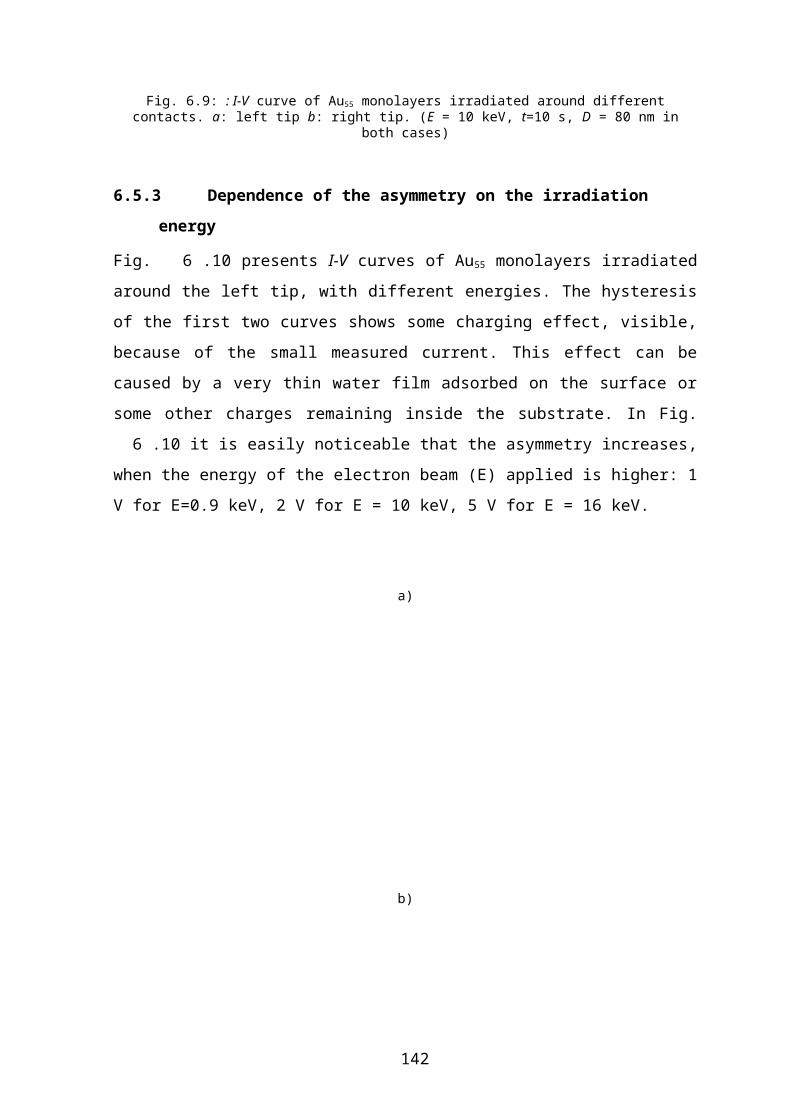
[56] M. Brust, D. Bethell, C. J. Kiely, D. J. Schiffrin, Langmuir, 14, 5425, (1998)
[57] T. Sato, H. Ahmed, D. Brown, B. F. G. Johnson, J. Appl. Phys. 82, 696, (1996)
[58] T. Vossmeyer, E. DeIonno, J. R. Heath, Angew.Chem. 109, 1123, (1997)
[59] S. Chen, R. W. Murray, J. Phys. Chem. B, 103, 9996, (1999)
[60] S. Chen, R. W. Murray, Langmuir, 15, 682, (1999)
[61] S. Chen, Adv. Matter. 12, 186, (2000)
[62] S. Chen, Langmuir 17 2878, (2001)
[63] M. J. Hostetler, A. C. Templeton, R. W. Murray, Langmuir, 15, 3782 (1999)
[64] L. C. Brousseau, S. M. Marinakos, J. P. Novak, D. L. Feldheim, Mater. Res. Bull. 129 (1998)
[65] T.-A. Hanaoka, A. Heilmann, M. Kröll, H.-P. Kormann, T. Sawitowski, G. Schmid, P. Jutzi, A. Klipp, U. Kreibig, R. Neuendorf, Appl. Organomet. Chem. 12, 367, (1998)
[66] S. T. Yau, P. Mulvanez, W. Xu, G. M. Spinks, Phys. Rew. B, 57, R15 124, (1998)
[67] M. Y. Han, L. Zhou, C. H. Quek, S. F. Y. Li, W. Huang, Chem. Phys. Lett. 287, 47, (1998)
[68] M. Dorogi, J. Gomez, R. Oschifchin, R. P. Andres, R. Reifenberger, Phys. Rew. B, 52, 9071 (1995)
[69] R. P. Andres, T. Bein, M. Dorogi, S. Feng, J. I. Henderson, C. P. Kubiak, W. Mahoney, R. Oschifchin, , R. Reifenberger, Science, 272, 1323 (1996)
[70] T. Junno, M. H. Magnusson, S. B. Carlsson, K. Deppert , J. O. Malm, L. Montelius, L. Samuelson Microelectronic Eng. 47 179 (1999)
[71] S. H. M. Persson, L. Olofsson L. Gunnarsson, Appl. Phys. Lett. 74, 2546 (1999)
[72] A. Bezryadin, C. Dekker, G. Schmid, Appl. Phys. Lett. 71 1273 (1997)
[73] T. Junno, S. B. Carlsson , H. Q. Xu, L. Montelius, L. Samuelson, Appl. Pys. Lett. 72 548 (1998)
144

[74] S. W. Chung, G. Markovich, J. R. Heath, J. Phys. Chem. B, 102, 6685, (1998) S. M. Marinakos, L. C. Brousseau, A. Jones, D. L. Feldheim, Chem Mater. 10 1214 (1998)
[75] M. Gleiche, Li F. Chi, H. Fuchs, Nature, 403 173, (2000)
[76] L. C. Brousseau, S. M. Marinakos, J. P. Novak, D. L. Feldheim, Mater. Res. Bull. Suppl. S 129, (1998)
[77] C. A. Berven, M. N. Wybourne, L. Clarke, J. E. Hutchison, L. O. Brown, J. L. Mooster, M. E. Schmidt, Supelattices and Microstructures, 27 489 (2000)
[78] J Richter, M Mertig, W Pompe, I. Mönch, H. K. Schackert, Appl. Phys. Lett. 78, 536 (2001)
[79] C. Gutierrez-Wing, P. Santiago, J. A. Ascencio, A. Camacho, M. Jose-Yacaman, Appl. Phys. A, 71 237 (2000)
[80] J. Zheng, Z. Zhu, H. Chen, Z. Liu, Langmuir, 16, 4409, (2000)
[81] L. Motte, E. Lacaze, M. Maillard, M. P. Pileni, Langmuir, 16, 3803, (2000)
[82] L. Motte, F. Billoudet, E. Lacaze, J. Douin, M. P. Pileni J. Phys. Chem. B, 101, 138 (1997)
[83] M. J. Hostetler, J. E. Wingate, C. J. Zhong, J. E. Harris, R. W. Vachet, M. R. Clark, J. D. Londono, S. J. Green, J. J. Stokes, G. D. Wignall, G. L. Glish, M. D. Porter, N. D. Evans, R. W. Murray, Langmuir, 14, 17, (1998)
[84] J. Fink, C. J. Kiely, D. Bethell, D. J. Schiffrin, Chem. Mater. 10, 922 (1998)
[85] J. R. Heath, C. M. Knobler, D. V. Leff, J. Phys. Chem. B, 101, 189 (1997)
[86] C. P. Collier, R. J. Saykally, J. J. Shiang, S. E. Henrichs, J. R. Heath, Science, 277, 1978 (1997)
[87] J. P. Bourgoin, C. Kergueris, E. Lefevre, S. Palacin, Thin Solid Films, 329 515 (1998)
[88] K. S. Mayya, M. Sastry, Langmuir, 15, 1902, (1999)
[89] T. Zhu, X. Zhang, J. Wang, X. Fu, Z. Liu, Thin Solid Films, 327, 595, (1998)
[90] D. Bethell, M. Brust, D. J. Schiffrin, C. Kiely, J. Electroanal. Chem. 409, 137, (1996)
145

[91] K. C. Grabar, P. C. Smith, M. D. Musick, J. A. Davis, D. G. Walter, M. A. Jackson, A. P. Guthrie, M. J. Natan, J. Am. Chem. Soc. 118, 1148, (1996)
[92] T. Sato, D. Brown, B. F. G. Johnson, Chem. Commun., 1007 (1997)
[93] D. M. Schaefer, R. Reifenberger, A. Patil, R. P. Andres, Appl. Phys. Lett. 66, 1012, (1995)
[94] J. P. Spatz, S. Mössmer, C. Hartmann, M. Möller, T. Herzog, M. Krieger, H.-G. Boyen, P. B. Kabius, Langmuir, 16, 407 (2000)
[95] D. L. Feldheim, K. C. Grabar, M. J. Natan, T. E. Malluk, J. Am. Chem. Soc. 118, 7640, (1996)
[96] Y. J. Liu, Y. X. Wang, R. O. Claus, Chem. Phys. Lett. 298, 315 (1998)
[97] E. Hao, T. Lian, Chem. Mater. 12, 3392 (2000)
[98] A. N. Shipway, M. Lahav, I. Willner, Adv. Mater. 12, 993 (2000)
[99] F. Auer, M. Scotti, A. Ulman, R. Jordan, B. Sellergren, J. Garno, G.-Y. Liu, Langmuir, 16, 7554 (2000)
[100] A. Kumar, A. B. Mandale, M. Sastry, Langmuir, 16, 6921, (2000)
[101] M. D. Musick, C. D. Keating, L. A. Lyon, S. L. Botsko, D. J. Pena, W. D. Holliway, T. M. McEvoy, J. N. Richardson, M. J. Natan, Chem. Mater. 12, 2869, (2000)
[102] K. V. Sarathy, P. J. Thomas, g. u. Kulkarni, C. N. R. Rao, J. Phys. Chem. B, 103, 399, (1999)
[103] D. B. Janes, M. Batistuta, S. Datta, M. R. Melloch, R. P. Andres, J. Liu, N. P. Chen, T. Lee, R. Reifenberger, E. H. Chen, J. M. Woodall, Superlattices and Microstruc-tures, 27, 555, (2000)
[104] W. P. McConnell, J. P. Novak, L. C. Brousseau, R. R. Fuierer, R. C. Tenent, D. L. Feldheim, J. Phys. Chem. B, 104, 8925 (2000)
[105] P. J. Thomas, G. U. Kulkarni, C. N. R. Rao, Chem. Phys. Lett. 321 163–168 (2000)
[106] T. Sato, H. Ahmed, Appl. Phys. Lett. 70 2759 (1997)
[107] A. N. Korotkov, Molecular Electronics, (1996)
[108] U. Simon, V. Gasparian, Phys. Stat. Sol. B, 205, 223 (1998)
146
[109] R. P. Andres, S. Datta, S. Dorogi, J. Gomez, J. I. Henderson, D. B. Janes, V. R. Ko-lagunta, C. P. Kubiak, W. Mahoney, R. F. Osifchin, R. Reifenberger, M. P. Samanta, W. Tian, J. Vac. Sci. Technol. A 14, 1178, (1996)
[110] H. Perez, R. M. Lisboa, de Sousa, J-P. Pradeau, P-A. Albouy, Chem. Mater., 13, 1512 2001)
[111] Y. J. Liu , Y. W. Wang , R. O. Claus, Chem. Phys Lett. 298 315 (1998)
[112] R. H. Terril, T. A. Postlethwaite, C. Chen, C.-D. Poon, A. Terzis, A. Chen, J. E. Hutchinson, M. R. Clark, G. Wignall, J. D. Londono, R. Superfine, M. Falvo, C. S. Johnson, E. T. Samulski, R. W. Murray, J. Am. Chem. Soc. 117, 12537 (1995)
[113] W. P. Wuelfing, S. J. Green, J. J. Pietron, D. E. Cliffel, R. W. Murray, J. Am. Chem. Soc. 122 11465 (2000)
[114] U. Simon, Habilitationsschrift Universität Essen (1998)
[115] N. Sandhyarani, M. R. Resmi, R. Unnikrishnan, K. Vidyasagar, Shuguang Ma, M. P. Antony, G. Panneer Selvam, V. Visalakshi, N. Chandrakumar,Kannaiyan Pandian, Yu-Tai Tao, T. Pradeep, Chem. Mater, 12, 104.(2000)
[116] G. Schmid, R. Pfeil, R. Boese, F. Bandermann, S. Meyer, G. H. M. Calis, J. A. van der Velden, Chem. Ber. 114, 3634, (1981)
[117] G. Schmid, Inorg. Synth. 7, 214, (1990)
[118] J. D. Aiken, R. G. Finke, J. Mol. Cat. A, 145 1 (1999)
[119] F. M. Mulder, R. C. Thiel, L. J. de Jongh, P. C. M. Gubbens, Nanostruct. Mater. 7, 269 (1996)
[120] G. Schmid, Tetrahedron, 7, 2321 (1988)
[121] G. Schmid, R. Pugin, J.-O. Malm, J.-O. Bovin, Eur. J. Inorg. Chem. 813 (1998)
[122] G. Schmid, R. Pugin, W. Meyer-Zaika U. Simon, Eur. J. Inorg. Chem. 2051 (1999)
[123] R. Flesch, Dissertation, Universität Essen, (1997)
[124] G. Schmid, J. Chem.Soc., Dalton Trans. 1077, (1998)
[125] S. Peschel, Dissertation, Universität Essen, (1997)
147
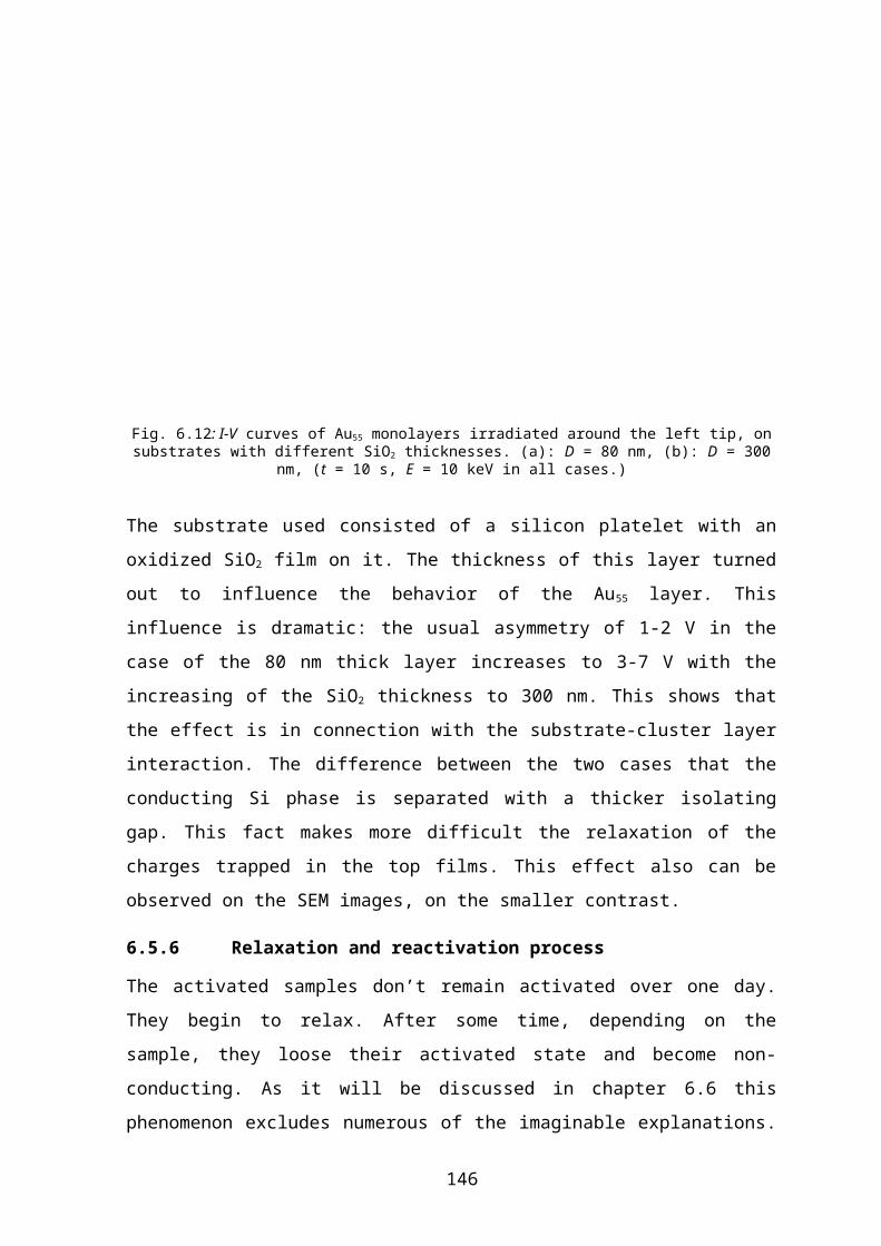
[126] M. Baumle, Dissertation, Universität Essen, (1999)
[127] M. A. Marcus, M. P. Andrews, J. Zegenhagen, A. S. Bommannavar, P. Montano, Phys. Rev. B, 42, 3312, (1990)
[128] L.F. Chi, M. Hartig, T. Drechsler, Th. Schwaack, C. Seidel, H. Fuchs, G.Schmid Appl. Phys. A 66, S187 (1998)
[129] G. Schön, U. Simon, Colloid Polym. Sci. 273: 101, (1995)
[130] G. Schön, U. Simon, Colloid Polym. Sci. 273: 202, (1995)
[131] S.-T. Yau, P. Mulvaney, W. Xu, G. M. Spinks Phys. Rev. B 57, R124-127, (1998)
[132] W. H. Richardson, Appl. Phys. Lett. 71 , 1113, (1997)
[133] G. Schmid L. F. Chi, Adv. Mater. 10 515, (1998)
[134] G. Horhyak, M. Kröll, R. Pugin, T. Sawitowski, G. Schmid, J.-O. Bovin, G. Karsson, H. Hofmeister, S. Hopfe, Chem. Eur. J. 3, 1951, (1997)
[135] O. Vidoni, T. Reuter, V. Torma, W. Mayer-Zaika, G. Schmid, Chem. Mater. Submitted.
[136] S. Peschel, G. Schmid, Angew. Chem. Int. Ed. Engl. 34, 1442, (1995)
[137] G. L. Hornyak, S. Peschel, T. Sawitowski, G. Schmid, Micron, 29, 183, (1998)
[138] H. P. Kormann, Dissertation, Universität Essen, (2001)
[139] G. Schmid, N. Beyer, Eur. J. Inorg. Chem. 835 (2000)
[140] L. Clarke, M. N. Wybourne, M. Yan, S. X. Cai, J. F. W. Keana, Appl. Phys. Lett. 71, 617, (1997)
[141] L. Clarke, M. N. Wybourne, L. O. Brown, J. E. HutchinsonM. Yan, S. X. Cai, J. F. W. Keana, Semicond. Sci. Technol. 13, A111, (1998)
[142] M. P. J. van Staveren, H. B. Brom, L. J. De Jongh, Phys. Rep. 208, 1, (1991)
[143] G. Schmid, Bull. Pol. Acad. Sci. Chem. 46, 229, (1998)
[144] U. Simon, G. Schön, G. Schmid, Angew. Chem. 105, 264, (1993)
148
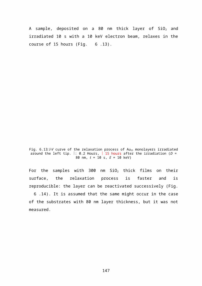
[145] S. Fujita, Synthesis, 423, (1982)
[146] P. D. Caesar, Org. Synth. 693, (1953)
[147] P. D. Caesar, J. Am. Chem. Soc. 73, 1097, (1951)
[148] G. Schmid, N. Klein, L. Korste, U. Kreibig, D. Schönauer, Polyhedron, 7, 605 (1988)
[149] N. F. Mott, Phil. Mag. 19, 835, (1969)
[150] N. F. Mott, E. A. Davis, Electronic Processes in Non-Crystalline Materials, Oxford University Press, Oxford, (1971)
[151] N. F. Mott, Conduction in Non-Crystalline Materials, Clarendon Press, Oxford, (1993)
[152] Hong S, Reifenberger R, w. Tian, S. Datta, J. Henderson, C. P. Kubiak, Superlattices and Microstructures, 28, 289, (2000)
[153] J. R. MacDonald, Impedance Spectroscopy, Wiley New York, (1987).
[154] A. L. Efros, B. I. Shklowskii, Phys. Stat. Solidi, B76, 475. (1976)
[155] M. Schumann, Y. Liu, T. Raschke, C. Radehaus, G. Schmid, Nanoletters, (2001)
[156] D. Knausz, A. Meszticzky, L. Szakács, B. Csákvári, K. Újszászi, J. Organomet. Chem., 256, 11, (1983)
[157] J. E. Morris, T. J. Coutts, Thin Solid films, 47, 3, (1977)
[158] H. Taube, Science, 226, 1028 (1984)
[159] H. Taube, Electron Transfer reactions of Complex Ions in Solution, Academic Press, New York 1970
149
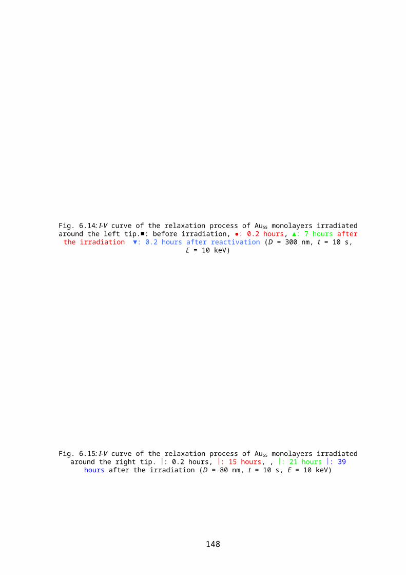
List of the used abbreviations
AFM Atomic Force Microscope
EBL Electron Beam Lithograpy
LB technique Langmuir-Blodgett technique
SEM Scanning Electron Microscope
SET Single Electron Tunneling
Single Electron Transistor
STM Scanning Tunneling Microscope
STS Scanning Tunneling Spectroscopy
TEM Transmission Electron Microscope
150
Zusammenfassung
Einen interessanten Bereich der heutigen Nanotechnologie stellen Untersuchungen an
Clustermaterialen dar, die spezielle elektrische Quanteneffekte („quantum size effect“)
zeigen. Deren potentielle künftige Anwendungen liegen in der „single electron”-
Elektronik. Der Au55 Cluster, beschützt mit unterschiedlichen Ligandhüllen aus phosphor-
und schwefelorganischen Molekülen, ist ein der am besten geeigneten Modellsysteme für
diese Messungen [1].
In der vorliegenden Arbeit wurde auf folgende zwei Schwerpunkte konzentriert. Einerseits
sollten die Einflüsse kovalenter Brücken zwischen den Clustern auf den Ladungstransfer-
Mechanismus der Nanopartikel Systemen, andererseits die Elektronentransport in
geschlossenen Clustermonolagen untersucht werden.
Die heutige Ansicht in der Literatur, ob die Liganden zwischen zwei Clustern den
Ladungstransfer-Mechanismus beeinflussen oder nicht, ist umstritten. Reifenberger und
Mitarbeiter [69] haben es gefunden, dass die chemische Natur der Liganden, insbesondere
deren Endgruppen üben einen Effekt auf die Leitfähigkeit einer Probe aus. Die
Untersuchungen von Simon [114] führten dagegen zum Schluss, dass die
Aktivierungsenergie der Nanopartikel Systeme nur vom Abstand der Nanopartikel, nicht
aber von der chemischen Natur der Liganden abhängt.
Um diesem scheinbaren Widerspruch nachzugehen, wurden die elektrischen Eigenschaften
von zwei-, quasi-zwei-, und dreidimensionalen Au55-Clustersystemen untersucht. Es stellte
sich heraus, dass das Modell von Simon nur für physikalisch verbrückte Systeme gültig ist.
Für kovalent (chemisch) verbrückte Nanopartikel-Systemen ist die Aktivierungsenergie
kleiner als die nach dem erwähnten Modell gewartet und hängt stark von der chemischen
Natur der verbrückenden Liganden ab. Die Aktivierungsenergie zeigt keinen Trend als
Funktion der Interpartikel-Abstand in diesem Fall.
Im letzten Teil der Arbeit wird über elektrische Eigenschaften der Clustermonolagen
berichtet. In den Messungen wurden Si-Plättchen als Trägersubstanz verwendet, mit durch
Elektronenstrahllithographie gebildeten Wolfram Kontakt Strukturen auf der Oberfläche
versehen. Um die Leitfähigkeit der Clustermonolage beobachten zu können, muss die
151
Oberfläche der Probe zu SiO2 oxidiert werden. Es wurde gezeigt, dass das Nanopartikel
System durch Bestrahlung mit Elektronenstrahl aktiviert werden kann. Wir erklären dieses
Phänomen mit dem Überschuss von gefangenen Elektronen in der SiO2 Lage, der durch
positive Bildladungen in die Clusterlage induziert wird. Dieser Effekt bildet die
Elektronenkonfiguration und vielleicht auch die Struktur des Arrangement um.
Asymmetrische Bestrahlung der Lage führt zu eine asymmetrische I-V Charakteristik.
Dieser Befund kann ähnlich erläutert werden, wie das Gleichrichtensverhalten einer
Halbleiterdiode, wobei die Bildladungen in der Clusterlage mit Elektronenlöchern der
Halbleiter in Analogie stehen.
152

Curriculum vitae
NAME: Viktoria Torma
ADRESS: Templomsor u. 38 9081 Győrújbarát, UngarnTel: +0036 30 2439125E-mail: [email protected]
DATE AND PLACE OF BIRTH: 02.03.1975, GyőrPARENTS: Attila Torma, teacher in Győr
Gizella Szelid, teacher in Győr
NATIONALITY: Hungarian
FAMILY CONDITION: Married
LANGUAGES: German, English, Hungarian
Studies1989 – 1993 Miklós Révai High School in Győr
High school graduation: Excellent.
1993 – 1998 Eötvös Loránd University, BudapestChemistry studiesFinal Exam: very goodTitle of the diploma work: Investigation of the Oxygen-Reduction with Impedance SpectroscopySupervisor: Dr. Győző Láng, Assistant Professor at the Eötvös-Uni-versity of Sciences, Budapest.Diploma: very good
Undergraduate research:
1994 – 1996 Investigation of the graphite-water interface with Scanning Tunnelling Spectroscopy Supervisor: Dr. Gabor Nagy, Central Research Insti-tute for Physics, Budapest
1996 – 1998 Investigation of the Oxygen-Reduction on Gold Elec-trode with Impedance SpectroscopySupervisor: Dr. Győző Láng Assistant Professor at the Eötvös-University, Budapest.
1997 Undergraduate Research Conference, I. Pries
1998 – 2002 Ph. D. work in the working group of Prof. Dr. Günter SchmidInstitute for Inorganic Chemistry, University of Essen
153
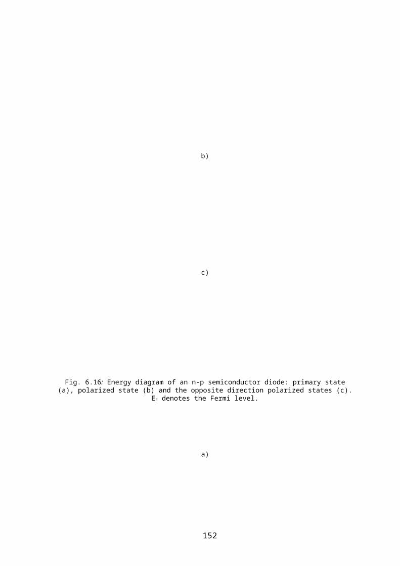
Lebenslauf
NAME: Viktoria Torma
ADRESSE: Templomsor u. 38 9081 Győrújbarát, UngarnTel: +0036 30 2439125E-mail: [email protected]
GEBURTSDATUM und ORT: 02.03.1975, Győr
ELTERN: Attila Torma, Lehrer in GyőrGizella Szelid, Lehrerin in Győr
STAATSANGEHÖRIGKEIT: Ungarisch
FAMILIENSTAND: Verheiratet
SPRACHKENNTNISSE: Deutsch, Englisch, Ungarisch
Studien1989 – 1993 Miklós Révai Gymnasium in Győr
Abitur mit ausgezeichnetem Ergebnis bestanden.
1993 – 1998 Eötvös Loránd Universität, BudapestFachrichtung: ChemieAbschlussprüfung: sehr gutTitel der Diplomarbeit: Untersuchung der Sauerstoffreduktion auf Goldelektrode mit ImpedanzspektroskopieBetreuer: Győző Láng, Dozent an der Eötvös-Universität, Budapest.Diplom: sehr gutQualifikation: Diplom – ChemikerUndergraduate research:
1994 – 1996 Untersuchung der Graphit – Wasser Grenzfläche mit RastertunnelmikroskopieBetreuer: Gabor Nagy, Zentrales Forschungsinstitut für Physik, Budapest
1996 – 1998 Untersuchung der Sauerstoffreduktion auf Goldelektroden mit ImpedanzspektroskopieBetreuer: Győző Láng, Dozent an der Eötvös-Universität, Budapest.
1997 Konferenz des Nationalen Studentenkreises: I. Preis
1998 – 2002 Doktorarbeit bei Prof. Dr. Günter Schmid in Essen,Institut für Anorganische Chemie
154
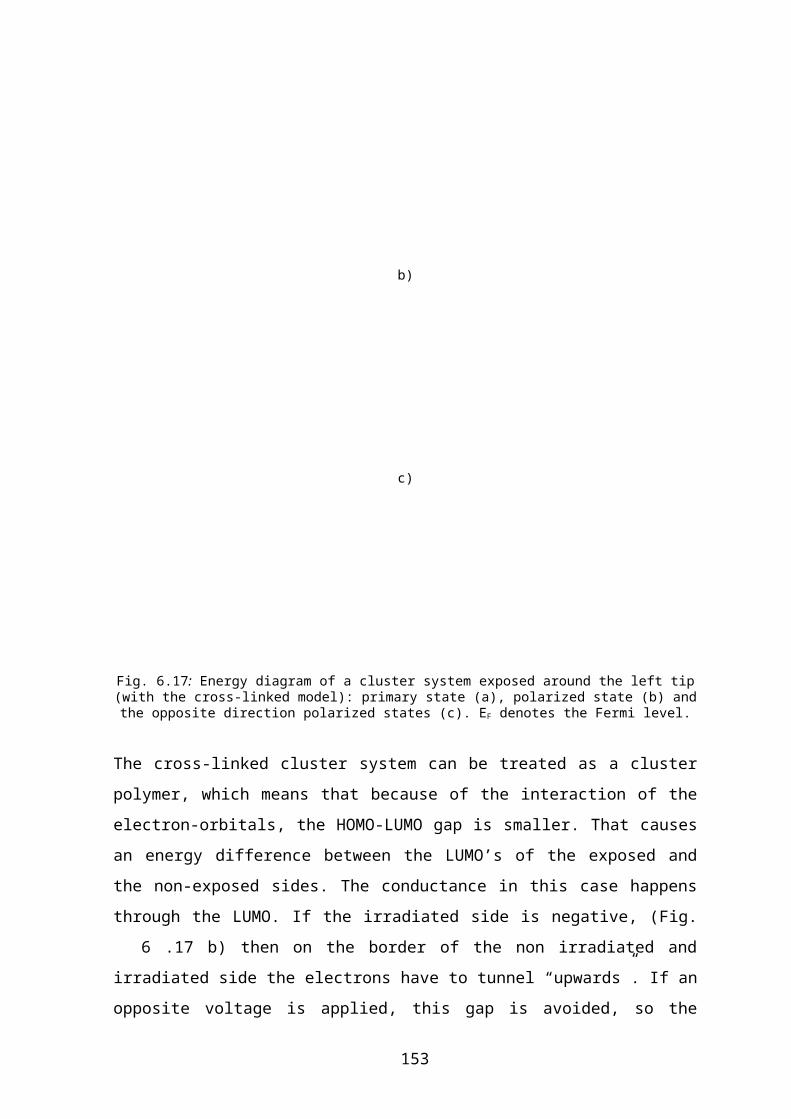
PublikationenStructure/Property – Relations in Au55 Cluster Layers Studied by Temperature De-pendent Impedance MeasurementsViktoria Torma, Günter Schmid Ulrich Simon, ChemPhysChem, 2001 321-325
The Diode Behavior of Asymmetrically Ordered Au55 ClustersViktoria Torma, Matthias Schumann, Christian Radehaus, Günter Schmid, ChemPhysChem, 2001 546-548.
Quasi One-Dimensional Gold Cluster ArrangementsOlivia Vidoni, Torsten Reuter, Viktoria Torma, Wolfgang Meyer-Zaika, Günter Schmid, J. Mater. Chem. 2001 11 .
Die Ergebnisse wurde auch in den folgenden Postern veröffentlicht:
Investigation of Cluster layers by impedance and activation energy measurementsV. Torma, Priv. Doz. U. Simon, Prof. Dr. G. Schmid7th International Symposium on Electrochemical Methods in Corrosion Research Buda-pest, 2000
IInvestigation of Au55 cluster monolayers with electronic measurementsV. Torma, M. Schumann, Dr. Raschke, Prof. Dr. Radehaus, Prof. Dr. G. SchmidSFB 452, Kollective molekulare Ordnungsprozesse in der Chemie. Entstehung, Struktur, Dynamik und Eigenschaften von höher organisierten Systemen, Nov, 2000
Elektrische Eigenschaften von ligandenstabilisierten Au55 Cluster Monolagen V. Torma, M. Schumann, Olivia Vidoni, Torsten Reuter, Yungping Liu, Dr. Raschke, Prof. Dr. Radehaus, Prof. Dr. G. SchmidSFB 452: Begutachtung, März, 2001
Herstellung von neuartigen ein-, zwei- und dreidimensionalen Anordnungen von Au
55-Clustern
V. Torma O. Vidoni, T. Reuter, Y. Liu, M. Schumann, Prof. Dr. G. SchmidSFB 452: Begutachtung, März, 2001
155