DOI: 10.1038/s41467-018-03752-5 OPEN Rolling up transition ...
34
ARTICLE Rolling up transition metal dichalcogenide nanoscrolls via one drop of ethanol Xueping Cui 1,2 , Zhizhi Kong 1 , Enlai Gao 3 , Dazhen Huang 1,2 , Yang Hao 1,2 , Hongguang Shen 1,2 , Chong-an Di 1 , Zhiping Xu 3 , Jian Zheng 1 & Daoben Zhu 1 Two-dimensional transition metal dichalcogenides (TMDs) have attracted lots of interest because of their potential for electronic and optoelectronic applications. Atomically thin TMD flakes were believed capable to scroll into nanoscrolls (NSs) with distinct properties. However, limited by mechanical strength and chemical stability, production of high-quality TMD NSs remains challenging. Here, we scroll chemical vapor deposition-grown monolayer TMD flakes into high-quality NSs in situ in 5 s with a nearly 100% yield by only one droplet of ethanol solution. An obvious photoluminescence is demonstrated in NSs and the self-encapsulated structure makes NSs more insensitive to external factors in optical and electrical properties. Furthermore, based on the internal open topology, NSs hybridized with a variety of functional materials have been fabricated, which is expected to confer TMD NSs with additional properties and functions attractive for potential application. DOI: 10.1038/s41467-018-03752-5 OPEN 1 Beijing National Laboratory for Molecular Sciences, Key Laboratory of Organic Solids, Institute of Chemistry, CAS, Beijing 100190, China. 2 University of Chinese Academy of Sciences, Beijing 100049, China. 3 Department of Engineering Mechanics and Center for Nano and Micro Mechanics, Applied Mechanics Laboratory, Tsinghua University, Beijing 100084, China. Correspondence and requests for materials should be addressed to J.Z. (email: [email protected]) NATURE COMMUNICATIONS | (2018)9:1301 | DOI: 10.1038/s41467-018-03752-5 | www.nature.com/naturecommunications 1 1234567890():,;
Transcript of DOI: 10.1038/s41467-018-03752-5 OPEN Rolling up transition ...
ARTICLE
Rolling up transition metal dichalcogenidenanoscrolls via one drop of ethanolXueping Cui1,2, Zhizhi Kong1, Enlai Gao 3, Dazhen Huang1,2, Yang Hao1,2, Hongguang Shen1,2, Chong-an Di 1,
Zhiping Xu3, Jian Zheng1 & Daoben Zhu1
Two-dimensional transition metal dichalcogenides (TMDs) have attracted lots of interest
because of their potential for electronic and optoelectronic applications. Atomically thin TMD
flakes were believed capable to scroll into nanoscrolls (NSs) with distinct properties.
However, limited by mechanical strength and chemical stability, production of high-quality
TMD NSs remains challenging. Here, we scroll chemical vapor deposition-grown monolayer
TMD flakes into high-quality NSs in situ in 5 s with a nearly 100% yield by only one droplet
of ethanol solution. An obvious photoluminescence is demonstrated in NSs and the
self-encapsulated structure makes NSs more insensitive to external factors in optical and
electrical properties. Furthermore, based on the internal open topology, NSs hybridized with a
variety of functional materials have been fabricated, which is expected to confer TMD NSs
with additional properties and functions attractive for potential application.
DOI: 10.1038/s41467-018-03752-5 OPEN
1 Beijing National Laboratory for Molecular Sciences, Key Laboratory of Organic Solids, Institute of Chemistry, CAS, Beijing 100190, China. 2 University ofChinese Academy of Sciences, Beijing 100049, China. 3Department of Engineering Mechanics and Center for Nano and Micro Mechanics, AppliedMechanics Laboratory, Tsinghua University, Beijing 100084, China. Correspondence and requests for materials should be addressed toJ.Z. (email: [email protected])
NATURE COMMUNICATIONS | (2018) 9:1301 | DOI: 10.1038/s41467-018-03752-5 |www.nature.com/naturecommunications 1
1234
5678
90():,;
Atomically two-dimensional (2D) transition metal dichal-cogenides (TMDs), such as MoS2, MoSe2, WS2, and WSe2,display numerous exceptional electronic and optical
properties arising from quantum confinement1,2. Complementaryto gapless graphene, 2D TMDs with intrinsic band gapsare promising interesting field-effect transistor (FET) andoptoelectronic devices. Recently, the main focus of attention hasbeen for the production of their intrinsic or heterojunctionstructures, their properties, and their applications on 2D scale3–8.In addition to changes in 2D size and form, self-assembly of theatomically thin TMD flakes, as an emerging area, is largelyunexplored. Assembly processes by folding and scrolling, i.e.,rolling up, can transform relatively simple structures into com-plex topologies, such as nanoscrolls (NSs), with distinct proper-ties as well as the original excellent characteristics. Indeed,theoretical calculations have predicted the unique topology of 2Dmaterial-based NSs to yield unusual electronic and opticalproperties9–12; thus these NSs have promise as building blocks inflexible electronics, microfluidics, energy storage, self-propelledmicromachines, and optical resonators13–18. However, experi-mental realization of such high-quality NSs has only beenachieved for graphene13–16 and boron nitride19, which exhibitedhigh strength and chemical inertness. Limitations in mechanicalstrength and chemical stability present difficulties in producinghigh-quality TMD-NSs20. Recently, an argon plasma-assistedmethod has been demonstrated for the fabrication of amorphousMoS2-NSs, but in this method MoS2 sheets failed to scrolleffectively, only edge region of the sheet curved while the largecentral area remains plane. Moreover, upon argon plasmaetching, a serious damage has been brought to the original sheets,where almost half of sulfur atoms were removed. The obtainedNSs exhibited low crystallinity even to be amorphous21. A high-quality TMD-NS is highly desirable for both fundamental studiesand potential applications; however, its reliable experimentalfabrication still remains challenging.
Here, we show a very simple method for fabricating high-quality TMD-NSs, which only requires one droplet of ethanolsolution to scroll chemical vapor deposition (CVD)-grownmonolayer TMD flakes in situ in 5 s with a nearly 100% yield.TMD-NSs are promising optoelectronic materials with potentialapplications in optoelectronic devices because of the high FETmobility. Owing to self-encapsulated structure, the optical andelectrical properties of NSs are more insensitive to external fac-tors, while the electrical performance of 2D materials flakes varieswith both the underlying substrate and the environment. Inaddition, because of the internal open topology, the interlayer
spacing of TMD-NSs can be easily expanded to accommodate avariety of functional materials, including organic small molecules,polymers, nanoparticles, and 2D materials, as well as biologicalsubstances. These features are very attractive for applications insolar cells, photodetectors, flexible logic circuits, energy storage,and sensors.
ResultsRolling up CVD-grown TMD monolayer flakes. In a typicalexperiment, large-area, monolayer TMD flakes were synthesizedon a SiO2/Si substrate by CVD. Then, the TMD flakes werescrolled into NSs in just 5 s with a nearly 100% yield by placingone drop of ethanol solution (volume ratio of ethanol:water=2:1) on their surface. Other aqueous solutions, such as methanol,tetrahydrofuran, dimethylformamide, and N-methyl-2-pyrroli-done, can also be used for TMD flakes scrolling (SupplementaryFig. 1, 2 and Supplementary Note 1). In addition, the scrollingproceeded well for TMD flakes grown on other substrates, such asSi3N4 and sapphire (Supplementary Fig. 3). To clarify the TMD-NSs formation process, the entire procedure was recorded using aCCD camera equipped on an optical-microscope (SupplementaryMovie 1). A series of steps that might have led to the formation ofthe TMD-NSs are proposed in Fig. 1. Monolayer TMD flakeswere grown on a substrate at a high temperature ( ≥ 720 °C).During the process of cooling down to room temperature, a strainwas introduced to the TMD flakes because of the mismatch inthermal expansion coefficients between the TMD flake and thesubstrate. Stable TMD flakes were achieved when the strain andsubstrate adhesion were balanced. When an ethanol solutionspread onto the surface of TMD flakes, the liquid film intercalatedinto the TMD flakes and the substrate, as demonstrated by thecontrast color change in the flakes (Supplementary Fig. 4). Withthe liquid intercalation, part of the TMD flake was first releasedfrom the substrate to become freestanding as shown in Fig. 1.Under the built-in strain, the released part of the flake curved outof the plane and continued to roll up to a complete NS in thesolution. An energy analysis of the MoS2 flakes before and afterscrolling was presented in the Supplementary Note 2. The energybarrier required to bend the freestanding flake out of plane wasproved to be relatively low, indicating the easy nucleation of ascroll. In addition, the strain energy induced from the thermalmismatch of the MoS2 flake was found high enough to activatethe formation of scrolls after the liquid intercalation and theadhesion energy of the MoS2 flake with substrate decreasing(Supplementary Fig. 5). Strain as the stimulus to the NSs
HT
RTStrain Strain
StrainStrain
Adhesion Adhesion
Adhesion No Adhesion =Mo, W =S, Se =wafer =liquid
Fig. 1 Schematic of self-scrolling of chemical vapor deposition (CVD)-based transition metal dichalcogenide (TMD) monolayer flakes. A proposed series ofsteps leading to the formation of TMD-NSs is shown: (I) initial TMD monolayer growth on a substrate at a high temperature (HT) (e.g., 720, 825 °C); (II)the generation of a strain, balanced with the adhesion from substrate, in the TMD monolayer while cooling down to room temperature (RT); (III) theinsertion of liquid between the TMD monolayer and substrate and the disappearance of the adhesion; (IV) the TMD flakes curve out of the plane driven bythe strain; (V) the final formation of TMD-NSs
ARTICLE NATURE COMMUNICATIONS | DOI: 10.1038/s41467-018-03752-5
2 NATURE COMMUNICATIONS | (2018) 9:1301 | DOI: 10.1038/s41467-018-03752-5 | www.nature.com/naturecommunications
formation was also suggested by the following fact. When treatedwith ethanol solution, freshly produced TMD flakes on substrateswere more prone to scroll in the shortest time with the highestyield, while the aged samples exhibited slightly decreased scrollingspeed and yield. A few cracks were observed in aged samples byscanning electron microscopy (SEM, Supplementary Fig. 6), andthese cracks could have partially relieved the strain.
TMD flakes were observed to prefer to scroll along one edgewhere the adhesion with the substrate was first relaxed upon theintercalation of the liquid. As the edges of CVD-grown TMDsingle crystals have a zigzag orientation4,22,23, the chirality of theirNSs are defined (Supplementary Fig. 7). For large-area poly-crystalline films without regular edges, the orientation andchirality of their NSs are generally random (Fig. 2a, b). Thus,the controllable scrolling of TMD films was attempted (Fig. 2c–eand Supplementary Fig. 8). Using a focused ion beam (FIB), aMoS2 polycrystalline film was patterned into parallel ribbons withdefined width and direction (Fig. 2c) to produce long NS arrays(Fig. 2d). Using FIB etching a second time, long NSs were furtherarranged into periodic arrays with a controlled length (Fig. 2e).These NS arrays have promise for wide application, such asintegrated circuits and matrix displays. We assume thathorizontal TMD-NS arrays with controllable chirality couldpotentially be achieved by controlling the crystal orientation ofthe ribbon edges via etching from one large-area TMD single
crystal, which is prevented by the technique to synthesize large-area TMD single crystals.
Morphology characterization. CVD-grown TMD flakes are highquality even comparable to intrinsic flakes23,24. The ethanolsolution was clean and harmless; therefore, no defects or impu-rities were introduced into the high-quality TMD-NSs (Supple-mentary Fig. 9). Based on this method, several typical TMD-NSs,including those of MoS2 (Fig. 2f and Supplementary Fig. 10), WS2(Fig. 2g), MoSe2 (Fig. 2h), and WSe2 (Fig. 2i), were successfullyfabricated. Most of the NSs displayed a straight and compactappearance. High-resolution transmission electron microscopy(HR-TEM) was used to further examine the TMD-NSs micro-structure, which was found to be multiwalled and tubular(Fig. 2j–m). The diameter and sidewall thickness of the TMD-NSvaried with the size of the original flake. The hollow diameterswere 10–40 nm. In addition, the high-magnification images of thesidewalls and the selected area electron diffraction (SAED) bothshowed that the TMD layers in the NSs were stacked uniformlyand compactly (Fig. 2j–m inset and Supplementary Fig. 11). Thedistance between adjacent walls was approximately 6.21 Å, 6.41 Å,6.35 Å, and 6.45 Å for MoS2-, WS2-, MoSe2-, and WSe2-NSs,respectively, which matched the interlayer spacing in bulk TMDs(6.15 Å, 6.36 Å, 6.45 Å, and 6.49 Å for MoS2, WS2, MoSe2, and
a b c d e
f g h i
j k l m6.21 Å 6.41 Å 6.35 Å 6.45 Å
Fig. 2 Transition metal dichalcogenide (TMD)-nanoscrolls (NSs) from self-scrolling chemical vapor deposition (CVD)-based TMD monolayer flakes. aOptical image of CVD-grown MoS2 monolayer flakes on a SiO2/Si substrate (the purple area represents the substrate, the green area represents the MoS2monolayers; scale bar, 500 μm). b Optical image of MoS2-NSs on a SiO2/Si substrate (scale bar, 100 μm). c–e The fabrication process of a MoS2-NS array(scanning electron microscopy—SEM image shown, scale bars, 50 μm). c Large-area MoS2 monolayer film patterned into ribbons by focused ion beam(FIB) etching (the dark region represents MoS2 film, the bright area is bare substrate). d Long MoS2-NSs made from the controllable scrolling of thepatterned MoS2 film in c. (The white parallel lines are MoS2-NSs, and the dark area represents the substrate). e A 12 × 6 array of MoS2-NSs fabricated via asecond FIB etching of the long MoS2-NSs in d. f–i SEM images of typical TMD-NSs on SiO2/Si substrates: MoS2-NSs (f),WS2-NSs (g), MoSe2-NSs (h), andWSe2-NSs (i). (Scale bars, 5 μm in f, i and 10 μm in g, h). j–m TEM images of typical TMD-NSs: MoS2-NSs (j),WS2-NSs (k), MoSe2-NSs (l), and WSe2-NSs(m). (Scale bars, 20 nm). Inset: High-magnification images of sidewalls of TMD-NSs (scale bars, 2 nm)
NATURE COMMUNICATIONS | DOI: 10.1038/s41467-018-03752-5 ARTICLE
NATURE COMMUNICATIONS | (2018) 9:1301 | DOI: 10.1038/s41467-018-03752-5 |www.nature.com/naturecommunications 3
WSe2, respectively), indicating both the tight scrolling of theTMD flakes and the lack of interlayer contamination.
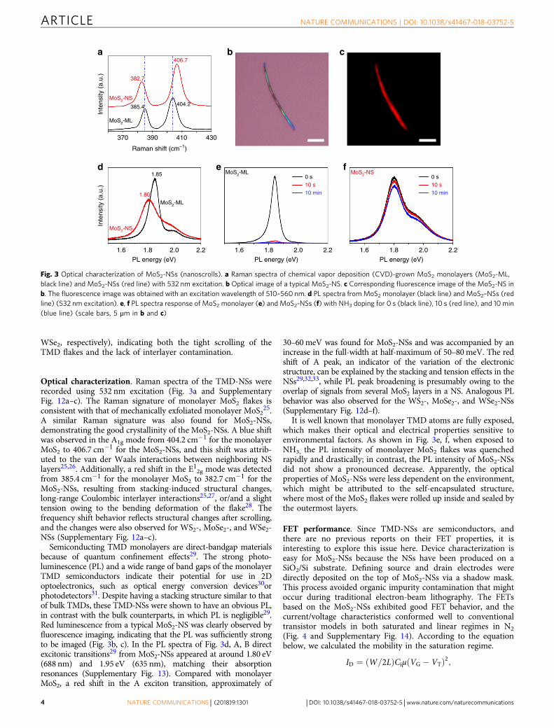
Optical characterization. Raman spectra of the TMD-NSs wererecorded using 532 nm excitation (Fig. 3a and SupplementaryFig. 12a–c). The Raman signature of monolayer MoS2 flakes isconsistent with that of mechanically exfoliated monolayer MoS225.A similar Raman signature was also found for MoS2-NSs,demonstrating the good crystallinity of the MoS2-NSs. A blue shiftwas observed in the A1g mode from 404.2 cm−1 for the monolayerMoS2 to 406.7 cm−1 for the MoS2-NSs, and this shift was attrib-uted to the van der Waals interactions between neighboring NSlayers25,26. Additionally, a red shift in the E12g mode was detectedfrom 385.4 cm−1 for the monolayer MoS2 to 382.7 cm−1 for theMoS2-NSs, resulting from stacking-induced structural changes,long-range Coulombic interlayer interactions25,27, or/and a slighttension owing to the bending deformation of the flake28. Thefrequency shift behavior reflects structural changes after scrolling,and the changes were also observed for WS2-, MoSe2-, and WSe2-NSs (Supplementary Fig. 12a–c).
Semiconducting TMD monolayers are direct-bandgap materialsbecause of quantum confinement effects29. The strong photo-luminescence (PL) and a wide range of band gaps of the monolayerTMD semiconductors indicate their potential for use in 2Doptoelectronics, such as optical energy conversion devices30orphotodetectors31. Despite having a stacking structure similar to thatof bulk TMDs, these TMD-NSs were shown to have an obvious PL,in contrast with the bulk counterparts, in which PL is negligible29.Red luminescence from a typical MoS2-NS was clearly observed byfluorescence imaging, indicating that the PL was sufficiently strongto be imaged (Fig. 3b, c). In the PL spectra of Fig. 3d, A, B directexcitonic transitions29 from MoS2-NSs appeared at around 1.80 eV(688 nm) and 1.95 eV (635 nm), matching their absorptionresonances (Supplementary Fig. 13). Compared with monolayerMoS2, a red shift in the A exciton transition, approximately of
30–60meV was found for MoS2-NSs and was accompanied by anincrease in the full-width at half-maximum of 50–80meV. The redshift of A peak, an indicator of the variation of the electronicstructure, can be explained by the stacking and tension effects in theNSs29,32,33, while PL peak broadening is presumably owing to theoverlap of signals from several MoS2 layers in a NS. Analogous PLbehavior was also observed for the WS2-, MoSe2-, and WSe2-NSs(Supplementary Fig. 12d–f).
It is well known that monolayer TMD atoms are fully exposed,which makes their optical and electrical properties sensitive toenvironmental factors. As shown in Fig. 3e, f, when exposed toNH3, the PL intensity of monolayer MoS2 flakes was quenchedrapidly and drastically; in contrast, the PL intensity of MoS2-NSsdid not show a pronounced decrease. Apparently, the opticalproperties of MoS2-NSs were less dependent on the environment,which might be attributed to the self-encapsulated structure,where most of the MoS2 flakes were rolled up inside and sealed bythe outermost layers.
FET performance. Since TMD-NSs are semiconductors, andthere are no previous reports on their FET properties, it isinteresting to explore this issue here. Device characterization iseasy for MoS2-NSs because the NSs have been produced on aSiO2/Si substrate. Defining source and drain electrodes weredirectly deposited on the top of MoS2-NSs via a shadow mask.This process avoided organic impurity contamination that mightoccur during traditional electron-beam lithography. The FETsbased on the MoS2-NSs exhibited good FET behavior, and thecurrent/voltage characteristics conformed well to conventionaltransistor models in both saturated and linear regimes in N2
(Fig. 4 and Supplementary Fig. 14). According to the equationbelow, we calculated the mobility in the saturation regime.
ID ¼ W=2Lð ÞCiμ VG � VTð Þ2;
Inte
nsity
(a.
u.)
Inte
nsity
(a.
u.)
Raman shift (cm–1)
370 390 410 430
MoS2-NS
MoS2-NS
MoS2-NS
MoS2-ML
MoS2-ML
MoS2-ML
382.7
385.4 404.2
406.7
1.85
1.80
0 s10 s10 min
0 s10 s10 min
1.6 1.8 2.0 2.2
PL energy (eV)
1.6 1.8 2.0 2.2
PL energy (eV)
1.6 1.8 2.0 2.2
PL energy (eV)
a b c
d e f
Fig. 3 Optical characterization of MoS2-NSs (nanoscrolls). a Raman spectra of chemical vapor deposition (CVD)-grown MoS2 monolayers (MoS2-ML,black line) and MoS2-NSs (red line) with 532 nm excitation. b Optical image of a typical MoS2-NS. c Corresponding fluorescence image of the MoS2-NS inb. The fluorescence image was obtained with an excitation wavelength of 510–560 nm. d PL spectra from MoS2 monolayer (black line) and MoS2–NSs (redline) (532 nm excitation). e, f PL spectra response of MoS2 monolayer (e) and MoS2-NSs (f) with NH3 doping for 0 s (black line), 10 s (red line), and 10min(blue line) (scale bars, 5 μm in b and c)
ARTICLE NATURE COMMUNICATIONS | DOI: 10.1038/s41467-018-03752-5
4 NATURE COMMUNICATIONS | (2018) 9:1301 | DOI: 10.1038/s41467-018-03752-5 | www.nature.com/naturecommunications
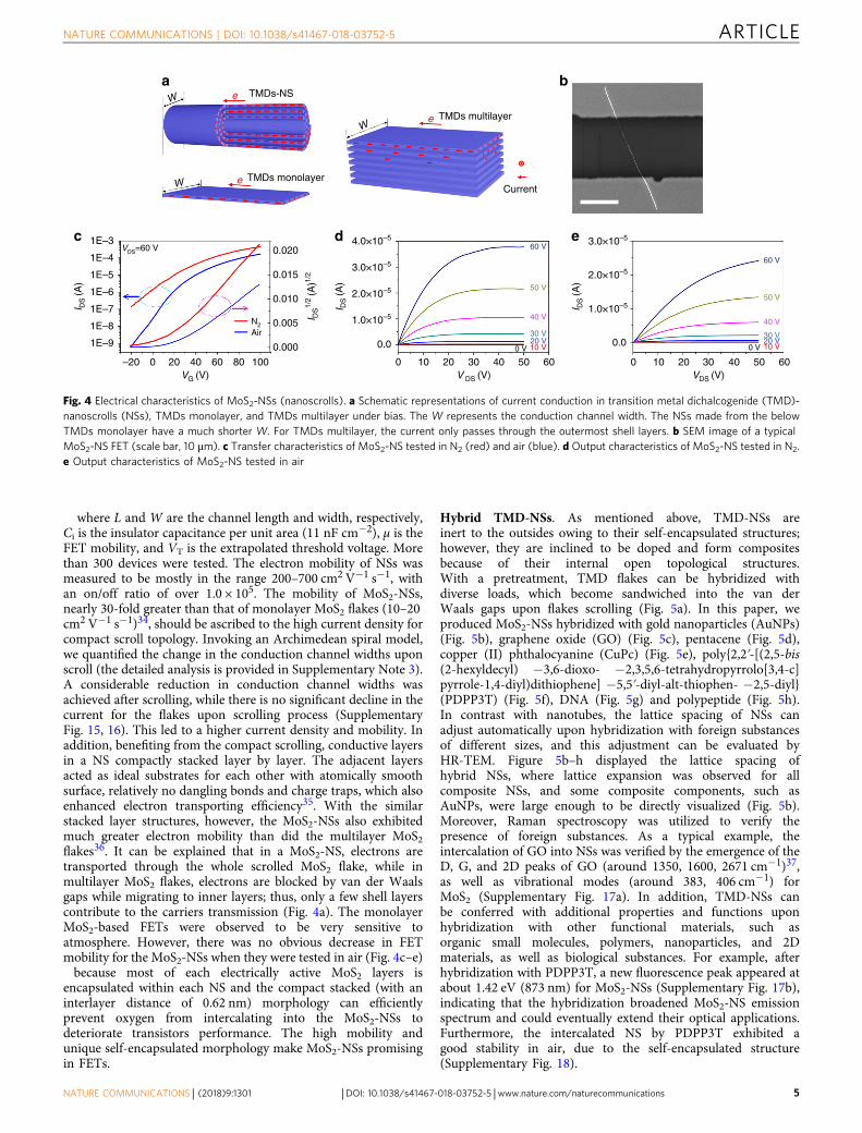
where L and W are the channel length and width, respectively,Ci is the insulator capacitance per unit area (11 nF cm−2), µ is theFET mobility, and VT is the extrapolated threshold voltage. Morethan 300 devices were tested. The electron mobility of NSs wasmeasured to be mostly in the range 200–700 cm2 V−1 s−1, withan on/off ratio of over 1.0 × 10⁵. The mobility of MoS2-NSs,nearly 30-fold greater than that of monolayer MoS2 flakes (10–20cm2 V−1 s−1)34, should be ascribed to the high current density forcompact scroll topology. Invoking an Archimedean spiral model,we quantified the change in the conduction channel widths uponscroll (the detailed analysis is provided in Supplementary Note 3).A considerable reduction in conduction channel widths wasachieved after scrolling, while there is no significant decline in thecurrent for the flakes upon scrolling process (SupplementaryFig. 15, 16). This led to a higher current density and mobility. Inaddition, benefiting from the compact scrolling, conductive layersin a NS compactly stacked layer by layer. The adjacent layersacted as ideal substrates for each other with atomically smoothsurface, relatively no dangling bonds and charge traps, which alsoenhanced electron transporting efficiency35. With the similarstacked layer structures, however, the MoS2-NSs also exhibitedmuch greater electron mobility than did the multilayer MoS2flakes36. It can be explained that in a MoS2-NS, electrons aretransported through the whole scrolled MoS2 flake, while inmultilayer MoS2 flakes, electrons are blocked by van der Waalsgaps while migrating to inner layers; thus, only a few shell layerscontribute to the carriers transmission (Fig. 4a). The monolayerMoS2-based FETs were observed to be very sensitive toatmosphere. However, there was no obvious decrease in FETmobility for the MoS2-NSs when they were tested in air (Fig. 4c–e)because most of each electrically active MoS2 layers is
encapsulated within each NS and the compact stacked (with aninterlayer distance of 0.62 nm) morphology can efficientlyprevent oxygen from intercalating into the MoS2-NSs todeteriorate transistors performance. The high mobility andunique self-encapsulated morphology make MoS2-NSs promisingin FETs.
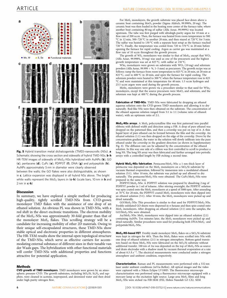
Hybrid TMD-NSs. As mentioned above, TMD-NSs areinert to the outsides owing to their self-encapsulated structures;however, they are inclined to be doped and form compositesbecause of their internal open topological structures.With a pretreatment, TMD flakes can be hybridized withdiverse loads, which become sandwiched into the van derWaals gaps upon flakes scrolling (Fig. 5a). In this paper, weproduced MoS2-NSs hybridized with gold nanoparticles (AuNPs)(Fig. 5b), graphene oxide (GO) (Fig. 5c), pentacene (Fig. 5d),copper (II) phthalocyanine (CuPc) (Fig. 5e), poly{2,2ʹ-[(2,5-bis(2-hexyldecyl) −3,6-dioxo- −2,3,5,6-tetrahydropyrrolo[3,4-c]pyrrole-1,4-diyl)dithiophene] −5,5ʹ-diyl-alt-thiophen- −2,5-diyl}(PDPP3T) (Fig. 5f), DNA (Fig. 5g) and polypeptide (Fig. 5h).In contrast with nanotubes, the lattice spacing of NSs canadjust automatically upon hybridization with foreign substancesof different sizes, and this adjustment can be evaluated byHR-TEM. Figure 5b–h displayed the lattice spacing ofhybrid NSs, where lattice expansion was observed for allcomposite NSs, and some composite components, such asAuNPs, were large enough to be directly visualized (Fig. 5b).Moreover, Raman spectroscopy was utilized to verify thepresence of foreign substances. As a typical example, theintercalation of GO into NSs was verified by the emergence of theD, G, and 2D peaks of GO (around 1350, 1600, 2671 cm−1)37,as well as vibrational modes (around 383, 406 cm−1) forMoS2 (Supplementary Fig. 17a). In addition, TMD-NSs canbe conferred with additional properties and functions uponhybridization with other functional materials, such asorganic small molecules, polymers, nanoparticles, and 2Dmaterials, as well as biological substances. For example, afterhybridization with PDPP3T, a new fluorescence peak appeared atabout 1.42 eV (873 nm) for MoS2-NSs (Supplementary Fig. 17b),indicating that the hybridization broadened MoS2-NS emissionspectrum and could eventually extend their optical applications.Furthermore, the intercalated NS by PDPP3T exhibited agood stability in air, due to the self-encapsulated structure(Supplementary Fig. 18).
a
edc 1E–3
1E–4
1E–5
1E–6
1E–7
1E–8
1E–9
–20 0 20 40 60 80 100
0.020
0.015
0.010
0.005
0.000
VDS=60 V
I DS
(A)
I DS
1/2
(A)1/
2
VG (V)
AirN2
I DS
(A)
I DS
(A)
4.0×10⁻⁵
3.0×10⁻⁵
2.0×10⁻⁵
1.0×10⁻⁵
0.0
3.0×10⁻⁵
2.0×10⁻⁵
1.0×10⁻⁵
0.0
0 10 20 30 40 50 60V DS (V)
60 V
50 V
40 V
30 V20 V10 V0 V
0 10 20 30 40 50 60VDS (V)
60 V
50 V
40 V
30 V20 V10 V0 V
W
W
W
e
e
e
TMDs-NS
TMDs monolayer
TMDs multilayer
Current
b
Fig. 4 Electrical characteristics of MoS2-NSs (nanoscrolls). a Schematic representations of current conduction in transition metal dichalcogenide (TMD)-nanoscrolls (NSs), TMDs monolayer, and TMDs multilayer under bias. The W represents the conduction channel width. The NSs made from the belowTMDs monolayer have a much shorter W. For TMDs multilayer, the current only passes through the outermost shell layers. b SEM image of a typicalMoS2-NS FET (scale bar, 10 μm). c Transfer characteristics of MoS2-NS tested in N2 (red) and air (blue). d Output characteristics of MoS2-NS tested in N2.e Output characteristics of MoS2-NS tested in air
NATURE COMMUNICATIONS | DOI: 10.1038/s41467-018-03752-5 ARTICLE
NATURE COMMUNICATIONS | (2018) 9:1301 | DOI: 10.1038/s41467-018-03752-5 |www.nature.com/naturecommunications 5
DiscussionIn summary, we have explored a simple method for producinghigh-quality, tightly scrolled TMD-NSs from CVD-grownmonolayer TMD flakes with the assistance of one drop of anethanol solution. An obvious PL was shown in TMD-NSs, with ared shift in the direct excitonic transitions. The electron mobilityof the MoS2-NSs was approximately 30-fold greater than that ofthe monolayer MoS2 flakes. This scrolling strategy will be acandidate for increasing mobility of other 2D materials. Owing totheir unique self-encapsulated structures, these TMD-NSs showstable optical and electronic properties in different atmospheres.The HR-TEM results show the internal open topological structureof the TMD-NSs, which serve as effective carriers for accom-modating external substance of different sizes in their tunable vander Waals gaps. The hybridization with other functional materialswill confer TMD-NSs with additional properties and functionsattractive for potential application.
MethodsCVD growth of TMD monolayers. TMD monolayers were grown by an atmo-spheric pressure CVD. The growth substrates, including SiO2/Si, Si3N4 and sap-phire, were cleaned in acetone, isopropanol, and deionized water and then driedunder high-purity nitrogen flow.
For MoS2 monolayers, the growth substrate was placed face-down above aceramic boat containing MoO3 powder (Sigma Aldrich, 99.998%, 20 mg). Theceramic boat was then loaded in the heating zone center of the furnace tube, whereanother boat containing 80 mg of sulfur (Alfa Aesar, 99.999%) was locatedupstream. The tube was first purged with ultrahigh-purity argon for 10 min at aflow rate of 200 sccm. Then, the furnace was heated from room temperature to 500°C in 12 min, 500–720 °C in another 20 min, and then stayed at 720 °C for 5 min.The sulfur was heated to 130 °C with a separate heat setup as the furnace reached720 °C. Finally, the temperature was cooled from 720 to 570 °C in 20 min beforeopening the furnace for rapid cooling. Argon as carrier gas was maintained at aflow rate of 10 sccm throughout the growth process.
The growth of WS2 monolayers was similar to that of MoS2, except that WO3
(Alfa Aesar, 99.998%, 10 mg) was used as one of the precursors and the highestgrowth temperature was set at 825 °C, with sulfur at 150 °C.
WSe2 monolayers were grown on substrates with WO3 (10 mg) and seleniumpowders (Alfa Aesar, 99.999+%, 1–5 mm) as precursors. The growth recipe was asfollows: ramp the furnace from room temperature to 825 °C in 20 min, sit 20 min at825 °C, cool to 600 °C in 20 min, and open the furnace for rapid cooling. Theselenium powders were heated to 300 °C when the furnace temperature rose to 825°C and were maintained at this temperature for 40 min. 1.5 sccm hydrogen and23.5 sccm argon were used during the growth process.
MoSe2 monolayers were grown via a procedure similar to that used for WSe2monolayers, except that the source precursors were MoO3 and selenium, and theselenium was kept at 400 °C during the growth process.
Fabrication of TMD-NSs. TMD-NSs were fabricated by dropping an ethanolaqueous solution onto the CVD-grown TMD monolayers and allowing it to drynaturally. Rod-like NSs were then obtained on the substrate. The concentration ofthe ethanol aqueous solution ranged from 5:1 to 1:1 (volume ratio of ethanol:water), with an optimum ratio of 2:1.
MoS2-NSs arrays. A MoS2 polycrystalline film was first patterned into parallelribbons with defined width and direction using a FIB. A drop of pure ethanol wasdropped on the patterned film, and then a coverslip was put on top of it. A thinliquid layer of pure ethanol can be formed between the film and the coverslip. Anethanol solution (1:1) was then dropped on the edge of the coverslip. Drove by theconcentration gradient, the water in the solution will slowly infiltrate into the pureethanol under the coverslip in the gradient direction (as shown in SupplementaryFig. 8). The diffusion rate can be adjusted by the concentration of the ethanolsolution. In this way one side of a ribbon was first controlled to scroll to produce along NS. The long NS array was then fabricated and further arranged into periodicarrays with a controlled length by FIB etching a second time.
Hybrid MoS2-NSs fabrication. Pentacene/MoS2-NSs: a 1-nm-thick layer ofpentacene was deposited on the MoS2 monolayers on a SiO2/Si substrate byvacuum thermal evaporation, followed by immersion into a modulated ethanolsolution (5:1). After 10 min, the substrate was picked up and allowed to drynaturally. The pentacene/MoS2-NSs were obtained. The CuPc/MoS2-NSs wereprepared in the same way.
PDPP3T/MoS2-NSs: A PDPP3T solution was prepared by dissolving 2 mg ofPDPP3T powder in 1 ml of toluene. After stirring overnight, the PDPP3T solutionwas spin-coated onto the MoS2 monolayers at a speed of 5000 rpm. After annealingat 70 °C for 20 min, the PDPP3T-coated MoS2 monolayers were then dipped intoan ethanol solution (5:1). After 10 min, the MoS2 monolayers were picked up anddried naturally.
GO/MoS2-NSs: This procedure is similar to that used for PDPP3T/MoS2-NSs.Freshly exfoliated GO sheets were dispersed in n-hexane and then spin-coated ontoMoS2 monolayers. After dropping an ethanol solution (2:1) onto the samples, theGO/MoS2-NSs were obtained.
Au/MoS2-NSs: MoS2 monolayers were dipped into an ethanol solution (2:1)containing AuNPs. Ten minutes later, the MoS2 monolayers were picked up anddried naturally. Similar procedures were used for producing both DNA/MoS2- andpolypetide/MoS2-NSs.
MoS2-NS-based FET. Freshly made monolayer MoS2 flakes on a SiO2/Si substratewere kept in nitrogen for 48 h. Then the MoS2 flakes were scrolled into NSs withone drop of ethanol solution (2:1) in nitrogen atmosphere. Bottom-gated transis-tors based on these MoS2-NSs were fabricated on the SiO2/Si substrate withoutadditional transfer. 100 nm of Au was deposited on the top of MoS2-NSs as sourceand drain electrodes with a shadow mask by vacuum thermal evaporation at a rateof about 0.3 Å s−1. The electrical measurements were conducted under a nitrogenatmosphere and ambient condition, respectively.
Characterization. Raman and PL measurements were performed with a 532 nmlaser under ambient conditions (inVia-Reflex). All optical images and the videowere captured with a Nikon Eclipse LV100D. The fluorescence microscopecharacterization was performed using a fluorescence microscope equipped with amercury lamp as the excitation light source. Large-area MoS2 films and longMoS2-NSs were etched via FIB-SEM (FEI, Helios Nanolab G3 CX). SEM
Mo, W S, Se Functional materials
12
.6 Å
11.6
Å
10.6
Å12
.5 Å
15.7
Å
14.3
Å
a b
c d e
f g h
Fig. 5 Hybrid transition metal dichalcogenide (TMD)-nanoscrolls (NSs). aSchematic showing the cross section and sidewalls of hybrid TMD-NSs. b–hHR-TEM images of sidewalls of MoS2-NSs hybridized with AuNPs (b), GO(c), pentacene (d), CuPc (e), PDPP3T (f), DNA (g) and polypeptide (h).AuNPs approximately 5 nm in diameter were clearly observedbetween the walls; the GO flakes were also distinguishable, as shownin c. Lattice expansion was displayed in all hybrid NSs above. The brightwhite walls represent the MoS2 layers in (c–h) (scale bars, 10 nm in b and2 nm in c–h)
ARTICLE NATURE COMMUNICATIONS | DOI: 10.1038/s41467-018-03752-5
6 NATURE COMMUNICATIONS | (2018) 9:1301 | DOI: 10.1038/s41467-018-03752-5 | www.nature.com/naturecommunications
(Hitachi S-4800) and HR-TEM (JEOL JEM-2100F) were employed to image thesamples. Current–voltage curves were obtained by a three-probe station under anitrogen atmosphere and ambient conditions (Keithley 4200 SCS).
Data availability. The data that support the findings of this study are availablefrom the corresponding author on reasonable request.
Received: 24 August 2017 Accepted: 8 March 2018
References1. Wang, Q. H., Kalantar-Zadeh, K., Kis, A., Coleman, J. N. & Strano, M. S.
Electronics and optoelectronics of two-dimensional transition metaldichalcogenides. Nat. Nanotechnol. 7, 699–712 (2012).
2. Chhowalla, M. et al. The chemistry of two-dimensional layered transitionmetal dichalcogenide nanosheets. Nat. Chem. 5, 263–275 (2013).
3. Kang, K. et al. High-mobility three-atom-thick semiconducting films withwafer-scale homogeneity. Nature 520, 656–660 (2015).
4. Chen, J. et al. Chemical vapor deposition of large-size monolayer MoSe2crystals on molten glass. J. Am. Chem. Soc. 139, 1073–1076 (2017).
5. Gong, Y. et al. Vertical and in-plane heterostructures from WS2/MoS2monolayers. Nat. Mater. 13, 1135–1142 (2014).
6. Duan, X. et al. Lateral epitaxial growth of two-dimensional layeredsemiconductor heterojunctions. Nat. Nanotechnol. 9, 1024–1030 (2014).
7. Li, M. Y. et al. Epitaxial growth of a monolayer WSe2-MoS2 lateral pn junctionwith an atomically sharp interface. Science 349, 524–528 (2015).
8. Li, X. et al. Two-dimensional GaSe/MoSe2 misfit bilayer heterojunctions byvan der Waals epitaxy. Sci. Adv. 2, e1501882 (2016).
9. Pan, H., Feng, Y. & Lin, J. Ab initio study of electronic and optical propertiesof multiwall carbon nanotube structures made up of a single rolled-upgraphite sheet. Phys. Rev. B 72, 085415 (2005).
10. Chen, Y., Lu, J. & Gao, Z. Structural and electronic study of nanoscrolls rolledup by a single graphene sheet. J. Phys. Chem. C. 111, 1625–1630 (2007).
11. Chang, C. & Ortix, C. Theoretical prediction of a giant anisotropicmagnetoresistance in carbon nanoscrolls. Nano Lett. 17, 3076–3080 (2017).
12. Liu, Z., Gao, J., Zhang, G., Cheng, Y. & Zhang, Y. From two-dimensionalnano-sheets to roll-up structures: expanding the family of nanoscroll.Nanotechnology 28, 385704 (2017).
13. Zheng, J. et al. Production of high-quality carbon nanoscrolls with microwavespark assistance in liquid nitrogen. Adv. Mater. 23, 2460–2463 (2011).
14. Zheng, B., Xu, Z. & Gao, C. Mass production of graphene nanoscrolls andtheir application in high rate performance supercapacitors. Nanoscale 8,1413–1420 (2016).
15. Berman, D., Deshmukh, S. A., Sankaranarayanan, S. K. R. S., Erdemir, A. &Sumant, A. V. Macroscale superlubricity enabled by graphene nanoscrollformation. Science 348, 1118–1122 (2015).
16. Xie, X. et al. Controlled fabrication of high-quality carbon nanoscrolls frommonolayer graphene. Nano Lett. 9, 2565–2570 (2009).
17. Mpourmpakis, G., Tylianakis, E. & Froudakis, G. E. Carbon nanoscrolls: apromising material for hydrogen storage. Nano Lett. 7, 1893–1897 (2007).
18. Shi, X., Cheng, Y., Pugno, N. M. & Gao, H. A translational nanoactuator basedon carbon nanoscrolls on substrates. Appl. Phys. Lett. 96, 053115 (2010).
19. Chen, X., Boulos, R. A., Dobson, J. F. & Raston, C. L. Shear induced formationof carbon and boron nitride nano-scrolls. Nanoscale 5, 498–502 (2013).
20. Thangasamy, P. & Sathish, M. Rapid, one-pot synthesis of luminescent MoS2nanoscrolls using supercritical fluid processing. J. Mater. Chem. C. 4,1165–1169 (2016).
21. Meng, J. et al. Rolling up a monolayer MoS2 sheet. Small 12, 3770–3774(2016).
22. Gutiérrez, H. R. et al. Extraordinary room-temperature photoluminescence intriangular WS2 monolayers. Nano Lett. 13, 3447–3454 (2012).
23. Van Der Zande, A. M. et al. Grains and grain boundaries in highly crystallinemonolayer molybdenum disulfide. Nat. Mater. 12, 554–561 (2013).
24. Chen, J. et al. Chemical vapor deposition of large–sized hexagonal WSe2crystals on dielectric substrates. Adv. Mater. 27, 6722–6727 (2015).
25. Lee, C. et al. Anomalous lattice vibrations of single-and few-layer MoS2. ACSNano 4, 2695–2700 (2010).
26. Li, H. et al. From bulk to monolayer MoS2: evolution of Raman scattering.Adv. Funct. Mater. 22, 1385–1390 (2012).
27. Wieting, T. J. & Verble, J. L. Interlayer bonding and the lattice vibrationsof β-GaSe. Phys. Rev. B 5, 1473–1479 (1972).
28. Rice, C. et al. Raman-scattering measurements and first-principles calculationsof strain-induced phonon shifts in monolayer MoS2. Phys. Rev. B 87, 081307(2013).
29. Mak, K. F., Lee, C., Hone, J., Shan, J. & Heinz, T. F. Atomically thin MoS2: anew direct-gap semiconductor. Phys. Rev. Lett. 105, 136805 (2010).
30. Britnell, L. et al. Strong light-matter interactions in heterostructures ofatomically thin films. Science 340, 1311–1314 (2013).
31. Lopez-Sanchez, O., Lembke, D., Kayci, M., Radenovic, A. & Kis, A.Ultrasensitive photodetectors based on monolayer MoS2. Nat. Nanotechnol. 8,497–501 (2013).
32. He, K., Poole, C., Mak, K. F. & Shan, J. Experimental demonstration ofcontinuous electronic structure tuning via strain in atomically thin MoS2.Nano Lett. 13, 2931–2936 (2013).
33. Seifert, G., Terrones, H., Terrones, M., Jungnickel, G. & Frauenheim, T.Structure and electronic properties of MoS2 nanotubes. Phys. Rev. Lett. 85, 146(2000).
34. Najmaei, S. et al. Vapour phase growth and grain boundary structureof molybdenum disulphide atomic layers. Nat. Mater. 12, 754–759(2013).
35. Fu, D. et al. Molecular beam epitaxy of highly crystalline monolayermolybdenum disulfide on hexagonal boron nitride. J. Am. Chem. Soc. 139,9392–9400 (2017).
36. Kim, S. et al. High-mobility and low-power thin-film transistors based onmultilayer MoS2 crystals. Nat. Commun. 3, 1011 (2012).
37. Gao, L. et al. Face-to-face transfer of wafer-scale graphene films. Nature 505,190–194 (2014).
AcknowledgementsWe thank Bo Guan and Xiang Li for the assistance with FIB-SEM. We thank Bo Guan forthe assistance in SAED analysis. This work was supported by the Strategic PriorityResearch Programme of the National Natural Science Foundation (21573253), and theChinese Academy of Sciences (XDB12010000).
Author contributionsX.C. performed the experiments, analyzed the data, and wrote the paper. J.Z. designedthe work, performed the experiments, conceptualized the work, and analyzed the data.Z.K., D.H., Y.H., H.S., C.D., and D.Z. performed some characterization experiments andanalyzed data. E.G. and Z.X. performed the theoretical analysis.
Additional informationSupplementary Information accompanies this paper at https://doi.org/10.1038/s41467-018-03752-5.
Competing interests: The authors declare no competing interests.
Reprints and permission information is available online at http://npg.nature.com/reprintsandpermissions/
Publisher's note: Springer Nature remains neutral with regard to jurisdictional claims inpublished maps and institutional affiliations.
Open Access This article is licensed under a Creative CommonsAttribution 4.0 International License, which permits use, sharing,
adaptation, distribution and reproduction in any medium or format, as long as you giveappropriate credit to the original author(s) and the source, provide a link to the CreativeCommons license, and indicate if changes were made. The images or other third partymaterial in this article are included in the article’s Creative Commons license, unlessindicated otherwise in a credit line to the material. If material is not included in thearticle’s Creative Commons license and your intended use is not permitted by statutoryregulation or exceeds the permitted use, you will need to obtain permission directly fromthe copyright holder. To view a copy of this license, visit http://creativecommons.org/licenses/by/4.0/.
© The Author(s) 2018
NATURE COMMUNICATIONS | DOI: 10.1038/s41467-018-03752-5 ARTICLE
NATURE COMMUNICATIONS | (2018) 9:1301 | DOI: 10.1038/s41467-018-03752-5 |www.nature.com/naturecommunications 7

Supplementary Information
Rolling up Transition Metal Dichalcogenide Nanoscrolls via One Drop of Ethanol
Xueping Cui, Zhizhi Kong, Enlai Gao, Dazhen Huang, Yang Hao, Hongguang Shen, Chong-an Di, Zhiping Xu, Jian Zheng*, Daoben Zhu
Supplementary Figures
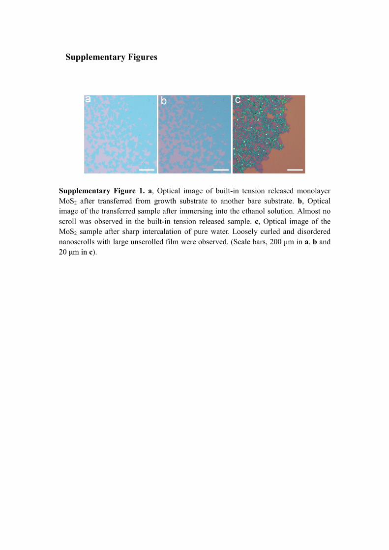
Supplementary Figure 1. a, Optical image of built-in tension released monolayer MoS2 after transferred from growth substrate to another bare substrate. b, Optical image of the transferred sample after immersing into the ethanol solution. Almost no scroll was observed in the built-in tension released sample. c, Optical image of the MoS2 sample after sharp intercalation of pure water. Loosely curled and disordered nanoscrolls with large unscrolled film were observed. (Scale bars, 200 μm in a, b and 20 μm in c).
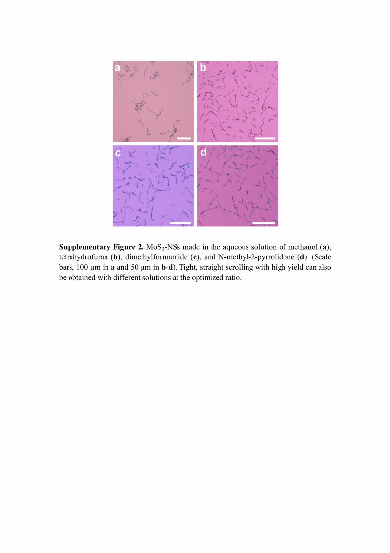
Supplementary Figure 2. MoS2-NSs made in the aqueous solution of methanol (a), tetrahydrofuran (b), dimethylformamide (c), and N-methyl-2-pyrrolidone (d). (Scale bars, 100 μm in a and 50 μm in b-d). Tight, straight scrolling with high yield can also be obtained with different solutions at the optimized ratio.
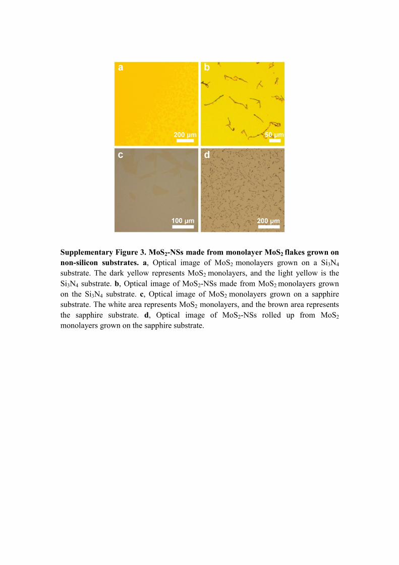
Supplementary Figure 3. MoS2-NSs made from monolayer MoS2 flakes grown on non-silicon substrates. a, Optical image of MoS2 monolayers grown on a Si3N4 substrate. The dark yellow represents MoS2 monolayers, and the light yellow is the Si3N4 substrate. b, Optical image of MoS2-NSs made from MoS2 monolayers grown on the Si3N4 substrate. c, Optical image of MoS2 monolayers grown on a sapphire substrate. The white area represents MoS2 monolayers, and the brown area represents the sapphire substrate. d, Optical image of MoS2-NSs rolled up from MoS2 monolayers grown on the sapphire substrate.
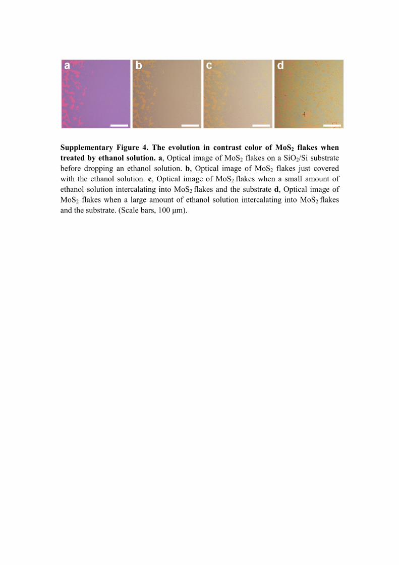
Supplementary Figure 4. The evolution in contrast color of MoS2 flakes when treated by ethanol solution. a, Optical image of MoS2 flakes on a SiO2/Si substrate before dropping an ethanol solution. b, Optical image of MoS2 flakes just covered with the ethanol solution. c, Optical image of MoS2 flakes when a small amount of ethanol solution intercalating into MoS2 flakes and the substrate d, Optical image of MoS2 flakes when a large amount of ethanol solution intercalating into MoS2 flakes and the substrate. (Scale bars, 100 μm).
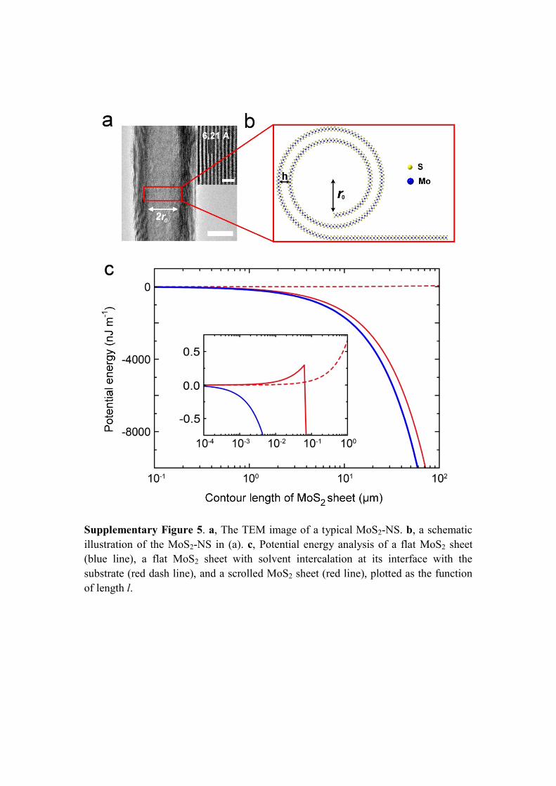
Supplementary Figure 5. a, The TEM image of a typical MoS2-NS. b, a schematic illustration of the MoS2-NS in (a). c, Potential energy analysis of a flat MoS2 sheet (blue line), a flat MoS2 sheet with solvent intercalation at its interface with the substrate (red dash line), and a scrolled MoS2 sheet (red line), plotted as the function of length l.
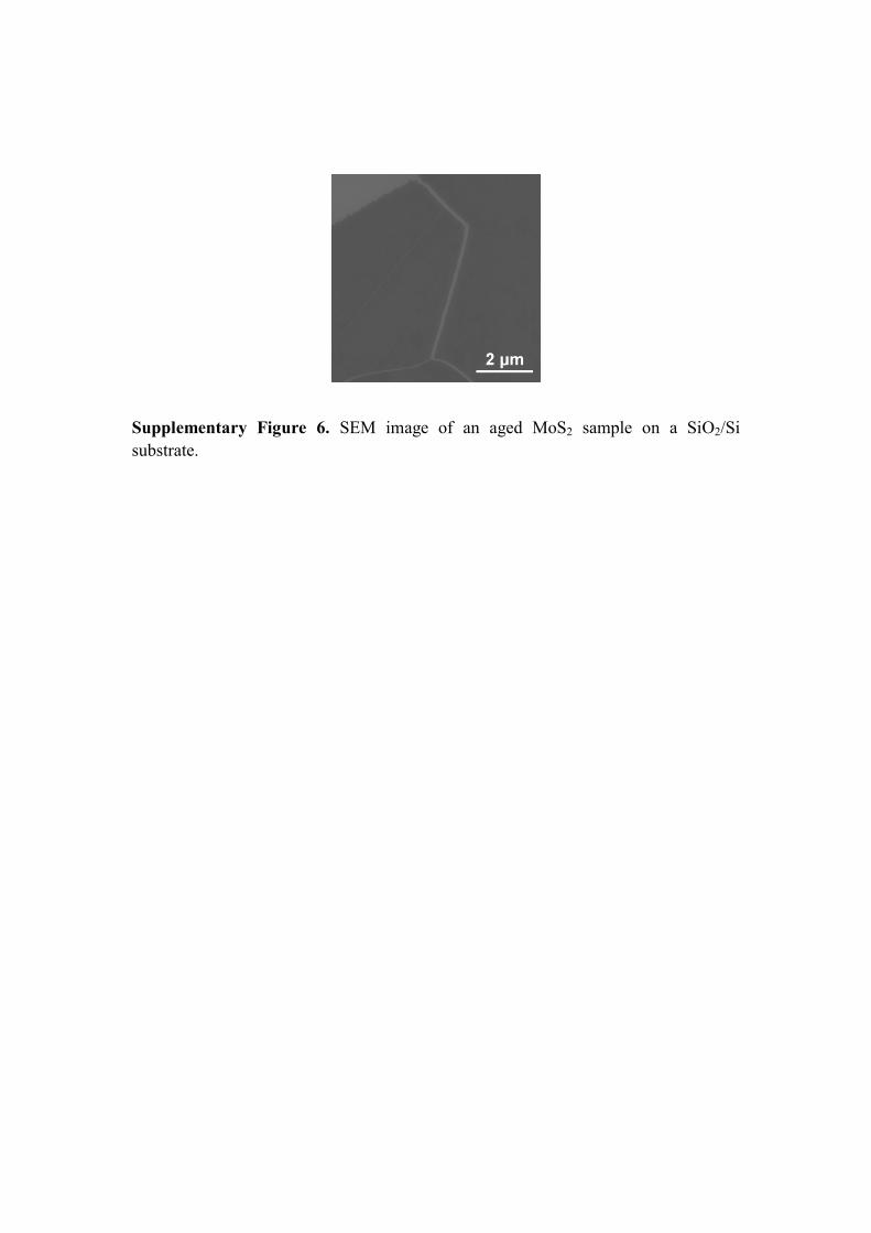
Supplementary Figure 6. SEM image of an aged MoS2 sample on a SiO2/Si substrate.
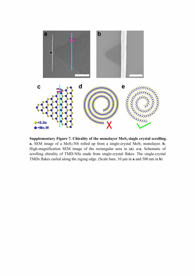
Supplementary Figure 7. Chirality of the monolayer MoS2 single crystal scrolling. a, SEM image of a MoS2-NS rolled up from a single-crystal MoS2 monolayer. b, High-magnification SEM image of the rectangular area in (a). c-e, Schematic of scrolling chirality of TMD-NSs made from single-crystal flakes. The single-crystal TMDs flakes curled along the zigzag edge. (Scale bars, 10 μm in a and 500 nm in b)
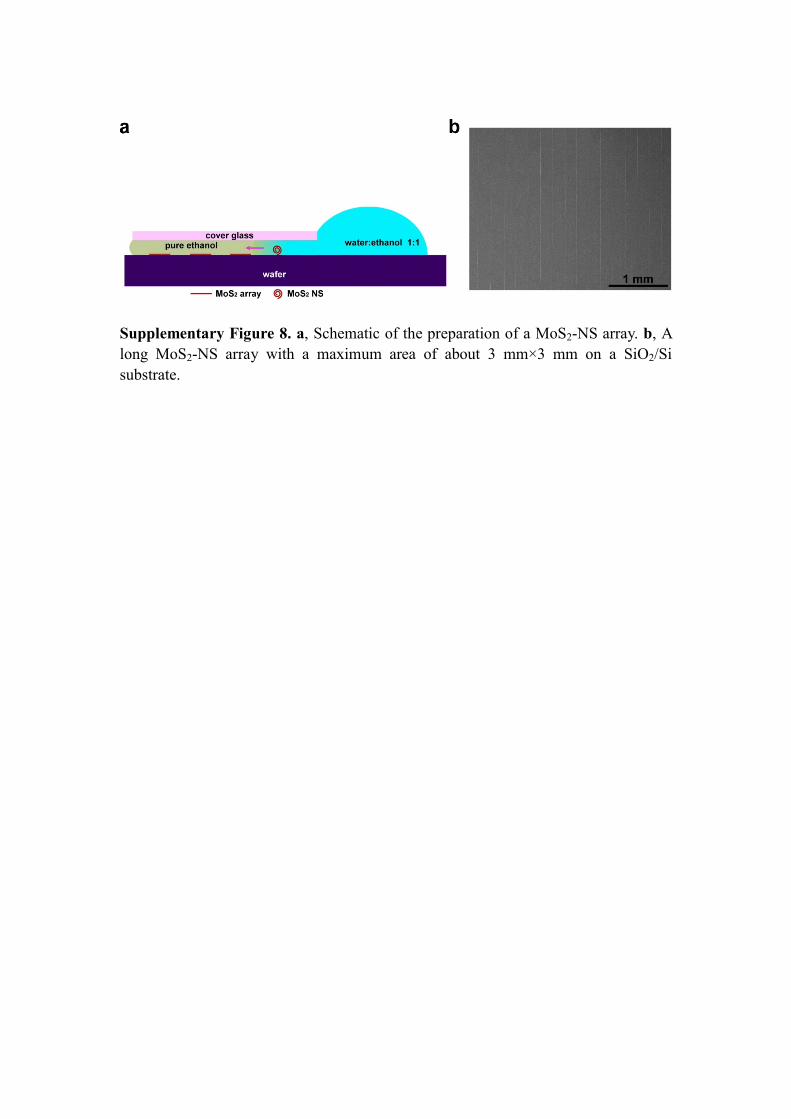
Supplementary Figure 8. a, Schematic of the preparation of a MoS2-NS array. b, A long MoS2-NS array with a maximum area of about 3 mm×3 mm on a SiO2/Si substrate.
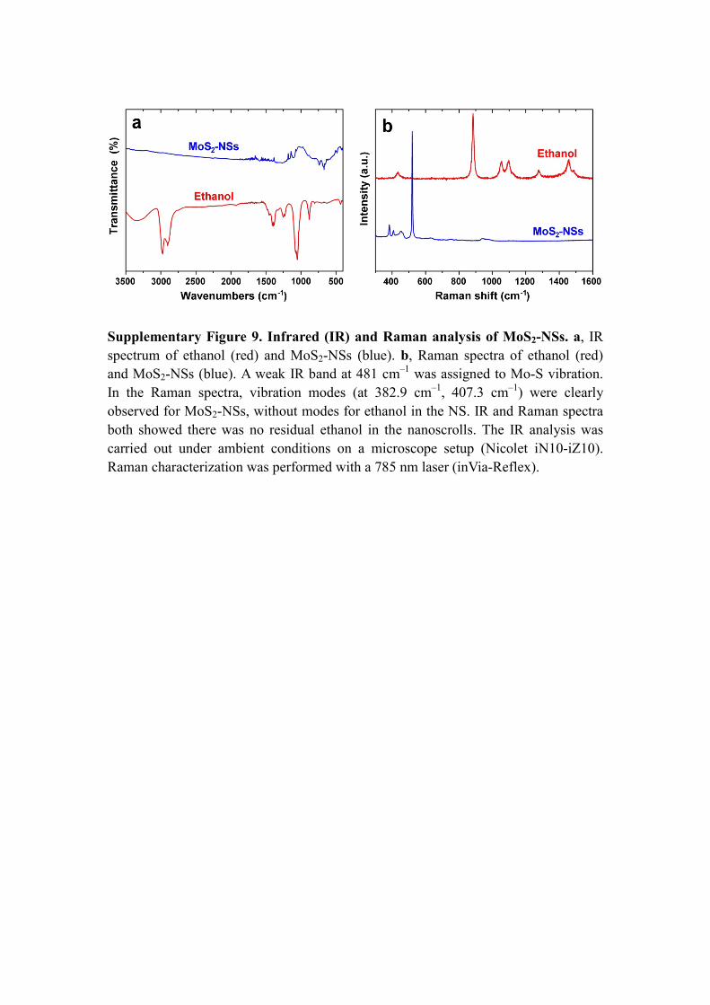
Supplementary Figure 9. Infrared (IR) and Raman analysis of MoS2-NSs. a, IR spectrum of ethanol (red) and MoS2-NSs (blue). b, Raman spectra of ethanol (red) and MoS2-NSs (blue). A weak IR band at 481 cm–1 was assigned to Mo-S vibration. In the Raman spectra, vibration modes (at 382.9 cm–1, 407.3 cm–1) were clearly observed for MoS2-NSs, without modes for ethanol in the NS. IR and Raman spectra both showed there was no residual ethanol in the nanoscrolls. The IR analysis was carried out under ambient conditions on a microscope setup (Nicolet iN10-iZ10). Raman characterization was performed with a 785 nm laser (inVia-Reflex).
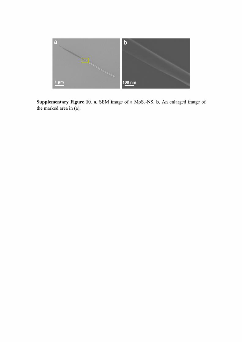
Supplementary Figure 10. a, SEM image of a MoS2-NS. b, An enlarged image of the marked area in (a).
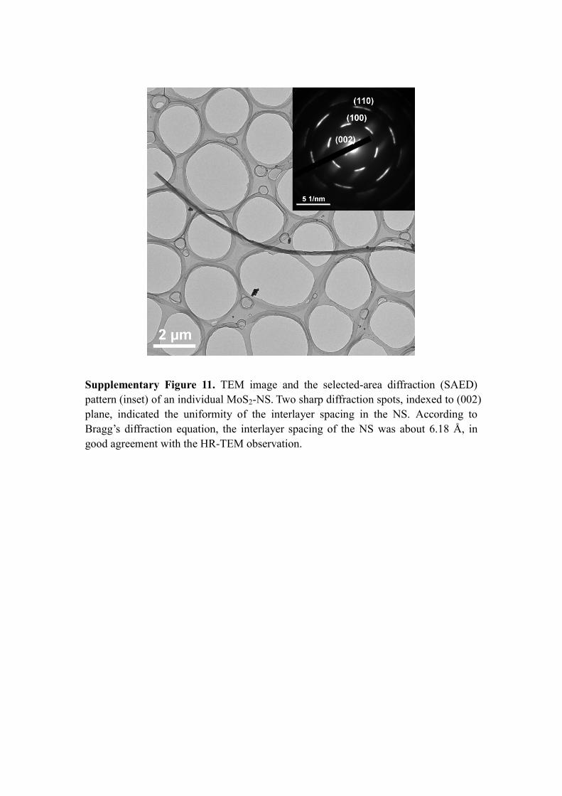
Supplementary Figure 11. TEM image and the selected-area diffraction (SAED) pattern (inset) of an individual MoS2-NS. Two sharp diffraction spots, indexed to (002) plane, indicated the uniformity of the interlayer spacing in the NS. According to Bragg’s diffraction equation, the interlayer spacing of the NS was about 6.18 Å, in good agreement with the HR-TEM observation.
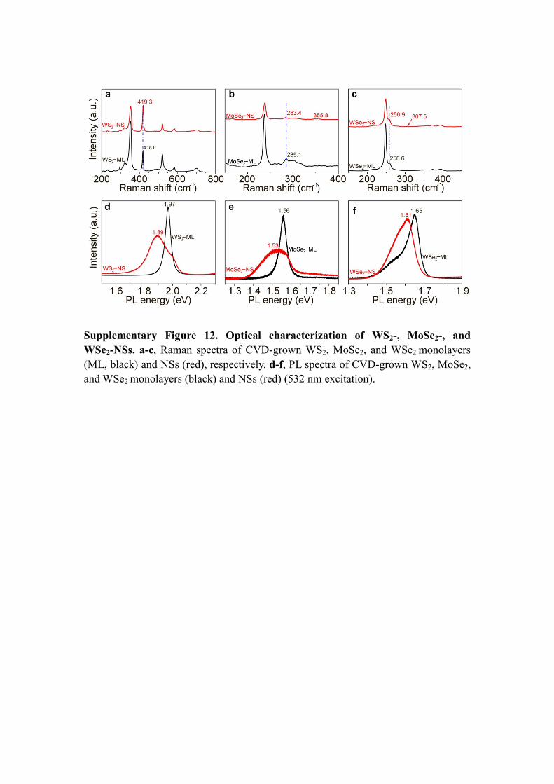
Supplementary Figure 12. Optical characterization of WS2-, MoSe2-, and WSe2-NSs. a-c, Raman spectra of CVD-grown WS2, MoSe2, and WSe2 monolayers (ML, black) and NSs (red), respectively. d-f, PL spectra of CVD-grown WS2, MoSe2, and WSe2 monolayers (black) and NSs (red) (532 nm excitation).
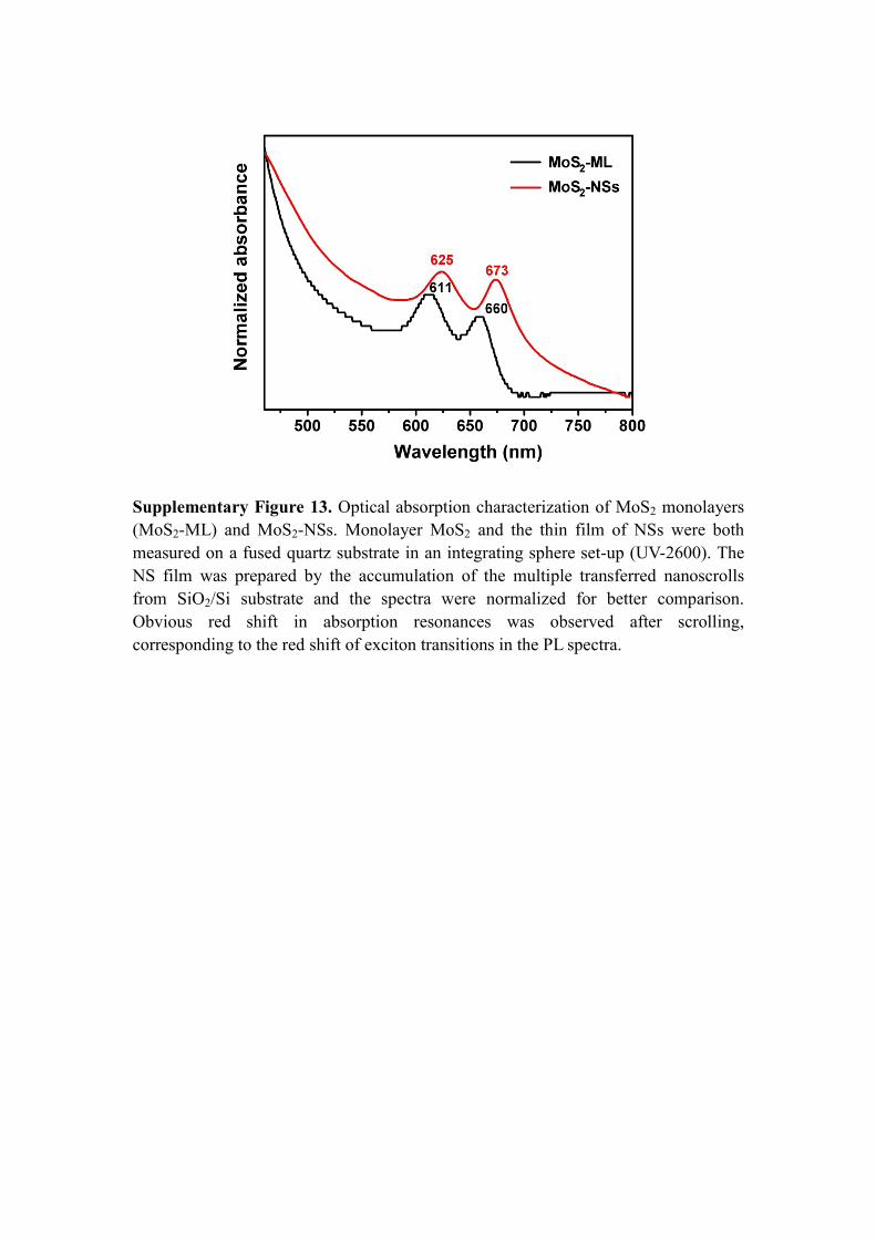
Supplementary Figure 13. Optical absorption characterization of MoS2 monolayers (MoS2-ML) and MoS2-NSs. Monolayer MoS2 and the thin film of NSs were both measured on a fused quartz substrate in an integrating sphere set-up (UV-2600). The NS film was prepared by the accumulation of the multiple transferred nanoscrolls from SiO2/Si substrate and the spectra were normalized for better comparison. Obvious red shift in absorption resonances was observed after scrolling, corresponding to the red shift of exciton transitions in the PL spectra.
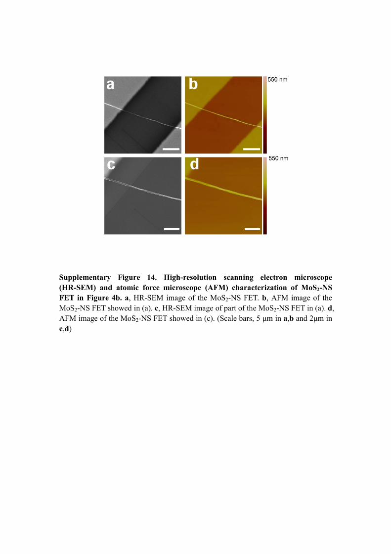
Supplementary Figure 14. High-resolution scanning electron microscope (HR-SEM) and atomic force microscope (AFM) characterization of MoS2-NS FET in Figure 4b. a, HR-SEM image of the MoS2-NS FET. b, AFM image of the MoS2-NS FET showed in (a). c, HR-SEM image of part of the MoS2-NS FET in (a). d, AFM image of the MoS2-NS FET showed in (c). (Scale bars, 5 μm in a,b and 2μm in c,d)
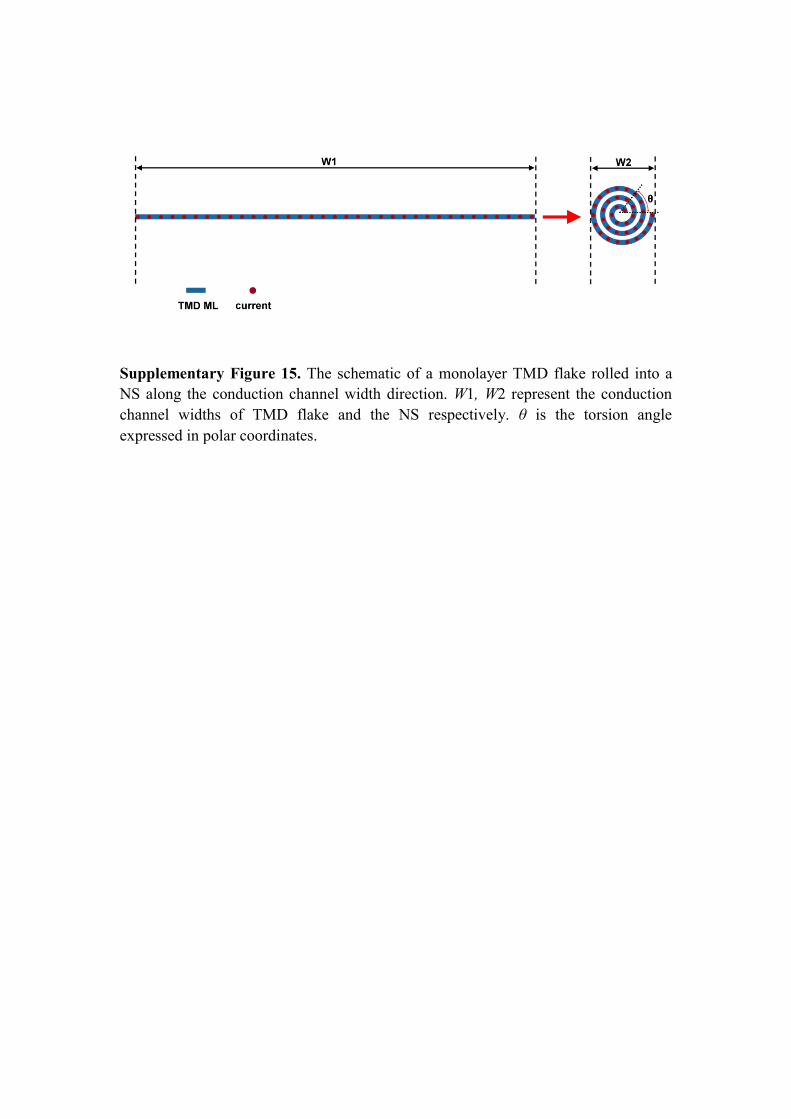
Supplementary Figure 15. The schematic of a monolayer TMD flake rolled into a NS along the conduction channel width direction. W1, W2 represent the conduction channel widths of TMD flake and the NS respectively. θ is the torsion angle expressed in polar coordinates.
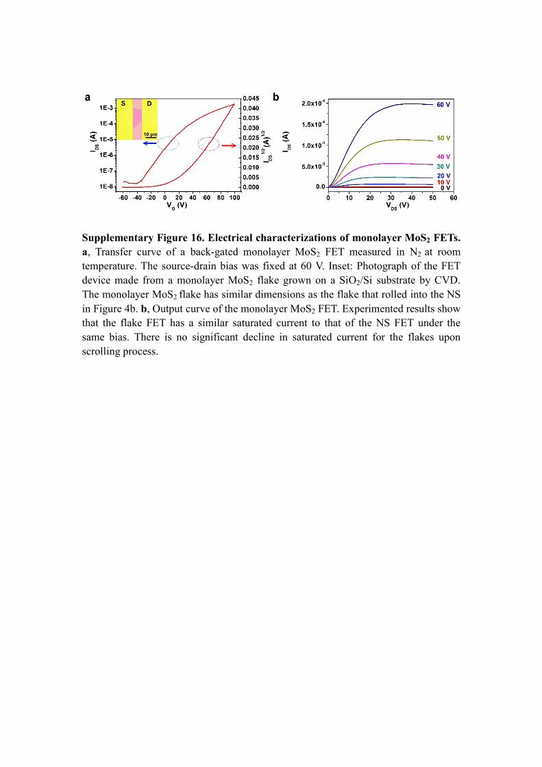
Supplementary Figure 16. Electrical characterizations of monolayer MoS2 FETs. a, Transfer curve of a back-gated monolayer MoS2 FET measured in N2 at room temperature. The source-drain bias was fixed at 60 V. Inset: Photograph of the FET device made from a monolayer MoS2 flake grown on a SiO2/Si substrate by CVD. The monolayer MoS2 flake has similar dimensions as the flake that rolled into the NS in Figure 4b. b, Output curve of the monolayer MoS2 FET. Experimented results show that the flake FET has a similar saturated current to that of the NS FET under the same bias. There is no significant decline in saturated current for the flakes upon scrolling process.
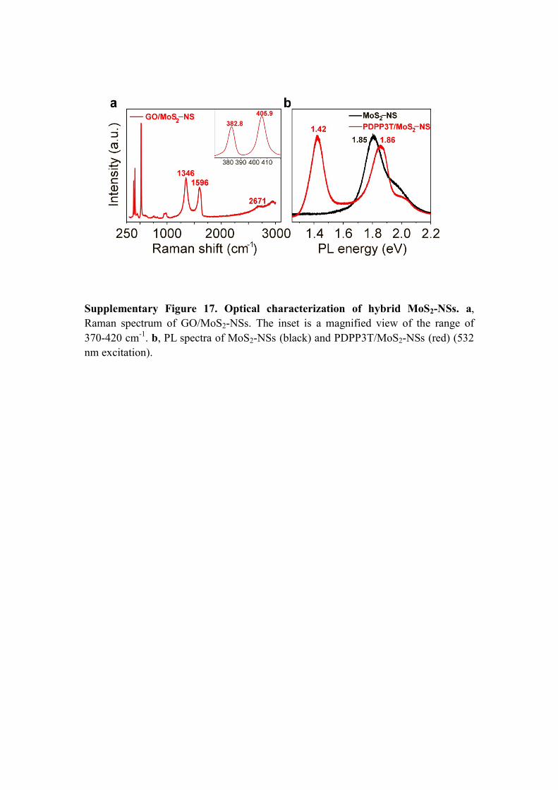
Supplementary Figure 17. Optical characterization of hybrid MoS2-NSs. a, Raman spectrum of GO/MoS2-NSs. The inset is a magnified view of the range of 370-420 cm-1. b, PL spectra of MoS2-NSs (black) and PDPP3T/MoS2-NSs (red) (532 nm excitation).
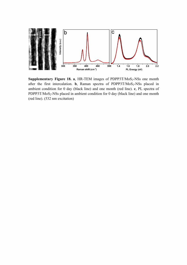
Supplementary Figure 18. a, HR-TEM images of PDPP3T/MoS2-NSs one month after the first intercalation. b, Raman spectra of PDPP3T/MoS2-NSs placed in ambient condition for 0 day (black line) and one month (red line). c, PL spectra of PDPP3T/MoS2-NSs placed in ambient condition for 0 day (black line) and one month (red line). (532 nm excitation)
Supplementary Notes
Supplementary Note 1. The role of immersing solution in CVD-based TMD flake scrolling
To clarify the role of the immersing solution in TMD flake scrolling, an analog experiment was carried out. CVD-grown MoS2 flakes were transferred from growth substrate to another bare SiO2/Si substrate with a polymer-based method. In this process, the built-in tension in the flakes can be released because of the elastic polymer support [1]. Then the transferred sample was immersed into the ethanol solution for 30 minutes. Almost no scrolls were observed in the transferred sample after the procedures above, as shown in Supplementary Fig. 1a and b. The result indicated that the tension to scroll the flake was not induced by the immersing solution. It was observed that the immersing solution here was to intercalate into the flake and the substrate, thereby weakening the adhesion between them. This was crucial for built-in tension to initiate the flake scrolling, as analyzed in theory section (Supplementary Note 2). The existence of water was found to be indispensable to the intercalation. A strong interaction of hydrogen bond can be formed between water and the growth substrate (SiO2/Si, Si3N4 or sapphire), which is stronger than the Van der Waals' force between TMD flakes (hydrophobic) and the substrate. Thus after being dropped on the sample, the water tends to substitute the flakes to contact with the substrate, leading to the intercalation between flakes and the substrate. Instantaneous intercalation happened to the samples when only water used. But the sharp intercalation often caused large pieces of TMD film peeled off together from the
substrate and floated in the water, giving rise to loosely curled, disordered nanoscrolls with large film unscrolled (Supplementary Fig. 1c). A moderate intercalation speed is required for the formation of high-quality nanoscrolls. Under a low intercalation speed, the substrate can act as a template to enable the flake to scroll straightly and tightly. Mixing water with water-soluble organic solvents, such as ethanol, methanol and dimethylformamide, was observed to slow down the intercalation. When only pure organic solvent was used, the intercalation proceeded quite slowly, and even cannot be observed. Optimizing the ratio of water and organic solvents in solution, high-quality scrolling of TMD flakes can be achieved. With the same concentration of aqueous solution, the scrolling speed slightly increased with the polarity of the organic solvent. High-quality scrolling can also be obtained with different solutions at the optimized ratio, as shown in Supplementary Fig. 2.
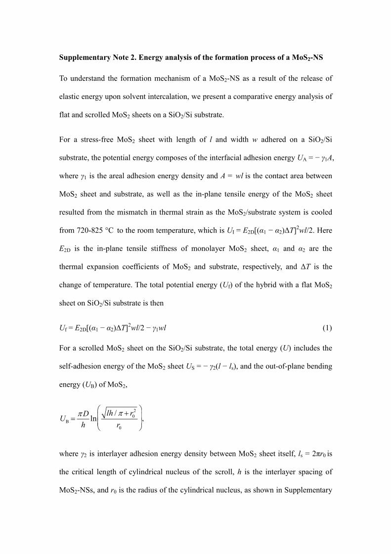
Supplementary Note 2. Energy analysis of the formation process of a MoS2-NS To understand the formation mechanism of a MoS2-NS as a result of the release of elastic energy upon solvent intercalation, we present a comparative energy analysis of flat and scrolled MoS2 sheets on a SiO2/Si substrate.
For a stress-free MoS2 sheet with length of l and width w adhered on a SiO2/Si substrate, the potential energy composes of the interfacial adhesion energy UA = − γ1A, where γ1 is the areal adhesion energy density and A = wl is the contact area between MoS2 sheet and substrate, as well as the in-plane tensile energy of the MoS2 sheet resulted from the mismatch in thermal strain as the MoS2/substrate system is cooled from 720-825 °C to the room temperature, which is UI = E2D[(α1 − α2)ΔT]2wl/2. Here E2D is the in-plane tensile stiffness of monolayer MoS2 sheet, α1 and α2 are the thermal expansion coefficients of MoS2 and substrate, respectively, and ΔT is the change of temperature. The total potential energy (Uf) of the hybrid with a flat MoS2 sheet on SiO2/Si substrate is then
Uf = E2D[(α1 − α2)ΔT]2wl/2 − γ1wl (1) For a scrolled MoS2 sheet on the SiO2/Si substrate, the total energy (U) includes the self-adhesion energy of the MoS2 sheet US = − γ2(l − ls), and the out-of-plane bending energy (UB) of MoS2,
UB = pDh ln lh / p + r0
2
r0
æèçç
öø÷÷,
where γ2 is interlayer adhesion energy density between MoS2 sheet itself, ls = 2πr0 is the critical length of cylindrical nucleus of the scroll, h is the interlayer spacing of MoS2-NSs, and r0 is the radius of the cylindrical nucleus, as shown in Supplementary
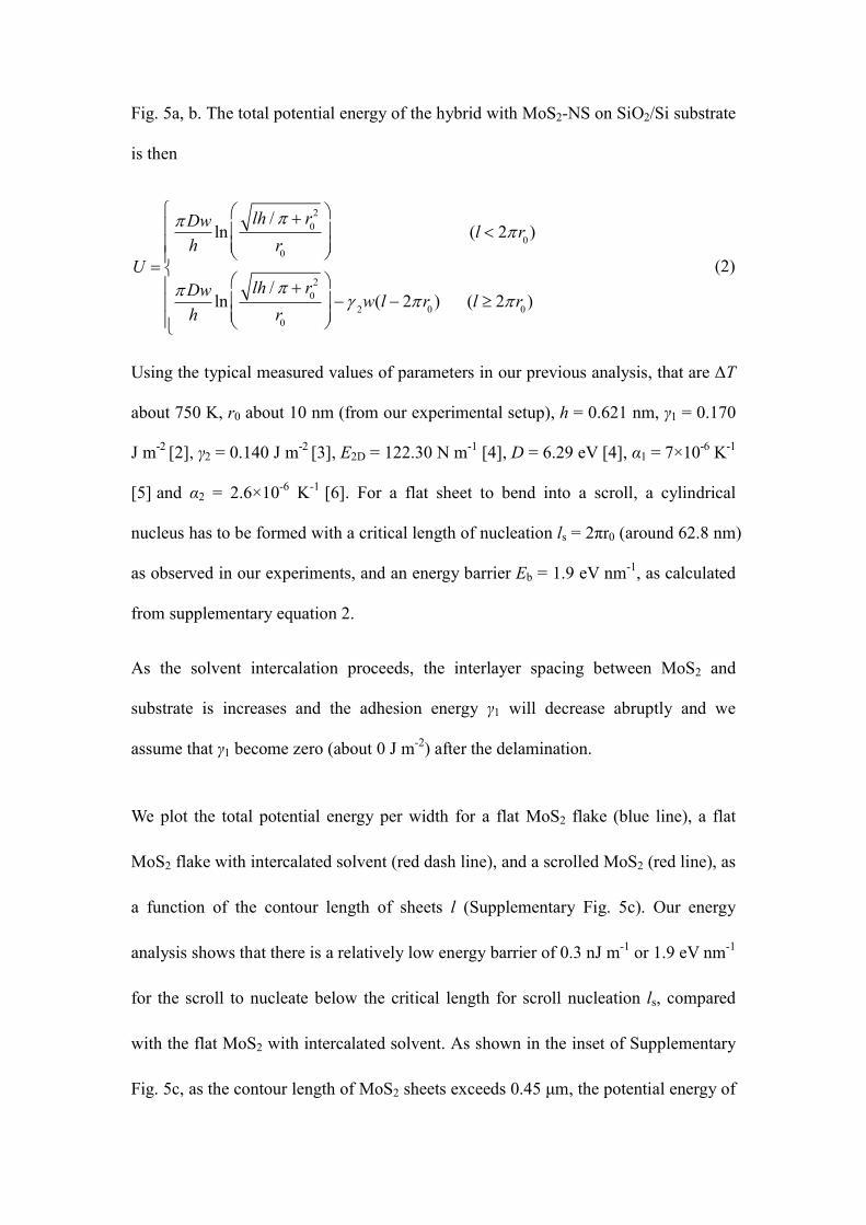
Fig. 5a, b. The total potential energy of the hybrid with MoS2-NS on SiO2/Si substrate is then
U =pDw
h ln lh /p + r02
r0
æèçç
öø÷÷ (l < 2pr0 )
pDwh ln lh /p + r0
2
r0
æèçç
öø÷÷ -g 2w(l - 2p r0 ) (l ³ 2pr0 )
ì
íïïï
îïïï
(2)
Using the typical measured values of parameters in our previous analysis, that are ΔT about 750 K, r0 about 10 nm (from our experimental setup), h = 0.621 nm, γ1 = 0.170 J m-2 [2], γ2 = 0.140 J m-2 [3], E2D = 122.30 N m-1 [4], D = 6.29 eV [4], α1 = 7×10⁻⁶ K-1 [5] and α2 = 2.6×10⁻⁶ K-1 [6]. For a flat sheet to bend into a scroll, a cylindrical nucleus has to be formed with a critical length of nucleation ls = 2πr0 (around 62.8 nm) as observed in our experiments, and an energy barrier Eb = 1.9 eV nm-1, as calculated from supplementary equation 2.
As the solvent intercalation proceeds, the interlayer spacing between MoS2 and substrate is increases and the adhesion energy γ1 will decrease abruptly and we assume that γ1 become zero (about 0 J m-2) after the delamination.
We plot the total potential energy per width for a flat MoS2 flake (blue line), a flat MoS2 flake with intercalated solvent (red dash line), and a scrolled MoS2 (red line), as a function of the contour length of sheets l (Supplementary Fig. 5c). Our energy analysis shows that there is a relatively low energy barrier of 0.3 nJ m-1 or 1.9 eV nm-1 for the scroll to nucleate below the critical length for scroll nucleation ls, compared with the flat MoS2 with intercalated solvent. As shown in the inset of Supplementary Fig. 5c, as the contour length of MoS2 sheets exceeds 0.45 μm, the potential energy of

a flat MoS2 with solvent intercalation (red dash line) is higher than the energy barrier to form scrolled MoS2. This result indicates that the strain energy induced from the thermal mismatch of a flat MoS2 is high enough to activate the formation of scrolls after solvent intercalation and decreasing the adhesion energy with substrate (Supplementary Fig. 5c). It should be remarked here that the conclusion holds on the condition that γ1 becomes lower than γ2 after solvent intercalation.
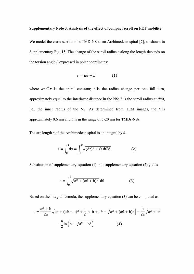
Supplementary Note 3. Analysis of the effect of compact scroll on FET mobility
We model the cross-section of a TMD-NS as an Archimedean spiral [7], as shown in Supplementary Fig. 15. The change of the scroll radius r along the length depends on the torsion angle θ expressed in polar coordinates:
= + (1)
where a=t/2π is the spiral constant; t is the radius change per one full turn, approximately equal to the interlayer distance in the NS; b is the scroll radius at θ=0, i.e., the inner radius of the NS. As determined from TEM images, the t is approximately 0.6 nm and b is in the range of 5-20 nm for TMDs-NSs.
The arc length s of the Archimedean spiral is an integral by θ.
s = ds = (dr) + (r dθ) (2)
Substitution of supplementary equation (1) into supplementary equation (2) yields
s = a + (aθ + b) dθ (3)
Based on the integral formula, the supplementary equation (3) can be computed as
s = aθ + b2a a + (aθ + b) + a
2 ln b + aθ + a + (aθ + b) − b2a a + b
− a2 ln b + a + b (4)
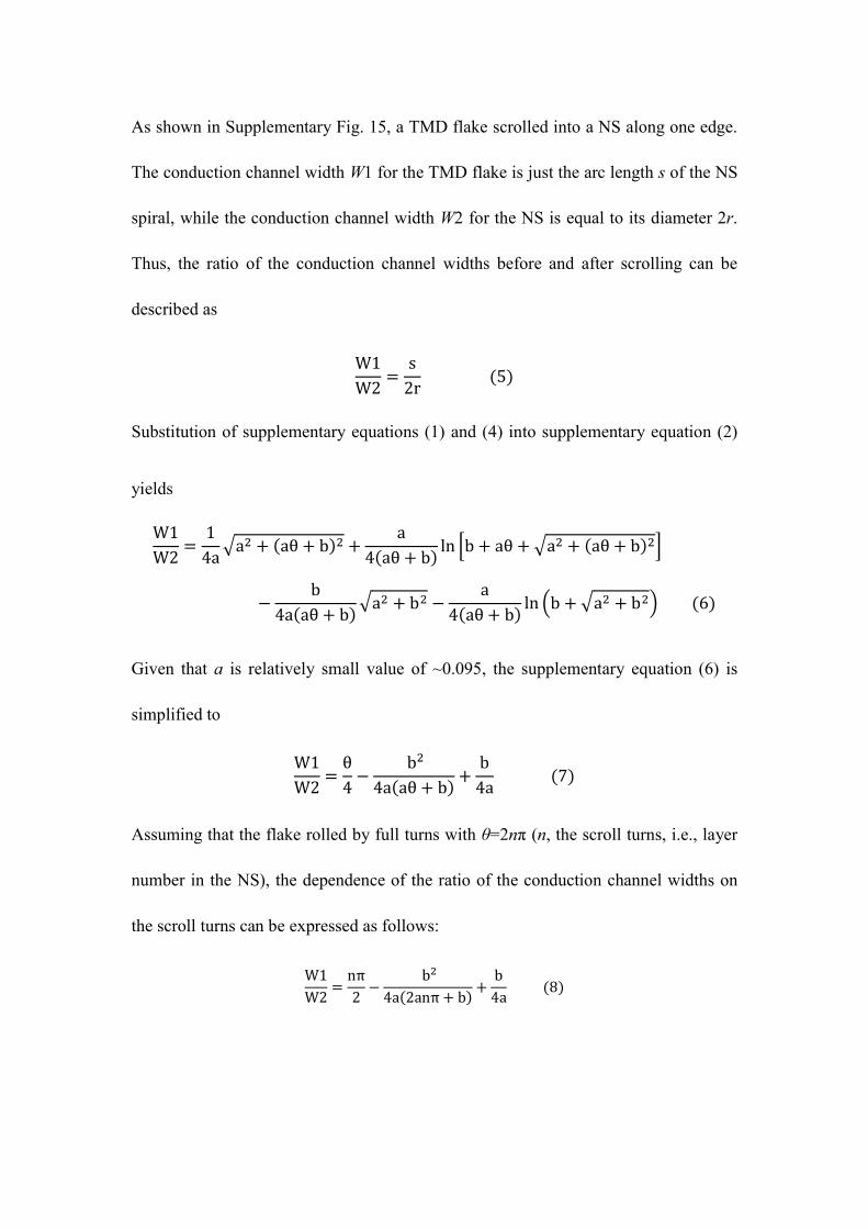
As shown in Supplementary Fig. 15, a TMD flake scrolled into a NS along one edge. The conduction channel width W1 for the TMD flake is just the arc length s of the NS spiral, while the conduction channel width W2 for the NS is equal to its diameter 2r. Thus, the ratio of the conduction channel widths before and after scrolling can be described as
W1W2 = s
2r (5)
Substitution of supplementary equations (1) and (4) into supplementary equation (2)
yields W1W2 = 1
4a a + (aθ + b) + a4(aθ + b) ln b + aθ + a + (aθ + b)
− b4a(aθ + b) a + b − a
4(aθ + b) ln b + a + b (6)
Given that a is relatively small value of ~0.095, the supplementary equation (6) is simplified to
W1W2 = θ
4 − b4a(aθ + b) + b
4a (7)
Assuming that the flake rolled by full turns with θ=2nπ (n, the scroll turns, i.e., layer number in the NS), the dependence of the ratio of the conduction channel widths on the scroll turns can be expressed as follows:
W1W2 = nπ
2 − b4a(2anπ + b) + b
4a (8)
Supplementary References 1. Amani, M. et al. High luminescence efficiency in MoS2 grown by chemical vapor
deposition. ACS Nano 10, 6535−6541 (2016). 2. Deng, S. et al. Adhesion energy of MoS2 thin films on silicon-based substrates
determined via the attributes of a single MoS2 wrinkle. ACS Appl. Mater. Interfaces 9, 7812–7818 (2017).
3. Li, H., Wang, J., Gao, S. et al. Superlubricity between MoS2 monolayers. Adv. Mater. 29, 1701474 (2017).
4. Gao, E., Xu, Z. Thin-shell thickness of two-dimensional materials. J. Appl. Mech. 82, 121012 (2015).
5. Sevik, C. Assessment on lattice thermal properties of two-dimensional honeycomb structures: Graphene, h-BN, h-MoS2, and h-MoSe2. Phys. Rev. B 89, 035422 (2014).
6. Calizo, I., Balandin, A. A., Bao, W., Miao, F., Lau, C. N. Temperature dependence of the Raman spectra of graphene and graphene multilayers. Nano Lett. 7, 2645–2649 (2007)
7. Krasilin, A. A. & Gusarov, V. V. Energy of formation of chrysotile nanotubes. Russ. J. Gen. Chem. 84, 2359–2363 (2014).