
DOD-PP-0484 (1st edition) · DATA SHEET DOD-PP-0484 (1st edition) 4 . 1. OUTLINE . 1.1 STRUCTURE...
28
Document Number: DOD-PP-0484 (1st edition) Published date: February 2008 CP(N) © NEC LCD Technologies, Ltd. 2008 All rights reserved. 1 All information is subject to change without notice. Please confirm the sales representative before starting to design your system. TFT COLOR LCD MODULE NL8048HL11-01B 10.4cm (4.1 Type) WVGA DATA SHEET DOD-PP-0484 (1st edition)
Transcript of DOD-PP-0484 (1st edition) · DATA SHEET DOD-PP-0484 (1st edition) 4 . 1. OUTLINE . 1.1 STRUCTURE...
Document Number: DOD-PP-0484 (1st edition) Published date: February 2008 CP(N)
© NEC LCD Technologies, Ltd. 2008 All rights reserved.
1
All information is subject to change without notice. Please confirm the sales representative before starting to design your system.
TFT COLOR LCD MODULE
NL8048HL11-01B
10.4cm (4.1 Type) WVGA
DATA SHEET DOD-PP-0484 (1st edition)
IMPORTANCE!
Only a copy aiming at perusal of this DATASHEET is permitted. We refuse firmly to reproduce and/or copy this DATASHEET without permission of NEC LCD Technologies, Ltd..

NL8048HL11-01B
DATA SHEET DOD-PP-0484 (1st edition) 2
INTRODUCTION
The Copyright to this document belongs to NEC LCD Technologies, Ltd. (hereinafter called "NEC").
No part of this document will be used, reproduced or copied without prior written consent of NEC.
NEC does and will not assume any liability for infringement of patents, copyrights or other intellectual property rights of any third party arising out of or in connection with application of the products described herein except for that directly attributable to mechanisms and workmanship thereof. No license, express or implied, is granted under any patent, copyright or other intellectual property right of NEC.
Some electronic parts/components would fail or malfunction at a certain rate. In spite of every effort to
enhance reliability of products by NEC, the possibility of failures and malfunction might not be avoided entirely. To prevent the risks of damage to death, human bodily injury or other property arising out thereof or in connection therewith, each customer is required to take sufficient measures in its safety designs and plans including, but not limited to, redundant system, fire-containment and anti-failure. The products are classified into three quality grades: "Standard", "Special", and "Specific" of the
highest grade of a quality assurance program at the choice of a customer. Each quality grade is designed for applications described below. Any customer who intends to use a product for application other than that of Standard quality grade is required to contact an NEC sales representative in advance. The Standard quality grade applies to the products developed, designed and manufactured in
accordance with the NEC standard quality assurance program, which are designed for such application as any failure or malfunction of the products (sets) or parts/components incorporated therein a customer uses are, directly or indirectly, free of any damage to death, human bodily injury or other property, like general electronic devices. Examples: Computers, office automation equipment, communications equipment, test and measurement
equipment, audio and visual equipment, home electronic appliances, machine tools, personal electronic equipment, industrial robots, etc.
The Special quality grade applies to the products developed, designed and manufactured in accordance
with an NEC quality assurance program stricter than the standard one, which are designed for such application as any failure or malfunction of the products (sets) or parts/components incorporated therein a customer uses might directly cause any damage to death, human bodily injury or other property, or such application under more severe condition than that defined in the Standard quality grade without such direct damage. Examples: Control systems for transportation equipment (automobiles, trains, ships, etc.), traffic control
systems, anti-disaster systems, anti-crime systems, medical equipment not specifically designed for life support, safety equipment, etc.
The Specific quality grade applies to the products developed, designed and manufactured in accordance
with the standards or quality assurance program designated by a customer who requires an extremely higher level of reliability and quality for such products. Examples: Military systems, aircraft control equipment, aerospace equipment, nuclear reactor control
systems, medical equipment/devices/systems for life support, etc.
The quality grade of this product is the "Standard" unless otherwise specified in this document.

NL8048HL11-01B
DATA SHEET DOD-PP-0484 (1st edition) 3
CONTENTS
INTRODUCTION ..........................................................................................................................................2
1. OUTLINE....................................................................................................................................................4
1.1 STRUCTURE AND PRINCIPLE...........................................................................................................4 1.2 APPLICATION.......................................................................................................................................4 1.3 FEATURES.............................................................................................................................................4
2. GENERAL SPECIFICATIONS ................................................................................................................5 3. BLOCK DIAGRAM ...................................................................................................................................6 4. DETAILED SPECIFICATIONS ...............................................................................................................8
4.1 MECHANICAL SPECIFICATIONS......................................................................................................8 4.2 ABSOLUTE MAXIMUM RATINGS ....................................................................................................8 4.3 ELECTRICAL CHARACTERISTICS...................................................................................................9 4.4 SETTING OF THE INTERNAL RESISTER.......................................................................................10 4.5 INTERFACE PIN CONNECTIONS ....................................................................................................14 4.6 DISPLAY COLORS AND INPUT DATA SIGNALS ..........................................................................16 4.7 DISPLAY POSITIONS.........................................................................................................................17 4.8 SCANNING DIRECTIONS .................................................................................................................17 4.9 INPUT SIGNAL TIMINGS..................................................................................................................18
4.9.1 RGB interface (Ta= 25°C, VCC= 3.0V) ......................................................................................18 4.9.2 Serial interface (Ta= 25°C, VCC= 3.0V).....................................................................................21
4.10 OPTICAL CHARACTERISTICS ......................................................................................................22 5. RELIABILITY TESTS.............................................................................................................................24 6. PRECAUTIONS .......................................................................................................................................25
6.1 MEANING OF CAUTION SIGNS ......................................................................................................25 6.2 CAUTIONS ..........................................................................................................................................25 6.3 ATTENTIONS ......................................................................................................................................25
6.3.1 Handling of the product ...............................................................................................................25 6.3.2 Environment.................................................................................................................................26 6.3.3 Characteristics..............................................................................................................................26 6.3.4 Other ............................................................................................................................................26
7. OUTLINE DRAWINGS ...........................................................................................................................27 8. RECOMMENDATION DESIGN OF FRONT BEZEL ........................................................................28

NL8048HL11-01B
DATA SHEET DOD-PP-0484 (1st edition) 4
1. OUTLINE
1.1 STRUCTURE AND PRINCIPLE
Color LCD module NL8048HL11-01B is composed of the low temperature poly silicon thin film
transistor liquid crystal display (LTPS TFT LCD) panel structure with driver LSIs for driving the TFT (Thin Film Transistor) array, touch panel (T/P) and a backlight.
The LTPS TFT LCD panel structure is injected liquid crystal material into a narrow gap between the TFT array glass substrate and a color-filter glass substrate.
Color (Red, Green, Blue) data signals from a host system (e.g. signal generator, etc.) are modulated into best form for active matrix system by a controller, and sent to the driver LSIs which drive the individual TFT arrays.
The TFT array as an electro-optical switch regulates the amount of transmitted light from the backlight assembly, when it is controlled by data signals. Color images are created by regulating the amount of transmitted light through the TFT array of red, green and blue dots.
1.2 APPLICATION • PDAs
1.3 FEATURES
• Adoption of VIT (Value integrated TFT) (Transmissive type) • High resolution • High luminance • High contrast • Backlight and touch panel attached • Including LCD controller and power supply • 8-bit digital RGB signals • Compliance with the European RoHS directive (2002/95/EC)

NL8048HL11-01B
DATA SHEET DOD-PP-0484 (1st edition) 5
2. GENERAL SPECIFICATIONS
Display area 88.80 (H) × 53.28 (V) mm
Diagonal size of display 10.4cm (4.1 inches)
Drive system LTPS TFT active matrix
Display color 16,777,216 colors
Pixel 800 (H) × 480 (V) pixels
Pixel arrangement RGB (Red dot, Green dot, Blue dot) vertical stripe
Dot pitch 0.037 (H) × 0.111 (V) mm
Pixel pitch 0.111 (H) × 0.111 (V) mm
Module size 99.6 (H) × 69.5 (V) × 5.0 (D) mm (typ.) [Excluding FPC]
Weight 70g (typ.)
Touch panel surface Clear Touch panel pencil-hardness 3 H (min.) [by JIS K5400]
Designed viewing direction • Viewing direction without image reversal: lower side (6 o'clock) • Viewing direction with contrast peak: up side (12 o'clock)
Luminance At IL= 14mA, with Touch panel 350cd/m2 (typ.)
Contrast ratio At IL= 14mA, with Touch panel 400:1 (typ.)
Response time Ton + Toff (10% ←→ 90%) 25 ms (typ.)
Signal system
8-bit digital signals for data of RGB colors, Dot clock (CLK), Horizontal synchronous signal (HSYNC), Vertical synchronous signal (VSYNC) Serial interface (SPI correspondence ) (/CS, SCL, SI, SO)
Supply voltage VCCIO: 3.0V (typ.) VCC: 3.0V (typ.)
Power consumption LCD panel + Driver: 165mW (typ.) Backlight: 604mW (typ., at IL= 14mA)

NL8048HL11-01B
DATA SHEET DOD-PP-0484 (1st edition) 6
3. BLOCK DIAGRAM
VCOMIN D20 to D27 D10 to D17 D00 to D07 CLK VSYNC HSYNC /RESET /CS SCL SI SO
Driver
Product (LCD panel + Driver + Backlight + Touch panel (T/P))
LCD panel
Backlight
VCC
Ano
de1,
2
Cat
hode
1, 2
Power supply
Input
Backlight
CPU
COM circuit diagram
/RESET/CS
SCLSI
SO(Example of connection)
Touch panel (T/P)
XL
YD
X
R
YU
Touch panel
VCCIOPower supply

NL8048HL11-01B
DATA SHEET DOD-PP-0484 (1st edition) 7
FPC I/F
Reference design of COM circuit
VCOMIN
3.0V
47kΩ
100kΩ
Symbol Pin No.
Driver
2400 lines
LCD panel 480 lines H: 800 × 3 (R, G, B) V: 480
D00 to D07 D10 to D17 D20 to D27 VSYNC HSYNC CLK /RESET /CS SCL SI SO VCOMIN VCCIO VCC GND XL, YD XR, YU ANODE1 CATHODE1 ANODE2 CATHODE2
+3.0V Backlight
Touch panel
+3.0V
11 to 18 19 to 26 27 to 34 8 7 9 6 39 36 37 38 40 41 2, 3, 4 1, 5, 10, 35 42, 47 43, 44, 45, 46 48 49 50 51
NL8048HL11-01B
DATA SHEET DOD-PP-0484 (1st edition) 8
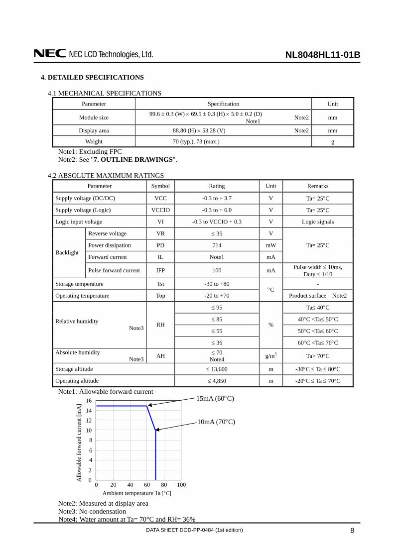
4. DETAILED SPECIFICATIONS
4.1 MECHANICAL SPECIFICATIONS
Parameter Specification Unit
Module size 99.6 ± 0.3 (W) × 69.5 ± 0.3 (H) × 5.0 ± 0.2 (D) Note1 Note2 mm
Display area 88.80 (H) × 53.28 (V) Note2 mm
Weight 70 (typ.), 73 (max.) g
Note1: Excluding FPC Note2: See "7. OUTLINE DRAWINGS".
4.2 ABSOLUTE MAXIMUM RATINGS
Parameter Symbol Rating Unit Remarks
Supply voltage (DC/DC) VCC -0.3 to + 3.7 V Ta= 25°C
Supply voltage (Logic) VCCIO -0.3 to + 6.0 V Ta= 25°C
Logic input voltage VI -0.3 to VCCIO + 0.3 V Logic signals
Reverse voltage VR ≤ 35 V
Power dissipation PD 714 mW
Forward current IL Note1 mA
Ta= 25°C Backlight
Pulse forward current IFP 100 mA Pulse width ≤ 10ms, Duty ≤ 1/10
Storage temperature Tst -30 to +80 -
Operating temperature Top -20 to +70 °C
Product surface Note2
≤ 95 Ta≤ 40°C
≤ 85 40°C <Ta≤ 50°C
≤ 55 50°C <Ta≤ 60°C
Relative humidity Note3 RH
≤ 36
%
60°C <Ta≤ 70°C Absolute humidity
Note3 AH ≤ 70 Note4 g/m3 Ta> 70°C
Storage altitude ≤ 13,600 m -30°C ≤ Ta ≤ 80°C
Operating altitude ≤ 4,850 m -20°C ≤ Ta ≤ 70°C
Note1: Allowable forward current Note2: Measured at display area Note3: No condensation Note4: Water amount at Ta= 70°C and RH= 36%
Ambient temperature Ta [°C]
15mA (60°C)
10mA (70°C)
Allo
wab
le fo
rwar
d cu
rren
t [m
A]
0 2 4 6 8
10 12 14 16
0 20 40 60 80 100
NL8048HL11-01B
DATA SHEET DOD-PP-0484 (1st edition) 9
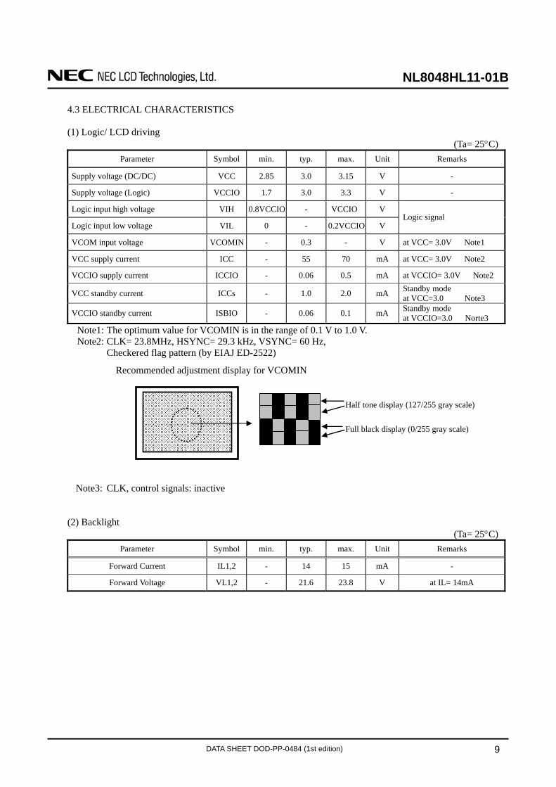
4.3 ELECTRICAL CHARACTERISTICS
(1) Logic/ LCD driving
(Ta= 25°C) Parameter Symbol min. typ. max. Unit Remarks
Supply voltage (DC/DC) VCC 2.85 3.0 3.15 V -
Supply voltage (Logic) VCCIO 1.7 3.0 3.3 V -
Logic input high voltage VIH 0.8VCCIO - VCCIO V
Logic input low voltage VIL 0 - 0.2VCCIO V Logic signal
VCOM input voltage VCOMIN - 0.3 - V at VCC= 3.0V Note1
VCC supply current ICC - 55 70 mA at VCC= 3.0V Note2
VCCIO supply current ICCIO - 0.06 0.5 mA at VCCIO= 3.0V Note2
VCC standby current ICCs - 1.0 2.0 mA Standby mode at VCC=3.0 Note3
VCCIO standby current ISBIO - 0.06 0.1 mA Standby mode at VCCIO=3.0 Norte3
Note1: The optimum value for VCOMIN is in the range of 0.1 V to 1.0 V. Note2: CLK= 23.8MHz, HSYNC= 29.3 kHz, VSYNC= 60 Hz, Checkered flag pattern (by EIAJ ED-2522)
Note3: CLK, control signals: inactive
(2) Backlight (Ta= 25°C)
Parameter Symbol min. typ. max. Unit Remarks
Forward Current IL1,2 - 14 15 mA -
Forward Voltage VL1,2 - 21.6 23.8 V at IL= 14mA
Recommended adjustment display for VCOMIN
Half tone display (127/255 gray scale) Full black display (0/255 gray scale)
NL8048HL11-01B
DATA SHEET DOD-PP-0484 (1st edition) 10
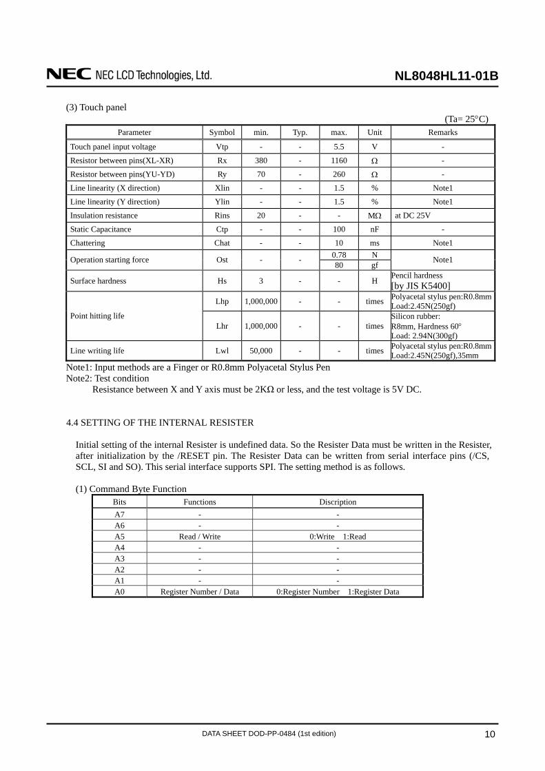
(3) Touch panel
(Ta= 25°C) Parameter Symbol min. Typ. max. Unit Remarks
Touch panel input voltage Vtp - - 5.5 V -
Resistor between pins(XL-XR) Rx 380 - 1160 Ω -
Resistor between pins(YU-YD) Ry 70 - 260 Ω -
Line linearity (X direction) Xlin - - 1.5 % Note1
Line linearity (Y direction) Ylin - - 1.5 % Note1
Insulation resistance Rins 20 - - MΩ at DC 25V
Static Capacitance Ctp - - 100 nF -
Chattering Chat - - 10 ms Note1 0.78 N Operation starting force Ost - - 80 gf
Note1
Surface hardness Hs 3 - - H Pencil hardness [by JIS K5400]
Lhp 1,000,000 - - times Polyacetal stylus pen:R0.8mmLoad:2.45N(250gf)
Point hitting life Lhr 1,000,000 - - times
Silicon rubber: R8mm, Hardness 60° Load: 2.94N(300gf)
Line writing life Lwl 50,000 - - times Polyacetal stylus pen:R0.8mmLoad:2.45N(250gf),35mm
Note1: Input methods are a Finger or R0.8mm Polyacetal Stylus Pen Note2: Test condition
Resistance between X and Y axis must be 2KΩ or less, and the test voltage is 5V DC. 4.4 SETTING OF THE INTERNAL RESISTER
Initial setting of the internal Resister is undefined data. So the Resister Data must be written in the Resister, after initialization by the /RESET pin. The Resister Data can be written from serial interface pins (/CS, SCL, SI and SO). This serial interface supports SPI. The setting method is as follows.
(1) Command Byte Function
Bits Functions Discription A7 - - A6 - - A5 Read / Write 0:Write 1:Read A4 - - A3 - - A2 - - A1 - - A0 Register Number / Data 0:Register Number 1:Register Data

NL8048HL11-01B
DATA SHEET DOD-PP-0484 (1st edition) 11
(2) Timing chart
Note1: During 32-bit transfer of the Resister Data, /CS pin (Pin No.39) must be maintained active. Note2: "X" is set in accordance with the usage conditions. Note3: Data transfer should be performed every 32 bit.
/CS SCL
SI A7 A6 A5 A4 A3 A2 A1 A0 D7 D6 D5 D4 D3 D2 D1 D0
MSB LSB
Command Byte Data Byte - Register Number or Register Data
Ex) When data 55h is written to Register R26 (R1Ah)1st byte 2nd byte
0 1 0 X
/CS SCL
SI X X 0 X X X 0 0 0 0 1 1
MSB LSB Specify to transfer of the resister number value at the next transfer Transfer of the resister number value
0 0
/CS SCL
SI X X 0 X X X X 1 0 1 0 1 1 1
MSB LSB
3rd byte 4th byte
Specify to transfer of the resister data value at the next transfer Transfer of the resister data value
1st byte 2nd byte
0 1 0 X
/CS SCL
SI X X 0 X X X 0 0 0 0 1 1
MSB LSB Specify to transfer of the resister number value at the next transfer Transfer of the resister number value
Ex) When data 55h is read to Register R26 (R1Ah)
/CS SCL
3rd byte 4th byte
Specify to transfer of the resister data value at the next transfer Transfer of the resister data value
SI
0 00 1 0 1 1 1 MSB LSB
X X X X X X X X X 1 X X X X 1 X
SO
NL8048HL11-01B
DATA SHEET DOD-PP-0484 (1st edition) 12
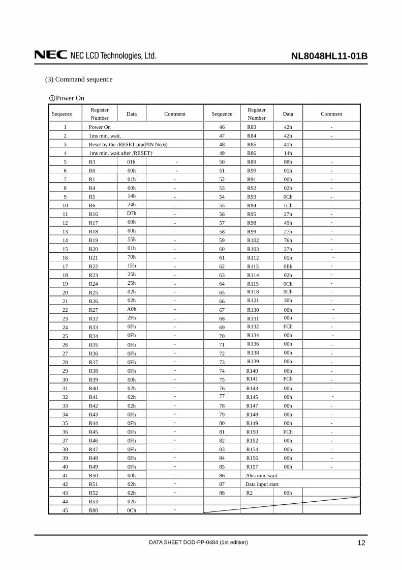
(3) Command sequence
①Power On
Sequence Register Number
Data Comment Sequence Register Number
Data Comment
1 Power On 46 R83 42h - 2 1ms min. wait. 47 R84 42h - 3 Reset by the /RESET pin(PIN No.6) 48 R85 41h 4 1ms min. wait after /RESET↑ 49 R86 14h 5 R3 01h - 50 R89 88h - 6 R0 00h - 51 R90 01h - 7 R1 01h - 52 R91 00h - 8 R4 00h - 53 R92 02h - 9 R5 14h - 54 R93 0Ch -
10 R6 24h - 55 R94 1Ch - 11 R16 D7h - 56 R95 27h - 12 R17 00h - 57 R98 49h -
13 R18 00h - 58 R99 27h -
14 R19 55h - 59 R102 76h -
15 R20 01h - 60 R103 27h - 16 R21 70h - 61 R112 01h -
17 R22 1Eh - 62 R113 0Eh -
18 R23 25h - 63 R114 02h -
19 R24 25h - 64 R115 0Ch -
20 R25 02h - 65 R118 0Ch -
21 R26 02h - 66 R121 30h -
22 R27 A0h - 67 R130 00h -
23 R32 2Fh - 68 R131 00h -
24 R33 0Fh - 69 R132 FCh -
25 R34 0Fh - 70 R134 00h -
26 R35 0Fh - 71 R136 00h - 27 R36 0Fh - 72 R138 00h - 28 R37 0Fh - 73 R139 00h - 29 R38 0Fh - 74 R140 00h - 30 R39 00h - 75 R141 FCh - 31 R40 02h - 76 R143 00h - 32 R41 02h - 77 R145 00h -
33 R42 02h - 78 R147 00h - 34 R43 0Fh - 79 R148 00h - 35 R44 0Fh - 80 R149 00h - 36 R45 0Fh - 81 R150 FCh - 37 R46 0Fh - 82 R152 00h - 38 R47 0Fh - 83 R154 00h - 39 R48 0Fh - 84 R156 00h - 40 R49 0Fh - 85 R157 00h - 41 R50 00h - 86 20us min. wait 42 R51 02h - 87 Data input start 43 R52 02h - 88 R2 00h 44 R53 02h 45 R80 0Ch -

NL8048HL11-01B
DATA SHEET DOD-PP-0484 (1st edition) 13
②Power Off
Sequence Register Number
Data Comment
1 R16 05h - 2 20 us min. wait. 3 R16 01h - 4 20 us min. wait. 5 R16 00h 6 20 us min. wait. 7 R3 01h - 8 Data Off 9 Power Off
③Stand-by
Sequence Register Number
Data Comment
1 R2 01h - 2 40ms min. wait
④Wakeup
Sequence Register Number
Data Comment
1 R2 00h -
⑤Reverse Mode Register
Number Data Comment
01h - Horizontal R1 03h Reverse 30h - Vertical R121 10h Reverse
Note1: Be sure to perform reset by the /RESET pin (Pin No. 6) every power-on Note2: Write the Resister Data every power-on, because the data are not stored in the product. Note3: Due to influence such as static electricity from the outside, data in the register may transform. Data
is recommended to be written in the register regularly.

NL8048HL11-01B
DATA SHEET DOD-PP-0484 (1st edition) 14
4.5 INTERFACE PIN CONNECTIONS
CN1 (FPC) Adaptable socket: FH23-51S-0.3SHW (06) (Hirose Electric Co., Ltd. (HRS))
Pin No. Symbols Functions Pin No. Symbols Functions
1 GND Ground Note1 27 D20 Red data (LSB) 2 VCC 28 D21 Red data 3 VCC 29 D22 Red data 4 VCC
Power supply 30 D23 Red data
5 GND Ground Note1 31 D24 Red data 6 /RESET Reset 32 D25 Red data 7 HSYNC Horizontal synchronous signal 33 D26 Red data 8 VSYNC Vertical synchronous signal 34 D27 Red data (MSB) 9 CLK Dot clock 35 GND Ground Note1 10 GND Ground Note1 36 SCL Serial clock 11 D00 Blue data (LSB) 37 SI Serial input 12 D01 Blue data 38 SO Serial output 13 D02 Blue data 39 /CS Chip selection 14 D03 Blue data 40 VCOMIN COM high voltage input 15 D04 Blue data 41 VCCIO Power supply (Logic) 16 D05 Blue data 42 GND Ground Note1 17 D06 Blue data 43 XL Horizontal terminal (Left side) 18 D07 Blue data (MSB) 44 YD Vertical terminal (Down side) 19 D10 Green data (LSB) 45 XR Horizontal terminal (Right side) 20 D11 Green data 46 YU Vertical terminal (Up side) 21 D12 Green data 47 GND Ground Note1 22 D13 Green data 48 ANODE1 LED1 voltage (Anode) 23 D14 Green data 49 CATHODE1 LED1 voltage (Cathode) 24 D15 Green data 50 ANODE2 LED2 voltage (Anode) 25 D16 Green data 51 CATHODE2 LED2 voltage (Cathode) 26 D17 Green data (MSB) Note1: All GND terminals should be used without any non-connected lines. Note2: Do not fold the FPC. When folding the FPC, pattern disconnection may occur. In case of bending
FPC, the minimum curvature (R) must be more than 1.0 mm.

NL8048HL11-01B
DATA SHEET DOD-PP-0484 (1st edition) 15
Description of terminals
Terminals Description
/RESET When /RESET is L, an internal reset is performed. The reset operation is executed at the /RESET signal level. Be sure to perform reset via this pin at power application.
/CS This pin is used for chip select signals. When /CS= L, the chip is active and can perform data I/O operations including command and data I/O.
SCL This pin is clock input of serial interface. SI This pin is data input of serial interface. SO This pin is data output of serial interface.
VCOMIN This pin is the Common input voltage. The voltage needs to be adjusted. The details are explained the above. See "3 BLOCK DIAGRAM - Reference design of COM circuit".
YU,XR,YD,XL Refer to the below “Circuits of touch panel”. ANODE1,2 CATHODE1,2 Refer to the below “Circuits of backlight”.
XR
YU
XL
XL, YD, XR, YU
YD
Circuits of touch panel Circuits of backlight
Cathode1
Anode1
Cathode2
Anode2
NL8048HL11-01B
DATA SHEET DOD-PP-0484 (1st edition) 16
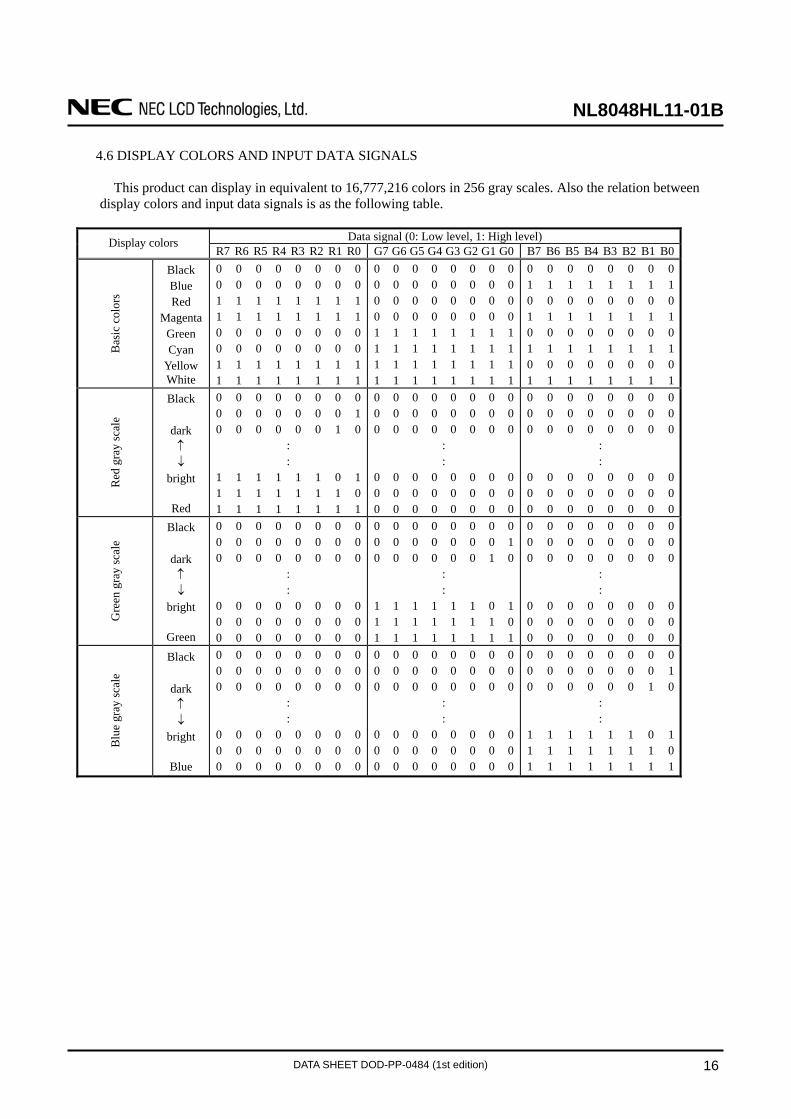
4.6 DISPLAY COLORS AND INPUT DATA SIGNALS
This product can display in equivalent to 16,777,216 colors in 256 gray scales. Also the relation between
display colors and input data signals is as the following table.
Data signal (0: Low level, 1: High level) Display colors R7 R6 R5 R4 R3 R2 R1 R0 G7 G6 G5 G4 G3 G2 G1 G0 B7 B6 B5 B4 B3 B2 B1 B0
Bas
ic c
olor
s
Black Blue Red
Magenta Green Cyan
Yellow White
0 0 0 0 0 0 0 00 0 0 0 0 0 0 01 1 1 1 1 1 1 11 1 1 1 1 1 1 10 0 0 0 0 0 0 00 0 0 0 0 0 0 01 1 1 1 1 1 1 11 1 1 1 1 1 1 1
0 0 0 0 0 0 0 00 0 0 0 0 0 0 00 0 0 0 0 0 0 00 0 0 0 0 0 0 01 1 1 1 1 1 1 11 1 1 1 1 1 1 11 1 1 1 1 1 1 11 1 1 1 1 1 1 1
0 0 0 0 0 0 0 01 1 1 1 1 1 1 10 0 0 0 0 0 0 01 1 1 1 1 1 1 10 0 0 0 0 0 0 01 1 1 1 1 1 1 10 0 0 0 0 0 0 01 1 1 1 1 1 1 1
Red
gra
y sc
ale
Black
dark ↑ ↓
bright
Red
0 0 0 0 0 0 0 00 0 0 0 0 0 0 10 0 0 0 0 0 1 0
: :
1 1 1 1 1 1 0 11 1 1 1 1 1 1 01 1 1 1 1 1 1 1
0 0 0 0 0 0 0 00 0 0 0 0 0 0 00 0 0 0 0 0 0 0
: :
0 0 0 0 0 0 0 00 0 0 0 0 0 0 00 0 0 0 0 0 0 0
0 0 0 0 0 0 0 00 0 0 0 0 0 0 00 0 0 0 0 0 0 0
: :
0 0 0 0 0 0 0 00 0 0 0 0 0 0 00 0 0 0 0 0 0 0
Gre
en g
ray
scal
e
Black
dark ↑ ↓
bright
Green
0 0 0 0 0 0 0 00 0 0 0 0 0 0 00 0 0 0 0 0 0 0
: :
0 0 0 0 0 0 0 00 0 0 0 0 0 0 00 0 0 0 0 0 0 0
0 0 0 0 0 0 0 00 0 0 0 0 0 0 10 0 0 0 0 0 1 0
: :
1 1 1 1 1 1 0 11 1 1 1 1 1 1 01 1 1 1 1 1 1 1
0 0 0 0 0 0 0 00 0 0 0 0 0 0 00 0 0 0 0 0 0 0
: :
0 0 0 0 0 0 0 00 0 0 0 0 0 0 00 0 0 0 0 0 0 0
Blu
e gr
ay sc
ale
Black
dark ↑ ↓
bright
Blue
0 0 0 0 0 0 0 00 0 0 0 0 0 0 00 0 0 0 0 0 0 0
: :
0 0 0 0 0 0 0 00 0 0 0 0 0 0 00 0 0 0 0 0 0 0
0 0 0 0 0 0 0 00 0 0 0 0 0 0 00 0 0 0 0 0 0 0
: :
0 0 0 0 0 0 0 00 0 0 0 0 0 0 00 0 0 0 0 0 0 0
0 0 0 0 0 0 0 00 0 0 0 0 0 0 10 0 0 0 0 0 1 0
: :
1 1 1 1 1 1 0 11 1 1 1 1 1 1 01 1 1 1 1 1 1 1

NL8048HL11-01B
DATA SHEET DOD-PP-0484 (1st edition) 17
4.7 DISPLAY POSITIONS
The following table is the coordinates per pixel (See figure of "4.8 SCANNING DIRECTIONS".).
C (0, 0) C (1, 0)
R G B R G B
C( 0, 0) C( 1, 0) • • • C( X, 0) • • • C(798, 0) C(799, 0)
C( 0, 1) C( 1, 1) • • • C( X, 1) • • • C(798, 1) C(799, 1)
• • •
• • •
• • • •
•
• • •
• • • •
•
• • •
• • • •
• C( 0, Y) C( 1, Y) • • • C( X, Y) • • • C(798, Y) C(799, Y)
• • •
• • •
• • • •
•
• • •
• • • •
•
• • •
• • •
C( 0, 478) C( 1, 478) • • • C( X, 478) • • • C(798, 478) C(799, 478)
C( 0, 479) C( 1, 479) • • • C( X, 479) • • • C(798, 479) C(799, 479)
4.8 SCANNING DIRECTIONS
The following figures are seen from a front view. Also the arrow shows the direction of scan.
Note1: Meaning of C (X, Y) and D (X, Y) C (X, Y): The coordinates of the display position (See "4.7 DISPLAY POSITIONS".) D (X, Y): The data number of input signal for LCD panel
C (0, 0) D (0, 0)
C (0, 479) D (0, 479)
C (799, 479) D (799, 479)
C (799, 0) D (799, 0)
C (0, 0) D (799, 479)
C (0, 479) D (799, 0)
C (799, 479) D (0,0)
C (799, 0) D (0, 479)
Figure1. Normal scan (R1:01h, R121:30h)
Figure2. Reverse scan (R1:03h, R121:10h)

NL8048HL11-01B
DATA SHEET DOD-PP-0484 (1st edition) 18
4.9 INPUT SIGNAL TIMINGS
4.9.1 RGB interface (Ta= 25°C, VCCIO= 3.0V)
(1) Timing characteristics
Parameter Symbol min. typ. max. Unit Remarks
Frequency 1/tc 21.8 23.8 25.7 MHz 42ns (typ.) Duty tcd 0.4 0.5 0.6 - CLK
Rise time, Fall time tcrf - - 2 ns -
Setup time tds 13 - - ns CLK-DATA
Hold time tdh 13 - - ns
DATA (D00-07) (D10-17) (D20-27) Rise time, Fall time tdrf - - 2 ns
-
31.6 34.1 37.2 μs 29.3kHz (typ.) Cycle th
811 CLK
Display period thd 800 CLK
Front-porch thf 6 CLK
Pulse width thp 1 CLK
Back-porch thb 4 CLK
Setup time ths 13 - - ns CLK- HSYNC Hold time thh 13 - - ns
HSYNC
Rise time, Fall time thrf - - 2 ns
-
15.4 16.63 18.2 ms 60Hz (typ.) Cycle tv
488 H
Display period tvd 480 H
Front-porch tvf 3 H
Pulse width tvp 1 H
Back-porch tvb 4 H
VSYNC
Rise time, Fall time tvrf - - 2 ns
-
Note1: Definition of parameters is as follows. tc= 1CLK, tcd= tch/tc, th= 1H
Note2: All parameters should be kept within the specified range.
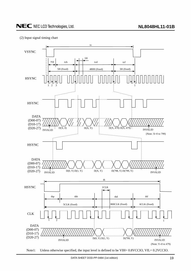
NL8048HL11-01B
DATA SHEET DOD-PP-0484 (1st edition) 19
(2) Input signal timing chart
Note1: Unless otherwise specified, the input level is defined to be VIH= 0.8VCCIO, VIL= 0.2VCCIO.
(Note: X=0 to 799)
1
CLK
HSYNC
HSYNC
HSYNC
HSYNC
VSYNC
2 3
DATA (D00-07) (D10-17) (D20-27)
(Note: Y=0 to 479)
21 1
D(X, 0) D(X, 478) D(X, 479)D(X, Y) INVALID INVALID
1
D(0, Y) D(1, Y) D(X, Y) D(798, Y) D(799, Y)INVALID INVALID
D(0, Y) D(1, Y) D(799, Y)INVALID INVALID
1CLK
5CLK (fixed) 800CLK (fixed)
thp thb thd thf
6CLK (fixed)
5H (fixed) 480H (fixed)
1Htvp tvb tvd tvf
3H (fixed)
DATA (D00-07) (D10-17) (D20-27)
DATA (D00-07) (D10-17) (D20-27)
tv
th

NL8048HL11-01B
DATA SHEET DOD-PP-0484 (1st edition) 20
Note1: Unless otherwise specified, the input level is defined to be VIH= 0.8VCCIO, VIL= 0.2VCCIO.
tdrf
0.8VCCIO 0.2VCCIO
thh
HSYNC
ths
CLK
HSYNC
VSYNC
tvh
tch
INVALID
CLK
DATA (D00-07) (D10-17) (D20-27)
tds tdh
tc
0.8VCCIO 0.2VCCIO
0.8VCCIO 0.2VCCIO
0.8VCCIO 0.2VCCIO
0.8VCCIO 0.2VCCIO
0.8VCCIO 0.2VCCIO
tdrf
thrf thrf
tvrf
tcrf tcrf
NL8048HL11-01B
DATA SHEET DOD-PP-0484 (1st edition) 21
4.9.2 Serial interface (Ta= 25°C, VCCIO= 3.0V)
(1) Timing characteristics
Parameter Symbol Condition min. typ. max. Unit Remarks
Serial clock cycle tSCYC SCL 100 - - ns -
SCL high level pulse width tSHW SCL 50 - - ns -
SCL low level pulse width tSLW SCL 50 - - ns -
/CS rise time, fall time tcsrf /CS - - 2 ns -
SCL rise time, fall time tscrf SCL - - 2 ns -
SI rise time, fall time tsirf SI - - 2 ns -
/CS setup time tCSS /CS 50 - - ns -
/CS hold time tCSH /CS 50 - - ns -
Data setup time tSDS SI 50 - - ns -
Data hold time tSDH SI 50 - - ns -
Reset pulse width tRW /RESET 10 - - μs -
/RESET↑ to /CS time tRCS /RESET↑ to /CS 10 - - μs - Access time tACCS SO - - 150 ns
Output disable time tOHS SO - - 20 ns -
Note1: All parameters should be kept within the specified range.
Note2: Unless otherwise specified, the input level is defined to be VIH= 0.8VCCIO, VIL= 0.2VCCIO.
tsirf
tSDS tSDH
tscrf tscrf
tSHW tSLW
tSCYCtcsrf
tCSH tCSS
tcsrf
tsirf
tRW
0.8VCCIO 0.5VCCIO 0.2VCCIO
SCL
SI 0.8VCCIO 0.5VCCIO 0.2VCCIO
/CS 0.8VCCIO 0.5VCCIO 0.2VCCIO
/RESET 0.8VCCIO 0.5VCCIO 0.2VCCIO
tRCS
tOHS
tACCS
SO 0.8VCCIO 0.5VCCIO 0.2VCCIO
NL8048HL11-01B
DATA SHEET DOD-PP-0484 (1st edition) 22
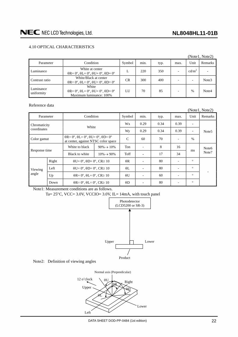
4.10 OPTICAL CHARACTERISTICS
(Note1, Note2)
Parameter Condition Symbol min. typ. max. Unit Remarks
Luminance White at center θR= 0°, θL= 0°, θU= 0°, θD= 0° L 220 350 - cd/m2 -
Contrast ratio White/Black at center θR= 0°, θL= 0°, θU= 0°, θD= 0° CR 300 400 - - Note3
Luminance uniformity
White θR= 0°, θL= 0°, θU= 0°, θD= 0°
Maximum luminance: 100% LU 70 85 - % Note4
Reference data
(Note1, Note2) Parameter Condition Symbol min. typ. max. Unit Remarks
Wx 0.29 0.34 0.39 - Chromaticity coordinates White
Wy 0.29 0.34 0.39 -
Color gamut θR= 0°, θL= 0°, θU= 0°, θD= 0° at center, against NTSC color space C 60 70 - %
Note5
White to black 90%→ 10% Ton - 8 16 Response time
Black to white 10%→ 90% Toff - 17 34 ms Note6
Note7
Right θU= 0°, θD= 0°, CR≥ 10 θR - 80 - °
Left θU= 0°, θD= 0°, CR≥ 10 θL - 80 - °
Up θR= 0°, θL= 0°, CR≥ 10 θU - 60 - °
Viewing angle
Down θR= 0°, θL= 0°, CR≥ 10 θD - 80 - °
-
Note1: Measurement conditions are as follows. Ta= 25°C, VCC= 3.0V, VCCIO= 3.0V, IL= 14mA, with touch panel
Note2: Definition of viewing angles
Photodetector (LCD5200 or SR-3)
Product
Upper Lower
Left
Upper
Lower
Normal axis (Perpendicular)
θR
θL
θD
θU 12 o’clock Right

NL8048HL11-01B
DATA SHEET DOD-PP-0484 (1st edition) 23
Note3: Definition of contrast ratio
The contrast ratio is calculated by using the following formula. Luminance of white screen Luminance of black screen
Note4: Definition of luminance uniformity
Luminance uniformity is calculated by using the following formula.
Note5: The White chromaticity coordinates are deviated by the LED deviation in addition to color filter
deviation.
Note6: Definition of response times
Response time is measured, the luminance changes from "white" to "black", or "black" to "white" on the same screen point, by photo-detector. Ton is the time it takes the luminance change from 90% down to 10%. Also Toff is the time it takes the luminance change from 10% up to 90% (See the following diagram.).
Note7: Product surface temperature: Top= 25°C
100% 90%
10% 0%
Ton Toff
Luminance
White
Black
Minimum luminance from A to I Maximum luminance from A to I
Luminance uniformity (LU) = × 100
1/6 1/2 5/6
1/6
1/2
5/6
A B C
D E F
G H I
Contrast ratio (CR) =
NL8048HL11-01B
DATA SHEET DOD-PP-0484 (1st edition) 24
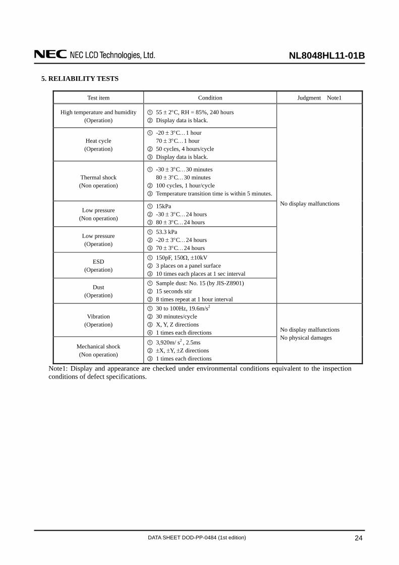
5. RELIABILITY TESTS
Test item Condition Judgment Note1
High temperature and humidity (Operation)
① 55 ± 2°C, RH = 85%, 240 hours ② Display data is black.
Heat cycle (Operation)
① -20 ± 3°C…1 hour 70 ± 3°C…1 hour ② 50 cycles, 4 hours/cycle ③ Display data is black.
Thermal shock (Non operation)
① -30 ± 3°C…30 minutes 80 ± 3°C…30 minutes ② 100 cycles, 1 hour/cycle ③ Temperature transition time is within 5 minutes.
Low pressure (Non operation)
① 15kPa ② -30 ± 3°C…24 hours ③ 80 ± 3°C…24 hours
Low pressure (Operation)
① 53.3 kPa ② -20 ± 3°C…24 hours ③ 70 ± 3°C…24 hours
ESD (Operation)
① 150pF, 150Ω, ±10kV ② 3 places on a panel surface ③ 10 times each places at 1 sec interval
Dust (Operation)
① Sample dust: No. 15 (by JIS-Z8901) ② 15 seconds stir ③ 8 times repeat at 1 hour interval
No display malfunctions
Vibration (Operation)
① 30 to 100Hz, 19.6m/s2 ② 30 minutes/cycle ③ X, Y, Z directions ④ 1 times each directions
Mechanical shock (Non operation)
① 3,920m/ s2 , 2.5ms ② ±X, ±Y, ±Z directions ③ 1 times each directions
No display malfunctions No physical damages
Note1: Display and appearance are checked under environmental conditions equivalent to the inspection conditions of defect specifications.

NL8048HL11-01B
DATA SHEET DOD-PP-0484 (1st edition) 25
6. PRECAUTIONS
6.1 MEANING OF CAUTION SIGNS
The following caution signs have very important meaning. Be sure to read "6.2 CAUTIONS" and "6.3 ATTENTIONS", after understanding these contents!
! This sign has the meaning that customer will be injured by himself or the product will sustain a damage, if customer has wrong operations.
This sign has the meaning that customer will be injured by himself, if customer has wrong operations.
6.2 CAUTIONS
∗ Do not touch the working backlight. There is a danger of burn injury. ∗ Do not shock and press the LCD panel and the backlight! There is a danger of breaking,
because they are made of glass. (Shock: To be not greater 3,920m/s2 and to be not greater 2.5ms)
6.3 ATTENTIONS !
6.3.1 Handling of the product ① Pull out the product from side without FPC and take hold of side with out FPC, when the product
(LCD module) is picked up from the tray. Do not touch the FPC. ② Do not hook nor pull the FPC in order to avoid any damage. ③ When the product is put on the table temporarily, display surface must be placed downward. ④ When handling the product, take the measures of electrostatic discharge with such as earth band,
ionic shower and so on, because the product may be damaged by electrostatic. ⑤ The product must be installed without any stress such as bends or twist. Bends, twist or any stress to
any portion may cause display mura. ⑥ Do not hit or rub the surface of touch panel with hard materials, because it is easily scratched. (Touch panel pencil-hardness: 3H) ⑦ When cleaning the T/P surface, wipe it with a soft dry cloth. ⑧ Do not push nor pull the FPC while the product is working. ⑨ Do not fold the FPC. When folding the FPC, pattern disconnection may occur. In case of bending
FPC, the minimum curvature (R) must be more than 1.0 mm. ⑩ When installing the product, do not contact a conductor such as a metal to the FPC excluding the
terminal area. There is a risk of short circuit which is caused by breakage of insulation layer of the FPC.
⑪ When installing the product, apply the waterproof design to avoid going of water into the product. ⑫ In the external circuit for driving touch panel, take the protection circuit designing to prevent static
electricity. ⑬ Usually liquid crystals don't leak through the breakage of glasses because of the surface tension of
thin layer and the construction of LCD panel. But, if you contact with liquid crystal for the worst, please wash it out with soap.

NL8048HL11-01B
DATA SHEET DOD-PP-0484 (1st edition) 26
6.3.2 Environment
① Do not operate or store in high temperature, high humidity, dewdrop atmosphere or corrosive gases.
Keep the product in packing box with antistatic pouch in room temperature to avoid dusts and sunlight, when storing the product.
② In order to prevent dew condensation occurring by temperature difference, the product packing box should be opened after enough time being left under the environment of an unpacking room. Evaluate the leaving time sufficiently because a situation of dew condensation occurring is changed by the environmental temperature and humidity. (Recommended leaving time: 6 hours or more with packing state)
③ Do not operate in high magnetic field. Circuits may be broken down by it. ④ This product is not designed as radiation hardened.
6.3.3 Characteristics
The following items are neither defects nor failures. ① Response time, luminance and color may be changed by ambient temperature. ② Display mura, flicker, vertical seam or small spot may be observed depending on display patterns. ③ Do not display the fixed pattern for a long time because it may cause image sticking. ④ Optical characteristics may be changed depending on input signal timings. ⑤ Touch panel film has polarizing characteristic. And the polarizer characteristics differ among
products. Therefore, when seeing the displays through the other polarizing material (for example polarizing sunglasses), some displays can not be seen and some displays look different color darker because of polarizer characteristic mismatching between touch panel film and the other polarizing material.
6.3.4 Other
① All GND terminals should be used without any non-connected lines. ② Do not disassemble the product. ③ Pack the product with original shipping package, in order to avoid any damages during transportation,
when returning the product to NEC. ④ When installing the product to the customer equipment, do not apply any stress to the rear side of fhe
product, FPC, A area, Soldering Area and Mounting Area. If not, it may cause display un-uniformity or LCD panel separation or break down of the product.
⑤ The information of China RoHS directive six hazardous substances or elements in this product is as follows.
China RoHS directive six hazardous substances or elements
Lead (Pb)
Mercury (Hg)
Cadmium (Cd)
Hexavalent Chromium
(Cr VI)
Polybrominated Biphenys
(PBB)
Polybrominated Biphenyl Ethers
(PBDE)
⃝ ⃝ ⃝ ⃝ ⃝
Note1: ⃝ : This indicates that the poisonous or harmful material in all the homogeneous materials for this part is equal or below the limitation level of SJ/T11363-2006 standard regulation.
: This indicates that the poisonous or harmful material in all the homogeneous materials for this part is above the limitation level of SJ/T11363-2006 standard regulation.
NL8048HL11-01B
DATA SHEET DOD-PP-0484 (1st edition) 27
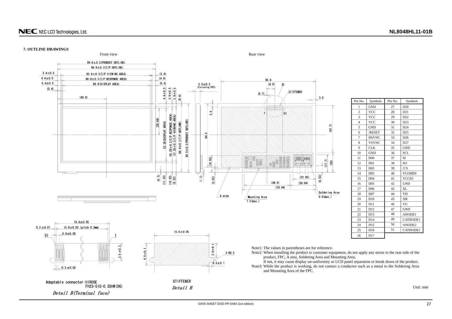
7. OUTLINE DRAWINGS
Unit: mm
Pin No. Symbols Pin No. Symbols
1 GND 27 D20 2 VCC 28 D21 3 VCC 29 D22 4 VCC 30 D23 5 GND 31 D24 6 /RESET 32 D25 7 HSYNC 33 D26 8 VSYNC 34 D27 9 CLK 35 GND 10 GND 36 SCL 11 D00 37 SI 12 D01 38 SO 13 D02 39 /CS 14 D03 40 VCOMIN 15 D04 41 VCCIO 16 D05 42 GND 17 D06 43 XL 18 D07 44 YD 19 D10 45 XR 20 D11 46 YU 21 D12 47 GND 22 D13 48 ANODE1 23 D14 49 CATHODE124 D15 50 ANODE2 25 D16 51 CATHODE226 D17
Note1: The values in parentheses are for reference. Note2: When installing the product to customer equipment, do not apply any stress to the rear side of the
product, FPC, A area, Soldering Area and Mounting Area. If not, it may cause display un-uniformity or LCD panel separation or break down of the product.Note3: While the product is working, do not contact a conductor such as a metal to the Soldering Area
and Mounting Area of the FPC.
Front view Rear view

NL8048HL11-01B
DATA SHEET DOD-PP-0484 (1st edition) 28
8. RECOMMENDATION DESIGN OF FRONT BEZEL
Spacer
Front Bezel
Double-sided adhesive tape
Glass
T/P Response area
Electrode
Touch Panel
PET Film 0.2 - 0.7 mm
Design guidance for the front bezel and the spacer 1. Front Bezel opening design
a. Please place the front bezel opening to maintain the operation by a stylus pen inside the T/P response area. b. Any pressures in the area between T/P response area and T/P viewing area is prohibited. Please use the appropriate material as the front bezel.
2. Spacer design
a. Please put the spacer, a cushion, on the front bezel. Do not use a double-sided adhesive tape because it adheres on the touch panel surface.
b. Please position the spacer over the Spacer area to avoid a “short”.
Front Bezel Opening Design Spacer Design
T/P Viewing area


![S-]Sn D¯ -chv · 2017. 8. 24. · 18 amma skill center telephone: 0484-2532050 mobile: 9744675057 email: ammaskillcenter@gmail.com ... technologies pvt ltd telephone: 0484-4041240](https://static.fdocuments.net/doc/165x107/5fdec14c18fe8d36ac14a58e/s-sn-d-chv-2017-8-24-18-amma-skill-center-telephone-0484-2532050-mobile.jpg)


