Document Copyrightsmanuals.repeater-builder.com/Kenwood/tk/TK-5210 Revised_B51-8703-10.pdf · •...
88
Document Copyrights Copyright 2006 by Kenwood Corporation. All rights reserved. No part of this manual may be reproduced, translated, distributed, or transmitted in any form or by any means, electronic, mechanical, photocopying, recording, or otherwise, for any purpose without the prior written permission of Kenwood. Disclaimer While every precaution has been taken in the preparation of this manual, Kenwood assumes no responsibility for errors or omissions. Neither is any liability assumed for damages resulting from the use of the information contained herein. Kenwood reserves the right to make changes to any products herein at any time for improvement purposes.
Transcript of Document Copyrightsmanuals.repeater-builder.com/Kenwood/tk/TK-5210 Revised_B51-8703-10.pdf · •...

Document CopyrightsCopyright 2006 by Kenwood Corporation. All rights reserved.No part of this manual may be reproduced, translated, distributed, or transmitted in any form or by any means, electronic, mechanical, photocopying, recording, or otherwise, for any purpose without the prior written permission of Kenwood.
DisclaimerWhile every precaution has been taken in the preparation of this manual, Kenwood assumes no responsibility for errors or omissions. Neither is any liability assumed for damages resulting from the use of the information contained herein. Kenwood reserves the right to make changes to any products herein at any time for improvement purposes.

VHF P25 TRANSCEIVER
TK-5210© 2006-9 PRINTED IN JAPANB51-8703-10 (S) 600
SERVICE MANUAL
GENERAL ............................................................... 2
SYSTEM SET-UP ................................................... 2
REALIGNMENT ...................................................... 3
DISASSEMBLY FOR REPAIR .............................. 10
CIRCUIT DESCRIPTION ....................................... 15
TERMINAL FUNCTION ........................................ 21
SEMICONDUCTOR DATA ................................... 25
COMPONENTS DESCRIPTION ........................... 27
PARTS LIST .......................................................... 29
EXPLODED VIEW................................................. 39
PACKING .............................................................. 41
ADJUSTMENT ..................................................... 42
Does not come with antenna. Antenna is available as an option.
PC BOARD
TX-RX UNIT (X57-6820-XX) ........................... 56
SCHEMATIC DIAGRAM....................................... 64
INTERCONNECTION DIAGRAM ......................... 76
BLOCK DIAGRAM ................................................ 77
LEVEL DIAGRAM ................................................. 80
OPTIONAL ACCESSORIES
KNB-31A/32N/33L .......................................... 81
KSC-32 ............................................................. 81
KBP-6 ............................................................... 81
SPECIFICATIONS ..............................BACK COVER
Helical Antenna(KRA-22: Option)
Main cabinet(A02-3875-01)
Knob (16CH)(K29-9323-03)
Knob (Volume)(K29-9322-03)
TK-5210 K TK-5210 K2 TK-5210 K3
CONTENTS
Knob (PTT)(K29-9328-02)
Key top(EMG)(K29-9319-03)
Main cabinet(4key)(A02-3877-11)
Knob (16CH)(K29-9323-03)
Knob (Volume)(K29-9322-03)
Knob (PTT)(K29-9328-02)
Key top(EMG)(K29-9319-03)
Main cabinet(DTMF)(A02-3879-11)
Knob (16CH)(K29-9323-03)
Knob (Volume)(K29-9322-03)
Knob (PTT)(K29-9328-02)
Key top(EMG)(K29-9319-03)
Helical Antenna(KRA-22: Option)
Helical Antenna(KRA-22: Option)
Key top(DTMF)(K29-9321-13)
Key top(4key)(K29-9320-03)
REVISEDThis service manualapplies to products(HARDWARE VER 2.0)with 80600001 orsubsequent serialnumbers.
TK-5210
2
GENERAL / SYSTEM SET-UP
INTRODUCTIONSCOPE OF THIS MANUAL
This manual is intended for use by experienced techniciansfamiliar with similar types of commercial grade communicationsequipment. It contains all required service information for theequipment and is current as of the publication date. Changeswhich may occur after publication are covered by either ServiceBulletins or Manual Revisions. These are issued as required.
ORDERING REPLACEMENT PARTSWhen ordering replacement parts or equipment information, the
full part identification number should be included. This applies to allparts : components, kits, or chassis. If the part number is not known,include the chassis or kit number of which it is a part, and a sufficientdescription of the required component for proper identification.
PERSONAL SAFETYThe following precautions are recommended for personal safety:
• DO NOT transmit until all RF connectors are verified se-cure and any open connectors are properly terminated.
• SHUT OFF and DO NOT operate this equipment near elec-trical blasting caps or in an explosive atmosphere.
• This equipment should be serviced by a qualified technician only.
SERVICEThis transceiver is designed for easy servicing. Refer to
the schematic diagrams, printed circuit board views, andalignment procedures contained within.
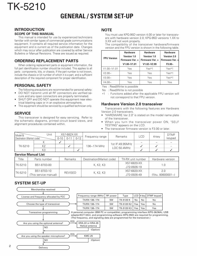
NOTEYou must use KPG-95D version 4.00 or later for transceiv-ers with hardware version 2.0; KPG-95D versions 1.XX to3.XX will not work properly.The compatibility of the transceiver hardware/firmwareversion and the FPU version is shown in the following table.
Hardware Version 2.0 transceiverTransceivers with the following features are Hardware
Version 2.0 transceivers.• "HARDWARE Ver 2.0" is stated on the model name plate
of the transceiver.• When you turn the transceiver power ON, "SELF
TESTING" appears on the LCD.• The transceiver firmware version is F3.00 or later.
SYSTEM SET-UP
Merchandise received
License and frequency allocated by FCC
Choose the type of transceiver
Transceiver programming
Are you using the optional antenna?
Are you using the speaker microphone?
A personal computer (IBM PC or compatible), programming interface (KPG-36/36A), USB adapter(KCT-53U), and programming software (KPG-95D) are required for programming.(The frequency, and signaling data are programmed for the transceiver.)
Frequency range (MHz) RF power Type LCD 4-key DTMF keypad
TX/RX 136~174 5W TK-5120 K No No No
NoTX/RX 136~174 5W TK-5120 K2 Yes Yes
TX/RX 136~174 5W TK-5120 K3 Yes Yes Yes
YESKRA-22 or KRA-26
Helical antennaNO
NO
(Option)
(Option)
YESKMC-25
Delivery
Title Parts number Remarks Destination(Market code) TX-RX unit number Hardware version
TK-5210 B51-8703-00 K, K2, K3X57-6820-XX
1.0J72-0926-19
TK-5210B51-8703-10
REVISED K, K2, K3X57-6820-XX 2.0
(This service manual) J72-0926-49 (S/No. 80600001~)
Service Manual List
Model & Unit X57-682X-XX Frequency range Remarks LCD 4-key
DTMFDestination (Market code) 0-10 0-11 0-12 keypad
K 1st IF:49.95MHz
- - -TK-5210 K2 136~174 MHz
LOC:50.4MHz -
K3
Hardware Hardware Hardware
FPU VersionVersion 1.0 Version 1.0 Version 2.0
Firmware Ver. = Firmware Ver. = Firmware Ver. =
V1.00~V1.01 V1.02~V2.99 F3.00~
V1.00~V1.01 Yes Yes∗1 Yes∗1
V2.00~ Yes Yes Yes∗1
V3.00~ Yes Yes Yes∗1
V4.00~ Yes Yes Yes
Yes : Read/Write is possible No : Read/Write is not possible ∗1 : Functions added after the applicable FPU version will
not correspond to that FPU version.

TK-5210
3
REALIGNMENT
1. Modes 2. How to Enter Each Mode
Mode Operation
User mode Power ON
Panel test mode ∗2 Press and hold the [Side3] and [PTT] keys
while turning the transceiver power ON and
then release the [PTT] key first.
PC mode Received commands from PC
Panel tuning Press the [Side3] key, in Panel test mode
mode ∗2
Firmware Press and hold the [Side3] and [PTT] keys
programming mode while turning the transceiver power ON and
then release the [Side3] key first.
Clone mode ∗2 Press and hold the [Side2] and [PTT] keys
while turning the transceiver power ON and
then release the [Side2] key first.
Self programming Press and hold the [Side2] and [PTT] keys
mode ∗2 while turning the transceiver power ON and
then release the [PTT] key first.
Firmware version Press and hold the [Side3] key while turning
information ∗2 the transceiver power ON.
Clock adjustment Press and hold the [Orange] and [PTT] keys
mode ∗2 while turning the transceiver power ON and
then release the [Orange] key first.
Transceiver Press and hold the [Side1] and [PTT] keys
information mode ∗2 while turning the transceiver power ON and
then release the [PTT] key first.
3. Panel Test Mode (K2 and K3 models only)
Setting method refer to ADJUSTMENT.
4. Panel Tuning Mode (K2 and K3 models only)
Setting method refer to ADJUSTMENT.
User mode
Panel test mode ∗1
Firmware version information ∗1
Panel tuning mode ∗1
Data programming mode
PC test mode PC tuning mode
PC mode
Clone mode ∗1
Firmwareprogramming mode
Clock adjustment mode ∗1
Transceiver information mode ∗1
Self programming mode ∗1
Mode Function
User mode For normal use.
Panel test mode ∗1 Used by the dealer to check the fundamen-
tal characteristics.
Panel tuning mode ∗1 Used by the dealer to tune the transceiver.
PC mode Used for communication between the
transceiver and PC (IBM compatible).
Data programming Used to read and write frequency data and
mode other features to and from the transceiver.
PC test mode Used to check the transceiver using the PC.
This feature is included in the FPU.
See panel tuning.
Firmware Used when changing the main program of
programming mode the flash memory.
Clone mode ∗1 Used to transfer programming data from
one transceiver to another.
Self programming Frequency, signaling and features write to
mode ∗1 the transceiver.
Firmware version Used to confirm the internal firmware
information ∗1 version.
Clock adjustment Used by the dealer to adjust date and time.
mode ∗1
Transceiver Used to confirm the transceiver firmware
information mode ∗1 version.
∗1 : K2 and K3 models only
∗2 : K2 and K3 models only

TK-5210
4
REALIGNMENT
5. PC Mode5-1. Preface
The transceiver is programmed by using a personal com-puter, programming interface (KPG-36/36A), USB adapter(KCT-53U) and programming software (KPG-95D).
The programming software can be used with an IBM PCor compatible. Figure 1 shows the setup of an IBM PC forprogramming.
5-2. Connection procedure1. Connect the transceiver to the computer using the inter-
face cable and USB adapter (When the interface cable isKPG-36A, the KCT-53U can be used.).
Notes:• You must install the KCT-53U driver in the computer to use
the USB adapter (KCT-53U).• When using the USB adapter (KCT-53U) for the first time,
plug the KCT-53U into a USB port on the computer withthe computer power ON.
2. When the POWER switch on, user mode can be enteredimmediately. When PC sends command the transceiverenter PC mode, and “PROGRAM” is displayed on the LCD.When data transmitting from transceiver, the red LED is lights.When data receiving to transceiver, the green LED is lights.
Notes:• The text message are displayed for K2 and K3 models only.• The data stored in the computer must match the "Model
Name and Market Code" when it is written into theEEPROM and flash memory.
5-3. KPG-36/KPG-36A description (PC programming interface cable: Option)
The KPG-36/36A is required to interface the transceiver tothe computer. It has a circuit in its D-sub connector (KPG-36: 25-pin, KPG-36A : 9-pin) case that converts the RS-232Clogic level to the TTL level.
The KPG-36/36A connects the universal connector of thetransceiver to the RS-232C serial port of the computer.
5-4. KCT-53U description (USB adapter : Option)The KCT-53U is a cable which connects the KPG-36A to a
USB port on a computer.When using the KCT-53U, install the supplied CD-ROM
(with driver software) in the computer. The KCT-53U driverruns under Windows 2000 or XP.
5-5. Programming software KPG-95D descriptionThe KPG-95D is the programming software for the trans-
ceiver supplied on a CD-ROM. This software runs under MS-Windows 98, ME, Windows 2000 or XP on an IBM-PC orcompatible machine.
The data can be input to or read from the transceiver andedited on the screen. The programmed or edited data can beprinted out. It is also possible to tune the transceiver.
6. Firmware Programming Mode6-1. Preface
Flash memory is mounted on the transceiver. This allowsthe transceiver to be upgraded when new features are re-leased in the future. (For details on how to obtain the firm-ware, contact Customer Service.)
6-2. Firmware programming operation using
different hardware versions
The firmware that can be written to hardware version 1.0and hardware version 2.0 transceivers is different.
Hardware version 1.0: These transceivers use firmwareversions 1.00 to 2.99. If you attempt touse firmware versions F3.00 or later, a“Check connection” error message willappear on the LCD.
Hardware version 2.0: These transceivers use firmwareversions F3.00 or later. If you attempt touse firmware versions 1.00 to 2.99, a“Check connection” error message willappear on the LCD.
Compatibility of Hardware version and Firmware version
Note:If the firmware is written to the transceiver using acombination that is not applicable, the current transceiverfirmware will not be overwritten.
6-3. Connection procedureConnect the transceiver to the personal computer (IBM
PC or compatible) using the interface cable (KPG-36/36A) andUSB adapter (KCT-53U : when the interface cable is KPG-36A, the KCT-53U can be used.). (Connection is the same asin the PC Mode.)
6-4. Programming1. Start up the firmware programming software (Fpro.exe).2. Set the communications speed (normally, 115200 bps)
and communications port in the configuration item.
Fig. 1
IBM-PC
KPG-95D
KPG-36 or KPG-36A orKPG-36A + KCT-53UIllustration is KPG-36.
KPG-36
Transceiver
PC
D-SUB(25-pin)
Transceiver
PC
KPG-36A
D-SUB(9-pin)
Transceiver
PC
KPG-36A
KCT-53U
USB
Firmware Version
Hardware Version V1.00~V2.99 F3.00~
1.0 Yes No
2.0 No Yes
Yes : Writing is possible No : Writing is not possible
TK-5210
5
REALIGNMENT
3. Set the firmware to be updated by File name item.4. Press and hold the [Side3] and [PTT] keys while turning
the transceiver power ON and then release the [Side3] keyfirst. Then, the orange LED on the transceiver lights andthe baud rate is displayed as follows according to the posi-tion of the Concentric switch.
A: PROGRAM 115200 bpsB: PROGRAM 57600 bpsC: PROGRAM 19200 bps
Since the baud rate is normally set to 115200 bps, changethe Concentric switch to "A".
5. Check the connection between the transceiver and thepersonal computer, and make sure that the transceiver isin the Program mode.
6. Press “write” button in the window. When the trans-ceiver starts to receive data, the [PG] display lights.
7. If writing ends successfully, the checksum is calculatedand a result is displayed.
8. If you want to continue programming other transceivers,repeat steps 4 to 7.
Notes:• This mode cannot be entered if the Firmware Program-
ming mode is set to Disable in the Programming software.• The text message are displayed for K2 and K3 models only.
6-5. Baud rate change1. Change baud rate by changing the Concentric switch posi-
tion. The baud rates are assigned to positions of the Con-centric switch as follows:
A: PROGRAM 115200 bps (The LED lights orange)B: PROGRAM 57600 bps (The LED blinks orange)C: PROGRAM 19200 bps (The LED blinks green)
2. If you press the [Side1] switch (top of left side) while thebaud rate (such as “PROGRAM 115200 bps") is displayed,the checksum is calculated, and a result is displayed. Ifyou press the [Side1] switch again while the checksum isdisplayed, the baud rate (such as “PROGRAM 115200bps") is redisplayed.
Notes:• Normally, write in the high-speed mode.• The text message are displayed for K2 and K3 models only.
7. Clone Mode (K2 and K3 models only)Programming data can be transferred from one transceiver
to another by connecting them via their external universal con-nectors. The operation is as follows (the transmit transceiveris the source and the receive transceiver is a target).
The following data cannot be cloned.• Tuning data• Embedded message with password• Model name data• ESN (Electronic Serial Number) data
Key guide on the "INPUT PASSWORD" display.• CNF([A] key): The password confirmation• DEL([B] key): Delete the least digit from the current pass-
word number (Press and hold to delete allpassword numbers)
• SET([D] key): Determine the least digit of the password number
1. Press and hold the [Side2] and [PTT] keys while turning thetransceiver power ON and then release the [Side2] key first.If the Read authorization password is set to the transceiver,the transceiver displays “CLONE LOCK”. If the password isnot set, the transceiver displays “CLONE MODE”.
2. When you enter the correct password, and “CLONE MODE”is displayed, the transceiver can be used as the cloningsource. The following describes how to enter the password.
3.• How to enter the password using the keypad (K3 model only);
If the [D] key is pressed while "CLONE LOCK" is displayed,the Read authorization password input screen (INPUTPASSWORD) is displayed.If one of keys 0 to 9 is pressed while "INPUT PASSWORD"is displayed, the pressed number is displayed on the LCD.Each press of the key shifts the display in order to the left.When you enter the password and press the [A] or []key, “CLONE MODE” is displayed if the entered pass-word is correct. If the password is incorrect, “CLONELOCK” is redisplayed.
• How to enter the password using the [Side2] and[Side3] keys (K2 and K3 models);If the [D] key is pressed while "CLONE LOCK" is displayed,the Read authorization password input screen (INPUTPASSWORD) is displayed.If the [Side2] key or [Side3] key is pressed while "INPUTPASSWORD" is displayed, the number (0 to 9) flashes onthe LCD. When you press the [D] key, the currentlyselected number is determined. If you press the [A] keyafter entering the password in this procedure, “CLONEMODE” is displayed if the entered password is correct. Ifthe password is incorrect, “CLONE LOCK” is redisplayed.
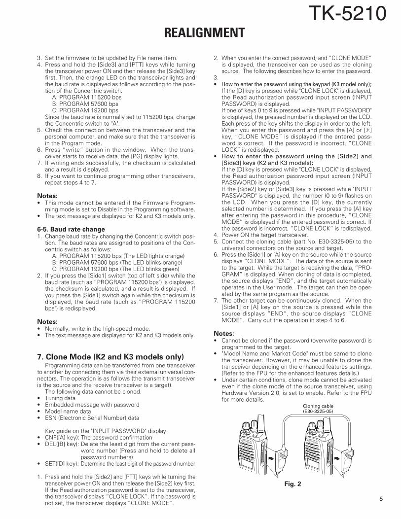
4. Power ON the target transceiver.5. Connect the cloning cable (part No. E30-3325-05) to the
universal connectors on the source and target.6. Press the [Side1] or [A] key on the source while the source
displays “CLONE MODE”. The data of the source is sentto the target. While the target is receiving the data, “PRO-GRAM” is displayed. When cloning of data is completed,the source displays “END”, and the target automaticallyoperates in the User mode. The target can then be oper-ated by the same program as the source.
7. The other target can be continuously cloned. When the[Side1] or [A] key on the source is pressed while thesource displays “END”, the source displays “CLONEMODE”. Carry out the operation in step 4 to 6.
Notes:• Cannot be cloned if the password (overwrite password) is
programmed to the target.• "Model Name and Market Code" must be same to clone
the transceiver. However, it may be unable to clone thetransceiver depending on the enhanced features settings.(Refer to the FPU for the enhanced features details.)
• Under certain conditions, clone mode cannot be activatedeven if the clone mode of the source transceiver, usingHardware Version 2.0, is set to enable. Refer to the FPUfor more details.
Cloning cable(E30-3325-05)
Fig. 2

TK-5210
6
REALIGNMENT
Clone operation depending on hardware and
firmware versionsWhen Clone is executed between transceivers using
different versions of hardware and firmware, the Cloneoperation is as follows.
• Cloning between transceivers using hardware version 1
• Cloning from hardware version 1 to hardware version 2
Note:Under certain conditions, cloning cannot be performedeven if you are using a proper hardware and firmwarecombination. Refer to the FPU for more details.
8. Self Programming Mode(K2 and K3 models only)
Write mode for frequency data and signaling etc. To beused ONLY by the authorized service person maintaining theuser's equipment. After programming, reset the FPU to the"Self- Programming" disabled mode. Transceivers CANNOTbe delivered to the end-user in the self-programming mode.
The following setup items in the channels programmed bythe FPU can be changed using the self-programming mode.The addition of new channel and the deletion of channel thathas already been programmed by the FPU cannot beperformed using the self-programming mode.
• RX frequency• TX frequency• Channel type• TX mode (When the channel type is selected "MIXED".)• Channel spacing• RX signaling• TX signaling• RX NAC• TX NAC• Talkgroup list number
Note:The personality will be also changed when the above-mentioned items is changed. (Refer to the FPU for thepersonality details.)
Key guide on the "INPUT PASSWORD" display.• CNF([A] key): The password confirmation• DEL([B] key): Delete the least digit from the current pass-
word number (Press and hold to delete allpassword numbers)
• SET([D] key): Determine the least digit of the passwordnumber
8-1. Enter to the self programming modePress and hold the [Side2] and [PTT] keys while turning
the transceiver power ON and then release the [PTT] keyfirst. Ignoring whether the Read authorization password isset or not, "INPUT PASSWORD" appears.
If the Read authorization password is not set to the trans-ceiver, "SELF PROG MODE" is displayed on the LCD when the[A] key is pressed while "INPUT PASSWORD" is displayed.
If the password is set to the transceiver, "SELF PROGMODE" is displayed on the LCD when you enter the correctpassword while "INPUT PASSWORD" is displayed.
For the password input method, see "7.Clone Mode”step 3 described on page 5.
Note :This mode (self programming mode) cannot be set whenit has been disabled with the FPU.
8-2. Data WritingIf the [Side3] key is pressed while Zone/Channel mode is
displayed, new data is written into memory. "Writing" is dis-played while the transceiver is writing data.
Source transceiver
(Hardware version 1.0)
Firmware Version
~V1.04
V1.05~V2.99
Target transceiverClone
(Hardware version 1.0)operation
Firmware Version
~V1.04 YesV1.05~V2.99 No
~V1.04 NoV1.05~V2.99 Yes
Yes : Cloning is possible No : Cloning is not possible
→
→
Source transceiver
(Hardware version 1.0)
Firmware Version
~V1.04V1.05~V2.99
Target transceiverClone
(Hardware version 2.0)operation
Firmware Version
F3.00~ NoF3.00~ Yes
Yes : Cloning is possible No : Cloning is not possible
→→
No. Setup item Display Remarks1 Select ZONE [**] -CH *** Zone : 1~50
Zone/Channel ZONE ** -CH [***] CH : 1~2502 RX frequency RX Freq Receive frequency3 TX frequency TX Freq Transmit frequency4 Channel type CH Type ANALOG/P25/MIXED5 TX mode TX Mode ANALOG/P256 Channel spacing CH Space 25.0kHz/12.5kHz (When the Channel type is selected "ANALOG" or "MIXED".)
P25 12.5kHz/12.5kHz (When the Channel type is selected "P25".)7 RX Signaling RX Sig Receive QT/DQT8 TX Signaling TX Sig Transmit QT/DQT9 RX NAC RX NAC *** 000~FFF (Hexadecimal) Note : “F7F” cannot be set.10 TX NAC TX NAC *** 000~FFF (Hexadecimal) Note : “F7E” and “F7F” cannot be set.11 Talkgroup list number TG List No. *** 1~250
The setup items for self programming mode are as follows.

TK-5210
7
Item Zone-Channel RX Frequency TX Frequency Channel Type TX Mode Channel Spacing RX Signaling TX SignalingKey
[A] Go to the next item
Zone/Channel2.5kHz/5kHz/6.25kHz/
QT/DQT(N)/DQT(I)/OFF[B]
switching7.5kHz/1MHz Unused
switchingstep switching
[C]Zone/Channel
1 step downANALOG/P25/MIXED ANALOG/P25 Channel spacing
Signaling downdown switching(Back) switching(Back) switching(Back)
[D]Zone/Channel
1 step upANALOG/P25/MIXED ANALOG/P25 Channel spacing
Signaling upup switching(Forward) switching(Forward) switching(Forward)
[Side3]Data
UnusedON/OFF
Unused1 step/Standard
writing switching switchingKeypad[0]~[9] Unused Go to the direct enter mode Unused
Go to the direct enter mode
(K3 Model only)(After selecting signaling type)
Key operation
Item RX NAC TX NAC TG List No.Key
[A] Go to the next item
[B] Delete the least digit from the current number Unused (Press and hold to delete all numbers.)
[C] Unused TG Listnumber down
[D] Determine the least digit TG Listnumber up
[Side2] Increment a number in the specified digit Unused[Side3] Decrement a number in the specified digit UnusedKeypad Add a digit to the current number
(K3 model only) How to enter the “A” ~ “F” is follows.Unused
A : Press [2] with PTT B : Press [5] with PTT C : Press [8] with PTTD : Press [0] with PTT E : Press [#] with PTT F : Press [*] with PTT
REALIGNMENT
• Direct enter mode
Item RX Frequency TX Frequency RX Signaling TX SignalingKey
[A] Return to non-direct enter mode
[B] UnusedChange the type of signaling andreturn to non-direct enter mode
[C] Unused
[D] Delete the least digit from the current number(Press and hold to delete all numbers.)
[Side3] ON/OFF switching at TX Frequency UnusedKeypad
Add a digit to the current number[0] ~ [9]Keypad
Return to non-direct enter mode[*]
Keypad Delete the least digit from the current number[#] (Press and hold to delete all numbers.)

TK-5210
8
REALIGNMENT
Self programming mode flow chart
TX NAC
[A]
RX NAC
[A]
TX signaling
[A][A]
RX signaling
[A]
[A] [A]
[A]*1
*2
[A]
TX frequency
RX frequency
[A] When the [Side3] key is pressed, new data is written into memory.
[A]
Zone/Channel
[A]
Read authorization password entry (6 digits)[A]
[Side2] + [PTT] + POWER ON Release [PTT]
[TX frequency] : Other than "OFF"[Channel type] : "MIXED"
[TX frequency] : Other than "OFF"[Channel type] : "ANALOG" or "MIXED"[TX mode] : "ANALOG"
[TX frequency] : "OFF" [TX frequency] : Other than "OFF"[Channel type] : "P25" or "MIXED"If [Channel type] is set to "MIXED", [TX mode] must be set to "P25".
[Channel type] : "ANALOG" or "MIXED"[A][Channel type] : "P25"
[TX frequency] : "OFF"[Channel type] : "ANALOG" or "P25"
[TX frequency] : "OFF"[Channel type] : "P25" or "MIXED"
[A][TX frequency] : "OFF"[Channel type] : "ANALOG"
[A][Channel type] : "ANALOG"
[A][TX frequency] : "OFF"Talkgroup ID List Amount : 0or[TX frequency] : Other than "OFF"[Channel type] : "MIXED"[TX mode] : "ANALOG"Talkgroup ID List Amount : 0
[A]Talkgroup ID List Amount : 0
[Channel type] : "P25" or "MIXED"
[Channel type] : "P25" or "MIXED"Talkgroup ID List Amount must not be 0.
Self programming mode
Input Password
OFF QT
OFF
Zone selection
P25
Channel selection
Talkgroup list number
[A]
[A]
[A]
[Side 3]
[B]
DQT N
[B]
[B]
DQT I
[B]
[B] [B] [B]
[B]
ANALOGChannel type[C]/[D]
P25ANALOGTX mode[C]/[D]
Channel spacing 12.5kHz25.0kHz[C]/[D]
12.5kHz
*1 [Channel type] : "ANALOG" or "MIXED"
*2 [Channel type] : "P25"
P25 12.5kHz[C]/[D]
[C]/[D]
MIXED[C]/[D]
OFF QT DQT N
[B]
DQT I

TK-5210
9
11. Transceiver Information Mode
(K2 and K3 models only)
Use this function to confirm the transceiver firmware version.
1. Press and hold the [Side1] and [PTT] keys while turningthe transceiver power ON and then release the [PTT] keyfirst.
2. The transceiver firmware version appears on the LCD.3. To exit the transceiver information mode, turn the trans-
ceiver power OFF.
REALIGNMENT
9. Firmware Version Information(K2 and K3 models only)
Press and hold the [Side3] key while turning the transceiverpower ON and then keep pressing and holding the [Side3] key,the firmware version information appears on the LCD.
10. Clock Adjustment Mode (K2 and K3 models only)
10-1. Flow chart of operation
[Orange] + [PTT] + Power ON Release [Orange]
MINUTE
HOUR
DAY
MONTH
YEAR
[A]
[A]
[A]
[A]
[A]
[Side2] and [Side3] keys or [C] and [D] keys
[Side2] and [Side3] keys or [C] and [D] keys
[Side2] and [Side3] keys or [C] and [D] keys
[Side2] and [Side3] keys or [C] and [D] keys
[Side2] and [Side3] keys or [C] and [D] keys
Completion

TK-5210
10
DISASSEMBLY FOR REPAIR
Disassembly Procedure
Removing the front case from the chassis.1. Remove the rear panel with a flat-head screwdriver.
Insert the screwdriver between the rear panel (right side)and the chassis (the place next to the """ mark shown onthe chassis), push it in the direction of the arrow z, andremove the right side of the rear panel. Repeat the aboveaction for the left side of the rear panel x.
2. Remove the four screws c and universal connector capv.
3. Lift the battery pack release latch on the bottom of thechassis b and remove the chassis from the front case.
Notes:
• Lift the chassis from the front case slowly and carefully. Ifthe chassis is lifted suddenly, the SP/MIC FPC may bepulled and the connector may become damaged.
• Handle the main packing with care. It is likely to collectdust and dirt.
4. Remove the SP/MIC FPC from the CONTROL PCB con-nector (CN603). n
Removing the CONTROL PCB (X57-682 B/5)from the chassis.
1. Remove the six screws m.
2. On the reverse side of the CONTROL PCB ,, remove thecord ASSY and each FPC from the connectors (CN601,CN604 (K2 and K3 models only), CN752, CN753) of theCONTROL PCB.
Removing the TX-RX PCB (X57-682 A/5) fromthe chassis.
1. Remove the 14 screws ..2. Remove the universal connector FPC from the TX-RX PCB
connector (CN7) /.3. Insert the two tips of a pair of tweezers into the two holes
in the bottom of the shield plate of the TX-RX PCB, firmlysqueeze the tweezers to hold the shield plate, thenremove the TX-RX PCB Ω.
4. Remove the coaxial cables from the two connectors(MAIN (CN101), UNIV (CN102)) of the TX-RX PCB ≈.
z
x
Rear panel""" mark
""" mark
c
c
v
n
bCN603
Chassis
Battery packrelease latch
SP/MIC FPC
Front case
m
m
m
CONTROL PCB
Chassis
CN604
CN601
CN752CN753
Cord ASSY
,
CN7
UNIV(CN102)
MAIN(CN101)
TX-RX PCB
Chassis
Universalconnector FPC
.
Ω
.
..
..
. ≈
≈
/
TK-5210
11
DISASSEMBLY FOR REPAIR
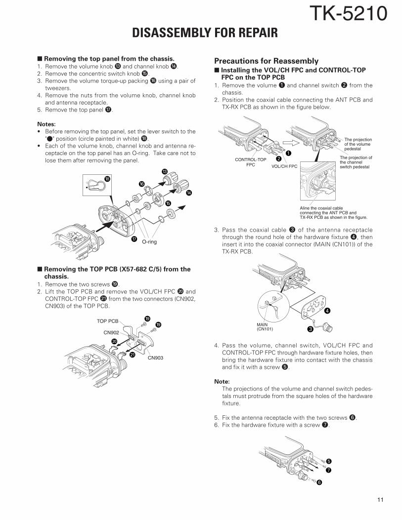
Removing the top panel from the chassis.1. Remove the volume knob ç and channel knob √.2. Remove the concentric switch knob ∫.3. Remove the volume torque-up packing ~ using a pair of
tweezers.4. Remove the nuts from the volume knob, channel knob
and antenna receptacle.5. Remove the top panel µ.
Notes:
• Before removing the top panel, set the lever switch to the"-" position (circle painted in white) ≤.
• Each of the volume knob, channel knob and antenna re-ceptacle on the top panel has an O-ring. Take care not tolose them after removing the panel.
Removing the TOP PCB (X57-682 C/5) from thechassis.
1. Remove the two screws ≥.2. Lift the TOP PCB and remove the VOL/CH FPC ÷ and
CONTROL-TOP FPC 21 from the two connectors (CN902,CN903) of the TOP PCB.
Precautions for Reassembly Installing the VOL/CH FPC and CONTROL-TOP
FPC on the TOP PCB
1. Remove the volume z and channel switch x from thechassis.
2. Position the coaxial cable connecting the ANT PCB andTX-RX PCB as shown in the figure below.
3. Pass the coaxial cable c of the antenna receptaclethrough the round hole of the hardware fixture v, theninsert it into the coaxial connector (MAIN (CN101)) of theTX-RX PCB.
4. Pass the volume, channel switch, VOL/CH FPC andCONTROL-TOP FPC through hardware fixture holes, thenbring the hardware fixture into contact with the chassisand fix it with a screw b.
Note:
The projections of the volume and channel switch pedes-tals must protrude from the square holes of the hardwarefixture.
5. Fix the antenna receptacle with the two screws n.6. Fix the hardware fixture with a screw m.
O-ring
ç
√
∫
µ
≤~
CN902
TOP PCB
CN903
≥
÷
21
≥
CONTROL-TOPFPC VOL/CH FPC
The projection of the volume pedestal
The projection of the channelswitch pedestal
Aline the coaxial cable connecting the ANT PCB and TX-RX PCB as shown in the figure.
zx
MAIN(CN101) c
v
b
n
m

TK-5210
12
DISASSEMBLY FOR REPAIR
7. Insert the VOL/CH FPC , and the CONTROL-TOP FPC .into the connectors (CN902, CN903) of the TOP PCB.
8. Fix the TOP PCB with a screw /.9. Fix the TOP PCB with a screw Ω.
TX-RX PCB Installation Procedure1. Insert the coaxial cable of the antenna receptacle into the
coaxial connector (CN101) of the TX-RX PCB z and thecoaxial cable of the ANT PCB into the coaxial connector(CN102) of the TX-RX PCB x.
2. Grasp both sides of the lower part of the TX-RX PCB, tiltthe TX-RX PCB and install the chassis so that the PTT FPCc, CONTROL-TOP FPC v and universal connector FPCb are not caught n.
3. Fix the TX-RX PCB with the 14 screws.
LCD ASSY Installation Procedure (K2 and K3
models only)
1. Fold the LCD ASSY FPC to the back of the holder z sothat the FPC is between the two tabs on the right side ofthe holder x.
2. Fit the two tabs on the right side of the holder c and thetwo tabs on the left side of the holder v into theCONTROL PCB.
Note:
Take care that the FPC is not caught when fitting the twotabs on the right side of the holder.
3. Insert the FPC into the CONTROL PCB connector (CN751)b.
Main Packing (G53-1637-04) Installation Procedure
1. Hook the packing (coated with silicon oil) in the uppergroove of the chassis z, then fit the packing into thelower groove of the chassis x.
Note:
Ensure that the chassis grooves and packing are free fromdirt and dust.
2. Fit the packing into the grooves on both sides of thechassis c. (Fit the packing into the groove in the chassisby tracing it lightly with your fingers.)
Note:
To remove the packing from the chassis groove, use aresin adjustment bar or other such device. If the packingis pried with a sharp metallic tool, such as tweezers, thepacking may become damaged.
3. Verify that the packing fits snuggly into the groove of thechassis.
CN902
CN903
,
/Ω
.
CN102
CN101
Grasp both sides of the lower part of the TX-RX PCB
z
x
c
v
n
b
LCD ASSY FPCtab
tab
zx
CN751
b
Main packing
z
c
c
x
tab
CONTROL PCB
c
vv
c

TK-5210
13
2. Tighten the two screws from the TX-RX PCB side.
3. Firmly tighten the hexagon screws of the GND terminal.
Installation Procedure during Parts
Replacement
Attaching the Sheet (G10-1338-04, J99-0383-14)to the Front Case Speaker and Installation ofthe Packing (G53-1633-04)
1. Attach a new fiber sheet z (G10-1338-04) so that itsconvex fits the hollow of the front case x.
2. Attach a new pressure sensitive adhesive sheet c (J99-0383-14) so that its convex fits the hollow of the frontcase v.
3. Remove the separation sheet from the pressure sensitiveadhesive sheet with a pair of tweezers b.
4. Fit the packing n (G53-1633-04) into the front casespeaker.
Note:
Fit the packing into the hollow of the case so that the twolow-height places in the convex of the packing are posi-tioned on the lower side m.
5. Verify that the packing does not ride on the rib of the case.
Installing a new LCD ASSY to the holder (K2and K3 models only)
1. Remove the separation paper (brown) from the new sheetz x, and attach the sheet to the surface of the holder c.
2. Remove the protection sheets attached to both sides ofthe new LCD ASSY.
DISASSEMBLY FOR REPAIR
Top Packing (G53-1638-04) Installation Procedure1. Ensure that the hardware fixture is first secured to the
chassis.2. Hook the packing (coated with silicon oil) in the upper left
groove of the chassis z, then fit the packing into the rightgroove of the chassis. x
Notes:
• Verify that the chassis grooves and packing are free fromdirt and dust.
• To remove the packing from the chassis groove, use aresin adjustment bar or other such device. If the packingis pried with a sharp metallic tool, such as tweezers, thepacking may become damaged.
3. Verify that the packing fits snuggly into the groove of thechassis.
Volume Torque-up Packing (G53-1628-04)Installation Procedure
Insert the packing using a pair of tweezers so that thehollow of the packing fits the convex of the panel z.
Screw sequence for mounting the batteryterminal block to the chassis.
Attach the battery terminal block to the chassis asdescribed in the following procedure.
1. Loosely fix the hexagon screws of the GND terminal tothe chassis (enough so that the hexagon screws do notmove).
Volume torque-up packing z
GND terminal
Two screws
n
c
v bz
m
x
Top packing
Hardware fixture
z
x
TK-5210
14
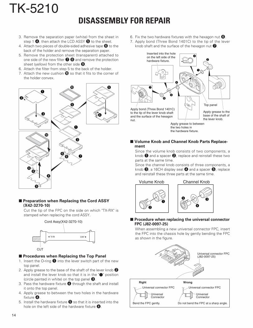
3. Remove the separation paper (white) from the sheet instep 1 v, then attach the LCD ASSY b to the sheet.
4. Attach two pieces of double-sided adhesive tape n to theback of the holder and remove the separation paper.
5. Remove the protection sheet (transparent) attached toone side of the new filter m , and remove the protectionsheet (yellow) from the other side ..
6. Attach the filter from step 5 to the back of the holder.7. Attach the new cushion / so that it fits to the corner of
the holder convex.
Preparation when Replacing the Cord ASSY(X42-3270-10)
Cut the tip of the FPC on the side on which "TX-RX" isstamped when replacing the cord ASSY.
Procedures when Replacing the Top Panel1. Insert the O-ring z into the lever switch part of the new
top panel.2. Apply grease to the base of the shaft of the lever knob x
and install the lever knob so that it is in the "-" position(circle painted in white) on the top panel c.
3. Pass the hardware fixture v through the shaft and installit onto the top panel.
4. Apply grease to between the two holes in the hardwarefixture v.
5. Install the hardware fixture b so that it is inserted into thehole on the left side of the hardware fixture v.
z
z
x
c
c
v
n mn
n
,
.
n
b
b/
/
CUT
TX-RX CONT
Cord Assy(X42-3270-10)
6. Fix the two hardware fixtures with the hexagon nut n.7. Apply bond (Three Bond 1401C) to the tip of the lever
knob shaft and the surface of the hexagon nut m.
Volume Knob and Channel Knob Parts Replace-ment
Since the volume knob consists of two components, aknob z and a spacer x, replace and reinstall these twoparts at the same time.Since the channel knob consists of three components, aknob c, a 16CH display seal v and a spacer b, replaceand reinstall these three parts at the same time.
Procedure when replacing the universal connectorFPC (J82-0097-25)
When assembling a new universal connector FPC, insertthe FPC into the chassis hole by gently bending the FPCas shown in the figure.
Apply grease to between the two holes in the hardware fixture.
Apply bond (Three Bond 1401C) to the tip of the lever knob shaft and the surface of the hexagon nut.
Top panel
Inserted into the hole on the left side of the hardware fixture.
Apply grease to the base of the shaft of the lever knob.
z
v
m
b
n
x
c
Volume Knob Channel Knob
zcb
vx
DISASSEMBLY FOR REPAIR
UniversalConnector
Do not bend the FPC at a sharp angle.
Universal connector FPC
Wrong
UniversalConnector
Bend the FPC gently.
Universal connector FPC
Universal connector FPC(J82-0097-25)
Right
TK-5210
15
CIRCUIT DESCRIPTION
1. OverviewThis transceiver is a VHF/FM/P25 portable transceiver
designed to operate in the frequency range of 136 to174MHz.
The unit consists of receiver, transmitter, phase-lockedloop (PLL) frequency synthesizer, base band parts, powersupply, and control circuits.
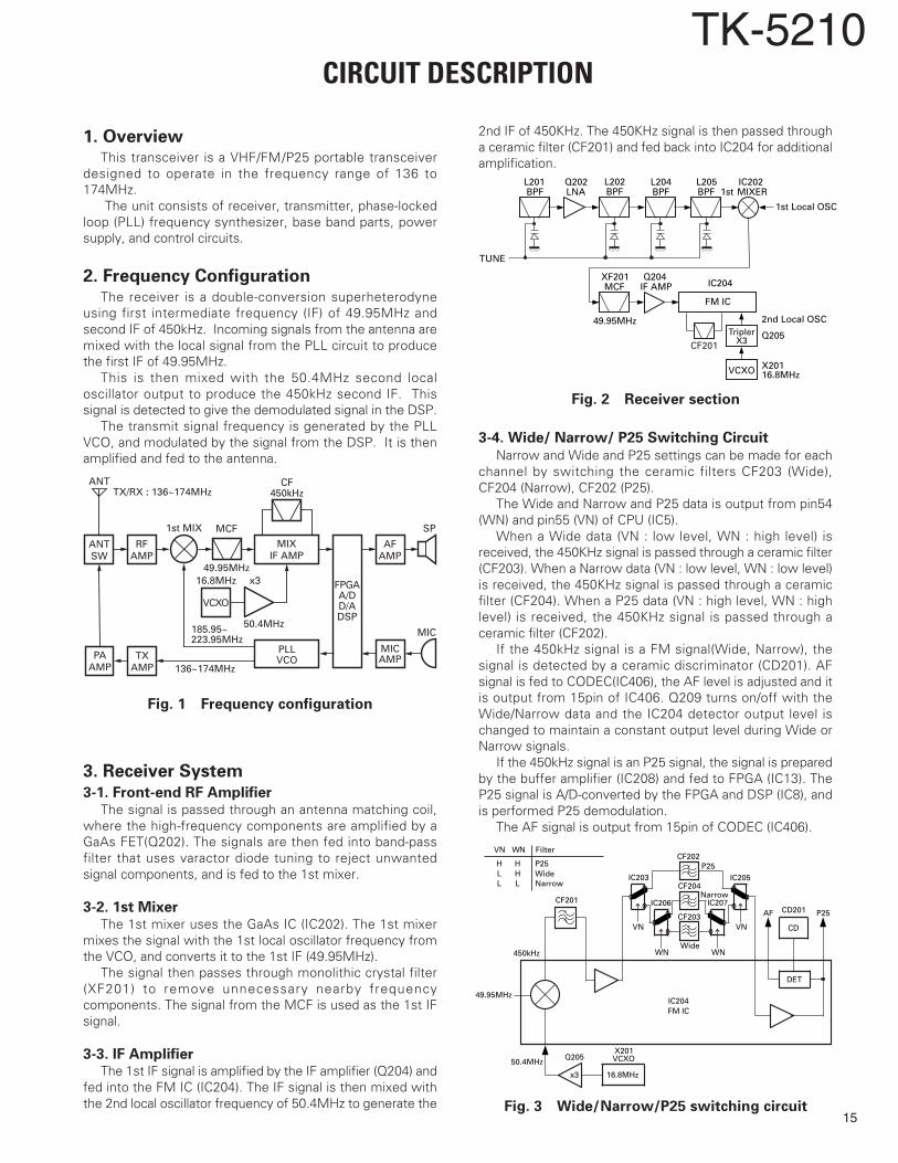
2. Frequency ConfigurationThe receiver is a double-conversion superheterodyne
using first intermediate frequency (IF) of 49.95MHz andsecond IF of 450kHz. Incoming signals from the antenna aremixed with the local signal from the PLL circuit to producethe first IF of 49.95MHz.
This is then mixed with the 50.4MHz second localoscillator output to produce the 450kHz second IF. Thissignal is detected to give the demodulated signal in the DSP.
The transmit signal frequency is generated by the PLLVCO, and modulated by the signal from the DSP. It is thenamplified and fed to the antenna.
3. Receiver System
3-1. Front-end RF AmplifierThe signal is passed through an antenna matching coil,
where the high-frequency components are amplified by aGaAs FET(Q202). The signals are then fed into band-passfilter that uses varactor diode tuning to reject unwantedsignal components, and is fed to the 1st mixer.
3-2. 1st MixerThe 1st mixer uses the GaAs IC (IC202). The 1st mixer
mixes the signal with the 1st local oscillator frequency fromthe VCO, and converts it to the 1st IF (49.95MHz).
The signal then passes through monolithic crystal filter(XF201) to remove unnecessary nearby frequencycomponents. The signal from the MCF is used as the 1st IFsignal.
3-3. IF AmplifierThe 1st IF signal is amplified by the IF amplifier (Q204) and
fed into the FM IC (IC204). The IF signal is then mixed withthe 2nd local oscillator frequency of 50.4MHz to generate the
Fig. 1 Frequency configuration
ANTTX/RX : 136~174MHz
ANTSW
RFAMP
PAAMP
TXAMP
1st MIX MCF
VCXO
49.95MHz
CF450kHz
MIXIF AMP
AFAMP
SP
16.8MHz
50.4MHz
x3
185.95~223.95MHz
136~174MHz
PLLVCO
FPGAA/DD/ADSP
MICAMP
MIC
2nd IF of 450KHz. The 450KHz signal is then passed througha ceramic filter (CF201) and fed back into IC204 for additionalamplification.
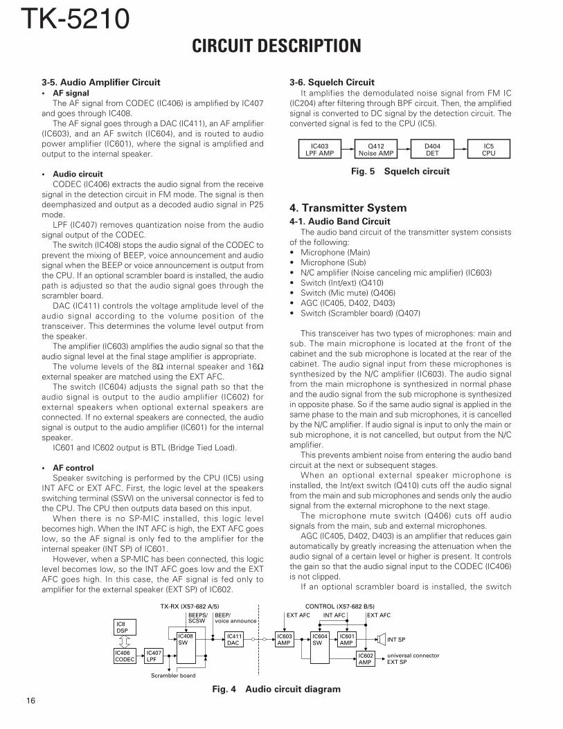
3-4. Wide/ Narrow/ P25 Switching Circuit
Narrow and Wide and P25 settings can be made for eachchannel by switching the ceramic filters CF203 (Wide),CF204 (Narrow), CF202 (P25).
The Wide and Narrow and P25 data is output from pin54(WN) and pin55 (VN) of CPU (IC5).
When a Wide data (VN : low level, WN : high level) isreceived, the 450KHz signal is passed through a ceramic filter(CF203). When a Narrow data (VN : low level, WN : low level)is received, the 450KHz signal is passed through a ceramicfilter (CF204). When a P25 data (VN : high level, WN : highlevel) is received, the 450KHz signal is passed through aceramic filter (CF202).
If the 450kHz signal is a FM signal(Wide, Narrow), thesignal is detected by a ceramic discriminator (CD201). AFsignal is fed to CODEC(IC406), the AF level is adjusted and itis output from 15pin of IC406. Q209 turns on/off with theWide/Narrow data and the IC204 detector output level ischanged to maintain a constant output level during Wide orNarrow signals.
If the 450kHz signal is an P25 signal, the signal is preparedby the buffer amplifier (IC208) and fed to FPGA (IC13). TheP25 signal is A/D-converted by the FPGA and DSP (IC8), andis performed P25 demodulation.
The AF signal is output from 15pin of CODEC (IC406).
1st Local OSC
BPF BPF BPF 1stLNA MIXERQ202L201
TUNE
L204 L205 IC202
MCFXF201
49.95MHz
IF AMPQ204
Q205
2nd Local OSC
FM IC
IC204
TriplerX3CF201
BPFL202
X20116.8MHzVCXO
WN WN
VNVNCF203
CF204
CF202P25
Narrow
Wide
IC203 IC205
IC206 IC207CF201
16.8MHz
VCXOX201
x3
Q20550.4MHz
49.95MHz
450kHz
IC204FM IC
DET
P25
CD
CD201AF
VN WN
L
H HL H
LWideNarrow
P25
Filter
Fig. 2 Receiver section
Fig. 3 Wide/Narrow/P25 switching circuit
TK-5210
16
CIRCUIT DESCRIPTION
3-5. Audio Amplifier Circuit• AF signal
The AF signal from CODEC (IC406) is amplified by IC407and goes through IC408.
The AF signal goes through a DAC (IC411), an AF amplifier(IC603), and an AF switch (IC604), and is routed to audiopower amplifier (IC601), where the signal is amplified andoutput to the internal speaker.
• Audio circuit
CODEC (IC406) extracts the audio signal from the receivesignal in the detection circuit in FM mode. The signal is thendeemphasized and output as a decoded audio signal in P25mode.
LPF (IC407) removes quantization noise from the audiosignal output of the CODEC.
The switch (IC408) stops the audio signal of the CODEC toprevent the mixing of BEEP, voice announcement and audiosignal when the BEEP or voice announcement is output fromthe CPU. If an optional scrambler board is installed, the audiopath is adjusted so that the audio signal goes through thescrambler board.
DAC (IC411) controls the voltage amplitude level of theaudio signal according to the volume position of thetransceiver. This determines the volume level output fromthe speaker.
The amplifier (IC603) amplifies the audio signal so that theaudio signal level at the final stage amplifier is appropriate.
The volume levels of the 8Ω internal speaker and 16Ωexternal speaker are matched using the EXT AFC.
The switch (IC604) adjusts the signal path so that theaudio signal is output to the audio amplifier (IC602) forexternal speakers when optional external speakers areconnected. If no external speakers are connected, the audiosignal is output to the audio amplifier (IC601) for the internalspeaker.
IC601 and IC602 output is BTL (Bridge Tied Load).
• AF control
Speaker switching is performed by the CPU (IC5) usingINT AFC or EXT AFC. First, the logic level at the speakersswitching terminal (SSW) on the universal connector is fed tothe CPU. The CPU then outputs data based on this input.
When there is no SP-MIC installed, this logic levelbecomes high. When the INT AFC is high, the EXT AFC goeslow, so the AF signal is only fed to the amplifier for theinternal speaker (INT SP) of IC601.
However, when a SP-MIC has been connected, this logiclevel becomes low, so the INT AFC goes low and the EXTAFC goes high. In this case, the AF signal is fed only toamplifier for the external speaker (EXT SP) of IC602.
3-6. Squelch CircuitIt amplifies the demodulated noise signal from FM IC
(IC204) after filtering through BPF circuit. Then, the amplifiedsignal is converted to DC signal by the detection circuit. Theconverted signal is fed to the CPU (IC5).
4. Transmitter System
4-1. Audio Band CircuitThe audio band circuit of the transmitter system consists
of the following:• Microphone (Main)• Microphone (Sub)• N/C amplifier (Noise canceling mic amplifier) (IC603)• Switch (Int/ext) (Q410)• Switch (Mic mute) (Q406)• AGC (IC405, D402, D403)• Switch (Scrambler board) (Q407)
This transceiver has two types of microphones: main andsub. The main microphone is located at the front of thecabinet and the sub microphone is located at the rear of thecabinet. The audio signal input from these microphones issynthesized by the N/C amplifier (IC603). The audio signalfrom the main microphone is synthesized in normal phaseand the audio signal from the sub microphone is synthesizedin opposite phase. So if the same audio signal is applied in thesame phase to the main and sub microphones, it is cancelledby the N/C amplifier. If audio signal is input to only the main orsub microphone, it is not cancelled, but output from the N/Camplifier.
This prevents ambient noise from entering the audio bandcircuit at the next or subsequent stages.
When an optional external speaker microphone isinstalled, the Int/ext switch (Q410) cuts off the audio signalfrom the main and sub microphones and sends only the audiosignal from the external microphone to the next stage.
The microphone mute switch (Q406) cuts off audiosignals from the main, sub and external microphones.
AGC (IC405, D402, D403) is an amplifier that reduces gainautomatically by greatly increasing the attenuation when theaudio signal of a certain level or higher is present. It controlsthe gain so that the audio signal input to the CODEC (IC406)is not clipped.
If an optional scrambler board is installed, the switch
Fig. 4 Audio circuit diagram
Fig. 5 Squelch circuit
IC403LPF AMP
Q412Noise AMP
D404DET
IC5CPU
BEEPS/SCSW
TX-RX (X57-682 A/5) CONTROL (X57-682 B/5)BEEP/voice announce
EXT AFC EXT AFC
INT SP
IC406CODEC
IC407LPF
IC411DAC
IC603AMP
IC604SW
universal connectorEXT SP
Scrambler board
IC8DSP
INT AFC
IC601AMP
IC602AMP
IC408SW

TK-5210
17
CIRCUIT DESCRIPTION
(Q407) adjusts the signal path so that the audio signal is inputto the CODEC through the scrambler board.
The audio signal is input to the CODEC (base band circuit)through the above path.
4-2. Base Band CircuitThe base band circuit of the transmitter system consists
of the following:• CODEC (IC406)• DSP (IC411)• LPF (IC407)• Buffer (IC409)• DAC (IC411)• Amplifier (IC412)
The audio signal output from the base band circuit isconverted to digital data of a sampling frequency of 48 kHzand a quantization resolution of 16 bits by the CODEC(IC406). This digital data is sent to the DSP (IC8), and voicesignals of 300 Hz or lower and frequencies of 3 kHz or higherare cut off and an audio range 300 Hz to 3 kHz is extracted.
The audio signal is then pre-emphasized in FM mode andsynthesized with the signals, such as QT and DQT, asrequired, and is then output from the CODEC. In P25 mode,the audio signal is converted to the C4FM base band signaland output from the CODEC. The DTMF and MSK base bandsignals are also generated by the DSP and output by theCODEC.
LPF (IC407) removes quantization noise from the baseband signal output from the CODEC.
The buffer (IC409) sets the base band signal level to theDAC input range.
The DAC (IC411) assigns the base band signal to the VCO(Q311) and VCXO (X301).
At this time, the level output according to the transmitcarrier is fine-adjusted according to the modulation methodof FM Wide, FM Narrow and P25.
4-3. Transmit Signal Amplification Circuit
(From T/R switch to Final amplifier) The transmit signal passing through the T/R switch
(D101) is amplified to approx. 50 mW by the two transistoramplification circuits (Q101, Q102). The transmit signaloutput from Q102 passes through a 3dB attenuator toimprove high-frequency signal matching is amplified by thedrive amplifier (Q103) and applied to the final amplifier(Q105). The signal applied to the final amplifier is amplified bythe final amplifier so that the antenna output is 5 W (1 W forLow Power).
4-4. High-Frequency Signal Switch Circuit
(From Antenna switch to ANT output)The transmit signal output from the final amplifier (Q105)
passes through the antenna switch (D106, D107) and LPF,and goes into the SPDT switch (IC102, IC103) which changesthe antenna connector (CN101) and the universal connector(CN102).
The transmit signal passing through the output changeswitch passes through the surge protection HPF andspurious removing LPF and then goes to the antennaconnector (CN101) or the universal connector (CN102),specified by the SPDT switch (IC102, IC103).
4-5. APC CircuitThe APC circuit detects the current of the drive amplifier
(Q103) and final amplifier (Q105) during transmission andcontrols the output power by controlling the current.
It detects the current using R119 and R120 and applies adrop voltage between both resistors during transmission toAPC (IC101). It controls the transmission current of the driveamplifier and final amplifier so that it is constant bycomparing this current with the reference voltage outputfrom pin 7 of IC104. The reference voltage input to pin 5 ofIC104 is output from the DAC (IC411). High/Low poweroutput is set according to the DAC output voltage.
4-6. Temperature Protection CircuitThe temperature protection circuit reduces the APC
voltage when the temperature of Q105 rises, to preventthermal destruction of the final amplifier (Q105). The CPU
Fig. 6 Audio band and Base band circuit
Fig. 7 Transmitter circuit
MIC(MAIN)
EXT.MIC
MIC(SUB)
MSW/CTSMM
IC603 Q410SW
Q406SW AGC-AMP
IC405LPF
D402,D403DET
Scrambler board
SCSW
MIC
N/CAMP
IC411DAC
Q407SW
IC8DSP
IC406CODEC
IC407LPF
IC409BUFF
IC412AMP
X301VCXO
Q311VCO
D101T/R SW
Q103Drive Amp
Q105Final Amp D106,D107
ANT SW
IC101APCR119
+B
R120APC SW
Q101Pre Pre Drive Amp
Q102Pre Drive Amp 3dB
Attenuator
IC102,IC103SPDT
CN101
CN102LPF
(IC5) detects the temperature with a thermistor (TH101) tocontrol the reference voltage to the APC circuit.

TK-5210
18
CIRCUIT DESCRIPTION
5. PLL Frequency SynthesizerThe PLL Frequency Synthesizer consists of the following
components:• VCXO (X301)• VCO (Q310, Q311)• Rheostat (IC414)• PLL IC (IC303)• 1/2 divider (IC304)• Local switch (D101, D210)
5-1. VCXO (X301)VCXO (X301) generates a reference frequency of 16.8
MHz for the PLL frequency synthesizer. This referencefrequency is applied to pin 8 of the PLL IC (IC303).
The VCXO oscillation frequency is fine-adjusted bycontrolling the voltage applied to pin 1 of the VCXO with DAC(IC411). It is also controlled with pin 1 of the VCXO if theoutput from VCXO is modulated.
5-2. VCOThere is a RX VCO and a TX VCO.The TX VCO (Q311) generates a transmit carrier and the
RX VCO (Q310) generates a 1st local receive signal.For the VCO oscillation frequency, the transmit carrier is
272 to 348 MHz and the 1st local receive signal is 371.9 to447.9 MHz.
The VCO oscillation frequency is determined by onesystem of operation switching terminal "T/R" and twosystems of voltage control terminals "C/V" and "V-assist".
The operation switching terminal, "T/R", is controlled bythe control line (T/R) output from the CPU (IC5). When the T/R logic is low, the VCO outputs the transmit carrier and whenit is high, it outputs a 1st local receive signal.
The voltage control terminals, "CV" and "V-assist", arecontrolled by the PLL IC (IC303) and rheostat (IC414) and theoutput frequency changes continuously according to theapplied voltage. For the modulation input terminal, "MOD",the output frequency changes according to the appliedvoltage. This is used to modulate the VCO output. "MOD"works only when "T/R" is low.
5-3. Rheostat (IC414)The rheostat (IC414) is connected to the VCO voltage
control terminal, "V-assist", and quickly controls the VCOoscillation frequency. However, its accuracy is low and theVCO frequency cannot be matched accurately with thedesired transmit carrier or the 1st local receive signal.
The rheostat is controlled by the CPU (IC5) through the 3-line "PCS", "DAT", "CLK" serial bus.
5-4. PLL IC (IC303)PLL IC compares the differences in phases of the VCO
oscillation frequency and the VCXO reference frequency,returns the difference to the VCO CV terminal and realizesthe "Phase Locked Loop" for the return control. This allowsthe VCO oscillation frequency to accurately match (lock) thedesired frequency.
When the frequency is controlled by the PLL, thefrequency convergence time increases as the frequency
difference increases when the set frequency is changed. Tosupplement this, the rheostat is used before control by thePLL IC to bring the VCO oscillation frequency close to thedesired frequency. As a result, the VCO CV voltage does notchange and is always stable at approx. 2 V.
The desired frequency is set for the PLL IC by the CPU(IC5) through the 3-line "LE", "DAT", "CLK" serial bus. Whetherthe PLL IC is locked or not is monitored by the CPU throughthe “UL” signal line. If the VCO is not the desired frequency(unlock), the "UL" logic is low.
5-5. 1/2 divider (IC304)The 1/2 divider (IC304) inputs the transmit carrier and the
1st local receive signal output from the VCO and divides eachfrequency by 1/2. The frequency divided by 1/2 becomes acarrier that is actually sent and a 1st local receive signal that isactually input to a mixer. (Both the VCO and the PLL ICoperate with double frequencies in phase locked loops.)
5-6. Local Switch (D101, D210)The connection destination of the signal output from the
1/2 divider (IC304) is changed with the diode switch (D101)that is controlled by the transmission power supply, 5T, andthe diode switch (D210) that is controlled by the receivepower supply, 5R.
If the 5T logic is high, it is connected to a send-side pre-pre-drive (Q101). If the 5T logic is low, it is connected to areceive-side mixer (IC202).
6. Control CircuitThe control circuit consists of CPU (IC5) and its peripheral
circuits. It controls the TX-RX unit and transfers data to theControl unit. IC5 mainly performs the following;1) Switching between transmission and reception by PTT
signal input.2) Reading system, zone, frequency, and program data from
the memory circuit.3) Sending frequency program data to the PLL.4) Controlling squelch on/off by the DC voltage from the
squelch circuit.5) Controlling the audio mute circuit by decode data input.6) Transmitting tone and encode data.
6-1. Memory CircuitMemory circuit consists of the CPU (IC5) and a flash
memory (IC6). A flash memory has a capacity of 16M bits and
Fig. 8 PLL block diagram
T/R
IC414 V-assist TX: 272~348MHzRX: 371.9~447.9MHzRHE
PCSDATCLK
LEDATCLK
IC304 Q314 D101 to pre-pre-driveLPF VCO 1/2 BUFF SW
UL CV
IC5
IC303 Q312 D210 to 1st mixer
(Q101)
(IC202)
CPU
PLLLPF
BUFF SW
MOD
X301 IC411VCXO DAC

TK-5210
19
CIRCUIT DESCRIPTION
contains the transceiver control program for the CPU. It alsostores the data for transceiver channels and operating param-eter that are written by the FPU. This program can be easilywritten from an external devices.
The EEPROM (IC2) stores the last channel data, the scanon status, and other parameters.
Flash memoryNote : The flash memory stores the data that is written bythe FPU (KPG-95D), and firmware program (User mode, Testmode, Tuning mode, etc.). This data must be rewritten whenreplacing the flash memory.
EEPROMNote : The EEPROM stores tuning data (Deviation, Squelch,etc.).Realign the transceiver after replacing the EEPROM.
Real-time clockThe clock function is based on real-time clock IC (IC1).
When the power supply is off, it is backed up by an internalsecondary lithium battery
6-2. LCD (K2 and K3 models only)The LCD is controlled using the bus lines on the connector
(CN604) of the control unit (X57 B/5).It corrects the LCD contrast voltage using IC704. The
voltage corresponding to the temperature is sent to pin 3 ofIC704 from the CPU (IC5) according to the temperaturemeasurement results using a temperature IC (IC4).
6-3. Temperature Detection CircuitThe temperature detect ion circuit detects the
temperature using a temperature IC (IC4) and corrects thethermal characteristic change of the squelch or LCD.
6-4. Key Detection CircuitKeys are detected using three shift registers (IC701,
IC702, IC703).The KIN signal that is normally pulled down goes high
when any key is pressed.
6-5. Low Battery WarningThe battery voltage is divided using R15 and R16 and is
detected by the CPU (IC5). When the battery voltage fallsbelow the voltage set by the Low battery warningadjustment, the red LED blinks to notify the operator that it istime to replace the battery. If the battery voltage falls evenmore (approx. 5.8V), a beep sounds and transmission stops.
Low battery warning Battery condition
The red LED blinks during The battery voltage is low but
transmission. the transceiver is still usable.
The red LED blinks and The battery voltage is low and
the warning tone beeps while the transceiver is not usable to
the PTT switch is pressed. make calls.
6-6. Battery Type DetectionThe transceiver automatically detects the battery type,
measuring the resistance between the S-terminal and GNDterminal on the battery pack and changes the suppliedvoltage to the S-terminal as below. The microprocessor thendetects the battery type.
6-7. VOXThe VOX function can be used only with an external
microphone.The VOX (Voice Operated Transmission) function detects
voice input to the microphone and automatically switchesbetween transmission and reception. However, if ascrambler board is installed (Extended Function VoiceScrambler is selected with FPU), VOX does not operate.
If the microphone input exceeds a certain level,transmission automatically begins. If the input falls below acertain level, the transceiver automatically returns to receivemode.
The TK-5210 realizes this function using DSP (IC8).
6-8. DSPThe DSP circuit consists of a DSP (IC8), a CODEC (IC406)
and processes the base band signal. The DSP operates on anexternal clock of 9.216MHz (the same as the CPU), the I/Osection operates at 3.3V and the core section operates at1.5V. The DSP carries out the following processes:• C4FM encoding
Fig. 9 Memory circuit
CPU EEPROM
FLASH
IC5
IC6
IC2
Fig. 10 Clock diagram
IC406CODEC
IC13FPGA
IC8DSP
IC5CPU
IC14(2/3,3/3)9.216MHz
9.216MHz
18.432MHz
18.432MHz
18.432MHz
IC12X2
VCXOIC14(1/3)
Battery type Input voltage of S-terminal Resistor value
Battery case 0~0.2V Short
Li-ion battery 0.85~1.02V 47 kΩ
Ni-Cd battery 3.23~3.37V Open
Ni-MH battery 1.71~1.95V 150 kΩ
TK-5210
20
CIRCUIT DESCRIPTION
• Analog FM pre-emphasis/de-emphasis• Vocoder (IMBE) processing between audio codec and
modulation/demodulation• CAI processing, such as error correction encoding• QT/DQT encoding/decoding• DTMF encoding/decoding• MSK encoding/decoding• 2-tone decoding• Compressor/expander processing• Transmit/receive audio filtering processing• VOX processing• Microphone amplifier AGC processing• Audio mute processing• Modulation level processing
6-9. FPGAThe FPGA(IC13) I/O section operates at 3.3V. and the core
section operates at 2.5V. The FPGA has the following func-tion.• Demodulation (C4FM,CQPSK)• Shift register(8CH)• Level convert Buffer amplifier(5V3.3V)(9CH)• Generates 1.536MHz for the demodulation and CODEC.
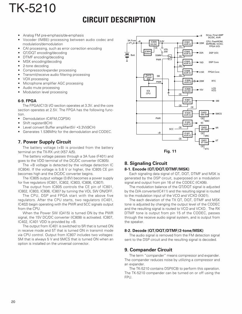
7. Power Supply CircuitThe battery voltage (+B) is provided from the battery
terminal on the TX-RX unit (X57 A/5).The battery voltage passes through a 3A fuse (F401) and
goes to the VDD terminal of the DC/DC converter (IC805).The +B voltage is detected by the voltage detection IC
(IC804). If the voltage is 5.6 V or higher, the IC805 CE pinbecomes high and the DC/DC converter begins.
The IC805 output voltage (3.6V) becomes a power supplyfor five regulators (IC801, IC802, IC803, IC806, IC807).
The output from IC805 controls the CE pin of IC801,IC802, IC803, IC806, IC807 by turning the VOL SW ON/OFF.
The CPU, DSP and FPGA start with the above fiveregulators. After the CPU starts, two regulators (IC401,IC402) begin operating with the PWR and 5CC signals outputfrom the CPU.
When the Power SW (Q415) is turned ON by the PWRsignal, the 15V DC/DC converter (IC808) is activated. IC807,IC402, IC401 VDD is provided by +B.
The output from IC401 is switched to 5R that is turned ONin receive mode and 5T that is turned ON in transmit modevia CPU control. Output from IC807 includes two voltages:5M that is always 5 V and 5MCS that is turned ON when anoption is installed on the universal connector.
Fig. 11
8. Signaling Circuit
8-1. Encode (QT/DQT/DTMF/MSK)Each signaling data signal of QT, DQT, DTMF and MSK is
generated by the DSP circuit, superposed on a modulationsignal and output from pin 16 of the CODEC (IC406).
The modulation balance of the QT/DQT signal is adjustedby the D/A converter(IC411) and the resulting signal is routedto the modulation input of the VCO and VCXO (X301).
The each deviation of the TX QT, DQT, DTMF and MSKtone is adjusted by changing the output level of the CODECand the resulting signal is routed to VCO and VCXO. The RXDTMF tone is output from pin 15 of the CODEC, passesthrough the receive audio signal system, and is output fromthe speaker.
8-2. Decode (QT/DQT/DTMF/2-tone/MSK)The audio signal is removed from the FM detection signal
sent to the DSP circuit and the resulting signal is decoded.
9. Compander CircuitThe term “compander” means compressor and expander.
The compander reduces noise by utilizing a compressor andan expander.
The TK-5210 contains DSP(IC8) to perform this operation.The TK-5210 compander can be turned on or off using theFPU.
CPU, FlashROM,EEPROM, VCXO,
FPGA (I/O)
DSP (I/O)
DSP Core
FPGA Core
LCDVCO
Drive, Final AMPDC/DC, AVR
3.6VIC805DC/DC
IC804Detect
+B3A Fuse
Batt
5M
5MCS
5R
5T
33M
33A
15D
2.5D
+B
15V
5C
5CC
CE
CE
5RC
5TC
CE5MC
CECE
CE
CE
CE
CE
CE
CE
CE
CE
S36M
PWR
PWR
Q415Power
SWSB
IC5CPU
VOLSW
PWR
+B
IC801AVR IC
Q4025R SW
Q4015T SW
Q4035M SW
IC802AVR IC
IC803AVR IC
IC806AVR IC
IC402AVR IC
IC520AVR IC
IC401AVR IC
IC807AVR IC
IC808
RTC28MIC606
DC/DC
AVR IC

TK-5210
21
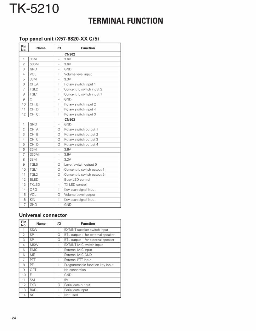
TERMINAL FUNCTION
TX-RX unit (X57-6820-XX A/5) Pin Name I/O FunctionNo.Pin Name I/O FunctionNo.CN7
1 DSR I Data set ready2 E - GND3 RXD I Serial data input4 TXD O Serial data Output5 5M - 5V6 RTS1 O Request to Send7 REM I Programmable function key input8 PTT I External PTT input9 MICE - External MIC GND10 EMC I External MIC input11 MSW/CTS I EXT/INT MIC switch input12 SP- O BTL output - for external speaker13 SP+ O BTL output + for external speaker14 SSW I EXT/INT speaker switch input
CN14
1 OPT1 O Scramble code output 1 (Scrambler board)O Channel busy (ANI board)I Busy (VGS-1)
2 OPT3 O Scramble code output 2 (Scrambler board)I Key (ANI board)I Play (VGS-1)
3 RXD1 I Serial data input(VGS-1)4 TXD1 O PTT (Scrambler board)
O Serial data output (VGS-1)5 NC - No connection6 OPT4 I/O Echo PTT (Scrambler board)
O PTT (ANI board)O Enable (VGS-1)
7 USEL - GND8 OPT5 O Scramble code output 4 (Scrambler board)
O Emergency (ANI board)O Reset output(VGS-1)
9 DGND - GND10 AGND - GND11 AI I VGS Audio Input (VGS-1)12 AO O VGS Audio Output (VGS-1)13 AGND - GND14 5A - 5V15 STON I Side tone input(ANI board)16 DI/ANI I Data input (ANI board)17 TCONT I Speaker mute signal (ANI board)18 MAN DOWN O Man-down output (ANI board)19 INH I MIC mute signal input (ANI board)20 OPT2 O Scrambler control signal output
(Scrambler board)I Emergency signal input (ANI board)
21 TXO O MIC signal output (Scrambler board)22 RXEO O Audio signal output (Scrambler board)23 RXEI I Audio signal input (Scrambler board)24 TXI I MIC signal input (Scrambler board)25 OPT6 O Scramble code output 3 (Scrambler board)
26 SB2 O Switched B output
CN15 (for production)
1~20
CN19 (K2 and K3 models only)
1 LCS O LCD chip select2 GND - GND3 D0 I/O Data bus 04 D1 I/O Data bus 15 D2 I/O Data bus 26 D3 I/O Data bus 37 D4 I/O Data bus 48 D5 I/O Data bus 59 D6 I/O Data bus 610 D7 I/O Data bus 711 RD - No connection12 WR O WR bus13 GND - GND14 A0 O Address bus 0
CN408
1 GND - GND2 GND - GND3 MIC I External MIC input4 MICE - External MIC GND5 SP+ I BTL output + for external speaker6 PWR O Power control output7 SP+ I BTL output + for external speaker8 15V - 15V9 SP- I BTL output - for external speaker10 SB1 I Battery level input11 SP- I BTL output - for external speaker12 +B - Power input after passing through the fuse13 AF O Audio Output14 +B - Power input after passing through the fuse15 VOL I Volume level input16 +B - Power input after passing through the fuse17 CLK O Clock data output18 +B - Power input after passing through the fuse19 GND - GND20 LRST O LCD reset output21 KIN I Key input22 28M - 2.8V23 EXAFC O External AF output24 PSW I Power input after power switch25 KES O Key counter clear to send26 INAFC O Internal AF output27 DAT O Data output28 ECSW O Echo cancel MIC switch29 TGL0 I Lever switch input 030 33M - 3.3V31 TGL2 I Concentric switch input 232 33M - 3.3V33 TGL1 I Concentric switch input 134 33A - 3.3V

TK-5210
22
Control unit (X57-6820-XX B/5)
Pin Name I/O FunctionNo.
TERMINAL FUNCTION
Pin Name I/O FunctionNo.Pin Name I/O FunctionNo.
35 CH_A I Rotary switch input 136 33A - 3.3V37 CH_B I Rotary switch input 238 25D - 2.5V39 CH_C I Rotary switch input 340 15D - 1.5V41 CH_D I Rotary switch input 442 15D - 1.5V43 PTT I PTT input44 5M - 5V45 36MD - 3V46 5M - 5V47 oE O Shift register OE48 LCDV - LCD contrast control voltage49 DGND - GND50 DGND - GND
CN601
1 GND - GND2 GND - GND3 MIC O External MIC output4 MICE - External MIC GND5 SP+ O BTL output + for external speaker6 PWR I Power control input7 SP+ O BTL output + for external speaker8 15V - 15V9 SP- O BTL output - for external speaker10 SB1 O Battery Level output11 SP- O BTL output - for external speaker12 +B - Power input after passing through the fuse13 AF I Audio input14 +B - Power input after passing through the fuse15 VOL O Volume level output16 +B - Power input after passing through the fuse17 CLK I Clock data input18 +B - Power input after passing through the fuse19 GND - GND20 LRST I LCD reset input21 KIN O Key output22 28M - 2.8V23 EXAFC I External AF input24 PSW O Power output after power switch25 KES I Key counter clear to send26 INAFC I Internal AF input27 DAT I Data input28 ECSW I Echo cancel MIC switch29 TGL0 O Lever switch output 030 33M - 3.3V31 TGL2 O Concentric switch output 232 33M - 3.3V
33 TGL1 O Concentric switch output 134 33A - 3.3V35 CH_A O Rotary switch output 136 33A - 3.3V37 CH_B O Rotary switch output 238 25D - 2.5V39 CH_C O Rotary switch output 340 15D - 1.5V41 CH_D O Rotary switch output 442 15D - 1.5V43 PTT O PTT output44 5M - 5V45 36MD - 3V46 5M - 5V47 oE I Shift register OE48 LCDV - LCD contrast control voltage49 DGND - GND50 DGND - GND
CN603
1 INT SP- O BTL output - for internal speaker2 INT SP- O BTL output - for internal speaker3 INT SP+ O BTL output + for internal speaker4 INT SP+ O BTL output + for internal speaker5 INT MIC+ I Internal MIC input6 INT MIC- - Internal MIC GND
CN604 (K2 and K3 models only)
1 A0 I Adrress bus 02 GND - GND3 WR I WR bus4 RD - No connection5 D7 I/O Data bus 76 D6 I/O Data bus 67 D5 I/O Data bus 58 D4 I/O Data bus 49 D3 I/O Data bus 310 D2 I/O Data bus 211 D1 I/O Data bus 112 D0 I/O Data bus 013 GND - GND14 LCS I LCD chip select
CN751 (K2 and K3 models only)
1 V4 - LCD drive power supply2 V3 - LCD drive power supply3 V2 - LCD drive power supply4 V1 - LCD drive power supply5 V0 - LCD drive power supply6 VR - V0 voltage adjustment terminal7 NC - No connection8 NC - No connection9 NC - No connection10 NC - No connection11 NC - No connection12 NC - No connection
TK-5210
23
TERMINAL FUNCTION
Pin Name I/O FunctionNo.Option board unit (X57-6820-XX D/5)
Pin Name I/O FunctionNo.13 Vout - Raising voltage output14 VDD - 3.3V15 NC - No connection16 GND - GND17 GND - GND18 D7 I/O Data bus 719 D6 I/O Data bus 620 D5 I/O Data bus 521 D4 I/O Data bus 422 D3 I/O Data bus 323 D2 I/O Data bus 224 D1 I/O Data bus 125 D0 I/O Data bus 026 E/RD I RD bus27 WR O WR bus28 A0 O Adrress bus 029 LRST O LCD reset output30 LCS O LCD chip select
CN752
1 NC - No connection2 L_MIC I Noise canceler MIC3 MICE - MIC GND4 GND - GND5 CH_A I Rotary switch input 16 CH_B I Rotary switch input 27 CH_C I Rotary switch input 38 CH_D I Rotary switch input 49 36M - 3.6V10 S36M - 3.6V11 33M - 3.3V12 TGL0 I Lever switch input 013 TGL1 I Concentric switch input 114 TGL2 I Concentric switch input 215 BLED - Busy LED control16 TXLED - TX LED control17 ORG O Key scan signal output18 VOL I Volume level input19 L_KEY1 O Key scan signal output20 GND - GND
CN753
1 PF2 O Key output (Side2 Key)2 PF3 O Key output (Side3 Key)3 L_KEY1 I Key input4 L_PTTG I PTT GND5 L_PTT I PTT input6 PF1 O Key output (Side1 Key)
CN901
1 OPT1 I Scramble code input 1 (Scrambler board)I Channel busy (ANI board)O Busy (VGS-1)
2 OPT3 I Scramble code input 2 (Scrambler board)O Key (ANI board)O Play (VGS-1)
3 RXD1 O Serial Data output(VGS-1)4 TXD1 I PTT (Scrambler board)
I Serial Data input (VGS-1)5 NC - No connection6 OPT4 I/O Echo PTT (Scrambler board)
I PTT (ANI board)I Enable (VGS-1)
7 NC - No connection8 OPT5 I Scramble code input 4 (Scrambler board)
I Emergency (ANI board)I Reset input(VGS-1)
9 DGND - DGND10 AGND - GND11 NC - No connection12 NC - No connection13 AGND - GND14 5A - 5V15 STON O Side tone output(ANI board)16 DI/ANI O Data output (ANI board)17 TCONT O Speaker mute signal (ANI board)18 MAN DOWN I Man-down input (ANI board)19 INH O MIC mute signal output (ANI board)20 OPT2 I Scrambler control signal input (Scrambler board)
O Emergency signal output (ANI board)21 TXO I MIC signal input (Scrambler board)22 RXEO I Audio signal input (Scrambler board)23 RXEI O Audio signal output (Scrambler board)24 TXI O MIC signal output (Scrambler board)25 C3 I Scramble code input 3 (Scrambler board)26 SB2 I Switched B input
TK-5210
24
TERMINAL FUNCTION
Universal connector
Pin Name I/O FunctionNo.
Pin Name I/O FunctionNo.CN902
1 36M - 3.6V2 S36M - 3.6V3 GND - GND4 VOL I Volume level input5 33M - 3.3V6 CH_A I Rotary switch input 17 TGL2 I Concentric switch input 28 TGL1 I Concentric switch input 19 C - GND10 CH_B I Rotary switch input 211 CH_D I Rotary switch input 412 CH_C I Rotary switch input 3
CN903
1 GND - GND2 CH_A O Rotary switch output 13 CH_B O Rotary switch output 24 CH_C O Rotary switch output 35 CH_D O Rotary switch output 46 36M - 3.6V7 S36M - 3.6V8 33M - 3.3V9 TGL0 O Lever switch output 010 TGL1 O Concentric switch output 111 TGL2 O Concentric switch output 212 BLED - Busy LED control13 TXLED - TX LED control14 ORG I Key scan signal input15 VOL O Volume Level output16 KIN I Key scan signal input17 GND - GND
1 SSW I EXT/INT speaker switch input2 SP+ O BTL output + for external speaker3 SP− O BTL output − for external speaker4 MSW I EXT/INT MIC switch input5 EMC I External MIC input6 ME - External MIC GND7 PTT I External PTT input8 PF I Programmable function key input9 OPT - No connection10 E - GND11 5M - 5V12 TXD O Serial data output13 RXD I Serial data input14 NC - Not used
Top panel unit (X57-6820-XX C/5)

TK-5210
25
SEMICONDUCTOR DATA
CPU:30625MGP346HU (TX-RX unit IC5)
Pin Port Name I/O FunctionNo.
Pin Port Name I/O FunctionNo.50 HLDA - No connection51 WN O Wide/Narrow ceramic filter switching
(L:Narrow, H:Wide)52 VN O Wide,Narrow/P25 ceramic filter
switching (L:P25, H:Analog)53 EXTIM I External option control port from
universal connector54 SCSW O When the scrambler board is installed,
the route of AF is changed.(L:Scrambler on, H:off)
55 BCLK O Bus control (Base clock output)56 RD O Bus control (Read)57 BHE - No connection58 WR O Bus control (Write)59 TGL0 I Lever switch input 060 TGL1 I Concentric switch input 161 TGL2 I Concentric switch input 262 CS3 O LCD CS63 CS2 O Flash memory CS64 CS1 O DSP CS65 CS0 O Flash memory CS66 A19 O Address bus 1967 A18 O Address bus 1868 A17 O Address bus 1769 A16 O Address bus 1670 A15 O Address bus 1571 A14 O Address bus 1472 A13 O Address bus 1373 A12 O Address bus 1274 A11 O Address bus 1175 A10 O Address bus 1076 A9 O Address bus 977 INAFC O Internal AF control (L:Off, H:On)78 CH_A I Rotary switch input 179 CH_B I Rotary switch input 280 CH_C I Rotary switch input 381 CH_D I Rotary switch input 482 VCC2 - Power supply input83 A8 O Address bus 884 VSS3 - Power supply input85 A7 O Address bus 786 A6 O Address bus 687 A5 O Address bus 588 A4 O Address bus 489 A3 O Address bus 390 A2 O Address bus 291 A1 O Address bus 192 A0 O Address bus 093 EXAFC O External AF Control (L:Off, H:On)94 HINT I(INT4) DSP HINT interrupt95 INT3 - No connection96 PTT I PTT input97 EXSP I External speaker install check98 DRST O DSP reset output
1 BATT DET I(A/D) Battery detection terminal2 NC(ANEX0) I NC (For expansion A/D)3 LCDV O(D/A) LCD contrast adjustment4 VOICE O(D/A) Voice output5 SOE O Shift register OE6 UL I PLL unlock input7 DAT O Common data8 CLK O Common clock9 SDA I/O EEPROM data10 BYTE I Use as 8bit data bus (Vcc)11 CNVSS I Use as memory expansion mode (Vss)12 PCS O Potentiometer CS13 NC - No connection14 RESET I Reset input15 XOUT - No connection16 VSS1 - Power supply input17 XIN - Clock input, 9.216MHz(18.432MHz/2)18 VCC1 - Power supply input19 NMI I NC20 RTCDT I/O RTC data I/O21 PSW I(INT1) Power switch detection
(L:Power on, H:Power off)22 INTRA I(INT0) RTC interrupt input23 LD O DAC LD24 BEEP O(PWM) Beep output25 LE O PLL CS26 BSFT O Beat shift output
(L:Shift, H:Not shift)27 KEY/PLAY I TX key input (for ANI board),
Play Input (for VGS)28 STRB O Shift register CS29 INH I Audio inhibit input (for ANI board),30 AUXI I AUX input (for ANI board),31 TCNT I Tone control input (for ANI board),32 BEEPS O Beep switch(L:Unmute, H:Mute)33 TXD1 O(UART) UART(for VGS)34 VCC1 - Power supply input35 RXD1 I(UART) UART(for VGS)36 VSS2 - Power supply input37 BUSY I BUSY input(for VGS)38 RTSM/EXTO O UART(3.3V5V)/External option
output port to universal connector39 TXDM O(UART) UART(3.3V5V)40 RXDM I(UART) UART(5V3.3V)41 DSRM I UART(5V3.3V)42 CTSM I UART(5V3.3V)43 A20 O Flash memory A1944 KES O Key counter CS45 KIN I Key counter return46 MODEL I Model detection47 RDY I Bus control (Ready)48 ALE - No connection49 HOLD I Bus control (Hold)

TK-5210
26
1 STRB I Latch clock input2 DATA I Serial data input3 CLK I Serial clock input
4-7 Q1-Q4 O Key counter8 VSS - GND9 QS O Serial data output10 Q’S O NC
11-14 Q8-Q5 O Key counter15 OE I Output enable control input16 VDD - Power supply input
1 STRB I Latch clock input2 DATA I Serial data input3 CLK I Serial clock input
4-7 Q1-Q4 O Key counter8 VSS - GND9 QS O Serial data output10 Q’4 O NC
11-14 Q8-Q5 O Key counter15 OE I Output enable control input16 VDD - Power supply input
1 STRB I Latch clock input2 DATA I Serial data input3 CLK I Serial clock input
4-7 Q1-Q4 O Key counter8 VSS - GND9 OS O NC10 NC O NC11 Q8 O Audio amplifier switch12 Q7 O Backlight switch13 Q6 O TX LED switch14 Q5 O Busy LED switch15 OE I Output enable control input16 VDD - Power supply input
99 FRST O Flash memory reset output100 NC O No connection101 D7 I/O Data bus 7102 D6 I/O Data bus 6103 D5 I/O Data bus 5104 D4 I/O Data bus 4105 D3 I/O Data bus 3106 D2 I/O Data bus 2107 D1 I/O Data bus 1108 D0 I/O Data bus 0109 5TC O 5T control (L:Off, H:On)110 5RC O 5R control (L:Off, H:On)111 5CC O 5C control (L:Off, H:On)112 APCSW O APC switch output (L:Off, H:On)113 CAE3 I Man-down switch input114 SELF I V/U detection115 MM O MIC mute output (L:Unmute, H:Mute)116 PWR O Power control output
(L:Power off, H:Normal)117 WPA I(A/D) PA temperature compensation118 SQ I(A/D) Analog SQ input119 CV I(A/D) VCO CV input120 RSSI I(A/D) RSSI input121 TEMP I(A/D) Temperature input122 BATT I(A/D) Battery level input123 REM I(A/D) KMC-25 PF1/PF2 key, KVL3000 input124 AVSS - A/D converter power supply input terminal125 VOL I(A/D) Volume level input126 VREF - A/D converter reference voltage input
terminal127 AVCC - A/D converter power supply input
terminal128 T/R O TX/RX switch (L:TX, H:RX)
1 STRB I Latch clock input2 DATA I Serial data input3 CLK I Serial clock input4 Q1 O OPT55 Q2 O OPT46 Q3 O OPT17 Q4 O OP_MAN8 VSS - GND9 QS O Serial data output
10 Q'S O NC11 Q8 O OPT612 Q7 O OPT213 Q6 O CHGIO:UNIV 9p I/O Switching14 Q5 O OPT315 OE I Output enable control input16 VDD - Power supply input
SEMICONDUCTOR DATA
Pin Port Name I/O FunctionNo.
Pin Port Name I/O FunctionNo.
Shift Register:BU4094BCFV (TX-RX unit IC11)
Shift Register:BU4094BCF (TX-RX unit IC701)
Pin Port Name I/O FunctionNo.
Shift Register:BU4094BCF (TX-RX unit IC702)
Pin Port Name I/O FunctionNo.
Shift Register:BU4094BCF (TX-RX unit IC703)
Pin Port Name I/O FunctionNo.

TK-5210
27
IC1 IC RTC ICIC2 IC EEPROMIC3 IC Voltage DETIC4 IC Temperature DETIC5 IC CPUIC6 IC Flash ROMIC7 IC 3.3V5V BufferIC8 IC DSPIC9 IC Buffer
IC10 IC MultiplexerIC11 IC Shift registerIC12 IC D-type flip flopIC13 IC FPGAIC14 IC BufferIC101 IC Auto power control
IC102,103 IC SPDTIC104 IC DC AMP for APCIC201 IC DC AMP for BPFIC202 IC DBMIC203 IC MultiplexerIC204 IC FM IC
IC205~207 IC MultiplexerIC208 IC BufferIC301 IC DC AMP for VCO tuneIC303 IC PLL ICIC304 IC 1/2 DividerIC401 IC Voltage regulator (5T/5R)IC402 IC Voltage regulator (5C)IC403 IC OP AMP (5V reference/SQL AMP)IC404 IC Switch (VGS TX I/O)IC405 IC OP AMP (TX AGC AMP/Buffer AMP)IC406 IC CODECIC407 IC OP AMP (TX LPF/ RX LPF)IC408 IC Switch (RX scrambler SW/BEEP SW)IC409 IC OP AMP (TX buffer AMP/RX buffer AMP)IC411 IC D/A converterIC412 IC OP AMP (TX MOD AMP/3.3V reference)IC413 IC MultiplexerIC414 IC RheostatIC415 IC Bus switch (8ch)
IC416,417 IC Bus switch (2ch)IC418 IC RX summing AMP
IC501,502 IC UART switchIC520 IC Voltage regulator (5MCS)
Q1 FET 5V3.3V level converterQ101 Transistor RF AMPQ102 Transistor RF AMPQ103 FET RF driver AMPQ104 FET APC switchQ105 FET RF final AMPQ106 Transistor APC switchQ107 FET APC switch
COMPONENTS DESCRIPTION
Ref. No. Part name Description
TX-RX unit (X57-6820-XX A/5)Q110 FET SPDT EXT/INT switchQ111 Transistor 3.3V5V level converterQ201 Transistor Ripple filterQ202 FET RF AMPQ204 FET IF AMPQ205 Transistor 2nd local buffer AMPQ209 Transistor W/N switchQ306 FET Buffer for CVQ307 Transistor Ripple filterQ308 FET T/R switchQ309 FET T/R switch
Q310,311 Transistor VCO oscillationQ312~314 Transistor Buffer AMP
Q315 Transistor Ripple filterQ316 FET SwitchQ401 FET 5T switchQ402 FET 5R switchQ403 FET 5M switchQ404 Transistor Auto gain controlQ405 Transistor Auto gain controlQ406 FET MIC mute
Q407,408 FET TX scrambler switchQ409,410 FET EXT MIC switch
Q411 FET VGS I/O switchQ412 Transistor Noise AMPQ413 FET VGS I/O switchQ415 FET SB switchQ416 FET 5M switchQ417 FET APC switchQ418 FET Beat shift switchQ420 FET S33A switchQ520 FET Buffer AMP
D1 Diode Reverse current preventionD2,3 Diode Surge absorptionD4,5 Varistor Surge absorption
D13,14 Diode Reverse current preventionD101 Diode Local switchD105 Zener diode Voltage protection
D106~109 Diode Antenna switchD110,111 Varistor Surge absorptionD202~209 Variable Vari-cap tune
capacitance diodeD210 Diode Local switch
D303,304 Variable Frequency controlcapacitance diode
D306~312 Variable Frequency controlcapacitance diode
D313 Diode Ripple filterD314 Diode Bypass diodeD401 Diode Reverse protection
D402~404 Diode DetectionD405 Diode Reverse current prevention
Ref. No. Part name Description

TK-5210
28
COMPONENTS DESCRIPTION
Ref. No. Part name Description
Top Panel unit (X57-6820-XX C/5)
IC601,602 IC Audio AMPIC603 IC OP AMP (AF Pre-AMP/TX AF AMP)IC604 IC AF mute switchIC606 IC Voltage regulator (28M)
IC701~703 IC Shift registerIC704 IC DC AMP for LCD voltageIC801 IC Voltage regulator (33M)IC802 IC Voltage regulator (33A)IC803 IC Voltage regulator (15D)IC804 IC Voltage detector (5.6V)IC805 IC DC/DC converter (3.6V)IC806 IC Voltage regulator (25D)IC807 IC Voltage regulator (5M)IC808 IC DC/DC converter (15V)Q601 FET EXT/INT gain convert switchQ605 Transistor 5A AVR switchQ606 FET 5A AVR switchQ607 Transistor Noise canceler switchQ608 Transistor 5A AVRQ609 FET External audio mute switchQ610 FET External audio mute switchQ611 FET Internal audio mute switchQ612 FET Internal audio mute switchQ702 FET PSW switchQ703 FET Busy LED switchQ704 FET TX LED switch
Q705,706 Transistor Power supply control switchQ801 FET Switch (3.6V DC/DC)Q802 FET Switch (15V DC/DC)D604 Diode Surge absorption
D608,609 Diode Reverse current preventionD701~704 Diode Reverse current preventionD705~708 LED Key backlight
D709 LED LCD backlightD711,712 LED Key backlight
D713 LED LCD backlightD715,716 LED Key backlightD717~719 Diode Reverse current prevention
D720 Zener diode AVR for backlight LEDD723 LED LCD backlightD801 Diode Reverse current preventionD802 Diode Reverse protection
D803,804 Diode Reverse protectionD805 Diode Reverse protectionD850 Diode Reverse protection
Ref. No. Part name Description
Control unit (X57-6820-XX B/5)
D901 LED TX/RX LED

∗ New Parts. indicates safety critical components.Parts without Parts No. are not supplied.Les articles non mentionnes dans le Parts No. ne sont pas fournis.Teile ohne Parts No. werden nicht geliefert.
L: Scandinavia K: USA P: CanadaY: PX (Far East, Hawaii) T: England E: EuropeY: AAFES (Europe) X: Australia M: Other Areas
Parts No. DescriptionAddressNewpartsDestination Destination
TK-5210
Ref. No. Parts No. DescriptionAddressNewparts
TK-5210 (Y50-5950-XX)
Ref. No.
TK-5210PARTS LIST
29
57 3F ∗ H52-2179-02 ITEM CARTON CASE58 1C ∗ J19-5475-12 HOLDER(LCD) K2,K3
59 2B,2D J19-5477-04 HOLDER(EMG)60 2B,2D J21-8482-03 MOUNTING HARDWARE(TOP)61 2B,2D J21-8483-03 MOUNTING HARDWARE(SP)62 3A,3C J21-8484-04 MOUNTING HARDWARE(NC MIC)63 2B,2D J21-8486-04 MOUNTING HARDWARE(LEVER SW)
64 2B,2D J21-8495-04 MOUNTING HARDWARE(LEVER SW PANEL SIDE)65 2E ∗ J29-0710-35 BELT CLIP ACCESSORY66 2B,2D J39-0646-03 SPACER(VOL)67 2B,2D J39-0647-03 SPACER(16CH)68 2B,2D J82-0096-05 FPC(VOL/CH)
69 3A,3C ∗ J82-0097-25 FPC(UNIV)70 2B,2D J82-0098-05 FPC(SP/MIC)71 2A,2C J82-0104-05 FPC(CONTROL-TOP)72 3A,3C ∗ J99-0377-14 ADHESIVE SHEET(PTT)73 3A,3C J99-0380-04 ADHESIVE SHEET(ANT PCB)
74 2A,2C J99-0381-04 ADHESIVE SHEET(CONTROL-TOP FPC)75 1B,1D J99-0383-14 ADHESIVE SHEET(SP)76 1C J99-0390-04 ADHESIVE SHEET(LCD FILTER) K2,K380 2B,2D K29-9319-03 KEY TOP(EMG)81 1D K29-9320-03 KEY TOP(4KEY) K2
82 1C K29-9321-13 KEY TOP(DTMF) K383 2B,2D K29-9322-03 KNOB(VOL)84 2B,2D K29-9323-03 KNOB(16CH)85 2B,2D K29-9324-13 KNOB(CONCENTRIC SW)86 2B,2D K29-9325-04 KNOB(LEVER SW)
87 1A,1C K29-9327-03 KEY TOP(PTT)88 1A,1C K29-9328-02 KNOB(PTT)
A 1B,1D,2E ∗ N08-0531-14 DRESSED SCREW(CAP) ACCESSORYB 2B,2D ∗ N09-2439-25 SPECIAL SCREW(SP)C 3A,3C ∗ N09-2440-15 SPECIAL SCREW(CASE)D 3A,3C ∗ N09-2441-15 SPECIAL SCREW(COVER ASSY)E 2B,2D ∗ N09-2442-15 SPECIAL SCREW(ANT)
F 3A,3C ∗ N09-2443-14 HEXAGON HEAD SCREW(BATT-)H 2B,2D N14-0813-14 CIRCULAR NUT(VOL)I 2B,2D ∗ N14-0814-14 CIRCULAR NUT(CH)J 2B,2D N14-0815-04 CIRCULAR NUT(ANT)K 2B,2D ∗ N14-0817-14 HEXAGON NUT(LEVER SW)
M 2E N30-3008-60 PAN HEAD MACHINE SCREW(BELT CLIP)N 2B,2D ∗ N32-2004-48 FLAT HEAD MACHINE SCREW(TOP)P 1A,1C,2A N83-2005-48 PAN HEAD TAPTITE SCREW(CONT/TXRX)
2B,2C,2DQ 2B,2D ∗ N83-2006-43 PAN HEAD TAPTITE SCREW(TOP)
90 3B,3D R31-0654-05 VARIABLE RESISTOR(VOL)91 3B,3D S60-0431-05 ROTARY SWITCH(CH)92 1C S79-0454-05 KEYBOARD ASSY(4KEY,DTMF) K2,K393 1B,1D ∗ T07-0755-15 SPEAKER94 2A,2B,2C,2D T91-0575-05 MIC ELEMENTT(MAIN MIC,NC MIC)
95 1C W09-0971-05 LITHIUM CELL K2,K396 3A,3C X41-3690-10 SWITCH UNIT(FPC(PTT))97 1A,2C X42-3270-10 CORD ASSY(FPC(50PIN))
1 1A A02-3875-01 MAIN CABINET K2 1D ∗ A02-3877-11 MAIN CABINET(4KEY) K23 1D ∗ A02-3879-11 MAIN CABINET(DTMF) K34 3A,3C ∗ A10-4084-31 CHASSIS5 2B,2D A62-1104-02 PANEL(TOP)
6 3A,3C A82-0057-02 REAR PANEL7 2B,2D B03-3612-04 DRESSING PLATE(16CH)8 1B,1D,2F B09-0682-13 CAP(SP/MIC) ACCESSORY9 2B,2D B11-1821-03 ILLUMINATION GUIDE(TX-BUSY)10 1C B11-1832-04 FILTER(LCD) K2,K3
11 1C ∗ B38-0891-15 LCD ASSY K2,K312 3A,3C B41-1841-04 CAUTION STICKER(HUMAN BODY PROTECTION)13 1B,1D B43-1171-04 BADGE(FRONT)14 2B,2D B43-1172-04 BADGE(REAR)15 2F B59-2390-00 PAMPHLET(HUMAN BODY PROTECTION)
16 2F B59-2393-00 SUB-INSTRUCTION MANUAL(QRC/ENGLISH)17 2F ∗ B59-2439-00 SUB-INSTRUCTION MANUAL(QRC/FRENCH)18 2E B62-1796-00 INSTRUCTION MANUAL(ENGLISH)19 2E ∗ B62-1871-00 INSTRUCTION MANUAL(FRENCH)20 3A B72-2433-04 MODEL NAME-PLATE K
21 3C B72-2434-04 MODEL NAME-PLATE K222 3C B72-2435-04 MODEL NAME-PLATE K323 2A,2C E37-0722-05 LEAD WIRE WITH CONNECTOR(UNIV)24 2B,2D E37-1126-15 LEAD WIRE WITH CONNECTOR(ANT)25 2C E37-1128-05 FLAT CABLE(CN19-CN604) K2,K3
26 3A,3C E58-0510-05 RECTANGULAR RECEPTACLE(UNIV)27 3A,3C ∗ E72-0420-33 TERMINAL BLOCK(BATT+)28 3A,3C ∗ F07-1887-12 COVER ASSY29 2A,2C ∗ F10-2499-12 SHIELDING PLATE(TX-RX PCB)30 3A,3C G10-1327-04 FIBROUS SHEET(AIR)
31 1B,1D G10-1338-04 FIBROUS SHEET(SP)32 3A,3C G10-1346-04 FIBROUS SHEET(CHASSIS)33 1C G11-4302-04 SHEET(LCD) K2,K334 3A,3C G11-4303-14 SHEET(PTT)35 1B,1D,2F G11-4340-04 RUBBER SHEET(CAP) ACCESSORY
36 - G11-4346-08 SHEET(UNIV)39 1A,1C G13-2036-04 CUSHION(MIC)40 3A,2C,3C G13-2046-04 CUSHION(UNIV)41 1A,2C,3A,3C G13-2070-04 CUSHION(CORD ASSY)42 2A,2C G13-2071-04 CONDUCTIVE CUSHION(CHASSIS/PCB)
43 2B,2D G13-2079-04 CUSHION(VOL)44 1C G13-2087-04 CUSHION(LCD) K2,K345 2B,2D G53-1628-04 PACKING(VOL TORQ-UP)46 2B,2D G53-1629-05 PACKING(VOL,CH O-RING)47 2B,2D G53-1630-05 PACKING(ANT O-RING)
48 2B,2D G53-1631-05 PACKING(LEVER SW O-RING)49 1B,1D G53-1633-04 PACKING(SP)50 1B,1D,2A,2C G53-1634-14 PACKING(MAIN MIC,NC MIC)51 2A,2C G53-1637-04 PACKING(CHASSIS-FRONT)52 2B,2D G53-1638-04 PACKING(CHASSIS-TOP)
53 3A,3C G53-1640-03 PACKING(BATT)54 3A,3C G53-1649-05 PACKING(BATT- O-RING)55 3A,3C ∗ G53-1663-23 PACKING(TERMINAL BLOCK)

TK-5210PARTS LIST
30
Ref. No. Parts No. DescriptionAddressNewpartsRef. No. Parts No. DescriptionAddress
Newparts Destination Destination
TX-RX UNIT (X57-6820-XX)
D705-708 B30-2171-05 LED K3D705,706 B30-2171-05 LED K2D709 B30-2261-05 LED K2,K3D711,712 B30-2171-05 LED K3D713 B30-2261-05 LED K2,K3
D715,716 B30-2171-05 LED K3D723 B30-2261-05 LED K2,K3D901 B30-2019-05 LED(RE/GR)
C1 CK73HB1A104K CHIP C 0.10UF KC2 CK73HB1C103K CHIP C 0.010UF KC3 ,4 CK73HB1A104K CHIP C 0.10UF KC5 CK73HB1H102K CHIP C 1000PF KC7 CK73HB1A104K CHIP C 0.10UF K
C8 CK73HB1H102K CHIP C 1000PF KC9 ,10 CK73HB1A104K CHIP C 0.10UF KC11 CK73HB1H102K CHIP C 1000PF KC12 -14 CK73HB1A104K CHIP C 0.10UF KC15 CK73HB1C103K CHIP C 0.010UF K
C16 ,17 CC73HCH1H101J CHIP C 100PF JC18 CK73FB0J106K CHIP C 10UF KC19 CC73HCH1H101J CHIP C 100PF JC20 CK73HB1H332K CHIP C 3300PF KC21 ,22 CK73HB1C103K CHIP C 0.010UF K
C23 CC73HCH1H101J CHIP C 100PF JC24 CK73FB0J106K CHIP C 10UF KC26 CK73HB1C103K CHIP C 0.010UF KC27 -30 CC73HCH1H101J CHIP C 100PF JC31 -33 CK73HB1C103K CHIP C 0.010UF K
C34 CK73HB1A104K CHIP C 0.10UF KC35 CK73HB1C103K CHIP C 0.010UF KC36 CK73HB1A104K CHIP C 0.10UF KC37 ,38 CK73HB1C103K CHIP C 0.010UF KC39 CC73HCH1H101J CHIP C 100PF J
C40 ,41 CK73HB1A104K CHIP C 0.10UF KC43 -48 CK73HB1C103K CHIP C 0.010UF KC49 ,50 CK73HB1H102K CHIP C 1000PF KC51 CK73HB1A104K CHIP C 0.10UF KC52 -55 CK73HB1C103K CHIP C 0.010UF K
C57 ,58 CC73HCH1H101J CHIP C 100PF JC59 ,60 CK73HB1H102K CHIP C 1000PF KC61 CC73HCH1H470J CHIP C 47PF JC62 CK73HB1A104K CHIP C 0.10UF KC65 -69 CK73HB1H102K CHIP C 1000PF K
C70 ,71 CK73HB1A104K CHIP C 0.10UF KC75 CK73HB1H102K CHIP C 1000PF KC86 CK73HB1H471K CHIP C 470PF KC88 CK73HB1C103K CHIP C 0.010UF KC101 CK73HB1C103K CHIP C 0.010UF K
C102-106 CK73HB1H102K CHIP C 1000PF KC107 CC73HCH1H330J CHIP C 33PF JC108 CK73HB1H102K CHIP C 1000PF KC110,111 CK73HB1H102K CHIP C 1000PF KC112 CC73HCH1H270J CHIP C 27PF J
C113 CK73HB1H102K CHIP C 1000PF KC114 CC73HCH1H180J CHIP C 18PF JC116 CK73HB1H102K CHIP C 1000PF KC118 CK73HB1H471K CHIP C 470PF KC120 CC73GCH1H560J CHIP C 56PF J
C121 CK73HB1H102K CHIP C 1000PF KC122 CC73GCH1H040B CHIP C 4.0PF BC123 CC73HCH1H101J CHIP C 100PF JC124 CK73HB1H102K CHIP C 1000PF KC128 CK73HB1H102K CHIP C 1000PF K
C130 CK73HB1H102K CHIP C 1000PF KC132 CK73HB1H102K CHIP C 1000PF KC133 CK73GB1E105K CHIP C 1.0UF KC134 CK73HB1C103K CHIP C 0.010UF KC135 CK73GB1H102K CHIP C 1000PF K
C136 CK73HB1H102K CHIP C 1000PF KC137 CC73GCH1H330J CHIP C 33PF JC138 CK73GB0J475K CHIP C 4.7UF KC139 CC73GCH1H390J CHIP C 39PF JC140 CK73GB1H102K CHIP C 1000PF K
C141 CC73GCH1H220J CHIP C 22PF JC142 CC73GCH1H680J CHIP C 68PF JC144 CK73GB1H102K CHIP C 1000PF KC145 CC73GCH1H270J CHIP C 27PF JC146 CK73HB1C103K CHIP C 0.010UF K
C147 CC73GCH1H270J CHIP C 27PF JC148 CK73GB1H102K CHIP C 1000PF KC149 CC73HCH1H050B CHIP C 5.0PF BC150 CC73HCH1H100D CHIP C 10PF DC151 CC73HCH1H270J CHIP C 27PF J
C156 CC73HCH1H050B CHIP C 5.0PF BC157 CC73HCH1H120J CHIP C 12PF JC158,159 CK73GB1H102K CHIP C 1000PF KC160 CK73HB1H102K CHIP C 1000PF KC162,163 CK73HB1H102K CHIP C 1000PF K
C166,167 CC73HCH1H120J CHIP C 12PF JC168,169 CC73GCH1H040C CHIP C 4.0PF CC170 CC73HCH1H120J CHIP C 12PF JC171 CC73HCH1H100D CHIP C 10PF DC173 CK73HB1C103K CHIP C 0.010UF K
C174 CK73HB1H102K CHIP C 1000PF KC176-178 CK73HB1H102K CHIP C 1000PF KC180,181 CK73HB1H102K CHIP C 1000PF KC182,183 CC73HCH1H150J CHIP C 15PF JC184 CC73HCH1H180J CHIP C 18PF J
C185 CK73HB1C103K CHIP C 0.010UF KC186 CK73HB1H102K CHIP C 1000PF KC190 CC73GCH1H050B CHIP C 5.0PF BC192 CC73GCH1H390J CHIP C 39PF JC193,194 CC73GCH1H330J CHIP C 33PF J
C196,197 CC73GCH1H330J CHIP C 33PF JC201 CK73GB1E105K CHIP C 1.0UF KC203 CK73HB1A104K CHIP C 0.10UF KC204 CK73HB1H102K CHIP C 1000PF KC205 CC73HCH1H100C CHIP C 10PF C
C206 CK73HB1H102K CHIP C 1000PF KC207 CC73HCH1H030C CHIP C 3.0PF CC208 CK73HB1A104K CHIP C 0.10UF KC210 CK73HB1H102K CHIP C 1000PF KC212-215 CK73HB1H102K CHIP C 1000PF K
C217 CK73GB1E105K CHIP C 1.0UF KC218,219 CK73HB1H102K CHIP C 1000PF KC220 CC73HCH1H060B CHIP C 6.0PF BC221 CC73HCH1H030C CHIP C 3.0PF CC222 CC73HCH1H1R5B CHIP C 1.5PF B
TX-RX UNIT (X57-6820-XX) -10 :K -11 :K2 -12 :K3

TK-5210PARTS LIST
Ref. No. Parts No. DescriptionAddressNewpartsRef. No. Parts No. DescriptionAddress
Newparts Destination Destination
TX-RX UNIT (X57-6820-XX)
31
C223 CK73HB1H102K CHIP C 1000PF KC225 CC73GCH1H060B CHIP C 6.0PF BC227 CC73HCH1H150J CHIP C 15PF JC228 CC73HCH1H020C CHIP C 2.0PF CC229 CC73HCH1H180J CHIP C 18PF J
C230 CK73GB1H102K CHIP C 1000PF KC231 CC73HCH1H1R5C CHIP C 1.5PF CC232 CK73HB1A104K CHIP C 0.10UF KC233 CC73HCH1H090D CHIP C 9.0PF DC235 CK73HB1H471K CHIP C 470PF K
C236 CK73HB1H102K CHIP C 1000PF KC237 CK73HB1C223K CHIP C 0.022UF KC238,239 CK73HB1H471K CHIP C 470PF KC240 CK73GB0J475K CHIP C 4.7UF KC241 CK73HB1A104K CHIP C 0.10UF K
C242 CK73HB1H102K CHIP C 1000PF KC243 CK73HB1H471K CHIP C 470PF KC244,245 CK73HB1A104K CHIP C 0.10UF KC246 CK73GB1H103K CHIP C 0.010UF KC248 CC73GCH1H150J CHIP C 15PF J
C250 CC73HCH1H270J CHIP C 27PF JC252 CC73HCH1H120J CHIP C 12PF JC253-256 CK73HB1C103K CHIP C 0.010UF KC257 CK73HB1A104K CHIP C 0.10UF KC259 CC73HCH1H470J CHIP C 47PF J
C260 CC73HCH1H080D CHIP C 8.0PF DC261 CK73HB1H471K CHIP C 470PF KC262 CK73HB1C103K CHIP C 0.010UF KC263 CC73HCH1H220J CHIP C 22PF JC264 CC73HCH1H820J CHIP C 82PF J
C265 CC73HCH1H680J CHIP C 68PF JC266 CK73HB1H102K CHIP C 1000PF KC267,268 CK73HB1A104K CHIP C 0.10UF KC270,271 CK73HB1A104K CHIP C 0.10UF KC272,273 CK73HB1C103K CHIP C 0.010UF K
C274 CK73FB0J106K CHIP C 10UF KC275,276 CK73HB1A104K CHIP C 0.10UF KC277 CC73HCH1H390J CHIP C 39PF JC278,279 CC73HCH1H151J CHIP C 150PF JC281-285 CK73HB1A104K CHIP C 0.10UF K
C288 CK73HB1H102K CHIP C 1000PF KC289 CC73HCH1H101J CHIP C 100PF JC292,293 CK73HB1A104K CHIP C 0.10UF KC294 CK73HB1H471K CHIP C 470PF KC295,296 CC73HCH1H470J CHIP C 47PF J
C301 CK73HB1H102K CHIP C 1000PF KC302 CC73HCH1H470J CHIP C 47PF JC304,305 CK73HB1A104K CHIP C 0.10UF KC306 CC73HCH1H470J CHIP C 47PF JC309 CK73HB1H471K CHIP C 470PF K
C311 CC73HCH1H470J CHIP C 47PF JC312 CK73GB1E105K CHIP C 1.0UF KC313 CK73HB1H102K CHIP C 1000PF KC315,316 CC73HCH1H101J CHIP C 100PF JC318 CK73HB1C103K CHIP C 0.010UF K
C320 CK73HB1A104K CHIP C 0.10UF KC323 CK73HB1H471K CHIP C 470PF KC325 CK73HB0J105K CHIP C 1.0UF KC329 CK73HB1H471K CHIP C 470PF KC330 C93-0787-05 CERAMIC 0.1UF 50WV
C331 CK73HB1H102K CHIP C 1000PF KC333 CS77AA1V0R1M CHIP-TAN 0.1UF 35WVC334 CS77AA1E010M CHIP-TAN 1.0UF 25WVC335 CC73HCH1H101J CHIP C 100PF JC336 CK73EB1H223K CHIP C 0.022UF K
C338 CK73HB1H471K CHIP C 470PF KC340 CK73HB1H122K CHIP C 1200PF KC341 CK73HB1H102K CHIP C 1000PF KC343 C92-0713-05 CHIP-TAN 10UF 6.3WVC344-346 CK73HB1H471K CHIP C 470PF K
C347 CC73HCH1H560J CHIP C 56PF JC348 CC73HCH1H100D CHIP C 10PF DC350 CK73HB1H182K CHIP C 1800PF KC352 CC73HCH1H010C CHIP C 1.0PF CC353 CC73HCH1H150J CHIP C 15PF J
C354 CC73GCH1H040B CHIP C 4.0PF BC355 CC73HCH1H040C CHIP C 4.0PF CC356 CC73HCH1H0R5B CHIP C 0.5PF BC357 CC73HCH1H100D CHIP C 10PF DC358 CK73HB1H471K CHIP C 470PF K
C359 CC73GCH1H040B CHIP C 4.0PF BC360 CK73HB1H471K CHIP C 470PF KC361 CC73GCH1H060B CHIP C 6.0PF BC362 CC73HCH1H080D CHIP C 8.0PF DC363 CC73GCH1H050B CHIP C 5.0PF B
C364 CC73HCH1H080D CHIP C 8.0PF DC365 CK73HB1H471K CHIP C 470PF KC366 CC73GCH1H030B CHIP C 3.0PF BC367 CK73HB1H471K CHIP C 470PF KC368 CC73GCH1H040B CHIP C 4.0PF B
C369 CK73GB0J475K CHIP C 4.7UF KC370 CK73HB1H471K CHIP C 470PF KC371,372 CC73HCH1H0R5B CHIP C 0.5PF BC373,374 CK73HB1H471K CHIP C 470PF KC375 CC73HCH1H060D CHIP C 6.0PF D
C376 CC73HCH1H020C CHIP C 2.0PF CC377-383 CK73HB1H102K CHIP C 1000PF KC384 CK73HB0J105K CHIP C 1.0UF KC385 CC73HCH1H150J CHIP C 15PF JC386 CK73HB1H102K CHIP C 1000PF K
C387 CK73GB1E105K CHIP C 1.0UF KC388 CK73GB1E153K CHIP C 0.015UF KC389 CK73GB0J475K CHIP C 4.7UF KC390 CK73HB1H471K CHIP C 470PF KC391,392 CK73HB1A104K CHIP C 0.10UF K
C393 CK73HB1H102K CHIP C 1000PF KC396,397 CK73HB1H102K CHIP C 1000PF KC400 CK73GB0J475K CHIP C 4.7UF KC401 CK73HB1H102K CHIP C 1000PF KC402 CK73FB0J106K CHIP C 10UF K
C403 CK73HB0J105K CHIP C 1.0UF KC405 CK73GB1E105K CHIP C 1.0UF KC406 CK73HB1H102K CHIP C 1000PF KC407 CK73GB1E105K CHIP C 1.0UF KC408-410 CK73HB1H102K CHIP C 1000PF K
C411,412 CS77CP1A4R7M CHIP-TAN 4.7UF 10WVC413 CK73HB0J105K CHIP C 1.0UF KC414 CC73HCH1H101J CHIP C 100PF JC415 CK73HB1A104K CHIP C 0.10UF KC416 CC73HCH1H101J CHIP C 100PF J

TK-5210PARTS LIST
32
Ref. No. Parts No. DescriptionAddressNewpartsRef. No. Parts No. DescriptionAddress
Newparts Destination Destination
TX-RX UNIT (X57-6820-XX)
C417,418 CK73GB0J475K CHIP C 4.7UF KC419 CK73FB0J106K CHIP C 10UF KC420 CK73HB0J105K CHIP C 1.0UF KC421 C92-0713-05 CHIP-TAN 10UF 6.3WVC422,423 CK73HB1A104K CHIP C 0.10UF K
C424,425 CK73HB0J105K CHIP C 1.0UF KC426 CK73HB1A104K CHIP C 0.10UF KC427 CK73HB0J105K CHIP C 1.0UF KC428 CK73HB1A104K CHIP C 0.10UF KC430 CK73HB1A104K CHIP C 0.10UF K
C431,432 CC73HCH1H151J CHIP C 150PF JC433 CK73HB1H471K CHIP C 470PF KC434,435 CK73HB1A104K CHIP C 0.10UF KC436 CK73HB0J105K CHIP C 1.0UF KC437 CK73HB1A104K CHIP C 0.10UF K
C438,439 CK73FB0J106K CHIP C 10UF KC440-442 CK73HB1A104K CHIP C 0.10UF KC443 CK73HB1H102K CHIP C 1000PF KC444 CK73GB0J475K CHIP C 4.7UF KC445 CK73HB0J224K CHIP C 0.22UF K
C446 CK73FB0J106K CHIP C 10UF KC447 CK73HB0J224K CHIP C 0.22UF KC448 CK73HB1H122K CHIP C 1200PF KC449 CC73HCH1H101J CHIP C 100PF JC451 CK73GB0J475K CHIP C 4.7UF K
C452 CK73HB0J105K CHIP C 1.0UF KC453 CK73HB1A104K CHIP C 0.10UF KC454 CK73GB0J475K CHIP C 4.7UF KC455 CC73HCH1H151J CHIP C 150PF JC456 CK73HB1A104K CHIP C 0.10UF K
C457 CK73GB0J475K CHIP C 4.7UF KC458 CK73HB1H152K CHIP C 1500PF KC459 CC73HCH1H101J CHIP C 100PF JC460 CK73HB1A104K CHIP C 0.10UF KC461 CC73HCH1H101J CHIP C 100PF J
C462 CK73HB1A104K CHIP C 0.10UF KC463 CK73HB0J105K CHIP C 1.0UF KC465,466 CK73HB1A104K CHIP C 0.10UF KC468 CC73HCH1H101J CHIP C 100PF JC469 CK73HB1A104K CHIP C 0.10UF K
C479 CK73HB1A104K CHIP C 0.10UF KC480 CC73HCH1H101J CHIP C 100PF JC481,482 CK73FB0J106K CHIP C 10UF KC483 CK73HB1H102K CHIP C 1000PF KC484 CK73HB0J105K CHIP C 1.0UF K
C485 CK73HB1A104K CHIP C 0.10UF KC486 CK73HB1H102K CHIP C 1000PF KC487 CC73HCH1H220J CHIP C 22PF JC488-490 CK73HB1H102K CHIP C 1000PF KC491 CK73HB1A104K CHIP C 0.10UF K
C492,493 CK73FB0J106K CHIP C 10UF KC495,496 CK73HB1A104K CHIP C 0.10UF KC497 CK73HB1C103K CHIP C 0.010UF KC498 CK73HB1A104K CHIP C 0.10UF KC499 CK73HB1H471K CHIP C 470PF K
C500 CK73HB1A104K CHIP C 0.10UF KC505-513 CC73HCH1H101J CHIP C 100PF JC515 CC73HCH1H101J CHIP C 100PF JC516-518 CK73HB1A104K CHIP C 0.10UF KC520-522 CK73GB1E105K CHIP C 1.0UF K
C529 CK73HB1H102K CHIP C 1000PF KC601 CK73HB1A104K CHIP C 0.10UF KC602-604 CK73HB1H471K CHIP C 470PF KC606 CK73GB1A105K CHIP C 1.0UF KC607 C92-0870-05 CHIP-TAN 4.7UF 16WV
C608 CK73GB1A105K CHIP C 1.0UF KC609 C92-0870-05 CHIP-TAN 4.7UF 16WVC610,611 CK73HB1H102K CHIP C 1000PF KC612,613 CK73GB1A105K CHIP C 1.0UF KC614,615 CK73HB1A104K CHIP C 0.10UF K
C620 CC73HCH1H101J CHIP C 100PF JC621 CK73GB1C474K CHIP C 0.47UF KC622 CK73GB0J475K CHIP C 4.7UF KC623 CK73HB1A104K CHIP C 0.10UF KC624 CK73GB1E223K CHIP C 0.022UF K
C625 CK73HB1H102K CHIP C 1000PF KC627,628 CK73GB1C474K CHIP C 0.47UF KC629,630 CK73HB1H471K CHIP C 470PF KC631 CK73HB1A104K CHIP C 0.10UF KC632,633 CK73HB1H471K CHIP C 470PF K
C638 CK73HB1A104K CHIP C 0.10UF KC639,640 CK73HB0J105K CHIP C 1.0UF KC643 CK73HB1A104K CHIP C 0.10UF KC710-712 CK73HB1C103K CHIP C 0.010UF KC714 CC73HCH1H101J CHIP C 100PF J K2,K3
C715 CK73HB1A104K CHIP C 0.10UF K K2,K3C716-722 CK73HB1E472K CHIP C 4700PF KC751-754 CK73GB1C474K CHIP C 0.47UF K K2,K3C755 CK73HB1C103K CHIP C 0.010UF K K2,K3C759-762 CK73GB1E105K CHIP C 1.0UF K K2,K3
C763-765 CK73HB1E472K CHIP C 4700PF KC766 CK73HB1H102K CHIP C 1000PF K K2,K3C768 CK73HB1H102K CHIP C 1000PF K K2,K3C769 CK73HB1C103K CHIP C 0.010UF K K2,K3C770 CK73HB1H471K CHIP C 470PF K K2,K3
C801-804 C92-0821-05 CHIP-TAN 10UF 20WVC805-809 CK73GB1E105K CHIP C 1.0UF KC811 CK73GB1E105K CHIP C 1.0UF KC812 C92-0765-05 CHIP-TAN 4.7UF 16WVC813 CK73HB1A104K CHIP C 0.10UF K
C814-816 CK73HB1H102K CHIP C 1000PF KC817 CK73HB1A104K CHIP C 0.10UF KC818 CK73HB1H102K CHIP C 1000PF KC819,820 CK73FB0J106K CHIP C 10UF KC821 CC73HCH1H820J CHIP C 82PF J
C822 CK73FB0J106K CHIP C 10UF KC823,824 CK73HB1H102K CHIP C 1000PF KC825 CK73FB0J106K CHIP C 10UF KC826 CK73GB1E105K CHIP C 1.0UF KC827 CK73HB1A104K CHIP C 0.10UF K
C828 C92-0822-05 CHIP-TAN 33UF 10WVC829 CK73HB1C103K CHIP C 0.010UF KC830 CC73HCH1E181J CHIP C 180PF JC831 CC73HCH1H220J CHIP C 22PF JC832 CK73HB1H471K CHIP C 470PF K
C833-836 CK73GB1E105K CHIP C 1.0UF KC838 CK73HB1H102K CHIP C 1000PF KC839 CK73HB1C103K CHIP C 0.010UF KC850,851 CK73FB0J106K CHIP C 10UF KC950,951 CK73HB1A104K CHIP C 0.10UF K

TK-5210PARTS LIST
Ref. No. Parts No. DescriptionAddressNewpartsRef. No. Parts No. DescriptionAddress
Newparts Destination Destination
TX-RX UNIT (X57-6820-XX)
33
CN7 E40-5856-05 FLAT CABLE CONNECTORCN14 E40-6357-05 PIN ASSYCN15 ∗ E40-6586-05 SOCKET FOR PIN ASSYCN19 ∗ E41-1634-05 FLAT CABLE CONNECTOR K2,K3CN101,102 E04-0403-05 PIN SOCKET
CN408 E40-6422-05 SOCKET FOR PIN ASSYCN601 E40-6421-05 PIN ASSYCN603 E40-5948-05 FLAT CABLE CONNECTORCN604 ∗ E41-1634-05 FLAT CABLE CONNECTOR K2,K3CN751 E40-6337-05 FLAT CABLE CONNECTOR K2,K3
CN752 E40-6388-05 FLAT CABLE CONNECTORCN753 E40-5664-05 FLAT CABLE CONNECTORCN901 E40-6358-05 SOCKET FOR PIN ASSYCN902 E40-6391-05 FLAT CABLE CONNECTORCN903 E40-6053-05 FLAT CABLE CONNECTOR
CN904 E04-0403-05 PIN SOCKET
F401 F53-0372-05 FUSE(3.15A)F402 F53-0360-05 FUSE(0.25A)
CN602 J19-5386-05 HOLDER
CD201 L79-1850-05 TUNING COIL
CF201 L72-1017-05 CERAMIC FILTERCF202 L72-1009-05 CERAMIC FILTERCF203 L72-1017-05 CERAMIC FILTERCF204 ∗ L72-1021-05 CERAMIC FILTER
L1 -3 L92-0163-05 BEADS COREL5 -8 L92-0163-05 BEADS COREL9 L92-0446-05 BEADS COREL10 L92-0163-05 BEADS COREL13 ,14 L92-0408-05 CHIP FERRITE
L15 ,16 L92-0163-05 BEADS COREL17 ,18 L92-0162-05 BEADS COREL19 L92-0446-05 BEADS COREL22 -24 L92-0446-05 BEADS COREL25 L92-0138-05 CHIP FERRITE
L26 L92-0161-05 BEADS COREL27 ,28 L92-0446-05 BEADS COREL29 L92-0161-05 BEADS COREL30 L92-0446-05 BEADS COREL31 L92-0140-05 CHIP FERRITE
L101,102 L41-1085-30 SMALL FIXED INDUCTOR(100NH)L103 L92-0140-05 CHIP FERRITEL104 L40-5675-92 SMALL FIXED INDUCTOR(56NH)L105 L40-1863-92 SMALL FIXED INDUCTOR(1.8NH)L106 L92-0149-05 CHIP FERRITE
L107 L40-3975-92 SMALL FIXED INDUCTOR(39NH)L108 L40-1575-92 SMALL FIXED INDUCTOR(15NH)L109 L92-0149-05 CHIP FERRITEL110 L34-4577-05 AIR-CORE COILL111 L34-4650-05 AIR-CORE COIL
L113 L34-4567-05 AIR-CORE COILL114 L41-2295-39 SMALL FIXED INDUCTOR(2.2UH)L115,116 L34-4576-05 AIR-CORE COILL118 L34-4577-05 AIR-CORE COILL119,120 L34-4576-05 AIR-CORE COIL
L121 L41-8285-14 SMALL FIXED INDUCTOR(820NH)L122,123 L92-0446-05 BEADS COREL124 L40-5675-71 SMALL FIXED INDUCTOR(56NH)
L125,126 L34-4577-05 AIR-CORE COILL201 ∗ L34-4820-05 COIL
L202 ∗ L34-4821-05 COILL203 L41-6885-14 SMALL FIXED INDUCTOR(680NH)L204 ∗ L34-4821-05 COILL205 ∗ L34-4820-05 COILL206,207 L40-3975-71 SMALL FIXED INDUCTOR(39NH)
L210 L41-4778-14 SMALL FIXED INDUCTOR(47NH)L211,212 L39-1272-15 TOROIDAL COILL213 L92-0163-05 BEADS COREL214 L39-1272-15 TOROIDAL COILL216,217 L41-5685-14 SMALL FIXED INDUCTOR(560NH)
L218 L40-6881-37 SMALL FIXED INDUCTOR(0.680UH)L219 L40-1885-92 SMALL FIXED INDUCTOR(180NH)L220 L40-1091-86 SMALL FIXED INDUCTOR(1.0UH)L221 L41-1585-14 SMALL FIXED INDUCTOR(150NH)L222 L41-1085-14 SMALL FIXED INDUCTOR(100NH)
L224 L41-2278-14 SMALL FIXED INDUCTOR(22NH)L302 L92-0446-05 BEADS COREL303 L41-4795-39 SMALL FIXED INDUCTOR(4.7UH)L304-307 L40-1001-86 SMALL FIXED INDUCTOR(10UH)L308,309 L40-2285-92 SMALL FIXED INDUCTOR(220NH)
L310 L92-0163-05 BEADS COREL311 L40-2285-92 SMALL FIXED INDUCTOR(220NH)L312 L41-3985-20 SMALL FIXED INDUCTOR(390NH)L313 L92-0446-05 BEADS COREL314 L33-1267-05 SMALL FIXED INDUCTOR
L315 L40-1875-71 SMALL FIXED INDUCTOR(18NH)L316 L33-0751-05 SMALL FIXED INDUCTORL317 L40-1575-71 SMALL FIXED INDUCTOR(15NH)L318 L40-2285-92 SMALL FIXED INDUCTOR(220NH)L319 L40-1075-71 SMALL FIXED INDUCTOR(10NH)
L320 L41-3985-20 SMALL FIXED INDUCTOR(390NH)L321,322 L40-2285-92 SMALL FIXED INDUCTOR(220NH)L323 L40-3975-71 SMALL FIXED INDUCTOR(39NH)L324 L92-0446-05 BEADS COREL325 L40-4775-71 SMALL FIXED INDUCTOR(47NH)
L327 L40-8275-71 SMALL FIXED INDUCTOR(82NH)L330 L92-0446-05 BEADS COREL401 L92-0136-05 CHIP FERRITEL402,403 L92-0408-05 CHIP FERRITEL404 L92-0149-05 CHIP FERRITE
L405 L92-0140-05 CHIP FERRITEL406 L92-0446-05 BEADS COREL601 L92-0149-05 CHIP FERRITEL602-605 L92-0408-05 CHIP FERRITEL606,607 L92-0163-05 BEADS CORE
L701-703 L92-0446-05 BEADS CORE KL701-706 L92-0446-05 BEADS CORE K2,K3L801 L33-1462-05 SMALL FIXED INDUCTORL802 L33-1469-05 SMALL FIXED INDUCTORL803 L33-1462-05 SMALL FIXED INDUCTOR
X1 L77-1802-05 CRYSTAL RESONATOR(32768HZ)X2 L77-1962-05 VCXO(18.432MHZ)X201 L77-1961-05 VCXO(16.8MHZ)X301 L77-1960-05 VCXO(16.8MHZ)
XF201 L71-0551-45 MCF(49.95MHZ)
CP3 R90-0743-05 MULTIPLE RESISTOR
If a part reference number is listed in a shaded box, that part does not come with the PCB.

TK-5210PARTS LIST
34
Ref. No. Parts No. DescriptionAddressNewpartsRef. No. Parts No. DescriptionAddress
Newparts Destination Destination
TX-RX UNIT (X57-6820-XX)
CP6 R90-0745-05 MULTIPLE RESISTORCP7 R90-0743-05 MULTIPLE RESISTORCP8 ,9 R90-0741-05 MULTIPLE RESISTORCP10-12 R90-0743-05 MULTIPLE RESISTOR
CP13-20 R90-0740-05 MULTIPLE RESISTORCP301,302 R90-0741-05 MULTIPLE RESISTOR
R2 RK73HB1J473J CHIP R 47K J 1/16WR3 RK73HB1J104J CHIP R 100K J 1/16WR4 ,5 RK73HB1J473J CHIP R 47K J 1/16WR6 RK73HB1J474J CHIP R 470K J 1/16WR7 RK73HB1J100J CHIP R 10 J 1/16W
R8 RK73HB1J104J CHIP R 100K J 1/16WR9 -11 RK73HB1J474J CHIP R 470K J 1/16WR12 RK73HB1J124J CHIP R 120K J 1/16WR13 RK73HB1J473J CHIP R 47K J 1/16WR14 RK73HB1J100J CHIP R 10 J 1/16W
R15 RK73HH1J224D CHIP R 220K D 1/16WR16 RK73HH1J104D CHIP R 100K D 1/16WR18 RK73HB1J103J CHIP R 10K J 1/16WR19 RK73HB1J473J CHIP R 47K J 1/16WR20 RK73HB1J102J CHIP R 1.0K J 1/16W
R21 ,22 RK73HB1J474J CHIP R 470K J 1/16WR23 RK73HB1J473J CHIP R 47K J 1/16WR24 RK73HB1J474J CHIP R 470K J 1/16WR26 RK73HB1J104J CHIP R 100K J 1/16WR27 RK73HB1J102J CHIP R 1.0K J 1/16W
R28 -30 RK73HB1J473J CHIP R 47K J 1/16WR32 RK73HB1J102J CHIP R 1.0K J 1/16WR33 ,34 RK73HB1J473J CHIP R 47K J 1/16WR35 RK73HB1J471J CHIP R 470 J 1/16WR36 RK73HB1J473J CHIP R 47K J 1/16W
R37 RK73HB1J000J CHIP R 0.0 J 1/16WR38 RK73HB1J102J CHIP R 1.0K J 1/16WR39 RK73HB1J473J CHIP R 47K J 1/16WR40 RK73HB1J102J CHIP R 1.0K J 1/16WR41 RK73HB1J104J CHIP R 100K J 1/16W
R42 RK73HB1J473J CHIP R 47K J 1/16WR43 RK73HB1J000J CHIP R 0.0 J 1/16WR44 RK73HB1J473J CHIP R 47K J 1/16WR45 RK73HB1J000J CHIP R 0.0 J 1/16WR46 RK73HB1J473J CHIP R 47K J 1/16W
R47 RK73HB1J103J CHIP R 10K J 1/16WR48 RK73HB1J474J CHIP R 470K J 1/16WR49 RK73HB1J392J CHIP R 3.9K J 1/16WR50 RK73HB1J474J CHIP R 470K J 1/16WR51 RK73HB1J471J CHIP R 470 J 1/16W
R52 RK73HB1J392J CHIP R 3.9K J 1/16WR54 RK73HB1J103J CHIP R 10K J 1/16WR55 RK73HB1J102J CHIP R 1.0K J 1/16WR56 RK73HB1J470J CHIP R 47 J 1/16WR57 RK73HB1J474J CHIP R 470K J 1/16W
R58 RK73HB1J104J CHIP R 100K J 1/16WR60 RK73HB1J474J CHIP R 470K J 1/16WR61 RK73HB1J104J CHIP R 100K J 1/16WR62 RK73HB1J471J CHIP R 470 J 1/16WR63 RK73HB1J392J CHIP R 3.9K J 1/16W
R64 RK73HB1J474J CHIP R 470K J 1/16WR65 RK73HB1J473J CHIP R 47K J 1/16WR66 RK73HB1J104J CHIP R 100K J 1/16W
R68 RK73HB1J103J CHIP R 10K J 1/16WR71 RK73HB1J474J CHIP R 470K J 1/16W
R72 RK73HB1J470J CHIP R 47 J 1/16WR74 RK73HB1J470J CHIP R 47 J 1/16WR75 RK73HB1J474J CHIP R 470K J 1/16WR76 RK73HB1J470J CHIP R 47 J 1/16WR77 RK73HB1J183J CHIP R 18K J 1/16W
R78 RK73HB1J474J CHIP R 470K J 1/16WR79 RK73HB1J100J CHIP R 10 J 1/16WR81 RK73HB1J470J CHIP R 47 J 1/16WR82 RK73HB1J102J CHIP R 1.0K J 1/16WR83 RK73HB1J473J CHIP R 47K J 1/16W
R85 RK73HB1J104J CHIP R 100K J 1/16WR86 RK73HB1J101J CHIP R 100 J 1/16WR87 RK73HB1J104J CHIP R 100K J 1/16WR89 RK73HB1J100J CHIP R 10 J 1/16WR91 -98 RK73HB1J101J CHIP R 100 J 1/16W
R99 RK73HB1J474J CHIP R 470K J 1/16WR101 RK73HB1J332J CHIP R 3.3K J 1/16WR102 RK73HB1J272J CHIP R 2.7K J 1/16WR103 RK73HB1J103J CHIP R 10K J 1/16WR104 RK73HB1J330J CHIP R 33 J 1/16W
R105 RK73HB1J331J CHIP R 330 J 1/16WR106 RK73HB1J220J CHIP R 22 J 1/16WR107 RK73HB1J152J CHIP R 1.5K J 1/16WR108 RK73HB1J471J CHIP R 470 J 1/16WR109 RK73HB1J330J CHIP R 33 J 1/16W
R110 RK73HB1J331J CHIP R 330 J 1/16WR111 RK73HB1J271J CHIP R 270 J 1/16WR112 RK73HB1J180J CHIP R 18 J 1/16WR113 RK73HB1J271J CHIP R 270 J 1/16WR114 RK73HB1J101J CHIP R 100 J 1/16W
R115 RK73GB1J100J CHIP R 10 J 1/16WR116 RK73HB1J104J CHIP R 100K J 1/16WR117 RK73HB1J103J CHIP R 10K J 1/16WR118 RK73HB1J104J CHIP R 100K J 1/16WR119,120 RK73EB2HR22F CHIP R 0.22 F 1/2W
R121,122 RK73HH1J154D CHIP R 150K D 1/1R123 RK73HB1J472J CHIP R 4.7K J 1/16WR124 RK73HH1J154D CHIP R 150K D 1/1R125 RK73GB1J103J CHIP R 10K J 1/16WR126 RK73GB1J101J CHIP R 100 J 1/16W
R127-129 RK73HH1J154D CHIP R 150K D 1/1R130 RK73HB1J333J CHIP R 33K J 1/16WR131 RK73HB1J103J CHIP R 10K J 1/16WR132 RK73FB2A3R3J CHIP R 3.3 J 1/10WR133 RK73HB1J103J CHIP R 10K J 1/16W
R134 RK73HB1J105J CHIP R 1.0M J 1/16WR135 RK73HB1J473J CHIP R 47K J 1/16WR136 RK73HB1J184J CHIP R 180K J 1/16WR137 RK73HB1J222J CHIP R 2.2K J 1/16WR140 RK73GB1J271J CHIP R 270 J 1/16W
R142 RK73GB1J271J CHIP R 270 J 1/16WR144 RK73GB2A000J CHIP R 0.0 J 1/10WR147 RK73HB1J183J CHIP R 18K J 1/16WR149 RK73HB1J103J CHIP R 10K J 1/16WR150 RK73GB1J272J CHIP R 2.7K J 1/16W
R152 RK73HB1J103J CHIP R 10K J 1/16WR153 RK73HB1J474J CHIP R 470K J 1/16W

TK-5210PARTS LIST
Ref. No. Parts No. DescriptionAddressNewpartsRef. No. Parts No. DescriptionAddress
Newparts Destination Destination
TX-RX UNIT (X57-6820-XX)
35
R156 RK73HB1J272J CHIP R 2.7K J 1/16WR157 RK73HB1J333J CHIP R 33K J 1/16WR158 R92-0670-05 CHIP R 0 OHM
R159 RK73HB1J104J CHIP R 100K J 1/16WR160 RK73HB1J473J CHIP R 47K J 1/16WR163 RK73FB2A102J CHIP R 1.0K J 1/10WR201 RK73HB1J473J CHIP R 47K J 1/16WR202 RK73HB1J103J CHIP R 10K J 1/16W
R203 RK73HH1J104D CHIP R 100K D 1/16WR204 RK73HH1J274D CHIP R 270K D 1/16WR205 RK73HB1J103J CHIP R 10K J 1/16WR207 RK73HB1J100J CHIP R 10 J 1/16WR208 RK73HB1J473J CHIP R 47K J 1/16W
R209 RK73HB1J105J CHIP R 1.0M J 1/16WR212,213 RK73HB1J103J CHIP R 10K J 1/16WR214 RK73HB1J121J CHIP R 120 J 1/16WR215 RK73HB1J105J CHIP R 1.0M J 1/16WR216 RK73HB1J100J CHIP R 10 J 1/16W
R217 RK73HB1J473J CHIP R 47K J 1/16WR218 RK73HB1J122J CHIP R 1.2K J 1/16WR219 RK73HB1J330J CHIP R 33 J 1/16WR220,221 RK73HB1J105J CHIP R 1.0M J 1/16WR222 RK73HB1J271J CHIP R 270 J 1/16W
R223 RK73HB1J220J CHIP R 22 J 1/16WR224 RK73HB1J271J CHIP R 270 J 1/16WR228 RK73HB1J271J CHIP R 270 J 1/16WR229 RK73HB1J222J CHIP R 2.2K J 1/16WR231 RK73HB1J332J CHIP R 3.3K J 1/16W
R233 RK73HB1J222J CHIP R 2.2K J 1/16WR234 RK73HB1J100J CHIP R 10 J 1/16WR235 R92-0670-05 CHIP R 0 OHMR237 RK73HB1J681J CHIP R 680 J 1/16WR238,239 RK73HB1J470J CHIP R 47 J 1/16W
R240 RK73HB1J221J CHIP R 220 J 1/16WR241 RK73GB2A000J CHIP R 0.0 J 1/10WR242 RK73HB1J822J CHIP R 8.2K J 1/16WR243 RK73HB1J684J CHIP R 680K J 1/16WR244 RK73HB1J470J CHIP R 47 J 1/16W
R247 RK73HB1J102J CHIP R 1.0K J 1/16WR249 RK73HB1J220J CHIP R 22 J 1/16WR252 RK73HB1J154J CHIP R 150K J 1/16WR255 RK73HB1J153J CHIP R 15K J 1/16WR256 RK73HB1J563J CHIP R 56K J 1/16W
R259 RK73HB1J272J CHIP R 2.7K J 1/16WR264 RK73HB1J470J CHIP R 47 J 1/16WR265 RK73HH1J473D CHIP R 47K D 1/16WR266 RK73HH1J104D CHIP R 100K D 1/16WR268 RK73HB1J472J CHIP R 4.7K J 1/16W
R269 RK73HB1J104J CHIP R 100K J 1/16WR272 RK73HB1J000J CHIP R 0.0 J 1/16WR274 RK73HB1J470J CHIP R 47 J 1/16WR276 RK73HB1J220J CHIP R 22 J 1/16WR278 RK73HB1J332J CHIP R 3.3K J 1/16W
R279 RK73HB1J182J CHIP R 1.8K J 1/16WR280,281 RK73HB1J392J CHIP R 3.9K J 1/16WR285 RK73HB1J000J CHIP R 0.0 J 1/16WR288,289 RK73HB1J392J CHIP R 3.9K J 1/16WR294 R92-0670-05 CHIP R 0 OHM
R295 RK73HB1J473J CHIP R 47K J 1/16W
R303 RK73HB1J102J CHIP R 1.0K J 1/16WR306 RK73HB1J101J CHIP R 100 J 1/16WR310 RK73HH1J184D CHIP R 180K D 1/16WR311 RK73HH1J473D CHIP R 47K D 1/16W
R313-315 RK73HB1J100J CHIP R 10 J 1/16WR316 RK73GB1J106J CHIP R 10M J 1/16WR318 RK73HB1J333J CHIP R 33K J 1/16WR319 RK73HB1J183J CHIP R 18K J 1/16WR321 RK73HB1J102J CHIP R 1.0K J 1/16W
R322 RK73HH1J563D CHIP R 56K D 1/16WR323 RK73HB1J182J CHIP R 1.8K J 1/16WR324 RK73HB1J103J CHIP R 10K J 1/16WR325 RK73HH1J104D CHIP R 100K D 1/16WR326 RK73HB1J104J CHIP R 100K J 1/16W
R327 RK73HB1J222J CHIP R 2.2K J 1/16WR328,329 RK73HB1J000J CHIP R 0.0 J 1/16WR330 RK73HB1J474J CHIP R 470K J 1/16WR331 RK73HB1J000J CHIP R 0.0 J 1/16WR334 RK73HB1J000J CHIP R 0.0 J 1/16W
R335 RK73HB1J152J CHIP R 1.5K J 1/16WR336 RK73HB1J560J CHIP R 56 J 1/16WR337 RK73HB1J473J CHIP R 47K J 1/16WR338 RK73HB1J474J CHIP R 470K J 1/16WR339 RK73HB1J220J CHIP R 22 J 1/16W
R340 RK73HB1J104J CHIP R 100K J 1/16WR341 RK73HB1J221J CHIP R 220 J 1/16WR342 RK73HB1J121J CHIP R 120 J 1/16WR343 RK73HB1J101J CHIP R 100 J 1/16WR344 RK73HB1J224J CHIP R 220K J 1/16W
R345 RK73HB1J154J CHIP R 150K J 1/16WR346 RK73HB1J101J CHIP R 100 J 1/16WR348 RK73HB1J102J CHIP R 1.0K J 1/16WR350 RK73HB1J822J CHIP R 8.2K J 1/16WR351 RK73HB1J103J CHIP R 10K J 1/16W
R352 RK73HB1J681J CHIP R 680 J 1/16WR353 RK73HB1J101J CHIP R 100 J 1/16WR355,356 RK73HB1J000J CHIP R 0.0 J 1/16WR359 RK73HB1J561J CHIP R 560 J 1/16WR360 RK73HB1J470J CHIP R 47 J 1/16W
R361 RK73HB1J473J CHIP R 47K J 1/16WR362 RK73HB1J000J CHIP R 0.0 J 1/16WR363 RK73HB1J332J CHIP R 3.3K J 1/16WR364 RK73HB1J104J CHIP R 100K J 1/16WR366 RK73HB1J105J CHIP R 1.0M J 1/16W
R368 RK73HB1J102J CHIP R 1.0K J 1/16WR369 RK73HB1J471J CHIP R 470 J 1/16WR371 RK73HB1J474J CHIP R 470K J 1/16WR375 RK73HB1J473J CHIP R 47K J 1/16WR376 RK73HB1J000J CHIP R 0.0 J 1/16W
R377 RK73HB1J331J CHIP R 330 J 1/16WR378-390 RK73HB1J000J CHIP R 0.0 J 1/16WR391,392 RK73HB1J474J CHIP R 470K J 1/16WR393 RK73HB1J104J CHIP R 100K J 1/16WR394 RK73GB2A000J CHIP R 0.0 J 1/10W
R395 RK73HB1J000J CHIP R 0.0 J 1/16WR400-405 RK73HB1J474J CHIP R 470K J 1/16WR406 RK73HB1J105J CHIP R 1.0M J 1/16WR407,408 RK73HB1J474J CHIP R 470K J 1/16WR409 RK73HB1J000J CHIP R 0.0 J 1/16W
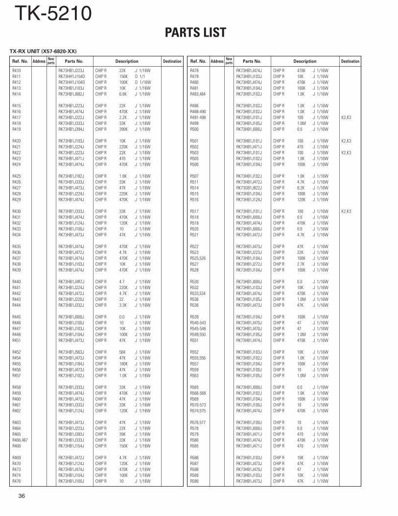
TK-5210PARTS LIST
36
Ref. No. Parts No. DescriptionAddressNewpartsRef. No. Parts No. DescriptionAddress
Newparts Destination Destination
TX-RX UNIT (X57-6820-XX)
R410 RK73HB1J223J CHIP R 22K J 1/16WR411 RK73HH1J154D CHIP R 150K D 1/1R412 RK73HH1J104D CHIP R 100K D 1/16WR413 RK73HB1J103J CHIP R 10K J 1/16WR414 RK73HB1J682J CHIP R 6.8K J 1/16W
R415 RK73HB1J223J CHIP R 22K J 1/16WR416 RK73HB1J474J CHIP R 470K J 1/16WR417 RK73HB1J222J CHIP R 2.2K J 1/16WR418 RK73HB1J333J CHIP R 33K J 1/16WR419 RK73HB1J394J CHIP R 390K J 1/16W
R420 RK73HB1J103J CHIP R 10K J 1/16WR421 RK73HB1J224J CHIP R 220K J 1/16WR422 RK73HB1J223J CHIP R 22K J 1/16WR423 RK73HB1J471J CHIP R 470 J 1/16WR424 RK73HB1J474J CHIP R 470K J 1/16W
R425 RK73HB1J182J CHIP R 1.8K J 1/16WR426 RK73HB1J333J CHIP R 33K J 1/16WR427 RK73HB1J473J CHIP R 47K J 1/16WR428 RK73HB1J224J CHIP R 220K J 1/16WR429 RK73HB1J474J CHIP R 470K J 1/16W
R430 RK73HB1J333J CHIP R 33K J 1/16WR431 RK73HB1J474J CHIP R 470K J 1/16WR432 RK73HB1J124J CHIP R 120K J 1/16WR433 RK73HB1J100J CHIP R 10 J 1/16WR434 RK73HB1J473J CHIP R 47K J 1/16W
R435 RK73HB1J474J CHIP R 470K J 1/16WR436 RK73HB1J472J CHIP R 4.7K J 1/16WR437 RK73HB1J474J CHIP R 470K J 1/16WR438 RK73HB1J103J CHIP R 10K J 1/16WR439 RK73HB1J474J CHIP R 470K J 1/16W
R440 RK73HB1J4R7J CHIP R 4.7 J 1/16WR441 RK73HB1J224J CHIP R 220K J 1/16WR442 RK73HB1J472J CHIP R 4.7K J 1/16WR443 RK73HB1J220J CHIP R 22 J 1/16WR444 RK73HB1J332J CHIP R 3.3K J 1/16W
R445 RK73HB1J000J CHIP R 0.0 J 1/16WR446 RK73HB1J100J CHIP R 10 J 1/16WR447 RK73HB1J103J CHIP R 10K J 1/16WR448 RK73HB1J104J CHIP R 100K J 1/16WR451 RK73HB1J473J CHIP R 47K J 1/16W
R452 RK73HB1J563J CHIP R 56K J 1/16WR454 RK73HB1J473J CHIP R 47K J 1/16WR455 RK73HB1J184J CHIP R 180K J 1/16WR456 RK73HB1J473J CHIP R 47K J 1/16WR457 RK73HB1J102J CHIP R 1.0K J 1/16W
R458 RK73HB1J333J CHIP R 33K J 1/16WR459 RK73HB1J474J CHIP R 470K J 1/16WR460 RK73HB1J473J CHIP R 47K J 1/16WR461 RK73HB1J333J CHIP R 33K J 1/16WR462 RK73HB1J124J CHIP R 120K J 1/16W
R463 RK73HB1J473J CHIP R 47K J 1/16WR464 RK73HB1J223J CHIP R 22K J 1/16WR465 RK73HB1J393J CHIP R 39K J 1/16WR466,467 RK73HB1J333J CHIP R 33K J 1/16WR468 RK73HB1J154J CHIP R 150K J 1/16W
R469 RK73HB1J472J CHIP R 4.7K J 1/16WR470 RK73HB1J124J CHIP R 120K J 1/16WR473 RK73HB1J474J CHIP R 470K J 1/16WR474 RK73HB1J104J CHIP R 100K J 1/16WR476 RK73HB1J100J CHIP R 10 J 1/16W
R478 RK73HB1J474J CHIP R 470K J 1/16WR479 RK73HB1J103J CHIP R 10K J 1/16WR480 RK73HB1J474J CHIP R 470K J 1/16WR481 RK73HB1J104J CHIP R 100K J 1/16WR483,484 RK73HB1J102J CHIP R 1.0K J 1/16W
R486 RK73HB1J102J CHIP R 1.0K J 1/16WR488-490 RK73HB1J102J CHIP R 1.0K J 1/16WR491-498 RK73HB1J101J CHIP R 100 J 1/16W K2,K3R499 RK73HB1J105J CHIP R 1.0M J 1/16WR500 RK73HB1J000J CHIP R 0.0 J 1/16W
R501 RK73HB1J101J CHIP R 100 J 1/16W K2,K3R502 RK73HB1J471J CHIP R 470 J 1/16WR503 RK73HB1J101J CHIP R 100 J 1/16W K2,K3R505 RK73HB1J102J CHIP R 1.0K J 1/16WR506 RK73HB1J104J CHIP R 100K J 1/16W
R507 RK73HB1J102J CHIP R 1.0K J 1/16WR511 RK73HB1J472J CHIP R 4.7K J 1/16WR514 RK73GB1J822J CHIP R 8.2K J 1/16WR515 RK73HB1J104J CHIP R 100K J 1/16WR516 RK73HB1J124J CHIP R 120K J 1/16W
R517 RK73HB1J101J CHIP R 100 J 1/16W K2,K3R518 RK73HB1J000J CHIP R 0.0 J 1/16WR519 RK73HB1J474J CHIP R 470K J 1/16WR520 RK73HB1J000J CHIP R 0.0 J 1/16WR521 RK73HB1J472J CHIP R 4.7K J 1/16W
R522 RK73HB1J473J CHIP R 47K J 1/16WR523 RK73HB1J223J CHIP R 22K J 1/16WR525,526 RK73HB1J104J CHIP R 100K J 1/16WR527 RK73HB1J272J CHIP R 2.7K J 1/16WR528 RK73HB1J104J CHIP R 100K J 1/16W
R530 RK73HB1J000J CHIP R 0.0 J 1/16WR532 RK73HB1J103J CHIP R 10K J 1/16WR533,534 RK73HB1J474J CHIP R 470K J 1/16WR536 RK73HB1J105J CHIP R 1.0M J 1/16WR538 RK73HB1J473J CHIP R 47K J 1/16W
R539 RK73HB1J104J CHIP R 100K J 1/16WR540-543 RK73HB1J470J CHIP R 47 J 1/16WR545-548 RK73HB1J470J CHIP R 47 J 1/16WR549,550 RK73HB1J105J CHIP R 1.0M J 1/16WR551 RK73HB1J474J CHIP R 470K J 1/16W
R552 RK73HB1J103J CHIP R 10K J 1/16WR555,556 RK73HB1J102J CHIP R 1.0K J 1/16WR557 RK73HB1J104J CHIP R 100K J 1/16WR559 RK73HB1J100J CHIP R 10 J 1/16WR563 RK73HB1J105J CHIP R 1.0M J 1/16W
R565 RK73HB1J000J CHIP R 0.0 J 1/16WR566-568 RK73HB1J102J CHIP R 1.0K J 1/16WR569 RK73HB1J104J CHIP R 100K J 1/16WR570-573 RK73HB1J100J CHIP R 10 J 1/16WR574,575 RK73HB1J474J CHIP R 470K J 1/16W
R576,577 RK73HB1J100J CHIP R 10 J 1/16WR578 RK73HB1J000J CHIP R 0.0 J 1/16WR579 RK73HB1J471J CHIP R 470 J 1/16WR580 RK73HB1J474J CHIP R 470K J 1/16WR585 RK73HB1J471J CHIP R 470 J 1/16W
R586 RK73HB1J103J CHIP R 10K J 1/16WR587 RK73HB1J473J CHIP R 47K J 1/16WR588 RK73HB1J470J CHIP R 47 J 1/16WR589 RK73HB1J103J CHIP R 10K J 1/16WR590 RK73HB1J473J CHIP R 47K J 1/16W

TK-5210PARTS LIST
Ref. No. Parts No. DescriptionAddressNewpartsRef. No. Parts No. DescriptionAddress
Newparts Destination Destination
TX-RX UNIT (X57-6820-XX)
37
R591 RK73HB1J470J CHIP R 47 J 1/16WR592 RK73HB1J000J CHIP R 0.0 J 1/16WR594,595 RK73HB1J104J CHIP R 100K J 1/16WR596 RK73HB1J103J CHIP R 10K J 1/16WR602 RK73HB1J104J CHIP R 100K J 1/16W
R603 RK73HB1J470J CHIP R 47 J 1/16WR604 RK73HB1J272J CHIP R 2.7K J 1/16WR605 RK73HB1J333J CHIP R 33K J 1/16WR606 RK73HB1J102J CHIP R 1.0K J 1/16WR607 RK73HB1J331J CHIP R 330 J 1/16W
R608 RK73HB1J102J CHIP R 1.0K J 1/16WR609 RK73HB1J104J CHIP R 100K J 1/16WR612 RK73HB1J154J CHIP R 150K J 1/16WR613 RK73HB1J184J CHIP R 180K J 1/16WR614 RK73HB1J223J CHIP R 22K J 1/16W
R616 RK73HB1J102J CHIP R 1.0K J 1/16WR617 RK73HB1J154J CHIP R 150K J 1/16WR618 RK73HB1J470J CHIP R 47 J 1/16WR619 RK73HB1J273J CHIP R 27K J 1/16WR620,621 RK73HB1J223J CHIP R 22K J 1/16W
R622 RK73HB1J473J CHIP R 47K J 1/16WR623 RK73HB1J223J CHIP R 22K J 1/16WR624 RK73HB1J182J CHIP R 1.8K J 1/16WR626 RK73HB1J182J CHIP R 1.8K J 1/16WR627,628 RK73HB1J473J CHIP R 47K J 1/16W
R631 RK73HB1J122J CHIP R 1.2K J 1/16WR634,635 RK73HB1J105J CHIP R 1.0M J 1/16WR637 RK73HB1J470J CHIP R 47 J 1/16WR638 RK73HB1J222J CHIP R 2.2K J 1/16WR640 RK73HB1J684J CHIP R 680K J 1/16W
R641 RK73HB1J105J CHIP R 1.0M J 1/16WR643 RK73HB1J105J CHIP R 1.0M J 1/16WR651 RK73HB1J000J CHIP R 0.0 J 1/16WR701-704 RK73HB1J102J CHIP R 1.0K J 1/16W K2R701-716 RK73HB1J102J CHIP R 1.0K J 1/16W K3
R717,718 RK73HB1J474J CHIP R 470K J 1/16WR719,720 RK73HB1J101J CHIP R 100 J 1/16W K2,K3R721 RK73HB1J181J CHIP R 180 J 1/16W K2,K3R722 RK73HB1J101J CHIP R 100 J 1/16W K3R723 RK73HB1J181J CHIP R 180 J 1/16W K2,K3
R724 RK73HB1J101J CHIP R 100 J 1/16W K3R727 RK73HB1J102J CHIP R 1.0K J 1/16WR728-730 RK73HB1J474J CHIP R 470K J 1/16WR731-733 RK73HB1J102J CHIP R 1.0K J 1/16W KR731-735 RK73HB1J102J CHIP R 1.0K J 1/16W K2,K3
R735 RK73HB1J102J CHIP R 1.0K J 1/16W KR736 RK73HB1J471J CHIP R 470 J 1/16WR737 RK73HB1J474J CHIP R 470K J 1/16WR738 RK73HB1J471J CHIP R 470 J 1/16WR739 RK73HB1J474J CHIP R 470K J 1/16W K2,K3
R740 RK73HB1J222J CHIP R 2.2K J 1/16W K2,K3R741-745 RK73HB1J102J CHIP R 1.0K J 1/16WR747 RK73HB1J102J CHIP R 1.0K J 1/16WR754 RK73HB1J474J CHIP R 470K J 1/16W K2,K3R756 RK73HB1J181J CHIP R 180 J 1/16W K2,K3
R760-762 RK73HB1J102J CHIP R 1.0K J 1/16W K2,K3R760,761 RK73HB1J102J CHIP R 1.0K J 1/16W KR763 RK73GJ1J333D CHIP R 33K D 1/16W K2,K3R764 RK73GH2A104D CHIP R 100K D 1/10W K2,K3R766 RK73HB1J223J CHIP R 22K J 1/16W K2,K3
R767 RK73HH1J223D CHIP R 22K D 1/16W K2,K3R768 RK73HB1J223J CHIP R 22K J 1/16W K2,K3R770 RK73GB2A000J CHIP R 0.0 J 1/10W K2,K3R803 RK73GB1J2R2J CHIP R 2.2 J 1/16WR804 RK73HB1J000J CHIP R 0.0 J 1/16W
R805,806 RK73GB1J2R2J CHIP R 2.2 J 1/16WR807 RK73HB1J000J CHIP R 0.0 J 1/16WR808 RK73GB1J4R7J CHIP R 4.7 J 1/16WR812 RK73GB1J100J CHIP R 10 J 1/16WR813 RK73HB1J000J CHIP R 0.0 J 1/16W
R814 RK73GB2A000J CHIP R 0.0 J 1/10WR815 RK73HB1J103J CHIP R 10K J 1/16WR817 RK73HB1J224J CHIP R 220K J 1/16WR818 RK73HB1J334J CHIP R 330K J 1/16WR819 RK73HB1J124J CHIP R 120K J 1/16W
R825 RK73HB1J154J CHIP R 150K J 1/16WR826 RK73HB1J123J CHIP R 12K J 1/16WR827 RK73HH1J334D CHIP R 330K D 1/16WR828 RK73HH1J223D CHIP R 22K D 1/16WR832 RK73HB1J330J CHIP R 33 J 1/16W
R850 RK73HB1J102J CHIP R 1.0K J 1/16WR900-903 RK73HB1J101J CHIP R 100 J 1/16WR904 RK73HB1J000J CHIP R 0.0 J 1/16WR905 RK73HB1J332J CHIP R 3.3K J 1/16WR906 RK73HB1J104J CHIP R 100K J 1/16W
R907 RK73HB1J100J CHIP R 10 J 1/16WR909 RK73GB2A000J CHIP R 0.0 J 1/10WR910 RK73HB1J000J CHIP R 0.0 J 1/16WR950 RK73HB1J821J CHIP R 820 J 1/16WR951 RK73HB1J103J CHIP R 10K J 1/16W
R952 RK73HB1J000J CHIP R 0.0 J 1/16W
S901 S64-0406-05 LEVER SWITCHS902 S70-0496-05 TACT SWITCH
D1 MA2S111-F DIODED2 ,3 NNCD6.8G ZENER DIODED4 ,5 AVRM1005C270M VARISTORD13 ,14 1SS388 DIODED101 HVC131 DIODE
D105 HZU5CLL ZENER DIODED106-109 HVC131 DIODED110,111 EZJZ0V500AA VARISTORD202-209 1SV273 VARIABLE CAPACITANCE DIODED210 HVC131 DIODE
D303,304 HVC376B VARIABLE CAPACITANCE DIODED306-311 ∗ 1SV282-F VARIABLE CAPACITANCE DIODED312 1SV278 VARIABLE CAPACITANCE DIODED313 MA2S111-F DIODED314 DA221 DIODE
D401 1SR154-400 DIODED402-404 RB706F-40 DIODED405 1SS388 DIODED604 NNCD6.8G ZENER DIODED608,609 1SS388 DIODE
D701-704 IMN10 DIODE K3D701,702 IMN10 DIODE K2D717-719 IMN10 DIODE K3D718,719 IMN10 DIODE K,K2D720 UDZS3.9B ZENER DIODE K2,K3

TK-5210PARTS LIST
38
Ref. No. Parts No. DescriptionAddressNewpartsRef. No. Parts No. DescriptionAddress
Newparts Destination Destination
TX-RX UNIT (X57-6820-XX)
D801 1SS301 DIODED802 HRB0502A DIODED803,804 DA221 DIODED805 CUS01 DIODED850 MA2S111-F DIODE
IC1 RV5C386A MOS-ICIC2 AT2425610TI27 ROM ICIC3 ∗ S-80930CNNB-G MOS-ICIC4 MM1522XURE ANALOGUE ICIC5 ∗ 30625MGP346HU MICROPROCESSOR IC
IC6 Note 1 ROM ICIC7 TC7S08FU MOS-ICIC8 Note 1 MICROPROCESSOR ICIC9 TC74VHCT244AFT MOS-ICIC10 TC7W53FK HYBRID IC
IC11 BU4094BCFV MOS-ICIC12 TC7WH74FK MOS-ICIC13 ∗ EX128TQ64I630C MOS-ICIC14 TC7WU04FK MOS-ICIC101 TA75W01FU MOS-IC
IC102,103 ∗ MASWSS0181 ANALOGUE ICIC104 TC75W51FK MOS-ICIC201 LMC7101BIM5 MOS-ICIC202 SPM5001 MOS-ICIC203 TC7W53FK HYBRID IC
IC204 TA31137FN MOS-ICIC205-207 TC7W53FK HYBRID ICIC208 TC7WU04FK MOS-ICIC301 LMC7101BIM5 MOS-ICIC303 ADF4111BCP7 MOS-IC
IC304 UPB1511TB BI-POLAR ICIC401 XC6204B502PR MOS-ICIC402 XC6204B502MR MOS-ICIC403 TC75W51FK MOS-ICIC404 TC7W66FK MOS-IC
IC405 TC75W51FK MOS-ICIC406 AK4550VTP MOS-ICIC407 TC75W51FK MOS-ICIC408 TC7W66FK MOS-ICIC409 TC75W51FK MOS-IC
IC411 M62364FP-F MOS-ICIC412 TC75W51FK MOS-ICIC413 TC7W66FK MOS-ICIC414 MCP41100T ANALOGUE ICIC415 TC7MB3245FK MOS-IC
IC416,417 TC7WB125FK MOS-ICIC418 TC75S51FE MOS-ICIC501,502 TC7SBD384AFU MOS-ICIC520 TK11250CUCB MOS-ICIC601,602 LM4906LD ANALOGUE IC
IC603 TC75W51FK MOS-ICIC604 TC7W66FK MOS-ICIC606 XC6201P302MR MOS-ICIC701-703 BU4094BCF MOS-ICIC704 LMC7101BIM5 MOS-IC K2,K3
IC801,802 XC6204B332M MOS-ICIC803 XC6209B152M MOS-ICIC804 XC61CC5602NR MOS-ICIC805 XC6365D103M MOS-ICIC806 XC6204B252M MOS-IC
IC807 TK11250CUCB MOS-ICIC808 XC9101D09AKR ANALOGUE IC
Q1 UM6K1N FETQ101 2SC5108(Y) TRANSISTORQ102 2SC5192-A TRANSISTORQ103 RD01MUS1 FETQ104 SSM3K15TE FET
Q105 RD07MVS1 FETQ106 DTA144EE DIGITAL TRANSISTORQ107 SSM3K15TE FETQ110 2SJ243 FETQ111 EMD9 TRANSISTOR
Q201 2SC4617(S) TRANSISTORQ202 3SK274∗J FETQ204 2SK1215(E) FETQ205 2SC5108(Y) TRANSISTORQ209 EMD9 TRANSISTOR
Q306 2SK879(GR,Y) FETQ307 2SC4617(S) TRANSISTORQ308 SSM6L05FU FETQ309 2SJ347 FETQ310,311 2SK508NV(K52) FET
Q312-314 2SC5108(Y) TRANSISTORQ315 2SC4617(S) TRANSISTORQ316 SSM6L05FU FETQ401,402 SSM6L05FU FETQ403 TPC6102 FET
Q404 2SC4738(GR) TRANSISTORQ405 2SA1832(GR) TRANSISTORQ406 SSM3K15TE FETQ407 2SJ347 FETQ408,409 SSM3K15TE FET
Q410 2SJ347 FETQ411 SSM3K15TE FETQ412 2SC4617(S) TRANSISTORQ413 SSM3K15TE FETQ415 SSM6L05FU FET
Q416-418 SSM3K15TE FETQ420 SSM6L05FU FETQ520 UM6K1N FETQ601 SSM3K15TE FETQ605 UMG3N TRANSISTOR
Q606 SSM3K15TE FETQ607 UMC4N TRANSISTORQ608 2SB798(DL,DK) TRANSISTORQ609 2SJ243 FETQ610 SSM3K15TE FET
Q611 2SJ243 FETQ612 SSM3K15TE FETQ702 SSM3K15TE FETQ703,704 SSM6L05FU FETQ705 2SC4617(S) TRANSISTOR K2,K3
Q706 2SB798(DL,DK) TRANSISTOR K2,K3Q801 TPC6102 FETQ802 SSM5H01TU FET
TH101 B57331V2104J THERMISTOR
Note 1 : This part cannot be replaced. Therefore, this part is not supplied as a service part.

39
TK-5210
A B
1
2
3
CF202
XF201
88
39Px2
Px2
Px2
Px2
P
Px3
PP
P
Px2 Px2
Px2
P
8713
1
41
Control PCB(X57 B/5)
97
51
29
42
4172
4
28
12
6
53
32x2
26
90
91
69
5527
54
30
F
20
Dx2Dx2
Cx2
Cx2
34
71
96
74
9450
23
7362 40
43
63
46x2
45
48
66
47
8567 7
964
68
59 1480
5
60
52
24
31
75
49
93
50
9470
86
8384
61
B
K
N Q
A
Ex2
B
H
IJ
700
701
35 8
74 Top PCB(X57 C/5)
ANT PCB (X57 E/5)
TX-RX PCB(X57 A/5)
Option PCB(X57 D/5)
EXPLODED VIEW (TK-5210 K)
Parts with the exploded numbers larger than 700 are not supplied.
A :N08-0531-14B :N09-2439-25C :N09-2440-15D :N09-2441-15E :N09-2442-15
F :N09-2443-14H :N14-0813-14I :N14-0814-14J :N14-0815-04K :N14-0817-14
M :N30-3008-60N :N32-2004-48P :N83-2005-48Q :N83-2006-43
Note: If a part reference number is listed in a box on the
exploded view of the PCB, that part does not come
with the PCB. These parts must be ordered
separately.
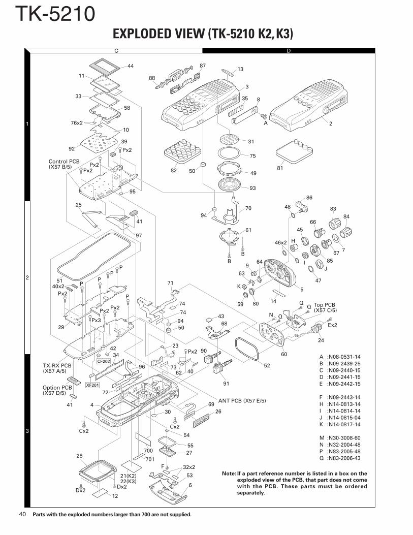
40
TK-5210
C D
1
2
3
CF202
XF201
39
58
44
10
11
33
92
76x2
Px2
Px2Px2
Px2
P
Px3
PP
P
Px2 Px2
Px2
P
40x2
82 81
A 2
3
41
97
Control PCB(X57 B/5)
51
29
4
28
12
26
90
91
6930
21(K2)22(K3)
Dx2Dx2
Cx2Cx2
34
71
96
74
9450
23
7362 40
43
63
46x2
45
48
66
47
8567 7
964
68
59 1480
5
60
52
24
31
75
49
93
50
9470
86
8384
61
B
K
N Q
Ex2
B
H
IJ
95
25
88
8713
35 8
74
700
701
72
TX-RX PCB(X57 A/5)
Option PCB(X57 D/5)
ANT PCB (X57 E/5)41
Top PCB(X57 C/5)
6
53
32x2
5527
54
F
42
EXPLODED VIEW (TK-5210 K2,K3)
Parts with the exploded numbers larger than 700 are not supplied.
A :N08-0531-14B :N09-2439-25C :N09-2440-15D :N09-2441-15E :N09-2442-15
F :N09-2443-14H :N14-0813-14I :N14-0814-14J :N14-0815-04K :N14-0817-14
M :N30-3008-60N :N32-2004-48P :N83-2005-48Q :N83-2006-43
Note: If a part reference number is listed in a box on the
exploded view of the PCB, that part does not come
with the PCB. These parts must be ordered
separately.
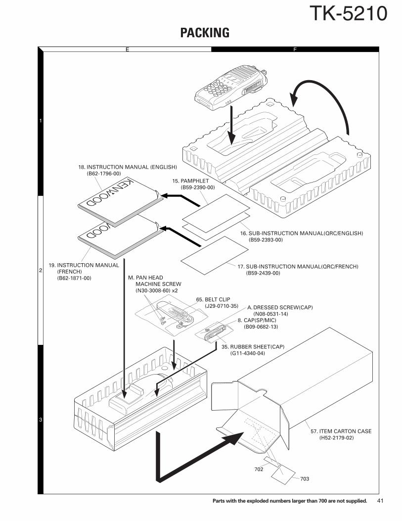
41
TK-5210PACKING
E F
1
2
3
Parts with the exploded numbers larger than 700 are not supplied.
18. INSTRUCTION MANUAL (ENGLISH)(B62-1796-00)
19. INSTRUCTION MANUAL(FRENCH)(B62-1871-00)
16. SUB-INSTRUCTION MANUAL(QRC/ENGLISH) (B59-2393-00)
15. PAMPHLET(B59-2390-00)
17. SUB-INSTRUCTION MANUAL(QRC/FRENCH)(B59-2439-00)
8. CAP(SP/MIC)(B09-0682-13)
A.DRESSED SCREW(CAP)(N08-0531-14)
M. PAN HEAD MACHINE SCREW (N30-3008-60) x2
702
703
35. RUBBER SHEET(CAP)(G11-4340-04)
65. BELT CLIP(J29-0710-35)
57. ITEM CARTON CASE(H52-2179-02)

TK-5210
42
• Key operation
Key Function Display
[Selector] Test frequency channel up/down Channel No.
[Concentric switch] Channel spacing switching Wide :"W"
(Position "A":Wide, Narrow :"N"Position "B":Narrow, P25 :"A"
Position "C":P25)
[Lever switch] RF output power switching Low power :"LO"
(_:Low power, -:High power) High power :"HI"
[PTT] Transmit -
[Side1] Squelch level change Squelch level 0:"SQ.LV0"(0t1t2t • • • t9t0t1t2t • • • ) Squelch level 1:"SQ.LV1"
Squelch level 9:"SQ.LV9"
[Side1] Hold Squelch off
[Side2] MSK baud rate change 2400bps: icon
(1200bps/2400bps) appears
[Side2] Hold Compander on/off On: icon appears
[Side3] Shifts to the Panel tuning mode -
[Side3] Hold LCD all lights LCD all point appears
[Orange] Beat shift on/off On: icon appears
[A] Unused -
[B] Unused -
[C] Test signaling down Signaling No.
[D] Test signaling up Signaling No.
[0] to [9] and Use as the DTMF keypad. -[#], [*] If a key is pressed during transmission,
the DTMF corresponding to the
key that was presses is sent.
• LED indicatorRed LED Lights during transmission. Blinks at the low
battery voltage warning.Green LED Lights when there is carrier.
• LCD display in the panel test mode
• Filter Mode
Display Condition Key
W WIDE (25kHz) Filter Concentric switch "A"
N NARROW (12.5kHz) Filter Concentric switch "B"
A P25 (12.5kHz) Filter Concentric switch "C"
ADJUSTMENT
A B
C
6
MIC
Volume
Selector
Side 1 key
Side 2 key
PTT switch
Concentric Switch
Lever switchOrange key
Universalconnector
Side 3 key
Controls
Panel Test Mode (K2 and K3 models only)
For the K model (without LCD), perform "Test mode" usingthe KPG-95D.
Test mode operation featuresThis transceiver has a test mode. To enter panel test
mode, press and hold the [Side3] and [PTT] keys whileturning the transceiver power on and then the [PTT] keyfirst. Test mode can be inhibited by programming. To exittest mode, switch the power on again.
• When the panel test mode is activated, the channel se-lected with the [Selector] knob and the last used signalingnumber are displayed. When it is activated for the firsttime, the signaling number is 1.
• If test signaling 20 (Tone Test Pattern) is selected, the re-sult of Bit Error Rate (BER) calculation is displayed on theLCD. The BER value is also output from the serial port.
• The P25 and analog modes are switched automatically byselecting test signaling. When P25 mode is effective, “A”is displayed on the LCD.
LOW
1-1 [ None ]SQ.LV1
Channel No. Signaling No.
W: WideN : NarrowA : P25
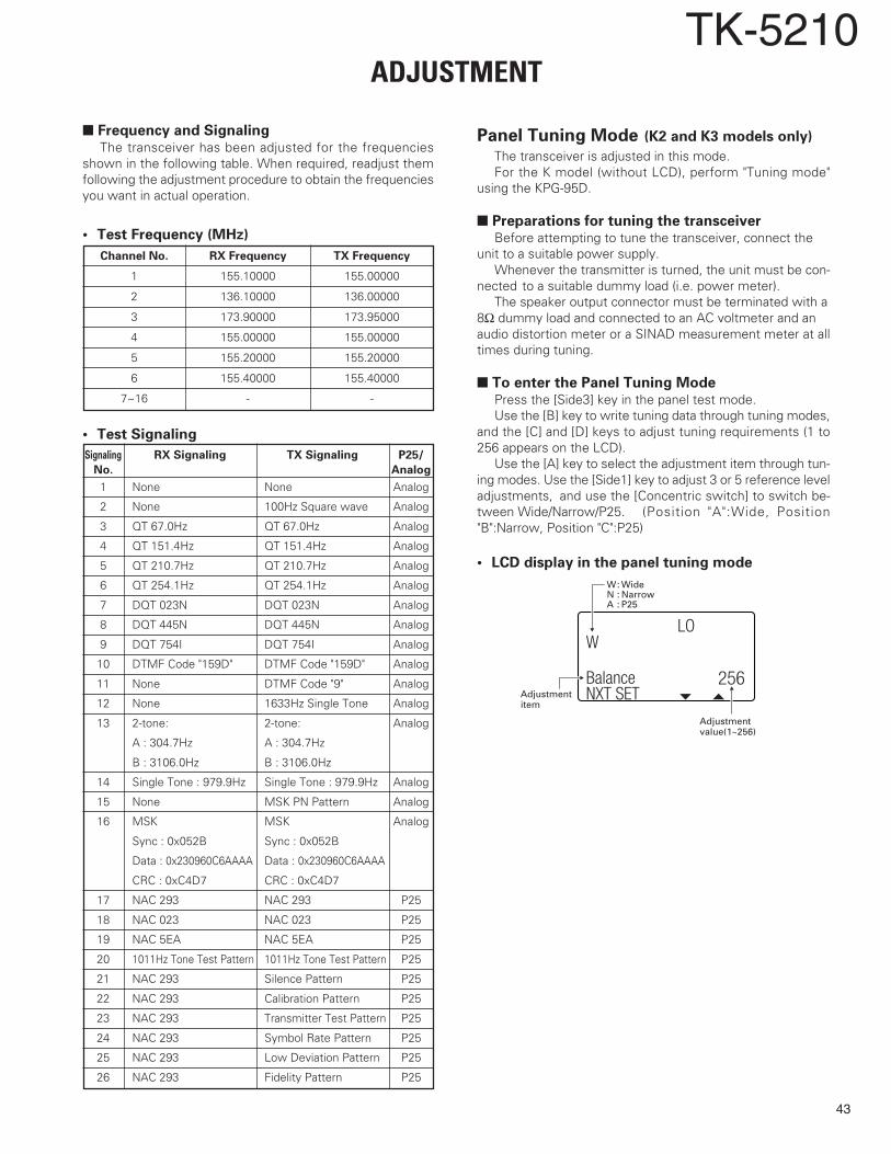
TK-5210
43
ADJUSTMENT
Panel Tuning Mode (K2 and K3 models only)
The transceiver is adjusted in this mode.For the K model (without LCD), perform "Tuning mode"
using the KPG-95D.
Preparations for tuning the transceiverBefore attempting to tune the transceiver, connect the
unit to a suitable power supply.Whenever the transmitter is turned, the unit must be con-
nected to a suitable dummy load (i.e. power meter).The speaker output connector must be terminated with a
8Ω dummy load and connected to an AC voltmeter and anaudio distortion meter or a SINAD measurement meter at alltimes during tuning.
To enter the Panel Tuning ModePress the [Side3] key in the panel test mode.Use the [B] key to write tuning data through tuning modes,
and the [C] and [D] keys to adjust tuning requirements (1 to256 appears on the LCD).
Use the [A] key to select the adjustment item through tun-ing modes. Use the [Side1] key to adjust 3 or 5 reference leveladjustments, and use the [Concentric switch] to switch be-tween Wide/Narrow/P25. (Position "A":Wide, Position"B":Narrow, Position "C":P25)
• LCD display in the panel tuning mode
Frequency and SignalingThe transceiver has been adjusted for the frequencies
shown in the following table. When required, readjust themfollowing the adjustment procedure to obtain the frequenciesyou want in actual operation.
• Test Frequency (MHz)
Channel No. RX Frequency TX Frequency
1 155.10000 155.00000
2 136.10000 136.00000
3 173.90000 173.95000
4 155.00000 155.00000
5 155.20000 155.20000
6 155.40000 155.40000
7~16 - -
• Test Signaling
Signaling RX Signaling TX Signaling P25/
No. Analog
1 None None Analog
2 None 100Hz Square wave Analog
3 QT 67.0Hz QT 67.0Hz Analog
4 QT 151.4Hz QT 151.4Hz Analog
5 QT 210.7Hz QT 210.7Hz Analog
6 QT 254.1Hz QT 254.1Hz Analog
7 DQT 023N DQT 023N Analog
8 DQT 445N DQT 445N Analog
9 DQT 754I DQT 754I Analog
10 DTMF Code "159D" DTMF Code "159D" Analog
11 None DTMF Code "9" Analog
12 None 1633Hz Single Tone Analog
13 2-tone: 2-tone: Analog
A : 304.7Hz A : 304.7Hz
B : 3106.0Hz B : 3106.0Hz
14 Single Tone : 979.9Hz Single Tone : 979.9Hz Analog
15 None MSK PN Pattern Analog
16 MSK MSK Analog
Sync : 0x052B Sync : 0x052B
Data : 0x230960C6AAAA Data : 0x230960C6AAAA
CRC : 0xC4D7 CRC : 0xC4D7
17 NAC 293 NAC 293 P25
18 NAC 023 NAC 023 P25
19 NAC 5EA NAC 5EA P25
20 1011Hz Tone Test Pattern 1011Hz Tone Test Pattern P25
21 NAC 293 Silence Pattern P25
22 NAC 293 Calibration Pattern P25
23 NAC 293 Transmitter Test Pattern P25
24 NAC 293 Symbol Rate Pattern P25
25 NAC 293 Low Deviation Pattern P25
26 NAC 293 Fidelity Pattern P25
LOW
NXT SETBalance 256
Adjustmentvalue(1~256)
Adjustmentitem
W: WideN : NarrowA : P25

TK-5210
44
• 3 or 5 reference level adjustments frequency
Tuning point Display RX (MHz) TX (MHz)
Low L 136.10000 136.00000
Low' LC 145.60000 145.50000
Center C 155.10000 155.00000
High CH 164.60000 164.50000
High ' H 173.90000 173.95000
ADJUSTMENT
• Key operation
Key Function
[Selector] Unused
[Concentric switch] Channel spacing switching (Position "A": Wide,
Position "B": Narrow, Position "C": P25)
[Lever switch] Unused
[PTT] Transmission. When the battery low voltage is
adjusted, the adjustment value is displayed on the LCD.
[Side1] To enter 3 or 5 reference level adjustments
[Side2] Unused
[Side3] Exit the panel tuning mode and shift to the
panel test mode.
[Orange] Unused
[A] Go to the next adjustment item
(The current adjustment data is cleared.)
[A] Hold Back to the last adjustment item
(The current adjustment data is cleared.)
[B] Write the new adjustment value to the transceiver.
[C] Adjustment value down
[D] Adjustment value up
• Adjustment item and Display (***: 1~256)
No. Adjustment item Display Wide/Narrow/P25 Tuning point Note
1 RX assist voltage RX V Assist *** - 5
2 TX assist voltage TX V Assist *** - 5
3 RX front-end RX Front-end *** - 5 AF unmute
4 2nd local frequency 2nd Lo Freq *** - 1
5 Frequency Frequency *** - 1
6 High power High Power *** - 5
7 Low power Low Power *** - 3
8 Mic sensitivity Mic Sense *** - 1
9 Balance Balance *** Wide/Narrow/P25 W:5/N:1/A:1 100Hz Square Wave
10 FM maximum deviation FM Max Dev *** Wide/Narrow W:5/N:1
11 P25 High deviation APCO Hi Dev *** P25 A:5 Symbol Rate Pattern
12 QT deviation QT Dev *** Wide/Narrow W:5/N:1 QT : 67Hz
13 DQT deviation DQT Dev *** Wide/Narrow W:5/N:1 DQT : 023N
14 DTMF deviation DTMF Dev *** Wide/Narrow W:1/N:1 DTMF Code : 9
15 Single tone deviation Tone Dev *** Wide/Narrow W:1/N:1 Single Tone : 1633Hz
16 MSK deviation MSK Dev *** Wide/Narrow W:1/N:1 MSK PN Pattern
17 Squelch (Threshold:1) Squelch (1) *** Wide/Narrow W:3/N:1 AF unmute
18 Squelch (Tight:9) Squelch (9) *** Wide/Narrow W:3/N:1 AF unmute
19 RSSI (Reference) RSSI (Ref) *** - 3
20 RSSI (-120dBm) RSSI (-120) *** - 3
21 RSSI (-70dBm) RSSI (-70) *** - 3
22 Battery TX inhibit voltage Battery *** - 1

TK-5210
45
ADJUSTMENTADJUSTMENT
Flow Chart
RX V Assist
[A]
[Side 1] 5 reference leveladjustments
[Side 1] 5 reference leveladjustments
[Side 1] 5 reference leveladjustments
[Side 1] 5 reference leveladjustments
[Side 1] 5 reference leveladjustments
[Side 1] 3 reference leveladjustments
[Side 1] 3 reference leveladjustments
[Side 1] 3 reference leveladjustments
[Side 1] 3 reference leveladjustments
[Side 1] 5 reference leveladjustments
[Side 1] 3 reference leveladjustments
[Side 1] 3 reference leveladjustments
[Side 1] 5 reference leveladjustments
[Side 1] 5 reference leveladjustments
[Side 1] 5 reference leveladjustments
Panel Test Mode
(Panel Tuning Mode)
[Side 3][Side 3]
TX V Assist
[A]
[Concentric SW]B
[Concentric SW]B [Concentric SW]C
[Concentric SW]B C
[Concentric SW]A
[Concentric SW]A
[Concentric SW]A
[Concentric SW]B,C[Concentric SW]A
[Concentric SW]C
RX Front-end
[A]
2nd Lo Freq
[A]
Frequency
[A]
High Power
[A]
APCO Hi Dev
[A]
[A] [A] [A]
Low Power
[A]
[Side 1]5 reference leveladjustments
5 reference leveladjustments exit
[Side 1]
L
LC
H[Side 1]
[Side 1]C
[Side 1]CH
Low
Low'
High
Center
High'
[A]
[A]
[A]
[A]
[A]
[Side 1]3 reference leveladjustments
3 reference leveladjustments exit
L
H[Side 1]
[Side 1]C
Low
High
Center
[A]
[A]
[A]
Mic Sense
[A]
RSSI(Ref)
[A]
[A]
Balance Wide Balance Narrow
[A] [A]
FM Max Dev Wide FM Max Dev Narrow
[Concentric SW]B,C
[A](Hold)
[Concentric SW]A
[Concentric SW]B,C[Concentric SW]A
[Concentric SW]A
[A] [A]
QT Dev Wide QT Dev Narrow
[Concentric SW]A
[Concentric SW]A
[A] [A]
DQT Dev Wide DQT Dev Narrow
[A] [A]
DTMF Dev Wide DTMF Dev Narrow
[Concentric SW]A
[A] [A]
Tone Dev Wide Tone Dev Narrow
[Concentric SW]A
[A] [A]
MSK Dev Wide MSK Dev Narrow
[Concentric SW]A
[A]
Squelch(1) Wide Squelch(1) Narrow
[A]
[Concentric SW]B,C[Concentric SW]A
[Concentric SW]A
[A]
Squelch(9) Wide Squelch(9) Narrow
Balance P25
RSSI(-120)
[A]
RSSI(-70)
[A]
Battery
[A]
B
B,C
B,C
B,C
B,C
B,C
B,C
B,C
B,C

TK-5210
46
BER (Bit Error Rate) Measurement1. The Panel Test Mode is used to measure the BER (Refer
to "Test mode operation features" described on page 42.).2. Select ”20” for test signaling (Refer to "Test Signaling"
described on page 43.).When "20" is selected for the test signaling, the filter isautomatically selected to "P25".(If there is no RF input signal, the display shows”500000”)
3. Select a filter (Refer to "Filter Mode" described on page42.).
4. Select a test frequency (Refer to "Test Frequency" de-scribed on page 43.).
C4FM (P25) Deviation Adjustment1. The TK-5210 adjusts the deviation between High Devia-
tion ±1800Hz for the C4FM (P25).2. The Symbol Rate Pattern is used when adjusting the High
Deviation for the C4FM (P25) (Refer to "Test Signaling" de-scribed on page 43.). This test signal has a peak deviationequal to π/2 1800Hz = 2827Hz.
Service Jig
Nut wrenchIn order to turn the volume nut and the channel selector
nut, use a recommendation tool.KENWOOD part No. : W05-1123-00
5. Measure the BER (Bit Error Rate) using the digital radiotester. Enter a standard input signal into the transceiver asa standard tone test pattern.
6. Adjust the input signal level to achieve the standard biterror rate (BER).(For example, if the BER is 5%, the display shows”050000”.)
ADJUSTMENT
Adjustment Points
L201
L202
L204L205
S
RX BPF
+
TX-RX UNIT (A/5) : TX-RX section
Component side
S
2nd Lo
+
TX-RX UNIT (A/5) : TX-RX section
Foil side
BPF GND
RX BPF
CV

TK-5210
47
ADJUSTMENT
Test Equipment Required for AlignmentTest Equipment Major Specifications
1. Standard Signal Generator Frequency Range 136 to 174MHz(SSG) Modulation Frequency modulation and external modulation
Output -127dBm/0.1µV to greater than -47dBm/1mV2. Power Meter Input Impedance 50Ω
Operation Frequency 136 to 174MHzMeasurement Range Vicinity of 10W
3. Deviation Meter Frequency Range 136 to 174MHz4. Digital Volt Meter Measuring Range 10mV to 10V DC
(DVM) Input Impedance High input impedance for minimum circuit loading5. Oscilloscope DC through 30MHz6. High Sensitivity Frequency Range 10Hz to 1000MHz
Frequency Counter Frequency Stability 0.2ppm or less7. Ammeter 5A8. AF Volt Meter Frequency Range 50Hz to 10kHz
(AF VTVM) Voltage Range 1mV to 10V9. Audio Generator (AG) Frequency Range 50Hz to 5kHz or more
Output 0 to 1V10. Distortion Meter Capability 3% or less at 1kHz
Input Level 50mV to 10Vrms11. Spectrum Analyzer Measuring Range DC to 1GHz or more12. Tracking Generator Center frequency 50kHz to 600MHz
Output Voltage 100mV or more13. 8Ω Dummy Load Approx. 8Ω, 3W14. Regulated Power Supply 5V to 10V, approx. 3A
Useful if ammeter equipped
The following parts are required for
adjustment
1. Antenna connector adapter
The antenna connector of this transceiver uses an SMAterminal.
Use an antenna connector adapter [SMA(f) – BNC(f) orSMA(f) – N(f)] for adjustment. (The adapter is not provided asan option, so buy a commercially-available one.)
Note :
When the antenna connector adapter touches the knob,draw out the knob to mount the connector.
2. Universal connectorUse the interface cable (KPG-36/36A) for PC tuning or the
lead wire with plug (E30-3287-18) and screw (N08-0535-08)for panel tuning. Connect the plug to the universal connectorof the transceiver and tighten the screw.
The lead wire with plug (E30-3287-18) and screw (N08-0535-08) terminals are as follows. Numbers are universalconnector terminal numbers.
Caution1. When connecting the plug to the universal connector of
the transceiver, a short circuit may occur. To prevent this,be sure to turn the transceiver POWER switch off.
2. Since the RX AF output is a BTL output, there is a DCcomponent. Isolate this with a capacitor or transformer asshown in the figure.
3. Do not connect an instrument between red or black andGND.
• Universal connector
1 : SSW
3 : SP–
5 : EMC
7 : PTT
9 : OPT
11 : 5M
13 : RXD
2 : SP+
GNDEXT ANTGND
4 : MSW
6 : ME
8 : PF
10 : E
12 : TXD
14 : NC

TK-5210
48
ADJUSTMENTADJUSTMENT
• Panel tuning
• PC tuning
Connect the wires to the PCB in the connector case ofinterface cable.
For output the wires out of the connector case, need toprocess the connector case.
11 : GREEN (5M)
TUBE
SCREW
8 : YELLOW (PF SW)
2 : RED (RX AF OUTPUT)
3 : BLACK (RX AF OUTPUT)
10 : BROWN (GND)
6 : BROWN (MIC GND)
5 : WHITE (MIC INPUT)
7 : BLUE (PTT SW) GND → ON
RED (2)
BLK (3)
100µ 10V
100µ 10V
8Ω
WHT(5)
BRN (6)
BLU (7)
BRN (10)
PTT SW
+
+
+
To transceiver
AF Voltmeter
Audio generator10µ 10V
Connector case
KPG-36/36A
Remove thescrew
PCB layout
Shield
AF voltmeter
Audio generator
100µ 10V
100µ 10V
10µ 10V
+
+
+
8Ω
How to Remove the Flat Cable1. Gently draw out both sides of the connector lever uni-
formly in the direction of the arrow with tweezers.(CN7, CN19, CN604, CN751, CN752, CN753)CN19, CN604, CN751:K2 and K3 models only
2. Gently rise up the connector lever in the direction of thearrow with a flat-head screwdriver or tweezers.(CN603)
Note : Gently push both sides of the connector lever, whenput in the flat cable.
Tweezers
Flat cable
Lever
Flat-headscrewdriver
Flat cable
Lever
3. Gently depress the connector lever in the direction of thearrow with a flat-head screwdriver or tweezers.(CN902, CN903)
Lever
Flat cable
Flat-headscrewdriver

TK-5210
49
Common Section
Measurement Adjustment
Item Condition Test-Unit Terminal Unit Parts Method
Specifications/Remarksequipment
1. Setting 1) BATT terminal voltage:7.5V2) SSG standard modulation
[Wide] MOD:1kHz,DEV:3kHz[Narrow] MOD:1kHz,DEV:1.5kHz
2. Assist [Panel tuning mode] Power meter Panel ANT Panel [C],[D] Change the 1.88V±0.1Vvoltage 1) Adj item:[RX V Assist] DVM TX-RX CV adjustment value
Adjust:[***] (A/5) within the limit When adjusting the assist•RX 2) Adj item:[L RX V Assist]t of the specified voltage in PC tuning mode,
[LC RX V Assist]t[C RX V Assist]t voltage. slide the bar to indicate[CH RX V Assist]t[H RX V Assist] "VCO Lock Voltage" withinAdjust:[***] 2.0V±0.1V on Meter window.
Press [B] to store the adjustmentvalue after adjustment.
•TX 3) Adj item:[TX V Assist]Adjust:[***]
4) Adj item:[L TX V Assist]t[LC TX V Assist]t[C TX V Assist]t[CH TX V Assist]t[H TX V Assist]Adjust:[***]PTT:ON
Press [B] to store the adjustmentvalue after adjustment.
3. RX Front-end 1) Adj item:[RX Front-end] Spectrum Panel ANT TX-RX L201 After setting theadjust Adjust:[***] analyzer TX-RX RX BPF (A/5) adjustment value
2) Adj item:[L RX Front-end] Tracking (A/5) BPF GND to 245, adjust coilSpectrum analyzer setting generator to get the waveform
Center-f :136.1MHz as shown to theSpan :100MHz right.RBW :300kHzVBW :100kHzSWP :50msTG level :-30dBmXdB/div :10dB
Press [B] to store the adjustmentvalue after adjustment.3) Adj item:[H RX Front-end] L202 After setting the
Spectrum analyzer setting L204 adjustment valueCenter-f:173.9MHz L205 to 90, adjust each
Press [B] to store the adjustment coil to get thevalue after adjustment. highest peak points.
Furthermore, changethe adjustmentvalues to get thewaveform as shownto the right.
4) Adj item:[LC RX Front-end] Panel [C],[D] Change theSpectrum analyzer setting adjustment valuesCenter-f:145.6MHz to get the waveform
Press [B] to store the adjustment as shown to thevalue after adjustment. right.
ADJUSTMENT
REF 0.0 dBm
CENTER 136.1 MHz
RBW 300 kHzVBW 100 kHzSWP 50ms SPAN 100.0 MHz
10dB/A_Write Norm B_BlankATT 10dB
CENTER136.1 MHz
REF 0.0 dBm
CENTER 173.9 MHz
RBW 300 kHzVBW 100 kHzSWP 50ms SPAN 100.0 MHz
10dB/A_Write Norm B_BlankATT 10dB
CENTER173.9 MHz
REF 0.0 dBm
CENTER 145.6 MHz
RBW 300 kHzVBW 100 kHzSWP 50ms SPAN 100.0 MHz
10dB/A_Write Norm B_BlankATT 10dB
CENTER145.6 MHz

TK-5210
50
1. Frequency [Panel test mode] f.counter Panel ANT Panel [C],[D] Center frequency Note:After replacing theadjust 1) CH-Sig:3-1 ±50Hz VCXO(X201) align frequency.
[Panel tuning mode]
2) Adj item:[Frequency]Adjust:[***]PTT:ON
Press [B] to store the adjustmentvalue after adjustment.
2. High power 1) Adj item:[High Power] Power meter 4.8W +0.2W/-0.1Wadjust Adjust:[***] Ammeter 2.0A or less
2) Adj item:[L High Power]t[LC High Power]t[C High Power]t[CH High Power]t[H High Power]Adjust:[***]PTT:ON
Press [B] to store the adjustmentvalue after adjustment.
3. Low power 1) Adj item:[Low Power] 1.0W ±0.2Wadjust Adjust:[***] 1.4A or less
2) Adj item:[L Low Power]t[C Low Power]t[H Low Power]Adjust:[***]PTT:ON
Press [B] to store the adjustmentvalue after adjustment.
5) Adj item:[C RX Front-end] Spectrum Panel ANT Panel [C],[D] Change theSpectrum analyzer setting analyzer TX-RX RX BPF adjustment valuesCenter-f:155.1MHz (A/5) BPF GND to get the waveform
Press [B] to store the adjustment as shown to thevalue after adjustment. right.
6) Adj item:[CH RX Front-end]Spectrum analyzer settingCenter-f:164.5MHz
Press [B] to store the adjustmentvalue after adjustment.
4. 2nd local 1) Adj item:[2nd Lo Freq] f.counter TX-RX 2nd Lo Panel [C],[D] Change the 50.400MHz ±50Hzadjust Adjust:[***] (A/5) adjustment value
Press [B] to store the adjustment within the limit ofvalue after adjustment. the specified
frequency.
ADJUSTMENT
Measurement Adjustment
Item Condition Test-Unit Terminal Unit Parts Method
Specifications/Remarksequipment
REF 0.0 dBm
CENTER 155.1 MHz
RBW 300 kHzVBW 100 kHzSWP 50ms SPAN 100.0 MHz
10dB/A_Write Norm B_BlankATT 10dB
CENTER155.1 MHz
REF 0.0 dBm
CENTER 164.5 MHz
RBW 300 kHzVBW 100 kHzSWP 50ms SPAN 100.0 MHz
10dB/A_Write Norm B_BlankATT 10dB
CENTER164.5 MHz
Transmitter Section
Measurement Adjustment
Item Condition Test-Unit Terminal Unit Parts Method
Specifications/Remarksequipment

TK-5210
51
4. MIC 1) Adj item:[Mic Sense] Deviation Panel ANT Adjust AG input 15mV±3.5mVsensitivity Adjust:[129] meter Universal to get a standard Note:The SSW terminalcheck PTT:ON Oscilloscope connector MOD., 3.0kHz. (pin1) of the universal
Press [B] to store the adjustment AG connector must bevalue after adjustment. AF VTVM connected to GND
when checking theMIC sensitivity
5. DQT balance 1) Adj item:[W Balance] Panel [C],[D] Make theadjust Adjust:[***] demodulation•Wide Deviation meter filter waves into
(Concentric SW:A) LPF:3kHz square waves.HPF:OFF
2) Adj item:[WL Balance]t[WLC Balance]t[WC Balance]t[WCH Balance]t[WH Balance]Adjust:[***]PTT:ON
Press [B] to store the adjustmentvalue after adjustment.
•Narrow 3) Adj item:[N Balance](Concentric SW:B) Adjust:[***]
PTT:ONPress [B] to store the adjustmentvalue after adjustment.
•P25 4) Adj item:[A Balance](Concentric SW:C) Adjust:[***]
PTT:ONPress [B] to store the adjustmentvalue after adjustment.
6. Max DEV 1) Adj item:[W FM Max Dev] 4.0kHz ±50Hzadjust Adjust:[***] (According to the•Wide AG:1kHz/150mV at MIC terminal large +, -)
(Concentric SW:A) Deviation meter filterLPF:15kHzHPF:OFF
2) Adj item:[WL FM Max Dev]t[WLC FM Max Dev]t[WC FM Max Dev]t[WCH FM Max Dev]t[WH FM Max Dev]Adjust:[***]PTT:ON
Press [B] to store the adjustmentvalue after adjustment.
•Narrow 3) Adj item:[N FM Max Dev] 2.0kHz ±50Hz(Concentric SW:B, C) Adjust:[***] (According to the
PTT:ON large +, -)Press [B] to store the adjustmentvalue after adjustment.
Measurement Adjustment
Item Condition Test-Unit Terminal Unit Parts Method
Specifications/Remarksequipment
ADJUSTMENT

TK-5210
52
ADJUSTMENT
Measurement Adjustment
Item Condition Test-Unit Terminal Unit Parts Method
Specifications/Remarksequipment
7. P25 high 1) Adj item:[A APCO Hi Dev] Power meter Panel ANT Panel [C],[D] 2827Hz 2771~2883Hzdeviation Adjust:[***] Deviation Universaladjust Deviation meter filter meter connector
LPF:3kHz OscilloscopeHPF:OFF AG
2) Adj item:[AL APCO Hi Dev]t AF VTVM[ALC APCO Hi Dev]t[AC APCO Hi Dev]t[ACH APCO Hi Dev]t[AH APCO Hi Dev]PTT:ON
Press [B] to store the adjustmentvalue after adjustment.
8. QT deviation 1) Adj item:[W QT Dev] 0.75kHz ±50Hzadjust Adjust:[***]•Wide Deviation meter filter
(Concentric SW:A) LPF:3kHzHPF:OFF
2) Adj item:[WL QT Dev]t[WLC QT Dev]t[WC QT Dev]t[WCH QT Dev]t[WH QT Dev]Adjust:[***]PTT:ON
Press [B] to store the adjustmentvalue after adjustment.
•Narrow 3) Adj item:[N QT Dev] 0.375kHz ±50Hz(Concentric SW:B,C) Adjust:[***]
PTT:ONPress [B] to store the adjustmentvalue after adjustment.
9. DQT 1) Adj item:[W DQT Dev] 0.75kHz ±50Hzdeviation Adjust:[***]adjust Deviation meter filter•Wide LPF:3kHz
(Concentric SW:A) HPF:OFF2) Adj item:[WL DQT Dev]t
[WLC DQT Dev]t[WC DQT Dev]t[WCH DQT Dev]t[WH DQT Dev]Adjust:[***]PTT:ON
Press [B] to store the adjustmentvalue after adjustment.
•Narrow 3) Adj item:[N DQT Dev] 0.375kHz ±50Hz(Concentric SW:B, C) Adjust:[***]
PTT:ONPress [B] to store the adjustmentvalue after adjustment.

TK-5210
53
Measurement Adjustment
Item Condition Test-Unit Terminal Unit Parts Method
Specifications/Remarksequipment
ADJUSTMENT
10.DTMF 1) Adj item:[W DTMF Dev] Power meter Panel ANT Panel [C],[D] 3.0kHz ±50Hzdeviation Adjust:[***] Deviation Universaladjust Deviation meter filter meter connector•Wide LPF:15kHz Oscilloscope
(Concentric SW:A) HPF:OFF AGPTT:ON AF VTVM
Press [B] to store the adjustmentvalue after adjustment.
•Narrow 2) Adj item:[N DTMF Dev] 1.5kHz ±50Hz(Concentric SW:B, C) Adjust:[***]
PTT:ONPress [B] to store the adjustmentvalue after adjustment.
11.Single tone 1) Adj item:[W Tone Dev] 3.0kHz ±50Hzdeviation Adjust:[***]adjust Deviation meter filter•Wide LPF:15kHz
(Concentric SW:A) HPF:OFFPTT:ON
Press [B] to store the adjustmentvalue after adjustment.
•Narrow 2) Adj item:[N Tone Dev] 1.5kHz ±50Hz(Concentric SW:B, C) Adjust:[***]
PTT:ONPress [B] to store the adjustmentvalue after adjustment.
12.MSK 1) Adj item:[W MSK Dev] 3.0kHz ±50Hzdeviation Adjust:[***]adjust Deviation meter filter•Wide LPF:15kHz
(Concentric SW:A) HPF:OFFPTT:ON
Press [B] to store the adjustmentvalue after adjustment.
•Narrow 2) Adj item:[N MSK Dev] 1.5kHz ±50Hz(Concentric SW:B, C) Adjust:[***]
PTT:ONPress [B] to store the adjustmentvalue after adjustment.
13.BATT 1) Adj item:[Battery] Power meter Panel ANT Panel After pressing the BATT terminal voltage:5.8VTX inhibit Adjust:[***] DVM BATT PTT switch, confirmvoltage PTT:ON terminal that one predeterminedadjust numeric in the range
1 to 256 appears andthen press [B] key.That numeric will bestored in memory.
14.BATT [Panel test mode] Check The transceiver canTX inhibit 1) CH-Sig:1-1 transmit and the redvoltage BATT terminal voltage:6.0V LED blinking.Check PTT:ON
BATT terminal voltage:5.8V The transceiver cannotPTT:ON transmit.

TK-5210
54
1. AF level [Panel test mode] SSG Panel ANT Panel Volume Turn the Volume 0.63V±0.1VSetting 1) CH-Sig:1-1 DVM Universal Knob Knob to obtain
SSG output:-47dBm(1mV) AF VTVM connector 0.63V AF output.(MOD:1kHz/±3kHz) Dummy load
2. Sensitivity 1) CH-Sig:1-1 SSG Check 12dB SINAD or moreCheck SSG output:-118dBm(0.28µV) AF VTVM•Wide (MOD:1kHz/±3kHz) Oscilloscope
(Concentric SW:A) 2) CH-Sig:2-13) CH-Sig:3-1
•Narrow 4) CH-Sig:1-1(Concentric SW:B) SSG output:-118dBm(0.28µV)
(MOD:1kHz/±1.5kHz)5) CH-Sig:2-16) CH-Sig:3-1
3. RSSI [Panel tuning mode] Panel After inputreference 1) Adj item:[RSSI(Ref)] signal from SSG,adjust Adjust:[***] press [B] key.
2) Adj item:[L RSSI(Ref)]t That numeric[C RSSI(Ref)]t[H RSSI(Ref)] will be storedAdjust:[***] in memory.SSG output:12dB SINAD level -3dB(MOD:1kHz/±3kHz)
4. Squelch 1) Adj item:[W Squelch(1)] After input After adjusting SQL,(Threshold) Adjust:[***] signal from SSG, check SQL open/close.adjust 2) Adj item:[WL Squelch(1)]t press [B] key. [Panel test mode]
•Wide [WC Squelch(1)]t[WH Squelch(1)] That numeric 1) CH-Sig:1-1(Concentric SW:A) Adjust:[***] will be stored SSG 12dB SINAD level
SSG output:12dB SINAD level -3dB in memory. -1.5dB:Open(MOD:1kHz/±3kHz) SSG -130dBm(0.07µV):Close
2) CH-Sig:2-1SSG 12dB SINAD level
-1.5dB:OpenSSG -130dBm(0.07µV):Close3) CH-Sig:3-1SSG 12dB SINAD level
-1.5dB:OpenSSG -130dBm(0.07µV):Close
•Narrow 3) Adj item:[N Squelch(1)] After adjusting SQL,(Concentric SW:B, C) Adjust:[***] check SQL open/Close.
SSG output:12dB SINAD level -4dB [Panel test mode]
(MOD:1kHz/±1.5kHz) 1) CH-Sig:1-1SSG 12dB SINAD level
-1.5dB:OpenSSG -130dBm(0.07µV):Close2) CH-Sig:2-1SSG 12dB SINAD level
-1.5dB:OpenSSG -130dBm(0.07µV):Close3) CH-Sig:3-1SSG 12dB SINAD level
-1.5dB:OpenSSG -130dBm(0.07µV):Close
ADJUSTMENT
Measurement Adjustment
Item Condition Test-Unit Terminal Unit Parts Method
Specifications/Remarksequipment
Receiver Section

TK-5210
55
5. Squelch 1) Adj item:[W Squelch(9)] SSG Panel ANT Panel After input After adjusting SQL,(Tight) Adjust:[***] AF VTVM Universal signal from SSG, check SQL open/close.adjust 2) Adj item:[WL Squelch(9)]t Oscilloscope connector press [B] key. [Panel test mode]
•Wide [WC Squelch(9)]t[WH Squelch(9)] That numeric 1) CH-Sig:1-1(Concentric SW:A) Adjust:[***] will be stored SSG 12dB SINAD level
SSG output:12dB SINAD level +6dB in memory. +8dB:Open(MOD:1kHz/±3kHz) SSG 12dB SINAND level
:Close2) CH-Sig:2-1SSG 12dB SINAD level
+8dB:OpenSSG 12dB SINAD level
:Close3) CH-Sig:3-1SSG 12dB SINAD level
+8dB:OpenSSG 12dB SINAD level
:Close•Narrow 3) Adj item:[N Squelch(9)] After adjusting SQL,
(Concentric SW:B, C) Adjust:[***] check SQL open/close.SSG output:12dB SINAD level +6dB [Panel test mode]
(MOD:1kHz/±1.5kHz) 1) CH-Sig:1-1SSG -112dBm(0.562µV):OpenSSG -116dBm(0.35µV):Close2) CH-Sig:2-1SSG -112dBm(0.562µV):OpenSSG -117dBm(0.32µV):Close3) CH-Sig:3-1SSG -112dBm(0.562µV):OpenSSG -117dBm(0.32µV):Close
6. RSSI 1) Adj item:[RSSI(-120)] After input(-120dBm) Adjust:[***] signal from SSG,adjust 2) Adj item:[L RSSI(-120)]t press [B] key.
[C RSSI(-120)]t[H RSSI(-120)] That numericAdjust:[***] will be storedSSG output:-120dBm(0.22µV) in memory.(MOD:1kHz/±3kHz)
7. RSSI 1) Adj item:[RSSI(-70)](-70dBm) Adjust:[***]adjust 2) Adj item:[L RSSI(-70)]t
[C RSSI(-70)]t[H RSSI(-70)]Adjust:[***]SSG output:-70dBm(70.8µV)(MOD:1kHz/±3kHz)
8. BER [Panel test mode] Digital Check 5% or less(Bit Error Rate) 1) CH-sig:1-20 radiocheck SSG output:-118dBm(0.28µV) tester
(C4FM)(1011Hz Tone Test Pattern)
Measurement Adjustment
Item Condition Test-Unit Terminal Unit Parts Method
Specifications/Remarksequipment
ADJUSTMENT

56
JIHGFEDCBA
1
2
3
4
5
6
7
8
9
10
11
12
13
14
R212
R213
R214
R215
R409
R216 R2
17
R218
R219
R220
R221
R222
R223
R224
R228
R229
R234
R235 R237
R238
R239C204
R240
C205
R241
C206
R242
C207
R243
C208
R244 C
CF202
R247
R249
C401
C210
X201
C212
C213
C214
C215
C409
R252
C217C218
C219
R255 R256
R259
C220
C221
C222
C223
C225
C227
C228
C229
R268
C230
C231
C232
C233 C235
R272
C236 RX BPF
C237
C238
C239
R276
R278
C240C241
C243
C244
C245
C246 C248
XF201
R285
R288 R289
C250
C252
C253
C254
C255
C256
C257
R294
R295
C259
C260
C261
D202
C262
D203
C263
D204
C264
C265
D20
5D
206
C266
D20
7
C267
D20
8
C268
D20
9D401
C270
C271
C272 C273
C274
C275
C277
C278
C279
L115
C281
L116
IC20
2 134 6
IC20
3 145 8
L118
UN
IVM
AIN
C284
IC20
4
1 121324
L119
C288
C289
L3
L120
L125
L126
C292
C293
C487
C294
C488
C295
C489
C296
L320
L
L324
L325
CF20
1
R330
R144 R3
42R3
46
R159
C145
C147
C148C149
C150
C151
C156 C157
C158 C159
C162
C163
Q2021
2 3
4
C166
C167
C168
D10
8
Q20
4D
G S
C169
D109
Q20
5
Q20
9134 6
C170
C171
C366
L201
L202
L203
L204
C370
L205
L206
L207
C180
C181
C375
IC10
21 3
46
1 346
C376
IC10
3
C378
L401
L210
L211
L212
L213
L214
L216 L217
L218
L219
C193
C194 C1
96
C197
L220
L221
L222
L224
R207
R208 R2
09
S
+
J72-0926-49 A/5
TK-5210 PC BOARD
TX-RX UNIT (X57-6820-XX) (A/5) : TX-RX section
-10 : K -11 : K2 -12 : K3 Component side view (J72-0926-49 A/5)
Ref. No. Adress
IC2 4R
IC9 4P
IC10 3P
IC11 4Q
IC13 4N
IC102 6B
IC103 6B
IC201 8K
IC202 6E
IC203 8I
IC204 6I
IC208 7K
IC403 8P
Ref. No. Adress
IC404 7N
IC405 8N
IC406 7M
IC407 7L
IC408 6Q
IC409 8M
IC411 6O
IC412 7P
IC413 5Q
IC415 7R
IC416 5S
IC417 4R
IC418 6P
Ref. No. Adress
IC501 7Q
IC502 7S
Q1 7Q
Q201 8L
Q202 6C
Q204 4I
Q205 7H
Q209 7J
Q310 4K
Q311 5K
Q313 4K
Q404 8P
Q405 8P
Ref. No. Adress
Q406 7O
Q407 8N
Q408 8O
Q411 7N
Q412 8Q
Q413 5Q
D13 3M
D14 3O
D108 4B
D109 4C
D202 5D
D203 5D
D204 6D
Ref. No. Adress
D205 6D
D206 8D
D207 8D
D208 8D
D209 8D
D303 4L
D304 5K
D306 4L
D307 6K
D308 4L
D309 4L
D310 6K
D311 5K
Ref. No. Adress
D312 5K
D401 4H
D402 8O
D403 8O
D404 8Q
D405 8Q

57
J K L M N O P Q R S
1
2
3
4
5
6
7
8
9
10
11
12
13
14
R410
R411R412
R413
C34
R415
R416
C36
R418
R419
R421
C41
C43
1
19 20
2
R424
C44
C45
R426
C46
C47
C48
R430
R431
C201
R432
R433
C203
R434
R435
C55
R436
R437R400
R438
CD201
CF202
C400
R440
R441
R442
R443R4
44
R445
R446
R447R511
R448
R259
C413
C70
C414
C71
R451
R452
C416
C417
C418
R454
C419
R455
R456
R457
R458
R264R459
C456
C460C650R414R2
69
C422C423
R460
C424
C425
R461
C426
R462
C427
R463
R464
C428
R465
R466 R467
R468
R274
R469C430
R278
C431C432
C433
C240
R470
C434
C436
C437
R427C4
38 C439
C518Q413
R476
R439
R478
C466
C498
R473
R551
C440
C4
R592
C441
C442
C443
C444
C445
R481
C446
C447
C448
C449
R295
C451
C453
C454
C455
C457
C458
C459
R499
C461
C462
D402
C463
D403
D404
C465 R910 C435
R420
R417C517
D40
5
C271
C468
Q31
0
G
S
D
G
S
D
C469
Q311
Q313
7
L304
L305
L306
L307
L308
L309
C281
IC20
1
1 345
C284
C479
C285
L310
IC20
81
1
4
4
5
5
8
8
L311
L312
C480
L314
C481
C482
L316
IC403
C484
E C62
R596R479 R474
R480
R549
R520R951
C516C500
IC4041
45
8
L318
IC405
C485
IC40
6
1 8916
IC40
7
IC40
8
IC4091
4 5
8
L320
L321
L322
L324
C491
IC41
1
11213 24
L325
IC412
C492
IC41
31
1
134 5
134 5
44
55
8
8
C493
C415
C495
IC415
1
1011
20
C496
IC41
6
IC41
7
CN14
D13
D14
R505
R506
R507
C951
R950
R514 R909
R515
R516
R323 R518R327
R329
R522 R5
23
R330
R331
R337
R339
R530
L23
L24
R341
L25
R536
IC2
R342
L26
L27
R345
R539
R346
IC9
1 101120
R540
L30
R542
R541
C529
CN15
C315
R545
C316 R5
46
C452
R569
R547
R548
R355
R907
R521
R905
C510
R18
C511
C512C513
R906IC418
1
34
5
C497
C515
R552
R532
R555R556
R557
Q11
3 4
6
C333
C334
R565
R566
C336
R567R568
C338
R2R4
C340
C341
C345
C347
R49
R580
C350
R550
R563
R61
C354
R586
R588
R52
C356
R587
R54
C358
R589
R55
C359
Q20
1
R57
R58
R87R395R387R381
R382R383R388R376R379R385
R378
R39R952
R390R384R386R380
R590
R591
C361
Q20
9134 6
D303C363
R594
R60
R63
D30
4
R595
D306
C366
D307
R64
Q40
4
D30
8
C368
Q40
5
D30
9
Q406 R66
Q40
7D
DS SG G Q40
8
C370
D31
0
D31
1C3
71
D312
C372
C374
Q41
1
GDS
GD
S
C375
Q41
2
R72
C376
R74
C378
R76
R77
R78
R79
L406
R89
IC50
1
IC50
2
R201
R202
R203
IC10
145 8
R204
IC11
1
1 458
1
1
4
4
5
5
8
8
8916
R205
IC13
1
++
1617 32
33
484964
1
1
4
4
5
5
8
1
45
8
8
MAND
1 2
25 OPT6RXEITXOINHTCONTSTONAGNDAIDGNDUSELNCRXD1OPT1
SB2TXI
RXEOOPT2
MAN DOWNDI/ANI
5AAO
AGNDOPT5OPT4TXD1OPT3
26G
DS
TX-RX UNIT (X57-6820-XX) (A/5) : TX-RX section
-10 : K -11 : K2 -12 : K3 Component side view (J72-0926-49 A/5)
PC BOARD TK-5210
Component side
Foil side
Layer 1Layer 2Layer 3Layer 4Layer 5Layer 6

J K L M N O P Q R SIHGFEDCBA
1
2
3
4
5
6
7
8
9
10
11
12
13
14
1
2
3
4
5
6
7
8
9
10
11
12
13
14
R212
R213
R214
R215
R409
R216 R2
17
R218
R219
R410
R411R412
R413
R220
C34
R221
R415
R222
R416
C36
R223
R224
R418
R419
R228
R229
R421
C41
C43
1
19 20
2
R424
C44
C45
R426
C46
C47
C48
R234
R235 R237
R238
R239
R430
R431
C201
R432
R433
C203
C204
R434
R240
C205
R435
R241
C55
C206
R436
R242
C207
R437R400
R243
C208
R438
R244 CD201
CF202
R247
C400
R249
C401
C210
R440
R441X201
C212
R442
C213
R443
C214
R444
R445
C215
C409
R446
R252
R447R511
C217C218
R448
C219
R255 R256
R259
C413
C70C220
C414
C71
C221
R451
C222 R452
C416
C223
C417
C418
R454
C225
C419
R455
R456
C227
R457
R458
C228
R264
C229
R459C456
C460C650R414
R268
R269
C422C423
C230 R460
C424
C425
C231
R461
C232
C426
R462
C427
R463
C233
R464
C428
R465
C235
R272
R466
C236 RX BPF
C237
R467
R468
C238
R274
R469
C239
R276
C430
R278
C431C432
C433
C240
R470
C434
C241C436
C437
C243
R427
C438
C244
C439
C518Q413
C245
R476
R439
R478
C246 C248
XF201
C466
C498
R473
R551
R285
R288 C440
C4
R592
R289
C441
C442
C443
C444
C250
C445
R481
C446
C252
C447
C253
C254
C448
C449
C255
C256
C257
R294
R295
C259
C451
C453
C454
C260
C261
C455
D202
C262
D203
C457
C263
D204
C458
C264
C265
D20
5
C459
D20
6
C266
D20
7
C267
D20
8
C268
D20
9
R499
C461
D401
C462
D402
C463
D403
D404
C270
C465 R910 C435
R420
R417C517
D40
5
C271
C272 C273
C468
Q31
0
G
S
D
G
S
D
C274 C469
Q311
C275
Q313
C277
C278
C279
L304
L305
L306
L307
L308
L115
L309
C281
IC20
1
1 345
L116
IC20
2 134 6
IC20
3 145 8
L118
UN
IVM
AIN
C284
IC20
4
1 121324
L119
C479
C285
L310
IC20
81
1
4
4
5
5
8
8
C288
C289
L311
L312
L120
C480
L314
C481
C482
L316
IC403
C484
E C62
R596R479 R474
R480
R549
R520R951
C516C500
IC4041
45
8
L318
L125
IC405
C485
L126
C292
IC40
6
1 8916
C293
C487
IC40
7
IC40
8
C294
C488
C295
IC4091
4 5
8
C489
C296
L320
L321
L322
L324
C491
IC41
1
11213 24
L325
IC412
C492
IC41
31
1
134 5
134 5
44
55
8
8
C493
C415
C495
IC415
1
1011
20
C496
IC41
6
IC41
7
CN14
D13
D14
CF20
1
R505
R506
R507
C951
R950
R514 R909
R515
R516
R323 R518R327
R329
R522 R5
23
R330
R331
R337
R144
R339
R530
L23
L24
R341
L25
R536
IC2
R342
L26
L27
R345
R539
R346
IC9
1 101120
R540
L30
R159
R542
R541
C529
CN15
C315
R545
C316 R5
46
C452
R569
R547
R548
R355
R907
R521
R905
C510
R18
C511
C512C513
R906IC418
1
34
5
C497
C515
R552
R532
R555R556
R557
Q11
3 4
6
C333
C334
R565
R566
C336
R567R568
C338
C145
R2
C147
C148R4
C149
C340
C341
C150
C151
C345
C347
C156 C157
C158 C159
R49
R580
C350
R550
R563
R61
C354
R586
R588
C162
R52
C356
R587
C163
R54
C358
R589
R55
C359
Q20
1
Q2021
2 3
4
C166
R57
C167
C168
D10
8
R58
R87R395R387R381
R382R383R388R376R379R385
R378
R39R952
R390R384R386R380
Q20
4D
G S
C169
D109
Q20
5
R590
R591
C361
Q20
9134 6
D303C363
R594
C170
R60
R63
D30
4
R595
C171
D306
C366
D307
R64
Q40
4
D30
8
C368
Q40
5
D30
9
Q406 R66
Q40
7D
DS SG G Q40
8
L201
L202
L203
L204
C370
D31
0
D31
1
L205
C371
D312
L206
C372
L207
C180
C374
C181
Q41
1
GDS
GD
S
C375
IC10
21 3
46
1 346
Q41
2
R72
C376
IC10
3
R74
C378
L401
R76
R77
R78
L210
R79
L211
L406
L212
L213
L214
L216 L217
L218
L219
C193
C194 C1
96
C197
L220 R89
IC50
1
L221
L222
IC50
2
L224
R201
R202
R203
IC10
145 8
R204
IC11
1
1 458
1
1
4
4
5
5
8
8
8916
R205
R207
IC13
1R2
08 R209
S
+
++
1617 32
33
484964
1
1
4
4
5
5
8
1
45
8
8
MAND
1 2
25 OPT6RXEITXOINHTCONTSTONAGNDAIDGNDUSELNCRXD1OPT1
SB2TXI
RXEOOPT2
MAN DOWNDI/ANI
5AAO
AGNDOPT5OPT4TXD1OPT3
26
J72-0926-49 A/5
GD
S
TK-5210 PC BOARD
TX-RX UNIT (X57-6820-XX) (A/5) : TX-RX section
-10 : K -11 : K2 -12 : K3 Component side view (J72-0926-49 A/5)
TX-RX UNIT (X57-6820-XX) (A/5) : TX-RX section
-10 : K -11 : K2 -12 : K3 Component side view (J72-0926-49 A/5)
PC BOARD TK-5210
Component side
Foil side
Layer 1Layer 2Layer 3Layer 4Layer 5Layer 6
Ref. No. Adress
IC2 4R
IC9 4P
IC10 3P
IC11 4Q
IC13 4N
IC102 6B
IC103 6B
IC201 8K
IC202 6E
IC203 8I
IC204 6I
IC208 7K
IC403 8P
Ref. No. Adress
IC404 7N
IC405 8N
IC406 7M
IC407 7L
IC408 6Q
IC409 8M
IC411 6O
IC412 7P
IC413 5Q
IC415 7R
IC416 5S
IC417 4R
IC418 6P
Ref. No. Adress
IC501 7Q
IC502 7S
Q1 7Q
Q201 8L
Q202 6C
Q204 4I
Q205 7H
Q209 7J
Q310 4K
Q311 5K
Q313 4K
Q404 8P
Q405 8P
Ref. No. Adress
Q406 7O
Q407 8N
Q408 8O
Q411 7N
Q412 8Q
Q413 5Q
D13 3M
D14 3O
D108 4B
D109 4C
D202 5D
D203 5D
D204 6D
Ref. No. Adress
D205 6D
D206 8D
D207 8D
D208 8D
D209 8D
D303 4L
D304 5K
D306 4L
D307 6K
D308 4L
D309 4L
D310 6K
D311 5K
Ref. No. Adress
D312 5K
D401 4H
D402 8O
D403 8O
D404 8Q
D405 8Q
56 57
58
JIHGFEDCBA
1
2
3
4
5
6
7
8
9
10
11
12
13
14
C22
C26
R408
C35
C54
R392R391
R423
CN408
C49
C50
C402
C403
1
34
6
1
34
6
C421 +
C1
C5
C8
R491R496R497
R498
Q306
Q312L302
Q316
L303
L315L317
L319
IC41
4
1
1 346
458
CN19
CP10
CP11 CP16
CP17 CP19 CP20
CP18CP12
CP13
CP14 CP15
R303
R306
R501 R503
R310
R313
R314
L3
L5L6L7L8
R322CV
C520
R517
L18
R338
C301
C
C305
C306
IC3
R343R538
R344
IC5
1 3233
IC6
C505
C311
X301
C506
C312
C507
C313
1
34
6
C508
R10
R534
R12
R13
C318
R15R16
R19
R359
C320
R20
RR21R22
R23R904R903
R363
R24
R26 R83R366
R368
C331
R371
R34
X2
C14 L10
R36
R5
R6 R8 C88
C343 +
C344
R42
R44R45
R46
R48
C352
R51
C355C362
Q401
R62
Q402
Q403
C367
C369
Q409
C373
Q410
R75
Q416
IC301
1
34
5
C387
C388
R85
R86
C389 CR91R92R93R94R95R96R97R98
CP301 CP302
C12
CP7
CP8
CP6
CP9
C18
IC12
IC14
C21
R401
R402
R403
C24
R406
R407
C31 C32C51
C33
R422
R425
1G
ND
MIC
SP
+S
P+
SP
–S
P–
AF
VO
LC
LK
GN
DK
INE
XA
FC
KE
SD
AT
TG
L0
TG
L2
TG
L1
CH
AC
H B
CH
CC
H D
PT
T3
6M
DO
ED
GN
D
GN
DM
ICE
PW
R1
5V
SB
1+
B+
B+
B+
BL
RS
T2
8M
PS
WIN
AP
CE
XS
W3
3M
33
M3
3A
33
A2
5D
15
D1
5D
5M
5M
LC
DV
DG
ND
2 5049
R428
R429
C52
R543
C53Q
520
C61
C420
114A
OG
ND
WR
RD
D7
D6
D5
D4
D3
D2
D1
D0
GN
DLC
S
C86
C2C3C7
C9
R483
R484
R486
R488
D1
R489
R490R4
92R4
93R4
94R4
95
Q308
Q30
9
C276
Q31
5L313
C486
L323
C490
C499
R311
L1
R315
L2
R316
R318
R319
L9
R321
R324
R325
R326
R328
L17
R334
R335
R336C3
02
L22
R393
R340
IC1
1
1
3
4
2
56
10
IC4
1 234
C309
L29
IC7
1 345
IC8
C509
R11
R14
C323
R361
C325
R364
C329
R28
R375
R29
R369
C330R5
28
R526
R527 R5
77R5
76R5
78
R559
R572
R570
R47
R900
R902
R30
C335
C521
C522
R33
R3
R37
R7 R9 R533
C346
R43
R571
R574R56
C40R573R50 R81 R575C37C38L19
C348
C353
C357
C360
C364
C365
R68
R389
D31
3
D31
4
L402
L403
L404
L405
IC303
1 56
101115
16
20
Q42
0 134 6
C390
C391
C392
C396
C397
X1
R99R377
CP3
C10
C11
C13
L28
C15
R901
Q30
7
R502
DSG
DS
G
1
45
8
1
4 5
8
DS
1
3 4
6
G
GD
S
D SG
J72-0926-49 A/5
646596
97
128
Q418
DSG
461 3
IC520
1
34
5
TK-5210 PC BOARD
TX-RX UNIT (X57-6820-XX) (A/5) : TX-RX section
-10 : K -11 : K2 -12 : K3 Foil side view (J72-0926-49 A/5)
Ref. No. Address
IC1 7B
IC3 7B
IC4 7I
IC5 5C
IC6 4E
IC7 3D
IC8 6F
IC12 4G
IC14 4G
IC101 7P
IC104 8P
IC205 8K
IC206 8K
Ref. No. Address
IC207 8K
IC301 3I
IC303 5H
IC304 5K
IC401 7L
IC402 6K
IC414 4H
IC520 8H
Q101 4L
Q102 4M
Q103 4N
Q104 7Q
Q105 5O
Ref. No. Address
Q106 7Q
Q107 7Q
Q110 6R
Q111 7Q
Q306 7H
Q307 4J
Q308 4I
Q309 4J
Q312 6J
Q314 5L
Q315 4J
Q316 5I
Q401 7J
Ref. No. Address
Q402 7J
Q403 8G
Q409 7D
Q410 8D
Q415 6L
Q416 8G
Q417 7P
Q418 4F
Q420 8H
Q520 5E
D1 4B
D2 7N
D3 7N
Ref. No. Address
D4 8O
D5 8O
D101 4L
D105 7Q
D106 4T
D107 4T
D110 7S
D111 6S
D210 4L
D313 4J
D314 4I

59
J K L M N O P Q R S
1
2
3
4
5
6
7
8
9
10
11
12
13
14
R404
C27
R233
C58
C59
402
C403
1
3
1
1 8
54
1 8
54
18 5
4
3
C60
C405
C65
C66
C67R65
C68
C410
2nd Lo
+
+ C411
R281
Q1021
23
4
Q104
D5
Q105
Q110
L102D210
L105
L107
L109Q312 Q314
R394
1
14 SSWSP+SP–MSW/CTSEMCMICEPTTREMRTS15MTXDRXDEDSR
L111
C283
IC206
IC207
IC401
1
IC402
1
3
3
4
4
5
5
C483
L123
C160
L327
L330
R101
R103
R110
R112
CF203
R115
R116
R500
CN101
CN102
R121
R123
R124
R126
R127
R130R519
R132
R134
R136
R137
R525
L15
C103
R140
TH101 R142
R149
C304
C110
C112
344
R152
C116C118
R156
R158
X301
L31
R350
C121
R352
C123
C124
R160
C128
R360
C132
C133
C134
C135
C136
R366
R27
F401
C142
R32
R35
R38
C343 +
R40
D110
Q401
D111
Q402
367
R71
IC1041
4 5
8
C184
C379C186
Q417
C380
C382
C383
C384
C192
R82
C387
C388
C393
C16
C17
C19
C20
R402
C23
R579
R403
R405
C28
C29
C30
C39
R231
C57
C406
C407
C408
C69
C412
C75
R265
R266
R279
C242
R280
Q10
1
D2
D3
Q10
3
G S D
D4
Q10
6
Q10
7
Q11
1
L101
Q30
9
L103
L104
L106
L108
C276
Q31
5
L110
L113
L114
C282
IC20
5
L313
L121
L122
L124
C486
C490
R102
R104 R1
05R1
06
R107
R108
R109
R111
R113
R114
CF20
4
R117
R118
R119
R120
R122
R318
R125
R128
R129
R131
R133
R135
L13
L14
C101
C102
L16
C104
R335
C105 C1
06
C107
C108
R147
C111
C113
R150
R163
C114
R153
R348
R157
C120
R351
C122
R353
R356
C130
R361
R362
C137
C138
C139
F402
1 346 C1
40
C141
C144
C146
R41
R585
D10
1
D10
5
D10
6
D10
7
C173
C174
C176
C177
C178
D31
3
IC10
1 1
1
45 8 3
4 6
C182
C377
C183
Q415
C185
C381
C190
IC30
413
4 6
C385
C386
CN7
Q30
7
D SG
S
+
G D
DSG
DSG
DS G
DS
G
DS G
UN
IVM
AIN
49 A/5
RX BPF
BPF GND
PC BOARD TK-5210
TX-RX UNIT (X57-6820-XX) (A/5) : TX-RX section
-10 : K -11 : K2 -12 : K3 Foil side view (J72-0926-49 A/5)
Component side
Foil side
Layer 1Layer 2Layer 3Layer 4Layer 5Layer 6
J K L M N O P Q R SIHGFEDCBA
1
2
3
4
5
6
7
8
9
10
11
12
13
14
1
2
3
4
5
6
7
8
9
10
11
12
13
14
C22
R404C26
C27
R408
C35
C54
R392R391
R423
CN408
R233
C49
C50
C58
C59
C402
C403
1
34
6
1
1 8
54
1 8
54
18 5
4
34
6
C60
C405
C65
C66
C67R65
C68
C410
2nd Lo
+
+ C411
C421 +
R281
C1
C5
C8
Q1021
23
4
Q104
D5
Q105
R491R496R497
Q110
R498
Q306
L102D210
L105
L107
L109Q312 Q314
R394
1
14 SSWSP+SP–MSW/CTSEMCMICEPTTREMRTS15MTXDRXDEDSR
L302
Q316
L303
L111
C283
IC206
IC207
IC401
1
L315
IC402
1
3
3
4
4
5
5
C483
L317
L123
C160
L319
L327
IC41
4
1
1 346
458
L330
R101
R103
CN19
CP10
CP11 CP16
CP17 CP19 CP20
CP18CP12
CP13
CP14 CP15
R303
R110
R112
R306
CF203
R115
R116
R500
R501 R503
R310
CN101
CN102R313
R314
R121
R123
L3
R124
L5
R126
L6
R127
L7L8
R322CV
C520
R517
R130R519
R132
R134
R136
R137
R525
L15
C103
R140
L18
TH101 R142
R338
C301
R149
C304
C110
C305
C306
C112
IC3
R343R538
R344
IC5
1 3233
R152
IC6
C116C118
R156
R158
C505
C311
X301
L31
C506
C312
C507
C313
1
34
6
C508
R10
R534
R350
C121
R12
R352
C123R13
C124C318
R160
R15R16 C128
R19
R359
C320
R20
R360R21
C132
R22
C133
R23R904R903
R363
C134
R24
R26 R83
C135
C136
R366
R27
R368 F401
C331
R371
C142
R32
R34
X2
C14 L10
R35
R36
R38
R5
R6 R8 C88
C343 +
R40
C344
R42
R44R45
R46
R48
C352
R51
C355C362
D110
Q401
D111
R62
Q402
Q403
C367
C369
Q409
C373
Q410
R71
IC1041
4 5
8
C184
R75
C379
Q416
C186
Q417
C380
IC301
1
34
5
C382
C383
C384
C192
R82
C387
C388
R85
R86
C389 C393R91R92R93R94R95R96R97R98
CP301 CP302
C12
CP7
CP8
CP6
CP9
C16
C17
C18
C19
IC12
IC14
C20
C21
R401
R402
C23
R579
R403
C24
R405
R406
R407
C28
C29
C30
C31 C32C51
C33
C39
R422
R425
1G
ND
MIC
SP
+S
P+
SP
–S
P–
AF
VO
LC
LK
GN
DK
INE
XA
FC
KE
SD
AT
TG
L0
TG
L2
TG
L1
CH
AC
H B
CH
CC
H D
PT
T3
6M
DO
ED
GN
D
GN
DM
ICE
PW
R1
5V
SB
1+
B+
B+
B+
BL
RS
T2
8M
PS
WIN
AP
CE
XS
W3
3M
33
M3
3A
33
A2
5D
15
D1
5D
5M
5M
LC
DV
DG
ND
2 5049
R231
R428
R429
C52
R543
C53Q
520
C57
C61
C406
C407
C408
C69
C412
C75
R265
R266
C420
114A
OG
ND
WR
RD
D7
D6
D5
D4
D3
D2
D1
D0
GN
DLC
S
C86
R279
C242
R280
C2C3C7
C9
R483
R484
R486
R488
D1 Q
101
R489
D2
D3
Q10
3
G S D
D4
Q10
6
Q10
7
R490R4
92R4
93R4
94R4
95
Q11
1
Q308
L101
Q30
9
L103
L104
L106
L108
C276
Q31
5
L110
L113
L114
C282
IC20
5
L313
L121
L122
L124
C486
L323
C490
C499
R102
R104 R1
05R1
06
R107
R108
R109
R111
R113
R114
CF20
4
R117
R118
R119
R311
R120
L1
R315
R122
L2
R316
R318
R125
R319
R128
R129
L9
R321
R324
R325
R131
R326
R133
R328
R135
L13
L14
C101
C102
L16
L17
R334
C104
R335
C105
R336
C106
C107
C108
R147
C302
L22
R393
R340
IC1
1
1
3
4
2
56
10
C111
C113
R150
R163
IC4
1 234
C114
C309
L29
IC7
1 345
R153
IC8
R348
R157
C120
C509
R11
R351
C122
R353
R14
R356
C323
C130
R361
C325
R362
R364
C329
C137
C138
R28
R375
C139
R29
R369
F402
1 346
C330R5
28
R526
R527 R5
77R5
76R5
78
R559
R572
R570
R47
R900
R902
C140
R30
C141
C335
C521
C522
R33
C144
C146
R3
R37
R7 R9 R533
R41
C346
R43
R571
R574R56
C40R573R50 R81 R575C37C38L19
C348
C353
R585
D10
1
C357
D10
5
D10
6
D10
7
C360
C364
C365
C173
C174
C176
C177
C178
R68
R389
D31
3
D31
4
IC10
1 1
1
45 8 3
4 6
C182
C377
C183
Q415
C185
L402
L403
L404
L405
C381
IC303
1 56
101115
16
20
C190
IC30
413
4 6
Q42
0 134 6
C385
C386
C390
C391
C392
C396
C397
CN7
X1
R99R377
CP3
C10
C11
C13
L28
C15
R901
Q30
7
R502
DSG
DS
G
1
45
8
1
4 5
8
DS
1
3 4
6
G
GD
S
D SG
S
+
G D
DSG
DSG
DS G
DS
G
DS G
UN
IVM
AIN
J72-0926-49 A/5
RX BPF
BPF GND
646596
97
128
Q418
DSG
461 3
IC520
1
34
5
TK-5210 PC BOARD PC BOARD TK-5210
TX-RX UNIT (X57-6820-XX) (A/5) : TX-RX section
-10 : K -11 : K2 -12 : K3 Foil side view (J72-0926-49 A/5)
TX-RX UNIT (X57-6820-XX) (A/5) : TX-RX section
-10 : K -11 : K2 -12 : K3 Foil side view (J72-0926-49 A/5)
Component side
Foil side
Layer 1Layer 2Layer 3Layer 4Layer 5Layer 6
Ref. No. Address
IC1 7B
IC3 7B
IC4 7I
IC5 5C
IC6 4E
IC7 3D
IC8 6F
IC12 4G
IC14 4G
IC101 7P
IC104 8P
IC205 8K
IC206 8K
Ref. No. Address
IC207 8K
IC301 3I
IC303 5H
IC304 5K
IC401 7L
IC402 6K
IC414 4H
IC520 8H
Q101 4L
Q102 4M
Q103 4N
Q104 7Q
Q105 5O
Ref. No. Address
Q106 7Q
Q107 7Q
Q110 6R
Q111 7Q
Q306 7H
Q307 4J
Q308 4I
Q309 4J
Q312 6J
Q314 5L
Q315 4J
Q316 5I
Q401 7J
Ref. No. Address
Q402 7J
Q403 8G
Q409 7D
Q410 8D
Q415 6L
Q416 8G
Q417 7P
Q418 4F
Q420 8H
Q520 5E
D1 4B
D2 7N
D3 7N
Ref. No. Address
D4 8O
D5 8O
D101 4L
D105 7Q
D106 4T
D107 4T
D110 7S
D111 6S
D210 4L
D313 4J
D314 4I
58 59

60
JIHGFEDCBA
1
2
3
4
5
6
7
8
9
10
11
12
13
14
CN603
16IN
T M
IC–
INT
MIC
+IN
T S
P+
INT
SP
+IN
T S
P–
INT
SP
–
R719
R721
R723
R756
S1A
S2B
S3C
S4D
S53
S62
S71
D70
5D
706
D70
9D
713
D72
3
S901
S902D901
J72-0926-49 B/5
J72-0926-49 C/5
TK-5210 PC BOARDTX-RX UNIT (X57-6820-XX) (B/5) : Control section
-10 : K -11 : K2 -12 : K3 Component side view (J72-0926-49 B/5)
TX-RX UNIT (X57-6820-XX) (C/5) : Top section
-10 : K -11 : K2 -12 : K3 Component side view (J72-0926-49 C/5)
Ref. No. Address
D901 13B

61
J K L M N O P Q R S
1
2
3
4
5
6
7
8
9
10
11
12
13
14
S104
S119
S128
S137
S14*
S150
S16#
R719
R720
R722
R724
S53
S62
S71
S86
S95
D70
7D
708
D71
1
D71
2
D71
5
D71
6
CN901
1O
PT1
RX
D1
NC
NC
DG
ND
NC
AG
ND
STO
NTC
ON
TIN
HTX
OR
XEI
C3
OPT
3TX
D1
OPT
4O
PT5
AG
ND
NC 5A
DI/A
NI
MAN
DOW
NO
PT2
RX
EO TXI
SB
2
2 2625
TXD1
RXD1
J72-0926-49 E/5J72-0926-49D/5
PC BOARD TK-5210
TX-RX UNIT (X57-6820-XX) (E/5)
: ANT section
-10 : K -11 : K2 -12 : K3
Component side view
(J72-0926-49 E/5)
TX-RX UNIT (X57-6820-XX) (D/5)
: Option section
-10 : K -11 : K2 -12 : K3
Component side view
(J72-0926-49 D/5)
Component side
Foil side
Layer 1Layer 2Layer 3Layer 4Layer 5Layer 6
Ref. No. Address
D705 7I
D706 4I
D707 6K
D708 4K
D709 7G
D711 6M
D712 4M
D713 4G
D715 6L
D716 4L
D723 5G

J K L M N O P Q R SIHGFEDCBA
1
2
3
4
5
6
7
8
9
10
11
12
13
14
1
2
3
4
5
6
7
8
9
10
11
12
13
14
CN603
16IN
T M
IC–
INT
MIC
+IN
T S
P+
INT
SP
+IN
T S
P–
INT
SP
–
S104
S119
S128
S137
S14*
S150
S16#
R719
R720
R721
R722
R723
R724
R756
S1A
S2B
S3C
S4D
S53
S62
S71
S86
S95
D70
5D
706
D70
7D
708
D70
9
D71
1
D71
2
D71
3
D71
5
D71
6
D72
3
S901
S902D901
CN901
1O
PT1
RX
D1
NC
NC
DG
ND
NC
AG
ND
STO
NTC
ON
TIN
HTX
OR
XEI
C3
OPT
3TX
D1
OPT
4O
PT5
AG
ND
NC 5A
DI/A
NI
MAN
DOW
NO
PT2
RX
EO TXI
SB
2
2 2625
TXD1
RXD1
J72-0926-49 B/5
J72-0926-49 C/5
J72-0926-49 E/5J72-0926-49D/5
TK-5210 PC BOARD PC BOARD TK-5210TX-RX UNIT (X57-6820-XX) (B/5) : Control section
-10 : K -11 : K2 -12 : K3 Component side view (J72-0926-49 B/5)
TX-RX UNIT (X57-6820-XX) (C/5) : Top section
-10 : K -11 : K2 -12 : K3 Component side view (J72-0926-49 C/5)
TX-RX UNIT (X57-6820-XX) (E/5)
: ANT section
-10 : K -11 : K2 -12 : K3
Component side view
(J72-0926-49 E/5)
TX-RX UNIT (X57-6820-XX) (D/5)
: Option section
-10 : K -11 : K2 -12 : K3
Component side view
(J72-0926-49 D/5)
Component side
Foil side
Layer 1Layer 2Layer 3Layer 4Layer 5Layer 6
Ref. No. Address
D705 7I
D706 4I
D707 6K
D708 4K
D709 7G
D711 6M
D712 4M
D713 4G
D715 6L
D716 4L
D723 5G
Ref. No. Address
D901 13B
60 61

62
JIHGFEDCBA
1
2
3
4
5
6
7
8
9
10
11
12
13
14
R602
R604R605
R606
R607
R612
R613
R617
R618
CN601
R812
R814
CN604
1A
OG
ND
WR
NC
D7
D6
D5
D4
D3
D2
D1
D0
GN
DL
CS
14
R620
R815
R621
R622
R817
R818R819
R626
R826
R827
R828
R638
C602R640
C604
C607C801
C802
C803
C804
C805C612
C806C807
C808
R651
C811
C813
C620
C814C815
C621
R770
C622
C850
C851C816
C817
C623
C818
C819
C627
C628
R763
C820
C821
C822
C823
C824
C825
TP909
C826
C827
C828
C829
C831C833
C834
C835
C836
D604
Q702
Q703
D608
Q704
Q705
D802
D803
D804
D805
L701
L703
L706
IC606
1
34
6
1
1
3
3
4
4
5
6
IC807
R701
R702R703
R704
R706
R707
R733
R734
R735
R739
C710C711C712
R832
C715
R762
Q601
Q605
Q608
B
C
E
Q609
D701
D702
Q801
1 1
34
5
34
6Q802
Q610
C769
Q611 Q612
L602
L603
L801
IC704
CN902
CN903 1
12
1112
21617
GN
D
VO
L
TXLE
D
TGL2
TGL0
S36
M
CH
D
CH
B
GN
D CH
D C
TGL2
33M
GN
D
36M
KIN
OR
G
BLE
D
TGL1
33M
36M
CH
C
CH
A CH
C
CH
B
TGL1
CH
A
VO
L
S36
M
R603
1G
ND
MIC
SP
+S
P+
SP
–S
P–
AF
VO
LC
LK
GN
DK
INE
XA
FC
KE
SD
AT
TG
L0
TG
L2
TG
L1
CH
AC
H B
CH
CC
H D
PT
T3
6M
DO
ED
GN
D
GN
DM
ICE
PW
R1
5V
SB
1+
B+
B+
B+
BL
RS
T2
8M
FS
WIN
AF
CE
CS
W3
3M
33
M3
3A
33
A2
5D
15
D1
5D
5M
5M
LC
DV
DG
ND
2
4950
R803
R804
R805 R8
06
R807
R614
R808
R619
R813
R623
R624
R627
R628
R825
R631 R6
35
R637
C601
R641
C606
R643
C610
C809
C615
C812
C624
R764
C625
TP901
C629TP903 TP904
TP905
TP906
TP907
TP908
C630
C631
R850
D85
0
C638
TP910
TP911
C639
TP912
TP913
C830
TP914
C832
C640
C838
C839
D60
9
Q70
6
B C E
D80
1
L702
IC602
IC60
31 4
58
1
1 345
458
IC60
4
IC80
1 IC80
2
IC80
3
IC80
4 1
1
23
345
1
1 458
345
1 345
1 345
1 345
4
IC80
5
IC80
6
IC80
8
R705
R708
R709
R710
R711
R712
R713
R714
R715
R716
R727
R728
R729
R730
R731
R732
R737
R740
R743
R744
R745
C714
R760
Q60
6G SD
Q607
C763
D70
3
C764
D70
4
L601
C770
D71
7
D71
8
D71
9
L802
L803
D72
0
IC701IC702IC703
J72-0926-49 B/5
J72-0926-49 C/5
+
+
+
+
+
1
3 4
5
+
1
89
16 1
89
16 1
89
16
5
3 2
1
1
3 4
5
SG
D
SG
D
SG
D
S
GD
S
GD
+
SG
D
1
56
10
TK-5210 PC BOARDTX-RX UNIT (X57-6820-XX) (B/5) : Control section
-10 : K -11 : K2 -12 : K3 Foil side view (J72-0926-49 B/5)
TX-RX UNIT (X57-6820-XX) (C/5) : Top section
-10 : K -11 : K2 -12 : K3 Foil side view (J72-0926-49 C/5)

63
J K L M N O P Q R S
1
2
3
4
5
6
7
8
9
10
11
12
13
14
R616
R634
C609
C611
C613
7
C633
4
Q703
D608
Q704
L704 L705
IC60
1
156 10
IC606
1
34
6
1
1
3
3
4
4
5
6
701
702703
704
706
707
R738
R741
R742
R747
R754
R761
R767R768
CN751
CN752
CN753
C751
C752
C753
C759C760609
C761C762
C766
Q610
1 Q612
TXO
RX
EO
RX
EI
TXI
C3
SB
2
OPT
1
OPT
2
DG
ND
AG
ND
5A
STO
N
DI
TCN
T
MD
WN
INH
OPT
5
OPT
4
OPT
3
AG
ND
CN904
R608
R609
CN60
2
R624
R635
C603
R641
C606
R643
C608
C614
TP701
C629
TP902
C630
C632
1P
F2
PF3
L K
EY
1L P
TT
GL P
TT
PF1
6
C640
C643
D60
9
L702
34
R717
R718
R730 R7
36
R737
C716
1N
CL
MIC
MIC
EG
ND
CH
AC
H B
CH
CC
H D
36M
S36M
33M
TG
L0
TG
L1
TG
L2
BLE
DT
XLE
DO
RG
VO
LL K
EY
GN
D20
C717
C718
C719
C720
C721
C722
R760
R766
130LC
SLR
ST
AO
WR
33M
D0
D1
D2
D3
D4
D5
D6
D7
GN
DG
ND
NC
33M
C754
C755
C763
C764
C765 C7
68
L604
L605
L606
L607
J72-0926-49 E/5
J72-0926-49 D/5
SG
D
SG
D
S
GD
S
GD
+
+
–
PC BOARD TK-5210
TX-RX UNIT (X57-6820-XX) (E/5)
: ANT section
-10 : K -11 : K2 -12 : K3
Foil side view (J72-0926-49 E/5)
TX-RX UNIT (X57-6820-XX) (D/5)
: Option section
-10 : K -11 : K2 -12 : K3
Foil side view (J72-0926-49 D/5)
Component side
Foil side
Layer 1Layer 2Layer 3Layer 4Layer 5Layer 6
Ref. No. Address
IC601 4M
IC602 5I
IC603 3H
IC604 4I
IC606 7J
IC701 7H
IC702 7G
IC703 7F
IC704 2H
IC801 5C
IC802 4C
IC803 5D
IC804 4B
IC805 6C
IC806 5D
IC807 4E
IC808 7E
Ref. No. Address
Q601 4I
Q605 5F
Q606 5F
Q607 4I
Q608 5G
Q609 4J
Q610 4J
Q611 4J
Q612 4J
Q702 6I
Q703 6J
Q704 7J
Q705 6E
Q706 6E
Q801 7C
Q802 7D
D604 3I
Ref. No. Address
D608 8J
D609 4J
D701 7I
D702 6I
D703 6H
D704 6H
D717 6G
D718 6G
D719 6F
D720 6F
D801 5E
D802 8C
D803 4G
D804 3G
D805 4G
D850 4H

J K L M N O P Q R SIHGFEDCBA
1
2
3
4
5
6
7
8
9
10
11
12
13
14
1
2
3
4
5
6
7
8
9
10
11
12
13
14
R602
R604R605
R606
R607
R612
R613
R616
R617
R618
CN601
R812
R814
CN604
1A
OG
ND
WR
NC
D7
D6
D5
D4
D3
D2
D1
D0
GN
DL
CS
14
R620
R815
R621
R622
R817
R818R819
R626
R826
R827
R634
R828
R638
C602R640
C604
C607
C609
C801
C802
C803
C804
C805
C611
C612C806
C807C613C808
R651
C811
C813
C620
C814C815
C621
R770
C622
C850
C851C816
C817
C623
C818
C819
C627
C628
R763
C820
C821
C822
C823
C824
C825
TP909
C826
C827
C633
C828
C829
C831C833
C834
C835
C836
D604
Q702
Q703
D608
Q704
Q705
D802
D803
D804
D805
L701
L703
L704 L705
L706
IC60
1
156 10
IC606
1
34
6
1
1
3
3
4
4
5
6
IC807
R701
R702R703
R704
R706
R707
R733
R734
R735
R738
R739
R741
R742
R747
C710C711C712
R832
C715
R754
R761
R762
R767R768
CN751
CN752
CN753
C751
C752
C753
Q601
C759
Q605
C760
Q608
B
C
E
Q609C761
D701
D702
C762
Q801
1 1
34
5
34
6
C766
Q802
Q610
C769
Q611 Q612
L602
L603
L801
IC704
CN902TX
O
RX
EO
RX
EI
TXI
C3
SB
2
OPT
1
OPT
2
DG
ND
AG
ND
5A
STO
N
DI
TCN
T
MD
WN
INH
OPT
5
OPT
4
OPT
3
AG
ND
CN903 1
12
1112
21617
GN
D
VO
L
TXLE
D
TGL2
TGL0
S36
M
CH
D
CH
B
GN
D CH
D C
TGL2
33M
GN
D
36M
KIN
OR
G
BLE
D
TGL1
33M
36M
CH
C
CH
A CH
C
CH
B
TGL1
CH
A
VO
L
S36
M
CN904
R603
1G
ND
MIC
SP
+S
P+
SP
–S
P–
AF
VO
LC
LK
GN
DK
INE
XA
FC
KE
SD
AT
TG
L0
TG
L2
TG
L1
CH
AC
H B
CH
CC
H D
PT
T3
6M
DO
ED
GN
D
GN
DM
ICE
PW
R1
5V
SB
1+
B+
B+
B+
BL
RS
T2
8M
FS
WIN
AF
CE
CS
W3
3M
33
M3
3A
33
A2
5D
15
D1
5D
5M
5M
LC
DV
DG
ND
2
4950
R608
R609
R803
R804
R805 R8
06
R807
R614
R808
R619
CN60
2
R813
R623
R624
R627
R628
R825
R631 R6
35
R637
C601
C603
R641
C606
R643
C608
C610
C614
C809
C615
TP701
C812
C624
R764
C625
TP901
C629
TP902
TP903 TP904
TP905
TP906
TP907
TP908
C630
C631
R850
D85
0
C632
1P
F2
PF3
L K
EY
1L P
TT
GL P
TT
PF1
6
C638
TP910
TP911
C639
TP912
TP913
C830
TP914
C832
C640
C643
C838
C839
D60
9
Q70
6
B C E
D80
1
L702
IC602
IC60
31 4
58
1
1 345
458
IC60
4
IC80
1 IC80
2
IC80
3
IC80
4 1
1
23
345
1
1 458
345
1 345
1 345
1 345
4
IC80
5
IC80
6
IC80
8
R705
R708
R709
R710
R711
R712
R713
R714
R715
R716
R717
R718
R727
R728
R729
R730
R731
R732
R736
R737
R740
R743
R744
R745
C714
C716
1N
CL
MIC
MIC
EG
ND
CH
AC
H B
CH
CC
H D
36M
S36M
33M
TG
L0
TG
L1
TG
L2
BLE
DT
XLE
DO
RG
VO
LL K
EY
GN
D20
C717
C718
C719
C720
C721
C722
R760
R766
130L
CS
LR
ST
AO
WR
33M
D0
D1
D2
D3
D4
D5
D6
D7
GN
DG
ND
NC
33M
C754
C755
Q60
6G SD
Q607
C763
D70
3
C764
D70
4
C765 C7
68
L601
C770
L604
L605
L606
L607
D71
7
D71
8
D71
9
L802
L803
D72
0
IC701IC702IC703
J72-0926-49 B/5
J72-0926-49 C/5
J72-0926-49 E/5
J72-0926-49 D/5
+
+
+
+
+
1
3 4
5
+
1
89
16 1
89
16 1
89
16
5
3 2
1
1
3 4
5
SG
D
SG
D
SG
D
S
GD
S
GD
+
SG
D
1
56
10 +
+
–
TK-5210 PC BOARD PC BOARD TK-5210TX-RX UNIT (X57-6820-XX) (B/5) : Control section
-10 : K -11 : K2 -12 : K3 Foil side view (J72-0926-49 B/5)
TX-RX UNIT (X57-6820-XX) (C/5) : Top section
-10 : K -11 : K2 -12 : K3 Foil side view (J72-0926-49 C/5)
TX-RX UNIT (X57-6820-XX) (E/5)
: ANT section
-10 : K -11 : K2 -12 : K3
Foil side view (J72-0926-49 E/5)
TX-RX UNIT (X57-6820-XX) (D/5)
: Option section
-10 : K -11 : K2 -12 : K3
Foil side view (J72-0926-49 D/5)
Component side
Foil side
Layer 1Layer 2Layer 3Layer 4Layer 5Layer 6
Ref. No. Address
IC601 4M
IC602 5I
IC603 3H
IC604 4I
IC606 7J
IC701 7H
IC702 7G
IC703 7F
IC704 2H
IC801 5C
IC802 4C
IC803 5D
IC804 4B
IC805 6C
IC806 5D
IC807 4E
IC808 7E
Ref. No. Address
Q601 4I
Q605 5F
Q606 5F
Q607 4I
Q608 5G
Q609 4J
Q610 4J
Q611 4J
Q612 4J
Q702 6I
Q703 6J
Q704 7J
Q705 6E
Q706 6E
Q801 7C
Q802 7D
D604 3I
Ref. No. Address
D608 8J
D609 4J
D701 7I
D702 6I
D703 6H
D704 6H
D717 6G
D718 6G
D719 6F
D720 6F
D801 5E
D802 8C
D803 4G
D804 3G
D805 4G
D850 4H
62 63

64
TK-5210 SCHEMATIC DIAGRAM
A B C D E
1
2
3
4
5
6
7
D
D
D
D
D
D
D
D
D
D
D
D
D
D
D
D
D
D
D
DD
D
CA
E3
SE
LF
C12
0.1u
L1
C1
0.1u
C9
0.1u
RTC32kout(Y)
IC1RV5C386A
132KOUT
2SCL
3SDA
4INTRB
5VSS
6
7
8
9
10 X1L77-1802-05
C4
0.1u
C3
0.1u
C5
1000
p
L2
CP
12
47K
C11
1000
p
C7 0.1u
CP
11
47K
RTCCLKCNT(Y)
IC3S-80930CNNB-G
1
2
4 oUT
3 CD
C2
0.01
u
C13
0.1u
CP
647
0K
L9
C10
0.1u
C61
47p
33M(Y)
28MB(Y)
C491000p
L22
C50
1000
p
CP
7
47k
CP
10
47k
CP
347
k
L3
L7 L8L6L5
R13
47k
R15
220k
(D)
R7 10
R11
470k
R85
100k
R97
100
R21
470k
R99
470k
R75
470k
R95
100
R8100k
R48
470k
R19
47k
R93
100
R22
470k
R68
10k
R10
470k
R5
47k
R534
470k
R12
120k
R6
470k
R91
100
R18
10k
R92
100
R62
470
R3
100k
R2
47k
R533
470k
R4
47k
R94
100
R51
470
R9
470k
R96
100
R16
100k
(D)
R23
47k
R24
470k
R14 10
R98
100
R20 1k
IC2AT2425610TI27
1A0
2A1
3NC
4GND
5
6
7
8
D1
MA2S111-F
C48
9
1000
pL401
BATT+B(Y)
D40
1
1SR
154-
400
GND(Y)
C48
8
1000
p
R40
9
0
C40
1
1000
p
F4013.15A
C40
9
1000
p
IC4MM1522XURE
TEMP DET
1NC
2GND
4
3
C8
1000
p
33M
33M
33A
28M
TEMP
RESET
CLK
CLK
SDA
BUSY
RXD1
oP_TXD1
BEEPS
TCNT
AUXI
STRB
BSFT
BEEP
KEY_PLAY
INH
LE
LD
PSW
RESET
PCS
CPUCLK
SDA
CLK
DAT
T/R
LCDV
BEEP
UL
oE
33M
BATTDET
TX
DM
RX
DM
DS
RM
KE
Y1
CT
SM
RT
S
A20
KE
S
RD
Y
TG
L2
TG
L1
TG
L0
WR
RD
VN
WN
EX
TIM
LCS
CS2
CS1
CS0
A19
A18
A17
A16
A15
A14
A13
A12
A11
A10
A9
INAFC
CHA
CHB
CHC
CHD
A8
A7
A6
A5
A4
A3
A2
A1
A0
EXAFC
PTT
HINT
TE
MP
RS
SI
VoL
RE
M
WPA
PW
R
5CC
5RC
5TC
AP
CS
WSQ
MM D0
D1
D2
D3
D4
D5
D6
D7
SB
33M
33M
A17
A0
WR
D3
A2
D2
A13
R83
47k
FC
S
IC6
A1
A3
A2
A7
A3
RY
/BY
A4
WE
A5
A9
A6
A13
B1
A4
B2
A17
B3
VP
PB
4R
ES
ET
B5
A8
B6
A12
C1
C2
C3
C4
C5
C6
D1
D2
D3
D4
D5
D6
E1
E2
E3
E4
E5
E6
F1
F2
F3
F4
F5
F6
G1OE
G2DQ9
G3DQ11
G4VCC
G5DQ13
G6DQ15/A-1
H1VSS1
H2DQ1
H3DQ3
H4DQ4
H5DQ6
H6VSS2
A20
A19
A14
D4
A8
A5
D5
A16
A18
A1
A3
A9
A11
FR
ST
A6
A4
RD
L10
A12
R26
100k
D0
D7
A7
C14
0.1u
D1
D6
A15
A10
C15
0.01
u
L28
BAT
TD
ET
FCS
CS2
33M
CS0
+B
IC5
BATTDETNC(ANEX0)
LCDV
VoICE
SoE
UL
DAT
CLK
SDA
BYTE
CNVSS
PCS
NC
RESET
XoUT
VSS1
XIN
VCC1
NMI
RTCDT
PSW
INTRA
LD
BEEP
LE
BSFT
KEY/PLAY
STRB
INH
AUXI
TCNT BEEPS
33T
XD
134
VC
C1
35R
XD
136
VS
S2
37B
US
Y38
RT
SM
/EX
To39
TX
DM
40R
XD
M41
DS
RM
42C
TS
M43
A20
44K
ES
45K
IN46
MoD
EL
47R
DY
48A
LE49
HoL
D50
HLD
A51
WN
52V
N53
EX
TIM
54S
CS
W55
BC
LK56
RD
57B
HE
58W
R59
TG
L060
TG
L161
TG
L262
CS
363
CS
264
CS
1
65
66
67
68
69
70
71
72
73
74
75
76
77
78
79
80
81
82
83
84
85
86
87
88
89
90
91
92
93
94
95
96PTT
R538
47k
R909
0
C88
0.01u
SC
SW
R
R90
3
100
R90
4
0
R900 100
CP13 1001
2
4
3
CP15 1001
2
4
3
R86 100
R902 100
CP14 1001
2
4
3
FR
ST
DR
ST
EX
SP
R39
310
0k
CP16 1001
2
4
3
CP19 1001
2
4
3
CP17 1001
2
4
3
CP20 1001
2
4
3
CP9 1K1
2
4
3
R901 100
CP8 1K1
2
4
3
CP18 1001
2
4
3
IC7TC7S08FU
1 INB
2 INA
3 GND 4OUTY
5VCC
R37
7
330
EEPROM
CAE3
BATT DETECTS
TX-RX UNIT :TX-RX SECTION(X57-6820-XX)(A/5)
REVERSECURRENTPREVENTION
D1
REVERSEPROTECTION
RTC IC
VOLTAGE DET
TEMP DET
CPU
FLASH ROM
BUFFER
CPU
POWER
CV
A0
DQ
0
DQ
2
DQ
5
DQ
7
A16CE
DQ
8
DQ
10
DQ
12
DQ
14
BY
TE
A2
A6
A18
NC
A10
A14
A1
A5
NC3
A19
A11
A15
VOUT
VCC
EX
SP
DR
ST
FR
ST
NCD7
D6
D5
D4
D3
D2
D1
D0
5TC
5RC
5CC
AP
CS
W
CA
E3
SE
LFMM
PW
R
WPASQ
CV
RS
SI
TE
MP
BAT
T
RE
M
AV
SS
VoL
VR
EF
AV
CC
T/R
979899100
101
102
103
104
105
106
107
108
109
110
111
112
113
114
115
116
117
118
119
120
121
122
123
124
125
126
127
128
1
2
3
4
5
6
7
8
9
10
11
12
13
14
15
16
17
18
19
20
21
22
23
24
25
26
27
28
29
30
31
32CS0
A19
A18
A17
A16
A15
A14
A13
A12
A11
A10
A9
INAFC
CH_A
CH_B
CH_C
CH_D
VCC2
A8
VSS3
A7
A6
A5
A4
A3
A2
A1
A0
EXAFC
HINT
INT3
INTRA
CLKC
OSCOUT
OSCIN
VDD
VSS
VDD
SDA
SCL
WP
VCC
30625MGP346HU
7.5V
X57-682 1/12

TK-5210SCHEMATIC DIAGRAM
D
D
D
D
D
D
D
D
D
DD
D
D
D
D
D D
D
D
D
D
D
DD
D
D
D
D
D
D
D
DD
D
D
D
D
D
D
D
D2NNCD6.8G
L13
L16
C29
100p
C17
100p
L18
L17
L14
C27
100p
C20
3300
p
C34
0.1u
C28
100p
L15
C16
100p
C19
100p
C30
100p
D3NNCD6.8G
IC9TC74VHCT244AFT
1G
1A1
2Y4
1A2
2Y3
1A3
2Y2
1A4
2Y1
GND11
12
13
14
15
16
17
18
19
20
C26
0.01
u
C33
0.01
u
C35
0.01
u
IC10TC7W53FK
1CoMMoN
2INH
3VEE
4GND
5
6
7
8
C36
0.1u
C31
0.01
u
C32
0.01
u
C210.01u
C22
0.01u
15D(Y)33A(Y)
RXDM(Y)
C52
0.01
u
C53
0.01
u
C54
0.01
u
CPUTXDM(Y)
CN7
1 DSR
2 E
3 RXD
4 TXD
5 5M
6 RTS1
7 REM
8 PTT
9 MICE
10 EMC
11 MSW/CTS
12 SP-
13 SP+
14 SSW
L23
C18
10u
C24
10u
L27
L31
C39 100p
C57
100p
C58
100p
C23
100p
C59
1000
p
C60
1000
p
C65
1000
pC
66
1000
p
C67
1000
p
C68
1000
p
C69
1000
p
R41 100k
R34
47k
R46
47k
R45 0
R585470
R38 1k
R58
0
470k
R44
47k
R28 47k
R37
0
R29 47k
R32 1k
R87
100k
R39 47k
R36
47k
R71 470k
R43
0
R33
47k
R40 1k
R42
47k
R65 47k
R27 1k
R579
470
R82 1k
R30 47k
D4
AV
RM
1005
C27
0M
D5
AV
RM
1005
C27
0M
C75
1000
p
D2
EM
U1
EM
U0
SD
o
CS
EM
U1
EM
U0
EX
SP
DAT1
STRB
CLK1
oE
LD
DAT
STRB1
TXDM
CLK
oE1
RTS
LD1
IC8
A1
CV
SS
1B
1A
22C
2C
VS
S2
C1
DV
DD
1D
4A
10D
3H
D7
D2
A11
D1
A12
E4
A13
E3
A14
E2
A15
E1
CV
DD
1F
4H
AS
F3
DV
SS
1F
2C
VS
S3
F1
CV
DD
2G
2H
CS
G1
HR
_WG
3R
EA
DY
G4
PS
H1
DS
H2
ISH
3R
_WH
4M
ST
RB
J1Io
ST
RB
J2M
SC
J3X
FJ4
HoL
DA
K1
IAQ
K2
HoL
DK
3B
IoL1
MP
_MC
L2D
VD
D2
L3C
VS
S4
M1
BD
R1
M2
BF
SR
1
N1
N2
M3
N3
K4
L4
M4
N4
K5
L5
M5
N5
K6
L6
M6
N6
M7
N7
L7
K7
N8
M8
L8
K8
N9
M9
L9
K9
N10
M10
L10
N11
M11HD1
L11
N12
M12
N13
M13
L12
L13
K10
K11
K12
K13
J10
J11
J12
J13
H10
H11
H12
H13
G12
G13
G11
G10
F13
F12
F11
F10
E13
E12
E11
E10
D13
D12
D11
C13
C12
C11
B13
B12
A13A19
A12A20
B11CVSS9
A11DVDD5
D10D6
C10D7
B10D8
A10D9
D9D10
C9D11
B9D12
A9HD4
D8D13
C8D14
B8D15
A8HD5
B7CVDD6
A7CVSS10
C7HDS1
D7DVSS8
A6HDS2
B6DVDD6
C6A0
D6A1
A5A2
B5A3
C5HD6
D5A4
A4A5
B4A6
C4A7
A3A8
B3A9
C3
CVDD7
A2
A21
B2
DVSS9
D4
D5
RD
WR
D6
D3
15D
33A
DR
ST
DS
PC
LK
A1
D0
A3
RDY
HINT
SDTI
SCLK
SDTo
LRCK
SCLK
SCLK1
A0
D7
CHGIo
EXTI
5M
DS
R
RX
D
CT
S
RE
M
PT
T
5M
5MC
S
A2
D1
R35
470
R394 0
CS
1
BFSX1
BDX1
SRESET
BCLKR2
BFSR2
BDR2
BCLKX2
LRCK
BFSX2
BDX2
INT0
R37
5
47k
R392
470k
Q520UM6K1N
R391
470k
D_TXD
33M
UN
IVE
RS
AL
CO
NN
EC
TOR
DSR
RXD
TXD
5M
E
RTS1
REM
PTT
MICE
EMC
MSW/CTS
SP-
SP+
SSW
SURGEABSORPTION
SURGEABSORPTION
D4,5
D2,3
DSP
BUFFER
MULTIPLEXER
POWER
CPU
MIC
EE
MC
CT
SS
P+
SP
-
CV
2A1
1Y4
2A2
1Y3
2A3
1Y2
2A4
1Y1
2G
VCC1
2
3
4
5
6
7
8
9
10
A
CH1
CH0
VCC
CPU
DSP-FPGA
POWER
BF
SX
1
BD
X1
DV
DD
3
DV
SS
2
CLK
MD
1
CLK
MD
2
CLK
MD
3
HP
I16
HD
2
ToU
T
EM
U0
EM
U1_
oFF
TD
o
TD
I
TR
ST
TC
K
TM
S
CV
SS
5
CV
DD
3
HP
IEN
A
DV
SS
3
CLK
oUT
HD
3
X1
X2_
CLK
INRS
D0
D1
D2
D3
D4
D5
A16
DV
SS
4
A17
A18
CVSS8
BCLKX1DVSS7
BCLKR0BCLKR2
BFSR0
BFSR2
BDR0
HCNTL1
BDR2
BCLKX0
BCLKX2
CVSS7
HINT
CVDD4
BFSX0
BFSX2
HRDY
DVDD4
DVSS6
HD0
BDX0
BDX2
IACK
HBIL
NMI
INT0
INT1
INT2
INT3
CVDD5
CVSS6BCLKR1HCNTL0
DVSS5
POWER
CPU
CV
BIo
BUFFER AMP
GND
EXT ANT
GND
1
14
F G H I J
TX-RX UNIT :TX-RX SECTION(X57-6820-XX)(A/5)
X57-682 2/12

TK-5210 SCHEMATIC DIAGRAM
K L M N O
TX-RX UNIT :TX-RX SECTION(X57-6820-XX)(A/5)
X57-682 3/12
D
D
D
D
DD
D
D
RX AF
IC408TC7W66FK
1 IN_oUT12 oUT_IN13 CoNT24 GND 5
6
7
8
C517
0.1u
D402RB706F-40
IC405TC75W51FK
1
2
3
4 5
6
7
8
C45
9
100p
SSM3K15TEQ408
2SA1832(GR)Q405
2SJ347Q407
C44
4
4.7u
C43
3
470p
C42
6
0.1u
D40
5
1SS
388
C41
6
100p
C45
5
150p
C46
1
100p
C451
4.7u
C445
0.22u
2SC4617(S)Q412
X2L77-1962-05
1 VCoNT
2 GND 3
4
C45
3
0.1u
IC406AK4550VTP
1VCOM
2AINR
3AINL
4VSS
5VDD
6DEMO
7DEM1
8SDTO
9
10
11
12
13
14
15
16
C45
8
1500
p
C41
4
100p
D403RB706F-40
C422
0.1u
C428
0.1u
C44
8
1200
p
C42
1
10u6
.3
C44
0
0.1u
C44
9
100p
SSM3K15TEQ409
C423
0.1u
C44
1
0.1u
C43
0
0.1u
C44
3
1000
p
2SC4738(GR)Q404
C413
1u
C437
0.1u
C427
1u
C46
2
0.1u
C420
1u
C436
1u
C46
0
0.1u
SSM3K15TEQ411
D404RB706F-40
C44
2
0.1u
2SJ347Q410
C42
4
1uC
425
1u
C45
4
4.7u C45
7
4.7u
C434
0.1u
C44
7
0.22
u
SSM3K15TEQ406
C38
0.01
u
SSM3K15TEQ418
C493
10u
C44
6
10u6
.3
C49
2
10u
C43
8
10u
C43
9
10u
C41
7
4.7u
C41
8
4.7u
C41
9
10u
L19
C431
150p
C432
150p
L30
C46
3
1u
C4650.1u
L406
TC7W66FKIC404
1 IN_oUT1
2 oUT_IN13 CoNT24 GND 5
6
7
8
C40
0.1u
R46
8
150k
R47
10k
R53
6
1M
R460
47k
R426 33k
R429
470k
R52
7
2.7k
R438
10k
R46
1
33k
R45
8
33k
R54
5
47
R455
180k
R540
47
R456
47k
R433 10
R57
0
10
R463
47k
R43
2
120k
R41
6
470k
R52
8
100k
R465
39k
R42
8
220k
R41
8
33k
R43
7
470k
R550
1M
R421
220k
R41
1
150k
R572
10
R54
347
R420
10k
R49
9
1M
R435
470k
R45
2
56k
R523
22k
R45
447
k
R469
4.7k
R81
47
R43
4
47k
R440
4.7
R43
1
470k
R46
7
33k
R43
0
33k
R42
4
470k
R41
9
390k
R55
7
100k
R571
10
R44
3
22
R44
2
4.7k
R44
4
3.3k
R43
6
4.7k
R41
2
100k
R417 2.2k
R42
3
470
R522
47k
R45
1
47k
R54
247
R44
5
0
R573 10
R42
5
1.8k
R46
4
22k
R470
120k
R44
1
220k
R50
470k
R559
10
R462
120k
R46
6
33k
R54
1
47R410
22k
R44
8
100k
R415
22k
R52
6
100k
R413
10k
R574 470k
R575
470k
C37
0.01u
IC12TC7WH74FK
1 CK2 D3 Q4 GND 5Q
6CLR
7PR
8VCC
TC7WU04FKIC14
1 1A2 3Y3 2A4 GND 5
678
R576
10
R57
7
10
C51
0.1u
R578
0
C49
9
470p
IC403TC75W51FK
1
2
3
4 5
6
7
8
C40
0
4.7u
33A
33A
VATS
5M
MM
33M
AI_TX
Ao
R56
47
SD
To
SD
TI
LRC
KM
CLK
SC
LK
33M5T5R
5M
BSFT
CPUCLK
DSPCLKR422
22k
TX
o
TX
I
33A
33A
33A
RX
Eo
RX
EI
BE
EP
S
5M
IC409TC75W51FK
1
2
3
4 5
6
7
8
IC407TC75W51FK
1
2
3
45
6
7
8
MC
LKSQ
C43
5
0.1u
R40
0
470k
SC
SW
T
SC
SW
RR
532
10k
BF
SX
1
SC
SW
R
R549 1M
R9100 18.432MHz
VCXO
SWITCH
MIC MUTE
SWITCH
SWITCH
SWITCH
BUFFERD-TYPE FLIP FLOP
Q407,408
SWITCH
REVERSECURRENTPREVENTION
DETECTION
DETECTION
DETECTION
AUTO GAIN CONTROL
Q404,405
NOISE AMP
OP AMP
OP AMP
CODEC
OP AMP
SWITCH
OP AMP
SWITCH
CPU
POWER
CPU
DS
P-F
PG
A
POWER
OPTIONEMCMICECTSSP+SP-
SP+
MICE
SP-
CV
MIC
SQ Noise filter
MIC MUTE
BUFF AMP(MOD)
MIC AMP(with AGC)
POWER
CPU
CV
OPTION
IN_oUT2
oUT_IN2
CoNT1
VCC
SDTI
LRCK
MCLK
SCLK
PWAD
PWDA
AOUTL
AOUTR
DSP-FPGA
CPU
POWER
oUTPUT
VCC
IN_oUT2
oUT_IN2
CoNT1
VCC
2Y3A1Y
VCC

TK-5210SCHEMATIC DIAGRAMTX-RX UNIT :TX-RX SECTION(X57-6820-XX)(A/5)
P Q R S T
X57-682 4/12
D
D
D
D
E
E
EE
E
E
E E
E
E
IC13EX128TQ64I630C
GNDSROUT(0)SROUT(1)TMS
GND
VCCI
SROUT(2)
SROUT(3)
SROUT(4)
SROUT(5)
SROUT(6)
SROUT(7)
STRB
GND
TESTMODEDSPCLK
17IF
_IN
18R
ES
ET
19V
CC
I20
DIF
F21
GR
OE
22V
CC
A23
GN
D24
FLR
CK
25S
RC
K2
26F
SC
LK27
FM
CLK
28C
LKO
UT
29F
SO
UT
30S
OU
T31
SR
IN32
CP
UC
LK 33
34
35
36
37
38
39
40
41
42
43
44
45
46
47
48
49505152535455565758596061626364
IC11BU4094BCFV
1STRB
2DATA
3CLK
4Q1
5Q2
6Q3
7Q4
8VSS
9
10
11
12
13
14
15
16
C46
8
100p
C48
0
100p
C46
0.01
u
C47
9
0.1u
C48
0.01
u
C44
0.01
u
C47
0.01
u
C45
0.01
u
C43
0.01
u
C456
0.1u
IC411M62364FP-F
VIN1
VOUT1
VOUT2
VIN2
VDD
LD
CLK
DI
VIN3
VOUT3
VOUT4
VIN413
14
15
16
17
18
19
20
21
22
23
24
C46
9
0.1u
IC412TC75W51FK
1
2
3
4 5
6
7
8
C41
0.1u
C484
1u
C4850.1u
Q1UM6K1N
C452
1u
C482
10u
L24
C48
110
u
R547 47
R49
3.9k
R55
2
10k
R50
6
100k
R50
7
1k
R414
6.8k
3.9k
R63
R51
6
120k
R66
100k
R556 1k
R53
9
100k
R89 10
R51
5
100k
R79 10
R74
47
R76
47
R50
5
1k
R555 1k
R45
9
470k
R61
100k
R548 47
R457
10k
R58
100k
R54 10k
R51
4
8.2k
R52
3.9k
R72
47
R521
4.7k
R48
1
100k
R546 47
R55 1k
D13
1SS
388
R594
100k
R595
100k
D14
1SS
388
BE
EP
VA
RS
Ao
AI
STRB
VATS
VARS
LRST
ECSW
5MC
33M
25D
oPT
2
oPT
3
oPT5
oPT4
oPT1
oP_MANoP_INH
EXTIM
EXTI
DSR
RXD
CTS
KE
Y_P
LAY
CT
SM
DS
RM
RX
DM
TC
NT
INH
AU
XI
UN
_DAT
SD
o
CS
SC
LK1
CLK
oESR
ES
ET
IF_I
N
BUSY
CLK1
DAT1
STRB1
oPT6
oPT2
oPT3
oE1
CHGIo
UN_DAT
33M
5MS
ToN
33M
DAT
1
CLK
1
L2S
F
TU
NE
LD1
AP
C
5M VC
TCoNT
33A
oPT1
C95
1
0.1u
R95
0
820
C950
0.1u
C46
6
0.1u
C49
7
0.01
u
C498
0.1u
R563
1M
R474
100k
R439
470k
R569
100k
R427
220kR59
6
10k
R476
10
R906
100k
C62
0.1u
R47
8
470k
C415
0.1u
R551
470k
R473
470k
R905
3.3k
IC413TC7W66FK
1 IN_oUT1
2 oUT_IN1
3 CoNT2
4 GND 5
6
7
8C516
0.1u
R47
9
10k
R48
0
470k
C518
0.1u
R90
7
10
IC418TC75S51FE
1IN+
2VSS
3IN-
4
5
5M 33A
SSM3K15TEQ413
2
31
SWITCH
SHIFT REGISTER
FPGA
D/A CONVERTER
OP AMP
CPU
POWER
DSP-FPGA
OPTION
CPU
POWER
MICE
SP+SP-
CV
OPTION
OPTION
OPTION
MIC
REVERSECURRENTPREVENTION
REVERSECURRENTPREVENTION
CPUCPU
DSP-FPGA
CPU
MULTIPLEXER
CPU
OPTION
SP-
MICE
SP+MIC
DSP-FPGA
QS
Q’S
Q8
Q7
Q6
Q5
OE
VDD
BU
FY
(0)
BU
FY
(1)
BU
FY
(2)
VC
CI
BU
FA(4
)
BU
FY
(4)
NO
NO
VC
CA
GN
D
BU
FY
(5)
BU
FY
(6)
VC
CI
BU
FY
(7)
BU
FY
(8)
BU
FA(6
)
GNDBUFA(8)
SMPLCLK
GND
BUFA(0)
BUFA(1)
VSV(VCCA)
VCCI
BUFA(2)
BUFY(3)
BUFA(3)
BUFA(7)
CLK
BUFA(5)
VPP(VCCA)
LP/GND
1
2
3
4
5
6
7
8
9
10
11
12
13
14
15
16
POWER
CV
IN_oUT2
oUT_IN2
CoNT1
VCC
oUT
VDD
VIN5
VOUT5
VOUT6
VIN6
DO
VDAref
RESET
GND
VIN7
VOUT7
VOUT8
VIN81
2
3
4
5
6
7
8
9
10
11
12VGS I/O SWITCH
RX SUMMING AMP

TK-5210 SCHEMATIC DIAGRAM
U V W X Y
X57-682 5/12
TX-RX UNIT :TX-RX SECTION(X57-6820-XX)(A/5)
C22
13p
C40
7
1u
C31
1
47p
D20
9
1SV
273
CP301
1K
C33
3
0.1u
35
C40
3
1u
C32
51u
D20
3
1SV
273
C218
1000p
Q402SSM6L05FU
C32
347
0p
C32
9
470p
C40
2
10u
C41
0
1000
p
IC303ADF4111BCP7
1
2
3
4
5
678910
11CE
12CLK
13DATA
14LE
15MUXoUT
16D
VD
D17
DV
DD
18V
p19
Rse
t20
CP
CP302
1K C33
110
00p
L302
C20
8
0.1u
C21
9
1000
p
C30
6
47p
IC301LMC7101BIM5
1OUTPUT
2V+
3INPUT+
4
5
C22
3
1000
p
C20
5
10p
IC201LMC7101BIM5
1234
INP
UT-
5V
-
C21
310
00p
C30
9
470p
C20
1
1u
C41
1
4.7u
10
X301L77-1960-05
1VC
2 GND 3
4
C33
4
1u25
D20
2
1SV
273
C20
73p
C21
7
1u
C40
6
1000
p
L303
4.7u
D20
4
1SV
273
C21
0
1000
p
C21
210
00p
C21
4
1000
pIC401
XC6204B502PR
1NC
2VSS
3CE
4
5
C206
1000p
D20
7
1SV
273
C30
5
0.1u
C30
2
47p
D20
6
1SV
273
C32
0
0.1u
D20
5
1SV
273
C222
1.5p
Q401SSM6L05FU
C40
8
1000
p
C40
5
1u
D20
8
1SV
273
C31
2
1u
C20
4
1000
p
C20
3
0.1u
C225
6p
C33
8
470p
C41
2
4.7u
10
2SC4617(S)Q201
C335
100p
C21
5
1000
p
IC402XC6204B502MR
1VIN
2VSS
3CE
4
5
C38
7
1u
D31
3
MA
2S11
1-F
2SC4617(S)Q315
Q415SSM6L05FU
SSM3K15TEQ416
TPC6102Q403
2SK879(GR,Y)Q306
IC414MCP41100T
1CS
2SCK
3SI
4VSS
5
6
7
8
D314DA221
C318
0.01u
Q420SSM6L05FU
5M(Y)
15V(Y)
C38
8
0.01
5u
C38
9
4.7u
Q316SSM6L05FU
C33
0
0.1u
C30
4
0.1u
C39
2
0.1u
C39
1
0.1u
C39
0
470p
C39
3
1000
p
C33
6
0.02
2u
C48
3
1000
p
C48
6
1000
p
C49
0
1000
p
C30
1
1000
p
C39
7
1000
p C39
6
1000
p
L203
680n
C220
6p
R40
3
470k
R31
918
k
R37
1
470k
R30
3
1k
R40
7
470k
R202
10k
R313
10R
318
33k
R212
10k
R31
0
180k
R272
0
R311
47k
R32
2
56k(
D)
R327
2.2k
R326
100k
R360
47
R21
8
1.2k
R306
100
R21
310
k
R40
2
470k
R216
10
R36
33.
3k
R31
6
10M
R21
5
1M
R36
4
100k
R22
01M
R21
747
k
R51
9
470k
R321
1k
R20
91M
R40
8
470k
R204
270k
R40
1
470k
R21
9
33
R22
11M
R205
10k
R359
560
R36
1
47k
R31
5
10
R369
470
R36
6
1M
R20
8
47k
R31
4
10
R21
412
0
R20
3
100k
R20
1
47k
R32
3
1.8k
R325
100k(D)
R40
4
470k
R329
0
R207
10
R40
6
1M
R324
10k
R40
5
470k
L205L34-4820-05
L204L34-4821-05
L202L34-4821-05
L201L34-4820-05
3SK274*JQ202
C86
470p
F40
2
0.25
A
R50
0
0
5MC
5CC
PWR
5TC
5RC
TUNE
SB
+B 5C
33M
15V
S33A5MCS
5M
5C
S33A
S33A5T
33A
5R
T/R
PCS
CLK
DATPWR
VC
CLKDAT
LEUL
5CC
PC
S
15V
5C
C52
01u
C52
21u
C52
1
1u
IC520TK11250CUCB
1 NP
2 GND
3 CoNT 4
6
VCXO
VARI-CAP TUNE
D202,203
D204,205
VARI-CAP TUNE
VARI-CAP TUNE
D206-209
RIPPLE FILTER
RIPPLE FILTER
BYPASSDIODE
SWITCH
SWITCH
SWITCH
SWITCH
SWITCH
SWITCH
SWITCH
RIPPLEFILTER
RF AMP
BUFFER
OP AMP
VCO TUNE
PLL IC
VOLTAGE REGULATOR
IC401,402
RHEOSTAT
CPU
OPTION
SP+
MICE
SP-
CV
MIC
LOOPFILTER
TUNE 1
RX
RF
DSP-FPGA
PA0
PW0
PB0
VDD
T/R
5C
INPUT-
V-
oUTPUT
VCC
VIN
VoUT
NC
VoUT
VIN
VoUT AV
DD
AV
DD
RE
Fin
DG
ND
DG
ND
CPGND
AGND
AGND
RFinB
RFinA
POWER
CPU
POWER
CV
OU
TP
UT
V+
INP
UT
+
CPU
OPTION
SP-
MICE
SP+MIC
5R
DSP-FPGA
CV
7.5V
3.32V
4.98V
5.0V
7.5V3.32V
R:0VT:3.35V
R:3.32VT:0V
R:4.97VT:0V
R:0VT:4.90V
14.51V 13.75V 7.17V
1.48V
3.3V
3.26V
R:1.90VT:1.68V
1.49V
3.22V
5.0V
14.51V 13.81V
0.53V
1.90V
R:2.38VT:0V
R:0.69VT:0V
R:2.06VT:1.67V

TK-5210SCHEMATIC DIAGRAM
Z AA AB AC AD
X57-682 6/12
TX-RX UNIT :TX-RX SECTION(X57-6820-XX)(A/5)
C34
8
10p
D31
2
1SV
278
L220
1u
C25
212
p
C36
0
470p
C25
6
0.01
u
C35
44p
C355
4p
2SK508NV(K52)Q311
C352
1p
C35
6
0.5p
C38
3
1000
p
L306
10u
C24
5
0.1u
C37
6
2p
C255
0.01u
C35
7
10p
C37
3
470p
C38
4
1u
C37
4
470p
C246
0.01u
C36
84p
IC202SPM5001
1234 S2
5 S1
6G2
L317
15n
C366 3p
C36
4
8p
L213
C380
1000p
2SJ347Q309
XF201L71-0551-35
C36
16p
2SC4617(S)Q307
2SC5108(Y)Q313
C250
27p
C371
0.5p
C350
1800p
C36
5
470p
C34
5
470p
C235
470p
L323
39n
C36
35p
C375
6p
C38
2
1000
p
C378
1000p
C23
9
470p
C25
3
0.01
u
C24
815
p
C261
470p
2SK508NV(K52)Q310
C24
4
0.1uC23
8
470p
C346
470p
L315
18n
C260
8p
C24
3
470p
L307
10u
2SC5108(Y)Q314
L216
560n
C236
1000p
C344
470p
C381
1000p
C362
8p
2SK1215(E)Q204
C48
7
22p
C230
1000p
C35
3
15p
L319
10n
C367
470p
C37
7
1000
p
C37
910
00p
C347
56p
C343
10u6.3
C36
9
4.7u
C37
2
0.5p
L325
47n
C341
1000p
D30
3
HV
C37
6B
L314
27n
C359 4p
C35
8
470p
D30
4
HV
C37
6B
C340
1200p
C37
0
470p
L324
L327
82n
L207
39n
L206
39n
C23
3
9pC22
9
18p
C22
7
15p
C228
2p
C231
1.5p
L210
47n
L218
680n
C31
5
100p
C31
6
100p
L313
L305
10u
L304
10u
IC304UPB1511TB
3
2
16VCC
5IN
4IN
L217
560n
L330
C294
470p
L224
22n
L320
390n
D306
1SV282-F
D30
8
1SV
282-
F
D31
0
1SV
282-
F
D307
1SV282-F
Q308SSM6L05FU
C31
310
00p
RX BPF
D30
9
1SV
282-
F
D31
1
1SV
282-
F
L310
2SC5108(Y)Q312
L312
390n
R35
1
10k
R33
847
0k
R345
150k
R330
470k
R23
9
47
R235
0
R34
1
220
R24
0
220
R35
3
100
R331
0
R34
0
100k
R22
4
270
R328
0
R339
22
R334
0
R34
2
120
R35
0
8.2k
R294
0
R34
3
100
R22
9
2.2k
R344
220k
R355
0
R23
4
10
R36
2
0
R368
1k
R22
8
270
R223
22
R22
2
270
R33
6
56
R34
6
100
R34
8
1k
R23
768
0
R35
2
680
R33
5
1.5k
R337
47kL3
22
220n
L321
220n
L309
220n
L308
220n
L318
220n
L316
39n
L311
220n
L219
180n
L212L39-1272-15
L214L39-1272-15
L211L39-1272-15
BPF GND
S33
A
S33
A
5R
5C
5R
RX VCO
TX VCO
D303,306,308,309
FREQUENCY CONTROL
D304,307,310-312FREQUENCY CONTROL
SWITCH
SWITCH
IF AMP
RIPPLE FILTER
VCOOSCILLATION
BUFFER AMP
BUFFER AMP
BUFFER AMP
DBM
1/2 DIVIDER
VCOOSCILLATION
OPTION
CPU
POWER
CPU
SP+
MICE
SP-
MIC
5C
T/R
5R
MOD
1st L
o
DSP-FPGA
CPU
OPTION
POWER
SP-
MICE
SP+MIC
DSP-FPGA
G1D1D2
POWER
CPU
1st Lo
SW
GND
oUT
R:1.37VT:0V
R:0.51VT:0V
R:4.92VT:0V
R:4.87VT:0V
3.32V
4.98V 4.27V
R:4.26VT:0V
R:0VT:4.19V
0.75V
3.91V
2.12V 4.73V
1.54V

TK-5210 SCHEMATIC DIAGRAM
AE AF AG AH AI
X57-682 7/12
TX-RX UNIT :TX-RX SECTION(X57-6820-XX)(A/5)
A
CH1
CH0
VCC
D10
5
HZ
U5C
LL
CF203L72-1017-05
WIDE
C263
22p
C11
8
470p
IC203TC7W53FK
1 CoMMoN2 INH3 VEE4 GND 5
6
7
8
C10
5
1000
p
C284
0.1u
D21
0
HV
C13
1
C2730.01u
C112
27p
C113
1000p
L103
SSM3K15TEQ104
C385
15p
C24
2
1000
p
C10
10.
01u
C26
4
82p
IC206TC7W53FK
1 CoMMoN2 INH3 VEE4 GND 5
6
7
8
C10
8
1000
p
C277
39p
C270
0.1u
C11
0
1000
p
C10
4
1000
p
C28
1
0.1u
D101
HVC131
C120
56p
C2720.01u
2SC5108(Y)Q101
IC204TA31137FN
oSCIN
oSCOUT
VCC1
MIXoUT
VCC2
IF1IN
DEC1
IF1oUT
NDPS
IF2IN
DEC2
GND2 13
14
15
16
17
18
19
20
21
22
23
24
C13
6
1000
p
C12
4
1000
p
L222
100n
C13
0
1000
p
C123
100p
C26
5
68p
C103
1000p
CF202L72-1009-05
P25
C10
210
00p
C259
47p
IC207TC7W53FK
1
2
3
45A
6CH1
7CH0
8VCC
L106
CF204L72-1021-05
NARROW
RD01MUS1Q103
C13
2
1000
p
C267
0.1u
2SC5108(Y)Q205
C268
0.1u
C11
6
1000
p
C275
0.1u
C26
2
0.01
u
C11
4
18p
IC101TA75W01FU
1OUT1
2IN1-
3IN1+
4VEE
5
6
7
8
C28
5
0.1u
IC205TC7W53FK
1
2
3
45 A6 CH17 CH08 VCC
C386
1000p
C12
1
1000
p
L221
150n
C10
6
1000
p
C11
1
1000
pL1
02
100n
C27
1
0.1u
C27
6
0.1u
C28
2
0.1u
C28
3
0.1u
L101
100n
C17
3
0.01
u
SSM3K15TEQ107
Q106DTA144EE
C17
4
1000
p
IC104TC75W51FK
1
2
3
4 5
6
7
8
Q111EMD9
C17
6
1000
p
C17
7
1000
p
C17
8
1000
p
SSM3K15TEQ417
C28
9
100p
IC208TC7WU04FK
11A
23Y
32A
4GND
5
6
7
8
CF201L72-1017-05
C292
0.1uC293
0.1u
C232
0.1u
C23
7
0.02
2u
C28
8
1000
p
Q209EMD9
C24
0
4.7u
C274
10u
2nd Lo
C278
150p
C279
150p
C18
5
0.01
u
C18
4
18p
C107
33p
C183
15p
C182
15p
CD201
L79-1850-05
C241
0.1uC257
0.1u
R26
6
100k
R24
9
22
R27
4
47
R121
150k(D)
R244
47
R356
0
R10
9
33
R26
5
47k
R242
8.2k
R24
3
680k
R269
100k
R27
9
1.8k
R10
8
470
R12
5
10k
R136
180k
R133
10k
R160
47k
R25
5
15k
R12
8
150k
(D)
R13
1
10k
R29
5
47k
R10
5
330
R11
1
270
R10
6
22
R23
3
2.2k
R268
4.7k
R27
8
3.3k
R259
2.7k
R27
6
22
R11
4
100
R13
0
33k
R10
7
1.5k
R12
6
100
R25
2
150k
R127
150k(D)
R15
3
470k
R11
6
100k
R137
2.2k
R247
1k
R11
3
270
R112
18
R11
90.
22
R11
0
330
R103
10k
R11
5
10
R12
9
150k
(D)
R11
8
100k
R10
1
3.3k
R122
150k(D)
R28
1
3.9k
R10
2
2.7k
R10
4
33
R52
5
100k
R23
1
3.3k
R12
00.
22
R28
0
3.9k
R285
0
R28
8
3.9k
R256
56k
R13
5
47k
R241
0
R12
4
150k
(D)
R28
9
3.9k
R13
4
1M
L107
39n
L108
15n
L105
1.8n
L104
56n
C13
8
4.7u
C295
47p
C29
6
47p
C266
1000p
X201L77-1961-05
1VC
2GND
3
4
C25
40.
01u
R23
8
47
5R 5T 5T
33A
RS
SI
L2S
F
AP
C
5M
5R
5T
R117
10k
AP
CS
W
AP
CS
W
5M+B
33A
33A
VN IF
_IN
WN
R26447
L124 56
n
LOCAL SW
LOCAL SW
SWITCH
SWITCH
SWITCH
SWITCH
SWITCH
RF AMP
SWITCH
RF DRIVE AMP
BUFFER AMP
AUTO POWER CONTROL
DC AMP
MULTIPLEXER
FM IC
BUFFERMULTIPLEXERMULTIPLEXER
MULTIPLEXER
CPU
OPTION
CPU
POWER
POWER
SP+
MICE
SP-
VOLTAGEPROTECTION
MIC
VCXO
APC
+B
Vg(
AP
C)
APC1
DSP-FPGA
1st Lo
IN2+
IN2-
OUT-B
VCC
CPU
POWER
oUTPUT
VCC
1
2
3
4
5
6
7
8
9
10
11
12IF2oUT
QUAD
AFoUT
N-REC
FILIN
FILoUT
N-DET
C-DET
RSS1
VREF
GND1
MIXIN
2Y
3A
1Y
VCC
CoMMoN
INH
VEE
GND
A
CH1
CH0
VCC
CoMMoN
INH
VEE
GND
OPTION
CPU
POWER
SP-
MICE
SP+MIC
DSP-FPGA
Q1022SC5192-A
RF AMP
R:2.42VT:0V
R:0VT:2.40V
R:0VT:0.82V
R:0VT:4.74V
R:0VT:0.86V
R:0VT:4.94V
T:1.71V(H) 1.34V(L)
0.64V
3.26V
FM:3.32VP25:0V
P25:0VW:3.18VN:0V
T:7.2V(H) 7.4V(L)

TK-5210SCHEMATIC DIAGRAM
X57-682 8/12
AJ AK AL AM AN
TX-RX UNIT :TX-RX SECTION(X57-6820-XX)(A/5)
-t
D
D
D
D
CN101
C16
0
1000
p
C13
9
39p
D10
8
HV
C13
1
L120
8T
C14
5
27p
D106
HVC131
C13
5
1000
p
C16
7
12p
C17
1
10p
C17
0
12p
C13
4
0.01
u
C15
7
12p
C15
1
27p
2SJ243Q110
C12
8
1000
p
C162
1000pL116
8TL1
09
C16
6
12p
C169
4p
C148
1000pC150
10p
C14
60.
01u
D107
HVC131
L118
9T
D10
9
HV
C13
1
C159
1000p
L115
8T
L110
CN102
L119
8T
C14
727
p
C156
5p
L113
C163
1000p
C168
4pC14
1
22p
C14
9
5p
C158
1000p
C14
410
00p
RD07MVS1Q105
C13
3
1u
C13
7
33p
L111
IC103MASWSS0006
1
2
34
5
6
IC102MASWSS0006
1
2
34
5
6T
H10
1
100k
C14
0
1000
p
RF ANT(Y)
C18
010
00p
C18
110
00p
L122
L123
D11
0
EZ
JZ0V
500A
A
D11
1
EZ
JZ0V
500A
A
L114
2.2u
C18
6
1000
p
C194
33p
C193
33p
L125
9T
L126
9T
C197
33p
C196
33p
R15
2
10k
R132
3.3
R14
227
0
R12
3
4.7k
R156
2.7k
R150
2.7k
R14
7
18k
R14
027
0
R157
33k
R1440
R14
9
10k
R15
9
100k
R158
0
C12
2
4p
C14
2
68p
C192
39p
C19
0
5p
KMC SW(Y)
ANT GND
oPT4
INH
RXEo
5A
oPT5
C3
oPT1
AGND
SB2
oPT2
oPT3
SToN
TXo
RXEI
DGND
TXI
TCoNT
MAN DoWN
AGND
R57 470k
C70 0.1u
R58
7
47k
R518 0
R78 470k
R59
0
47k
R591 47
R589 10k
R566 1k
R568 1k
R64 470k
R77
18k
C55 0.01u
R520 0
R567 1k
IC50
2T
C7S
BD
384A
FU
1A
2B
3G
ND
45
R588 47
R586 10k
IC50
1T
C7S
BD
384A
FU
1A
2B
3G
ND
45
R60
470k
R56
50
C71 0.1u
L26
L25
CN901
2
1
4
3
6
5
8
7
10
9
12
11
14
13
16
15
18
17
20
19
22
21
24
23
2625
DI/ANI
SB
5M
5M
33M
WPA
L121
820n
oPT1
oPT3
oP_TXD1
RXD1
oPT5
oPT4
SToN
oPT6
RXEI
RXEo
oPT2
TCoNT
oP_INH
oP_MAN
AI_TX
AI
Ao
TXI
TXo
CN14
R530
0
5T 5M
ANT
R386 0
R381 0
CN15
R382 0
R380 0
R952
0
R383 0
R390 0
R379 0
C529
1000p
R384 0
R389 0
R388 0
R378 0
R376 0
R385 0
R395 0
R387 0
33M
BFSR2
BIo
INT0
BCLKX2
RXDM
BDX2
36MD
BCLKR2
BDR2
BFSX2
D_TXD
BFSX1
BDX1
R16
3
1k
R95
1
10kC500
0.1u
TEMPCOMPENSATION(FOR PA)
AGND
AGND
DGND
oPT5
oPT4
TXD1
RXD1
oPT3
oPT1
5A
SToN
DI/ANI
TCoNT
MAN DoWN
INH
oPT2
TXo
RXEo
RXEI
TXIC3SB2
TX-RX UNIT :OPTION SECTION(X57-6820-XX)(D/5)
SURGEABSORPTION
SURGEABSORPTION
ANTENNA SW
D106,107
ANTENNA SW
D108,109
SWITCH
RF FINAL AMP
SPDT
SPDT
BUS SW
BUS SW
OPTION
CPU
CPU
POWER
POWER
SP+
MICE
SP-
MIC
+B
NC
NC
NC
NC
DSP-FPGA
oE
VC
C
CPU
POWER
SP-
MICE
SP+MIC
oE
VC
C
2
1
4
3
6
5
8
7
10
9
12
11
14
13
16
15
18
17
20
19
22
21
24
23
26
25
oPT3
oPT1
TXD1
RXD1
oPT4
oPT5
Ao
AI
DI/ANI
SToN
MAN DoWN
TCoNT
oPT2
INH
RXEo
TXo
TXI
RXEI
SB2
oPT6
USEL
NC
DGND
AGND
AGND
5A
RXEo
oPT3
RXEI
AGND
TXI
oPT4
C3
SB2
oPT5
5A
DGND
oPT2
DI/ANI
MAN DoWN
oPT1
SToN
INH
TXo
AGND
TCoNT
1
2
3
4
5
6
7
8
9
10
11
12
13
14
15
16
17
18
19
20
V2
RFC
V1RF1
GND
RF2
V2
RFC
V1RF1
GND
RF2
T:2.49V(H) 1.85V(L)
T:7.2V(H) 7.4V(L)
R:0VT:1.60V
R:0VT:0.8V

TK-5210 SCHEMATIC DIAGRAM
X57-682 9/12
AO AP AQ AR AS
D
D
D
D
D
D
D
L404L403
L402
CN19*
CN408
1 GND
3 MIC
5 SP+
7 SP+
9 SP-
11 SP-
13 AF
15 VoL
17 CLK
19 GND
21 KIN
23 EXAFC
25 KES
27 DAT
29 TGL0
31 TGL2
33 TGL1
35 CH_A
37 CH_B
39 CH_C
41 CH_D
43 PTT
45 36MD
47 oE
49 DGND
L29
IC415TC7MB3245FK
NC
A1
A2
A3
A4
A5
A6
A7
A8
GND11
12
13
14
15
16
17
18
19
20
IC417TC7WB125FK
1 oE12 A13 B24 GND 5
678
C49
1
0.1u
0.1uC49
5C
496
0.1u
R496
R517
R502 470
R492
R494
R490 1k
R488 1k
R4474.7k
R491
R497
R501
R498
R486 1k
R44
6
10
R483 1k
R503
R484 1k
R489 1k
R495
R493
IC416TC7WB125FK1 oE12 A13 B24 GND 5
678
C50
510
0p
C50
610
0p
C50
710
0p
C50
810
0p
C50
910
0p
C51
010
0pC
511
100p
C51
210
0p
C51
310
0p
C51
510
0p
CN904
IC704*1 OUTPUT2 V+3 INPUT+ 4
5
R605
33k
2SJ243Q609
R762*
L601
R631
1.2k
R60
6
1k
R604
2.7k
C60
4
470p
SSM3K15TEQ610
CN601
1 GND
3 MIC
5 SP+
7 SP+
9 SP-
11 SP-
13 AF
15 VoL
17 CLK
19 GND
21 KIN
23 EXAFC
25 KES
27 DAT
29 TGL0
31 TGL2
33 TGL1
35 CH_A
37 CH_B
39 CH_C
41 CH_D
43 PTT
45 36MD
47 oE
49 DGND
R60
7
330
L706*
C60
2
470p
R76
3*
C770*
C6010.1u
C76
9*
R764*
SSM3K15TEQ606
R603
47
R60
2
100k
R641
1M
2SB798(DL,DK)Q608
L405
Q605UMG3N
15D
25D
33A
33M
28M
5M
+B
SB
15V
5M
D0
D1
D2
D3
D4
D5
D6
D7
LCS
WR
A0
PWR
VoL
CLKLRST
KEY1
TGL1
TGL2
TGL0
ECSW
INAFCEXAFCPSW
DAT
CHA
KES
CHB
CHC
CHD
PTT
LCDVoE
CN604*
5M
D7
D4
D6
D0
D3
D1
D2
D5
WR
A0
LCS
DAT
KES
KIN
LCDVoE
PTT5M
TGL0
TGL2
TGL133A
15D
33M
PWR
15V
SB1
CLK
VoL
LRST
25D
CH_C
CH_B
CH_A
5AC
5M
15V
KIN
PSW
CH_D
33M
LCDV
R77
0*
D850
R85
01k
C85
010
u
C85
110
u
36M
R51
1
4.7k
R592 0
36MD
TX-RX UNIT :ANT SECTION(X57-6820-XX)(E/5)
TX-RX UNIT :CONTROL SECTION(X57-6820-XX)(B/5)
BUS SW
AVR
AVR
SWITCH
EXTERNALAUDIO MUTE SW
EXTERNALAUDIO MUTE SW
OP AMP
Q609
BUS SW
IC416,417
CPU
POWER
SP+
MICE
SP-
MIC
INAFC
5VS
Pam
p
KIN
D850
33M+B
INPUT-
V-
LCS
GND
DO
D1
D2
D3
D4
D5
D6
D7
RD
WR
GND
AO
14
13
12
11
10
9
8
7
6
5
4
3
2
1
LCS
GND
DO
D1
D2
D3
D4
D5
D6
D7
RD
WR
GND
AO
1
2
3
4
5
6
7
8
9
10
11
12
13
14
*
*
*
*
*
*
*
*
*
*
*
B8
B7
B6
B5
B4
B3
B2
B1
oE
VCC1
2
3
4
5
6
7
8
9
10
A2B1
oE2VCC
SP-S_EXAFC
5M
SP+
MIC
MICE2
4
6
8
10
12
14
16
18
20
22
24
26
28
30
32
34
36
38
40
42
44
46
48
50
GND
MICE
PWR
15V
SB1
+B
+B
+B
+B
LRST
28M
PSW
INAFC
ECSW
33M
33M
33A
33A
25D
15D
15D
5M
5M
LCDV
DGND
2
4
6
8
10
12
14
16
18
20
22
24
26
28
30
32
34
36
38
40
42
44
46
48
50
GND
MICE
PWR
15V
SB1
+B
+B
+B
+B
LRST
28M
PSW
INAFC
EXSW
33M
33M
33A
33A
25D
15D
15D
5M
5M
LCDV
DGND
28MECSW
AF
GND
A2B1
oE2VCC
EXT ANT
GND
GND
REVERSEPROTECTION
MA2S111-F
K2-11
K3
-10
TX-RX UNIT :CONTROL SECTION(X57-6820-XX)(B/5)
-12
K
X57-6820-XX
470p
CN604
NO
R764
33k
R762
E41-1634-05
1k
E41-1634-05
R770
0
C769R763
NO NO
100k
NO
NONO
0.01u33k
NO
L92-0446-05
1k
IC704
C770
LMC7101BIM5
0 470p
LMC7101BIM5
NO
100k
L92-0446-05
L706
0.01u
NO
K-10
-11
X57-6820-XX
K3
K2
-12
TX-RX UNIT :TX-RX SECTION(X57-6820-XX)(A/5)
K
X57-6820-XX
K3
NO
E41-1634-05
-11 K2
-10
-12
CN19
E41-1634-05
R491
100
100
NO
R492
NO
100
100
R493
NO
100
100
R494
NO
100
100
R495
NO
100
100
R496
NO
100
100
R497
NO
100
100 100
R498
NO
100
100
R501
NO
100 100
100
R503
NO
100
100
R517
NO
14.50V
10.49V
TX-RX UNIT :TX-RX SECTION(X57-6820-XX)(A/5)

TK-5210SCHEMATIC DIAGRAM
X57-682 10/12
AT AU AV AW AX
TX-RX UNIT :CONTROL SECTION(X57-6820-XX)(B/5)
C631
0.1u
IC601LM4906LD
1SHUTDoWN
2GND1
3GAIN_SELECT
4INPUT
5NC1
6
7
8
9
10
C75
2*
C61
3
1u
C759*
C62
5
1000
p
L604
R63
7
47
R62
6
1.8k
C62
2
4.7u
R616
1k
R61
7
150k
R622
47kD604
NNCD6.8G
IC604TC7W66FK
1IN_oUT1
2oUT_IN1
3CoNT2
4GND
5
6
7
8
R716
C76
6*
SSM3K15TEQ612
R704
C75
4*
C61
0
1000
p
C71
0
0.01
u
C761*
R60
8
1k
R705
C64
0
1u
R614
22k
C62
3
0.1u
D608
1SS388
C606
1u
R61
9
27k
C62
4
0.02
2u
IC701BU4094BCF
1STRB
2DATA
3CLK
4Q1
5Q2
6Q3
7Q4
8VSS
9
10
11
12
13
14
15
16
C61
4
0.1u
R62
1
22k
L704
*
L605
C60
7
4.7u
16
R706
R612
150k
R62
7
47k
R620
22k
C75
3*
IC603TC75W51FK
1
2
3
4
R628
47k
L705
*
C60
9
4.7u
16
L603
R710
C63
0
470p
R76
8*
R702
C61
5
0.1u
R63
4
1M
C64
3
0.1u
R60
9
100k
R701
C75
5*
C62
7
0.47
u
R709
R76
7*
R623
22k
C62
0
100p
C63
91u
IC606XC6201P302MR
1234
NC2
5 VoUT
R6431M
SSM3K15TEQ601
R703
C608
1u
D60
9
1SS
388
IC602LM4906LD
1SHUTDoWN
2GND1
3GAIN_SELECT
4INPUT
5NC1
6
7
8
9
10
L602
R711
2SJ243Q611
C628
0.47u
R714
TP90228M(Y)
CN602
J19-5386-051 2
C62
9
470p
L701
R63
8
2.2k
R63
5
1M
R713
R76
6*
C638
0.1u
C61
1
1000
p
R708
R62
4
1.8k
R618
47
C76
0*
TP701LCD(Y)
R65
1
0
R75
4*
R715
R707
C61
2
1u
R61
3
180k
C762*
C76
8*
CN751*
1 2 3 4 5 6 7 8 9 10 11 12 13 14 15 16 17 18 19 20 21 22 23 24 25 26 27 28 29 30
R712
C75
1*
S5
S1
S14
S6
S11S12S13
S10 S8
S16
S9
S15
S4S3
S7
S2
D702*
D701*
D70
3*
Q607UMC4N
5M
C62
1
0.47
u
key5
key3
key4
keyD
keyC
keyB
keyA
key3
key2
key1
key5
key6
key4
key8
key9
key7
key0
key#
key*
keyBkeyA
keyC
keyDkey1key2
36M
5M
MICE
L_MIC
D7
D5
D6
D0
D1
D2
D3
D4
A0
WR
LCS
LRS
T
CLK
DAT
KE
S
oE
R640
680k
#0
987
65
*
4
321
DCBA
* LCD
SURGEABSORPTION
REVERSECURRENTPREVENTION
REVERSECURRENTPREVENTION
REVERSECURRENTPREVENTION
D701,702
SWITCH
SWITCH
INTERNALAUDIO MUTE SW
INTERNALAUDIO MUTE SW
SWITCH
OP AMP
VOLTAGEREGULATOR
SHIFT REGISTER
REVERSECURRENTPREVENTION
AUDIO AMP
AUDIO AMP
28MECSW
AF28M
ECSW
AF
MICE
MIC
SP+
SP-S_EXAFC
5M
5VSPamp
INAFC
GND
33M
KIN
+B33M
+B
oE
STRBCLK
DATA
MIC
VIN
VSS
NC1NC2
Vo1
VDD
GND2
Vo2
IN_oUT2
oUT_IN2
CoNT1
VCC
NC2
Vo1
VDD
GND2
Vo2 5
6
7
8
MICE
KIN
QS
Q’S
Q8
Q7
Q6
Q5
OE
VDD
*
*
**
*
**
*
*
*
*
*
*
*
*
*
V4
V3
V2
V1
V0
VR
NC
GN
D
NC
GN
D
VD
D
D7
Vou
t
NC
NC
NC
NC
NC
D6
D5
D4
D3
D2
D0
D1
A0
LRS
T
E/R
D
WR
LCS
1k
1k
NO
R701
NO
YES
NO
D701
E40-6337-05
NO
IMN10
LCD
E40-6337-05
IMN10
CN751
YES
X57-6820-XX
-11
-10
-12
K
K2
K3
NO
C766C751
1000p
1000p
NO
0.47u
0.47u
R702
1k
1k
NO
-10
-11
K3-12
K
K2
X57-6820-XX R704
1k
NO
1k
NO
R705
1k
NO
1k
NO
R706
NO
1k
NO
R707
NO
1k
NO
R708
NO
1k
NO
R709
NO
1k
NO
R710
NO
1k
NO
R711
NO
1k
NO
R712
NO
1k
NO
R713
NO
1k
NO
NO
R714
NO
1k
NO
R715
NO
1k
NO
R716
K3
-10
-11
-12
K
X57-6820-XX
K2
470k
470k
NO
R754
NO
22k
22k
R766
22k
NO
R768
22k 1u
1u
NO
C759 C760
NO
1u
1u
C761
NO
1u
1u
C762
NO
1u
1u
R703
1k
NO
1k
NO
L92-0446-05
L704
L92-0446-05 L92-0446-05
L92-0446-05
NO
L705
R767
22k
NO
22k
D702
NO
IMN10
IMN10
D703
NO
IMN10
NO
TX-RX UNIT :CONTROL SECTION(X57-6820-XX)(B/5)
0.47u
C752
NO
0.47u
0.47u
C753
NO
0.47u
0.47u
C754
NO
0.47u
0.01u
C755
NO
0.01u
C768
1000p
1000p
NO

TK-5210 SCHEMATIC DIAGRAM
X57-682 11/12
AY AZ BA BB BC
TX-RX UNIT :CONTROL SECTION(X57-6820-XX)(B/5)
R735 1k
TP913
C80
410
u20
D72
3*
Q706*
C8381000p
R745 1k
D71
5*
R732 1k
R72
3*
C71
1
0.01
u
TP901+B(Y)
TP909POWER(Y)
D720*
D70
7*
IC703BU4094BCF
1STRB
2DATA
3CLK
4Q1
5Q2
6Q3
7Q4
8VSS
9
10
11
12
13
14
15
16
R815
10k
R74
0*
D802HRB0502A
TP912
GND(Y)
R72
4*
C80210u20
C71
2
0.01
u
R727
1k
SSM3K15TEQ702
R73
9*
C80110u20
C83
9
0.01
u
R747
1k
Q704SSM6L05FU
IC805XC6365D103M
1 EXIT/
2VDD
3GND
4
5
C81
8
1000
p
R72
1* C71
5*
TP911
R81
9
120k
D71
3*
D70
8*
R743 1k
R744 1k
TPC6102Q801
R734*
IC702BU4094BCF
1STRB
2DATA
3CLK
4Q1
5Q2
6Q3
7Q4
8VSS
9
10
11
12
13
14
15
16
*R72
0
Q705*
Q703SSM6L05FU
R73
7
470k
C82
833
u10
R729
470k
C714*
R733 1k
R742 1k
R731 1k
R741
1kR
818
330k
C82
70.
1u
D70
5*
C82
1
82p
C80
310
u20
IC804XC61CC5602NR
1
2
4 VSS
3NC
R73
0
470k
TP914
R71
7
470k
D70
6*
R71
9*
R81
7
220k
D8011SS301
D71
2*
TP910
R72
8
470k
R72
2* R
756
*
D71
1*
D71
6*
D70
9*
L801
C81
7
0.1u
D71
8IM
N10
D704*
D71
9IM
N10
D717*key7key6
key8
key0
key9key*
key#
L_PTT
L_PTTG
PS
W
R71
8
470k
PT
T
5AC
PF1
PF2
PF3
L_KEY1
SB1
PWR
L802
LED BACK LIGHT LCD BACK LIGHT
D709,713,723D705-708,711,712,715,716
DC/DC(3.6V)
REVERSECURRENTPREVENTION
REVERSECURRENTPREVENTION
REVERSECURRENTPREVENTION
D718,719
REVERSECURRENTPREVENTION
AVR
REVERSEPROTECTION
D802
SWITCH
POWER SUPPLYCONTROL SW
POWER SUPPLY SW
SWITCH
SHIFT REGISTER
SHIFT REGISTER
VOLTAGEDETECTOR
VOLTAGE REGULATOR
SWITCH
SWITCH
33M+B
LAMPLAMP
MICE
oE
STRBCLK
DATA
KIN
MIC
CE
VOUT/FB
VoUT
VIN
QS
Q’S
Q8
Q7
Q6
Q5
OE
VDD
QS
Q’S
Q8
Q7
Q6
Q5
OE
VDD
36M
33M
S36M
BLED
TXLED
OGR
NO
R740
180
D711
NO
D705
100p
NO
R756
B30-2261-05
100DTZ3.9(B)
2.2k
B30-2171-05
NO
180
R722
D708
DTZ3.9(B)
D715
C714R719
NO
NO
B30-2171-05 B30-2171-05
180
R721
NO
B30-2261-05
D720
0.1u
R720
B30-2171-05
NO
NO
180
B30-2171-05
D709
NO
D707
100
R723 R739D723
NO
B30-2261-05
100
B30-2261-05
100
NO
0.1u2SB798(DL,DK)B30-2261-05
D713 D716
NO
NO
180
NO
470k 180
D706
2SC4617(S)
NO
2SC4617(S)
NO
100
Q705
NO
NO
NO
D704
NO
Q706
NO
D712
B30-2171-05IMN10
NO
NO
R724
NO
NO
NO
B30-2171-05
100
2SB798(DL,DK)
NO
C715
100p470k
B30-2261-05
NO
B30-2171-05
B30-2171-05 NO
NO
NO
2.2k
NO
NONO
B30-2171-05
NO
IMN10
NO
D717
K2-11
K3
-10
TX-RX UNIT :CONTROL SECTION(X57-6820-XX)(B/5)
-12
K
X57-6820-XX
-11 K2
-12
X57-6820-XX
K-10
K3 1k
R734
1k
NO
3.77V
7.5V
3.79V
7.49V

75
TK-5210SCHEMATIC DIAGRAM
BHBGBFBEBD
1
2
3
4
5
6
7
X57-682 12/12
TX-RX UNIT :CONTROL SECTION(X57-6820-XX)(B/5)
R807
0
R806
2.2
C82
3
1000
p
IC803XC6209B152M
1VIN
2VSS
3CE
4
5
L803
68u
TP905
15D(Y)
C82
0
10u
IC802XC6204B332M
1VIN
2VSS
3CE
4NC
5VOUT
C80
5
1u
C83
31u
R81
4
0
C83
122
pC
832
470p
R82
612
k
D803DA221
IC801XC6204B332M
1VIN
2VSS
3CE
4NC
5VOUT
R813
0
C83
61u
C80
7
1u
C80
9
1u
C63
3
470p
TP908
5M(Y)
C80
6
1u
C82
9
0.01
u
C83
018
0p
R82
710
C83
51u
TP904
33A(Y)
R805
2.2
R803
2.2
R812
10
TP907
25D(Y)
C60
3
470p
L606
C81
5
1000
p
C82
5
10u
IC808XC9101D09AKR
1 EXT2 LSEN3 VIN4 CE/SS 5
6
7
8
R825
150k
C63
2
470p
C81
6
1000
p
IC806XC6204B252M
1VIN
2VSS
3CE
4
5
R804
0
R82
8
22k
TP90615V(Y)
D80
5
CU
S01
D804DA221
CN6031
2
3
4
5
6
C81
11u
C83
41u
L607C
814
1000
p
R808
4.7
C82
2
10u
C81
24.
7u16
C81
30.
1uIC807
TK11250CUCB
1NP
2GND
3CoNT
4
6
C81
9
10u
C80
8
1u
C82
4
1000
p
Q802SSM5H01TU
L702
C722 4700p
R738 470
R761
1k
C720 4700p
C763 4700p
C717 4700p
CN752
R760 1k
C718 4700p
C764 4700p
C719 4700p
C721 4700p
C716 4700p
R736 470
L703
C76
5
4700
p
VoL
CH_D
CH_C
CH_B
CH_A
TGL1
TGL2
TGL0
MICE
5M
25D
L_MIC
L_KEY1
33A
15D
15V
33M
36M
CN902
S901
D901B30-2019-05
S902
CN9031
2
3
4
5
6
7
8
9
10
11
12
13
14
15
16
17
TP903
33M(Y)
C82
6
1u
R832
33
15D
33M
33A
INT SP
NC MIC
CONCENTRICSW
POWER SW/AF VOL
CHANNELSELECTOR
TX-RX UNIT :TOP SECTION(X57-6820-XX)(C/5)
D803
REVERSEPROTECTION
D804,805 SWITCH
VOLTAGE REGULATOR
DC/DCCONVERTER
TX/RX LED
VOLTAGE REGULATOR
VOLTAGE REGULATOR
VOLTAGE REGULATOR
REVERSEPROTECTION
VOLTAGE REGULATOR
DC/DC(15V)
33M
S36M
BLED
TXLED
OGR
INT MIC(MAIN)
36M
GND
GND
CH_A
CH_B
CH_C
CH_D
36M
S36M
33M
TGL0
TGL1
TGL2
BLED
TXLED
ORG
VoL
KIN
1
2
3
4
5
6
7
8
9
10
11
12
13
14
15
16
17
18
19
20
1
2
3
4
5
6
7
8
9
10
11
12
36M
S36M
GND
VoL
33M
CH_A
TGL2
TGL1
C
CH_B
CH_D
CH_C
NC
VoUT
NC
VOUT
VIN
VoUT
CLK
CC/GAIN
VoUT/FB
VSS
CN753
1
2
3
4
5
6
PF2
PF3
L_KEY1
L_PTTG
L_PTT
PF1
SIDE KEY SECTION
SIDE 2
SIDE 3
PTT
SIDE 1
TOP SW SECTION
3.32V
3.3V
1.51V14.51V
3.76V
3.73V
3.67V
7.43V2.51V
4.98V
3.78V
Note : The components marked with a dot ( ) are parts of layer1.

A
CH1
CH0
VCC
-t
D
D
D
D
D
D
D
D
D
DD
D
D
D
D
D
D
D
D
D
D
D
D
D
D
D
D
D D
D
D
D
D
D
D
D
D
D
D
DD
D
D
D
D
D
D
D
D
D
DD
D
D
D
D
D
D
D
D
D
E
E
EE
E
E
E E
DD
E
D
D
E
D
D
D
D
D
D
D
D
D
DD
D
D
CA
E3
SE
LF
RX AF
C12
0.1u
C22
13p
L1
CN101
D10
5
HZ
U5C
LL
C40
7
1u
IC13EX128TQ64I630C
GNDSROUT(0)SROUT(1)TMS
GND
VCCI
SROUT(2)
SROUT(3)
SROUT(4)
SROUT(5)
SROUT(6)
SROUT(7)
STRB
GND
TESTMODEDSPCLK
17IF
_IN
18R
ES
ET
19V
CC
I20
DIF
F21
GR
OE
22V
CC
A23
GN
D24
FLR
CK
25S
RC
K2
26F
SC
LK27
FM
CLK
28C
LKO
UT
29F
SO
UT
30S
OU
T31
SR
IN32
CP
UC
LK 33
34
35
36
37
38
39
40
41
42
43
44
45
46
47
48
49505152535455565758596061626364
CF203L72-1017-05
WIDE
C34
8
10p
IC408TC7W66FK
1 IN_oUT12 oUT_IN13 CoNT24 GND 5
6
7
8
C517
0.1u
C16
0
1000
p
C1
0.1u
IC11BU4094BCFV
1STRB
2DATA
3CLK
4Q1
5Q2
6Q3
7Q4
8VSS
9
10
11
12
13
14
15
16 C263
22p
D402RB706F-40
D31
2
1SV
278
C11
8
470p
C13
9
39p
IC405TC75W51FK
1
2
3
4 5
6
7
8
C46
8
100p
C45
9
100p
IC203TC7W53FK
1 CoMMoN2 INH3 VEE4 GND 5
6
7
8
C48
0
100p
C31
1
47p
D20
9
1SV
273
SSM3K15TEQ408
L220
1u
C25
212
p
2SA1832(GR)Q405
C10
5
1000
p
D10
8
HV
C13
1
D2NNCD6.8G
C284
0.1u
C36
0
470p
L13
D21
0
HV
C13
1
C25
6
0.01
u
CP301
1K
C9
0.1u
C2730.01u
C35
44p
C112
27p
C355
4p
C33
3
0.1u
35
C40
3
1u
C32
51u
L120
8T
C46
0.01
u
C113
1000p
L103
C14
5
27p
2SK508NV(K52)Q311
D106
HVC131
SSM3K15TEQ104
C13
5
1000
p
2SJ347Q407
C385
15p
C44
4
4.7u
C352
1p
C35
6
0.5p
D20
3
1SV
273
C24
2
1000
p
C218
1000p
C38
3
1000
p
C47
9
0.1u
C10
10.
01u
L306
10u
C24
5
0.1u
C16
7
12p
C17
1
10p
C37
6
2p
L16
C255
0.01u
C29
100p
C43
3
470p
C26
4
82p
Q402SSM6L05FU
C35
7
10p
C17
0
12p
C37
3
470p
C48
0.01
u
C13
4
0.01
u
C38
4
1u
C32
347
0p
C17
100p
RTC32kout(Y)
C32
9
470p
C40
2
10u
C42
6
0.1u
C41
0
1000
p
C37
4
470p
IC303ADF4111BCP7
1
2
3
4
5
678910
11CE
12CLK
13DATA
14LE
15MUXoUT
16D
VD
D17
DV
DD
18V
p19
Rse
t20
CP
CP302
1K
IC1RV5C386A
132KOUT
2SCL
3SDA
4INTRB
5VSS
6
7
8
9
10
C246
0.01u
C33
110
00p
IC206TC7W53FK
1 CoMMoN2 INH3 VEE4 GND 5
6
7
8
C10
8
1000
p
C277
39p
L302
C15
7
12p
C20
8
0.1u
X1L77-1802-05
C15
1
27p
C36
84p
L18
C270
0.1u
2SJ243Q110
IC202SPM5001
1234 S2
5 S1
6G2
L317
15n
D40
5
1SS
388
C41
6
100p
C11
0
1000
p
C366 3p
C21
9
1000
p
C36
4
8p
C30
6
47p
IC301LMC7101BIM5
1OUTPUT
2V+
3INPUT+
4
5
L17
L213
C22
3
1000
p
C45
5
150p
C10
4
1000
p
C20
5
10p
C46
1
100p
C451
4.7u
C380
1000p
2SJ347Q309
IC201LMC7101BIM5
1234
INP
UT-
5V
-
C12
8
1000
p
L14
C27
100p
C21
310
00p
XF201L71-0551-35
C28
1
0.1u
D101
HVC131
C445
0.22u
C120
56p
2SC4617(S)Q412
C162
1000p
C4
0.1u
C30
9
470p
X2L77-1962-05
1 VCoNT
2 GND 3
4
L116
8T
C36
16p
C20
3300
p
C2720.01u
2SC4617(S)Q307
L109
2SC5108(Y)Q101
C3
0.1u
C16
6
12p
C5
1000
p
C169
4p
C148
1000p
2SC5108(Y)Q313
C250
27p
C371
0.5p
C20
1
1u
C44
0.01
u
C41
1
4.7u
10
X301L77-1960-05
1VC
2 GND 3
4
C47
0.01
u
C350
1800p
C33
4
1u25
C45
3
0.1u
C36
5
470p
IC406AK4550VTP
1VCOM
2AINR
3AINL
4VSS
5VDD
6DEMO
7DEM1
8SDTO
9
10
11
12
13
14
15
16
IC204TA31137FN
oSCIN
oSCOUT
VCC1
MIXoUT
VCC2
IF1IN
DEC1
IF1oUT
NDPS
IF2IN
DEC2
GND2 13
14
15
16
17
18
19
20
21
22
23
24
C34
5
470p
C45
8
1500
p
C235
470p
L323
39n
C36
35p
D20
2
1SV
273
C375
6p
C38
2
1000
p
C41
4
100p
C13
6
1000
p
D403RB706F-40
C34
0.1u
C422
0.1u
C428
0.1u
C378
1000p
C23
9
470p
C12
4
1000
p
C150
10p
L222
100n
L2
C44
8
1200
p
C14
60.
01u
C25
3
0.01
u
C42
1
10u6
.3
C44
0
0.1u
C13
0
1000
p
C20
73p
C44
9
100p
C123
100p
CP
12
47K
C24
815
p
C21
7
1u
D107
HVC131
L118
9T
SSM3K15TEQ409
C40
6
1000
p
C28
100p
C26
5
68p
C103
1000p
CF202L72-1009-05
P25
L303
4.7u
D10
9
HV
C13
1
D20
4
1SV
273
C45
0.01
u
C10
210
00p
C21
0
1000
p
C259
47p
C159
1000p
C21
210
00p
C21
4
1000
p
C423
0.1u
IC207TC7W53FK
1
2
3
45A
6CH1
7CH0
8VCC
C43
0.01
u
C44
1
0.1u
C261
470p
C456
0.1u
IC401XC6204B502PR
1NC
2VSS
3CE
4
5
L115
8T
C206
1000p
L106
D20
7
1SV
273
C43
0
0.1u
C30
5
0.1u
2SK508NV(K52)Q310
L110
C11
1000
p
CF204L72-1021-05
NARROW
L15
C30
2
47p
C44
3
1000
p
D20
6
1SV
273
C32
0
0.1u
2SC4738(GR)Q404
IC411M62364FP-F
VIN1
VOUT1
VOUT2
VIN2
VDD
LD
CLK
DI
VIN3
VOUT3
VOUT4
VIN413
14
15
16
17
18
19
20
21
22
23
24
RD01MUS1Q103
C24
4
0.1uC23
8
470p
C346
470p
C46
9
0.1u
L315
18n
C413
1u C13
2
1000
p
D20
5
1SV
273
C260
8p
CN102
L119
8T
C24
3
470p
C267
0.1u
2SC5108(Y)Q205
C222
1.5p
C268
0.1u
L307
10u
C14
727
p
Q401SSM6L05FU
C437
0.1u
C11
6
1000
p
C156
5p
C40
8
1000
p
2SC5108(Y)Q314
L216
560n
C7 0.1u
L113
C275
0.1u
C236
1000p
C427
1u
C46
2
0.1u
C344
470p
C420
1u
C381
1000p
C163
1000p
C26
2
0.01
u
C40
5
1u
C168
4p
D20
8
1SV
273
C362
8p
C31
2
1u
C436
1u
C11
4
18p
C16
100p
C14
1
22p
IC101TA75W01FU
1OUT1
2IN1-
3IN1+
4VEE
5
6
7
8
C14
9
5p
2SK1215(E)Q204
C28
5
0.1u
C20
4
1000
p
C158
1000p
C19
100p
C48
7
22p
C230
1000p
C14
410
00p
C35
3
15p
L319
10n
C367
470p
C20
3
0.1u
C225
6p
C46
0
0.1u
SSM3K15TEQ411
RD07MVS1Q105
D404RB706F-40
IC205TC7W53FK
1
2
3
45 A6 CH17 CH08 VCC
C37
7
1000
p
CP
11
47K
C44
2
0.1u
C386
1000p
C37
910
00p
C13
3
1u
RTCCLKCNT(Y)
C13
7
33p
C30
100p
C12
1
1000
p
2SJ347Q410
C33
8
470p
C41
2
4.7u
10
C347
56p
2SC4617(S)Q201
IC412TC75W51FK
1
2
3
4 5
6
7
8
L221
150n
D3NNCD6.8G
IC9TC74VHCT244AFT
1G
1A1
2Y4
1A2
2Y3
1A3
2Y2
1A4
2Y1
GND11
12
13
14
15
16
17
18
19
20
C335
100p
C343
10u6.3
C36
9
4.7u
C37
2
0.5p
L325
47n
C341
1000p
D30
3
HV
C37
6B
L314
27n
C359 4p
C35
8
470p
D30
4
HV
C37
6B
C340
1200p
C37
0
470p
L324
L327
82n
C10
6
1000
p
C11
1
1000
pL1
02
100n
C27
1
0.1u
C27
6
0.1u
C28
2
0.1u
C28
3
0.1u
L207
39n
L206
39n
C23
3
9pC22
9
18p
C22
7
15p
C228
2p
C231
1.5p
C21
5
1000
p
IC3S-80930CNNB-G
1
2
4 oUT
3 CD
C2
0.01
u
C13
0.1u
CP
647
0K
L9
C10
0.1u
C26
0.01
u
C33
0.01
u
C35
0.01
u
C42
4
1uC
425
1u
C45
4
4.7u C45
7
4.7u
C434
0.1u
C44
7
0.22
u
IC10TC7W53FK
1CoMMoN
2INH
3VEE
4GND
5
6
7
8
L210
47n
L101
100n
L111
L218
680n
IC103MASWSS0006
1
2
34
5
6
IC102MASWSS0006
1
2
34
5
6
IC402XC6204B502MR
1VIN
2VSS
3CE
4
5
SSM3K15TEQ406
C36
0.1u
C38
0.01
u
C41
0.1u
TH
101
100k
C14
0
1000
p
C31
5
100p
C31
6
100p
C38
7
1u
D31
3
MA
2S11
1-F
2SC4617(S)Q315
L313
C17
3
0.01
u
C484
1u
C4850.1u
Q1UM6K1N
SSM3K15TEQ107
Q106DTA144EE
C61
47p
C17
4
1000
p
IC104TC75W51FK
1
2
3
4 5
6
7
8
Q415SSM6L05FU
SSM3K15TEQ416
TPC6102Q403
2SK879(GR,Y)Q306
SSM3K15TEQ418
L305
10u
L304
10u
Q111EMD9
C17
6
1000
p
C17
7
1000
p
C17
8
1000
p
SSM3K15TEQ417
C28
9
100p
IC208TC7WU04FK
11A
23Y
32A
4GND
5
6
7
8
RF ANT(Y)
IC414MCP41100T
1CS
2SCK
3SI
4VSS
5
6
7
8
D314DA221
C318
0.01u
Q420SSM6L05FU
C31
0.01
u
C32
0.01
u
C210.01u
C22
0.01u
15D(Y)33A(Y)
33M(Y)
5M(Y)
RXDM(Y)
28MB(Y)
C52
0.01
u
C53
0.01
u
C54
0.01
u
CF201L72-1017-05
C18
010
00p
C18
110
00p
CPUTXDM(Y)
15V(Y)
IC304UPB1511TB
3
2
16VCC
5IN
4IN
L217
560n
C292
0.1uC293
0.1u
CN7
1 DSR
2 E
3 RXD
4 TXD
5 5M
6 RTS1
7 REM
8 PTT
9 MICE
10 EMC
11 MSW/CTS
12 SP-
13 SP+
14 SSW
L330
C294
470p
L224
22n
L122
L123
L320
390n
C232
0.1u
C23
7
0.02
2u
C28
8
1000
p
Q209EMD9
C493
10u
C44
6
10u6
.3
C49
2
10u
C43
8
10u
C38
8
0.01
5u
D11
0
EZ
JZ0V
500A
A
D11
1
EZ
JZ0V
500A
A
C24
0
4.7u
C491000p
C43
9
10u
C452
1u
C482
10u
C38
9
4.7u
Q316SSM6L05FU
C33
0
0.1u
L22
C50
1000
p
L23
C41
7
4.7u
C41
8
4.7u
L24
L114
2.2u
C41
9
10u
C48
110
u
C274
10u
D306
1SV282-F
D30
8
1SV
282-
F
D31
0
1SV
282-
F
D307
1SV282-F
2nd Lo
Q308SSM6L05FU
C31
310
00p
CP
7
47k
CP
10
47k
CP
347
k
C30
4
0.1u
L19
C431
150p
C432
150p
C278
150p
C279
150p
C18
10u
C24
10u
RX BPF
C39
2
0.1u
C39
1
0.1u
C39
0
470p
D30
9
1SV
282-
F
D31
1
1SV
282-
F
L310
L3
L7 L8L6L5
2SC5108(Y)Q312
L30
C18
5
0.01
u
C18
4
18p
L27
C107
33p
C183
15p
C182
15p
L31
C46
3
1u
C18
6
1000
p
C39
3
1000
p
C4650.1u
L406
CD201
L79-1850-05
C241
0.1uC257
0.1u
C33
6
0.02
2u
C39 100p
C57
100p
C58
100p
C23
100p
C194
33p
C193
33p
L125
9T
L126
9T
C197
33p
C196
33p
L312
390n
C48
3
1000
p
C48
6
1000
p
C49
0
1000
p
C30
1
1000
p
C39
7
1000
p C39
6
1000
p
C59
1000
p
C60
1000
p
C65
1000
pC
66
1000
p
C67
1000
p
C68
1000
p
C69
1000
p
TC7W66FKIC404
1 IN_oUT1
2 oUT_IN13 CoNT24 GND 5
6
7
8
C40
0.1u
L203
680n
C220
6p
R41 100k
R35
1
10k
R46
8
150k
R47
10k
R40
3
470k
R547 47
R26
6
100k
R34
47k
R15
2
10k
R53
6
1M
R24
9
22
R31
918
k
R13
47k
R46
47k
R460
47k
R426 33k
R37
1
470k
R429
470k
R30
3
1k
R27
4
47
R15
220k
(D)
R40
7
470k
R202
10k
R52
7
2.7k
R438
10k
R46
1
33k
R7 10
R33
847
0k
R132
3.3
R121
150k(D)
R49
3.9k
R244
47
R45
8
33k
R11
470k
R313
10
R85
100k
R97
100
R31
8
33k
R21
470k
R55
2
10k
R212
10k
R356
0R54
5
47
R455
180k
R99
470k
R345
150k
R330
470k
R10
9
33
R45 0
R14
227
0
R23
9
47
R540
47
R26
5
47k
R585470
R31
0
180k
R38 1k
R456
47k
R58
0
470k
R242
8.2k
R24
3
680k
R272
0
R235
0
R433 10
R12
3
4.7k
R57
0
10
R463
47k
R311
47k
R50
6
100k
R269
100k
R27
9
1.8k
R50
7
1k
R414
6.8k
R10
8
470
R12
5
10k
R156
2.7k
R43
2
120k
R32
2
56k(
D)
R136
180k
R75
470k
R133
10k
R44
47k
R34
1
220
R95
100
R327
2.2k
3.9k
R63
R160
47k
R25
5
15k
R12
8
150k
(D)
R41
6
470k
R13
1
10k
R52
8
100k
R51
6
120k
R24
0
220
R29
5
47k
R8100k
R35
3
100
R48
470k
R10
5
330
R465
39k
R326
100k
R11
1
270
R10
6
22R360
47
R42
8
220k
R150
2.7k
R19
47k
R41
8
33k
R43
7
470k
R93
100
R550
1M
R421
220k
R22
470k
R23
3
2.2k
R68
10k
R21
8
1.2k
R66
100k
R41
1
150kR10
470k
R28 47k
R5
47k
R572
10
R331
0
R34
0
100k
R54
347
R306
100
R21
310
k
R556 1k
R268
4.7k
R40
2
470k
R27
8
3.3k
R259
2.7k
R27
6
22
R216
10
R11
4
100
R37
0
R420
10k
R13
0
33k
R10
7
1.5k
R12
6
100
R25
2
150k
R127
150k(D)
R534
470k
R49
9
1M
R435
470k
R22
4
270
R36
33.
3kR45
2
56k
R523
22k
R45
447
k
R469
4.7k
R328
0
R12
120k
R29 47k
R31
6
10M
R6
470k
R81
47
R53
9
100k
R43
4
47k
R15
3
470k
R91
100
R21
5
1M
R440
4.7
R14
7
18k
R18
10k
R36
4
100k
R92
100
R62
470
R22
01M
R339
22
R3
100k
R21
747
k
R14
027
0
R51
9
470k
R334
0
R157
33k
R43
1
470k
R32 1k
R89 10
R34
2
120
R35
0
8.2k
R51
5
100k
R79 10
R74
47
R11
6
100k
R46
7
33k
R2
47k
R533
470k
R43
0
33k
R76
47
R137
2.2k
R321
1k
R20
91M
R294
0
R247
1k
R40
8
470k
R11
3
270
R50
5
1k
R4
47k
R204
270k
R112
18
R94
100
R555 1k
R11
90.
22
R45
9
470k
R40
1
470k
R34
3
100
R22
9
2.2k
R344
220k
R42
4
470k
R87
100k
R355
0
R41
9
390k
R23
4
10
R21
9
33
R22
11M
R36
2
0
R55
7
100k
R51
470
R205
10k
R11
0
330
R571
10
R61
100k
R44
3
22
R44
2
4.7k
R359
560
R103
10k
R548 47
R39 47k
R9
470k
R36
1
47k
R11
5
10
R44
4
3.3k
R31
5
10
R369
470
R12
9
150k
(D)
R457
10k
R11
8
100k
R43
6
4.7k
R41
2
100k
R368
1k
R22
8
270
R417 2.2k
R58
100k
R223
22
R42
3
470
R522
47k
R54 10k
R10
1
3.3k
R45
1
47k
R122
150k(D)
R51
4
8.2k
R28
1
3.9k
R52
3.9k
R72
47
R521
4.7k
R1440
R10
2
2.7k
R10
4
33
R52
5
100k
R54
247
R36
6
1M
R44
5
0
R36
47k
R22
2
270
R96
100
R71 470k
R20
8
47k
R573 10
R16
100k
(D)
R42
5
1.8k
R31
4
10
R14
9
10k
R43
0
R33
47k
R23
1
3.3k
R23
47k
R33
6
56
R46
4
22k
R21
412
0
R12
00.
22
R48
1
100k
R20
3
100k
R28
0
3.9k
R34
6
100
R285
0
R28
8
3.9k
R24
470k
R40 1k
R470
120k
R256
56k
R20
1
47k
R32
3
1.8k
R34
8
1k
R13
5
47k
R44
1
220k
R50
470k
R559
10
R325
100k(D)
R23
768
0
R40
4
470k
R241
0
R42
47k
R12
4
150k
(D)
R329
0
R65 47k
R546 47
R462
120k
R27 1k
R46
6
33k
R14 10
R35
2
680
R207
10
R54
1
47
R55 1k
R410
22k
R579
470
R40
6
1M
R33
5
1.5k
R324
10k
R98
100
R82 1k
R44
8
100k
R15
9
100k
R337
47k
R415
22k
R52
6
100k
R158
0
R30 47k
R28
9
3.9k
R13
4
1M
R40
5
470k
R413
10k
L205L34-4820-05
L204L34-4821-05
L202L34-4821-05
L201L34-4820-05
L322
220n
L107
39n
L321
220n
L309
220n
L108
15n
L105
1.8n
L308
220n
L104
56n
L318
220n
L316
39n
L311
220n
L219
180n3SK274*J
Q202
L212L39-1272-15
L214L39-1272-15
L211L39-1272-15
R574 470k
R575
470k
C37
0.01u
IC12TC7WH74FK
1 CK2 D3 Q4 GND 5Q
6CLR
7PR
8VCC
TC7WU04FKIC14
1 1A2 3Y3 2A4 GND 5
678
R576
10
R57
7
10
C51
0.1u
C12
2
4p
C14
2
68p
C192
39p
C19
0
5p
C13
8
4.7u
C295
47p
C29
6
47p
C266
1000p
R578
0
D4
AV
RM
1005
C27
0M
D5
AV
RM
1005
C27
0M
C49
9
470p
KMC SW(Y)
ANT GND
BPF GND
R20 1k
IC2AT2425610TI27
1A0
2A1
3NC
4GND
5
6
7
8
IC403TC75W51FK
1
2
3
4 5
6
7
8
C75
1000
p
C86
470p
F40
2
0.25
A
R50
0
0
C40
0
4.7u
D13
1SS
388
R594
100k
R595
100k
D1
MA2S111-F
oPT4
INH
RXEo
5A
oPT5
C3
oPT1
AGND
SB2
oPT2
oPT3
SToN
TXo
RXEI
DGND
TXI
TCoNT
MAN DoWN
AGND
R57 470k
C70 0.1u
R58
7
47k
R518 0
R78 470k
R59
0
47k
R591 47
R589 10k
R566 1k
R568 1k
R64 470k
R77
18k
C55 0.01u
R520 0
R567 1k
IC50
2T
C7S
BD
384A
FU
1A
2B
3G
ND
45
R588 47
R586 10k
IC50
1T
C7S
BD
384A
FU
1A
2B
3G
ND
45
R60
470k
R56
50
C71 0.1u
C48
9
1000
pL401
BATT+B(Y)
D40
1
1SR
154-
400
GND(Y)
C48
8
1000
p
R40
9
0
C40
1
1000
p
F4013.15A
C40
9
1000
p
IC4MM1522XURE
TEMP DET
1NC
2GND
4
3
C8
1000
p
L26
L25
33M
33M
33A
28M
TEMP
RESET
CLK
CLK
SDA
BUSY
RXD1
oP_TXD1
BEEPS
TCNT
AUXI
STRB
BSFT
BEEP
KEY_PLAY
INH
LE
LD
PSW
RESET
PCS
CPUCLK
SDA
CLK
DAT
T/R
LCDV
BEEP
UL
oE
33M
BATTDET
TX
DM
RX
DM
DS
RM
KE
Y1
CT
SM
RT
S
A20
KE
S
RD
Y
TG
L2
TG
L1
TG
L0
WR
RD
VN
WN
EX
TIM
LCS
CS2
CS1
CS0
A19
A18
A17
A16
A15
A14
A13
A12
A11
A10
A9
INAFC
CHA
CHB
CHC
CHD
A8
A7
A6
A5
A4
A3
A2
A1
A0
EXAFC
PTT
HINT
D2
EM
U1
EM
U0
SD
o
CS
EM
U1
EM
U0
TE
MP
RS
SI
VoL
RE
M
WPA
PW
R
5CC
5RC
5TC
AP
CS
WSQ
MM D0
D1
D2
D3
D4
D5
D6
D7
SB
33M
33M
EX
SP
A17
A0
WR
D3
A2
D2
A13
R83
47k
FC
S
IC6
A1
A3
A2
A7
A3
RY
/BY
A4
WE
A5
A9
A6
A13
B1
A4
B2
A17
B3
VP
PB
4R
ES
ET
B5
A8
B6
A12
C1
C2
C3
C4
C5
C6
D1
D2
D3
D4
D5
D6
E1
E2
E3
E4
E5
E6
F1
F2
F3
F4
F5
F6
G1OE
G2DQ9
G3DQ11
G4VCC
G5DQ13
G6DQ15/A-1
H1VSS1
H2DQ1
H3DQ3
H4DQ4
H5DQ6
H6VSS2
A20
A19
A14
D4
A8
A5
D5
A16
A18
A1
A3
A9
A11
FR
ST
A6
A4
RD
L10
A12
R26
100k
D0
D7
A7
C14
0.1u
D1
D6
A15
A10
C15
0.01
u
L28B
ATT
DE
T
DAT1
STRB
CLK1
oE
LD
DAT
STRB1
TXDM
CLK
oE1
RTS
LD1
IC8
A1
CV
SS
1B
1A
22C
2C
VS
S2
C1
DV
DD
1D
4A
10D
3H
D7
D2
A11
D1
A12
E4
A13
E3
A14
E2
A15
E1
CV
DD
1F
4H
AS
F3
DV
SS
1F
2C
VS
S3
F1
CV
DD
2G
2H
CS
G1
HR
_WG
3R
EA
DY
G4
PS
H1
DS
H2
ISH
3R
_WH
4M
ST
RB
J1Io
ST
RB
J2M
SC
J3X
FJ4
HoL
DA
K1
IAQ
K2
HoL
DK
3B
IoL1
MP
_MC
L2D
VD
D2
L3C
VS
S4
M1
BD
R1
M2
BF
SR
1
N1
N2
M3
N3
K4
L4
M4
N4
K5
L5
M5
N5
K6
L6
M6
N6
M7
N7
L7
K7
N8
M8
L8
K8
N9
M9
L9
K9
N10
M10
L10
N11
M11HD1
L11
N12
M12
N13
M13
L12
L13
K10
K11
K12
K13
J10
J11
J12
J13
H10
H11
H12
H13
G12
G13
G11
G10
F13
F12
F11
F10
E13
E12
E11
E10
D13
D12
D11
C13
C12
C11
B13
B12
A13A19
A12A20
B11CVSS9
A11DVDD5
D10D6
C10D7
B10D8
A10D9
D9D10
C9D11
B9D12
A9HD4
D8D13
C8D14
B8D15
A8HD5
B7CVDD6
A7CVSS10
C7HDS1
D7DVSS8
A6HDS2
B6DVDD6
C6A0
D6A1
A5A2
B5A3
C5HD6
D5A4
A4A5
B4A6
C4A7
A3A8
B3A9
C3
CVDD7
A2
A21
B2
DVSS9
D4
D5
RD
WR
D6
D3
15D
33A
DR
ST
DS
PC
LK
A1
D0
A3
RDY
HINT
SDTI
SCLK
SDTo
LRCK
SCLK
SCLK1
A0
D7
CHGIo
EXTI
5M
DS
R
RX
D
CT
S
RE
M
PT
T
5M
5MC
S
33A
33A
VATS
5M
MM
33M
AI_TX
Ao
R56
47
D14
1SS
388
SD
To
SD
TI
LRC
KM
CLK
SC
LK
BE
EP
33M5T5R
5M
BSFT
CPUCLK
DSPCLKR422
22k
A2
D1
TX
o
TX
I
33A
33A
33A
RX
Eo
RX
EI
BE
EP
S
5M
IC409TC75W51FK
1
2
3
4 5
6
7
8
IC407TC75W51FK
1
2
3
45
6
7
8
VA
RS
Ao
AI
STRB
VATS
VARS
LRST
ECSW
5MC
33M
25D
oPT
2
oPT
3
oPT5
oPT4
oPT1
oP_MANoP_INH
EXTIM
EXTI
DSR
RXD
CTS
KE
Y_P
LAY
CT
SM
DS
RM
RX
DM
TC
NT
INH
AU
XI
UN
_DAT
SD
o
CS
SC
LK1
CLK
oESR
ES
ET
IF_I
N
BUSY
CLK1
DAT1
STRB1
oPT6
oPT2
oPT3
oE1
CHGIo
UN_DAT
33M
5MS
ToN
33M
DAT
1
CLK
1
L2S
F
TU
NE
LD1
AP
C
5M VC
5MC
5CC
PWR
5TC
5RC
TUNE
SB
+B 5C
33M
15V
S33A5MCS
5M
5C
S33A
S33A5T
33A
5R
T/R
PCS
CLK
DATPWR
VC
CLKDAT
LEUL
5CC
PC
S
15V
5C
S33
A
S33
A
X201L77-1961-05
1VC
2GND
3
4
C25
40.
01u
R23
8
47
CN901
2
1
4
3
6
5
8
7
10
9
12
11
14
13
16
15
18
17
20
19
22
21
24
23
2625
DI/ANI
TCoNT
5R
5C 5R 5T 5T
33A
RS
SI
L2S
F
AP
C
5M
5R
5T
SB
5M
5M
33M
R117
10k
AP
CS
W
AP
CS
W
5M+B
WPA
L121
820n
oPT1
oPT3
oP_TXD1
RXD1
oPT5
oPT4
SToN
oPT6
RXEI
RXEo
oPT2
TCoNT
oP_INH
oP_MAN
AI_TX
AI
Ao
TXI
TXo
CN14
33A
33A
VN IF
_IN
WN
MC
LK
R35
470
5R
FCS
CS2
33M
SQ
R530
0
5T 5M
33A
oPT1
CS0
+B
ANT
IC5
BATTDETNC(ANEX0)
LCDV
VoICE
SoE
UL
DAT
CLK
SDA
BYTE
CNVSS
PCS
NC
RESET
XoUT
VSS1
XIN
VCC1
NMI
RTCDT
PSW
INTRA
LD
BEEP
LE
BSFT
KEY/PLAY
STRB
INH
AUXI
TCNT BEEPS
33T
XD
134
VC
C1
35R
XD
136
VS
S2
37B
US
Y38
RT
SM
/EX
To39
TX
DM
40R
XD
M41
DS
RM
42C
TS
M43
A20
44K
ES
45K
IN46
MoD
EL
47R
DY
48A
LE49
HoL
D50
HLD
A51
WN
52V
N53
EX
TIM
54S
CS
W55
BC
LK56
RD
57B
HE
58W
R59
TG
L060
TG
L161
TG
L262
CS
363
CS
264
CS
1
65
66
67
68
69
70
71
72
73
74
75
76
77
78
79
80
81
82
83
84
85
86
87
88
89
90
91
92
93
94
95
96PTT
R538
47k
R909
0
C88
0.01u
SC
SW
R
R90
3
100
R90
4
0
R900 100
CP13 1001
2
4
3
CP15 1001
2
4
3
R86 100
R902 100
CP14 1001
2
4
3
FR
ST
DR
ST
EX
SP
R39
310
0k
CP16 1001
2
4
3
CP19 1001
2
4
3
CP17 1001
2
4
3
CP20 1001
2
4
3
CP9 1K1
2
4
3
R901 100
CP8 1K1
2
4
3
CP18 1001
2
4
3
IC7TC7S08FU
1 INB
2 INA
3 GND 4OUTY
5VCC
R394 0
CS
1
BFSX1
BDX1
SRESET
BCLKR2
BFSR2
BDR2
BCLKX2
LRCK
BFSX2
BDX2
INT0
R37
5
47k
R392
470k
Q520UM6K1N
R391
470k
D_TXD
33M
C43
5
0.1u
R40
0
470k
SC
SW
T
SC
SW
RR
532
10k
BF
SX
1
C95
1
0.1u
R95
0
820
C950
0.1u
SC
SW
R
R549 1M
C46
6
0.1u
C49
7
0.01
u
C498
0.1u
R563
1M
R474
100k
R439
470k
R569
100k
R427
220kR59
6
10k
R476
10
R906
100k
C62
0.1u
R47
8
470k
C415
0.1u
R551
470k
R473
470k
R905
3.3k
IC413TC7W66FK
1 IN_oUT1
2 oUT_IN1
3 CoNT2
4 GND 5
6
7
8C516
0.1u
R47
9
10k
R48
0
470k
C518
0.1u
R90
7
10
IC418TC75S51FE
1IN+
2VSS
3IN-
4
5
5M 33A
C52
01u
C52
21u
C52
1
1u
IC520TK11250CUCB
1 NP
2 GND
3 CoNT 4
6
R386 0
R381 0
CN15
R382 0
R380 0
R952
0
R383 0
R390 0
R379 0
C529
1000p
R384 0
R389 0
R388 0
R378 0
R376 0
R385 0
R395 0
R387 0
R26447
33M
BFSR2
BIo
INT0
BCLKX2
RXDM
BDX2
36MD
BCLKR2
BDR2
BFSX2
D_TXD
BFSX1
BDX1
R16
3
1k
R37
7
330
R9100
R95
1
10kC500
0.1u
SSM3K15TEQ413
2
31
L124 56
n
EEPROM
VCXO
TEMPCOMPENSATION(FOR PA)
18.432MHzVCXO
CAE3
BATT DETECTS
SWITCH
MIC MUTE
SWITCH
SWITCH
SWITCH
BUFFERD-TYPE FLIP FLOP
Q407,408
SWITCH
RX VCO
TX VCO
AGND
AGND
DGND
oPT5
oPT4
TXD1
RXD1
oPT3
oPT1
5A
SToN
DI/ANI
TCoNT
MAN DoWN
INH
oPT2
TXo
RXEo
RXEI
TXIC3SB2
UN
IVE
RS
AL
CO
NN
EC
TOR
DSR
RXD
TXD
5M
E
RTS1
REM
PTT
MICE
EMC
MSW/CTS
SP-
SP+
SSW
TX-RX UNIT :OPTION SECTION(X57-6820-XX)(D/5)
TX-RX UNIT :TX-RX SECTION(X57-6820-XX)(A/5)
REVERSECURRENTPREVENTION
D1
SURGEABSORPTION
SURGEABSORPTION
D4,5
D2,3
SURGEABSORPTION
SURGEABSORPTION
REVERSECURRENTPREVENTION
DETECTION
DETECTION
DETECTION
LOCAL SW
LOCAL SW
ANTENNA SW
D106,107
ANTENNA SW
D108,109
VARI-CAP TUNE
D202,203
D204,205
VARI-CAP TUNE
VARI-CAP TUNE
D206-209
D303,306,308,309
FREQUENCY CONTROL
D304,307,310-312FREQUENCY CONTROL
RIPPLE FILTER
RIPPLE FILTER
BYPASSDIODE
REVERSEPROTECTION
SWITCH
SWITCH
SWITCH
SWITCH
SWITCH
SWITCH
SWITCH
SWITCH
SWITCH
SWITCH
SWITCH
SWITCH
AUTO GAIN CONTROL
Q404,405
SWITCH
SWITCH
SWITCH
SWITCH
RF AMP
SWITCH
RF DRIVE AMP
RF FINAL AMP
RIPPLEFILTER
RF AMP
IF AMP
BUFFER AMP
BUFFER
RIPPLE FILTER
VCOOSCILLATION
BUFFER AMP
BUFFER AMP
BUFFER AMP
NOISE AMP
RTC IC
VOLTAGE DET
TEMP DET
CPU
FLASH ROM
BUFFER
DSP
BUFFER
MULTIPLEXER
SHIFT REGISTER
FPGA
AUTO POWER CONTROL
SPDT
SPDT
DC AMP
OP AMP
DBM
MULTIPLEXER
FM IC
BUFFER
VCO TUNE
PLL IC
1/2 DIVIDER
VOLTAGE REGULATOR
IC401,402
OP AMP
OP AMP
CODEC
OP AMP
SWITCH
OP AMP
D/A CONVERTER
OP AMP
RHEOSTAT
BUS SW
BUS SW
MULTIPLEXERMULTIPLEXER
MULTIPLEXER
VCOOSCILLATION
SWITCH
POWER
CPUCPU
POWER
CPU
POWER
CPU
DS
P-F
PG
A
POWER
CPU
POWER
DSP-FPGA
CPU
OPTION OPTION OPTION
CPU
POWER
OPTION
CPU CPU
OPTION OPTION
CPU
POWER
CPU
CPU
POWER
CPU
POWER
POWER POWER
EMCMICE
MIC
EE
MC
CTS
CT
S
SP+SP-
SP
+S
P-
MICE
SP+SP-
SP+
MICE
SP-SP+
MICE
SP-SP+
MICE
SP-SP+
MICE
SP-SP+
MICE
SP-
CVCV CV CV
CV
VOLTAGEPROTECTION
MIC
OPTION
OPTION
OPTION
MICMIC MIC MIC MIC
VCXO
5C
T/R
REVERSECURRENTPREVENTION
REVERSECURRENTPREVENTION
LOOPFILTER
TUNE 15R
APC
+B +B
Vg(
AP
C)
APC1
NC
NC
NC
NC
CPUCPU
DSP-FPGA
CPU
SQ Noise filter
MIC MUTE
BUFF AMP(MOD)
MIC AMP(with AGC)
MULTIPLEXER
MOD
RX
RF
1st L
o
DSP-FPGADSP-FPGADSP-FPGADSP-FPGA
1st Lo
A0
DQ
0
DQ
2
DQ
5
DQ
7
A16CE
DQ
8
DQ
10
DQ
12
DQ
14
BY
TE
A2
A6
A18
NC
A10
A14
A1
A5
NC3
A19
A11
A15
VOUT
VCC
EX
SP
DR
ST
FR
ST
NCD7
D6
D5
D4
D3
D2
D1
D0
5TC
5RC
5CC
AP
CS
W
CA
E3
SE
LFMM
PW
R
WPASQ
CV
RS
SI
TE
MP
BAT
T
RE
M
AV
SS
VoL
VR
EF
AV
CC
T/R
979899100
101
102
103
104
105
106
107
108
109
110
111
112
113
114
115
116
117
118
119
120
121
122
123
124
125
126
127
128
1
2
3
4
5
6
7
8
9
10
11
12
13
14
15
16
17
18
19
20
21
22
23
24
25
26
27
28
29
30
31
32CS0
A19
A18
A17
A16
A15
A14
A13
A12
A11
A10
A9
INAFC
CH_A
CH_B
CH_C
CH_D
VCC2
A8
VSS3
A7
A6
A5
A4
A3
A2
A1
A0
EXAFC
HINT
INT3
INTRA
CLKC
OSCOUT
OSCIN
VDD
2A1
1Y4
2A2
1Y3
2A3
1Y2
2A4
1Y1
2G
VCC1
2
3
4
5
6
7
8
9
10
A
CH1
CH0
VCC
CPU
DSP-FPGA
POWER
BF
SX
1
BD
X1
DV
DD
3
DV
SS
2
CLK
MD
1
CLK
MD
2
CLK
MD
3
HP
I16
HD
2
ToU
T
EM
U0
EM
U1_
oFF
TD
o
TD
I
TR
ST
TC
K
TM
S
CV
SS
5
CV
DD
3
HP
IEN
A
DV
SS
3
CLK
oUT
HD
3
X1
X2_
CLK
INRS
D0
D1
D2
D3
D4
D5
A16
DV
SS
4
A17
A18
CVSS8
BCLKX1DVSS7
BCLKR0BCLKR2
BFSR0
BFSR2
BDR0
HCNTL1
BDR2
BCLKX0
BCLKX2
CVSS7
HINT
CVDD4
BFSX0
BFSX2
HRDY
DVDD4
DVSS6
HD0
BDX0
BDX2
IACK
HBIL
NMI
INT0
INT1
INT2
INT3
CVDD5
CVSS6BCLKR1HCNTL0
DVSS5
POWER
CPU
CV
POWER
CPU
CV
OPTION
IN_oUT2
oUT_IN2
CoNT1
VCC
SDTI
LRCK
MCLK
SCLK
PWAD
PWDA
AOUTL
AOUTR
DSP-FPGA
CPU
POWER
oUTPUT
VCC
IN_oUT2
oUT_IN2
CoNT1
VCC
CPU
OPTION
SP-
MICE
SP+MIC
DSP-FPGA
QS
Q’S
Q8
Q7
Q6
Q5
OE
VDD
BU
FY
(0)
BU
FY
(1)
BU
FY
(2)
VC
CI
BU
FA(4
)
BU
FY
(4)
NO
NO
VC
CA
GN
D
BU
FY
(5)
BU
FY
(6)
VC
CI
BU
FY
(7)
BU
FY
(8)
BU
FA(6
)
GNDBUFA(8)
SMPLCLK
GND
BUFA(0)
BUFA(1)
VSV(VCCA)
VCCI
BUFA(2)
BUFY(3)
BUFA(3)
BUFA(7)
CLK
BUFA(5)
VPP(VCCA)
LP/GND
1
2
3
4
5
6
7
8
9
10
11
12
13
14
15
16
POWER
CV
IN_oUT2
oUT_IN2
CoNT1
VCC
oUT
VDD
VIN5
VOUT5
VOUT6
VIN6
DO
VDAref
RESET
GND
VIN7
VOUT7
VOUT8
VIN81
2
3
4
5
6
7
8
9
10
11
12
PA0
PW0
PB0
VDD
T/R
5C
INPUT-
V-
oUTPUT
VCC
VIN
VoUT
NC
VoUT
VIN
VoUT AV
DD
AV
DD
RE
Fin
DG
ND
DG
ND
CPGND
AGND
AGND
RFinB
RFinA
POWER
CPU
POWER
CV
OU
TP
UT
V+
INP
UT
+
CPU
OPTION
SP-
MICE
SP+MIC
5R
DSP-FPGA
CPU
OPTION
POWER
SP-
MICE
SP+MIC
DSP-FPGA
G1D1D2
POWER
CPU
1st Lo
SW
GND
oUT
IN2+
IN2-
OUT-B
VCC
CPU
POWER
oUTPUT
VCC
1
2
3
4
5
6
7
8
9
10
11
12IF2oUT
QUAD
AFoUT
N-REC
FILIN
FILoUT
N-DET
C-DET
RSS1
VREF
GND1
MIXIN
2Y
3A
1Y
VCC
CoMMoN
INH
VEE
GND
A
CH1
CH0
VCC
CoMMoN
INH
VEE
GND
OPTION
CPU
POWER
SP-
MICE
SP+MIC
DSP-FPGA
oE
VC
C
CPU
POWER
SP-
MICE
SP+MIC
oE
VC
C
2
1
4
3
6
5
8
7
10
9
12
11
14
13
16
15
18
17
20
19
22
21
24
23
26
25
oPT3
oPT1
TXD1
RXD1
oPT4
oPT5
Ao
AI
DI/ANI
SToN
MAN DoWN
TCoNT
oPT2
INH
RXEo
TXo
TXI
RXEI
SB2
oPT6
USEL
NC
DGND
AGND
AGND
5A
RXEo
oPT3
RXEI
AGND
TXI
oPT4
C3
SB2
oPT5
5A
DGND
oPT2
DI/ANI
MAN DoWN
oPT1
SToN
INH
TXo
AGND
TCoNT
1
2
3
4
5
6
7
8
9
10
11
12
13
14
15
16
17
18
19
20
V2
RFC
V1RF1
GND
RF2
V2
RFC
V1RF1
GND
RF2
VSS
VDD
SDA
SCL
WP
VCC
2Y3A1Y
VCC
30625MGP346HU
BIo
BUFFER AMP
GND
EXT ANT
GND
1
14
VGS I/O SWITCH
RX SUMMING AMP
Q1022SC5192-A
RF AMP
CV
7.5V
7.5V
3.32V
4.98V
5.0V
7.5V3.32V
R:0VT:3.35V
R:3.32VT:0V
R:4.97VT:0V
R:0VT:4.90V
14.51V 13.75V 7.17V
1.48V
3.3V
3.26V
R:1.90VT:1.68V
1.49V
3.22V
5.0V
14.51V 13.81V
0.53V
1.90V
R:2.38VT:0V
R:0.69VT:0V
R:2.06VT:1.67V
R:1.37VT:0V
R:0.51VT:0V
R:4.92VT:0V
R:4.87VT:0V
3.32V
4.98V 4.27V
R:4.26VT:0V
R:0VT:4.19V
0.75V
3.91V
2.12V 4.73V
1.54V
R:2.42VT:0V
R:0VT:2.40V
R:0VT:0.82V
R:0VT:4.74V
R:0VT:0.86V
R:0VT:4.94V
T:1.71V(H) 1.34V(L)
0.64V
3.26V
T:2.49V(H) 1.85V(L)
T:7.2V(H) 7.4V(L)
R:0VT:1.60V
R:0VT:0.8V
FM:3.32VP25:0V
P25:0VW:3.18VN:0V
T:7.2V(H) 7.4V(L)
TK-5210 SCHEMATIC DIAGRAM Note : The components marked with a dot () are parts of layer1.

TK-5210
76
INTERCONNECTION DIAGRAM
OPT1
CN901
1
OPT3RXD1TXD1NCOPT4USELOPT5DGNDAGNDAIAoAGND5A
26
NC
TXI
5A
SB2
OPT2
NCNC
RXEI
OPT5
AGND
RXD1
INH
TCONT
NC
TXO
AGND
OPT3
MAN DOWN
DGND
DI/ANI
TXD1
RXEO
OPT1
C3
STON
OPT4CN14
26
1
STON
OPT6
RXEO
DI/ANI
MAN DOWN
TXO
TCONT
INH
RXEI
OPT2
SB2
TXI
REM
SSW
EMC
CN7 5M
PTT
MSW/CTS E
DSR
RXD
SP+
RTS1
114
SP-
MICE
TXD
15v
GND
CN408
LRST
MIC
+B
MICE
GND
+B
+B
SP-
SP-
VoL
SB1
AF
GND
SP+
+B
1
KES
KIN
28M
PSW
50
EXAFC
CLK
INAFC
PWR
SP+
TGL1
ECSW
33A
33M
DAT
TGL2
33M
TGL0
15D
CH_A
PTT
15D
CH_D
33A
CH_B
5M
25D
CH_C
5M
LCDV
NC
oE
DGND
DGND
15v
50
CH_A
NC
33M
VoL
33A
KES
MICE
TGL1
1
PWR
+B
DGND
CH_C
33M
TGL2
CH_D
+BAF
LRST
INAFC
+B
DAT
25D
SP+
SP-
MIC
CN601
15D
SB1
CLK
15D
DGND
PSW
SP+
LCDV
5M
+B
5M
GND
SP-
GND
EXAFC
PTT
oE
33A
28M
CH_B
KIN
GND
ECSW
TGL0
TXo
oPT5
DI
SB2
TXI
oPT4
TCNT
C3
oPT3
MDWN
5A
RXEI
oPT2
AGND
INH
SToNRXEo
oPT1
AGND
DGND
UNIVERSAL CONNECTOR
MSW/CTS
MICE
SP-
PTT
DSR
5M
SP+
RXD
EMC
REM
TXD
ERTS1
SSW
GND
EXT ANT
GND
14
OPTION PCB
X57-682 D/5
S-
+
BATT
1
D1
14
D3
D0
1
D4
A0
D7
GND
WR
D2
*CN604
D5
RD
GND
D6
LCS
14
GND
A0
D5D6
D3D4
D7
LCS
GND
WR
D2
RD
D1D0
CN752
CH_C
VoL
TGL1
L_KEY1
MICE
S36M
GND
ORG
GND
NC
TXLED
TGL0
CH_A
BLEDTGL2
PF2
CH_B
33M
PF3
36MCH_D
L_PTTG
L_MIC
L_KEY1
1CN753
1
6
20
PF1
L_PTT
INT SP-
INT SP-
INT SP+
INT SP+
INT MIC-
INT MIC+
61CN603
INT SP
INT MIC
(MAIN)
+ +- -
CH_D
GND
TGL2
CH_C
CH_A
36M
GND
ORG
BLED
KIN
TGL0
S36M
TXLED
33M
17
CH_B
VoL
TGL1
1
CN903
NC MIC
VoL
CH_D
CH_B
TGL1
36M C
GND
CH_C
S36M
33M
CH_A
TGL2
12
CN902
1
LCS
VDD
Vout
NCNCNCNCNCNCVRV0V1V2V3V4
D7
WR
GND
D5
GND
LRST
D4
NC
D0
D3
D1
*CN751
D6
E/RD
A0
D2
1 30
*LCD
ANT PCB
ANT
X57-682 E/5
CN101
CN102
*CN19
X57-682 A/5
X57-682 B/5
TX-RX PCB
CONTROL PCB
TOP PCB
X57-682 C/5
POWER SW/
CHANNEL
CONCENTRIC
AF VOL
SELECTOR
SW
SIDE2
SIDE3
PTT
SIDE1
X57-6820-XX
-11
-12
-10
K2
K3K
LCD
CN751CN604
CN19
NO
NO
NO
NO
YES
YES
YES
YES
YES
YES
YES
YES
1
CN15
1
20

TK-5210
77
BLOCK DIAGRAM
TC75W51FK
SW
SW
2SJ243, SSM3K15TE
SW
2SJ243, SSM3K15TE
SSM3K15TE
SW
TC7W66FK
AF amp
AF amp
EXT SP
INTSP
Amp
5M
INTMIC1
INTMIC2
(NoiseCancel)
5M5VSPamp
5V SP amp
INAFC
EXAFC
AVR
2SB798(DL,DK), UMG3N
SW
SSM3K15TE
5AC
+B
3.6V DC/DCConverter
SwitchingTransistor
5.6VDET
CE
+B
3.3VRegulator
3.3VRegulator
1.5VRegulator
2.5VRegulator
33M
33A
25D
15D
PWR
5V Regulator 5M
LM4906LD
LM4906LD
36M
16keymatrix
shiftregister
BU4094BCF x 3
KEYscan
CLK,DAT,OE,KES 33M
INT/EXT gain control
5VSPamp
LED BACK LIGHT
AVR
2SB798(DL,DK), 2SC4617(S)
LCD BACK LIGHTPTT
SW SW
+B
5AC
ORANGEKEY
CONCENTRICSW
CH_ACH_BCH_CCH_DTGL1TGL2
SELECTORKNOB
KIN
KIN
KIN
TGL0
CH_ACH_BCH_CCH_DTGL0TGL1TGL2
SSM6L05FUSSM6L05FU
+B+B
POWER SW/Volume
33M
VoL
MICTC75W51FK
15V
LMC7101BIM5
LCDV
7.8-8.9V
LCD
TXLED
BUSYLED
1SS301XC6204B332M
XC6204B332M
XC6204B252M
XC6209B152M
TK11250CUCB
XC61CC5602NR
XC6365D103M
HRB0502ATPC6102
INT MIC1
INT MIC2
3.0VRegulator
28M
XC6201P302MR1SS388
15V DC/DCConverter
SwitchingTransistor
/Diode
15V
XC9101D09AKRSSM5H01TU
SB1
SB1
X57-6820-XX B/5(Control Unit)
AF
+B
X57-6820-XX C/5
X57-6820-XX A/5
(TX-RX Unit)
X57-6820-XX A/5(TX-RX Unit)
SIDE KEY
IC704
Q703 Q704
Q706 Q705 D801
D901
IC801
IC802
IC806
IC803
IC606
IC701,IC702,IC703
Q801D802
IC805
IC804
IC603 IC604 IC601
IC602Q601
Q611 Q612
Q609 Q610
Q608 Q605
Q606 IC808Q802
IC603
IC807
36MD

TK-5210
78
BLOCK DIAGRAM
T/RSW
D102,D210HVC131 x2
Q1012SC5108(Y)
Q1022SC5192-A
PLL IC
1/2
TX : 272.00 - 348.00 MHzRX : 371.90 - 447.90 MHz
IC304uPB1511TB
TX VCO
Q3122SC5108(Y)
+B
6.0 - 9.0 V
VCXO
5CS33A
VcontS33A
5CS33A 5T
SW
VCO Vdd
MOD
FlashROMEEPROM
Reset
IC5CPU
30625MGP346HU
5M
33A
Vcont(VCXO)
5M
SUM
MOD(VCO)
Balance
Max. Deviation
DAC3CH
DAC4CH
fcDAC5CH
CVCO
CVCO
VCO Vdd
VCO Vdd
RTC
AVR
5CC
AVR
PWR
5TC
5CT/R
RX VCO
CLKDAT
STRB
LD
5T
5M
IC411RX AudioVolume
DAC6CH
Option Board Connector (VGS,ANI board,Scrambler board)
5RC
SW
SW
5R
5T
33A
33M
15D
25D
5MCS
5M
SW
5MC
X57-6820-XX B/5(Control Unit)
F401FUSE
BATT
28M
AO toVGS
RXEo to
IC9TC74VHCT244AFT
3.3 → 5V Level Converter
CLK,DAT,STRB,OE
UniversalConnector
TX : 136.00 - 174.00 MHz
16.8MHz
33M 33M
33M
33M
5M
VCXO
IC411DAC
CH2
CH3
CH4 CH5
CH6
CH7
CH8
2nd LocalAdjust
MaxDeviation
BalanceAdjust
APCTuning
BPFTuning
RX AF
FrequencyAdjust
DAT,CLK,LD 5M AVDref(2V)
CVCO(PLL Assist
Circuit)
CV toCPU
28M
5T5R
STONE fromANI
AI fromVGS
RXEI fromScrambler Scrambler
IC303ADF4111BCP7
32.768kHz
M62364FP-F
X57-6820-XX A/5(TX-RX unit)
IC2AT2425610TI27
IC1RV5C386A
IC3S-80930CNNB-G
IC6
S33A
Q3132SC5108(Y)
RX AF
IC412(1/2)TC75W51FK
Shift Register
IC11BU4094BCFV
LCD BUS
5M
DAC(LD)
CLK1,DAT1,STRB1,OE1
Q403,Q416TPC6102,SSM3K15TE
15V
VCO Vdd
SW
Q415SSM6L05FU
SB
Q401SSM6L05FU
Q402SSM6L05FU
IC401XC6204B502PR
IC402XC6204B502MR
Q308,Q309SSM6L05FU,2SJ347
CPUCLK
LOOP Filter
Q3062SK879(GR,Y)
SW
5CC
S33A
Q420SSM6L05FU
PWR
BATT
33M
BATTDET
BATTDET
LCD BUS
BUS SW
IC415TC7MB3245FK
IC416 /IC417TC7WB125FK*2
5M
LCS
X57-6820-XX D/5(Option Board)
X1IC7TC7S08FU
X301
IC411
IC411
Q3142SC5108(Y)
SW
SCSW
IC408(1/2)TC7W66FK
AMP
33A
IC409(1/2)TC75W51FK
SW
BEEPS
IC408(2/2)TC7W66FK
AVR
IC520TK11250CUCB
36MD

TK-5210
79
BLOCK DIAGRAM
Q103RD01MUS1
Q105RD07MVS1
ANTSW
D106/D107/D108/D109HVC131 x4
3dBATT
BPF3SK274*J
BPF
VCTUNE
D202/D2031SV273 x2
ATT
APC
IC204FM IC TA31137FN
MCF
Q2042SK1215(E)
x3
5R5R
5R
IC208Buffer AMP
IF1 : 49.95 MHz
IC13FPGA
EX128TQ64I630C
33D
IC406CODEC
AK4550VTP
VC-TCXO
RX : 136 - 174 MHz
CD201DISCRIMINATOR
rectifier
SW MUTE
MM33A
33D
15D
TX AF
SQL
SUM
VC TUNED204/D205/D206/D207/D208/D209
1SV273 x6
TUNE
CeramicFilter
VCXO
33A Vcont
+B
Drive AMP Final AMP
+B APCSW
Q202LNA
LPF
LPF
1st IF AMP
CF203Wide
CF204Narrow
CF202P25
RSSI
AF OUT
2nd IF 450kHz
16.8MHzLo2 : 50.4MHz
UpperHetero
8bitShift
Register
25D
from MIC AMP in Control unit
18.432MHz
AMP
IC403(2/2)Active BPF
IC8DSP
5V→3.3VLevel
Converter
9CH
TXI from Scrambler
5V→3.3VLevel Convert
Shift RegisterOutput
D Flip-flop
9.216MHz
CPUCLK
PWDA, PWADSCLK, MCLK,
LRCKSDTI, SDTO
To Option ConnectorVIA 3.3V → 5.0V Level Converter
From Option Connector,Universal ConnectorTo CPU
BSFT x2
CN15(for production)
(Beat Shift)
33A
5R
Lo1 : 185.95 - 223.95MHz
IC14(1/3)TC7WU04FK
33M
33A
33M
SPM5001
Universal Connector
WN WN
VN VN33A
5R
AMP
FM(analog)
33A
33A
IC102/IC103MASWSS0181 x2
SW
LPF
LPF
Main ANT
EXT ANT
5M
TC7WU04FK
IC202Active DBM
TX/RX :136.00 - 174.00 MHz
IC407(1/2)TC75W51FK
Q2052SC5108(Y)
TC75W51FK
IC409(2/2)TC75W51FK
Q4122SC4617(S)
P25(C4FM,CQPSK)
Q406SSM3K15TE
IC405(1/2)TC75W51FK
P25DET
EXT SP
EXT MIC
CLK,STRB,OE,CS
DSPCLK
CF201Ceramic
Filter
Q1102SJ243
IC203TC7W53FK
IC206TC7W53FK
IC205TC7W53FK
IC207TC7W53FK
IF2 OUT
IC12TC7WH74FK
CLK
IC14(2/3)TC7WU04FK
33M
33M
33M
IC14(3/3)
To DSPTC7WU04FK
X57-6820-XX E/5
IC101TA75W01FU
X201
33A
AM
P
IC407(1/2)TC75W51FK
AGCAMP
Q4072SJ347
SCSW
IC405(2/2)TC75W51FK
BufferAMP
33A
AI fromVGS
AO to VGS,TXO to Scrambler
EXT ANT
SSWMSW/CTS
PTTREMRTS1
5MTXDRXDDSR

TK-5210
80
Mode : Wide
Q202 IC202 MCF Q204 IC204IC102&103C158&159 C204 C230 C246 C250 C261
12dB SINAD (dBm) -122.9 -123.6 -124.3 -115.8 -113.0 -118.1 -112.0
FM-IC
Receiver SectionRF (Center Frequency) IF1 (49.95MHz)
CF202
Mode : Wide IC204 CF201 IC204 IC203 IC205 IC204C241 C257 C292 C293
IC206 IC207
CF204184 163 104 74.6(mVrms)CF203
FM-IC FM-IC FM-IC
IF2 (450kHz)
Internal SP
IC601IC604
IC409IC204 IC406 IC409 IC411 IC603IC408 IC408
External SPIC602IC604
Wide(mVrms) 143 210 88.5 340 333 83.5 83.1 530 527 2000 -Narrow(mVrms) 157 229 97.5 371 364 83.7 83.1 533 530 2000 -
Wide(mVrms) - 696 693 2700 2000Narrow(mVrms) -
--
--
--
--
--
-- 685 682 2700 2000
Internal
External
FM-IC CODEC DAC
AF (1kHz)
D101T/R SW
Q103Drive Amp
Q105Final Amp
D106,D107ANT_SW
LPF
Q101Pre Pre Drive Amp
Q102Pre Drive Amp 3dB
Attenuator
IC102,IC103SPDT
CN101
CN102
Q313IC304
Pre ScalerVCOQ314
-2dBm -10dBm 0dBm 8dBm 17.5dBm 14.5dBm 38.0dBm 37.5dBm
36.4dBm37.0dBm
RF (Center Frequency)RF (Center Frequency x2)
Transmitter Section
IC603 IC405 IC405InternalMIC Q410 Q407
Internal (mVrms) 15.0 15.1 14.3 13.0ExternalMIC
External (mVrms) 15.0 13.8 96.9 83.6 49.4
CODEC
AF (1kHz)
IC406 IC407 IC409 IC411
Wide (mVrms) 174.6Narrow (mVrms) 86.7 IC412
Wide (mVrms) 183.8 362.5Narrow (mVrms) 91.4 182.5
588
VCO
TCXO
269.5 1030 DAC
LEVEL DIAGRAM
To make measurements in the AF section, connect the AC level meter. (ANT input: -47dBm, 1kHz FM, 3kHz DEV (Wide), 1.5kHz DEV (Narrow))In the RF section, use 1000pF coupling capacitor.(The display shows the SSG input value required to obtain 12dB SINAD without local level.)
Wide: AG is set to the MIC input becomes 3kHz DEV at 1kHz MOD.Narrow: AG is set to the MIC input becomes 1.5kHz DEV at 1kHz MOD.To make measurements in the AF section, connect the AC level meter.In the RF section, use 1000pF coupling capacitor.

TK-5210
81
KNB-31A (Ni-Cd 7.2V 1700mAh)
KNB-32N (Ni-MH 7.2V 2500mAh)
External View
+ S T –
+ S
Discharging terminals
Charging terminals
–
+ S T –
+ S
Discharging terminals
Charging terminals
–150kΩ
20kΩ
±0.8
%
+ S T –
+ S
Discharging terminals
Charging terminals
–47kΩ
10kΩ
±0.5
%
KSC-32 (Rapid Charger)
External View
KNB-33L (Li-ion 7.4V 1700mAh)
External View
KNB-31A Schematic Diagram
KNB-32N Schematic Diagram
Schematic Diagram
OPTIONAL ACCESSORIES
KBP-6 (Battery Case)
External View
TK-5210SPECIFICATIONS
GENERALModels ............................................................................. K : Basic Model K2 : 4-Key w/LCD Model K3 : Full Key w/LCD ModelFrequency Range ............................................................. 136~174 MHzNumber of Channels ........................................................ 512Zones ............................................................................... 50Max. Channels per Zone ................................................. 250Channel Spacing .............................................................. Analog : 12.5/15/20/25/30 kHz Digital : 12.5 kHzOperating Voltage ............................................................ 7.5V DC ± 20%Battery Life (5-5-90 duty cycle) ....................................... KNB-31A, 7.5VDC, 1700 mAh : 8 hours
KNB-32N, 7.5VDC, 2500 mAh : 12 hours KNB-33L, 7.5VDC, 1700 mAh : 8 hours
Operating Temperature Range ........................................ –22°F to +140°F (–30°C to +60°C)Frequency Stability (–22°F to +140°F) ............................ ±2.0 ppmAntenna Impedance ........................................................ 50ΩDimensions (W x H x D) .................................................. 2-5/16 x 6-3/32 x 1-13/16 in. (58 x 155 x 45.7 mm) with KNB-31A or KNB-32N battery
(Projections not included) 2-5/16 x 6-3/32 x 1-9/16 in. (58 x 155 x 39.2 mm) with KNB-33L batteryWeight
Radio only ................................................................... TK-5210 K : 11.11 oz. (315g) TK-5210 K2 : 11.64 oz. (330g) TK-5210 K3 : 11.64 oz. (330g)
TK-5210 K2 with battery, ............................................ 22.22 oz. (630g) with KNB-31A batteryantenna(KRA-22) and belt clip(KBH-11) 23.28 oz. (660g) with KNB-32N battery
17.64 oz. (500g) with KNB-33L battery
RECEIVERSensitivity ........................................................................ Digital (5% BER) : 0.25µV Digital(1% BER) : 0.40µV
Analog 12dB SINAD : 0.25µVSelectivity ........................................................................ Digital : -60dB Analog @25/30kHz : -78dB Analog @12.5kHz : -67dBIntermodulation Distortion ............................................... Digital : -75dB Analog @25/30kHz : -75dB Analog @12.5kHz : -68dBSpurious and Image ......................................................... Digital : -80dB Analog :- 80dBAudio Distortion ............................................................... Digital : Less than 1.5% Analog : Less than 2%Audio Output ................................................................... 500mW/ 8Ω
TRANSMITTERRF Output Power ............................................................. 5W / 1WSpurious and Harmonics .................................................. 70dBFM Hum and Noise ......................................................... Analog @25kHz : 50dB Analog @12.5kHz : 45dBAudio Distortion ............................................................... Less than 2%Modulation ....................................................................... 16K0F3E, 11K0F3E, 8K10F1E, 8K10F1D
Analog measurements made per TIA/EIA-603Digital measurements made per TIA/EIA-102CAAAKENWOOD reserves the right to change specifications without prior notice or obligation.
2967-3, Ishikawa-machi, Hachioji-shi, Tokyo, 192-8525 Japan
P.O. BOX 22745, 2201 East Dominguez Street, Long Beach,
6070 Kestrel Road, Mississauga, Ontario, Canada L5T 1S8
Rembrücker Str. 15, 63150 Heusenstamm, Germany
Leuvensesteenweg 248 J, 1800 Vilvoorde, Belgium
KENWOOD House, Dwight Road, Watford, Herts.,
Amsterdamseweg 37, 1422 AC Uithoorn, The Netherlands
Via G. Sirtori, 7/9 20129 Milano, Italy
Bolivia, 239-08020 Barcelona, Spain
(A.C.N. 001 499 074)16 Giffnock Avenue, Centrecourt Estate, North Ryde, N.S.W. 2113 Australia
Unit 3712-3724, Level 37, Tower one Metroplaza, 223 Hing Fong Road,
1 Ang Mo Kio Street 63, Singapore 569110
CA 90801-5745, U.S.A.
Kwai Fong, N.T., Hong Kong
WD18 9EB United Kingdom
L’Etoile Paris Nord 2, 50 Allée des Impressionnistes, Bp 58416 Villepinte, 95944 Roissy Ch De Gaulle Cedex