
docs-apac.rs-online.com filedocs-apac.rs-online.com
108
Precision Analog Microcontroller, 12-Bit Analog I/O, Large Memory, ARM7TDMI MCU with Enhanced IRQ Handler Data Sheet ADuC7124/ADuC7126 Rev. C Information furnished by Analog Devices is believed to be accurate and reliable. However, no responsibility is assumed by Analog Devices for its use, nor for any infringements of patents or other rights of third parties that may result from its use. Specifications subject to change without notice. No license is granted by implication or otherwise under any patent or patent rights of Analog Devices. Trademarks and registered trademarks are the property of their respective owners. One Technology Way, P.O. Box 9106, Norwood, MA 02062-9106, U.S.A. Tel: 781.329.4700 www.analog.com Fax: 781.461.3113 ©2010–2012 Analog Devices, Inc. All rights reserved. FEATURES Analog input/output Multichannel, 12-bit, 1 MSPS ADC Up to 16 ADC channels Fully differential and single-ended modes 0 V to VREF analog input range 12-bit voltage output DACs 4 DAC outputs available On-chip voltage reference On-chip temperature sensor (±3°C) Voltage comparator Microcontroller ARM7TDMI core, 16-bit/32-bit RISC architecture JTAG port supports code download and debug Clocking options Trimmed on-chip oscillator (±3%) External watch crystal External clock source up to 41.78 MHz 41.78 MHz PLL with programmable divider Memory 126 kB Flash/EE memory, 32 kB SRAM In-circuit download, JTAG-based debug Software-triggered in-circuit reprogrammability Vectored interrupt controller for FIQ and IRQ 8 priority levels for each interrupt type Interrupt on edge or level external pin inputs On-chip peripherals 2× fully I 2 C-compatible channels SPI (20 MBPS in master mode, 10 MBPS in slave mode) With 4-byte FIFO on input and output stages 2× UART channels With 16-byte FIFO on input and output stages Up to 40 GPIO port All GPIOs are 5 V tolerant 4× general-purpose timers Watchdog timer (WDT) and wake-up timer Programmable logic array (PLA) 16 PLA elements 16-bit, 6-channel PWM Power supply monitor Power Specified for 3 V operation Active mode: 11.6 mA at 5 MHz, 33.3 mA at 41.78 MHz Packages and temperature range Fully specified for −40°C to +125°C operation 64-lead LFCSP and 80-lead LQFP Tools Low cost QuickStart development system Full third-party support APPLICATIONS Industrial control and automation systems Smart sensors, precision instrumentation Base station systems, optical networking Patient monitoring FUNCTIONAL BLOCK DIAGRAM 1MSPS 12-BIT ADC DAC0 DAC1 DAC2 DAC3 PWM EXTERNAL MEMORY INTERFACE ADuC7124/ADuC7126 ADC0 XCLKI XCLKO RST V REF ADC15 MUX TEMP SENSOR BAND GAP REF OSC AND PLL PSM POR CMP0 CMP1 CMP OUT PLA VECTORED INTERRUPT CONTROLLER 4 GENERAL- PURPOSE TIMERS 8k × 32 SRAM 63k × 16 FLASH/EEPROM SPI, 2 × I 2 C, 2 × UART GPIO JTAG ARM7TDMI-BASED MCU WITH ADDITIONAL PERIPHERALS 09123-001 12-BIT DAC 12-BIT DAC 12-BIT DAC 12-BIT DAC Figure 1.
Transcript of docs-apac.rs-online.com filedocs-apac.rs-online.com

Precision Analog Microcontroller, 12-Bit Analog I/O, Large Memory, ARM7TDMI MCU with Enhanced IRQ Handler
Data Sheet ADuC7124/ADuC7126
Rev. C Information furnished by Analog Devices is believed to be accurate and reliable. However, no responsibility is assumed by Analog Devices for its use, nor for any infringements of patents or other rights of third parties that may result from its use. Specifications subject to change without notice. No license is granted by implication or otherwise under any patent or patent rights of Analog Devices. Trademarks and registered trademarks are the property of their respective owners.
One Technology Way, P.O. Box 9106, Norwood, MA 02062-9106, U.S.A.Tel: 781.329.4700 www.analog.com Fax: 781.461.3113 ©2010–2012 Analog Devices, Inc. All rights reserved.
FEATURES Analog input/output
Multichannel, 12-bit, 1 MSPS ADC Up to 16 ADC channels
Fully differential and single-ended modes 0 V to VREF analog input range 12-bit voltage output DACs
4 DAC outputs available On-chip voltage reference On-chip temperature sensor (±3°C) Voltage comparator
Microcontroller ARM7TDMI core, 16-bit/32-bit RISC architecture JTAG port supports code download and debug
Clocking options Trimmed on-chip oscillator (±3%) External watch crystal External clock source up to 41.78 MHz 41.78 MHz PLL with programmable divider
Memory 126 kB Flash/EE memory, 32 kB SRAM In-circuit download, JTAG-based debug Software-triggered in-circuit reprogrammability
Vectored interrupt controller for FIQ and IRQ 8 priority levels for each interrupt type Interrupt on edge or level external pin inputs
On-chip peripherals 2× fully I2C-compatible channels SPI (20 MBPS in master mode, 10 MBPS in slave mode)
With 4-byte FIFO on input and output stages 2× UART channels
With 16-byte FIFO on input and output stages Up to 40 GPIO port
All GPIOs are 5 V tolerant 4× general-purpose timers
Watchdog timer (WDT) and wake-up timer Programmable logic array (PLA)
16 PLA elements 16-bit, 6-channel PWM Power supply monitor
Power Specified for 3 V operation Active mode: 11.6 mA at 5 MHz, 33.3 mA at 41.78 MHz
Packages and temperature range Fully specified for −40°C to +125°C operation 64-lead LFCSP and 80-lead LQFP
Tools Low cost QuickStart development system Full third-party support
APPLICATIONS Industrial control and automation systems Smart sensors, precision instrumentation Base station systems, optical networking Patient monitoring
FUNCTIONAL BLOCK DIAGRAM
1MSPS12-BIT ADC
DAC0
DAC1
DAC2
DAC3
PWMEXTERNALMEMORY
INTERFACE
ADuC7124/ADuC7126
ADC0
XCLKIXCLKO
RST
VREF
ADC15
MUX
TEMPSENSOR
BAND GAPREF
OSCAND PLL
PSM
POR
CMP0
CMP1
CMPOUT
PLA
VECTOREDINTERRUPT
CONTROLLER
4 GENERAL-PURPOSE TIMERS
8k × 32 SRAM63k × 16 FLASH/EEPROM
SPI, 2 × I2C,2 × UART
GPIO
JTAG
ARM7TDMI-BASED MCU WITHADDITIONAL PERIPHERALS
0912
3-00
1
12-BITDAC
12-BITDAC
12-BITDAC
12-BITDAC
Figure 1.

ADuC7124/ADuC7126 Data Sheet
Rev. C | Page 2 of 108
TABLE OF CONTENTS Features .............................................................................................. 1 Applications....................................................................................... 1 Functional Block Diagram .............................................................. 1 Revision History ............................................................................... 3 General Description ......................................................................... 4 Specifications..................................................................................... 5
Timing Specifications .................................................................. 8 Absolute Maximum Ratings.......................................................... 13
ESD Caution................................................................................ 13 Pin Configurations and Function Descriptions ......................... 14 Typical Performance Characteristics ........................................... 23 Terminology .................................................................................... 26
ADC Specifications .................................................................... 26 DAC Specifications..................................................................... 26
Overview of the ARM7TDMI Core............................................. 27 Thumb Mode (T)........................................................................ 27 Long Multiply (M)...................................................................... 27 EmbeddedICE (I) ....................................................................... 27 Exceptions ................................................................................... 27 ARM Registers ............................................................................ 27 Interrupt Latency........................................................................ 28
Memory Organization ................................................................... 29 Memory Access........................................................................... 29 Flash/EE Memory....................................................................... 29 SRAM........................................................................................... 29 Memory Mapped Registers ....................................................... 29
ADC Circuit Overview .................................................................. 37 Transfer Function ....................................................................... 37 Typical Operation....................................................................... 38 MMRs Interface .......................................................................... 38 Converter Operation.................................................................. 40 Driving the Analog Inputs ........................................................ 41 Calibration................................................................................... 42 Temperature Sensor ................................................................... 42
Band Gap Reference................................................................... 43 Nonvolatile Flash/EE Memory ..................................................... 44
Programming.............................................................................. 44 Flash/EE Memory Security ....................................................... 45 Flash/EE Control Interface ....................................................... 45 Execution Time from SRAM and Flash/EE............................ 48 Reset and Remap ........................................................................ 48
Other Analog Peripherals.............................................................. 51 DAC.............................................................................................. 51 Power Supply Monitor ............................................................... 53 Comparator ................................................................................. 53 Oscillator and PLL—Power Control........................................ 54
Digital Peripheral ........................................................................... 58 General-Purpose Input/Output ............................................... 58 Serial Port Mux........................................................................... 60 UART Serial Interface................................................................ 60 Serial Peripheral Interface......................................................... 66 I2C................................................................................................. 70 PWM General Overview........................................................... 78 Programmable Logic Array (PLA) .......................................... 81
Processor Reference Peripherals................................................... 84 Interrupt System......................................................................... 84 IRQ ............................................................................................... 84 Fast Interrupt Request (FIQ) .................................................... 85 Vectored Interrupt Controller (VIC)....................................... 86 Timers .......................................................................................... 91 External Memory Interfacing ................................................... 97
Hardware Design Considerations .............................................. 101 Power Supplies .......................................................................... 101 Grounding and Board Layout Recommendations............... 102 Clock Oscillator........................................................................ 102 Power-On Reset Operation..................................................... 103
Outline Dimensions ..................................................................... 104 Ordering Guide ........................................................................ 105

Data Sheet ADuC7124/ADuC7126
Rev. C | Page 3 of 108
REVISION HISTORY 5/12—Rev. B to Rev. C Changed bit to byte in General Description Section....................4 Changes to Table 2 and Table 3 .......................................................8 Changes to Table 4 and to Figure 2 and Figure 3 ..........................9 Changes to Table 5 and Figure 4....................................................10 Changes to Table 6 and Figure 5....................................................11 Changes Table 7 and Figure 6 ........................................................12 Changes to Pin 50 and Pin 51 in Table 9......................................14 Changes to Serial Downloading (In-Circuit Programming) Section...............................................................................................44 Changes to Table 77 ........................................................................57 Changes to Table 78 ........................................................................58 Changes to Table 90 ........................................................................60 Changes to Normal 450 UART Baud Rate Generation Section...............................................................................................61 Changes to Serial Peripheral Interface Section ...........................66 Added equation to Timers Section and added Hr: Min: Sec 1/128 Format Section......................................................................91 Changes to Figure 69 ................................................................... 103 Updated Outline Dimensions..................................................... 104 Changes to Ordering Guide........................................................ 105 1/11—Rev A to Rev B Changes to Table 1 ............................................................................5 10/10—Rev. 0 to Rev. A Added ADuC7126.............................................................. Universal Changes to Features Section ............................................................1 Moved Figure 1 ..................................................................................1 Changes to Figure 1...........................................................................1 Changes to General Description Section .......................................4 Changes to Voltage Output at 25°C, Voltage TC, IOVDD Current in Active Mode, and IOVDD Current in Pause Mode Parameters, Table 1 .................................................................................................5 Change to Table 8 ............................................................................13 Changed REFGND to GNDREF ......................................................13 Changes to Figure 7 and Table 9....................................................14 Added Figure 8 and Table 10; Renumbered Sequentially ..........18 Change to Figure 17 Caption.........................................................25 Change to Memory Mapped Registers Section...........................29 Change to Figure 26 ........................................................................30 Changes to Table 18 ........................................................................32 Changes to Table 21 ........................................................................33 Changes to Table 22 ........................................................................34 Moved Table 25................................................................................35 Change to Table 25 ..........................................................................35 Added Table 26 ................................................................................35 Change to Table 27 ..........................................................................36 Changes to Temperature Sensor Section......................................42 Deleted Table 59; Renumbered Sequentially ...............................43
Added Downloading (In-Circuit Programming) via I2 C Section ..........................................................................................44 Change to JTAG Access Section and Table 37.............................45 Changes to Table 45 ........................................................................46 Changes to RSTCFG Register Section..........................................49 Deleted Table 72 and Table 75 .......................................................49 Deleted Table 78 ..............................................................................50 Changes to DAC Section, Table 62, and Table 64 .......................51 Changes to References to ADC and the DACs Setion, Table 66, Configuring DAC Buffers in Op Amp Mode Section, DACBCFG Register Section, and Table 67..................................52 Added DACBKEY1 Register Section and DACBKEY2 Register Section ..............................................................................................53 Changes to Table 69 and Figure 45 ...............................................54 Changes to and External Crystal Selection and External Clock Selection ...........................................................................................55 Changes to PLLCON Register and POWCON0 Register Section ..............................................................................................56 Changes to Table 78 ........................................................................58 Changes to Table 81 ........................................................................59 Changes to Table 84 and Table 90 .................................................60 Changes to Table 93, COM0FCR Register Section, COM1FCR Register Section, and Table 94.......................................................63 Changes to Serial Peripheral Interface Section ...........................66 Change to SPI Registers Section....................................................67 Changes to SPIDIV Register Section and Table 101 ..................68 Change to I2C Master Transmit Register Section .......................73 Change to Table 109........................................................................74 Change to I2C Slave Status Registers Section ..............................75 Change to Table 113........................................................................79 Changes to Table 114 Title and Figure 50....................................80 Change to IRQCLRE Register Register .......................................90 Change to Figure 54........................................................................92 Changes to Table 141, T1CLRI Register Section, and T1CAP Register Section ...............................................................................93 Changes to Table 143 ......................................................................94 Added External Memory Interfacting Section, Table 145, Table 146, and Figure 57.................................................................96 Added XMCFG Register Section, Table 147, Table 148, Table 149, and Table 150 ................................................................97 Added Figure 58 and Figure 59 .....................................................98 Added Figure 60 and Figure 61 .....................................................99 Changes to Figure 62 to Figure 65 ..............................................100 Changes to Figure 67 and Figure 68 ...........................................101 Change to Power-On Reset Operation Section and Figure 69.........................................................................................102 Added Figure 71 ............................................................................103 Changes to Ordering Guide.........................................................104 9/10—Revision 0: Initial Version

ADuC7124/ADuC7126 Data Sheet
Rev. C | Page 4 of 108
GENERAL DESCRIPTION The ADuC7124/ADuC7126 are fully integrated, 1 MSPS, 12-bit data acquisition system incorporating high performance multichannel ADCs, 16-bit/32-bit MCUs, and Flash/EE memory on a single chip.
The ADC consists of up to 12 single-ended inputs. An additional four inputs are available but are multiplexed with the four DAC output pins. The ADC can operate in single-ended or differen-tial input mode. The ADC input voltage range is 0 V to VREF. A low drift band gap reference, temperature sensor, and voltage comparator complete the ADC peripheral set.
The DAC output range is programmable to one of three voltage ranges. The DAC outputs have an enhanced feature of being able to retain their output voltage during a watchdog or soft-ware reset sequence.
The devices operate from an on-chip oscillator and a PLL generating an internal high frequency clock of 41.78 MHz. This clock is routed through a programmable clock divider from which the MCU core clock operating frequency is generated. The microcontroller core is an ARM7TDMI®, 16-bit/32-bit RISC machine, which offers up to 41 MIPS of peak performance. Thirty-two kilobytes of SRAM and 126 kB of nonvolatile Flash/EE memory are provided on-chip. The ARM7TDMI core views all memory and registers as a single linear array.
The ADuC7124/ADuC7126 contain an advanced interrupt controller. The vectored interrupt controller (VIC) allows every interrupt to be assigned a priority level. It also supports nested interrupts to a maximum level of eight per IRQ and FIQ. When IRQ and FIQ interrupt sources are combined, a total of 16 nested interrupt levels are supported.
On-chip factory firmware supports in-circuit download via the UART serial interface port or the I2C port, while nonintrusive emulation is also supported via the JTAG interface. These fea-tures are incorporated into a low cost QuickStart™ development system supporting this MicroConverter® family.
The parts contain a 16-bit PWM with six output signals.
For communication purposes, the parts contain 2× I2C channels that can be individually configured for master or slave mode. An SPI interface supporting both master and slave modes is also provided. Thirdly, 2× UART channels are provided. Each UART contains a configurable 16-byte FIFO with receive and transmit buffers.
The parts operate from 2.7 V to 3.6 V and is specified over an industrial temperature range of −40°C to +125°C. When operat-ing at 41.78 MHz, the power dissipation is typically 120 mW. The ADuC7124 is available in a 64-lead LFCSP package. The ADuC7126 is available in a 80-lead LQFP package.

Data Sheet ADuC7124/ADuC7126
Rev. C | Page 5 of 108
SPECIFICATIONS AVDD = IOVDD = 2.7 V to 3.6 V, VREF = 2.5 V internal reference, fCORE = 41.78 MHz, TA = −40°C to +125°C, unless otherwise noted.
Table 1. Parameter Min Typ Max Unit Test Conditions/Comments
ADC CHANNEL SPECIFICATIONS Eight acquisition clocks and fADC/2 ADC Power-Up Time 5 μs DC Accuracy1, 2 Resolution 12 Bits Integral Nonlinearity ±0.6 ±1.5 LSB 2.5 V internal reference ±1.0 LSB 1.0 V external reference Differential Nonlinearity3, 4
±0.5 +1/−0.9 LSB 2.5 V internal reference +0.7/−0.6 LSB 1.0 V external reference DC Code Distribution 1 LSB ADC input is a dc voltage
ENDPOINT ERRORS5
Offset Error ±1 ±2 LSB Offset Error Match ±1 LSB Gain Error ±2 ±5 LSB Gain Error Match ±1 LSB
DYNAMIC PERFORMANCE fIN = 10 kHz sine wave, fSAMPLE = 1 MSPS Signal-to-Noise Ratio (SNR) 69 dB Includes distortion and noise components Total Harmonic Distortion (THD) −78 dB Peak Harmonic or Spurious Noise −75 dB Channel-to-Channel Crosstalk −90 dB Measured on adjacent channels; input channels
not being sampled have a 25 kHz sine wave connected to them
ANALOG INPUT Input Voltage Ranges4
Differential Mode VCM
6 ± VREF/2 V Single-Ended Mode 0 to VREF V
Leakage Current ±1 ±6 μA Input Capacitance 24 pF During ADC acquisition
ON-CHIP VOLTAGE REFERENCE 0.47 μF from VREF to AGND Output Voltage 2.5 V Accuracy ±5 mV TA = 25°C Reference Temperature Coefficient ±15 ppm/°C Power Supply Rejection Ratio 80 dB Output Impedance 45 Ω TA = 25°C Internal VREF Power-On Time 1 ms
EXTERNAL REFERENCE INPUT Input Voltage Range 0.625 AVDD V
DAC CHANNEL SPECIFICATIONS RL = 5 kΩ, CL = 100 pF DC Accuracy7
Resolution 12 Bits Relative Accuracy ±2 LSB Differential Nonlinearity ±1 LSB Guaranteed monotonic Offset Error 10 mV 2.5 V internal reference Gain Error8 1.0 % Gain Error Mismatch 0.1 % % of full scale on DAC0

ADuC7124/ADuC7126 Data Sheet
Rev. C | Page 6 of 108
Parameter Min Typ Max Unit Test Conditions/Comments
ANALOG OUTPUTS Output Voltage Range 0 0 to DACREF V DACREF range: DACGND to DACVDD Output Voltage Range 1 0 to 2.5 V Output Voltage Range 2 0 to DACVDD V Output Impedance 0.5 Ω
DAC IN OP AMP MODE DAC Output Buffer in Op Amp Mode Input Offset Voltage ±0.4 mV Input Offset Voltage Drift 4 μV/°C Input Offset Current 2 nA Input Bias Current 2.5 nA Gain 70 dB 5 kΩ load Unity Gain Frequency 4.5 MHz RL = 5 kΩ, CL = 100 pF CMRR 78 dB Settling Time 12 μs RL = 5 kΩ, CL = 100 pF Output Slew Rate 3.2 V/μs RL = 5 kΩ, CL = 100 pF PSRR 75 dB
DAC AC CHARACTERISTICS Voltage Output Settling Time 10 μs Digital-to-Analog Glitch Energy ±10 nV-sec 1 LSB change at major carry (where maximum
number of bits simultaneously change in the DACxDAT register)
COMPARATOR Input Offset Voltage ±15 mV Input Bias Current 1 μA Input Voltage Range AGND AVDD – 1.2 V Input Capacitance 8.5 pF Hysteresis4, 6 2 15 mV Hysteresis can be turned on or off via the
CMPHYST bit in the CMPCON register Response Time 4 μs 100 mV overdrive and configured with
CMPRES = 11
TEMPERATURE SENSOR Voltage Output at 25°C 1.415 V ADuC7124 1.392 V ADuC7126 Voltage Temperature Coefficient 3.914 mV/°C ADuC7124 4.52 mV/°C ADuC7126 Accuracy ±3 °C A single point calibration is required
θJA Thermal Impedance 64-Lead LFCSP 24 °C/W
POWER SUPPLY MONITOR (PSM) IOVDD Trip Point Selection 2.79 V Two selectable trip points 3.07 V Power Supply Trip Point Accuracy ±2.5 % Of the selected nominal trip point voltage
POWER-ON RESET 2.41 V
WATCHDOG TIMER (WDT) Timeout Period 0 512 sec
FLASH/EE MEMORY Endurance9 10,000 Cycles Data Retention10 20 Years TJ = 85°C
DIGITAL INPUTS All digital inputs excluding XCLKI and XCLKO Logic 1 Input Current ±0.2 ±1 μA VIH = VDD or VIH = 5 V Logic 0 Input Current −40 −60 μA VIL = 0 V; except TDI, TDO, and RTCK −80 −120 μA VIL = 0 V; TDI, TDO, and RTCK Input Capacitance 5 pF

Data Sheet ADuC7124/ADuC7126
Rev. C | Page 7 of 108
Parameter Min Typ Max Unit Test Conditions/Comments
LOGIC INPUTS3 All logic inputs excluding XCLKI
VINL, Input Low Voltage 0.8 V VINH, Input High Voltage 2.0 V
LOGIC OUTPUTS All digital outputs excluding XCLKO VOH, Output High Voltage 2.4 V ISOURCE = 1.6 mA VOL, Output Low Voltage11 0.4 V ISINK = 1.6 mA
CRYSTAL INPUTS XCLKI and XCLKO Logic Inputs, XCLKI Only
VINL, Input Low Voltage 0.8 V VINH, Input High Voltage 1.6 V
XCLKI Input Capacitance 20 pF XCLKO Output Capacitance 20 pF
INTERNAL OSCILLATOR 32.768 kHz ±3 % MCU CLOCK RATE4
From 32 kHz Internal Oscillator 326 kHz CD = 7 From 32 kHz External Crystal 41.78 MHz CD = 0 Using an External Clock 0.05 44 MHz TA = 85°C 0.05 41.78 MHz TA = 125°C
START-UP TIME Core clock = 41.78 MHz At Power-On 66 ms From Pause/Nap Mode 2.6 μs CD = 0 247 μs CD = 7 From Sleep Mode 1.58 ms From Stop Mode 1.7 ms
PROGRAMMABLE LOGIC ARRAY (PLA) Pin Propagation Delay 12 ns From input pin to output pin Element Propagation Delay 2.5 ns
POWER REQUIREMENTS12, 13
Power Supply Voltage Range AVDD to AGND and IOVDD to IOGND 2.7 3.6 V
Analog Power Supply Currents AVDD Current 165 μA ADC in idle mode DACVDD Current14 0.02 μA
Digital Power Supply Current IOVDD Current in Active Mode Code executing from Flash/EE
8.1 12.5 mA CD = 7 11.6 17 mA CD = 3 33.3 50 mA CD = 0 (41.78 MHz clock)
IOVDD Current in Pause Mode 20.6 30 mA CD = 0 (41.78 MHz clock) IOVDD Current in Sleep Mode 110 μA TA = 85°C 600 680 μA TA = 125°C
Additional Power Supply Currents ADC 1.26 mA At 1 MSPS 0.7 mA At 62.5 kSPS DAC 315 μA Per DAC

ADuC7124/ADuC7126 Data Sheet
Rev. C | Page 8 of 108
Parameter Min Typ Max Unit Test Conditions/Comments
ESD TESTS 2.5 V reference, TA = 25°C HBM Passed Up To 3 kV FICDM Passed Up To 1.5 kV
1 All ADC channel specifications are guaranteed during normal core operation. 2 Apply to all ADC input channels. 3 Measured using the factory-set default values in the ADC offset register (ADCOF) and gain coefficient register (ADCGN). 4 Not production tested but supported by design and/or characterization data on production release. 5 Measured using the factory-set default values in ADCOF and ADCGN with an external AD845 op amp as an input buffer stage as shown in Figure 37. Based on external ADC
system components, the user may need to execute a system calibration to remove external endpoint errors and achieve these specifications (see the Calibration section). 6 The input signal can be centered on any dc common-mode voltage (VCM) as long as this value is within the ADC voltage input range specified. 7 DAC linearity is calculated using a reduced code range of 100 to 3995. 8 DAC gain error is calculated using a reduced code range of 100 to internal 2.5 V VREF. 9 Endurance is qualified as per JEDEC Standard 22 Method A117 and measured at −40°C, +25°C, +85°C, and +125°C. 10 Retention lifetime equivalent at junction temperature (TJ) = 85°C as per JEDEC Standard 22 Method A117. Retention lifetime derates with junction temperature. 11 Test carried out with a maximum of eight I/Os set to a low output level. 12 Power supply current consumption is measured in normal, pause, and sleep modes under the following conditions: normal mode with 3.6 V supply, pause mode with
3.6 V supply, and sleep mode with 3.6 V supply. 13 IOVDD power supply current increases typically by 2 mA during a Flash/EE erase cycle. 14 This current must be added to the AVDD current.
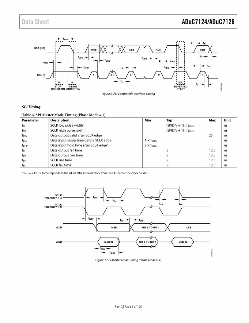
TIMING SPECIFICATIONS I2C Timing
Table 2. I2C Timing in Fast Mode (400 kHz) Slave Master Parameter Description Min Max Typ Unit tL SCL low pulse width 200 1360 ns tH SCL high pulse width 100 1140 ns tSHD Start condition hold time 300 ns tDSU Data setup time 100 740 ns tDHD Data hold time 0 400 ns tRSU Setup time for repeated start 100 ns tPSU Stop condition setup time 100 800 ns tBUF Bus-free time between a stop condition and a start condition 1.3 μs tR Rise time for both SCL and SDA 300 200 ns tF Fall time for both SCL and SDA 300 ns
Table 3. I2C Timing in Standard Mode (100 kHz) Slave Parameter Description Min Max Unit tL SCL low pulse width 4.7 μs tH SCL high pulse width 4.0 ns tSHD Start condition hold time 4.0 μs tDSU Data setup time 250 ns tDHD Data hold time 0 3.45 μs tRSU Setup time for repeated start 4.7 μs tPSU Stop condition setup time 4.0 μs tBUF Bus-free time between a stop condition and a start condition 4.7 μs tR Rise time for both SCL and SDA 1 μs tF Fall time for both SCL and SDA 300 ns
Data Sheet ADuC7124/ADuC7126
Rev. C | Page 9 of 108
SDA (I/O)
tBUF
MSB LSB ACK MSB
1982–71SCL (I)
P SSTOP
CONDITIONSTART
CONDITION
S(R)REPEATED
START
tR
tF
tF
tRtH
tL
tDSUtDHD
tRSU
tDHD
tDSU
tSHD
tPSU
0912
3-02
9
Figure 2. I2C-Compatible Interface Timing
SPI Timing
Table 4. SPI Master Mode Timing (Phase Mode = 1) Parameter Description Min Typ Max Unit tSL SCLK low pulse width1 (SPIDIV + 1) × tUCLK ns tSH SCLK high pulse width1
(SPIDIV + 1) × tUCLK ns tDAV Data output valid after SCLK edge 25 ns tDSU Data input setup time before SCLK edge1
1 × tUCLK ns tDHD Data input hold time after SCLK edge1
2 × tUCLK ns tDF Data output fall time 5 12.5 ns tDR Data output rise time 5 12.5 ns tSR SCLK rise time 5 12.5 ns tSF SCLK fall time 5 12.5 ns 1 tUCLK = 23.9 ns. It corresponds to the 41.78 MHz internal clock from the PLL before the clock divider.
0912
3-03
0
SCLK(POLARITY = 0)
SCLK(POLARITY = 1)
MOSI MSB BIT 6 TO BIT 1 LSB
MISO MSB IN BIT 6 TO BIT 1 LSB IN
tSHtSL
tSR tSF
tDRtDFtDAV
tDSUtDHD
Figure 3. SPI Master Mode Timing (Phase Mode = 1)

ADuC7124/ADuC7126 Data Sheet
Rev. C | Page 10 of 108
Table 5. SPI Master Mode Timing (Phase Mode = 0) Parameter Description Min Typ Max Unit tSL SCLK low pulse width1 (SPIDIV + 1) × tUCLK ns tSH SCLK high pulse width1
(SPIDIV + 1) × tUCLK ns tDAV Data output valid after SCLK edge 25 ns tDOSU Data output setup before SCLK edge 75 ns tDSU Data input setup time before SCLK edge1
1 × tUCLK ns tDHD Data input hold time after SCLK edge1
2 × tUCLK ns tDF Data output fall time 5 12.5 ns tDR Data output rise time 5 12.5 ns tSR SCLK rise time 5 12.5 ns tSF SCLK fall time 5 12.5 ns 1 tUCLK = 23.9 ns. It corresponds to the 41.78 MHz internal clock from the PLL before the clock divider.
0912
3-03
1
SCLK(POLARITY = 0)
SCLK(POLARITY = 1)
tSHtSL
tSR tSF
MOSI MSB BIT 6 TO BIT 1 LSB
MISO MSB IN BIT 6 TO BIT 1 LSB IN
tDRtDF
tDAVtDOSU
tDSU
tDHD
Figure 4. SPI Master Mode Timing (Phase Mode = 0)
Data Sheet ADuC7124/ADuC7126
Rev. C | Page 11 of 108
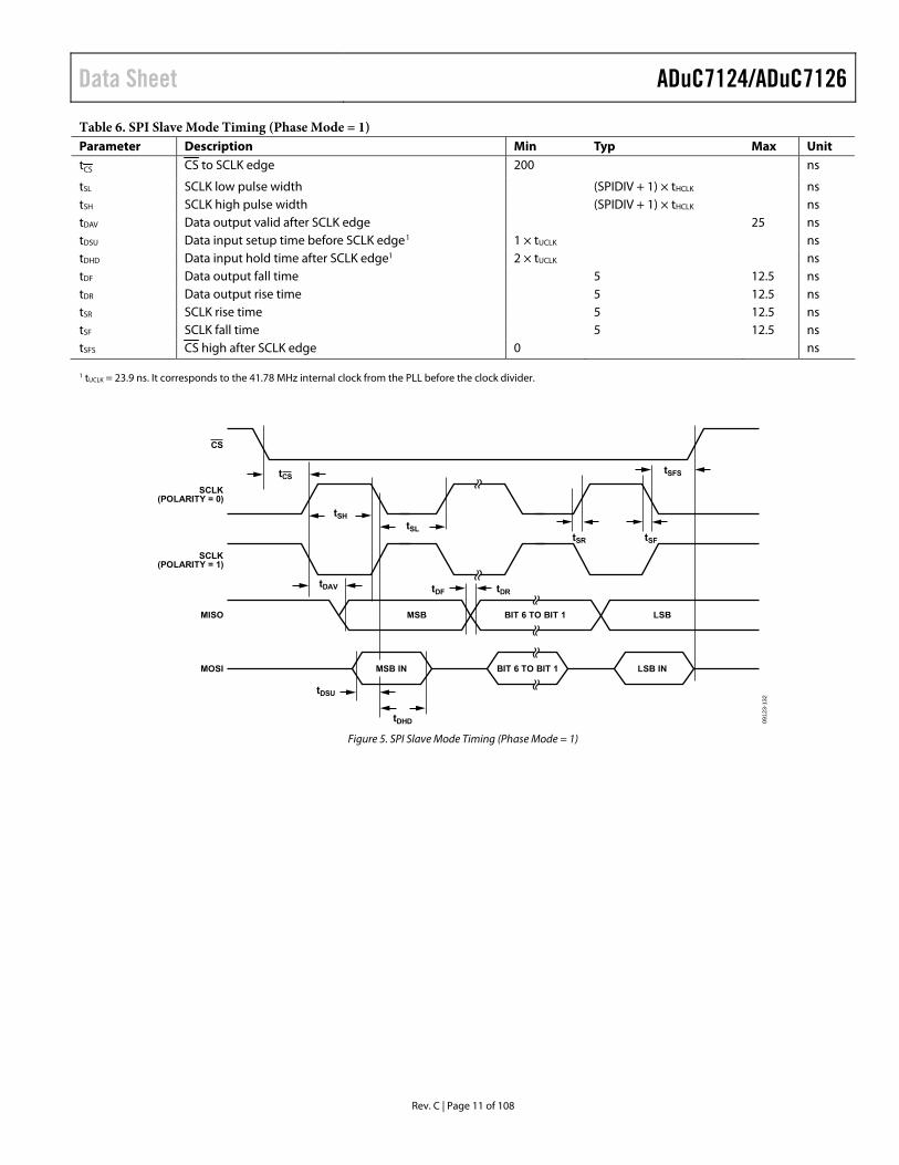
Table 6. SPI Slave Mode Timing (Phase Mode = 1) Parameter Description Min Typ Max Unit tCS CS to SCLK edge 200 ns
tSL SCLK low pulse width (SPIDIV + 1) × tHCLK ns tSH SCLK high pulse width (SPIDIV + 1) × tHCLK ns tDAV Data output valid after SCLK edge 25 ns tDSU Data input setup time before SCLK edge1 1 × tUCLK ns tDHD Data input hold time after SCLK edge1
2 × tUCLK ns tDF Data output fall time 5 12.5 ns tDR Data output rise time 5 12.5 ns tSR SCLK rise time 5 12.5 ns tSF SCLK fall time 5 12.5 ns tSFS CS high after SCLK edge 0 ns 1 tUCLK = 23.9 ns. It corresponds to the 41.78 MHz internal clock from the PLL before the clock divider.
0912
3-13
2
SCLK(POLARITY = 0)
CS
SCLK(POLARITY = 1)
tSHtSL
tSR tSF
tSFS
MISO MSB BIT 6 TO BIT 1 LSB
MOSI MSB IN BIT 6 TO BIT 1 LSB IN
tDHD
tDSU
tDAV tDRtDF
tCS
Figure 5. SPI Slave Mode Timing (Phase Mode = 1)

ADuC7124/ADuC7126 Data Sheet
Rev. C | Page 12 of 108
Table 7. SPI Slave Mode Timing (Phase Mode = 0) Parameter Description Min Typ Max Unit tCS CS to SCLK edge 200 ns
tSL SCLK low pulse width (SPIDIV + 1) × tHCLK ns tSH SCLK high pulse width (SPIDIV + 1) × tHCLK ns tDAV Data output valid after SCLK edge 25 ns tDSU Data input setup time before SCLK edge1 1 × tUCLK ns tDHD Data input hold time after SCLK edge1
2 × tUCLK ns tDF Data output fall time 5 12.5 ns tDR Data output rise time 5 12.5 ns tSR SCLK rise time 5 12.5 ns tSF SCLK fall time 5 12.5 ns tDOCS Data output valid after CS edge 25 ns
tSFS CS high after SCLK edge 0 ns 1 tUCLK = 23.9 ns. It corresponds to the 41.78 MHz internal clock from the PLL before the clock divider.
0912
3-03
3
SCLK(POLARITY = 0)
CS
SCLK(POLARITY = 1)
tSH tSLtSR tSF
tSFS
MISO
MOSI MSB IN BIT 6 TO BIT 1 LSB IN
tDHD
tDSU
MSB BIT 6 TO BIT 1 LSB
tDOCS
tDAV
tDRtDF
tCS
Figure 6. SPI Slave Mode Timing (Phase Mode = 0)
Data Sheet ADuC7124/ADuC7126
Rev. C | Page 13 of 108
ABSOLUTE MAXIMUM RATINGS AGND = GNDREF = DACGND = GNDREF, TA = 25°C, unless otherwise noted.
Table 8.
Stresses above those listed under Absolute Maximum Ratings may cause permanent damage to the device. This is a stress rating only; functional operation of the device at these or any other conditions above those indicated in the operational section of this specification is not implied. Exposure to absolute maximum rating conditions for extended periods may affect device reliability.
Only one absolute maximum rating can be applied at any one time.
ESD CAUTION
Parameter Rating AVDD to IOVDD −0.3 V to +0.3 V AGND to DGND −0.3 V to +0.3 V IOVDD to IOGND, AVDD to AGND −0.3 V to +6 V Digital Input Voltage to IOGND −0.3 V to +5.3 V Digital Output Voltage to IOGND −0.3 V to IOVDD + 0.3 V VREF to AGND −0.3 V to AVDD + 0.3 V Analog Inputs to AGND −0.3 V to AVDD + 0.3 V Analog Outputs to AGND −0.3 V to AVDD + 0.3 V Operating Temperature Range, Industrial –40°C to +125°C Storage Temperature Range −65°C to +150°C Junction Temperature 150°C θJA Thermal Impedance
64-Lead LFCSP 24°C/W 80-Lead LQFP 38°C/W
Peak Solder Reflow Temperature SnPb Assemblies (10 sec to 30 sec) 240°C RoHS Compliant Assemblies
(20 sec to 40 sec) 260°C
ADuC7124/ADuC7126 Data Sheet
Rev. C | Page 14 of 108
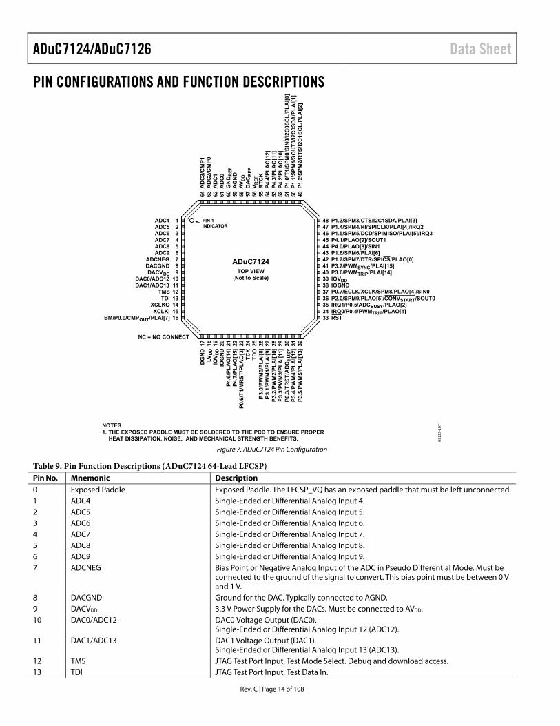
PIN CONFIGURATIONS AND FUNCTION DESCRIPTIONS
PIN 1INDICATOR
17 18 19 20 21 22 23 24 25 26 27 28 29 30 31 32
DG
ND
LVD
DIO
V DD
IOG
ND
P4.6
/PLA
O[1
4]P4
.7/P
LAO
[15]
P0.6
/T1/
MR
ST/P
LAO
[3]
TCK
TDO
P3.0
/PW
M0/
PLA
I[8]
P3.1
/PW
M1/
PLA
I[9]
P3.2
/PW
M2/
PLA
I[10]
P3.3
/PW
M3/
PLA
I[11]
P0.3
/TR
ST/A
DC
BUS
YP3
.4/P
WM
4/PL
AI[1
2]P3
.5/P
WM
5/PL
AI[1
3]
64 63 62 61 60 59 58 57 56 55 54 53 52 51 50 49
AD
C3/
CM
P1A
DC
2/C
MP0
AD
C1
AD
C0
GN
DR
EFA
GN
DAV
DD
DA
CRE
FV R
EFR
TCK
P4.4
/PLA
O[1
2]P4
.3/P
LAO
[11]
P4.2
/PLA
O[1
0]P1
.0/T
1/SP
M0/
SIN
0/I2
C0S
CL/
PLA
I[0]
P1.1
/SPM
1/SO
UT0
/I2C
0SD
A/P
LAI[1
]P1
.2/S
PM2/
RTS
/I2C
1SC
L/PL
AI[2
]
123456789
10111213141516
ADC4ADC5ADC6ADC7ADC8ADC9
ADCNEGDACGNDDACVDD
DAC0/ADC12DAC1/ADC13
TMSTDI
XCLKOXCLKI
BM/P0.0/CMPOUT/PLAI[7]
NC = NO CONNECT
P1.3/SPM3/CTS/I2C1SDA/PLAI[3]P1.4/SPM4/RI/SPICLK/PLAI[4]/IRQ2P1.5/SPM5/DCD/SPIMISO/PLAI[5]/IRQ3P4.1/PLAO[9]/SOUT1P4.0/PLAO[8]/SIN1P1.6/SPM6/PLAI[6]P1.7/SPM7/DTR/SPICS/PLAO[0]P3.7/PWMSYNC/PLAI[15]P3.6/PWMTRIP/PLAI[14]IOVDDIOGNDP0.7/ECLK/XCLK/SPM8/PLAO[4]/SIN0P2.0/SPM9/PLAO[5]/CONVSTART/SOUT0IRQ1/P0.5/ADCBUSY/PLAO[2]IRQ0/P0.4/PWMTRIP/PLAO[1]RST
48474645444342414039383736353433
ADuC7124TOP VIEW
(Not to Scale)
0912
3-10
7NOTES1. THE EXPOSED PADDLE MUST BE SOLDERED TO THE PCB TO ENSURE PROPER HEAT DISSIPATION, NOISE, AND MECHANICAL STRENGTH BENEFITS.
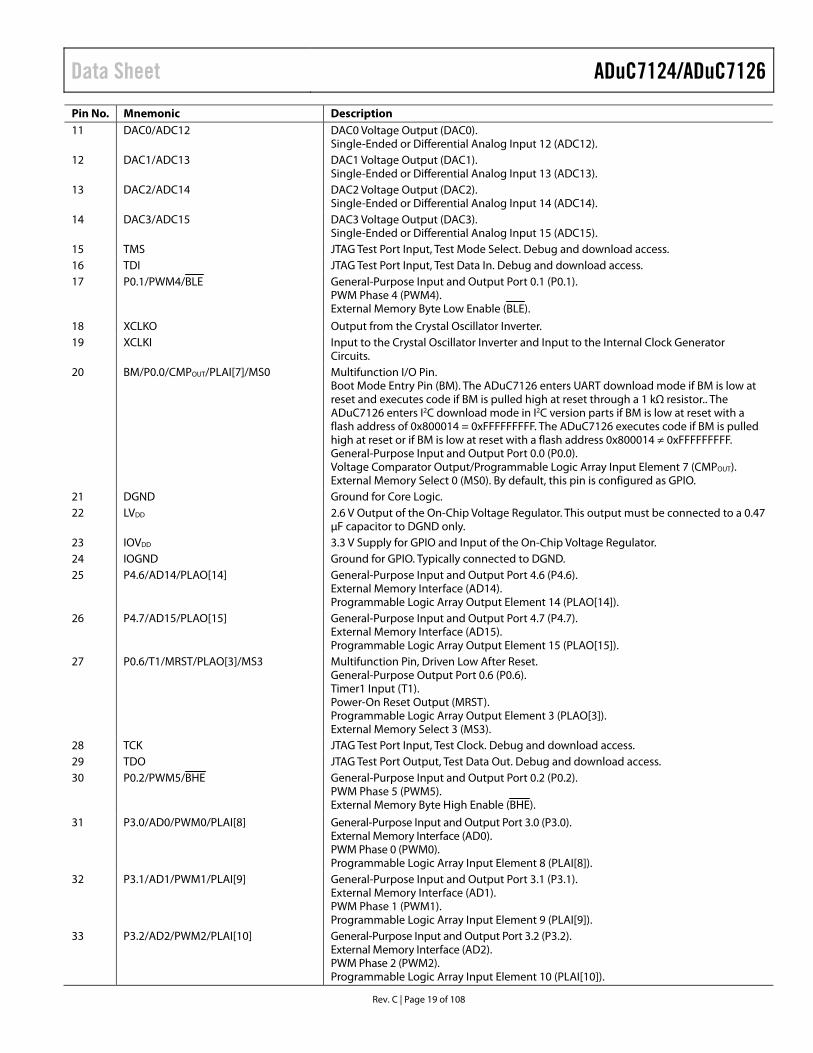
Figure 7. ADuC7124 Pin Configuration
Table 9. Pin Function Descriptions (ADuC7124 64-Lead LFCSP) Pin No. Mnemonic Description 0 Exposed Paddle Exposed Paddle. The LFCSP_VQ has an exposed paddle that must be left unconnected. 1 ADC4 Single-Ended or Differential Analog Input 4. 2 ADC5 Single-Ended or Differential Analog Input 5. 3 ADC6 Single-Ended or Differential Analog Input 6. 4 ADC7 Single-Ended or Differential Analog Input 7. 5 ADC8 Single-Ended or Differential Analog Input 8. 6 ADC9 Single-Ended or Differential Analog Input 9. 7 ADCNEG Bias Point or Negative Analog Input of the ADC in Pseudo Differential Mode. Must be
connected to the ground of the signal to convert. This bias point must be between 0 V and 1 V.
8 DACGND Ground for the DAC. Typically connected to AGND. 9 DACVDD 3.3 V Power Supply for the DACs. Must be connected to AVDD. 10 DAC0/ADC12 DAC0 Voltage Output (DAC0).
Single-Ended or Differential Analog Input 12 (ADC12). 11 DAC1/ADC13 DAC1 Voltage Output (DAC1).
Single-Ended or Differential Analog Input 13 (ADC13). 12 TMS JTAG Test Port Input, Test Mode Select. Debug and download access. 13 TDI JTAG Test Port Input, Test Data In.
Data Sheet ADuC7124/ADuC7126
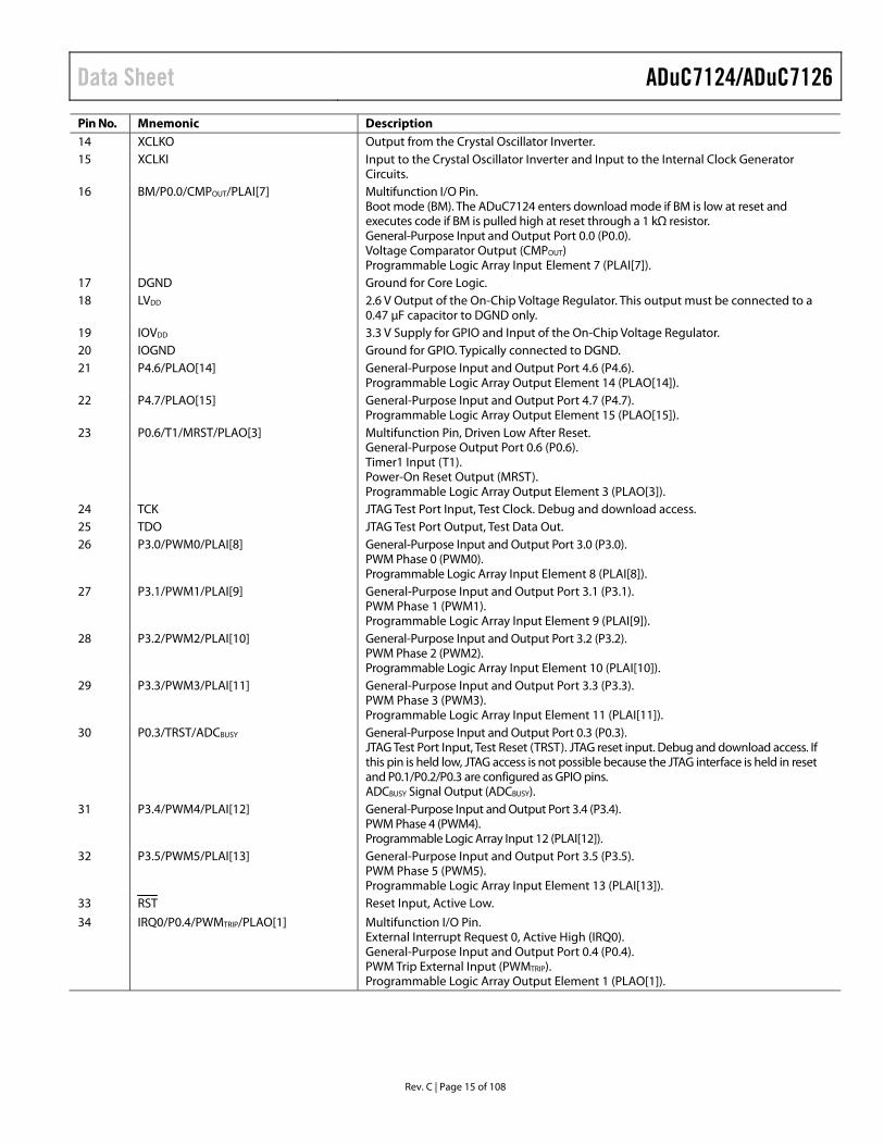
Rev. C | Page 15 of 108
Pin No. Mnemonic Description 14 XCLKO Output from the Crystal Oscillator Inverter. 15 XCLKI Input to the Crystal Oscillator Inverter and Input to the Internal Clock Generator
Circuits. 16 BM/P0.0/CMPOUT/PLAI[7] Multifunction I/O Pin.
Boot mode (BM). The ADuC7124 enters download mode if BM is low at reset and executes code if BM is pulled high at reset through a 1 kΩ resistor. General-Purpose Input and Output Port 0.0 (P0.0). Voltage Comparator Output (CMPOUT) Programmable Logic Array Input Element 7 (PLAI[7]).
17 DGND Ground for Core Logic. 18 LVDD 2.6 V Output of the On-Chip Voltage Regulator. This output must be connected to a
0.47 μF capacitor to DGND only. 19 IOVDD 3.3 V Supply for GPIO and Input of the On-Chip Voltage Regulator. 20 IOGND Ground for GPIO. Typically connected to DGND. 21 P4.6/PLAO[14] General-Purpose Input and Output Port 4.6 (P4.6).
Programmable Logic Array Output Element 14 (PLAO[14]). 22 P4.7/PLAO[15] General-Purpose Input and Output Port 4.7 (P4.7).
Programmable Logic Array Output Element 15 (PLAO[15]). 23 P0.6/T1/MRST/PLAO[3] Multifunction Pin, Driven Low After Reset.
General-Purpose Output Port 0.6 (P0.6). Timer1 Input (T1). Power-On Reset Output (MRST). Programmable Logic Array Output Element 3 (PLAO[3]).
24 TCK JTAG Test Port Input, Test Clock. Debug and download access. 25 TDO JTAG Test Port Output, Test Data Out. 26 P3.0/PWM0/PLAI[8] General-Purpose Input and Output Port 3.0 (P3.0).
PWM Phase 0 (PWM0). Programmable Logic Array Input Element 8 (PLAI[8]).
27 P3.1/PWM1/PLAI[9] General-Purpose Input and Output Port 3.1 (P3.1). PWM Phase 1 (PWM1). Programmable Logic Array Input Element 9 (PLAI[9]).
28 P3.2/PWM2/PLAI[10] General-Purpose Input and Output Port 3.2 (P3.2). PWM Phase 2 (PWM2). Programmable Logic Array Input Element 10 (PLAI[10]).
29 P3.3/PWM3/PLAI[11] General-Purpose Input and Output Port 3.3 (P3.3). PWM Phase 3 (PWM3). Programmable Logic Array Input Element 11 (PLAI[11]).
30 P0.3/TRST/ADCBUSY General-Purpose Input and Output Port 0.3 (P0.3). JTAG Test Port Input, Test Reset (TRST). JTAG reset input. Debug and download access. If this pin is held low, JTAG access is not possible because the JTAG interface is held in reset and P0.1/P0.2/P0.3 are configured as GPIO pins. ADCBUSY Signal Output (ADCBUSY).
31 P3.4/PWM4/PLAI[12] General-Purpose Input and Output Port 3.4 (P3.4). PWM Phase 4 (PWM4). Programmable Logic Array Input 12 (PLAI[12]).
32 P3.5/PWM5/PLAI[13] General-Purpose Input and Output Port 3.5 (P3.5). PWM Phase 5 (PWM5). Programmable Logic Array Input Element 13 (PLAI[13]).
33 RST Reset Input, Active Low.
34 IRQ0/P0.4/PWMTRIP/PLAO[1] Multifunction I/O Pin. External Interrupt Request 0, Active High (IRQ0). General-Purpose Input and Output Port 0.4 (P0.4). PWM Trip External Input (PWMTRIP). Programmable Logic Array Output Element 1 (PLAO[1]).
ADuC7124/ADuC7126 Data Sheet
Rev. C | Page 16 of 108
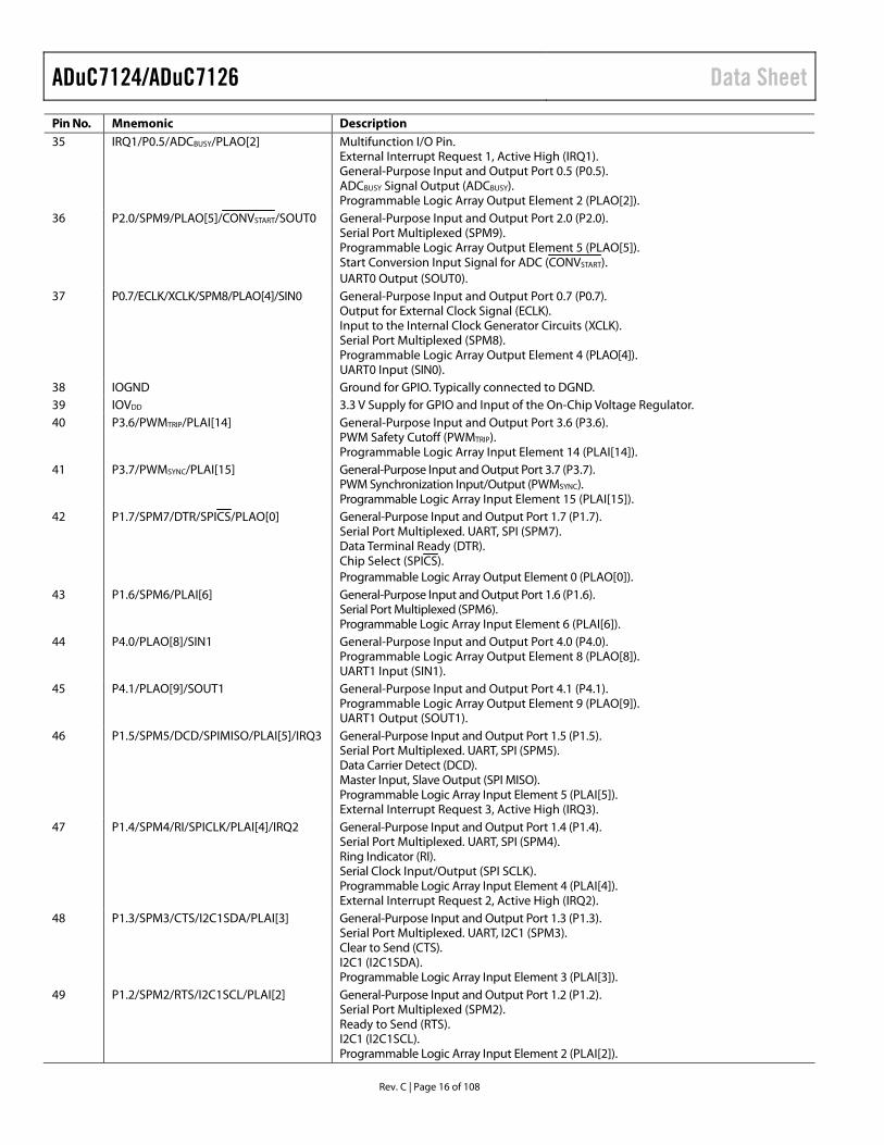
Pin No. Mnemonic Description 35 IRQ1/P0.5/ADCBUSY/PLAO[2] Multifunction I/O Pin.
External Interrupt Request 1, Active High (IRQ1). General-Purpose Input and Output Port 0.5 (P0.5). ADCBUSY Signal Output (ADCBUSY). Programmable Logic Array Output Element 2 (PLAO[2]).
36 P2.0/SPM9/PLAO[5]/CONVSTART/SOUT0 General-Purpose Input and Output Port 2.0 (P2.0). Serial Port Multiplexed (SPM9). Programmable Logic Array Output Element 5 (PLAO[5]). Start Conversion Input Signal for ADC (CONVSTART). UART0 Output (SOUT0).
37 P0.7/ECLK/XCLK/SPM8/PLAO[4]/SIN0 General-Purpose Input and Output Port 0.7 (P0.7). Output for External Clock Signal (ECLK). Input to the Internal Clock Generator Circuits (XCLK). Serial Port Multiplexed (SPM8). Programmable Logic Array Output Element 4 (PLAO[4]). UART0 Input (SIN0).
38 IOGND Ground for GPIO. Typically connected to DGND. 39 IOVDD 3.3 V Supply for GPIO and Input of the On-Chip Voltage Regulator. 40 P3.6/PWMTRIP/PLAI[14] General-Purpose Input and Output Port 3.6 (P3.6).
PWM Safety Cutoff (PWMTRIP). Programmable Logic Array Input Element 14 (PLAI[14]).
41 P3.7/PWMSYNC/PLAI[15] General-Purpose Input and Output Port 3.7 (P3.7). PWM Synchronization Input/Output (PWMSYNC). Programmable Logic Array Input Element 15 (PLAI[15]).
42 P1.7/SPM7/DTR/SPICS/PLAO[0] General-Purpose Input and Output Port 1.7 (P1.7). Serial Port Multiplexed. UART, SPI (SPM7). Data Terminal Ready (DTR). Chip Select (SPICS). Programmable Logic Array Output Element 0 (PLAO[0]).
43 P1.6/SPM6/PLAI[6] General-Purpose Input and Output Port 1.6 (P1.6). Serial Port Multiplexed (SPM6). Programmable Logic Array Input Element 6 (PLAI[6]).
44 P4.0/PLAO[8]/SIN1 General-Purpose Input and Output Port 4.0 (P4.0). Programmable Logic Array Output Element 8 (PLAO[8]). UART1 Input (SIN1).
45 P4.1/PLAO[9]/SOUT1 General-Purpose Input and Output Port 4.1 (P4.1). Programmable Logic Array Output Element 9 (PLAO[9]). UART1 Output (SOUT1).
46 P1.5/SPM5/DCD/SPIMISO/PLAI[5]/IRQ3 General-Purpose Input and Output Port 1.5 (P1.5). Serial Port Multiplexed. UART, SPI (SPM5). Data Carrier Detect (DCD). Master Input, Slave Output (SPI MISO). Programmable Logic Array Input Element 5 (PLAI[5]). External Interrupt Request 3, Active High (IRQ3).
47 P1.4/SPM4/RI/SPICLK/PLAI[4]/IRQ2 General-Purpose Input and Output Port 1.4 (P1.4). Serial Port Multiplexed. UART, SPI (SPM4). Ring Indicator (RI). Serial Clock Input/Output (SPI SCLK). Programmable Logic Array Input Element 4 (PLAI[4]). External Interrupt Request 2, Active High (IRQ2).
48 P1.3/SPM3/CTS/I2C1SDA/PLAI[3] General-Purpose Input and Output Port 1.3 (P1.3). Serial Port Multiplexed. UART, I2C1 (SPM3). Clear to Send (CTS). I2C1 (I2C1SDA). Programmable Logic Array Input Element 3 (PLAI[3]).
49 P1.2/SPM2/RTS/I2C1SCL/PLAI[2] General-Purpose Input and Output Port 1.2 (P1.2). Serial Port Multiplexed (SPM2). Ready to Send (RTS). I2C1 (I2C1SCL). Programmable Logic Array Input Element 2 (PLAI[2]).
Data Sheet ADuC7124/ADuC7126
Rev. C | Page 17 of 108
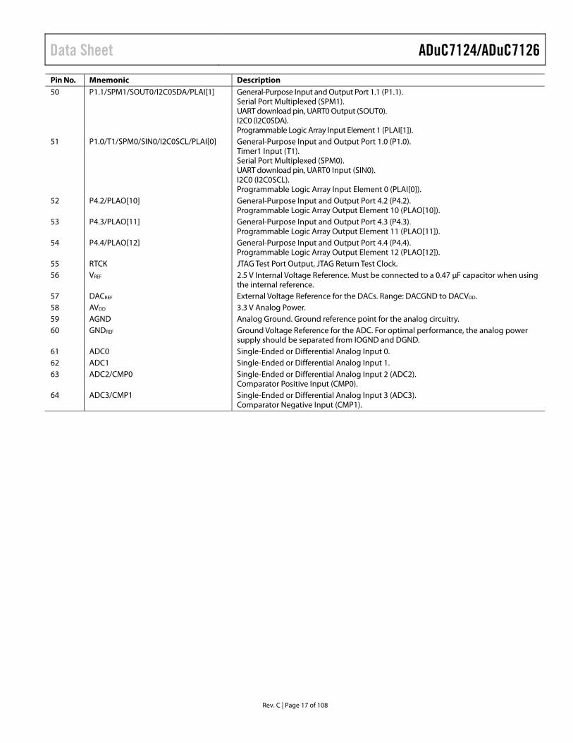
Pin No. Mnemonic Description 50 P1.1/SPM1/SOUT0/I2C0SDA/PLAI[1] General-Purpose Input and Output Port 1.1 (P1.1).
Serial Port Multiplexed (SPM1). UART download pin, UART0 Output (SOUT0). I2C0 (I2C0SDA). Programmable Logic Array Input Element 1 (PLAI[1]).
51 P1.0/T1/SPM0/SIN0/I2C0SCL/PLAI[0] General-Purpose Input and Output Port 1.0 (P1.0). Timer1 Input (T1). Serial Port Multiplexed (SPM0). UART download pin, UART0 Input (SIN0). I2C0 (I2C0SCL). Programmable Logic Array Input Element 0 (PLAI[0]).
52 P4.2/PLAO[10] General-Purpose Input and Output Port 4.2 (P4.2). Programmable Logic Array Output Element 10 (PLAO[10]).
53 P4.3/PLAO[11] General-Purpose Input and Output Port 4.3 (P4.3). Programmable Logic Array Output Element 11 (PLAO[11]).
54 P4.4/PLAO[12] General-Purpose Input and Output Port 4.4 (P4.4). Programmable Logic Array Output Element 12 (PLAO[12]).
55 RTCK JTAG Test Port Output, JTAG Return Test Clock. 56 VREF 2.5 V Internal Voltage Reference. Must be connected to a 0.47 μF capacitor when using
the internal reference. 57 DACREF External Voltage Reference for the DACs. Range: DACGND to DACVDD. 58 AVDD 3.3 V Analog Power. 59 AGND Analog Ground. Ground reference point for the analog circuitry. 60 GNDREF Ground Voltage Reference for the ADC. For optimal performance, the analog power
supply should be separated from IOGND and DGND. 61 ADC0 Single-Ended or Differential Analog Input 0. 62 ADC1 Single-Ended or Differential Analog Input 1. 63 ADC2/CMP0 Single-Ended or Differential Analog Input 2 (ADC2).
Comparator Positive Input (CMP0). 64 ADC3/CMP1 Single-Ended or Differential Analog Input 3 (ADC3).
Comparator Negative Input (CMP1).
ADuC7124/ADuC7126 Data Sheet
Rev. C | Page 18 of 108
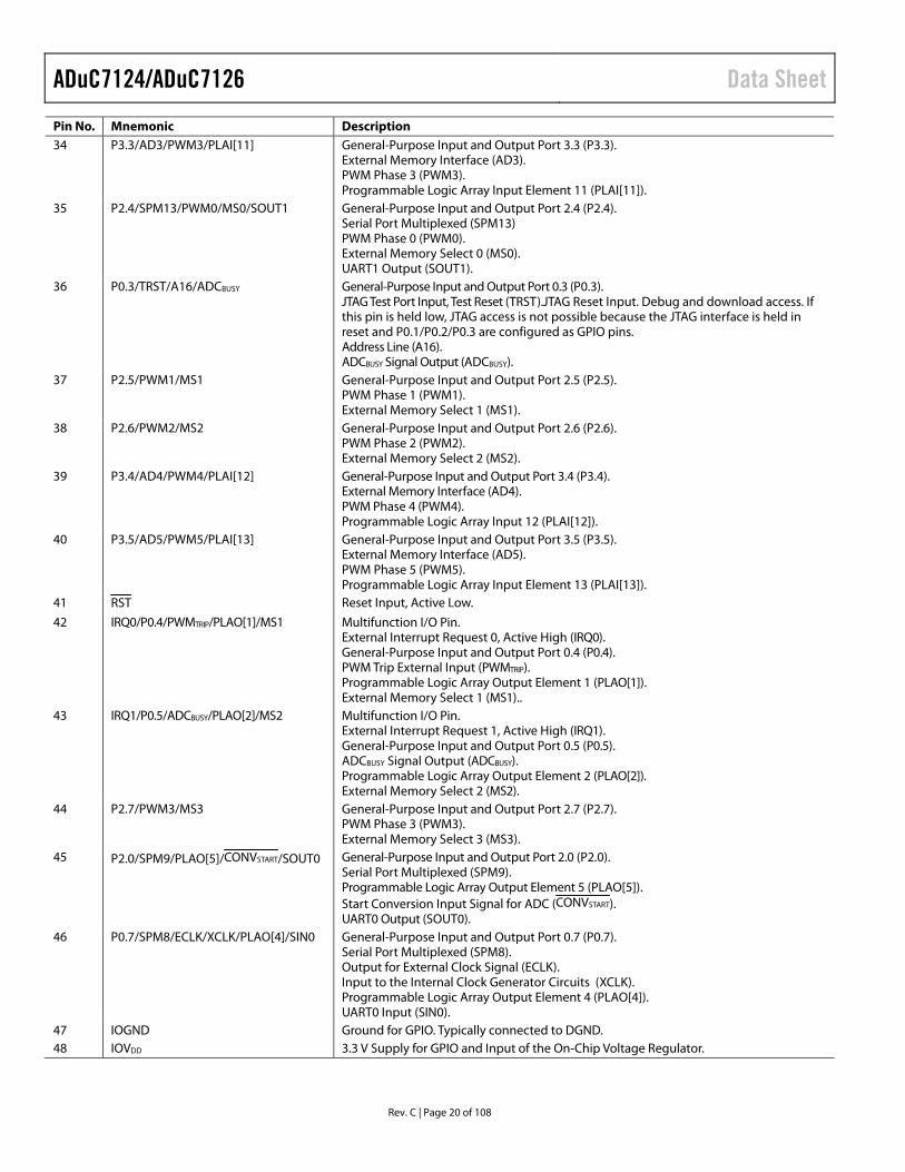
2ADC53ADC64ADC7
7ADC10
6ADC9
5ADC8
1ADC4
8ADCNEG9DACGND
10DACVDD
12DAC1/ADC1313DAC2/ADC1414DAC3/ADC1515TMS16TDI17P0.1/PWM4/BLE18XCLKO19XCLKI20BM/P0.0/CMPOUT/PLAI[7]/MS0
11DAC0/ADC12
59
58
57
54
55
56
60
53
52
P1.4/SPM4/RI/SPICLK/PLAI[4]/IRQ2P1.5/SPM5/DCD/SPIMISO/PLAI[5]/IRQ3P4.1/SPM11/SOUT1/AD9/PLAO[9]
P1.7/SPM7/DTR/SPICS/PLAO[0]P1.6/SPM6/PLAI[6]P4.0/SPM10/SIN1/AD8/PLAO[8]
P1.3/SPM3/CTS/I2C1SDA/PLAI[3]
P3.7/AD7/PWMSYNC/PLAI[15]P3.6/AD6/PWMTRIP/PLAI[14]
51 P2.2/RS/PWM1/PLAO[7]
49 P2.3/SPM12/AE/SIN148 IOVDD47 IOGND46 P0.7/SPM8/ECLK/XCLK/PLAO[4]/SIN045 P2.0/SPM9/PLAO[5]/CONVSTART/SOUT044 P2.7/PWM3/MS343 IRQ1/P0.5/ADCBUSY/PLAO[2]/MS242 IRQ0/P0.4/PWMTRIP/PLAO[1]/MS141 RST
50 P2.1/WS/PWM0/PLAO[6]
21
DG
ND
22
LVDD
23
IOV D
D
24
IOG
ND
25
P4.6
/AD
14/P
LAO
[14]
26
P4.7
/AD
15/P
LAO
[15]
27
P0.6
/T1/
MR
ST/P
LAO
[3]/M
S3
28
TCK
29
TDO
30
P0.2
/PW
M5/
BH
E
31
P3.0
/AD
0/PW
M0/
PLA
I[8]
32
P3.1
/AD
1/PW
M1/
PLA
I[9]
33
P3.2
/AD
2/PW
M2/
PLA
I[10]
34
P3.3
/AD
3/PW
M3/
PLA
I[11]
35
P2.4
/SPM
13/P
WM
0/M
S0/S
OU
T1
36
P0.3
/TR
ST/A
16/A
DC
BUS
Y
37
P2.5
/PW
M1/
MS1
38
P2.6
/PW
M2/
MS2
39
P3.4
/AD
4/PW
M4/
PLA
I[12]
40
P3.5
/AD
5/PW
M5/
PLA
I[13]
80A
DC
3/C
MP1
79A
DC
2/C
MP0
78
AD
C1
77
AD
C0
76
AD
C11
75
GN
DR
EF
74
AG
ND
73
AG
ND
72
AVD
D
71
DA
CRE
F
70
V REF
69
IOG
ND
68
IOV D
D
67
P4.5
/AD
13/P
LAO
[13]
/RTC
K
66
P4.4
/AD
12/P
LAO
[12]
65
P4.3
/AD
11/P
LAO
[11]
64
P4.2
/AD
10/P
LAO
[10]
63
P1.0
/T1/
SPM
0/SI
N0/
I2C
0SC
L/PL
AI[0
]
62
P1.1
/SPM
1/SO
UT0
/I2C
0SD
A/P
LAI[1
]
61
P1.2
/SPM
2/R
TS/I2
C1S
CL/
PLA
I[2]
PIN 1
TOP VIEW
0912
3-10
8
ADuC7126
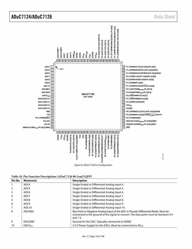
Figure 8. ADuC7126 Pin Configuration
Table 10. Pin Function Descriptions (ADuC7126 80-Lead LQFP) Pin No. Mnemonic Description 1 ADC4 Single-Ended or Differential Analog Input 4. 2 ADC5 Single-Ended or Differential Analog Input 5. 3 ADC6 Single-Ended or Differential Analog Input 6. 4 ADC7 Single-Ended or Differential Analog Input 7. 5 ADC8 Single-Ended or Differential Analog Input 8. 6 ADC9 Single-Ended or Differential Analog Input 9. 7 ADC10 Single-Ended or Differential Analog Input 10. 8 ADCNEG Bias Point or Negative Analog Input of the ADC in Pseudo Differential Mode. Must be
connected to the ground of the signal to convert. This bias point must be between 0 V and 1 V.
9 DACGND Ground for the DAC. Typically connected to AGND. 10 DACVDD 3.3 V Power Supply for the DACs. Must be connected to AVDD.
Data Sheet ADuC7124/ADuC7126
Rev. C | Page 19 of 108
Pin No. Mnemonic Description 11 DAC0/ADC12 DAC0 Voltage Output (DAC0).
Single-Ended or Differential Analog Input 12 (ADC12). 12 DAC1/ADC13 DAC1 Voltage Output (DAC1).
Single-Ended or Differential Analog Input 13 (ADC13). 13 DAC2/ADC14 DAC2 Voltage Output (DAC2).
Single-Ended or Differential Analog Input 14 (ADC14). 14 DAC3/ADC15 DAC3 Voltage Output (DAC3).
Single-Ended or Differential Analog Input 15 (ADC15). 15 TMS JTAG Test Port Input, Test Mode Select. Debug and download access. 16 TDI JTAG Test Port Input, Test Data In. Debug and download access. 17 P0.1/PWM4/BLE General-Purpose Input and Output Port 0.1 (P0.1).
PWM Phase 4 (PWM4). External Memory Byte Low Enable (BLE).
18 XCLKO Output from the Crystal Oscillator Inverter. 19 XCLKI Input to the Crystal Oscillator Inverter and Input to the Internal Clock Generator
Circuits. 20 BM/P0.0/CMPOUT/PLAI[7]/MS0 Multifunction I/O Pin.
Boot Mode Entry Pin (BM). The ADuC7126 enters UART download mode if BM is low at reset and executes code if BM is pulled high at reset through a 1 kΩ resistor.. The ADuC7126 enters I2C download mode in I2C version parts if BM is low at reset with a flash address of 0x800014 = 0xFFFFFFFFF. The ADuC7126 executes code if BM is pulled high at reset or if BM is low at reset with a flash address 0x800014 ≠ 0xFFFFFFFFF. General-Purpose Input and Output Port 0.0 (P0.0). Voltage Comparator Output/Programmable Logic Array Input Element 7 (CMPOUT). External Memory Select 0 (MS0). By default, this pin is configured as GPIO.
21 DGND Ground for Core Logic. 22 LVDD 2.6 V Output of the On-Chip Voltage Regulator. This output must be connected to a 0.47
μF capacitor to DGND only. 23 IOVDD 3.3 V Supply for GPIO and Input of the On-Chip Voltage Regulator. 24 IOGND Ground for GPIO. Typically connected to DGND. 25 P4.6/AD14/PLAO[14] General-Purpose Input and Output Port 4.6 (P4.6).
External Memory Interface (AD14). Programmable Logic Array Output Element 14 (PLAO[14]).
26 P4.7/AD15/PLAO[15] General-Purpose Input and Output Port 4.7 (P4.7). External Memory Interface (AD15). Programmable Logic Array Output Element 15 (PLAO[15]).
27 P0.6/T1/MRST/PLAO[3]/MS3 Multifunction Pin, Driven Low After Reset. General-Purpose Output Port 0.6 (P0.6). Timer1 Input (T1). Power-On Reset Output (MRST). Programmable Logic Array Output Element 3 (PLAO[3]). External Memory Select 3 (MS3).
28 TCK JTAG Test Port Input, Test Clock. Debug and download access. 29 TDO JTAG Test Port Output, Test Data Out. Debug and download access. 30 P0.2/PWM5/BHE General-Purpose Input and Output Port 0.2 (P0.2).
PWM Phase 5 (PWM5). External Memory Byte High Enable (BHE).
31 P3.0/AD0/PWM0/PLAI[8] General-Purpose Input and Output Port 3.0 (P3.0). External Memory Interface (AD0). PWM Phase 0 (PWM0). Programmable Logic Array Input Element 8 (PLAI[8]).
32 P3.1/AD1/PWM1/PLAI[9] General-Purpose Input and Output Port 3.1 (P3.1). External Memory Interface (AD1). PWM Phase 1 (PWM1). Programmable Logic Array Input Element 9 (PLAI[9]).
33 P3.2/AD2/PWM2/PLAI[10] General-Purpose Input and Output Port 3.2 (P3.2). External Memory Interface (AD2). PWM Phase 2 (PWM2). Programmable Logic Array Input Element 10 (PLAI[10]).
ADuC7124/ADuC7126 Data Sheet
Rev. C | Page 20 of 108
Pin No. Mnemonic Description 34 P3.3/AD3/PWM3/PLAI[11] General-Purpose Input and Output Port 3.3 (P3.3).
External Memory Interface (AD3). PWM Phase 3 (PWM3). Programmable Logic Array Input Element 11 (PLAI[11]).
35 P2.4/SPM13/PWM0/MS0/SOUT1 General-Purpose Input and Output Port 2.4 (P2.4). Serial Port Multiplexed (SPM13) PWM Phase 0 (PWM0). External Memory Select 0 (MS0). UART1 Output (SOUT1).
36 P0.3/TRST/A16/ADCBUSY General-Purpose Input and Output Port 0.3 (P0.3). JTAG Test Port Input, Test Reset (TRST).JTAG Reset Input. Debug and download access. If this pin is held low, JTAG access is not possible because the JTAG interface is held in reset and P0.1/P0.2/P0.3 are configured as GPIO pins. Address Line (A16). ADCBUSY Signal Output (ADCBUSY).
37 P2.5/PWM1/MS1 General-Purpose Input and Output Port 2.5 (P2.5). PWM Phase 1 (PWM1). External Memory Select 1 (MS1).
38 P2.6/PWM2/MS2 General-Purpose Input and Output Port 2.6 (P2.6). PWM Phase 2 (PWM2). External Memory Select 2 (MS2).
39 P3.4/AD4/PWM4/PLAI[12] General-Purpose Input and Output Port 3.4 (P3.4). External Memory Interface (AD4). PWM Phase 4 (PWM4). Programmable Logic Array Input 12 (PLAI[12]).
40 P3.5/AD5/PWM5/PLAI[13] General-Purpose Input and Output Port 3.5 (P3.5). External Memory Interface (AD5). PWM Phase 5 (PWM5). Programmable Logic Array Input Element 13 (PLAI[13]).
41 RST Reset Input, Active Low.
42 IRQ0/P0.4/PWMTRIP/PLAO[1]/MS1 Multifunction I/O Pin. External Interrupt Request 0, Active High (IRQ0). General-Purpose Input and Output Port 0.4 (P0.4). PWM Trip External Input (PWMTRIP). Programmable Logic Array Output Element 1 (PLAO[1]). External Memory Select 1 (MS1)..
43 IRQ1/P0.5/ADCBUSY/PLAO[2]/MS2 Multifunction I/O Pin. External Interrupt Request 1, Active High (IRQ1). General-Purpose Input and Output Port 0.5 (P0.5). ADCBUSY Signal Output (ADCBUSY). Programmable Logic Array Output Element 2 (PLAO[2]). External Memory Select 2 (MS2).
44 P2.7/PWM3/MS3 General-Purpose Input and Output Port 2.7 (P2.7). PWM Phase 3 (PWM3). External Memory Select 3 (MS3).
45 P2.0/SPM9/PLAO[5]/CONVSTART/SOUT0 General-Purpose Input and Output Port 2.0 (P2.0). Serial Port Multiplexed (SPM9). Programmable Logic Array Output Element 5 (PLAO[5]). Start Conversion Input Signal for ADC (CONVSTART). UART0 Output (SOUT0).
46 P0.7/SPM8/ECLK/XCLK/PLAO[4]/SIN0 General-Purpose Input and Output Port 0.7 (P0.7). Serial Port Multiplexed (SPM8). Output for External Clock Signal (ECLK). Input to the Internal Clock Generator Circuits (XCLK). Programmable Logic Array Output Element 4 (PLAO[4]). UART0 Input (SIN0).
47 IOGND Ground for GPIO. Typically connected to DGND. 48 IOVDD 3.3 V Supply for GPIO and Input of the On-Chip Voltage Regulator.
Data Sheet ADuC7124/ADuC7126
Rev. C | Page 21 of 108
Pin No. Mnemonic Description 49 P2.3/SPM12/AE/SIN1 General-Purpose Input and Output Port 2.3 (P2.3).
Serial Port Multiplexed (SPM12). External Memory Access Enable (AE). UART1 Input (SIN1).
50 P2.1/WS/PWM0/PLAO[6] General-Purpose Input and Output Port 2.1 (P2.1). External Memory Write Strobe (WS). PWM Phase 0 (PWM0). Programmable Logic Array Output Element 6 (PLAO[6]).
51 P2.2/RS/PWM1/PLAO[7] General-Purpose Input and Output Port 2.2 (P2.2). External Memory Read Strobe (RS). PWM Phase 1 (PWM1). Programmable Logic Array Output Element 7 (PLAO[7]).
52 P3.6/AD6/PWMTRIP/PLAI[14] General-Purpose Input and Output Port 3.6 (P3.6). External Memory Interface (AD6). PWM Safety Cutouff (PWMTRIP). Programmable Logic Array Input Element 14 (PLAI[14]).
53 P3.7/AD7/PWMSYNC/PLAI[15] General-Purpose Input and Output Port 3.7 (P3.7). External Memory Interface (AD7). PWM Synchronization (PWMSYNC). Programmable Logic Array Input Element 15 (PLAI[15]).
54 P1.7/SPM7/DTR/SPICS/PLAO[0] General-Purpose Input and Output Port 1.7 (P1.7). Serial Port Multiplexed (SPM7). Data Terminal Ready (DTR). Chip Select (SPICS). Programmable Logic Array Output Element 0 (PLAO[0]).
55 P1.6/SPM6/PLAI[6] General-Purpose Input and Output Port 1.6 (P1.6). Serial Port Multiplexed (SPM6). Programmable Logic Array Input Element 6 (PLAI[6]).
56 P4.0/SPM10/SIN1/AD8/PLAO[8] General-Purpose Input and Output Port 4.0 (P4.0). Serial Port Multiplexed (SPM10). UART1 Input (SIN1). External Memory Interface (AD8). Programmable Logic Array Output Element 8 (PLAO[8]).
57 P4.1/SPM11/SOUT1/AD9/PLAO[9] General-Purpose Input and Output Port 4.1 (P4.1). Serial Port Multiplexed (SPM11). UART1 Output (SOUT1). External Memory Interface (AD9). Programmable Logic Array Output Element 9 (PLAO[9]).
58 P1.5/SPM5/DCD/SPIMISO/PLAI[5]/IRQ3 General-Purpose Input and Output Port 1.5 (P1.5). Serial Port Multiplexed (SPM5). Data Carrier Detect (DCD). Master Input, Slave Output (SPI MISO). Programmable Logic Array Input Element 5 (PLAI[5]). External Interrupt Request 3, Active High (IRQ3).
59 P1.4/SPM4/RI/SPICLK/PLAI[4]/IRQ2 General-Purpose Input and Output Port 1.4 (P1.4). Serial Port Multiplexed (SPM4). Ring Indicator (RI). Serial Clock Input/Output (SPI SCLK). Programmable Logic Array Input Element 4 (PLAI[4]). External Interrupt Request 2, Active High (IRQ2).
60 P1.3/SPM3/CTS/I2C1SDA/PLAI[3] General-Purpose Input and Output Port 1.3 (P1.3). Serial Port Multiplexed (SPM3). Clear to Send (CTS). I2C1 (I2C1SDA). Programmable Logic Array Input Element 3 (PLAI[3]).
61 P1.2/SPM2/RTS/I2C1SCL/PLAI[2] General-Purpose Input and Output Port 1.2 (P1.2). Serial Port Multiplexed (SPM2). Ready to Send (RTS). I2C1 (I2C1SCL). Programmable Logic Array Input Element 2 (PLAI[2]).

ADuC7124/ADuC7126 Data Sheet
Rev. C | Page 22 of 108
Pin No. Mnemonic Description 62 P1.1/SPM1/SOUT0/I2C0SDA/PLAI[1] General-Purpose Input and Output Port 1.1 (P1.1).
Serial Port Multiplexed (SPM1). UART0 Output (SOUT0). I2C0 (I2C0SDA). Programmable Logic Array Input Element 1 (PLAI[1]).
63 P1.0/T1/SPM0/SIN0/I2C0SCL/PLAI[0] General-Purpose Input and Output Port 1.0 (P1.0). Timer1 Input (T1). Serial Port Multiplexed (SPM0). UART0 Input (SIN0). I2C0 (I2C0SCL). Programmable Logic Array Input Element 0 (PLAI[0]).
64 P4.2/AD10/PLAO[10] General-Purpose Input and Output Port 4.2 (P4.2). External Memory Interface (AD10). Programmable Logic Array Output Element 10 (PLAO[10]).
65 P4.3/AD11/PLAO[11] General-Purpose Input and Output Port 4.3 (P4.3). External Memory Interface (AD11). Programmable Logic Array Output Element 11 (PLAO[11]).
66 P4.4/AD12/PLAO[12] General-Purpose Input and Output Port 4.4 (P4.4). External Memory Interface (AD12). Programmable Logic Array Output Element 12 (PLAO[12]).
67 P4.5/AD13/PLAO[13]/RTCK General-Purpose Input and Output Port 4.5 (P4.5). External Memory Interface (AD13). Programmable Logic Array Output Element 13 (PLAO[13]). JTAG Return Test Clock (RTCK).
68 IOVDD 3.3 V Supply for GPIO and Input of the On-Chip Voltage Regulator. 69 IOGND Ground for GPIO. Typically connected to DGND. 70 VREF 2.5 V Internal Voltage Reference. Must be connected to a 0.47 μF capacitor when using
the internal reference. 71 DACREF External Voltage Reference for the DACs. Range: DACGND to DACVDD. 72 AVDD 3.3 V Analog Power. 73, 74 AGND Analog Ground. Ground reference point for the analog circuitry. 75 GNDREF Ground Voltage Reference for the ADC. For optimal performance, the analog power
supply should be separated from IOGND and DGND. 76 ADC11 Single-Ended or Differential Analog Input 11. 77 ADC0 Single-Ended or Differential Analog Input 0. 78 ADC1 Single-Ended or Differential Analog Input 1. 79 ADC2/CMP0 Single-Ended or Differential Analog Input 2 (ADC2).
Comparator Positive Input (CMP0). 80 ADC3/CMP1 Single-Ended or Differential Analog Input 3 (ADC3).
Comparator Negative Input (CMP1).
Data Sheet ADuC7124/ADuC7126
Rev. C | Page 23 of 108
TYPICAL PERFORMANCE CHARACTERISTICS
0.3
0.4
0.2
0.1
0
–0.1
–0.2
0912
3-21
0
DN
L (L
SB)
0
500
1000
3000
ADC CODES
3500
4000
4095
1500
2000
2500
0.3
0.2
0.1
0
–0.1
–0.2
0
500
1000
3000
0912
3-20
8
DN
L (L
SB)
ADC CODES
3500
4000
4095
1500
2000
2500
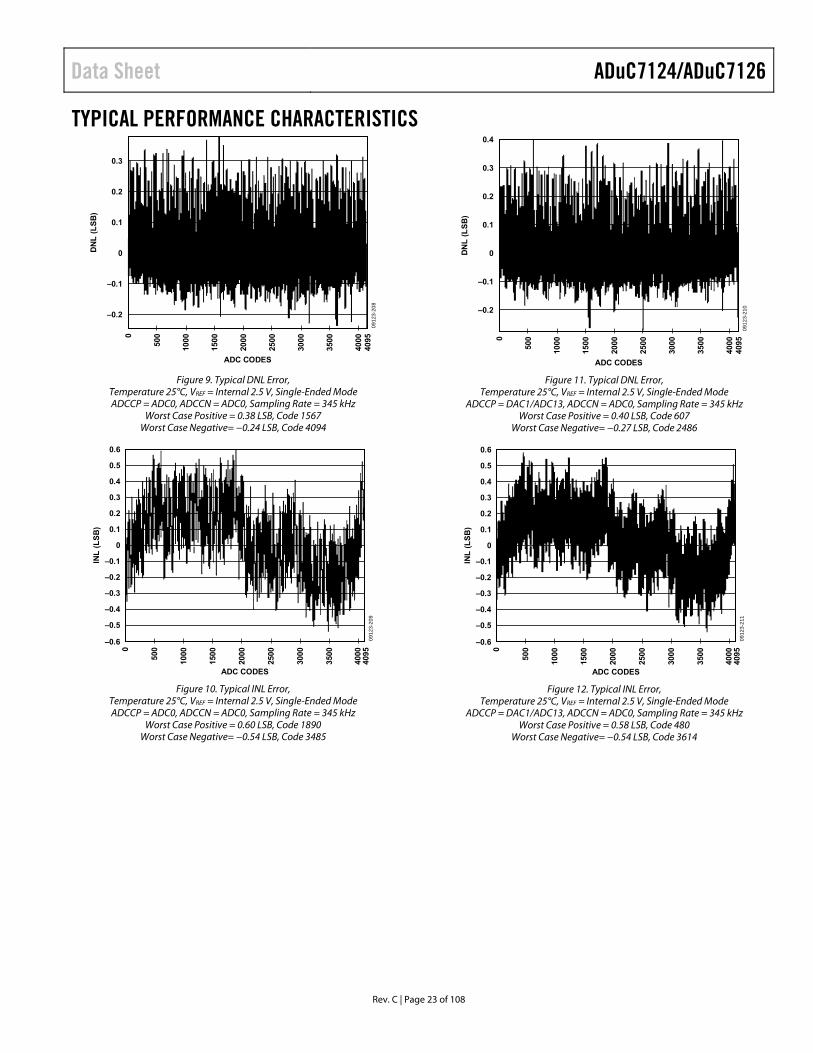
Figure 9. Typical DNL Error, Temperature 25°C, VREF = Internal 2.5 V, Single-Ended Mode ADCCP = ADC0, ADCCN = ADC0, Sampling Rate = 345 kHz
Worst Case Positive = 0.38 LSB, Code 1567 Worst Case Negative= −0.24 LSB, Code 4094
Figure 11. Typical DNL Error, Temperature 25°C, VREF = Internal 2.5 V, Single-Ended Mode
ADCCP = DAC1/ADC13, ADCCN = ADC0, Sampling Rate = 345 kHz Worst Case Positive = 0.40 LSB, Code 607
Worst Case Negative= −0.27 LSB, Code 2486
0.6
0.4
0.2
0
–0.2
–0.4
–0.5
0.5
0.3
0.1
–0.1
–0.3
–0.6
0
500
1000
3000
0912
3-20
9
INL
(LSB
)
ADC CODES
3500
4000
4095
1500
2000
2500
0.6
0.4
0.2
0
–0.2
–0.4
–0.5
0.5
0.3
0.1
–0.1
–0.3
–0.6 0912
3-21
1
INL
(LSB
)
0
500
1000
3000
ADC CODES
3500
4000
4095
1500
2000
2500
Figure 10. Typical INL Error,
Temperature 25°C, VREF = Internal 2.5 V, Single-Ended Mode ADCCP = ADC0, ADCCN = ADC0, Sampling Rate = 345 kHz
Worst Case Positive = 0.60 LSB, Code 1890 Worst Case Negative= −0.54 LSB, Code 3485
Figure 12. Typical INL Error, Temperature 25°C, VREF = Internal 2.5 V, Single-Ended Mode
ADCCP = DAC1/ADC13, ADCCN = ADC0, Sampling Rate = 345 kHz Worst Case Positive = 0.58 LSB, Code 480
Worst Case Negative= −0.54 LSB, Code 3614

ADuC7124/ADuC7126 Data Sheet
Rev. C | Page 24 of 108
0.3
0.4
0.2
0.1
0
–0.1
–0.2
–0.3 0912
3-21
2
DN
L (L
SB)
0
500
1000
3000
ADC CODES
3500
4000
4095
1500
2000
2500
Figure 13. Typical DNL Error,
Temperature 25°C, VREF = Internal 2.5 V, Single-Ended Mode ADCCP = ADC8, ADCCN = ADC0, Sampling Rate = 345 kHz
Worst-Case Positive = 0.42 LSB, Code 3583 Worst-Case Negative = −0.32 LSB, Code 3073
0.8
0.6
0
–0.2
–0.6
0.4
0.2
–0.4
–0.8 0912
3-21
3
INL
(LSB
)
0
500
1000
3000
ADC CODES
3500
4000
4095
1500
2000
2500
Figure 14. Typical INL Error, Temperature 25°C, VREF = Internal 2.5 V, Single-Ended Mode ADCCP = ADC8, ADCCN = ADC0, Sampling Rate = 345 kHz
Worst-Case Positive = 0.64 LSB, Code 802 Worst-Case Negative = −0.69 LSB, Code 3485
0.3
0.4
0.2
0.1
0
–0.1
–0.2
0912
3-21
4
DN
L (L
SB)
0
500
1000
3000
ADC CODES
3500
4000
4095
1500
2000
2500
Figure 15. Typical DNL Error,
Temperature 25°C, VREF = Internal 2.5 V, Single-Ended Mode ADCCP = DAC3/ADC15, ADCCN = ADC0, Sampling Rate = 345 kHz
Worst-Case Positive = 0.41 LSB, Code 2016 Worst-Case Negative = −0.26 LSB, Code 3841
0.6
0.4
0.2
0
–0.2
–0.4
–0.5
0.5
0.3
0.1
–0.1
–0.3
–0.6 0912
3-21
5
INL
(LSB
)
–0.6
0
500
1000
3000
ADC CODES
3500
4000
4095
1500
2000
2500
Figure 16. Typical INL Error, Temperature 25°C, VREF = Internal 2.5 V, Single-Ended Mode
ADCCP = DAC3/ADC15, ADCCN = ADC0, Sampling Rate = 345 kHz Worst-Case Positive = 0.55 LSB, Code 738
Worst-Case Negative = −0.68 LSB, Code 3230

Data Sheet ADuC7124/ADuC7126
Rev. C | Page 25 of 108
20
0
–20
–40
–60
–80
–100
–120
–1400 50 100 150 174.1
0912
3-21
6SIN
AD
, TH
D, A
ND
PH
SN O
F A
DC
(dB
)
FREQUENCY (kHz)
SNR: 69.85dBTHD: –79.91dBPHSN: –82.93dB, 29.771kHz
20
0
–20
–40
–60
–80
–100
–120
–1400 50 100 150 174.1
0912
3-21
9SIN
AD
, TH
D, A
ND
PH
SN O
F A
DC
(dB
)
FREQUENCY (kHz)
SNR: 65.97dBTHD: –78.63dBPHSN: –77.83dB, 146.6038kHz
Figure 17. SINAD, THD, and PHSN of ADC, VREF = Internal 2.5 V, Single-Ended Mode
ADCCP = ADC0
Figure 20. SINAD, THD, and PHSN of ADC, VREF = Internal 2.5 V, Single-Ended Mode ADCCP = ADC15/DAC3, ADCCN = ADC0
0.2
0.1
0
–0.1
–0.2
250
0912
3-22
0
DN
L (L
SB)
ADC CODES
500
750
1000
1250
1500
1750
2000
2250
2500
2750
3000
3250
3500
3750
4000
4095
DAC0DAC1
20
0
–20
–40
–60
–80
–100
–120
–1400 50 100 150 174.1
0912
3-21
7SIN
AD
, TH
D, A
ND
PH
SN O
F A
DC
(dB
)
FREQUENCY (kHz)
SNR: 67.10dBTHD: –79.79dBPHSN: –76.14dB, 54.9738kHz
Figure 21. DAC DNL Error, DAC0 Max Positive DNL: 0.188951, DAC1 Max Positive DNL: 0.190343
DAC0 Max Negative DNL: −0.120081, DAC1 Max Negative DNL: −0.15697
Figure 18. SINAD, THD, and PHSN of ADC, VREF = Internal 2.5 V, Single-Ended Mode ADCCP = DAC1/ADC13, ADCCN = ADC0
2.0
1.5
1.0
0.5
0
–0.5
–1.0
–1.5
–2.0
–2.5
250
0912
3-22
1
INL
(LSB
)
ADC CODES
500
750
1000
1250
1500
1750
2000
2250
2500
2750
3000
3250
3500
3750
4000
4095
DAC0DAC1
20
0
–20
–40
–60
–80
–100
–120
–1400 50 100 150 174.1
0912
3-21
8SIN
AD
, TH
D, A
ND
PH
SN O
F A
DC
(dB
)
FREQUENCY (kHz)
SNR: 67.44dBTHD: –82.33dBPHSN: –79.31dB, 54.9738kHz
Figure 22. DAC INL Error, DAC0 Max Positive INL: 1.84106, DAC1 Max Positive INL: 1.75312
DAC0 Max Negative INL: −0.887319, DAC1 Max Negative INL: −2.23708
Figure 19. SINAD, THD, and PHSN of ADC, VREF = Internal 2.5 V, Single-Ended Mode
ADCCP = ADC8, ADCCN = ADC0
ADuC7124/ADuC7126 Data Sheet
Rev. C | Page 26 of 108
TERMINOLOGY ADC SPECIFICATIONS Integral Nonlinearity (INL) The maximum deviation of any code from a straight line passing through the endpoints of the ADC transfer function. The endpoints of the transfer function are zero scale, a point ½ LSB below the first code transition, and full scale, a point ½ LSB above the last code transition.
Differential Nonlinearity (DNL) The difference between the measured and the ideal 1 LSB change between any two adjacent codes in the ADC.
Offset Error The deviation of the first code transition (0000…000) to (0000…001) from the ideal, that is, ½ LSB.
Gain Error The deviation of the last code transition from the ideal AIN voltage (full scale − 1.5 LSB) after the offset error has been adjusted out.
Signal to (Noise + Distortion) Ratio The measured ratio of signal to (noise + distortion) at the output of the ADC. The signal is the rms amplitude of the fundamental. Noise is the rms sum of all nonfundamental signals up to half the sampling frequency (fS/2), excluding dc.
The ratio is dependent upon the number of quantization levels in the digitization process; the more levels there are, the smaller the quantization noise becomes.
The theoretical signal to (noise + distortion) ratio for an ideal N-bit converter with a sine wave input is given by
Signal to (Noise + Distortion) = (6.02 N + 1.76) dB
Thus, for a 12-bit converter, this is 74 dB.
Total Harmonic Distortion The ratio of the rms sum of the harmonics to the fundamental.
DAC SPECIFICATIONS Relative Accuracy Otherwise known as endpoint linearity, relative accuracy is a measure of the maximum deviation from a straight line passing through the endpoints of the DAC transfer function. It is measured after adjusting for zero error and full-scale error.
Voltage Output Settling Time The amount of time it takes the output to settle to within a 1 LSB level for a full-scale input change.
Data Sheet ADuC7124/ADuC7126
Rev. C | Page 27 of 108
OVERVIEW OF THE ARM7TDMI CORE The ARM7® core is a 32-bit reduced instruction set computer (RISC). It uses a single 32-bit bus for instruction and data. The length of the data can be eight bits, 16 bits, or 32 bits. The length of the instruction word is 32 bits.
The ARM7TDMI is an ARM7 core with four additional features.
• T support for the Thumb® (16-bit) instruction set. • D support for debug. • M support for long multiplications. • I includes the EmbeddedICE module to support embedded
system debugging.
THUMB MODE (T) An ARM instruction is 32 bits long. The ARM7TDMI processor supports a second instruction set that has been compressed into 16 bits, called the Thumb instruction set. Faster execution from 16-bit memory and greater code density can usually be achieved by using the Thumb instruction set instead of the ARM instruction set, which makes the ARM7TDMI core particularly suitable for embedded applications.
However, the Thumb mode has two limitations:
• Thumb code typically requires more instructions for the same job. As a result, ARM code is usually best for maximizing the performance of time-critical code.
• The Thumb instruction set does not include some of the instructions needed for exception handling, which automatically switches the core to ARM code for exception handling.
See the ARM7TDMI user guide for details on the core architecture, the programming model, and both the ARM and ARM Thumb instruction sets.
LONG MULTIPLY (M) The ARM7TDMI instruction set includes four extra instruc-tions that perform 32-bit by 32-bit multiplication with a 64-bit result and 32-bit by 32-bit multiplication-accumulation (MAC) with a 64-bit result. These results are achieved in fewer cycles than required on a standard ARM7 core.
EmbeddedICE (I) EmbeddedICE provides integrated on-chip support for the core. The EmbeddedICE module contains the breakpoint and watch-point registers that allow code to be halted for debugging purposes. These registers are controlled through the JTAG test port.
When a breakpoint or watchpoint is encountered, the processor halts and enters debug state. Once in a debug state, the proces-sor registers can be inspected as well as the Flash/EE, SRAM, and memory mapped registers.
EXCEPTIONS ARM supports five types of exceptions and a privileged processing mode for each type. The five types of exceptions are
• Normal interrupt or IRQ. This is provided to service general-purpose interrupt handling of internal and external events.
• Fast interrupt or FIQ. This is provided to service data transfers or communication channels with low latency. FIQ has priority over IRQ.
• Memory abort. • Attempted execution of an undefined instruction. • Software interrupt instruction (SWI). This can be used to
make a call to an operating system.
Typically, the programmer defines an interrupt as IRQ, but for higher priority interrupt, that is, faster response time, the programmer can define an interrupt as FIQ.
ARM REGISTERS ARM7TDMI has a total of 37 registers: 31 general-purpose registers and six status registers. Each operating mode has dedicated banked registers.
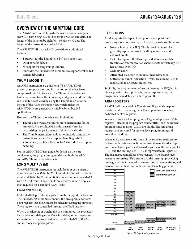
When writing user-level programs, 15 general-purpose, 32-bit registers (R0 to R14), the program counter (R15), and the current program status register (CPSR) are usable. The remaining registers are only used for system-level programming and exception handling.
When an exception occurs, some of the standard registers are replaced with registers specific to the exception mode. All excep-tion modes have replacement banked registers for the stack pointer (R13) and the link register (R14), as represented in Figure 23. The fast interrupt mode has more registers (R8 to R12) for fast interrupt processing. This means that the interrupt processing can begin without the need to save or restore these registers, and therefore, save critical time in the interrupt handling process.
0912
3-00
7
USABLE IN USER MODE
SYSTEM MODES ONLY
SPSR_UNDSPSR_IRQSPSR_ABTSPSR_SVC
R8_FIQR9_FIQ
R10_FIQR11_FIQR12_FIQR13_FIQR14_FIQ
R13_UNDR14_UND
R0R1R2R3R4R5R6R7R8R9
R10R11R12R13R14
R15 (PC)
R13_IRQR14_IRQ
R13_ABTR14_ABT
R13_SVCR14_SVC
SPSR_FIQCPSR
USER MODEFIQ
MODESVC
MODEABORTMODE
IRQMODE
UNDEFINEDMODE
Figure 23. Register Organization

ADuC7124/ADuC7126 Data Sheet
Rev. C | Page 28 of 108
More information relative to the model of the programmer and the ARM7TDMI core architecture can be found in the following materials from ARM:
• DDI0029G, ARM7TDMI Technical Reference Manual • DDI-0100, ARM Architecture Reference Manual
INTERRUPT LATENCY The worst-case latency for a fast interrupt request (FIQ) consists of the following:
• The longest time the request can take to pass through the synchronizer
• The time for the longest instruction to complete (the longest instruction is an LDM) that loads all the registers including the PC
• The time for the data abort entry • The time for the FIQ entry
At the end of this time, the ARM7TDMI executes the instruction at 0x1C (FIQ interrupt vector address). The maximum total time is 50 processor cycles, which is just under 1.2 μs in a system using a continuous 41.78 MHz processor clock.
The maximum interrupt request (IRQ) latency calculation is similar but must allow for the fact that FIQ has higher priority and can delay entry into the IRQ handling routine for an arbitrary length of time. This time can be reduced to 42 cycles if the LDM command is not used. Some compilers have an option to compile without using this command. Another option is to run the part in Thumb mode where the time is reduced to 22 cycles.
The minimum latency for FIQ or IRQ interrupts is a total of five cycles, which consist of the shortest time the request can take through the synchronizer plus the time to enter the exception mode.
Note that the ARM7TDMI always runs in ARM (32-bit) mode when in privileged modes, for example, when executing interrupt service routines.

Data Sheet ADuC7124/ADuC7126
Rev. C | Page 29 of 108
MEMORY ORGANIZATION The ADuC7124/ADuC7126 incorporate three separate blocks of memory: 32 kB of SRAM and two 64 kB blocks of on-chip Flash/EE memory. There are 126 kB of on-chip Flash/EE memory available to the user, and the remaining 2 kB are reserved for the system kernel. These blocks are mapped as shown in Figure 24.
Note that, by default, after a reset, the Flash/EE memory is mirrored at Address 0x00000000. It is possible to remap the SRAM at Address 0x00000000 by clearing Bit 0 of the REMAP MMR. This remap function is described in more detail in the Flash/EE memory chapter.
RESERVED
0x00080000
FLASH/EE
RESERVED0x00047FFF
0x00040000SRAM
0xFFFF0000
0xFFFFFFFFMMRs
0x0001FFFF
0x00000000
0x0009F800
RESERVED
REMAPPABLE MEMORY SPACE(FLASH/EE OR SRAM)
0912
3-02
5
Figure 24. Physical Memory Map
MEMORY ACCESS The ARM7 core sees memory as a linear array of a 232 byte location where the different blocks of memory are mapped as outlined in Figure 24.
The ADuC7124/ADuC7126 memory organization is configured in little endian format: the least significant byte is located in the lowest byte address and the most significant byte in the highest byte address.
BIT 31
BYTE 2
A62
.
.
.
BYTE 3
B73
.
.
.
BYTE 1
951
.
.
.
BYTE 0
840
.
.
.
BIT 0
32 BITS
0xFFFFFFFF
0x00000004
0x00000000
0912
3-02
6
Figure 25. Little Endian Format
FLASH/EE MEMORY The 128 kB of Flash/EE are organized as two banks of 32 kB × 16 bits. In the first block, 31 kB × 16 bits is user space and 1 kB × 16 bits is reserved for the factory-configured boot page. The page size of this Flash/EE memory is 512 bytes.
The second 64 kB block is organized in a similar manner. It is arranged in 32 kB × 16 bits. All of this is available as user space.
The 126 kB of Flash/EE are available to the user as code and nonvolatile data memory. There is no distinction between data and program because ARM code shares the same space. The real width of the Flash/EE memory is 16 bits, meaning that, in ARM mode (32-bit instruction), two accesses to the Flash/EE are necessary for each instruction fetch. Therefore, it is recom-mended that Thumb mode be used when executing from Flash/EE memory for optimum access speed. The maximum access speed for the Flash/EE memory is 41.78 MHz in Thumb mode and 20.89 MHz in full ARM mode (see the Execution Time from SRAM and Flash/EE section).
SRAM The 32 kB of SRAM are available to the user, organized as 8 kB × 32 bits, that is, 16 kB words. ARM code can run directly from SRAM at 41.78 MHz, given that the SRAM array is configured as a 32-bit wide memory array (see the Execution Time from SRAM and Flash/EE section).
MEMORY MAPPED REGISTERS The memory mapped register (MMR) space is mapped into the upper two pages of the memory array and accessed by indirect addressing through the ARM7 banked registers.
The MMR space provides an interface between the CPU and all on-chip peripherals. All registers except the core registers reside in the MMR area. All shaded locations shown in Figure 26 are unoccupied or reserved locations and should not be accessed by user software. Table 11 to Table 29 show the full MMR memory map.
The access time reading or writing a MMR depends on the advanced microcontroller bus architecture (AMBA) bus used to access the peripheral. The processor has two AMBA buses: the advanced high performance bus (AHB) used for system modules, and the advanced peripheral bus (APB) used for the lower performance peripheral. Access to the AHB is one cycle, and access to the APB is two cycles. All peripherals on the ADuC7124/ADuC7126 are on the APB except the Flash/EE memory and the GPIOs.
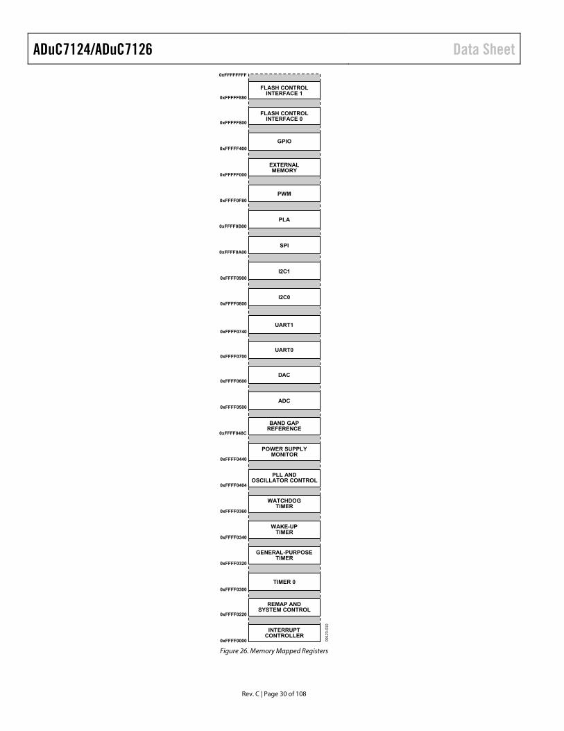
ADuC7124/ADuC7126 Data Sheet
Rev. C | Page 30 of 108
0912
3-01
0
FLASH CONTROLINTERFACE 0
FLASH CONTROLINTERFACE 1
GPIO
PLA
PWM
SPI
I2C1
I2C0
UART0
DAC
ADC
BAND GAPREFERENCE
POWER SUPPLYMONITOR
PLL ANDOSCILLATOR CONTROL
WATCHDOGTIMER
WAKE-UPTIMER
GENERAL-PURPOSETIMER
TIMER 0
REMAP ANDSYSTEM CONTROL
INTERRUPTCONTROLLER
0xFFFFFFFF
0xFFFFF800
0xFFFFF880
0xFFFFF400
0xFFFFF000
0xFFFF0F80
0xFFFF0B00
0xFFFF0A00
0xFFFF0900
0xFFFF0800
0xFFFF0700
UART10xFFFF0740
0xFFFF0600
0xFFFF0500
0xFFFF048C
0xFFFF0440
0xFFFF0404
0xFFFF0360
0xFFFF0340
0xFFFF0320
0xFFFF0300
0xFFFF0220
0xFFFF0000
EXTERNALMEMORY
Figure 26. Memory Mapped Registers

Data Sheet ADuC7124/ADuC7126
Rev. C | Page 31 of 108
Table 11. IRQ Base Address = 0xFFFF0000 Address Name Byte Access Type 0xFFFF0000 IRQSTA 4 R 0xFFFF0004 IRQSIG 4 R 0xFFFF0008 IRQEN 4 R/W 0xFFFF000C IRQCLR 4 W 0xFFFF0010 SWICFG 4 W 0xFFFF0014 IRQBASE 4 R/W 0xFFFF001C IRQVEC 4 R 0xFFFF0020 IRQP0 4 R/W 0xFFFF0024 IRQP1 4 R/W 0xFFFF0028 IRQP2 4 R/W 0xFFFF002C IRQP3 4 R/W 0xFFFF0030 IRQCONN 1 R/W 0xFFFF0034 IRQCONE 4 R/W 0xFFFF0038 IRQCLRE 1 W 0xFFFF003C IRQSTAN 1 R/W 0xFFFF0100 FIQSTA 4 R 0xFFFF0104 FIQSIG 4 R 0xFFFF0108 FIQEN 4 R/W 0xFFFF010C FIQCLR 4 W 0xFFFF011C FIQVEC 4 R 0xFFFF013C FIQSTAN 1 R/W
Table 12. System Control Base Address = 0xFFFF0200 Address Name Byte Access Type 0xFFFF0220 REMAP 1 R/W 0xFFFF0230 RSTSTA 1 R 0xFFFF0234 RSTCLR 1 W 0xFFFF0248 RSTKEY0 1 W 0xFFFF024C RSTCFG 1 R/W 0xFFFF0250 RSTKEY1 1 W
Table 13. Timer Base Address = 0xFFFF0300 Address Name Byte Access Type 0xFFFF0300 T0LD 2 R/W 0xFFFF0304 T0VAL 2 R 0xFFFF0308 T0CON 2 R/W 0xFFFF030C T0CLRI 1 W 0xFFFF0320 T1LD 4 R/W 0xFFFF0324 T1VAL 4 R 0xFFFF0328 T1CON 2 R/W 0xFFFF032C T1CLRI 1 W 0xFFFF0330 T1CAP 4 R/W 0xFFFF0340 T2LD 4 R/W 0xFFFF0344 T2VAL 4 R 0xFFFF0348 T2CON 2 R/W 0xFFFF034C T2CLRI 1 W 0xFFFF0360 T3LD 2 R/W 0xFFFF0364 T3VAL 2 R 0xFFFF0368 T3CON 2 R/W 0xFFFF036C T3CLRI 1 W

ADuC7124/ADuC7126 Data Sheet
Rev. C | Page 32 of 108
Table 14. PLL/PSM Base Address = 0xFFFF0400 Address Name Byte Access Type 0xFFFF0404 POWKEY1 2 W 0xFFFF0408 POWCON0 1 R/W 0xFFFF040C POWKEY2 2 W 0xFFFF0410 PLLKEY1 4 W 0xFFFF0414 PLLCON 1 R/W 0xFFFF0418 PLLKEY2 4 W 0xFFFF0434 POWKEY3 2 W 0xFFFF0438 POWCON1 2 R/W 0xFFFF043C POWKEY4 2 W
Table 15. PSM Base Address = 0xFFFF0440 Address Name Byte Access Type 0xFFFF0440 PSMCON 2 R/W 0xFFFF0444 CMPCON 2 R/W
Table 16. Reference Base Address = 0xFFFF0480 Address Name Byte Access Type 0xFFFF048C REFCON 1 R/W
Table 17. ADC Base Address = 0xFFFF0500 Address Name Byte Access Type 0xFFFF0500 ADCCON 2 R/W 0xFFFF0504 ADCCP 1 R/W 0xFFFF0508 ADCCN 1 R/W 0xFFFF050C ADCSTA 1 R 0xFFFF0510 ADCDAT 4 R 0xFFFF0514 ADCRST 1 R/W 0xFFFF0530 ADCGN 2 R/W 0xFFFF0534 ADCOF 2 R/W 0xFFFF0544 TSCON 1 R/W 0xFFFF0548 TEMPREF 2 R/W
Table 18. DAC Address Base = 0xFFFF0600 Address Name Byte Access Type 0xFFFF0600 DAC0CON 1 R/W 0xFFFF0604 DAC0DAT 4 R/W 0xFFFF0608 DAC1CON 1 R/W 0xFFFF060C DAC1DAT 4 R/W 0xFFFF0610 DAC2CON 1 R/W 0xFFFF0614 DAC2DAT 4 R/W 0xFFFF0618 DAC3CON 1 R/W 0xFFFF061C DAC3DAT 4 R/W 0xFFFF0650 DACBKEY1 2 W 0xFFFF0654 DACBCFG 1 R/W 0xFFFF0658 DACBKEY2 2 W
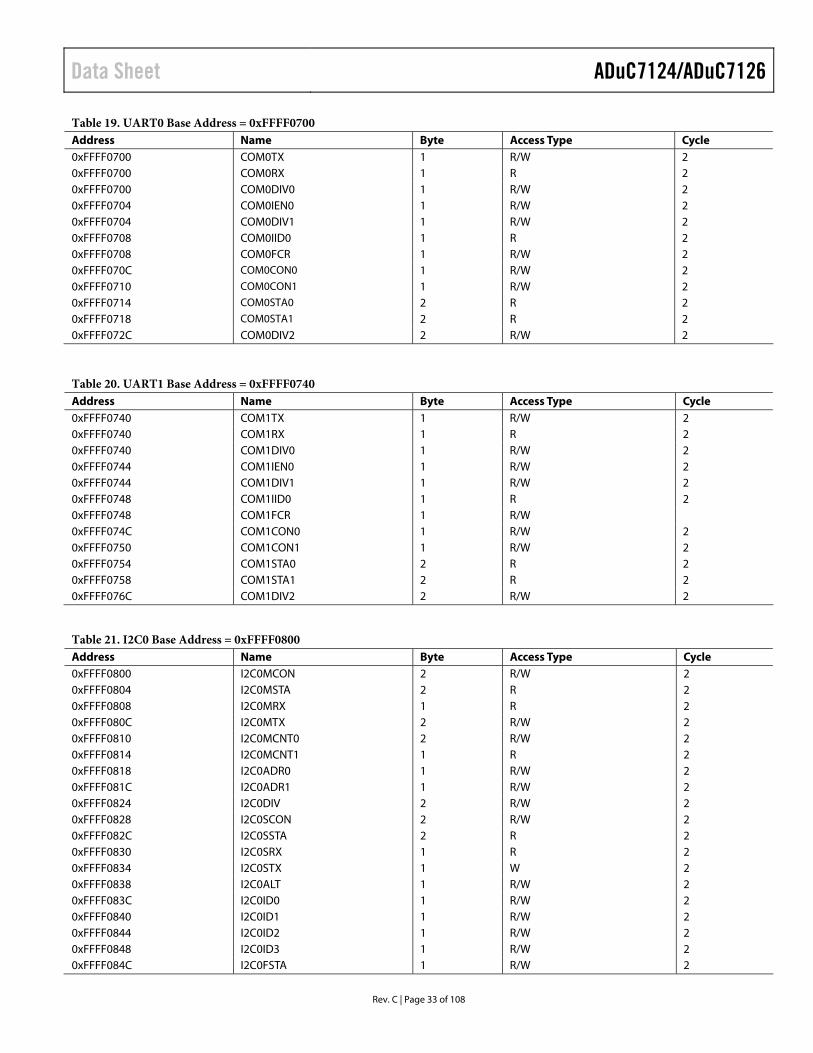
Data Sheet ADuC7124/ADuC7126
Rev. C | Page 33 of 108
Table 19. UART0 Base Address = 0xFFFF0700 Address Name Byte Access Type Cycle 0xFFFF0700 COM0TX 1 R/W 2 0xFFFF0700 COM0RX 1 R 2 0xFFFF0700 COM0DIV0 1 R/W 2 0xFFFF0704 COM0IEN0 1 R/W 2 0xFFFF0704 COM0DIV1 1 R/W 2 0xFFFF0708 COM0IID0 1 R 2 0xFFFF0708 COM0FCR 1 R/W 2 0xFFFF070C COM0CON0 1 R/W 2 0xFFFF0710 COM0CON1 1 R/W 2 0xFFFF0714 COM0STA0 2 R 2 0xFFFF0718 COM0STA1 2 R 2 0xFFFF072C COM0DIV2 2 R/W 2
Table 20. UART1 Base Address = 0xFFFF0740 Address Name Byte Access Type Cycle 0xFFFF0740 COM1TX 1 R/W 2 0xFFFF0740 COM1RX 1 R 2 0xFFFF0740 COM1DIV0 1 R/W 2 0xFFFF0744 COM1IEN0 1 R/W 2 0xFFFF0744 COM1DIV1 1 R/W 2 0xFFFF0748 COM1IID0 1 R 2 0xFFFF0748 COM1FCR 1 R/W 0xFFFF074C COM1CON0 1 R/W 2 0xFFFF0750 COM1CON1 1 R/W 2 0xFFFF0754 COM1STA0 2 R 2 0xFFFF0758 COM1STA1 2 R 2 0xFFFF076C COM1DIV2 2 R/W 2
Table 21. I2C0 Base Address = 0xFFFF0800 Address Name Byte Access Type Cycle 0xFFFF0800 I2C0MCON 2 R/W 2 0xFFFF0804 I2C0MSTA 2 R 2 0xFFFF0808 I2C0MRX 1 R 2 0xFFFF080C I2C0MTX 2 R/W 2 0xFFFF0810 I2C0MCNT0 2 R/W 2 0xFFFF0814 I2C0MCNT1 1 R 2 0xFFFF0818 I2C0ADR0 1 R/W 2 0xFFFF081C I2C0ADR1 1 R/W 2 0xFFFF0824 I2C0DIV 2 R/W 2 0xFFFF0828 I2C0SCON 2 R/W 2 0xFFFF082C I2C0SSTA 2 R 2 0xFFFF0830 I2C0SRX 1 R 2 0xFFFF0834 I2C0STX 1 W 2 0xFFFF0838 I2C0ALT 1 R/W 2 0xFFFF083C I2C0ID0 1 R/W 2 0xFFFF0840 I2C0ID1 1 R/W 2 0xFFFF0844 I2C0ID2 1 R/W 2 0xFFFF0848 I2C0ID3 1 R/W 2 0xFFFF084C I2C0FSTA 1 R/W 2
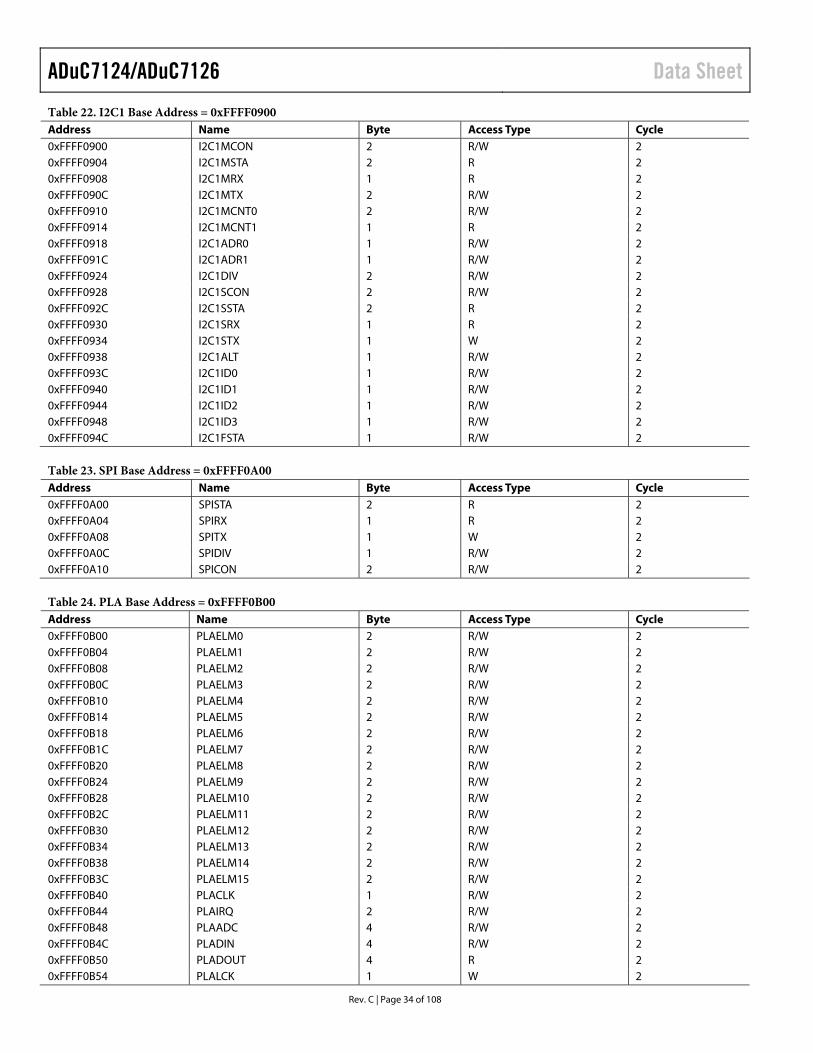
ADuC7124/ADuC7126 Data Sheet
Rev. C | Page 34 of 108
Table 22. I2C1 Base Address = 0xFFFF0900 Address Name Byte Access Type Cycle 0xFFFF0900 I2C1MCON 2 R/W 2 0xFFFF0904 I2C1MSTA 2 R 2 0xFFFF0908 I2C1MRX 1 R 2 0xFFFF090C I2C1MTX 2 R/W 2 0xFFFF0910 I2C1MCNT0 2 R/W 2 0xFFFF0914 I2C1MCNT1 1 R 2 0xFFFF0918 I2C1ADR0 1 R/W 2 0xFFFF091C I2C1ADR1 1 R/W 2 0xFFFF0924 I2C1DIV 2 R/W 2 0xFFFF0928 I2C1SCON 2 R/W 2 0xFFFF092C I2C1SSTA 2 R 2 0xFFFF0930 I2C1SRX 1 R 2 0xFFFF0934 I2C1STX 1 W 2 0xFFFF0938 I2C1ALT 1 R/W 2 0xFFFF093C I2C1ID0 1 R/W 2 0xFFFF0940 I2C1ID1 1 R/W 2 0xFFFF0944 I2C1ID2 1 R/W 2 0xFFFF0948 I2C1ID3 1 R/W 2 0xFFFF094C I2C1FSTA 1 R/W 2
Table 23. SPI Base Address = 0xFFFF0A00 Address Name Byte Access Type Cycle 0xFFFF0A00 SPISTA 2 R 2 0xFFFF0A04 SPIRX 1 R 2 0xFFFF0A08 SPITX 1 W 2 0xFFFF0A0C SPIDIV 1 R/W 2 0xFFFF0A10 SPICON 2 R/W 2
Table 24. PLA Base Address = 0xFFFF0B00 Address Name Byte Access Type Cycle 0xFFFF0B00 PLAELM0 2 R/W 2 0xFFFF0B04 PLAELM1 2 R/W 2 0xFFFF0B08 PLAELM2 2 R/W 2 0xFFFF0B0C PLAELM3 2 R/W 2 0xFFFF0B10 PLAELM4 2 R/W 2 0xFFFF0B14 PLAELM5 2 R/W 2 0xFFFF0B18 PLAELM6 2 R/W 2 0xFFFF0B1C PLAELM7 2 R/W 2 0xFFFF0B20 PLAELM8 2 R/W 2 0xFFFF0B24 PLAELM9 2 R/W 2 0xFFFF0B28 PLAELM10 2 R/W 2 0xFFFF0B2C PLAELM11 2 R/W 2 0xFFFF0B30 PLAELM12 2 R/W 2 0xFFFF0B34 PLAELM13 2 R/W 2 0xFFFF0B38 PLAELM14 2 R/W 2 0xFFFF0B3C PLAELM15 2 R/W 2 0xFFFF0B40 PLACLK 1 R/W 2 0xFFFF0B44 PLAIRQ 2 R/W 2 0xFFFF0B48 PLAADC 4 R/W 2 0xFFFF0B4C PLADIN 4 R/W 2 0xFFFF0B50 PLADOUT 4 R 2 0xFFFF0B54 PLALCK 1 W 2

Data Sheet ADuC7124/ADuC7126
Rev. C | Page 35 of 108
Table 25. PWM Base Address = 0xFFFF0F80 Address Name Byte Access Type Cycle 0xFFFF0F80 PWMCON0 2 R/W 2 0xFFFF0F84 PWM0COM0 2 R/W 2 0xFFFF0F88 PWM0COM1 2 R/W 2 0xFFFF0F8C PWM0COM2 2 R/W 2 0xFFFF0F90 PWM0LEN 2 R/W 2 0xFFFF0F94 PWM1COM0 2 R/W 2 0xFFFF0F98 PWM1COM1 2 R/W 2 0xFFFF0F9C PWM1COM2 2 R/W 2 0xFFFF0FA0 PWM1LEN 2 R/W 2 0xFFFF0FA4 PWM2COM0 2 R/W 2 0xFFFF0FA8 PWM2COM1 2 R/W 2 0xFFFF0FAC PWM2COM2 2 R/W 2 0xFFFF0FB0 PWM2LEN 2 R/W 2 0xFFFF0FB4 PWMCON1 2 R/W 2 0xFFFF0FB8 PWMCLRI 2 W 2
Table 26. External Memory Base Address = 0xFFFFF000 Address Name Byte Access Type Cycle 0xFFFFF000 XMCFG 1 R/W 2 0xFFFFF010 XM0CON 1 R/W 2 0xFFFFF014 XM1CON 1 R/W 2 0xFFFFF018 XM2CON 1 R/W 2 0xFFFFF01C XM3CON 1 R/W 2 0xFFFFF020 XM0PAR 2 R/W 2 0xFFFFF024 XM1PAR 2 R/W 2 0xFFFFF028 XM2PAR 2 R/W 2 0xFFFFF02C XM3PAR 2 R/W 2
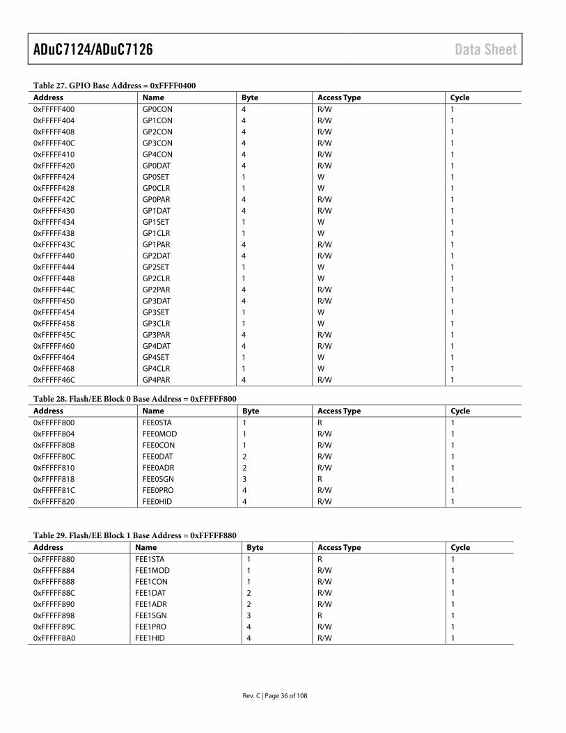
ADuC7124/ADuC7126 Data Sheet
Rev. C | Page 36 of 108
Table 27. GPIO Base Address = 0xFFFF0400 Address Name Byte Access Type Cycle 0xFFFFF400 GP0CON 4 R/W 1 0xFFFFF404 GP1CON 4 R/W 1 0xFFFFF408 GP2CON 4 R/W 1 0xFFFFF40C GP3CON 4 R/W 1 0xFFFFF410 GP4CON 4 R/W 1 0xFFFFF420 GP0DAT 4 R/W 1 0xFFFFF424 GP0SET 1 W 1 0xFFFFF428 GP0CLR 1 W 1 0xFFFFF42C GP0PAR 4 R/W 1 0xFFFFF430 GP1DAT 4 R/W 1 0xFFFFF434 GP1SET 1 W 1 0xFFFFF438 GP1CLR 1 W 1 0xFFFFF43C GP1PAR 4 R/W 1 0xFFFFF440 GP2DAT 4 R/W 1 0xFFFFF444 GP2SET 1 W 1 0xFFFFF448 GP2CLR 1 W 1 0xFFFFF44C GP2PAR 4 R/W 1 0xFFFFF450 GP3DAT 4 R/W 1 0xFFFFF454 GP3SET 1 W 1 0xFFFFF458 GP3CLR 1 W 1 0xFFFFF45C GP3PAR 4 R/W 1 0xFFFFF460 GP4DAT 4 R/W 1 0xFFFFF464 GP4SET 1 W 1 0xFFFFF468 GP4CLR 1 W 1 0xFFFFF46C GP4PAR 4 R/W 1
Table 28. Flash/EE Block 0 Base Address = 0xFFFFF800 Address Name Byte Access Type Cycle 0xFFFFF800 FEE0STA 1 R 1 0xFFFFF804 FEE0MOD 1 R/W 1 0xFFFFF808 FEE0CON 1 R/W 1 0xFFFFF80C FEE0DAT 2 R/W 1 0xFFFFF810 FEE0ADR 2 R/W 1 0xFFFFF818 FEE0SGN 3 R 1 0xFFFFF81C FEE0PRO 4 R/W 1 0xFFFFF820 FEE0HID 4 R/W 1
Table 29. Flash/EE Block 1 Base Address = 0xFFFFF880 Address Name Byte Access Type Cycle 0xFFFFF880 FEE1STA 1 R 1 0xFFFFF884 FEE1MOD 1 R/W 1 0xFFFFF888 FEE1CON 1 R/W 1 0xFFFFF88C FEE1DAT 2 R/W 1 0xFFFFF890 FEE1ADR 2 R/W 1 0xFFFFF898 FEE1SGN 3 R 1 0xFFFFF89C FEE1PRO 4 R/W 1 0xFFFFF8A0 FEE1HID 4 R/W 1

Data Sheet ADuC7124/ADuC7126
Rev. C | Page 37 of 108
ADC CIRCUIT OVERVIEW The analog-to-digital converter is a fast, multichannel, 12-bit ADC. It can operate from 2.7 V to 3.6 V supplies and is capable of providing a throughput of up to 1 MSPS when the clock source is 41.78 MHz. This block provides the user with a multichannel multiplexer, a differential track-and-hold, an on-chip reference, and an ADC.
The ADC consists of a 12-bit successive approximation con-verter based around two capacitor DACs. Depending on the input signal configuration, the ADC can operate in one of three different modes.
• Fully differential mode, for small and balanced signals • Single-ended mode, for any single-ended signals • Pseudo differential mode, for any single-ended signals,
taking advantage of the common-mode rejection offered by the pseudo differential input
The converter accepts an analog input range of 0 V to VREF when operating in single-ended or pseudo differential mode. In fully differential mode, the input signal must be balanced around a common-mode voltage (VCM) in the 0 V to AVDD range with a maximum amplitude of 2 × VREF (see Figure 27).
0912
3-01
1
AVDD
VCM
VCM
VCM
0
2VREF
2VREF
2VREF
Figure 27. Examples of Balanced Signals in Fully Differential Mode
A high precision, low drift, factory calibrated, 2.5 V reference is provided on chip. An external reference can also be connected as described in the Band Gap Reference section.
Single or continuous conversion modes can be initiated in the software. An external CONVSTART pin, an output generated from the on-chip PLA, or a Timer0 or Timer1 overflow can also be used to generate a repetitive trigger for ADC conversions.
A voltage output from an on-chip band gap reference propor-tional to absolute temperature can also be routed through the front-end ADC multiplexer, effectively an additional ADC channel input. This facilitates an internal temperature sensor channel that measures die temperature.
TRANSFER FUNCTION Pseudo Differential and Single-Ended Modes
In pseudo differential or single-ended mode, the input range is 0 V to VREF. The output coding is straight binary in pseudo differential and single-ended modes with
1 LSB = Full-Scale/4096, or 2.5 V/4096 = 0.61 mV, or 610 μV when VREF = 2.5 V
The ideal code transitions occur midway between successive integer LSB values (that is, ½ LSB, 3⁄2 LSB, 5⁄2 LSB, … , FS − 3/2 LSB). The ideal input/output transfer characteristic is shown in Figure 28.
0912
3-01
2
OU
TPU
T C
OD
E
VOLTAGE INPUT
1111 1111 1111
1111 1111 1110
1111 1111 1101
1111 1111 1100
0000 0000 0011
1LSB0V +FS – 1LSB
0000 0000 0010
0000 0000 0001
0000 0000 0000
1LSB =FULL-SCALE
4096
Figure 28. ADC Transfer Function in Pseudo Differential or Single-Ended Mode
Fully Differential Mode
The amplitude of the differential signal is the difference between the signals applied to the VIN+ and VIN– pins (that is, VIN+ – VIN–). VIN+ is selected by the ADCCP register, and VIN− is selected by the ADCCN register. The maximum amplitude of the differential signal is, therefore, –VREF to +VREF p-p (that is, 2 × VREF). This is regardless of the common mode (CM). The common mode is the average of the two signals, for example, (VIN+ + VIN–)/2, and is, therefore, the voltage that the two inputs are centered on. This results in the span of each input being CM ± VREF/2. This voltage must be set up externally, and its range varies with VREF (see the Driving the Analog Inputs section).
The output coding is twos complement in fully differential mode with 1 LSB = 2 × VREF/4096, or 2 × 2.5 V/4096 = 1.22 mV when VREF = 2.5 V. The output result is ±11 bits, but this is shifted by one to the right. This allows the result in ADCDAT to be declared as a signed integer when writing C code. The designed code transitions occur midway between successive integer LSB values (that is, ½ LSB, 3⁄2 LSB, 5⁄2 LSB, … , FS − 3⁄2 LSB). The ideal input/output transfer characteristic is shown in Figure 29.
0912
3-01
3
OU
TPU
T C
OD
E
VOLTAGE INPUT (VIN+ – VIN–)
0 1111 1111 1110
0 1111 1111 1100
0 1111 1111 1010
0 0000 0000 0010
0 0000 0000 0000
1 1111 1111 1110
1 0000 0000 0100
1 0000 0000 0010
1 0000 0000 0000–VREF + 1LSB +VREF – 1LSB0LSB
1LSB =2 × VREF
4096
SIGNBIT
Figure 29. ADC Transfer Function in Differential Mode

ADuC7124/ADuC7126 Data Sheet
Rev. C | Page 38 of 108
TYPICAL OPERATION Once configured via the ADC control and channel selection registers, the ADC converts the analog input and provides a 12-bit result in the ADC data register.
The top four bits are the sign bits. The 12-bit result is placed in Bit 16 to Bit 27 as shown in Figure 30. Again, it should be noted that in fully differential mode, the result is represented in twos complement format. In pseudo differential and single-ended modes, the result is represented in straight binary format.
0912
3-01
4
SIGN BITS 12-BIT ADC RESULT
31 27 16 15 0
Figure 30. ADC Result Format
The same format is used in DACxDAT, simplifying the software.
Current Consumption
The ADC in standby mode, that is, powered up but not converting, typically consumes 640 μA. The internal reference adds 140 μA. During conversion, the extra current is 0.3 μA multiplied by the sampling frequency (in kHz).
Timing
Figure 31 gives details of the ADC timing. The user controls the ADC clock speed and the number of acquisition clocks in the ADCCON MMR. By default, the acquisition time is eight clocks, and the clock divider is two. The number of extra clocks (such as bit trial or write) is set to 19, which gives a sampling rate of 774 kSPS. For conversion on temperature sensor, the ADC acquisition time is automatically set to 16 clocks, and the ADC clock divider is set to 32. When using multiple channels including the temperature sensor, the timing settings revert to the user-defined settings after reading the temperature sensor channel.
0912
3-01
5
ADC CLOCK
ACQ BIT TRIAL
DATA
ADCSTA = 0 ADCSTA = 1
ADC INTERRUPT
WRITE
CONVSTART
ADCBUSY
ADCDAT
Figure 31. ADC Timing
MMRS INTERFACE The ADC is controlled and configured via the eight MMRs.
ADCCON Register
Name: ADCCON
Address: 0xFFFF0500
Default Value: 0x0600
Access: Read/write
ADCCON is an ADC control register that allows the program-mer to enable the ADC peripheral, select the mode of operation of the ADC (either in single-ended mode, pseudo differential mode, or fully differential mode), and select the conversion type. This MMR is described in Table 30.
Table 30. ADCCON MMR Bit Descriptions Bit Value Description [15:14] Reserved. 13 Set by the user to enable edge trigger mode.
Cleared by the user to enable level trigger mode.
[12:10] ADC clock speed. 000 fADC/1. This divider is provided to obtain
1 MSPS ADC with an external clock <41.78 MHz. 001 fADC/2 (default value). 010 fADC/4. 011 fADC/8. 100 fADC/16. 101 fADC/32.
[9:8] ADC acquisition time. 00 Two clocks. 01 Four clocks. 10 Eight clocks (default value). 11 16 clocks.
7 Enable start conversion. Set by the user to start any type of
conversion command. Cleared by the user to disable a start conversion (clearing this bit does not stop the ADC when continuously converting).
6 Enable ADCBUSY. Set by the user to enable the ADCBUSY pin.
Cleared by the user to disable the ADCBUSY pin. 5 ADC power control. Set by the user to place the ADC in normal
mode (the ADC must be powered up for at least 5 μs before it converts correctly). Cleared by the user to place the ADC in power-down mode.
[4:3] Conversion mode. 00 Single-ended mode. 01 Differential mode. 10 Pseudo differential mode. 11 Reserved.
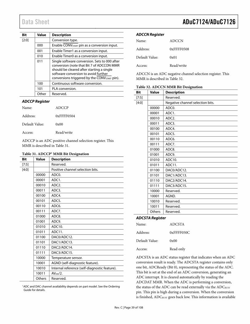
Data Sheet ADuC7124/ADuC7126
Rev. C | Page 39 of 108
Bit Value Description [2:0] Conversion type.
000 Enable CONVSTART pin as a conversion input.
001 Enable Timer1 as a conversion input. 010 Enable Timer0 as a conversion input. 011 Single software conversion. Sets to 000 after
conversion (note that Bit 7 of ADCCON MMR should be cleared after starting a single software conversion to avoid further conversions triggered by the CONVSTART pin).
100 Continuous software conversion. 101 PLA conversion. Other Reserved.
ADCCP Register
Name: ADCCP
Address: 0xFFFF0504
Default Value: 0x00
Access: Read/write
ADCCP is an ADC positive channel selection register. This MMR is described in Table 31.
Table 31. ADCCP1 MMR Bit Designation Bit Value Description [7:5] Reserved. [4:0] Positive channel selection bits. 00000 ADC0. 00001 ADC1. 00010 ADC2. 00011 ADC3. 00100 ADC4. 00101 ADC5. 00110 ADC6. 00111 ADC7. 01000 ADC8. 01001 ADC9. 01010 ADC10. 01011 ADC11. 01100 DAC0/ADC12. 01101 DAC1/ADC13. 01110 DAC2/ADC14. 01111 DAC3/ADC15. 10000 Temperature sensor. 10001 AGND (self-diagnostic feature). 10010 Internal reference (self-diagnostic feature). 10011 AVDD/2. Others Reserved.
1 ADC and DAC channel availability depends on part model. See the Ordering Guide for details.
ADCCN Register
Name: ADCCN
Address: 0xFFFF0508
Default Value: 0x01
Access: Read/write
ADCCN is an ADC negative channel selection register. This MMR is described in Table 32.
Table 32. ADCCN MMR Bit Designation Bit Value Description [7:5] Reserved. [4:0] Negative channel selection bits. 00000 ADC0. 00001 ADC1. 00010 ADC2. 00011 ADC3. 00100 ADC4. 00101 ADC5. 00110 ADC6. 00111 ADC7. 01000 ADC8. 01001 ADC9. 01010 ADC10. 01011 ADC11. 01100 DAC0/ADC12. 01101 DAC1/ADC13. 01110 DAC2/ADC14. 01111 DAC3/ADC15. 10000 Reserved. 10001 AGND. 10010 Reserved. 10011 Reserved. Others Reserved.
ADCSTA Register
Name: ADCSTA
Address: 0xFFFF050C
Default Value: 0x00
Access: Read only
ADCSTA is an ADC status register that indicates when an ADC conversion result is ready. The ADCSTA register contains only one bit, ADCReady (Bit 0), representing the status of the ADC. This bit is set at the end of an ADC conversion, generating an ADC interrupt. It is cleared automatically by reading the ADCDAT MMR. When the ADC is performing a conversion, the status of the ADC can be read externally via the ADCBUSY pin. This pin is high during a conversion. When the conversion is finished, ADCBUSY goes back low. This information is available
ADuC7124/ADuC7126 Data Sheet
Rev. C | Page 40 of 108
on P0.5 (see the General-Purpose Input/Output section) if enabled in the ADCCON register.
ADCDAT Register
Name: ADCDAT
Address: 0xFFFF0510
Default Value: 0x00000000
Access: Read only
ADCDAT is an ADC data result register that holds the 12-bit ADC result, as shown in Figure 30.
ADCRST Register
Name: ADCRST
Address: 0xFFFF0514
Default Value: 0x00
Access: Read/write
ADCRST resets the digital interface of the ADC. Writing any value to this register resets all the ADC registers to their default values.
ADCGN Register
Name: ADCGN
Address: 0xFFFF0530
Default Value: 0x0200
Access: Read/write
ADCGN is a 10-bit gain calibration register.
ADCOF Register
Name: ADCOF
Address: 0xFFFF0534
Default Value: 0x0200
Access: Read/write
ADCOF is a 10-bit offset calibration register.
CONVERTER OPERATION The ADC incorporates a successive approximation (SAR) architecture involving a charge-sampled input stage. This architecture can operate in three different modes: differential, pseudo differential, and single-ended.
Differential Mode
The ADuC7124/ADuC7126 each contains a successive approx-imation ADC based on two capacitive DACs. Figure 32 and Figure 33 show simplified schematics of the ADC in acquisition and conversion phases, respectively. The ADC comprises con-trol logic, a SAR, and two capacitive DACs. In Figure 32 (the acquisition phase), SW3 is closed and SW1 and SW2 are in
Position A. The comparator is held in a balanced condition, and the sampling capacitor arrays acquire the differential signal on the input.
0912
3-01
7
CAPACITIVEDAC
CAPACITIVEDAC
CONTROLLOGIC
COMPARATOR
SW3SW1
A
A
B
B
SW2
CS
CS
VREF
AIN0
AIN11
MUX
CHANNEL+
CHANNEL–
Figure 32. ADC Acquisition Phase
When the ADC starts a conversion, as shown in Figure 33, SW3 opens, and then SW1 and SW2 move to Position B. This causes the comparator to become unbalanced. Both inputs are discon-nected once the conversion begins. The control logic and the charge redistribution DACs are used to add and subtract fixed amounts of charge from the sampling capacitor arrays to bring the comparator back into a balanced condition. When the comparator is rebalanced, the conversion is complete. The control logic generates the ADC output code. The output impedances of the sources driving the VIN+ and VIN– pins must be matched; otherwise, the two inputs have different settling times, resulting in errors.
0912
3-01
8
CAPACITIVEDAC
CAPACITIVEDAC
CONTROLLOGIC
COMPARATOR
SW3SW1
A
A
B
B
SW2
CS
CS
VREF
AIN0
AIN11
MUX
CHANNEL+
CHANNEL–
Figure 33. ADC Conversion Phase
Pseudo Differential Mode
In pseudo differential mode, Channel− is linked to the ADCNEG pin of the ADuC7124/ADuC7126. In Figure 34, ADCNEG is represented as VIN−. SW2 switches between A (Channel−) and B (VREF). The ADCNEG pin must be connected to ground or to a low voltage. The input signal on VIN+ can then vary from VIN− to VREF + VIN−. Note that VIN− must be chosen so that VREF + VIN− do not exceed AVDD.
0912
3-01
9
CAPACITIVEDAC
CAPACITIVEDAC
CONTROLLOGIC
COMPARATOR
SW3SW1
A
A
B
B
SW2
CS
CS
VREF
AIN0
AIN11
VIN–
MUX
CHANNEL+
CHANNEL–
Figure 34. ADC in Pseudo Differential Mode

Data Sheet ADuC7124/ADuC7126
Rev. C | Page 41 of 108
Single-Ended Mode For ac applications, removing high frequency components from the analog input signal is recommended by using an RC low-pass filter on the relevant analog input pins. In applications where harmonic distortion and signal-to-noise ratio are critical, the analog input should be driven from a low impedance source. Large source impedances significantly affect the ac performance of the ADC. This can necessitate the use of an input buffer amplifier. The choice of the op amp is a function of the particular application. Figure 37 and Figure 38 give an example of the ADC front end.
In single-ended mode, SW2 is always connected internally to ground. The VIN− pin can be floating. The input signal range on VIN+ is 0 V to VREF.
0912
3-02
0
CAPACITIVEDAC
CAPACITIVEDAC
CONTROLLOGIC
COMPARATOR
SW3SW1A
B CS
CS
AIN0
AIN11
MUX
CHANNEL+
CHANNEL–
0912
3-06
1
ADuC7124/ADuC7126
ADC010Ω
0.01µF
Figure 35. ADC in Single-Ended Mode
Analog Input Structure Figure 37. Buffering Single-Ended/Pseudo Differential Input Figure 36 shows the equivalent circuit of the analog input structure
of the ADC. The four diodes provide ESD protection for the analog inputs. Care must be taken to ensure that the analog input signals never exceed the supply rails by more than 300 mV; this can cause these diodes to become forward-biased and start conducting into the substrate. These diodes can conduct up to 10 mA without causing irreversible damage to the part. 09
123-
062
ADuC7124/ADuC7126ADC0
VREF
ADC1
Figure 38. Buffering Differential Inputs
The C1 capacitors in Figure 36 are typically 4 pF and can be primarily attributed to pin capacitance. The resistors are lumped components made up of the on resistance of the switches. The value of these resistors is typically about 100 Ω. The C2 capacitors are the sampling capacitors of the ADC and typically have a capacitance of 16 pF.
When no amplifier is used to drive the analog input, the source impedance should be limited to values lower than 1 kΩ. The maximum source impedance depends on the amount of total harmonic distortion (THD) that can be tolerated. The THD increases as the source impedance increases and the performance degrades.
AVDD
C1
D
D
R1 C2
AVDD
C1
D
D
R1 C2
0912
3-02
1
DRIVING THE ANALOG INPUTS Internal or external references can be used for the ADC. In differential mode of operation, there are restrictions on the common-mode input signal (VCM), which is dependent upon the reference value and supply voltage used to ensure that the signal remains within the supply rails. Table 33 gives some calculated VCM minimum and VCM maximum values.
Figure 36. Equivalent Analog Input Circuit Conversion Phase: Switches Open, Track Phase: Switches Closed
Table 33. VCM Ranges AVDD VREF VCM Minimum VCM Maximum Signal Peak-to-Peak
2.5 V 1.25 V 2.05 V 2.5 V 2.048 V 1.024 V 2.276 V
3.3 V
1.25 V 0.75 V 2.55 V 2.048 V 1.25 V
2.5 V 1.25 V 1.75 V 2.5 V 2.048 V 1.024 V 1.976 V
3.0 V
1.25 V 0.75 V 2.25 V 2.048 V 1.25 V
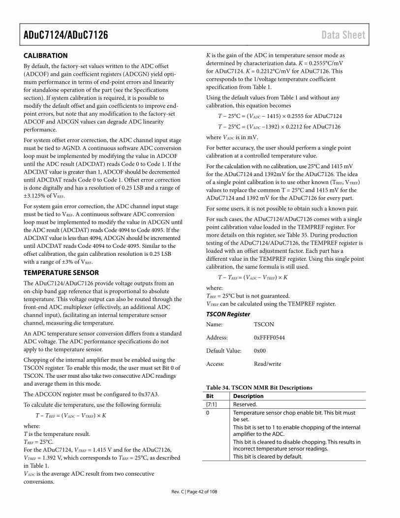
ADuC7124/ADuC7126 Data Sheet
Rev. C | Page 42 of 108
CALIBRATION By default, the factory-set values written to the ADC offset (ADCOF) and gain coefficient registers (ADCGN) yield opti-mum performance in terms of end-point errors and linearity for standalone operation of the part (see the Specifications section). If system calibration is required, it is possible to modify the default offset and gain coefficients to improve end-point errors, but note that any modification to the factory-set ADCOF and ADCGN values can degrade ADC linearity performance.
For system offset error correction, the ADC channel input stage must be tied to AGND. A continuous software ADC conversion loop must be implemented by modifying the value in ADCOF until the ADC result (ADCDAT) reads Code 0 to Code 1. If the ADCDAT value is greater than 1, ADCOF should be decremented until ADCDAT reads Code 0 to Code 1. Offset error correction is done digitally and has a resolution of 0.25 LSB and a range of ±3.125% of VREF.
For system gain error correction, the ADC channel input stage must be tied to VREF. A continuous software ADC conversion loop must be implemented to modify the value in ADCGN until the ADC result (ADCDAT) reads Code 4094 to Code 4095. If the ADCDAT value is less than 4094, ADCGN should be incremented until ADCDAT reads Code 4094 to Code 4095. Similar to the offset calibration, the gain calibration resolution is 0.25 LSB with a range of ±3% of VREF.
TEMPERATURE SENSOR The ADuC7124/ADuC7126 provide voltage outputs from an on-chip band gap reference that is proportional to absolute temperature. This voltage output can also be routed through the front-end ADC multiplexer (effectively, an additional ADC channel input), facilitating an internal temperature sensor channel, measuring die temperature.
An ADC temperature sensor conversion differs from a standard ADC voltage. The ADC performance specifications do not apply to the temperature sensor.
Chopping of the internal amplifier must be enabled using the TSCON register. To enable this mode, the user must set Bit 0 of TSCON. The user must also take two consecutive ADC readings and average them in this mode.
The ADCCON register must be configured to 0x37A3.
To calculate die temperature, use the following formula:
T – TREF = (VADC – VTREF) × K
where: T is the temperature result. TREF = 25°C. For the ADuC7124, VTREF = 1.415 V and for the ADuC7126, VTREF = 1.392 V, which corresponds to TREF = 25°C, as described in Table 1. VADC is the average ADC result from two consecutive conversions.
K is the gain of the ADC in temperature sensor mode as determined by characterization data. K = 0.2555°C/mV for ADuC7124. K = 0.2212°C/mV for ADuC7126. This corresponds to the 1/voltage temperature coefficient specification from Table 1.
Using the default values from Table 1 and without any calibration, this equation becomes
T − 25°C = (VADC − 1415) × 0.2555 for ADuC7124
T − 25°C = (VADC −1392) × 0.2212 for ADuC7126
where VADC is in mV.
For better accuracy, the user should perform a single point calibration at a controlled temperature value.
For the calculation with no calibration, use 25°C and 1415 mV for the ADuC7124 and 1392mV for the ADuC7126. The idea of a single point calibration is to use other known (TREF, VTREF) values to replace the common T = 25°C and 1415 mV for the ADuC7124 and 1392 mV for the ADuC7126 for every part.
For some users, it is not possible to obtain such a known pair.
For such cases, the ADuC7124/ADuC7126 comes with a single point calibration value loaded in the TEMPREF register. For more details on this register, see Table 35. During production testing of the ADuC7124/ADuC7126, the TEMPREF register is loaded with an offset adjustment factor. Each part has a different value in the TEMPREF register. Using this single point calibration, the same formula is still used.
T – TREF = (VADC – VTREF) × K
where: TREF = 25°C but is not guaranteed. VTREF can be calculated using the TEMPREF register.
TSCON Register
Name: TSCON
Address: 0xFFFF0544
Default Value: 0x00
Access: Read/write
Table 34. TSCON MMR Bit Descriptions Bit Description [7:1] Reserved. 0 Temperature sensor chop enable bit. This bit must
be set. This bit is set to 1 to enable chopping of the internal
amplifier to the ADC. This bit is cleared to disable chopping. This results in
incorrect temperature sensor readings. This bit is cleared by default.

Data Sheet ADuC7124/ADuC7126
Rev. C | Page 43 of 108
TEMPREF Register
Name: TEMPREF
Address: 0xFFFF0548
Default Value: 0xXXXX
Access: Read/write
Table 35. TEMPREF MMR Bit Descriptions Bit Description [15:9] Reserved. 8 Temperature reference voltage sign bit. [7:0] Temperature sensor offset calibration voltage.
To calculate the VTEMP from the TEMPREF register, perform the following calculation: If TEMPREF sign is negative,
CTREF = 2292 − TEMPREF[7:0] where TEMPREF[8] = 1 Or If TEMPREF sign is positive,
CTREF = TEMPREF[7:0] + 2292 where TEMPREF[8] = 0. Finally,
VTREF = ((CTREF × VREF)/4096) × 1000 Insert VTREF into
T − TREF = (VADC − VTREF) × K Note that the ADC Code Value 2292 is a default value when using the TEMPREF register. It is not an exact value and must only be used with the TEMPREF register.
BAND GAP REFERENCE Each ADuC7124/ADuC7126 provides on-chip band gap references of 2.5 V, which can be used for the ADC and DAC. This internal reference also appears on the VREF pin. When using the internal reference, a 0.47 μF capacitor must be connected from the external VREF pin to AGND to ensure stability and fast
response during ADC conversions. This reference can also be connected to an external pin (VREF) and used as a reference for other circuits in the system. An external buffer is required because of the low drive capability of the VREF output (<5 μA). A programmable option also allows an external reference input on the VREF pin. Note that it is not possible to disable the internal reference. Therefore, the external reference source must be capable of overdriving the internal reference source.
REFCON Register
Name: REFCON
Address: 0xFFFF048C
Default Value: 0x00
Access: Read/write
The band gap reference interface consists of an 8-bit MMR REFCON, described in Table 36.
Table 36. REFCON MMR Bit Descriptions Bit Description [7:2] Reserved. 1 Internal reference power-down bit.
Set this bit to 1 to power down the internal reference source. This bit should be set when connecting an external reference source. Clear this bit to enable the internal reference. This bit is cleared by default.
0 Internal reference output enable. Set by the user to connect the internal 2.5 V reference to the VREF pin. The reference can be used for an external component but must be buffered. Cleared by the user to disconnect the reference from the VREF pin.
To connect an external reference source to the ADuC7124/ ADuC7126, configure REFCON = 0x00. ADC and the DACs can be configured to use same or a different reference resource (see Table 66).

ADuC7124/ADuC7126 Data Sheet
Rev. C | Page 44 of 108
NONVOLATILE FLASH/EE MEMORY The ADuC7124/ADuC7126 incorporate Flash/EE memory technology on-chip to provide the user with nonvolatile, in-circuit reprogrammable memory space.
Like EEPROM, flash memory can be programmed in-system at a byte level, although it must first be erased. The erase is performed in page blocks. As a result, flash memory is often and more correctly referred to as Flash/EE memory.
Overall, Flash/EE memory represents a step closer to the ideal memory device that includes nonvolatility, in-circuit programmability, high density, and low cost. Incorporated in the ADuC7124/ADuC7126, Flash/EE memory technology allows the user to update program code space in-circuit, without the need to replace one-time programmable (OTP) devices at remote operating nodes.
Flash/EE Memory
The ADuC7124/ADuC7126 contain two 64 kB arrays of Flash/EE memory. In the first block, the lower 62 kB is available to the user, and the upper 2 kB of this Flash/EE program memory array contain permanently embedded firmware, allowing in-circuit serial download. The 2 kB of embedded firmware also contain a power-on configuration routine that downloads factory cali-brated coefficients to the various calibrated peripherals (band gap references and so on). This 2 kB embedded firmware is hidden from user code. It is not possible for the user to read, write, or erase this page. In the second block, all 64 kB of Flash/EE memory are available to the user.
The 126 kB of Flash/EE memory can be programmed in-circuit, using the serial download mode or the JTAG mode provided.
Flash/EE Memory Reliability
The Flash/EE memory arrays on the parts are fully qualified for two key Flash/EE memory characteristics: Flash/EE memory cycling endurance and Flash/EE memory data retention.
Endurance quantifies the ability of the Flash/EE memory to be cycled through many program, read, and erase cycles. A single endurance cycle is composed of four independent, sequential events, defined as
1. Initial page erase sequence. 2. Read/verify sequence (single Flash/EE). 3. Byte program sequence memory. 4. Second read/verify sequence (endurance cycle).
In reliability qualification, every half word (16-bit wide) location of the three pages (top, middle, and bottom) in the Flash/EE memory is cycled 10,000 times from 0x0000 to 0xFFFF. As indicated in Table 1, the Flash/EE memory endurance qualification is carried out in accordance with JEDEC Retention Lifetime Specification A117 over the industrial temperature range of −40° to +125°C. The results allow the specification of a minimum endurance figure over a supply temperature of 10,000 cycles.
Retention quantifies the ability of the Flash/EE memory to retain its programmed data over time. Again, the parts are qualified in accordance with the formal JEDEC Retention Lifetime Specification (A117) at a specific junction temperature (TJ = 85°C). As part of this qualification procedure, the Flash/EE memory is cycled to its specified endurance limit (see the Flash/EE Memory section) before data retention is character-ized. This means that the Flash/EE memory is guaranteed to retain its data for its fully specified retention lifetime every time the Flash/EE memory is reprogrammed. In addition, note that retention lifetime, based on the activation energy of 0.6 eV, derates with TJ as shown in Figure 39.
150
300
450
600
30 40 55 70 85 100 125 135 150
RET
ENTI
ON
(Yea
rs)
0 0912
3-08
5
JUNCTION TEMPERATURE (°C)
Figure 39. Flash/EE Memory Data Retention
PROGRAMMING The 62 kB of Flash/EE memory can be programmed in-circuit, using the serial download mode or the provided JTAG mode.
Serial Downloading (In-Circuit Programming)
The ADuC7124/ADuC7126 facilitate code download via the standard UART serial port. It is only available on UART0 (P01.0 & P1.1). The parts enter serial download mode after a reset or power cycle if the BM pin is pulled low through an external 1 kΩ resistor. When in serial download mode, the user can download code to the full 126 kB of Flash/EE memory while the device is in-circuit in its target application hardware. An executable PC serial download is provided as part of the development system for serial downloading via the UART. The AN-724 application note describes the UART download protocol.
Downloading (In-Circuit Programming) via I2C
The ADuC7126BSTZ126I and ADuC7126BSTZ126IRL models facilitate code download via the the I2C port. The models enter download mode after a reset or power cycle if the BM pin is pulled low through an external 1 kΩ resistor and Flash Address 0x80014 = 0xFFFFFFFF. Once in download mode, the user can download code to the full 126 kB of Flash/EE memory while the device is in-circuit in its target application hardware. An executable PC I2C download is provided as part of the development system

Data Sheet ADuC7124/ADuC7126
Rev. C | Page 45 of 108
for serial downloading via the I2C. A USB-to-I2C download dongle can be purchased from Analog Devices, Inc. This board connects to the USB port of a PC and to the I2C port of the ADuC7126. The part number is USB-I2C/LIN-CONV-Z.
The AN-806 Application Note describes the protocol for serial downloading via the I2C in more detail.
JTAG Access
The JTAG protocol uses the on-chip JTAG interface to facilitate code download and debug.
To access the part via the JTAG interface, the P0.0/BM pin must be set high.
When debugging, user code should not write to the P0.1, P0.2, and P0.3 pins. If user code toggles any of these pins, JTAG debug pods are not able to connect to the ADuC7124/ADuC7126. If this happens, mass erase the part using the UART/I2C downloader.
FLASH/EE MEMORY SECURITY The 126 kB of Flash/EE memory available to the user can be read and write protected. Bit 31 of the FEE0PRO/FEE0HID MMR protects the 126 kB from being read through JTAG and in UART programming mode. The other 31 bits of this register protect writing to the Flash/EE memory; each bit protects four pages, that is, 2 kB. Write protection is activated for all access types. FEE1PRO and FEE1HID, similarly, protect the second 64 kB block. All 32 bits of this are used to protect four pages at a time.
Three Levels of Protection
• Protection can be set and removed by writing directly into FEExHID MMR. This protection does not remain after reset.
• Protection can be set by writing into FEExPRO MMR. It takes effect only after a save protection command (0x0C) and a reset. The FEExPRO MMR is protected by a key to avoid direct access. The key is saved once and must be entered again to modify FEExPRO. A mass erase sets the key back to 0xFFFF but also erases all the user code.
• Flash can be permanently protected by using the FEExPRO MMR and a particular key value of 0xDEADDEAD. Entering the key again to modify the FEExPRO register is not allowed.
Sequence to Write the Key
1. Write the bit in FEExPRO corresponding to the page to be protected.
2. Enable key protection by setting Bit 6 of FEExMOD (Bit 5 must equal 0).
3. Write a 32-bit key in FEExADR and FEExDAT. 4. Run the write key command 0x0C in FEExCON; wait for
the read to be successful by monitoring FEExSTA. 5. Reset the part.
To remove or modify the protection, the same sequence is used with a modified value of FEExPRO. If the key chosen is the
value 0xDEAD, the memory protection cannot be removed. Only a mass erase unprotects the part, but it also erases all user code.
The sequence to write the key is illustrated in the following example (this protects writing Page 4 to Page 7 of the Flash):
FEExPRO=0xFFFFFFFD; //Protect Page 4 to Page 7 FEExMOD=0x48; //Write key enable FEExADR=0x1234; //16 bit key value FEExDAT=0x5678; //16 bit key value FEExCON= 0x0C; //Write key command
The same sequence should be followed to protect the part permanently with FEExADR = 0xDEAD and FEExDAT = 0xDEAD.
FLASH/EE CONTROL INTERFACE
Table 37. FEE0STA Register Name Address Default Value Access FEE0STA 0xFFFFF800 0x0000 R
Table 38. FEE0MOD Register Name Address Default Value Access FEE0MOD 0xFFFFF804 0x80 R/W
Table 39. FEE0CON Register Name Address Default Value Access FEE0CON 0xFFFFF808 0x00 R/W
Table 40. FEE0DAT Register Name Address Default Value Access FEE0DAT 0xFFFFF80C 0xXXXX R/W
FEE0DAT is a 16-bit data register.
Table 41. FEE0ADR Register Name Address Default Value Access FEE0ADR 0xFFFFF810 0x0000 R/W
FEE0ADR is a 16-bit address register.
Table 42. FEE0SGN Register Name Address Default Value Access FEE0SGN 0xFFFFF818 0xFFFFFF R
FEE0SGN is a 24-bit code signature.
Table 43. FEE0PRO Register Name Address Default Value Access FEE0PRO 0xFFFFF81C 0x00000000 R/W
FEE0PRO provides protection following subsequent reset MMR. It requires a software key (see Table 56).
Table 44. FEE0HID Register Name Address Default Value Access FEE0HID 0xFFFFF820 0xFFFFFFFF R/W
FEE0HID provides immediate protection MMR. It does not require any software keys (see Table 56).

ADuC7124/ADuC7126 Data Sheet
Rev. C | Page 46 of 108
Table 45. FEE1STA Register Name Address Default Value Access FEE1STA 0xFFFFF880 0x0000 R
Table 46. FEE1MOD Register Name Address Default Value Access FEE1MOD 0xFFFFF884 0x80 R/W
Table 47. FEE1CON Register Name Address Default Value Access FEE1CON 0xFFFFF888 0x00 R/W
Table 48. FEE1DAT Register Name Address Default Value Access FEE1DAT 0xFFFFF88C 0xXXXX R/W
FEE1DAT is a 16-bit data register.
Table 49. FEE1ADR Register Name Address Default Value Access FEE1ADR 0xFFFFF890 0x0000 R/W
FEE1ADR is a 16-bit address register.
Table 50. FEE1SGN Register Name Address Default Value Access FEE1SGN 0xFFFFF898 0xFFFFFF R
FEE1SGN is a 24-bit code signature.
Table 51. FEE1PRO Register Name Address Default Value Access FEE1PRO 0xFFFFF89C 0x00000000 R/W
FEE1PRO provides protection following subsequent reset MMR. It requires a software key (see Table 57).
Table 52. FEE1HID Register Name Address Default Value Access FEE1HID 0xFFFFF8A0 0xFFFFFFFF R/W
FEE1HID provides immediate protection MMR. It does not require any software keys (see Table 57).
Command Sequence for Executing a Mass Erase
FEE0DAT = 0x3CFF; FEE0ADR = 0xFFC3; FEE0MOD = FEE0MOD|0x8; //Erase key enable FEE0CON = 0x06; //Mass erase command
Table 53. FEExSTA MMR Bit Descriptions Bit Description [15:6] Reserved. 5 Reserved. 4 Reserved. 3 Flash/EE interrupt status bit.
Set automatically when an interrupt occurs, that is, when a command is complete and the Flash/EE interrupt enable bit in the FEExMOD register is set. Cleared when reading the FEExSTA register.
2 Flash/EE controller busy. Set automatically when the controller is busy. Cleared automatically when the controller is not busy.
1 Command fail. Set automatically when a command completes unsuccessfully. Cleared automatically when reading the FEExSTA register.
0 Command complete. Set by MicroConverter when a command is complete. Cleared automatically when reading the FEExSTA register.

Data Sheet ADuC7124/ADuC7126
Rev. C | Page 47 of 108
Table 54. FEExMOD MMR Bit Descriptions Bit Description [7:5] Reserved. 4 Flash/EE interrupt enable.
Set by the user to enable the Flash/EE interrupt. The interrupt occurs when a command is complete. Cleared by the user to disable the Flash/EE interrupt.
3 Erase/write command protection. Set by the user to enable the erase and write commands. Cleared to protect the Flash/EE memory against the erase/write command.
2 Reserved. Should always be set to 0 by the user. [1:0] Flash/EE wait states. Both Flash/EE blocks must have the same wait state value for any change to take effect.
Table 55. Command Codes in FEExCON Code Command Description 0x001 Null Idle state. 0x011
Single read Load FEExDAT with the 16-bit data indexed by FEExADR. 0x021
Single write Write FEExDAT at the address pointed to by FEExADR. This operation takes 50 μs. 0x031
Erase/write Erase the page indexed by FEExADR and write FEExDAT at the location pointed to by FEExADR. This operation takes 20 ms.
0x041 Single verify Compare the contents of the location pointed to by FEExADR to the data in FEExDAT. The result of the
comparison is returned in FEExSTA, Bit 1. 0x051
Single erase Erase the page indexed by FEExADR. 0x061
Mass erase Erase user space. The 2 kB of kernel are protected in Block 0. This operation takes 2.48 sec. To prevent accidental execution, a command sequence is required to execute this instruction.
0x07 Reserved Reserved. 0x08 Reserved Reserved. 0x09 Reserved Reserved. 0x0A Reserved Reserved. 0x0B Signature Gives a signature of the 64 kB of Flash/EE in the 24-bit FEExSIGN MMR. This operation takes 32,778 clock cycles. 0x0C Protect This command can be run only once. The value of FEExPRO is saved and can be removed only with a mass erase
(0x06) or with the key. 0x0D Reserved Reserved. 0x0E Reserved Reserved. 0x0F Ping No operation, interrupt generated. 1 The FEExCON register always reads 0x07 immediately after execution of any of these commands.
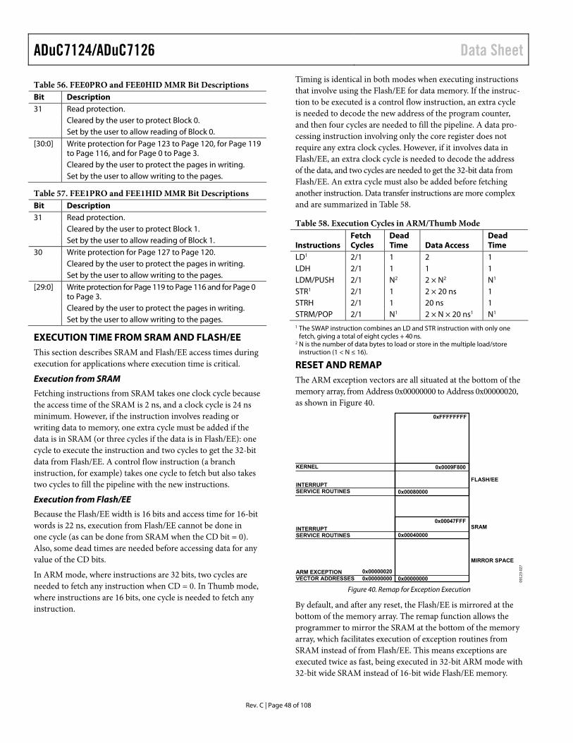
ADuC7124/ADuC7126 Data Sheet
Rev. C | Page 48 of 108
Table 56. FEE0PRO and FEE0HID MMR Bit Descriptions Bit Description 31 Read protection. Cleared by the user to protect Block 0. Set by the user to allow reading of Block 0. [30:0] Write protection for Page 123 to Page 120, for Page 119
to Page 116, and for Page 0 to Page 3. Cleared by the user to protect the pages in writing. Set by the user to allow writing to the pages.
Table 57. FEE1PRO and FEE1HID MMR Bit Descriptions Bit Description 31 Read protection. Cleared by the user to protect Block 1. Set by the user to allow reading of Block 1. 30 Write protection for Page 127 to Page 120. Cleared by the user to protect the pages in writing. Set by the user to allow writing to the pages. [29:0] Write protection for Page 119 to Page 116 and for Page 0
to Page 3. Cleared by the user to protect the pages in writing. Set by the user to allow writing to the pages.
EXECUTION TIME FROM SRAM AND FLASH/EE This section describes SRAM and Flash/EE access times during execution for applications where execution time is critical.
Execution from SRAM
Fetching instructions from SRAM takes one clock cycle because the access time of the SRAM is 2 ns, and a clock cycle is 24 ns minimum. However, if the instruction involves reading or writing data to memory, one extra cycle must be added if the data is in SRAM (or three cycles if the data is in Flash/EE): one cycle to execute the instruction and two cycles to get the 32-bit data from Flash/EE. A control flow instruction (a branch instruction, for example) takes one cycle to fetch but also takes two cycles to fill the pipeline with the new instructions.
Execution from Flash/EE
Because the Flash/EE width is 16 bits and access time for 16-bit words is 22 ns, execution from Flash/EE cannot be done in one cycle (as can be done from SRAM when the CD bit = 0). Also, some dead times are needed before accessing data for any value of the CD bits.
In ARM mode, where instructions are 32 bits, two cycles are needed to fetch any instruction when CD = 0. In Thumb mode, where instructions are 16 bits, one cycle is needed to fetch any instruction.
Timing is identical in both modes when executing instructions that involve using the Flash/EE for data memory. If the instruc-tion to be executed is a control flow instruction, an extra cycle is needed to decode the new address of the program counter, and then four cycles are needed to fill the pipeline. A data pro-cessing instruction involving only the core register does not require any extra clock cycles. However, if it involves data in Flash/EE, an extra clock cycle is needed to decode the address of the data, and two cycles are needed to get the 32-bit data from Flash/EE. An extra cycle must also be added before fetching another instruction. Data transfer instructions are more complex and are summarized in Table 58.
Table 58. Execution Cycles in ARM/Thumb Mode
Instructions Fetch Cycles
Dead Time Data Access
Dead Time
LD1 2/1 1 2 1 LDH 2/1 1 1 1 LDM/PUSH 2/1 N2 2 × N2 N1 STR1 2/1 1 2 × 20 ns 1 STRH 2/1 1 20 ns 1 STRM/POP 2/1 N1 2 × N × 20 ns1 N1 1 The SWAP instruction combines an LD and STR instruction with only one
fetch, giving a total of eight cycles + 40 ns. 2 N is the number of data bytes to load or store in the multiple load/store
instruction (1 < N ≤ 16).
RESET AND REMAP The ARM exception vectors are all situated at the bottom of the memory array, from Address 0x00000000 to Address 0x00000020, as shown in Figure 40.
KERNEL
INTERRUPTSERVICE ROUTINES
INTERRUPTSERVICE ROUTINES
ARM EXCEPTIONVECTOR ADDRESSES
0x00000020
0x00047FFF
0x0009F800
0xFFFFFFFF
FLASH/EE
SRAM
MIRROR SPACE
0x00000000 0x00000000
0x00040000
0x00080000
0912
3-02
7
Figure 40. Remap for Exception Execution
By default, and after any reset, the Flash/EE is mirrored at the bottom of the memory array. The remap function allows the programmer to mirror the SRAM at the bottom of the memory array, which facilitates execution of exception routines from SRAM instead of from Flash/EE. This means exceptions are executed twice as fast, being executed in 32-bit ARM mode with 32-bit wide SRAM instead of 16-bit wide Flash/EE memory.

Data Sheet ADuC7124/ADuC7126
Rev. C | Page 49 of 108
Table 59. REMAP MMR Bit Descriptions (Address = 0xFFFF0220. Default Value = 0x00) Bit Name Description 0 Remap Remap bit.
Set by the user to remap the SRAM to Address 0x00000000. Cleared automatically after reset to remap the Flash/EE memory to Address 0x00000000.
Remap Operation
When a reset occurs on the ADuC7124/ADuC7126, execution automatically starts in factory programmed, internal configuration code. This kernel is hidden and cannot be accessed by user code. If the part is in normal mode (BM pin is high), it executes the power-on configuration routine of the kernel and then jumps to the reset vector address, 0x00000000, to execute the reset exception routine of the user.
Because the Flash/EE is mirrored at the bottom of the memory array at reset, the reset interrupt routine must always be written in Flash/EE.
The remap is done from Flash/EE by setting Bit 0 of the REMAP register. Caution must be taken to execute this command from Flash/EE, above Address 0x00080020, and not from the bottom of the array, because this is replaced by the SRAM.
This operation is reversible. The Flash/EE can be remapped at Address 0x00000000 by clearing Bit 0 of the REMAP MMR. Caution must again be taken to execute the remap function from outside the mirrored area. Any type of reset remaps the Flash/EE memory at the bottom of the array.
Reset Operation
There are four kinds of reset: external, power-on, watchdog expiation, and software force. The RSTSTA register indicates the source of the last reset, and RSTCLR allows clearing of the RSTSTA register. These registers can be used during a reset exception service routine to identify the source of the reset. If RSTSTA is null, the reset is external.
The RSTCFG register allows different peripherals to retain their state after a watchdog or software reset.
RSTSTA Register
Name: RSTSTA
Address: 0xFFFF0230
Default Value: 0x01
Access: Read only
Table 60. RSTSTA MMR Bit Descriptions Bit Description [7:3] Reserved. 2 Software reset.
Set by the user to force a software reset. Cleared by setting the corresponding bit in RSTCLR.
1 Watchdog timeout. Set automatically when a watchdog timeout occurs. Cleared by setting the corresponding bit in RSTCLR.
0 Power-on reset. Set automatically when a power-on reset occurs. Cleared by setting the corresponding bit in RSTCLR.
RSTCLR Register
Name: RSTCLR
Address: 0xFFFF0234
Default Value: 0x00
Access: Write only
Note that to clear the RSTSTA register, users must write the Value 0x07 to the RSTCLR register.
RSTCFG Register
Name: RSTCFG
Address: 0xFFFF024C
Default Value: 0x05
Access: Read/write
Table 61. RSTCFG MMR Bit Descriptions Bit Description [7:3] Reserved. Always set to 0. 2 This bit is set to 1 to configure the DAC outputs to
retain their state after a watchdog or software reset. This bit is cleared for the DAC pins and registers to
return to their default state. 1 Reserved. Always set to 0. 0 This bit is set to 1 to configure the GPIO pins to retain
their state after a watchdog or software reset. This bit is cleared for the GPIO pins and registers to
return to their default state.
The RSTCFG write sequence is as follows:
1. Write Code 0x76 to Register RSTKEY1. 2. Write user value to Register RSTCFG. 3. Write Code 0xB1 to Register RSTKEY2.

ADuC7124/ADuC7126 Data Sheet
Rev. C | Page 50 of 108
RSTKEY0 Register
Name: RSTKEY0
Address: 0xFFFF0248
Default Value: N/A
Access Write only
RSTKEY1 Register
Name: RSTKEY1
Address: 0xFFFF0250
Default Value: N/A
Access: Write only

Data Sheet ADuC7124/ADuC7126
Rev. C | Page 51 of 108
OTHER ANALOG PERIPHERALS DAC The ADuC7124/ADuC7126 incorporate two, or four, 12-bit voltage output DACs on chip, depending on the model. Each DAC has a rail-to-rail voltage output buffer capable of driving 5 kΩ/100 pF.
Each DAC has three selectable ranges: 0 V to VREF (internal band gap 2.5 V reference), 0 V to DACREF, and 0 V to AVDD. DACREF is equivalent to an external reference for the DAC. The signal range is 0 V to AVDD.
MMRs Interface
Each DAC is independently configurable through a control register and a data register. These two registers are identical for the four DACs. Only DAC0CON (see Table 63) and DAC0DAT (see Table 65) are described in detail in this section.
Table 62. DACxCON Registers Name Address Default Value Access DAC0CON 0xFFFF0600 0x00 R/W DAC1CON 0xFFFF0608 0x00 R/W DAC2CON 0xFFFF0610 0x00 R/W DAC3CON 0xFFFF0618 0x00 R/W
Table 63. DAC0CON MMR Bit Descriptions Bit Value Name Description [7:6] Reserved. 5 DACCLK DAC update rate.
Set by the user to update the DAC using Timer1. Cleared by the user to update the DAC using HCLK (core clock).
4 DACCLR DAC clear bit. Set by the user to enable normal DAC operation. Cleared by the user to reset the data register of the DAC to 0.
3 Reserved. This bit should be left at 0. 2 Reserved. This bit should be left at 0. [1:0] DAC range bits. 00 Power-down mode. The DAC output
is in tristate. 01 0 V to DACREF range. 10 0 V to VREF (2.5 V) range. 11 0 V to AVDD range.
Table 64. DACxDAT Registers Name Address Default Value Access DAC0DAT 0xFFFF0604 0x00000000 R/W DAC1DAT 0xFFFF060C 0x00000000 R/W DAC2DAT 0xFFFF0614 0x00000000 R/W DAC3DAT 0xFFFF061C 0x00000000 R/W
Table 65. DAC0DAT MMR Bit Descriptions Bit Description [31:28] Reserved. [27:16] 12-bit data for DAC0. [15:0] Reserved.
Using the DACs
The on-chip DAC architecture consists of a DAC resistor string followed by an output buffer amplifier. The functional equivalent is shown in Figure 41.
0912
3-02
3
R
R
R
R
R
DAC0
VREF
AVDD
DACREF
Figure 41. DAC Structure
As illustrated in Figure 41, the reference source for each DAC is user selectable in software. It can be either AVDD, VREF, or DACREF. In 0 V-to-AVDD mode, the DAC output transfer function spans from 0 V to the voltage at the AVDD pin. In 0 V-to-DACREF mode, the DAC output transfer function spans from 0 V to the voltage at the DACREF pin. In 0 V-to-VREF mode, the DAC output transfer function spans from 0 V to the internal 2.5 V reference, VREF.
The DAC output buffer amplifier features a true, rail-to-rail output stage implementation. This means that, when unloaded, each output is capable of swinging to within less than 5 mV of both AVDD and ground. Moreover, the DAC linearity specification (when driving a 5 kΩ resistive load to ground) is guaranteed through the full transfer function except the 0 to 100 codes, and, in 0 V-to-AVDD mode only, Code 3995 to Code 4095.
Linearity degradation near ground and VDD is caused by satu-ration of the output amplifier, and a general representation of its effects (neglecting offset and gain error) is illustrated in Figure 42. The dotted line in Figure 42 indicates the ideal transfer function, and the solid line represents what the transfer function may look like with endpoint nonlinearities due to saturation of the output amplifier. Note that Figure 42 represents a transfer function in 0 V-to-AVDD mode only. In 0 V-to-VREF or 0 V-to-DACREF mode (with VREF < AVDD or DACREF < AVDD), the lower nonlinear-ity is similar. However, the upper portion of the transfer function follows the ideal line right to the end (VREF in this case, not AVDD), showing no signs of endpoint linearity errors.

ADuC7124/ADuC7126 Data Sheet
Rev. C | Page 52 of 108
0912
3-02
4
AVDDAVDD – 100mV
100mV
0x00000000 0x0FFF0000 Figure 42. Endpoint Nonlinearities Due to Amplifier Saturation
The endpoint nonlinearities conceptually illustrated in Figure 42 becomes worse as a function of output loading. Most of the ADuC7124/ADuC7126 data sheet specifications assume a 5 kΩ resistive load to ground at the DAC output. As the output is forced to source or sink more current, the nonlinear regions at the top or bottom (respectively) of Figure 42 become larger. With larger current demands, this can significantly limit output voltage swing.
References to ADC and the DACs
The ADC and DACs can be configured to use the internal VREF or an external reference as a reference source. The internal VREF must work with an external 0.47 μF capacitor.
Table 66. Reference Source Selection for the ADC and DACs REFCON[0] DACxCON[1:0] Description 0 00 ADC works with an external
reference. DACs are powered down.
0 01 ADC works with an external reference. DAC works with DACREF.
0 10 Reserved. 0 11 ADC works with an external
reference. DACs work with internal AVDD.
1 00 ADC works with an internal VREF. DACs are powered down.
1 01 ADC works with an external reference. DACs work with DACREF.
1 10 ADC and DACs work with an internal VREF.
1 11 ADC works with an internal VREF. DACs work with an internal AVDD.
Note that if REFCON[1] = 1, the internal VREF powers down and the ADC cannot use the internal VREF.
Configuring DAC Buffers in Op Amp Mode
In op amp mode, the DAC output buffers are used as an op amp with the DAC itself disabled.
If DACBCFG Bit 0 is set, ADC0 is the positive input to the op amp, ADC1 is the negative input, and DAC0 is the output. In this mode, the DAC should be powered down by clearing Bit 0 and Bit 1 of DAC0CON.
If DACBCFG Bit 1 is set, ADC2 is the positive input to the op amp, ADC3 is the negative input, and DAC1 is the output. In this mode, the DAC should be powered down by clearing Bit 0 and Bit 1 of DAC1CON.
If DACBCFG Bit 2 is set, ADC4 is the positive input to the op amp, ADC5 is the negative input, and DAC2 is the output. In this mode, the DAC should be powered down by clearing Bit 0 and Bit 1 of DAC2CON.
If DACBCFG Bit 3 is set, ADC8 is the positive input to the op amp, ADC9 is the negative input, and DAC3 is the output. In this mode, the DAC should be powered down by clearing Bit 0 and Bit 1 of DAC3CON.
DACBCFG Register
Name: DACBCFG
Address: 0xFFFF0654
Default Value: 0x00
Access: Read/write
Table 67. DACBCFG MMR Bit Descriptions Bit Description [7:4] Reserved. Always set to 0. 3 Set this bit to 1 to configure the DAC3 output
buffer in op amp mode. Clear this bit for the DAC buffer to operate as normal.
2 Set this bit to 1 to configure the DAC2 output buffer in op amp mode. Clear this bit for the DAC buffer to operate as normal.
1 Set this bit to 1 to configure the DAC1 output buffer in op amp mode. Clear this bit for the DAC buffer to operate as normal.
0 Set this bit to 1 to configure the DAC0 output buffer in op amp mode. Clear this bit for the DAC buffer to operate as normal.
The DACBCFG write sequence is as follows:
1. Write Code 0x9A to Register DACBKEY1. 2. Write user value to Register DACBCFG. 3. Write Code 0x0C to Register DACBKEY2.

Data Sheet ADuC7124/ADuC7126
Rev. C | Page 53 of 108
DACBKEY1 Register
Name: DACBKEY1
Address: 0xFFFF0650
Default Value: 0x0000
Access: Write
DACBKEY2 Register
Name: DACBKEY2
Address: 0xFFFF0658
Default Value: 0x0000
Access: Write
POWER SUPPLY MONITOR The power supply monitor regulates the IOVDD supply on the ADuC7124/ADuC7126. It indicates when the IOVDD supply pin drops below one of two supply trip points. The monitor function is controlled via the PSMCON register. If enabled in the IRQEN or FIQEN register, the monitor interrupts the core using the PSMI bit in the PSMCON MMR. This bit is immediately cleared when CMP goes high.
This monitor function allows the user to save working registers to avoid possible data loss due to low supply or brown-out conditions. It also ensures that normal code execution does not resume until a safe supply level is established.
PSMCON Register
Name: PSMCON
Address: 0xFFFF0440
Default Value: 0x0008
Access: Read/write
Table 68. PSMCON MMR Bit Descriptions Bit Name Description 3 CMP Comparator bit. This is a read-only bit that
directly reflects the state of the comparator. Read 1 indicates that the IOVDD supply is above its selected trip point or that the PSM is in power-down mode. Read 0 indicates that the IOVDD supply is below its selected trip point. This bit should be set before leaving the interrupt service routine.
2 TP Trip point selection bits. 0 = 2.79 V, 1 = 3.07 V.
1 PSMEN Power supply monitor enable bit. Set to 1 to enable the power supply monitor circuit. Clear to 0 to disable the power supply monitor circuit.
0 PSMI Power supply monitor interrupt bit. This bit is set high by the MicroConverter when CMP goes low, indicating low I/O supply. The PSMI bit can be used to interrupt the processor. When CMP returns high, the PSMI bit can be cleared by writing a 1 to this location. A 0 write has no effect. There is no timeout delay; PSMI can be immediately cleared when CMP goes high.
COMPARATOR The ADuC7124/ADuC7126 integrate a voltage comparator. The positive input is multiplexed with ADC2, and the negative input has two options: ADC3 or DAC0. The output of the comparator can be configured to generate a system interrupt, be routed directly to the programmable logic array, start an ADC conver-sion, or be on an external pin, CMPOUT, as shown in Figure 43.
0912
3-22
5
MUXIRQ
MUX
DAC0
ADC2/CMP0
ADC3/CMP1
P0.0/CMPOUT
Figure 43. Comparator
Hysteresis
Figure 44 shows how the input offset voltage and hysteresis terms are defined. Input offset voltage (VOS) is the difference between the center of the hysteresis range and the ground level. This can either be positive or negative. The hysteresis voltage (VH) is ½ the width of the hysteresis range.
0912
3-06
3
CMPOUT
COMP0
VH VH
VOS Figure 44. Comparator Hysteresis Transfer Function

ADuC7124/ADuC7126 Data Sheet
Rev. C | Page 54 of 108
Comparator Interface
The comparator interface consists of a 16-bit MMR, CMPCON, which is described in Table 69.
CMPCON Register
Name: CMPCON
Address: 0xFFFF0444
Default Value: 0x0000
Access: Read/write
Table 69. CMPCON MMR Bit Descriptions Bit Value Name Description [15:11] Reserved. 10 CMPEN Comparator enable bit.
Set by the user to enable the comparator. Cleared by the user to disable the comparator.
[9:8] CMPIN Comparator negative input select bits.
00 AVDD/2. 01 ADC3 input. 10 DAC0 output. 11 Reserved. [7:6] CMPOC Comparator output configuration
bits. 00 Reserved. 01 Reserved. 10 Output on CMPOUT. 11 IRQ. 5 CMPOL Comparator output logic state bit.
When low, the comparator output is high if the positive input (CMP0) is above the negative input (CMP1). When high, the comparator output is high if the positive input is below the negative input.
[4:3] CMPRES Response time. 00 5 μs response time typical for
large signals (2.5 V differential). 17 μs response time typical for small signals (0.65 mV differential).
11 4 μs typical. 01/10 Reserved. 2 CMPHYST Comparator hysteresis sit.
Set by user to have a hysteresis of about 7.5 mV. Cleared by user to have no hysteresis.
Bit Value Name Description 1 CMPORI Comparator output rising edge
interrupt. Set automatically when a rising edge occurs on the monitored voltage (CMP0). Cleared by user by writing a 1 to this bit.
0 CMPOFI Comparator output falling edge interrupt. Set automatically when a falling edge occurs on the monitored voltage (CMP0). Cleared by user.
OSCILLATOR AND PLL—POWER CONTROL Clocking System
The ADuC7124/ADuC7126 integrate a 32.768 kHz ± 3% oscilla-tor, a clock divider, and a PLL. The PLL locks onto a multiple (1275) of the internal oscillator or an external 32.768 kHz crystal to provide a stable 41.78 MHz clock (UCLK) for the system. To allow power saving, the core can operate at this frequency or at binary submultiples of it. The actual core operating frequency, UCLK/2CD, is referred to as HCLK. The default core clock is the PLL clock divided by 8 (CD = 3) or 5.22 MHz. The core clock frequency can also come from an external clock on the ECLK pin as shown in Figure 45. The core clock can be output on ECLK when using an internal oscillator or external crystal.
Note that, when the ECLK pin is used to output the core clock, the output signal is not buffered and is not suitable for use as a clock source to an external device without an external buffer.
0912
3-12
6
*32.768kHz ±3%
AT POWER UP
41.78MHz
OCLK
32.768kHz
WATCHDOGTIMER
INT. 32kHz*OSCILLATOR
CRYSTALOSCILLATOR
WAKEUPTIMER
MDCLK
HCLK
PLL
CORE
I2CUCLK ANALOG
PERIPHERALS
/2CDCD
XCLKOXCLKI
XCLK
ECLK Figure 45. Clocking System
The selection of the clock source is in the PLLCON register. By default, the part uses the internal oscillator feeding the PLL.
Data Sheet ADuC7124/ADuC7126
Rev. C | Page 55 of 108
External Crystal Selection
To switch to an external crystal, the user must follow this procedure:
1. Enable the Timer2 interrupt and configure it for a timeout period of >120 μs.
2. Follow the write sequence to the PLLCON register, setting the MDCLK bits to 01 and clearing the OSEL bit.
3. Force the part into nap mode by following the correct write sequence to the POWCON0 register.
4. When the part is interrupted from nap mode by the Timer2 interrupt source, the clock source has switched to the external clock.
Example source code:
T2LD = 5;
T2CON = 0x480;
IRQEN = 0x10; //enable T2 interrupt
PLLKEY1 = 0xAA; PLLCON = 0x01; PLLKEY2 = 0x55; POWKEY1 = 0x01; POWCON0 = 0x27; // Set core into nap mode POWKEY2 = 0xF4;
In noisy environments, noise can couple to the external crystal pins, and PLL may lose lock momentarily. A PLL interrupt is provided in the interrupt controller. The core clock is immediately halted, and this interrupt is serviced only when the lock is restored.
In case of crystal loss, the watchdog timer should be used. During initialization, a test on the RSTSTA can determine if the reset came from the watchdog timer.
External Clock Selection
To switch to an external clock on P0.7, configure P0.7 in Mode 1. The external clock can be up to 41.78 MHz, providing the tolerance is 1%.
Example source code:
T2LD = 5;
T2CON = 0x480;
IRQEN = 0x10; //enable T2 interrupt
PLLKEY1 = 0xAA; PLLCON = 0x03; //Select external clock PLLKEY2 = 0x55; POWKEY1 = 0x01; POWCON0 = 0x27; // Set core into nap mode POWKEY2 = 0xF4;
Power Control System
A choice of operating modes is available on the ADuC7124/ ADuC7126. Table 70 describes what part is powered on in the different modes and indicates the power-up time.
Table 71 gives some typical values of the total current consumption (analog + digital supply currents) in the different modes, depending on the clock divider bits. The AC, DAC, I2C, and SPI are turned off.
Table 70. Operating Modes Mode Core Peripherals PLL XTAL/T2/T3 IRQ0 to IRQ3 Start-Up/Power-On Time Active On On On On On 66 ms at CD = 0 Pause On On On On 2.6 μs at CD = 0; 247 μs at CD = 7 Nap On On On 2.6 μs at CD = 0; 247 μs at CD = 7 Sleep On On 1.58 ms Stop On 1.7 ms
Table 71. Typical Current Consumption at 25°C in mA, VDD = 3.3 V Mode CD = 0 CD = 1 CD = 2 CD = 3 CD = 4 CD = 5 CD = 6 CD = 7 Active 33.3 23.1 15.4 11.6 9.7 8.8 8.3 8.1 Pause 20.6 12.7 8.8 6.8 5.8 5.3 5.1 4.9 Nap 4.6 4.6 4.6 4.6 4.6 4.6 4.6 4.6 Sleep 0.2 0.2 0.2 0.2 0.2 0.2 0.2 0.2 Stop 0.2 0.2 0.2 0.2 0.2 0.2 0.2 0.2

ADuC7124/ADuC7126 Data Sheet
Rev. C | Page 56 of 108
MMRs and Keys
The operating mode, clocking mode, and programmable clock divider are controlled via three MMRs, PLLCON (see Table 73), and POWCONx. PLLCON controls the operating mode of the clock system, POWCON0 controls the core clock frequency and the power-down mode, and POWCON1 controls the clock frequency to I2C and SPI.
Table 72. PLLKEYx Registers Name Address Default Value Access PLLKEY1 0xFFFF0410 0x0000 W PLLKEY2 0xFFFF0418 0x0000 W
PLLCON Register
Name: PLLCON
Address: 0xFFFF0414
Default Value: 0x21
Access: Read/write
Table 73. PLLCON MMR Bit Descriptions Bit Value Name Description [7:6] Reserved. 5 OSEL 32 kHz PLL input selection.
Set by the user to select the internal 32 kHz oscillator. Set by default. Cleared by the user to select the external 32 kHz crystal.
[4:2] Reserved. [1:0] MDCLK Clocking modes. 00 Reserved. 01 PLL. Default configuration. 10 Reserved. 11 External clock on the P0.7 Pin.
To prevent accidental programming, a certain sequence must be followed to write to the PLLCON register.The PLLCON write sequence is as follows:
1. Write Code 0xAA to Register PLLKEY1. 2. Write user value to Register PLLCON. 3. Write Code 0x55 to Register PLLKEY2.
Table 74. POWKEYx Registers Name Address Default Value Access POWKEY1 0xFFFF0404 0x0000 W POWKEY2 0xFFFF040C 0x0000 W
POWKEY1 and POWKEY2 are used to prevent accidental programming to POWCON0.
POWCON0 Register
Name: POWCON0
Address: 0xFFFF0408
Default Value: 0x0003
Access: Read/write
Table 75. POWCON0 MMR Bit Descriptions Bit Value Name Description 7 Reserved. [6:4] PC Operating modes. 000 Active mode. 001 Pause mode. 010 Nap mode. 011 Sleep mode. IRQ0 to IRQ3 and Timer2
can wake up the part. 100 Stop mode. IRQ0 to IRQ3 can wake
up the part. Others Reserved. 3 Reserved. [2:0] CD CPU clock divider bits. 000 41.78 MHz. 001 20.89 MHz. 010 10.44 MHz. 011 5.22 MHz. 100 2.61 MHz. 101 1.31 MHz. 110 653 kHz. 111 326 kHz.
To prevent accidental programming, a certain sequence must be followed to write to the POWCONx register. The POWCON0 write sequence is as follows:
1. Write Code 0x01 to Register POWKEY1. 2. Write a user value to Register POWCON0. 3. Write Code 0xF4 to Register POWKEY2.
Table 76. POWKEYx Registers Name Address Default Value Access POWKEY3 0xFFFF0434 0x0000 W POWKEY4 0xFFFF043C 0x0000 W
POWKEY3 and POWKEY4 are used to prevent accidental programming to POWCON1.
POWCON1 Register
Name: POWCON1
Address: 0xFFFF0438
Default Value: 0x124
Access: Read/write

Data Sheet ADuC7124/ADuC7126
Rev. C | Page 57 of 108
Table 77. POWCON1 MMR Bit Descriptions1 Bit Value Name Description [15:12] Reserved. 11 1 PWMPO Clearing this bit powers
down the PWM. Always clear to 00.
[10:9] 00 PWMCLKDIV 8 SPIPO Clearing this bit powers
down the SPI. [7:6] SPICLKDIV SPI block driving clock
divider bits. 00 41.78 MHz. 01 20.89 MHz. 10 10.44 MHz. 11 5.22 MHz. 5 I2C1PO Clearing this bit powers
down I2C1. [4:3] I2C1CLKDIV I2C0 block driving clock
divider bits. 00 41.78 MHz. 01 10.44 MHz. 10 5.22 MHz. 11 1.31 MHz. 2 I2C0PO Clearing this bit powers
down I2C0. [1:0] I2C0CLKDIV I2C1 block driving clock
divider bits. 00 41.78 MHz. 01 10.44 MHz. 10 5.22 MHz. 11 1.31 MHz.
The POWCON1 write sequence is as follows:
1. Write Code 0x76 to Register POWKEY3. 2. Write user value to Register POWCON1. 3. Write Code 0xB1 to Register POWKEY4.
1 Divided clock for SPI/I2C0/I2C1 must be greater than or equal to the CPU clock as selected by POWCON0 [2:0].

ADuC7124/ADuC7126 Data Sheet
Rev. C | Page 58 of 108
DIGITAL PERIPHERAL GENERAL-PURPOSE INPUT/OUTPUT The ADuC7124/ADuC7126 provide 40 general-purpose, bidirec-tional I/O (GPIO) pins. All I/O pins are 5 V tolerant, meaning the GPIOs support an input voltage of 5 V.
In general, many of the GPIO pins have multiple functions (see the Pin Configurations and Function Descriptions section for pin function definitions). By default, the GPIO pins are configured in GPIO mode.
All GPIO pins have an internal pull-up resistor (of about 100 kΩ), and their drive capability is 1.6 mA. Note that a maximum of 20 GPIOs can drive 1.6 mA at the same time. Using the GPxPAR registers, it is possible to enable/disable the pull-up resistors for the following ports: P0.0, P0.4, P0.5, P0.6, P0.7, and the eight GPIOs of P1.
The 40 GPIOs are grouped in five ports, Port 0 to Port 4 (Port x). Each port is controlled by four or five MMRs.
Note that the kernel changes P0.6 from its default configuration at reset (MRST) to GPIO mode. If MRST is used for external circuitry, an external pull-up resistor should be used to ensure that the level on P0.6 does not drop when the kernel switches mode. Otherwise, P0.6 goes low for the reset period. For example, if MRST is required for power-down, it can be reconfigured in GP0CON MMR.
The input level of any GPIO can be read at any time in the GPxDAT MMR, even when the pin is configured in a mode other than GPIO. The PLA input is always active.
When the ADuC7124/ADuC7126 enter a power-saving mode, the GPIO pins retain their state. Also, note that, by setting RSTCFG Bit 0, the GPIO pins can retain their state during a watchdog or software reset.
Table 78. GPIO Pin Function Descriptions Configuration
Port Pin 00 01 10 11
0 BM/P0.0 GPIO CMP MS0 PLAI[7] TDI/P0.11 GPIO/JTAG PWM4 BLE5
TDO/P0.21 GPIO/JTAG PWM5 BHE5
TRST/P0.31 GPIO/JTAG TRST A165 ADCBUSY
P0.4 GPIO/IRQ0 PWMTRIP MS15 PLAO[1]
P0.5 GPIO/IRQ1 ADCBUSY MS25 PLAO[2]
P0.6 GPIO MRST MS35 PLAO[3]
P0.7 GPIO ECLK/XCLK2 SIN0 PLAO[4]
1 P1.0 GPIO/T1 SIN0 SCL03 PLAI[0] P1.1 GPIO SOUT0 SDA03
PLAI[1] P1.2 GPIO RTS3
SCL13 PLAI[2] P1.3 GPIO CTS3
SDA13 PLAI[3] P1.4 GPIO/IRQ2 RI3
SCLK3 PLAI[4] P1.5 GPIO/IRQ3 DCD3
MISO3 PLAI[5] P1.6 GPIO DSR3
MOSI3 PLAI[6] P1.7 GPIO DTR3
CS3
PLAO[0]
2 P2.0 GPIO CONVSTART4 SOUT0 PLAO[5]
P2.1 GPIO PWM0 WS5
PLAO[6]
P2.2 GPIO PWM1 RS5
PLAO[7]
P2.3 GPIO AE5 SIN1
P2.4 GPIO PWM0 MS05 SOUT1
P2.5 GPIO PWM1 MS15
P2.6 GPIO PWM2 MS25
P2.7 GPIO PWM3 MS35
3 P3.0 GPIO PWM0 AD05 PLAI[8]
P3.1 GPIO PWM1 AD15 PLAI[9]
P3.2 GPIO PWM2 AD25 PLAI[10]
P3.3 GPIO PWM3 AD35 PLAI[11]
P3.4 GPIO PWM4 AD45 PLAI[12]
P3.5 GPIO PWM5 AD55 PLAI[13]
P3.6 GPIO PWMTRIP AD65 PLAI[14]
P3.7 GPIO PWMSYNC AD75 PLAI[15]
4 P4.0 GPIO SIN1 AD85 PLAO[8] P4.1 GPIO SOUT1 AD95
PLAO[9] P4.2 GPIO AD105
PLAO[10] P4.3 GPIO AD115
PLAO[11] P4.4 GPIO AD125
PLAO[12] P4.5 GPIO/RTCK AD135
PLAO[13] P4.6 GPIO AD145
PLAO[14] P4.7 GPIO AD155
PLAO[15] 1 These pins should not be used by user code . 2 When configured in Mode 1, P0.7 is ECLK by default, or core clock output. To
configure it as a clock input, the MDCLK bits in PLLCON must be set to 11. 3 See Table 90 for SPM configurations. 4 The CONVSTART signal is active in all modes of P2.0. 5 External Memory Interface signals are only available on ADuC7126.
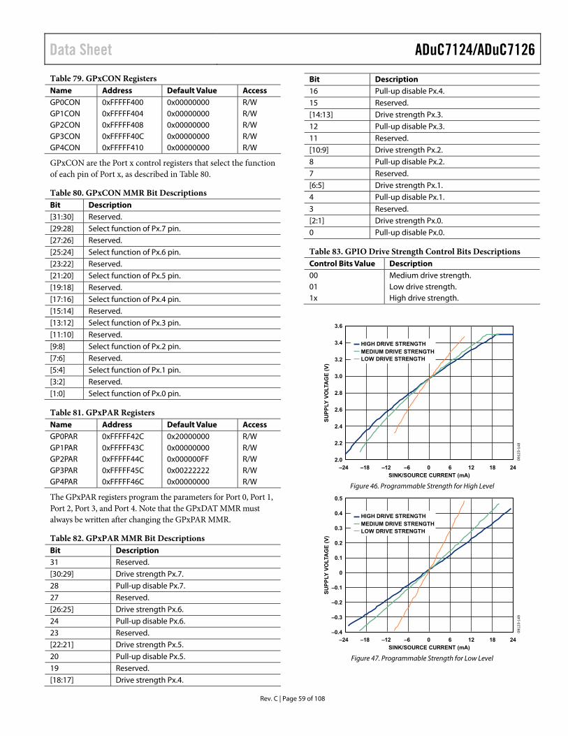
Data Sheet ADuC7124/ADuC7126
Rev. C | Page 59 of 108
Table 79. GPxCON Registers Name Address Default Value Access GP0CON 0xFFFFF400 0x00000000 R/W GP1CON 0xFFFFF404 0x00000000 R/W GP2CON 0xFFFFF408 0x00000000 R/W GP3CON 0xFFFFF40C 0x00000000 R/W GP4CON 0xFFFFF410 0x00000000 R/W
GPxCON are the Port x control registers that select the function of each pin of Port x, as described in Table 80.
Table 80. GPxCON MMR Bit Descriptions Bit Description [31:30] Reserved. [29:28] Select function of Px.7 pin. [27:26] Reserved. [25:24] Select function of Px.6 pin. [23:22] Reserved. [21:20] Select function of Px.5 pin. [19:18] Reserved. [17:16] Select function of Px.4 pin. [15:14] Reserved. [13:12] Select function of Px.3 pin. [11:10] Reserved. [9:8] Select function of Px.2 pin. [7:6] Reserved. [5:4] Select function of Px.1 pin. [3:2] Reserved. [1:0] Select function of Px.0 pin.
Table 81. GPxPAR Registers Name Address Default Value Access GP0PAR 0xFFFFF42C 0x20000000 R/W GP1PAR 0xFFFFF43C 0x00000000 R/W GP2PAR 0xFFFFF44C 0x000000FF R/W GP3PAR 0xFFFFF45C 0x00222222 R/W GP4PAR 0xFFFFF46C 0x00000000 R/W
The GPxPAR registers program the parameters for Port 0, Port 1, Port 2, Port 3, and Port 4. Note that the GPxDAT MMR must always be written after changing the GPxPAR MMR.
Table 82. GPxPAR MMR Bit Descriptions Bit Description 31 Reserved. [30:29] Drive strength Px.7. 28 Pull-up disable Px.7. 27 Reserved. [26:25] Drive strength Px.6. 24 Pull-up disable Px.6. 23 Reserved. [22:21] Drive strength Px.5. 20 Pull-up disable Px.5. 19 Reserved. [18:17] Drive strength Px.4.
Bit Description 16 Pull-up disable Px.4. 15 Reserved. [14:13] Drive strength Px.3. 12 Pull-up disable Px.3. 11 Reserved. [10:9] Drive strength Px.2. 8 Pull-up disable Px.2. 7 Reserved. [6:5] Drive strength Px.1. 4 Pull-up disable Px.1. 3 Reserved. [2:1] Drive strength Px.0. 0 Pull-up disable Px.0.
Table 83. GPIO Drive Strength Control Bits Descriptions Control Bits Value Description 00 Medium drive strength. 01 Low drive strength. 1x High drive strength.
2.0
2.2
2.4
2.6
2.8
3.0
3.2
3.4
3.6
–24 –18 –12 –6 0 6 12 18 24SINK/SOURCE CURRENT (mA)
SUPP
LY V
OLT
AG
E (V
)
HIGH DRIVE STRENGTHMEDIUM DRIVE STRENGTHLOW DRIVE STRENGTH
0912
3-14
8
Figure 46. Programmable Strength for High Level
–0.4
–0.3
–0.2
–0.1
0.1
0
0.2
0.3
0.4
0.5
–24 –18 –12 –6 0 6 12 18 24SINK/SOURCE CURRENT (mA)
SUPP
LY V
OLT
AG
E (V
)
HIGH DRIVE STRENGTHMEDIUM DRIVE STRENGTHLOW DRIVE STRENGTH
0912
3-14
9
Figure 47. Programmable Strength for Low Level
ADuC7124/ADuC7126 Data Sheet
Rev. C | Page 60 of 108
The drive strength bits can be written only once after reset. Additional writing to related bits has no effect on drive strength. The GPIO drive strength and pull-up disable are not always adjustable for GPIO port. Some control bits cannot be changed. See Table 78 for details.
Table 84. GPxDAT Registers Name Address Default Value Access GP0DAT 0xFFFFF420 0x000000XX R/W GP1DAT 0xFFFFF430 0x000000XX R/W GP2DAT 0xFFFFF440 0x000000XX R/W GP3DAT 0xFFFFF450 0x000000XX R/W GP4DAT 0xFFFFF460 0x000000XX R/W
The GPxDAT are Port x configuration and data registers. They configure the direction of the GPIO pins of Port x, set the output value for the pins configured as output, and store the input value of the pins configured as input.
Table 85. GPxDAT MMR Bit Descriptions Bit Description [31:24] Direction of the data.
Set to 1 by the user to configure the GPIO pin as an output. Cleared to 0 by the user to configure the GPIO pin as an input.
[23:16] Port x data output. [15:8] Reflect the state of Port x pins at reset (read only). [7:0] Port x data input (read only).
Table 86. GPxSET Registers Name Address Default Value Access GP0SET 0xFFFFF424 0x000000XX W GP1SET 0xFFFFF434 0x000000XX W GP2SET 0xFFFFF444 0x000000XX W GP3SET 0xFFFFF454 0x000000XX W GP4SET 0xFFFFF464 0x000000XX W
The GPxSET are data set Port x registers.
Table 87. GPxSET MMR Bit Descriptions Bit Description [31:24] Reserved. [23:16] Data Port x set bit.
Set to 1 by the user to set a bit on Port x; also sets the corresponding bit in the GPxDAT MMR. Cleared to 0 by the user; does not affect the data output.
[15:0] Reserved.
Table 88. GPxCLR Registers Name Address Default Value Access GP0CLR 0xFFFFF428 0x000000XX W GP1CLR 0xFFFFF438 0x000000XX W GP2CLR 0xFFFFF448 0x000000XX W GP3CLR 0xFFFFF458 0x000000XX W GP4CLR 0xFFFFF468 0x000000XX W
The GPxCLR are data clear Port x registers.
Table 89. GPxCLR MMR Bit Descriptions Bit Description [31:24] Reserved. [23:16] Data Port x clear bit.
Set to 1 by the user to clear a bit on Port x; also clears the corresponding bit in the GPxDAT MMR. Cleared to 0 by the user; does not affect the data out.
[15:0] Reserved.
SERIAL PORT MUX The serial port mux multiplexes the serial port peripherals (an SPI, UART, and two I2Cs) and the programmable logic array (PLA) to a set of 10 GPIO pins. Each pin must be configured to one of its specific I/O functions as described in Table 90.
Table 90. SPM Configuration GPIO UART UART/I2C/SPI PLA
SPM (00) (01) (10) (11) SPM0 P1.0 SIN0 I2C0SCL PLAI[0] SPM1 P1.1 SOUT0 I2C0SDA PLAI[1] SPM2 P1.2 RTS I2C1SCL PLAI[2] SPM3 P1.3 CTS I2C1SDA PLAI[3] SPM4 P1.4 RI SCLK PLAI[4] SPM5 P1.5 DCD MISO PLAI[5] SPM6 P1.6 DSR MOSI PLAI[6] SPM7 P1.7 DTR CS
PLAO[0]
SPM8 P0.7 ECLK/XCLK SIN0 PLAO[4] SPM9 P2.0 CONVSTART SOUT0 PLAO[5]
SPM10 P4.0 SIN1 AD8 PLAO[8] SPM11 P4.1 SOUT1 AD9 PLAO[9] SPM12 P2.3 N/A AE SIN1 SPM13 P2.4 PWM0 MSO SOUT1
Table 90 also details the mode for each of the SPMMUX pins. This configuration has to be done via the GP0CON, GP1CON, and GP2CON MMRs. By default, these 10 pins are configured as GPIOs.
UART SERIAL INTERFACE The UART peripheral is a full-duplex, universal, asynchronous receiver/transmitter. The UART performs serial-to-parallel conver-sions on data characters received from a peripheral device and parallel-to-serial conversions on data characters received from the CPU. The ADuC7124/ADuC7126 has been equipped with two industry standard 16,450 type UARTs (UART0 and UART1). Each UART features a fractional divider that facilitates high accu-racy baud rate generation and is equipped with a 16-byte FIFO for the transmitter and a 16-byte FIFO for the receiver. Both UARTs can be configured as FIFO mode and non-FIFO mode.
The serial communication adopts an asynchronous protocol, which supports various word lengths, stop bits, and parity generation options selectable in the configuration register.
Data Sheet ADuC7124/ADuC7126
Rev. C | Page 61 of 108
Baud Rate Generation
There are two ways of generating the UART baud rate, using normal 450 UART baud rate generation and using the fractional divider.
Normal 450 UART Baud Rate Generation
The baud rate is a divided version of the core clock using the value in the COMxDIV0 and COMxDIV1 MMRs (16-bit value, DL).
DLRateBaud CD ×××
=2162
MHz78.41
Table 91 gives some common baud rate values.
Table 91. Baud Rate Using the Normal Baud Rate Generator Baud Rate CD DL Actual Baud Rate % Error 9600 0 0x88 9600 0 19,200 0 0x44 19,200 0 115,200 0 0x0B 118,691 3 9600 3 0x11 9600 0 19,200 3 0x08 20,400 6.25 115,200 3 0x01 163,200 41.67
The Fractional Divider
The fractional divider, combined with the normal baud rate generator, produces a wider range of more accurate baud rates.
0912
3-03
2÷ 16DL UART
FBENCORECLOCK ÷ 2
÷ (M + N ÷ 2048)
Figure 48. Baud Rate Generation Options
Calculation of the baud rate using fractional divider is as follows:
⎟⎠⎞
⎜⎝⎛ +××××
=
20482162
MHz78.41NMDL
RateBaudCD
2162MHz78.41
2048 ××××=+
DLRateBaudNM CD
For example, generation of 19,200 baud with CD bits = 3 (Table 91 gives DL = 0x08) is
28162200,19MHz78.41
2048 3 ××××=+
NM
06.12048
=+NM
where: M = 1. N = 0.06 × 2048 = 128.
⎟⎠⎞
⎜⎝⎛××××
=
204812828162
MHz78.41
3RateBaud
where: Baud Rate = 19,200 bps.
Error is 0%, compared to 6.25% with the normal baud rate generator.
UART Register Definitions
COM0TX Register
Name: COM0TX
Address: 0xFFFF0700
Default Value: 0x00
Access: Read/write
COM0TX is an 8-bit transmit register for UART0.
COM1TX Register
Name: COM1TX
Address: 0xFFFF0740
Default Value: 0x00
Access: Read/write
COM1TX is an 8-bit transmit register for UART1.
COM0RX Register
Name: COM0RX
Address: 0xFFFF0700
Default Value: 0x00
Access: Read only
COM0RX is an 8-bit receive register for UART0.
COM1RX Register
Name: COM1RX
Address: 0xFFFF0740
Default Value: 0x00
Access: Read only
COM1RX is an 8-bit receive register for UART1.
COM0DIV0 Register
Name: COM0DIV0
Address: 0xFFFF0700
Default Value: 0x00
Access: Read/write
COM0DIV0 is a low byte divisor latch for UART0. COM0TX, COM0RX, and COM0DIV0 share the same address location. COM0TX and COM0RX can be accessed when Bit 7 in the COM0CON0 register is cleared. COM0DIV0 can be accessed when Bit 7 of COM0CON0 is set.
ADuC7124/ADuC7126 Data Sheet
Rev. C | Page 62 of 108
COM1DIV0 Register
Name: COM1DIV0
Address: 0xFFFF0740
Default Value: 0x00
Access: Read/write
COM1DIV0 is a low byte divisor latch for UART1. COM1TX, COM1RX, and COM1DIV0 share the same address location. COM1TX and COM1RX can be accessed when Bit 7 in COM1CON0 register is cleared. COM1DIV0 can be accessed when Bit 7 of COM1CON0 is set.
COM0IEN0 Register
Name: COM0IEN0
Address: 0xFFFF0704
Default Value: 0x00
Access: Read/write
COM0IEN0 is the interrupt enable register for UART0.
COM1IEN0 Register
Name: COM1IEN0
Address: 0xFFFF0744
Default Value: 0x00
Access: Read/write
COM1IEN0 is the interrupt enable register for UART1.
Table 92. COMxIEN0 MMR Bit Descriptions Bit Name Description [7:4] Reserved. 3 EDSSI Modem status interrupt enable bit.
Set by the user to enable generation of an interrupt if any of COMXSTA1[3:1] are set. Cleared by the user.
2 ELSI Rx status interrupt enable bit. Set by the user to enable generation of an interrupt if any of COMxSTA0[3:0] are set. Cleared by the user.
1 ETBEI Enable transmit buffer empty interrupt. Set by the user to enable interrupt when the buffer is empty during a transmission. Cleared by the user.
0 ERBFI Enable receive buffer full interrupt. In non-FIFO mode, set by the user to enable an interrupt when buffer is full during a reception. Cleared by the user. In FIFO mode, set by the user to enable an interrupt when trigger level is reached. It also controls the character receive timeout interrupt. Cleared by the user.
COM0DIV1 Register
Name: COM0DIV1
Address: 0xFFFF0704
Default Value: 0x00
Access: Read/write
COM0DIV1 is a divisor latch (high byte) register for UART0.
COM1DIV1 Register
Name: COM1DIV1
Address: 0xFFFF0744
Default Value: 0x00
Access: Read/write
COM1DIV1 is a divisor latch (high byte) register for UART1.
COM0IID0 Register
Name: COM0IID0
Address: 0xFFFF0708
Default Value: 0x01
Access: Read only
COM0IID0 is the interrupt identification register for UART0. It also indicates if the UART is in FIFO mode.
COM1IID0 Register
Name: COM1IID0
Address: 0xFFFF0748
Default Value: 0x01
Access: Read only
COM1IID0 is the interrupt identification register for UART1. It also indicates if the UART is in FIFO mode.

Data Sheet ADuC7124/ADuC7126
Rev. C | Page 63 of 108
Table 93. COMxIID0 MMR Bit Descriptions Bit Name Description [7:6] FIFOMODE FIFO mode flag. 0x0: non-FIFO mode. 0x1: reserved. 0x2: reserved. 0x3: FIFO mode. Set automatically if
FIFOEN is set. [5:4] Reserved [3:1] STATUS[2:0] Interrupt status bits that work only when
NINT is set. [000]: modem status interrupt. Cleared by reading COMxSTA1. Priority 4. [001]: for non-FIFO mode, transmit buffer empty interrupt. For FIFO mode, Tx FIFO is empty. Cleared by writing COMxTX or reading COMxIID0. Priority 3. [010]: non-FIFO mode. Receive buffer data ready interrupt. Cleared automatically by reading COMxRX. For FIFO mode, set trigger level reached. Cleared automatically when FIFO drops below the trigger level. Priority 2. [011]: receive line status error interrupt. Cleared by reading COMxSTA0. Priority 1. [110]: Rx FIFO timeout interrupt (FIFO mode only). Set automatically if there is at least one byte in the Rx FIFO, and there is no access to the Rx FIFO in the next four-frames accessing cycle. Cleared by reading COMxRX, setting RXRST, or when a new byte arrives in the Rx FIFO1. Priority 2. [Other state]: reserved.
0 NINT Set to disable interrupt flags by STATUS[2:0]. Clear to enable interrupt.
1 A frame time is the time allotted for one start bit, n data bits, one parity bit, and one stop bit. Here, n is the word length selected with the WLS bits in COMxCON0. WLS[1:0] = 00: timeout threshold = time for 32 bits = (1 + 5 + 1 + 1) × 4. WLS[1:0] = 01: timeout threshold = time for 36 bits = (1 + 6 + 1 + 1) × 4. WLS[1:0] = 10: timeout threshold = time for 40 bits = (1 + 7 + 1 + 1) × 4. WLS[1:0] = 11: timeout threshold = time for 44 bits = (1 + 8 + 1 + 1) × 4.
COM0FCR Register
Name: COM0FCR
Address: 0xFFFF0708
Default Value: 0x00
Access: Read/write
The FIFO control register (FCR) is a write-only register at the same address as the interrupt identification register (IIR), which is a read-only register.
COM1FCR Register
Name: COM1FCR
Address: 0xFFFF0748
Default Value: 0x00
Access: Read/write
The FIFO control register (FCR) is a write-only register at the same address as the interrupt identification register (IIR), which is a read-only register.
Table 94. COMxFCR MMR Bit Descriptions Bit Name Description [7:5] RXFIFOTL Receiver FIFO trigger level. RXFIFOTL sets the
trigger level for the receiver FIFO. When the trigger level is reached, a receiver data-ready interrupt is generated (if the interrupt request is enabled). When the FIFO drops below the trigger level, the interrupt is cleared.
0x0: one byte. 0x1: two bytes. 0x2: four bytes. 0x3: six bytes. 0x4: eight bytes. 0x5: 10 bytes. 0x6: 12 bytes. 0x7: 14 bytes. [4:3] Reserved 2 TXRST Tx FIFO reset. Writing a 1 flushes the Tx FIFO.
Does not affect shift register. Note that TXRST should be cleared manually to make Tx FIFO work after flushing.
1 RXRST Rx FIFO reset. Writing a 1 flushes the Rx FIFO. Does not affect shift register. Note that RXRST should be cleared manually to make the Rx FIFO work after flushing.
0 FIFOEN Transmitter and receiver FIFOs mode enable. FIFOEN must be set before other FCR bits are written to. Set for FIFO mode. The transmitter and receiver FIFOs are enabled. Cleared for non-FIFO mode; the transmitter and receiver FIFOs are disabled, and the FIFO pointers are cleared.
COM0CON0 Register
Name: COM0CON0
Address: 0xFFFF070C
Default Value: 0x00
Access: Read/write
COM0CON0 is the line control register for UART0.
ADuC7124/ADuC7126 Data Sheet
Rev. C | Page 64 of 108
COM1CON0 Register
Name: COM1CON0
Address: 0xFFFF074C
Default Value: 0x00
Access: Read/write
COM1CON0 is the line control register for UART1.
Table 95. COMxCON0 MMR Bit Descriptions Bit Name Description 7 DLAB Divisor latch access.
Set by the user to enable access to the COMxDIV0 and COMxDIV1 registers. Cleared by the user to disable access to COMxDIV0 and COMxDIV1 and enable access to COMxRX and COMxTX.
6 BRK Set break. Set by the user to force SOUTx to 0. Cleared to operate in normal mode.
5 SP Stick parity. Set by the user to force parity to defined values: 1 if EPS = 1 and PEN = 1, 0 if EPS = 0 and PEN = 1.
4 EPS Even parity select bit. Set for even parity. Cleared for odd parity.
3 PEN Parity enable bit. Set by the user to transmit and check the parity bit. Cleared by the user for no parity transmission or checking.
2 Stop Stop bit. Set by the user to transmit 1½ stop bits if the word length is five bits or two stop bits if the word length is six bits, seven bits, or eight bits. The receiver checks the first stop bit only, regardless of the number of stop bits selected. Cleared by the user to generate one stop bit in the transmitted data.
[1:0] WLS Word length select: 00 = five bits, 01 = six bits, 10 = seven bits, 11 = eight bits.
COM0CON1 Register
Name: COM0CON1
Address: 0xFFFF0710
Default Value: 0x00
Access: Read/write
COM0CON1 is the modem control register for UART0.
COM1CON1 Register
Name: COM1CON1
Address: 0xFFFF0750
Default Value: 0x00
Access: Read/write
COM1CON1 is the modem control register for UART1.
Table 96. COMxCON1 MMR Bit Descriptions Bit Name Description [7:5] Reserved. 4 LOOPBACK Loop back.
Set by the user to enable loopback mode. In loopback mode, SOUTx is forced high. The modem signals are also directly con-nected to the status inputs (RTS to CTS and DTR to DSR). Cleared by the user to be in normal mode.
3 PEN Parity enable bit. Set by the user to transmit and check the parity bit. Cleared by the user for no parity transmission or checking.
2 Stop Stop bit. Set by the user to transmit 1½ stop bits if the word length is five bits or two stop bits if the word length is six bits, seven bits, or eight bits. The receiver checks the first stop bit only, regardless of the number of stop bits selected. Cleared by the user to generate one stop bit in the transmitted data.
1 RTS Request to send. Set by the user to force the RTS output to 0. Cleared by the user to force the RTS output to 1.
0 DTR Data terminal ready. Set by the user to force the DTR output to 0. Cleared by the user to force the DTR output to 1.
COM0STA0 Register
Name: COM0STA0
Address: 0xFFFF0714
Default Value: 0xE0
Access: Read only
COM0STA0 is the line status register for UART0.

Data Sheet ADuC7124/ADuC7126
Rev. C | Page 65 of 108
COM1STA0 Register
Name: COM1STA0
Address: 0xFFFF0754
Default Value: 0xE0
Access: Read only
COM1STA0 is the line status register for UART1.
Table 97. COMxSTA0 MMR Bit Descriptions Bit Name Description 11 RX_error Set automatically if PE, FE, or BI is set.
Cleared automatically when PE, FE, and BI are cleared .
10 RX_timeout Only for FIFO mode. Set automatically if there is at least one byte in the Rx FIFO and there is no access to the Rx FIFO in the next 4-byte accessing cycle.
9 RX_triggered Only for FIFO mode. Set automatically if the Rx FIFO number exceeds the trigger level, which is configured by the FIFO control register COMxFCR[7:5]. Cleared automatically when the Rx FIFO number is equal to or less than the trigger level.
8 TX_full Only for FIFO mode. Set automatically if Tx FIFO is full. Cleared automatically when Tx FIFO is not full.
7 TX_half_empty Only for FIFO mode. Set automatically if the Tx FIFO is half empty (number of bytes in Tx FIFO ≤ 8). Cleared automati-cally when the Tx FIFO received bytes is more than eight bytes.
6 TEMT COMxTX empty status bit. For non-FIFO mode, both THR and TSR are empty. For FIFO mode, both Tx FIFO and TSR are empty.
5 THRE COMxTX and transmitter shift register empty. For non-FIFO mode, transmitter hold register (THR) empty or the content of THR has been transferred to the transmitter shift register (TSR). For FIFO mode, Tx FIFO is empty, or the last character in the FIFO has been transferred to the transmitter shift register (TSR).
4 BI Break error. Set when SINx is held low for more than the maximum word length. Cleared automatically.
3 FE Framing error. Set when an invalid stop bit occurs. Cleared automatically.
2 PE Parity error. Set when a parity error occurs. Cleared automatically.
Bit Name Description 1 OE Overrun error.
For non-FIFO mode, set automatically if data is overwritten before being read. Cleared automatically. For FIFO mode, set automatically if an overrun error has been detected. An overrun error occurs only after the FIFO is full and the next character has been completely received in the shift register. The new character overwrites the character in the shift register, but it is not transferred to the FIFO.
0 DR Data ready. For non-FIFO mode, set automatically when COMxRX is full. Cleared by reading COMxRX. For FIFO mode, set automatically when there is at least one unread byte in the COMxRX.
COM0STA1 Register
Name: COM0STA1
Address: 0xFFFF0718
Default Value: 0x00
Access: Read only
COM0STA1 is a modem status register.
COM1STA1 Register
Name: COM1STA1
Address: 0xFFFF0758
Default Value: 0x00
Access: Read only
COM1STA1 is a modem status register.
Table 98. COMxSTA1 MMR Bit Descriptions Bit Name Description 7 DCD Data carrier detect. 6 RI Ring indicator. 5 DSR Data set ready. 4 CTS Clear to send. 3 DDCD Delta DCD. Set automatically if DCD changed
state since last COMxSTA1 read. Cleared automatically by reading COMxSTA1.
2 TERI Trailing edge RI. Set if RI changed from 0 to 1 since COMxSTA1 last read. Cleared automatically by reading COMxSTA1.
1 DDSR Delta DSR. Set automatically if DSR changed state since COMxSTA1 last read. Cleared automatically by reading COMxSTA1.
0 DCTS Delta CTS. Set automatically if CTS changed state since COMxSTA1 last read. Cleared automatically by reading COMxSTA1.
ADuC7124/ADuC7126 Data Sheet
Rev. C | Page 66 of 108
COM0DIV2 Register
Name:
MOSI (Master Out, Slave In) Pin
COM0DIV2
Address: 0xFFFF072C
The MOSI pin is configured as an output line in master mode and an input line in slave mode. The MOSI line on the master (data out) should be connected to the MOSI line in the slave device (data in). The data is transferred as byte wide (8-bit) serial data, MSB first.
Default Value: 0x0000
Access: Read/write SCLK (Serial Clock I/O) Pin
COM0DIV2 is a 16-bit fractional baud divide register for UART0.
COM1DIV2 Register
Name: COM1DIV2
The master serial clock (SCLK) synchronizes the data being transmitted and received through the MOSI SCLK period. Therefore, a byte is transmitted/received after eight SCLK periods. The SCLK pin is configured as an output in master mode and as an input in slave mode.
Address: 0xFFFF076C In master mode, polarity and phase of the clock are controlled by the SPICON register, and the bit rate is defined in the SPIDIV register as follows: Default Value: 0x0000
Access: Read/write
)1(2 SPIDIVf
f UCLKCLOCKSERIAL +×
= COM1DIV2 is a 16-bit fractional baud divide register for UART1.
The maximum speed of the SPI clock is independent of the clock divider bits. Table 99. COMxDIV2 MMR Bit Descriptions
Bit Name Description In slave mode, the SPICON register must be configured with the phase and polarity of the expected input clock. The slave accepts data from an external master up to 10 Mbps.
15 FBEN Fractional baud rate generator enable bit. Set by the user to enable the fractional baud rate generator. Cleared by the user to generate the baud rate using the standard 450 UART baud rate generator.
In both master and slave modes, data is transmitted on one edge of the SCLK signal and sampled on the other. Therefore, it is important that the polarity and phase be configured the same for the master and slave devices. [14:13] Reserved.
[12:11] FBM[1:0] M if FBM = 0, M = 4 (see The Fractional Divider section). CS (SPI Chip Select Input) Pin
[10:0] FBN[10:0] N (see The Fractional Divider section). In SPI slave mode, a transfer is initiated by the assertion of CS, which is an active low input signal. The SPI port then transmits and receives 8-bit data until the transfer is concluded by deasser-tion of CS. In slave mode, CS is always an input.
SERIAL PERIPHERAL INTERFACE The ADuC7124/ADuC7126 integrate a complete hardware serial peripheral interface (SPI) on chip. SPI is an industry standard, synchronous serial interface that allows eight bits of data to be synchronously transmitted and simultaneously received, that is, full duplex up to a maximum bit rate of 20 Mbps.
In SPI master mode, the CS is an active low output signal. It asserts itself automatically at the beginning of a transfer and deasserts itself upon completion.
Configuring External Pins for SPI functionality
The SPI port can be configured for master or slave operation and typically consists of four pins: MISO, MOSI, SCLK, and CS.
The SPI pins of the ADuC7124/ADuC7126 device are P1.4 to P1.7.
P1.7 is the slave chip select pin. In slave mode, this pin is an input and must be driven low by the master. In master mode, this pin is an output and goes low at the beginning of a transfer and high at the end of a transfer.
MISO (Master In, Slave Out) Pin
The MISO pin is configured as an input line in master mode and an output line in slave mode. The MISO line on the master (data in) should be connected to the MISO line in the slave device (data out). The data is transferred as byte wide (8-bit) serial data, MSB first.
P1.4 is the SCLK pin.
P1.5 is the master in, slave out (MISO) pin.
P1.6 is the master out, slave in (MOSI) pin.
To configure P1.4 to P1.7 for SPI mode, see the General-Purpose Input/Output section.

Data Sheet ADuC7124/ADuC7126
Rev. C | Page 67 of 108
SPI Registers
The following MMR registers control the SPI interface: SPISTA, SPIRX, SPITX, SPIDIV, and SPICON.
SPI Status Register
Name: SPISTA
Address: 0xFFFF0A00
Default Value: 0x0000
Access: Read only
Function: This 32-bit MMR contains the status of the SPI interface in both master and slave modes.
Table 100. SPISTA MMR Bit Descriptions Bit Name Description [15:12] Reserved. 11 SPIREX SPI Rx FIFO excess bytes present. This bit is set when there are more bytes in the Rx FIFO than indicated in the
SPIMDE bits in SPICON This bit is cleared when the number of bytes in the FIFO is equal to or less than the number in SPIMDE. [10:8] SPIRXFSTA[2:0] SPI Rx FIFO status bits. [000] = Rx FIFO is empty. [001] = one valid byte in the FIFO. [010] = two valid bytes in the FIFO. [011] = three valid bytes in the FIFO. [100] = four valid bytes in the FIFO. 7 SPIFOF SPI Rx FIFO overflow status bit. Set when the Rx FIFO was already full when new data was loaded to the FIFO. This bit generates an interrupt
except when SPIRFLH is set in SPICON. Cleared when the SPISTA register is read. 6 SPIRXIRQ SPI Rx IRQ status bit. Set when a receive interrupt occurs. This bit is set when SPITMDE in SPICON is cleared and the required
number of bytes has been received. Cleared when the SPISTA register is read.
SPITXIRQ SPI Tx IRQ status bit. Set when a transmit interrupt occurs. This bit is set when SPITMDE in SPICON is set and the required number
of bytes has been transmitted.
5
Cleared when the SPISTA register is read. 4 SPITXUF SPI Tx FIFO underflow. This bit is set when a transmit is initiated without any valid data in the Tx FIFO. This bit generates an interrupt
except when SPITFLH is set in SPICON. Cleared when the SPISTA register is read. [3:1] SPITXFSTA[2:0] SPI Tx FIFO status bits. [000] = Tx FIFO is empty. [001] = one valid byte in the FIFO. [010] = two valid bytes in the FIFO. [011] = three valid bytes in the FIFO. [100] = four valid bytes in the FIFO. 0 SPIISTA SPI interrupt status bit. Set to 1 when an SPI-based interrupt occurs. Cleared after reading SPISTA.

ADuC7124/ADuC7126 Data Sheet
Rev. C | Page 68 of 108
SPIRX Register
Name: SPIRX
Address: 0xFFFF0A04
Default Value: 0x00
Access: Read only
Function: This 8-bit MMR is the SPI receive register.
SPITX Register
Name: SPITX
Address: 0xFFFF0A08
Default Value: 0x00
Access: Write only
Function: This 8-bit MMR is the SPI transmit register.
SPIDIV Register
Name: SPIDIV
Address: 0xFFFF0A0C
Default Value: 0x00
Access: Read/write
Function: This 8-bit MMR is the SPI baud rate selection register.
SPICON Register
Name: SPICON
Address: 0xFFFF0A10
Default Value: 0x0000
Access: Read/write
Function: This 16-bit MMR configures the SPI peripheral in both master and slave modes.
Table 101. SPICON MMR Bit Descriptions Bit Name Description [15:14] SPIMDE SPI IRQ mode bits. These bits configure when the Tx/Rx interrupts occur in a transfer. [00] = Tx interrupt occurs when one byte has been transferred. Rx interrupt occurs when one or more bytes have
been received into the FIFO. [01] = Tx interrupt occurs when two bytes have been transferred. Rx interrupt occurs when two or more bytes have been received into the FIFO. [10] = Tx interrupt occurs when three bytes have been transferred. Rx interrupt occurs when three or more bytes have been received into the FIFO. [11] = Tx interrupt occurs when four bytes have been transferred. Rx interrupt occurs when the Rx FIFO is full or four bytes are present.
13 SPITFLH SPI Tx FIFO flush enable bit. Set this bit to flush the Tx FIFO. This bit does not clear itself and should be toggled if a single flush is required.
If this bit is left high, then either the last transmitted value or 0x00 is transmitted, depending on the SPIZEN bit. Any writes to the Tx FIFO are ignored while this bit is set.
Clear this bit to disable Tx FIFO flushing. 12 SPIRFLH SPI Rx FIFO flush enable bit. Set this bit to flush the Rx FIFO. This bit does not clear itself and should be toggled if a single flush is required.
If this bit is set incoming, data is ignored and no interrupts are generated. If set and SPITMDE = 0, a read of the Rx FIFO initiates a transfer.
Clear this bit to disable Rx FIFO flushing. Continuous transfer enable. Set by the user to enable continuous transfer. In master mode, the transfer continues until no valid data is available in the SPITX register. CS is asserted and remains asserted for the duration of each 8-bit serial transfer until SPITX is empty.
11 SPICONT
Cleared by the user to disable continuous transfer. Each transfer consists of a single 8-bit serial transfer. If valid data exists in the SPITX register, then a new transfer is initiated after a stall period of one serial clock cycle.
10 SPILP Loopback enable bit. Set by the user to connect MISO to MOSI and test software. Cleared by the user to be in normal mode.
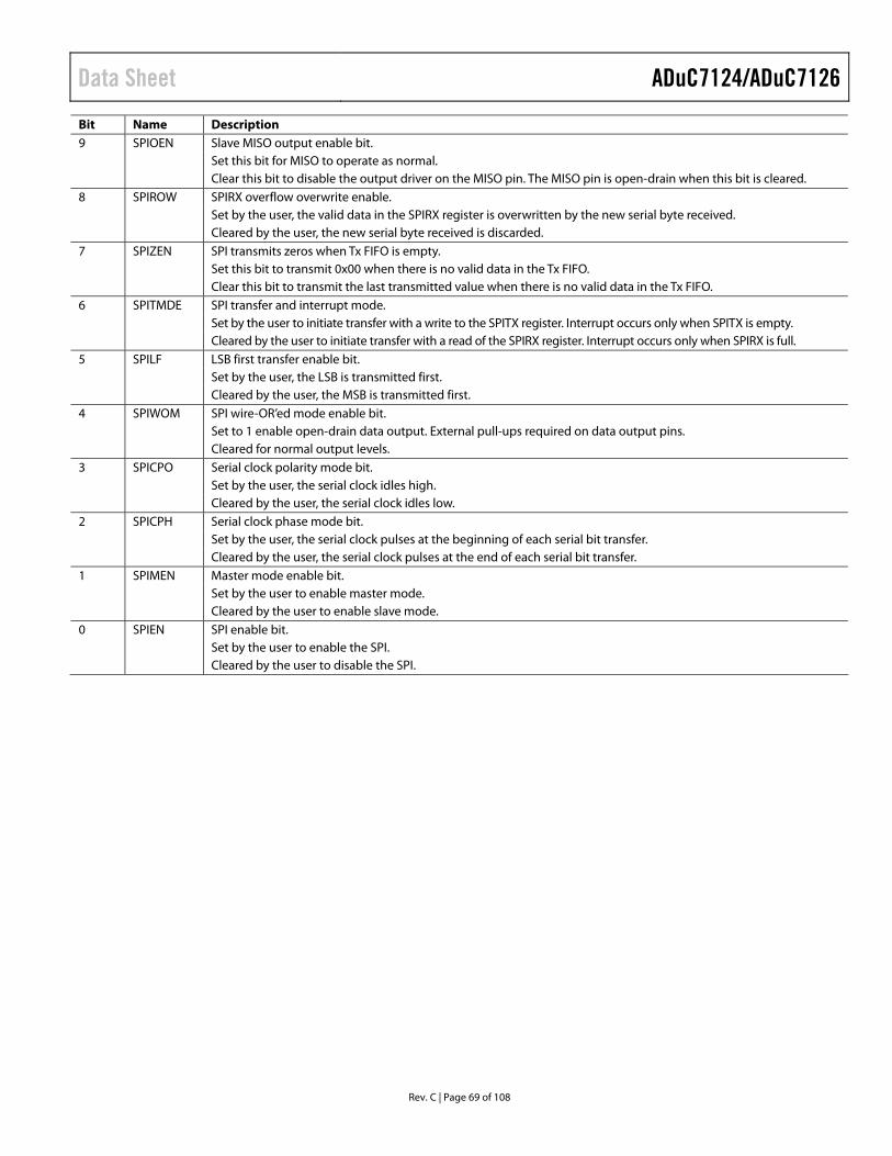
Data Sheet ADuC7124/ADuC7126
Rev. C | Page 69 of 108
Bit Name Description 9 SPIOEN Slave MISO output enable bit. Set this bit for MISO to operate as normal. Clear this bit to disable the output driver on the MISO pin. The MISO pin is open-drain when this bit is cleared. 8 SPIROW SPIRX overflow overwrite enable. Set by the user, the valid data in the SPIRX register is overwritten by the new serial byte received. Cleared by the user, the new serial byte received is discarded. 7 SPIZEN SPI transmits zeros when Tx FIFO is empty. Set this bit to transmit 0x00 when there is no valid data in the Tx FIFO. Clear this bit to transmit the last transmitted value when there is no valid data in the Tx FIFO. 6 SPITMDE SPI transfer and interrupt mode. Set by the user to initiate transfer with a write to the SPITX register. Interrupt occurs only when SPITX is empty. Cleared by the user to initiate transfer with a read of the SPIRX register. Interrupt occurs only when SPIRX is full. 5 SPILF LSB first transfer enable bit. Set by the user, the LSB is transmitted first. Cleared by the user, the MSB is transmitted first. 4 SPIWOM SPI wire-OR’ed mode enable bit. Set to 1 enable open-drain data output. External pull-ups required on data output pins. Cleared for normal output levels.
Serial clock polarity mode bit. Set by the user, the serial clock idles high.
3 SPICPO
Cleared by the user, the serial clock idles low. 2 SPICPH Serial clock phase mode bit. Set by the user, the serial clock pulses at the beginning of each serial bit transfer. Cleared by the user, the serial clock pulses at the end of each serial bit transfer. 1 SPIMEN Master mode enable bit. Set by the user to enable master mode. Cleared by the user to enable slave mode. 0 SPIEN SPI enable bit. Set by the user to enable the SPI. Cleared by the user to disable the SPI.

ADuC7124/ADuC7126 Data Sheet
Rev. C | Page 70 of 108
I2C The ADuC7124/ADuC7126 incorporate two I2C peripherals that can be configured as a fully I2C-compatible I2C bus master device or as a fully I2C bus compatible slave device. Both I2C channels are identical. Therefore, the following descriptions apply to both channels.
The two pins used for data transfer, SDA and SCL, are configured in a wire-AND’ed format that allows arbitration in a multimaster system. These pins require external pull-up resistors. Typical pull-up values are between 4.7 kΩ and 10 kΩ.
The I2C bus peripheral address in the I2C bus system is programmed by the user. This ID can be modified any time a transfer is not in progress. The user can configure the interface to respond to four slave addresses.
The transfer sequence of an I2C system consists of a master device initiating a transfer by generating a start condition while the bus is idle. The master transmits the slave device address and the direction of the data transfer (read or/write) during the initial address transfer. If the master does not lose arbitration and the slave acknowledges, the data transfer is initiated. This continues until the master issues a stop condition and the bus becomes idle.
The I2C peripheral can only be configured as a master or slave at any given time. The same I2C channel cannot simultaneously support master and slave modes.
The I2C interface on the ADuC7124/ADuC7126 includes the following features:
• Support for repeated start conditions. In master mode, the ADuC7124/ADuC7126 can be programmed to generate a repeated start. In slave mode, the ADuC7124/ADuC7126 recognizes repeated start conditions.
• In master and slave mode, the part recognizes both 7-bit and 10-bit bus addresses.
• In I2C master mode, the ADuC7124/ADuC7126 supports continuous reads from a single slave up to 512 bytes in a single transfer sequence.
• Clock stretching is supported in both master and slave modes. • In slave mode, the ADuC7124/ADuC7126 can be pro-
grammed to return a NACK. This allows the validiation of checksum bytes at the end of I2C transfers.
• Bus arbitration in master mode is supported. • Internal and external loopback modes are supported for
I2C hardware testing in loopback mode. • The transmit and receive circuits in both master and slave
mode contain 2-byte FIFOs. Status bits are available to the user to control these FIFOs.
Configuring External Pins for I2C Functionality
The I2C pins of the ADuC7124/ADuC7126 device are P1.0 and P1.1 for I2C0 and P1.2 and P1.3 for I2C1.
P1.0 and P1.2 are the I2C clock signals, and P1.1 and P1.3 are the I2C data signals. For instance, to configure I2C0 pins (SCL0, SDA0), Bit 0 and Bit 4 of the GP1CON register must be set to 1 to enable I2C mode. On the other hand, to configure I2C1 pins (SCL1, SDA1), Bit 8 and Bit 12 of the GP1CON register must be set to 1 to enable I2C mode, as shown in the General-Purpose Input/Output section.
Serial Clock Generation
The I2C master in the system generates the serial clock for a transfer. The master channel can be configured to operate in fast mode (400 kHz) or standard mode (100 kHz).
The bit rate is defined in the I2CxDIV MMR as follows:
) (2 )2( DIVLDIVH +++= UCLK
CLOCKSERIALf
f
where: fUCLK is the clock before the clock divider. DIVH is the high period of the clock. DIVL is the low period of the clock.
Therefore, for 100 kHz operation,
DIVH = DIVL = 0xCF
and for 400 kHz
DIVH = 0x28, DIVL = 0x3C
The I2CxDIV register corresponds to DIVH:DIVL.
I2C Bus Addresses
Slave Mode
In slave mode, the I2CxID0, I2CxID1, I2CxID2, and I2CxID3 registers contain the device IDs. The device compares the four I2CxIDx registers to the address byte received from the bus master. To be correctly addressed, the seven MSBs of either ID register must be identical to the seven MSBs of the first received address byte. The LSB of the ID registers (the transfer direction bit) is ignored in the process of address recognition.
The ADuC7124/ADuC7126 also support 10-bit addressing mode. When Bit 1 of I2CxSCON (ADR10EN bit) is set to 1, one 10-bit address is supported in slave mode and is stored in the I2CxID0 and I2CxID1 registers. The 10-bit address is derived as follows:
I2CxID0[0] is the read/write bit and is not part of the I2C address.
I2CxID0[7:1] = Address Bits[6:0].
I2CxID1[2:0] = Address Bits[9:7].
I2CxID1[7:3] must be set to 11110b.

Data Sheet ADuC7124/ADuC7126
Rev. C | Page 71 of 108
Master Mode
In master mode, the I2CxADR0 register is programmed with the I2C address of the device.
In 7-bit address mode, I2CxADR0[7:1] are set to the device address. I2CxADR0[0] is the read/write bit.
In 10-bit address mode, the 10-bit address is created as follows:
I2CxADR0[7:3] must be set to 11110b.
I2CxADR0[2:1] = Address Bits[9:8].
I2CxADR1[7:0] = Address Bits[7:0].
I2CxADR0[0] is the read/write bit.
I2C Registers
The I2C peripheral interfaces consists of a number of MMRs. These are described in the I2C Master Registers section.
I2C Master Registers
I2C Master Control Register
Name: I2C0MCON, I2C1MCON
Address: 0xFFFF0800, 0xFFFF0900
Default Value:
0x0000, 0x0000
Access: Read/write
Function: This 16-bit MMR configures the I2C peripheral in master mode.
Table 102. I2CxMCON MMR Bit Descriptions Bit Name Description [15:9] Reserved. These bits are reserved and should not be written to. 8 I2CMCENI I2C transmission complete interrupt enable bit. Set this bit to enable an interrupt on detecting a stop condition on the I2C bus. Clear this bit to clear the interrupt source. 7 I2CNACKENI I2C no acknowledge (NACK) received interrupt enable bit. Set this bit to enable interrupts when the I2C master receives a NACK. Clear this bit to clear the interrupt source. 6 I2CALENI I2C arbitration lost interrupt enable bit. Set this bit to enable interrupts when the I2C master is unable to gain control of the I2C bus. Clear this bit to clear the interrupt source. 5 I2CMTENI I2C transmit interrupt enable bit. Set this bit to enable interrupts when the I2C master has transmitted a byte. Clear this bit to clear the interrupt source. 4 I2CMRENI I2C receive interrupt enable bit. Set this bit to enable interrupts when the I2C master receives data. Cleared by user to disable interrupts when the I2C master is receiving data.
I2CMSEN I2C master SCL stretch enable bit. Set this bit to 1 to enable clock stretching. When SCL is low, setting this bit forces the device to hold SCL low until
I2CMSEN is cleared. If SCL is high, setting this bit forces the device to hold SCL low after the next falling edge.
3
Clear this bit to disable clock stretching. 2 I2CILEN I2C internal loopback enable. Set this bit to enable loopback test mode. In this mode, the SCL and SDA signals are connected internally to their
respective input signals. Cleared by the user to disable loopback mode. 1 I2CBD I2C master backoff disable bit. Set this bit to allow the device to compete for control of the bus even if another device is currently driving a start
condition. Clear this bit to wait until the I2C bus becomes free. 0 I2CMEN I2C master enable bit. Set by the user to enable I2C master mode. Clear this bit to disable I2C master mode.
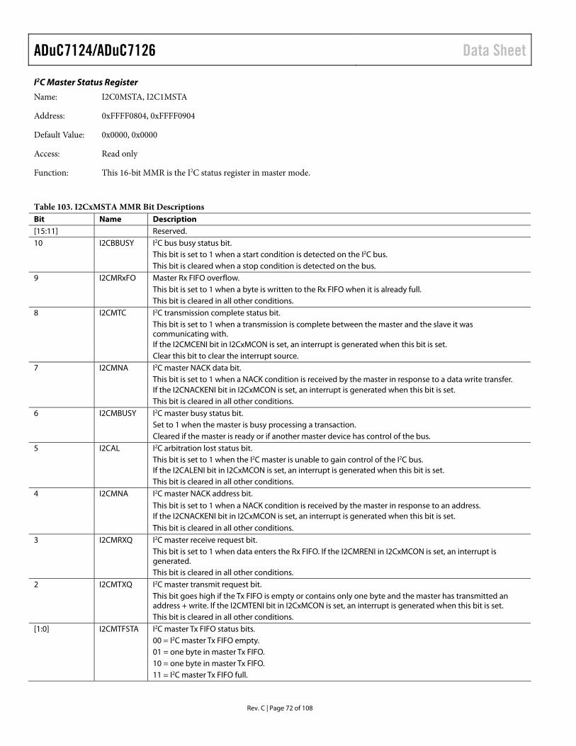
ADuC7124/ADuC7126 Data Sheet
Rev. C | Page 72 of 108
I2C Master Status Register
Name: I2C0MSTA, I2C1MSTA
Address: 0xFFFF0804, 0xFFFF0904
Default Value: 0x0000, 0x0000
Access: Read only
Function: This 16-bit MMR is the I2C status register in master mode.
Table 103. I2CxMSTA MMR Bit Descriptions Bit Name Description [15:11] Reserved. 10 I2CBBUSY I2C bus busy status bit. This bit is set to 1 when a start condition is detected on the I2C bus. This bit is cleared when a stop condition is detected on the bus. 9 I2CMRxFO Master Rx FIFO overflow. This bit is set to 1 when a byte is written to the Rx FIFO when it is already full. This bit is cleared in all other conditions. 8 I2CMTC I2C transmission complete status bit. This bit is set to 1 when a transmission is complete between the master and the slave it was
communicating with. If the I2CMCENI bit in I2CxMCON is set, an interrupt is generated when this bit is set.
Clear this bit to clear the interrupt source. 7 I2CMNA I2C master NACK data bit. This bit is set to 1 when a NACK condition is received by the master in response to a data write transfer.
If the I2CNACKENI bit in I2CxMCON is set, an interrupt is generated when this bit is set. This bit is cleared in all other conditions. 6 I2CMBUSY I2C master busy status bit. Set to 1 when the master is busy processing a transaction. Cleared if the master is ready or if another master device has control of the bus. 5 I2CAL I2C arbitration lost status bit. This bit is set to 1 when the I2C master is unable to gain control of the I2C bus.
If the I2CALENI bit in I2CxMCON is set, an interrupt is generated when this bit is set. This bit is cleared in all other conditions.
I2CMNA I2C master NACK address bit. This bit is set to 1 when a NACK condition is received by the master in response to an address.
If the I2CNACKENI bit in I2CxMCON is set, an interrupt is generated when this bit is set.
4
This bit is cleared in all other conditions. 3 I2CMRXQ I2C master receive request bit. This bit is set to 1 when data enters the Rx FIFO. If the I2CMRENI in I2CxMCON is set, an interrupt is
generated. This bit is cleared in all other conditions. 2 I2CMTXQ I2C master transmit request bit. This bit goes high if the Tx FIFO is empty or contains only one byte and the master has transmitted an
address + write. If the I2CMTENI bit in I2CxMCON is set, an interrupt is generated when this bit is set. This bit is cleared in all other conditions. [1:0] I2CMTFSTA I2C master Tx FIFO status bits. 00 = I2C master Tx FIFO empty. 01 = one byte in master Tx FIFO. 10 = one byte in master Tx FIFO. 11 = I2C master Tx FIFO full.

Data Sheet ADuC7124/ADuC7126
Rev. C | Page 73 of 108
I2C Master Receive Register
Name: I2C0MRX, I2C1MRX
Address: 0xFFFF0808, 0xFFFF0908
Default Value: 0x00
Access: Read only
Function: This 8-bit MMR is the I2C master receive register.
I2C Master Transmit Register
Name: I2C0MTX, I2C1MTX
Address: 0xFFFF080C 0xFFFF090C
Default Value: 0x00, 0x00
Access: Read/write
Function: This 8-bit MMR is the I2C master transmit register.
I2C Master Read Count Register
Name: I2C0MCNT0, I2C1MCNT0
Address: 0xFFFF0810, 0xFFFF0910
Default Value: 0x0000, 0x0000
Access: Read/write
Function: This 16-bit MMR holds the required number of bytes when the master begins a read sequence from a slave device.
Table 104. I2CxMCNT0 MMR Bit Descriptions Bit Name Description [15:9] Reserved. 8 I2CRECNT Set this bit if more than 256 bytes are
required from the slave. Clear this bit when reading 256 bytes or
less. [7:0] I2CRCNT These eight bits hold the number of bytes
required during a slave read sequence, minus 1. If only a single byte is required, these bits should be set to 0.
I2C Master Current Read Count Register
Name: I2C0MCNT1, I2C1MCNT1
Address: 0xFFFF0814, 0xFFFF0914
Default Value: 0x00, 0x00
Access: Read only
Function: This 8-bit MMR holds the number of bytes received so far during a read sequence with a slave device.
I2C Address 0 Register
Name: I2C0ADR0, I2C1ADR0
Address: 0xFFFF0818, 0xFFFF0918
Default Value: 0x00
Access: Read/write
Function: This 8-bit MMR holds the 7-bit slave address + the read/write bit when the master begins communicating with a slave.
Table 105. I2CxADR0 MMR in 7-Bit Address Mode Bit Name Description [7:1] I2CADR These bits contain the 7-bit address of the
required slave device. 0 R/W Bit 0 is the read/write bit. When this bit = 1, a read sequence is
requested. When this bit = 0, a write sequence is
requested.
Table 106. I2CxADR0 MMR in 10-Bit Address Mode Bit Name Description [7:3] These bits must be set to [11110b] in 10-bit
address mode. [2:1] I2CMADR These bits contain ADDR[9:8] in 10-bit
addressing mode. 0 R/W Read/write bit. When this bit = 1, a read sequence is
requested. When this bit = 0, a write sequence is
requested.

ADuC7124/ADuC7126 Data Sheet
Rev. C | Page 74 of 108
I2C Address 1 Register
Name: I2C0ADR1, I2C1ADR1
Address: 0xFFFF081C, 0xFFFF091C
Default Value: 0x00
Access: Read/write
Function: This 8-bit MMR is used in 10-bit addressing mode only. This register contains the least significant byte of the address.
Table 107. I2CxADR1 MMR in 10-Bit Address Mode Bit Name Description [7:0] I2CLADR These bits contain ADDR[7:0] in 10-bit
addressing mode.
I2C Master Clock Control Register
Name: I2C0DIV, I2C1DIV
Address: 0xFFFF0824, 0xFFFF0924
Default Value: 0x1F1F
Access: Read/write
Function: This MMR controls the frequency of the I2C clock generated by the master on to the SCL pin. For further details, see the I2C section.
Table 108. I2CxDIV MMR Bit Name Description [15:8] DIVH These bits control the duration of the high
period of SCL. [7:0] DIVL These bits control the duration of the low
period of SCL.
I2C Slave Registers
I2C Slave Control Register
Name: I2C0SCON, I2C1SCON
Address: 0xFFFF0828, 0xFFFF0928
Default Value: 0x0000
Access: Read/write
Function: This 16-bit MMR configures the I2C peripheral in slave mode.
Table 109. I2CxSCON MMR Bit Descriptions Bit Name Description [15:11] Reserved. 10 I2CSTXENI Slave transmit interrupt enable bit. Set this bit to enable an interrupt after a slave transmits a byte. Clear this interrupt source. 9 I2CSRXENI Slave receive interrupt enable bit. Set this bit to enable an interrupt after the slave receives data. Clear this interrupt source. 8 I2CSSENI I2C stop condition detected interrupt enable bit. Set this bit to enable an interrupt on detecting a stop condition on the I2C bus. Clear this interrupt source. 7 I2CNACKEN I2C NACK enable bit. Set this bit to NACK the next byte in the transmission sequence. Clear this bit to let the hardware control the ACK/NACK sequence. 6 I2CSSEN I2C slave SCL stretch enable bit. Set this bit to 1 to enable clock stretching. When SCL is low, setting this bit forces the device to hold SCL low
until I2CSSEN is cleared. If SCL is high, setting this bit forces the device to hold SCL low after the next falling edge.
Clear this bit to disable clock stretching.
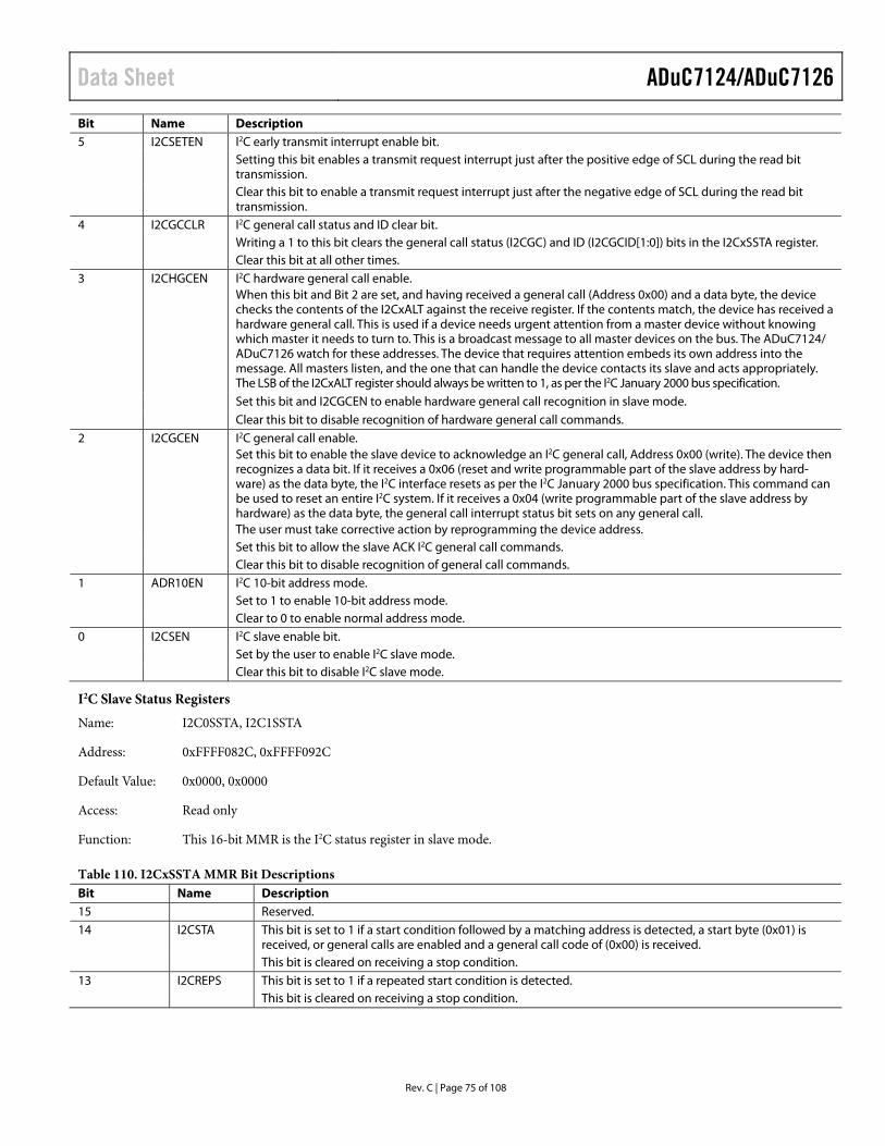
Data Sheet ADuC7124/ADuC7126
Rev. C | Page 75 of 108
Bit Name Description 5 I2CSETEN I2C early transmit interrupt enable bit. Setting this bit enables a transmit request interrupt just after the positive edge of SCL during the read bit
transmission. Clear this bit to enable a transmit request interrupt just after the negative edge of SCL during the read bit
transmission. 4 I2CGCCLR I2C general call status and ID clear bit. Writing a 1 to this bit clears the general call status (I2CGC) and ID (I2CGCID[1:0]) bits in the I2CxSSTA register. Clear this bit at all other times.
I2CHGCEN I2C hardware general call enable. When this bit and Bit 2 are set, and having received a general call (Address 0x00) and a data byte, the device checks the contents of the I2CxALT against the receive register. If the contents match, the device has received a hardware general call. This is used if a device needs urgent attention from a master device without knowing which master it needs to turn to. This is a broadcast message to all master devices on the bus. The ADuC7124/ ADuC7126 watch for these addresses. The device that requires attention embeds its own address into the message. All masters listen, and the one that can handle the device contacts its slave and acts appropriately. The LSB of the I2CxALT register should always be written to 1, as per the I2C January 2000 bus specification.
Set this bit and I2CGCEN to enable hardware general call recognition in slave mode.
3
Clear this bit to disable recognition of hardware general call commands. 2 I2CGCEN I2C general call enable.
Set this bit to enable the slave device to acknowledge an I2C general call, Address 0x00 (write). The device then recognizes a data bit. If it receives a 0x06 (reset and write programmable part of the slave address by hard-ware) as the data byte, the I2C interface resets as per the I2C January 2000 bus specification. This command can be used to reset an entire I2C system. If it receives a 0x04 (write programmable part of the slave address by hardware) as the data byte, the general call interrupt status bit sets on any general call. The user must take corrective action by reprogramming the device address.
Set this bit to allow the slave ACK I2C general call commands. Clear this bit to disable recognition of general call commands. 1 ADR10EN I2C 10-bit address mode. Set to 1 to enable 10-bit address mode. Clear to 0 to enable normal address mode. 0 I2CSEN I2C slave enable bit. Set by the user to enable I2C slave mode. Clear this bit to disable I2C slave mode.
I2C Slave Status Registers
Name: I2C0SSTA, I2C1SSTA
Address: 0xFFFF082C, 0xFFFF092C
Default Value: 0x0000, 0x0000
Access: Read only
Function: This 16-bit MMR is the I2C status register in slave mode.
Table 110. I2CxSSTA MMR Bit Descriptions Bit Name Description 15 Reserved. 14 I2CSTA This bit is set to 1 if a start condition followed by a matching address is detected, a start byte (0x01) is
received, or general calls are enabled and a general call code of (0x00) is received. This bit is cleared on receiving a stop condition. 13 I2CREPS This bit is set to 1 if a repeated start condition is detected. This bit is cleared on receiving a stop condition.

ADuC7124/ADuC7126 Data Sheet
Rev. C | Page 76 of 108
Bit Name Description [12:11] I2CID[1:0] I2C address matching register. These bits indicate which I2CxIDx register matches the received address.
[00] = received address matches I2CxID0. [01] = received address matches I2CxID1. [10] = received address matches I2CxID2. [11] = received address matches I2CxID3.
10 I2CSS I2C stop condition after start detected bit. This bit is set to 1 when a stop condition is detected after a previous start and matching address.
When the I2CSSENI bit in I2CxSCON is set, an interrupt is generated. This bit is cleared by reading this register. [9:8] I2CGCID[1:0] I2C general call ID bits. [00] = no general call received.
[01] = general call reset and program address. [10] = general program address. [11] = general call matching alternative ID. Note that these bits are not cleared by a general call reset command.
Clear these bits by writing a 1 to the I2CGCCLR bit in I2CxSCON. 7 I2CGC I2C general call status bit. This bit is set to 1 if the slave receives a general call command of any type.
If the command received is a reset command, then all registers return to their default states. If the command received is a hardware general call, the Rx FIFO holds the second byte of the command and this can be compared with the I2CxALT register.
Clear this bit by writing a 1 to the I2CGCCLR bit in I2CxSCON. 6 I2CSBUSY I2C slave busy status bit. Set to 1 when the slave receives a start condition. Cleared by hardware if the received address does not match any of the I2CxIDx registers, the slave device
receives a stop condition, or a repeated start address does not match any of the I2CxIDx registers. 5 I2CSNA I2C slave NACK data bit. This bit is set to 1 when the slave responds to a bus address with a NACK. This bit is asserted if a NACK was
returned because there was no data in the Tx FIFO or the I2CNACKEN bit was set in the I2CxSCON register. This bit is cleared in all other conditions. 4 I2CSRxFO Slave Rx FIFO overflow. This bit is set to 1 when a byte is written to the Rx FIFO when it is already full. This bit is cleared in all other conditions.
I2CSRXQ I2C slave receive request bit. This bit is set to 1 when the slave Rx FIFO is not empty.
This bit causes an interrupt to occur when the I2CSRXENI bit in I2CxSCON is set.
3
The Rx FIFO must be read or flushed to clear this bit. 2 I2CSTXQ I2C slave transmit request bit. This bit is set to 1 when the slave receives a matching address followed by a read.
If the I2CSETEN bit in I2CxSCON = 0, this bit goes high just after the negative edge of SCL during the read bit transmission. If the I2CSETEN bit in I2CxSCON = 1, this bit goes high just after the positive edge of SCL during the read bit transmission. This bit causes an interrupt to occur when the I2CSTXENI bit in I2CxSCON is set.
This bit is cleared in all other conditions. 1 I2CSTFE I2C slave FIFO underflow status bit. This bit goes high if the Tx FIFO is empty when a master requests data from the slave. This bit is asserted at
the rising edge of SCL during the read bit. This bit is cleared in all other conditions. 0 I2CETSTA I2C slave early transmit FIFO status bit. If the I2CSETEN bit in I2CxSCON = 0, this bit goes high if the slave Tx FIFO is empty.
If the I2CSETEN bit in I2CxSCON = 1, this bit goes high just after the positive edge of SCL during the write bit transmission. This bit asserts once only for a transfer.
This bit is cleared after being read.

Data Sheet ADuC7124/ADuC7126
Rev. C | Page 77 of 108
I2C Slave Receive Registers
Name: I2C0SRX, I2C1SRX
Address: 0xFFFF0830, 0xFFFF0930
Default Value: 0x00
Access: Read
Function: This 8-bit MMR is the I2C slave receive register.
I2C Slave Transmit Registers
Name: I2C0STX, I2C1STX
Address: 0xFFFF0834, 0xFFFF0934
Default Value: 0x00
Access: Write
Function: This 8-bit MMR is the I2C slave transmit register.
I2C Hardware General Call Recognition Registers
Name: I2C0ALT, I2C1ALT
Address: 0xFFFF0838, 0xFFFF0938
Default Value: 0x00
Access: Read/write
Function: This 8-bit MMR is used with hardware general calls when I2CxSCON Bit 3 is set to 1. This register is used in cases where a master is unable to generate an address for a slave, and instead, the slave must generate the address for the master.
I2C Slave Device ID Registers
Name: I2C0IDx, I2C1IDx
Addresses: 0xFFFF093C = I2C1ID0 0xFFFF083C = I2C0ID0
0xFFFF0940 = I2C1ID1 0xFFFF0840 = I2C0ID1
0xFFFF0944 = I2C1ID2 0xFFFF0844 = I2C0ID2
0xFFFF0948 = I2C1ID3 0xFFFF0848 = I2C0ID3
Default Value: 0x00
Access: Read/write
Function: These 8-bit MMRs are programmed with I2C bus IDs of the slave. See the I2C Bus Addresses section for further details.
I2C Common Registers
I2C FIFO Status Register
Name: I2C0FSTA, I2C1FSTA
Address: 0xFFFF084C, 0xFFFF094C
Default Value: 0x0000
Access: Read/write
Function: These 16-bit MMRs contain the status of the Rx/Tx FIFOs in both master and slave modes.
Table 111. I2CxFSTA MMR Bit Descriptions Bit Name Description [15:10] Reserved. 9 I2CFMTX Set this bit to 1 to flush the master Tx
FIFO. 8 I2CFSTX Set this bit to 1 to flush the slave Tx FIFO. [7:6] I2CMRXSTA I2C master receive FIFO status bits. [00] = FIFO empty. [01] = byte written to FIFO. [10] = one byte in FIFO. [11] = FIFO full. [5:4] I2CMTXSTA I2C master transmit FIFO status bits. [00] = FIFO empty. [01] = byte written to FIFO. [10] = one byte in FIFO. [11] = FIFO full. [3:2] I2CSRXSTA I2C slave receive FIFO status bits. [00] = FIFO empty. [01] = byte written to FIFO. [10] = one byte in FIFO. [11] = FIFO full. [1:0] I2CSTXSTA I2C slave transmit FIFO status bits. [00] = FIFO empty. [01] = byte written to FIFO. [10] = one byte in FIFO. [11] = FIFO full.
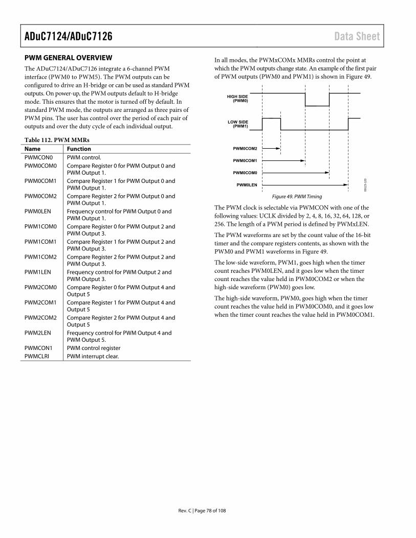
ADuC7124/ADuC7126 Data Sheet
Rev. C | Page 78 of 108
PWM GENERAL OVERVIEW The ADuC7124/ADuC7126 integrate a 6-channel PWM interface (PWM0 to PWM5). The PWM outputs can be configured to drive an H-bridge or can be used as standard PWM outputs. On power-up, the PWM outputs default to H-bridge mode. This ensures that the motor is turned off by default. In standard PWM mode, the outputs are arranged as three pairs of PWM pins. The user has control over the period of each pair of outputs and over the duty cycle of each individual output.
Table 112. PWM MMRs Name Function PWMCON0 PWM control. PWM0COM0 Compare Register 0 for PWM Output 0 and
PWM Output 1. PWM0COM1 Compare Register 1 for PWM Output 0 and
PWM Output 1. PWM0COM2 Compare Register 2 for PWM Output 0 and
PWM Output 1. PWM0LEN Frequency control for PWM Output 0 and
PWM Output 1. PWM1COM0 Compare Register 0 for PWM Output 2 and
PWM Output 3. PWM1COM1 Compare Register 1 for PWM Output 2 and
PWM Output 3. PWM1COM2 Compare Register 2 for PWM Output 2 and
PWM Output 3. PWM1LEN Frequency control for PWM Output 2 and
PWM Output 3. PWM2COM0 Compare Register 0 for PWM Output 4 and
Output 5 PWM2COM1 Compare Register 1 for PWM Output 4 and
Output 5 PWM2COM2 Compare Register 2 for PWM Output 4 and
Output 5 PWM2LEN Frequency control for PWM Output 4 and
PWM Output 5. PWMCON1 PWM control register PWMCLRI PWM interrupt clear.
In all modes, the PWMxCOMx MMRs control the point at which the PWM outputs change state. An example of the first pair of PWM outputs (PWM0 and PWM1) is shown in Figure 49.
HIGH SIDE(PWM0)
LOW SIDE(PWM1)
PWM0COM2
PWM0COM1
PWM0COM0
PWM0LEN
0912
3-12
0
Figure 49. PWM Timing
The PWM clock is selectable via PWMCON with one of the following values: UCLK divided by 2, 4, 8, 16, 32, 64, 128, or 256. The length of a PWM period is defined by PWMxLEN.
The PWM waveforms are set by the count value of the 16-bit timer and the compare registers contents, as shown with the PWM0 and PWM1 waveforms in Figure 49.
The low-side waveform, PWM1, goes high when the timer count reaches PWM0LEN, and it goes low when the timer count reaches the value held in PWM0COM2 or when the high-side waveform (PWM0) goes low.
The high-side waveform, PWM0, goes high when the timer count reaches the value held in PWM0COM0, and it goes low when the timer count reaches the value held in PWM0COM1.

Data Sheet ADuC7124/ADuC7126
Rev. C | Page 79 of 108
Table 113. PWMCON0 MMR Bit Descriptions Bit Name Description 14 SYNC Enables PWM synchronization. Set to 1 by the user so that all PWM counters are reset on the next clock edge after the detection of a high-to-low
transition on the P3.7/PWMSYNC pin. Cleared by the user to ignore transitions on the P3.7/PWMSYNC pin. 13 PWM5INV Set to 1 by the user to invert PWM5. Cleared by the user to use PWM5 in normal mode. 12 PWM3INV Set to 1 by the user to invert PWM3. Cleared by the user to use PWM3 in normal mode. 11 PWM1INV Set to 1 by the user to invert PWM1. Cleared by the user to use PWM1 in normal mode. 10 PWMTRIP Set to 1 by the user to enable PWM trip interrupt. When the PWM trip input (Pin P3.6/PWMTRIP or Pin P0.4/PWMTRIP)
is low, the PWMEN bit is cleared and an interrupt is generated. Cleared by the user to disable the PWMTRIP interrupt. 9 ENA If HOFF = 0 and HMODE = 1; note that, if not in H-bridge mode, this bit has no effect. Set to 1 by the user to enable PWM outputs. Cleared by the user to disable PWM outputs. If HOFF = 1 and HMODE = 1, see Table 114.
PWMCP[2:0] PWM clock prescaler bits. Sets the UCLK divider. [000] = UCLK/2. [001] = UCLK/4. [010] = UCLK/8. [011] = UCLK/16. [100] = UCLK/32. [101] = UCLK/64. [110] = UCLK/128.
[8:6]
[111] = UCLK/256. 5 POINV Set to 1 by the user to invert all PWM outputs. Cleared by the user to use PWM outputs as normal. 4 HOFF High side off. Set to 1 by the user to force PWM0 and PWM2 outputs high. This also forces PWM1 and PWM3 low. Cleared by the user to use the PWM outputs as normal. 3 LCOMP Load compare registers. Set to 1 by the user to load the internal compare registers with the values in PWMxCOMx on the next transition of
the PWM timer from 0x00 to 0x01. Cleared by the user to use the values previously stored in the internal compare registers. 2 DIR Direction control. Set to 1 by the user to enable PWM0 and PWM1 as the output signals while PWM2 and PWM3 are held low. Cleared by the user to enable PWM2 and PWM3 as the output signals while PWM0 and PWM1 are held low. 1 HMODE Enables H-bridge mode.1
Set to 1 by the user to enable H-bridge mode and Bit 1 to Bit 5 of PWMCON. Cleared by the user to operate the PWMs in standard mode. 0 PWMEN Set to 1 by the user to enable all PWM outputs. Cleared by the user to disable all PWM outputs. 1 In H-bridge mode, HMODE = 1. See Table 114 to determine the PWM outputs.
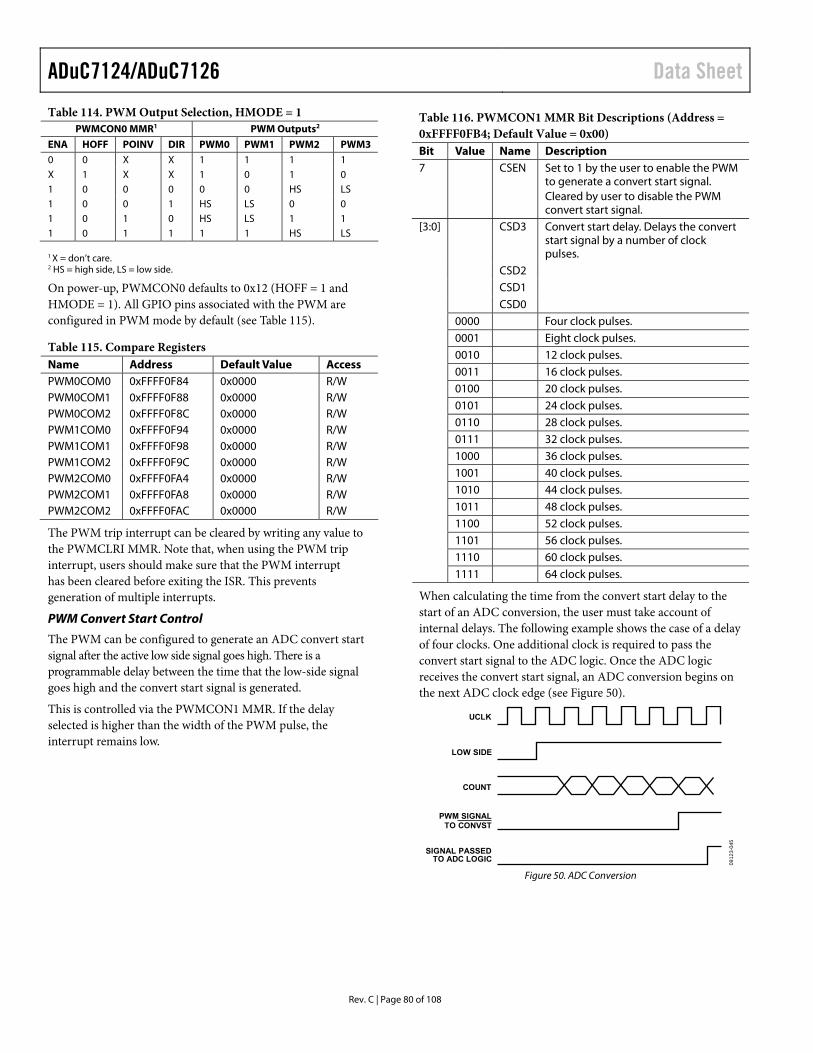
ADuC7124/ADuC7126 Data Sheet
Rev. C | Page 80 of 108
Table 114. PWM Output Selection, HMODE = 1 PWMCON0 MMR1 PWM Outputs2
ENA HOFF POINV DIR PWM0 PWM1 PWM2 PWM3
0 0 X X 1 1 1 1 X 1 X X 1 0 1 0 1 0 0 0 0 0 HS LS 1 0 0 1 HS LS 0 0 1 0 1 0 HS LS 1 1 1 0 1 1 1 1 HS LS
1 X = don’t care. 2 HS = high side, LS = low side.
On power-up, PWMCON0 defaults to 0x12 (HOFF = 1 and HMODE = 1). All GPIO pins associated with the PWM are configured in PWM mode by default (see Table 115).
Table 115. Compare Registers Name Address Default Value Access PWM0COM0 0xFFFF0F84 0x0000 R/W PWM0COM1 0xFFFF0F88 0x0000 R/W PWM0COM2 0xFFFF0F8C 0x0000 R/W PWM1COM0 0xFFFF0F94 0x0000 R/W PWM1COM1 0xFFFF0F98 0x0000 R/W PWM1COM2 0xFFFF0F9C 0x0000 R/W PWM2COM0 0xFFFF0FA4 0x0000 R/W PWM2COM1 0xFFFF0FA8 0x0000 R/W PWM2COM2 0xFFFF0FAC 0x0000 R/W
The PWM trip interrupt can be cleared by writing any value to the PWMCLRI MMR. Note that, when using the PWM trip interrupt, users should make sure that the PWM interrupt has been cleared before exiting the ISR. This prevents generation of multiple interrupts.
PWM Convert Start Control
The PWM can be configured to generate an ADC convert start signal after the active low side signal goes high. There is a programmable delay between the time that the low-side signal goes high and the convert start signal is generated.
This is controlled via the PWMCON1 MMR. If the delay selected is higher than the width of the PWM pulse, the interrupt remains low.
Table 116. PWMCON1 MMR Bit Descriptions (Address = 0xFFFF0FB4; Default Value = 0x00) Bit Value Name Description 7 CSEN Set to 1 by the user to enable the PWM
to generate a convert start signal. Cleared by user to disable the PWM convert start signal.
CSD3 Convert start delay. Delays the convert start signal by a number of clock pulses.
CSD2 CSD1 CSD0 0000 Four clock pulses. 0001 Eight clock pulses. 0010 12 clock pulses. 0011 16 clock pulses. 0100 20 clock pulses. 0101 24 clock pulses. 0110 28 clock pulses. 0111 32 clock pulses. 1000 36 clock pulses. 1001 40 clock pulses. 1010 44 clock pulses. 1011 48 clock pulses. 1100 52 clock pulses. 1101 56 clock pulses. 1110 60 clock pulses.
[3:0]
1111 64 clock pulses.
When calculating the time from the convert start delay to the start of an ADC conversion, the user must take account of internal delays. The following example shows the case of a delay of four clocks. One additional clock is required to pass the convert start signal to the ADC logic. Once the ADC logic receives the convert start signal, an ADC conversion begins on the next ADC clock edge (see Figure 50).
UCLK
LOW SIDE
COUNT
PWM SIGNAL
SIGNAL PASSEDTO ADC LOGIC
TO CONVST
0912
3-04
5
Figure 50. ADC Conversion
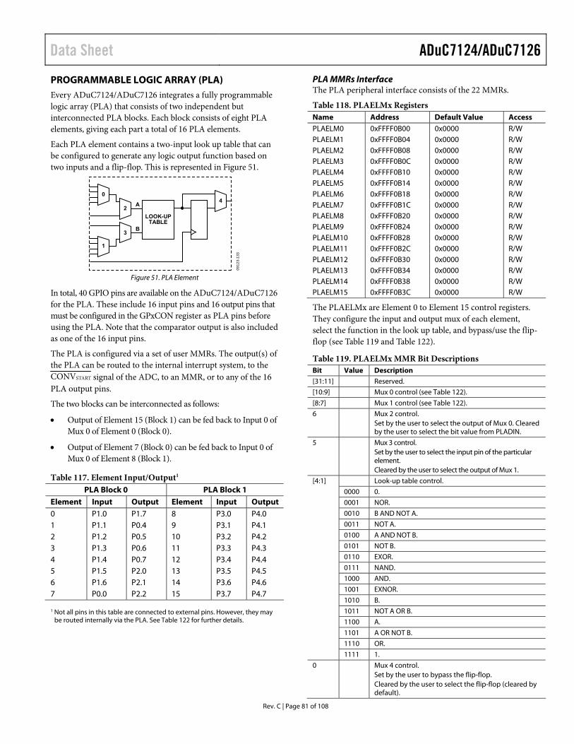
Data Sheet ADuC7124/ADuC7126
Rev. C | Page 81 of 108
PROGRAMMABLE LOGIC ARRAY (PLA) Every ADuC7124/ADuC7126 integrates a fully programmable logic array (PLA) that consists of two independent but interconnected PLA blocks. Each block consists of eight PLA elements, giving each part a total of 16 PLA elements.
Each PLA element contains a two-input look up table that can be configured to generate any logic output function based on two inputs and a flip-flop. This is represented in Figure 51.
0912
3-13
3
42
0
1
3
A
B
LOOK-UPTABLE
Figure 51. PLA Element
In total, 40 GPIO pins are available on the ADuC7124/ADuC7126 for the PLA. These include 16 input pins and 16 output pins that must be configured in the GPxCON register as PLA pins before using the PLA. Note that the comparator output is also included as one of the 16 input pins.
The PLA is configured via a set of user MMRs. The output(s) of the PLA can be routed to the internal interrupt system, to the CONVSTART signal of the ADC, to an MMR, or to any of the 16 PLA output pins.
The two blocks can be interconnected as follows:
• Output of Element 15 (Block 1) can be fed back to Input 0 of Mux 0 of Element 0 (Block 0).
• Output of Element 7 (Block 0) can be fed back to Input 0 of Mux 0 of Element 8 (Block 1).
Table 117. Element Input/Output1 PLA Block 0 PLA Block 1
Element Input Output Element Input Output 0 P1.0 P1.7 8 P3.0 P4.0 1 P1.1 P0.4 9 P3.1 P4.1 2 P1.2 P0.5 10 P3.2 P4.2 3 P1.3 P0.6 11 P3.3 P4.3 4 P1.4 P0.7 12 P3.4 P4.4 5 P1.5 P2.0 13 P3.5 P4.5 6 P1.6 P2.1 14 P3.6 P4.6 7 P0.0 P2.2 15 P3.7 P4.7 1 Not all pins in this table are connected to external pins. However, they may
be routed internally via the PLA. See Table 122 for further details.
PLA MMRs Interface The PLA peripheral interface consists of the 22 MMRs.
Table 118. PLAELMx Registers Name Address Default Value Access PLAELM0 0xFFFF0B00 0x0000 R/W PLAELM1 0xFFFF0B04 0x0000 R/W PLAELM2 0xFFFF0B08 0x0000 R/W PLAELM3 0xFFFF0B0C 0x0000 R/W PLAELM4 0xFFFF0B10 0x0000 R/W PLAELM5 0xFFFF0B14 0x0000 R/W PLAELM6 0xFFFF0B18 0x0000 R/W PLAELM7 0xFFFF0B1C 0x0000 R/W PLAELM8 0xFFFF0B20 0x0000 R/W PLAELM9 0xFFFF0B24 0x0000 R/W PLAELM10 0xFFFF0B28 0x0000 R/W PLAELM11 0xFFFF0B2C 0x0000 R/W PLAELM12 0xFFFF0B30 0x0000 R/W PLAELM13 0xFFFF0B34 0x0000 R/W PLAELM14 0xFFFF0B38 0x0000 R/W PLAELM15 0xFFFF0B3C 0x0000 R/W
The PLAELMx are Element 0 to Element 15 control registers. They configure the input and output mux of each element, select the function in the look up table, and bypass/use the flip-flop (see Table 119 and Table 122).
Table 119. PLAELMx MMR Bit Descriptions Bit Value Description
[31:11] Reserved.
[10:9] Mux 0 control (see Table 122).
[8:7] Mux 1 control (see Table 122).
6 Mux 2 control. Set by the user to select the output of Mux 0. Cleared by the user to select the bit value from PLADIN.
5 Mux 3 control. Set by the user to select the input pin of the particular element. Cleared by the user to select the output of Mux 1.
[4:1] Look-up table control.
0000 0.
0001 NOR.
0010 B AND NOT A.
0011 NOT A.
0100 A AND NOT B.
0101 NOT B.
0110 EXOR.
0111 NAND.
1000 AND.
1001 EXNOR.
1010 B.
1011 NOT A OR B.
1100 A.
1101 A OR NOT B.
1110 OR.
1111 1.
0 Mux 4 control. Set by the user to bypass the flip-flop. Cleared by the user to select the flip-flop (cleared by default).
ADuC7124/ADuC7126 Data Sheet
Rev. C | Page 82 of 108
PLACLK Register
Name: PLACLK
Address: 0xFFFF0B40
Default Value: 0x00
Access: Read/write
PLACLK is the clock selection for the flip-flops of Block 0 and Block 1. Note that the maximum frequency when using the GPIO pins as the clock input for the PLA blocks is 41.78 MHz.
Table 120. PLACLK MMR Bit Descriptions Bit Value Description 7 Reserved. [6:4] Block 1 clock source selection.
000 GPIO clock on P0.5. 001 GPIO clock on P0.0. 010 GPIO clock on P0.7. 011 HCLK. 100 OCLK (32.768 kHz). 101 Timer1 overflow. 110 UCLK. 111 Internal 32,768 oscillator.
3 Reserved. [2:0] Block 0 clock source selection.
000 GPIO clock on P0.5. 001 GPIO clock on P0.0. 010 GPIO clock on P0.7. 011 HCLK. 100 OCLK (32.768 kHz). 101 Timer1 overflow. Other Reserved.
PLAIRQ Register
Name: PLAIRQ
Address: 0xFFFF0B44
Default Value: 0x00000000
Access: Read/write
PLAIRQ enables IRQ0 and/or IRQ1 and selects the source of the IRQ.
Table 121. PLAIRQ MMR Bit Descriptions Bit Value Description
[15:13] Reserved. 12 PLA IRQ1 enable bit.
Set by the user to enable IRQ1 output from PLA. Cleared by the user to disable IRQ1 output from PLA.
[11:8] PLA IRQ1 source. 0000 PLA Element 0. 0001 PLA Element 1. 1111 PLA Element 15. [7:5] Reserved. 4 PLA IRQ0 enable bit.
Set by the user to enable IRQ0 output from PLA. Cleared by the user to disable IRQ0 output from PLA.
[3:0] PLA IRQ0 source. 0000 PLA Element 0. 0001 PLA Element 1. 1111 PLA Element 15.
Table 122. Feedback Configuration Bit Value PLAELM0 PLAELM1 to PLAELM7 PLAELM8 PLAELM9 to PLAELM15 [10:9] 00 Element 15 Element 0 Element 7 Element 8 01 Element 2 Element 2 Element 10 Element 10 10 Element 4 Element 4 Element 12 Element 12 11 Element 6 Element 6 Element 14 Element 14 [8:7] 00 Element 1 Element 1 Element 9 Element 9 01 Element 3 Element 3 Element 11 Element 11 10 Element 5 Element 5 Element 13 Element 13 11 Element 7 Element 7 Element 15 Element 15
Data Sheet ADuC7124/ADuC7126
Rev. C | Page 83 of 108
PLAADC Register
Name: PLAADC
Address: 0xFFFF0B48
Default Value: 0x00000000
Access: Read/write
PLAADC is the PLA source for the ADC start conversion signal.
Table 123. PLAADC MMR Bit Descriptions Bit Value Description [31:5] Reserved. 4 ADC start conversion enable bit.
Set by the user to enable ADC start conversion from PLA. Cleared by the user to disable ADC start conversion from PLA.
[3:0] ADC start conversion source. 0000 PLA Element 0. 0001 PLA Element 1. 1111 PLA Element 15.
PLADIN Register
Name: PLADIN
Address: 0xFFFF0B4C
Default Value: 0x00000000
Access: Read/write
PLADIN is a data input MMR for PLA.
Table 124. PLADIN MMR Bit Descriptions Bit Description [31:16] Reserved. [15:0] Input bit to Element 15 to Element 0.
PLADOUT Register
Name: PLADOUT
Address: 0xFFFF0B50
Default Value: 0x00000000
Access: Read only
PLADOUT is a data output MMR for PLA. This register is always updated.
Table 125. PLADOUT MMR Bit Descriptions Bit Description [31:16] Reserved. [15:0] Output bit from Element 15 to Element 0.
PLALCK Register
Name: PLALCK
Address: 0xFFFF0B54
Default Value: 0x00
Access: Write only
PLALCK is a PLA lock option. Bit 0 is written only once. When set, it does not allow modification of any of the PLA MMRs, except PLADIN. A PLA tool is provided in the development system to easily configure the PLA.

ADuC7124/ADuC7126 Data Sheet
Rev. C | Page 84 of 108
PROCESSOR REFERENCE PERIPHERALS INTERRUPT SYSTEM There are 25 interrupt sources on the ADuC7124/ADuC7126 that are controlled by the interrupt controller. All interrupts are generated from the on-chip peripherals, except for the software interrupt (SWI), which is programmable by the user. The ARM7TDMI CPU core recognizes interrupts as one of two types: a normal interrupt request (IRQ) and a fast interrupt request (FIQ). All the interrupts can be masked separately.
The control and configuration of the interrupt system is managed through a number of interrupt-related registers. The bits in each IRQ and FIQ register represent the same interrupt source as described in Table 126.
The ADuC7124/ADuC7126 contain a vectored interrupt control-ler (VIC) that supports nested interrupts up to eight levels. The VIC also allows the programmer to assign priority levels to all interrupt sources. Interrupt nesting must be enabled by setting the ENIRQN bit in the IRQCONN register. A number of extra MMRs are used when the full-vectored interrupt controller is enabled.
IRQSTA/FIQSTA should be saved immediately upon entering the interrupt service routine (ISR) to ensure that all valid interrupt sources are serviced.
Table 126. IRQ/FIQ MMRs Bit Descriptions Bit Description Comments 0 All interrupts OR’ed
(FIQ only) This bit is set if any FIQ is active.
1 Software interrupt User programmable interrupt source.
2 Timer0 General-Purpose Timer 0. 3 Timer1 General-Purpose Timer 1. 4 Timer2 or wake-up
timer General-Purpose Timer 2 or wake-up timer.
5 Timer3 or watchdog timer
General-Purpose Timer 3 or watchdog timer.
6 Flash Control 0 Flash controller for Block 0 interrupt.
7 Flash Control 1 Flash controller for Block 1 interrupt.
8 ADC ADC interrupt source bit. 9 UART0 UART0 interrupt source bit. 10 UART1 UART1 interrupt source bit. 11 PLL lock PLL lock bit. 12 I2C0 master IRQ I2C master interrupt source bit. 13 I2C0 slave IRQ I2C slave interrupt source bit. 14 I2C1 master IRQ I2C master interrupt source bit. 15 I2C1 slave IRQ I2C slave interrupt source bit. 16 SPI SPI interrupt source bit. 17 XIRQ0 (GPIO IRQ0 ) External Interrupt 0. 18 Comparator Voltage comparator source bit. 19 PSM Power supply monitor. 20 XIRQ1 (GPIO IRQ1) External Interrupt 1.
Bit Description Comments 21 PLA IRQ0 PLA Block 0 IRQ bit. 22 XIRQ2 (GPIO IRQ2 ) External Interrupt 2. 23 XIRQ3 (GPIO IRQ3) External Interrupt 3. 24 PLA IRQ1 PLA Block 1 IRQ bit. 25 PWM PWM trip interrupt source bit.
IRQ The IRQ is the exception signal to enter the IRQ mode of the processor. It services general-purpose interrupt handling of internal and external events.
All 32 bits are logically OR’ed to create a single IRQ signal to the ARM7TDMI core. Descriptions of the four 32-bit registers dedicated to IRQ follow.
IRQSTA Register
IRQSTA is a read-only register that provides the current-enabled IRQ source status (effectively a logic AND of the IRQSIG and IRQEN bits). When set to 1, that source generates an active IRQ request to the ARM7TDMI core. There is no priority encoder or interrupt vector generation. This function is implemented in software in a common interrupt handler routine.
IRQSTA Register
Name: IRQSTA
Address: 0xFFFF0000
Default Value: 0x00000000
Access: Read only
IRQSIG Register
IRQSIG reflects the status of the various IRQ sources. If a periph-eral generates an IRQ signal, the corresponding bit in the IRQSIG is set; otherwise, it is cleared. The IRQSIG bits clear when the interrupt in the particular peripheral is cleared. All IRQ sources can be masked in the IRQEN MMR. IRQSIG is read only. This register should not be used in an interrupt service routine for determining the source of an IRQ exception; IRQSTA should only be used for this purpose.
IRQSIG Register
Name: IRQSIG
Address: 0xFFFF0004
Default Value: 0x00000000
Access: Read only

Data Sheet ADuC7124/ADuC7126
Rev. C | Page 85 of 108
IRQEN Register
IRQEN provides the value of the current enable mask. When a bit is set to 1, the corresponding source request is enabled to create an IRQ exception. When a bit is set to 0, the correspond-ing source request is disabled or masked, which does not create an IRQ exception. The IRQEN register cannot be used to disable an interrupt.
IRQEN Register
Name: IRQEN
Address: 0xFFFF0008
Default Value: 0x00000000
Access: Read/write
IRQCLR Register
IRQCLR is a write-only register that allows the IRQEN register to clear to mask an interrupt source. Each bit that is set to 1 clears the corresponding bit in the IRQEN register without affecting the remaining bits. The pair of registers, IRQEN and IRQCLR, allow independent manipulation of the enable mask without requiring an atomic read-modify-write.
This register should be used to disable an interrupt source only during the following conditions:
• In the interrupt sources interrupt service routine. • When the peripheral is temporarily disabled by its own
control register.
This register should not be used to disable an IRQ source if that IRQ source has an interrupt pending or may have an interrupt pending.
IRQCLR Register
Name: IRQCLR
Address: 0xFFFF000C
Default Value: 0x00000000
Access: Write only
FAST INTERRUPT REQUEST (FIQ) The fast interrupt request (FIQ) is the exception signal to enter the FIQ mode of the processor. It is provided to service data transfer or communication channel tasks with low latency. The FIQ interface is identical to the IRQ interface and provides the second level interrupt (highest priority). Four 32-bit registers are dedicated to FIQ: FIQSIG, FIQEN, FIQCLR, and FIQSTA.
Bit 31 to Bit 1 of FIQSTA are logically OR’ed to create the FIQ signal to the core and to Bit 0 of both the FIQ and IRQ registers (FIQ source).
The logic for FIQEN and FIQCLR does not allow an interrupt source to be enabled in both IRQ and FIQ masks. A bit set to 1 in FIQEN clears, as a side effect, the same bit in IRQEN.
Likewise, a bit set to 1 in IRQEN clears, as a side effect, the same bit in FIQEN. An interrupt source can be disabled in both the IRQEN and FIQEN masks.
FIQSIG
FIQSIG reflects the status of the different FIQ sources. If a peripheral generates an FIQ signal, the corresponding bit in the FIQSIG is set; otherwise, it is cleared. The FIQSIG bits are cleared when the interrupt in the particular peripheral is cleared. All FIQ sources can be masked in the FIQEN MMR. FIQSIG is read only.
FIQSIG Register
Name: FIQSIG
Address: 0xFFFF0104
Default Value: 0x00000000
Access: Read only
FIQEN
FIQEN provides the value of the current enable mask. When a bit is set to 1, the corresponding source request is enabled to create an FIQ exception. When a bit is set to 0, the correspond-ing source request is disabled or masked, which does not create an FIQ exception. The FIQEN register cannot be used to disable an interrupt.
FIQEN Register
Name: FIQEN
Address: 0xFFFF0108
Default Value: 0x00000000
Access: Read/write
FIQCLR
FIQCLR is a write-only register that allows the FIQEN register to clear to mask an interrupt source. Each bit that is set to 1 clears the corresponding bit in the FIQEN register without affecting the remaining bits. The pair of registers, FIQEN and FIQCLR, allows independent manipulation of the enable mask without requiring an atomic read-modify-write.
This register should be used to disable an interrupt source only during the following conditions:
• In the interrupt sources interrupt service routine. • The peripheral is temporarily disabled by its own control
register.
This register should not be used to disable an IRQ source if that IRQ source has an interrupt pending or may have an interrupt pending.

ADuC7124/ADuC7126 Data Sheet
Rev. C | Page 86 of 108
FIQCLR Register
Name: FIQCLR
Address: 0xFFFF010C
Default Value: 0x00000000
Access: Write only
FIQSTA
FIQSTA is a read-only register that provides the current enabled FIQ source status (effectively a logic AND of the FIQSIG and FIQEN bits). When set to 1, that source generates an active FIQ request to the ARM7TDMI core. There is no priority encoder or interrupt vector generation. This function is implemented in software in a common interrupt handler routine.
FIQSTA Register
Name: FIQSTA
Address: 0xFFFF0100
Default Value: 0x00000000
Access: Read only
Programmed Interrupts
Because the programmed interrupts are not maskable, they are controlled by another register (SWICFG) that writes into the IRQSTA and IRQSIG registers and/or the FIQSTA and FIQSIG registers at the same time.
The 32-bit register dedicated to software interrupt is SWICFG (described in Table 127). This MMR allows control of a pro-grammed source interrupt.
Table 127. SWICFG MMR Bit Descriptions Bit Description [31:3] Reserved. 2 Programmed interrupt FIQ. Setting/clearing this bit
corresponds to setting/clearing Bit 1 of FIQSTA and FIQSIG.
1 Programmed interrupt IRQ. Setting/clearing this bit corresponds to setting/clearing Bit 1 of IRQSTA and IRQSIG.
0 Reserved.
Any interrupt signal must be active for at least the minimum interrupt latency time to be detected by the interrupt controller and to be detected by the user in the IRQSTA/FIQSTA register.
INTERNALARBITER
LOGIC
BITS[31:23]UNUSED
BITS[22:7](IRQBASE)
BITS[6:2]HIGHESTPRIORITY
ACTIVE IRQ
BITS[1:0]LSBs
IRQ_SOURCE POINTERFUNCTION(IRQVEC)FIQ_SOURCE
INTERRUPT VECTOR
PROGRAMMABLE PRIORITYPER INTERRUT
(IRQP0/IRQP1/IRQP2/IRQP3)
0912
3-05
4
Figure 52. Interrupt Structure
VECTORED INTERRUPT CONTROLLER (VIC) The ADUC7124/ADuC7126 incorporate an enhanced interrupt control system or (vectored interrupt controller). The vectored interrupt controller for IRQ interrupt sources is enabled by set-ting Bit 0 of the IRQCONN register. Similarly, Bit 1 of IRQCONN enables the vectored interrupt controller for the FIQ interrupt sources. The vectored interrupt controller provides the following enhancements to the standard IRQ/FIQ interrupts:
• Vectored interrupts—allows a user to define separate interrupt service routine addresses for every interrupt source. This is achieved by using the IRQBASE and IRQVEC registers.
• IRQ/FIQ interrupts—can be nested up to eight levels depending on the priority settings. An FIQ still has a higher priority than an IRQ. Therefore, if the VIC is enabled for both the FIQ and IRQ and prioritization is maximized, it is possible to have 16 separate interrupt levels.
• Programmable interrupt priorities—using the IRQP0 to IRQP3 registers, an interrupt source can be assigned an interrupt priority level value between 0 and 7.
VIC MMRs
IRQBASE Register
The vector base register, IRQBASE, is used to point to the start address of memory used to store 32 pointer addresses. These pointer addresses are the addresses of the individual interrupt service routines.
Name: IRQBASE
Address: 0xFFFF0014
Default Value: 0x00000000
Access: Read/write
Table 128. IRQBASE MMR Bit Descriptions Bit Type Initial Value Description [31:16] Read only Reserved Always read as 0. [15:0] R/W 0 Vector base address.

Data Sheet ADuC7124/ADuC7126
Rev. C | Page 87 of 108
IRQVEC Register
The IRQ interrupt vector register, IRQVEC points to a memory address containing a pointer to the interrupt service routine of the currently active IRQ. This register should only be read when an IRQ occurs and IRQ interrupt nesting has been enabled by setting Bit 0 of the IRQCONN register.
Name: IRQVEC
Address: 0xFFFF001C
Default Value: 0x00000000
Access: Read only
Table 129. IRQVEC MMR Bit Descriptions
Bit Type Initial Value Description
[31:23] R 0 Always read as 0. [22:7] R/W 0 IRQBASE register value. [6:2] R 0 Highest priority source. This is a
value between 0 and 27 represent-ing the possible interrupt sources. For example, if the highest currently active IRQ is Timer 2, then these bits are [00100].
[1:0] Reserved
0 Reserved bits.
Priority Registers
The IRQ interrupt vector register, IRQVEC points to a memory address containing a pointer to the interrupt service routine of the currently active IRQ. This register should only be read when an IRQ occurs and IRQ interrupt nesting has been enabled by setting Bit 0 of the IRQCONN register.
IRQP0 Register
Name: IRQP0
Address: 0xFFFF0020
Default Value: 0x00000000
Access: Read/write
Table 130. IRQP0 MMR Bit Descriptions Bit Name Description 31 Reserved. [30:28] Flash1PI A priority level of 0 to 7 can be set for the
Flash Block 1 controller interrupt source. 27 Reserved. [26:24] Flash0PI A priority level of 0 to 7 can be set for the
Flash Block 0 controller interrupt source. 23 Reserved. [22:20] T3PI A priority level of 0 to 7 can be set for
Timer 3. 19 Reserved.
Bit Name Description [18:16] T2PI A priority level of 0 to 7 can be set for
Timer2. 15 Reserved. [14:12] T1PI A priority level of 0 to 7 can be set for
Timer1. 11 Reserved. [10:8] T0PI A priority level of 0 to 7 can be set for
Timer0. 7 Reserved. [6:4] SWINTP A priority level of 0 to 7 can be set for the
software interrupt source. [3:0] Interrupt 0 cannot be prioritized.
IRQP1 Register
Name: IRQP1
Address: 0xFFFF0024
Default Value: 0x00000000
Access: Read/write
Table 131. IRQP1 MMR Bit Descriptions Bit Name Description 31 Reserved. [30:28] I2C1SPI A priority level of 0 to 7 can be set for the
I2C1 slave. 27 Reserved. [26:24] I2C1MPI A priority level of 0 to 7 can be set for the
I2C1 master. 23 Reserved. [22:20] I2C0SPI A priority level of 0 to 7 can be set for the
I2C0 slave. 19 Reserved. [18:16] I2C0MPI A priority level of 0 to 7 can be set for the
I2C 0 master. 15 Reserved. [14:12] PLLPI A priority level of 0 to 7 can be set for the
PLL lock interrupt. 11 Reserved. [10:8] UART1PI A priority level of 0 to 7 can be set for
UART1. 7 Reserved. [6:4] UART0PI A priority level of 0 to 7 can be set for
UART0. 5 Reserved. [2:0] ADCPI A priority level of 0 to 7 can be set for the
ADC interrupt source.
ADuC7124/ADuC7126 Data Sheet
Rev. C | Page 88 of 108
IRQP2 Register
Name: IRQP2
Address: 0xFFFF0028
Default Value: 0x00000000
Access: Read/write
Table 132. IRQP2 MMR Bit Descriptions Bit Name Description 31 Reserved. [30:28] IRQ3PI A priority level of 0 to 7 can be set for IRQ3. 27 Reserved. [26:24] IRQ2PI A priority level of 0 to 7 can be set for IRQ2. 23 Reserved. [22:20] PLA0PI A priority level of 0 to 7 can be set for PLA
IRQ0. 19 Reserved. [18:16] IRQ1PI A priority level of 0 to 7 can be set for IRQ1. 15 Reserved. [14:12] PSMPI A priority level of 0 to 7 can be set for the
power supply monitor interrupt source. 11 Reserved. [10:8] COMPI A priority level of 0 to 7 can be set for the
comparator. 7 Reserved. [6:4] IRQ0PI A priority level of 0 to 7 can be set for IRQ0. 3 Reserved. [2:0] SPIPI A priority level of 0 to 7 can be set for SPI.
IRQP3 Register
Name: IRQP3
Address: 0xFFFF002C
Default Value: 0x00000000
Access: Read/write
Table 133. IRQP3 MMR Bit Descriptions Bit Name Description [31:7] Reserved. [6:4] PWMPI A priority level of 0 to 7 can be set for PWM. 3 Reserved. [2:0] PLA1PI A priority level of 0 to 7 can be set for PLA
IRQ1.
IRQCONN Register
The IRQCONN register is the IRQ and FIQ control register. It contains two active bits: the first to enable nesting and prioritiza-tion of IRQ interrupts and the other to enable nesting and prioritization of FIQ interrupts.
If these bits are cleared, FIQs and IRQs can still be used, but it is not possible to nest IRQs or FIQs, nor is it possible to set an
interrupt source priority level. In this default state, an FIQ does have a higher priority than an IRQ.
Name: IRQCONN
Address: 0xFFFF0030
Default Value: 0x00000000
Access: Read/write
Table 134. IRQCONN MMR Bit Descriptions Bit Name Description 31:2 Reserved. These bits are reserved and should
not be written to. 1 ENFIQN Setting this bit to 1 enables nesting of FIQ
interrupts. Clearing this bit means no nesting or prioritization of FIQs is allowed.
0 ENIRQN Setting this bit to 1 enables nesting of IRQ interrupts. Clearing this bit means no nesting or prioritization of IRQs is allowed.
IRQSTAN Register
If IRQCONN Bit 0 is asserted and IRQVEC is read, one of the IRQSTAN[7:0] bits is asserted. The bit that asserts depends on the priority of the IRQ. If the IRQ is of Priority 0, then Bit 0 asserts, if Priority 1, then Bit 1 asserts, and so on. When a bit is set in this register, all interrupts of that priority and lower are blocked.
To clear a bit in this register, all bits of a higher priority must be cleared first. It is only possible to clear one bit at a time. For example, if this register is set to 0x09, writing 0xFF changes the register to 0x08, and writing 0xFF a second time changes the register to 0x00.
Name: IRQSTAN
Address: 0xFFFF003C
Default Value: 0x00000000
Access: Read/write
Table 135. IRQSTAN MMR Bit Descriptions Bit Name Description 31:8 Reserved. These bits are reserved and should
not be written to. 7:0 Setting these bits to 1 enables nesting of FIQ
interrupts. Clearing these bits means no nesting or prioritization of FIQs is allowed.
Data Sheet ADuC7124/ADuC7126
Rev. C | Page 89 of 108
FIQVEC Register
The FIQ interrupt vector register, FIQVEC, points to a memory address containing a pointer to the interrupt service routine of the currently active FIQ. This register should be read only when an FIQ occurs and FIQ interrupt nesting has been enabled by setting Bit 1 of the IRQCONN register.
Name: FIQVEC
Address: 0xFFFF011C
Default Value: 0x00000000
Access: Read only
Table 136. FIQVEC MMR Bit Descriptions
Bit Type Initial Value Description
[31:23] R 0 Always read as 0. [22:7] R/W 0 IRQBASE register value. [6:2] 0 Highest priority source. This is a
value between 0 and 27, representing the currently active interrupt source. The interrupts are listed in Table 126. For example, if the highest currently active FIQ is Timer2, then these bits are [00100].
[1:0] 0 Reserved.
FIQSTAN Register
If IRQCONN Bit 1 is asserted and FIQVEC is read, one of the FIQSTAN[7:0] bits is asserted. The bit that asserts depends on the priority of the FIQ. If the FIQ is of Priority 0, Bit 0 asserts, if Priority 1, Bit 1 asserts, and so forth.
When a bit is set in this register all interrupts of that priority and lower are blocked.
To clear a bit in this register, all bits of a higher priority must be cleared first. It is possible to clear only one bit at a time. For example, if this register is set to 0x09, then writing 0xFF
changes the register to 0x08 and writing 0xFF a second time changes the register to 0x00.
Name: FIQSTAN
Address: 0xFFFF013C
Default Value: 0x00000000
Access: Read/write
Table 137. FIQSTAN MMR Bit Descriptions Bit Name Description 31:8 Reserved. These bits are reserved and should
not be written to. 7:0 Setting this bit to 1 enables nesting of FIQ
interrupts. Clearing this bit means no nesting or prioritization of FIQs is allowed.
External Interrupts and PLA interrupts
The ADuC7124/ADuC7126 provide up to four external interrupt sources and two PLA interrupt sources. These external interrupts can be individually configured as level or rising/falling edge triggered.
To enable the external interrupt source or the PLA interrupt source, the appropriate bit must first be set in the FIQEN or IRQEN register. To select the required edge or level to trigger on, the IRQCONE register must be appropriately configured.
To properly clear an edge-based external IRQ interrupt or an edge-based PLA interrupt, set the appropriate bit in the IRQCLRE register.
IRQCONE Register
Name: IRQCONE
Address: 0xFFFF0034
Default Value: 0x00000000
Access: Read/write
Table 138. IRQCONE MMR Bit Descriptions Bit Value Name Description [31:12] Reserved. These bits are reserved and should not be written to. [11:10] 11 PLA1SRC[1:0] PLA IRQ1 triggers on falling edge. 10 PLA IRQ1 triggers on rising edge. 01 PLA IRQ1 triggers on low level. 00 PLA IRQ1 triggers on high level. [9:8] 11 IRQ3SRC[1:0] External IRQ3 triggers on falling edge. 10 External IRQ3 triggers on rising edge. 01 External IRQ3 triggers on low level. 00 External IRQ3 triggers on high level.

ADuC7124/ADuC7126 Data Sheet
Rev. C | Page 90 of 108
Bit Value Name Description [7:6] 11 IRQ2SRC[1:0] External IRQ2 triggers on falling edge. 10 External IRQ2 triggers on rising edge. 01 External IRQ2 triggers on low level. 00 External IRQ2 triggers on high level. [5:4] 11 PLA0SRC[1:0] PLA IRQ0 triggers on falling edge. 10 PLA IRQ0 triggers on rising edge. 01 PLA IRQ0 triggers on low level. 00 PLA IRQ0 triggers on high level. [3:2] 11 IRQ1SRC[1:0] External IRQ1 triggers on falling edge. 10 External IRQ1 triggers on rising edge. 01 External IRQ1 triggers on low level. 00 External IRQ1 triggers on high level. [1:0] 11 IRQ0SRC[1:0] External IRQ0 triggers on falling edge. 10 External IRQ0 triggers on rising edge. 01 External IRQ0 triggers on low level. 00 External IRQ0 triggers on high level.
IRQCLRE Register
Name: IRQCLRE
Address: 0xFFFF0038
Default Value: 0x00000000
Access: Write only
Table 139. IRQCLRE MMR Bit Descriptions Bit Name Description [31:25] Reserved. These bits are reserved and should not be written to. 24 PLA1CLRI A 1 must be written to this bit in the PLA IRQ1 interrupt service routine to clear an edge-
triggered PLA IRQ1 interrupt. 23 IRQ3CLRI A 1 must be written to this bit in the external IRQ3 interrupt service routine to clear an edge-
triggered IRQ3 interrupt. 22 IRQ2CLRI A 1 must be written to this bit in the external IRQ2 interrupt service routine to clear an edge-
triggered IRQ2 interrupt. 21 PLA0CLRI A 1 must be written to this bit in the PLA IRQ0 interrupt service routine to clear an edge-
triggered PLA IRQ0 interrupt. 20 IRQ1CLRI A 1 must be written to this bit in the external IRQ1 interrupt service routine to clear an edge-
triggered IRQ1 interrupt. [19:18] Reserved. These bits are reserved and should not be written to. 17 IRQ0CLRI A 1 must be written to this bit in the external IRQ0 interrupt service routine to clear an edge
triggered IRQ0 interrupt. [16:0] Reserved. These bits are reserved and should not be written to.

Data Sheet ADuC7124/ADuC7126
Rev. C | Page 91 of 108
TIMERS The ADuC7124/ADuC7126 have four general-purpose timers/counters.
• Timer0
• Timer1
• Timer2 or wake-up timer
• Timer3 or watchdog timer
These four timers in their normal mode of operation can be either free running or periodic.
In free-running mode, the counter decreases from the maxi-mum value until zero scale is reached and starts again at the minimum value. It also increases from the minimum value until full scale is reached and starts again at the maximum value.
In periodic mode, the counter decrements/increments from the value in the load register (TxLD MMR) until zero/full scale is reached and starts again at the value stored in the load register.
The timer interval is calculated as follows:
If the timer is set to count down, then
( )ClockSource
PrescalerTxLDInterval ×=
If the timer is set to count up, then
( )ClockSource
PrescalerTxLDFullScaleInterval
×=
-
The value of a counter can be read at any time by accessing its value register (TxVAL). Note that, when a timer is being clocked from a clock other than a core clock, an incorrect value may be read (due to asynchronous clock system). In this configuration, TxVAL should always be read twice. If the two readings are different, it should be read a third time to obtain the correct value.
Timers are started by writing in the control register of the corresponding timer (TxCON).
In normal mode, an IRQ is generated each time the value of the counter reaches zero when counting down. It is also generated each time the counter value reaches full scale when counting up. An IRQ can be cleared by writing any value to clear the register of that particular timer (TxCLRI).
When using an asynchronous clock-to-clock timer, the interrupt in the timer block can take more time to clear than the time it takes for the code in the interrupt routine to execute. Ensure that the interrupt signal is cleared before leaving the interrupt service routine. This can be done by checking the IRQSTA MMR.
Hr: Min: Sec: 1/128 Format
Timer 1 and Timer 2 have an Hr: Min: Sec: hundreds format. To use the timer in Hr: Min: Sec: hundreds format, the 32768 kHz clock and prescaler of 256 should be selected. The hundreds field does not represent milliseconds, but 1/128 of a second (256/32768).The bits representing the hour, minute, and second are not consecutive in the register. This arrange-ment applies to TxLD and TxVAL when using the Hr: Min: Sec: hundreds format as set in TxCON[5:4]. See Table 140 for more details.
Table 140. Hr: Min: Sec: Hundreds Format Bit Value Description [31:24] 0 to 23 or 0 to 255 hours [23:22] 0 reserved [21:16] 0 to 59 minutes [15:14] 0 reserved [13:8] 0 to 59 seconds 7 0 reserved [6:0] 0 to 127 1/128 of second

ADuC7124/ADuC7126 Data Sheet
Rev. C | Page 92 of 108
Timer0 (RTOS Timer)
Timer0 is a general-purpose, 16-bit timer (count down) with a programmable prescaler. The prescaler source is the core clock frequency (HCLK) and can be scaled by a factor of 1, 16, or 256.
Timer0 can be used to start ADC conversions, as shown in the block diagram in Figure 53.
0912
3-03
6
32.768kHzOSCILLATOR
UCLK
HCLK
PRESCALER÷1, 16, OR 256
16-BITDOWN
COUNTER
16-BITLOAD
TIMER0VALUE
TIMER0 IRQ
ADC CONVERSION
Figure 53. Timer0 Block Diagram
The Timer0 interface consists of four MMRs: T0LD, T0VAL, T0CON, and T0CLRI.
T0LD Register
Name: T0LD
Address: 0xFFFF0300
Default Value: 0x0000
Access: Read/write
T0LD is a 16-bit load register.
T0VAL Register
Name: T0VAL
Address: 0xFFFF0304
Default Value: 0xFFFF
Access: Read only
T0VAL is a 16-bit read-only register representing the current state of the counter.
T0CON Register
Name: T0CON
Address: 0xFFFF0308
Default Value: 0x0000
Access: Read/write
T0CON is the configuration MMR described in Table 141.

Data Sheet ADuC7124/ADuC7126
Rev. C | Page 93 of 108
Table 141. T0CON MMR Bit Descriptions Bit Value Description [31:8] Reserved. 7 Timer0 enable bit.
Set by the user to enable Timer0. Cleared by the user to disable Timer0 by default.
6 Timer0 mode. Set by the user to operate in periodic mode. Cleared by the user to operate in free-running mode. Default mode.
[5:4] Clock select bits. 00 HCLK. 01 UCLK. 10 32.768 kHz. 11 Reserved. [3:2] Prescale. 00 Core clock/1. Default value. 01 Core clock/16. 10 Core clock/256. 11 Undefined. Equivalent to 00. [1:0] Reserved.
T0CLRI Register
Name: T0CLRI
Address: 0xFFFF030C
Default Value: 0xFF
Access: Write only
T0CLRI is an 8-bit register. Writing any value to this register clears the interrupt.
Timer1 (General-Purpose Timer)
Timer1 is a general-purpose, 32-bit timer (count down or count up) with a programmable prescaler. The source can be the 32 kHz external crystal, the undivided system, the core clock, or P1.1 (maximum frequency 41.78 MHz). This source can be scaled by a factor of 1, 16, 256, or 32,768.
The counter can be formatted as a standard 32-bit value or as hours: minutes: seconds: hundredths.
Timer1 has a capture register (T1CAP) that can be triggered by a selected IRQ source initial assertion. This feature can be used to determine the assertion of an event more accurately than the precision allowed by the RTOS timer when the IRQ is serviced.
Timer1 can be used to start ADC conversions.
0912
3-13
7
32kHz OSCILLATORHCLKUCLK
P1.0
IRQ[19:0]
PRESCALER÷1, 16, 256,OR 32,768
32-BITUP/DOWNCOUNTER
32-BITLOAD
TIMER1VALUE
CAPTURE
TIMER1 IRQ
ADC CONVERSION
Figure 54. Timer1 Block Diagram
The Timer1 interface consists of five MMRs: T1LD, T1VAL, T1CON, T1CLRI, and T1CAP.
T1LD Register
Name: T1LD
Address: 0xFFFF0320
Default Value: 0x00000000
Access: Read/write
T1LD is a 32-bit load register.
T1VAL Register
Name: T1VAL
Address: 0xFFFF0324
Default Value: 0xFFFFFFFF
Access: Read only
T1VAL is a 32-bit read-only register that represents the current state of the counter.
T1CON Register
Name: T1CON
Address: 0xFFFF0328
Default Value: 0x0000
Access: Read/write
T1CON is the configuration MMR described in Table 142.
ADuC7124/ADuC7126 Data Sheet
Rev. C | Page 94 of 108
Table 142. T1CON MMR Bit Descriptions Bit Value Description [31:18] Reserved. 17 Event select bit.
Set by user to enable time capture of an event. Cleared by the user to disable time capture of an event.
[16:12] Event select range, 0 to 25. These events are as described in Table 126. All events are offset by two, that is, Event 2 in Table 126 becomes Event 0 for the purposes of Timer0.
[11:9] Clock select. 000 Core clock (41 MHz/2CD). 001 32.768 kHz. 010 UCLK. 011 P1.0 raising edge triggered. 8 Count up.
Set by the user for Timer1 to count up. Cleared by the user for Timer1 to count down by default.
7 Timer1 enable bit. Set by the user to enable Timer1. Cleared by the user to disable Timer1 by default.
6 Timer1 mode. Set by the user to operate in periodic mode. Cleared by the user to operate in free-running mode. Default mode.
[5:4] Format. 00 Binary. 01 Reserved. 10 Hr: min: sec: hundredths (23 hours to 0 hour). 11 Hr: min: sec: hundredths (255 hours to 0 hour). [3:0] Prescale. 0000 Source clock/1. 0100 Source clock/16. 1000 Source clock/256. 1111 Source clock/32,768.
T1CLRI Register
Name: T1CLRI
Address: 0xFFFF032C
Default Value: 0xFF
Access: Write only
T1CLRI is an 8-bit register. Writing any value to this register clears the Timer1 interrupt.
T1CAP Register
Name: T1CAP
Address: 0xFFFF0330
Default Value: 0x00000000
Access: Read/write
T1CAP is a 32-bit register. It holds the value contained in T1VAL when a particular event occurrs. This event must be selected in T1CON.
Timer2 (Wake-Up Timer)
Timer2 is a 32-bit wake-up timer, count down or count up, with a programmable prescaler. The prescaler is clocked directly from one of four clock sources, including the core clock (default selec-tion), the internal 32.768 kHz oscillator, the external 32.768 kHz watch crystal, or the PLL undivided clock. The selected clock source can be scaled by a factor of 1, 16, 256, or 32,768. The wake-up timer continues to run when the core clock is disabled. This gives a minimum resolution of 22 ns when the core is operating at 41.78 MHz and with a prescaler of 1. Capture of the current timer value is enabled if the Timer2 interrupt is enabled via IRQEN[4] (see Table 126).
The counter can be formatted as a plain 32-bit value or as hours: minutes: seconds: hundredths.
Timer2 reloads the value from T2LD either when Timer2 overflows or immediately when T2CLRI is written.
The Timer2 interface consists of four MMRs, shown in Table 143.
Table 143. Timer2 Interface Registers Register Description T2LD 32-bit register. Holds 32-bit unsigned integers. T2VAL 32-bit register. Holds 32-bit unsigned integers. This
register is read only. T2CLRI 8-bit register. Writing any value to this register clears
the Timer2 interrupt. T2CON Configuration MMR.
Timer2 Load Registers
Name: T2LD
Address: 0xFFFF0340
Default Value: 0x00000
Access: Read/write
T2LD is a 32-bit register, which holds the 32-bit value that is loaded into the counter.
Timer2 Clear Register
Name: T2CLRI
Address: 0xFFFF034C
Default Value: 0x00
Access: Write only
This 8-bit write-only MMR is written (with any value) by user code to refresh (reload) Timer2.

Data Sheet ADuC7124/ADuC7126
Rev. C | Page 95 of 108
Timer2 Value Register
Name: T2VAL
Address: 0xFFFF0344
Default Value: 0x0000
Access: Read only
T2VAL is a 32-bit register that holds the current value of Timer2.
Timer2 Control Register
Name: T2CON
Address: 0xFFFF0348
Default Value: 0x0000
Access: Read/write
This 32-bit MMR configures the mode of operation for Timer2.
Table 144. T2CON MMR Bit Descriptions Bit Value Description [31:11] Reserved. 10:9] Clock source select. 00 External 32.768 kHz watch crystal (default). 01 External 32.768 kHz watch crystal. 10 Internal 32.768 kHz oscillator. 11 HCLK. 8 Count up.
Set by the user for Timer2 to count up. Cleared by the user for Timer2 to count down (default).
7 Timer2 enable bit. Set by the user to enable Timer2. Cleared by the user to disable Timer2 (default).
6 Timer2 mode. Set by the user to operate in periodic mode. Cleared by the user to operate in free-running mode (default).
[5:4] Format. 00 Binary (default). 01 Reserved. 10 Hr: min: sec: hundredths (23 hours to 0 hours). 11 Hr: min: sec: hundredths (255 hours to 0 hours). [3:0] Prescaler. 0000 Source clock/1 (default). 0100 Source clock/16. 1000 Source clock/256. 1111 Source clock/32,768.
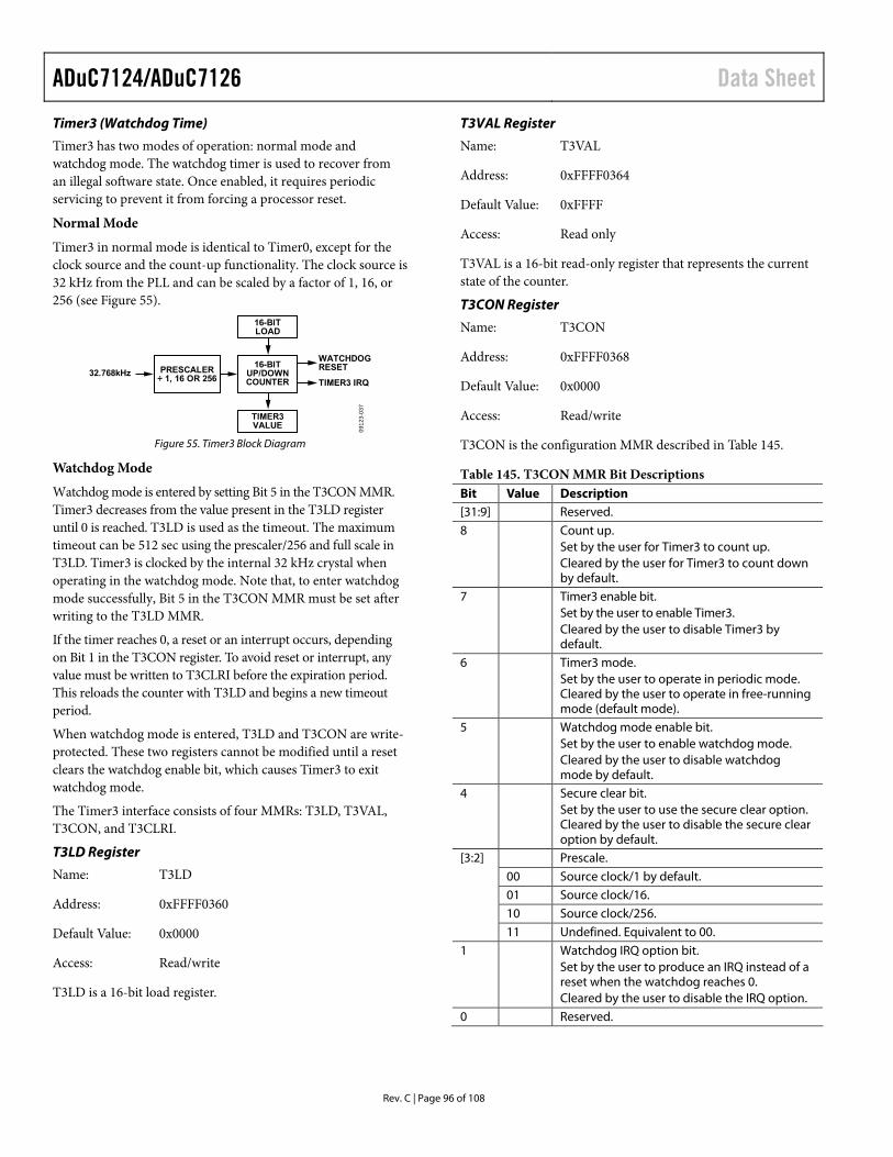
ADuC7124/ADuC7126 Data Sheet
Rev. C | Page 96 of 108
Timer3 (Watchdog Time)
Timer3 has two modes of operation: normal mode and watchdog mode. The watchdog timer is used to recover from an illegal software state. Once enabled, it requires periodic servicing to prevent it from forcing a processor reset.
Normal Mode
Timer3 in normal mode is identical to Timer0, except for the clock source and the count-up functionality. The clock source is 32 kHz from the PLL and can be scaled by a factor of 1, 16, or 256 (see Figure 55).
0912
3-03
7
32.768kHz PRESCALER÷ 1, 16 OR 256
16-BITUP/DOWNCOUNTER
16-BITLOAD
TIMER3VALUE
WATCHDOGRESET
TIMER3 IRQ
Figure 55. Timer3 Block Diagram
Watchdog Mode
Watchdog mode is entered by setting Bit 5 in the T3CON MMR. Timer3 decreases from the value present in the T3LD register until 0 is reached. T3LD is used as the timeout. The maximum timeout can be 512 sec using the prescaler/256 and full scale in T3LD. Timer3 is clocked by the internal 32 kHz crystal when operating in the watchdog mode. Note that, to enter watchdog mode successfully, Bit 5 in the T3CON MMR must be set after writing to the T3LD MMR.
If the timer reaches 0, a reset or an interrupt occurs, depending on Bit 1 in the T3CON register. To avoid reset or interrupt, any value must be written to T3CLRI before the expiration period. This reloads the counter with T3LD and begins a new timeout period.
When watchdog mode is entered, T3LD and T3CON are write-protected. These two registers cannot be modified until a reset clears the watchdog enable bit, which causes Timer3 to exit watchdog mode.
The Timer3 interface consists of four MMRs: T3LD, T3VAL, T3CON, and T3CLRI.
T3LD Register
Name: T3LD
Address: 0xFFFF0360
Default Value: 0x0000
Access: Read/write
T3LD is a 16-bit load register.
T3VAL Register
Name: T3VAL
Address: 0xFFFF0364
Default Value: 0xFFFF
Access: Read only
T3VAL is a 16-bit read-only register that represents the current state of the counter.
T3CON Register
Name: T3CON
Address: 0xFFFF0368
Default Value: 0x0000
Access: Read/write
T3CON is the configuration MMR described in Table 145.
Table 145. T3CON MMR Bit Descriptions Bit Value Description [31:9] Reserved. 8 Count up.
Set by the user for Timer3 to count up. Cleared by the user for Timer3 to count down by default.
7 Timer3 enable bit. Set by the user to enable Timer3. Cleared by the user to disable Timer3 by default.
6 Timer3 mode. Set by the user to operate in periodic mode. Cleared by the user to operate in free-running mode (default mode).
5 Watchdog mode enable bit. Set by the user to enable watchdog mode. Cleared by the user to disable watchdog mode by default.
4 Secure clear bit. Set by the user to use the secure clear option. Cleared by the user to disable the secure clear option by default.
[3:2] Prescale. 00 Source clock/1 by default. 01 Source clock/16. 10 Source clock/256. 11 Undefined. Equivalent to 00.
1 Watchdog IRQ option bit. Set by the user to produce an IRQ instead of a reset when the watchdog reaches 0. Cleared by the user to disable the IRQ option.
0 Reserved.

Data Sheet ADuC7124/ADuC7126
Rev. C | Page 97 of 108
T3CLRI Register
Name: T3CLRI
Address: 0xFFFF036C
Default Value: 0x00
Access: Write only
T3CLRI is an 8-bit register. Writing any value to this register on successive occassions clears the Timer3 interrupt in normal mode or resets a new timeout period in watchdog mode.
Note that the user must perform successive writes to this register to ensure resetting the timeout period.
Secure Clear Bit (Watchdog Mode Only)
The secure clear bit is provided for a higher level of protection. When set, a specific sequential value must be written to T3CLRI to avoid a watchdog reset. The value is a sequence generated by the 8-bit linear feedback shift register (LFSR) polynomial = X8 + X6 + X5 + X + 1, as shown in Figure 56.
0912
3-03
8
CLOCK
Q D4
Q D5
Q D3
Q D7
Q D6
Q D2
Q D1
Q D0
Figure 56. 8-Bit LFSR
The initial value or seed is written to T3CLRI before entering watchdog mode. After entering watchdog mode, a write to T3CLRI must match this expected value. If it matches, the LFSR is advanced to the next state when the counter reload occurs. If it fails to match the expected state, a reset is immediately generated, even if the count has not yet expired.
The value 0x00 should not be used as an initial seed due to the properties of the polynomial. The value 0x00 is always guaran-teed to force an immediate reset. The value of the LFSR cannot be read; it must be tracked/generated in software.
Example of a sequence:
1. Enter initial seed, 0xAA, in T3CLRI before starting Timer3 in watchdog mode.
2. Enter 0xAA in T3CLRI; Timer3 is reloaded.
3. Enter 0x37 in T3CLRI; Timer3 is reloaded.
4. Enter 0x6E in T3CLRI; Timer3 is reloaded.
5. Enter 0x66. 0xDC was expected; the watchdog resets the chip.
EXTERNAL MEMORY INTERFACING The ADuC7124/ADuC7126 feature an external memory interface. The external memory interface requires a larger number of pins. The XMCFG MMR must be set to 1 to use the external port.
Although 32-bit addresses are supported internally, only the lower 16 bits of the address are on external pins.
The memory interface can address up to four 128 kB of asynchronous memory (SRAM or/and EEPROM).
The pins required for interfacing to an external memory are shown in Table 146.
Table 146. External Memory Interfacing Pins Pin Function AD[15:0] Address/data bus. A16 Extended addressing for 8-Bit memory only. MS[3:0] Memory select. WS Write strobe.
RS Read strobe.
AE Address latch enable. BHE, BLE Byte write capability.
There are four external memory regions available as described in Table 147. Associated with each region are the MS[3:0] pins. These signals allow access to the particular region of external memory. The size of each memory region can be 128 kB maxi-mum, 64 k × 16 or 128 kB × 8. To access 128 kB with an 8-bit memory, an extra address line (A16) is provided (see the example in Figure 57). The four regions are configured independently.
Table 147. Memory Regions Address Start Address End Contents 0x10000000 0x1000FFFF External Memory 0 0x20000000 0x2000FFFF External Memory 1 0x30000000 0x3000FFFF External Memory 2 0x40000000 0x4000FFFF External Memory 3
Each external memory region can be controlled through three MMRs: XMCFG, XMxCON, and XMxPAR.
0912
3-03
9
LATCH
ADuC7126
AD15:AD0A16
EEPROM64k × 16-BIT
A0:A15
D0:D15
CS
RAM128k × 8-BIT
A0:A15A16
D0:D7
CSWEOE
WEOE
AE
MS0MS1
WSRS
Figure 57. Interfacing to External EEPROM/RAM

ADuC7124/ADuC7126 Data Sheet
Rev. C | Page 98 of 108
XMCFG Register
Name: XMCFG
Address: 0xFFFFF000
Default Value: 0x00
Access: Read/write
XMCFG is set to 1 to enable external memory access. This must be set to 1 before any port pins can function as external memory access pins. The port pins must also be individually enabled via the GPxCON MMR.
Table 148. XMxCON Registers Name Address Default Value Access XM0CON 0xFFFFF010 0x00 R/W XM1CON 0xFFFFF014 0x00 R/W XM2CON 0xFFFFF018 0x00 R/W XM3CON 0xFFFFF01C 0x00 R/W
XMxCON are the control registers for each memory region. They allow the enabling/disabling of a memory region and control the data bus width of the memory region.
Table 149. XMxCON MMR Bit Descriptions Bit Description 1 Selects data bus width.
Set by the user to select a 16-bit data bus. Cleared by the user to select an 8-bit data bus.
0 Enables memory region. Set by the user to enable memory region. Cleared by the user to disable the memory region.
Table 150. XMxPAR Registers Name Address Default Value Access XM0PAR 0xFFFFF020 0x70FF R/W XM1PAR 0xFFFFF024 0x70FF R/W XM2PAR 0xFFFFF028 0x70FF R/W XM3PAR 0xFFFFF02C 0x70FF R/W
XMxPAR are registers that define the protocol used for accessing the external memory for each memory region.
Table 151. XMxPAR MMR Bit Descriptions Bit Description 15 Enable byte write strobe. This bit is only used for two
8-bit memory blocks sharing the same memory region. Set by the user to gate the A0 output with the WS output. This allows byte write capability without using BHE and BLE signals. Cleared by user to use BHE and BLE signals.
[14:12] Number of wait states on the address latch enable strobe. 11 Reserved. 10 Extra address hold time.
Set by the user to disable extra hold time. Cleared by the user to enable one clock cycle of hold on the address in read and write.
9 Extra bus transition time on read. Set by the user to disable extra bus transition time. Cleared by the user to enable one extra clock before and after the read strobe (RS).
8 Extra bus transition time on write. Set by the user to disable extra bus transition time. Cleared by the user to enable one extra clock before and after the write strobe (WS).
[7:4] Number of write wait states. Select the number of wait states added to the length of the WS pulse. 0x0 is 1 clock; 0xF is 16 clock cycles (default value).
[3:0] Number of read wait states. Select the number of wait states added to the length of the RS pulse. 0x0 is 1 clock; 0xF is 16 clock cycles (default value).
Figure 58, Figure 59, Figure 60, and Figure 61 show the timing for a read cycle, a read cycle with address hold and bus turn cycles, a write cycle with address and write hold cycles, and a write cycle with wait sates, respectively.

Data Sheet ADuC7124/ADuC7126
Rev. C | Page 99 of 108
0912
3-04
0
MCLK
AD[15:0] ADDRESS DATA
MSx
AE
RS
Figure 58. External Memory Read Cycle
0912
3-04
1
DATAADDRESS
EXTRA ADDRESSHOLD TIME
XMxPAR (BIT 10)
BUS TURN OUT CYCLE(BIT 9)
BUS TURN OUT CYCLE(BIT 9)
MCLK
AD[15:0]
MSx
AE
RS
Figure 59. External Memory Read Cycle with Address Hold and Bus Turn Cycles
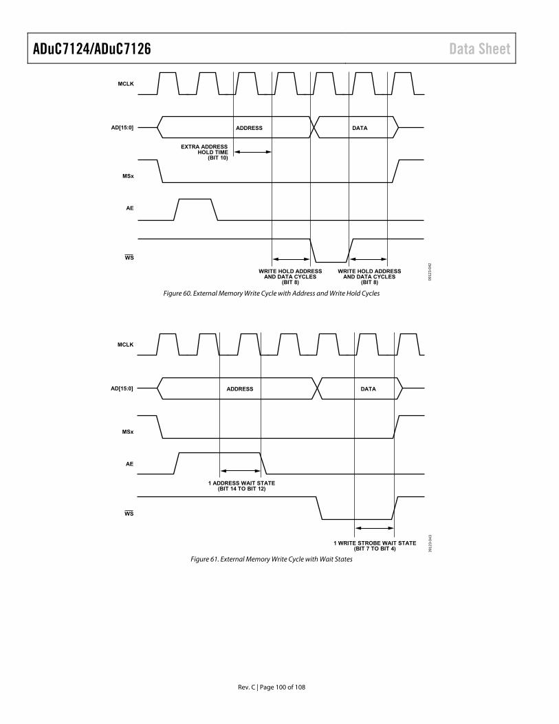
ADuC7124/ADuC7126 Data Sheet
Rev. C | Page 100 of 108
0912
3-04
2
DATAADDRESS
EXTRA ADDRESSHOLD TIME
(BIT 10)
WRITE HOLD ADDRESSAND DATA CYCLES
(BIT 8)
WRITE HOLD ADDRESSAND DATA CYCLES
(BIT 8)
MCLK
AD[15:0]
MSx
AE
WS
Figure 60. External Memory Write Cycle with Address and Write Hold Cycles
0912
3-04
3
DATAADDRESS
1 WRITE STROBE WAIT STATE(BIT 7 TO BIT 4)
1 ADDRESS WAIT STATE(BIT 14 TO BIT 12)
MCLK
AD[15:0]
MSx
AE
WS
Figure 61. External Memory Write Cycle with Wait States

Data Sheet ADuC7124/ADuC7126
Rev. C | Page 101 of 108
HARDWARE DESIGN CONSIDERATIONSPOWER SUPPLIES The ADuC7124/ADuC7126 operational power supply voltage range is 2.7 V to 3.6 V. Separate analog and digital power supply pins (AVDD and IOVDD, respectively) allow AVDD to be kept relatively free of noisy digital signals often present on the system IOVDD line. In this mode, the part can also operate with split supplies; that is, it can use different voltage levels for each supply. For example, the system can be designed to operate with an IOVDD voltage level of 3.3 V while the AVDD level can be at 3 V or vice versa. A typical split supply configuration is shown in Figure 62.
0912
3-04
4ADuC7124/ADuC7126
0.1µF
ANALOGSUPPLY
10µF
AVDD
DACVDD
GNDREF
DACGND
AGND
IOVDD
IOGND
0.1µF
+–
DIGITALSUPPLY
10µF+–
Figure 62. External Dual Supply Connections
As an alternative to providing two separate power supplies, the user can reduce noise on AVDD by placing a small series resistor and/or ferrite bead between AVDD and IOVDD and then decoupling AVDD separately to ground. An example of this configuration is shown in Figure 63. With this configuration, other analog circuitry (such as op amps, voltage reference, or any other analog circuitry) can be powered from the AVDD supply line as well.
0912
3-14
5
ADuC7124/ADuC7126
0.1µF
BEAD
AVDD
AGND
IOVDD
IOVDD
IOVDD
DGND
DGND
DGND
0.1µF
DIGITAL SUPPLY ANALOG SUPPLY
10µF 10µF+–
Figure 63. External Single Supply Connections
Notice that in both Figure 62 and Figure 63, a large value (10 μF) reservoir capacitor sits on IOVDD, and a separate 10 μF capacitor sits on AVDD. In addition, local small-value (0.1 μF) capacitors are located at each AVDD and IOVDD pin of the chip. As per standard design practice, be sure to include all of these capacitors and ensure that the smaller capacitors are close to each AVDD pin with trace lengths as short as possible. Connect the ground terminal of each of these capacitors directly to the underlying ground plane.
Finally, note that the analog and digital ground pins on the ADuC7124/ADuC7126 must be referenced to the same system ground reference point at all times.
IOVDD Supply Sensitivity
The IOVDD supply is sensitive to high frequency noise because it is the supply source for the internal oscillator and PLL circuits. When the internal PLL loses lock, the clock source is removed by a gating circuit from the CPU, and the ARM7TDMI core stops executing code until the PLL regains lock. This feature ensures that no flash interface timings or ARM7TDMI timings are violated.
Typically, frequency noise greater than 50 kHz and 50 mV p-p on top of the supply causes the core to stop working.
If decoupling values recommended in the Power Supplies section do not sufficiently dampen all noise sources below 50 mV on IOVDD, a filter such as the one shown in Figure 64 is recommended.
ADuC7124/ADuC7126
IOVDD
IOGND
0.1µF 0.1µF
DIGITALSUPPLY
10µF+–
1µH
0912
3-08
7
Figure 64. Recommended IOVDD Supply Filter
Linear Voltage Regulator
The ADuC7124/ADuC7126 require a single 3.3 V supply, but the core logic requires a 2.6 V supply. An on-chip linear regulator generates the 2.6 V from IOVDD for the core logic. The LVDD pin is the 2.6 V supply for the core logic. An external compensation capacitor of 0.47 μF must be connected between LVDD and DGND (as close as possible to these pins) to act as a tank of charge as shown in Figure 65.
0912
3-04
6
ADuC7124/ADuC7126
0.47µFLVDD
DGND
Figure 65. Voltage Regulator Connections
The LVDD pin should not be used for any other chip. It is also recommended to use excellent power supply decoupling on IOVDD to help improve line regulation performance of the on-chip voltage regulator.
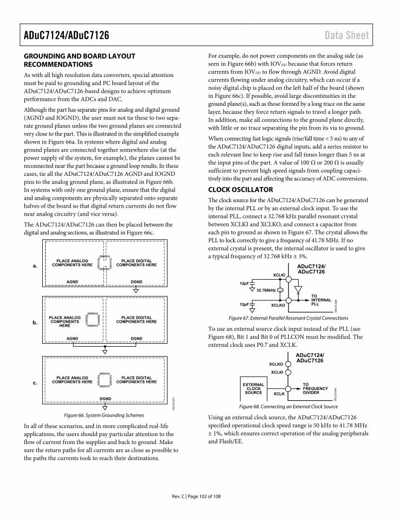
ADuC7124/ADuC7126 Data Sheet
Rev. C | Page 102 of 108
GROUNDING AND BOARD LAYOUT RECOMMENDATIONS As with all high resolution data converters, special attention must be paid to grounding and PC board layout of the ADuC7124/ADuC7126-based designs to achieve optimum performance from the ADCs and DAC.
Although the part has separate pins for analog and digital ground (AGND and IOGND), the user must not tie these to two sepa-rate ground planes unless the two ground planes are connected very close to the part. This is illustrated in the simplified example shown in Figure 66a. In systems where digital and analog ground planes are connected together somewhere else (at the power supply of the system, for example), the planes cannot be reconnected near the part because a ground loop results. In these cases, tie all the ADuC7124/ADuC7126 AGND and IOGND pins to the analog ground plane, as illustrated in Figure 66b. In systems with only one ground plane, ensure that the digital and analog components are physically separated onto separate halves of the board so that digital return currents do not flow near analog circuitry (and vice versa).
The ADuC7124/ADuC7126 can then be placed between the digital and analog sections, as illustrated in Figure 66c.
0912
3-04
7
a.PLACE ANALOG
COMPONENTS HEREPLACE DIGITAL
COMPONENTS HERE
AGND DGND
b.PLACE ANALOGCOMPONENTS
HERE
PLACE DIGITALCOMPONENTS HERE
AGND DGND
c.PLACE ANALOG
COMPONENTS HEREPLACE DIGITAL
COMPONENTS HERE
DGND
Figure 66. System Grounding Schemes
In all of these scenarios, and in more complicated real-life applications, the users should pay particular attention to the flow of current from the supplies and back to ground. Make sure the return paths for all currents are as close as possible to the paths the currents took to reach their destinations.
For example, do not power components on the analog side (as seen in Figure 66b) with IOVDD because that forces return currents from IOVDD to flow through AGND. Avoid digital currents flowing under analog circuitry, which can occur if a noisy digital chip is placed on the left half of the board (shown in Figure 66c). If possible, avoid large discontinuities in the ground plane(s), such as those formed by a long trace on the same layer, because they force return signals to travel a longer path. In addition, make all connections to the ground plane directly, with little or no trace separating the pin from its via to ground.
When connecting fast logic signals (rise/fall time < 5 ns) to any of the ADuC7124/ADuC7126 digital inputs, add a series resistor to each relevant line to keep rise and fall times longer than 5 ns at the input pins of the part. A value of 100 Ω or 200 Ω is usually sufficient to prevent high speed signals from coupling capaci-tively into the part and affecting the accuracy of ADC conversions.
CLOCK OSCILLATOR The clock source for the ADuC7124/ADuC7126 can be generated by the internal PLL or by an external clock input. To use the internal PLL, connect a 32.768 kHz parallel resonant crystal between XCLKI and XCLKO, and connect a capacitor from each pin to ground as shown in Figure 67. The crystal allows the PLL to lock correctly to give a frequency of 41.78 MHz. If no external crystal is present, the internal oscillator is used to give a typical frequency of 32.768 kHz ± 3%.
0912
3-04
8
ADuC7124/ADuC7126
TOINTERNALPLL
12pF
XCLKI
32.768kHz
12pF XCLKO
Figure 67. External Parallel Resonant Crystal Connections
To use an external source clock input instead of the PLL (see Figure 68), Bit 1 and Bit 0 of PLLCON must be modified. The external clock uses P0.7 and XCLK.
0912
3-04
9
ADuC7124/ADuC7126
TOFREQUENCYDIVIDER
XCLKO
XCLKI
XCLK
EXTERNALCLOCK
SOURCE
Figure 68. Connecting an External Clock Source
Using an external clock source, the ADuC7124/ADuC7126 specified operational clock speed range is 50 kHz to 41.78 MHz ± 1%, which ensures correct operation of the analog peripherals and Flash/EE.

Data Sheet ADuC7124/ADuC7126
Rev. C | Page 103 of 108
0912
3-05
0
IOVDD
3.3V
2.6V2.41V TYP2.41V TYP
128ms TYP
LVDD
POR
MRST
0.12ms TYP
POWER-ON RESET OPERATION An internal power-on reset (POR) is implemented on the ADuC7124/ADuC7126. For LVDD below 2.40 V typical, the internal POR holds the part in reset. As LVDD rises above 2.41 V, an internal timer times out for typically 128 ms before the part is released from reset. The user must ensure that the power supply, IOVDD, reaches a stable 2.7 V minimum level by this time. Likewise, on power-down, the internal POR holds the part in reset until LVDD drops below 2.40 V. Figure 69 illustrates the operation of the internal POR in detail.
Figure 69. Internal Power-On Reset Operation

ADuC7124/ADuC7126 Data Sheet
Rev. C | Page 104 of 108
OUTLINE DIMENSIONS
*COMPLIANT TO JEDEC STANDARDS MO-220-VMMD-4 EXCEPT FOR EXPOSED PAD DIMENSION
0.25 MIN
164
1617
4948
3233
0.500.400.30
0.50BSC
0.20 REF
12° MAX 0.80 MAX0.65 TYP
1.000.850.80
7.50 REF
0.05 MAX0.02 NOM
0.60 MAX0.60
MAX
SEATINGPLANE
PIN 1INDICATOR
*4.854.70 SQ4.55
PIN 1INDICATOR
0.300.230.18
FOR PROPER CONNECTION OFTHE EXPOSED PAD, REFER TOTHE PIN CONFIGURATION ANDFUNCTION DESCRIPTIONSSECTION OF THIS DATA SHEET.
TOP VIEW
EXPOSEDPAD
BOTTOM VIEW
9.109.00 SQ8.90
8.858.75 SQ8.65
04-0
4-20
12-A
Figure 70. 64-Lead Frame Chip Scale Package [LFCSP_VQ]
9 mm x 9 mm Body, Very Thin Quad (CP-64-1)
Dimensions shown in millimeters
COMPLIANT TO JEDEC STANDARDS MS-026-BDD 0517
06-A
0.150.05
1.45 1.40 1.35
0.20 0.09
0.08COPLANARITY
VIEW AROTATED 90° CCW
SEATINGPLANE
7°3.5°0°
TOP VIEW(PINS DOWN)
1
2141
40
606180
20
0.50BSC
LEAD PITCH
0.270.220.17
1.60MAX
0.750.600.45
VIEW A
PIN 1
14.2014.00 SQ13.80
12.2012.00 SQ11.80
Figure 71. 80-Lead Low Profile Quad Flat Package [LQFP]
(ST-80-1) Dimensions shown in millimeters
Data Sheet ADuC7124/ADuC7126
Rev. C | Page 105 of 108
ORDERING GUIDE
Model1ADC Channels
DAC Channels Flash/RAM GPIO Downloader
Temperature Range
Package Description
Package Option
Ordering Quantity
ADuC7124BCPZ126 10 2 126 kB/32 kB 30 UART −40°C to +125°C 64-Lead LFCSP_VQ
CP-64-1 260
ADuC7124BCPZ126-RL 10 2 126 kB/32 kB 30 UART −40°C to +125°C 64-Lead LFCSP_VQ
CP-64-1 2500
ADuC7126BSTZ126 12 4 126 kB/32 kB 40 UART −40°C to +125°C 80-Lead LQFP ST-80-1 119 ADuC7126BSTZ126-RL 12 4 126 kB/32 kB 40 UART −40°C to +125°C 80-Lead LQFP ST-80-1 1000 ADuC7126BSTZ126I 12 4 126 kB/32 kB 40 I2C −40°C to +125°C 80-Lead LQFP ST-80-1 119 ADuC7126BSTZ126IRL 12 4 126 kB/32 kB 40 I2C −40°C to +125°C 80-Lead LQFP ST-80-1 1000 EVAL-ADuC7124QSPZ ADuC7124
QuickStart Development System
EVAL-ADuC7126QSPZ ADuC7126 QuickStart Development System
1 Z = RoHS Compliant Part.

ADuC7124/ADuC7126 Data Sheet
Rev. C | Page 106 of 108
NOTES

Data Sheet ADuC7124/ADuC7126
Rev. C | Page 107 of 108
NOTES
ADuC7124/ADuC7126 Data Sheet
Rev. C | Page 108 of 108
NOTES
I2C refers to a communications protocol originally developed by Philips Semiconductors (now NXP Semiconductors).
©2010–2012 Analog Devices, Inc. All rights reserved. Trademarks and registered trademarks are the property of their respective owners. D09123-0-5/12(C)