DLP4710 0.47 1080p DMD. datasheet (Rev. A) · 2018-04-12 · Absolute Temperature delta between any...
42
Product Folder Sample & Buy Technical Documents Tools & Software Support & Community DLP4710 ZHCSDY1A – NOVEMBER 2014 – REVISED MAY 2015 DLP4710 0.47 1080p DMD 1 特性 3 说明 1• 0.47 英寸 (11.93mm) 对角线微镜阵列 DLP4710 数字微镜器件 (DMD) 是一款数控微光机电 系统 (MOEMS) 空间照明调制器 (SLM)。 当与适当的 – 1920 × 1080 铝制微米级微镜阵列,正交布局 光学系统耦合时,DLP4710 DMD 可显示非常清晰的 – 5.4 – 微米微镜间距 高质量图像或视频。 DLP4710 是 DLP4710 DMD、 – ±17° 微镜倾斜度(相对于平面) DLPC3439 显示控制器和 DLPA3000/DLPA3005 – 底部照明,实现最优的效率和光学引擎尺寸 PMIC/LED 驱动器所组成的芯片组的一部分。 – 偏振无关型铝微镜表面 DLP4710 紧凑的物理尺寸连同控制器和 PMIC/LED 驱 • 32 位 SubLVDS 输入数据总线 动器共同组成了完整的系统解决方案,从而实现了小外 • 专用 DLPC3439 显示控制器和 形尺寸、低功耗以及高分辨率 HD 显示。 DLPA3000/DLPA3005 电源管理集成电路 (PMIC)/ 发光二极管 (LED) 驱动器,确保可靠运行 器件信息 (1) 器件型号 封装 封装尺寸(标称值) 2 应用 DLP4710 CLGA (100) 24.50mm × 11mm × 3.80mm • 智能全高清 (HD) 投影仪 (1) 要了解所有可用封装,请见数据表末尾的可订购产品附录。 • 移动式附件全 HD 投影仪 • 无屏幕显示器 • 交互式显示屏 • 低延迟游戏显示屏 • 头戴式显示器 DLP ® DLP4710 0.47 1080p 芯片组 1 An IMPORTANT NOTICE at the end of this data sheet addresses availability, warranty, changes, use in safety-critical applications, intellectual property matters and other important disclaimers. PRODUCTION DATA. English Data Sheet: DLPS056
Transcript of DLP4710 0.47 1080p DMD. datasheet (Rev. A) · 2018-04-12 · Absolute Temperature delta between any...

Product
Folder
Sample &Buy
Technical
Documents
Tools &
Software
Support &Community
DLP4710ZHCSDY1A –NOVEMBER 2014–REVISED MAY 2015
DLP4710 0.47 1080p DMD1 特特性性 3 说说明明
1• 0.47 英寸 (11.93mm) 对角线微镜阵列 DLP4710 数字微镜器件 (DMD) 是一款数控微光机电
系统 (MOEMS) 空间照明调制器 (SLM)。 当与适当的– 1920 × 1080 铝制微米级微镜阵列,正交布局
光学系统耦合时,DLP4710 DMD 可显示非常清晰的– 5.4 – 微米微镜间距
高质量图像或视频。 DLP4710 是 DLP4710 DMD、– ±17° 微镜倾斜度(相对于平面)
DLPC3439 显示控制器和 DLPA3000/DLPA3005– 底部照明,实现最优的效率和光学引擎尺寸PMIC/LED 驱动器所组成的芯片组的一部分。– 偏振无关型铝微镜表面DLP4710 紧凑的物理尺寸连同控制器和 PMIC/LED 驱• 32 位 SubLVDS 输入数据总线动器共同组成了完整的系统解决方案,从而实现了小外• 专用 DLPC3439 显示控制器和形尺寸、低功耗以及高分辨率 HD 显示。DLPA3000/DLPA3005 电源管理集成电路 (PMIC)/
发光二极管 (LED) 驱动器,确保可靠运行器器件件信信息息(1)
器器件件型型号号 封封装装 封封装装尺尺寸寸((标标称称值值))2 应应用用DLP4710 CLGA (100) 24.50mm × 11mm × 3.80mm• 智能全高清 (HD) 投影仪(1) 要了解所有可用封装,请见数据表末尾的可订购产品附录。• 移动式附件全 HD 投影仪
• 无屏幕显示器
• 交互式显示屏
• 低延迟游戏显示屏
• 头戴式显示器
DLP® DLP4710 0.47 1080p 芯芯片片组组
1
An IMPORTANT NOTICE at the end of this data sheet addresses availability, warranty, changes, use in safety-critical applications,intellectual property matters and other important disclaimers. PRODUCTION DATA.
English Data Sheet: DLPS056

DLP4710ZHCSDY1A –NOVEMBER 2014–REVISED MAY 2015 www.ti.com.cn
目目录录
7.4 Device Functional Modes........................................ 221 特特性性.......................................................................... 17.5 Window Characteristics and Optics ........................ 222 应应用用.......................................................................... 17.6 Micromirror Array Temperature Calculation............ 233 说说明明.......................................................................... 17.7 Micromirror Landed-On/Landed-Off Duty Cycle .... 244 修修订订历历史史记记录录 ........................................................... 2
8 Application and Implementation ........................ 285 Pin Configuration and Functions ......................... 38.1 Application Information............................................ 286 Specifications......................................................... 88.2 Typical Application .................................................. 296.1 Absolute Maximum Ratings ..................................... 8
9 Power Supply Recommendations ...................... 316.2 Storage Conditions.................................................... 89.1 Power Supply Power-Up Procedure ...................... 316.3 ESD Ratings.............................................................. 99.2 Power Supply Power-Down Procedure .................. 316.4 Recommended Operating Conditions....................... 99.3 Power Supply Sequencing Requirements .............. 326.5 Thermal Information ................................................ 11
10 Layout................................................................... 346.6 Electrical Characteristics......................................... 1110.1 Layout Guidelines ................................................. 346.7 Timing Requirements .............................................. 1210.2 Layout Example .................................................... 346.8 Switching Characteristics ....................................... 17
11 器器件件和和文文档档支支持持 ..................................................... 356.9 System Mounting Interface Loads .......................... 1711.1 器件支持 ................................................................ 356.10 Physical Characteristics of the Micromirror Array. 1811.2 相关链接 ................................................................ 356.11 Micromirror Array Optical Characteristics ............. 1911.3 社区资源 ................................................................ 366.12 Window Characteristics......................................... 2011.4 商标 ....................................................................... 366.13 Chipset Component Usage Specification ............. 2011.5 静电放电警告......................................................... 367 Detailed Description ............................................ 2111.6 术语表 ................................................................... 367.1 Overview ................................................................. 21
12 机机械械、、封封装装和和可可订订购购信信息息....................................... 367.2 Functional Block Diagram ....................................... 217.3 Feature Description................................................. 22
4 修修订订历历史史记记录录
Changes from Original (November 2014) to Revision A Page
• 已将器件状态从产品预览更改为量产数据并已发布完整版文档............................................................................................... 1
2 Copyright © 2014–2015, Texas Instruments Incorporated

DLP4710www.ti.com.cn ZHCSDY1A –NOVEMBER 2014–REVISED MAY 2015
5 Pin Configuration and Functions
FQL Package100-Pin CLGABottom View
Pin Functions – Connector Pins (1)
PIN PACKAGE NETTYPE SIGNAL DATA RATE DESCRIPTION LENGTH (2) (mm)NAME NO.DATA INPUTSD_AN(0) G3 I SubLVDS Double Data, Negative 5.01D_AN(1) F4 I SubLVDS Double Data, Negative 2.03D_AN(2) E3 I SubLVDS Double Data, Negative 2.41D_AN(3) E6 I SubLVDS Double Data, Negative 4.71D_AN(4) J5 I SubLVDS Double Data, Negative 3.23D_AN(5) L5 I SubLVDS Double Data, Negative 3.87D_AN(6) G5 I SubLVDS Double Data, Negative 6.32D_AN(7) L3 I SubLVDS Double Data, Negative 1.84D_AP(0) H3 I SubLVDS Double Data, Positive 5.01D_AP(1) G4 I SubLVDS Double Data, Positive 2.03D_AP(2) E4 I SubLVDS Double Data, Positive 2.41D_AP(3) E5 I SubLVDS Double Data, Positive 4.71D_AP(4) J6 I SubLVDS Double Data, Positive 3.23
(1) Low speed interface is LPSDR and adheres to the Electrical Characteristics and AC/DC Operating Conditions table in JEDEC StandardNo. 209B, Low Power Double Data Rate (LPDDR) JESD209B.
(2) Net trace lengths inside the package:Relative dielectric constant for the FQL ceramic package is 9.8.Propagation speed = 11.8 / sqrt (9.8) = 3.769 inches/ns.Propagation delay = 0.265 ns/inch = 265 ps/inch = 10.43 ps/mm.
Copyright © 2014–2015, Texas Instruments Incorporated 3

DLP4710ZHCSDY1A –NOVEMBER 2014–REVISED MAY 2015 www.ti.com.cn
Pin Functions – Connector Pins(1) (continued)PIN PACKAGE NETTYPE SIGNAL DATA RATE DESCRIPTION LENGTH (2) (mm)NAME NO.
D_AP(5) L6 I SubLVDS Double Data, Positive 3.87D_AP(6) G6 I SubLVDS Double Data, Positive 6.32D_AP(7) L4 I SubLVDS Double Data, Positive 1.84D_BN(0) G27 I SubLVDS Double Data, Negative 2.51D_BN(1) E26 I SubLVDS Double Data, Negative 4.43D_BN(2) D28 I SubLVDS Double Data, Negative 2.76D_BN(3) D26 I SubLVDS Double Data, Negative 5.47D_BN(4) L25 I SubLVDS Double Data, Negative 4.85D_BN(5) K25 I SubLVDS Double Data, Negative 4.10D_BN(6) L28 I SubLVDS Double Data, Negative 2.53D_BN(7) K27 I SubLVDS Double Data, Negative 2.76D_BP(0) F27 I SubLVDS Double Data, Positive 2.51D_BP(1) E27 I SubLVDS Double Data, Positive 4.43D_BP(2) D27 I SubLVDS Double Data, Positive 2.76D_BP(3) D25 I SubLVDS Double Data, Positive 5.47D_BP(4) L26 I SubLVDS Double Data, Positive 4.85D_BP(5) J25 I SubLVDS Double Data, Positive 4.10D_BP(6) K28 I SubLVDS Double Data, Positive 2.53D_BP(7) J27 I SubLVDS Double Data, Positive 2.76DCLK_AN J3 I SubLVDS Double Clock, Negative 3.77DCLK_AP K3 I SubLVDS Double Clock, Positive 3.77DCLK_BN H26 I SubLVDS Double Clock, Negative 2.98DCLK_BP H27 I SubLVDS Double Clock, Positive 2.98CONTROL INPUTSLS_WDATA D3 I LPSDR (1) Single Write data for low speed interface. 1.20LS_CLK C3 I LPSDR Single Clock for low-speed interface 1.20
Asynchronous reset DMD signal. Alow signal places the DMD in reset. ADMD_DEN_ARSTZ B6 I LPSDR 4.19high signal releases the DMD fromreset and places it in active mode.
LS_RDATA_A C6 O LPSDR Single Read data for low-speed interface 3.93LS_RDATA_B C4 O LPSDR Single Read data for low-speed interface 2.57POWERVBIAS (3) B27 Power 24.51Supply voltage for positive bias level
at micromirrorsVBIAS (3) B4 Power 24.51VOFFSET (3) B2 Power Supply voltage for HVCMOS core 49.56
logic. Supply voltage for stepped highlevel at micromirror addresselectrodes.VOFFSET (3) C29 Power 49.56Supply voltage for offset level atmicromirrors.
VRESET B28 Power 24.82Supply voltage for negative reset levelat micromirrors.VRESET B3 Power 24.82
(3) The following power supplies are all required to operate the DMD: VDD, VDDI, VOFFSET, VBIAS, VRESET. All VSS connections arealso required.
4 Copyright © 2014–2015, Texas Instruments Incorporated

DLP4710www.ti.com.cn ZHCSDY1A –NOVEMBER 2014–REVISED MAY 2015
Pin Functions – Connector Pins(1) (continued)PIN PACKAGE NETTYPE SIGNAL DATA RATE DESCRIPTION LENGTH (2) (mm)NAME NO.
VDD (3) C2 PowerVDD D2 PowerVDD D29 PowerVDD E2 PowerVDD E29 PowerVDD H2 Power
Supply voltage for LVCMOS coreVDD H28 Power logic. Supply voltage for LPSDRVDD H29 Power inputs.
Supply voltage for normal high level atVDD J2 Power micromirror address electrodes.VDD J28 PowerVDD J29 PowerVDD K2 PowerVDD K29 PowerVDD L2 PowerVDD L29 PowerVDDI E28 PowerVDDI F2 PowerVDDI F28 PowerVDDI F29 Power Supply voltage for SubLVDS
receivers.VDDI F3 PowerVDDI G2 PowerVDDI G28 PowerVDDI G29 Power
Copyright © 2014–2015, Texas Instruments Incorporated 5

DLP4710ZHCSDY1A –NOVEMBER 2014–REVISED MAY 2015 www.ti.com.cn
Pin Functions – Connector Pins(1) (continued)PIN PACKAGE NETTYPE SIGNAL DATA RATE DESCRIPTION LENGTH (2) (mm)NAME NO.
VSS B25 GroundVSS B26 GroundVSS B29 GroundVSS B5 GroundVSS C25 GroundVSS C26 GroundVSS C27 GroundVSS C28 GroundVSS C5 GroundVSS D4 GroundVSS D5 GroundVSS D6 GroundVSS E25 GroundVSS F25 GroundVSS F26 Ground Common return.
Ground for all power.VSS F5 GroundVSS F6 GroundVSS G25 GroundVSS G26 GroundVSS H25 GroundVSS H4 GroundVSS H5 GroundVSS H6 GroundVSS J26 GroundVSS J4 GroundVSS K26 GroundVSS K4 GroundVSS K5 GroundVSS K6 GroundVSS L27 Ground
6 Copyright © 2014–2015, Texas Instruments Incorporated

DLP4710www.ti.com.cn ZHCSDY1A –NOVEMBER 2014–REVISED MAY 2015
Pin Functions – Test PadsNUMBER SYSTEM BOARD
A1 Do not connectA5 Do not connectA6 Do not connectA25 Do not connectA26 Do not connectA27 Do not connectA28 Do not connectA29 Do not connectA30 Do not connectA31 Do not connectB30 Do not connectB31 Do not connectC30 Do not connectC31 Do not connectD1 Do not connectE1 Do not connect
Copyright © 2014–2015, Texas Instruments Incorporated 7

DLP4710ZHCSDY1A –NOVEMBER 2014–REVISED MAY 2015 www.ti.com.cn
6 Specifications
6.1 Absolute Maximum Ratingssee (1)
MIN MAX UNITSupply voltage for LVCMOS core logic (2)
VDD –0.5 2.3 VSupply voltage for LPSDR low speed interfaceVDDI Supply voltage for SubLVDS receivers (2) –0.5 2.3 V
Supply voltage for HVCMOS and micromirrorVOFFSET –0.5 11 Velectrode (2) (3)
Supply voltage VBIAS Supply voltage for micromirror electrode (2) –0.5 19 VVRESET Supply voltage for micromirror electrode (2) –15 0.3 V| VDDI–VDD | Supply voltage delta (absolute value) (4) 0.3 V| VBIAS–VOFFSET | Supply voltage delta (absolute value) (5) 11 V| VBIAS–VRESET | Supply voltage delta (absolute value) (6) 34 VInput voltage for other inputs LPSDR (2) –0.5 VDD + 0.5 V
Input voltageInput voltage for other inputs SubLVDS (2) (7) –0.5 VDDI + 0.5 V| VID | SubLVDS input differential voltage (absolute value) (7) 810 mV
Input pinsIID SubLVDS input differential current 10 mAƒclock Clock frequency for low speed interface LS_CLK 130 MHzClock
frequency ƒclock Clock frequency for high speed interface DCLK 620 MHzTemperature – operational (8) –20 90 °C
TARRAY and TWINDOW Temperature – non-operational (8) –40 90 °CEnvironmental TDP Dew Point - operating and non-operating 81 °C
Absolute Temperature delta between any point on the|TDELTA| 30 °Cwindow edge and the ceramic test point TP1 (9)
(1) Stresses beyond those listed under Absolute Maximum Ratings may cause permanent damage to the device. These are stress ratingsonly, and functional operation of the device is not implied at these or any other conditions beyond those indicated under RecommendedOperating Conditions. Exposure above or below the Recommended Operating Conditions for extended periods may affect devicereliability.
(2) All voltage values are with respect to the ground terminals (VSS). The following power supplies are all required to operate the DMD:VDD, VDDI, VOFFSET, VBIAS, and VRESET. All VSS connections are also required.
(3) VOFFSET supply transients must fall within specified voltages.(4) Exceeding the recommended allowable absolute voltage difference between VDDI and VDD may result in excessive current draw.(5) Exceeding the recommended allowable absolute voltage difference between VBIAS and VOFFSET may result in excessive current
draw.(6) Exceeding the recommended allowable absolute voltage difference between VBIAS and VRESET may result in excessive current draw.(7) This maximum input voltage rating applies when each input of a differential pair is at the same voltage potential. Sub-LVDS differential
inputs must not exceed the specified limit or damage may result to the internal termination resistors.(8) The highest temperature of the active array (as calculated by the Micromirror Array Temperature Calculation) or of any point along the
Window Edge as defined in Figure 18. The locations of thermal test points TP2, TP3, TP4, and TP5 in Figure 18 are intended tomeasure the highest window edge temperature. If a particular application causes another point on the window edge to be at a highertemperature, that point should be used.
(9) Temperature delta is the highest difference between the ceramic test point 1 (TP1) and anywhere on the window edge as shown inFigure 18. The window test points TP2, TP3, TP4, and TP5 shown in Figure 18 are intended to result in the worst case delta. If aparticular application causes another point on the window edge to result in a larger delta temperature, that point should be used.
6.2 Storage Conditionsapplicable before the DMD is installed in the final product
MIN MAX UNITTstg DMD storage temperature -40 85 °C
Long-term (1) 24TDP Storage dew point °C
Short-term (2) 28
(1) Long-term is defined as the usable life of the device.(2) Dew points beyond the specified long-term dew point are for short-term conditions only, where short-term is defined as less than 60
cumulative days over the usable life of the device (operating, non-operating, or storage).
8 Copyright © 2014–2015, Texas Instruments Incorporated
DLP4710www.ti.com.cn ZHCSDY1A –NOVEMBER 2014–REVISED MAY 2015
6.3 ESD RatingsVALUE UNIT
Electrostatic Human body model (HBM), per ANSI/ESDA/JEDEC JS-001 (1)V(ESD) ±2000 Vdischarge
(1) JEDEC document JEP155 states that 500 V HBM allows safe manufacturing with a standard ESD control process.
6.4 Recommended Operating ConditionsOver operating free-air temperature range (unless otherwise noted) (1) (2) (3)
MIN NOM MAX UNITSUPPLY VOLTAGE RANGE (4)
VDD Supply voltage for LVCMOS core logic 1.7 1.8 1.95 VSupply voltage for LPSDR low-speed interface
VDDI Supply voltage for SubLVDS receivers 1.7 1.8 1.95 VVOFFSET Supply voltage for HVCMOS and micromirror 9.5 10 10.5 V
electrode (5)
VBIAS Supply voltage for mirror electrode 17.5 18 18.5 VVRESET Supply voltage for micromirror electrode –14.5 –14 –13.5 V|VDDI–VDD| Supply voltage delta (absolute value) (6) 0.3 V|VBIAS–VOFFSET| Supply voltage delta (absolute value) (7) 10.5 V|VBIAS–VRESET| Supply voltage delta (absolute value) (8) 33 VCLOCK FREQUENCYƒclock Clock frequency for low speed interface LS_CLK (9) 108 120 MHzƒclock Clock frequency for high speed interface DCLK (10) 300 540 MHz
Duty cycle distortion DCLK 44% 56%SUBLVDS INTERFACE (10)
| VID | SubLVDS input differential voltage (absolute value) 150 250 350 mVFigure 8 , Figure 9
VCM Common mode voltage Figure 8 , Figure 9 700 900 1100 mVVSUBLVDS SubLVDS voltage Figure 8, Figure 9 575 1225 mVZLINE Line differential impedance (PWB/trace) 90 100 110 ΩZIN Internal differential termination resistance Figure 10 80 100 120 Ω
100-Ω differential PCB trace 6.35 152.4 mm
(1) The following power supplies are all required to operate the DMD: VDD, VDDI, VOFFSET, VBIAS, and VRESET. All VSS connectionsare also required.
(2) Recommended Operating Conditions are applicable after the DMD is installed in the final product.(3) The functional performance of the device specified in this data sheet is achieved when operating the device within the limits defined by
the Recommended Operating Conditions. No level of performance is implied when operating the device above or below theRecommended Operating Conditions limits.
(4) All voltage values are with respect to the ground pins (VSS).(5) VOFFSET supply transients must fall within specified max voltages.(6) To prevent excess current, the supply voltage delta |VDDI – VDD| must be less than specified limit.(7) To prevent excess current, the supply voltage delta |VBIAS – VOFFSET| must be less than specified limit.(8) To prevent excess current, the supply voltage delta |VBIAS – VRESET| must be less than specified limit.(9) LS_CLK must run as specified to ensure internal DMD timing for reset waveform commands.(10) Refer to the SubLVDS timing requirements in Timing Requirements.
Copyright © 2014–2015, Texas Instruments Incorporated 9

Micromirror Landed Duty Cycle
Ope
ration
al (°
C)
0/100 5/95 10/90 15/85 20/80 25/75 30/70 35/65 40/60 45/5530
40
50
60
70
80
D001
50/50100/0 95/5 90/10 85/15 80/20 75/25 70/30 65/35 60/40 55/45
Max R
ecom
me
nd
ed
Arr
ay
Tem
pe
ratu
re–
DLP4710ZHCSDY1A –NOVEMBER 2014–REVISED MAY 2015 www.ti.com.cn
Recommended Operating Conditions (continued)Over operating free-air temperature range (unless otherwise noted)(1) (2) (3)
MIN NOM MAX UNITENVIRONMENTALTARRAY Array Temperature – long-term operational (11) (12) (13) 0 40 to 70 (13) °C
(14)
Array Temperature – short-term operational (12) (15) –20 75TDP Dew Point - long-term average (operational and non- 24 °C
operational) (14)
Dew Point - short-term (operational and non- 28 °Coperational) (16)
|TDELTA| Absolute Temperature difference between any point 30 °Con the window edge and the ceramic test point TP1 (17)
TWINDOW Window Temperature – operational (11) (18) 90 °CILLUV Illumination wavelengths < 400 nm (11) 0.68 mW/cm2
ILLVIS Illumination wavelengths between 400 nm and 700 nm Thermally limitedILLIR Illumination wavelengths > 700 nm 10 mW/cm2
(11) Simultaneous exposure of the DMD to the maximum Recommended Operating Conditions for temperature and UV illumination willreduce device lifetime.
(12) The array temperature cannot be measured directly and must be computed analytically from the temperature measured at test point 1(TP1) shown in Figure 18 and the package thermal resistance using Micromirror Array Temperature Calculation.
(13) Per Figure 1, the maximum operational array temperature should be derated based on the micromirror landed duty cycle that the DMDexperiences in the end application. Refer to Micromirror Landed-On/Landed-Off Duty Cycle for a definition of micromirror landed dutycycle.
(14) Long-term is defined as the usable life of the device.(15) Array temperatures beyond those specified as long-term are recommended for short-term conditions only (power-up). Short-term is
defined as cumulative time over the usable life of the device and is less than 500 hours for temperatures between the long-termmaximum and 75ºC, less than 500 hours for temperatures between 0ºC and –10ºC, and less than 25 hours for temperatures between -10ºC and -20ºC.
(16) Dew points beyond the specified long-term dew point are for short-term conditions only, where short-term is defined as less than 60cumulative days over the usable life of the device (operating, non-operating, or storage).
(17) Temperature delta is the highest difference between the ceramic test point 1 (TP1) and anywhere on the window edge shown inFigure 18. The window test points TP2, TP3, TP4, and TP5 shown in Figure 18 are intended to result in the worst case deltatemperature. If a particular application causes another point on the window edge to result in a larger delta temperature, that point shouldbe used.
(18) Window temperature is the highest temperature on the window edge shown in Figure 18. The locations of thermal test points TP2, TP3,TP4, and TP5 in Figure 18 are intended to measure the highest window edge temperature. If a particular application causes anotherpoint on the window edge to be at a higher temperature, that point should be used.
SPACE
Figure 1. Max Recommended Array Temperature – Derating Curve
10 Copyright © 2014–2015, Texas Instruments Incorporated

DLP4710www.ti.com.cn ZHCSDY1A –NOVEMBER 2014–REVISED MAY 2015
6.5 Thermal InformationFQL (LGA)
THERMAL METRIC (1) 100 PINS UNITMIN TYP MAX
Thermal resistance Active area to test point 1 (TP1) (1) 1.1 °C/W
(1) The DMD is designed to conduct absorbed and dissipated heat to the back of the package. The cooling system must be capable ofmaintaining the package within the temperature range specified in the Recommended Operating Conditions. The total heat load on theDMD is largely driven by the incident light absorbed by the active area; although other contributions include light energy absorbed by thewindow aperture and electrical power dissipation of the array. Optical systems should be designed to minimize the light energy fallingoutside the window clear aperture since any additional thermal load in this area can significantly degrade the reliability of the device.
6.6 Electrical CharacteristicsOver operating free-air temperature range (unless otherwise noted) (1)
PARAMETER TEST CONDITIONS (2) MIN TYP MAX UNITCURRENT
VDD = 1.95 V 260IDD Supply current: VDD (3) (4) mA
VDD = 1.8 V 180VDDI = 1.95 V 62
IDDI Supply current: VDDI (3) (4) mAVDD = 1.8 V 40VOFFSET = 10.5 V 7.4
IOFFSET Supply current: VOFFSET (5) (6) mAVOFFSET = 10 V 6.3VBIAS = 18.5 V 1.1
IBIAS Supply current: VBIAS (5) (6) mAVBIAS = 18 V 0.9VRESET = –14.5 V 5.4
IRESET Supply current: VRESET (6) mAVRESET = –14 V 4.4
POWER (7)
VDD = 1.95 V 507PDD Supply power dissipation: VDD (3) (4) mW
VDD = 1.8 V 324VDDI = 1.95 V 120.9
PDDI Supply power dissipation: VDDI (3) (4) mWVDD = 1.8 V 72VOFFSET = 10.5 V 77.7Supply power dissipation:POFFSET mWVOFFSET (5) (6) VOFFSET = 10 V 63VBIAS = 18.5 V 20.35
PBIAS Supply power dissipation: VBIAS (5) (6) mWVBIAS = 18 V 16.2VRESET = –14.5 V 78.3
PRESET Supply power dissipation: VRESET (6) mWVRESET = –14 V 61.6
PTOTAL Supply power dissipation: Total 536.8 804.25 mWLPSDR INPUT (8)
VIH(DC) DC input high voltage (9) 0.7 × VDD VDD + 0.3 VVIL(DC) DC input low voltage (9) –0.3 0.3 × VDD VVIH(AC) AC input high voltage (9) 0.8 × VDD VDD + 0.3 VVIL(AC) AC input low voltage (9) –0.3 0.2 × VDD V∆VT Hysteresis ( VT+ – VT– ) Figure 10 0.1 × VDD 0.4 × VDD V
(1) Device electrical characteristics are over Recommended Operating Conditions unless otherwise noted.(2) All voltage values are with respect to the ground pins (VSS).(3) To prevent excess current, the supply voltage delta |VDDI – VDD| must be less than specified limit.(4) Supply power dissipation based on non–compressed commands and data.(5) To prevent excess current, the supply voltage delta |VBIAS – VOFFSET| must be less than specified limit.(6) Supply power dissipation based on 3 global resets in 200 µs.(7) The following power supplies are all required to operate the DMD: VDD, VDDI, VOFFSET, VBIAS, VRESET. All VSS connections are
also required.(8) LPSDR specifications are for pins LS_CLK and LS_WDATA.(9) Low-speed interface is LPSDR and adheres to the Electrical Characteristics and AC/DC Operating Conditions table in JEDEC Standard
No. 209B, Low-Power Double Data Rate (LPDDR) JESD209B.
Copyright © 2014–2015, Texas Instruments Incorporated 11

DLP4710ZHCSDY1A –NOVEMBER 2014–REVISED MAY 2015 www.ti.com.cn
Electrical Characteristics (continued)Over operating free-air temperature range (unless otherwise noted)(1)
PARAMETER TEST CONDITIONS (2) MIN TYP MAX UNITIIL Low–level input current VDD = 1.95 V; VI = 0 V –100 nAIIH High–level input current VDD = 1.95 V; VI = 1.95 V 100 nALPSDR OUTPUT (10)
VOH DC output high voltage IOH = –2 mA 0.8 × VDD VVOL DC output low voltage IOL = 2 mA 0.2 × VDD VCAPACITANCE
Input capacitance LPSDR ƒ = 1 MHz 10 pFCIN Input capacitance SubLVDS ƒ = 1 MHz 20 pFCOUT Output capacitance ƒ = 1 MHz 10 pFCRESET Reset group capacitance ƒ = 1 MHz; (1080 × 240) micromirrors 400 450 pF
(10) LPSDR specification is for pin LS_RDATA.
6.7 Timing RequirementsDevice electrical characteristics are over Recommended Operating Conditions unless otherwise noted.
MIN NOM MAX UNITLPSDRtr Rise slew rate (1) (30% to 80%) × VDD, Figure 3 1 3 V/nstƒ Fall slew rate (1) (70% to 20%) × VDD, Figure 3 1 3 V/nstr Rise slew rate (2) (20% to 80%) × VDD, Figure 3 0.25 V/nstƒ Fall slew rate (2) (80% to 20%) × VDD, Figure 3 0.25 V/nstc Cycle time LS_CLK, Figure 2 7.7 8.3 nstW(H) Pulse duration LS_CLK 3.1 ns50% to 50% reference points, Figure 2hightW(L) Pulse duration LS_CLK 3.1 ns50% to 50% reference points, Figure 2lowtsu Setup time LS_WDATA valid before LS_CLK ↑, Figure 2 1.5 nst h Hold time LS_WDATA valid after LS_CLK ↑, Figure 2 1.5 nstWINDOW Window time (1) (3) Setup time + Hold time, Figure 2 3 ns
Window time derating (1) For each 0.25 V/ns reduction in slew rate below 0.35 nstDERATING (3) 1 V/ns, Figure 5SubLVDStr Rise slew rate 20% to 80% reference points, Figure 4 0.7 1 V/nstƒ Fall slew rate 80% to 20% reference points, Figure 4 0.7 1 V/nstc Cycle time DCLK, Figure 6 1.79 1.85 nstW(H) Pulse duration DCLK high 50% to 50% reference points, Figure 6 0.79 nstW(L) Pulse duration DCLK low 50% to 50% reference points, Figure 6 0.79 ns
D(0:7) valid beforetsu Setup time DCLK ↑ or DCLK ↓, Figure 6D(0:7) valid aftert h Hold time DCLK ↑ or DCLK ↓, Figure 6
tWINDOW Window time Setup time + Hold time, Figure 6, Figure 7 0.3 nstLVDS- Power-up receiver (4) 2000 nsENABLE+REFGEN
(1) Specification is for LS_CLK and LS_WDATA pins. Refer to LPSDR input rise slew rate and fall slew rate in Figure 3.(2) Specification is for DMD_DEN_ARSTZ pin. Refer to LPSDR input rise and fall slew rate in Figure 3.(3) Window time derating example: 0.5-V/ns slew rate increases the window time by 0.7 ns, from 3 to 3.7 ns.(4) Specification is for SubLVDS receiver time only and does not take into account commanding and latency after commanding.
12 Copyright © 2014–2015, Texas Instruments Incorporated

0.0 * VDD
0.2 * VDD0.3 * VDD
0.7 * VDD0.8 * VDD
1.0 * VDD
VIH(AC)
VIH(DC)
VIL(DC)
VIL(AC)
tftr
LS_CLK, LS_WDATA
0.0 * VDD
0.2 * VDD
0.8 * VDD
1.0 * VDD
tftr
DMD_DEN_ARSTZ
LS_WDATA
LS_CLK
tw(H) tw(L)
tc
50%50%50%
50% 50%
th
tsu
twindow
DLP4710www.ti.com.cn ZHCSDY1A –NOVEMBER 2014–REVISED MAY 2015
Low-speed interface is LPSDR and adheres to the Electrical Characteristics and AC/DC Operating Conditions table inJEDEC Standard No. 209B, Low Power Double Data Rate (LPDDR) JESD209B.
Figure 2. LPSDR Switching Parameters
Figure 3. LPSDR Input Rise and Fall Slew Rate
Figure 4. SubLVDS Input Rise and Fall Slew Rate
Copyright © 2014–2015, Texas Instruments Incorporated 13

LS_WDATA
LS_CLK
tSU tH
tWINDOW
VIH MIN
VIL MAX
Midpoint
VIH MIN
VIL MAX
Midpoint
tSU tH
tWINDOW
VIH MIN
VIL MAX
Midpoint
VIH MIN
VIL MAX
Midpoint
LS_WDATA
LS_CLK
tDERATING
DLP4710ZHCSDY1A –NOVEMBER 2014–REVISED MAY 2015 www.ti.com.cn
Figure 5. Window Time Derating Concept
Figure 6. SubLVDS Switching Parameters
14 Copyright © 2014–2015, Texas Instruments Incorporated

VCM VID
VSubLVDS max = VCM max + | 1/2 * VID max|
0.575V
1.225V
VSubLVDS min = VCM min – | 1/2 * VID max |
DLP4710www.ti.com.cn ZHCSDY1A –NOVEMBER 2014–REVISED MAY 2015
Note: Refer to High-Speed Interface for details.
Figure 7. High-Speed Training Scan Window
Figure 8. SubLVDS Voltage Parameters
Figure 9. SubLVDS Waveform Parameters
Copyright © 2014–2015, Texas Instruments Incorporated 15

CL
Tester ChannelOutput Under Test
Data Sheet Timing Reference Point
Device Pin
Stop Start
LS_CLK
LS_WDATA
LS_RDATA
Acknowledge
tPD
VIH
Δ VT
VT+
VT-VIL
LS_WDATA
LS_CLK
Not to Scale
DLP4710ZHCSDY1A –NOVEMBER 2014–REVISED MAY 2015 www.ti.com.cn
Figure 10. SubLVDS Equivalent Input Circuit
Figure 11. LPSDR Input Hysteresis
Figure 12. LPSDR Read Out
See Timing for more information.
Figure 13. Test Load Circuit for Output Propagation Measurement
16 Copyright © 2014–2015, Texas Instruments Incorporated

DLP4710www.ti.com.cn ZHCSDY1A –NOVEMBER 2014–REVISED MAY 2015
6.8 Switching Characteristics (1)
Over operating free-air temperature range (unless otherwise noted).PARAMETER TEST CONDITIONS MIN TYP MAX UNIT
CL = 5 pF 11.1 nsOutput propagation, Clock to Q, risingtPD edge of LS_CLK input to LS_RDATA CL = 10 pF 11.3 ns
output. Figure 12 CL = 85 pF 15 nsSlew rate, LS_RDATA 0.5 V/nsOutput duty cycle distortion, LS_RDATA 40% 60%
(1) Device electrical characteristics are over Recommended Operating Conditions unless otherwise noted.
6.9 System Mounting Interface Loads
PARAMETER MIN NOM MAX UNITMaximum system mounting interface load to be applied to the:
62 N• Thermal Interface Area (see Figure 14)110 N• Clamping and Electrical Interface Area (see Figure 14)
Figure 14. System Interface Loads
Copyright © 2014–2015, Texas Instruments Incorporated 17

ε
ε
εε
DLP4710ZHCSDY1A –NOVEMBER 2014–REVISED MAY 2015 www.ti.com.cn
6.10 Physical Characteristics of the Micromirror Array
PARAMETER VALUE UNITNumber of active columns See Figure 15 1920 micromirrorsNumber of active rows See Figure 15 1080 micromirrors
ε Micromirror (pixel) pitch See Figure 16 5.4 µmMicromirror active array Micromirror pitch × number of active columns; see Figure 15 10.368 mmwidthMicromirror active array Micromirror pitch × number of active rows; see Figure 15 5.832 mmheightMicromirror active border Pond of micromirror (POM) (1) 20 micromirrors/side
(1) The structure and qualities of the border around the active array includes a band of partially functional micromirrors called the POM.These micromirrors are structurally and/or electrically prevented from tilting toward the bright or ON state, but still require an electricalbias to tilt toward OFF.
Figure 15. Micromirror Array Physical Characteristics
Figure 16. Mirror (Pixel) Pitch
18 Copyright © 2014–2015, Texas Instruments Incorporated

DLP4710www.ti.com.cn ZHCSDY1A –NOVEMBER 2014–REVISED MAY 2015
6.11 Micromirror Array Optical Characteristics
PARAMETER TEST CONDITIONS MIN NOM MAX UNITMicromirror tilt angle DMD landed state (1) 17 °Micromirror tilt angle tolerance (2) (3) (4) (5) –1 1 °
Landed ON state 180Micromirror tilt direction (6) (7) °
Landed OFF state 270Micromirror crossover time Typical Performance 1.5 4
μsMicromirror switching time Typical Performance 6
Adjacent micromirrors 0Number of out-of-specification micromirrorsmicromirrors (8) Non-adjacent micromirrors 10
(1) Measured relative to the plane formed by the overall micromirror array.(2) Additional variation exists between the micromirror array and the package datums.(3) Represents the landed tilt angle variation relative to the nominal landed tilt angle.(4) Represents the variation that can occur between any two individual micromirrors, located on the same device or located on different
devices.(5) For some applications, it is critical to account for the micromirror tilt angle variation in the overall system optical design. With some
system optical designs, the micromirror tilt angle variation within a device may result in perceivable non-uniformities in the light fieldreflected from the micromirror array. With some system optical designs, the micromirror tilt angle variation between devices may result incolorimetry variations, system efficiency variations or system contrast variations.
(6) When the micromirror array is landed (not parked), the tilt direction of each individual micromirror is dictated by the binary contents ofthe CMOS memory cell associated with each individual micromirror. A binary value of 1 results in a micromirror landing in the ON Statedirection. A binary value of 0 results in a micromirror landing in the OFF State direction.
(7) Micromirror tilt direction is measured as in a typical polar coordinate system: measuring counter-clockwise from a 0° reference which isaligned with the +X Cartesian axis.
(8) An out-of-specification micromirror is defined as a micromirror that is unable to transition between the two landed states within thespecified Micromirror Switching Time.
Figure 17. Landed Pixel Orientation and Tilt
Copyright © 2014–2015, Texas Instruments Incorporated 19

DLP4710ZHCSDY1A –NOVEMBER 2014–REVISED MAY 2015 www.ti.com.cn
6.12 Window Characteristics
PARAMETER (1) MIN NOM MAX UNITWindow material designation Corning Eagle XGWindow refractive index at wavelength 546.1 nm 1.5119Window aperture (2) See (2)
Illumination overfill (3) See (3)
Window transmittance, single-pass Minimum within the wavelength range 97%through both surfaces and glass 420 to 680 nm. Applies to all angles 0°
to 30° AOI.Window Transmittance, single-pass Average over the wavelength range 420 97%through both surfaces and glass to 680 nm. Applies to all angles 30° to
45° AOI.
(1) See Window Characteristics and Optics for more information.(2) See the package mechanical characteristics for details regarding the size and location of the window aperture.(3) The active area of the DLP4710 device is surrounded by an aperture on the inside of the DMD window surface that masks structures of
the DMD device assembly from normal view. The aperture is sized to anticipate several optical conditions. Overfill light illuminating thearea outside the active array can scatter and create adverse effects to the performance of an end application using the DMD. Theillumination optical system should be designed to limit light flux incident outside the active array to less than 10% of the average fluxlevel in the active area. Depending on the particular system's optical architecture and assembly tolerances, the amount of overfill light onthe outside of the active array may cause system performance degradation.
SPACER
6.13 Chipset Component Usage SpecificationThe DLP4710 is a component of one or more DLP chipsets. Reliable function and operation of the DLP4710requires that it be used in conjunction with the other components of the applicable DLP chipset, including thosecomponents that contain or implement TI DMD control technology. TI DMD control technology is the TItechnology and devices for operating or controlling a DLP DMD.
NOTETI assumes no responsibility for image quality artifacts or DMD failures caused by opticalsystem operating conditions exceeding limits described previously
20 Copyright © 2014–2015, Texas Instruments Incorporated

DLP4710www.ti.com.cn ZHCSDY1A –NOVEMBER 2014–REVISED MAY 2015
7 Detailed Description
7.1 OverviewThe DLP4710 is a 0.47 inch diagonal spatial light modulator of aluminum micromirrors. Pixel array size is 1920columns by 1080 rows in a square grid pixel arrangement. The electrical interface is Sub Low Voltage DifferentialSignaling (SubLVDS) data.
DLP4710 is part of the chipset comprising of the DLP4710 DMD, DLPC3439 display controller andDLPA3000/DLPA3005 PMIC/LED driver. To ensure reliable operation, DLP4710 DMD must always be used withDLPC3439 display controller and DLPA3000/DLPA3005 PMIC/LED drivers.
7.2 Functional Block Diagram
(1) Details omitted for clarity.
Copyright © 2014–2015, Texas Instruments Incorporated 21

DLP4710ZHCSDY1A –NOVEMBER 2014–REVISED MAY 2015 www.ti.com.cn
7.3 Feature Description
7.3.1 Power InterfaceThe power management IC, DLPA3000/DLPA3005, contains 3 regulated DC supplies for the DMD reset circuitry:VBIAS, VRESET and VOFFSET, as well as the 2 regulated DC supplies for the DLPC3439 controller.
7.3.2 Low-Speed InterfaceThe Low Speed Interface handles instructions that configure the DMD and control reset operation. LS_CLK is thelow–speed clock, and LS_WDATA is the low speed data input.
7.3.3 High-Speed InterfaceThe purpose of the high-speed interface is to transfer pixel data rapidly and efficiently, making use of high speedDDR transfer and compression techniques to save power and time. The high-speed interface is composed ofdifferential SubLVDS receivers for inputs, with a dedicated clock.
7.3.4 TimingThe data sheet provides timing at the device pin. For output timing analysis, the tester pin electronics and itstransmission line effects must be taken into account. Figure 13 shows an equivalent test load circuit for theoutput under test. Timing reference loads are not intended as a precise representation of any particular systemenvironment or depiction of the actual load presented by a production test. System designers should use IBIS orother simulation tools to correlate the timing reference load to a system environment. The load capacitance valuestated is only for characterization and measurement of AC timing signals. This load capacitance value does notindicate the maximum load the device is capable of driving.
7.4 Device Functional ModesDMD functional modes are controlled by the DLPC3439 controller. See the DLPC3439 controller data sheet orcontact a TI applications engineer.
7.5 Window Characteristics and Optics
7.5.1 Optical Interface and System Image QualityTI assumes no responsibility for end-equipment optical performance. Achieving the desired end-equipmentoptical performance involves making trade-offs between numerous component and system design parameters.Optimizing system optical performance and image quality strongly relate to optical system design parametertrades. Although it is not possible to anticipate every conceivable application, projector image quality and opticalperformance is contingent on compliance to the optical system operating conditions described in the followingsections:
7.5.1.1 Numerical Aperture and Stray Light ControlThe angle defined by the numerical aperture of the illumination and projection optics at the DMD optical areashould be the same. This angle should not exceed the nominal device mirror tilt angle unless appropriateapertures are added in the illumination and/or projection pupils to block out flat-state and stray light from theprojection lens. The mirror tilt angle defines DMD capability to separate the ON optical path from any other lightpath, including undesirable flat–state specular reflections from the DMD window, DMD border structures, or othersystem surfaces near the DMD such as prism or lens surfaces. If the numerical aperture exceeds the mirror tiltangle, or if the projection numerical aperture angle is more than two degrees larger than the illuminationnumerical aperture angle, objectionable artifacts in the display’s border and/or active area could occur.
7.5.1.2 Pupil MatchTI’s optical and image quality specifications assume that the exit pupil of the illumination optics is nominallycentered within 2° of the entrance pupil of the projection optics. Misalignment of pupils can create objectionableartifacts in the display’s border and/or active area, which may require additional system apertures to control,especially if the numerical aperture of the system exceeds the pixel tilt angle.
22 Copyright © 2014–2015, Texas Instruments Incorporated

DLP4710www.ti.com.cn ZHCSDY1A –NOVEMBER 2014–REVISED MAY 2015
Window Characteristics and Optics (continued)7.5.1.3 Illumination OverfillThe active area of the device is surrounded by an aperture on the inside DMD window surface that masksstructures of the DMD chip assembly from normal view, and is sized to anticipate several optical operatingconditions. Overfill light illuminating the window aperture can create artifacts from the edge of the windowaperture opening and other surface anomalies that may be visible on the screen. The illumination optical systemshould be designed to limit light flux incident anywhere on the window aperture from exceeding approximately10% of the average flux level in the active area. Depending on the particular system’s optical architecture, overfilllight may have to be further reduced below the suggested 10% level in order to be acceptable.
7.6 Micromirror Array Temperature Calculation
Figure 18. DMD Thermal Test Points
Copyright © 2014–2015, Texas Instruments Incorporated 23

DLP4710ZHCSDY1A –NOVEMBER 2014–REVISED MAY 2015 www.ti.com.cn
Micromirror Array Temperature Calculation (continued)Micromirror array temperature can be computed analytically from measurement points on the outside of thepackage, the ceramic package thermal resistance, the electrical power dissipation, and the illumination heat load.The relationship between micromirror array temperature and the reference ceramic temperature is provided bythe following equations:
TARRAY = TCERAMIC + (QARRAY × RARRAY–TO–CERAMIC) (1)QARRAY = QELECTRICAL + QILLUMINATION (2)QILLUMINATION = (CL2W × SL)
• TARRAY = Computed DMD array temperature (°C)• TCERAMIC = Measured ceramic temperature (°C), TP1 location in Figure 18• RARRAY–TO–CERAMIC = DMD package thermal resistance from array to outside ceramic (°C/W) specified in
Thermal Information• QARRAY = Total DMD power; electrical, specified in Electrical Characteristics , plus absorbed (calculated) (W)• QELECTRICAL = Nominal DMD electrical power dissipation (W), specified in Electrical Characteristics• CL2W = Conversion constant for screen lumens to absorbed optical power on the DMD (W/lm) specified below• SL = Measured ANSI screen lumens (lm) (3)
Electrical power dissipation of the DMD is variable and depends on the voltages, data rates and operatingfrequencies. Refer to the specifications in Electrical Characteristics . Absorbed optical power from the illuminationsource is variable and depends on the operating state of the micromirrors and the intensity of the light source.Equations shown above are valid for a 1-chip DMD system with total projection efficiency through the projectionlens from DMD to the screen of 87%.
The conversion constant CL2W is based on the DMD micromirror array characteristics. It assumes a spectralefficiency of 300 lm/W for the projected light and illumination distribution of 83.7% on the DMD active array, and16.3% on the DMD array border and window aperture. The conversion constant is calculated to be 0.00266W/lm.
Sample Calculation for typical projection application:1. TCERAMIC = 55°C, assumed system measurement; see Recommended Operating Conditions for specification
limits.2. SL = 1500 lm3. QELECTRICAL = 1.1 W; See the table notes in Recommended Operating Conditions for details.4. CL2W = 0.00266 W/lm5. QARRAY = 0.25 + (0.00266 × 1500) = 4.24 W6. TARRAY = 55°C + (4.24 W × 1.1°C/W) = 59.66°C
7.7 Micromirror Landed-On/Landed-Off Duty Cycle
7.7.1 Definition of Micromirror Landed-On/Landed-Off Duty CycleThe micromirror landed-on/landed-off duty cycle (landed duty cycle) denotes the amount of time (as apercentage) that an individual micromirror is landed in the On state versus the amount of time the samemicromirror is landed in the Off state.
As an example, a landed duty cycle of 100/0 indicates that the referenced pixel is in the On state 100% of thetime (and in the Off state 0% of the time), whereas 0/100 would indicate that the pixel is in the Off state 100% ofthe time. Likewise, 50/50 indicates that the pixel is On 50% of the time and Off 50% of the time.
Note that when assessing landed duty cycle, the time spent switching from one state (ON or OFF) to the otherstate (OFF or ON) is considered negligible and is thus ignored.
Since a micromirror can only be landed in one state or the other (On or Off), the two numbers (percentages)always add to 100.
24 Copyright © 2014–2015, Texas Instruments Incorporated

DLP4710www.ti.com.cn ZHCSDY1A –NOVEMBER 2014–REVISED MAY 2015
Micromirror Landed-On/Landed-Off Duty Cycle (continued)7.7.2 Landed Duty Cycle and Useful Life of the DMDKnowing the long-term average landed duty cycle (of the end product or application) is important becausesubjecting all (or a portion) of the DMD’s micromirror array (also called the active array) to an asymmetric landedduty cycle for a prolonged period of time can reduce the DMD’s usable life.
Note that it is the symmetry/asymmetry of the landed duty cycle that is of relevance. The symmetry of the landedduty cycle is determined by how close the two numbers (percentages) are to being equal. For example, a landedduty cycle of 50/50 is perfectly symmetrical whereas a landed duty cycle of 100/0 or 0/100 is perfectlyasymmetrical.
7.7.3 Landed Duty Cycle and Operational DMD TemperatureOperational DMD Temperature and Landed Duty Cycle interact to affect the DMD’s usable life, and thisinteraction can be exploited to reduce the impact that an asymmetrical Landed Duty Cycle has on the DMD’susable life. This is quantified in the de-rating curve shown in Figure 1. The importance of this curve is that:• All points along this curve represent the same usable life.• All points above this curve represent lower usable life (and the further away from the curve, the lower the
usable life).• All points below this curve represent higher usable life (and the further away from the curve, the higher the
usable life).
In practice, this curve specifies the Maximum Operating DMD Temperature that the DMD should be operated atfor a given long-term average Landed Duty Cycle.
7.7.4 Estimating the Long-Term Average Landed Duty Cycle of a Product or ApplicationDuring a given period of time, the Landed Duty Cycle of a given pixel follows from the image content beingdisplayed by that pixel.
For example, in the simplest case, when displaying pure-white on a given pixel for a given time period, that pixelwill experience a 100/0 Landed Duty Cycle during that time period. Likewise, when displaying pure-black, thepixel will experience a 0/100 Landed Duty Cycle.
Between the two extremes (ignoring for the moment color and any image processing that may be applied to anincoming image), the Landed Duty Cycle tracks one-to-one with the gray scale value, as shown in Table 1.
Table 1. Grayscale Value andLanded Duty Cycle
Grayscale Landed Duty CycleValue0% 0/10010% 10/9020% 20/8030% 30/7040% 40/6050% 50/5060% 60/4070% 70/3080% 80/2090% 90/10100% 100/0
Accounting for color rendition (but still ignoring image processing) requires knowing both the color intensity (from0% to 100%) for each constituent primary color (red, green, and/or blue) for the given pixel as well as the colorcycle time for each primary color, where “color cycle time” is the total percentage of the frame time that a givenprimary must be displayed in order to achieve the desired white point.
During a given period of time, the landed duty cycle of a given pixel can be calculated as follows:
Copyright © 2014–2015, Texas Instruments Incorporated 25

DLP4710ZHCSDY1A –NOVEMBER 2014–REVISED MAY 2015 www.ti.com.cn
Landed Duty Cycle = (Red_Cycle_% × Red_Scale_Value) + (Green_Cycle_% × Green_Scale_Value) +(Blue_Cycle_%×Blue_Scale_Value)
whereRed_Cycle_%, Green_Cycle_%, and Blue_Cycle_%. represent the percentage of the frame time that Red, Green, andBlue are displayed (respectively) to achieve the desired white point. (4)
For example, assume that the red, green and blue color cycle times are 50%, 20%, and 30% respectively (inorder to achieve the desired white point), then the Landed Duty Cycle for various combinations of red, green,blue color intensities would be as shown in Table 2.
Table 2. Example Landed Duty Cycle for Full-ColorPixels
Red Cycle Green Cycle Blue CyclePercentage Percentage Percentage
50% 20% 30%
Red Scale Green Scale Blue Scale Landed DutyValue Value Value Cycle
0% 0% 0% 0/100100% 0% 0% 50/50
0% 100% 0% 20/800% 0% 100% 30/70
12% 0% 0% 6/940% 35% 0% 7/930% 0% 60% 18/82
100% 100% 0% 70/300% 100% 100% 50/50
100% 0% 100% 80/2012% 35% 0% 13/870% 35% 60% 25/75
12% 0% 60% 24/76100% 100% 100% 100/0
The last factor to account for in estimating the Landed Duty Cycle is any applied image processing. Within theDLP Controller DLPC3439, the two functions which affect Landed Duty Cycle are Gamma and IntelliBright™.
Gamma is a power function of the form Output_Level = A × Input_LevelGamma, where A is a scaling factor that istypically set to 1.
In the DLPC3430/DLPC3435 controller, gamma is applied to the incoming image data on a pixel-by-pixel basis.A typical gamma factor is 2.2, which transforms the incoming data as shown in Figure 19.
26 Copyright © 2014–2015, Texas Instruments Incorporated

Input Level (%)
Out
put L
evel
(%
)
0 10 20 30 40 50 60 70 80 90 1000
10
20
30
40
50
60
70
80
90
100
D002
Gamma = 2.2
DLP4710www.ti.com.cn ZHCSDY1A –NOVEMBER 2014–REVISED MAY 2015
Figure 19. Example of Gamma = 2.2
From Figure 19, if the gray scale value of a given input pixel is 40% (before gamma is applied), then gray scalevalue will be 13% after gamma is applied. Therefore, it can be seen that since gamma has a direct impactdisplayed gray scale level of a pixel, it also has a direct impact on the landed duty cycle of a pixel.
The IntelliBright algorithms content adaptive illumination control (CAIC) and local area brightness boost (LABB)also apply transform functions on the gray scale level of each pixel.
But while amount of gamma applied to every pixel (of every frame) is constant (the exponent, gamma, isconstant), CAIC and LABB are both adaptive functions that can apply a different amounts of either boost orcompression to every pixel of every frame.
Consideration must also be given to any image processing which occurs before the DLPC3439 controller.
Copyright © 2014–2015, Texas Instruments Incorporated 27

DLP4710ZHCSDY1A –NOVEMBER 2014–REVISED MAY 2015 www.ti.com.cn
8 Application and Implementation
NOTEInformation in the following applications sections is not part of the TI componentspecification, and TI does not warrant its accuracy or completeness. TI’s customers areresponsible for determining suitability of components for their purposes. Customers shouldvalidate and test their design implementation to confirm system functionality.
8.1 Application InformationThe DMDs are spatial light modulators which reflect incoming light from an illumination source to one of twodirections, with the primary direction being into a projection or collection optic. Each application is derivedprimarily from the optical architecture of the system and the format of the data coming into the dual DLPC3439controllers. The new high tilt pixel in the bottom-illuminated DMD increases brightness performance and enablesa smaller system footprint for thickness constrained applications. Applications of interest include projectionembedded in display devices like smartphones, tablets, cameras, and camcorders. Other applications includewearable (near-eye) displays, battery powered mobile accessory, interactive display, low-latency gaming display,and digital signage.
DMD power-up and power-down sequencing is strictly controlled by the DLPA3000/DLPA3005. Refer to PowerSupply Recommendations for power-up and power-down specifications. To ensure reliable operation, theDLP4710 DMD must always be used with two DLPC3439 display controllers and a DLPA3000/DLPA3005PMIC/LED driver.
28 Copyright © 2014–2015, Texas Instruments Incorporated

DLP4710www.ti.com.cn ZHCSDY1A –NOVEMBER 2014–REVISED MAY 2015
8.2 Typical ApplicationA common application when using a DLP4710 DMD and two DLPC3439s is for creating a pico-projector that canbe used as an accessory to a smartphone, tablet or a laptop. The two DLPC3439s in the pico-projector receiveimages from a multimedia front end within the product as shown in Figure 20.
Figure 20. Typical Application Diagram
8.2.1 Design RequirementsA pico-projector is created by using a DLP chip set comprised of a DLP4710 DMD, two DLPC3439 controllersand a DLPA3000/DLPA3005 PMIC/LED driver. The DLPC3439 controllers do the digital image processing, theDLPA3000/DLPA3005 provides the needed analog functions for the projector, and the DLP4710 DMD is thedisplay device for producing the projected image.
In addition to the three DLP chips in the chip set, other chips are needed. At a minimum a Flash part is neededto store the software and firmware to control each DLPC3439 controller.
The illumination light that is applied to the DMD is typically from red, green, and blue LEDs. These are oftencontained in three separate packages, but sometimes more than one color of LED die may be in the samepackage to reduce the overall size of the pico-projector.
Copyright © 2014–2015, Texas Instruments Incorporated 29

DLP4710ZHCSDY1A –NOVEMBER 2014–REVISED MAY 2015 www.ti.com.cn
Typical Application (continued)For connecting the DLPC3439 controllers to the multimedia front end for receiving images, a 24-bit parallelinterface is used. An I2C interface should be connected to the multimedia front end for sending commands toone of the DLPC3439 controllers for configuring the DLPC3439 controller for different features.
8.2.2 Detailed Design ProcedureFor connecting together the two DLPC3439 controllers, the DLPA3000/DLPA3005, and the DLP4710 DMD, seethe reference design schematic. When a circuit board layout is created from this schematic a very small circuitboard is possible. An example small board layout is included in the reference design data base. Layoutguidelines should be followed to achieve a reliable projector.
The optical engine that has the LED packages and the DMD mounted to it is typically supplied by an opticalOEM who specializes in designing optics for DLP projectors.
8.2.3 Application CurveAs the LED currents that are driven time-sequentially through the red, green, and blue LEDs are increased, thebrightness of the projector increases. This increase is somewhat non-linear, and the curve for typical whitescreen lumens changes with LED currents is as shown in Figure 21. For the LED currents shown, it’s assumedthat the same current amplitude is applied to the red, green, and blue LEDs.
SPACE
Figure 21. Luminance vs Current
30 Copyright © 2014–2015, Texas Instruments Incorporated

DLP4710www.ti.com.cn ZHCSDY1A –NOVEMBER 2014–REVISED MAY 2015
9 Power Supply RecommendationsThe following power supplies are all required to operate the DMD: VDD, VDDI, VOFFSET, VBIAS, and VRESET.All VSS connections are also required. DMD power-up and power-down sequencing is strictly controlled by theDLPA3000/DLPA3005 devices.
CAUTIONFor reliable operation of the DMD, the following power supply sequencingrequirements must be followed. Failure to adhere to the prescribed power-up andpower-down procedures may affect device reliability.
VDD, VDDI, VOFFSET, VBIAS, and VRESET power supplies have to be coordinatedduring power-up and power-down operations. Failure to meet any of the belowrequirements will result in a significant reduction in the DMD’s reliability and lifetime.Refer to Figure 23. VSS must also be connected.
9.1 Power Supply Power-Up Procedure• During power-up, VDD and VDDI must always start and settle before VOFFSET, VBIAS, and VRESET
voltages are applied to the DMD.• During power-up, it is a strict requirement that the delta between VBIAS and VOFFSET must be within the
specified limit shown in Recommended Operating Conditions. Refer to Table 3 and the Layout Example forpower-up delay requirements.
• During power-up, the DMD’s LPSDR input pins shall not be driven high until after VDD and VDDI have settledat operating voltage.
• During power-up, there is no requirement for the relative timing of VRESET with respect to VOFFSET andVBIAS. Power supply slew rates during power-up are flexible, provided that the transient voltage levels followthe requirements listed previously and in Figure 22.
9.2 Power Supply Power-Down Procedure• Power-down sequence is the reverse order of the previous power-up sequence. VDD and VDDI must be
supplied until after VBIAS, VRESET, and VOFFSET are discharged to within 4 V of ground.• During power-down, it is not mandatory to stop driving VBIAS prior to VOFFSET, but it is a strict requirement
that the delta between VBIAS and VOFFSET must be within the specified limit shown in RecommendedOperating Conditions (Refer to Note 2 for Figure 22).
• During power-down, the DMD’s LPSDR input pins must be less than VDDI, the specified limit shown inRecommended Operating Conditions.
• During power-down, there is no requirement for the relative timing of VRESET with respect to VOFFSET andVBIAS.
• Power supply slew rates during power-down are flexible, provided that the transient voltage levels follow therequirements listed previously and in Figure 22.
Copyright © 2014–2015, Texas Instruments Incorporated 31

DLP4710ZHCSDY1A –NOVEMBER 2014–REVISED MAY 2015 www.ti.com.cn
9.3 Power Supply Sequencing Requirements
(1) Refer to Table 3 and Figure 23 for critical power-up sequence delay requirements.(2) To prevent excess current, the supply voltage delta |VBIAS – VOFFSET| must be less than specified in
Recommended Operating Conditions. OEMs may find that the most reliable way to ensure this is to power VOFFSETprior to VBIAS during power-up and to remove VBIAS prior to VOFFSET during power-down. Refer to Table 3 andFigure 23 for power-up delay requirements
(3) To prevent excess current, the supply voltage delta |VBIAS – VRESET| must be less than specified limit shown inRecommended Operating Conditions.
(4) When system power is interrupted, the DLPA3000/DLPA3005 initiates hardware power-down that disables VBIAS,VRESET and VOFFSET after the Micromirror Park Sequence.
(5) Drawing is not to scale and details are omitted for clarity.
Figure 22. Power Supply Sequencing Requirements (Power Up and Power Down)
32 Copyright © 2014–2015, Texas Instruments Incorporated

VOFFSET
VBIAS
VSS
VDD VOFFSET≤ < 6 V
VDD VBIAS≤ < 6 V
VSS
tDELAY
20 V
16 V
12 V
8 V
4 V
0 V
12 V
8 V
4 V
0 V
DLP4710www.ti.com.cn ZHCSDY1A –NOVEMBER 2014–REVISED MAY 2015
Power Supply Sequencing Requirements (continued)Table 3. Power-Up Sequence Delay Requirement
PARAMETER MIN MAX UNITtDELAY Delay requirement from VOFFSET power up to VBIAS power up 2 msVOFFSET Supply voltage level at beginning of power–up sequence delay (see Figure 23) 6 VVBIAS Supply voltage level at end of power–up sequence delay (see Figure 23) 6 V
Refer to Table 3 for VOFFSET and VBIAS supply voltage levels during power-up sequence delay.
Figure 23. Power-Up Sequence Delay Requirement
Copyright © 2014–2015, Texas Instruments Incorporated 33
DLP4710ZHCSDY1A –NOVEMBER 2014–REVISED MAY 2015 www.ti.com.cn
10 Layout
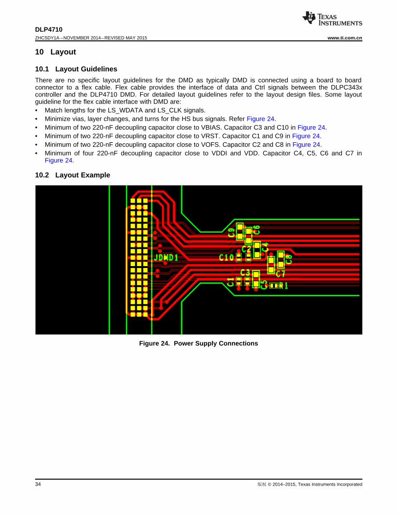
10.1 Layout GuidelinesThere are no specific layout guidelines for the DMD as typically DMD is connected using a board to boardconnector to a flex cable. Flex cable provides the interface of data and Ctrl signals between the DLPC343xcontroller and the DLP4710 DMD. For detailed layout guidelines refer to the layout design files. Some layoutguideline for the flex cable interface with DMD are:• Match lengths for the LS_WDATA and LS_CLK signals.• Minimize vias, layer changes, and turns for the HS bus signals. Refer Figure 24.• Minimum of two 220-nF decoupling capacitor close to VBIAS. Capacitor C3 and C10 in Figure 24.• Minimum of two 220-nF decoupling capacitor close to VRST. Capacitor C1 and C9 in Figure 24.• Minimum of two 220-nF decoupling capacitor close to VOFS. Capacitor C2 and C8 in Figure 24.• Minimum of four 220-nF decoupling capacitor close to VDDI and VDD. Capacitor C4, C5, C6 and C7 in
Figure 24.
10.2 Layout Example
Figure 24. Power Supply Connections
34 版权 © 2014–2015, Texas Instruments Incorporated

DLP4710www.ti.com.cn ZHCSDY1A –NOVEMBER 2014–REVISED MAY 2015
11 器器件件和和文文档档支支持持
11.1 器器件件支支持持
11.1.1 器器件件命命名名规规则则
图图 25. 部部件件号号说说明明
11.1.2 器器件件标标记记
器件标记包括清晰可辨的字符串 GHJJJJK DLP4710FQL。 GHJJJJK 是批次跟踪代码。 DLP4710FQL 是器件标记。
图图 26. DMD 标标记记
11.2 相相关关链链接接
以下表格列出了快速访问链接。 范围包括技术文档、支持与社区资源、工具和软件,并且可以快速访问样片或购买链接。
表表 4. 相相关关链链接接
器器件件 产产品品文文件件夹夹 样样片片与与购购买买 技技术术文文档档 工工具具与与软软件件 支支持持与与社社区区
DLP4710 请单击此处 请单击此处 请单击此处 请单击此处 请单击此处
DLPC3439 请单击此处 单击此处 单击此处 单击此处 单击此处
DLPA3000 单击此处 单击此处 单击此处 单击此处 单击此处
DLPA3005 请单击此处 单击此处 单击此处 单击此处 单击此处
版权 © 2014–2015, Texas Instruments Incorporated 35

DLP4710ZHCSDY1A –NOVEMBER 2014–REVISED MAY 2015 www.ti.com.cn
11.3 社社区区资资源源
The following links connect to TI community resources. Linked contents are provided "AS IS" by the respectivecontributors. They do not constitute TI specifications and do not necessarily reflect TI's views; see TI's Terms ofUse.
TI E2E™ Online Community TI's Engineer-to-Engineer (E2E) Community. Created to foster collaborationamong engineers. At e2e.ti.com, you can ask questions, share knowledge, explore ideas and helpsolve problems with fellow engineers.
Design Support TI's Design Support Quickly find helpful E2E forums along with design support tools andcontact information for technical support.
11.4 商商标标
IntelliBright, E2E are trademarks of Texas Instruments.DLP is a registered trademark of Texas Instruments.All other trademarks are the property of their respective owners.
11.5 静静电电放放电电警警告告
这些装置包含有限的内置 ESD 保护。 存储或装卸时,应将导线一起截短或将装置放置于导电泡棉中,以防止 MOS 门极遭受静电损伤。
11.6 术术语语表表
SLYZ022 — TI 术语表。
这份术语表列出并解释术语、首字母缩略词和定义。
12 机机械械、、封封装装和和可可订订购购信信息息
以下页中包括机械、封装和可订购信息。 这些信息是针对指定器件可提供的最新数据。 这些数据会在无通知且不对本文档进行修订的情况下发生改变。 欲获得该数据表的浏览器版本,请查阅左侧的导航栏。
36 版权 © 2014–2015, Texas Instruments Incorporated

重重要要声声明明
德州仪器(TI) 及其下属子公司有权根据 JESD46 最新标准, 对所提供的产品和服务进行更正、修改、增强、改进或其它更改, 并有权根据JESD48 最新标准中止提供任何产品和服务。客户在下订单前应获取最新的相关信息, 并验证这些信息是否完整且是最新的。所有产品的销售都遵循在订单确认时所提供的TI 销售条款与条件。
TI 保证其所销售的组件的性能符合产品销售时 TI 半导体产品销售条件与条款的适用规范。仅在 TI 保证的范围内,且 TI 认为 有必要时才会使用测试或其它质量控制技术。除非适用法律做出了硬性规定,否则没有必要对每种组件的所有参数进行测试。
TI 对应用帮助或客户产品设计不承担任何义务。客户应对其使用 TI 组件的产品和应用自行负责。为尽量减小与客户产品和应 用相关的风险,客户应提供充分的设计与操作安全措施。
TI 不对任何 TI 专利权、版权、屏蔽作品权或其它与使用了 TI 组件或服务的组合设备、机器或流程相关的 TI 知识产权中授予 的直接或隐含权限作出任何保证或解释。TI 所发布的与第三方产品或服务有关的信息,不能构成从 TI 获得使用这些产品或服 务的许可、授权、或认可。使用此类信息可能需要获得第三方的专利权或其它知识产权方面的许可,或是 TI 的专利权或其它 知识产权方面的许可。
对于 TI 的产品手册或数据表中 TI 信息的重要部分,仅在没有对内容进行任何篡改且带有相关授权、条件、限制和声明的情况 下才允许进行复制。TI 对此类篡改过的文件不承担任何责任或义务。复制第三方的信息可能需要服从额外的限制条件。
在转售 TI 组件或服务时,如果对该组件或服务参数的陈述与 TI 标明的参数相比存在差异或虚假成分,则会失去相关 TI 组件 或服务的所有明示或暗示授权,且这是不正当的、欺诈性商业行为。TI 对任何此类虚假陈述均不承担任何责任或义务。
客户认可并同意,尽管任何应用相关信息或支持仍可能由 TI 提供,但他们将独力负责满足与其产品及在其应用中使用 TI 产品 相关的所有法律、法规和安全相关要求。客户声明并同意,他们具备制定与实施安全措施所需的全部专业技术和知识,可预见 故障的危险后果、监测故障及其后果、降低有可能造成人身伤害的故障的发生机率并采取适当的补救措施。客户将全额赔偿因 在此类安全关键应用中使用任何 TI 组件而对 TI 及其代理造成的任何损失。
在某些场合中,为了推进安全相关应用有可能对 TI 组件进行特别的促销。TI 的目标是利用此类组件帮助客户设计和创立其特 有的可满足适用的功能安全性标准和要求的终端产品解决方案。尽管如此,此类组件仍然服从这些条款。
TI 组件未获得用于 FDA Class III(或类似的生命攸关医疗设备)的授权许可,除非各方授权官员已经达成了专门管控此类使 用的特别协议。
只有那些 TI 特别注明属于军用等级或“增强型塑料”的 TI 组件才是设计或专门用于军事/航空应用或环境的。购买者认可并同 意,对并非指定面向军事或航空航天用途的 TI 组件进行军事或航空航天方面的应用,其风险由客户单独承担,并且由客户独 力负责满足与此类使用相关的所有法律和法规要求。
TI 已明确指定符合 ISO/TS16949 要求的产品,这些产品主要用于汽车。在任何情况下,因使用非指定产品而无法达到 ISO/TS16949 要求,TI不承担任何责任。
产品 应用
数字音频 www.ti.com.cn/audio 通信与电信 www.ti.com.cn/telecom放大器和线性器件 www.ti.com.cn/amplifiers 计算机及周边 www.ti.com.cn/computer数据转换器 www.ti.com.cn/dataconverters 消费电子 www.ti.com/consumer-appsDLP® 产品 www.dlp.com 能源 www.ti.com/energyDSP - 数字信号处理器 www.ti.com.cn/dsp 工业应用 www.ti.com.cn/industrial时钟和计时器 www.ti.com.cn/clockandtimers 医疗电子 www.ti.com.cn/medical接口 www.ti.com.cn/interface 安防应用 www.ti.com.cn/security逻辑 www.ti.com.cn/logic 汽车电子 www.ti.com.cn/automotive电源管理 www.ti.com.cn/power 视频和影像 www.ti.com.cn/video微控制器 (MCU) www.ti.com.cn/microcontrollersRFID 系统 www.ti.com.cn/rfidsysOMAP应用处理器 www.ti.com/omap无线连通性 www.ti.com.cn/wirelessconnectivity 德州仪器在线技术支持社区 www.deyisupport.com
IMPORTANT NOTICE
邮寄地址: 上海市浦东新区世纪大道1568 号,中建大厦32 楼邮政编码: 200122Copyright © 2015, 德州仪器半导体技术(上海)有限公司

PACKAGE OPTION ADDENDUM
www.ti.com 11-Apr-2018
Addendum-Page 1
PACKAGING INFORMATION
Orderable Device Status(1)
Package Type PackageDrawing
Pins PackageQty
Eco Plan(2)
Lead/Ball Finish(6)
MSL Peak Temp(3)
Op Temp (°C) Device Marking(4/5)
Samples
DLP4710FQL ACTIVE CLGA FQL 100 80 RoHS & Green Call TI Level-1-NC-NC
(1) The marketing status values are defined as follows:ACTIVE: Product device recommended for new designs.LIFEBUY: TI has announced that the device will be discontinued, and a lifetime-buy period is in effect.NRND: Not recommended for new designs. Device is in production to support existing customers, but TI does not recommend using this part in a new design.PREVIEW: Device has been announced but is not in production. Samples may or may not be available.OBSOLETE: TI has discontinued the production of the device.
(2) RoHS: TI defines "RoHS" to mean semiconductor products that are compliant with the current EU RoHS requirements for all 10 RoHS substances, including the requirement that RoHS substancedo not exceed 0.1% by weight in homogeneous materials. Where designed to be soldered at high temperatures, "RoHS" products are suitable for use in specified lead-free processes. TI mayreference these types of products as "Pb-Free".RoHS Exempt: TI defines "RoHS Exempt" to mean products that contain lead but are compliant with EU RoHS pursuant to a specific EU RoHS exemption.Green: TI defines "Green" to mean the content of Chlorine (Cl) and Bromine (Br) based flame retardants meet JS709B low halogen requirements of <=1000ppm threshold. Antimony trioxide basedflame retardants must also meet the <=1000ppm threshold requirement.
(3) MSL, Peak Temp. - The Moisture Sensitivity Level rating according to the JEDEC industry standard classifications, and peak solder temperature.
(4) There may be additional marking, which relates to the logo, the lot trace code information, or the environmental category on the device.
(5) Multiple Device Markings will be inside parentheses. Only one Device Marking contained in parentheses and separated by a "~" will appear on a device. If a line is indented then it is a continuationof the previous line and the two combined represent the entire Device Marking for that device.
(6) Lead/Ball Finish - Orderable Devices may have multiple material finish options. Finish options are separated by a vertical ruled line. Lead/Ball Finish values may wrap to two lines if the finishvalue exceeds the maximum column width.
Important Information and Disclaimer:The information provided on this page represents TI's knowledge and belief as of the date that it is provided. TI bases its knowledge and belief on informationprovided by third parties, and makes no representation or warranty as to the accuracy of such information. Efforts are underway to better integrate information from third parties. TI has taken andcontinues to take reasonable steps to provide representative and accurate information but may not have conducted destructive testing or chemical analysis on incoming materials and chemicals.TI and TI suppliers consider certain information to be proprietary, and thus CAS numbers and other limited information may not be available for release.
In no event shall TI's liability arising out of such information exceed the total purchase price of the TI part(s) at issue in this document sold by TI to Customer on an annual basis.

SECTION A-ANOTCH OFFSETS
DETAIL BV-NOTCHSCALE 30 : 1
2 1345678
D
C
B
A
DWG NO. SH8 7 6 5 4 3 1
D
C
B
A
INV11-2006a
2513652 1
TITLE
SIZE DWG NO REV
SCALE SHEET OF
DATE
ENGINEER
QA/CE
CM
APPROVED
DRAWN
INSTRUMENTSDallas Texas
APPLICATIONNEXT ASSY USED ON
THIRD ANGLEPROJECTION
TEXASUNLESS OTHERWISE SPECIFIEDDIMENSIONS ARE IN MILLIMETERSTOLERANCES: ANGLES 1
2 PLACE DECIMALS 0.25
1 PLACE DECIMALS 0.50DIMENSIONAL LIMITS APPLY BEFORE PROCESSESINTERPRET DIMENSIONS IN ACCORDANCE WITH ASME Y14.5M-1994REMOVE ALL BURRS AND SHARP EDGESPARENTHETICAL INFORMATION FOR REFERENCE ONLY
ICD, MECHANICAL, DMD,.47 1080p SERIES 312
(FQL PACKAGE)
25136521 3
DD
2/20/2014
15:1
P. KONRAD
S. SUSI
R. LONG
2/26/2014
2/25/2014
2/26/2014
2/20/2014
0314DA
B. HASKETT
NOTES UNLESS OTHERWISE SPECIFIED:REVISIONSCOPYRIGHT 2014 TEXAS INSTRUMENTS
UN-PUBLISHED, ALL RIGHTS RESERVED.C
B. HASKETT
M. DORAK 2/23/2014
A
A
J J
REV DESCRIPTION DATE BYA ECO 2140050: INITIAL RELEASE 2/20/2014 BMHB ECO 2140429: CORRECT DATUM C IN VIEW J-J, SH. 3 3/6/2014 BMHC ECO 2142093: DELETE BACK SIDE FLATNESS SPEC 5/22/2014 BMHD ECO 2145057: ADD "FQL PACKAGE" TO DRAWING TITLE 7/20/2016 BMH
0.780.063
1.4030.077 1.10.05 D
(2.183)A 3 SURFACES INDICATED
IN VIEW D (SHEET 2)
NOTCH DIMENSIONS ARE DEFINED BY UPPERMOST LAYERS OF CERAMIC, AS SHOWN IN SECTION A-A.
SEE DETAIL B FOR "V-NOTCH" DIMENSIONS.
DIE PARALLELISM TOLERANCE APPLIES TO DMD ACTIVE ARRAY ONLY.
WHILE ONLY THE THREE DATUM A TARGET AREAS A1, A2, AND A3 ARE USED FOR MEASUREMENT, ALL4 CORNERS SHOULD BE CONTACTED, INCLUDING E1, TO SUPPORT MECHANICAL LOADS.
ENCAPSULANT TO BE CONTAINED WITHIN DIMENSIONS SHOWN IN VIEW D (SHEET 2). NOENCAPSULANT IS ALLOWED ON TOP OF THE WINDOW.
ENCAPSULANT NOT TO EXCEED THE HEIGHT OF THE WINDOW.
ROTATION ANGLE OF DMD ACTIVE ARRAY IS A REFINEMENT OF THE LOCATION TOLERANCE AND HASA MAXIMUM ALLOWED VALUE OF 0.6 DEGREES.
BOUNDARY MIRRORS SURROUNDING THE DMD ACTIVE ARRAY.
1
6
5
(ILLUMINATIONDIRECTION)
ACTIVE ARRAY
0.042 A 0.02 D
(SHEET 3)(SHEET 3)
43
(3) 1
4
1(OFF-STATEDIRECTION)
24.5 - 0.10.3+
11 - 0.10.3+
5.5 - 0.10.2+
4X (R0.2)
1.5
(1.6)
0.4 MIN TYP.
0 MIN TYP.
0.188 - 0.10.2+
1
1.60.1
2X ENCAPSULANT
1
1
5
FRONT SIDEINDEX MARK
B
4 - 0.10.2+
30.075
1.5 C
0.4R 0.12X
23.0120.11
1
0.6R 0.1
45°1°
45°1°
(3)
(0.2)2X
(1)
(1.3)
1
1
1
7
8
2
3
4
6
2

VIEW CDATUMS A AND E
(SUBSTRATE METALLIZATION OMITTED FOR CLARITY)(FROM SHEET 1)
VIEW DENCAPSULANT MAXIMUM X/Y DIMENSIONS
(FROM SHEET 1)
VIEW EENCAPSULANT MAXIMUM HEIGHT
2 1345678
D
C
B
A
DWG NO. SH8 7 6 5 4 3 1
D
C
B
A
INV11-2006a
2513652 2
SIZE DWG NO REV
SCALE SHEET OF
DATE
INSTRUMENTSDallas Texas
TEXASDRAWN
25136522 3
DDB. HASKETT 2/20/2014
A3
A2
A1E1
4
11.2
21.5
2X 0 MIN 6
5
2.252X
2.252X
1.3122X 21.52X (1.5)4X
(3.25)4X
1.5
B
1.5
B
1.312
5.6
1.5 C
1.5 C

VIEW FWINDOW AND ACTIVE ARRAY
(FROM SHEET 1)
VIEW J-JBACK SIDE METALLIZATION
(FROM SHEET 1)DETAIL HAPERTURE BOTTOM EDGE
SCALE 60 : 1
DETAIL GAPERTURE TOP EDGE
SCALE 60 : 1
2 1345678
D
C
B
A
DWG NO. SH8 7 6 5 4 3 1
D
C
B
A
INV11-2006a
2513652 3
SIZE DWG NO REV
SCALE SHEET OF
DATE
INSTRUMENTSDallas Texas
TEXASDRAWN
25136523 3
DDB. HASKETT 2/20/2014
H
G
(10.368)ACTIVE ARRAY
(5.832)ACTIVE ARRAY
1.7710.05
8.0090.05
(9.78)WINDOW
12.9920.05
8
7
0.2 A B C0.1 A
(ILLUMINATIONDIRECTION)
(1) 2 3 4 5 6 25 26 27 28 29 (30) (31)
(0.108)4X
(A)
B
C
D
E
F
G
H
J
K
L
3.8940.05
2.9160.075
7.5130.075
0.5750.0635
6.9280.0635
(7.503)APERTURE
11.1860.06350.683±0.0635
(11.869) APERTURE
(16.886) WINDOW
1.5
B
(0.15) TYP.(0.068) TYP.
(42°) TYP. (0.068) TYP.
(0.075) TYP.
1.5
B
20.044827 X 0.7424 =
100X SQUARE LGA PADS0.52±0.05 X 0.52±0.05
(0.52)
16X CIRCULARTEST PADS
BACK SIDEINDEX MARK
SYMBOLIZATION PAD(7 X 3)
1.5 C
2.04
6.6816= 9 X 0.7424
3.341
C1.5
(42°) TYP.(42°) TYP.

重重要要声声明明
德州仪器 (TI) 公司有权按照最新发布的 JESD46 对其半导体产品和服务进行纠正、增强、改进和其他修改,并不再按最新发布的 JESD48 提供任何产品和服务。买方在下订单前应获取最新的相关信息,并验证这些信息是否完整且是最新的。
TI 公布的半导体产品销售条款 (http://www.ti.com/sc/docs/stdterms.htm) 适用于 TI 已认证和批准上市的已封装集成电路产品的销售。另有其他条款可能适用于其他类型 TI 产品及服务的使用或销售。
复制 TI 数据表上 TI 信息的重要部分时,不得变更该等信息,且必须随附所有相关保证、条件、限制和通知,否则不得复制。TI 对该等复制文件不承担任何责任。第三方信息可能受到其它限制条件的制约。在转售 TI 产品或服务时,如果存在对产品或服务参数的虚假陈述,则会失去相关 TI 产品或服务的明示或暗示保证,且构成不公平的、欺诈性商业行为。TI 对此类虚假陈述不承担任何责任。
买方和在系统中整合 TI 产品的其他开发人员(总称“设计人员”)理解并同意,设计人员在设计应用时应自行实施独立的分析、评价和判断,且应全权 负责并确保 应用的安全性, 及设计人员的 应用 (包括应用中使用的所有 TI 产品)应符合所有适用的法律法规及其他相关要求。设计人员就自己设计的 应用声明,其具备制订和实施下列保障措施所需的一切必要专业知识,能够 (1) 预见故障的危险后果,(2) 监视故障及其后果,以及 (3) 降低可能导致危险的故障几率并采取适当措施。设计人员同意,在使用或分发包含 TI 产品的任何 应用前, 将彻底测试该等 应用和 和该等应用所用 TI 产品的 功能而设计。
TI 提供技术、应用或其他设计建议、质量特点、可靠性数据或其他服务或信息,包括但不限于与评估模块有关的参考设计和材料(总称“TI 资源”),旨在帮助设计人员开发整合了 TI 产品的 应用, 如果设计人员(个人,或如果是代表公司,则为设计人员的公司)以任何方式下载、访问或使用任何特定的 TI 资源,即表示其同意仅为该等目标,按照本通知的条款使用任何特定 TI 资源。
TI 所提供的 TI 资源,并未扩大或以其他方式修改 TI 对 TI 产品的公开适用的质保及质保免责声明;也未导致 TI 承担任何额外的义务或责任。TI 有权对其 TI 资源进行纠正、增强、改进和其他修改。除特定 TI 资源的公开文档中明确列出的测试外,TI 未进行任何其他测试。
设计人员只有在开发包含该等 TI 资源所列 TI 产品的 应用时, 才被授权使用、复制和修改任何相关单项 TI 资源。但并未依据禁止反言原则或其他法理授予您任何TI知识产权的任何其他明示或默示的许可,也未授予您 TI 或第三方的任何技术或知识产权的许可,该等产权包括但不限于任何专利权、版权、屏蔽作品权或与使用TI产品或服务的任何整合、机器制作、流程相关的其他知识产权。涉及或参考了第三方产品或服务的信息不构成使用此类产品或服务的许可或与其相关的保证或认可。使用 TI 资源可能需要您向第三方获得对该等第三方专利或其他知识产权的许可。
TI 资源系“按原样”提供。TI 兹免除对资源及其使用作出所有其他明确或默认的保证或陈述,包括但不限于对准确性或完整性、产权保证、无屡发故障保证,以及适销性、适合特定用途和不侵犯任何第三方知识产权的任何默认保证。TI 不负责任何申索,包括但不限于因组合产品所致或与之有关的申索,也不为或对设计人员进行辩护或赔偿,即使该等产品组合已列于 TI 资源或其他地方。对因 TI 资源或其使用引起或与之有关的任何实际的、直接的、特殊的、附带的、间接的、惩罚性的、偶发的、从属或惩戒性损害赔偿,不管 TI 是否获悉可能会产生上述损害赔偿,TI 概不负责。
除 TI 已明确指出特定产品已达到特定行业标准(例如 ISO/TS 16949 和 ISO 26262)的要求外,TI 不对未达到任何该等行业标准要求而承担任何责任。
如果 TI 明确宣称产品有助于功能安全或符合行业功能安全标准,则该等产品旨在帮助客户设计和创作自己的 符合 相关功能安全标准和要求的应用。在应用内使用产品的行为本身不会 配有 任何安全特性。设计人员必须确保遵守适用于其应用的相关安全要求和 标准而设计。设计人员不可将任何 TI 产品用于关乎性命的医疗设备,除非已由各方获得授权的管理人员签署专门的合同对此类应用专门作出规定。关乎性命的医疗设备是指出现故障会导致严重身体伤害或死亡的医疗设备(例如生命保障设备、心脏起搏器、心脏除颤器、人工心脏泵、神经刺激器以及植入设备)。此类设备包括但不限于,美国食品药品监督管理局认定为 III 类设备的设备,以及在美国以外的其他国家或地区认定为同等类别设备的所有医疗设备。
TI 可能明确指定某些产品具备某些特定资格(例如 Q100、军用级或增强型产品)。设计人员同意,其具备一切必要专业知识,可以为自己的应用选择适合的 产品, 并且正确选择产品的风险由设计人员承担。设计人员单方面负责遵守与该等选择有关的所有法律或监管要求。
设计人员同意向 TI 及其代表全额赔偿因其不遵守本通知条款和条件而引起的任何损害、费用、损失和/或责任。IMPORTANT NOTICE
邮寄地址:上海市浦东新区世纪大道 1568 号中建大厦 32 楼,邮政编码:200122Copyright © 2018 德州仪器半导体技术(上海)有限公司