
Dissertation - Max Planck Society · Dissertation submitted to the ... Germaniumdetektoren mit...
160
Dissertation submitted to the Combined Faculties of the Natural Sciences and Mathematics of the Ruperto-Carola-University of Heidelberg. Germany for the degree of Doctor of Natural Sciences Put forward by Marco Salathe born in Seltisberg, Switzerland Oral examination on November 25, 2015
Transcript of Dissertation - Max Planck Society · Dissertation submitted to the ... Germaniumdetektoren mit...
Dissertation
submitted to the
Combined Faculties of the Natural Sciences and Mathematics
of the Ruperto-Carola-University of Heidelberg. Germany
for the degree of
Doctor of Natural Sciences
Put forward by
Marco Salathe
born in Seltisberg, Switzerland
Oral examination on November 25, 2015

Study on modified point contact germanium detectors
for low background applications
Referees:
Prof. Dr. Manfred Lindner
Prof. Dr. Norbert Herrmann

Studie eines modifizierten Germaniumdetektors mit punktformigem Auslesekontakt furAnwendungen bei einem tiefen Untergrund
Germaniumdetektoren mit einer punktformigen Ausleseelektrode (PCGe) spielen bei der Erforschungvon Themen wie dem neutrinolosen doppelten Betazerfall, der direkten Wechselwirkung von dunklerMaterie, dem magnetischen Moment des Neutrinos und der koharenten Streuung von Neutrinos amAtomkern, eine zentrale Rolle. Diese Doktorarbeit prasentiert eine experimentelle Untersuchung vonzwei kommerziell erhaltlichen, fast identischen PCGe-Detektoren mit großem Volumen (∼ 760 g). Diepunktformige Ausleseelektrode wurde, mit Hilfe von spezifischen Simulationen vom elektrischen Feld imDetektor, schrittweise verandert. Die Verkleinerung der fast punktformigen Ausleseelektrode verbessertesowohl die Unterdruckungseffizienz von Untergrundsignalen durch die Analyse der Signalform bei eini-gen MeV wie auch das elektronische Rauschen. Der tiefste Anteil vom Rauschen an der Energieauflosungwar (299 ± 2) eV und (336 ± 2) eV (Halbwertsbreite) fur die beiden Detektoren. Die bessere der bei-den Auflosungen entspricht einer Energieschwelle von 1 keV fur ein Experiment mit einem niedrigenUntergrund. Eine Sensitivitatsstudie kam zu der Schlussfolgerung, dass eine Auflosung von mindestens150−180 eV notig ist, um die koharente Streuung von Neutrinos an Germaniumatomkernen in der Naheeines Atomreaktors zu messen. Das ist ein Faktor zwei besser als das, was bisher erreicht wurde.
Zusatzlich, wurde mit zwei verschiedenen Ansatzen der Fano-Faktor bestimmt. Beide finden ein kon-sistentes Ergebnis, das bessere Ergebnis ist 0.1076± 0.0005. Damit diese optimierten Resultate erreichtwerden konnten, war es wichtig, drei verschiedene Pulsformfilter (der cusp Filter mit abgerundetemMaximum, der trapezoidale Filter mit abgerundetem Maximum und der gaußformige Filter) zusammenmit einer Korrekturmethode fur das ballistische Defizit, zu evaluieren. Danach wurden die als idealbefundenen Filter benutzt, um die Auswertung durchzufuhren.
Study on modified point contact germanium detectors for low background applications
Point contact germanium (PCGe) detectors play a vital role in research such as, neutrinoless doublebeta decay, direct dark matter detection, the neutrino magnetic moment and coherent neutrino-nucleusscattering. This dissertation presents an experimental investigation of two commercially available,almost identical large volume PCGe detectors (∼ 760 g). Their point contact size was stepwise modifiedaccording to specified simulations of the electric field in the detectors. The reduction of the point contactsize improved both, the pulse shape discrimination efficiency of background signals at a few MeV andthe noise from electronics. The lowest contribution of noise to the energy resolution was (299 ± 2) eVand (336± 2) eV (FWHM) for the two detectors, respectively. The better value translates to an energythreshold of 1 keV for an experiment with a low background level. A sensitivity study concluded that aresolution of less than 150− 180 eV is required to detect the coherent neutrino-nucleus scattering nearnuclear reactors. This is a factor of two better than the currently obtained value.
Additionally, two different approaches have been used to determine the Fano factor. They both
yielded consistent results, the better result is 0.1076 ± 0.0005. Before the most optimal results could
be obtained, an evaluation of three shaping filters (the rounded-top cusp, rounded-top trapezoidal
and Gaussian filter) and a ballistic deficit correction was performed. Once completed the most ideal
combinations of filters were used to procure the dissertation’s findings.

Contents
1 Introduction 41.1 Point contact germanium detectors . . . . . . . . . . . . . . . . . . . . . . . . . 4
1.2 PCGe detectors as a gateway to new physics . . . . . . . . . . . . . . . . . . . 4
1.2.1 Coherent Elastic Neutrino-Nucleus Scattering . . . . . . . . . . . . . . . 5
1.2.2 Neutrino magnetic moment . . . . . . . . . . . . . . . . . . . . . . . . . 7
1.2.3 Dark matter detection . . . . . . . . . . . . . . . . . . . . . . . . . . . . 8
1.2.4 Neutrinoless double beta decay . . . . . . . . . . . . . . . . . . . . . . . 10
1.3 A short overview over what follows . . . . . . . . . . . . . . . . . . . . . . . . . 11
2 Germanium detectors 132.1 Radiation and its interaction with matter . . . . . . . . . . . . . . . . . . . . . 13
2.1.1 Heavy charged particles . . . . . . . . . . . . . . . . . . . . . . . . . . . 14
2.1.2 Electrons . . . . . . . . . . . . . . . . . . . . . . . . . . . . . . . . . . . 15
2.1.3 Photons . . . . . . . . . . . . . . . . . . . . . . . . . . . . . . . . . . . . 15
2.1.4 Neutrons . . . . . . . . . . . . . . . . . . . . . . . . . . . . . . . . . . . 18
2.2 Semiconductor physics . . . . . . . . . . . . . . . . . . . . . . . . . . . . . . . . 19
2.2.1 Band structure . . . . . . . . . . . . . . . . . . . . . . . . . . . . . . . . 19
2.2.2 Charge Carrier . . . . . . . . . . . . . . . . . . . . . . . . . . . . . . . . 20
2.2.3 Intrinsic materials and doping . . . . . . . . . . . . . . . . . . . . . . . . 20
2.2.4 pn-junction . . . . . . . . . . . . . . . . . . . . . . . . . . . . . . . . . . 21
2.2.5 Signal formation . . . . . . . . . . . . . . . . . . . . . . . . . . . . . . . 23
2.2.6 Shockley-Ramo Theorem . . . . . . . . . . . . . . . . . . . . . . . . . . 24
2.3 Characteristics of germanium detectors . . . . . . . . . . . . . . . . . . . . . . . 26
2.3.1 Production of germanium detectors . . . . . . . . . . . . . . . . . . . . . 26
2.3.2 Signal variance . . . . . . . . . . . . . . . . . . . . . . . . . . . . . . . . 28
3 Point contact germanium detectors 313.1 Production techniques . . . . . . . . . . . . . . . . . . . . . . . . . . . . . . . . 31
3.2 Existing PCGe detector designs . . . . . . . . . . . . . . . . . . . . . . . . . . . 31
3.3 Capacitance . . . . . . . . . . . . . . . . . . . . . . . . . . . . . . . . . . . . . . 33
3.4 Slow Pulses . . . . . . . . . . . . . . . . . . . . . . . . . . . . . . . . . . . . . . 33
3.4.1 Lithium drift layer . . . . . . . . . . . . . . . . . . . . . . . . . . . . . . 34
3.4.2 Signal formation in the transition layer . . . . . . . . . . . . . . . . . . 35
3.5 Pulse shape discrimination . . . . . . . . . . . . . . . . . . . . . . . . . . . . . . 36
3.5.1 Pulse shape qualifiers . . . . . . . . . . . . . . . . . . . . . . . . . . . . 38
4 Signal acquisition, analysis and simulation 394.1 Electronics . . . . . . . . . . . . . . . . . . . . . . . . . . . . . . . . . . . . . . 39
4.1.1 Electrical components in the frequency domain . . . . . . . . . . . . . . 39
1
Contents
4.1.2 Amplifier . . . . . . . . . . . . . . . . . . . . . . . . . . . . . . . . . . . 40
4.1.3 Response of a charge sensitive preamplifier . . . . . . . . . . . . . . . . 41
4.1.4 Noise in electronics components . . . . . . . . . . . . . . . . . . . . . . . 43
4.1.5 Noise in a charge sensitive preamplifier . . . . . . . . . . . . . . . . . . . 43
4.1.6 Equivalent noise charge . . . . . . . . . . . . . . . . . . . . . . . . . . . 45
4.2 Digital signal processing . . . . . . . . . . . . . . . . . . . . . . . . . . . . . . . 48
4.2.1 Signals and their representation . . . . . . . . . . . . . . . . . . . . . . . 48
4.2.2 Digital linear systems . . . . . . . . . . . . . . . . . . . . . . . . . . . . 49
4.2.3 Pole-zero cancellation . . . . . . . . . . . . . . . . . . . . . . . . . . . . 50
4.2.4 Ballistic deficit correction . . . . . . . . . . . . . . . . . . . . . . . . . . 51
4.2.5 Multi site event correction (MSEC) . . . . . . . . . . . . . . . . . . . . . 53
4.2.6 Optimal filtering . . . . . . . . . . . . . . . . . . . . . . . . . . . . . . . 54
4.2.7 Energy resolution . . . . . . . . . . . . . . . . . . . . . . . . . . . . . . . 55
4.2.8 Energy calibration . . . . . . . . . . . . . . . . . . . . . . . . . . . . . . 57
4.3 Germanium analysis toolkit . . . . . . . . . . . . . . . . . . . . . . . . . . . . . 57
4.3.1 Program organization . . . . . . . . . . . . . . . . . . . . . . . . . . . . 58
4.3.2 Data flow . . . . . . . . . . . . . . . . . . . . . . . . . . . . . . . . . . . 58
4.3.3 Implemented methods . . . . . . . . . . . . . . . . . . . . . . . . . . . . 59
4.3.4 Modular analysis . . . . . . . . . . . . . . . . . . . . . . . . . . . . . . . 60
4.4 Pulse shape simulation . . . . . . . . . . . . . . . . . . . . . . . . . . . . . . . . 62
4.4.1 Field simulation . . . . . . . . . . . . . . . . . . . . . . . . . . . . . . . 62
4.4.2 Charge trajectory . . . . . . . . . . . . . . . . . . . . . . . . . . . . . . 64
5 Point contact optimization 665.1 Simulation-based investigation of geometrical modification . . . . . . . . . . . . 66
5.1.1 Aspect ratio . . . . . . . . . . . . . . . . . . . . . . . . . . . . . . . . . . 67
5.1.2 Impurity concentration . . . . . . . . . . . . . . . . . . . . . . . . . . . 68
5.1.3 Point contact size and groove width . . . . . . . . . . . . . . . . . . . . 69
5.2 Experimental study of point contact detectors . . . . . . . . . . . . . . . . . . . 71
5.2.1 Purchased detectors and their configurations . . . . . . . . . . . . . . . 71
6 Experimental setup and measurement protocol 756.1 Experimental setup . . . . . . . . . . . . . . . . . . . . . . . . . . . . . . . . . . 75
6.1.1 Cryostat and dewar . . . . . . . . . . . . . . . . . . . . . . . . . . . . . 75
6.1.2 Electronics modules . . . . . . . . . . . . . . . . . . . . . . . . . . . . . 78
6.1.3 Measurement tables . . . . . . . . . . . . . . . . . . . . . . . . . . . . . 78
6.2 Measurement protocol . . . . . . . . . . . . . . . . . . . . . . . . . . . . . . . . 79
6.2.1 Source measurements . . . . . . . . . . . . . . . . . . . . . . . . . . . . 79
6.2.2 Additional measurements . . . . . . . . . . . . . . . . . . . . . . . . . . 80
7 Investigation of filter performances 837.1 Filter performance . . . . . . . . . . . . . . . . . . . . . . . . . . . . . . . . . . 83
7.1.1 Shaping time effects of the pseudo-Gaussian filter . . . . . . . . . . . . . 83
7.1.2 Differences between filters . . . . . . . . . . . . . . . . . . . . . . . . . . 86
7.1.3 Data compression . . . . . . . . . . . . . . . . . . . . . . . . . . . . . . 90
2

Contents
7.2 Measurement of the equivalent noise charge . . . . . . . . . . . . . . . . . . . . 907.2.1 Software generated pulser signals . . . . . . . . . . . . . . . . . . . . . . 917.2.2 Software versus analog generated pulser . . . . . . . . . . . . . . . . . . 927.2.3 Baseline shortening . . . . . . . . . . . . . . . . . . . . . . . . . . . . . . 937.2.4 Special consideration for the MSEC method . . . . . . . . . . . . . . . . 94
7.3 Fano factor . . . . . . . . . . . . . . . . . . . . . . . . . . . . . . . . . . . . . . 957.3.1 Analysis procedure . . . . . . . . . . . . . . . . . . . . . . . . . . . . . . 957.3.2 Energy dependence of the Fano factor . . . . . . . . . . . . . . . . . . . 967.3.3 Global fit of the energy resolution . . . . . . . . . . . . . . . . . . . . . 98
8 Results from the point contact size study 1008.1 Energy resolution . . . . . . . . . . . . . . . . . . . . . . . . . . . . . . . . . . . 100
8.1.1 Low energy region (241Am) . . . . . . . . . . . . . . . . . . . . . . . . . 1008.1.2 High energy region (60Co and 228Th) . . . . . . . . . . . . . . . . . . . . 103
8.2 Equivalent noise charge . . . . . . . . . . . . . . . . . . . . . . . . . . . . . . . 1048.2.1 Shaping time dependency . . . . . . . . . . . . . . . . . . . . . . . . . . 1048.2.2 Behavior of the voltage and current . . . . . . . . . . . . . . . . . . . . 107
8.3 High voltage scans . . . . . . . . . . . . . . . . . . . . . . . . . . . . . . . . . . 1108.3.1 241Am and pulser resolution . . . . . . . . . . . . . . . . . . . . . . . . . 1108.3.2 Relative peak position and pulse rise time . . . . . . . . . . . . . . . . . 113
8.4 Collimated measurements near the surface . . . . . . . . . . . . . . . . . . . . . 1158.4.1 Coincidental measurement with a NaI(Tl) detector . . . . . . . . . . . . 1168.4.2 Relative position . . . . . . . . . . . . . . . . . . . . . . . . . . . . . . . 1168.4.3 Rise time . . . . . . . . . . . . . . . . . . . . . . . . . . . . . . . . . . . 1188.4.4 Effects observed with collimated measurements . . . . . . . . . . . . . . 121
8.5 Pulse shape discrimination . . . . . . . . . . . . . . . . . . . . . . . . . . . . . . 1228.5.1 Calculation of suppression efficiencies . . . . . . . . . . . . . . . . . . . 1228.5.2 Comparison of pulse shape discrimination performance . . . . . . . . . . 122
9 Measurements near the trigger threshold 1269.1 Data acquisition trigger . . . . . . . . . . . . . . . . . . . . . . . . . . . . . . . 126
9.1.1 SIS3301 VME trigger . . . . . . . . . . . . . . . . . . . . . . . . . . . . 1269.1.2 Trigger rate . . . . . . . . . . . . . . . . . . . . . . . . . . . . . . . . . . 1269.1.3 Accidentally triggered signals in the energy spectrum . . . . . . . . . . 1279.1.4 Energy threshold of the two PCGe detectors . . . . . . . . . . . . . . . 1319.1.5 Best limits on energy threshold . . . . . . . . . . . . . . . . . . . . . . . 1319.1.6 The energy threshold dependence on point contact size . . . . . . . . . . 134
9.2 Application in physics research . . . . . . . . . . . . . . . . . . . . . . . . . . . 1369.2.1 Extrapolation to low background levels . . . . . . . . . . . . . . . . . . 1389.2.2 Sensitivity to coherent neutrino-nucleus scattering . . . . . . . . . . . . 1389.2.3 Possible detector improvements . . . . . . . . . . . . . . . . . . . . . . . 141
10 Conclusion 143
Bibliography 147
3
1 Introduction
The origin of germanium detector technologies reaches back over half a decade. Althoughtremendous advances have been made in the meantime, technological developments take placeat a rather slow pace. Particularly in the initial years intensive efforts were undertaken tounderstand these detectors that are currently used in a large range of different fields thatstretch from nuclear physics and safeguard to fundamental research in particle physics. Thisthesis should help paving the way, so that this technology can also be used for many newexciting applications in the future. In order to do so, a particular, relatively new type ofgermanium detector will be studied – point contact germanium (PCGe) detectors.
1.1 Point contact germanium detectors
PCGe detectors, are cylindrical detectors that have been produced from germanium. On onebase of the cylinder they have a circular electrode (contact) embedded. The contact radius isusually kept small – close to point like – which explains the name.
These detectors are the central subject of this thesis. Compared to previous studies, this the-sis tries to take a more systematic approach in studying these detectors. The central questionthat should be answered is how these detectors are affected by changes in their geometry. Inorder to answer this question, special care will be given to the application and implementationof old and new computational methods so that the best performance can be obtained. Signalprocessing will therefore be a recurring subject that is nearly as important as the geometricalstudy itself. The study will additionally address several physics related topics. A materialproperty, the Fano factor in germanium, will be measured and the potential of such detectorsfor the detection of coherent nucleus-neutrino scattering studied.
The point contact design of a germanium detector was first proposed by Luke et al. in 1989under the name low capacitance large volume shaped-field germanium detector [1]. The initialaim of this detector type was to measure dark matter. The detector however suffered fromstrong charge trapping and was not used in actual research. Nevertheless, they reached theiraim to produce a detector with a capacitance of close to 1 pF. Many years later, in 2007,Barbeau et al. [2] brought again up this design for applications in fundamental research. Thistime the detector they tested did not show the problematic trapping effects that Luke et al.observed in their earlier study. The design subsequently has been quickly adopted for variousapplication in fundamental science. This will now be discussed in the next section, before thefocus is shifted away from fundamental science to detector physics.
1.2 PCGe detectors as a gateway to new physics
Point contact detectors are mostly used to study neutrinos and their interactions. Neutrinoproperties that are or have been investigated with PCGe detectors include coherent elastic
4
1.2 PCGe detectors as a gateway to new physics
10−3
10−2
10−1
10+0
10+1
10+2
10+3
10+4
0.01 0.1 1 10
Recoil energy [keV]
Eve
nts
[1/k
eV/d
ay/k
g]
Magnetic moment interaction of ν with e−
Standard model interaction of ν with e−
Coherent neutrino nucleus scattering
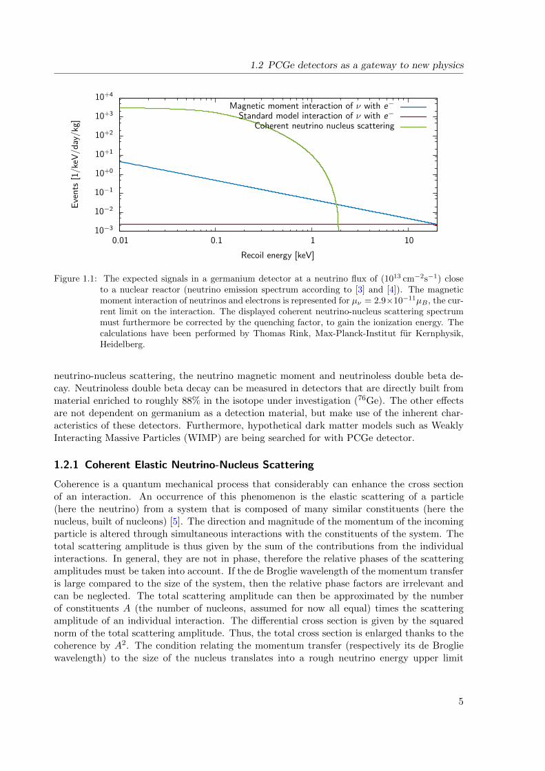
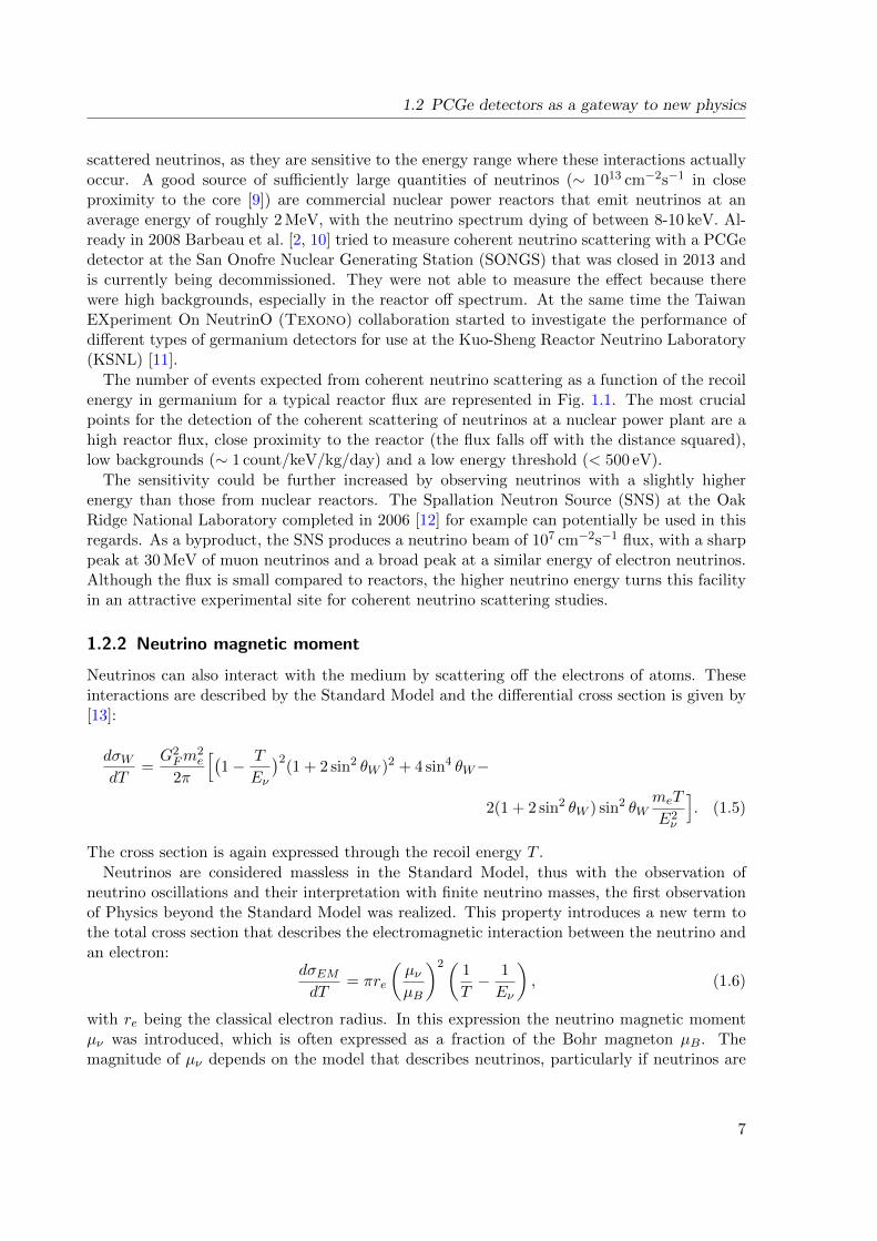
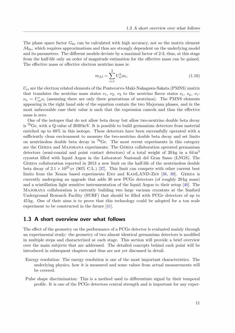
Figure 1.1: The expected signals in a germanium detector at a neutrino flux of (1013 cm−2s−1) closeto a nuclear reactor (neutrino emission spectrum according to [3] and [4]). The magneticmoment interaction of neutrinos and electrons is represented for µν = 2.9×10⁻¹¹µB , the cur-rent limit on the interaction. The displayed coherent neutrino-nucleus scattering spectrummust furthermore be corrected by the quenching factor, to gain the ionization energy. Thecalculations have been performed by Thomas Rink, Max-Planck-Institut fur Kernphysik,Heidelberg.
neutrino-nucleus scattering, the neutrino magnetic moment and neutrinoless double beta de-cay. Neutrinoless double beta decay can be measured in detectors that are directly built frommaterial enriched to roughly 88% in the isotope under investigation (76Ge). The other effectsare not dependent on germanium as a detection material, but make use of the inherent char-acteristics of these detectors. Furthermore, hypothetical dark matter models such as WeaklyInteracting Massive Particles (WIMP) are being searched for with PCGe detector.
1.2.1 Coherent Elastic Neutrino-Nucleus Scattering
Coherence is a quantum mechanical process that considerably can enhance the cross sectionof an interaction. An occurrence of this phenomenon is the elastic scattering of a particle(here the neutrino) from a system that is composed of many similar constituents (here thenucleus, built of nucleons) [5]. The direction and magnitude of the momentum of the incomingparticle is altered through simultaneous interactions with the constituents of the system. Thetotal scattering amplitude is thus given by the sum of the contributions from the individualinteractions. In general, they are not in phase, therefore the relative phases of the scatteringamplitudes must be taken into account. If the de Broglie wavelength of the momentum transferis large compared to the size of the system, then the relative phase factors are irrelevant andcan be neglected. The total scattering amplitude can then be approximated by the numberof constituents A (the number of nucleons, assumed for now all equal) times the scatteringamplitude of an individual interaction. The differential cross section is given by the squarednorm of the total scattering amplitude. Thus, the total cross section is enlarged thanks to thecoherence by A2. The condition relating the momentum transfer (respectively its de Brogliewavelength) to the size of the nucleus translates into a rough neutrino energy upper limit
5
1 Introduction
of 50 MeV [6]. Above this energy the neutrino actually sees the constituents of the nucleusand coherence is not assured. A nucleus is built of protons and neutrons, thus the scatteringamplitudes of the two types of constituent are different and they must be considered separately.
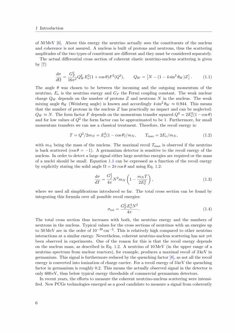
The actual differential cross section of coherent elastic neutrino-nucleus scattering is givenby [7]:
dσ
dΩ=
G2F
16π2Q2WE
2ν(1 + cos θ)F 2(Q2), QW =
[N − (1− 4 sin2 θW )Z
]. (1.1)
The angle θ was chosen to be between the incoming and the outgoing momentum of theneutrino, Eν is the neutrino energy and GF the Fermi coupling constant. The weak nuclearcharge QW depends on the number of protons Z and neutrons N in the nucleus. The weakmixing angle θW (Weinberg angle) is known and accordingly 4 sin2 θW ≈ 0.944. This meansthat the number of protons in the nucleus Z has practically no impact and can be neglected:QW ≈ N . The form factor F depends on the momentum transfer squared Q2 = 2E2
ν(1− cos θ)and for low values of Q2 the form factor can be approximated to be 1. Furthermore, for smallmomentum transfers we can use a classical treatment. Therefore, the recoil energy is:
T = Q2/2mN = E2ν(1− cos θ)/mN , Tmax = 2Eν/mN , (1.2)
with mN being the mass of the nucleus. The maximal recoil Tmax is observed if the neutrinois back scattered (cos θ = −1). A germanium detector is sensitive to the recoil energy of thenucleus. In order to detect a large signal either large neutrino energies are required or the massof a nuclei should be small. Equation 1.1 can be expressed as a function of the recoil energyby explicitly stating the solid angle Ω = 2π cos θ and using Eq. 1.2:
dσ
dT=G2f
4πN2mN
(1− mNT
2E2ν
), (1.3)
where we used all simplifications introduced so far. The total cross section can be found byintegrating this formula over all possible recoil energies:
σtot =G2FE
2νN
2
4π. (1.4)
The total cross section thus increases with both, the neutrino energy and the numbers ofneutrons in the nucleus. Typical values for the cross sections of neutrinos with an energies upto 50 MeV are in the order of 10−39 cm−2. This is relatively high compared to other neutrinointeractions at a similar energy. Nevertheless, coherent neutrino-nucleus scattering has not yetbeen observed in experiments. One of the reason for this is that the recoil energy dependson the nucleus mass, as described in Eq. 1.2. A neutrino of 10 MeV (in the upper range of aneutrino spectrum from nuclear reactors), for example, produces a maximal recoil of 3 keV ingermanium. This signal is furthermore reduced by the quenching factor [8], as not all the recoilenergy is converted into ionization of charge carrier. For a recoil energy of 3 keV the quenchingfactor in germanium is roughly 0.2. This means the actually observed signal in the detector isonly 600 eV, thus below typical energy thresholds of commercial germanium detectors.
In recent years, the efforts to measure the coherent neutrino-nucleus scattering were intensi-fied. New PCGe technologies emerged as a good candidate to measure a signal from coherently
6
1.2 PCGe detectors as a gateway to new physics
scattered neutrinos, as they are sensitive to the energy range where these interactions actuallyoccur. A good source of sufficiently large quantities of neutrinos (∼ 1013 cm−2s−1 in closeproximity to the core [9]) are commercial nuclear power reactors that emit neutrinos at anaverage energy of roughly 2 MeV, with the neutrino spectrum dying of between 8-10 keV. Al-ready in 2008 Barbeau et al. [2, 10] tried to measure coherent neutrino scattering with a PCGedetector at the San Onofre Nuclear Generating Station (SONGS) that was closed in 2013 andis currently being decommissioned. They were not able to measure the effect because therewere high backgrounds, especially in the reactor off spectrum. At the same time the TaiwanEXperiment On NeutrinO (Texono) collaboration started to investigate the performance ofdifferent types of germanium detectors for use at the Kuo-Sheng Reactor Neutrino Laboratory(KSNL) [11].
The number of events expected from coherent neutrino scattering as a function of the recoilenergy in germanium for a typical reactor flux are represented in Fig. 1.1. The most crucialpoints for the detection of the coherent scattering of neutrinos at a nuclear power plant are ahigh reactor flux, close proximity to the reactor (the flux falls off with the distance squared),low backgrounds (∼ 1 count/keV/kg/day) and a low energy threshold (< 500 eV).
The sensitivity could be further increased by observing neutrinos with a slightly higherenergy than those from nuclear reactors. The Spallation Neutron Source (SNS) at the OakRidge National Laboratory completed in 2006 [12] for example can potentially be used in thisregards. As a byproduct, the SNS produces a neutrino beam of 107 cm−2s−1 flux, with a sharppeak at 30 MeV of muon neutrinos and a broad peak at a similar energy of electron neutrinos.Although the flux is small compared to reactors, the higher neutrino energy turns this facilityin an attractive experimental site for coherent neutrino scattering studies.
1.2.2 Neutrino magnetic moment
Neutrinos can also interact with the medium by scattering off the electrons of atoms. Theseinteractions are described by the Standard Model and the differential cross section is given by[13]:
dσWdT
=G2Fm
2e
2π
[(1− T
Eν
)2(1 + 2 sin2 θW )2 + 4 sin4 θW−
2(1 + 2 sin2 θW ) sin2 θWmeT
E2ν
]. (1.5)
The cross section is again expressed through the recoil energy T .
Neutrinos are considered massless in the Standard Model, thus with the observation ofneutrino oscillations and their interpretation with finite neutrino masses, the first observationof Physics beyond the Standard Model was realized. This property introduces a new term tothe total cross section that describes the electromagnetic interaction between the neutrino andan electron:
dσEMdT
= πre
(µνµB
)2( 1
T− 1
Eν
), (1.6)
with re being the classical electron radius. In this expression the neutrino magnetic momentµν was introduced, which is often expressed as a fraction of the Bohr magneton µB. Themagnitude of µν depends on the model that describes neutrinos, particularly if neutrinos are
7
1 Introduction
assumed to be Dirac or Majorana particles. In a minimally extended Standard Model withDirac neutrinos the neutrino magnetic moment is related to the neutrino mass mν and foundto be [14]:
µν ≈ 3× 10⁻¹⁹µB ·mν
1eV. (1.7)
This value is many magnitudes smaller than the sensitivity of any current experiment. Somespecial models describing Physics beyond the Standard Model are predicting a neutrino mag-netic moments up to a level of 10−10 − 10−12 µB [15].
When investigating Eq. 1.5 and 1.6 it is obvious that the cross section dependence on therecoil energy is quite different for the two contributions. The Standard Model cross sectionis nearly constant at low recoil energies, while the electromagnetic cross section has a strong1/T -dependence. This difference makes it possible to distinguish both processes. Moreover,at low energies the electromagnetic contribution should be larger than the Standard Modelcontribution and thus should be measurable.
Usually, experiments looking for coherent elastic neutrino-nucleus scattering can also exploittheir data to define new upper limits of the neutrino magnetic moment and vice versa. Althoughboth, the Texono collaboration [16] and Barbeau et al. [2], published new upper limits basedon their investigations at nuclear power plants, the best limit of the magnetic moment ismeasured by the Gemma collaboration [17]. Their limit of µν ≤ 2.9 × 10⁻¹¹µB (90% C.L.)was measured with a semi-coaxial HPGe detector at 13.9 m distance of a reactor core at theKalinin Nuclear Power Plant (KNPP). At this location they expect the anti-neutrino flux tobe roughly 2.7× 1013 cm−2s−1. The spectrum that is expected from both the standard modelcontribution and the electromagnetic contribution of the neutrino magnetic moment with avalue of the currently best lower limit is indicated in Fig. 1.1.
It is complicated to improve the experimental limits for the neutrino magnetic moment be-cause the sensitivity roughly scales as (B/(Mt))1/4 [16], where B, M and t are the backgroundlevel, detector mass and measurement time. As all these parameters are taken to the power1/4, improving on any of the typical characteristics of a detector setup only has a small impacton the sensitivity to the magnetic moment. Other possible ways to improve the sensitivity areby using a higher neutrino flux, lower energy threshold and higher neutrino energies that alldo not show the to-the-power-1/4 behavior.
1.2.3 Dark matter detection
Although the appearance of neutrino oscillation was the first prove that there must be Physicsbeyond the Standard Model, there are other strong hints that our current understanding of theuniverse is not complete. One of the indications for this is dark matter (a short comprehensiveoverview is Ref. [19] or [20] and the references therein). It has not yet been detected directly butcosmological data show strong evidence for its existence. Dark matter cannot be of baryonicnature and its distribution in cosmological structures has been established through numericalsimulations and lensing observations. The recent Planck data [21] furthermore shows that itmakes up roughly 85% of all matter in the universe and thus roughly 25% of all energy.
Particle physicists came up with a variety of candidates for dark matter particles, of whichthe Weakly Interacting Massive Particle (WIMP) is the most popular one. Its mass must be inthe range from 50 GeV to a few TeV and as its name suggests it should be detectable throughits weak interaction with baryonic matter. The dark matter density of the Milky Way halo at
8
1.2 PCGe detectors as a gateway to new physics
WIMP Mass [GeV/c2]
Cro
ss−s
ectio
n [c
m2 ] (
norm
alis
ed to
nuc
leon
)
100 101 102 10310−46
10−44
10−42
10−40
10−38
ZEPLIN III
DAMA/LIBRA
CRESST II
NeutrinoBackgroundProjection forDirect Detection
DAMIC I
LUX
XENON100
XENON10-LE
CoGeNTROI
CoGeNTlimit
CDMS-LEEDELWEISS-LE
CDMS+EDELWEISS
CDMS-Si
WIMP Mass [GeV/c2]
Cro
ss−s
ectio
n [c
m2 ] (
norm
alis
ed to
nuc
leon
)101 102 10310−40
10−39
10−38
10−37
10−36
PICASSO
Simple
COUPP
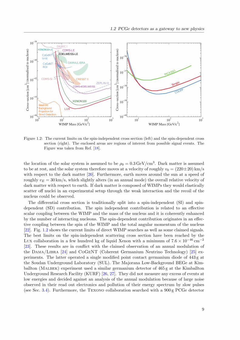
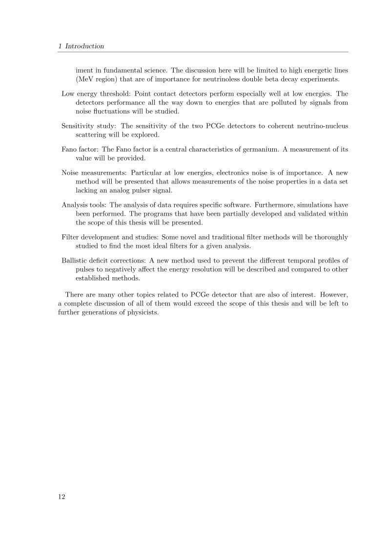
Figure 1.2: The current limits on the spin-independent cross section (left) and the spin-dependent crosssection (right). The enclosed areas are regions of interest from possible signal events. TheFigure was taken from Ref. [18].
the location of the solar system is assumed to be ρ0 = 0.3 GeV/cm3. Dark matter is assumedto be at rest, and the solar system therefore moves at a velocity of roughly v0 = (220±20) km/swith respect to the dark matter [20]. Furthermore, earth moves around the sun at a speed ofroughly vE = 30 km/s, which slightly alters (in an annual mode) the overall relative velocity ofdark matter with respect to earth. If dark matter is composed of WIMPs they would elasticallyscatter off nuclei in an experimental setup through the weak interaction and the recoil of thenucleus could be observed.
The differential cross section is traditionally split into a spin-independent (SI) and spin-dependent (SD) contribution. The spin independent contribution is related to an effectivescalar coupling between the WIMP and the mass of the nucleus and it is coherently enhancedby the number of interacting nucleons. The spin-dependent contribution originates in an effec-tive coupling between the spin of the WIMP and the total angular momentum of the nucleus[22]. Fig. 1.2 shows the current limits of direct WIMP searches as well as some claimed signals.The best limits on the spin-independent scattering cross section have been reached by theLux collaboration in a few hundred kg of liquid Xenon with a minimum of 7.6 × 10−46 cm−2
[23]. These results are in conflict with the claimed observation of an annual modulation ofthe Dama/Libra [24] and CoGeNT (Coherent Germanium Neutrino Technology) [25] ex-periments. The latter operated a single modified point contact germanium diode of 443 g atthe Soudan Underground Laboratory (SUL). The Majorana Low-Background BEGe at Kim-ballton (Malbek) experiment used a similar germanium detector of 465 g at the KimballtonUnderground Research Facility (KURF) [26, 27]. They did not measure any excess of events atlow energies and decided against an analysis of the annual modulation because of large noiseobserved in their read out electronics and pollution of their energy spectrum by slow pulses(see Sec. 3.4). Furthermore, the Texono collaboration searched with a 900 g PCGe detector
9
1 Introduction
at the Kuo-Sheng Reactor Neutrino Laboratory [28] and the China Dark Matter Experiment(Cdex) with two 1 kg PCGe detectors at the China Jinping Underground Laboratory (CJPL)[29] for a WIMP signal and did both exclude the CoGeNT region. Recent new results fromthe Xenon100 collaboration further disfavor models that tried to explain the discrepanciesbetween the different experiments, suggesting that the observed signals might be due to unac-counted systematics [30].
Although the high resolution and low energy threshold of PCGe is very favorable, it mustbe considered that the detected signal is reduced by the quenching factor, as the recoil ofthe nucleus does not directly translate to an ionization signal. This drawback is addressed incryogenic experiments (Cdms,Edelweiss) that run weakly biased germanium detectors at mKtemperatures, so that the phonon signal together with the ionization signal can be detected[31, 32].
The best limits on the spin-dependent cross sections are less stringent and are found primarilyin bubble chamber experiments with fluorine, because the isotope 19F is particularly sensitiveto the spin-dependent interaction. Limits in the range of 10−38 cm−2 were measured by theSimple and Coup collaborations [33, 34] (see also Fig. 1.2).
1.2.4 Neutrinoless double beta decay
Neutrinoless double beta decay is characterized by a final nucleus with an increased protonnumber by two units and the emission of two electrons:
(A,Z)→ (A,Z + 2) + 2e−. (1.8)
Compared to the two-neutrino double beta decay, which additionally involves the emissionof two anti-neutrinos, lepton number is violated in this process. It has been noted that theobservation of neutrinoless double beta decay implies the existence of a Majorana mass termof neutrinos [35]. This term however can be as small as 10−23 eV and in this case it is toosmall to explain the observed neutrino flavor oscillations [36]. Therefore the two phenomenamust not be directly linked and even if neutrinoless double beta decay is observed the neutrinocould still be a Dirac particle. In such a scenario lepton number violation must be caused byanother process that could be studied at locations such as the Large Hadron Collider (LHC).The standard interpretation of the decay is that it is mediated by two light massive Majorananeutrinos and in the following discussion only that case will be considered.
The two-neutrino double beta decay can be observed in 35 even-even isotopes that do notallow the normal beta decay. Their ground states are energetically lower than their odd-oddneighbors. They however allow two beta decays to happen simultaneously. In that case thefinal state is at a lower energy. The two neutrinos carry some of the energy, which currentlycannot be measured. Thus only the sum of the energy of the two electrons is observable asa continuous spectrum. If it exists, neutrinoless double beta decay could also be observed inthese isotopes. There are no neutrinos created in this process, thus the total energy would beseen in the electron signal and the decay would create a sharp line at the Q-value of the decayQββ .
The decay is characterized by its half-life T 0ν1/2, which is found to be inversely proportional
to the square of the effective mass mββ divided by the square of the electron mass me:(T 0ν
1/2
)−1= G0ν(Qββ ,Z) |M0ν |2
(mββ
me
)2
. (1.9)
10
1.3 A short overview over what follows
The phase space factor G0ν can be calculated with high accuracy, not so the matrix elementM0ν , which requires approximations and thus are strongly dependent on the underlying modeland its parameters. The different models deviate by a maximal factor of 2-3, thus, at this stagefrom the half-life only an order of magnitude estimation for the effective mass can be gained.The effective mass or effective electron neutrino mass is:
mββ =3∑i=1
U2eimi. (1.10)
Uei are the electron related elements of the Pontecorvo-Maki-Nakagawa-Sakata (PMNS) matrixthat translates the neutrino mass states ν1, ν2, ν3 to the neutrino flavor states νe, νµ, ντ :να = U∗αiνi (assuming there are only three generations of neutrinos). The PMNS elementsappearing in the right hand side of the equation contain the two Majorana phases, and in themost unfavorable case their value is such that the expression cancels and thus the effectivemass is zero.
One of the isotopes that do not allow beta decay but allow two-neutrino double beta decayis 76Ge, with a Q-value of 2039 keV. It is possible to build germanium detectors from materialenriched up to 88% in this isotope. These detectors have been successfully operated with asufficiently clean environment to measure the two-neutrino double beta decay and set limitson neutrinoless double beta decay in 76Ge. The most recent experiments in this categoryare the Gerda and Majorana experiments. The Gerda collaboration operated germaniumdetectors (semi-coaxial and point contact detectors) of a total weight of 20 kg in a 64 m3
cryostat filled with liquid Argon in the Laboratori Nazionali del Gran Sasso (LNGS). TheGerda collaboration reported in 2013 a new limit on the half-life of the neutrinoless doublebeta decay of 2.1 × 1025 yr (90% C.L.) [37]. This limit can compete with other current bestlimits from the Xenon based experiments Exo and KamLAND-Zen [38, 39]. Gerda iscurrently undergoing an upgrade that adds 30 new PCGe detectors (of roughly 20 kg mass)and a scintillation light sensitive instrumentation of the liquid Argon to their setup [40]. TheMajorana collaboration is currently building two large vacuum cryostats at the SanfordUnderground Research Facility (SURF) that should be filled with PCGe detectors of up to45 kg. One of their aims is to prove that this technology could be adopted for a ton scaleexperiment to be constructed in the future [41].
1.3 A short overview over what follows
The effect of the geometry on the performance of a PCGe detector is evaluated mainly throughan experimental study: the geometry of two almost identical germanium detectors is modifiedin multiple steps and characterized at each stage. This section will provide a brief overviewover the main subjects that are addressed. The detailed concepts behind each point will beintroduced in subsequent chapters and thus are not yet discussed in detail.
Energy resolution: The energy resolution is one of the most important characteristics. Theunderlying physics, how it is measured and some values from actual measurements willbe covered.
Pulse shape discrimination: This is a method used to differentiate signal by their temporalprofile. It is one of the PCGe detectors central strength and is important for any exper-
11
1 Introduction
iment in fundamental science. The discussion here will be limited to high energetic lines(MeV region) that are of importance for neutrinoless double beta decay experiments.
Low energy threshold: Point contact detectors perform especially well at low energies. Thedetectors performance all the way down to energies that are polluted by signals fromnoise fluctuations will be studied.
Sensitivity study: The sensitivity of the two PCGe detectors to coherent neutrino-nucleusscattering will be explored.
Fano factor: The Fano factor is a central characteristics of germanium. A measurement of itsvalue will be provided.
Noise measurements: Particular at low energies, electronics noise is of importance. A newmethod will be presented that allows measurements of the noise properties in a data setlacking an analog pulser signal.
Analysis tools: The analysis of data requires specific software. Furthermore, simulations havebeen performed. The programs that have been partially developed and validated withinthe scope of this thesis will be presented.
Filter development and studies: Some novel and traditional filter methods will be thoroughlystudied to find the most ideal filters for a given analysis.
Ballistic deficit corrections: A new method used to prevent the different temporal profiles ofpulses to negatively affect the energy resolution will be described and compared to otherestablished methods.
There are many other topics related to PCGe detector that are also of interest. However,a complete discussion of all of them would exceed the scope of this thesis and will be left tofurther generations of physicists.
12
2 Germanium detectors
Germanium detectors are semiconductor devices with a pn-junction that are run in the inversebias mode to form a region depleted of free charged particles, that is sensitive to energydeposition from radiation. In this depleted region, incoming radiation can interact with thedetection medium and free previously bound charged particles, which drift in an applied electricfield and induce through their movement a current into the electrode. The current is integratedwith an charge sensitive amplifier and the height of the resulting signal is proportional to theamount of charged particles created in the depleted region and thus proportional to the amountof energy deposited by the radiation. Dedicated electronic circuitry is used to measure thepulse height of these signals and therefore it reconstructs the amount of energy deposited inthe detector.
The first section of this chapter will introduce different types of radiations that can be mea-sured in a germanium detector. This discussion is then followed by a brief outline of physics ofsemiconductors in regards to the usage of such devices in radiation detection applications. Thechapter is concluded with the presentation of some of a germanium detectors characteristics.
2.1 Radiation and its interaction with matter
Although any particle can interact with the material of a germanium detector, the most com-mon application of germanium detectors is spectroscopy, the measurement of photons. Ger-manium has a density that is high compared to silicon, another very common semiconductormaterial and can be produced sufficiently thick (a few centimeters) to also be sensitive tohigh energetic photons (above 1 MeV) that penetrate through thinner and less dense materialswithout interacting with the medium. Germanium detectors are used to detect photons overa broad range of energies, starting from a few keVs up to tens of MeVs. Photons in this rangeare usually characterized as either γ-rays or X-rays, depending on their origin. γ-rays are emit-ted during a radioactive decay of a nucleus, while X-rays are emitted by electrons outside thenucleus. X-rays tend to be found at lower energies than γ-rays, however their typical energyrange overlap. It is therefore not possible to distinguish these two radiations only by the energyof the photon or by the signal they leave in a detection system. Furthermore, the name γ-raysis also used for very high energetic photons (up to the TeV range), which are not considered inthis work. Here γ-rays will only be used to refer to photons that originate from a radioactivedecay and that can be detected with germanium detectors.
Photons are one particular type of radiation, however, next to it there exist other types. Intotal there are 4 categories of radiation that are relevant in γ-ray spectroscopy:
• Heavy charged particles: Ions and α-particles
• Electrons: β-particles
• Photons: X-rays and γ-rays
13
2 Germanium detectors
• Neutrons
Depending on the properties and energy of the penetrating radiation, each of these interactwith the constituents of matter – mainly the electrons and nuclei – through different physicalprocesses. The different processes occur with a certain probability that is governed by the lawsof quantum mechanics and that are described in the framework of quantum field theory by thecross section.
In physics experiments often a large amount of particles interact simultaneously in a medium.A realistic setup thus consists of a particle beam of a flux F hitting a large target. The interac-tion with the target material either deflects the particles from their original path (scattering)or absorbs the particle entirely. The differential cross section, considers this by describing thenumber of particles Ns that are measured at a certain reflection angle per unit time, normalizedby the flux:
dσ
dΩ=Ns
F(2.1)
The incoming flux must be defined as the number of particles per unit time crossing theintersecting area between particle beam and target. The total cross section σtot is calculatedby integrating over all possible angles dΩ = sin θ dθ dφ.
In real situation the target is of a certain thickness, so the total cross section allows tocalculate the amount of particles that are scattered or absorbed over that thickness. In themost simple case (i.e. photons) the probability of a particle penetrating a thickness x of amaterial follows an exponentially decaying function of the form exp(−µx) [42, p. 19]. The factorµ is called the attenuation coefficient and if the material is homogeneous, with a scatteringsite density n then the attenuation coefficient is given by µ = nσtot. The mass attenuationcoefficient µ/ρ is approximately constant for a large range of materials, as the amount ofscattering sites scales roughly with the density of a material.
The total cross section is defined by different physical processes, that in turn are dependenton which type of radiation penetrates what type of material. Thus different types of radiationbehave differently when traveling through germanium.
2.1.1 Heavy charged particles
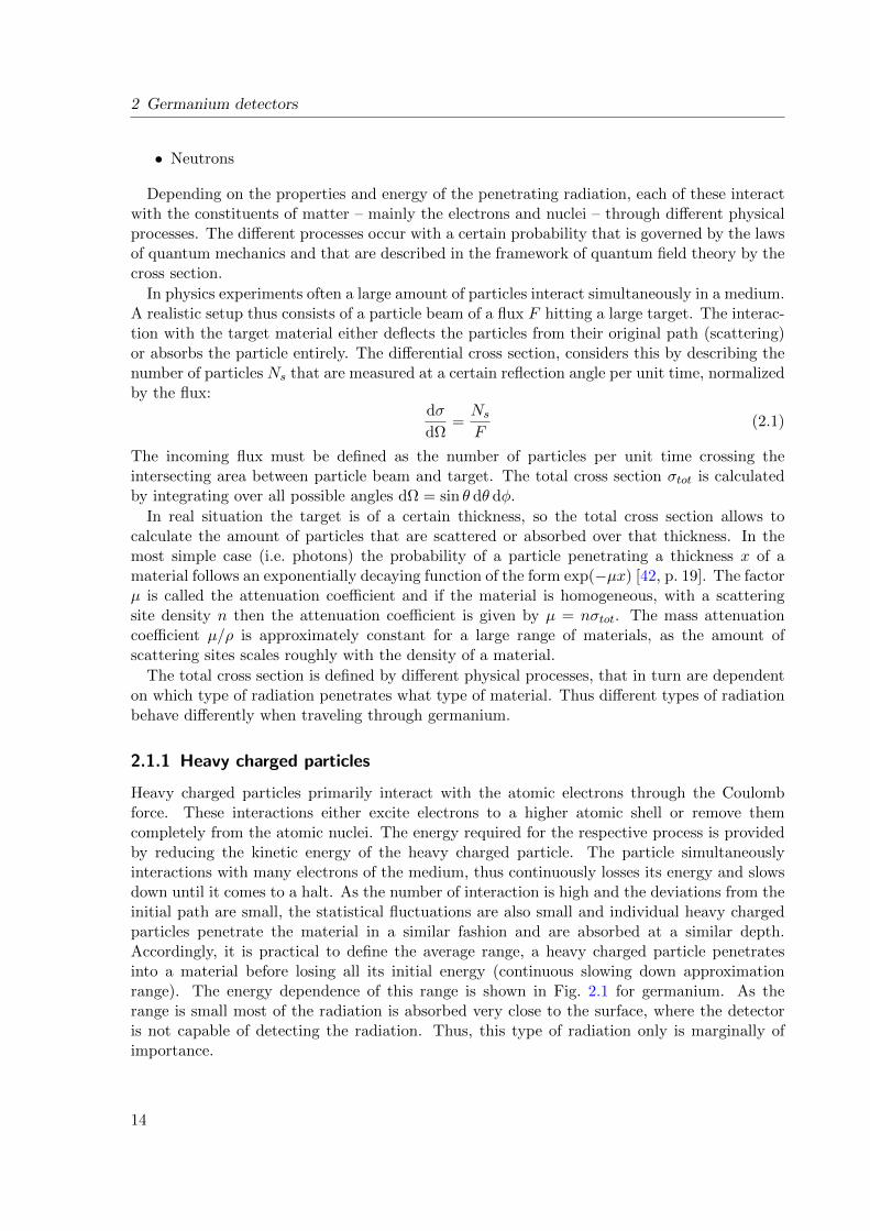
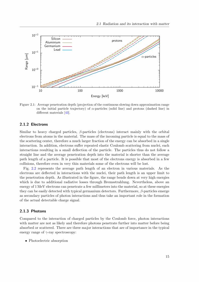
Heavy charged particles primarily interact with the atomic electrons through the Coulombforce. These interactions either excite electrons to a higher atomic shell or remove themcompletely from the atomic nuclei. The energy required for the respective process is providedby reducing the kinetic energy of the heavy charged particle. The particle simultaneouslyinteractions with many electrons of the medium, thus continuously losses its energy and slowsdown until it comes to a halt. As the number of interaction is high and the deviations from theinitial path are small, the statistical fluctuations are also small and individual heavy chargedparticles penetrate the material in a similar fashion and are absorbed at a similar depth.Accordingly, it is practical to define the average range, a heavy charged particle penetratesinto a material before losing all its initial energy (continuous slowing down approximationrange). The energy dependence of this range is shown in Fig. 2.1 for germanium. As therange is small most of the radiation is absorbed very close to the surface, where the detectoris not capable of detecting the radiation. Thus, this type of radiation only is marginally ofimportance.
14
2.1 Radiation and its interaction with matter
10−1
10+0
10+1
10+2
10 100 1000 10000
Ran
ge[µ
m]
Energy [keV]
protons
α-particles
LeadGermaniumAluminium
Silicon
Figure 2.1: Average penetration depth (projection of the continuous slowing down approximation rangeon the initial particle trajectory) of α-particles (solid line) and protons (dashed line) indifferent materials [43].
2.1.2 Electrons
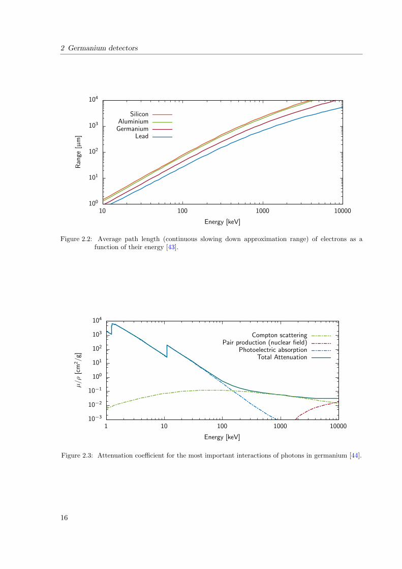
Similar to heavy charged particles, β-particles (electrons) interact mainly with the orbitalelectrons from atoms in the material. The mass of the incoming particle is equal to the mass ofthe scattering center, therefore a much larger fraction of the energy can be absorbed in a singleinteraction. In addition, electrons suffer repeated elastic Coulomb scattering from nuclei, eachinteractions resulting in a small deflection of the particle. The particles thus do not follow astraight line and the average penetration depth into the material is shorter than the averagepath length of a particle. It is possible that most of the electrons energy is absorbed in a fewcollisions, therefore even in very thin materials some of the electrons will be lost.
Fig. 2.2 represents the average path length of an electron in various materials. As theelectrons are deflected in interactions with the nuclei, their path length is an upper limit tothe penetration depth. As illustrated in the figure, the range bends down at very high energieswhich is due to additional radiative losses through Bremsstrahlung. Nevertheless, above anenergy of 1 MeV electrons can penetrate a few millimeters into the material, so at these energiesthey can be easily detected with typical germanium detectors. Furthermore, β-particles emergeas secondary particles of photon interactions and thus take an important role in the formationof the actual detectable charge signal.
2.1.3 Photons
Compared to the interaction of charged particles by the Coulomb force, photon interactionswith matter are not as likely and therefore photons penetrate further into matter before beingabsorbed or scattered. There are three major interactions that are of importance in the typicalenergy range of γ-ray spectroscopy:
• Photoelectric absorption
15
2 Germanium detectors
100
101
102
103
104
10 100 1000 10000
Ran
ge[µ
m]
Energy [keV]
LeadGermaniumAluminium
Silicon
Figure 2.2: Average path length (continuous slowing down approximation range) of electrons as afunction of their energy [43].
10−3
10−2
10−1
100
101
102
103
104
1 10 100 1000 10000
µ/ρ
[cm
2/g
]
Energy [keV]
Total AttenuationPhotoelectric absorption
Pair production (nuclear field)Compton scattering
Figure 2.3: Attenuation coefficient for the most important interactions of photons in germanium [44].
16
2.1 Radiation and its interaction with matter
• Compton scattering
• Pair production
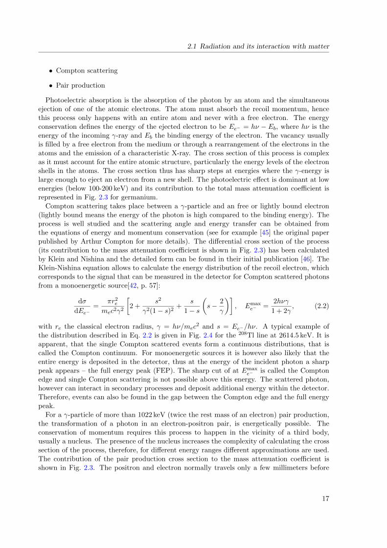
Photoelectric absorption is the absorption of the photon by an atom and the simultaneousejection of one of the atomic electrons. The atom must absorb the recoil momentum, hencethis process only happens with an entire atom and never with a free electron. The energyconservation defines the energy of the ejected electron to be Ee− = hν − Eb, where hν is theenergy of the incoming γ-ray and Eb the binding energy of the electron. The vacancy usuallyis filled by a free electron from the medium or through a rearrangement of the electrons in theatoms and the emission of a characteristic X-ray. The cross section of this process is complexas it must account for the entire atomic structure, particularly the energy levels of the electronshells in the atoms. The cross section thus has sharp steps at energies where the γ-energy islarge enough to eject an electron from a new shell. The photoelectric effect is dominant at lowenergies (below 100-200 keV) and its contribution to the total mass attenuation coefficient isrepresented in Fig. 2.3 for germanium.
Compton scattering takes place between a γ-particle and an free or lightly bound electron(lightly bound means the energy of the photon is high compared to the binding energy). Theprocess is well studied and the scattering angle and energy transfer can be obtained fromthe equations of energy and momentum conservation (see for example [45] the original paperpublished by Arthur Compton for more details). The differential cross section of the process(its contribution to the mass attenuation coefficient is shown in Fig. 2.3) has been calculatedby Klein and Nishina and the detailed form can be found in their initial publication [46]. TheKlein-Nishina equation allows to calculate the energy distribution of the recoil electron, whichcorresponds to the signal that can be measured in the detector for Compton scattered photonsfrom a monoenergetic source[42, p. 57]:
dσ
dEe−=
πr2e
mec2γ2
[2 +
s2
γ2(1− s)2+
s
1− s
(s− 2
γ
)], Emax
e− =2hνγ
1 + 2γ, (2.2)
with re the classical electron radius, γ = hν/mec2 and s = Ee−/hν. A typical example of
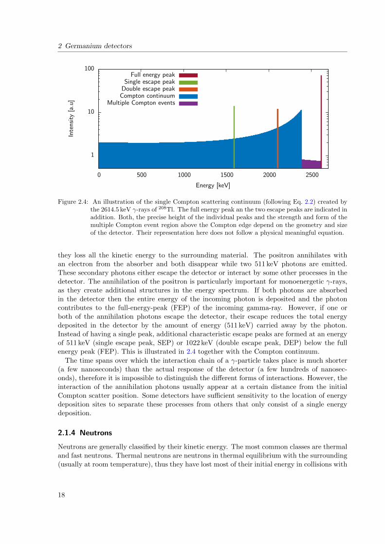
the distribution described in Eq. 2.2 is given in Fig. 2.4 for the 208Tl line at 2614.5 keV. It isapparent, that the single Compton scattered events form a continuous distributions, that iscalled the Compton continuum. For monoenergetic sources it is however also likely that theentire energy is deposited in the detector, thus at the energy of the incident photon a sharppeak appears – the full energy peak (FEP). The sharp cut of at Emax
e− is called the Comptonedge and single Compton scattering is not possible above this energy. The scattered photon,however can interact in secondary processes and deposit additional energy within the detector.Therefore, events can also be found in the gap between the Compton edge and the full energypeak.
For a γ-particle of more than 1022 keV (twice the rest mass of an electron) pair production,the transformation of a photon in an electron-positron pair, is energetically possible. Theconservation of momentum requires this process to happen in the vicinity of a third body,usually a nucleus. The presence of the nucleus increases the complexity of calculating the crosssection of the process, therefore, for different energy ranges different approximations are used.The contribution of the pair production cross section to the mass attenuation coefficient isshown in Fig. 2.3. The positron and electron normally travels only a few millimeters before
17
2 Germanium detectors
1
10
100
0 500 1000 1500 2000 2500
Inte
nsi
ty[a
.u]
Energy [keV]
Multiple Compton eventsCompton continuumDouble escape peakSingle escape peak
Full energy peak
Figure 2.4: An illustration of the single Compton scattering continuum (following Eq. 2.2) created bythe 2614.5 keV γ-rays of 208Tl. The full energy peak an the two escape peaks are indicated inaddition. Both, the precise height of the individual peaks and the strength and form of themultiple Compton event region above the Compton edge depend on the geometry and sizeof the detector. Their representation here does not follow a physical meaningful equation.
they loss all the kinetic energy to the surrounding material. The positron annihilates withan electron from the absorber and both disappear while two 511 keV photons are emitted.These secondary photons either escape the detector or interact by some other processes in thedetector. The annihilation of the positron is particularly important for monoenergetic γ-rays,as they create additional structures in the energy spectrum. If both photons are absorbedin the detector then the entire energy of the incoming photon is deposited and the photoncontributes to the full-energy-peak (FEP) of the incoming gamma-ray. However, if one orboth of the annihilation photons escape the detector, their escape reduces the total energydeposited in the detector by the amount of energy (511 keV) carried away by the photon.Instead of having a single peak, additional characteristic escape peaks are formed at an energyof 511 keV (single escape peak, SEP) or 1022 keV (double escape peak, DEP) below the fullenergy peak (FEP). This is illustrated in 2.4 together with the Compton continuum.
The time spans over which the interaction chain of a γ-particle takes place is much shorter(a few nanoseconds) than the actual response of the detector (a few hundreds of nanosec-onds), therefore it is impossible to distinguish the different forms of interactions. However, theinteraction of the annihilation photons usually appear at a certain distance from the initialCompton scatter position. Some detectors have sufficient sensitivity to the location of energydeposition sites to separate these processes from others that only consist of a single energydeposition.
2.1.4 Neutrons
Neutrons are generally classified by their kinetic energy. The most common classes are thermaland fast neutrons. Thermal neutrons are neutrons in thermal equilibrium with the surrounding(usually at room temperature), thus they have lost most of their initial energy in collisions with
18
2.2 Semiconductor physics
the medium. Fast neutrons have an energy above 1 MeV and usually originate from nuclearreactions. Neutrons interact through the strong force with the nuclei of the absorbing material.This force acts over a very small range, accordingly, the chance of an interaction is relativelysmall. Fast neutrons are mostly elastically or inelastically scattered and thus continuouslyloss kinetic energy to the medium (moderation). In an elastic scattering process, some of theneutron’s kinetic energy is transferred to the recoiling nucleus which partially is convertedinto an ionization signal and thus can be observed in a germanium detector. In the inelasticscattering process the neutron is absorbed and re-emitted at a lower energy, leaving the nucleusin an excited state. The excited nucleus decays after a certain amount of time through theemission of some form of radiation (usually a γ-ray), that can be detected. The most commoninteraction of thermal neutrons is neutron capture by the nucleus, forming an isotope of anincreased mass number by one unit. The final isotope often is found in an excited state, andemits a de-excitation photon. Thermal neutrons furthermore can induce fission, the break upof the nucleus, which is connected with a large release of binding energy.
2.2 Semiconductor physics
In order to understand the functioning of germanium detectors it is required to describe a fewbasic principles from solid state physics. The description here is very limited and will focusmainly on the physics of semiconductors. The discussion is based on Ref. [42, 47, 48] and theinterested reader is referred to these references for more information on the topic.
2.2.1 Band structure
Quantum theory predicts that the wave functions of electrons, that are bound to an atom, canonly be observed in electron shells, quantified energy levels. Each shell holds a fixed numberof electrons; the respective quantum numbers of the system define the number of electronsin each shell and how they are divided into sub-shells. Electrons filling the outer most shellare called valence electrons and define the chemical properties of the element. In solids thewave functions of the valence electrons of neighboring atoms can overlap. The overlappingwave functions cause the energy levels of the valence electrons to be separated, therefore whenatoms are combined in a periodic lattice the discrete energy levels are broadened by the overlapof many different wave functions and energy bands are formed. These bands can overlap (as inmetals) or be separated (as in insulators and semiconductors) and therefore define the electricalproperties of the solid.
Semiconductors need to be build of group 4 elements in the periodic table (octavalent), thatmeans they have 4 valence electrons. The Pauli exclusion principle forces the valence electronsin group 4 elements to be split over two sub-shells (two in the s-state and two in the p-state,both with opposite spins). Therefore the valence electrons take two distinct energy levels, thatare separated from each other, the p-level being the higher of the two. In a semiconductorthe atoms are arranged in a diamond lattice structure and form 4 covalent bonds with theirneighboring atoms. This arrangement in a sufficiently large periodic lattice will broaden thes and p-level into two energy bands: The energetic lower band – the valance band – hasjust enough bonding states to accommodate all the electrons of the lattice. Therefore in theabsences of any excitation no higher energy states are occupied, but also no additional states
19
2 Germanium detectors
are available in the valance band. The higher energetic band – the conduction band – in thissituation is empty.
2.2.2 Charge Carrier
An electron can gain sufficient energy, through thermal motion of the lattice or transferredfrom incident radiation, to leave the covalent bond it is forming with neighboring atoms andby doing so, be elevated from the valence band across the gap into the conduction band. Inthe conduction band, the electron is not bound to the crystal structure and therefore can movefreely through the lattice. The excited electron leaves behind a positively charged vacancy,that can be filled by electrons from neighboring atoms, leaving behind another vacant stateat a different location. Therefore, similar to the free electrons in the conduction band, thisvacant state in the valance band – called ”hole” – can move freely through the crystal, behavingsimilar to a positively charged particle. As each electron moving to the conduction band leavesbehind a hole, the two particles are often referred to as electron-hole pairs or charge carriers.
An electron from the conduction band can fill up a vacant covalent bond and hence recom-bination between an electron and hole occurs. In a pure semiconductor the chance for thisprocess is rather small, therefore the lifetime of the charge carrier can be in theory in theorder of seconds. However, in most semiconductors there is an important amount of impuritiespresent that form so called recombination centers, which capture both electrons and holes andtrap them for a certain amount of time. If two charge carriers of opposite types are capturedsimultaneously they recombine. Such recombination centers are one of the main reasons whyin real semiconductors the lifetime of charge carriers is less than 10−4 s.
2.2.3 Intrinsic materials and doping
The band gap in a semiconductor is relatively large (e.g. 0.7 eV in germanium) comparedto typical thermal energies (i.e. at room temperature, roughly 26 meV). The probability ofoccupying a certain energy state is given by the Fermi-Dirac distribution, thus the probabilityof an electron occupying a state in the conduction band is tiny (4.4×10⁻¹⁰). The high densityof states however assures that electron-hole pairs are constantly being generated. Under theassumption, that no impurities are present in a semiconductor (intrinsic material), the numberof electrons ni and holes pi must be equal (each electron moving to the conduction band leavesbehind a hole in the valence band). The amount of charge carrier is then defined by thetemperature T and the band gap Eg:
np = ni = AT 3/2 exp
(−Eg2kT
), (2.3)
where A is a material dependent constant and k is the Boltzmann constant. As long as theelectrical properties are dominated by this contribution from thermally created charge carriersand not by the amount of impurities in the detector, the material can be considered an intrinsicsemiconductor. A typical value for the numbers of holes/electrons in germanium at 300 K isroughly 2.5× 1013 cm−3.
Some residual impurities are present even in very clear materials. These materials behaveaccording to the dominant type of impurities as either p-type or n-type material:
20
2.2 Semiconductor physics
n-type: The impurities are dominated by group 5 elements (pentavalent), that occupy theplace of a normal group 4 atom (tetravalent). This arrangement results in one of the 5valence electrons of the pentavalent material being incapable of forming a covalent bondwith the surrounding atoms, adding an excess electron to the lattice (donor). The donorelectron is lightly bound to the impurity atom and very little energy is required to breakthe bond and release it into the conduction band. These electrons form energy levels,that lay within the band gap, close to the conduction band (only 0.01 eV below it ingermanium).
p-type: In this case the impurities are dominated by group 3 elements (trivalent), and byreplacing a tetravalent atom they add a vacancy to the lattice structure, which can befilled by a valence electron (acceptor). As the electrons filling the vacancy are only weaklybound to the lattice, their corresponding energy level is in the band gap, just above thevalence band. By borrowing an electron from the lattice they leave behind a hole in thevalence band that can move freely through the crystal structure (hole).
Due to the close proximity of the energy levels formed by the impurities to the respective bands,the thermal energy required to ionize the impurities is very small and all the impurities directlyadd charge carriers to the conduction band of the material. Even at relatively small impurityconcentrations ( 1013 cm−3) these additional charge carriers dominate the conduction band.One type of charge carrier is more prominent (majority carriers) compared to the other type(minority carriers). This shifts the equilibrium between electrons and holes, especially thenumber of recombinations that occur. The number of electrons n and holes p is related to theintrinsic case by the relation n · p = ni · pi.
It is difficult to create materials pure enough to use their intrinsic properties and sometimeseasier to artificially add impurities of the opposite type to compensate for the natural occurringimpurities in those materials (doping). In this way, materials with properties close to intrinsicsemiconductors can be created. The material used in high purity germanium detectors is ofhigh enough purity (impurities of the order of 1010 cm−3) to be considered intrinsic and nocompensation is required.
Semiconductor materials can be heavily doped to create layers with a high conductivity thatcan be used as electrical contacts (electrodes). These layers are specifically designated as p+or n+.
2.2.4 pn-junction
The impurities in a semiconductor can easily be controlled, so that the impurities change fromn-type to p-type, forming a pn-junction. The usual technique to reach this goal is to havelithium drift under high temperature into a uniform p-type material. The lithium does notreplace tetravalent atoms in the crystal structure, instead, because of its small size, it occupiesthe space between the atoms of the crystals (interstitial). In sufficiently large amounts themonovalent lithium then can turn the p-type material into n-type material.
At the boundary of the junction, one side is dominated by electrons from donor atoms,while the other side is dominated by holes from acceptor atoms. This situation forces themore abundant particles to diffuse naturally into the region with a low concentration of therespective charge carriers. The diffusion of charge over the boundary creates a region with anet charge on each side of the junction. The build up of this opposing charge creates an electric
21
2 Germanium detectors
potential, consequently an electric field is formed that reduces the tendency for further chargediffusion over the boundary until an equilibrium is reached.
The intermediate region, or depletion region, has very attractive properties for radiationdetection. It is devoided of charge carries and thus forms a capacitor, with the depletedregion being the dielectric layer and the two adjacent undepleted layers being the electrodes.The formation of an electric field over the intermediate region causes any electrons and holesentering this zone (i.e. created through ionization by radiation) to drift along the field gradienttowards the n- or p-region. This motion in the electric field will cause an electrical signal beinginduced into the electrodes, that then can be read out.
The spontaneously formed depletion region is very thin (a few µm) and the potential createdby the charge separation Vi is small (∼1 V). Additionally, the capacitance of such a junction ishigh, so when it is connected to an external read out circuit, the noise properties are quite poor(see Sec. 4.1 for an explanation of the relationship between capacitance and noise). Therefore,such a depletion region is not very practical for radiation detection application. However,the depleted zone can be increased by applying a reverse bias voltage. This means a positivevoltage is applied to the n-type side of the junction in respect to the p-type side. This attractsadditional electrons and holes across the boundary and therefore enhances the naturally formeddepletion region.
The depletion region extends in both direction and the actual extend can be determined inthe simplest (one dimensional pn-junction, extending to infinity in the other two dimensions)case analytically from the Poisson equation (see any of the above mentioned references for thedetails). The depletion width x depends on the donor Nd and acceptor Na concentrations(which here is assumed to be equal to the concentration of the respective charge carriers n andp in the individual layers) and the applied bias voltage Vb:
xn =
√2ε (Vb + Vi)
eNd (1 +Nd/Na), xp =
√2ε (Vb + Vi)
eNa (1 +Na/Nd), (2.4)
with e being the electronic charge and ε the absolute permittivity (dielectric constant) of thematerial. The total width is simply formed by the sum of the two contributions. In Eq. 2.4the voltage created by the thermal diffusion of electrons and holes across the junction Vi canbe neglected then the bias voltage usually is between 1 and 10 kV and therefore much largerthan Vi.
Most detectors are asymmetrically doped. This means a small part of a very lightly dopedmaterial is highly doped, for example p-type material with lithium, turning it into a n+ layer.The depletion layer then extends predominantly into the lightly doped bulk of the detectorand the depletion width is given by:
w ≈ xn =
√2ε (Vb + Vi)
eNd. (2.5)
This is valid for a one dimensional pn-junction, hence the geometry is identical to a simpleparallel plate capacitor. The capacitance is given by:
C =εA
w= A
√εeNd
2 (Vb + Vi). (2.6)
22
2.2 Semiconductor physics
Consequently, by applying a bias voltage the capacitance is reduced, which affects the noisein a system positively (see Sec. 4.1). Furthermore, the bias voltage also increases the driftvelocity of charge carrier created withing the depletion region, hence reducing the chance ofcharge trapping and recombination. Most detectors are of a more complex geometry and theexact relations between the above mentioned variables can only be found through simulationsof the electric potentials.
A tiny residual current can even flow through a highly biased pn-junction. Some current iscaused by thermally created charge carriers in the depleted region. This current thus dependson the band gap and temperature. In germanium the band gap is small, so at room temperaturethe thermal current is large and the detectors need to be cooled to reduce this contributions.Additional current flows over conducting paths that form between the two electrodes on thesurface of the detector material. Great care is given in the fabrication process of semiconductordevices to avoid contaminations on the surface that facilitate the formation of such surfacecurrents, but they can not be removed entirely. These currents (called leakage currents) addto the current that is observed from drifting charges in the depleted region. If leakage currentsare large, tiny fluctuation in the current can be sufficient enough to corrupt the signal comingfrom charge carriers. The surface leakage currents grow with increasing high voltage, therefore,the bias voltage can not take an arbitrary large value. Furthermore, in high electric fields thecharge carriers can gain sufficient energy to create secondary electron-hole pairs, eventuallyleading to a destructive avalanche.
2.2.5 Signal formation
Thermal energy causes charge carriers to move along random tracks, even when an electric fieldis absent. This random motion, generally identified as diffusion, causes the charge carriers tomove from a region of high concentration to regions with lower concentrations. Assuming thecharge carriers being confined to a point like region at t = 0, then after some elapsed time tthe concentration profile forms a Gaussian of variance:
σ =√Dt. (2.7)
The diffusion constant D is a material dependent property.
In the presence of an electric field, the charge carriers move parallel to the electric fieldvector. The drift direction is defined by their charge; electrons move against the field vector,holes follow the field vector. During this motion the charge carriers interact strongly with thecrystal lattice creating phonons (quantized lattice excitations). This causes the charge carriersto slow down and instead of being accelerated infinitely they reach a constant velocity thatdepends on the strength of the applied electric field:
vh = µhE, ve = µeE. (2.8)
The proportionality constant is the mobility µ of the respective particle type. The hole trans-port involves sequential transition probabilities, therefore they tend to move slightly slowerthan the electron. The mobility and the diffusion constant are linked through the Einsteinequation:
µ =e
kTD, (2.9)
23
2 Germanium detectors
where e is the electric charge, k the Boltzmann constant and T the temperature. Typicalvalues for the mobilities are µe = 3.6×104 cm2/V/s and µh = 4.2×104 cm2/V/s in germaniumat 77 K. For high electric fields (E > 103 V/cm) the drift velocity saturates. The saturationvelocity vs is roughly 107 cm/s and reached at an electric fields of 104 V/cm.
Let us consider the situation where diffusion is negligible and the electric field ~E(~x) constantin time and known in the entire detector volume. Furthermore, a certain amount of electron-hole pairs is deposited at t = 0 in the detector. In this situation, the path of the electrons andholes are entirely defined through Eq. 2.8 and the position of the electrons and holes can becalculated at any point in time t > 0 through integration of this equation.
The presence of a moving charged particle induces a current into the electrodes, which canbe monitored by an external read out system. The motion of the charge can be derived fromEq. 2.8. It remains to calculate the current induced into the respective electrode. In generalthis is possible through Gauss law, which relates the total charge Q in a volume to the flux ofthe electric field through the surface S enclosing the volume:
Q =
‹Sε ~E · d~S, (2.10)
where ε is the permittivity of the medium. The above integral can be evaluated at a giventime t, assuming that the charge carriers in the volume are static at that very moment. Thisis the quasi-steady state approximation, which is equivalent to assume, that the electric fieldpropagates instantaneously through the detector volume. This is a good approximation as thespeed of light (at which the electric field propagates) is large compared to the charge carrierdrift velocity in semiconductor detectors. If the surface is chosen such that it encloses theelectrode, then the above equation describes the charge Q on the electrode at each moment intime. It changes as the electric field is altered by the relocation of the charge carrier in time.The integral therefore must be reevaluated for any position of the charge carriers.
2.2.6 Shockley-Ramo Theorem
Fortunately, the calculation of the induced current in Eq. 2.10 can be simplified with theShockley-Ramo theorem, which was discovered by W. Shockley [49] and S. Ramo [50] indepen-dently.
To derive the Shockley-Ramo theorem, let us consider a certain amount of electrodes (in-dividually numbered by the index i) with a surface Si and a fixed potential Vi arbitrarilydistributed over a volume containing stationary space charges defined by the charge densityρ(~x) and a single moving charge q [51]. The potential at any point in the volume is then definedthrough the Poisson equation with Dirichelet boundary conditions:
− ε∇2ϕ = ρ(~x) + qδ(~x− ~x0), φ|Si = Vi (2.11)
The permittivity ε is considered constant, however, it can be proven, that the Shockley-Ramotheorem is also valid in the case of an inhomogeneous permittivity [52]. Because of linearity ϕcan be be split into three distinct parts, that are defined by the following equations:
∇2ϕ0 = 0, ϕ0|Si = Vi (2.12)
∇2ϕs = −ρ(~x)/ε, ϕs|Si = 0 (2.13)
∇2ϕq = −qδ(~x− ~x0)/ε, ϕq|Si = 0 (2.14)
24
2.2 Semiconductor physics
The first equation describes the electric potential ϕ0, caused only by the applied voltage to theelectrodes. The second equation characterizes the electric potential ϕs created by the spacecharge. The third equation expresses the electric potential ϕq related to the charge q. The
electric field is related to the potential ~E(~x) = −∇ϕ(~x), so the induced charge on electrode ican be expressed as a function of these three potentials:
Qi = −‹Si
ε∇ϕ0 · d~Si −‹Si
ε∇ϕs · d~Si −‹Si
ε∇ · ϕqd~Si. (2.15)
The first and second term in this equation are independent of q, therefore they do not add anyvariation to Qi. Variations of Qi and thus of the induced charge are only dependent on theposition of the charge q and its potential distribution in the device.
Let us consider the following fields:
∇2ψi = 0, ψi|Sj = δij , (2.16)
where the second equation expresses that the field ψi related to electrode i is unity on itssurface and zero on the surface of all other electrodes. Furthermore, Green’s second identityis given by: ˚
VΦ∇2Ψ−Ψ∇2ΦdV =
‹S
Φ∂Ψ
∂n−Ψ
∂Φ
∂ndS. (2.17)
Then, as described in Ref. [53], Ψ = ψ(~x) and Φ = ϕq(~x). The volume V is consider to excludethe interior of the electrodes and its surface is accordingly the sum of the surfaces of allelectrodes. With this definition, ∇2Ψ = 0, so the first integral on the left cancels and Φ|S = 0,so the first integral on the right is zero. Additionally, Ψ|S = δij ,
∂Ψ∂n = ∇Ψ · ~n = − ~Eq(~x) · ~n
and ∇2Φ = −qδ(~x− ~x0)/ε, therefore the equation reduces to:
˚Vqψi(~x)δ(~x− ~x0)dV =
∑j
‹Sεδij ~Eq(~x) · ~ndS =
‹Si
ε ~Eq(~x) · d~Si = Qi, (2.18)
where we moved the ε in the first equality from the left hand side to the right hand side. Thesum in the second equality can be removed by evaluating the delta function. The equation ofGauss’s law for the ith electrode will remain, which is simply equal to Qi. The integral on theleft hand side together with the delta function can be removed by setting ψi(~x) to ψi( ~x0). Theequation therefore is:
qψi( ~x0) = Qi. (2.19)
This equation is Shockley-Ramo’s theorem and expresses, that the induced charge Qi for acharge q at ~x0 can be found from the potential ψi which was defined in Eq. 2.16. This potentialis commonly referred to as weighting potential. Once the weighting potential is known, it isstraight forward to calculate the induced charge for any position of the charge.
Taking the time derivative of Eq. 2.19 one finally, finds the induced current Ii = dQi/dt onelectrode i to be related to the weighting field Eψi
(~x) = −∇ψi(~x):
q ~Eψi( ~x0) · ~v = Ii. (2.20)
To derive the left hand side of this equation the chain rule in three dimensions was used.
25
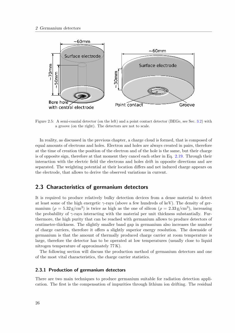
2 Germanium detectors
Figure 2.5: A semi-coaxial detector (on the left) and a point contact detector (BEGe, see Sec. 3.2) witha groove (on the right). The detectors are not to scale.
In reality, as discussed in the previous chapter, a charge cloud is formed, that is composed ofequal amounts of electrons and holes. Electron and holes are always created in pairs, thereforeat the time of creation the position of the electron and of the hole is the same, but their chargeis of opposite sign, therefore at that moment they cancel each other in Eq. 2.19. Through theirinteraction with the electric field the electrons and holes drift in opposite directions and areseparated. The weighting potential at their location differs and net induced charge appears onthe electrode, that allows to derive the observed variations in current.
2.3 Characteristics of germanium detectors
It is required to produce relatively bulky detection devices from a dense material to detectat least some of the high energetic γ-rays (above a few hundreds of keV). The density of ger-manium (ρ = 5.32 g/cm3) is twice as high as the one of silicon (ρ = 2.33 g/cm3), increasingthe probability of γ-rays interacting with the material per unit thickness substantially. Fur-thermore, the high purity that can be reached with germanium allows to produce detectors ofcentimeter-thickness. The slightly smaller band gap in germanium also increases the numberof charge carriers, therefore it offers a slightly superior energy resolution. The downside ofgermanium is that the amount of thermally produced charge carrier at room temperature islarge, therefore the detector has to be operated at low temperatures (usually close to liquidnitrogen temperature of approximately 77 K).
The following section will discuss the production method of germanium detectors and oneof the most vital characteristics, the charge carrier statistics.
2.3.1 Production of germanium detectors
There are two main techniques to produce germanium suitable for radiation detection appli-cation. The first is the compensation of impurities through lithium ion drifting. The residual
26
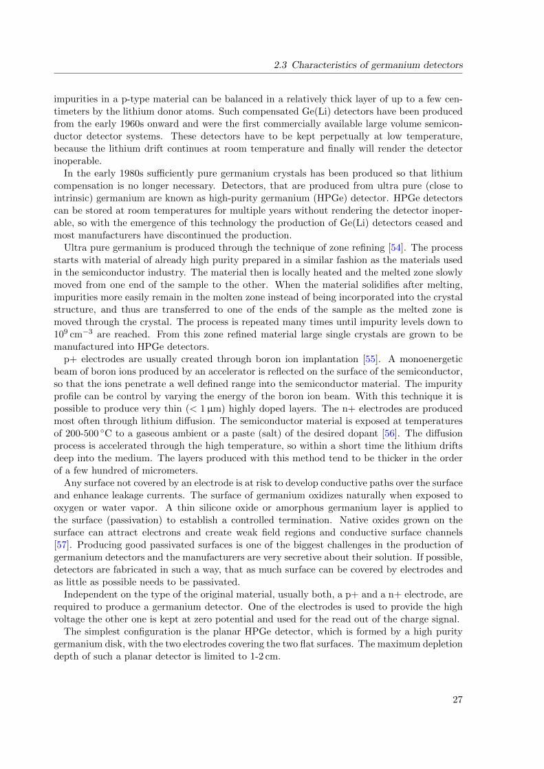
2.3 Characteristics of germanium detectors
impurities in a p-type material can be balanced in a relatively thick layer of up to a few cen-timeters by the lithium donor atoms. Such compensated Ge(Li) detectors have been producedfrom the early 1960s onward and were the first commercially available large volume semicon-ductor detector systems. These detectors have to be kept perpetually at low temperature,because the lithium drift continues at room temperature and finally will render the detectorinoperable.
In the early 1980s sufficiently pure germanium crystals has been produced so that lithiumcompensation is no longer necessary. Detectors, that are produced from ultra pure (close tointrinsic) germanium are known as high-purity germanium (HPGe) detector. HPGe detectorscan be stored at room temperatures for multiple years without rendering the detector inoper-able, so with the emergence of this technology the production of Ge(Li) detectors ceased andmost manufacturers have discontinued the production.
Ultra pure germanium is produced through the technique of zone refining [54]. The processstarts with material of already high purity prepared in a similar fashion as the materials usedin the semiconductor industry. The material then is locally heated and the melted zone slowlymoved from one end of the sample to the other. When the material solidifies after melting,impurities more easily remain in the molten zone instead of being incorporated into the crystalstructure, and thus are transferred to one of the ends of the sample as the melted zone ismoved through the crystal. The process is repeated many times until impurity levels down to109 cm−3 are reached. From this zone refined material large single crystals are grown to bemanufactured into HPGe detectors.
p+ electrodes are usually created through boron ion implantation [55]. A monoenergeticbeam of boron ions produced by an accelerator is reflected on the surface of the semiconductor,so that the ions penetrate a well defined range into the semiconductor material. The impurityprofile can be control by varying the energy of the boron ion beam. With this technique it ispossible to produce very thin (< 1µm) highly doped layers. The n+ electrodes are producedmost often through lithium diffusion. The semiconductor material is exposed at temperaturesof 200-500 C to a gaseous ambient or a paste (salt) of the desired dopant [56]. The diffusionprocess is accelerated through the high temperature, so within a short time the lithium driftsdeep into the medium. The layers produced with this method tend to be thicker in the orderof a few hundred of micrometers.
Any surface not covered by an electrode is at risk to develop conductive paths over the surfaceand enhance leakage currents. The surface of germanium oxidizes naturally when exposed tooxygen or water vapor. A thin silicone oxide or amorphous germanium layer is applied tothe surface (passivation) to establish a controlled termination. Native oxides grown on thesurface can attract electrons and create weak field regions and conductive surface channels[57]. Producing good passivated surfaces is one of the biggest challenges in the production ofgermanium detectors and the manufacturers are very secretive about their solution. If possible,detectors are fabricated in such a way, that as much surface can be covered by electrodes andas little as possible needs to be passivated.
Independent on the type of the original material, usually both, a p+ and a n+ electrode, arerequired to produce a germanium detector. One of the electrodes is used to provide the highvoltage the other one is kept at zero potential and used for the read out of the charge signal.
The simplest configuration is the planar HPGe detector, which is formed by a high puritygermanium disk, with the two electrodes covering the two flat surfaces. The maximum depletiondepth of such a planar detector is limited to 1-2 cm.
27
2 Germanium detectors
0.1330
0.1335
0.1340
0.1345
0.1350
0.1355
0.1360
0.1365
0.1370
102 103 104 1050.6350
0.6355
0.6360
0.6365
0.6370
0.6375
0.6380
0.6385
0.6390
0.6395F
ano
Fac
tor
Yield
Etot/Ethr
Figure 2.6: The Fano factor and yield as a function of the fraction Etot/Ethr derived in a MonteCarlo simulation of the algorithm described in Sec. 2.3.2. At each value the algorithm wasexecuted 106 and the number of charger carriers filled in a histogram. The Fano factor wasthen calculated by F = var(N)/N of the bin distribution and the yield was calculated byN · Ethr/Etot. The error bars assume a normal distribution of the outcome of the varioussimulations.
The active detection volume can be enhanced by bringing the germanium into the form of acoaxial cylinder. This geometry enables the production of detectors with a mass up to 2-3 kg.Here, one electrode covers most of the outer surface of the cylinder, while the other electrodecovers the central hole that passes through the cylinder. Often the hole only extends partiallythrough the cylinder forming a closed-ended coaxial or semi-coaxial detector (see Fig. 2.5),which offers less passivation and a planar front. In this configuration the core electrode iscommonly used for the data read out as the surface is smaller. The down sides of the coaxialconfiguration are reduced resolution caused by a large read out electrode (see Section 4.1).This limitation has been addressed with the introduction of point contact detectors. Similarto the coaxial detector, they have the form of a cylinder but are slightly smaller in diameterand height. Therefore, they don’t need a central core. Instead, they contain a small circularread out electrode on one of the flat surfaces of the cylinder. The remaining surface is coveredby the high voltage electrode. Their name derives from the point like read out electrode andsometimes they are also referred to as (small) point contact detector or p-type point contact(PPC) detectors. The later name indicates that these detector are in general manufacturedfrom p-type high purity germanium. This thesis will be mostly concerned with this type ofdetector, so they will be covered in detail later (see Sec. 3.2).
2.3.2 Signal variance
The incident radiation interacts with the electrons in the medium and transfers part of itsenergy to these electrons, allowing them to move into the conduction band (band gap of 0.7 eVin germanium) and creating an electron-hole-pair that can move freely through the crystallattice. If the initial energy transfer was large enough, these secondary particles can havesufficient kinetic energy to create free electron-hole-pairs themselves. This process initiates a
28

2.3 Characteristics of germanium detectors
cascade of ion pairs, that only ends once the kinetic energy of the secondary particles is too lowto further ionize the medium. This illustrates, that not all the energy of the absorbed radiationis available for the creation of electron-hole-pairs, but some of it appears as a residual kineticenergy of the charge carriers, that is eventually dissipates into lattice vibrations (quantized asphonons). Moreover, in germanium the highest energetic value in the valence band and thelowest energetic value in the conduction band are not found at the same value of momentum inthe phase space. Therefore the transfer of an electron from the valence band to the conductionband, must coincide with a transfer of momentum to a phonon. The energy required forcreating an electron-hole-pair therefore is increased by the amount of energy required for thecreation of phonons.
The final number of charge carrier created by a fixed energy therefore fluctuates. If theindividual electron-hole-pair creation events are independent and have a small constant prob-ability, then the mean number of electron-hole-pairs and the variance can be calculated byapplying Poisson statistics and are given by:
var(N) = N = Etot/ε, (2.21)
where Etot is the total energy deposited in the medium by the radiation and ε is the meanenergy required to produce a single electron-hole-pair. However, the charge carrier creationevents in a germanium detector are not independent of each other. The structure of the cascadeand the mechanism governing the electron-hole-pair creation in a semiconductor needs to betaken into account, causing the observed variance to be smaller than predicted by Poissonstatistics:
F =var(N)
N, 0 < F < 1 (2.22)
The dimensionless Fano factor F was first introduced by Fano in 1947 [58], who tried toexplain the resolution of gas proportional counters. His work was followed by many investi-gations, that primarily focused on understanding the detailed development of the ionizationcascade, including thermal loss to lattice vibrations.
The appearance of a Fano factor below unity can be illustrated by considering a simplemodel that can be easily implemented in a Monte Carlo simulation. Although the modelcan illuminate some of the statistical aspects it is by no mean sufficient to calculate an exactexpression of the Fano factor or explain the main physical mechanism that is responsible forthe appearance of the Fano factor. Sadly, up to now the Fano factor in germanium and othersemiconductors is still not well known and more efforts need to be undertaken to shed some lighton the issue. The simple model that will be studied was initially proposed by van Roosbeck inanalogy of cutting a board in different pieces [59]. The model partitions the total energy Etotof the primary particle in a recursive algorithm and analyze the number of charge carriers thatcan be produced. In each step the energy of a single particle E0 is split up into the energyrequired for the creation of a new electron-hole-pair Ethr and the kinetic energies of the initialand newly formed particles:
1. If E0 < Ethr, then no further charge carriers can be produced, the remaining energy islost to lattice vibration and the algorithm stopped.
2. If E0 > Ethr, then the creation of an new electron-hole-pair is possible, the requiredenergy for the electron-hole-pair creation is subtracted from the total energy (Er =
29
2 Germanium detectors
E0−Ethr). The remaining energy Er is randomly divided into two fractions, the remainingkinetic energy of the primary particle E1, and the shared kinetic energy of the newlycreated electron-hole-pair E2. The latter fraction E2 is furthermore divided (in thesimplest case equally) to form the individual kinetic energy of the electron Ee and holeEh, such that E2 = Ee + Eh.
3. The newly formed fractions E1, Ee and Eh are considered as primaries and step 1 and 2are applied to each piece individually until no further division is possible.
In this manner, the amount of energy deposited by the radiation in the medium is divided intoindividual pieces that can not be further divided and the amount of electron-hole-pairs createdin the process can be estimated. The algorithm with Eh = Ee has been simulated through asmall program (implemented in C) and the results illustrated in Fig. 2.6 for different fractionof Etot/Ethr. It can be seen, that for Etot Ethr both, the Fano factor F = var(N)/N and theyield Y = N ·Ethr/Etot are constant and do neither depend on the total deposited energy northe minimal ionization energy. Even at small values of the ratio Etot/Ethr the deviations froma constant value are small (in the order of 1%), thus also in that range the Fano factor andthe yield can be considered as constant. The value of the Fano factor found with this simplemodel F ∼ 0.13 is in good agreement with values from literature for germanium in the range0.06 to 0.15 (see [60] for a comprehensive overview). The average energy per electron-hole-pairε can be calculated from the yield Y and is ε = Ethr/Y . Assuming Ethr ≈ 1 eV, this wouldmean that the simulated value for the yield is roughly a factor of 2 smaller than what wasfound experimentally (3.6 eV in silicon and 2.96 eV in germanium).
This simple model shows, that a Fano factor much smaller than unity appears naturally if afinite dispersion in the kinetic energy of the charge carrier is assumed. Apart from Monte Carlosimulations, it is possible to describe the effects in an analytic framework and to incorporatephonon losses into the model [59].
Next to this simple model, there are many other models based on similar assumptions,that try to phenomenologically describe the appearance of the Fano factor in semiconductors[60]. Unfortunately, the details of the formation of the ionization cascade, as well as somefundamental aspects of semiconductors are not yet sufficiently well understood to establish asatisfactory description of the Fano factor. Moreover, the reported values from experimentalsetups are found in a relatively large range and discrepancies between measurements have notyet been explained [61]. It has not even been established yet if the Fano factor indeed is amaterial constant or if it changes with energy and temperature as some studies with siliconwould suggest [62].
In chapter 7.3.1 the Fano factor will be experimentally determined and some of the com-plexities that such an evaluation can create will be discussed.
30
3 Point contact germanium detectors
Point contact detectors are cylindrical diodes with a small point contact embedded into one ofthe bases. An example of such a detector is illustrated in Fig. 2.5. The most common applica-tion for PCGe detectors in fundamental research have been described in Sec. 1.2. Their widespread use in these fields is explained by their beneficial properties: They have an exceptionalenergy resolution and low noise. Furthermore, as will be discussed in Sec. 3.5, they allowto distinguish certain types of events solemnly on the time profile of the current pulse. Onemajor drawback is, that they are limited in size. The largest germanium detectors that can beproduced are in the range of 2-3 kg and of a coaxial geometry. It is currently not possible toproduce PCGe detectors of a similar size; the maximal size of these detectors is around 1 kg.
There are PCGe detectors available, that are produced from n-type materials, however mostof the available PCGe detectors are produced from p-type materials, thus only this case willbe considered in the following discussion.
3.1 Production techniques
As discussed in the previous chapter, the two most common production methods of electrodesare lithium diffusion and boron implantation. The lithium diffused layer drops gradually andthe exact depth is relatively hard to control (see Sec. 3.4 for effects caused by this layer). In atypical PCGe detector the lithium diffused electrode covers most of the detectors surface andis used to apply the high voltage.
The boron implantation produces a fast drop over a few hundred of micrometers (usuallyroughly 0.3µm) and is mostly used for the creation of the point contact (although other pro-cedures are also very common). Some of the manufactures remove a thin stripe of a fewmillimeter thickness around the point contact to obtain a better separation between the elec-trodes (groove), others leave the germanium in that region intact. In both cases, the regionbetween the electrodes is passivated to better control conductive paths along the surface.
The size of the detector is mainly limited by the methods available for crystal pulling It ispossible to pull crystals with a radius of more than 4 cm. However, detectors of that size oftenhave weak electric fields (in the corners) with increased charge carrier trapping effects. Largedetectors are also more prone to high leakage currents. Typical large volume HPGe detectorsare produced with a weight between 500 g and 1 kg. The same technology, however, is alsoused to produce detectors of much smaller size.
3.2 Existing PCGe detector designs
There are two major companies producing HPGe detectors; Canberra Industries Inc. [66] andORTEC [67]. Furthermore, there are some smaller companies, such as Baltic Scientific In-struments, Ltd. (BSI) [68], that also have long lasting experience in the production of HPGe
31
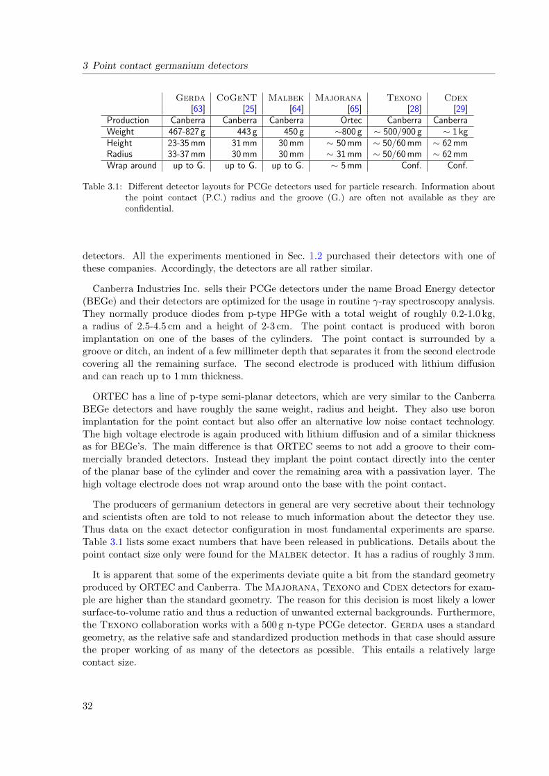
3 Point contact germanium detectors
Gerda CoGeNT Malbek Majorana Texono Cdex[63] [25] [64] [65] [28] [29]
Production Canberra Canberra Canberra Ortec Canberra CanberraWeight 467-827 g 443 g 450 g ∼800 g ∼ 500/900 g ∼ 1 kgHeight 23-35 mm 31 mm 30 mm ∼ 50 mm ∼ 50/60 mm ∼ 62 mmRadius 33-37 mm 30 mm 30 mm ∼ 31 mm ∼ 50/60 mm ∼ 62 mmWrap around up to G. up to G. up to G. ∼ 5 mm Conf. Conf.
Table 3.1: Different detector layouts for PCGe detectors used for particle research. Information aboutthe point contact (P.C.) radius and the groove (G.) are often not available as they areconfidential.
detectors. All the experiments mentioned in Sec. 1.2 purchased their detectors with one ofthese companies. Accordingly, the detectors are all rather similar.
Canberra Industries Inc. sells their PCGe detectors under the name Broad Energy detector(BEGe) and their detectors are optimized for the usage in routine γ-ray spectroscopy analysis.They normally produce diodes from p-type HPGe with a total weight of roughly 0.2-1.0 kg,a radius of 2.5-4.5 cm and a height of 2-3 cm. The point contact is produced with boronimplantation on one of the bases of the cylinders. The point contact is surrounded by agroove or ditch, an indent of a few millimeter depth that separates it from the second electrodecovering all the remaining surface. The second electrode is produced with lithium diffusionand can reach up to 1 mm thickness.
ORTEC has a line of p-type semi-planar detectors, which are very similar to the CanberraBEGe detectors and have roughly the same weight, radius and height. They also use boronimplantation for the point contact but also offer an alternative low noise contact technology.The high voltage electrode is again produced with lithium diffusion and of a similar thicknessas for BEGe’s. The main difference is that ORTEC seems to not add a groove to their com-mercially branded detectors. Instead they implant the point contact directly into the centerof the planar base of the cylinder and cover the remaining area with a passivation layer. Thehigh voltage electrode does not wrap around onto the base with the point contact.
The producers of germanium detectors in general are very secretive about their technologyand scientists often are told to not release to much information about the detector they use.Thus data on the exact detector configuration in most fundamental experiments are sparse.Table 3.1 lists some exact numbers that have been released in publications. Details about thepoint contact size only were found for the Malbek detector. It has a radius of roughly 3 mm.
It is apparent that some of the experiments deviate quite a bit from the standard geometryproduced by ORTEC and Canberra. The Majorana, Texono and Cdex detectors for exam-ple are higher than the standard geometry. The reason for this decision is most likely a lowersurface-to-volume ratio and thus a reduction of unwanted external backgrounds. Furthermore,the Texono collaboration works with a 500 g n-type PCGe detector. Gerda uses a standardgeometry, as the relative safe and standardized production methods in that case should assurethe proper working of as many of the detectors as possible. This entails a relatively largecontact size.
32
3.3 Capacitance
3.3 Capacitance
In their publication about the shape field detector Luke et al. [1] pointed out that the smallsize of the central electrode leads to a small capacitance, which is particular beneficial forapplications where low noise properties are required. They introduced an approximation thatcan be used for estimating the capacitance of such a detector and that is valid as long as theoutside dimensions of the detector are much larger than the central electrode. In that case thecentral electrode is close to be hemispherical in shape (of radius r) and the following equationcan be found for the capacitance:
C = 2πε0εrr. (3.1)
The free space permittivity ε0 = 8.85× 10⁻¹² F/m and the dielectric constant of the materialεr = 16 are known, thus it can be calculated that the capacitance is rough 5 pF for a radius of5 mm.
The effect of the detectors capacitance on the noise is discussed in Sec. 4.1. It is found thata lower capacitance reduces the noise contribution to the resolution. This is of importancefor low energy applications, where the resolution is dominated by the electronics noise. Athigher energies (MeV region) the contribution from charge carriers statistics (see Sec. 2.3.2)dominates.
The rough estimation proposed by Luke et al. is sufficient to get an order of magnitude ofthe capacitance. If it is required to predict the capacitance of a detector in more detail, it ispossible to derive it from the simulated electric potential in the detector (see Sec. 4.4). Thecalculation starts from Gauss’s law of electricity (Maxwell’s macroscopic equations):
‹S
~D · dS =
‹sε0εr ~E · dS = Q. (3.2)
The integral in this equation describes the flux of the electric field ~E through the surface ofa volume V , which contains a charge Q. ε0 is the vacuum permittivity and εr the relativepermittivity in the material. The above equation also contains contributions from the spacecharges, however, as it has been discussed in Sec. 2.2.6 it is possible to split Eq. 3.2 into thecontributions from the geometry ~E0 and from the space charge ~Ec, which in turn also allowsto split the right hand side of the equation into the respective charge contribution Q0 and Qc.As we are only interested in Q0 the contribution from space charges can be cancelled and wecan calculate the induced charge on the electrode Q0 from the electric field ~E0, without anyspace charges in the detector.
3.4 Slow Pulses
In a PCGe detector the high voltage is applied to the electrode covering most of the outersurface, while the signal is read out at the central point like electrode (p+ contact). Thesurface electrode is produced by lithium diffusion and usually chosen to have a thickness ofthe order of 1 mm. This helps to reduce the background from α and β-particles which can notpenetrate through this layer. γ-rays usually have a penetration depth large enough, so thatthey easily travel through this layer and reach the depleted zone. However, at energies below50 keV the penetration depth is less than a millimeter, therefore some γ-rays do not reach
33
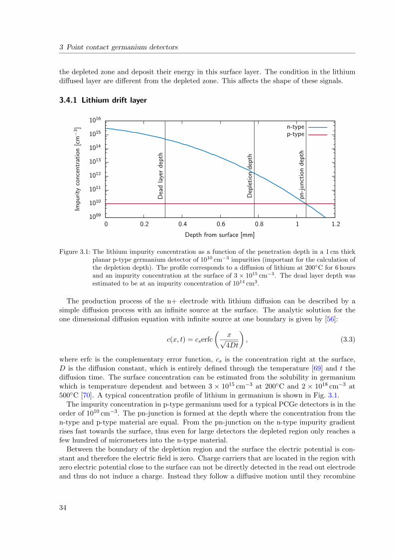
3 Point contact germanium detectors
the depleted zone and deposit their energy in this surface layer. The condition in the lithiumdiffused layer are different from the depleted zone. This affects the shape of these signals.
3.4.1 Lithium drift layer
1009
1010
1011
1012
1013
1014
1015
1016
0 0.2 0.4 0.6 0.8 1 1.2
Imp
uri
tyco
nce
ntr
atio
n[c
m−3]
Depth from surface [mm]
Dea
dla
yer
dep
th
Dep
leti
ond
epth
pn
-ju
nct
ion
dep
th
n-typep-type
Figure 3.1: The lithium impurity concentration as a function of the penetration depth in a 1 cm thickplanar p-type germanium detector of 1010 cm−3 impurities (important for the calculation ofthe depletion depth). The profile corresponds to a diffusion of lithium at 200C for 6 hoursand an impurity concentration at the surface of 3 × 1015 cm−3. The dead layer depth wasestimated to be at an impurity concentration of 1014 cm3.
The production process of the n+ electrode with lithium diffusion can be described by asimple diffusion process with an infinite source at the surface. The analytic solution for theone dimensional diffusion equation with infinite source at one boundary is given by [56]:
c(x, t) = cserfc
(x√4Dt
), (3.3)
where erfc is the complementary error function, cs is the concentration right at the surface,D is the diffusion constant, which is entirely defined through the temperature [69] and t thediffusion time. The surface concentration can be estimated from the solubility in germaniumwhich is temperature dependent and between 3 × 1015 cm−3 at 200C and 2 × 1018 cm−3 at500C [70]. A typical concentration profile of lithium in germanium is shown in Fig. 3.1.
The impurity concentration in p-type germanium used for a typical PCGe detectors is in theorder of 1010 cm−3. The pn-junction is formed at the depth where the concentration from then-type and p-type material are equal. From the pn-junction on the n-type impurity gradientrises fast towards the surface, thus even for large detectors the depleted region only reaches afew hundred of micrometers into the n-type material.
Between the boundary of the depletion region and the surface the electric potential is con-stant and therefore the electric field is zero. Charge carriers that are located in the region withzero electric potential close to the surface can not be directly detected in the read out electrodeand thus do not induce a charge. Instead they follow a diffusive motion until they recombine
34
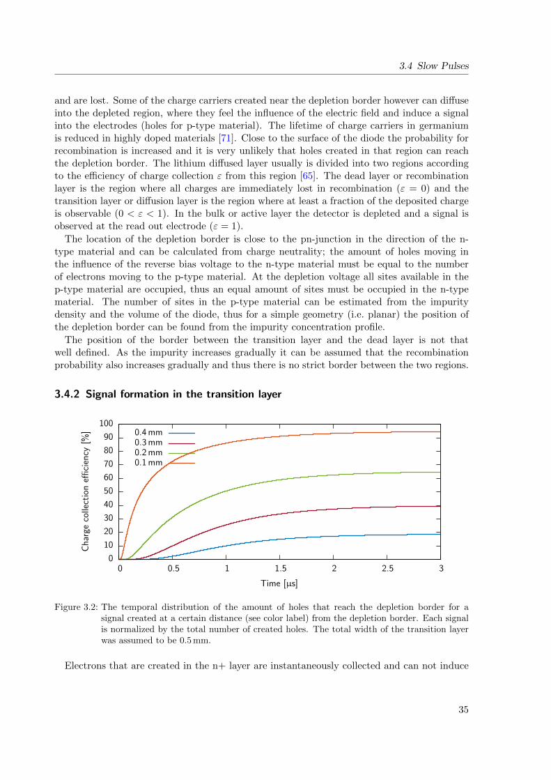
3.4 Slow Pulses
and are lost. Some of the charge carriers created near the depletion border however can diffuseinto the depleted region, where they feel the influence of the electric field and induce a signalinto the electrodes (holes for p-type material). The lifetime of charge carriers in germaniumis reduced in highly doped materials [71]. Close to the surface of the diode the probability forrecombination is increased and it is very unlikely that holes created in that region can reachthe depletion border. The lithium diffused layer usually is divided into two regions accordingto the efficiency of charge collection ε from this region [65]. The dead layer or recombinationlayer is the region where all charges are immediately lost in recombination (ε = 0) and thetransition layer or diffusion layer is the region where at least a fraction of the deposited chargeis observable (0 < ε < 1). In the bulk or active layer the detector is depleted and a signal isobserved at the read out electrode (ε = 1).
The location of the depletion border is close to the pn-junction in the direction of the n-type material and can be calculated from charge neutrality; the amount of holes moving inthe influence of the reverse bias voltage to the n-type material must be equal to the numberof electrons moving to the p-type material. At the depletion voltage all sites available in thep-type material are occupied, thus an equal amount of sites must be occupied in the n-typematerial. The number of sites in the p-type material can be estimated from the impuritydensity and the volume of the diode, thus for a simple geometry (i.e. planar) the position ofthe depletion border can be found from the impurity concentration profile.
The position of the border between the transition layer and the dead layer is not thatwell defined. As the impurity increases gradually it can be assumed that the recombinationprobability also increases gradually and thus there is no strict border between the two regions.
3.4.2 Signal formation in the transition layer
0
10
20
30
40
50
60
70
80
90
100
0 0.5 1 1.5 2 2.5 3
Ch
arge
colle
ctio
neffi
cien
cy[%
]
Time [µs]
0.4 mm0.3 mm0.2 mm0.1 mm
Figure 3.2: The temporal distribution of the amount of holes that reach the depletion border for asignal created at a certain distance (see color label) from the depletion border. Each signalis normalized by the total number of created holes. The total width of the transition layerwas assumed to be 0.5 mm.
Electrons that are created in the n+ layer are instantaneously collected and can not induce
35
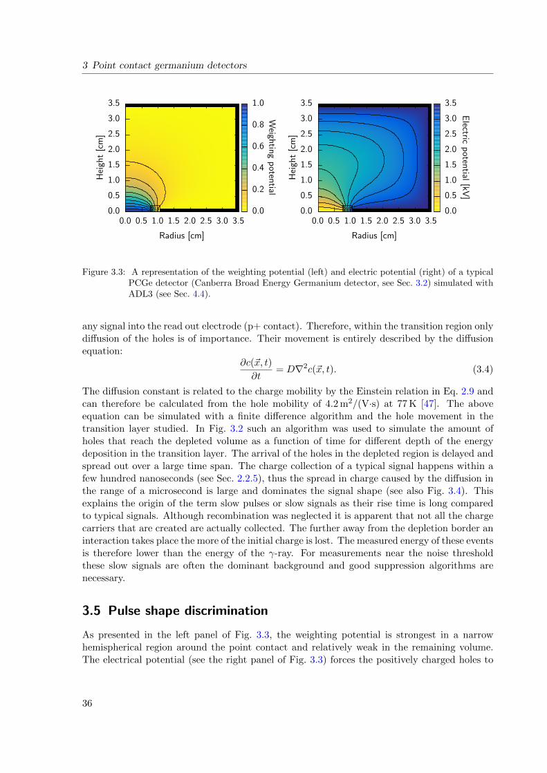
3 Point contact germanium detectors
Radius [cm]
Hei
ght
[cm
]
0.0
0.5
1.0
1.5
2.0
2.5
3.0
3.5
0.0 0.5 1.0 1.5 2.0 2.5 3.0 3.50.0
0.2
0.4
0.6
0.8
1.0
Weigh
ting
poten
tial
Radius [cm]
Hei
ght
[cm
]
0.0
0.5
1.0
1.5
2.0
2.5
3.0
3.5
0.0 0.5 1.0 1.5 2.0 2.5 3.0 3.50.0
0.5
1.0
1.5
2.0
2.5
3.0
3.5
Electric
poten
tial[kV
]
Figure 3.3: A representation of the weighting potential (left) and electric potential (right) of a typicalPCGe detector (Canberra Broad Energy Germanium detector, see Sec. 3.2) simulated withADL3 (see Sec. 4.4).
any signal into the read out electrode (p+ contact). Therefore, within the transition region onlydiffusion of the holes is of importance. Their movement is entirely described by the diffusionequation:
∂c(~x, t)
∂t= D∇2c(~x, t). (3.4)
The diffusion constant is related to the charge mobility by the Einstein relation in Eq. 2.9 andcan therefore be calculated from the hole mobility of 4.2 m2/(V·s) at 77 K [47]. The aboveequation can be simulated with a finite difference algorithm and the hole movement in thetransition layer studied. In Fig. 3.2 such an algorithm was used to simulate the amount ofholes that reach the depleted volume as a function of time for different depth of the energydeposition in the transition layer. The arrival of the holes in the depleted region is delayed andspread out over a large time span. The charge collection of a typical signal happens within afew hundred nanoseconds (see Sec. 2.2.5), thus the spread in charge caused by the diffusion inthe range of a microsecond is large and dominates the signal shape (see also Fig. 3.4). Thisexplains the origin of the term slow pulses or slow signals as their rise time is long comparedto typical signals. Although recombination was neglected it is apparent that not all the chargecarriers that are created are actually collected. The further away from the depletion border aninteraction takes place the more of the initial charge is lost. The measured energy of these eventsis therefore lower than the energy of the γ-ray. For measurements near the noise thresholdthese slow signals are often the dominant background and good suppression algorithms arenecessary.
3.5 Pulse shape discrimination
As presented in the left panel of Fig. 3.3, the weighting potential is strongest in a narrowhemispherical region around the point contact and relatively weak in the remaining volume.The electrical potential (see the right panel of Fig. 3.3) forces the positively charged holes to
36
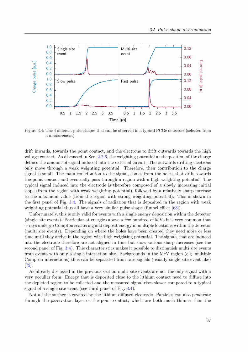
3.5 Pulse shape discrimination
0.0
0.2
0.4
0.6
0.8
1.0
0.00
0.04
0.08
0.12
0.0
0.2
0.4
0.6
0.8
1.0
0.5 1 1.5 2 2.5 3 3.5 0.5 1 1.5 2 2.5 3 3.5
0.00
0.04
0.08
0.12
Ch
arge
pu
lse
[a.u
.]
Cu
rrent
pu
lse[a.u
.]
Time [µs]
Single siteevent
Multi siteevent
Slow pulse Fast pulse
Figure 3.4: The 4 different pulse shapes that can be observed in a typical PCGe detectors (selected froma measurement).
drift inwards, towards the point contact, and the electrons to drift outwards towards the highvoltage contact. As discussed in Sec. 2.2.6, the weighting potential at the position of the chargedefines the amount of signal induced into the external circuit. The outwards drifting electronsonly move through a weak weighting potential. Therefore, their contribution to the chargesignal is small. The main contribution to the signal, comes from the holes, that drift towardsthe point contact and eventually pass through a region with a high weighting potential. Thetypical signal induced into the electrode is therefore composed of a slowly increasing initialslope (from the region with weak weighting potential), followed by a relatively sharp increaseto the maximum value (from the region with strong weighting potential). This is shown inthe first panel of Fig. 3.4. The signals of radiation that is deposited in the region with weakweighting potential thus all have a very similar pulse shape (funnel effect [63]).
Unfortunately, this is only valid for events with a single energy deposition within the detector(single site events). Particular at energies above a few hundred of keVs it is very common thatγ-rays undergo Compton scattering and deposit energy in multiple locations within the detector(multi site events). Depending on where the holes have been created they need more or lesstime until they arrive in the region with high weighting potential. The signals that are inducedinto the electrode therefore are not aligned in time but show various sharp increases (see thesecond panel of Fig. 3.4). This characteristics makes it possible to distinguish multi site eventsfrom events with only a single interaction site. Backgrounds in the MeV region (e.g. multipleCompton interactions) thus can be separated from rare signals (usually single site event like)[72].
As already discussed in the previous section multi site events are not the only signal with avery peculiar form. Energy that is deposited close to the lithium contact need to diffuse intothe depleted region to be collected and the measured signal rises slower compared to a typicalsignal of a single site event (see third panel of Fig. 3.4).
Not all the surface is covered by the lithium diffused electrode. Particles can also penetratethrough the passivation layer or the point contact, which are both much thinner than the
37
3 Point contact germanium detectors
lithium layer. As represented in the fourth panel of Fig. 3.4, these events are characterized bya fast rising pulse shape. In this case also the electron is moving through a high weighting fieldregion and thus its contribution to the signal can not be neglected. The shape of these twosingles deviates from a typical single and multi site event and can therefore be discriminated.
3.5.1 Pulse shape qualifiers
To distinguish the different classes of signals it is convenient to define qualifiers or discrimina-tion parameters. It can be seen in Fig. 3.4 that the most distinct feature between the differentpulse shapes is the time over which the charge pulse rises from the onset of the pulse to itsmaximum value. This is expressed as the rise time and requires to define two confining limits,usually expressed in percents of the pulse height (e.g. 10-90% or 2-70%). However for a noisysignal the pulse height is not very well defined and the limits strongly affected by the noise.For a good estimation of the rise time therefore some filtering before the measurement of therise time is required to reduce the signal-to-noise ratio and allow a meaningful estimation ofthe rise time.
Another method to quantify the differences between the different pulse shapes is to normalizethe current signal and measure the maximal amplitude. Figure 3.4 shows that the maximal am-plitude of the current signal indeed differs considerably between the different pulse shapes. Inorder to normalize the current pulse often the uncalibrated value for the energy (reconstructedpulse height) is used. This explains the origin of the expression amplitude-over-energy or A/E[72]. This procedure allows to get an almost energy independent discrimination parameterfor the different pulse shapes. The resolution of the amplitude measurement can be slightlyimproved by filtering the current pulse before measuring the amplitude (see Sec. 4.2.2).
38
4 Signal acquisition, analysis and simulation
The following chapter will discuss the data processing chain, from data amplification and ac-quisition, based on electronic components, to the filtering techniques applied to the digitizedsignals. New filtering methods and software will be presented in this chapter, that was devel-oped together with collaborators within the scope of this thesis. The software and filter methodswere extensively used in this work for data analysis. Furthermore, the signal formation process,that was discussed in the previous chapter can be implemented into a computational model tosimulate the response of a typical germanium detector and learn more about the performanceof a given system. Such a simulation tool, was adopted from previous work and was tailoredfor the study of germanium detector optimizations. The tool is discussed in the second part ofthis chapter.
4.1 Electronics
Electronic components in radiation detection systems serve three distinct purpose:
1. operation of the semiconductor detection device,
2. amplification of a detector signal,
3. shape the signal into a form to allow a measure of the investigated physical quantity withthe lowest possible signal-to-noise ratio.
The first point is covered by providing the necessary voltage for depleting the detector volume,which is with a few thousand volts relatively high. The voltage supply must provide a constanthigh voltage, which requires a regulation mechanism to compensate for long-term drifts suchas temperature and power line voltage fluctuations. Furthermore, it must be assured thatlow-frequency noise in the high voltage supply can not affect the read out electronics, as anyfluctuation in the high voltage appears superimposed on the signal.
In the last two decades it became popular to digitize the signal and then perform an offlineanalysis in software, instead of altering the signal with dedicated analog electronic systems.Because of this trend the electronic chain is considerably simplified and reduced to a simpleamplification stage feed into an analog to digital converter (ADC). Analog hardware imple-mented shaping filters thus will only be covered if necessary and the following discussion mainlyfocuses on the amplification of the signal. Digital shaping will be discussed in the next section.
4.1.1 Electrical components in the frequency domain
In the following discussion a system is a process that produces a characteristic response (outputsignal) to a given input signal. Filters are just a special type of system, that remove certainfrequency components of a signal. A system is called linear if it preserves homogeneity andadditivity of the signals. The first requirement implies that if the input signal is multiplied
39
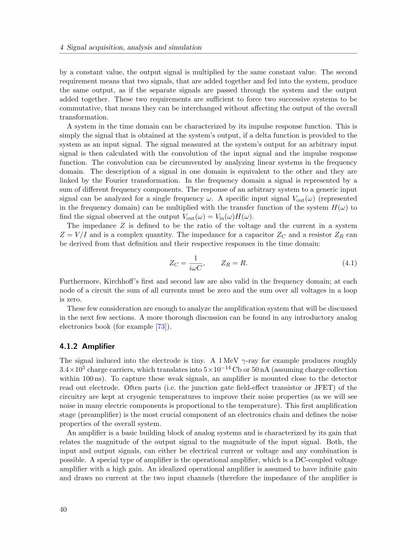
4 Signal acquisition, analysis and simulation
by a constant value, the output signal is multiplied by the same constant value. The secondrequirement means that two signals, that are added together and fed into the system, producethe same output, as if the separate signals are passed through the system and the outputadded together. These two requirements are sufficient to force two successive systems to becommutative, that means they can be interchanged without affecting the output of the overalltransformation.
A system in the time domain can be characterized by its impulse response function. This issimply the signal that is obtained at the system’s output, if a delta function is provided to thesystem as an input signal. The signal measured at the system’s output for an arbitrary inputsignal is then calculated with the convolution of the input signal and the impulse responsefunction. The convolution can be circumvented by analyzing linear systems in the frequencydomain. The description of a signal in one domain is equivalent to the other and they arelinked by the Fourier transformation. In the frequency domain a signal is represented by asum of different frequency components. The response of an arbitrary system to a generic inputsignal can be analyzed for a single frequency ω. A specific input signal Vout(ω) (representedin the frequency domain) can be multiplied with the transfer function of the system H(ω) tofind the signal observed at the output Vout(ω) = Vin(ω)H(ω).
The impedance Z is defined to be the ratio of the voltage and the current in a systemZ = V/I and is a complex quantity. The impedance for a capacitor ZC and a resistor ZR canbe derived from that definition and their respective responses in the time domain:
ZC =1
iωC, ZR = R. (4.1)
Furthermore, Kirchhoff’s first and second law are also valid in the frequency domain; at eachnode of a circuit the sum of all currents must be zero and the sum over all voltages in a loopis zero.
These few consideration are enough to analyze the amplification system that will be discussedin the next few sections. A more thorough discussion can be found in any introductory analogelectronics book (for example [73]).
4.1.2 Amplifier
The signal induced into the electrode is tiny. A 1 MeV γ-ray for example produces roughly3.4×105 charge carriers, which translates into 5×10⁻¹⁴ Cb or 50 nA (assuming charge collectionwithin 100 ns). To capture these weak signals, an amplifier is mounted close to the detectorread out electrode. Often parts (i.e. the junction gate field-effect transistor or JFET) of thecircuitry are kept at cryogenic temperatures to improve their noise properties (as we will seenoise in many electric components is proportional to the temperature). This first amplificationstage (preamplifier) is the most crucial component of an electronics chain and defines the noiseproperties of the overall system.
An amplifier is a basic building block of analog systems and is characterized by its gain thatrelates the magnitude of the output signal to the magnitude of the input signal. Both, theinput and output signals, can either be electrical current or voltage and any combination ispossible. A special type of amplifier is the operational amplifier, which is a DC-coupled voltageamplifier with a high gain. An idealized operational amplifier is assumed to have infinite gainand draws no current at the two input channels (therefore the impedance of the amplifier is
40
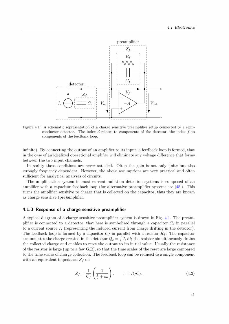
4.1 Electronics
Is Cd
−
+
−A
Rf
Cf
Zf
detector
preamplifier
Zd
Vin Vout
Vf
Figure 4.1: A schematic representation of a charge sensitive preamplifier setup connected to a semi-conductor detector. The index d relates to components of the detector, the index f tocomponents of the feedback loop.
infinite). By connecting the output of an amplifier to its input, a feedback loop is formed, thatin the case of an idealized operational amplifier will eliminate any voltage difference that formsbetween the two input channels.
In reality these conditions are never satisfied. Often the gain is not only finite but alsostrongly frequency dependent. However, the above assumptions are very practical and oftensufficient for analytical analyses of circuits.
The amplification system in most current radiation detection systems is composed of anamplifier with a capacitor feedback loop (for alternative preamplifier systems see [48]). Thisturns the amplifier sensitive to charge that is collected on the capacitor, thus they are knownas charge sensitive (pre)amplifier.
4.1.3 Response of a charge sensitive preamplifier
A typical diagram of a charge sensitive preamplifier system is drawn in Fig. 4.1. The pream-plifier is connected to a detector, that here is symbolized through a capacitor Cd in parallelto a current source Is (representing the induced current from charge drifting in the detector).The feedback loop is formed by a capacitor Cf in parallel with a resistor Rf . The capacitoraccumulates the charge created in the detector Qs =
´Is dt; the resistor simultaneously drains
the collected charge and enables to reset the output to its initial value. Usually the resistanceof the resistor is large (up to a few GΩ), so that the time scales of the reset are large comparedto the time scales of charge collection. The feedback loop can be reduced to a single componentwith an equivalent impedance Zf of:
Zf =1
Cf
(1
1τ + iω
), τ = RfCf . (4.2)
41
4 Signal acquisition, analysis and simulation
In general, all variables in the following discussion are frequency dependent. For betterreadability the frequency dependence, however, is not explicitly mentioned. This also appliesto the transfer function of the operational amplifier A = A(ω), which in all generality candepend on the frequency.
The voltage at the output of the preamplifier is related to the voltage at its input throughVout = −AVin. Furthermore, in Fig. 4.1 it can be seen that Vin = Vf + Vout, thus Vf =(1 +A)Vin. The impedance of an ideal operational amplifier is infinite so no current flows intothe amplifier and the entire current observed at the input of the amplifier (coming from thedetector) flows into the feedback loop If = Iin, thus:
Zin =Vin
Iin=Vin
If=
1
1 +A
VfIf
=ZfA+ 1
. (4.3)
This shows, that the feedback loop can be replaced with an equivalent impedance Zin in parallelto the detector impedance Zd at the input of the amplifier.
If the operational amplifier is near to ideal (A 1 ∀ ω) no current flows into the amplifier.Therefore all the current created in the detectors Is has to flow through the feedback loopand be equal to If . The feedback loop furthermore assures that Vin is close to zero and thusVout = −Vf :
Vout
Is=−VfIf
= −Zf =−1
Cf ( 1τ + iω)
. (4.4)
The transfer function of the system is thus dominated by components of the feedback loop andindependent from the detector capacitance Cd. The transfer functions can be studied in detailby assuming a current signal Is(t) (in the time domain) positioned at t = 0 in the form of adelta function Q0 = δ(t). The time dependence of the charge is then Q(t) =
´Is(t) dt = Q0u(t)
with
u(t) =
0, ∀ t < 0
1, ∀ t ≥ 0(4.5)
being the Heaviside step function. The current signal in the frequency domain Is(ω) = Q0 isfound through a Fourier transformation of the current signal Is(t). The output voltage in thetime domain is then given by:
Vout(t) =
ˆ +∞
−∞
−Q0
Cf ( 1τ + iω)
eiωtdω
2π=−Q0
Cfu(t) e−t/τ (4.6)
This is an Heaviside step function with an exponentially decaying tail defined by the timeconstant τ = RfCf . The rise time of the signal in a radiation detector is chosen to be smallcompared to the decay time, therefore this description is relatively close to real signals observedwith germanium detectors. The gain of the preamplifier system G = 1/Cf is controlled solelyby the feedback capacitance. Accordingly a small value for the feedback capacitance must bechosen to maximize the output signal. Investigating Eq. 4.4 in more detail, it can be observed,that for the approximation to be true not only the gain of the amplifier A must be large,but also Cd/A Cf ∀ ω. Thus for a finite gain of the operational preamplifier it must beassured that the capacitance of the detector is small enough compared to the capacitance ofthe feedback loop, such that this inequality is valid.
42
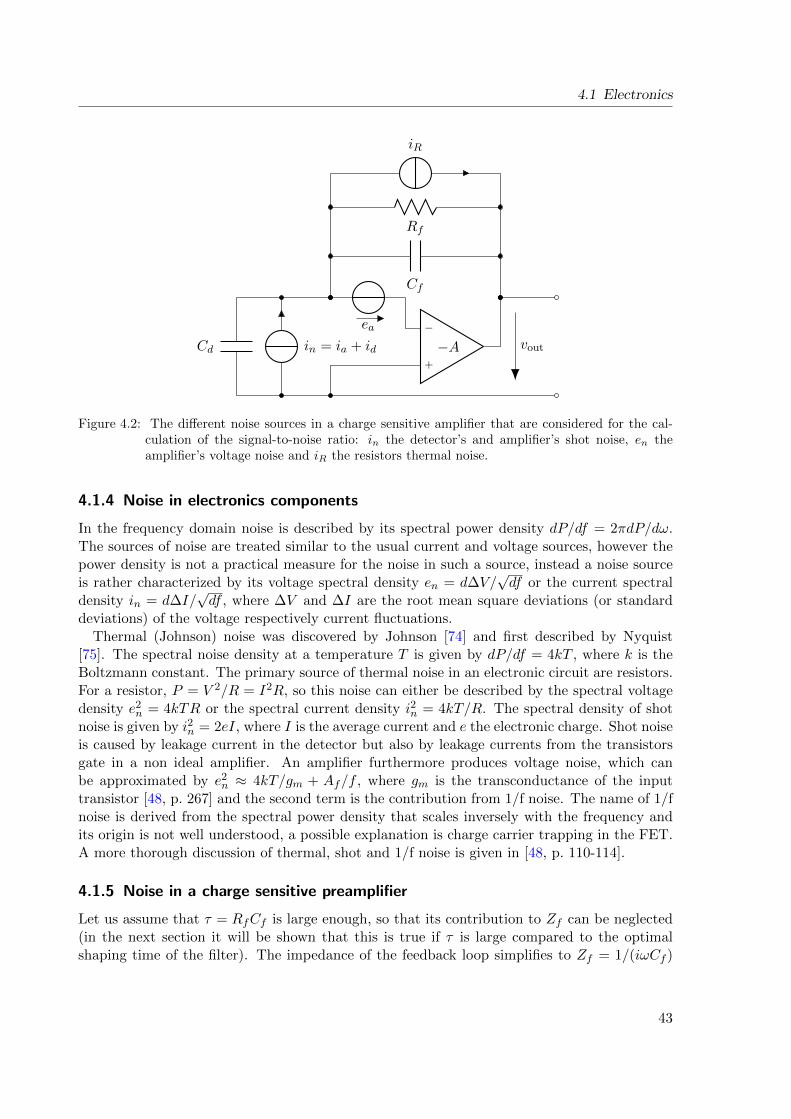
4.1 Electronics
Cd in = ia + id
−
+
−Aea
Rf
iR
Cf
vout
Figure 4.2: The different noise sources in a charge sensitive amplifier that are considered for the cal-culation of the signal-to-noise ratio: in the detector’s and amplifier’s shot noise, en theamplifier’s voltage noise and iR the resistors thermal noise.
4.1.4 Noise in electronics components
In the frequency domain noise is described by its spectral power density dP/df = 2πdP/dω.The sources of noise are treated similar to the usual current and voltage sources, however thepower density is not a practical measure for the noise in such a source, instead a noise sourceis rather characterized by its voltage spectral density en = d∆V/
√df or the current spectral
density in = d∆I/√df , where ∆V and ∆I are the root mean square deviations (or standard
deviations) of the voltage respectively current fluctuations.Thermal (Johnson) noise was discovered by Johnson [74] and first described by Nyquist
[75]. The spectral noise density at a temperature T is given by dP/df = 4kT , where k is theBoltzmann constant. The primary source of thermal noise in an electronic circuit are resistors.For a resistor, P = V 2/R = I2R, so this noise can either be described by the spectral voltagedensity e2
n = 4kTR or the spectral current density i2n = 4kT/R. The spectral density of shotnoise is given by i2n = 2eI, where I is the average current and e the electronic charge. Shot noiseis caused by leakage current in the detector but also by leakage currents from the transistorsgate in a non ideal amplifier. An amplifier furthermore produces voltage noise, which canbe approximated by e2
n ≈ 4kT/gm + Af/f , where gm is the transconductance of the inputtransistor [48, p. 267] and the second term is the contribution from 1/f noise. The name of 1/fnoise is derived from the spectral power density that scales inversely with the frequency andits origin is not well understood, a possible explanation is charge carrier trapping in the FET.A more thorough discussion of thermal, shot and 1/f noise is given in [48, p. 110-114].
4.1.5 Noise in a charge sensitive preamplifier
Let us assume that τ = RfCf is large enough, so that its contribution to Zf can be neglected(in the next section it will be shown that this is true if τ is large compared to the optimalshaping time of the filter). The impedance of the feedback loop simplifies to Zf = 1/(iωCf )
43
4 Signal acquisition, analysis and simulation
and as before, the impedance of the detector is given by Zd = 1/(iωCd). Furthermore, let usconsider the three noise sources shown in Fig. 4.2:
i2n = i2a + i2d = 2e(IG + IL), (4.7)
i2R = 4kT/Rf , (4.8)
e2a =
8kT
3gm+
2πAfω
. (4.9)
The voltage noise of the preamplifier ea contains the 1/f noise (reminder: 2πf = ω) and thecontribution from the amplifier is expressed with the transconductance gm. iR is the thermalnoise of the feedback resistor and in the shot noise created by the detector leakage current ILand the transistor gate leakage current IG. These noise sources were chosen according to [76],other text discussing the issue might include different noise sources according to their needs.An actual charge sensitive preamplifier is composed of many more components that each mayor may not add noise, however for the purpose of this discussions the three mentioned noisesources are sufficient.
The noise sources are independent from each other, so the contribution of each noise sourceobserved at the output of the preamplifier can be calculated separately, however the transferfunction of the system to each individual noise source must be considered. The total noise atthe output of the preamplifier is found by adding all the different contributions from individualsources in quadrature.
Considering only the source ea, the two impedances act as a capacitor divider therefore thenoise at the output vout for this source is:
vout,e = en + Vf = en + enZfZd
= (1 +CdCf
)en. (4.10)
In the derivation of this equation the voltage drop over the input was assumed to be zero,which is valid for an ideal operational amplifier.
Considering now only the two current sources in and iR. It can be shown, that the transferfunction of the system has the same impact onto these two sources. Therefore, their contribu-tion at the output of the preamplifier is:
vout,n = inZf =in
iωCf, vout,R = iRZf =
iRiωCf
. (4.11)
These three contribution are added in quadrature and the exact expression of the spectral noisedensities can be inserted to find the total spectral noise density at the output of the amplifier:
v2out =
8kT
3gm
(1 +
CdCf
)2
+2πAfω
(1 +
CdCf
)2
+1
C2fω
2
(2e(IG + IL) +
4kT
Rf
). (4.12)
This expression contains three terms, one constant, one proportional to 1/ω and one propor-tional to 1/ω2. Furthermore, the detector capacitance Cd also appears in the expression. Thisis in contrast to the signal at the preamplifier output which only depended on the feedbackcapacitance Cf (see Eq. 4.6). Its appearance in Eq. 4.12 is solely caused by the voltage noise ofthe amplifier. Finally, the noise sources depend on the feedback resistance Rf and the leakagecurrents IL and IG, so they also add to the observed noise at the output of the preamplifierstage.
44
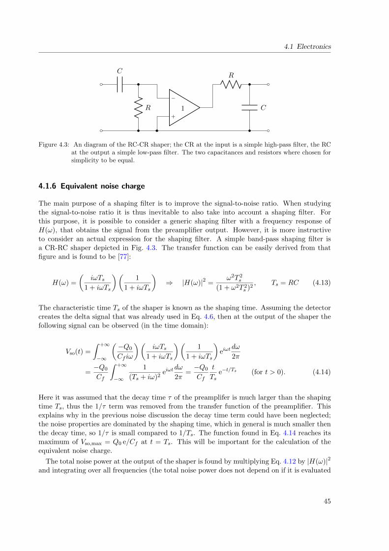
4.1 Electronics
−
+
1
CR
R C
Figure 4.3: An diagram of the RC-CR shaper; the CR at the input is a simple high-pass filter, the RCat the output a simple low-pass filter. The two capacitances and resistors where chosen forsimplicity to be equal.
4.1.6 Equivalent noise charge
The main purpose of a shaping filter is to improve the signal-to-noise ratio. When studyingthe signal-to-noise ratio it is thus inevitable to also take into account a shaping filter. Forthis purpose, it is possible to consider a generic shaping filter with a frequency response ofH(ω), that obtains the signal from the preamplifier output. However, it is more instructiveto consider an actual expression for the shaping filter. A simple band-pass shaping filter isa CR-RC shaper depicted in Fig. 4.3. The transfer function can be easily derived from thatfigure and is found to be [77]:
H(ω) =
(iωTs
1 + iωTs
)(1
1 + iωTs
)⇒ |H(ω)|2 =
ω2T 2s
(1 + ω2T 2s )2
, Ts = RC (4.13)
The characteristic time Ts of the shaper is known as the shaping time. Assuming the detectorcreates the delta signal that was already used in Eq. 4.6, then at the output of the shaper thefollowing signal can be observed (in the time domain):
Vso(t) =
ˆ +∞
−∞
(−Q0
Cf iω
)(iωTs
1 + iωTs
)(1
1 + iωTs
)eiωt
dω
2π
=−Q0
Cf
ˆ +∞
−∞
1
(Ts + iω)2eiωt
dω
2π=−Q0
Cf
t
Tse−t/Ts (for t > 0). (4.14)
Here it was assumed that the decay time τ of the preamplifer is much larger than the shapingtime Ts, thus the 1/τ term was removed from the transfer function of the preamplifier. Thisexplains why in the previous noise discussion the decay time term could have been neglected;the noise properties are dominated by the shaping time, which in general is much smaller thenthe decay time, so 1/τ is small compared to 1/Ts. The function found in Eq. 4.14 reaches itsmaximum of Vso,max = Q0 e/Cf at t = Ts. This will be important for the calculation of theequivalent noise charge.
The total noise power at the output of the shaper is found by multiplying Eq. 4.12 by |H(ω)|2and integrating over all frequencies (the total noise power does not depend on if it is evaluated
45
4 Signal acquisition, analysis and simulation
in the time or frequency domain):
v2so =
8kT
3gm
(1 +
CdCf
)2 ˆ ∞0|H(ω)|2 dω
2π
+ 2πAf
(1 +
CdCf
)2 ˆ ∞0
|H(ω)|2
ω
dω
2π
+1
C2f
(2e(IG + IL) +
4kT
Rf
) ˆ ∞0
|H(ω)|2
ω2
dω
2π. (4.15)
The transfer function in Eq. 4.15 can be replaced with the actual expression for the CR-RCshaper, which leads to three integrals that can be evaluated with the identity:
ˆ ∞0
ωm dω
(ωn + an)r=
(−1)r−1πam+1−nrΓ[(m+ 1)/n]
n sin[(m+ 1)π/n](r − 1)!Γ[(m+ 1)/n− r + 1], (4.16)
where a = 1/Ts and r = n = 2. The total noise at the output of the shaping filter is thusfound to be:
v2so =
8kT
3gm
(1 +
CdCf
)2 1
8Ts+ 2πAf
(1 +
CdCf
)2 1
4π+
1
C2f
(2e(IG + IL) +
4kT
Rf
)Ts8
. (4.17)
The equivalent noise charge is given by the relation:
Qn = Q0/(S/N), (4.18)
where Q0 is the magnitude of the signal at the input to the preamplifier stage and (S/N) thesignal-to-noise ratio observed at the output of the shaping filter for that very signal. Accord-ingly, it expresses the noise level that is observed at the output of the shaping filter in unitsof the input signal to the preamplification stage (i.e. number of charged particles, Coulombor eV). As the magnitude appears twice in the above expression (first in the definition of Q0
and then in the signal-to-noise ratio) the equivalent noise charge is independent of the signalheight and only expresses the actual noise level of a system. In the case of the CR-RC shaperwe thus find for the equivalent noise charge squared:
Q2n = Q2
0
v2so
V 2so,max
=e2
8
[8kT
3gm
C2t
Ts+ 4AfC
2t +
(2e(IG + IL) +
4kT
Rf
)Ts
](4.19)
In this equation Ct = Cf +Cd is the sum of the capacitances in the system and e2 is the Eulernumber squared. The equivalent noise charge has therefore three terms, one is proportional toTs one is independent of Ts and one is inversely proportional to Ts. A similar result is foundfor other shapers, thus the equivalent noise is in general expressed as:
Q2n = i2nFiTs + e2
nFeC2
Ts+ FfAfC
2, (4.20)
where for universal validity the current noise sources are combined to in and the voltage noisesources are combined to en. The time constant Ts is defined by the respective shaping filterand its definition is not unique. The shaping factors Fi, Fv and Ff are constants and found by
46
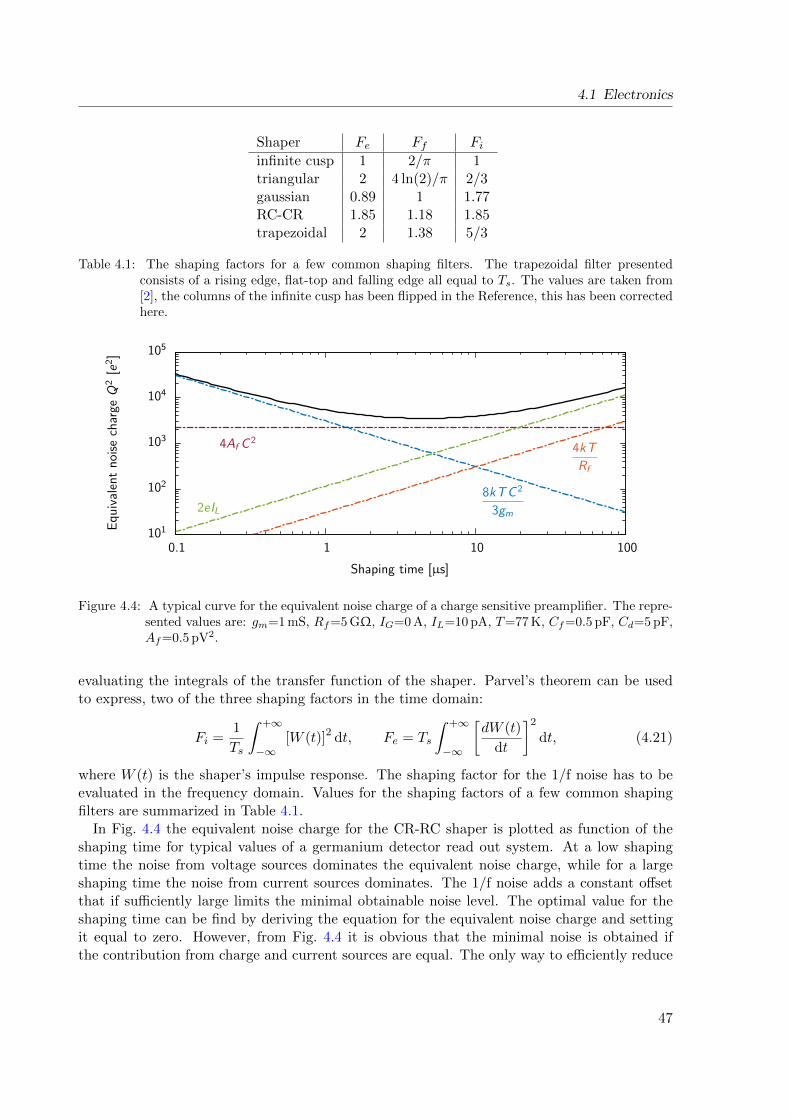
4.1 Electronics
Shaper Fe Ff Fiinfinite cusp 1 2/π 1triangular 2 4 ln(2)/π 2/3gaussian 0.89 1 1.77RC-CR 1.85 1.18 1.85trapezoidal 2 1.38 5/3
Table 4.1: The shaping factors for a few common shaping filters. The trapezoidal filter presentedconsists of a rising edge, flat-top and falling edge all equal to Ts. The values are taken from[2], the columns of the infinite cusp has been flipped in the Reference, this has been correctedhere.
101
102
103
104
105
0.1 1 10 100
Eq
uiv
alen
tn
oise
char
geQ
2[e
2]
Shaping time [µs]
8kTC 2
3gm
4Af C2
2eIL
4kT
Rf
Figure 4.4: A typical curve for the equivalent noise charge of a charge sensitive preamplifier. The repre-sented values are: gm=1 mS, Rf=5 GΩ, IG=0 A, IL=10 pA, T=77 K, Cf=0.5 pF, Cd=5 pF,Af=0.5 pV2.
evaluating the integrals of the transfer function of the shaper. Parvel’s theorem can be usedto express, two of the three shaping factors in the time domain:
Fi =1
Ts
ˆ +∞
−∞[W (t)]2 dt, Fe = Ts
ˆ +∞
−∞
[dW (t)
dt
]2
dt, (4.21)
where W (t) is the shaper’s impulse response. The shaping factor for the 1/f noise has to beevaluated in the frequency domain. Values for the shaping factors of a few common shapingfilters are summarized in Table 4.1.
In Fig. 4.4 the equivalent noise charge for the CR-RC shaper is plotted as function of theshaping time for typical values of a germanium detector read out system. At a low shapingtime the noise from voltage sources dominates the equivalent noise charge, while for a largeshaping time the noise from current sources dominates. The 1/f noise adds a constant offsetthat if sufficiently large limits the minimal obtainable noise level. The optimal value for theshaping time can be find by deriving the equation for the equivalent noise charge and settingit equal to zero. However, from Fig. 4.4 it is obvious that the minimal noise is obtained ifthe contribution from charge and current sources are equal. The only way to efficiently reduce
47
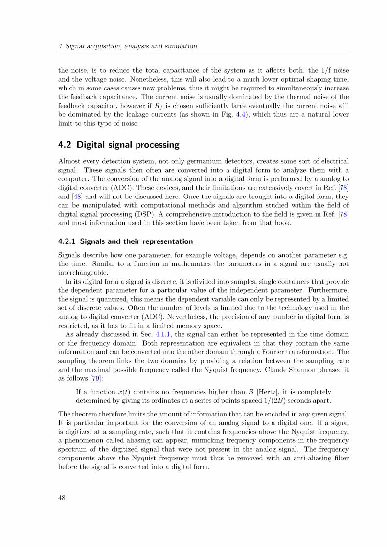
4 Signal acquisition, analysis and simulation
the noise, is to reduce the total capacitance of the system as it affects both, the 1/f noiseand the voltage noise. Nonetheless, this will also lead to a much lower optimal shaping time,which in some cases causes new problems, thus it might be required to simultaneously increasethe feedback capacitance. The current noise is usually dominated by the thermal noise of thefeedback capacitor, however if Rf is chosen sufficiently large eventually the current noise willbe dominated by the leakage currents (as shown in Fig. 4.4), which thus are a natural lowerlimit to this type of noise.
4.2 Digital signal processing
Almost every detection system, not only germanium detectors, creates some sort of electricalsignal. These signals then often are converted into a digital form to analyze them with acomputer. The conversion of the analog signal into a digital form is performed by a analog todigital converter (ADC). These devices, and their limitations are extensively covert in Ref. [78]and [48] and will not be discussed here. Once the signals are brought into a digital form, theycan be manipulated with computational methods and algorithm studied within the field ofdigital signal processing (DSP). A comprehensive introduction to the field is given in Ref. [78]and most information used in this section have been taken from that book.
4.2.1 Signals and their representation
Signals describe how one parameter, for example voltage, depends on another parameter e.g.the time. Similar to a function in mathematics the parameters in a signal are usually notinterchangeable.
In its digital form a signal is discrete, it is divided into samples, single containers that providethe dependent parameter for a particular value of the independent parameter. Furthermore,the signal is quantized, this means the dependent variable can only be represented by a limitedset of discrete values. Often the number of levels is limited due to the technology used in theanalog to digital converter (ADC). Nevertheless, the precision of any number in digital form isrestricted, as it has to fit in a limited memory space.
As already discussed in Sec. 4.1.1, the signal can either be represented in the time domainor the frequency domain. Both representation are equivalent in that they contain the sameinformation and can be converted into the other domain through a Fourier transformation. Thesampling theorem links the two domains by providing a relation between the sampling rateand the maximal possible frequency called the Nyquist frequency. Claude Shannon phrased itas follows [79]:
If a function x(t) contains no frequencies higher than B [Hertz], it is completelydetermined by giving its ordinates at a series of points spaced 1/(2B) seconds apart.
The theorem therefore limits the amount of information that can be encoded in any given signal.It is particular important for the conversion of an analog signal to a digital one. If a signalis digitized at a sampling rate, such that it contains frequencies above the Nyquist frequency,a phenomenon called aliasing can appear, mimicking frequency components in the frequencyspectrum of the digitized signal that were not present in the analog signal. The frequencycomponents above the Nyquist frequency must thus be removed with an anti-aliasing filterbefore the signal is converted into a digital form.
48
4.2 Digital signal processing
4.2.2 Digital linear systems
Digital filters are digital linear systems and follow the definition given in Sec. 4.1.1 for theiranalog counterparts. In the time domain, these systems are characterized by the impulseresponse h, that allows to calculate for any input signal x the output signal y, by performing aconvolution of the input signal with the impulse response (we only consider the discrete formof a convolution):
y[i] =
M∑j=0
h[j]x[i− j]. (4.22)
Although, the convolution is sufficient to calculate any response for a given input signal, it ismore practical to calculate a systems response with the recursive formula:
y[i] =
i∑j=0
ajx[i− j] +
i∑j=0
bjy[i− j]. (4.23)
This form not only includes the input signal but also uses the output signal calculated forproceeding samples. This expression contains the recursion coefficients aj and bj which definethe system completely.
The most fundamental filters are the single pole low-pass, single pole high-pass and themoving average filter. Their non-zero recursive coefficients are:
• Low-pass filter: a0 = 1− d, b1 = d,
• high-pass filter: a0 = (1 + d)/2, a1 = −(1 + d)/2, b1 = d,
• moving average filter: a0 = 1, ap = −1 , b0 = 1.
The parameter d, defines the decay on a sample basis and is related to the decay time τ bythe relation d = e−1/τ . The parameter p indicates the number of samples (length) that areaveraged in the moving average. The analog version of the low-pass filter and high-pass filterhave been previously encountered in Sec. 4.1.6 as the CR segment (low-pass filter) and the RCsegment (high-pass filter).
Shaping filters change the form of the input pulse into a form that has a better signal-to-noiseration. Thus, their main purpose is to remove undesired regions in the frequency domain.Theabove listed filters are not particular well suited as shaping filters, as in the frequency domaintheir response function stretches over a relative large range of frequencies. Nonetheless, theperformance can be improved by applying a sequence of filters, one after the other.
The shaping time is the characteristic parameter of these filters and has been emergingnaturally from the discussion in Sec. 4.1.6. There are different ways of defining it. Sometimes,the shaping time is the width of the moving window average filters, but more often it is thewidth of the shaped signal. In this thesis the shaping time Ts is defined to be the full-width-at-half-maximum (FWHM) of the shaped signal and it is related to the length of the movingaverage filter p by p =
√2Ts.
The most popular shaping filter in radiation detection systems is composed of consecutivemoving average filters of the same width. After the first moving average filter the impulseresponse has the shape of a rectangular function, after the second moving average filter ittakes the form of a triangular function and then approaches with each further stage a Gaussian
49
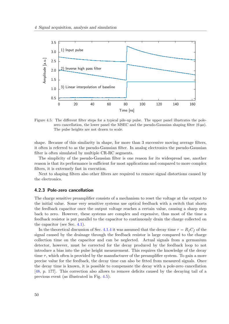
4 Signal acquisition, analysis and simulation
0.5
1.0
1.5
2.0
2.5
3.0
3.5
0 20 40 60 80 100 120 140 160
Am
plit
ud
e[a
.u.]
Time [ns]
1) Input pulse
2) Inverse high pass filter
3) Linear interpolation of baseline
Figure 4.5: The different filter steps for a typical pile-up pulse. The upper panel illustrates the pole-zero cancellation, the lower panel the MSEC and the pseudo-Gaussian shaping filter (6µs).The pulse heights are not drawn to scale.
shape. Because of this similarity in shape, for more than 3 successive moving average filters,it often is referred to as the pseudo-Gaussian filter. In analog electronics the pseudo-Gaussianfilter is often simulated by multiple CR-RC segments.
The simplicity of the pseudo-Gaussian filter is one reason for its widespread use, anotherreason is that its performance is sufficient for most applications and compared to more complexfilters, it is extremely fast in execution.
Next to shaping filters also other filters are required to remove signal distortions caused bythe electronics.
4.2.3 Pole-zero cancellation
The charge sensitive preamplifier consists of a mechanism to reset the voltage at the output tothe initial value. Some very sensitive systems use optical feedback with a switch that shortsthe feedback capacitor once the output voltage reaches a certain value, causing a sharp stepback to zero. However, these systems are complex and expensive, thus most of the time afeedback resistor is put parallel to the capacitor to continuously drain the charge collected onthe capacitor (see Sec. 4.1).
In the theoretical discussion of Sec. 4.1.4 it was assumed that the decay time τ = RfCf of thesignal caused by the drainage through the feedback resistor is large compared to the chargecollection time on the capacitor and can be neglected. Actual signals from a germaniumdetector, however, must be corrected for the decay produced by the feedback loop to notintroduce a bias into the pulse height measurement. This requires the knowledge of the decaytime τ , which often is provided by the manufacturer of the preamplifier system. To gain a moreprecise value for the feedback, the decay time can also be fitted from measured signals. Oncethe decay time is known, it is possible to compensate the decay with a pole-zero cancellation[48, p. 177]. This correction also allows to remove deficits caused by the decaying tail of aprevious event (as illustrated in Fig. 4.5).
50
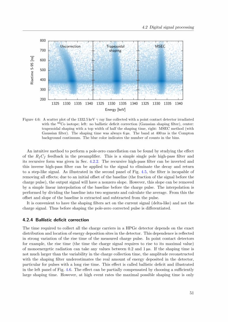
4.2 Digital signal processingR
iset
ime
5-95
[ns]
Energy [keV]
200
300
400
500
600
700
800
1325 1330 1335 1340
Uncorrection
1325 1330 1335 1340
Trapezoidalshaping
1325 1330 1335 1340
MSEC
Figure 4.6: A scatter plot of the 1332.5 keV γ ray line collected with a point contact detector irradiatedwith the 60Co isotope; left: no ballistic deficit correction (Gaussian shaping filter), center:trapezoidal shaping with a top width of half the shaping time, right: MSEC method (withGaussian filter). The shaping time was always 6µs. The band at 400 ns is the Comptonbackground continuum. The blue color indicates the number of counts in the bins.
An intuitive method to perform a pole-zero cancellation can be found by studying the effectof the RfCf feedback in the preamplifier. This is a simple single pole high-pass filter andits recursive form was given in Sec. 4.2.2. The recursive high-pass filter can be inverted andthis inverse high-pass filter can be applied to the signal to eliminate the decay and returnto a step-like signal. As illustrated in the second panel of Fig. 4.5, the filter is incapable ofremoving all effects; due to an initial offset of the baseline (the fraction of the signal before thecharge pulse), the output signal will have a nonzero slope. However, this slope can be removedby a simple linear interpolation of the baseline before the charge pulse. The interpolation isperformed by dividing the baseline into two segments and calculate the average. From this theoffset and slope of the baseline is extracted and subtracted from the pulse.
It is convenient to have the shaping filters act on the current signal (delta-like) and not thecharge signal. Thus before shaping the pole-zero corrected pulse is differentiated.
4.2.4 Ballistic deficit correction
The time required to collect all the charge carriers in a HPGe detector depends on the exactdistribution and location of energy deposition sites in the detector. This dependence is reflectedin strong variation of the rise time of the measured charge pulse. In point contact detectorsfor example, the rise time (the time the charge signal requires to rise to its maximal value)of monoenergetic radiation can take any values between 0.2 and 1µs. If the shaping time isnot much larger than the variability in the charge collection time, the amplitude reconstructedwith the shaping filter underestimates the real amount of energy deposited in the detector,particular for pulses with a long rise time. This effect is called ballistic deficit and illustratedin the left panel of Fig. 4.6. The effect can be partially compensated by choosing a sufficientlylarge shaping time. However, at high event rates the maximal possible shaping time is only
51

4 Signal acquisition, analysis and simulation
0
2000
4000
6000
8000
10000
1328 1330 1332 1334 1336
Cou
nts
Energy [keV]
Uncorrected: FWHM 1.820± 0.012 keVTrapezoidal: FWHM 1.623± 0.007 keV
MSEC: FWHM 1.611± 0.007 keV
Figure 4.7: A histogram of the 1332.5 keV γ ray line represented in Fig. 4.6; for no ballistic deficitcorrection, a trapezoidal shaping with a top width of half the shaping time, and MSECmethod enabled. The shaping time was always 6µs. The improvement of any of the twoballistic deficit corrections with respect to the uncorrected analysis is roughly 10-11%.
a few microseconds, which is not sufficiently large to remove all effects caused by the ballisticdeficit.
In the past, three different approaches were proposed to correct ballistic deficits, whichmostly relayed on analog electronics. The first approach calculated a semi-empirical compen-sation which depended on the input signal rise time and then was added to the final outputsignal [80]. The second approach used a gated integrator after prefiltering the signal to in-tegrate over the charge carrier drift time [81]. The third approach is to choose a particularshaping filter, that convert the input signal into a trapezoidal form [82]. This filter is wellsuited for correcting ballistic deficit effects but not optimal to minimize the signal-to-noiseratio of the pulse height reconstruction. Implementing a correction with digital methods ismuch simpler than with analog circuits, but usually follows the same principles.
The classical trapezoidal filter is made up of two moving average filters with different shapingtimes. The length of the longer moving average filter defines the shaping time of the trapezoidalfilter, the length of the shorter moving average filter defines the width of the flat-top part ofthe trapezoidal form. The flat-top part must be chosen sufficiently large to compensate for thevariability in the rise time, but should not be too large as it weights noise contribution toohigh. The amplitude of the shaped signal must be measured at a fixed position of the shapedsignal, best towards the end of the flat-top part to be less sensitive to rise time variations. Analternative approach has been chosen in this thesis by applying an additional moving averagefilter to alter the top into a round shape and create a clear maximum. This method slightlyreduces the filters efficiency to compensate ballistic deficits, however it is much easier to definethe pulse height value. In the central panel of Fig. 4.6 this rounded-top trapezoidal filter wasused. It shows that the filter still is capable of compensating ballistic deficits.
52
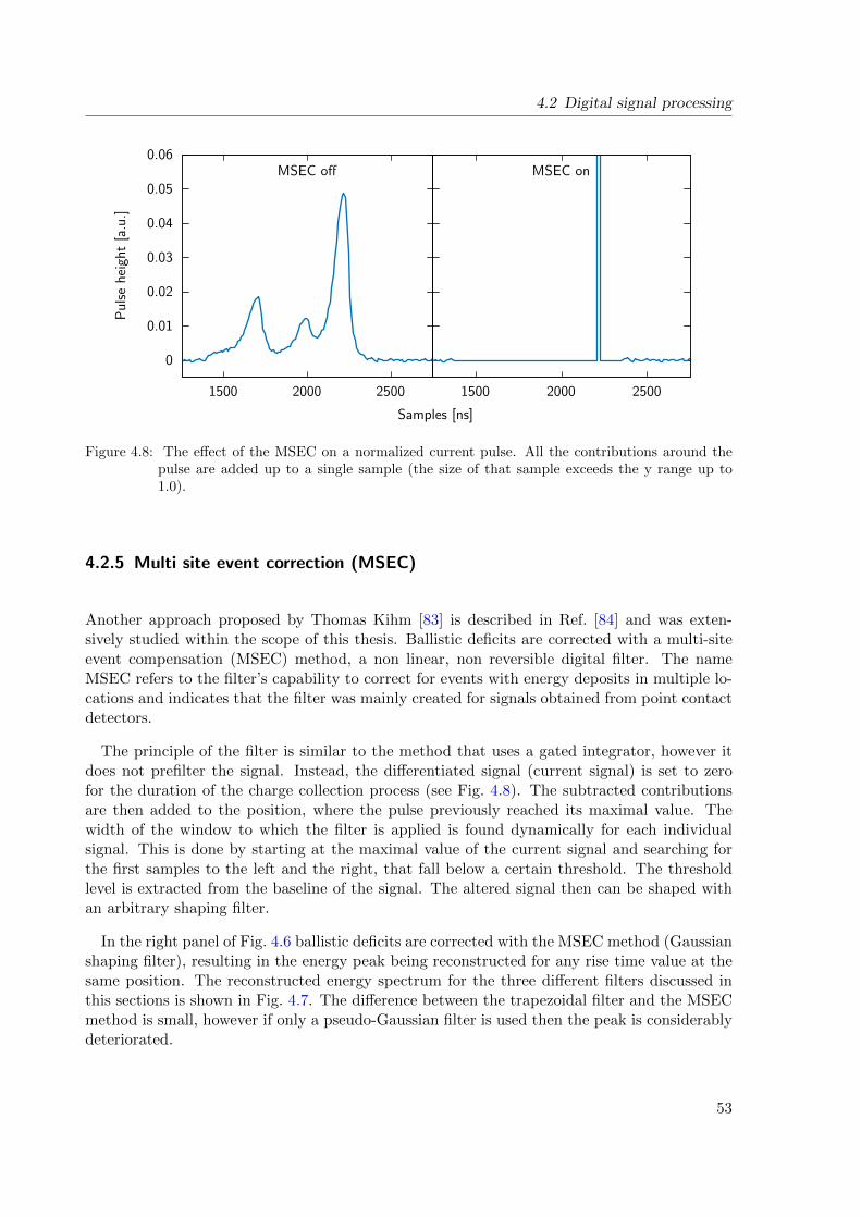
4.2 Digital signal processing
0
0.01
0.02
0.03
0.04
0.05
0.06
1500 2000 2500
Pu
lse
hei
ght
[a.u
.]
1500 2000 2500
MSEC off
Samples [ns]
MSEC on
Figure 4.8: The effect of the MSEC on a normalized current pulse. All the contributions around thepulse are added up to a single sample (the size of that sample exceeds the y range up to1.0).
4.2.5 Multi site event correction (MSEC)
Another approach proposed by Thomas Kihm [83] is described in Ref. [84] and was exten-sively studied within the scope of this thesis. Ballistic deficits are corrected with a multi-siteevent compensation (MSEC) method, a non linear, non reversible digital filter. The nameMSEC refers to the filter’s capability to correct for events with energy deposits in multiple lo-cations and indicates that the filter was mainly created for signals obtained from point contactdetectors.
The principle of the filter is similar to the method that uses a gated integrator, however itdoes not prefilter the signal. Instead, the differentiated signal (current signal) is set to zerofor the duration of the charge collection process (see Fig. 4.8). The subtracted contributionsare then added to the position, where the pulse previously reached its maximal value. Thewidth of the window to which the filter is applied is found dynamically for each individualsignal. This is done by starting at the maximal value of the current signal and searching forthe first samples to the left and the right, that fall below a certain threshold. The thresholdlevel is extracted from the baseline of the signal. The altered signal then can be shaped withan arbitrary shaping filter.
In the right panel of Fig. 4.6 ballistic deficits are corrected with the MSEC method (Gaussianshaping filter), resulting in the energy peak being reconstructed for any rise time value at thesame position. The reconstructed energy spectrum for the three different filters discussed inthis sections is shown in Fig. 4.7. The difference between the trapezoidal filter and the MSECmethod is small, however if only a pseudo-Gaussian filter is used then the peak is considerablydeteriorated.
53
4 Signal acquisition, analysis and simulation
4.2.6 Optimal filtering
The Wiener filter theory, established by Norbert Wiener in 1949 [85], describes a simple methodto find the best filter for a given frequency distribution of the signal and the noise. A simpleversion of his theory states, that the optimal filter response is given by [78]:
H(ω) =S(ω)2
S(ω)2 +N(ω)2, (4.24)
where S(ω) is the signal and N(ω) the noise distribution in the frequency domain. The equationdefines the shaping function to weight each frequency by the amount of signal relative to thesum of the signal and the noise. The definition requires the explicit knowledge of the entirenoise and signal frequency spectra, which usually is not given. Moreover, the equation leadsto a non-causal infinite pulse response in the time domain, which is unpractical for any realapplication. It is possible to find an alternative definition of the above equation, that forbidsnon-causal and infinite solutions but for a short theoretical study the above form is sufficient.
The signal and noise at the output of a typical charge sensitive preamplifier in the frequencydomain was calculated in Sec. 4.1. The signal was found to be Vout(ω)2 = Q2
0/(ω2C2
f ) = A/ω2,where the preamplifier decay time was assumed to be large enough so that its contributioncan be neglected. The noise was obtained in Eq. 4.12 and can be reduced to the form v2
out =B + C/ω2, where the contribution from 1/f noise was neglected. Thus the optimal shapingfilter in the frequency domain is given by:
H(ω) =A/ω2
A/ω2 + (B + C/ω2)=
A
2τB
(2τ
τ2 + ω2
), τ2 =
A+ C
B. (4.25)
The entire frequency dependence is collected in the second factor. This expression has a simpleknown equation for the corresponding signal in the time domain: A two sided exponential. Thusthe impulse response of the filter in the time domain is given by:
H(t) =A
2τBe−|t|/τ . (4.26)
This is the form of the so called cusp filter and as shown in its derivation it provides thebest signal-to-noise ratio for a input delta signal and a system that is free of 1/f noise. Theexponentially decaying tails of the cusp filter imply that the impulse response stretches toinfinity, which is not practical in an actual analysis as data are only available in a very confinedrange. The loss in resolution, however, is small if the signal is cut of at a few decay times distanton each side. The cusp filter used within this thesis has been cut off at 5 times the decay timeon each side.
In the analog to digital conversion a sufficiently large range around the signal is storedto disk and thus the filter can also make use of information that would be inaccessible inanalog electronics as they happen in the future. This can be used to synthesize the cusp filteroffline with simple recursive methods; the recursive form of the cusp filter is composed of twobidirectional low-pass filters.
The form of the cusp filter’s impulse response has a very sharp peak at its maximum. Asdiscussed in the previous sections such a impulse response is not capable of correcting ballisticdeficits. The sharp peak of the classical cusp filter thus has been flattened with an additionalmoving window average within the scope of this thesis. This creates a cusp like form with a
54
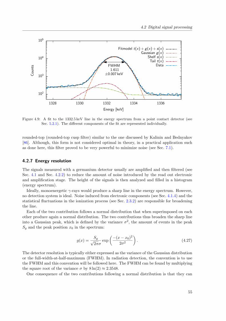
4.2 Digital signal processing
102
103
104
105
1328 1330 1332 1334 1336
Cou
nts
Energy [keV]
DataTail t(x)
Shelf s(x)Gaussian g(x)
Fitmodel t(x) + g(x) + s(x)
FWHM1.611
±0.007 keV
Figure 4.9: A fit to the 1332.5 keV line in the energy spectrum from a point contact detector (seeSec. 5.2.1). The different components of the fit are represented individually.
rounded-top (rounded-top cusp filter) similar to the one discussed by Kalinin and Bednyakov[86]. Although, this form is not considered optimal in theory, in a practical application suchas done here, this filter proved to be very powerful to minimize noise (see Sec. 7.1).
4.2.7 Energy resolution
The signals measured with a germanium detector usually are amplified and then filtered (seeSec. 4.1 and Sec. 4.2.2) to reduce the amount of noise introduced by the read out electronicand amplification stage. The height of the signals is then analyzed and filled in a histogram(energy spectrum).
Ideally, monoenergetic γ-rays would produce a sharp line in the energy spectrum. However,no detection system is ideal. Noise induced from electronic components (see Sec. 4.1.4) and thestatistical fluctuations in the ionization process (see Sec. 2.3.2) are responsible for broadeningthe line.
Each of the two contribution follows a normal distribution that when superimposed on eachother produce again a normal distribution. The two contributions thus broaden the sharp lineinto a Gaussian peak, which is defined by the variance σ2, the amount of events in the peakSg and the peak position x0 in the spectrum:
g(x) =Sg√2πσ
exp
(−(x− x0)2
2σ2
). (4.27)
The detector resolution is typically either expressed as the variance of the Gaussian distributionor the full-width-at-half-maximum (FWHM). In radiation detection, the convention is to usethe FWHM and this convention will be followed here. The FWHM can be found by multiplyingthe square root of the variance σ by 8 ln(2) ≈ 2.3548.
One consequence of the two contributions following a normal distribution is that they can
55
4 Signal acquisition, analysis and simulation
be added in quadrature to calculate the total variance σ2T :
σ2T = σ2
S + σ2E = FεE + ε2Q2
n. (4.28)
The contribution from statistical fluctuations σ2S is proportional to the Fano factor F and the
energy of the incident radiation particle E. The average energy required to create an electron-hole-pair ε is used to convert a number of electrons to units of energy. Thus the contributionfrom electronics noise σ2
N is found from the equivalent noise charge Qn, that usually is expressedas the number of electrons that correspond to the average noise in the system and which isindependent from the energy of the radiation. The noise resolution and the equivalent noisecharge are thus identical (up to a conversion constant) and will be used as synonyms.
In reality, there are additional effects that distort the shape of a typical energy peak. Thesecontributions usually do not follow a normal distribution and should not be added in quadra-ture. The most important distortion is caused by charge trapping in the detector. As discussedbriefly in Sec. 2.2.2, trapping sites can capture some of the charge carriers and either absorbthem or release them with a certain delay. The typical time a charge carrier is trapped in such asite follows an exponentially decaying distribution. Depending on the strength of trapping, theevents are reconstructed at slightly lower energies. Counts are removed from the peak formingan exponentially decaying distribution below the main peak [87]. However, this feature is alsobroadened by the electronics noise and charge carrier statistics – the actual form of the lowenergetic tail can be described by a convolution of the exponentially decaying distribution witha Gaussian function [88]:
t(x) =St2β
exp
(x− x0
β+
σ2
2β2
)· erfc
(x− x0√
2σ+
σ√2β
). (4.29)
In this equation, often referred to as the Hypermet function, β is the decay constant of theexponentially decaying distribution, σ and x0 are the parameters defining the Gaussian broad-ening and St is the number of counts in the peak. The Hypermet function was not correctlynormalized in Ref. [88], however it is corrected here. The Hypermet function is also referredto as exponentially modified Gaussian (EMG) and for example used in Chromatography forpeak reconstruction [89].
This distortion of the peak can be large enough so that it must be taken into account forcalculating the detector resolution. This leads to an ambiguity in the definition of the detectorresolution. If one is only interested how precisely the initial γ-ray energy can be reconstructed,then the FWHM is calculated including this additional distribution. On the other hand, ifone is interested in material characteristics such as the Fano factor, then the tails must besubtracted to gain a unbiased value of the variance of the distribution. For most of this thesis,the detector resolution will be provided as a FWHM value that includes the spread throughthe tailing term. When calculating the Fano factor the resolution will be given as the varianceσ of the Gaussian distribution only.
The distortion needs to be also considered when measuring the number of events in a peak.In that situation the contribution from the tail and the Gaussian must be added Stot = St+Sg.
It is rarely the case, that a peak is background free. Particularly, Compton scattered eventcreate a continuum underneath the peak. Ideally, this background component is a step functionwith a constant offset, but also this distribution is broadened, resulting in a function falling
56
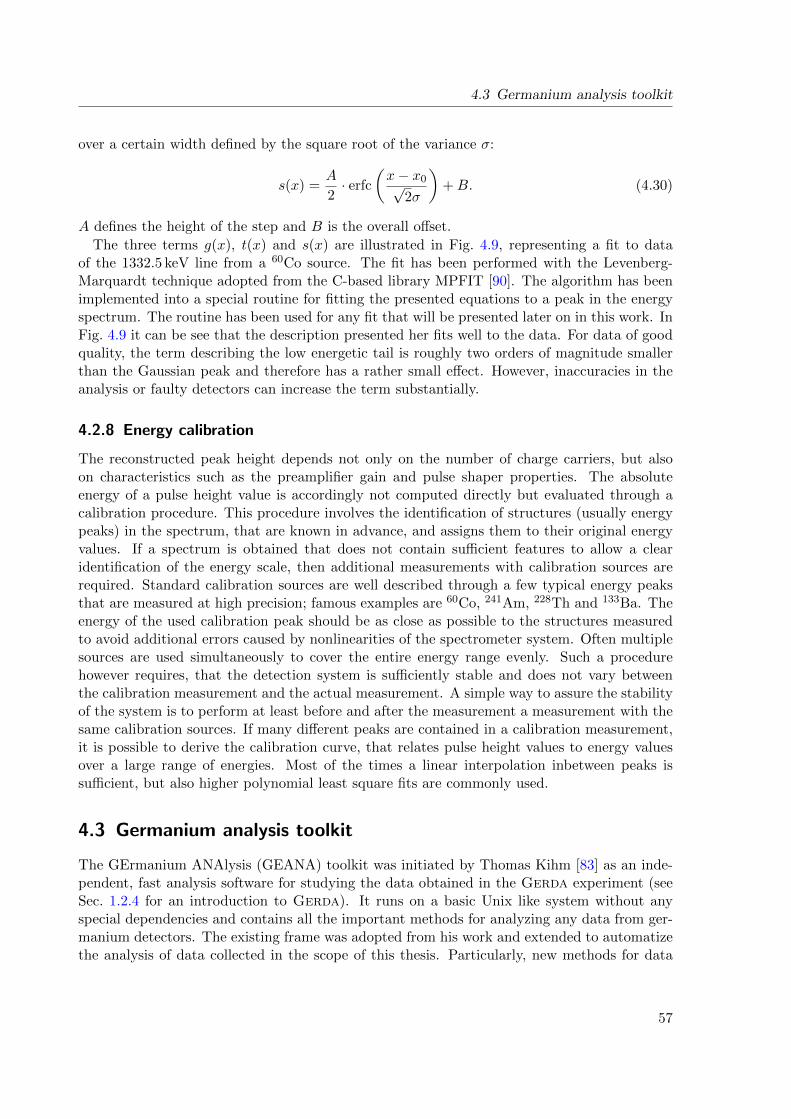
4.3 Germanium analysis toolkit
over a certain width defined by the square root of the variance σ:
s(x) =A
2· erfc
(x− x0√
2σ
)+B. (4.30)
A defines the height of the step and B is the overall offset.
The three terms g(x), t(x) and s(x) are illustrated in Fig. 4.9, representing a fit to dataof the 1332.5 keV line from a 60Co source. The fit has been performed with the Levenberg-Marquardt technique adopted from the C-based library MPFIT [90]. The algorithm has beenimplemented into a special routine for fitting the presented equations to a peak in the energyspectrum. The routine has been used for any fit that will be presented later on in this work. InFig. 4.9 it can be see that the description presented her fits well to the data. For data of goodquality, the term describing the low energetic tail is roughly two orders of magnitude smallerthan the Gaussian peak and therefore has a rather small effect. However, inaccuracies in theanalysis or faulty detectors can increase the term substantially.
4.2.8 Energy calibration
The reconstructed peak height depends not only on the number of charge carriers, but alsoon characteristics such as the preamplifier gain and pulse shaper properties. The absoluteenergy of a pulse height value is accordingly not computed directly but evaluated through acalibration procedure. This procedure involves the identification of structures (usually energypeaks) in the spectrum, that are known in advance, and assigns them to their original energyvalues. If a spectrum is obtained that does not contain sufficient features to allow a clearidentification of the energy scale, then additional measurements with calibration sources arerequired. Standard calibration sources are well described through a few typical energy peaksthat are measured at high precision; famous examples are 60Co, 241Am, 228Th and 133Ba. Theenergy of the used calibration peak should be as close as possible to the structures measuredto avoid additional errors caused by nonlinearities of the spectrometer system. Often multiplesources are used simultaneously to cover the entire energy range evenly. Such a procedurehowever requires, that the detection system is sufficiently stable and does not vary betweenthe calibration measurement and the actual measurement. A simple way to assure the stabilityof the system is to perform at least before and after the measurement a measurement with thesame calibration sources. If many different peaks are contained in a calibration measurement,it is possible to derive the calibration curve, that relates pulse height values to energy valuesover a large range of energies. Most of the times a linear interpolation inbetween peaks issufficient, but also higher polynomial least square fits are commonly used.
4.3 Germanium analysis toolkit
The GErmanium ANAlysis (GEANA) toolkit was initiated by Thomas Kihm [83] as an inde-pendent, fast analysis software for studying the data obtained in the Gerda experiment (seeSec. 1.2.4 for an introduction to Gerda). It runs on a basic Unix like system without anyspecial dependencies and contains all the important methods for analyzing any data from ger-manium detectors. The existing frame was adopted from his work and extended to automatizethe analysis of data collected in the scope of this thesis. Particularly, new methods for data
57
4 Signal acquisition, analysis and simulation
input/output and some new algorithm to use the program for data measured with a varietyof radioactive sources (e.g. peak finding methods, rise time analysis, etc.) has been added. Inthe following sections some main aspects of GEANA will be presented.
4.3.1 Program organization
GEANA consists of three main blocks, first a collection of important methods organized inlibraries, second a set of small programs that perform particular tasks of the data analysischain of germanium detectors and finally a few scripts that are used for controlling the analysischain.
The core of GEANA is an extensive set of C-style functions, that are organized in fivedifferent libraries. The libraries provide most of the functionality required for analyzing dataobtained with a germanium detector, thus aside from the standard libraries available on mostUnix systems there is no special dependency. The libraries can be individually build, arecompatible with C/C++ and are also used for a variety of other projects that require similarmethods. The methods provided by the libraries include plotting, filling of histograms, filteringof signals, reading data from and writing data to the disk, fitting peaks in histograms, findingpeaks in histograms, etc.
These libraries then are used to implement five small programs, that are specialized toperform a specific task in the sequence that ultimately leads to a reconstruction of the energyof each signal. Similar to the libraries, the individual programs are all implemented in C andcompatible with C++. The main task of these programs will be discussed in Section 4.3.4and can be summarized as indicated in Fig. 4.10 as follow: data organization, filter parameterextraction and optimization, calibration, energy reconstruction.
The sequential call of the individual programs is controlled by a few additional scripts that areimplemented in the scripting language BASH. The main script only requires a few fundamentalinformation about the data set and is from there on capable of automatically perform the entireanalysis of the provided data set. Some other scripts can be used for some more advancedplotting and fitting task and make heavy usage of GNUplot [91].
4.3.2 Data flow
A few basic configure parameters need to be given to the programs in order to be functional.These parameters can be defined in a header style setup file, that then is used to compilethe five main C-programs. Often these parameters change slightly from one type of analysisto another, in such a case it is most convenient to use a separate version of GEANA with aparticular header file. However, often analyses are similar enough, so that the same setup filecan be used. It is for example possible to run the entire data set of the Gerda experimentwith a single setup file.
The files produced during the analysis are most conveniently kept in a separate directory,that is consecutively updated as the analysis progresses. The folder contains initially onlya file defining the detector layout (if the measurement was performed with more than onedetector), but later in the analysis process other files are added. The first files that are createdfor example contain information about the organization of the files that need to be analyzed.Each program adds extensive logging files and a few important histograms to the folder, so thatthe individual steps can be checked for their validity. Each programs additionally calculates
58
4.3 Germanium analysis toolkit
a few new parameters that need to be passed to the next stage. These information flow fromone program to the next by storing them in a configuration file that is consecutively updatedby the different programs.
If requested, the final programs also produce some event based file lists. These files areorganized in an ASCII format and contain all the important values of an individual event, suchas time stamp, reconstructed energy of the incident radiation, veto flags, coincidences withother detectors etc. A small portion of the signal can also be added to the list to be furtherused to define additional background suppression parameters.
At the very end of the analysis, all important information and plots are collected on a singlehtml web page, that is stored to the same folder and allows to easily confirm that the analysisprocess was performed satisfactorily.
4.3.3 Implemented methods
In Sec. 4.2 different methods to improve the pulse height reconstruction have been discussed.All of them are implemented in GEANA and can either be directly selected or automaticallyoptimized. Before the main shaping filters are applied to the signals, the pole-zero cancellationmust be performed. Then the MSEC method that was discussed in Sec. 4.2.5 can optionally beconducted to reduce ballistic deficit effects. Only at this stage the signals are filtered with theshaping filters. There are three basic filters; the pseudo-Gaussian filter composed of 4 movingwindow average filters of the same length, the rounded-top trapezoidal filter composed of 4moving window average filters of different length, and the rounded-top cusp filter created fromtwo bidirectional low-pass filters and an additional moving window average filter. After theshaping filter the pulse height is found by a simple maximum search in a confined range aroundthe charge pulse.
These method all require that some parameters are defined in advance:
• Pole-zero: Decay time,
• MSEC: Enabled/disabled,
• pseudo-Gaussian filter: Shaping time,
• rounded-top trapezoidal filter: Shaping time, rounded-top width,
• rounded-top cusp filter: Decay of the two sided exponential, width of rounded top,
• location of the amplitude (pulse height) measurement: Time range within which a max-imum search is performed.
GEANA contains mechanisms that can be used to establish the values of all these parametersautomatically, even the optimal filter type. However, such a procedure is computational in-tensive and it is better to only search the optimal parameters from a very limited number ofpreselected values.
Once the filter parameters are established the peak height spectrum can be calculated anda calibration curve extracted. The calibration curve requires the knowledge of the energiesof the γ-rays that were used for the calibration measurement. GEANA contains some simplemethods to match these energies to the respective peaks in the spectrum in an automatedmanner.
59
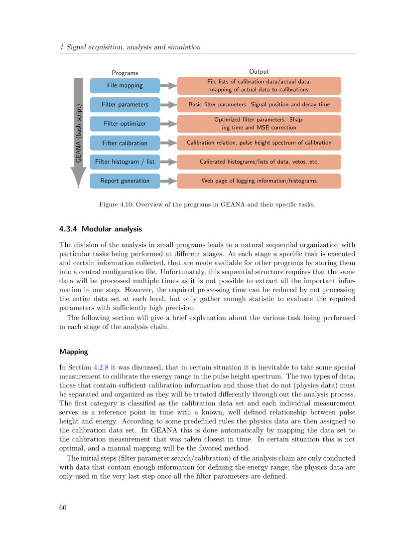
4 Signal acquisition, analysis and simulation
Programs Output
File mapping
Filter parameters
Filter optimizer
Filter calibration
Filter histogram / list
Report generation
File lists of calibration data/actual data,
mapping of actual data to calibrations
Basic filter parameters: Signal position and decay time
Optimized filter parameters: Shap-
ing time and MSE correction
Calibration relation, pulse height spectrum of calibration
Calibrated histograms/lists of data, vetos, etc.
Web page of logging information/histograms
GE
AN
A(b
ash
scri
pt)
Figure 4.10: Overview of the programs in GEANA and their specific tasks.
4.3.4 Modular analysis
The division of the analysis in small programs leads to a natural sequential organization withparticular tasks being performed at different stages. At each stage a specific task is executedand certain information collected, that are made available for other programs by storing theminto a central configuration file. Unfortunately, this sequential structure requires that the samedata will be processed multiple times as it is not possible to extract all the important infor-mation in one step. However, the required processing time can be reduced by not processingthe entire data set at each level, but only gather enough statistic to evaluate the requiredparameters with sufficiently high precision.
The following section will give a brief explanation about the various task being performedin each stage of the analysis chain.
Mapping
In Section 4.2.8 it was discussed, that in certain situation it is inevitable to take some specialmeasurement to calibrate the energy range in the pulse height spectrum. The two types of data,those that contain sufficient calibration information and those that do not (physics data) mustbe separated and organized as they will be treated differently through out the analysis process.The first category is classified as the calibration data set and each individual measurementserves as a reference point in time with a known, well defined relationship between pulseheight and energy. According to some predefined rules the physics data are then assigned tothe calibration data set. In GEANA this is done automatically by mapping the data set tothe calibration measurement that was taken closest in time. In certain situation this is notoptimal, and a manual mapping will be the favored method.
The initial steps (filter parameter search/calibration) of the analysis chain are only conductedwith data that contain enough information for defining the energy range; the physics data areonly used in the very last step once all the filter parameters are defined.
60
4.3 Germanium analysis toolkit
Filter parameters
The filters described in Sec. 4.2.2 only work if some fundamental input parameters are given.The most crucial parameter is the decay time of the preamplifier required to perform the pole-zero cancellation, which will be evaluated by the second stage of GEANA. One way to find theexact value of the decay time is to sum up a specific amount of input signals and to calculatethe average signal shape. This signal will have a decaying tail with a decay constant close tothe decay time of the preamplifier. However, this value can be distorted by preceding events(pile-ups). To correct this, the decay constant in the region before the pulse is additionallycalculated and subtracted from the value found in the tail.
The average signal provides some additional information. The position of the rising edge ofthe pulse can be found to reduce the range of the following filters to a small region around thisedge and define the range in which the maximum search is performed.
Filter optimization
The next stage is to find the optimal set of filters: The ballistic deficit may or may not becorrected (MSEC on/off), and the filter type and shaping time must be defined.
Thus, a method was implemented that optimizes the filter type, shaping time and MSECby filtering a part of the calibration data set for all possible combinations of a user providedparameter list. The energy resolution of a specific energy peak is determined and the parameterset with the best energy resolution is selected. As the number of filter combinations increasesquickly with an increasing number of parameters, it is beneficial to reduce the set of parameters,that need to be checked, to a minimum.
Filter calibration
The optimal set of parameters is used in the next stage to filter the calibration data set. In themapping process calibration data sets were organized into blocks, and each calibration data setis individually filtered to take into account changes between consecutive measurements. Theerrors that are introduced by the nonlinear response of the data acquisition systems can bereduced by having numerous calibration peaks available. The energy range between peaks islinearly interpolated.
The matching between observed peaks in the pulse height spectrum and the γ-ray lines canbe automated. A simple approach used in GEANA is to calculate ratios between the energypeaks and then compare them to ratios between γ-ray lines to look for the best match.
If shifts between two calibration measurements are too large both calibrations are rejectedand the data sets taken between the two calibration measurement excluded from the analysis.
Data filtering
In the last stage, the filtering of the physics data is performed. In this process, a calibratedenergy spectrum (histogram) is produced by applying the previously defined calibration rela-tions. In addition, in that process also the event lists, that contain all the information on anevent-by-event basis, are created. Often, it is also required to have calibrated histograms andevent list of the calibration data sets, these data sets are thus processed again to create allrequired output files.
61
4 Signal acquisition, analysis and simulation
After finalizing the analysis, all relevant information will be collected from the differentoutput files and the html web page will be created with all relevant information about a givenanalysis.
4.4 Pulse shape simulation
The underlying physics of signal formation can be studied by performing simulations. Forthis purpose an existing library (simulation toolkit), the Agata Detector simulation Library(ADL3) was adopted [92]. The Advanced GAmma Tracking Array (Agata) is a European largescale γ-ray spectrometer project that tries to make use of segmented high-purity germaniumcrystals to accurately determine the energy, time and position of every interaction of γ-rays[93]. The reconstruction of the interaction position from the pulses acquired at the differentsegments requires very precise simulations of pulses at different interaction positions, thus theneed for such a simulation library emerged.
In ADL3, the structure and calculation of the different potentials and fields is partiallybased on a commercial software [94]. The simulation of the pulses from these fields then wasnewly implemented and is based on algorithm and physical models studied by the Agatacollaboration [95, 96].
The initial library was extended for the work presented in this thesis with field calculationsthat take variable permittivity in the medium into account and with geometrical models fordetector types that were used for the Gerda experiment (see Sec. 1.2.4 for more informationabout Gerda). The field calculation is similar to an algorithm developed by part of theMajorana collaboration in Oak Ridge, Tennessee [97], and was tested carefully. The extendedADL3 library is currently used by other groups within the Gerda collaboration and a groupof Agata at the University of Liverpool [98].
ADL3 is implemented in C, compatible with C++ and only depends on the standard Clibraries available on most Unix like systems. The main functionality is collected in libraries,that then can be used to write dedicated programs.
The library is divided in two parts, one dedicated for calculating the electric and weightingpotential, the other for calculating the signal shape for given potentials and a specific interactionlocation. This division is usually also kept in the usage of the library, as the calculation of thepotentials takes some time, but they can be conveniently stored to a file and then be reusedby many different programs for the simulation of the detailed pulse shape. Furthermore, theevaluation of the potential is already sufficient to study some characteristics of the detectors,such as the depletion voltage.
4.4.1 Field simulation
The first step in simulating the pulse shape of an event is to calculate the electric potential andthe weighting potential for a given detector geometry. The next sections describe a method toachieve this for any predefined detector geometry.
62
4.4 Pulse shape simulation
Electric potential and field
The electric potential is derived from the Macroscopic Gaussian Law, one of the four Maxwellequations:
~∇ · ~D = ρf , where ~D = ε ~E and ~∇φ = − ~E. (4.31)
In these equations ρf is the free charge and φ the electric potential. The displacement field ~D
is related to the electric field ~E by the permittivity ε, which in the most general case can be amatrix and a function of the position. In the field simulations presented here, the permittivitywas considered to be a scalar, however it was not considered as constant throughout thesimulation volume so that a combination of different materials can be simulated. From equation4.31 the following equation can be derived (the position dependence of all variables is for clarityindicated explicitly):
∇2φ(~x) · ε(~x) +∇φ(~x) · ∇ε(~x) = ρf (~x). (4.32)
In most situations, this equation is sufficient to evaluate the potentials in a germanium detector.It incorporates the space charges within the detector bulk, that is created by electrons andholes moving along the electric field into the highly doped medium. Moreover, it also takesinto account variabilities in the permittivity and thus correctly calculates the potentials inregions that are not built from germanium. If such regions are neglected the permittivity canbe assumed as constant and the equation reduced to the Poisson equation:
∇2φ(~x) = ρf (~x)/ε, (4.33)
where the permittivity usually is simplified to be ε = ε0 · εr with εr = 16 in germanium andε0 being the vacuum permittivity. In certain cases the space charge is zero and the Laplaceequation can be used:
∇2φ(~x) = 0. (4.34)
Equations 4.32, 4.33 and 4.34 are all implemented into ADL3 in order to be capable of per-form the simulations presented in later chapters. To solve the respective differential equation amethod called ‘successive over relaxation’ [99] is used. For this purpose the detector structureis represented on a grid, with each grid point having specific attributes (a value for the permit-tivity, space charge and electric potential). In multiple steps, by iterating over the completegrid, the physical solution of the differential equation is approached until a certain predefinedprecision is reached and the algorithm is stopped. In each step, a new value is calculated atevery point of the grid, by averaging the nearest neighbors and weighting this value with thelast value at this position. This approach converges fast.
From the electric potential the electric field can be derived by solving the third equation in4.31.
Weighting potential
The Shockley-Ramo theorem was discussed in Sec. 2.2.6 and the weighting potential definedthat facilitates the calculation of the induced charge into an electrode. Here, a simple recipefor the calculation of the weighting potential is provided to summarize the most importantfindings:
• The selected electrode is at unit potential (=1).
63
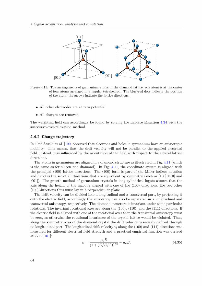
4 Signal acquisition, analysis and simulation
[100]
[001][010]
Figure 4.11: The arrangements of germanium atoms in the diamond lattice: one atom is at the centerof four atoms arranged in a regular tetrahedron. The blue/red dots indicate the positionof the atom, the arrows indicate the lattice directions.
• All other electrodes are at zero potential.
• All charges are removed.
The weighting field can accordingly be found by solving the Laplace Equation 4.34 with thesuccessive-over-relaxation method.
4.4.2 Charge trajectory
In 1956 Sasaki et al. [100] observed that electrons and holes in germanium have an anisotropicmobility. This means, that the drift velocity will not be parallel to the applied electricalfield, instead, it is influenced by the orientation of the field with respect to the crystal latticedirections.
The atoms in germanium are aligned in a diamond structure as illustrated in Fig. 4.11 (whichis the same as for silicon and diamond). In Fig. 4.11, the coordinate system is aligned withthe principal 〈100〉 lattice directions. The 〈100〉 form is part of the Miller indices notationand denotes the set of all directions that are equivalent by symmetry (such as [100],[010] and[001]). The growth method of germanium crystals in long cylindrical ingots assures that theaxis along the height of the ingot is aligned with one of the 〈100〉 directions, the two other〈100〉 directions thus must lay in a perpendicular plane.
The drift velocity can be divided into a longitudinal and a transversal part, by projecting itonto the electric field, accordingly the anisotropy can also be separated in a longitudinal andtransversal anisotropy, respectively. The diamond structure is invariant under some particularrotations. The invariant rotational axes are along the 〈100〉, 〈110〉, and the 〈111〉 directions. Ifthe electric field is aligned with one of the rotational axes then the transversal anisotropy mustbe zero, as otherwise the rotational invariance of the crystal lattice would be violated. Thus,along the symmetry axes of the diamond crystal the drift velocity is entirely defined throughits longitudinal part. The longitudinal drift velocity vl along the 〈100〉 and 〈111〉 directions wasmeasured for different electrical field strength and a practical empirical function was derivedat 77 K [101]:
vl =µ0E
(1 + (E/E0)β)1/β− µnE. (4.35)
64
4.4 Pulse shape simulation
At low fields (E E0) the equation reduces to the normal proportional dependence vl = µ0E,at intermediate electric field strength the deviation from this dependence is modeled throughthe fit parameters β and E0. A negative differential mobility [102] has been observe at highelectric field (above 3 kV/cm) therefore the term µnE has been added to account for this effect.
In order to calculate the drift velocity for any orientation of the electric field to the crystallattice, the details of the band structure in germanium must be studied. Only the bandstructure in close vicinity of the energy gap is of importance as phonon losses prohibit thepopulation of high energetic levels. The parameters defining the shape of the energy bandnear the band gap for a given orientation of the electric field to the crystal lattice are theeffective masses, which are known from other experimental studies [101]. Both, for electronsand holes, there exist some simplified empirical formula, that adds two more fit parameters todefine these dependencies and fix the drift velocity for any orientation of the electric field andthe crystal lattice [95, 96, 101]. In typical germanium detectors, the additional term for thenegative differential mobility can be neglected as the field strength is below 3 kV/cm. For eachcharge carrier type there are 6 remaining empirical parameters, β and E0 to define the driftvelocities for a given field strength along the 〈100〉 and 〈111〉 directions respectively and twomore parameters to perform a transformation to any orientation of the field and the crystallattice. This model agrees with experimental data in that not only the magnitude of the driftvelocity varies, but also a non zero transversal component appears, that points towards theaxes with the highest longitudinal drift velocity.
The details of the models that define the drift velocities are implemented in ADL3 and thenecessary empirical fit parameters can be either evaluated by a global fit to measurements orby assuming the detector material to be close to the one used in the publications describingthe respective models.
65
5 Point contact optimization
A large variety of different PCGe detectors is being used in fundamental research. Some of thechoices for a particular detector shape and point contact size can be found in consideration inregards to the research that should be conducted with the detector. However, also limitationsin the fabrication process do affect the PCGe detector geometry.
The impact of differences in the shape and size of the point contact has not yet been experi-mentally investigated in detail. The largest study of variations in detectors so far was conductedby the Gerda collaboration during a characterization campaign of the 30 new BEGe detectors[63]. Furthermore, also the Majorana collaboration has recently released first results on thecharacterization of their detectors [103]. The collected data show that crystal variation aredominant and that there is practically no correlation between specific geometrical features.The reason for this is rather simple – the detectors have different impurity concentrations andnot all the material could have been processed simultaneously, thus the crystal quality varies.Furthermore, it is often hard to entangle intrinsic properties of the crystal from effects causedby the design.
In order to circumvent the material and diode variability, the study presented in this disserta-tion tries to go into a new direction. Instead of measuring a large amount of different detectors,data from only two detectors are gathered, that are consecutively modified by varying onlythe least amount of parameters necessary (as discussed later on the groove and point contactsize). This approach allows to study the detectors response to the geometrical modificationunder constant conditions in terms of intrinsic material properties. The study is performedwith two almost identical detectors simultaneously to rule out systematic effects and confirmthe observations with a second set of measurements.
The detectors that are study have been produced by Canberra N.V. in Olen, Belgium andfollow the typical shape of their Broad Energy Germanium (BEGe) detectors, with a groovebetween the two electrodes. The discussion here will be limited to this type of detectors.
The first part of this chapter will describe how the design of the detectors has been definedwith simulations in ADL3. In the second part the geometry of the two actually produceddetectors will be described.
5.1 Simulation-based investigation of geometrical modification
In this section it is assumed that a detector of a given volume should be fabricated. Thestarting point is a Gerda-like detector with 3.5 cm height and 3.5 cm radius, thus a volumeof 134.7 cm2 and a weight of 717 g. This design then is consecutively altered to study howthe performance can be optimized for particular applications. It must be kept in mind thatthis discussion is primarily aimed at applications in fundamental research. In this field thedetectors require are large volumes with a low surface-to-volume ratio, low energy thresholdand little noise.
The electric field simulated with ADL3 are used to study the effects of geometrical mod-
66

5.1 Simulation-based investigation of geometrical modification
0.5
1.0
1.5
2.0
2.5
3.0
3.5
4.0
0.2 0.4 0.6 0.8 1 1.2 1.4 1.6 1.8 21.05
1.10
1.15
1.20
1.25
1.30
1.35
1.40
Dep
leti
onvo
ltag
e[k
V]
Su
rface-to-volum
eratio
[1/cm]
Aspect ratio
8.0 mm point contact radius4.0 mm point contact radius
Figure 5.1: The depletion voltage of two different detector configuration are shown as a function of theaspect ratio (radius/height) for a detector of 717 g. In addition also the surface-to-volumeratio is indicated. The impurity concentration was chosen to be constant throughout thedetector and at 1010 /cm3. Simulated with ADL3.
ifications on detector properties. To distinguish a good geometry from a not so good one,it is necessary to define a quality factor (figure of merit). This is not straight forward. Animportant factor in a detector is a homogeneous electric field distribution to assure completecharge collection throughout the detector volume. PCGe detectors are relatively suboptimalin that concern, the fields in coaxial detectors are usually more homogeneous. However, PCGedetectors have other beneficial features (see Sec. 3) that must be conserved. Thus homogeneousfields are important as long as they do conserve the other features, such as low capacitanceand good pulse shape properties. The homogeneity of the field can be controlled by the oper-ational voltage of the detector, which must be well above depletion. However, the operationalvoltage should not exceed ∼ 5 keV as effects from leakage currents more likely affect the diodesperformance at high voltages. As a good homogeneity of the field for a given voltage usuallycoincides with a low depletion voltage, the depletion voltage is chosen to be the figure of meritfor the detector geometry and can easily be simulated in ADL3 and compared for differentgeometries.
5.1.1 Aspect ratio
The importance of a homogeneous electric field must be weighted against a certain surface-to-volume ratio, as the geometry with the most homogeneous field most likely is not the onewith the best surface-to-volume ratio. Fig. 5.1, shows the depletion voltage as a function ofthe aspect ratio of a detector (the ratio between the radius and the height) for two differentpoint contact radius (8 mm and 4 mm). It can be observed that at the best surface-to-volumeratio the depletion voltage is highest, thus the field configuration not at the optimum. At anaspect ratio of 1-1.2 there is a small dent in the depletion voltage and for higher aspect ratiothe depletion voltage decreases slowly. It seems reasonable to choose the aspect ratio such,that it is placed at the value of the dent in the depletion voltage. Below the dent the depletion
67
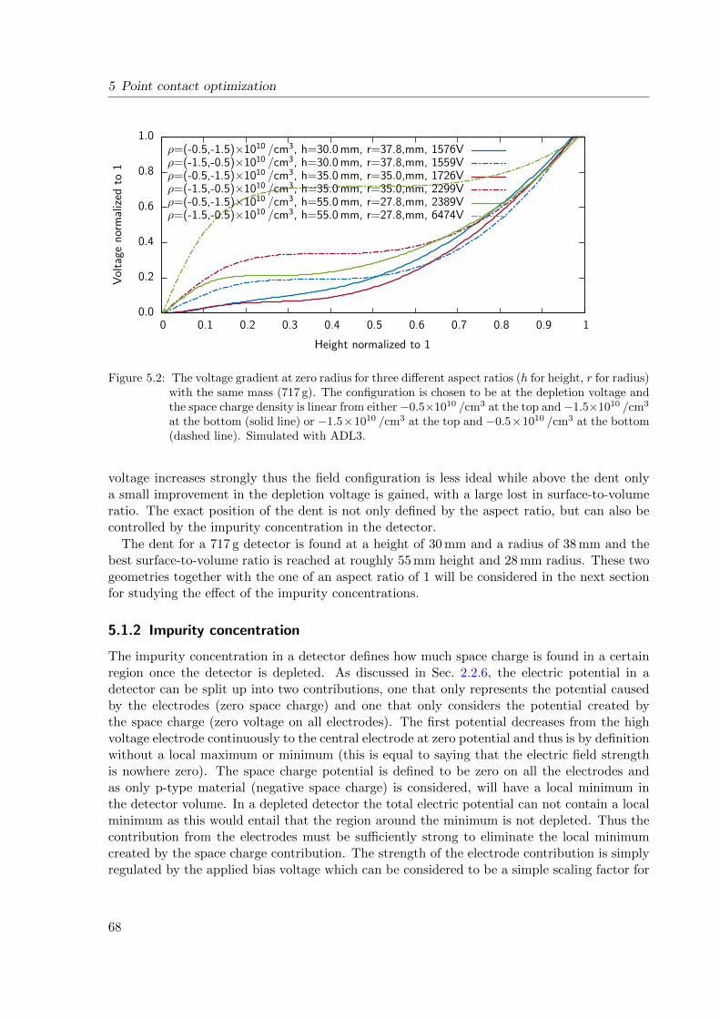
5 Point contact optimization
0.0
0.2
0.4
0.6
0.8
1.0
0 0.1 0.2 0.3 0.4 0.5 0.6 0.7 0.8 0.9 1
Vol
tage
nor
mal
ized
to1
Height normalized to 1
ρ=(-0.5,-1.5)×1010 /cm3, h=30.0 mm, r=37.8,mm, 1576Vρ=(-1.5,-0.5)×1010 /cm3, h=30.0 mm, r=37.8,mm, 1559Vρ=(-0.5,-1.5)×1010 /cm3, h=35.0 mm, r=35.0,mm, 1726Vρ=(-1.5,-0.5)×1010 /cm3, h=35.0 mm, r=35.0,mm, 2299Vρ=(-0.5,-1.5)×1010 /cm3, h=55.0 mm, r=27.8,mm, 2389Vρ=(-1.5,-0.5)×1010 /cm3, h=55.0 mm, r=27.8,mm, 6474V
Figure 5.2: The voltage gradient at zero radius for three different aspect ratios (h for height, r for radius)with the same mass (717 g). The configuration is chosen to be at the depletion voltage andthe space charge density is linear from either−0.5×10¹⁰ /cm3 at the top and−1.5×10¹⁰ /cm3
at the bottom (solid line) or −1.5×10¹⁰ /cm3 at the top and −0.5×10¹⁰ /cm3 at the bottom(dashed line). Simulated with ADL3.
voltage increases strongly thus the field configuration is less ideal while above the dent onlya small improvement in the depletion voltage is gained, with a large lost in surface-to-volumeratio. The exact position of the dent is not only defined by the aspect ratio, but can also becontrolled by the impurity concentration in the detector.
The dent for a 717 g detector is found at a height of 30 mm and a radius of 38 mm and thebest surface-to-volume ratio is reached at roughly 55 mm height and 28 mm radius. These twogeometries together with the one of an aspect ratio of 1 will be considered in the next sectionfor studying the effect of the impurity concentrations.
5.1.2 Impurity concentration
The impurity concentration in a detector defines how much space charge is found in a certainregion once the detector is depleted. As discussed in Sec. 2.2.6, the electric potential in adetector can be split up into two contributions, one that only represents the potential causedby the electrodes (zero space charge) and one that only considers the potential created bythe space charge (zero voltage on all electrodes). The first potential decreases from the highvoltage electrode continuously to the central electrode at zero potential and thus is by definitionwithout a local maximum or minimum (this is equal to saying that the electric field strengthis nowhere zero). The space charge potential is defined to be zero on all the electrodes andas only p-type material (negative space charge) is considered, will have a local minimum inthe detector volume. In a depleted detector the total electric potential can not contain a localminimum as this would entail that the region around the minimum is not depleted. Thus thecontribution from the electrodes must be sufficiently strong to eliminate the local minimumcreated by the space charge contribution. The strength of the electrode contribution is simplyregulated by the applied bias voltage which can be considered to be a simple scaling factor for
68
5.1 Simulation-based investigation of geometrical modification
the electric potential created by the electrodes at unit voltage. The voltage that needs to beapplied to exactly remove the local minimum is the depletion voltage.
This discussion reveals the actual impact of space charge onto the electric field configurationin a diode: If the space charge is zero, which requires that there are no impurities (intrinsicmaterial), then the diode is depleted at any bias voltage. At non zero space charge, the electricpotential is modified by the space charge in that the gradient in some regions is increased,while in others reduced. In the production of PCGe detectors, low impurity concentrations areusually favored as this leads to less trapping, however impurity gradients are very practical tocreate a more uniform field and remove regions with low drift velocities.
The effect is represented in Fig. 5.2 that assumes an impurity concentration gradient alongthe height of the detector. It can be seen that for either aspect ratio the field (derivativeof the potential) is more homogeneous if the space charge is chosen to be more negative onthe bottom (the side with the point contact) than on the top. In all configurations but theshort cylinder one (30 mm height, 38 mm radius) the depletion voltage is also lower for thatconfiguration. The figure also highlights that the field configuration is worst (long stretches oflow field strength) if the aspect ratio is chosen to be ideal in regards to the surface-to-volumeratio and is better the shorter the cylinder is chosen to be. However, choosing a very shortcylinder will cause low field regions along the radial direction, which is also suboptimal.
The long straight stretches of some of the curves in Fig. 5.2 furthermore explain an obser-vation made later in the experimental evaluation of the detectors – an undepleted bubble inthe center of the detector. The curves in Fig. 5.2 are drawn just at the depletion voltage. Theelectric field falls off continuously from the high voltage electrode to the depletion border inthe n-type material. If the applied voltage is slightly reduced the curves with long straightstretches would obtain a local minimum in the center of the detector. Such a local minimum isnot physical, instead of reaching a local minimum the electric potential in that region takes aconstant value. A constant potential (zero electric field) means that this region is not depleted.Instead, a local undepleted bubble is formed.
5.1.3 Point contact size and groove width
In Sec. 3.3 it has been discussed that the strength of a PCGe detector is the small capacitancerelated to the small size of the point contact. Accordingly, it is desirable to reduce the size ofthe point contact, but this should not be on the expense of a homogeneous field distributionin the detector.
Fig. 5.3 shows the relation between the point contact radius, the width of the groove (mea-sured from the point contact to the high voltage contact) and the depletion voltage for thethree geometries described in the previous sections. The left plots show that there is a smallband along a particular set of parameters where the depletion voltage is minimal. Therefore,the width of the groove can be carefully selected as a function of the point contact radiusto stay within the band of minimal depletion voltage. In the right plot it can be seen, thatif one chooses the groove width accordingly then indeed the increase in depletion voltage issmall. A maximal increase of 200 V when going from a radius of 10 mm to a radius of 0.1 mmis measured. The change is less drastic in the case of a long cylindrical shape, that shows astable curve at a relatively high voltage compared to the other two geometries. The figure alsoshows, that there is an almost linear relation between the point contact radius and the optimalgroove width. A large point contact radius asks for a small groove width, a small point contact
69
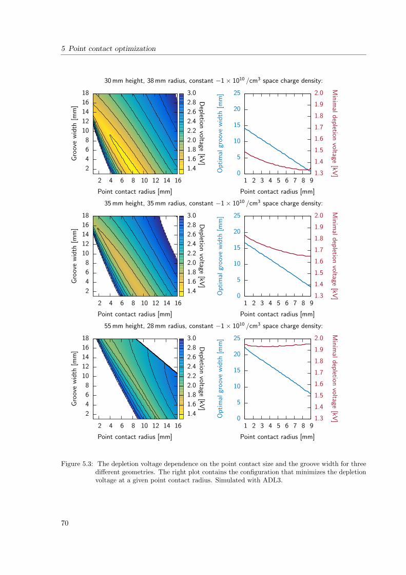
5 Point contact optimization
30 mm height, 38 mm radius, constant −1× 10¹⁰ /cm3 space charge density:
Point contact radius [mm]
Gro
ove
wid
th[m
m]
2
4
6
8
10
12
14
16
18
2 4 6 8 10 12 14 16
1.4
1.6
1.8
2.0
2.2
2.4
2.6
2.8
3.0
Dep
letionvoltage
[kV]
0
5
10
15
20
25
1 2 3 4 5 6 7 8 91.3
1.4
1.5
1.6
1.7
1.8
1.9
2.0
Op
tim
algr
oov
ew
idth
[mm
]
Min
imal
dep
letionvoltage
[kV]
Point contact radius [mm]
35 mm height, 35 mm radius, constant −1× 10¹⁰ /cm3 space charge density:
Point contact radius [mm]
Gro
ove
wid
th[m
m]
2
4
6
8
10
12
14
16
18
2 4 6 8 10 12 14 16
1.4
1.6
1.8
2.0
2.2
2.4
2.6
2.8
3.0
Dep
letionvoltage
[kV]
0
5
10
15
20
25
1 2 3 4 5 6 7 8 91.3
1.4
1.5
1.6
1.7
1.8
1.9
2.0O
pti
mal
gro
ove
wid
th[m
m]
Min
imal
dep
letionvoltage
[kV]
Point contact radius [mm]
55 mm height, 28 mm radius, constant −1× 10¹⁰ /cm3 space charge density:
Point contact radius [mm]
Gro
ove
wid
th[m
m]
2
4
6
8
10
12
14
16
18
2 4 6 8 10 12 14 16
1.4
1.6
1.8
2.0
2.2
2.4
2.6
2.8
3.0
Dep
letionvoltage
[kV]
0
5
10
15
20
25
1 2 3 4 5 6 7 8 91.3
1.4
1.5
1.6
1.7
1.8
1.9
2.0
Op
tim
algr
oov
ew
idth
[mm
]
Min
imal
dep
letionvoltage
[kV]
Point contact radius [mm]
Figure 5.3: The depletion voltage dependence on the point contact size and the groove width for threedifferent geometries. The right plot contains the configuration that minimizes the depletionvoltage at a given point contact radius. Simulated with ADL3.
70
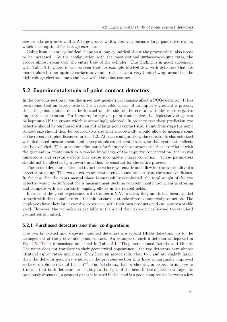
5.2 Experimental study of point contact detectors
size for a large groove width. A large groove width, however, means a large passivated region,which is suboptimal for leakage currents.
Going from a short cylindrical shape to a long cylindrical shape the groove width also needsto be increased. At the configuration with the most optimal surface-to-volume ratio, thegroove almost spans over the entire base of the cylinder. This finding is in good agreementwith Table 3.1, where it can be seen that for example Majorana, with detectors that aremore tailored to an optimal surface-to-volume ratio, have a very limited wrap around of thehigh voltage electrode onto the base with the point contact.
5.2 Experimental study of point contact detectors
In the previous section it was discussed how geometrical changes affect a PCGe detector. It hasbeen found that an aspect-ratio of 1 is a reasonable choice. If an impurity gradient is present,then the point contact must be located on the side of the crystal with the more negativeimpurity concentration. Furthermore, for a given point contact size, the depletion voltage canbe kept small if the groove width is accordingly adopted. In order to test these prediction twodetector should be purchased with an initial large point contact size. In multiple steps the pointcontact size should then be reduced to a size that theoretically should allow to measure someof the research topics discussed in Sec. 1.2. At each configuration, the detector is characterizedwith dedicated measurements and a very stable experimental setup, so that systematic effectscan be excluded. This procedure eliminates furthermore most systematic that are related withthe germanium crystal such as a precise knowledge of the impurity concentration, the crystaldimensions and crystal defects that cause incomplete charge collection. These parametersshould not be affected by a rework and thus be constant for the entire process.
The second detector is intended to further reduce systematic and allow for the eventuality of adetector breaking. The two detectors are characterized simultaneously at the same conditions.In the case that the experimental phase is successfully terminated, the total weight of the twodetector would be sufficient for a measurement such as coherent neutrino-nucleus scatteringand compete with the currently ongoing efforts in the related fields.
Because of the good experiences with Canberra N.V. in Olen, Belgium, it has been decidedto work with this manufacturer. Its main business is standardized commercial production. Theemployees have therefore extensive experience with their own products and can assure a stableyield. However, the technologies available to them and their experiences beyond the standardgeometries is limited.
5.2.1 Purchased detectors and their configurations
The two fabricated and stepwise modified detectors are typical BEGe detectors, up to thearrangement of the groove and point contact. An example of such a detector is depicted inFig. 2.5. Their dimensions are listed in Table 5.1. They were named Asterix and Obelix.The name does not translate to their geometrical appearance – the two detectors have almostidentical aspect ratios and mass. They have an aspect ratio close to 1 and are slightly largerthan the detector geometry studied in the previous section thus have a marginally improvedsurface-to-volume ratio of 1.11 cm−1. Fig. 5.4 shows, that by choosing an aspect ratio close to1 means that both detectors are slightly to the right of the bend in the depletion voltage. Aspreviously discussed, a geometry that is located in the bend is a good compromise between a low
71
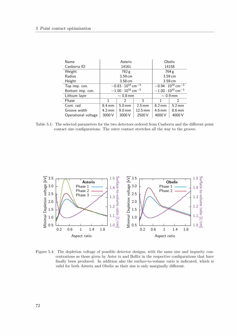
5 Point contact optimization
Name Asterix ObelixCanberra ID 14161 14158Weight 762 g 764 gRadius 3.59 cm 3.59 cmHeight 3.58 cm 3.59 cmTop imp. con. −0.83 · 1010 cm−3 −0.94 · 1010 cm−3
Bottom imp. con. −1.00 · 1010 cm−3 −1.00 · 1010 cm−3
Lithium layer ∼ 0.8 mm ∼ 0.9 mmPhase 1 2 3 1 2Cont. rad. 8.4 mm 5.0 mm 2.5 mm 8.2 mm 5.2 mmGroove width 4.2 mm 9.0 mm 12.5 mm 4.6 mm 8.6 mmOperational voltage 3000 V 3000 V 2500 V 4000 V 4000 V
Table 5.1: The selected parameters for the two detectors ordered from Canberra and the different pointcontact size configurations. The outer contact stretches all the way to the groove.
0.5
1.0
1.5
2.0
2.5
3.0
3.5
0.2 0.6 1 1.4 1.81.0
1.1
1.2
1.3
1.4
1.5
Min
imal
Dep
leti
onvo
ltag
e[k
V] S
urface-to-volu
me
ratio[1/cm
]
Aspect ratio
AsterixPhase 1Phase 2Phase 3
0.5
1.0
1.5
2.0
2.5
3.0
3.5
0.2 0.6 1 1.4 1.81.0
1.1
1.2
1.3
1.4
1.5
Min
imal
Dep
leti
onvo
ltag
e[k
V] S
urface-to-volu
me
ratio[1/cm
]
Aspect ratio
ObelixPhase 1Phase 2
Figure 5.4: The depletion voltage of possible detector designs, with the same size and impurity con-centrations as those given by Aster ix and Bollix in the respective configurations that havefinally been produced. In addition also the surface-to-volume ratio is indicated, which isvalid for both Asterix and Obelix as their size is only marginally different.
72
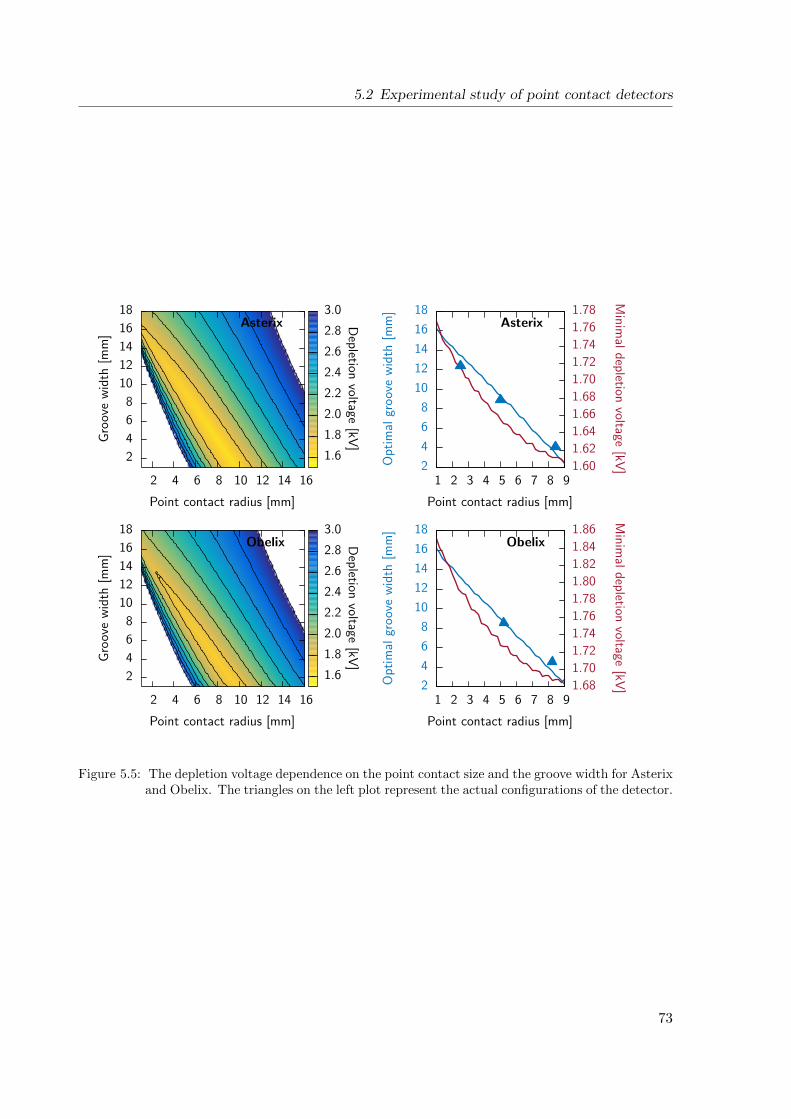
5.2 Experimental study of point contact detectors
Point contact radius [mm]
Gro
ove
wid
th[m
m]
Asterix
2
4
6
8
10
12
14
16
18
2 4 6 8 10 12 14 16
1.6
1.8
2.0
2.2
2.4
2.6
2.8
3.0
Dep
letionvoltage
[kV]
2
4
6
8
10
12
14
16
18
1 2 3 4 5 6 7 8 91.60
1.62
1.64
1.66
1.68
1.70
1.72
1.74
1.76
1.78
Op
tim
algr
oov
ew
idth
[mm
]
Min
imal
dep
letionvoltage
[kV]
Point contact radius [mm]
Asterix
Point contact radius [mm]
Gro
ove
wid
th[m
m]
Obelix
2
4
6
8
10
12
14
16
18
2 4 6 8 10 12 14 16
1.6
1.8
2.0
2.2
2.4
2.6
2.8
3.0
Dep
letionvoltage
[kV]
2
4
6
8
10
12
14
16
18
1 2 3 4 5 6 7 8 91.68
1.70
1.72
1.74
1.76
1.78
1.80
1.82
1.84
1.86
Op
tim
algr
oov
ew
idth
[mm
]
Min
imal
dep
letionvoltage
[kV]
Point contact radius [mm]
Obelix
Figure 5.5: The depletion voltage dependence on the point contact size and the groove width for Asterixand Obelix. The triangles on the left plot represent the actual configurations of the detector.
73
5 Point contact optimization
depletion voltage and a good surface-to-volume ratio. The reason why the bend appears ratherat an aspect ratio of 1 instead of 1.2 (see Sec. 5.1.1) is the different impurity concentrationprofile. The impurity concentrations in both detectors are close, however, Asterix has a slightlyhigher gradient. The impurity concentration was chosen to be more negative on the side withthe point contact (bottom side). This choice reflects the finding from Sec. 5.1.2 and is commonpractice at Canberra.
The point contact sizes were chosen to start at a relatively large value and should reach inthe final configuration a diameter of roughly 5 mm. The groove width was determined withthe simulations according to a chosen point contact radius; the exact dependencies are shownin Fig. 5.5. The actual contact radius and groove width have been defined by the availabledriller sizes at Canberra and deviate slightly from the optimum (see left panels of Fig. 5.5).
74
6 Experimental setup and measurement protocol
In this chapter a brief overview of the experimental setup, that was especially put togetherfor the characterization measurements of the two detectors is provided. Furthermore, also themost important measurements will be discussed.
6.1 Experimental setup
The measurements are performed on ground level. This means that the overburden is verysmall and most of the cosmic radiation still can reach the detector. However, the measurementsused in the characterization all involve relatively strong radioactive sources, which induce asignal much stronger than the cosmic background. Thus, this location, although not optimalis sufficient.
The room is equipped with an electronics rack, a computer and two measurement tables anda picture of it is shown in Fig. 6.1.
6.1.1 Cryostat and dewar
The two detector are mounted in two separate 7500SL Canberra cryostat (see Fig. 6.2). Thecryostat housing (end-cap) is made of 1.5 mm thick aluminum, that allows γ-rays above afew tenth of keV to penetrate into the cryostat and hit the detector. The housing containsa vacuum chamber with the detector and some parts of the preamplifier placed in vacuum.The vacuum chamber is connected to a long dipstick, that is insert into the neck of a 30 literdewar filled with liquid nitrogen. The dipstick transfers heat from the detector to the liquidnitrogen and assures that the detector is kept at a constant operational temperature. Theboiling temperature of liquid nitrogen is 77 K however the detector is usually kept at a slightlyhigher temperature.
The cryostat is equipped with a 2002CSL charge sensitive preamplifier. Parts of the pream-plifier, in particular the field-effect transistor (FET), is kept at low temperature to reducenoise, while the remaining preamplifier is at room temperature. The preamplifier is equippedwith a 5 GΩ feedback resistor and a 0.5 pF feedback capacitor. After the first amplificationthe signal is pole-zero corrected, differentiated and integrated to finally obtain a decay timeof roughly 50µs. The pulser resolution is according to Canberra 360 eV. A simplified diagramof the preamplifier setup is given in Fig. 6.3. The preamplifier has two outputs, one named’energy’ and one named ’timing’. The signal at the two outputs only differ marginally, forthe characterization measurement only the energy output was used. The preamplifier has twoinputs, one for the high voltage and one for a test pulser. A test point furthermore allows tomeasure the leakage current of the detector.
The detectors have been installed after each reprocessing step into the same cryostat toassure that there are no changes in the preamplifier setup. During the characterization mea-surement of the first configuration (Phase 1) the FET of Asterix broke and needed to bereplaced. All measurements have been repeated after the replacement of the FET. The setup
75
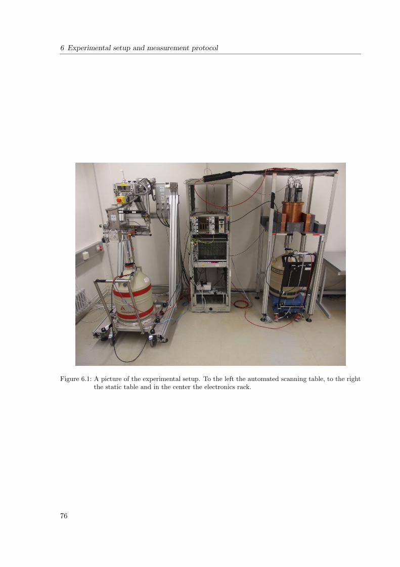
6 Experimental setup and measurement protocol
Figure 6.1: A picture of the experimental setup. To the left the automated scanning table, to the rightthe static table and in the center the electronics rack.
76
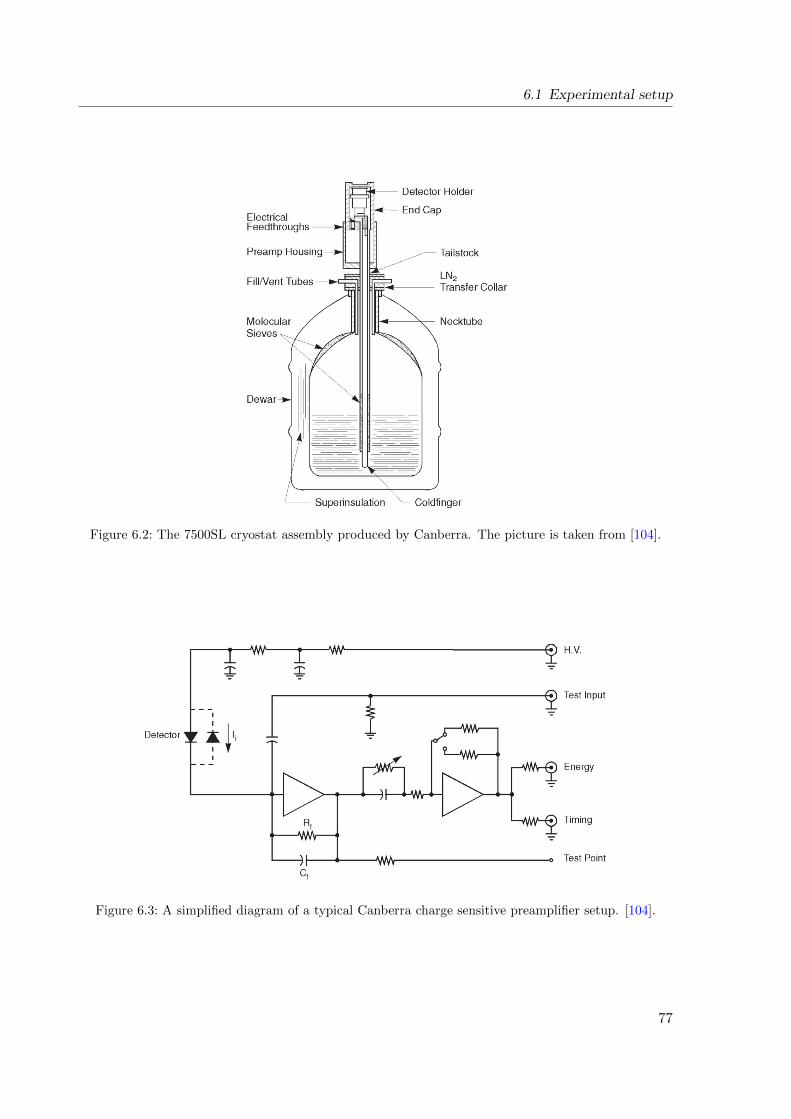
6.1 Experimental setup
Figure 6.2: The 7500SL cryostat assembly produced by Canberra. The picture is taken from [104].
Figure 6.3: A simplified diagram of a typical Canberra charge sensitive preamplifier setup. [104].
77
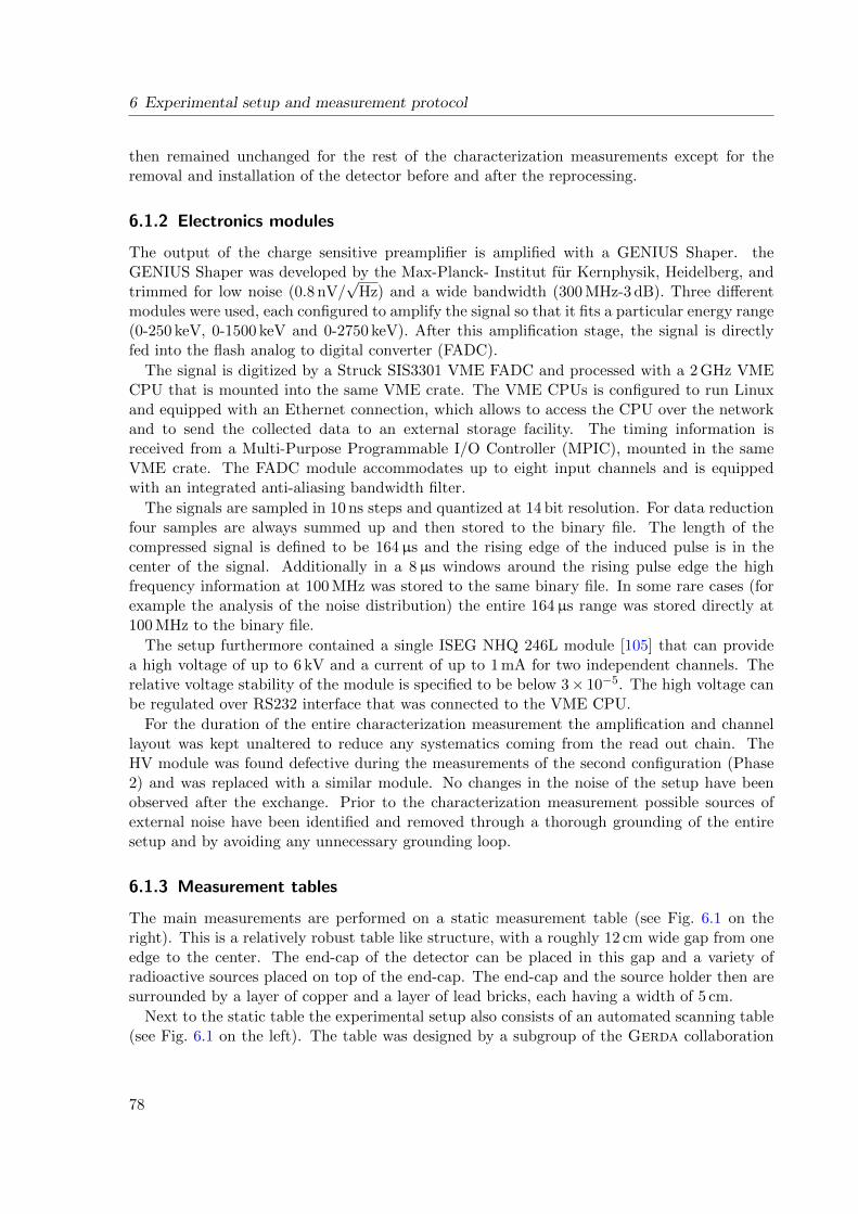
6 Experimental setup and measurement protocol
then remained unchanged for the rest of the characterization measurements except for theremoval and installation of the detector before and after the reprocessing.
6.1.2 Electronics modules
The output of the charge sensitive preamplifier is amplified with a GENIUS Shaper. theGENIUS Shaper was developed by the Max-Planck- Institut fur Kernphysik, Heidelberg, andtrimmed for low noise (0.8 nV/
√Hz) and a wide bandwidth (300 MHz-3 dB). Three different
modules were used, each configured to amplify the signal so that it fits a particular energy range(0-250 keV, 0-1500 keV and 0-2750 keV). After this amplification stage, the signal is directlyfed into the flash analog to digital converter (FADC).
The signal is digitized by a Struck SIS3301 VME FADC and processed with a 2 GHz VMECPU that is mounted into the same VME crate. The VME CPUs is configured to run Linuxand equipped with an Ethernet connection, which allows to access the CPU over the networkand to send the collected data to an external storage facility. The timing information isreceived from a Multi-Purpose Programmable I/O Controller (MPIC), mounted in the sameVME crate. The FADC module accommodates up to eight input channels and is equippedwith an integrated anti-aliasing bandwidth filter.
The signals are sampled in 10 ns steps and quantized at 14 bit resolution. For data reductionfour samples are always summed up and then stored to the binary file. The length of thecompressed signal is defined to be 164µs and the rising edge of the induced pulse is in thecenter of the signal. Additionally in a 8µs windows around the rising pulse edge the highfrequency information at 100 MHz was stored to the same binary file. In some rare cases (forexample the analysis of the noise distribution) the entire 164µs range was stored directly at100 MHz to the binary file.
The setup furthermore contained a single ISEG NHQ 246L module [105] that can providea high voltage of up to 6 kV and a current of up to 1 mA for two independent channels. Therelative voltage stability of the module is specified to be below 3× 10⁻⁵. The high voltage canbe regulated over RS232 interface that was connected to the VME CPU.
For the duration of the entire characterization measurement the amplification and channellayout was kept unaltered to reduce any systematics coming from the read out chain. TheHV module was found defective during the measurements of the second configuration (Phase2) and was replaced with a similar module. No changes in the noise of the setup have beenobserved after the exchange. Prior to the characterization measurement possible sources ofexternal noise have been identified and removed through a thorough grounding of the entiresetup and by avoiding any unnecessary grounding loop.
6.1.3 Measurement tables
The main measurements are performed on a static measurement table (see Fig. 6.1 on theright). This is a relatively robust table like structure, with a roughly 12 cm wide gap from oneedge to the center. The end-cap of the detector can be placed in this gap and a variety ofradioactive sources placed on top of the end-cap. The end-cap and the source holder then aresurrounded by a layer of copper and a layer of lead bricks, each having a width of 5 cm.
Next to the static table the experimental setup also consists of an automated scanning table(see Fig. 6.1 on the left). The table was designed by a subgroup of the Gerda collaboration
78
6.2 Measurement protocol
working at the University of Padova [106] and also used during the characterization measure-ments of the 30 new BEGe detectors in Belgium [63]. The scanning table is an automatedapparatus to perform surface scans. In these measurements a highly collimated 5 MBq 241Amsource (in our case with an hole diameter of 1 mm) is pointed at different locations on the sur-face of a detector. 241Am has one single line at 59.5 keV with a penetration depth of roughly1 mm in germanium and roughly 5 mm in Aluminum [44]. The γ-rays emitted by that sourcehave a good chance to penetrate through the aluminum end-cap but will be absorbed closeto the surface of the detector. Therefore only a very limited part of the detectors volume isexposed to the source, which for many applications can be assumed as almost point like. Thetable contains a movable arm that can be rotated between 0 and 359 and brought either in avertical or horizontal position depending on if the measured position is located on the top orside surface.
6.2 Measurement protocol
In this section the most important measurements performed for the characterization of the twodetectors are quickly discussed. The list however is not complete, additional measurementshave been performed for further analyses beyond this dissertation.
6.2.1 Source measurements
A set of radioactive sources have been organized to perform measurements with γ-ray lines atwell defined energies.
Single source measurements
The single source measurement have been all conducted on the static table. They use a singleradioactive isotope (except 228Th where also γ-ray lines from its decay chain are visible) thatproduces a single or multiple lines in the spectra. The time a measurement requires to be runand the distant at which the radioactive source is placed depends on its strength. The countrate should not be too large as it leads to more pile-ups and thus a worse energy resolutionbut also not too small as then the measurement takes a long time and the peaks might be lostin the background. A count rate between 100-300 Hz was found to be a good value for mostof the sources. The interesting peaks must at least contain 10’000 events to have a statisticaluncertainty of a minimum of 1%, thus the required measurement time with each source canbe estimated. Measurements have been performed with the following isotopes: 241Am, 133Ba,60Co and 228Th.
Mixed source measurements
To track the energy resolution over a large energy range it is beneficial to use a combinationof different sources that are placed such that the different peaks are roughly of equal height.A particular useful measurement was conducted with a mixture of 241Am, 133Ba, 134Cs, 137Cs,60Co, 152Eu and 228Th isotopes, which produce a spectrum with peaks in the entire energyrange between 59.5 keV and 2614.5 keV.
79
6 Experimental setup and measurement protocol
High voltage scans
The resolution in an undepleted detector is deteriorated compared to a fully depleted detectorand usually reaches an almost stable value once the depletion voltage is exceeded. To find thedepletion voltage, at a variety of bias voltages a γ-ray spectrum is measured and compared tothose measured at other voltages. The behavior as a function of the bias voltage was found tobe more stable if one reduces the bias voltage from a value above depletion voltage towardszero Volt. The measurement was performed once for 241Am and once for 60Co. The detectorsbias voltage was regulated from the operational voltage down to 500-1000 V in steps of 20 Vand each position has been measured for 5-10 min.
Surface scans with collimated 241Am source
The scanning table has been described in Sec. 6.1.3. It was decided on measuring a thin grid ofpoints along the surface. On the top surface the measurements have been taken along rings thatare aligned with the detectors center and separated by 2 mm distance. The average distancebetween two measurements in one ring also is 2 mm, so at small radii there are less pointstaken than at large radii. Along the side of the detector the measurements have been taken inrings at a specific height. The distance between measurement in the same ring is again 2 mm,the rings are separated by 4 mm distance.
The surface measurements allow to analyze in detail the signal shape from different locationsin the detector and estimate the drift time of the charge carriers. It has been shown for examplein Ref. [98] that such a measurement is sensitive to the anisotropic mobility of holes in thecrystal that was described in Sec. 4.4.2. Each point was measured for 5 min and in total therewere about 2000 points that needed to be measured for each detector.
6.2.2 Additional measurements
Some additional measurements have been performed that did not have the primary aim ofmeasuring any particular γ-ray line but some other effects and detector properties.
Pulser measurement
The most basic way to characterize the noise of an electronic circuit in radiation detectionsystems is to feed a fast rising pulser signal into the test input of the preamplifier system.The received output signal does not depend on the charge collection process, but only onthe rise time of the input pulse and the noise characteristics of the electronic circuitry. Themeasurement requires a very stable pulser signal at the test input, as small deviation in theheight of the input signal will deteriorate the measurement. It was performed with a HewlettPackard 8007B Pulse Generator with a 5 ns rise time.
Background measurements
The energy spectrum of the detector enclosed by an outer lead layer of 5 cm thickness and aninner layer of 5 cm copper was measured for 1-2 days. The trigger threshold was set into thenoise so that is was possible to observe the increased rate at low energies caused by accidentallytriggered noise fluctuations.
80
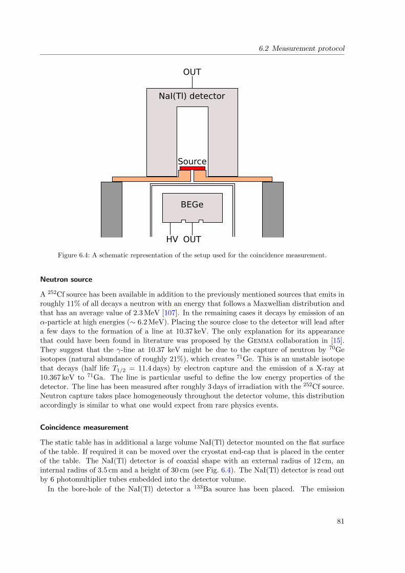
6.2 Measurement protocol
HV OUT
OUT
NaI(Tl) detector
BEGe
Source
Figure 6.4: A schematic representation of the setup used for the coincidence measurement.
Neutron source
A 252Cf source has been available in addition to the previously mentioned sources that emits inroughly 11% of all decays a neutron with an energy that follows a Maxwellian distribution andthat has an average value of 2.3 MeV [107]. In the remaining cases it decays by emission of anα-particle at high energies (∼ 6.2 MeV). Placing the source close to the detector will lead aftera few days to the formation of a line at 10.37 keV. The only explanation for its appearancethat could have been found in literature was proposed by the Gemma collaboration in [15].They suggest that the γ-line at 10.37 keV might be due to the capture of neutron by 70Geisotopes (natural abundance of roughly 21%), which creates 71Ge. This is an unstable isotopethat decays (half life T1/2 = 11.4 days) by electron capture and the emission of a X-ray at10.367 keV to 71Ga. The line is particular useful to define the low energy properties of thedetector. The line has been measured after roughly 3 days of irradiation with the 252Cf source.Neutron capture takes place homogeneously throughout the detector volume, this distributionaccordingly is similar to what one would expect from rare physics events.
Coincidence measurement
The static table has in additional a large volume NaI(Tl) detector mounted on the flat surfaceof the table. If required it can be moved over the cryostat end-cap that is placed in the centerof the table. The NaI(Tl) detector is of coaxial shape with an external radius of 12 cm, aninternal radius of 3.5 cm and a height of 30 cm (see Fig. 6.4). The NaI(Tl) detector is read outby 6 photomultiplier tubes embedded into the detector volume.
In the bore-hole of the NaI(Tl) detector a 133Ba source has been placed. The emission
81
6 Experimental setup and measurement protocol
of a 356.0 keV γ-ray from that isotope is always accompanied by an immediate emission ofan 81.0 keV γ-ray. This coincidental event can be exploited to better estimate the chargecollection time in a detector. The NaI(Tl) detector has a faster detector response than a typicalgermanium detector (in the range of 100 ns). Accordingly if the 356.0 keV γ-ray is measured inthe NaI(Tl) detector in coincident with a 81.0 keV γ-ray in the germanium detector the signalin the NaI(Tl) detector indicates the time of the energy deposition in the germanium detectorclose to the surface.
82
7 Investigation of filter performances
In order to achieve the best possible performance of a detector it is required to also useappropriate filtering methods. Unfortunately, there is no one-size-fits-all approach – the idealfilter parameters are strongly dependent on the data. In particular, the shaping filters mustmatch the characteristics of the data otherwise the quality of the results will be suboptimal.In the following chapter some of the most vital dependencies will be addressed. The resultswill be used in subsequent chapters to compare the different point contact sizes. Furthermore,a detailed knowledge of the filter characteristics allows a measurement of the Fano factor, animportant material property for many spectroscopy applications. This is done in the last partof this chapter.
7.1 Filter performance
A general expression for the equivalent noise charge was given in Eq. 4.20. Its form not onlydepends on the transfer function of the preamplifier but also the shaping filter that is used for itsevaluation. The lower limit in resolution could be found by minimizing the equation describingthe equivalent noise charge, however, in an experimental situation this solution rarely leadsto the best result. Effects, such as ballistic deficits and incomplete charge collection, are notdescribed within the framework of the equivalent noise charge. Thus the ideal choice of a filterstrongly depends on the data that are analyzed and how well the filter performs in the presenceof these effects.
Possible filter implementations have been proposed in Sec. 4.2. Most of these filters havenot yet been discussed in literature and prior to using them for an analysis their most vitaldependencies must be disentangled.
In order to analyze the impact of the various filter parameters, one particular measurementof Asterix in its Phase 2 configuration was selected. This measurement contains sufficient peaksin the energy range between 59.5 keV and 1460.8 keV.
7.1.1 Shaping time effects of the pseudo-Gaussian filter
The pseudo-Gaussian filter is commonly used in applications with γ-ray spectrometers and thuswill be used as a reference for the discussion about filter optimization. The pseudo-Gaussianfilter only has a single characteristic parameter – the shaping time. However, the filter can alsobe combined with the MSEC method described in Sec. 4.2.5. Therefore, a second parameteris introduced that defines if the MSEC method is enabled or not.
Fig. 7.1 illustrates how the resolution depends on the two parameters at 1332.5 keV. Theenergy resolution initially decreases with increasing shaping time, reaches a minimum andthen increases. This behavior is due to electronics noise that was expressed in Sec. 4.1.6 asthe equivalent noise charge. The equivalent noise charge is dominated by voltage noise at ashort shaping time and by current noise at a long shaping time. The optimum shaping timeis found at the position where the energy resolution is minimal and the two contributions are
83
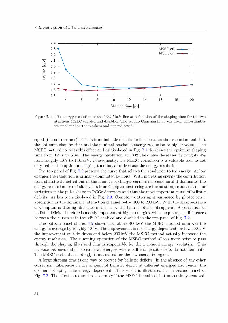
7 Investigation of filter performances
1.5
1.6
1.7
1.8
1.9
2.0
2.1
2.2
2.3
2.4
4 6 8 10 12 14 16 18 20
FW
HM
[keV
]
Shaping time [µs]
MSEC offMSEC on
Figure 7.1: The energy resolution of the 1332.5 keV line as a function of the shaping time for the twosituations MSEC enabled and disabled. The pseudo-Gaussian filter was used. Uncertaintiesare smaller than the markers and not indicated.
equal (the noise corner). Effects from ballistic deficits further broaden the resolution and shiftthe optimum shaping time and the minimal reachable energy resolution to higher values. TheMSEC method corrects this effect and as displayed in Fig. 7.1 decreases the optimum shapingtime from 12µs to 6µs. The energy resolution at 1332.5 keV also decreases by roughly 4%from roughly 1.67 to 1.61 keV. Consequently, the MSEC correction is a valuable tool to notonly reduce the optimum shaping time but also decrease the energy resolution.
The top panel of Fig. 7.2 presents the curve that relates the resolution to the energy. At lowenergies the resolution is primary dominated by noise. With increasing energy the contributionfrom statistical fluctuations in the number of charger carriers increases until it dominates theenergy resolution. Multi site events from Compton scattering are the most important reason forvariations in the pulse shape in PCGe detectors and thus the most important cause of ballisticdeficits. As has been displayed in Fig. 2.3, Compton scattering is surpassed by photoelectricabsorption as the dominant interaction channel below 100 to 200 keV. With the disappearanceof Compton scattering also effects caused by the ballistic deficit disappear. A correction ofballistic deficits therefore is mainly important at higher energies, which explains the differencesbetween the curves with the MSEC enabled and disabled in the top panel of Fig. 7.2.
The bottom panel of Fig. 7.2 shows that above 400 keV the MSEC method improves theenergy in average by roughly 50 eV. The improvement is not energy dependent. Below 400 keVthe improvement quickly drops and below 200 keV the MSEC method actually increases theenergy resolution. The summing operation of the MSEC method allows more noise to passthrough the shaping filter and thus is responsible for the increased energy resolution. Thisincrease becomes only noticeable at energies where ballistic deficit effects do not dominate.The MSEC method accordingly is not suited for the low energetic region.
A large shaping time is one way to correct for ballistic deficits. In the absence of any othercorrection, differences in the amount of ballistic deficit at different energies also render theoptimum shaping time energy dependent. This effect is illustrated in the second panel ofFig. 7.2. The effect is reduced considerably if the MSEC is enabled, but not entirely removed.
84
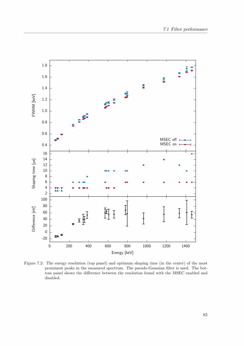
7.1 Filter performance
0.4
0.6
0.8
1.0
1.2
1.4
1.6
1.8
2
4
6
8
10
12
14
16
-20
0
20
40
60
80
100
0 200 400 600 800 1000 1200 1400
Energy [keV]
MSEC offMSEC on
FW
HM
[keV
]S
hap
ing
tim
e[µ
s]D
iffer
ence
[eV
]
Figure 7.2: The energy resolution (top panel) and optimum shaping time (in the center) of the mostprominent peaks in the measured spectrum. The pseudo-Gaussian filter is used. The bot-tom panel shows the difference between the resolution found with the MSEC enabled anddisabled.
85
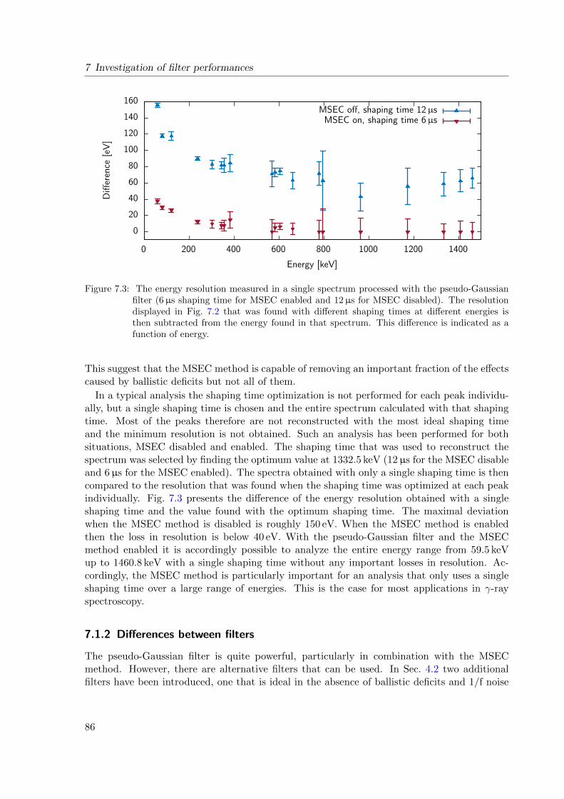
7 Investigation of filter performances
0
20
40
60
80
100
120
140
160
0 200 400 600 800 1000 1200 1400
Energy [keV]
MSEC off, shaping time 12µsMSEC on, shaping time 6µs
Diff
eren
ce[e
V]
Figure 7.3: The energy resolution measured in a single spectrum processed with the pseudo-Gaussianfilter (6µs shaping time for MSEC enabled and 12µs for MSEC disabled). The resolutiondisplayed in Fig. 7.2 that was found with different shaping times at different energies isthen subtracted from the energy found in that spectrum. This difference is indicated as afunction of energy.
This suggest that the MSEC method is capable of removing an important fraction of the effectscaused by ballistic deficits but not all of them.
In a typical analysis the shaping time optimization is not performed for each peak individu-ally, but a single shaping time is chosen and the entire spectrum calculated with that shapingtime. Most of the peaks therefore are not reconstructed with the most ideal shaping timeand the minimum resolution is not obtained. Such an analysis has been performed for bothsituations, MSEC disabled and enabled. The shaping time that was used to reconstruct thespectrum was selected by finding the optimum value at 1332.5 keV (12µs for the MSEC disableand 6µs for the MSEC enabled). The spectra obtained with only a single shaping time is thencompared to the resolution that was found when the shaping time was optimized at each peakindividually. Fig. 7.3 presents the difference of the energy resolution obtained with a singleshaping time and the value found with the optimum shaping time. The maximal deviationwhen the MSEC method is disabled is roughly 150 eV. When the MSEC method is enabledthen the loss in resolution is below 40 eV. With the pseudo-Gaussian filter and the MSECmethod enabled it is accordingly possible to analyze the entire energy range from 59.5 keVup to 1460.8 keV with a single shaping time without any important losses in resolution. Ac-cordingly, the MSEC method is particularly important for an analysis that only uses a singleshaping time over a large range of energies. This is the case for most applications in γ-rayspectroscopy.
7.1.2 Differences between filters
The pseudo-Gaussian filter is quite powerful, particularly in combination with the MSECmethod. However, there are alternative filters that can be used. In Sec. 4.2 two additionalfilters have been introduced, one that is ideal in the absence of ballistic deficits and 1/f noise
86
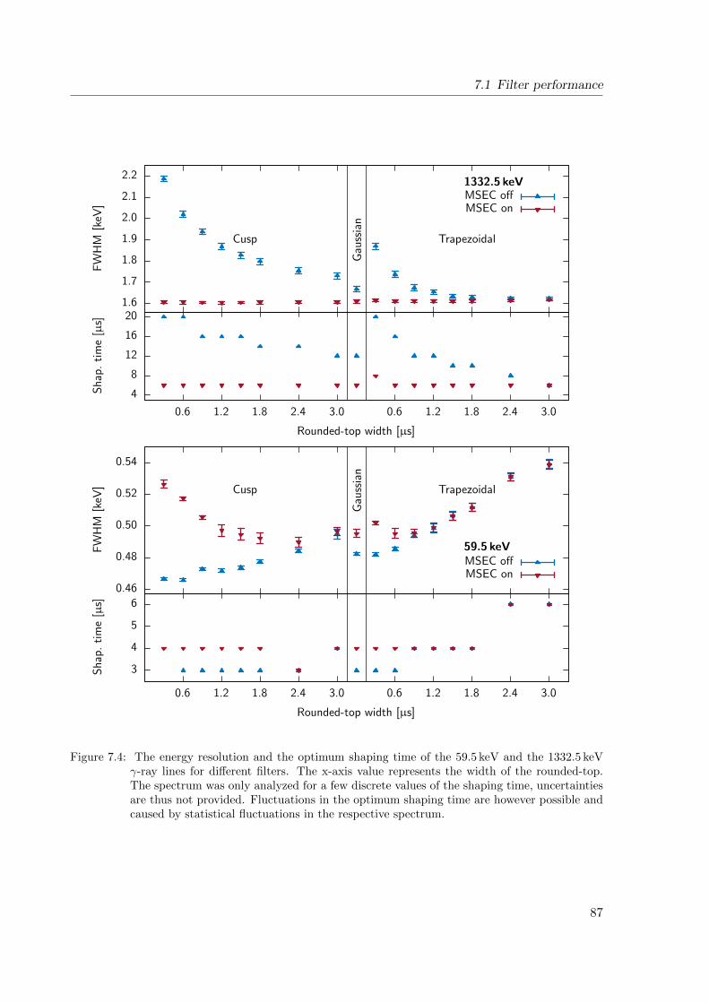
7.1 Filter performance
1.6
1.7
1.8
1.9
2.0
2.1
2.2
Gau
ssia
n
TrapezoidalCusp
1332.5 keV
4
8
12
16
20
0.6 1.2 1.8 2.4 3.0 0.6 1.2 1.8 2.4 3.0
Rounded-top width [µs]
MSEC offMSEC on
FW
HM
[keV
]S
hap
.ti
me
[µs]
0.46
0.48
0.50
0.52
0.54
Gau
ssia
n
TrapezoidalCusp
59.5 keV
3
4
5
6
0.6 1.2 1.8 2.4 3.0 0.6 1.2 1.8 2.4 3.0
Rounded-top width [µs]
MSEC offMSEC on
FW
HM
[keV
]S
hap
.ti
me
[µs]
Figure 7.4: The energy resolution and the optimum shaping time of the 59.5 keV and the 1332.5 keVγ-ray lines for different filters. The x-axis value represents the width of the rounded-top.The spectrum was only analyzed for a few discrete values of the shaping time, uncertaintiesare thus not provided. Fluctuations in the optimum shaping time are however possible andcaused by statistical fluctuations in the respective spectrum.
87
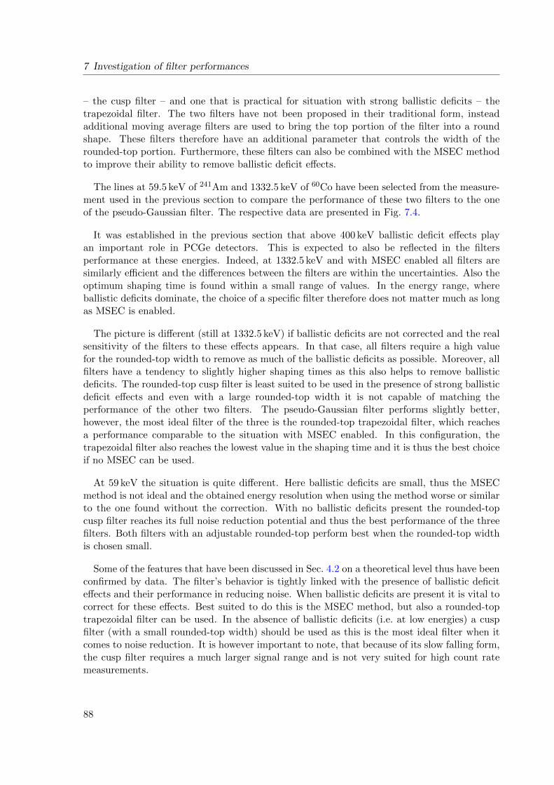
7 Investigation of filter performances
– the cusp filter – and one that is practical for situation with strong ballistic deficits – thetrapezoidal filter. The two filters have not been proposed in their traditional form, insteadadditional moving average filters are used to bring the top portion of the filter into a roundshape. These filters therefore have an additional parameter that controls the width of therounded-top portion. Furthermore, these filters can also be combined with the MSEC methodto improve their ability to remove ballistic deficit effects.
The lines at 59.5 keV of 241Am and 1332.5 keV of 60Co have been selected from the measure-ment used in the previous section to compare the performance of these two filters to the oneof the pseudo-Gaussian filter. The respective data are presented in Fig. 7.4.
It was established in the previous section that above 400 keV ballistic deficit effects playan important role in PCGe detectors. This is expected to also be reflected in the filtersperformance at these energies. Indeed, at 1332.5 keV and with MSEC enabled all filters aresimilarly efficient and the differences between the filters are within the uncertainties. Also theoptimum shaping time is found within a small range of values. In the energy range, whereballistic deficits dominate, the choice of a specific filter therefore does not matter much as longas MSEC is enabled.
The picture is different (still at 1332.5 keV) if ballistic deficits are not corrected and the realsensitivity of the filters to these effects appears. In that case, all filters require a high valuefor the rounded-top width to remove as much of the ballistic deficits as possible. Moreover, allfilters have a tendency to slightly higher shaping times as this also helps to remove ballisticdeficits. The rounded-top cusp filter is least suited to be used in the presence of strong ballisticdeficit effects and even with a large rounded-top width it is not capable of matching theperformance of the other two filters. The pseudo-Gaussian filter performs slightly better,however, the most ideal filter of the three is the rounded-top trapezoidal filter, which reachesa performance comparable to the situation with MSEC enabled. In this configuration, thetrapezoidal filter also reaches the lowest value in the shaping time and it is thus the best choiceif no MSEC can be used.
At 59 keV the situation is quite different. Here ballistic deficits are small, thus the MSECmethod is not ideal and the obtained energy resolution when using the method worse or similarto the one found without the correction. With no ballistic deficits present the rounded-topcusp filter reaches its full noise reduction potential and thus the best performance of the threefilters. Both filters with an adjustable rounded-top perform best when the rounded-top widthis chosen small.
Some of the features that have been discussed in Sec. 4.2 on a theoretical level thus have beenconfirmed by data. The filter’s behavior is tightly linked with the presence of ballistic deficiteffects and their performance in reducing noise. When ballistic deficits are present it is vital tocorrect for these effects. Best suited to do this is the MSEC method, but also a rounded-toptrapezoidal filter can be used. In the absence of ballistic deficits (i.e. at low energies) a cuspfilter (with a small rounded-top width) should be used as this is the most ideal filter when itcomes to noise reduction. It is however important to note, that because of its slow falling form,the cusp filter requires a much larger signal range and is not very suited for high count ratemeasurements.
88
7.1 Filter performance
1.58
1.60
1.62
1.64
1.66
1.68
1.70
1.721332.5 keV
68
10121416
0 2 4 6 8 10
Data compression (number of summed samples)
MSEC offMSEC on
FW
HM
[keV
]S
hap
.ti
me
[µs]
Figure 7.5: The effect of data compression on the energy resolution and optimum shaping time of the1332.5 keV γ-ray line. The compression value describes the number of samples that aresummed up prior to filtering.
compression 1 2 4 6 8 10initialization [hours:min] 02:47 01:42 01:10 01:07 01:09 01:02filtering [hours:min] 01:30 00:50 00:30 00:22 00:20 00:18filter rate [events/sec] 7002 12676 21048 27691 31385 34147data input [MB/sec] 67 121 200 264 299 325
Table 7.1: Benchmark of a typical analysis for different data compressions (compression of 1 meansuncompressed). Indicated are only the CPU (user) time, the system time (used for I/Ooperations) is compression independent and roughly 20 min for the initialization and 17 minfor the filtering. The size of the data set was roughly 355 GB which corresponds to 38 millionevents.
89
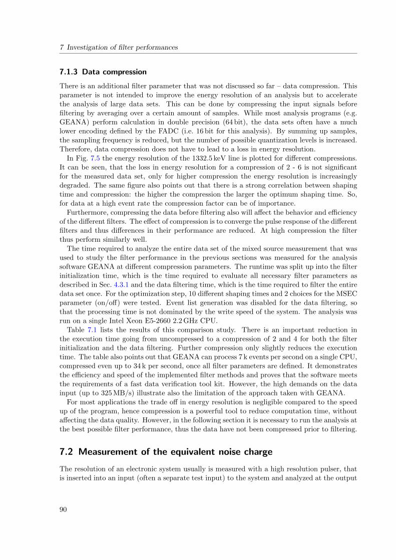
7 Investigation of filter performances
7.1.3 Data compression
There is an additional filter parameter that was not discussed so far – data compression. Thisparameter is not intended to improve the energy resolution of an analysis but to acceleratethe analysis of large data sets. This can be done by compressing the input signals beforefiltering by averaging over a certain amount of samples. While most analysis programs (e.g.GEANA) perform calculation in double precision (64 bit), the data sets often have a muchlower encoding defined by the FADC (i.e. 16 bit for this analysis). By summing up samples,the sampling frequency is reduced, but the number of possible quantization levels is increased.Therefore, data compression does not have to lead to a loss in energy resolution.
In Fig. 7.5 the energy resolution of the 1332.5 keV line is plotted for different compressions.It can be seen, that the loss in energy resolution for a compression of 2 - 6 is not significantfor the measured data set, only for higher compression the energy resolution is increasinglydegraded. The same figure also points out that there is a strong correlation between shapingtime and compression: the higher the compression the larger the optimum shaping time. So,for data at a high event rate the compression factor can be of importance.
Furthermore, compressing the data before filtering also will affect the behavior and efficiencyof the different filters. The effect of compression is to converge the pulse response of the differentfilters and thus differences in their performance are reduced. At high compression the filterthus perform similarly well.
The time required to analyze the entire data set of the mixed source measurement that wasused to study the filter performance in the previous sections was measured for the analysissoftware GEANA at different compression parameters. The runtime was split up into the filterinitialization time, which is the time required to evaluate all necessary filter parameters asdescribed in Sec. 4.3.1 and the data filtering time, which is the time required to filter the entiredata set once. For the optimization step, 10 different shaping times and 2 choices for the MSECparameter (on/off) were tested. Event list generation was disabled for the data filtering, sothat the processing time is not dominated by the write speed of the system. The analysis wasrun on a single Intel Xeon E5-2660 2.2 GHz CPU.
Table 7.1 lists the results of this comparison study. There is an important reduction inthe execution time going from uncompressed to a compression of 2 and 4 for both the filterinitialization and the data filtering. Further compression only slightly reduces the executiontime. The table also points out that GEANA can process 7 k events per second on a single CPU,compressed even up to 34 k per second, once all filter parameters are defined. It demonstratesthe efficiency and speed of the implemented filter methods and proves that the software meetsthe requirements of a fast data verification tool kit. However, the high demands on the datainput (up to 325 MB/s) illustrate also the limitation of the approach taken with GEANA.
For most applications the trade off in energy resolution is negligible compared to the speedup of the program, hence compression is a powerful tool to reduce computation time, withoutaffecting the data quality. However, in the following section it is necessary to run the analysis atthe best possible filter performance, thus the data have not been compressed prior to filtering.
7.2 Measurement of the equivalent noise charge
The resolution of an electronic system usually is measured with a high resolution pulser, thatis inserted into an input (often a separate test input) to the system and analyzed at the output
90
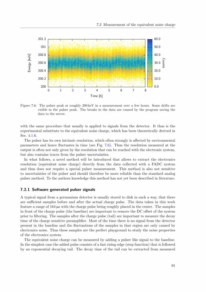
7.2 Measurement of the equivalent noise charge
Time [h]
En
ergy
[keV
]
200
200.2
200.4
200.6
200.8
201
201.2
0 1 2 3 4 5 6 7 80.0
10.0
20.0
30.0
40.0
50.0
60.0C
oun
ts
Figure 7.6: The pulser peak at roughly 200 keV in a measurement over a few hours. Some drifts arevisible in the pulser peak. The breaks in the data are caused by the program saving thedata to the server.
with the same procedure that usually is applied to signals from the detector. It thus is theexperimental substitute to the equivalent noise charge, which has been theoretically derived inSec. 4.1.6.
The pulser has its own intrinsic resolution, which often strongly is affected by environmentalparameters and hence fluctuates in time (see Fig. 7.6). Thus the resolution measured at theoutput is often not only given by the resolution that can be reached with the electronic system,but also contains traces from the pulser uncertainties.
In what follows, a novel method will be introduced that allows to extract the electronicsresolution (equivalent noise charge) directly from the data collected with a FADC systemand thus does not require a special pulser measurement. This method is also not sensitiveto uncertainties of the pulser and should therefore be more reliable than the standard analogpulser method. To the authors knowledge this method has not yet been described in literature.
7.2.1 Software generated pulser signals
A typical signal from a germanium detector is usually stored to disk in such a way, that thereare sufficient samples before and after the actual charge pulse. The data taken in this workfeature a range of 164µs with the charge pulse being roughly placed in the center. The samplesin front of the charge pulse (the baseline) are important to remove the DC offset of the systemprior to filtering. The samples after the charge pulse (tail) are important to measure the decaytime of the charge sensitive preamplifier. Most of the time there is no signal from the detectorpresent in the baseline and the fluctuations of the samples in that region are only caused byelectronics noise. Thus these samples are the perfect playground to study the noise propertiesof the electronics system.
The equivalent noise charge can be measured by adding a pulser like signal to the baseline.In the simplest case the added pulse consists of a fast rising edge (step function) that is followedby an exponential decaying tail. The decay time of the tail can be extracted from measured
91
7 Investigation of filter performances
320
340
360
380
400
420
64666870727476
2 3 4 5 6
Shaping time [µs]
Analog pulserSoftware pulser
FW
HM
[eV
]√ σ2 P
−σ2 S
[eV
]
Figure 7.7: The analog pulser (at the test input of the preamplifier) and the software generated pulsercompared at different shaping times. The most ideal filter at 59.5 keV has been used (cuspwith 0.3µs rounded-top width and MSEC disabled). The baseline is of the same length forboth the analog and software pulser. In the lower panel σS is the resolution of the simulationand σP of the pulser (FWHM). Uncertainties in the top panel are smaller than the markersand not indicated.
detector pulses and then used for the generation of a pulser like signal. This artificially createdpulser signal is then analyzed with the shaping filter in analogue to the signals measured fromthe detectors. The width of the peak that is observed in the spectrum due to this addedsignal corresponds to the equivalent noise charge of a given electronics system analyzed witha particular shaping filter.
This method can not give a realistic representation of nonlinearities of the system. Thepulser is only simulated at a single energy and thus only sensitive to a small region wherenonlinearities can be neglected.
7.2.2 Software versus analog generated pulser
The described method was applied to a measurement with an analog pulser (at roughly 200 keV)connected to the test input while the detector was irradiated with a 241Am source. A softwaregenerated pulse has been added to the baseline of the signals and the resulting resolutioncompared with the resolution from the pulser signal observed in the data. This can be seenin the top panel of Fig. 7.7 as a function of the shaping time. There is an offset betweenthe two measurements, however the lower panel in Fig. 7.7 shows that the offset is shapingtime independent and roughly 70 eV (0.04% of the pulse height) in size. In Fig. 7.6 it can beseen that there are some drifts in the pulser position of that measurement. The offset canbe easily explained by these fluctuations of the pulser. The value found by the method isaccordingly not affected by pulser drifts. Different filters and other data are in good agreement
92
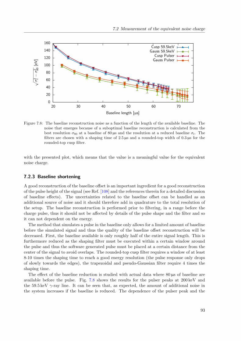
7.2 Measurement of the equivalent noise charge
0
20
40
60
80
100
120
140
160
20 30 40 50 60 70
√ σ2 t−σ2 80
[eV
]
Baseline length [µs]
Cusp 59.5keVGauss 59.5keV
Cusp PulserGauss Pulser
Figure 7.8: The baseline reconstruction noise as a function of the length of the available baseline. Thenoise that emerges because of a suboptimal baseline reconstruction is calculated from thebest resolution σ80 at a baseline of 80µs and the resolution at a reduced baseline σt. Thefilters are chosen with a shaping time of 2.5µs and a rounded-top width of 0.3µs for therounded-top cusp filter.
with the presented plot, which means that the value is a meaningful value for the equivalentnoise charge.
7.2.3 Baseline shortening
A good reconstruction of the baseline offset is an important ingredient for a good reconstructionof the pulse height of the signal (see Ref. [108] and the references therein for a detailed discussionof baseline effects). The uncertainties related to the baseline offset can be handled as anadditional source of noise and it should therefore add in quadrature to the total resolution ofthe setup. The baseline reconstruction is performed prior to filtering, in a range before thecharge pulse, thus it should not be affected by details of the pulse shape and the filter and soit can not dependent on the energy.
The method that simulates a pulse in the baseline only allows for a limited amount of baselinebefore the simulated signal and thus the quality of the baseline offset reconstruction will bedecreased. First, the baseline available is only roughly half of the entire signal length. This isfurthermore reduced as the shaping filter must be executed within a certain window aroundthe pulse and thus the software generated pulse must be placed at a certain distance from thecenter of the signal to avoid overlaps. The rounded-top cusp filter requires a window of at least8-10 times the shaping time to reach a good energy resolution (the pulse response only dropsof slowly towards the edges), the trapezoidal and pseudo-Gaussian filter require 4 times theshaping time.
The effect of the baseline reduction is studied with actual data where 80µs of baseline areavailable before the pulse. Fig. 7.8 shows the results for the pulser peaks at 200 keV andthe 59.5 keV γ-ray line. It can be seen that, as expected, the amount of additional noise inthe system increases if the baseline is reduced. The dependence of the pulser peak and the
93
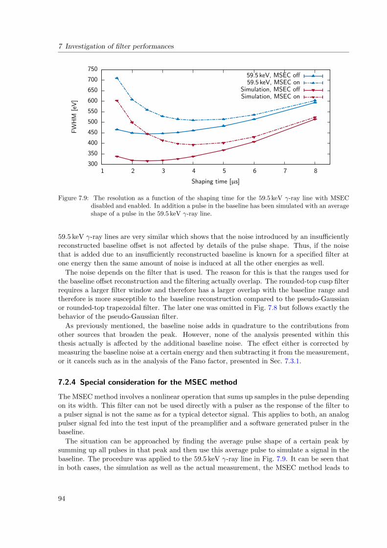
7 Investigation of filter performances
300
350
400
450
500
550
600
650
700
750
1 2 3 4 5 6 7 8
FW
HM
[eV
]
Shaping time [µs]
59.5 keV, MSEC off59.5 keV, MSEC on
Simulation, MSEC offSimulation, MSEC on
Figure 7.9: The resolution as a function of the shaping time for the 59.5 keV γ-ray line with MSECdisabled and enabled. In addition a pulse in the baseline has been simulated with an averageshape of a pulse in the 59.5 keV γ-ray line.
59.5 keV γ-ray lines are very similar which shows that the noise introduced by an insufficientlyreconstructed baseline offset is not affected by details of the pulse shape. Thus, if the noisethat is added due to an insufficiently reconstructed baseline is known for a specified filter atone energy then the same amount of noise is induced at all the other energies as well.
The noise depends on the filter that is used. The reason for this is that the ranges used forthe baseline offset reconstruction and the filtering actually overlap. The rounded-top cusp filterrequires a larger filter window and therefore has a larger overlap with the baseline range andtherefore is more susceptible to the baseline reconstruction compared to the pseudo-Gaussianor rounded-top trapezoidal filter. The later one was omitted in Fig. 7.8 but follows exactly thebehavior of the pseudo-Gaussian filter.
As previously mentioned, the baseline noise adds in quadrature to the contributions fromother sources that broaden the peak. However, none of the analysis presented within thisthesis actually is affected by the additional baseline noise. The effect either is corrected bymeasuring the baseline noise at a certain energy and then subtracting it from the measurement,or it cancels such as in the analysis of the Fano factor, presented in Sec. 7.3.1.
7.2.4 Special consideration for the MSEC method
The MSEC method involves a nonlinear operation that sums up samples in the pulse dependingon its width. This filter can not be used directly with a pulser as the response of the filter toa pulser signal is not the same as for a typical detector signal. This applies to both, an analogpulser signal fed into the test input of the preamplifier and a software generated pulser in thebaseline.
The situation can be approached by finding the average pulse shape of a certain peak bysumming up all pulses in that peak and then use this average pulse to simulate a signal in thebaseline. The procedure was applied to the 59.5 keV γ-ray line in Fig. 7.9. It can be seen thatin both cases, the simulation as well as the actual measurement, the MSEC method leads to
94
7.3 Fano factor
Croft [61] Lowe [109] Lepy [110] Papp [111] Wiens[112] Harkness [98]0.112± 0.001 0.1057± 0.0002 0.0953± 0.0005 0.05-0.082 0.095± 0.006 0.099
0.1084± 0.0008
Table 7.2: A few selected values for the Fano factor from recent measurements.
an increased resolution and a higher shaping time. This effect has been mentioned previouslyin Sec. 7.1.1 and is caused by the summing operation that is part of the MSEC algorithm.Fig. 7.9 shows that using the average pulse indeed reproduces roughly what has been observedfor the MSEC method enabled in the data. However, at low shaping times the simulated curveincreases faster than the data. This shows that an estimation of the equivalent noise chargeof an analysis with the MSEC enabled must be considered with care. Studies that involvean estimation of the equivalent noise charge (either coming from actual data or a simulation)should avoid the usage of the MSEC method.
7.3 Fano factor
Above about 100 keV the energy resolution of a PCGe detector is not dominated by noise butby charge carrier statistics and thus the Fano factor. It is therefore surprising that the exactvalue of the Fano factor in germanium still seems to be an open issue. In 1970 Zulliger [113]considered the matter as basically settled with theoretical models and experimental measure-ments converging on a value around 0.05. However, with the introduction of HPGe detectorsit became clear that the extrapolation to infinite charge collecting field conditions used bymany earlier authors underestimated the Fano factor. In 1991, Croft measured a value of 0.11and asked for more measurements to finally settle the matter [61]. However his call remainedmostly unheard. Only recently, the interest in the Fano factor has been revived and a fewnew studies [98, 110, 112] published that found values in agreement with Croft (see Table 7.2).However, there are also other authors that measured much lower values, particularly in theenergy region below 20 keV [111]. Some basic consideration about the origin of the Fano factorhave been discussed in Sec. 2.3.2. The intention of this section is to follow Crofts call for moremeasurements and use a few selected data of good quality to perform such an analysis.
7.3.1 Analysis procedure
Neglecting any loss in energy resolution that is due to incomplete charge collection, the Fanofactor is expressed as:
F =(σ2T − σ2
N )
Eε, (7.1)
where σT is the energy resolution (variance not FWHM) of a γ-ray line at an energy E and σNthe equivalent noise charge observed with the same filter configuration as used to measure theγ-ray line. The average energy required to create an electron-hole-pair ε has been measuredfor germanium and was found to be 2.96 eV, which will be used throughout this dissertation.
Eq. 7.1 states that to measure the Fano factor at a given energy it is required to know theequivalent noise charge at a given energy. Often an additional pulser measurement is used.However, it has been seen in the previous discussion that it can not be assured that the pulseris stable over a sufficiently long time scale. Thus it is more convenient to use the procedure
95
7 Investigation of filter performances
describe in Sec. 7.2 that finds the equivalent noise charge directly from a given data set, notrequiring a pulser being present. The equivalent noise charge must be calculated with thesame method that is also used for the analysis of the data. However, it only can make useof a restricted amount of the total baseline. Accordingly, the baseline of the measured datamust be restricted to the same length as the range available for the equivalent noise chargesimulation. The effect of a reduced baseline affects both, measurement and extraction of theequivalent noise charge in the same way. The effect accordingly cancels when calculating theFano factor.
Tailing effect in a peak are of different origin than the Fano factor (mostly from ballisticdeficit and incomplete charge collection). The tails should therefore not be included into theenergy resolution that is used for calculating the Fano factor. Instead the equation that hasbeen described in Sec. 4.2.7 is used for fitting the peaks and only the variance of the Gaussianterm taken for the analysis.
The evaluation of the Fano factor has been performed with the data set used in Sec. 7.1,however, was reduced to the most prominent γ-ray lines (more than 105 counts in the peak).Weak lines introduce strong uncertainties when it comes to the calculation of the Fano factor(because of the subtraction of two squared resolutions) and it is more reliable to exclude them.The entire data set has been processed for any possible combination of the pseudo-Gaussian,rounded-top cusp and trapezoidal filter (a selection of rounded-top width was used) and avariety of shaping times (2-14µs). The MSEC method was disabled. For each combinationof filter parameters the equivalent noise charge has been additionally found with the newprocedure outlined in Sec. 7.2 (software generated pulser). From Eq. 7.1 it is then possible tocalculate the Fano factor for a given γ-ray line.
7.3.2 Energy dependence of the Fano factor
The Fano factor is a constant defined by material properties and thus should not be dependenton the filter that is used for the energy reconstruction. Nonetheless, if the filter is not idealit will leave artifacts in the peak shape that must be disentangle from the contributions ofcharge carrier statistics. Particularly effects, such as ballistic deficits, that do not affect themeasurement of the equivalent noise charge in the same manner as the γ-ray line introducesystematic uncertainties. This problematic can be avoided by choosing a filter that reducesthese effects sufficiently so that they can be neglected. The filter with the lowest FWHM(including contributions from the tail) has therefore been chosen for each γ-ray line separatelyto be used in the measurement of the Fano factor. The minimization of the FWHM assuresthat the filter does neither produce strong tails nor a large variance in the peak.
The evaluation of the Fano factor depends on an exact measure of the equivalent noisecharge, thus the MSEC method should not be used and was disabled for the entire analysis.
The Fano factor as a function of energy is plotted in Fig. 7.10. There seems to be a slightenergy dependence, thus, a function of the form F (E) = A+B ·E was fitted to the data. Indeedthis fit is slightly better (χ2/dof = 4.6, with dof being the number of degrees of freedom) thanif the Fano factor is assumed to be a constant (χ2/dof = 4.7). The latter finds an value of0.1076± 0.0005 for the Fano factor.
An energy dependent Fano factor has previously been observed in silicon [62] but not yetbeen confirmed by other independent measurements. Moreover, in the absence of a good modelfor the physics behind the Fano factor such an dependence can not be excluded. Therefore, the
96
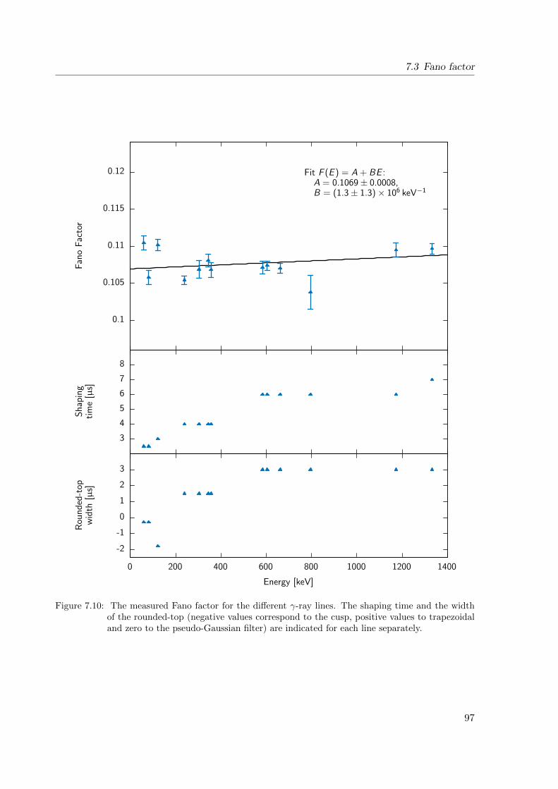
7.3 Fano factor
0.1
0.105
0.11
0.115
0.12 Fit F (E ) = A + BE :A = 0.1069± 0.0008,B = (1.3± 1.3)× 106 keV−1
3
4
5
6
7
8
-2
-1
0
1
2
3
0 200 400 600 800 1000 1200 1400
Energy [keV]
Fan
oF
acto
rS
hap
ing
tim
e[µ
s]R
oun
ded
-top
wid
th[µ
s]
Figure 7.10: The measured Fano factor for the different γ-ray lines. The shaping time and the widthof the rounded-top (negative values correspond to the cusp, positive values to trapezoidaland zero to the pseudo-Gaussian filter) are indicated for each line separately.
97
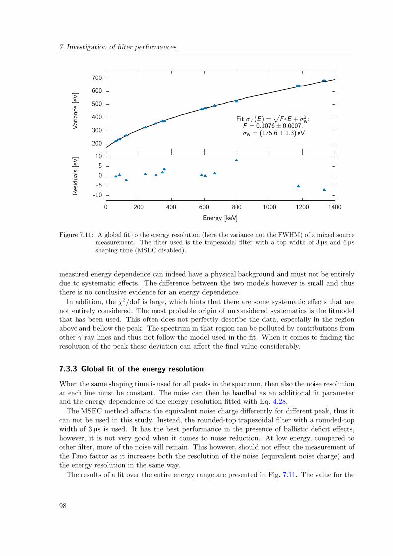
7 Investigation of filter performances
200
300
400
500
600
700
Fit σT (E ) =√
F εE + σ2N :
F = 0.1076± 0.0007,σN = (175.6± 1.3) eV
-10
-5
0
5
10
0 200 400 600 800 1000 1200 1400
Energy [keV]
Var
ian
ce[e
V]
Res
idu
als
[eV
]
Figure 7.11: A global fit to the energy resolution (here the variance not the FWHM) of a mixed sourcemeasurement. The filter used is the trapezoidal filter with a top width of 3µs and 6µsshaping time (MSEC disabled).
measured energy dependence can indeed have a physical background and must not be entirelydue to systematic effects. The difference between the two models however is small and thusthere is no conclusive evidence for an energy dependence.
In addition, the χ2/dof is large, which hints that there are some systematic effects that arenot entirely considered. The most probable origin of unconsidered systematics is the fitmodelthat has been used. This often does not perfectly describe the data, especially in the regionabove and bellow the peak. The spectrum in that region can be polluted by contributions fromother γ-ray lines and thus not follow the model used in the fit. When it comes to finding theresolution of the peak these deviation can affect the final value considerably.
7.3.3 Global fit of the energy resolution
When the same shaping time is used for all peaks in the spectrum, then also the noise resolutionat each line must be constant. The noise can then be handled as an additional fit parameterand the energy dependence of the energy resolution fitted with Eq. 4.28.
The MSEC method affects the equivalent noise charge differently for different peak, thus itcan not be used in this study. Instead, the rounded-top trapezoidal filter with a rounded-topwidth of 3µs is used. It has the best performance in the presence of ballistic deficit effects,however, it is not very good when it comes to noise reduction. At low energy, compared toother filter, more of the noise will remain. This however, should not effect the measurement ofthe Fano factor as it increases both the resolution of the noise (equivalent noise charge) andthe energy resolution in the same way.
The results of a fit over the entire energy range are presented in Fig. 7.11. The value for the
98
7.3 Fano factor
Fano factor of 0.1076± 0.0007 is identical to the value evaluated in the previous section. Theχ2/dof = 3.8 for the global fit is better as for the energy dependent fits. This measurementseems therefore to be less affected by certain systematics.
The presented study strongly suggests that a Fano factor close to the value found by Croftis most likely to be correct. Both method that have been presented found a value in goodagreement with each other and close to the value found by Croft. Although there is a hint thatthe Fano factor might be energy dependent the trend is not compatible with a value in therange around 0.05-0.08, even at very low energies. A possible explanation for the low values,particularly at low energies, found by some studies might be a pulser measurement with slightdrifts. If these effects are not carefully monitored it is easy to overestimate the pulser resolutionand thus find a much lower value for the Fano factor. This is particularly true at low energy,where the resolution is dominated by noise, not the Fano factor. In the energy range thathas been studied the contribution from statistical fluctuations in the number of charge carriersdominates. Thus, the a value found in that range is less prone to systematics.
99
8 Results from the point contact size study
This chapter will present the results from the characterization measurements of the two de-tectors – Asterix and Obelix – that were introduced in Sec. 5.2. These two detectors havebeen modified by changing the point contact size and the width of the groove. Asterix wascharacterized in three configurations, Obelix only in two. Some of the studied objects havebeen introduced in the previous chapter. The remaining topics will be briefly explained beforethe results on the different point contact sizes are presented.
8.1 Energy resolution
The energy resolution is one of the most important characteristics of a germanium detector. Asdiscussed in the previous chapter, at low energies electronics noise has an important impact onthe energy resolution. Thus, the reduction of the point contact size should also translate into animprovement in energy resolution. The resolution at high energies is dominated by statisticalfluctuations and not electronics noise. However, the size of the point contact is affecting thepulse shape and with changes in the pulse shape the intensity of ballistic deficits changes,thus introducing variations in the resolution. This effects are small, strong deviations betweendifferent point contact sizes therefore hint that the detector is not functioning properly.
This section discusses these aspect by comparing the energy resolution of the γ-ray line at59.5 keV of 241Am, the 1332.5 keV line of 60Co and the 2614.5 keV line of 228Th for the differentpoint contact sizes of the two detectors.
8.1.1 Low energy region (241Am)
It has been established that at 59.5 keV ballistic deficits are small and do not need to becorrected (see Sec. 7.1.1). Therefore, the MSEC method for the analysis of the 241Am datawas disabled. Furthermore, in Sec. 7.1 it was found that the rounded-top cusp filter with arounded-top width of 0.3µs performs best of all the presented filters. This filter was accordinglyselected for the analysis of the measurements presented in this section.
The optimum shaping time is fixed through the evaluation of the noise corner, the shapingtime at which the resolution takes the lowest value. The respective curves are shown in Fig. 8.1for the different detector configurations. The noise corner is shifted with each change inpoint contact size to a lower shaping time. This reflects a reduction in voltage noise whichdirectly is affected by the capacitance of the detector. The energy resolution improves for bothdetectors between the first and second configuration. The improvement is smaller after thelast reprocessing step of Asterix.
In Fig. 8.2 the shape of the 59.5 keV line in the up to three configuration is shown. Althoughimportant in number, on a logarithmic scale, the differences between the configurations arerelatively small. The peaks follow nearly a Gaussian distribution, however, in the secondand third configuration there are also small tailing contributions. The amplitude of the tail
100
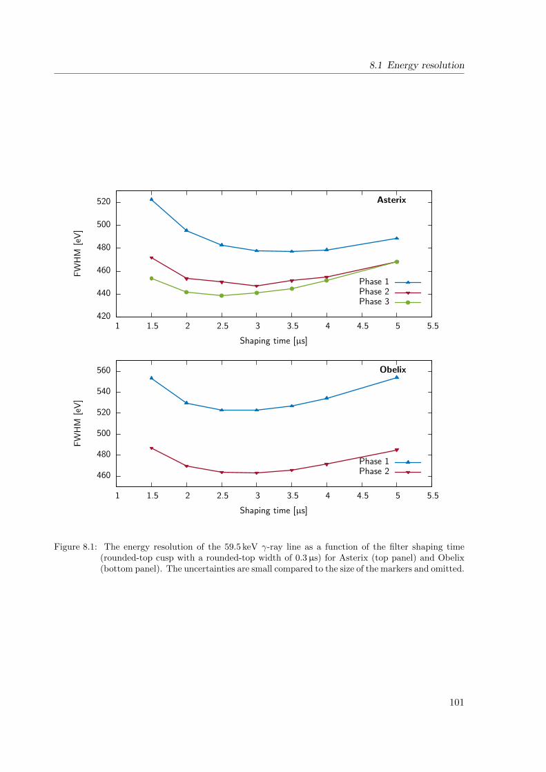
8.1 Energy resolution
420
440
460
480
500
520
1 1.5 2 2.5 3 3.5 4 4.5 5 5.5
FW
HM
[eV
]
Shaping time [µs]
Asterix
Phase 1Phase 2Phase 3
460
480
500
520
540
560
1 1.5 2 2.5 3 3.5 4 4.5 5 5.5
FW
HM
[eV
]
Shaping time [µs]
Obelix
Phase 1Phase 2
Figure 8.1: The energy resolution of the 59.5 keV γ-ray line as a function of the filter shaping time(rounded-top cusp with a rounded-top width of 0.3µs) for Asterix (top panel) and Obelix(bottom panel). The uncertainties are small compared to the size of the markers and omitted.
101
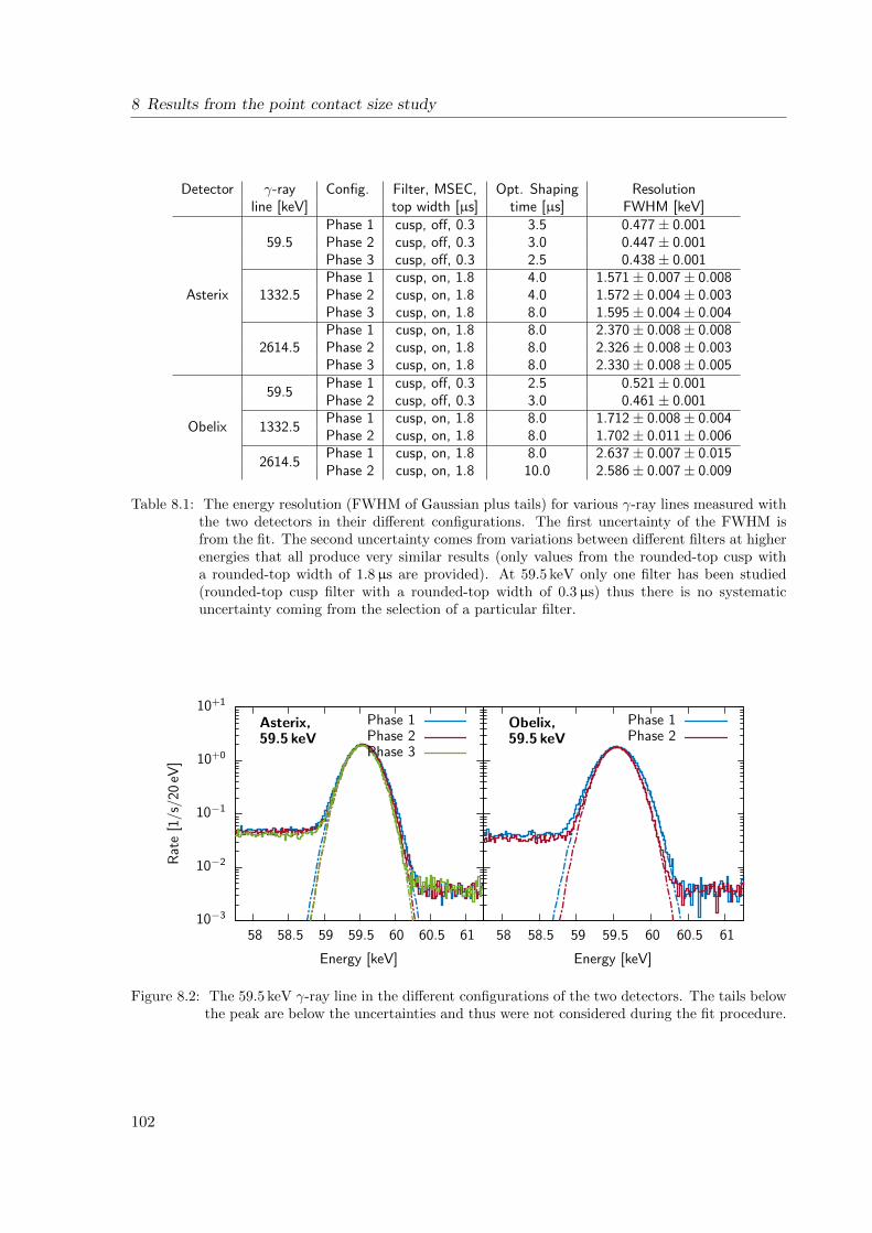
8 Results from the point contact size study
Detector γ-ray Config. Filter, MSEC, Opt. Shaping Resolutionline [keV] top width [µs] time [µs] FWHM [keV]
Asterix
59.5Phase 1 cusp, off, 0.3 3.5 0.477± 0.001Phase 2 cusp, off, 0.3 3.0 0.447± 0.001Phase 3 cusp, off, 0.3 2.5 0.438± 0.001
1332.5Phase 1 cusp, on, 1.8 4.0 1.571± 0.007± 0.008Phase 2 cusp, on, 1.8 4.0 1.572± 0.004± 0.003Phase 3 cusp, on, 1.8 8.0 1.595± 0.004± 0.004
2614.5Phase 1 cusp, on, 1.8 8.0 2.370± 0.008± 0.008Phase 2 cusp, on, 1.8 8.0 2.326± 0.008± 0.003Phase 3 cusp, on, 1.8 8.0 2.330± 0.008± 0.005
Obelix
59.5Phase 1 cusp, off, 0.3 2.5 0.521± 0.001Phase 2 cusp, off, 0.3 3.0 0.461± 0.001
1332.5Phase 1 cusp, on, 1.8 8.0 1.712± 0.008± 0.004Phase 2 cusp, on, 1.8 8.0 1.702± 0.011± 0.006
2614.5Phase 1 cusp, on, 1.8 8.0 2.637± 0.007± 0.015Phase 2 cusp, on, 1.8 10.0 2.586± 0.007± 0.009
Table 8.1: The energy resolution (FWHM of Gaussian plus tails) for various γ-ray lines measured withthe two detectors in their different configurations. The first uncertainty of the FWHM isfrom the fit. The second uncertainty comes from variations between different filters at higherenergies that all produce very similar results (only values from the rounded-top cusp witha rounded-top width of 1.8µs are provided). At 59.5 keV only one filter has been studied(rounded-top cusp filter with a rounded-top width of 0.3µs) thus there is no systematicuncertainty coming from the selection of a particular filter.
10−3
10−2
10−1
10+0
10+1
58 58.5 59 59.5 60 60.5 61
Rat
e[1
/s/2
0eV
]
Energy [keV]
Asterix,59.5 keV
58 58.5 59 59.5 60 60.5 61
Energy [keV]
Obelix,59.5 keV
Phase 1Phase 2Phase 3
Phase 1Phase 2
Figure 8.2: The 59.5 keV γ-ray line in the different configurations of the two detectors. The tails belowthe peak are below the uncertainties and thus were not considered during the fit procedure.
102
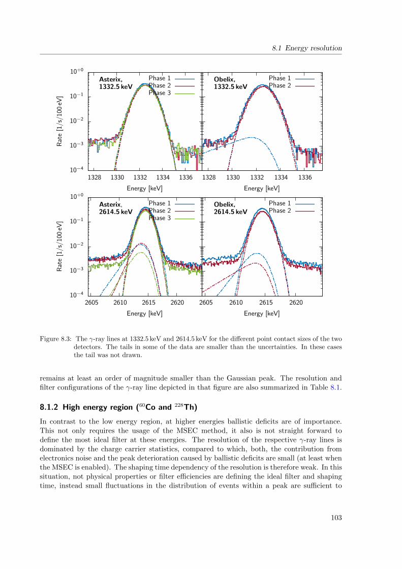
8.1 Energy resolution
10−4
10−3
10−2
10−1
10+0
1328 1330 1332 1334 1336
Rat
e[1
/s/1
00eV
]
Energy [keV]
Asterix,1332.5 keV
1328 1330 1332 1334 1336
Energy [keV]
Obelix,1332.5 keV
Phase 1Phase 2Phase 3
Phase 1Phase 2
10−4
10−3
10−2
10−1
10+0
2605 2610 2615 2620
Rat
e[1
/s/1
00eV
]
Energy [keV]
Asterix,2614.5 keV
2605 2610 2615 2620
Energy [keV]
Obelix,2614.5 keV
Phase 1Phase 2Phase 3
Phase 1Phase 2
Figure 8.3: The γ-ray lines at 1332.5 keV and 2614.5 keV for the different point contact sizes of the twodetectors. The tails in some of the data are smaller than the uncertainties. In these casesthe tail was not drawn.
remains at least an order of magnitude smaller than the Gaussian peak. The resolution andfilter configurations of the γ-ray line depicted in that figure are also summarized in Table 8.1.
8.1.2 High energy region (60Co and 228Th)
In contrast to the low energy region, at higher energies ballistic deficits are of importance.This not only requires the usage of the MSEC method, it also is not straight forward todefine the most ideal filter at these energies. The resolution of the respective γ-ray lines isdominated by the charge carrier statistics, compared to which, both, the contribution fromelectronics noise and the peak deterioration caused by ballistic deficits are small (at least whenthe MSEC is enabled). The shaping time dependency of the resolution is therefore weak. In thissituation, not physical properties or filter efficiencies are defining the ideal filter and shapingtime, instead small fluctuations in the distribution of events within a peak are sufficient to
103
8 Results from the point contact size study
favor one configuration over another.In order to process the 60Co and 228Th data the rounded-cusp filter with a rounded-top
width of 1.8µs was selected. All filters perform similar, hence this choice is rather arbitraryand might be better for a certain detector configuration than for another. The data are alsoprocessed with 6 other filters to calculate the variation between the different filters. Thisnumber is provided as a systematic uncertainty that describes the bias introduced by selectinga particular filter instead of the optimum one for each configuration. These uncertainties areindicated in Table 8.1 in addition to the uncertainties from the fit and are of the same orderof magnitude. The shaping time of each filter was selected by searching the noise corner.
At high energies, the resolution improves slightly when moving from the first to the secondconfiguration. The capacitance should only affect the electronics noise, which is a small contri-bution to the resolution at high energies, therefore this small improvement is predicted. Unex-pected is the behavior of Asterix at its third point contact size. The resolution at 1332.5 keVis deteriorated with respect to the second point contact size while it remains constant at2614.5 keV. It is not clear what the cause for this observation might be. Although great careis given to exclude systematic uncertainties coming from the experimental setup it is hardlypossible to exclude them to this level of precision. The effect, however, seems to be consistentand not only is observed in different measurements but also for three lines in the 228Th mea-surement that are in close proximity to the 1332.5 keV 60Co γ-ray line: the 1620.7 keV line of212Bi, the DEP at 1592.5 keV of 208Tl and the 1460.8 keV γ-ray line of 40K. If an understandingof the increased resolution of these γ-rays is crucial to the operation of such a detector in acertain experiment further investigation would be necessary, however, this is not the case here.
Fig. 8.3 presents the peak shape of the 1332.5 keV and 2614.5 keV lines for the two detectors.None of the configurations has important tailing, the tails described by the hypermet function(see Sec. 4.2.7) is usually one to two order of magnitude smaller than the Gaussian part of thefit. Thus, neither incomplete charge collection nor ballistic deficit effects strongly impact thepeak shape at any of the studied energies.
8.2 Equivalent noise charge
It has been shown that the equivalent noise charge depends on the shaping time and that fora low shaping time the voltage noise and for a high shaping time the current noise dominates.A method to measure the equivalent noise charge has been outlined in Sec. 7.2. The method isnow used to extract the different noise contributions that are present in measurements of thedetectors with different point contact sizes.
8.2.1 Shaping time dependency
Three measurements of a similar length (1 h) with a single 241Am source at 15 cm distance fromthe cryostat’s end cap and a dynamic range of 250 keV have been selected for this analysis.The data have been processed for a variety of shaping times (0.6-7.0µs) once with a rangeadopted so that a pulser could have been generated in software in the baseline, and once withthe normal range and no simulation of a pulser in the baseline. When a pulser is simulated inthe baseline then filters with a large shaping time have to use a small window to reconstructthe baseline which creates additional noise (see Sec. 7.2.3). The two different analysis, one witha long and one with a reduced baseline, allow to extract the additional baseline reconstruction
104
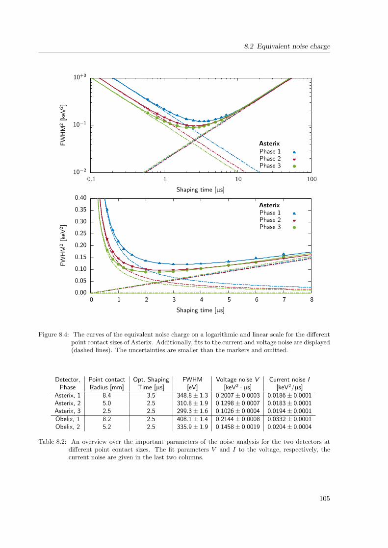
8.2 Equivalent noise charge
10−2
10−1
10+0
0.1 1 10 100
FW
HM
2[k
eV2]
Shaping time [µs]
AsterixPhase 1Phase 2Phase 3
0.00
0.05
0.10
0.15
0.20
0.25
0.30
0.35
0.40
0 1 2 3 4 5 6 7 8
FW
HM
2[k
eV2]
Shaping time [µs]
AsterixPhase 1Phase 2Phase 3
Figure 8.4: The curves of the equivalent noise charge on a logarithmic and linear scale for the differentpoint contact sizes of Asterix. Additionally, fits to the current and voltage noise are displayed(dashed lines). The uncertainties are smaller than the markers and omitted.
Detector, Point contact Opt. Shaping FWHM Voltage noise V Current noise IPhase Radius [mm] Time [µs] [eV] [keV2 · µs] [keV2/µs]
Asterix, 1 8.4 3.5 348.8± 1.3 0.2007± 0.0003 0.0186± 0.0001Asterix, 2 5.0 2.5 310.8± 1.9 0.1298± 0.0007 0.0183± 0.0001Asterix, 3 2.5 2.5 299.3± 1.6 0.1026± 0.0004 0.0194± 0.0001Obelix, 1 8.2 2.5 408.1± 1.4 0.2144± 0.0008 0.0332± 0.0001Obelix, 2 5.2 2.5 335.9± 1.9 0.1458± 0.0019 0.0204± 0.0004
Table 8.2: An overview over the important parameters of the noise analysis for the two detectors atdifferent point contact sizes. The fit parameters V and I to the voltage, respectively, thecurrent noise are given in the last two columns.
105
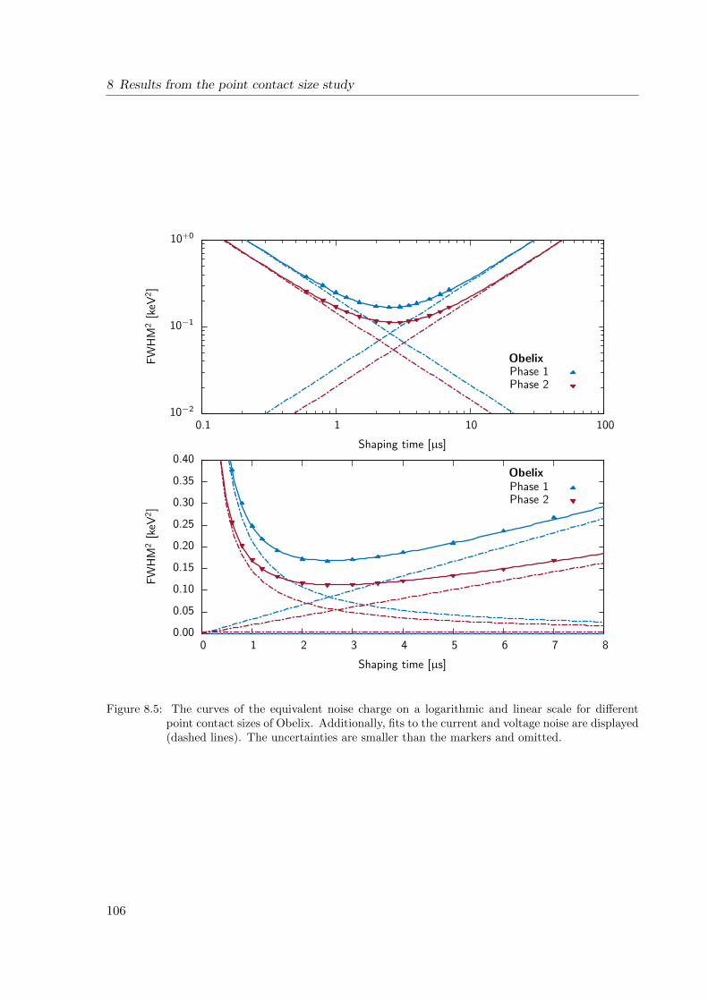
8 Results from the point contact size study
10−2
10−1
10+0
0.1 1 10 100
FW
HM
2[k
eV2]
Shaping time [µs]
ObelixPhase 1Phase 2
0.00
0.05
0.10
0.15
0.20
0.25
0.30
0.35
0.40
0 1 2 3 4 5 6 7 8
FW
HM
2[k
eV2]
Shaping time [µs]
ObelixPhase 1Phase 2
Figure 8.5: The curves of the equivalent noise charge on a logarithmic and linear scale for differentpoint contact sizes of Obelix. Additionally, fits to the current and voltage noise are displayed(dashed lines). The uncertainties are smaller than the markers and omitted.
106
8.2 Equivalent noise charge
Detector, Radius Leakage current [pA]Phase [cm] Canberra Fit
Asterix, 1 0.84 20 29.4± 0.1Asterix, 2 0.50 10-20 28.8± 0.2Asterix, 3 0.25 10-20 30.9± 0.2Obelix, 1 0.82 50-60 55.5± 0.2Obeliix, 2 0.52 10-20 32.6± 0.7
Table 8.3: A comparison between the leakage current extracted from the fit (assuming a 5 GΩ feedbackresistor at 110 K and Fi = 1 for an infinite cusp filter) and the values measured by Canberrawith a picoampermeter.
noise from the 59.5 keV γ-ray line. This noise can then be subtracted in quadrature from thepulser simulation to find a corrected estimation of the equivalent noise charge.
Fig. 8.4 and Fig. 8.5 present the outcome of this procedure for the three configurations ofAsterix and two configurations of Obelix, respectively. As expected, the reduction of the pointcontact size improves the noise resolution. Furthermore, the noise corner is shifted to lowershaping times with decreasing capacitance. The resolution at the noise corner and the optimumshaping time are indicated in Table 8.2. For both detectors the value of the equivalent noisecharge continuously improves when the point contact size is reduced. The best equivalent noisecharge obtained is roughly 300 eV at the smallest point contact size of Asterix. This value isroughly 20% better than the manufacture’s specifications of the preamplifier system.
8.2.2 Behavior of the voltage and current
The dependency of the noise resolution on the shaping time has been fitted with a function ofthe form:
Q2(Ts) =V
Ts+ I · Ts +A (8.1)
This formula follows Eq. 4.20 with the fitting variables corresponding to the voltage noiseV = e2
nFeC2tot and the current noise I = i2nFi at the shaping filters output. The 1/f noise has
been found negligible in any of the fits and thus A was set to zero. The values found for thesetwo variables in the fitting procedure are listed in Table 8.2.
The electronics setup has not be altered in the different configuration, thus the only valuethat is allowed to be changed must be related to the detector capacitance. Next to the 1/fnoise which has been neglected only the voltage noise is affected by the detector capacitance.The voltage noise is proportional to the square of the sum of the capacitances in the electronicscircuit C2
tot and thus with a reduction of the point contact size also the voltage noise is expectedto be lowered. This behavior indeed can be observed for both detectors after the point contactsize has been altered.
The entire surface between the two electrodes was refurbished in the process of changingthe size of the point contact. This area is the most probable origin of leakage currents andthus any alteration of the point contact changes leakage currents. Together with the feedbackresistor, leakage currents contribute to the current noise. The current noise thus is also affectedby the reprocessing of the detector. According to Canberra the feedback resistor is 5 GΩ andkept at roughly 110 K, thus it is possible to calculate the leakage current from the fit. Therespective values (see Table 8.3) agree reasonably well with the measurement conducted by
107
8 Results from the point contact size study
Canberra before shipping the detectors. The fit to the current noise for Asterix suggests thatthe current noise was reduced with the first reprocessing and then increased with the secondreprocessing, however, the differences are relatively small. On the contrary, after reprocessingObelix the current noise is reduced considerably. Obelix started with a relative high currentnoise and approached in the second configuration what was previously observed for Asterix.Still, the current noise in Obelix remained slightly worse, than what have been observed in anyconfiguration of Asterix. Overall, the observed leakage currents are rather on the high side andcurrently the limiting contribution to the current noise. This must be taken into considerationto improve the resolution any further and might actually require some considerable efforts suchas another rework of the groove.
The voltage noise at the output of the shaping filter is proportional to the square of thesum of the capacitances. Furthermore, the total shunt capacitance can be split up into thecontributions from the detector and other capacitance in parallel to the detector Ctot = Cd+Cp.The reduction of the contact size only affects the detector’s capacitance Cd while the sum ofthe remaining capacitance Cp is constant. Although the total voltage noise can be found fromthe fit for each detector geometry, it is not possible to entangle the multiplication factors e2
nFeand the two shunt capacitances Cd + Cp without any assumptions. A relation between thedetector capacitance and the point contact radius has been provided in Eq. 3.1. If we assumethat this form is correct for the two detectors, then the voltage noise can be expressed as:
V = e2nFe (Cp + 2πε0εrr)
2 , e2n =
8kT
3gm, (8.2)
where r is the radius of the point contact. The shaping factor Fe can be calculated from theimpulse response of the shaping filter. Its value is 1 for the infinite cusp which should beclose to the filter used in this analysis. The equation does not include the conversion factorsrequired between V and en which can be derived from the definition of the equivalent noisecharge. Thus the equation consists of two free parameters, so if at least two configurations ofthe point contact size have been measured then the system of equations is determined and theindividual values can be calculated. A fit of this function to the point contact sizes at whichthe current noise was evaluated is shown in Fig. 8.6 for Asterix. Only two data points areavailable for Obelix, the displayed curve corresponds to a simple calculation of the two freevariables and no uncertainties are provided. In both cases, the value for Cp is larger than whatis expected from just the feedback capacitance (according to Canberra Cf = 0.5 pF). On theother side, the value for the transconductance gm of the order of 10 mS indeed is in the typicalrange of a FET.
Next to this model it was also tested if it would be more accurate to assume the pointcontact detector as a parallel plate capacitor. In that case the capacitance is related to theradius through:
C =ε0εrπr
2
d, (8.3)
where d is the separation of the two plates in the parallel plate capacitor. In order to testthis model a certain value for the transconductance needs to be assumed. For simplicity thevalue found by the first model was used. The fit of this model to the data points of Asterix inFig. 8.6 is a more accurate description of the observed curves. The value for Cp, however, is ofthe same magnitude as what was found by the first model. Still, this shows that the studied
108
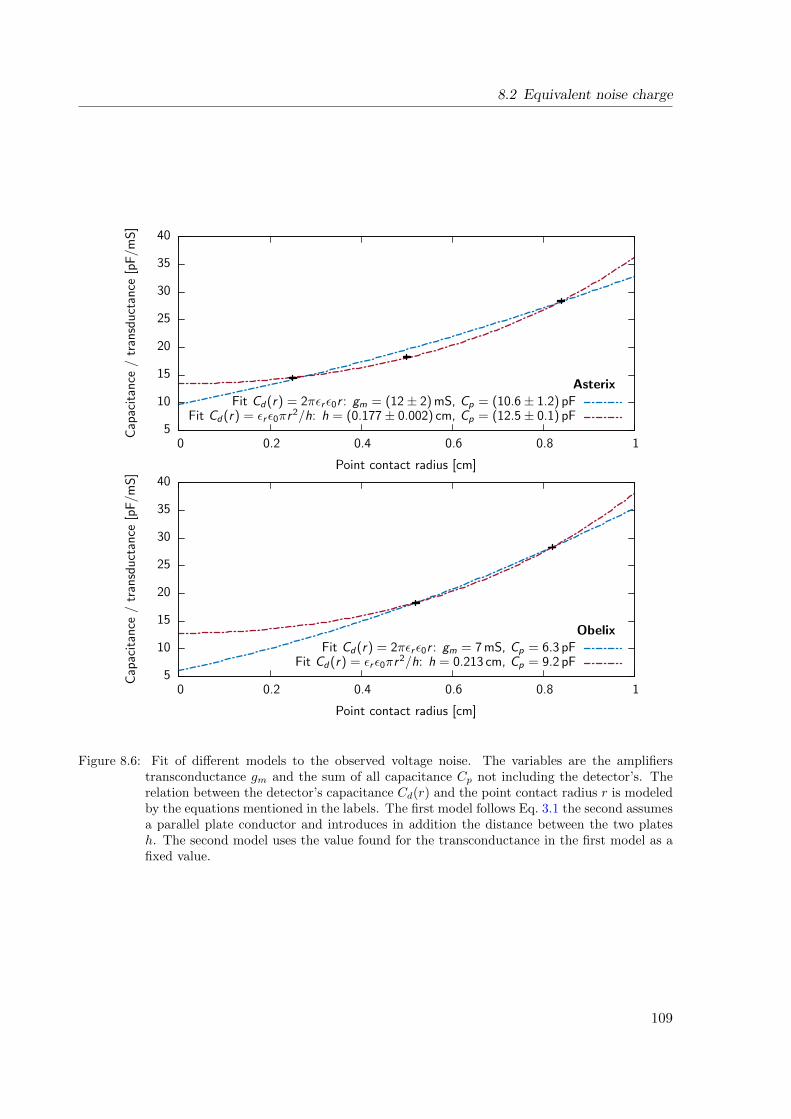
8.2 Equivalent noise charge
5
10
15
20
25
30
35
40
0 0.2 0.4 0.6 0.8 1
Cap
acit
ance
/tr
ansd
uct
ance
[pF
/mS
]
Point contact radius [cm]
AsterixFit Cd(r) = 2πεr ε0r : gm = (12± 2) mS, Cp = (10.6± 1.2) pF
Fit Cd(r) = εr ε0πr2/h: h = (0.177± 0.002) cm, Cp = (12.5± 0.1) pF
5
10
15
20
25
30
35
40
0 0.2 0.4 0.6 0.8 1
Cap
acit
ance
/tr
ansd
uct
ance
[pF
/mS
]
Point contact radius [cm]
ObelixFit Cd(r) = 2πεr ε0r : gm = 7 mS, Cp = 6.3 pF
Fit Cd(r) = εr ε0πr2/h: h = 0.213 cm, Cp = 9.2 pF
Figure 8.6: Fit of different models to the observed voltage noise. The variables are the amplifierstransconductance gm and the sum of all capacitance Cp not including the detector’s. Therelation between the detector’s capacitance Cd(r) and the point contact radius r is modeledby the equations mentioned in the labels. The first model follows Eq. 3.1 the second assumesa parallel plate conductor and introduces in addition the distance between the two platesh. The second model uses the value found for the transconductance in the first model as afixed value.
109
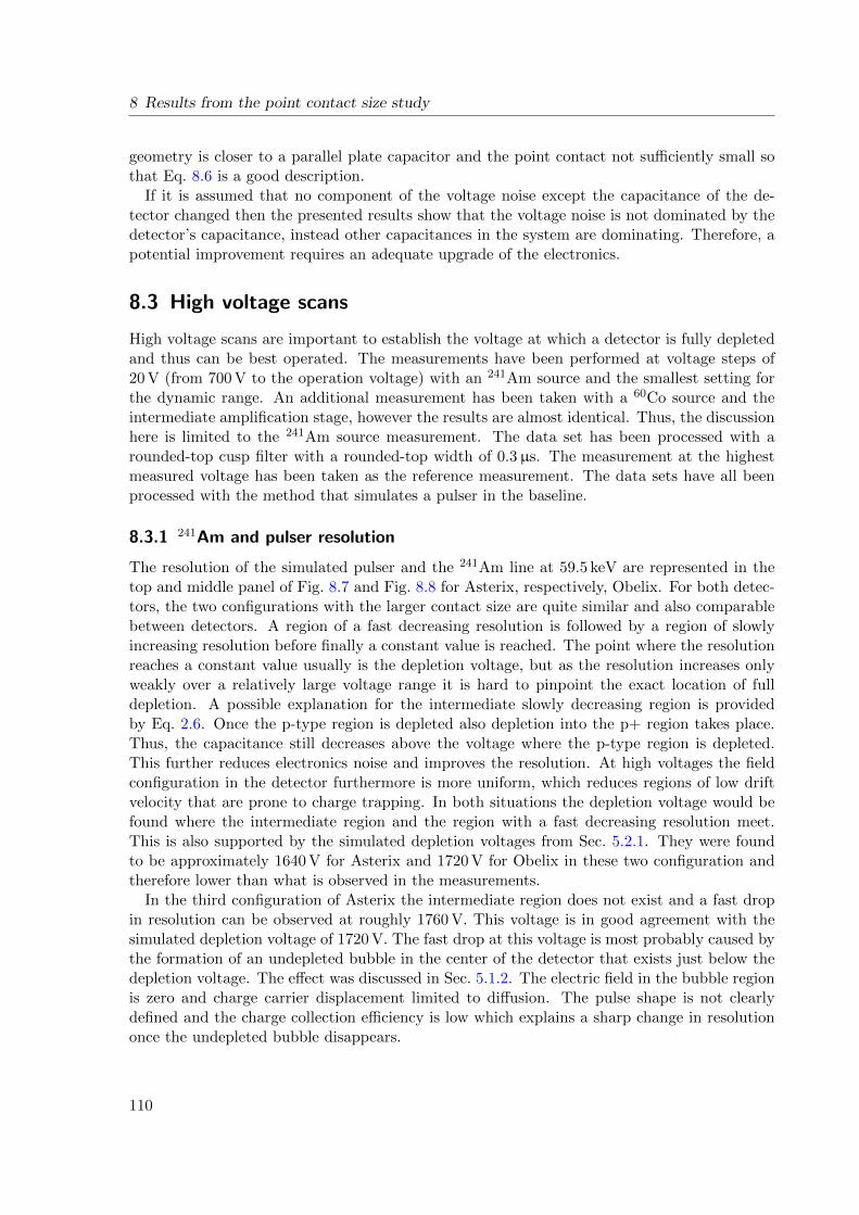
8 Results from the point contact size study
geometry is closer to a parallel plate capacitor and the point contact not sufficiently small sothat Eq. 8.6 is a good description.
If it is assumed that no component of the voltage noise except the capacitance of the de-tector changed then the presented results show that the voltage noise is not dominated by thedetector’s capacitance, instead other capacitances in the system are dominating. Therefore, apotential improvement requires an adequate upgrade of the electronics.
8.3 High voltage scans
High voltage scans are important to establish the voltage at which a detector is fully depletedand thus can be best operated. The measurements have been performed at voltage steps of20 V (from 700 V to the operation voltage) with an 241Am source and the smallest setting forthe dynamic range. An additional measurement has been taken with a 60Co source and theintermediate amplification stage, however the results are almost identical. Thus, the discussionhere is limited to the 241Am source measurement. The data set has been processed with arounded-top cusp filter with a rounded-top width of 0.3µs. The measurement at the highestmeasured voltage has been taken as the reference measurement. The data sets have all beenprocessed with the method that simulates a pulser in the baseline.
8.3.1 241Am and pulser resolution
The resolution of the simulated pulser and the 241Am line at 59.5 keV are represented in thetop and middle panel of Fig. 8.7 and Fig. 8.8 for Asterix, respectively, Obelix. For both detec-tors, the two configurations with the larger contact size are quite similar and also comparablebetween detectors. A region of a fast decreasing resolution is followed by a region of slowlyincreasing resolution before finally a constant value is reached. The point where the resolutionreaches a constant value usually is the depletion voltage, but as the resolution increases onlyweakly over a relatively large voltage range it is hard to pinpoint the exact location of fulldepletion. A possible explanation for the intermediate slowly decreasing region is providedby Eq. 2.6. Once the p-type region is depleted also depletion into the p+ region takes place.Thus, the capacitance still decreases above the voltage where the p-type region is depleted.This further reduces electronics noise and improves the resolution. At high voltages the fieldconfiguration in the detector furthermore is more uniform, which reduces regions of low driftvelocity that are prone to charge trapping. In both situations the depletion voltage would befound where the intermediate region and the region with a fast decreasing resolution meet.This is also supported by the simulated depletion voltages from Sec. 5.2.1. They were foundto be approximately 1640 V for Asterix and 1720 V for Obelix in these two configuration andtherefore lower than what is observed in the measurements.
In the third configuration of Asterix the intermediate region does not exist and a fast dropin resolution can be observed at roughly 1760 V. This voltage is in good agreement with thesimulated depletion voltage of 1720 V. The fast drop at this voltage is most probably caused bythe formation of an undepleted bubble in the center of the detector that exists just below thedepletion voltage. The effect was discussed in Sec. 5.1.2. The electric field in the bubble regionis zero and charge carrier displacement limited to diffusion. The pulse shape is not clearlydefined and the charge collection efficiency is low which explains a sharp change in resolutiononce the undepleted bubble disappears.
110
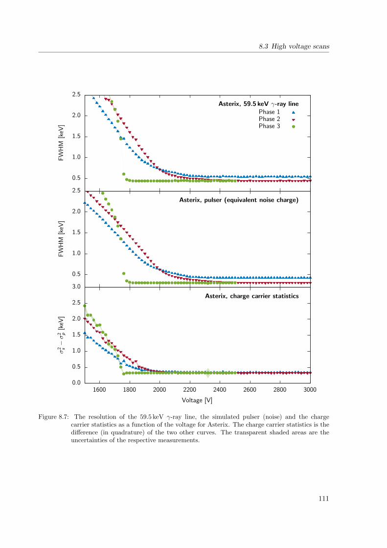
8.3 High voltage scans
0.5
1.0
1.5
2.0
2.5
FW
HM
[keV
]
Asterix, 59.5 keV γ-ray line
0.5
1.0
1.5
2.0
2.5
FW
HM
[keV
]
Asterix, pulser (equivalent noise charge)
0.0
0.5
1.0
1.5
2.0
2.5
3.0
1600 1800 2000 2200 2400 2600 2800 3000
σ2 s−σ2 p
[keV
]
Voltage [V]
Asterix, charge carrier statistics
Phase 1Phase 2Phase 3
Figure 8.7: The resolution of the 59.5 keV γ-ray line, the simulated pulser (noise) and the chargecarrier statistics as a function of the voltage for Asterix. The charge carrier statistics is thedifference (in quadrature) of the two other curves. The transparent shaded areas are theuncertainties of the respective measurements.
111
8 Results from the point contact size study
0.5
1.0
1.5
2.0
2.5
3.0
FW
HM
[keV
]
Obelix, 59.5 keV γ-ray line
0.5
1.0
1.5
2.0
2.5
3.0
FW
HM
[keV
]
Obelix, pulser (equivalent noise charge)
0.0
0.5
1.0
1.5
2.0
2.5
3.0
2000 2500 3000 3500 4000
σ2 s−σ2 p
[keV
]
Voltage [V]
Obelix, charge carrier statistics
Phase 1Phase 2
Figure 8.8: The resolution of the 59.5 keV γ-ray line, the simulated pulser (noise) and the charge carrierstatistics as a function of the voltage for Obelix. The charge carrier statistics is the difference(in quadrature) of the two other curves The transparent shaded areas are the uncertaintiesof the respective measurements.
112
8.3 High voltage scans
In the bottom panel of Fig. 8.7 and Fig. 8.8 the difference between the resolution of the59.5 keV line and the pulser (subtracted in quadrature) is plotted as a function of the depletionvoltage. This corresponds roughly to uncertainties from charge carrier statistics and is thesame as the Fano factor. Above the depletion voltage it is constant, which supports theassumption of complete charge collection made in Sec. 7.3.1. Below the depletion voltage,the value increases, which means that effects such as incomplete charge collection and pulseshape variations are the main source of uncertainties. The value classifying the charge carrierstatistics is still constant well into the region where the resolution slowly is increasing. Thisfurthermore supports a depletion voltage that lays at a voltage well below the constant region.
It is possible to explain the discrepancy between simulated depletion voltage and measure-ments with uncertainties in the description of the impurity concentration in the detector. Nextto a gradient along the height there most likely is also a radial gradient, that was not consid-ered. Furthermore, the exact values of the impurities were given with a precision of roughly10%. This leaves plenty of space for alternative impurity distributions that can explain theobserved effects.
A specific systematics that needs to be considered for high voltage scans are hysteresis effects.The detector must not behave in the same manner when the voltage is increased than whenit is decreased. In both cases, once the voltage reaches a certain level it takes a certain timefor the detector to settle and reach constant operation conditions. In order to exclude theseeffects additional measurements with 241Am and 60Co have been conducted for all detectorsconfigurations. These measurements are all consistent with what has been presented here.As previously mentioned the voltage scans have been performed from the operational voltagedownwards. In that way no temporal effects (i.e. relaxations) have been observed.
8.3.2 Relative peak position and pulse rise time
The depletion of a detector furthermore can be studied through the relative position of the re-constructed peak in the energy spectrum. Fig. 8.9 shows this dependency for the two detectors.Similar to what was observed for the resolution, the curves for the first two configurations arevery similar to each other. The final peak position is only slowly approached with increasinghigh voltage. Around 2000 V for Asterix and 2400 V for Obelix there seems to be a weak dentin the peak position, which might be related to the full depletion of the detector. Above thisvoltage the peak position still deviates by about 5% from the highest value. The same expla-nations that were given to describe the slowly increasing region in the previous section alsoapply here. Instead of the capacitance, in this case however the depletion width is relevant.The detector at high voltages is depleted further into the p+ region; charge carriers can driftcloser to the central electron before being absorbed, will reach higher values in the weightingpotential and induce a larger pulse into the electrode.
The situation is again different for Asterix at the geometry with the smallest point contactsize. There is a fast drop around the depletion voltage and below the fast drop the recon-structed position increases again for roughly 50 V. The increase can be as well explained byan undepleted bubble. Such a bubble forces the charge carriers to diffuse and thus they areeither lost or collected with a delay. This is furthermore supported by the average rise time ofevents, depicted in the bottom panels of Fig. 8.9. The charge pulse of events at this voltagetakes considerably longer to rise; the pulse shape of these events is very similar to slow eventsoriginating in the transition layer. It can be assumed that the mechanics governing their shape
113
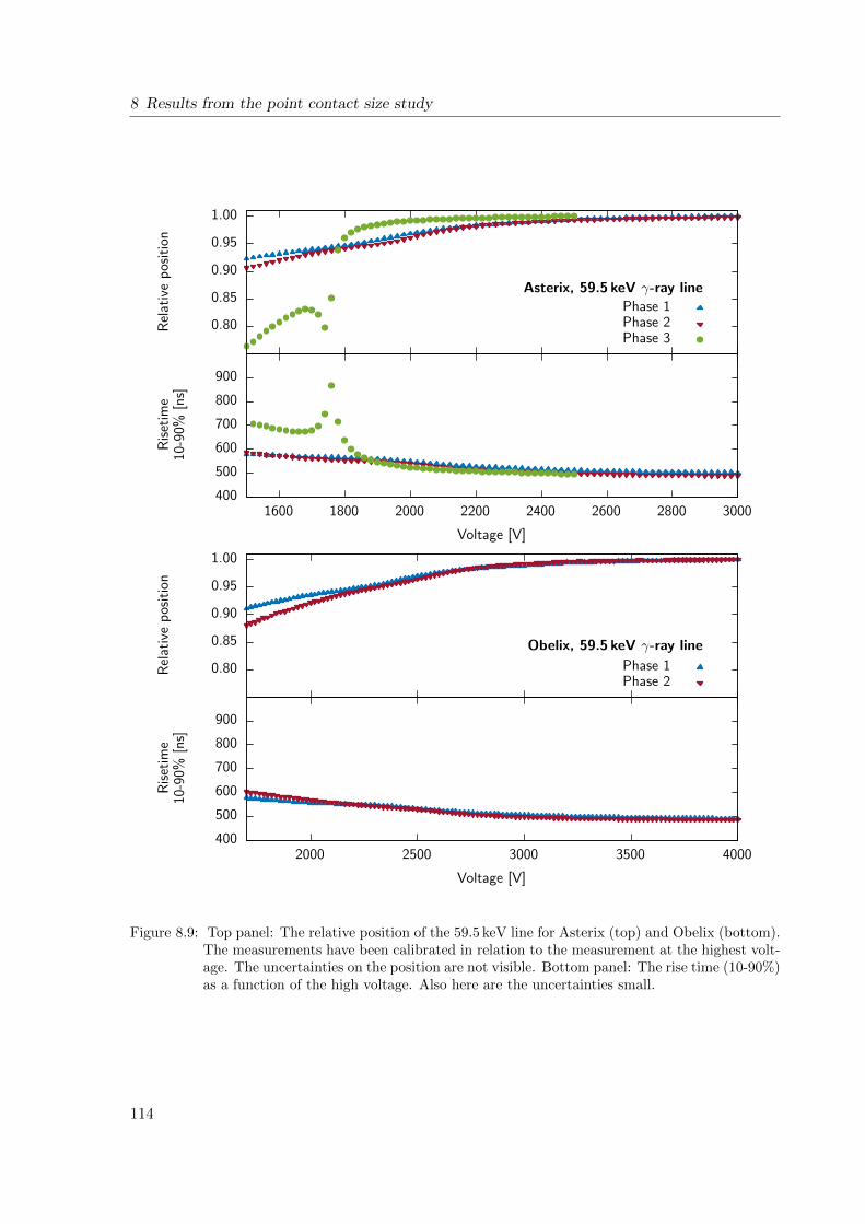
8 Results from the point contact size study
0.80
0.85
0.90
0.95
1.00
Asterix, 59.5 keV γ-ray line
Rel
ativ
ep
osit
ion
400
500
600
700
800
900
1600 1800 2000 2200 2400 2600 2800 3000
Voltage [V]
Ris
etim
e10
-90%
[ns]
Phase 1Phase 2Phase 3
0.80
0.85
0.90
0.95
1.00
Obelix, 59.5 keV γ-ray line
Rel
ativ
ep
osit
ion
400
500
600
700
800
900
2000 2500 3000 3500 4000
Voltage [V]
Ris
etim
e10
-90%
[ns]
Phase 1Phase 2
Figure 8.9: Top panel: The relative position of the 59.5 keV line for Asterix (top) and Obelix (bottom).The measurements have been calibrated in relation to the measurement at the highest volt-age. The uncertainties on the position are not visible. Bottom panel: The rise time (10-90%)as a function of the high voltage. Also here are the uncertainties small.
114
8.4 Collimated measurements near the surface
is also alike and thus should be diffusion.
The operational voltage of Asterix was fixed at 3000 V for its Phase 1 and 2 configuration and2500 V for its Phase 3 configuration; the one for Obelix at 4000 V for both configurations. Theoperational voltage, thus, is sufficiently into the plateau to exhibit a constant resolution andpeak position. However, only a few hundred of Volts below the operational voltage degradationsstarts to play a role. Effects in the range 2-5% are easily realized.
8.4 Collimated measurements near the surface
Two sets of collimated measurements have been taken at the operational voltage of the detec-tors. The first set has been taken on the scanning table with an 241Am source. The automatedprocedure allows to take measurements on a fine grid (roughly 2 mm separation between twopoints). The second set has been taken with a 133Ba source that was placed in the bore-hole ofa large Na(I) detector to track the coincidental emission of two γ-rays at energies of 81.0 keVand 356.0 keV. This measurement was performed manually and therefore restricted to a singlehorizontal line along the center of the detector (5 mm spacing). In both measurements thecollimated γ-rays interact close to the surface in a confined space. Thus, results from measure-ments can be compared to simulations from ADL3, without requiring extensive Monte Carlosimulations to establish the distribution of interactions within the detector.
The simulated pulses represent the charge that is induced into the electronic circuit not theactual pulse shape that is measured. The measured pulse is affected by the electronics chainwhich adds some shaping and noise to the signal. In theory, the effects of the electronics can bestudied by measuring the response of the system to a sharp pulser signal. Such a measurementhas been performed, however, suffers from two weakness:
• The pulser feed into the test input of the preamplifier must have a very sharp rising edgeto not affect the pulse response measurement through the finite rise time of the pulsersignal. The Hewlett Packard 8007B Pulse Generator has a rise time of roughly 5 ns,however, it seems that this still affects the impulse response of the electronics system.
• Many pulser signals will be measured, which need to be averaged, to reduce the effectof electronics noise. The averaging procedure requires some sort of alignment. Themeasured signals have been aligned by the maxima of their current pulse. However,this method also adds a bias. The results would have been more precise, if the pulsersignal were additionally feed into the FADC to establish a coincidence. Unfortunately,until recently, this method was not thought off, therefore such a measurement was notperformed.
Furthermore, a measurement also contains traces of special pulses (i.e. slow pulses) thatare explained by a simplified model and not yet implemented in ADL3. Even if it wouldbe possible to consider all these effects it is still not assured that the electrical field in thedetector can be perfectly described by the simulation. Particularly the effect of gradients inthe impurity concentration on the electric field is large, however, impurity concentrations cannot be measured completely throughout the detector.
As a discussion of all these problematics is complex and far beyond the scope of this dis-sertation only a generic comparison directly between simulated pulses and measurements will
115
8 Results from the point contact size study
be made and all the complications left aside. It will be seen, that the gain from a genericdescription is satisfactory.
8.4.1 Coincidental measurement with a NaI(Tl) detector
The radio isotope 133Ba emits two coincidental γ-particles at energies of 81.0 keV and 356.0 keV.Thus, when an event is observed in the 81.0 keV peak it should coincide with an event of356.0 keV in the NaI(Tl) detector. The energy resolution in of the NaI(Tl) detector that isused in this study is poor. However, the response is sufficient to track the onset of the signal.The position of the maxima of all peaks, that are observed simultaneously with a 81.0 keV eventare located. The time difference between the position of this signal in the NaI(Tl) detectorand the maximum of the current pulse is then filled into a histogram. The observed spectrumis flat except for the location where the coincidental γ-ray is detected and where a sharp peakis observe. This peak provides a rough estimation for the position-dependent drift time of thecharge carriers in the germanium detector.
The results are plotted in the right panel of Fig. 8.10 at different radii. As expected, withincreasing radii also the drift time increases. On the left panel of Fig. 8.10 the same effectis represented from simulation. It can be seen that the shape of the curve matches the data.Also the relative differences between the different point contact sizes is well explained by thesimulation. The absolute values of the simulations and the measurements do not match: Forsimulations the onset of the pulse can be defined relative precisely, for the measured data thelocation of the maximum of the NaI(Tl) signal was used. The response time of the NaI(Tl)detector is about 100 ns, which corresponds roughly to the observed difference between dataand measurement.
The coincidence measured in the NaI(Tl) detector can be used to correctly align the signalsin the germanium detector. This procedure was used to find the average pulse shape of signalsfrom a given radius represented in Fig. 8.11. The difference between the simulated signal andthe measured signal comes from electronics components, which shapes the signal obtained fromthe germanium detector and thus brings it into the measured form. Except of these differencesthe signals seem to match the simulation well, particularly the drift time of the average pulseroughly matches what the simulation predicts. However, signals that originate close to thecenter of the diode rise slightly faster in the data while signals at a large radius rise slightlyslower than simulated.
8.4.2 Relative position
Measurements with a collimated 241Am source at various radius can be used to investigateregions with charge trapping within the detector. In these measurements, energy is depositedclose to the surface in a very restricted area of the detector. The charge carriers then driftthrough the entire detection volume, to be collected at the point contact. If they encounter aregion with increased charge trapping then some of the charge carriers will not contribute to thesignal that is induced into the electrode and the pulse height and shape altered. Even, if chargetrapping is homogeneous throughout the detector, it should be visible in this measurement, asthe length of the charge carrier’s trajectory depends on the initial position. With long tracksthe chance for a charge carriers to be trapped increases, thus trapping effect must be strongerat large radii from the center of the detector.
116
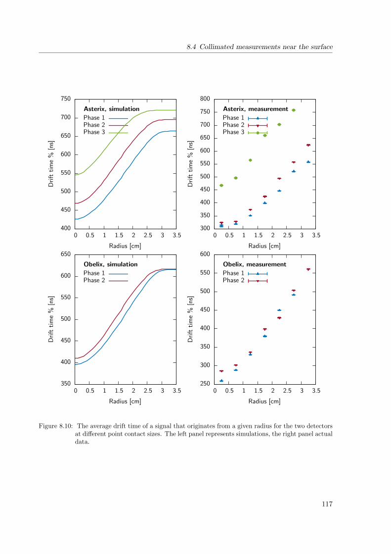
8.4 Collimated measurements near the surface
400
450
500
550
600
650
700
750
0 0.5 1 1.5 2 2.5 3 3.5
Dri
ftti
me
%[n
s]
Radius [cm]
Asterix, simulation
Phase 1Phase 2Phase 3
300
350
400
450
500
550
600
650
700
750
800
0 0.5 1 1.5 2 2.5 3 3.5
Dri
ftti
me
%[n
s]
Radius [cm]
Asterix, measurement
Phase 1Phase 2Phase 3
350
400
450
500
550
600
650
0 0.5 1 1.5 2 2.5 3 3.5
Dri
ftti
me
%[n
s]
Radius [cm]
Obelix, simulation
Phase 1Phase 2
250
300
350
400
450
500
550
600
0 0.5 1 1.5 2 2.5 3 3.5
Dri
ftti
me
%[n
s]
Radius [cm]
Obelix, measurement
Phase 1Phase 2
Figure 8.10: The average drift time of a signal that originates from a given radius for the two detectorsat different point contact sizes. The left panel represents simulations, the right panel actualdata.
117
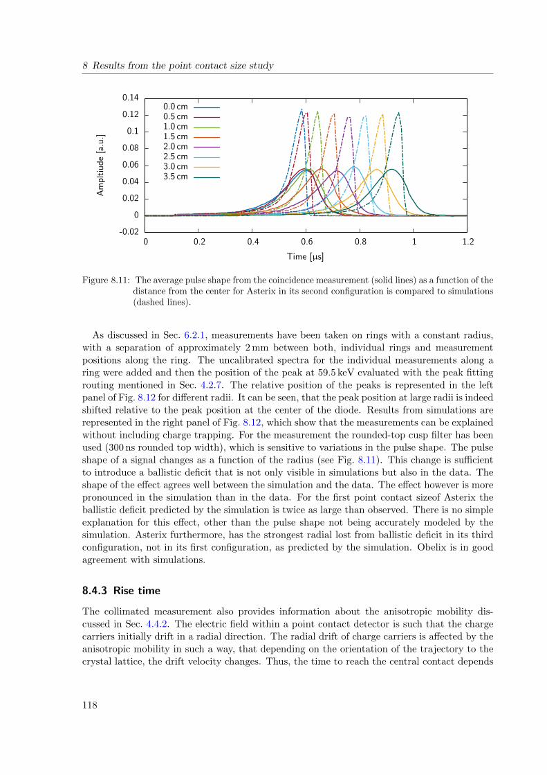
8 Results from the point contact size study
-0.02
0
0.02
0.04
0.06
0.08
0.1
0.12
0.14
0 0.2 0.4 0.6 0.8 1 1.2
Am
plt
iud
e[a
.u.]
Time [µs]
0.0 cm0.5 cm1.0 cm1.5 cm2.0 cm2.5 cm3.0 cm3.5 cm
Figure 8.11: The average pulse shape from the coincidence measurement (solid lines) as a function of thedistance from the center for Asterix in its second configuration is compared to simulations(dashed lines).
As discussed in Sec. 6.2.1, measurements have been taken on rings with a constant radius,with a separation of approximately 2 mm between both, individual rings and measurementpositions along the ring. The uncalibrated spectra for the individual measurements along aring were added and then the position of the peak at 59.5 keV evaluated with the peak fittingrouting mentioned in Sec. 4.2.7. The relative position of the peaks is represented in the leftpanel of Fig. 8.12 for different radii. It can be seen, that the peak position at large radii is indeedshifted relative to the peak position at the center of the diode. Results from simulations arerepresented in the right panel of Fig. 8.12, which show that the measurements can be explainedwithout including charge trapping. For the measurement the rounded-top cusp filter has beenused (300 ns rounded top width), which is sensitive to variations in the pulse shape. The pulseshape of a signal changes as a function of the radius (see Fig. 8.11). This change is sufficientto introduce a ballistic deficit that is not only visible in simulations but also in the data. Theshape of the effect agrees well between the simulation and the data. The effect however is morepronounced in the simulation than in the data. For the first point contact sizeof Asterix theballistic deficit predicted by the simulation is twice as large than observed. There is no simpleexplanation for this effect, other than the pulse shape not being accurately modeled by thesimulation. Asterix furthermore, has the strongest radial lost from ballistic deficit in its thirdconfiguration, not in its first configuration, as predicted by the simulation. Obelix is in goodagreement with simulations.
8.4.3 Rise time
The collimated measurement also provides information about the anisotropic mobility dis-cussed in Sec. 4.4.2. The electric field within a point contact detector is such that the chargecarriers initially drift in a radial direction. The radial drift of charge carriers is affected by theanisotropic mobility in such a way, that depending on the orientation of the trajectory to thecrystal lattice, the drift velocity changes. Thus, the time to reach the central contact depends
118
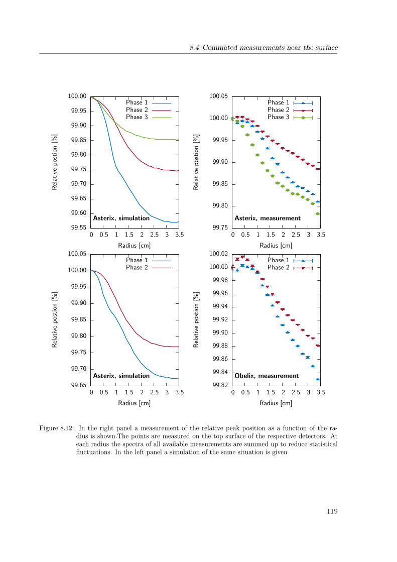
8.4 Collimated measurements near the surface
99.55
99.60
99.65
99.70
99.75
99.80
99.85
99.90
99.95
100.00
0 0.5 1 1.5 2 2.5 3 3.5
Rel
ativ
ep
osti
on[%
]
Radius [cm]
Asterix, simulation
Phase 1Phase 2Phase 3
99.75
99.80
99.85
99.90
99.95
100.00
100.05
0 0.5 1 1.5 2 2.5 3 3.5
Rel
ativ
ep
osti
on[%
]
Radius [cm]
Asterix, measurement
Phase 1Phase 2Phase 3
99.65
99.70
99.75
99.80
99.85
99.90
99.95
100.00
100.05
0 0.5 1 1.5 2 2.5 3 3.5
Rel
ativ
ep
osti
on[%
]
Radius [cm]
Asterix, simulation
Phase 1Phase 2
99.82
99.84
99.86
99.88
99.90
99.92
99.94
99.96
99.98
100.00
100.02
0 0.5 1 1.5 2 2.5 3 3.5
Rel
ativ
ep
osti
on[%
]
Radius [cm]
Obelix, measurement
Phase 1Phase 2
Figure 8.12: In the right panel a measurement of the relative peak position as a function of the ra-dius is shown.The points are measured on the top surface of the respective detectors. Ateach radius the spectra of all available measurements are summed up to reduce statisticalfluctuations. In the left panel a simulation of the same situation is given
119
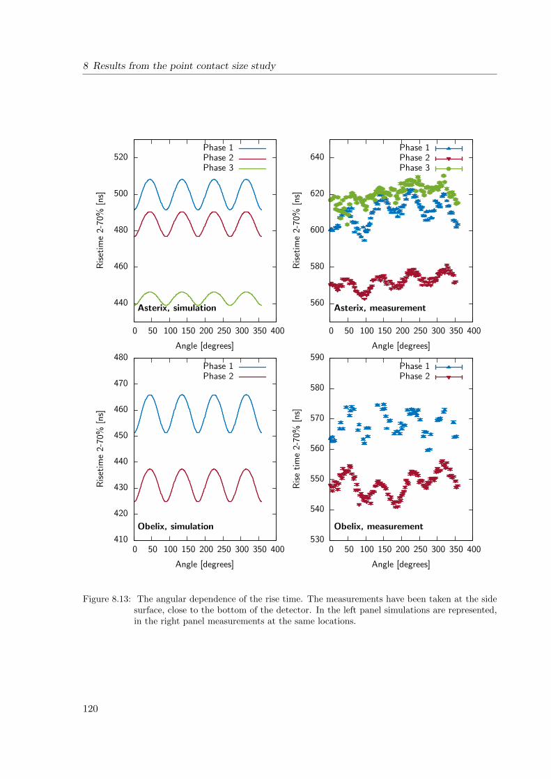
8 Results from the point contact size study
440
460
480
500
520
0 50 100 150 200 250 300 350 400
Ris
etim
e2-
70%
[ns]
Angle [degrees]
Phase 1Phase 2Phase 3
Asterix, simulation560
580
600
620
640
0 50 100 150 200 250 300 350 400
Ris
etim
e2-
70%
[ns]
Angle [degrees]
Phase 1Phase 2Phase 3
Asterix, measurement
410
420
430
440
450
460
470
480
0 50 100 150 200 250 300 350 400
Ris
etim
e2-
70%
[ns]
Angle [degrees]
Phase 1Phase 2
Obelix, simulation
530
540
550
560
570
580
590
0 50 100 150 200 250 300 350 400
Ris
eti
me
2-70
%[n
s]
Angle [degrees]
Phase 1Phase 2
Obelix, measurement
Figure 8.13: The angular dependence of the rise time. The measurements have been taken at the sidesurface, close to the bottom of the detector. In the left panel simulations are represented,in the right panel measurements at the same locations.
120
8.4 Collimated measurements near the surface
on the angle at which the charge is deposited relative to the crystal lattice. Particularly, theonset of the signal is sensitive to this effect, thus the rise time 2-70% is used to measure theanisotropic mobility. When the rise time from 2-70% is plotted against the angle, characteristicoscillations appear as represented in Fig. 8.13. The oscillations can be observed in any of thedifferent configurations, however, for Asterix in its third configuration they are relatively weak.The oscillations are predicted by ADL3, as the anisotropic mobility is included in the simula-tion. However, the figure also shows that the absolute values of the rise time do not agree wellbetween simulation and measurements. Especially, the third configuration of Asterix does notfollow what was predicted by the simulation: It is in average not found at a lower rise timethan the other two configurations, instead it is shifted to a higher value, similar to its Phase 1configuration.
8.4.4 Effects observed with collimated measurements
In the previous sections it was shown that there is quantitative agreement between simulationsand measurements, when it comes to the radial and angular variations between different pointsalong the surface. However, it was also discovered that absolute measurement values do notmatch the predictions well. Particularly the third configuration of Asterix seems not to behaveaccording to the simulation, while the first and second configuration of Asterix and Obelixfollow the overall predictions. This agrees with the results from the high voltage scans (seeSec. 8.3), where also the third configuration of Asterix is different from the larger point contactsizes.
These discrepancies can not be easily explained as they do not show up in the simulations.The operational voltage of Asterix in its third configuration was lowered to 2500 V as leakagecurrents were increased. The lower operational voltage, however, can not explain the observedeffects then the reduced depletion voltage was considered in the simulation.
The effect could be caused by an insufficiently precise knowledge of the impurity concentra-tions. It is possible, that the impurity gradient not only varies along the height of the diodebut also in the radial direction. Furthermore, with roughly 10% precision (measured by Can-berra), also the variation along the height could be different from the value considered in thesimulation. Differences in the impurity gradient might explain both observation, an increaseddepletion voltage compared to simulations in the first two configurations and differences in theshape of the signal in the third configuration.
Except the odd behavior of Asterix, it has been shown, that effects that are predicted bysimulations show up in the data. Even though the data and measurements do not matchperfectly, most of the differences can be contributed to the effects described in the beginningof this section, especially that the electronics response function was not considered. Thequalitative agreement, is sufficient to understand the physics behind the signal formation andexplain why certain effects arise. A complete description of the system including all the effectsthat were left out in this discussion would not add a lot of new information. The overalldiscrepancies most likely can not be resolved in such a manner, but rather hint some systematicsin the simulation. Therefore, the approach to neglect these details and mainly search for aqualitative understanding of the processes is justified.
121
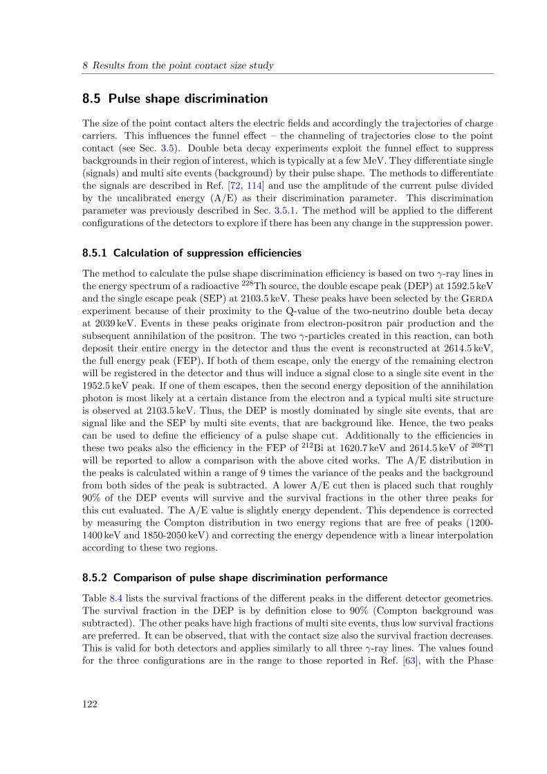
8 Results from the point contact size study
8.5 Pulse shape discrimination
The size of the point contact alters the electric fields and accordingly the trajectories of chargecarriers. This influences the funnel effect – the channeling of trajectories close to the pointcontact (see Sec. 3.5). Double beta decay experiments exploit the funnel effect to suppressbackgrounds in their region of interest, which is typically at a few MeV. They differentiate single(signals) and multi site events (background) by their pulse shape. The methods to differentiatethe signals are described in Ref. [72, 114] and use the amplitude of the current pulse dividedby the uncalibrated energy (A/E) as their discrimination parameter. This discriminationparameter was previously described in Sec. 3.5.1. The method will be applied to the differentconfigurations of the detectors to explore if there has been any change in the suppression power.
8.5.1 Calculation of suppression efficiencies
The method to calculate the pulse shape discrimination efficiency is based on two γ-ray lines inthe energy spectrum of a radioactive 228Th source, the double escape peak (DEP) at 1592.5 keVand the single escape peak (SEP) at 2103.5 keV. These peaks have been selected by the Gerdaexperiment because of their proximity to the Q-value of the two-neutrino double beta decayat 2039 keV. Events in these peaks originate from electron-positron pair production and thesubsequent annihilation of the positron. The two γ-particles created in this reaction, can bothdeposit their entire energy in the detector and thus the event is reconstructed at 2614.5 keV,the full energy peak (FEP). If both of them escape, only the energy of the remaining electronwill be registered in the detector and thus will induce a signal close to a single site event in the1952.5 keV peak. If one of them escapes, then the second energy deposition of the annihilationphoton is most likely at a certain distance from the electron and a typical multi site structureis observed at 2103.5 keV. Thus, the DEP is mostly dominated by single site events, that aresignal like and the SEP by multi site events, that are background like. Hence, the two peakscan be used to define the efficiency of a pulse shape cut. Additionally to the efficiencies inthese two peaks also the efficiency in the FEP of 212Bi at 1620.7 keV and 2614.5 keV of 208Tlwill be reported to allow a comparison with the above cited works. The A/E distribution inthe peaks is calculated within a range of 9 times the variance of the peaks and the backgroundfrom both sides of the peak is subtracted. A lower A/E cut then is placed such that roughly90% of the DEP events will survive and the survival fractions in the other three peaks forthis cut evaluated. The A/E value is slightly energy dependent. This dependence is correctedby measuring the Compton distribution in two energy regions that are free of peaks (1200-1400 keV and 1850-2050 keV) and correcting the energy dependence with a linear interpolationaccording to these two regions.
8.5.2 Comparison of pulse shape discrimination performance
Table 8.4 lists the survival fractions of the different peaks in the different detector geometries.The survival fraction in the DEP is by definition close to 90% (Compton background wassubtracted). The other peaks have high fractions of multi site events, thus low survival fractionsare preferred. It can be observed, that with the contact size also the survival fraction decreases.This is valid for both detectors and applies similarly to all three γ-ray lines. The values foundfor the three configurations are in the range to those reported in Ref. [63], with the Phase
122
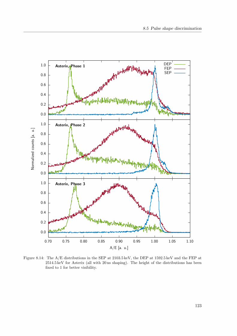
8.5 Pulse shape discrimination
0.0
0.2
0.4
0.6
0.8
1.0
0.0
0.2
0.4
0.6
0.8
1.0
0.0
0.2
0.4
0.6
0.8
1.0
0.70 0.75 0.80 0.85 0.90 0.95 1.00 1.05 1.10
A/E [a. u.]
Nor
mal
ized
cou
nts
[a.
u.]
DEPFEPSEP
Asterix, Phase 1
Asterix, Phase 2
Asterix, Phase 3
Figure 8.14: The A/E distributions in the SEP at 2103.5 keV, the DEP at 1592.5 keV and the FEP at2514.5 keV for Asterix (all with 20 ns shaping). The height of the distributions has beenfixed to 1 for better visibility.
123
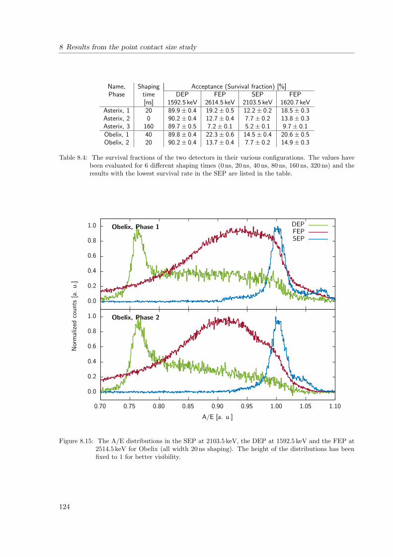
8 Results from the point contact size study
Name, Shaping Acceptance (Survival fraction) [%]Phase time DEP FEP SEP FEP
[ns] 1592.5 keV 2614.5 keV 2103.5 keV 1620.7 keVAsterix, 1 20 89.9± 0.4 19.2± 0.5 12.2± 0.2 18.5± 0.3Asterix, 2 0 90.2± 0.4 12.7± 0.4 7.7± 0.2 13.8± 0.3Asterix, 3 160 89.7± 0.5 7.2± 0.1 5.2± 0.1 9.7± 0.1Obelix, 1 40 89.8± 0.4 22.3± 0.6 14.5± 0.4 20.6± 0.5Obelix, 2 20 90.2± 0.4 13.7± 0.4 7.7± 0.2 14.9± 0.3
Table 8.4: The survival fractions of the two detectors in their various configurations. The values havebeen evaluated for 6 different shaping times (0 ns, 20 ns, 40 ns, 80 ns, 160 ns, 320 ns) and theresults with the lowest survival rate in the SEP are listed in the table.
0.0
0.2
0.4
0.6
0.8
1.0
Nor
mal
ized
cou
nts
[a.
u.]
0.0
0.2
0.4
0.6
0.8
1.0
0.70 0.75 0.80 0.85 0.90 0.95 1.00 1.05 1.10
A/E [a. u.]
DEPFEPSEP
Obelix, Phase 1
Obelix, Phase 2
Figure 8.15: The A/E distributions in the SEP at 2103.5 keV, the DEP at 1592.5 keV and the FEP at2514.5 keV for Obelix (all width 20 ns shaping). The height of the distributions has beenfixed to 1 for better visibility.
124
8.5 Pulse shape discrimination
1 configuration of Asterix and Obelix being on the high side and their respective Phase 2configuration around the average of the reported values. The Phase 3 value of Asterix is ingood agreement with the best values found in that reference.
The A/E distributions of Asterix in its three configurations are shown in Fig. 8.14 for theSEP, DEP and FEP (2614.5 keV). On the left shoulder of the DEP there is a secondary structurevisible that disappears once the point contact is reduced. This non-Gaussian structure of theDEP has been also observed in Ref. [63] for some detectors. Furthermore, the SEP and theFEP distribution are shifted to the left as the point contact size is reduced which is the originof the improve discrimination efficiency. The same observations are also valid for the twoconfigurations of Obelix shown in Fig. 8.15.
The reduction of the point contact size increases the funnel effect by confining the weightingfield to an even closer region around the point contact. The improvement is therefore expected,however, has not yet conclusively been proven. The successive improvement of the pulse shapediscrimination efficiencies with a reduction of the point contact size observed in this workis a strong evidence, that a small point contact is indeed beneficial for a good pulse shapediscrimination performance of a detector. The suppression power is limited as inevitably thereare some single site event-like signals in both the FEPs and the SEP. However, the presentedstudy proves, that there is still some space for improvements compared to the detector geometryof Ref. [63]. Detectors produced according to the geometry studied in this dissertation mightbe highly interesting for a further detector production of this or other neutrinoless double betadecay experiments.
125
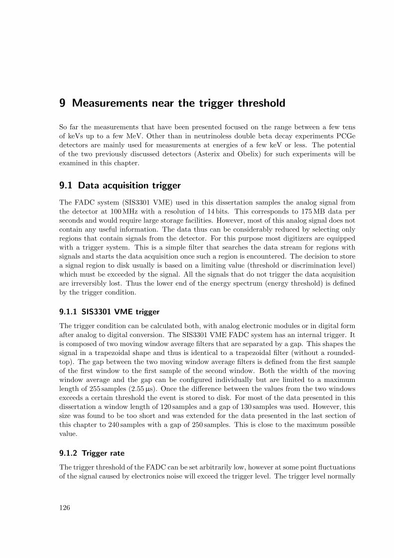
9 Measurements near the trigger threshold
So far the measurements that have been presented focused on the range between a few tensof keVs up to a few MeV. Other than in neutrinoless double beta decay experiments PCGedetectors are mainly used for measurements at energies of a few keV or less. The potentialof the two previously discussed detectors (Asterix and Obelix) for such experiments will beexamined in this chapter.
9.1 Data acquisition trigger
The FADC system (SIS3301 VME) used in this dissertation samples the analog signal fromthe detector at 100 MHz with a resolution of 14 bits. This corresponds to 175 MB data perseconds and would require large storage facilities. However, most of this analog signal does notcontain any useful information. The data thus can be considerably reduced by selecting onlyregions that contain signals from the detector. For this purpose most digitizers are equippedwith a trigger system. This is a simple filter that searches the data stream for regions withsignals and starts the data acquisition once such a region is encountered. The decision to storea signal region to disk usually is based on a limiting value (threshold or discrimination level)which must be exceeded by the signal. All the signals that do not trigger the data acquisitionare irreversibly lost. Thus the lower end of the energy spectrum (energy threshold) is definedby the trigger condition.
9.1.1 SIS3301 VME trigger
The trigger condition can be calculated both, with analog electronic modules or in digital formafter analog to digital conversion. The SIS3301 VME FADC system has an internal trigger. Itis composed of two moving window average filters that are separated by a gap. This shapes thesignal in a trapezoidal shape and thus is identical to a trapezoidal filter (without a rounded-top). The gap between the two moving window average filters is defined from the first sampleof the first window to the first sample of the second window. Both the width of the movingwindow average and the gap can be configured individually but are limited to a maximumlength of 255 samples (2.55µs). Once the difference between the values from the two windowsexceeds a certain threshold the event is stored to disk. For most of the data presented in thisdissertation a window length of 120 samples and a gap of 130 samples was used. However, thissize was found to be too short and was extended for the data presented in the last section ofthis chapter to 240 samples with a gap of 250 samples. This is close to the maximum possiblevalue.
9.1.2 Trigger rate
The trigger threshold of the FADC can be set arbitrarily low, however at some point fluctuationsof the signal caused by electronics noise will exceed the trigger level. The trigger level normally
126
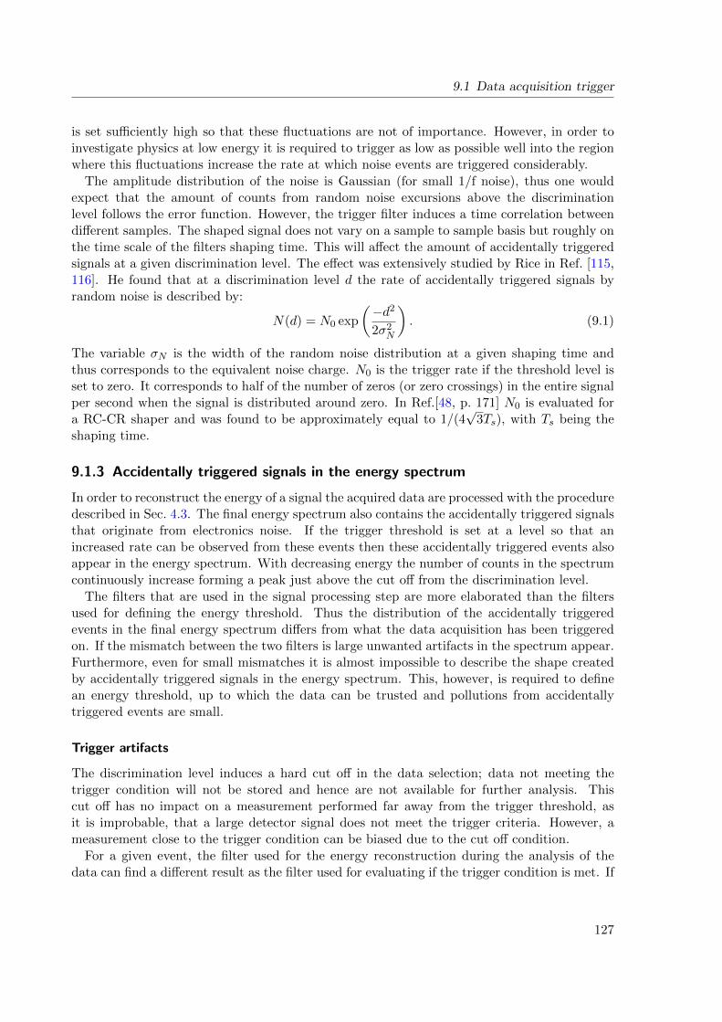
9.1 Data acquisition trigger
is set sufficiently high so that these fluctuations are not of importance. However, in order toinvestigate physics at low energy it is required to trigger as low as possible well into the regionwhere this fluctuations increase the rate at which noise events are triggered considerably.
The amplitude distribution of the noise is Gaussian (for small 1/f noise), thus one wouldexpect that the amount of counts from random noise excursions above the discriminationlevel follows the error function. However, the trigger filter induces a time correlation betweendifferent samples. The shaped signal does not vary on a sample to sample basis but roughly onthe time scale of the filters shaping time. This will affect the amount of accidentally triggeredsignals at a given discrimination level. The effect was extensively studied by Rice in Ref. [115,116]. He found that at a discrimination level d the rate of accidentally triggered signals byrandom noise is described by:
N(d) = N0 exp
(−d2
2σ2N
). (9.1)
The variable σN is the width of the random noise distribution at a given shaping time andthus corresponds to the equivalent noise charge. N0 is the trigger rate if the threshold level isset to zero. It corresponds to half of the number of zeros (or zero crossings) in the entire signalper second when the signal is distributed around zero. In Ref.[48, p. 171] N0 is evaluated fora RC-CR shaper and was found to be approximately equal to 1/(4
√3Ts), with Ts being the
shaping time.
9.1.3 Accidentally triggered signals in the energy spectrum
In order to reconstruct the energy of a signal the acquired data are processed with the proceduredescribed in Sec. 4.3. The final energy spectrum also contains the accidentally triggered signalsthat originate from electronics noise. If the trigger threshold is set at a level so that anincreased rate can be observed from these events then these accidentally triggered events alsoappear in the energy spectrum. With decreasing energy the number of counts in the spectrumcontinuously increase forming a peak just above the cut off from the discrimination level.
The filters that are used in the signal processing step are more elaborated than the filtersused for defining the energy threshold. Thus the distribution of the accidentally triggeredevents in the final energy spectrum differs from what the data acquisition has been triggeredon. If the mismatch between the two filters is large unwanted artifacts in the spectrum appear.Furthermore, even for small mismatches it is almost impossible to describe the shape createdby accidentally triggered signals in the energy spectrum. This, however, is required to definean energy threshold, up to which the data can be trusted and pollutions from accidentallytriggered events are small.
Trigger artifacts
The discrimination level induces a hard cut off in the data selection; data not meeting thetrigger condition will not be stored and hence are not available for further analysis. Thiscut off has no impact on a measurement performed far away from the trigger threshold, asit is improbable, that a large detector signal does not meet the trigger criteria. However, ameasurement close to the trigger condition can be biased due to the cut off condition.
For a given event, the filter used for the energy reconstruction during the analysis of thedata can find a different result as the filter used for evaluating if the trigger condition is met. If
127
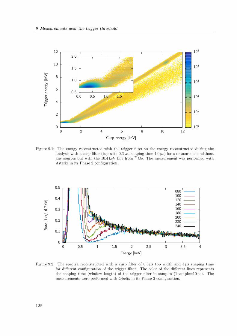
9 Measurements near the trigger threshold
Tri
gger
ener
gy[k
eV]
Cusp energy [keV]
0
2
4
6
8
10
12
0 2 4 6 8 10 12100
101
102
103
104
105
0.5
1.0
1.5
2.0
0.0 0.5 1.0 1.5
Figure 9.1: The energy reconstructed with the trigger filter vs the energy reconstructed during theanalysis with a cusp filter (top with 0.3µs, shaping time 4.0µs) for a measurement withoutany sources but with the 10.4 keV line from 71Ge. The measurement was performed withAsterix in its Phase 2 configuration.
0
0.1
0.2
0.3
0.4
0.5
0 0.5 1 1.5 2 2.5 3 3.5 4
Rat
e[1
/s/1
6.7
eV]
Energy [keV]
080100120140160180200220240
Figure 9.2: The spectra reconstructed with a cusp filter of 0.3µs top width and 4µs shaping timefor different configuration of the trigger filter. The color of the different lines representsthe shaping time (window length) of the trigger filter in samples (1 sample=10 ns). Themeasurements were performed with Obelix in its Phase 2 configuration.
128

9.1 Data acquisition trigger
the energy reconstructed during the analysis is lower than the one reconstructed by the triggerthe event is reconstructed below the trigger cut off and instead of observing a straight cut off,the drop to zero spreads over a certain range. However, if the trigger condition reconstructsan event below the threshold but the shaping filter would have reconstructed the event abovethe trigger threshold then data are wrongly rejected and missing from the energy spectrum.
This effect was observed for measurements near the energy threshold and its effect causedspectral distortions up to an energy of a few keV. The effect is represented in Fig. 9.1, wherethe energy determined by the data analysis filter is plotted against the energy found by thetrigger filter. The measurement has been taken after irradiation of the detector with the 252Cfsource leading to a peak at 10.4 keV from deexcitations of the isomer 71mGe. The cut off by thetrigger is represented as a vertical line in the spectrum, below which no events can be found.The small deviation from a straight cut are caused by small differences in the algorithm usedfor reconstructing the trigger filter value in software and the actual algorithm implementedin the FADCs (the details of the algorithm were not accessible and could only be reproducedwith limited precision). The energy of many events in that figure are reconstructed by thetwo filters at different energies. The upper band that contains the peak at 10.4 keV consists ofevents that were reconstructed with a similar energy in both filters. The lower band consistsof events that were reconstructed at a much lower energy with the trigger filter. These eventsare mostly slow pulses that originate from external γ-rays depositing energy in the transitionlayer (see Section 3.4). The rise time of slow pulses is often large (> 1.5µs). These events thuscan not be reconstructed correctly with a filter of only 1.2µs width. The value for the energy isaccordingly underestimated. The cusp filter that was used during the signal processing on thecontrary has a sufficiently large shaping time to reconstruct the energy correctly. The lowerband with the slow pulses extends all the way down to the trigger threshold and is cut off bythe threshold between 0.8 and 1.5 keV.
Figure 9.2 shows the spectrum that was reconstructed with a cusp filter of 4µs shaping timefor a variety of measurements taken with different trigger filter settings. It can be seen, thatthe smaller the shaping type of the trigger filter the more pronounced is the appearance ofa fake peak in the region between 0.8 and 1.8 keV. If the shaping time of the trigger filter ischosen to be close to the maximum value (2.4µs), the trigger filter is capable of reconstructionalso the energy of slow pulses and the fake peak disappears.
In order to avoid these effects near the threshold it is thus important to already implementa sufficiently powerful filter for data triggering. For an analysis with a PCGe detector thetrigger implemented in the VME FADC module might be sufficient when choosing the longestavailable window length. In experiments that try to perform physics measurements close tothe threshold it is however beneficial to use an external trigger instead of the one implementedin the FADCs to avoid this bias at all cost.
Distribution of accidentally triggered signals
The analysis of the detailed distribution of the noise spectrum above a certain discriminationlevel is extremely complex on a theoretical level, and beyond the scope of this thesis. Thediscussion here is thus limited to some simple considerations that are used later on for fittingthe spectrum of accidentally triggered events.
The simplest description of the energy distribution of accidental triggered events can bederived from the amplitude distribution of random noise, which is Gaussian. If each individual
129
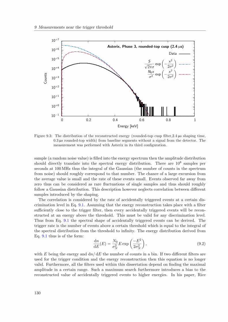
9 Measurements near the trigger threshold
10−1
10+0
10+1
10+2
10+3
10+4
10+5
10+6
10+7
0 0.2 0.4 0.6 0.8 1
Cou
nts
Energy [keV]
Data
S√2πσ
exp
(− x2
2σ2
)N0x
σ2exp
(− x2
2σ2
)
Asterix, Phase 3, rounded-top cusp (2.4µs)
Figure 9.3: The distribution of the reconstructed energy (rounded-top cusp filter,2.4µs shaping time,0.3µs rounded-top width) from baseline segments without a signal from the detector. Themeasurement was performed with Asterix in its third configuration.
sample (a random noise value) is filled into the energy spectrum then the amplitude distributionshould directly translate into the spectral energy distribution. There are 108 samples perseconds at 100 MHz thus the integral of the Gaussian (the number of counts in the spectrumfrom noise) should roughly correspond to that number. The chance of a large excursion fromthe average value is small and the rate of these events small. Events observed far away fromzero thus can be considered as rare fluctuations of single samples and thus should roughlyfollow a Gaussian distribution. This description however neglects correlation between differentsamples introduced by the shaping.
The correlation is considered by the rate of accidentally triggered events at a certain dis-crimination level in Eq. 9.1. Assuming that the energy reconstruction takes place with a filtersufficiently close to the trigger filter, then every accidentally triggered events will be recon-structed at an energy above the threshold. This must be valid for any discrimination level.Thus from Eq. 9.1 the spectral shape of accidentally triggered events can be derived. Thetrigger rate is the number of events above a certain threshold which is equal to the integral ofthe spectral distribution from the threshold to infinity. The energy distribution derived fromEq. 9.1 thus is of the form:
dn
dE(E) =
N0
σ2N
E exp
(−E2
2σ2N
), (9.2)
with E being the energy and dn/ dE the number of counts in a bin. If two different filters areused for the trigger condition and the energy reconstruction then this equation is no longervalid. Furthermore, all the filters used within this dissertation depend on finding the maximalamplitude in a certain range. Such a maximum search furthermore introduces a bias to thereconstructed value of accidentally triggered events to higher energies. In his paper, Rice
130
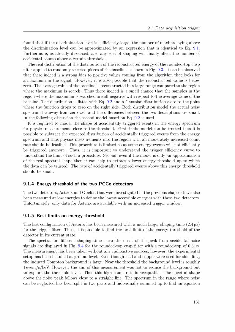
9.1 Data acquisition trigger
found that if the discrimination level is sufficiently large, the number of maxima laying abovethe discrimination level can be approximated by an expression that is identical to Eq. 9.1.Furthermore, as already discussed, also any sort of shaping will finally affect the number ofaccidental counts above a certain threshold.
The real distribution of the distribution of the reconstructed energy of the rounded-top cuspfilter applied to randomly selected pieces of the baseline is shown in Fig. 9.3. It can be observedthat there indeed is a strong bias to positive values coming from the algorithm that looks fora maximum in the signal. However, it is also possible that the reconstructed value is belowzero. The average value of the baseline is reconstructed in a large range compared to the regionwhere the maximum is search. Thus there indeed is a small chance that the samples in theregion where the maximum is searched are all negative with respect to the average value of thebaseline. The distribution is fitted with Eq. 9.2 and a Gaussian distribution close to the pointwhere the function drops to zero on the right side. Both distribution model the actual noisespectrum far away from zero well and the differences between the two descriptions are small.In the following discussion the second model based on Eq. 9.2 is used.
It is required to model the shape of accidentally triggered events in the energy spectrumfor physics measurements close to the threshold. First, if the model can be trusted then it ispossible to subtract the expected distribution of accidentally triggered events from the energyspectrum and thus physics measurements into the region with an moderately increased countrate should be feasible. This procedure is limited as at some energy events will not efficientlybe triggered anymore. Thus, it is important to understand the trigger efficiency curve tounderstand the limit of such a procedure. Second, even if the model is only an approximationof the real spectral shape then it can help to extract a lower energy threshold up to whichthe data can be trusted. The rate of accidentally triggered events above this energy thresholdshould be small.
9.1.4 Energy threshold of the two PCGe detectors
The two detectors, Asterix and Obelix, that were investigated in the previous chapter have alsobeen measured at low energies to define the lowest accessible energies with these two detectors.Unfortunately, only data for Asterix are available with an increased trigger window.
9.1.5 Best limits on energy threshold
The last configuration of Asterix has been measured with a much larger shaping time (2.4µs)for the trigger filter. Thus, it is possible to find the best limit of the energy threshold of thedetector in its current state.
The spectra for different shaping times near the onset of the peak from accidental noisesignals are displayed in Fig. 9.4 for the rounded-top cusp filter with a rounded-top of 0.3µs.The measurement has been taken without any radioactive sources, however, the experimentalsetup has been installed at ground level. Even though lead and copper were used for shielding,the induced Compton background is large. Near the threshold the background level is roughly1 event/s/keV. However, the aim of this measurement was not to reduce the background butto explore the threshold level. Thus this high count rate is acceptable. The spectral shapeabove the noise peak follows close to a straight line. The spectrum in the range where noisecan be neglected has been split in two parts and individually summed up to find an equation
131
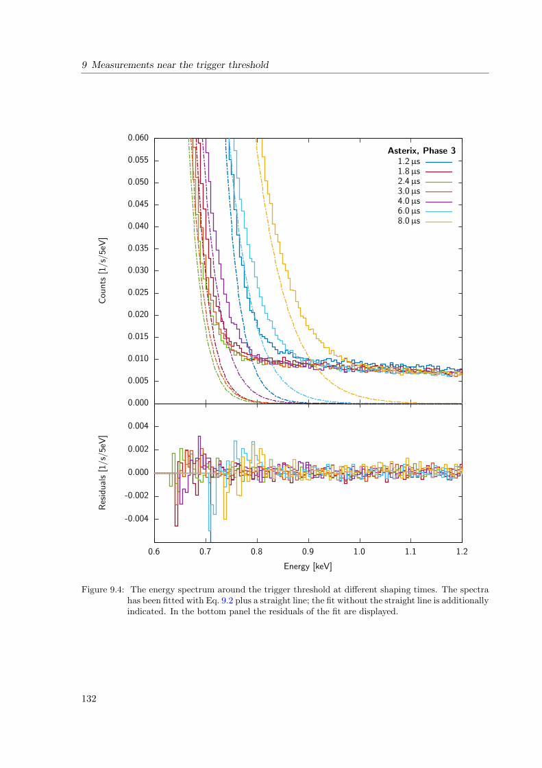
9 Measurements near the trigger threshold
0.000
0.005
0.010
0.015
0.020
0.025
0.030
0.035
0.040
0.045
0.050
0.055
0.060
Cou
nts
[1/s
/5eV
]
-0.004
-0.002
0.000
0.002
0.004
0.6 0.7 0.8 0.9 1.0 1.1 1.2
Energy [keV]
Res
idu
als
[1/s
/5eV
]
1.2µs1.8µs2.4µs3.0µs4.0µs6.0µs8.0µs
Asterix, Phase 3
Figure 9.4: The energy spectrum around the trigger threshold at different shaping times. The spectrahas been fitted with Eq. 9.2 plus a straight line; the fit without the straight line is additionallyindicated. In the bottom panel the residuals of the fit are displayed.
132
9.1 Data acquisition trigger
0.3
0.3
0.4
0.4
0.5
0.5
Res
olu
tion
[keV
]
0.5
0.6
0.7
0.8
0.9
1.0
1.1
1.2
1.0 2.0 3.0 4.0 5.0 6.0 7.0 8.0
Shaping time [µs]
En
ergy
thre
shol
d[k
eV]
fit to thresholdpulser simulation
Asterix, Phase 3
10+0 counts/s10−1 counts/s10−2 counts/s
Figure 9.5: In the top panel the variance found by fitting Eq. 9.2 to the spectrum of accidentally trig-gered noise signals is shown together with the noise resolution found with the pulser simu-lation method and already displayed in Fig. 8.4. In the bottom panel the energy thresholdis shown for three accepted accidental noise count rates. The data are from a measurementwith Asterix.
133
9 Measurements near the trigger threshold
for the straight line segment. This equation has been subtracted from the spectrum. Theremaining spectrum has been fitted with Eq. 9.2. The upper limit of the fit range has beendefined so that after subtraction only positive bins remain in the fit range; the lower limit ofthe range has been defined by minimizing the χ2/dof of the fit result, where dof stands fordegrees of freedom. The respective fits are represented in the top panel of Fig. 9.4 and theresiduals between the initial spectra and the fit function indicated in the bottom panel. Thereis no unexpected deviation visible in the residuals. It seems thus reasonable that the spectrumfollows a straight line and is surpassed by accidentally triggered events that are described byEq. 9.2.
In Fig. 9.4 it can be seen that a shaping time of 2.4µs seems to be close to the optimumfor reaching the lowest energy threshold. The assumption of a distribution from accidentallytriggered events following Eq. 9.2 seems plausible in the studied range, thus the chance of asignal being caused by a noise fluctuation even at a high discrimination level never is zero. Theonset of the noise thus will be found at higher energies if the rate of actual signals from thedetector is reduced. The onset of the peak from accidental triggers can be characterized bydefining arbitrarily a number of noise counts per seconds that can be allowed to penetrate intothe spectrum. This noise rate then will define a location in the spectrum – the energy threshold– that allows to compare different shaping times and detector geometries. The energy thresholdhas been plotted for different shaping times and noise rates in the lower panel of Fig. 9.5. Itcan be observed that the energy threshold indeed is lowest (∼ 0.65 keV) at a shaping time of2.4µs. The energy threshold furthermore strongly depends on the allowed number of countsabove that threshold.
In the top panel of Fig. 9.5 the variance in terms of FWHM (2.3548 · σ) of the fit to thedistribution of accidental noise events is compared to the noise resolution found with the pulsersimulation method. The two curves are in good agreement, however at low and high shapingtimes they deviate. This indicates that indeed the shape of the spectrum close to the triggerthreshold follows Eq. 9.2. However, it also shows that this is only valid in a very confinedrange. Even close to the onset of the noise peak the approximation of this equation is notentirely correct.
9.1.6 The energy threshold dependence on point contact size
It has been discussed in Sec. 8.2 that with a reduction in the size of the point contact also thenoise from electronics is reduced. The equivalent noise charge is responsible for the width ofthe region with increased accidentally triggered events and thus the energy threshold shouldbe reduced with a smaller point contact size.
It has been seen that a mismatch between the trigger filter and the data analysis filter canproduce unwanted artifacts close to the threshold. Unfortunately, the measurements of thedetectors in their first and second configurations have been taken with a relative small triggershaping time (1.2µs). The only way to avoid these artifacts hence is to also restrict the analysisfilter to a similar length. It has been found that the cusp filter with a shaping time of 1.2µs(and a rounded-top width of 0.3µs) produces good results in restraining from introducingunwanted effects near the threshold, but still be little affected by the increased resolution ofsuch a filter choice. It must be kept in mind that in this analysis neither the energy of slowpulses will be reconstructed correctly, nor will the energy threshold be minimized. The solepurpose of this analysis is to compare the different detector geometries.
134
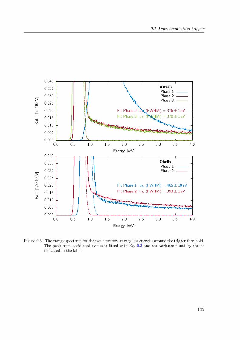
9.1 Data acquisition trigger
0.000
0.005
0.010
0.015
0.020
0.025
0.030
0.035
0.040
0.0 0.5 1.0 1.5 2.0 2.5 3.0 3.5 4.0
Rat
e[1
/s/1
0eV
]
Energy [keV]
Phase 1Phase 2Phase 3
Asterix
Fit Phase 2: σN (FWHM) = 376± 1 eV
Fit Phase 3: σN (FWHM) = 370± 1 eV
0.000
0.005
0.010
0.015
0.020
0.025
0.030
0.035
0.040
0.0 0.5 1.0 1.5 2.0 2.5 3.0 3.5 4.0
Rat
e[1
/s/1
0eV
]
Energy [keV]
Phase 1Phase 2
Obelix
Fit Phase 1: σN (FWHM) = 485± 10 eV
Fit Phase 2: σN (FWHM) = 393± 1 eV
Figure 9.6: The energy spectrum for the two detectors at very low energies around the trigger threshold.The peak from accidental events is fitted with Eq. 9.2 and the variance found by the fitindicated in the label.
135
9 Measurements near the trigger threshold
The energy spectra near the threshold for the two detectors in the different configurationsare represented in Fig. 9.6. The spectral shape close to the threshold of Asterix in its firstconfiguration deviates strongly from the other configurations and the count rate increasesalready at energies of around 4 keV. The events that make up the difference between this andthe other spectra have been investigated and are not related to electronics noise, but havebeen found to be normal single site events. The most probable explanation, thus, is thatthese events originate from a contamination in the cryostat close to the point contact andpenetrate through the point contact or the passivation layer into the detector. Because of theadditional contribution the threshold level for this measurement has been chosen too high andthe real onset of the noise peak can not be seen. Accordingly, it is not possible to comparethis configuration with the later ones.
The remaining spectra follow the expected behavior with roughly constant signal level fromCompton backgrounds that are surpassed at low energies by the peaks from accidentally trig-gered noise events. The data near the threshold have been fitted as described in the previoussection and the respective value of σN are indicated in the figure. The values found for σN areclose to the values for the equivalent noise charge at a shaping time of 1.2µs indicated in Fig. 8.4and Fig. 8.5. This explains why the difference between the second and third configuration ofAsterix is basically not visible – the improvement in the equivalent noise charge between thetwo configuration is also small. The energy threshold for these two configurations is roughly∼ 850 eV at an accidental noise count rate of 0.1 counts/s above the energy threshold.
The effect of the point contact size on the energy threshold, however, can be observed betweenthe two configurations of Obelix. The improvement in noise between the two configurationsof this detector is large enough so that also an improvement in the energy threshold can beobserved. The energy threshold shifts between the two configurations from (1105 ± 17) eV to(906± 6) eV at an accidental noise count rate of 0.1 counts/s above the energy threshold. Theratio of both reflects perfectly the predictions of Eq. 9.1, from which a relation between thetwo configurations can be derived:
d1
d2=σ1
σ2=
465.2 eV
385.8 eV∼ 1.21. (9.3)
The improvement in energy resolution therefore indeed translates directly into an improvementin the width of the energy threshold.
9.2 Application in physics research
The experiments with the two detectors were performed at ground level and high back-grounds from cosmic radiation and the surround of the order of 2 × 10⁵ counts/keV/kg/dayare observed. In typical low background experiments this number is reduced to the order of1 count/keV/kg/day in the low energy region. It was proven by group members [117] thatbackground levels below this value are accessible even at a shallow depth, such as it is requirednear a reactor site. It thus is important to know which energy thresholds can be obtained atthese background levels.
136
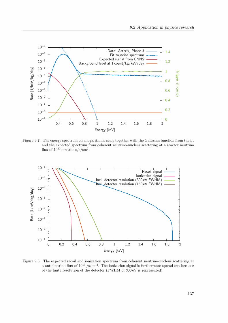
9.2 Application in physics research
10−1
10+0
10+1
10+2
10+3
10+4
10+5
10+6
10+7
10+8
10+9
0.4 0.6 0.8 1 1.2 1.4 1.6 1.8 20
0.2
0.4
0.6
0.8
1
1.2
1.4
Rat
e[1
/keV
/kg/
day
]
Trigger
efficien
cy
Energy [keV]
Data: Asterix, Phase 3Fit to noise spectrum
Expected signal from CNNSBackground level at 1 count/kg/keV/day
Figure 9.7: The energy spectrum on a logarithmic scale together with the Gaussian function from the fitand the expected spectrum from coherent neutrino-nucleus scattering at a reactor neutrinoflux of 1013 neutrinos/s/sm2.
10−1
10+0
10+1
10+2
10+3
10+4
10+5
10+6
0 0.2 0.4 0.6 0.8 1 1.2 1.4 1.6 1.8 2
Rat
e[1
/keV
/kg/
day
]
Energy [keV]
Recoil signalIonization signal
Incl. detector resolution (300 eV FWHM)Incl. detector resolution (150 eV FWHM)
Figure 9.8: The expected recoil and ionization spectrum from coherent neutrino-nucleus scattering ata antineutrino flux of 1013 /s/cm2. The ionization signal is furthermore spread out becauseof the finite resolution of the detector (FWHM of 300 eV is represented).
137
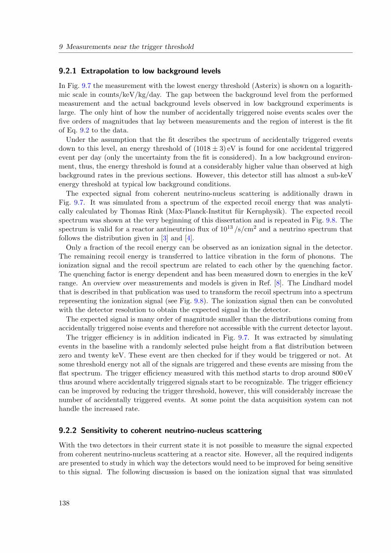
9 Measurements near the trigger threshold
9.2.1 Extrapolation to low background levels
In Fig. 9.7 the measurement with the lowest energy threshold (Asterix) is shown on a logarith-mic scale in counts/keV/kg/day. The gap between the background level from the performedmeasurement and the actual background levels observed in low background experiments islarge. The only hint of how the number of accidentally triggered noise events scales over thefive orders of magnitudes that lay between measurements and the region of interest is the fitof Eq. 9.2 to the data.
Under the assumption that the fit describes the spectrum of accidentally triggered eventsdown to this level, an energy threshold of (1018 ± 3) eV is found for one accidental triggeredevent per day (only the uncertainty from the fit is considered). In a low background environ-ment, thus, the energy threshold is found at a considerably higher value than observed at highbackground rates in the previous sections. However, this detector still has almost a sub-keVenergy threshold at typical low background conditions.
The expected signal from coherent neutrino-nucleus scattering is additionally drawn inFig. 9.7. It was simulated from a spectrum of the expected recoil energy that was analyti-cally calculated by Thomas Rink (Max-Planck-Institut fur Kernphysik). The expected recoilspectrum was shown at the very beginning of this dissertation and is repeated in Fig. 9.8. Thespectrum is valid for a reactor antineutrino flux of 1013 /s/cm2 and a neutrino spectrum thatfollows the distribution given in [3] and [4].
Only a fraction of the recoil energy can be observed as an ionization signal in the detector.The remaining recoil energy is transferred to lattice vibration in the form of phonons. Theionization signal and the recoil spectrum are related to each other by the quenching factor.The quenching factor is energy dependent and has been measured down to energies in the keVrange. An overview over measurements and models is given in Ref. [8]. The Lindhard modelthat is described in that publication was used to transform the recoil spectrum into a spectrumrepresenting the ionization signal (see Fig. 9.8). The ionization signal then can be convolutedwith the detector resolution to obtain the expected signal in the detector.
The expected signal is many order of magnitude smaller than the distributions coming fromaccidentally triggered noise events and therefore not accessible with the current detector layout.
The trigger efficiency is in addition indicated in Fig. 9.7. It was extracted by simulatingevents in the baseline with a randomly selected pulse height from a flat distribution betweenzero and twenty keV. These event are then checked for if they would be triggered or not. Atsome threshold energy not all of the signals are triggered and these events are missing from theflat spectrum. The trigger efficiency measured with this method starts to drop around 800 eVthus around where accidentally triggered signals start to be recognizable. The trigger efficiencycan be improved by reducing the trigger threshold, however, this will considerably increase thenumber of accidentally triggered events. At some point the data acquisition system can nothandle the increased rate.
9.2.2 Sensitivity to coherent neutrino-nucleus scattering
With the two detectors in their current state it is not possible to measure the signal expectedfrom coherent neutrino-nucleus scattering at a reactor site. However, all the required indigentsare presented to study in which way the detectors would need to be improved for being sensitiveto this signal. The following discussion is based on the ionization signal that was simulated
138
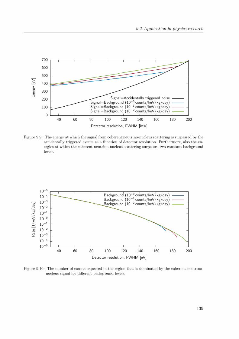
9.2 Application in physics research
0
100
200
300
400
500
600
700
40 60 80 100 120 140 160 180 200
En
ergy
[eV
]
Detector resolution, FWHM [keV]
Signal=Accidentally triggered noiseSignal=Background (10+0 counts/keV/kg/day)Signal=Background (10−1 counts/keV/kg/day)Signal=Background (10−2 counts/keV/kg/day)
Figure 9.9: The energy at which the signal from coherent neutrino-nucleus scattering is surpassed by theaccidentally triggered events as a function of detector resolution. Furthermore, also the en-ergies at which the coherent neutrino-nucleus scattering surpasses two constant backgroundlevels.
10−5
10−4
10−3
10−2
10−1
10+0
10+1
10+2
10+3
10+4
10+5
40 60 80 100 120 140 160 180 200
Rat
e[1
/keV
/kg/
day
]
Detector resolution, FWHM [eV]
Background (10+0 counts/keV/kg/day)Background (10−1 counts/keV/kg/day)Background (10−2 counts/keV/kg/day)
Figure 9.10: The number of counts expected in the region that is dominated by the coherent neutrino-nucleus signal for different background levels.
139
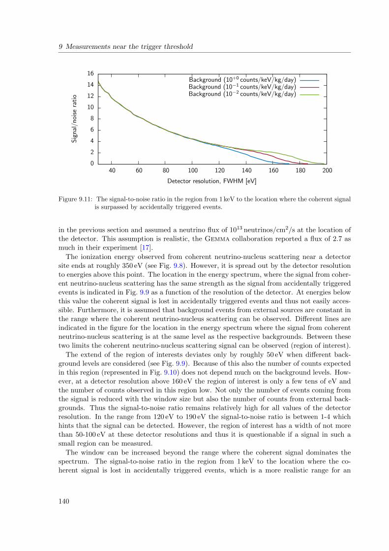
9 Measurements near the trigger threshold
0
2
4
6
8
10
12
14
16
40 60 80 100 120 140 160 180 200
Sig
nal
/noi
sera
tio
Detector resolution, FWHM [eV]
Background (10+0 counts/keV/kg/day)Background (10−1 counts/keV/kg/day)Background (10−2 counts/keV/kg/day)
Figure 9.11: The signal-to-noise ratio in the region from 1 keV to the location where the coherent signalis surpassed by accidentally triggered events.
in the previous section and assumed a neutrino flux of 1013 neutrinos/cm2/s at the location ofthe detector. This assumption is realistic, the Gemma collaboration reported a flux of 2.7 asmuch in their experiment [17].
The ionization energy observed from coherent neutrino-nucleus scattering near a detectorsite ends at roughly 350 eV (see Fig. 9.8). However, it is spread out by the detector resolutionto energies above this point. The location in the energy spectrum, where the signal from coher-ent neutrino-nucleus scattering has the same strength as the signal from accidentally triggeredevents is indicated in Fig. 9.9 as a function of the resolution of the detector. At energies belowthis value the coherent signal is lost in accidentally triggered events and thus not easily acces-sible. Furthermore, it is assumed that background events from external sources are constant inthe range where the coherent neutrino-nucleus scattering can be observed. Different lines areindicated in the figure for the location in the energy spectrum where the signal from coherentneutrino-nucleus scattering is at the same level as the respective backgrounds. Between thesetwo limits the coherent neutrino-nucleus scattering signal can be observed (region of interest).
The extend of the region of interests deviates only by roughly 50 eV when different back-ground levels are considered (see Fig. 9.9). Because of this also the number of counts expectedin this region (represented in Fig. 9.10) does not depend much on the background levels. How-ever, at a detector resolution above 160 eV the region of interest is only a few tens of eV andthe number of counts observed in this region low. Not only the number of events coming fromthe signal is reduced with the window size but also the number of counts from external back-grounds. Thus the signal-to-noise ratio remains relatively high for all values of the detectorresolution. In the range from 120 eV to 190 eV the signal-to-noise ratio is between 1-4 whichhints that the signal can be detected. However, the region of interest has a width of not morethan 50-100 eV at these detector resolutions and thus it is questionable if a signal in such asmall region can be measured.
The window can be increased beyond the range where the coherent signal dominates thespectrum. The signal-to-noise ratio in the region from 1 keV to the location where the co-herent signal is lost in accidentally triggered events, which is a more realistic range for an
140
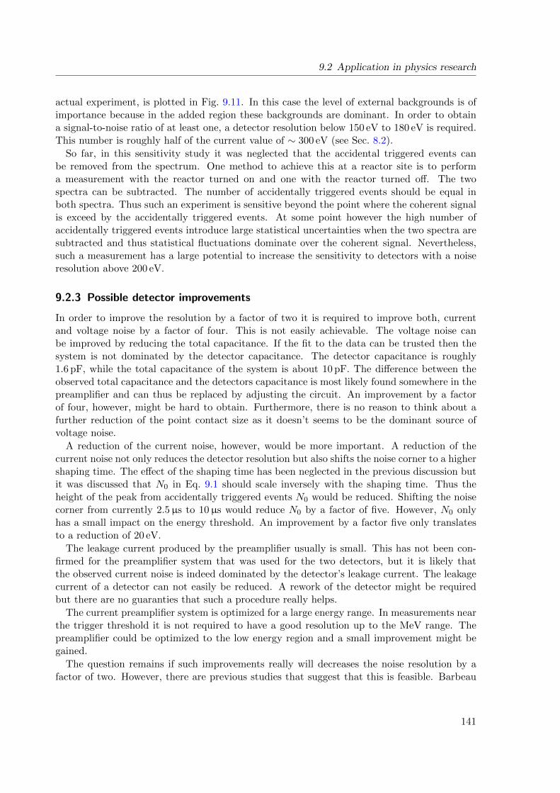
9.2 Application in physics research
actual experiment, is plotted in Fig. 9.11. In this case the level of external backgrounds is ofimportance because in the added region these backgrounds are dominant. In order to obtaina signal-to-noise ratio of at least one, a detector resolution below 150 eV to 180 eV is required.This number is roughly half of the current value of ∼ 300 eV (see Sec. 8.2).
So far, in this sensitivity study it was neglected that the accidental triggered events canbe removed from the spectrum. One method to achieve this at a reactor site is to performa measurement with the reactor turned on and one with the reactor turned off. The twospectra can be subtracted. The number of accidentally triggered events should be equal inboth spectra. Thus such an experiment is sensitive beyond the point where the coherent signalis exceed by the accidentally triggered events. At some point however the high number ofaccidentally triggered events introduce large statistical uncertainties when the two spectra aresubtracted and thus statistical fluctuations dominate over the coherent signal. Nevertheless,such a measurement has a large potential to increase the sensitivity to detectors with a noiseresolution above 200 eV.
9.2.3 Possible detector improvements
In order to improve the resolution by a factor of two it is required to improve both, currentand voltage noise by a factor of four. This is not easily achievable. The voltage noise canbe improved by reducing the total capacitance. If the fit to the data can be trusted then thesystem is not dominated by the detector capacitance. The detector capacitance is roughly1.6 pF, while the total capacitance of the system is about 10 pF. The difference between theobserved total capacitance and the detectors capacitance is most likely found somewhere in thepreamplifier and can thus be replaced by adjusting the circuit. An improvement by a factorof four, however, might be hard to obtain. Furthermore, there is no reason to think about afurther reduction of the point contact size as it doesn’t seems to be the dominant source ofvoltage noise.
A reduction of the current noise, however, would be more important. A reduction of thecurrent noise not only reduces the detector resolution but also shifts the noise corner to a highershaping time. The effect of the shaping time has been neglected in the previous discussion butit was discussed that N0 in Eq. 9.1 should scale inversely with the shaping time. Thus theheight of the peak from accidentally triggered events N0 would be reduced. Shifting the noisecorner from currently 2.5µs to 10µs would reduce N0 by a factor of five. However, N0 onlyhas a small impact on the energy threshold. An improvement by a factor five only translatesto a reduction of 20 eV.
The leakage current produced by the preamplifier usually is small. This has not been con-firmed for the preamplifier system that was used for the two detectors, but it is likely thatthe observed current noise is indeed dominated by the detector’s leakage current. The leakagecurrent of a detector can not easily be reduced. A rework of the detector might be requiredbut there are no guaranties that such a procedure really helps.
The current preamplifier system is optimized for a large energy range. In measurements nearthe trigger threshold it is not required to have a good resolution up to the MeV range. Thepreamplifier could be optimized to the low energy region and a small improvement might begained.
The question remains if such improvements really will decreases the noise resolution by afactor of two. However, there are previous studies that suggest that this is feasible. Barbeau
141
9 Measurements near the trigger threshold
et al. reported a PCGe detector with a resolution of 140 eV [2]. There detector is of a verysimilar design as those studied in this dissertation so there is no practical reason why such aresolution should not be reached.
142
10 Conclusion
Discourse surrounding future large scale germanium detector based experiments has gainedattention in academia. Currently the largest experiments working with germanium detectorssuch as Gerda utilize not more than 30-40 kg of germanium. Many scientists in this fieldagree that an experiment of the order of several 100 kg or tons of germanium is necessary toadvance research on neutrinoless double beta decay and dark matter. Thus, it is doubtfulthat the interest in germanium detectors, especially that for point contact germanium (PCGe)detectors, will subside. However, building an experiment of this order of magnitude is connectedwith many technological (electronics, radio purity, etc.) and logistical (production, storageand handling of large amounts of germanium detectors) pitfalls. Furthermore, the costs for anexperiment on this scale would be extensive and it would require a minimum of a decade toobtain crucial results. Nevertheless, given that the technology is not going to disappear anytime soon, it is vital to understand PCGe detectors beyond the current limitations.
The problems related to a large scale experiment do not arise in experiments near a nuclearreactor. For instance only 1-10 kg of germanium detectors are sufficient to explore the not yetobserved coherent neutrino-nucleus scattering at a nuclear reactor. Such an experiment couldbe constructed in a foreseeable time frame and would not require a large collaboration. Thisdissertation mainly focuses on the potential of PCGe detectors in such an application, however,not exclusively.
The PCGe detector technology was explored with a commercially available detector type,the broad energy germanium detector (BEGe) produced by Canberra N.V., Olen, Belgium.The successive modification of a single germanium crystal removes the main systematics ofa study of the point contact size – variability in the quality of the material. For this study,two almost identical detectors of roughly 760 g were used and allowed for a comparison of theobtained results. The characterization of the detectors with different point contact sizes led tothe following main results:
• It has been possible to experimentally establish a link between the size of the pointcontact and noise from electronics. The FWHM noise resolution has been measured tobe (349 ± 2) eV FWHM at 8.4 mm, (311 ± 2) eV FWHM at 5.0 mm and (299 ± 2) eVFWHM at 2.5 mm point contact radius for the first detector. Similar improvements havebeen observed for the second detector (from (408±1) eV FWHM at 8.2 mm to (336±2) eVFWHM at 5.2 mm).
• Two simple models for the capacitance as a function of the point contact radius weretested. The model, with the capacitance being proportional to the area of the pointcontact and not the radius, describes the data better. The detector is thus close to aparallel plate capacitor. The capacitance of the detector is then given as Cd = εrε0πr
2/h,with the vacuum permittivity ε0 = 8.85×10⁻¹² F/m and the relative permittivity εr = 16in germanium. This model predicts a capacitance of 1.6 pF for the smallest tested pointcontact size.
143
10 Conclusion
• Thanks to an improvement in noise the energy resolution of the 59.5 keV γ-ray line im-proved continuously with a reduction in point contact size from (477±1) eV to (438±1) eVFWHM. As expected, the resolution at 1332.5 keV and 2614.5 keV remained unaffectedfor one detector (∼ 1.58 keV and ∼ 2.3 keV FWHM, respectively) and improved slightlyfor the second detector (to ∼ 1.70 keV and ∼ 2.59 FWHM). This is in agreement withexpectations; the dominant contribution to the resolution at high energy is from fluctu-ations in the number of charge carriers created in the energy deposition.
• The pulse shape discrimination efficiency is defined as the survival fraction in the singleescape peak (SEP) at 2103.5 keV with respect to 90% acceptance in the double escapepeak (DEP) at 1592.5 keV. A good pulse shape discrimination method removes most ofthe background like events (multi site events) in the SEP while signal like events (singlesite event) in the DEP must be conserved. The size of the point contact affects the electricfields, thus, the drift of charge carriers in the detector and the shape of the pulses inducedinto the electrode. The pulse shape discrimination efficiency improves from (12.2±0.2)%to (7.7 ± 0.2)% and to (5.2 ± 0.1)% when going from the largest to the smallest pointcontact size in the first detector. The second detector improves from (14.5 ± 0.4)% to(7.7± 0.2)%.
• The number of accidentally triggered events from noise fluctuations above a certain dis-crimination level d follows, as predicted, the relation:
N(d) = N0 exp
(−d2
2σ2N
), (10.1)
with σN being the noise resolution and N0 the number of counts at zero discriminationlevel. At a typical background rate of a low level experiment (1 count/kg/keV/day) anenergy threshold of approximately 1 keV is predicted.
In order to find the most optimal width between the two electrodes of a PCGe detector at agiven point contact size, simulations were conducted. For this purpose, the ADL3 software [92]was extended, amongst other things, with models of the two detectors and new algorithms forthe electric field calculation. The high performance of the two detectors confirmed the validityof this procedure. The library was further used during the characterization of the detectors:
• Measurements with collimated sources that induce events close to the surface of the de-tector are compared with simulations. Qualitative agreement has been observed betweenmeasurements from various locations and simulations in the position of the 59.5 keV γ-ray line (relative to a reference measurement) and the rise time (2− 70%). The shape ofthe pulse does not entirely agree and cannot be explained by simplifications used in thesimulation. This suggests that the electric field within the detectors was not simulatedcorrectly. Deviations are most likely caused by an insufficient description of the impurityconcentration distribution throughout the detector volume.
Good signal processing techniques are as important as a good detector fabrication to achievea high performance with germanium detectors. The existing program GEANA [83] was tweakedand extended to fit the requirements of the analysis presented. The program contains many
144
traditional but also some new filter routines. This dissertation, furthermore, carefully evalu-ated the performance of the different filter techniques that are implemented in GEANA. Theevaluation found the following:
• The novel ballistic deficit correction method is capable of removing deterioration causedby variability in the shape of pulses at energies above 200 keV. So the γ-ray line at1332.5 keV was improved from (1.82± 0.01) keV to (1.61± 0.01) keV.
• At energies below 200 keV a ballistic deficit correction is not required, instead, it is morebeneficial to use a cusp like filter at these energies to find the best signal-to-noise ratio.The presented rounded-top cusp filter improved the resolution at these energies wellbeyond the specification of the manufacture of the detectors.
• A data set that ranges from a few keV to a few MeV can be processed thanks to theballistic deficit correction with a single shaping time without any major loss in resolution.Between 59.5 keV and 1332.5 keV the loss in resolution compared to an analysis, that findsthe best filter for each γ-ray line individually is less than 40 eV.
• The Fano factor is nearly constant over the range 59.5 keV to 1332.5 keV, however, itslightly increase at higher energies. Two presented methods found consistent resultswhen the Fano factor was assumed to be constant, the better result is 0.1076 ± 0.0005.The first method consists of a constant fit to the values of the Fano factor that werecalculated at individual γ-ray lines. The second method fits the function describing theenergy dependence of the energy resolution to an energy spectrum that was evaluatedwith a single shaping time.
For the presented study a large amount of data were collected; some could not be analyzed.These data still offer some potential for interesting investigations. Furthermore, it might alsobe required to gather some additional data. Some further topics are:
• A careful evaluation of the details of the collimated measurements along the surface ofthe detectors can be used to refine the model of impurity concentration gradients in thedetectors. This should finally produce a good match between the simulation and dataand could also be applied to the data presented in [63].
• With a neutron source (252Cf) the 10.4 keV γ-ray line from isomer 71mGe deexcitationswas induced. This line is an appropriate proxy for signal like events in the low energyregion. This region is dominated by slow pulses, which have a special shape that canbe distinguished from those expected from coherent neutrino-nucleus scattering, neu-trino magnetic moment or dark matter interactions. The 10.4 keV γ-ray line can be usedto study the efficiency of different pulse shape discrimination methods at low energies.Such methods can be of particular importance to reach background level of less than1 count/keV/kg/day that would facilitate a potential coherent neutrino-nucleus exper-iment. Such a study could be further extended with the purchase of a thin entrancewindow to measure γ-ray lines at this range of energy.
• The measurements were conducted above ground without a veto system against signalsfrom cosmic radiation and without extensive efforts to shield the detector from exter-nal backgrounds. Contaminations from these sources in low background experiments
145
10 Conclusion
are roughly 5 orders of magnitude smaller. The background composition and energythreshold at these background levels have not been studied in this dissertation.
The presented results, particularly those from the characterization measurements of the twodetectors, have some important implications. The results on the pulse shape discriminationof the two detectors is relevant for potential large scale experiments that try to measure neu-trinoless beta decay. A small point contact size in the order of 5 mm radius or less helps toimprove the pulse shape discrimination performance of PCGe detectors. This might help tocontrol the variability observed in Ref. [63].
The obtained noise resolution is still too large to measure coherent neutrino-nucleus scat-tering. The sensitivity study, that was presented, shows that a FWHM noise resolution of lessthan 150−180 eV must be reached in order to detect the coherent signal. Thus, it is inevitableto improve the detector’s resolution before such an experiment can be envisioned. An upgradeor exchange of the electronics certainly is capable of slightly improving the resolution, par-ticularly in regards to the voltage noise. However, it is doubtful that it will be sufficient. Inorder to reach the required resolution the current noise must be reduced. The electrical com-ponents used in the preamplifier only make up a small contribution to the observed currentnoise. The measured current noise must be dominated by the detector’s leakage current. Thisnoise source cannot simply be removed by an electronics upgrade as leakage currents are aproperty of the detectors bulk and surface. Reworking the groove might help, but ultimatelythe only way to efficiently remove the leakage currents is by using other detectors with a lowerleakage current. The most promising way of achieving better noise conditions is to move tosmaller detectors. Reducing the size to 500 g has been shown to considerably improve the noise.This dissertation has been limited to the detectors of a single manufacturer. Other companieshave similar products with a slightly modified design, that might be better suited for such anapplication. Low background techniques are additionally vital to the successful conduction ofa coherent neutrino-nucleus experiment. Background levels of 1 count/kg/keV/day need to beachieved to measure coherent neutrino-nucleus scattering. These levels of background recentlyhave been obtained for a germanium detector operated at shallow depth of a few meters rockoverburden in the energy range 40-50 keV [117]. Combined with pulse shape discriminationmethods it seems reasonable to achieve the required background levels. Studying pulse shapediscrimination methods in the low energy region and at low background levels is amongst thenext milestones towards the realization of a coherent neutrino-nucleus scattering experiment.
146
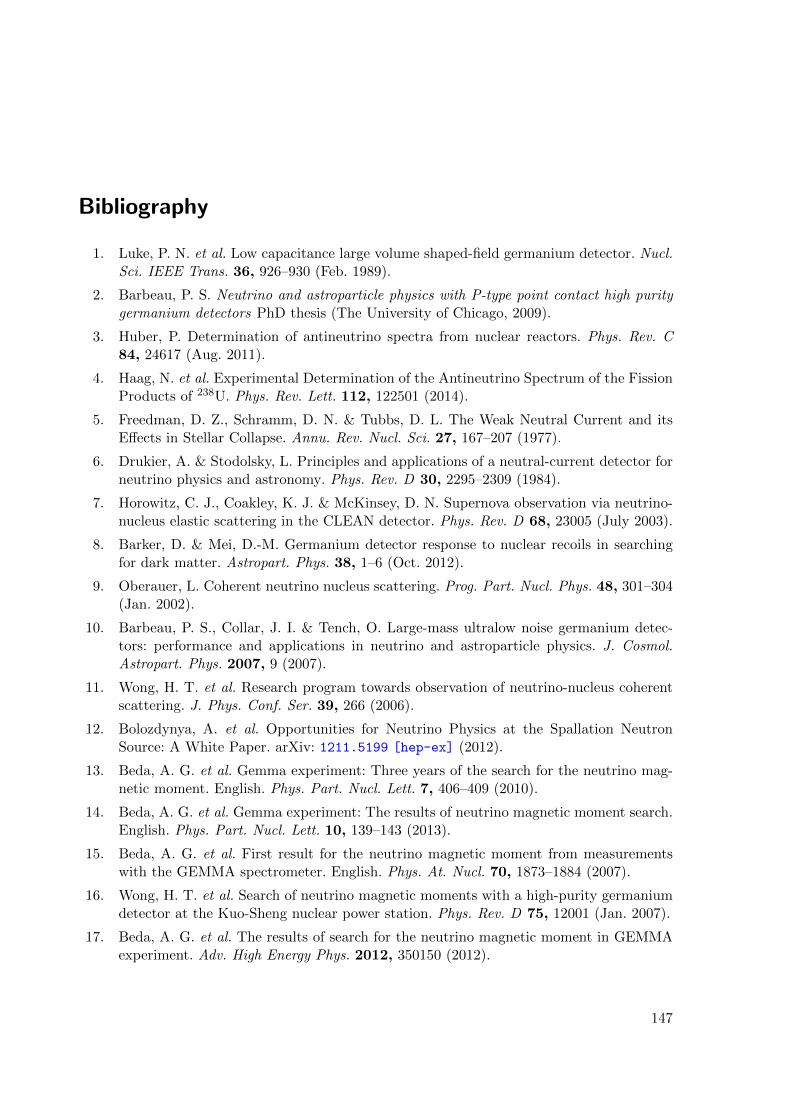
Bibliography
1. Luke, P. N. et al. Low capacitance large volume shaped-field germanium detector. Nucl.Sci. IEEE Trans. 36, 926–930 (Feb. 1989).
2. Barbeau, P. S. Neutrino and astroparticle physics with P-type point contact high puritygermanium detectors PhD thesis (The University of Chicago, 2009).
3. Huber, P. Determination of antineutrino spectra from nuclear reactors. Phys. Rev. C84, 24617 (Aug. 2011).
4. Haag, N. et al. Experimental Determination of the Antineutrino Spectrum of the FissionProducts of 238U. Phys. Rev. Lett. 112, 122501 (2014).
5. Freedman, D. Z., Schramm, D. N. & Tubbs, D. L. The Weak Neutral Current and itsEffects in Stellar Collapse. Annu. Rev. Nucl. Sci. 27, 167–207 (1977).
6. Drukier, A. & Stodolsky, L. Principles and applications of a neutral-current detector forneutrino physics and astronomy. Phys. Rev. D 30, 2295–2309 (1984).
7. Horowitz, C. J., Coakley, K. J. & McKinsey, D. N. Supernova observation via neutrino-nucleus elastic scattering in the CLEAN detector. Phys. Rev. D 68, 23005 (July 2003).
8. Barker, D. & Mei, D.-M. Germanium detector response to nuclear recoils in searchingfor dark matter. Astropart. Phys. 38, 1–6 (Oct. 2012).
9. Oberauer, L. Coherent neutrino nucleus scattering. Prog. Part. Nucl. Phys. 48, 301–304(Jan. 2002).
10. Barbeau, P. S., Collar, J. I. & Tench, O. Large-mass ultralow noise germanium detec-tors: performance and applications in neutrino and astroparticle physics. J. Cosmol.Astropart. Phys. 2007, 9 (2007).
11. Wong, H. T. et al. Research program towards observation of neutrino-nucleus coherentscattering. J. Phys. Conf. Ser. 39, 266 (2006).
12. Bolozdynya, A. et al. Opportunities for Neutrino Physics at the Spallation NeutronSource: A White Paper. arXiv: 1211.5199 [hep-ex] (2012).
13. Beda, A. G. et al. Gemma experiment: Three years of the search for the neutrino mag-netic moment. English. Phys. Part. Nucl. Lett. 7, 406–409 (2010).
14. Beda, A. G. et al. Gemma experiment: The results of neutrino magnetic moment search.English. Phys. Part. Nucl. Lett. 10, 139–143 (2013).
15. Beda, A. G. et al. First result for the neutrino magnetic moment from measurementswith the GEMMA spectrometer. English. Phys. At. Nucl. 70, 1873–1884 (2007).
16. Wong, H. T. et al. Search of neutrino magnetic moments with a high-purity germaniumdetector at the Kuo-Sheng nuclear power station. Phys. Rev. D 75, 12001 (Jan. 2007).
17. Beda, A. G. et al. The results of search for the neutrino magnetic moment in GEMMAexperiment. Adv. High Energy Phys. 2012, 350150 (2012).
147
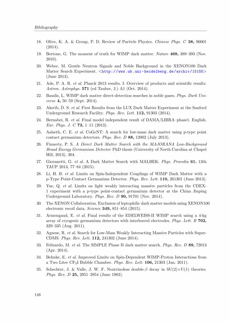
Bibliography
18. Olive, K. A. & Group, P. D. Review of Particle Physics. Chinese Phys. C 38, 90001(2014).
19. Bertone, G. The moment of truth for WIMP dark matter. Nature 468, 389–393 (Nov.2010).
20. Weber, M. Gentle Neutron Signals and Noble Background in the XENON100 DarkMatter Search Experiment. <http://www.ub.uni-heidelberg.de/archiv/15155>(June 2013).
21. Ade, P. A. R. et al. Planck 2013 results. I. Overview of products and scientific results.Astron. Astrophys. 571 (ed Tauber, J.) A1 (Oct. 2014).
22. Baudis, L. WIMP dark matter direct-detection searches in noble gases. Phys. Dark Uni-verse 4, 50–59 (Sept. 2014).
23. Akerib, D. S. et al. First Results from the LUX Dark Matter Experiment at the SanfordUnderground Research Facility. Phys. Rev. Lett. 112, 91303 (2014).
24. Bernabei, R. et al. Final model independent result of DAMA/LIBRA–phase1. English.Eur. Phys. J. C 73, 1–11 (2013).
25. Aalseth, C. E. et al. CoGeNT: A search for low-mass dark matter using p-type pointcontact germanium detectors. Phys. Rev. D 88, 12002 (July 2013).
26. Finnerty, P. S. A Direct Dark Matter Search with the MAJORANA Low-BackgroundBroad Energy Germanium Detector PhD thesis (University of North Carolina at ChapelHill, 2013), 304.
27. Giovanetti, G. et al. A Dark Matter Search with MALBEK. Phys. Procedia 61. 13thTAUP 2013, 77–84 (2015).
28. Li, H. B. et al. Limits on Spin-Independent Couplings of WIMP Dark Matter with ap-Type Point-Contact Germanium Detector. Phys. Rev. Lett. 110, 261301 (June 2013).
29. Yue, Q. et al. Limits on light weakly interacting massive particles from the CDEX-1 experiment with a p-type point-contact germanium detector at the China JinpingUnderground Laboratory. Phys. Rev. D 90, 91701 (Nov. 2014).
30. The XENON Collaboration. Exclusion of leptophilic dark matter models using XENON100electronic recoil data. Science 349, 851–854 (2015).
31. Armengaud, E. et al. Final results of the EDELWEISS-II WIMP search using a 4-kgarray of cryogenic germanium detectors with interleaved electrodes. Phys. Lett. B 702,329–335 (Aug. 2011).
32. Agnese, R. et al. Search for Low-Mass Weakly Interacting Massive Particles with Super-CDMS. Phys. Rev. Lett. 112, 241302 (June 2014).
33. Felizardo, M. et al. The SIMPLE Phase II dark matter search. Phys. Rev. D 89, 72013(Apr. 2014).
34. Behnke, E. et al. Improved Limits on Spin-Dependent WIMP-Proton Interactions froma Two Liter CF3I Bubble Chamber. Phys. Rev. Lett. 106, 21303 (Jan. 2011).
35. Schechter, J. & Valle, J. W. F. Neutrinoless double-β decay in SU(2)×U(1) theories.Phys. Rev. D 25, 2951–2954 (June 1982).
148
Bibliography
36. Rodejohann, W. Neutrino-less Double Beta Decay and Particle Physics. Int. J. Mod.Phys. E 20, 1833–1930 (2011).
37. Agostini, M. et al. Results on Neutrinoless Double-β Decay of 76Ge from Phase I of theGERDA Experiment. Phys. Rev. Lett. 111, 122503 (Sept. 2013).
38. The EXO-200 Collaboration. Search for Majorana neutrinos with the first two years ofEXO-200 data. Nature 510, 229–234 (June 2014).
39. Gando, A. et al. Limit on Neutrinoless ββ Decay of 136Xe from the First Phase ofKamLAND-Zen and Comparison with the Positive Claim in 76Ge. Phys. Rev. Lett. 110,62502 (Feb. 2013).
40. Knopfle, K. T. Upgrade of the GERDA experiment. PoS. TIPP2014, 109 (2014).
41. Abgrall, N. et al. The Majorana Demonstrator Neutrinoless Double-Beta Decay Exper-iment. Adv.High Energy Phys. 2014, 365432 (2014).
42. Leo, W. R. Techniques for nuclear and particle physics experiments : A How-to Approachisbn: 3540572805. doi:10.1119/1.16209 (1990).
43. Berger, M. J. et al. ESTAR : Stopping-Power and Range Tables for Electrons, Protons,and Helium Ions. NIST. <http://www.nist.gov/pml/data/star/index.cfm> (2011).
44. Berger, M. J. et al. XCOM: photon cross sections database. NIST Stand. Ref. Database8, 87–3597 (1998).
45. Compton, A. H. A Quantum Theory of the Scattering of X-rays by Light Elements.Phys. Rev. 21, 483–502 (1923).
46. Klein, O. & Nishina, T. Uber die Streuung von Strahlung durch freie Elektronen nachder neuen relativistischen Quantendynamik von Dirac. Zeitschrift fur Phys. 52, 853–868(1929).
47. Knoll, G. F. Radiation Detection and Measurement isbn: 9780470131480 (John Wiley& Sons, Inc., 2010).
48. Spieler, H. Semiconductor Detector Systems isbn: 9780198527848. doi:10.1093/acprof:oso/9780198527848.001.0001 (Oxford University Press, Oxford, 2005).
49. Shockley, W. Currents to conductors induced by a moving point charge. J. Appl. Phys.9, 635–636 (1938).
50. Ramo, S. Currents Induced by Electron Motion. Proc. IRE 27. doi:10.1109/JRPROC.1939.228757 (Sept. 1939).
51. He, Z. Review of the Shockley–Ramo theorem and its application in semiconductorgamma-ray detectors. Nucl. Instruments Methods Phys. Res. Sect. A Accel. Spectrome-ters, Detect. Assoc. Equip. 463, 250–267 (May 2001).
52. Kim, H. et al. An extended proof of the Ramo-Shockley theorem. Solid. State. Electron.34, 1251–1253 (1991).
53. Bruyneel, B. Characterization of Segmented Large Volume, High Purity GermaniumDetectors PhD thesis (Universitat zu Koln, 2006), 137. <http://kups.ub.uni-koeln.de/id/eprint/1858>.
149
Bibliography
54. Keyser, R. M. & Raudorf, T. W. Germanium radiation detector manufacturing: Pro-cess and advances. Nucl. Instruments Methods Phys. Res. Sect. A Accel. Spectrometers,Detect. Assoc. Equip. 286, 357–363 (Jan. 1990).
55. Uppal, S. et al. Ion-implantation and diffusion behaviour of boron in germanium. Phys.B Condens. Matter 308-310, 525–528 (Dec. 2001).
56. Sher, A. H. Lithium-Ion Drift Mobility in Germanium. J. Appl. Phys. 40, 2600 (1969).
57. Martin, G. N. et al. Improving Germanium Detector Resolution and Reliability tech.rep. (CANBERRA and Pacific Northwest National Laboratory, 2008), 7. <http://www.dtic.mil/cgi-bin/GetTRDoc?AD=ADA516274>.
58. Fano, U. Ionization Yield of Radiations. II. The Fluctuations of the Number of Ions.Phys. Rev. 72, 26–29 (1947).
59. Van Roosbroeck, W. Theory of the yield and fano factor of electron-hole pairs generatedin semiconductors by high-energy particles. Phys. Rev. 139 (1965).
60. Devanathan, R. et al. Signal variance in gamma-ray detectors-A review. Nucl. Instru-ments Methods Phys. Res. Sect. A Accel. Spectrometers, Detect. Assoc. Equip. 565, 637–649 (2006).
61. Croft, S. & Bond, D. A determination of the Fano factor for germanium at 77.4 K frommeasurements of the energy resolution of a 113 cm3 HPGe gamma-ray spectrometertaken over the energy range from 14 to 6129 keV. Int. J. Radiat. Appl. Instrumentation.Part A. Appl. Radiat. Isot. 42, 1009–1014 (Jan. 1991).
62. Perotti, F. & Fiorini, C. Observed energy dependence of Fano factor in silicon at hard X-ray energies. Nucl. Instruments Methods Phys. Res. Sect. A Accel. Spectrometers, Detect.Assoc. Equip. 423, 356–363 (Mar. 1999).
63. Agostini, M. et al. Production, characterization and operation of 76Ge enriched BEGedetectors in GERDA. English. Eur. Phys. J. C 75, 1–22 (2015).
64. Aalseth, C. et al. Astroparticle physics with a customized low-background broad energyGermanium detector. Nucl. Instruments Methods Phys. Res. Sect. A Accel. Spectrome-ters, Detect. Assoc. Equip. 652, 692–695 (Oct. 2011).
65. Aguayo, E. et al. Characteristics of signals originating near the lithium-diffused N+contact of high purity germanium p-type point contact detectors. Nucl. InstrumentsMethods Phys. Res. Sect. A Accel. Spectrometers, Detect. Assoc. Equip. 701, 176–185(Feb. 2013).
66. Canberra Industries Inc. <http://www.canberra.com> (visited on 07/26/2015).
67. ORTEC. <http://www.ortec-online.com> (visited on 07/26/2015).
68. Baltic Scientific Instruments Ltd. <http://www.bsi.lv> (visited on 07/26/2015).
69. Fuller, C. S. & Severiens, J. C. Mobility of impurity ions in germanium and silicon. Phys.Rev. 96, 21–24 (1954).
70. Trumbore, F. A. Solid Solubilities of Impurity Elements in Germanium and Silicon. BellSyst. Tech. J. 39, 205–233 (Jan. 1960).
71. Gaubas, E. & Vanhellemont, J. Comparative Study of Carrier Lifetime Dependence onDopant Concentration in Silicon and Germanium 2007.
150
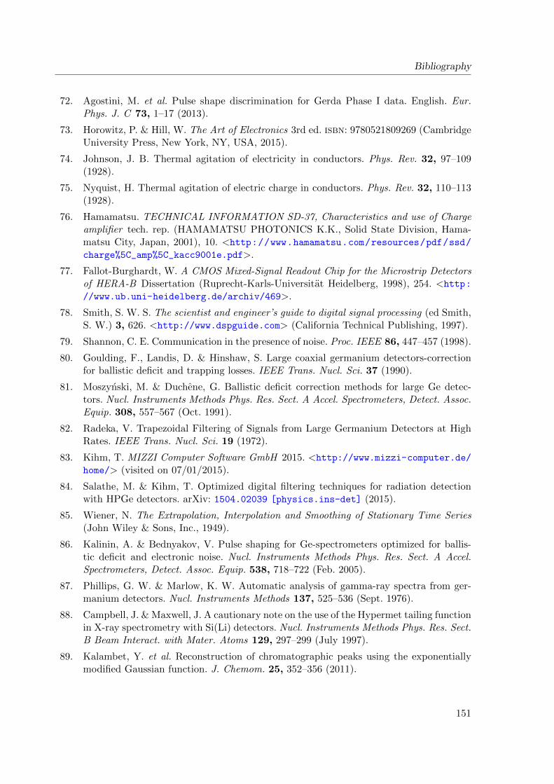
Bibliography
72. Agostini, M. et al. Pulse shape discrimination for Gerda Phase I data. English. Eur.Phys. J. C 73, 1–17 (2013).
73. Horowitz, P. & Hill, W. The Art of Electronics 3rd ed. isbn: 9780521809269 (CambridgeUniversity Press, New York, NY, USA, 2015).
74. Johnson, J. B. Thermal agitation of electricity in conductors. Phys. Rev. 32, 97–109(1928).
75. Nyquist, H. Thermal agitation of electric charge in conductors. Phys. Rev. 32, 110–113(1928).
76. Hamamatsu. TECHNICAL INFORMATION SD-37, Characteristics and use of Chargeamplifier tech. rep. (HAMAMATSU PHOTONICS K.K., Solid State Division, Hama-matsu City, Japan, 2001), 10. <http://www.hamamatsu.com/resources/pdf/ssd/charge%5C_amp%5C_kacc9001e.pdf>.
77. Fallot-Burghardt, W. A CMOS Mixed-Signal Readout Chip for the Microstrip Detectorsof HERA-B Dissertation (Ruprecht-Karls-Universitat Heidelberg, 1998), 254. <http://www.ub.uni-heidelberg.de/archiv/469>.
78. Smith, S. W. S. The scientist and engineer’s guide to digital signal processing (ed Smith,S. W.) 3, 626. <http://www.dspguide.com> (California Technical Publishing, 1997).
79. Shannon, C. E. Communication in the presence of noise. Proc. IEEE 86, 447–457 (1998).
80. Goulding, F., Landis, D. & Hinshaw, S. Large coaxial germanium detectors-correctionfor ballistic deficit and trapping losses. IEEE Trans. Nucl. Sci. 37 (1990).
81. Moszynski, M. & Duchene, G. Ballistic deficit correction methods for large Ge detec-tors. Nucl. Instruments Methods Phys. Res. Sect. A Accel. Spectrometers, Detect. Assoc.Equip. 308, 557–567 (Oct. 1991).
82. Radeka, V. Trapezoidal Filtering of Signals from Large Germanium Detectors at HighRates. IEEE Trans. Nucl. Sci. 19 (1972).
83. Kihm, T. MIZZI Computer Software GmbH 2015. <http://www.mizzi-computer.de/home/> (visited on 07/01/2015).
84. Salathe, M. & Kihm, T. Optimized digital filtering techniques for radiation detectionwith HPGe detectors. arXiv: 1504.02039 [physics.ins-det] (2015).
85. Wiener, N. The Extrapolation, Interpolation and Smoothing of Stationary Time Series(John Wiley & Sons, Inc., 1949).
86. Kalinin, A. & Bednyakov, V. Pulse shaping for Ge-spectrometers optimized for ballis-tic deficit and electronic noise. Nucl. Instruments Methods Phys. Res. Sect. A Accel.Spectrometers, Detect. Assoc. Equip. 538, 718–722 (Feb. 2005).
87. Phillips, G. W. & Marlow, K. W. Automatic analysis of gamma-ray spectra from ger-manium detectors. Nucl. Instruments Methods 137, 525–536 (Sept. 1976).
88. Campbell, J. & Maxwell, J. A cautionary note on the use of the Hypermet tailing functionin X-ray spectrometry with Si(Li) detectors. Nucl. Instruments Methods Phys. Res. Sect.B Beam Interact. with Mater. Atoms 129, 297–299 (July 1997).
89. Kalambet, Y. et al. Reconstruction of chromatographic peaks using the exponentiallymodified Gaussian function. J. Chemom. 25, 352–356 (2011).
151
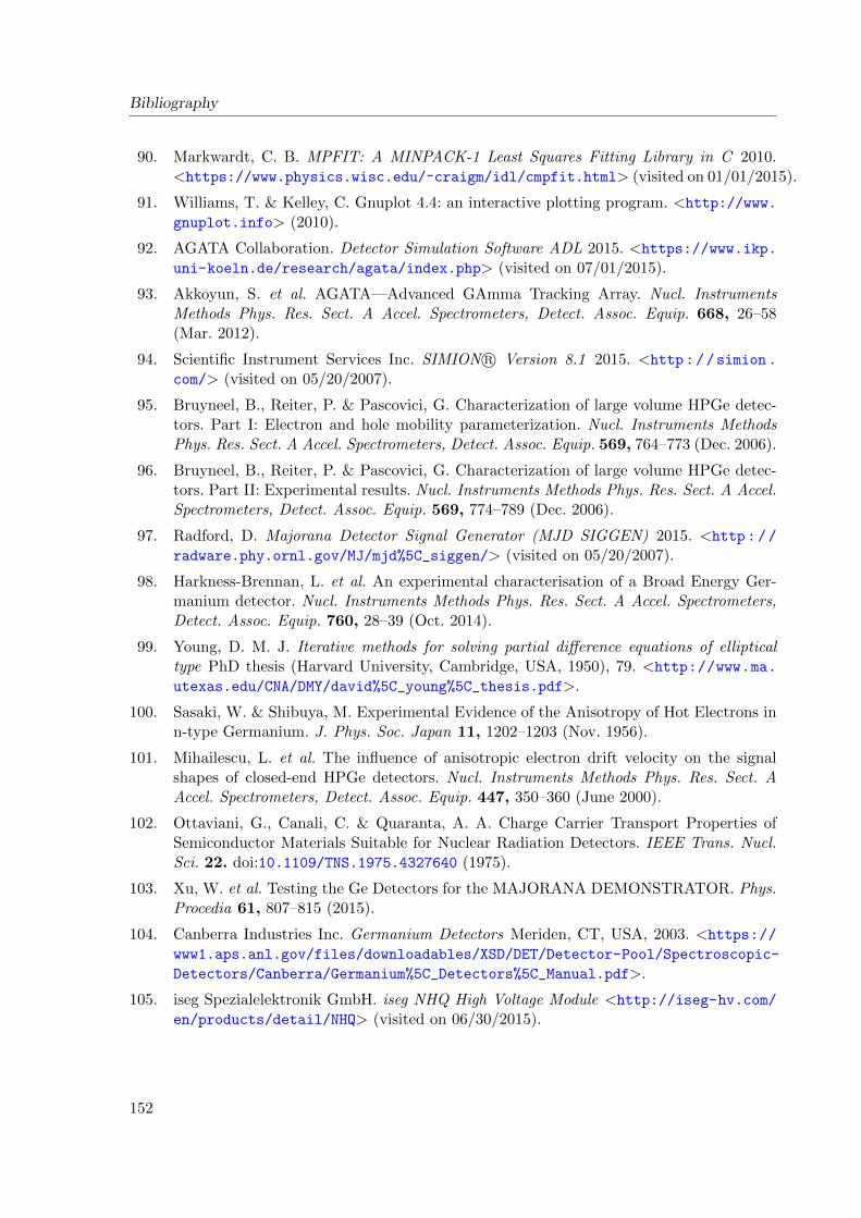
Bibliography
90. Markwardt, C. B. MPFIT: A MINPACK-1 Least Squares Fitting Library in C 2010.<https://www.physics.wisc.edu/~craigm/idl/cmpfit.html> (visited on 01/01/2015).
91. Williams, T. & Kelley, C. Gnuplot 4.4: an interactive plotting program. <http://www.gnuplot.info> (2010).
92. AGATA Collaboration. Detector Simulation Software ADL 2015. <https://www.ikp.uni-koeln.de/research/agata/index.php> (visited on 07/01/2015).
93. Akkoyun, S. et al. AGATA—Advanced GAmma Tracking Array. Nucl. InstrumentsMethods Phys. Res. Sect. A Accel. Spectrometers, Detect. Assoc. Equip. 668, 26–58(Mar. 2012).
94. Scientific Instrument Services Inc. SIMION R© Version 8.1 2015. <http://simion.com/> (visited on 05/20/2007).
95. Bruyneel, B., Reiter, P. & Pascovici, G. Characterization of large volume HPGe detec-tors. Part I: Electron and hole mobility parameterization. Nucl. Instruments MethodsPhys. Res. Sect. A Accel. Spectrometers, Detect. Assoc. Equip. 569, 764–773 (Dec. 2006).
96. Bruyneel, B., Reiter, P. & Pascovici, G. Characterization of large volume HPGe detec-tors. Part II: Experimental results. Nucl. Instruments Methods Phys. Res. Sect. A Accel.Spectrometers, Detect. Assoc. Equip. 569, 774–789 (Dec. 2006).
97. Radford, D. Majorana Detector Signal Generator (MJD SIGGEN) 2015. <http://radware.phy.ornl.gov/MJ/mjd%5C_siggen/> (visited on 05/20/2007).
98. Harkness-Brennan, L. et al. An experimental characterisation of a Broad Energy Ger-manium detector. Nucl. Instruments Methods Phys. Res. Sect. A Accel. Spectrometers,Detect. Assoc. Equip. 760, 28–39 (Oct. 2014).
99. Young, D. M. J. Iterative methods for solving partial difference equations of ellipticaltype PhD thesis (Harvard University, Cambridge, USA, 1950), 79. <http://www.ma.utexas.edu/CNA/DMY/david%5C_young%5C_thesis.pdf>.
100. Sasaki, W. & Shibuya, M. Experimental Evidence of the Anisotropy of Hot Electrons inn-type Germanium. J. Phys. Soc. Japan 11, 1202–1203 (Nov. 1956).
101. Mihailescu, L. et al. The influence of anisotropic electron drift velocity on the signalshapes of closed-end HPGe detectors. Nucl. Instruments Methods Phys. Res. Sect. AAccel. Spectrometers, Detect. Assoc. Equip. 447, 350–360 (June 2000).
102. Ottaviani, G., Canali, C. & Quaranta, A. A. Charge Carrier Transport Properties ofSemiconductor Materials Suitable for Nuclear Radiation Detectors. IEEE Trans. Nucl.Sci. 22. doi:10.1109/TNS.1975.4327640 (1975).
103. Xu, W. et al. Testing the Ge Detectors for the MAJORANA DEMONSTRATOR. Phys.Procedia 61, 807–815 (2015).
104. Canberra Industries Inc. Germanium Detectors Meriden, CT, USA, 2003. <https://www1.aps.anl.gov/files/downloadables/XSD/DET/Detector-Pool/Spectroscopic-
Detectors/Canberra/Germanium%5C_Detectors%5C_Manual.pdf>.
105. iseg Spezialelektronik GmbH. iseg NHQ High Voltage Module <http://iseg-hv.com/en/products/detail/NHQ> (visited on 06/30/2015).
152
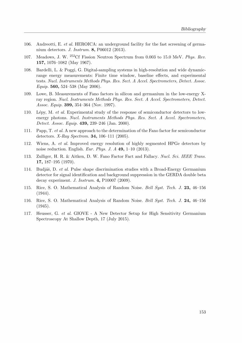
Bibliography
106. Andreotti, E. et al. HEROICA: an underground facility for the fast screening of germa-nium detectors. J. Instrum. 8, P06012 (2013).
107. Meadows, J. W. 252Cf Fission Neutron Spectrum from 0.003 to 15.0 MeV. Phys. Rev.157, 1076–1082 (May 1967).
108. Bardelli, L. & Poggi, G. Digital-sampling systems in high-resolution and wide dynamic-range energy measurements: Finite time window, baseline effects, and experimentaltests. Nucl. Instruments Methods Phys. Res. Sect. A Accel. Spectrometers, Detect. Assoc.Equip. 560, 524–538 (May 2006).
109. Lowe, B. Measurements of Fano factors in silicon and germanium in the low-energy X-ray region. Nucl. Instruments Methods Phys. Res. Sect. A Accel. Spectrometers, Detect.Assoc. Equip. 399, 354–364 (Nov. 1997).
110. Lepy, M. et al. Experimental study of the response of semiconductor detectors to low-energy photons. Nucl. Instruments Methods Phys. Res. Sect. A Accel. Spectrometers,Detect. Assoc. Equip. 439, 239–246 (Jan. 2000).
111. Papp, T. et al. A new approach to the determination of the Fano factor for semiconductordetectors. X-Ray Spectrom. 34, 106–111 (2005).
112. Wiens, A. et al. Improved energy resolution of highly segmented HPGe detectors bynoise reduction. English. Eur. Phys. J. A 49, 1–10 (2013).
113. Zulliger, H. R. & Aitken, D. W. Fano Factor Fact and Fallacy. Nucl. Sci. IEEE Trans.17, 187–195 (1970).
114. Budjas, D. et al. Pulse shape discrimination studies with a Broad-Energy Germaniumdetector for signal identification and background suppression in the GERDA double betadecay experiment. J. Instrum. 4, P10007 (2009).
115. Rice, S. O. Mathematical Analysis of Random Noise. Bell Syst. Tech. J. 23, 46–156(1944).
116. Rice, S. O. Mathematical Analysis of Random Noise. Bell Syst. Tech. J. 24, 46–156(1945).
117. Heusser, G. et al. GIOVE - A New Detector Setup for High Sensitivity GermaniumSpectroscopy At Shallow Depth, 17 (July 2015).
153

Acknowledgements
I’m very thankful to all the people that supported me during the time I spent writing thisthesis:
• First of all I’m incredible grateful to my fiancee, Nicole Vital, who supported me in everyway possible. She was there to motivate me in the times when I lost hope that I wouldcomplete my thesis on time and always found a way to cheer me up. I’m so happy tohave a person like her by my side and feel extremely honored I will marry her soon.
• I would like to thank my two advisers, Dr. Werner Maneschg and Dr. Bernhard Schwin-genheuer, who always had a bit of spare time to give me feedback on my writing, aswell as for the many interesting and enriching discussions about PCGes and my research.Furthermore, I’m indebted to Thomas Kihm, who had no obligations what so ever tohelp me, but was always there to discuss software and programs and inspired many ofthe new ideas presented in this dissertation. He also took his valuable free time to readthrough this thesis.
• I’m thankful to Prof. Dr. Manfred Lindner for his support and the freedom to pursuedifferent topics I found intriguing. Furthermore, I would like to thank Prof. Dr. NorbertHerrmann who accepted the responsibility of being my second referee for this thesis.Notably, Thomas Rink for calculating some important data used in this work, JohannesWelter for reading through the theoretical section and Antoine Collin for all the inspiringdiscussions.
• Thanks also goes to people from the Gerda collaboration as well as the entire Lindnergroup at the Max-Planck-Institut fur Kernphysik, Heidelberg. The exchange with peoplefrom different fields and experiments was very valuable.
• Last but not least I’m grateful to my entire family: My parents, Monika and JosephSalathe, who supported me through my childhood and my studies. This is somethingthat never can be paid back. My sister, Andrea Salathe, for accompany me through somany nice years and for giving me new outlooks on live. My grandmother, Bethli Furler,for always believing in me.
154