DIRECT VOLTAGE CONTROL FOR STAND-ALONE WIND ENERGY CONVERSION SYSTEMS WITH ENERGY...
86
DIRECT VOLTAGE CONTROL FOR STAND-ALONE WIND ENERGY CONVERSION SYSTEMS WITH ENERGY STORAGE by WEI HUANG BSc, Huazhong University of Science and Technology, China, 2005 A thesis presented to Ryerson University in partial fulfillment of the requirements for the degree of Master of Applied Science in the Program of Electrical and Computer Engineering Toronto, Canada © Wei Huang 2008 PROPERTY OF RYERSON UHJVEBSJJY UBBABV
-
Upload
nguyenkhanh -
Category
Documents
-
view
226 -
download
2
Transcript of DIRECT VOLTAGE CONTROL FOR STAND-ALONE WIND ENERGY CONVERSION SYSTEMS WITH ENERGY...

DIRECT VOLTAGE CONTROL FOR STAND-ALONE WIND ENERGY CONVERSION SYSTEMS WITH ENERGY STORAGE
by
WEI HUANG BSc, Huazhong University of Science and Technology, China, 2005
A thesis
presented to Ryerson University
in partial fulfillment of the
requirements for the degree of
Master of Applied Science
in the Program of
Electrical and Computer Engineering
Toronto, Canada © Wei Huang 2008
PROPERTY OF RYERSON UHJVEBSJJY UBBABV

ABSTRACT
Direct Voltage Control for Stand-alone Wind Energy Conversion Systems with Energy
Storage
Wei Huang
Electrical and Computer Engineering
Ryerson University
Toronto 2008
A control method for the stand-alone wind power generation system with induction genera
tor and energy storage devices is proposed in this thesis. A fixed-speed self-excited induction
generator is directly connected to the standalone power system, while battery powered energy
storage devices are employed to balance the system power flow. A DC-AC power converter is
connected between the energy storage device and the standalone power system, which maintains
the voltage and frequency constant. Direct voltage control with current limits is developed for
the converter with dynamic fast response. Mathematical models are developed to analysis the
system performance as well as to design the lead-lag regulators in the control system. The pro
posed system is verified in the simulation and experiment.
III

ACKNOWLEDGMENTS
I wish to express my deep gratitude to my supervisor, Professor Dewei Xu for his support
and the knowledge he shared during my graduate studies at Ryerson University.
I am grateful to Professor Bin Wu, Professor Richard Cheung, Dr. Y ongqiang Lang, and all
fellow students at LEDAR for their useful discussions on my research.
I also wish to share my achievements with my families and my wife Wei Li. I am very
grateful for her understanding and support.
IV

TABLE OF CONTENTS
CHAPTER 1 INTRODUCTION .................................................................................... !
1.1
1.2
1.3
1.4
Wind Energy- Conversion System .................................................................................. 1
Stand-alone Wind Energy- Conversion System ............................................................. 4
Motivation and Objective ............................................................................................... 7
Thesis Outline .................................................................................................................. 8
CHAPTER 2 MODEL DEVELOPMENT FOR THE STANDALONE WECS ..... 10
2.1 Introduction ................................................................................................................... 10
2.2 Wind Turbine Characteristic ...................................................................................•... 11
2.3 Induction Generator Model .......................................................................................... 12
2.4 Inductive Load and Self-Excitation Capacitor Model ............................................... 15
2.5 Energy Storage System Model ..................................................................................... 15
2.6 Standalone WECS Model ............................................................................................. 16
2. 7 Small Signal Model ........................................................................................................ 17
2.8 Conclusions .................................................................................................................... 20
CHAPTER 3 CONTROL OF STANDALONE WECS ............................................. 21
3.1 Introduction ................................................................................................................... 21
3.2 Direct Voltage Control .................................................................................................. 22
3.2.1
3.2.2
Voltage and Frequency Control.. .......................................................................... 22
Direct Voltage Controller Design ......................................................................... 23
3.3 Conclusions .................................................................................................................... 28
CHAPTER 4 SIMULATION AND EXPERIMENTAL RESULTS ......................... 29
4.1 Introduction ................................................................................................................... 29
4.2 Simulation Model ..••.............................•................................................................•.•..... 30
4.3 Simulation Results ......................................................................................................... 32
4.3.1
4.3.2
Non-ESS Stand Alone Wind Power Generation System ...................................... 32
Simulation Results with ESS ................................................................................ 33
4.4 Experimental Setup ....................................................................................................... 37
4.5 Experimental Results and Analysis ............................................................................. 40
v

4.5.1
4.5.2
Resistive Load Test ............................................................................................... 40
Inductive Load Test .............................................................................................. 44
4.6 Conclusions .................................................................................................................... 48
CHAPTERS CONCLUSIONS .................................................................................... 49
5.1 Conclusions .................................................................................................................... 49
5.2 Major Contributions ..................................................................................................... 50
5.3 Further Research Works .............................................................................................. 50
REFERENCES ................................................................................................................. 52
APPENDICES .................................................................................................................. 55
Appendix A Simulation Models .............................................................................................. 55
Appendix B System Parameters ............................................................................................. 56
Appendix C Code for Bode Plots ............................................................................................ 57
Appendix D DSP Program Code ............................................................................................ 58
VI

LIST OF TABLES
Table 3-1: Parameters of the Lab Prototype System .................................................................................. 25
Table 3-2: Parameters of lead-lag Controller .............................................................................................. 27
Table 4-1: System parameters of prototypes system .................................................................................. 31
Table B-1 Parameters of DC Motor ............................................................................................................ 56
Table B-2: System Parameters of Prototypes System ................................................................................. 56
VII

LIST OF FIGURES
Figure 1-1: Typical diagram of wind energy conversion systems ................................................................ 2
Figure 1-2: Constant-speed wind energy conversion systems ...................................................................... 2
Figure 1-3: Typical configurations of variable speed wind energy conversion systems .............................. 3
Figure 1-4: Schematic of general wind-diesel system .................................................................................. 5
Figure 1-5: Proposed wind energy conversion system ................................................................................. 8
Figure 2-1: Proposed wind energy conversion system ............................................................................... 10
Figure 2-2: Variables in three-phase (abc) stationary frame and two-phase (dq) synchronous frame ....... 13
Figure 2-3: Induction generator equivalent circuits under synchronous reference frame .......................... 14
Figure 2-4: Energy storage system circuit .................................................................................................. 16
Figure 2-5: d-q Equivalent circuits in synchronous reference frame .......................................................... 17
Figure 2-6: Small signal model for d-q equivalent circuits in synchronous reference frame ..................... 20
Figure 3-1: Control block diagram of the whole system ............................................................................ 21
Figure 3-2: Block diagram using transfer functions ................................................................................... 22
Figure 3-3: System blocks model in S- domain .......................................................................................... 24
Figure 3-4: Bode plots of uncompensated loop .......................................................................................... 25
Figure 3-5: Bode plots of uncompensated loop with different loads .......................................................... 26
Figure 3-6: Bode plot of compensated loop gain ........................................................................................ 27
Figure 4-1: Block diagram of experimental set-up ..................................................................................... 29
Figure 4-2: System models of proposed WECS ......................................................................................... 30
Figure 4-3: Direct voltage controller model ............................................................................................... 31
Figure 4-4: Wind power generation system without ESS ........................................................................... 32
Figure 4-5: System voltage and frequency without ESS ............................................................................ 32
Figure 4-6: Local bus voltage and frequency during load step change (with R Load) in Simulation ........ 33
Figure 4-7: d-q axis inverter voltage during load step change (with R Load) in Simulation ..................... 34
Figure 4-8: d-q axis inverter current during load step change (with R Load) in Simulation ...................... 34
Figure 4-9: Current waveforms during load step change (with R load) in simulation ............................... 35
Figure 4-10: Voltage and frequency during load step change (with RL load) in simulation ...................... 36
Figure 4-11: Currents waveforms during load step change (with RL load) in simulation ......................... 36
Figure 4-12: d-q axis inverter voltages during load step change (with RL Load) in Simulation ................ 37
Figure 4-13: d-q axis inverter currents during load step change (with RL Load) in Simulation ................ 37
Figure 4-14: Experimental setup ................................................................................................................. 38
VIII

Figure 4-15: DSP controller board .............................................................................................................. 39
Figure 4-16: Steady-State waveforms with resistive load .......................................................................... 41
Figure 4-17: Transient waveforms of local bus voltage and load current during load step change ........... 42
Figure 4-18: Transient waveforms of generator and converter currents during load step change (with R
Load) ........................................................................................................................................................... 43
Figure 4-19: d-q axis Inverter side current during load step change (with R Load) ................................... 44
Figure 4-20: Steady-State voltage and current waveforms with RL load ................................................... 45
Figure 4-21: Transient waveforms oflocal bus voltage and load current during load step change (with RL
load) ............................................................................................................................................................ 46
Figure 4-22: Transient waveforms of currents of generator and inverter during load step change (with RL
load) ............................................................................................................................................................ 46
Figure 4-23: d-q axis Inverter side current and voltage during step load change (with RL Load) ............. 47
Figure 4-24: d-q axis Inverter current during step load change with compensation (with R-L Load) ....... 47
Figure A-1: Simulink model of WECS ....................................................................................................... 55
Figure A-2: Direct voltage controller model .............................................................................................. 55
IX

LIST OF PRINCIPAL SYMBOLS
P Air density (kg/m3)
A Turbine swept area (m2)
vwind Wind velocity (m/s)
A, Tip speed ratio of the blade tip speed to wind speed
fJ Blade pitch angle (de g)
Pm Mechanical output power of the turbine (W)
(J)e Angular electrical speed
(J)r Angular rotor speed
I: Electrical torque of the induction machine
ids (t) , iqs (t) Stator side current of induction generator in d-q reference frame
idr (t), iqr (t) Rotor side current of induction generator in d-q reference frame
vds (t), vqs (t) Local bus terminal voltage in d-q reference frame
vdr (t), vqr (t) Rotor side voltage of induction generator in d-q reference frame
icd (t), icq (t) Self-excited capacitor current in d-q reference frame
V1d (t), v1q (t) Load voltage in d-q reference frame
i1At), i1q (t) Load current in d-q reference frame
v(t) Converter output voltage
i(t) Converter output current
Es Ideal voltage source representing the energy storage devices
X
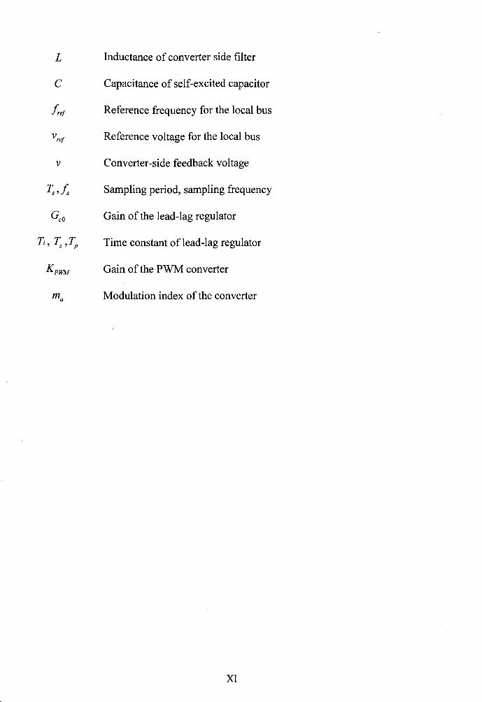
L Inductance of converter side filter
c Capacitance of self-excited capacitor
fref Reference frequency for the local bus
vref Reference voltage for the local bus
v Converter-side feedback voltage
T:,fs Sampling period, sampling frequency
Gco Gain of the lead-lag regulator
T;, I:,TP Time constant of lead -lag regulator
KPWM Gain of the PWM converter
ma Modulation index of the converter
XI

Chapter 1 Introduction
Currently the world's energy consumption is greatly dependent on exhaustible fossil fuel,
which is also main source contributing the green house gas and pollution to the environment. In
this perspective, utilization of renewable energy, such as wind and solar energy, has gained con
siderable momentum since the oil crises of the 1970s. Wind power, as one of the alternative en
ergy options, is gaining increasing significance throughout the world. Wind energy is non
depleting, site-dependent, non-polluting, becoming the most promising energy source for the fu
ture. Large and grid tired wind energy conversion system has been widely installed in many
countries, in the effort to minimize the dependence on fossil based non-renewable fuels [1].
Wind energy has experienced accelerated expansion in recent years and its global production is
predicted to grow from 60,000 MW in 2005 to 300,000 MW in 2015 [2].
1.1 Wind Energy Conversion System
A basic wind energy conversion system (WECS) consists of a wind turbine with tower,
gearbox, generator, power converter and control system, as shown in Figure 1-1[3]. There are
two types of wind turbines used in practice: vertical wind turbine and horizontal wind turbine
according to the rotating of the blades. Most modem wind turbines are horizontal type with two
or three blades due to higher efficiency and higher power capability.

Figure 1-1: Typical diagram of wind energy conversion systems
WECS can also be classified into two types of the systems according to its operation: con-
stant speed or variable speed operation systems. Fix speed WECS operate at a nearly fix speed
while variable speed system adjusts its rotor speed according to different wind speed. Generally
variable speed system extracts more wind energy (10-15%) than the fixed speed system.
A constant speed WECS usually contains a squirrel cage induction generator, as shown in Figure
1-2. Gearbox is necessary for the coupling of the low speed wind turbine and the high speed in
duction generator. SCR controlled starter between the generator and the grid aims at reducing the
inrush current during connection to the grid. In normal operation, induction generator absorbs
reactive power. Capacitor bank provides the required reactive power for generator. If enough ca
pacitor is provided, the generator can be self-excited, which is useful when grid is not available.
The speed of the generator varies little when the power changes. Thus the speed is almost con-
stant. Constant speed WECS is usually easier to built up and cost less than the variable speed
WECS. But because of the fixed speed, the overall energy conversion efficiency is not high.
Figure 1-2: Constant-speed wind energy conversion systems
2

Variable speed configurations allow the rotor to rotate at required speed by introducing
power electronic converters between the generator and the grid. Wind turbine system can operate
at its optimum tip-speed ratio[4]. Thus more energy can be converted into electricity. Double-fed
induction generators (DFIG), wound field synchronous generators and permanent magnet syn
chronous generators are three typical generators used in high power WECS. For medium and
small power wind turbines, permanent magnet generators and squirrel cage induction generators
are more often used because of their reliability and cost effectiveness. The typical configurations
ofvariable speed WECS are shown in Figure 1-3[5].
(a) Inductor generator with full power converter
(b) Doubly-fed induction generator with fractional power converter
Figure 1-3: Typical configurations of variable speed wind energy conversion systems
Power converters are used to control the power flow between the wind turbine and grid when
the variable frequency and variable voltage energy from generator is fed to the grid with fixed
frequency and voltage. Most modem power converters are forced commutated PWM converters
to provide a fixed voltage and frequency output with a high power capability. Both voltage
source voltage controlled converters and voltage source current controlled converters have been
3

applied in wind energy applications. For certain high power wind turbines, effective power flow
control can be achieved where real power and reactive power are independently controlled.
Most of the large wind energy conversion systems are grid connected. And many turbines are
installed in a utility level wind farm with several hundred MW installed capacity. The prediction
and power fluctuation are the main problem for the integration of wind farm to the grid. Many
research efforts have been to solve these problems.
WECS sometimes can be used in the standalone power system in remote area where grid
connection is not available. Hybrid system with battery, diesel generator and wind tur
bine/generator are connected together to provide a quality power to the load. The systems are
often used in the small community; the capacity varies from several kilo-watts to hundreds of
kilo-watt.
1.2 Stand-alone Wind Energy Conversion System
Many remote communities around the world cannot be physically or economically con
nected to an electric power grid. The electricity demand in these areas is conventionally supplied
by small isolated diesel plants. These have the advantage of being able to deliver the required
power whenever it is necessary. However, they also suffer from a number of drawbacks. Diesel
generator engines are inherently noisy and expensive to run, especially for consumers in rural
areas where fuel delivery costs may be high. In addition, small consumers always have a low
load factor; this in tum reduces the overall efficiency and increases percentage maintenance costs.
Considerable fuel savings can be achieved by integrating renewable sources such as wind and/or
solar energy with existing diesel plants.
However, many off-grid places are in regions of high wind energy potential. Wind energy is
one of the most important and promising forms of renewable energy sources. Its use is becoming
more and more popular nowadays. This is because the price of fossil fuels is continuously in
creasing and the wind energy is a clean and inexhaustible energy source. But due to great varia-
4
tion in wind speed which occurs from season to season, it can not be used as an autonomous
source of generation. Hence, it is necessary to explore possibilities of combining a wind genera-
tor with the diesel generator in order to reduce the running cost per kWh and to increase the reli-
ability of the power supply[6].
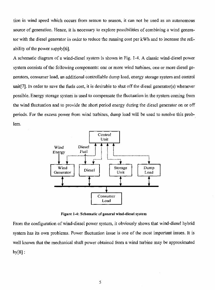
A schematic diagram of a wind-diesel system is shown in Fig. 1-4. A classic wind-diesel power
system consists of the following components: one or more wind turbines, one or more diesel ge-
nerators, consumer load, an additional controllable dump load, energy storage system and control
unit[7]. In order to save the fuels cost, it is desirable to shut off the diesel generator(s) whenever
possible. Energy storage system is used to compensate the fluctuation in the system coming from
the wind fluctuation and to provide the short period energy during the diesel generator on or off
periods. For the excess power from wind turbines, dump load will be used to resolve this prob-
lem.
Wind Diesel : Fuel j
r·----------- -------·
Wind Generator
Diesel
Control Unit
. . . . . . . . . : • .......................................................... :: ~--··-----i
Storage Unit
Consumer Load
Dump Load
Figure 1-4: Schematic of general wind-diesel system
From the configuration of wind-diesel power system, it obviously shows that wind-diesel hybrid
system has its own problems. Power fluctuation issue is one of the most important issues. It is
well known that the mechanical shaft power obtained from a wind turbine may be approximated
by[8] :
5

(1-1)
where pis the air density, C P (A, fJ) is the power coefficient, R is the blade radius, j1 is the
blade pitch angle, A is the tip speed ratio and Vis the effective wind speed respectively.
Equation ( 1-1) shows that small variations in the wind speed produce large changes in the
captured power. These power fluctuations transferred to the output by the conversion system,
including generator, power converter if existed, especially when the system is a fix speed system.
For variable speed systems, part of the power fluctuation is absorbed as kinetic energy in the tur-
bine. However, even for variable speed systems, power fluctuations can still be a serious prob-
lem if the generator is feeding a weak grid or a stand-alone load. For these applications, the wind
turbine is augmented by an additional source, usually a diesel generator. In such hybrid systems,
wind speed fluctuations not only produce fluctuations in the generator output voltage, but also an
unacceptable number of start/stop cycles of the diesel generator if a temporary energy buffer is
not available.
In [11-14], flywheel energy storage device is used as energy storage system to smooth the
fluctuations in the wind-diesel system when the energy storage system is needed. Papers [11, 12]
suggest that use vector control to control the induction machine to drive the flywheel system. [13]
also shows a new sensorless field oriented control method to drive the induction machine. Al-
most all the control methods are based on the front-end converter. There are other papers [15-17]
using battery bank or super-capacitor as the energy storage devices. The different kinds of en
ergy storage device have its own advantages and disadvantages. Battery is a cost effective solu
tion which is widely used in the energy storage system. But it has a high maintenance cost and
low cycle life. Super-capacitor is a new energy storage device with much higher life but the ca
pacity is low.
In [9, 10], sensorless control for double-fed induction generator in stand-alone system are
presented. For the Doubly-fed induction generator, sensorless operation is desirable because the
use of a position encoder has several drawbacks in term of robustness, cost, cabling and mainte-
6

nance. Most of the sensorless control methods are all based on the principle of rotor position ob
servers using the rotor current error. For DFIG, itself can regulate the output voltage and the fre
quency regardless of the load and rotational speed. Batteries, as the energy storage devices, are
integrated into the de link of back-to-back converter for the DFIG, which enhance the system
performance by expanding the operation range.
1.3 Motivation and Objective
Based on the configuration of the stand-alone system presented in the previous sections, the
typical system consists of wind turbine, diesel engine, energy storage system and control part. In
this project, the induction generator is used to be the wind turbine generator. For a small scale
wind-diesel wind power system, squirrel cage induction generator is a better choice when cost
and reliability are the first two considerations. As long as the energy storage devices are always
need, a fixed-speed self-excited induction generator has its own advantages including cost, ro
bustness and reliability can be used in the stand-alone system. The fluctuation in the power from
the wind can be smoothed by the energy storage system with an appropriate controller.
As presented in the former section, many researches have been done on doubly-fed induc
tion generator control. It usually uses a fractional size back-to-back converter to control the ac
tive power and reactive power to keep the constant voltage and frequency. And the controller
usually contains two control loops to regulate the voltage and frequency. For a doubly-fed gen
erator based system, the control of system voltage and frequency are very complicated since it is
coupled by the control of induction generator's speed and torque.
Most of the control strategies for power balance controlling in the stand-alone system con
tain two cascaded loops: voltage loop and frequency loop, which based on the assumption that
frequency loop is usually slower than the voltage loop. In these control systems, the dynamic re
sponse of grid voltage sometimes is not satisfied when the load is light.
7

In this thesis, the induction generator with self-excitation capacitor is directly connected to
the standalone power system, as shown in Fig.l-5. The energy storage system (ESS) is employed
to maintain the system frequency as well as voltage at collect bus. It supplies or absorbs the frac
tional power of the system, and keeps the system power flow balanced. When the wind energy is
not enough for a long period, the back-up generators including diesel generator should be turned
on to provide the rest of the energy. The renewable energy converters in the system are main
tained at highest efficiency with the employed ESS, which reduces the energy consumption from
diesel generators, reduces system operation cost as well as the greenhouse gas emission and pol-
lution to the environment.
Load
Energy Storage devices
Figure 1-5: Proposed wind energy conversion system
Therefore, the main objectives of the thesis are:
1. Design a suitable controller for converter, which smooth the power fluctuation of wind en-
ergy conversion system.
2. Develop mathematical models for the system with induction generator and energy storage
converter. This model will be used in the controller design.
3. Conduct variety of experiments to verify the performance of the developed control system.
1.4 Thesis Outline
This thesis is organized to provide the detailed information about the research work on
standalone wind energy conversion system with induction generator and energy storage devices
in five chapters.
8

This chapter, chapter 1 presents the background of wind energy conversion systems, includ
ing the configurations, operation and grid connection. Standalone power system with integrated
wind energy is introduced. Research motivation is discussed in this chapter.
Chapter 2 presents the development of mathematical model for each component in the stan
dalone system with wind turbine and energy storage devices. The model is developed in the d-q
reference frame. Finally the whole system model is developed.
Chapter 3 presents the direct voltage controller design for standalone WECS. Small signal
model of wind energy power system is developed; followed by theoretical analysis of the control
scheme with dump load and current protection. The diagram of controller scheme is discussed.
Chapter 4 shows all the simulation models for different components in Matlab/Simmulink.
The simulation results are also given in this chapter. Experimental results are provided to com
pare with simulation.
Chapter 5 presents the conclusions of the thesis, major contributions and future work are
discussed later.
All other relevant supporting materials are attached in appendices.
9

Chapter 2 WECS
Model Development for the Standalone
2.1 Introduction
The diagram of the proposed wind energy conversion system is shown in Fig. 2-1. The elec-
trical part consists of the induction generator with self-excitation capacitors, the energy storage
devices with power converter, consumer load and dump load.
L, RL vs
~~ em
L
Energy v Storage
devices
Figure 2-1: Proposed wind energy conversion system
In the system, self-excitation capacitors are needed to provide sufficient reactive power to
the induction generator, which reduce the reactive power consumption from the power converter.
It is assumed that the wind turbine is properly selected, which can provide most of the energy to
the load. Thus the power converter and energy storage devices only provide fractional power to
maintain the power balance between generator and load. In the system, the dump load will be
connected to absorb these extra powers from induction generator. The dump load can be repre
sented additional resistor. In the practical industry application, most of the energy storage de
vices usually can only store or supply limited power. So a back-up generator is essentially re-
10
quired if continuous power flow is required. In this thesis, energy storage devices are treated as
an ideal voltage source. Different characteristics of the batteries are not the main research focus.
Battery management is also not a consideration in this thesis.
Power fluctuation in the standalone system is one of the most common problems. Before
deriving a solution for the controller, it is imperative to produce a comprehensive mathematical
model of the whole electrical system that can be used in the controller design. The following sec
tions provide different part mathematical models and the whole system model is presented in the
last section.
2.2 Wind Turbine Characteristic
Generally, the wind turbine systems can be classified according to their aerodynamic con
figuration, transmission design and their operational speed range. Further classification can be
performed based on the power output, the generator types, grid connection, etc.
The aerodynamic configuration divides the wind turbines in two main categories: the hori
zontal axis wind turbine (HA WT) and vertical axis wind turbine (VA WT). Due to reasons of
mechanical resonance, efficiency and size more than 95 percent of the currently operating wind
turbine designs are HAWT. The choice of this configuration has one major disadvantage that the
main components of the energy conversion system such as generator, gearbox, pitch control me
chanism, the power converter and the grid-interface device, have to be located in the nacelle of
the turbine. This leads to the increased demands on the stability, strength and cost of the support
structure.
Regardless of the aerodynamic configuration of the wind turbine, its absolute maximum
power extraction efficiency is restricted by the Betz limit of 59.3 percent.
The mechanical power extracted from the wind is mainly governed by three quantities
namely, the area swept by rotor blades, the upstream wind velocity and rotor co-efficient.
11
(2-1)
Cp, the power coefficient of rotor, itself is a function of tip speed ratio and pitch angle. A
typical coefficient of the wind turbine is given at Oo pitch angle. The optimal Cp is only possi-
ble at certain speed ratio. Yet, it is not always possible to maintain zero blade pitch, because it
would create unwanted output fluctuations as well as greatly increase the electrical and mechani
cal load on the whole system when the wind is too strong. In order to partially cure this problem,
the pitch control mechanisms (or stall control) are installed to regulate the position of the blades
and maintain the highest possible power the system can deliver.
2.3 Induction Generator Model
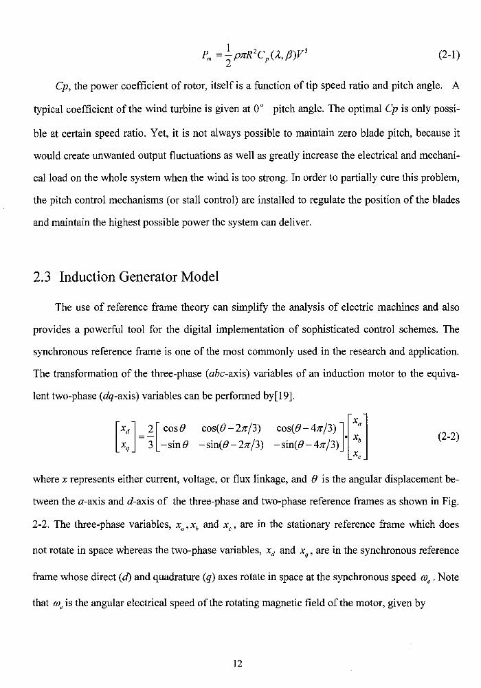
The use of reference frame theory can simplify the analysis of electric machines and also
provides a powerful tool for the digital implementation of sophisticated control schemes. The
synchronous reference frame is one of the most commonly used in the research and application.
The transformation of the three-phase (abc-axis) variables of an induction motor to the equiva-
lent two-phase ( dq-axis) variables can be performed by[ 19].
[xd] 2[ cosB cos(B-2;r/3) cos(B-4;r/3)] I xaj xq =3 -sinB -sin(B-2;r/3) -sin(B-4;r/3) 1:: (2-2)
where x represents either current, voltage, or flux linkage, and B is the angular displacement be
tween the a-axis and d-axis of the three-phase and two-phase reference frames as shown in Fig.
2-2. The three-phase variables, X0
, x6 and xc, are in the stationary reference frame which does
not rotate in space whereas the two-phase variables, xd and xq, are in the synchronous reference
frame whose direct (d) and quadrature (q) axes rotate in space at the synchronous speed me. Note
that me is the angular electrical speed of the rotating magnetic field of the motor, given by
12

q-ads
c-axis
Figure 2-2: Variables in three-phase (abc) stationary frame and two-phase (dq) synchronous frame
(2-3)
where fs is the frequency of the stator variables. The angle () can be found from
()(f) = ! OJe (t)df + ()0 (2-4)
In order to model the induction generator, the d-q equivalent circuit of induction machine is
obtained. Refer all the variables of rotor side to stator side, following equations can be obtained
by using Clark-Park transformation. The corresponding equivalent circuits are shown in Fig. 2-3.
(2-5)
(2-6)
Where:
Since the rotor rotates at speed OJr, the d-q axes rotate at the speed OJe - OJr referred to the
rotor frame. Therefore, the equations are:
13

0 R · dlfl dr ( ) vdr = =- ,ldr + --- OJe- OJ, lflqr
dt (2-7)
(2-8)
Where:
The rotor speed OJ, in equations (2-7) and (2-8) usually is treated as a constant during the
electrical transient. The electrical torque of the induction machine is given by
(2-9)
Where P is the number of the poles.
(a) d-axis equivalent circuit
(b) q-axis equivalent circuit
Figure 2-3: Induction generator equivalent circuits under synchronous reference frame
14

2.4 Inductive Load and Self-Excitation Capacitor Model
Capacitor is necessary in the standalone WECS. The capacitor can provide reactive power
to the induction generator. The equations (2-12) and (2-13) represent the relation between ca
pacitor currents and voltages in synchronous reference frame. For the load current and voltage, it
has
(2-10)
(2-11)
Through the Clark-Park transformation, the d-q synchronous reference frame equations can
be obtained:
(2-12)
(2-13)
Equations (2-14) shows the load voltages and currents in reference frame, assume of indue-
tive load.
(2-14)
2.5 Energy Storage System Model
The storage system consists of a bi-directional PWM voltage source based converter, grid
connection inductors and batteries. In this thesis, the battery's characteristic is neglected and
ideal voltage source Es is adopted. Since battery power management is another complex topic,
the research here focuses on the converter control to maintain a smooth power flow to the load.
The differential equations can be established for the energy storage system.
v(t) =dEs (2-15)
di(t) =_!_[v(t)-Ri(t)-v (t)] dt L s
(2-16)
15

In Eq. 2-15 and 2-16, d is the duty ratio, v(t) = [ va(t) vb(t) vc(t) r is converter output
phase VOltage. V,(t) = [ Vas(t) Vbs(t) Vcs(t)] T IS terminal (or bus) VOltage and
i(t) = [ ia (t) ib (t) ic (t)] r is converter side current.
+
Figure 2-4: Energy storage system circuit
The above equations can be transferred to selected dq reference frame by applying park-
clark transformation. Assume that the three-phase system is balanced three-phase three-wire sys-
tern, in which zero components can be removed. The two differential equations can be written in
Eq. (2-17) and (2-18), where ro is the rotating speed of reference frame.
(2-17)
(2-18)
2.6 Standalone WECS Model
16
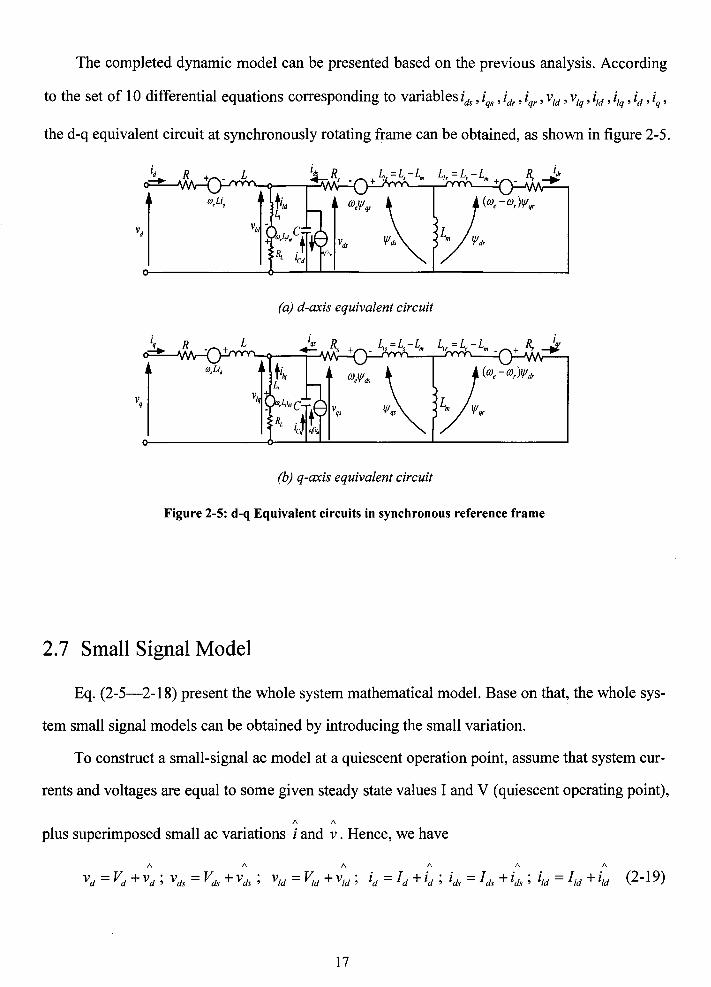
The completed dynamic model can be presented based on the previous analysis. According
to the set of 10 differential equations corresponding to variables id,, iqs, idr, iqr, v,d, v,q, i1d, i1q, id, iq,
the d-q equivalent circuit at synchronously rotating frame can be obtained, as shown in figure 2-5.
(a) d-axis equivalent circuit
(b) q-axis equivalent circuit
Figure 2-5: d-q Equivalent circuits in synchronous reference frame
2.7 Small Signal Model
Eq. (2-5-2-18) present the whole system mathematical model. Base on that, the whole sys
tem small signal models can be obtained by introducing the small variation.
To construct a small-signal ac model at a quiescent operation point, assume that system cur-
rents and voltages are equal to some given steady state values I and V (quiescent operating point),
1\ 1\
plus superimposed small ac variations i and v . Hence, we have
1\ 1\ 1\ 1\ 1\ 1\
vd=Vd+vd; vds=Vds+vd,; v,d=~d+v,d; id=ld+id; ids=lds+ids; i,d=l,d+i,d (2-19)
17

1\ 1\ 1\ 1\ 1\ 1\
vq = Vq +vq; vqs = ~' +vqs; v1q = v;q +v1q; iq = Iq +iq; iqs = Iq, +iqs; i1q = I,q +i1q (2-20)
A A
OJe = Qe + OJe; OJ, = n, +OJ, (2-21)
With the assumptions that the ac variations are small in magnitude compared to the steady
values, then the equations can be simplified. This is done by substituting Eqs. (2-20) and (2-21)
into Eqs. (2-5) and (2-6).
(2-23)
(2-24)
By cancelling the steady-state terms and neglecting high order ac terms in Eqs. (2-23) and
(2-24), the first-order ac terms on both side of the equations are left. Hence,
A
A A d IJ/ A A
R · 'f'ds ~ vds =- s 1ds + --- ue lflqs- OJe lf/qs
dt (2-25)
A
A A d 1/F A A
R . 'f'qs Q vqs =- slqs+--+ elflds+OJelflds
dt (2-26)
Where:
1\ 1\ 1\ 1\
lfl qs =-Lis iqs- Lm (iqr + iqs)
1\ 1\ 1\ 1\
lfl ds =-Lis ids- Lm (idr +ids)
Similarly, eqs. (2-25)- (2-26) can be derived.
(2-27)
(2-28)
18

Where:
1\ 1\ 1\ 1\
If! dr =-L,, idr- Lm (idr +ids)
1\ 1\ 1\ 1\
lflqr = -L,, iqr- Lm (iqr + iqs)
And similar procedures can be done on Eqs (2-130, (2-14), (2-16) to (2-18).
1\
di 1 1\ 1\ 1\ 1\ 1\
_d = -[vd- Rid- vd ] + Qe i +me I dt L s q q
1\
di 1 1\ 1\ 1\ 1\ 1\
_q = -[v - Riq- vqJ -ne id- OJe ld dt L q
(2-29)
(2-30)
(2-31)
(2-32)
(2-33)
(2-34)
The small signal equivalent circuit for the whole system can be given based on Eqs. (2-25)
- (2-34), as shown in Fig. 2-6.
(a) d-axis equivalent circuit
19

(b) q-axis equivalent circuit
Figure 2-6: Small signal model for d-q equivalent circuits in synchronous reference frame
2.8 Conclusions
In this chapter, the models of wind energy conversion system with induction generator and
energy storage system are presented based on the model for each component. System model is
developed to describe the dynamic behavior. Small signal model is derived based on the quies
cent operating point and linearization. The model will be used for the controller design in Chap
ter 3.
20

Chapter 3 Control of Standalone WECS
3.1 Introduction
Based on the small signal model in the last chapter, the system transfer function can be ob
tained. Traditional control method can be used in the regulator design. Direct voltage control
with current limit is developed for energy storage system to regulate the system voltage and fre
quency, and meanwhile, the real power and reactive power. In this research, compared with con
ventional power control with cascaded loops, the direct voltage control has faster dynamic per
formance with higher system bandwidth. The block diagram of the whole system is shown in
Figure 3-1. And the controller design will be discussed in the followed sections.
Figure 3-1: Control block diagram of the whole system
The stability analysis of the control system is based on the conventional method by using
bode plots of the control loop in s-domain. Once the transfer function of the open loop is derived,
the bode plots can be easily analyzed with the toolboxes in Matlab.
21
3.2 Direct Voltage Control
3.2.1 Voltage and Frequency Control
In Figure 3-1, the displacement angle for the synchronous reference frame is generated by a
given frequency, which is the reference frequency in the standalone WECS. In a standalone sys
tem, no synchronization is needed since the induction generator is indirectly controlled by the
power converter through adjusting the bus voltage. In the diagram, transformation block receives
the synchronous angle and transform the three phase local bus voltage into d-q reference frame.
Two lead-lag regulators are employed to directly regulate the d and q component voltages. The
target of the control system is to force the bus voltage follow the reference voltage through a
fixed frequency transformation. The frequency is indirectly controlled through the transforma-
tion block by the given frequency. Reference v; and v; are the desired bus voltage and the fixed
frequency is the desired system operating frequency. If the system outputs follow the references,
then active and reactive power balances are maintained.
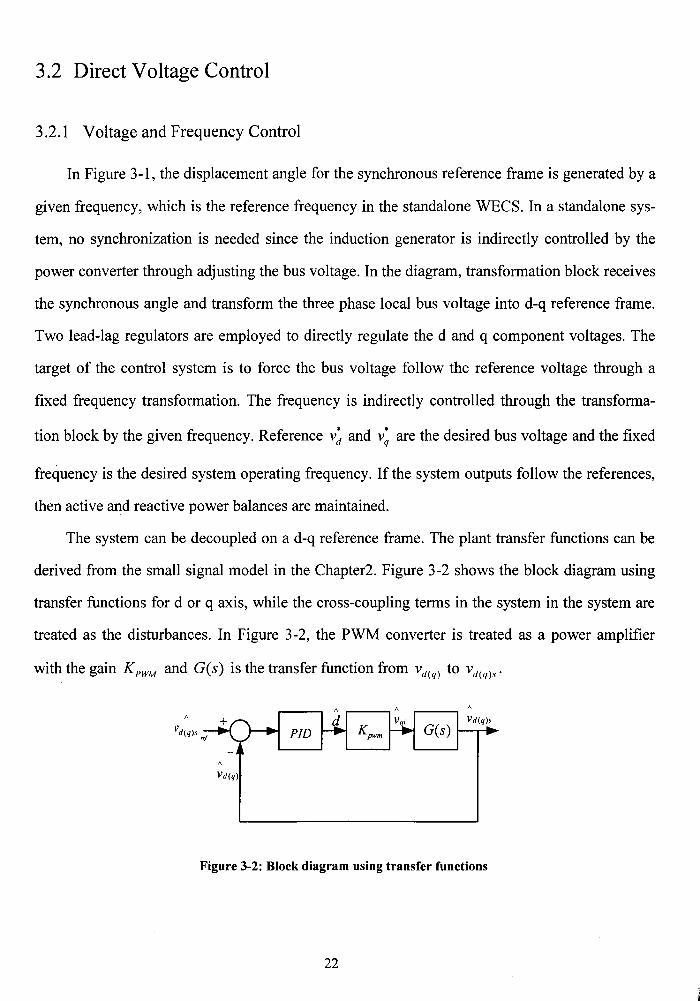
The system can be decoupled on a d-q reference frame. The plant transfer functions can be
derived from the small signal model in the Chapter2. Figure 3-2 shows the block diagram using
transfer functions for d or q axis, while the cross-coupling terms in the system in the system are
treated as the disturbances. In Figure 3-2, the PWM converter is treated as a power amplifier
with the gain KPWM and G(s) is the transfer function from vd(q) to vd(q)s.
PID Vd(q)s
G(s) 1---1~
Vd(q)
Figure 3-2: Block diagram using transfer functions
22

The controller for each axis uses a single loop to directly regulate the voltage. In this case,
compared with conventional power control with cascaded loops, it has a much faster dynamic
performance with even higher system bandwidth. Two lead-lag regulators are employed to regu
lated the d and q component voltages to obtain a higher phase margin and highest control band
width. The reference voltages can be arbitrary selected as long as the magnitude of the voltage is
desired voltage. Usually the d-component reference voltage v; is selected as the required local
bus voltage, while the q-component reference voltage v; is set to be zero. Space vector modula
tion (SVM) method is adapted to generate desired PWM gating signals.
It should be noted that the proposed system has no capability to protect the energy storage
system (EES) from overload since the output current is not sensed in the control system. In order
to protect the device from overload, several protection schemes have been developed. In this pa
per, dump load and current limit are employed together as the protection scheme. When the EES
side current exceeds the maximum operating current of switching devices, the proper gating sig
nal will be turned off to prevent the increase of current. The input power to EES is also detected,
and the dump load is switched on when the input power exceeds the maximum power capability
of the converter (or an energy storage device is applicable). The protection scheme with combi
nation of fast act current limit and slow act dump load (due to power detection) functions well
during overload. Other protections regarding over voltage, over temperature and devices short
through are similar to regular converter system.
3.2.2 Direct Voltage Controller Design
Shown in Figure 3-3, the system transfer function G(s) can be obtained from the small sig
nal model. The cross-coupling terms in the system are neglected since they are treated as the dis
turbances and compensated by either feed-forward or regulators.
23

Figure 3-3: System blocks model in S- domain
The local bus voltage is the system output. The converter voltage, which controlled by the
PWM signals is the system input. Then converter voltage to local bus voltage transfer func-
tionG(s) is shown in Eq. (3-1).
G(s) = vs (s) = Z2(s)Z3(s)Z4(s) (3_1) v(s) Z2(s)Z3(s)Z4(s) + Zt(s)[Z3(s)Z4(s) + Z2(s)Z3(s) + Z2(s)Z4(s)]
Where Z1 (s) is the transfer function of converter side filter. Z2 (s) and Z3 (s) are the trans-
fer functions of load and self-excitation capacitors. In the analysis, resistive load is assumed
since most of the consumer loads in the home are resistance loads, such as lighting, heating de-
vices and so on.
Z1(s) = sL
1 Z3 (s) =-
sC
(3-2)
(3-3)
(3-4)
Z4 (s) represents the induction generator in S domain. The magnetization inductance is
much bigger than the stator and rotor leakage inductances. So Lm can be neglected and the trans-
fer function can be simplified in Eq.(3-5).
Z4 (s) = (Rs + R,) + s(Ls + L,) (3-5)
Substitute the Eqs. (3-2)- (3-5) into Eq. (3-1), we have
G(s)= RL[(Rs+R,)+s(L5 +L,)] (RL + sL + s2 RLLCe)[(Rs + R,) + s(Ls + L,)] + sLRL
(3-6)
The bode plots of the uncompensated loop gain Tu(s) is shown in Figure 3-3, where
24

(3-7)
The parameters are selected based on the 2kW lab prototype system which is shown in Ta-
ble 3-1.
~
i
~ . ~
60
50
40
30
20
10
0
-10
-20
-30 0
-45
-90
-135
Table 3-1: Parameters of the Lab Prototype System
Load, RL 22Q
Converter filter inductance, L 10mH/20A
Excitation Capacitance, C 14lJLF
Stator Resistance, Rs 0.46Q
Rotor Resistance, R, 0.7Q
Stator Leakage Inductance, Ls 3.5mH
Rotor Leakage Inductance, L, 3.5mH
Converter Gain, K PWM 245
I I I I II II I I I I Ill I I I Ill -- -,--~-I -tll ItT---- --I-,-,-,-, T ,-,--- i - T -,- 11_1_1 It l- -,-I l TIll
I I I I I I Ill I 1 I I I II II I I I I I I Ill I I I I I Ill ---,- -,-1-illltT ·---,--I -,-,-,-,r,-,--- T -r -,-~,-,-,,,-- -~--,-ITT Itt
I I I I I Ill I I Ill I I I I I I 1 I I - - -,- I -,I 1 It I - - - ,- - I -, It-t- - - I - I - , ..... 1 I - -,- I I I
I __ 1_} ___ _ I I I I I Ill I I I I IIi I I I I I I
_I _ _!. _I _! _! !...._ll_ ___ 1 __ ~ _I _1_1 _1 _!_ 1_1 ___ _!_ _ _!_ _I_ I_ I_ 1_1
I I I I I I I I II I
___ 1 __ 1 _ _I_ _I_!_!_ !...._lj_ ___ I __ !___ _I_I_I_IJ_I_I ___ !_ __ I __ I_ !...._1_1_1!_1 ___ _J __ I_!____!_ _I_
I I I I I I Ill I I I I I II II I I I I I I Ill I I I I 1 II
___ 1 __ I _ __! _lj l_ Ul ___ 1 __ L _1_1_1_1_1_1_1 ___ l__.! _1_ !_1_1_1!_1 ___ J __ t__,l_ l _I_ LIJ
I I I I I I Ill I I I I I II II I I I I I I Ill I I I I Ill ___ I __ I _ _l ._) _j l Ll 1 ___ I __ L _I _1_1_1 1 1_1 ___ 1 _ l _I_ L I_ 1_1 Ll ___ _1 __ I_ L l L L I
I I I I Ill
I l I I Ill
I I Ill
"LL
I I I II II I I Ill
I I I I Ill I I I II II I I I I Ill -- -~- --1-11 T I1T--- -~-~-~-~-- ------ T -~-~~-~-111
I I I I Ill I I I I I I I Ill
I I I I Ill I I I II I I I I Ill
_! _I _I ..!_ ~I.!_ _____ ~ _I __ .!_ _ ..!_ _ I_ ~ I_ 1_1
I I I I Ill I I' I I I I I
I I I I Ill I I I Ill I I I I Ill
- - _i - _I - ~ ..!_ ..!_ I I I I I
I I I I I I Ill I I I I I Ill I I I I I Ill I I I I Ill ___ .1 __ I _ _l _I _j .l Ll1 ___ I __ L _, _l_l_llU ___ l _ l _I_ L 1_1_1 Ll ___ _j __ I_ L l l Ll
I I I I Ill I I I I Ill I I I I Ill
I I I Ill I I I I Ill I I Ill
Ill I I I Ill I I I I Ill
-180 lo-~-~-~-cl=-~-".Lo---±--"'-'L.±..H-±.c~~L._- .1- -1-1-1-1 ± j-J- -~-~±...cc..±.-=.J=-lcc..l=..l=L~~~"'--"'-"C=-L...L.L~~
10° 101 102 103 10"
Frequency (Hz)
Figure 3-4: Bode plots of uncompensated loop
25
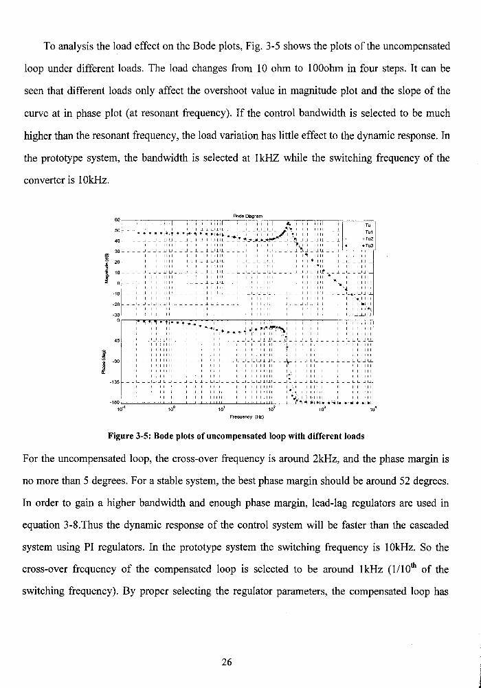
To analysis the load effect on the Bode plots, Fig. 3-5 shows the plots of the uncompensated
loop under different loads. The load changes from 10 ohm to 1 OOohm in four steps. It can be
seen that different loads only affect the overshoot value in magnitude plot and the slope of the
curve at in phase plot (at resonant frequency). If the control bandwidth is selected to be much
higher than the resonant frequency, the load variation has little effect to the dynamic response. In
the prototype system, the bandwidth is selected at 1kHZ while the switching frequency of the
converter is 1OkHz.
fiO -~,·-- I I I I I IIi ~--~~-~~~,~,~,~II r- I I I I I I rrl ~ I I I I ,-7~,-"P"'~~T~U'"-; 50 I I I I IIIII I I I I IIIII I I I llj_lll ~"".I II IIIII I
- -,-. ~ •r~fl'lf-.-.:-,.-~-~ ~ ;,; .•. ; ~::.__,- -,-,-,-, ,,-~J!'r-..~1-, ~ lrlrl- -~ ,~~~ 40 __ ,_ ..J _r_rJ uu __ J _ L 11 Lilli __ r!~.:-r..:.•-•l•tl"'"":_ _ -'--~i _r J UJil __ 1
I I I I I I I I I I I I I I I I II I I I 1 I I I II I ~. I I I I I II I •
Bode l:lagram
•Tu3 30 __ I __ I _1_1 J Ll Ll __ J _ l l l L_l_l_ll __ I __ I_ I_ 1_1 j_l_j_l ___ I _ l ~'J liJ lj_ __ j_ 'c=-ccCTT='
~ I I I I IIIII I I I I IIIII I I I I IIIII I I rflt,11111 I I I I II II
20 __ I _ _j _1_1 J Ll Ll __ J _ 1_ ..l l Ll.lll. __ L _I_ I_ U 1 1.1 I ___ I _ l _I J !! U lj_ __ _l _ I_ L Ll .J 1...1..
~ I I I I I II II I I I I I I Ill I I I I I I Ill I I I I I 1•11 I I I I I I II
t:t= 10 __ I_J_I_IJLILI __ J_LllLI_lll_ __ L_I_I_I_I_LI_ll ___ l_j__IJLIJI}' __ _l__I_LLI_ll_l_
I ~
l
I I I I I II II I I I I I I Ill I I I I I I Ill I I I I I I Ill • I I I I I I II
0 __ I_ .J _l_l_j L1 L1 __ J ~ L l l L1 .L I L __ L ~I~ I~ 1_1 .LUI~ ~ ~' ~ l _I J L U 1_1 ~ ---~-- I_ L L1 J U I I I I IIIII I I I I IIIII I I I I IIIII I I I I IIIII I,._ I I II II
-10 L-1- _j _l_l_j Ll Ll- - _j - L l l 1__1 .LI L - - L _1_1_ u .ll11_ - _I- 1 _j _j _L 1.1 11 - - .l - '-·'- Ll _j. 11_.1_. I I I I I I I I I I I I I I I I I I I I I I I I I I I I I I I I I I I I I I I~ .. I I I I
-20 - -I _ _j _I~' .J Ll Ll- - .J - L l 1 Ll .L I L - - L _I_ 1_1_1 .ll11_ - _I - l _j J L IJ l_l - - l -I_ L Lt4tl_li
I I I I IIIII I I I I IIIII I I I I IIIII I I I I IIIII I I I I 11,.1
-30 ' 0
-.1 l'I'TI~•·I•-..i-.1 I IIIII I I I 1111~ I I II IIIII
: : : : : : :: : : : ; ·~: ~: r •• :. ~ ·: ~ ~ :~-~~-~: : : : : : : :: I I I 1111
I I I I II II
I I I I II II
-45 I -: _: -: -: ~: ~: __ ~ _ !_ l l ~I_LI !_ __ :- -: _ :-:-: ~ :~: __ .~1 __ l -: ~ ; :-f :~ __ + _ :- ~ :-: ~ :~ I I I I IIIII I I I IIIII I I IIIII
I I I I IIIII I I I I IIIII I I I I IIIII i I I I IIIII I I I I II II
-90 __ I_ .J _1_1 .J U L1 __ .J _ _L 1 1 U _ll _L __ L _I_ I_ U .L111 ___ .,_ l .J .J l. 1.1 11 __ l_ _I_ L L1 J l__j_
I I I I IIIII I I I I IIIII I I I I IIIII 1' I I I IIIII I I I I II II
I I I IIIII I. I I I IIIII I I I I ill
I I I I I II II I I I I I I I II I I I I I I Ill ~~· I I I I I I II I I I I I I I I
-135 __ I_ ..J _l_l ..J Ll L1 __ _j _ L _l _l Ll l_ I L __ L _I_ I_ U j_ U I ___ J - J ..J _j L U l_l __ j_ _ I_ L L I ..1 I. .. .L
I I I I I I II I I I I II II II I I I I I I Ill I I I I I I I II I I I I I I II
I I I I I I I I I I I I I II I I I I I Ill I •, I t I I I I II I I I I I I
-1sol I---!::~~:~: ~.::--~-~11111 I I I IIIII ~·.·.·~,~IIIII
10-1 10° 101
102
103
Frequency (Hz)
Figure 3-5: Bode plots of uncompensated loop with different loads
For the uncompensated loop, the cross-over frequency is around 2kHz, and the phase margin is
no more than 5 degrees. For a stable system, the best phase margin should be around 52 degrees.
In order to gain a higher bandwidth and enough phase margin, lead-lag regulators are used in
equation 3-8.Thus the dynamic response of the control system will be faster than the cascaded
system using PI regulators. In the prototype system the switching frequency is 1OkHz. So the
cross-over frequency of the compensated loop is selected to be around 1kHz (1/lOth of the
switching frequency). By proper selecting the regulator parameters, the compensated loop has
26

around 52 degrees phase margin at 1kHz. The bode plots of compensated loop gain T(s) (Eq.3-9)
are shown in Figure 3-6.
G ( ) = G _1 +----"Tz_s 1 + I;s c S cO
1 + TPs I;s (3-8)
(3-9)
The parameters value of the lead-lag controller is shown in table 3-2, which are calculated
through traditional method.
Table 3-2: Parameters of lead-lag Controller
r: Tp I;
1 1 1
27!*340 2n*2900 2;r *100
Bode Oagram
Frequency (Hr.)
Syst.mT Rl•• Margin (deg): 49.e Delay MwgWl (sec): 0.000133 Atfre(J.Iency (Hr.): 1.03e+003 ao.ed Loop Stable? Y• ·-
10
): Bode plot of compensated loop gain
27
H:

3.3 Conclusions
In this chapter, a novel direct voltage control is proposed. Based on this analysis, the system
local bus voltage and frequency can be regulated by the two control loops for d-q reference
frame. But due to the non-sensed current, current protection scheme is employed in this control
system. Based on the developed system transfer function, the direct voltage controller can be de
signed based on the traditional lead-lag regulator with increased the system phase margin and
extended the system bandwidth. Thus reliability and dynamic performance are improved.
28

Chapter 4 Simulation and Experimental Results
4.1 Introduction
Both simulation models and experimental setup were built for the verification of the pro
posed wind energy conversion system with induction generator and energy storage. The whole
system model was created using Simulink/Matlab. In the simulation, the system consists of the
three major components: the wind power generation system with energy storage devices, the
controller for power converter and the load. The wind turbine drives the induction generator to
run at the based speed. In order to simulate the wind fluctuation, the wind speed is assumed to
have the random changing around the base speed time by time. And the controller is used to re
gulate the local bus voltage and frequency constant. The details will be presented in the follow-
ing sections.
As shown in Figure 4-1, the experimental set-up consists of a back to back converter, iso
lated transformer, a DC motor, an induction generator and a DSP-FPGA based digital controller.
The proposed system is based on the 2kW Lab Volt wound-rotor induction machine set.
208V ....----, L- type Filter
Gate ~ Drive {')
DSP+FPGA Board
r . -liieaT . 1
I Energy 1 ,.....____._----~._,
I Storage 1
I Device 1 i Function I '-r---r---r-'
i_ tjn!!_ _1
Figure 4-1: Block diagram of experimental set-up
The multipurpose back to back power converter was designed and built for several projects.
In this project, one side of the converter works as a PWM rectifier, which maintains the DC link
29

voltage constant. This part is functional as an ideal energy storage device. And the other side
works as an inverter to maintain the local bus voltage and frequency constant with direct voltage
control. The DC motor and induction generator are mechanically coupled together. The DC mo-
tor is operated as a prime mover to drive the induction generator in the super-synchronous speed-
mode. The Texas instruments TMS320F2812 DSP and Altera's Cyclone FPGA were employed
as the core of the digital controller. Some experimental variables, such as dq components voltage
and current, are captured form DSP internal memory since these variables are not directly avail
able on the oscilloscopes.
4.2 Simulation Model
The whole system consists of the three major components: the wind power generator with
energy storage, the controller for power converter and the load, as shown in Fig. 4-2.
Figure 4-2: System models of proposed WECS
The system parameters of the prototypes system is shown in Table 4-1. Same paramters are
used in the simulation.
30
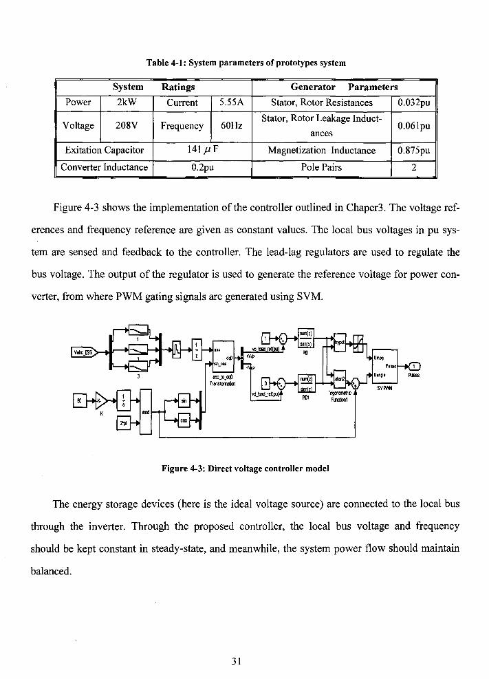
Table 4-1: System parameters of prototypes system
System Ratings Generator Parameters
Power 2kW Current 5.55A Stator, Rotor Resistances 0.032pu
Voltage 208V Frequency 60Hz Stator, Rotor Leakage Induct-
0.06lpu ances
Exitation Capacitor 14l,uF Magnetization Inductance 0.875pu
Converter Inductance 0.2pu Pole Pairs 2
Figure 4-3 shows the implementation of the controller outlined in Chaper3. The voltage ref
erences and frequency reference are given as constant values. The local bus voltages in pu sys
tem are sensed and feedback to the controller. The lead-lag regulators are used to regulate the
bus voltage. The output of the regulator is used to generate the reference voltage for power con
verter, from where PWM gating signals are generated using SVM.
Figure 4-3: Direct voltage controller model
The energy storage devices (here is the ideal voltage source) are connected to the local bus
through the inverter. Through the proposed controller, the local bus voltage and frequency
should be kept constant in steady-state, and meanwhile, the system power flow should maintain
balanced.
31

4.3 Simulation Results
4.3.1 Non-ESS Stand Alone Wind Power Generation System
When the WECS is connected to the load without the energy storage system, the local bus
voltage and frequency will have a large fluctuation due to the wind speed fluctuation. The system
configuration in simulation is shown in Figure 4-4. The wind turbine model use the standard
block provided with the Simulink' s Simpowersystem block set. The based wind speed is set to be
1 Om/s. A random source, whose range is from -1 to + 1, is used to simulate the fluctuation in the
wind. As shown in Fig. 4-5, the voltage and frequency have large fluctuations produced by wind
generator without ESS. Both are not constant. So the power quality is not acceptable.
Wind Turbine
Main Load
~==1---~A..,nchronousGenerator III Capacitor~
Figure 4-4: Wind power generation system without ESS
I ' ' j ' ' '
.j
0 4 5 6 7
(a) Single Phase Local Voltage (pu)
~V I i : J.!\'r,l ! N :~·~~\/~·······r·········rj·····~
10
0 1 2 3 4 5 6 7 8 9 10
(b) System Frequency (Hz) Time{s)
Figure 4-5: System voltage and frequency without ESS
32
4.3.2 Simulation Results with ESS
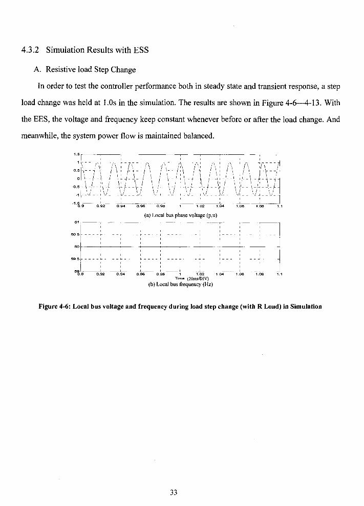
A. Resistive load Step Change
In order to test the controller performance both in steady state and transient response, a step
load change was held at l.Os in the simulation. The results are shown in Figure 4-6-4-13. With
the EES, the voltage and frequency keep constant whenever before or after the load change. And
meanwhile, the system power flow is maintained balanced.
1.5 ----,-~----,---,------,
I I
: fJJNlfNS/ 1AYV I
·~o~.9~2-~0~.~~-o~.oo=--~o.9~-~1~.o~2--~1~.~~-1~.o~6-~1.o~a~
(a) Local bus phase voltage (p.u)
60.5 - - - - r- - - - - t- - - - - t- - - - - t- - - - - -t - - - - -t - - - - -t - -
I I I I
1.1
sor--~--+--~--+---+--+---+--~--~--~
I I I I
59.5 - - - - 1- - - - - l- - - - - l- - - - - -+- - - - - -+- - - - - ..j. - - - - -l- - - - - -I - - - - -I - - - -
I I I I I I
5~_'::og---:::-o_-::-:92o------;;:o-'=.94:-----::o-'=.oo:::-----::oC::.9c::--B ---:-1----:;1-.~0~2 ---:1~.oco-4 ---=1~.o~s---,1~.o;;ca---;;1. 1 Time (20ms/D!V)
(b) Local bus frequency (Hz)
Figure 4-6: Local bus voltage and frequency during load step change (with R Load) in Simulation
33
I I I I I -- ·-~------~---~-----~---r:r-~"~-,---.----,---:------t
I I I I I I I I 0.8 ---- t---- -~-----I ---I-·-----~----- I---- I-----~----- r----
0.6 ----I------~----·- I---- I-----~----- r---- I-----~----- I----
I I I 0.4 -----;---- -~----- r- ·---- --t---- -~---- -r----- --t---- -~---- -r-----
I I 0. 2 ·- - - - -I- - - - - f- .. - - --+ - - - - --I- - - - - t- - - -· - --j - -· - -· - 1·- - - - - t- - - - -
I 1 I I
0 -----+-- ·-- -1---- ·- f----- --1-----1-----1----- --1---- -I----- 1-----
I I I I I
-0.2 _________l_. ·-- _ _____1_~- l __ _
0.9 0.92 0.94 0.96 0.98 1.02 1 04 1.06 1.08 1.1
(a) d-axis component of local bus voltage (p.u)
,------,-------T-~--,---,---,-,---,,---,---,---,----,
I I I I I I I I ---- 1---- -~-- - -- 1----- -i- - - -- -I---- I-----~----- I-
I I I I I I 0.8 - - - - I - - - - -~- - - - - I - - - - I - - - - -~- - - - - f - - - - I - - - - -~-- - - - - r - - - -
0.6- --- 1---- -~----- r----- ·1-- ·-- -~----- r---- 1---- -~----- r----I I I I
0.4----- -t---- -1----- r----- --t---- -~----- r----- --t---- -r----- t----
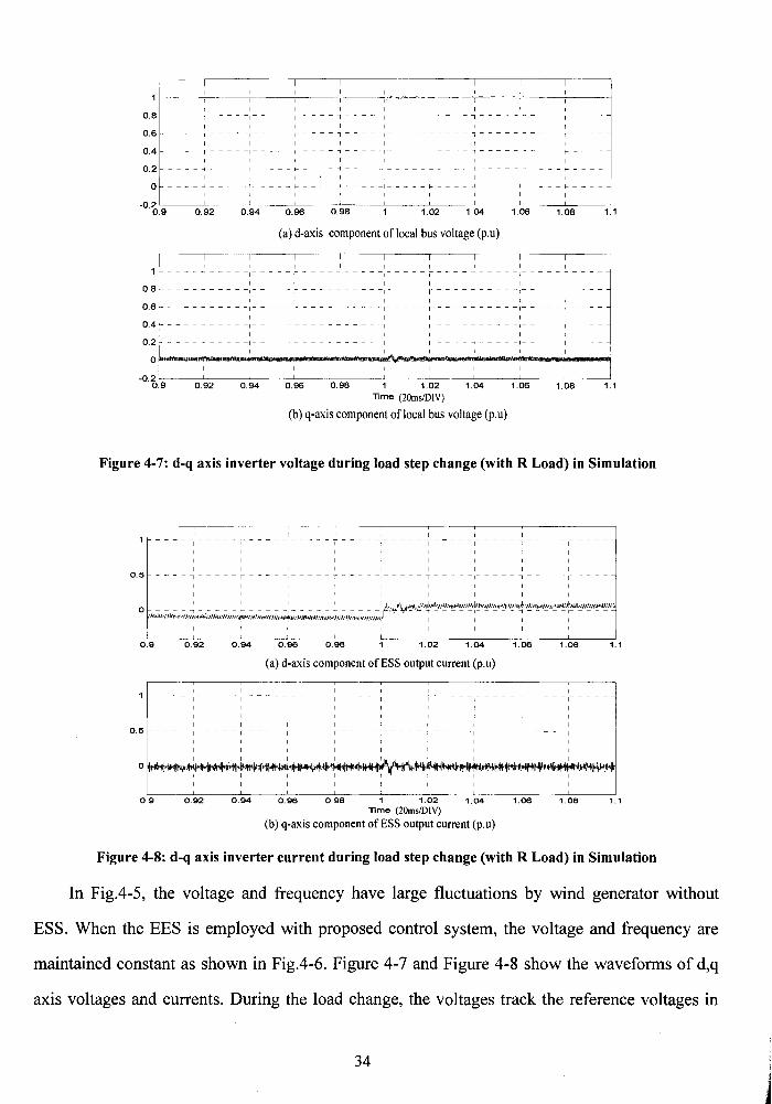
I 0.2- - - - -+ - - - - -I- - - - - f- --+ - - - . -1- - - - - t- - - -- - --+ -- - - - -I- - - - - t- - - - -
1 I
0~--~--~----~--------~--~~~------~--~--------~ -0.2L---~--~---L--~~---L-__ _L __ ~---~--_L--~
0.9 0.92 0.94 0.96 0.98 1 1.02 1.04 1.06 1.08 1.1 Time (20ms/D!V)
(b) q-axis component of local bus voltage (p.u)
Figure 4-7: d-q axis inverter voltage during load step change (with R Load) in Simulation
I I I I I I I I I - - - - -, - - - - - I - - - - -~ - - - - - I - - - - -,- - - - - I - - - - - ,- - - - - ' - - - - - 1- - - - -
I
0.5 --- -~----- f---- -~----- T---- -~---- -~-----~-----I-----~-----
I I I I I
0 ~~v~ J 1 - - - - -~- - - - - --t - - - - - r- - - - -
I
I I I
0.9 o."e-2=----=o-'=.9:-:4---,i~s---=-o.-'=9-=-8---t---1~.o=-=2=----c1-:.04~- 1.06 1.08
(a) d-axis component ofESS output current (p.u) ~---,---~~-
I I I I I I I I I - - - - -~ - - - - - I - - - - -~- - - - - I - - - - -~- - - - - I - - - - -~- - - - - I - - - - - 1- - - - -
I I 0.5 ----I----- r---- -~----- T---- -~----- T---- -,----- t---- -~-----
I I I
0.9 0.92 0.94 0.96 0.98 1 1.02 1.04 1.06 1.08 Time (20ms/DIV)
(b) q-axis component ofESS output current (p.u)
1.1
1.1
Figure 4-8: d-q axis inverter current during load step change (with R Load) in Simulation
In Fig.4-5, the voltage and frequency have large fluctuations by wind generator without
ESS. When the EES is employed with proposed control system, the voltage and frequency are
maintained constant as shown in Fig.4-6. Figure 4-7 and Figure 4-8 show the waveforms of d,q
axis voltages and currents. During the load change, the voltages track the reference voltages in
34

very well with a small transient. It also can be observed from the waveforms that the frequency
transient is less than ± O.lHz and voltage dip is less than 1%. There is no steady-state error in the
voltage and frequency due to the merits of synchronous frame and lead-lag regulators.
0.4 ,-------,-------.---,--,----,--------,---,.-----.------,-----,
0.2
-{).2
-{).4 'o----::-'=----=-':-.,----------:c"=----=:-::::----'------:-':c::----:-":-:---~--,-L-__j 0.9 0.92 0.94 0.96 0.96 1 1.02 1.04 1.06 1.06 1.1
(a) ESS output current (p.u)
- - - - j_ - - - - ..j._ - - - - -1 - - - - -1- - - - - - - - - - 1- - - - - >--- - - - - +- - - - - _J. - - - -
I I I I I I
I I I I I I ---- r---- I---- I-----~-----~-----~----- r---- T---- I----
7-----:~-~-:-------=-'::-.:------::~-~-~-- '.-:-------:-~-----c~--:J 0.9 0.92 0.94 0.96 0.96 1 1.02 1.04 1.06 1.06 1.1
(b) Generator side current (p. u)
:~ tV~A/\1\ cf\j\y: 1\-<1[\
1 I I I I I I -~ \ I v
-{),4 c
0.9 0.92 0.94 0.96 0.96 1 1.02 1.04 1.06 1.06 1.1 lime (20ms/DIV)
(c) Load side current (p.u)
Figure 4-9: Current waveforms during load step change (with R load) in simulation
Fig.4-9 shows the current waveforms from the generator, ESS and load. The ESS absorbs
the real power before l.Os and provides real power afterl.Os. EES also compensates the fluctua-
tion in the real power due to wind fluctuation at the same time. In the whole process, the power
flow in the system maintained balance all the time.
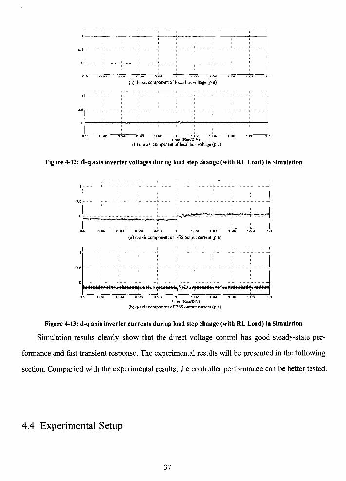
B. Inductive Load Step Change
Fig.4-10 to Fig.4-13 show the simulation results with RL-load change at l.Os. Fig.4-10
shows the local bus voltage and frequency. It has a similar response with the R load change.
There's no significant change both in voltage and frequency. Fig. 4-11 shows the current wave
forms with RL-load in simulation. The generator and EES together provide the real power. The
reactive power is compensated from ESS. Fig. 4-12 and Fig.4-13 shows the d-q axis voltage and
current simulation waveforms during load change. The d/q component voltages have very small
dip. The d/q current components reflected the real power and reactive power from the EES re
spectively.
35

-1.5 0.9
I
--~0~.9~4----0~.~96~--~0~.9~8~--~-----1~.0~2~--~1~.04~---:1·~----1~.~08~---71.1
(a) Local bus phase voltage (p.u)
' ---------------00.5 ____ L ____ L _________ L __ _ I I I 1 I 1
60~----.------,------,-----,------,-----.------,------,-----,----~
59.5 --- -~---- -r---- -j---- -j---- -1-----1---- -j---- -1---- -j----
I I I I I
59~--~~~--~~--~~--~~~--~----~~--~~--,-~~--~=---~ 0.9 0.92 0.94 0.96 0.98 1.02 1.04 1.06 1.08 1.1
Time (20msiDIV)
(b) Local bus frequency (Hz)
Figure 4-10: Voltage and frequency during load step change (with RL load) in simulation
I I I I I I I - - - - I - - - - I - - - - I - - - - -I- - - - -~- - - - - 1- - - - - I - - - - T - - - - I - - - -
0.9 0.92 0.94 0.96 0.98 1 1.02 1.04 1.06 1.08 1.1
(a) ESS output current (p.u)
-0.5
0.92 0.94 0.96 0.98 1 1.02 1.04
(b) Generator side current (p.u)
Figure 4-11: Currents waveforms during load step change (with RL load) in simulation
36
I
I I I I I I I I I 0.5 - - - - 1- - - - - 1- - - - -~- - - - -1- - - - I - - - - 'l - - - - T - - - - T - - - - I - - - -
I I I I I 0 ____ I _____ I _____ I _____ I _____ I ____ _j ____ _l_ ____ _L ____ L ___ _
I I I I I I I I I
I I I
0.9 0.92 0.94 0.96 0.98 1.02 1.04 1.06 1.08 1.1
(a) d-axis component of local bus voltage (p.u)
1 - - - - 1- - - - -1- - - - -1- - - - -1- - - - -I - - - - -I - - - - j_ - - - - ..l- - - - - 1- - - - -I I I I I I I I I
I I
I I I I I I I I I 0.5 - - - - 1- - - - - 1- - - - -1- - - - -1 - - - - I - - - - I - - - - T - - - - T - - - - r - - - -
0~---------------.----------~~------------~----._--~ 0.9 0.92 0.94 0.96 0.98 1 1.02 1.04 1.06 1.08 1.1
Time (20ms/DIV) (b) q-axis component of local bus voltage (p.u)
Figure 4-12: d-q axis inverter voltages during load step change (with RL Load) in Simulation
1 ----1-----1-----1-----1-----1-----1-----1-----1-----1-----
l I I I I I I I I
I I
0.5 - - - - 1- - - - - I- - - - - 1- - - - - 1- - - - - 1- - - - - I- - - - - 1- - - - - I- - - - - 1- - - - -
I I I I I I
0 ----f-----f-------1-----f----- ~-
1
I
0.9 0.92 0.94 0.96 0.98 1.02 1.04 1.06 1.08 1.1
(a) d-axis component ofEES output current (p.u)
1 ----~----~----~----~----~----~----~----~----~----1 I I I
0.5 - - - - I- - - - - 1-- - - - - 1- - - - - 1- - - - - 1- - - - - L- - - - - 1- - - - - L- - - - - 1- - - - -
I I
I
I I I I I I I I I
0 - - - -I- - - - - 1-- - - - - 1- - - - - 1-- - - - -I- { ~- -I- - - - - 1- - - - - 1-- - - - - 1- - - - -
rr 'f "" T '1
0.9 0.92 0.94 0.96 0.98 1 1.02 1.04 1.06 1.08 1.1 Time (20ms/DIV)
(b) q-axis component ofESS output current (p.u)
Figure 4-13: d-q axis inverter currents during load step change (with RL Load) in Simulation
Simulation results clearly show that the direct voltage control has good steady-state per-
fonnance and fast transient response. The experimental results will be presented in the following
section. Companied with the experimental results, the controller performance can be better tested.
4.4 Experimental Setup
37

The whole system experimental setup is shown in Fig.4-14, where part "A" is the DC motor,
and part "B" is the induction generator. The DC motor and induction generator are mechanically
coupled together. The DC motor is operated as a prime mover to drive the induction generator in
the super-synchronous speed mode. Part "C" is the self-excition capacitor. The output of the in
duction generator is connected to the local bus, and only provides the real power to the load. The
energy storage system is simulated by a back-to-hack converter, which is part "D" in Figure 4-14.
One side of the converter works as a PWM rectifier, which maintains the DC link voltage con
stant. This part is functional as an ideal energy storage device. The power fluctuation is buffed
through the grid. And the other side works as an inverter to maintain the local bus voltage and
frequency constant with direct voltage control, and meanwhile, keep the system power hal-
anced .. The DC link voltage is rated at 400V, and the Local bus voltage was rated at 208V/5.55A.
Part "F" is the DSP-FPGA controller board. And part "E" is the filter inductor for PWM con-
verter.
Figure 4-14: Experimental setup
(A: DC motor; B: Induction generator; C: Self-excited capacitor; D: Converter; E: Line indcutors; F: DSP-FPGA controller board)
The controller design developed in Chapter3 was implemented using the DSP-FPGA plat-
form as shown in Fig.4-15. The controller hardware used in this experiment consisted of the ana-
logue signal conditioning board, DSP ("A"), FPGA, interface circuit ("B")and a LED display
("C").
38

Figure 4-15: DSP controller board
(A: DSP chip; B: Interface circuit; C: LED display)
The controller algorithm from chapter3 was transferred into the DSP using C programming
language. The complete code for the controller is given in Appendix D.
The system voltages and currents are sensed and fed to the conditioning circuit, which fed
the signals to the AID converter. The results of AID converter are fetched by the DSP and used
as the feedback signals. The final output signals of the DSP board are the switch signals for the
PWM converter. The role of the FPGA in this experiment is to provide the phase information for
the grid-side rectifier and to provide protection for the power converter in case of abnormal con
ditions. For this purposes the over-voltage, over-current and over-temperature protection circuits
are interfaced directly with the FPGA to provide instantaneous protection of the power devices.
In this system, the switching frequency is selected at 4.5 kHz. Higher switching frequency obvi
ously would be better in the performance, but switching loss should be considered in the practi
cal design.
The operational sequence of the controller is developed as following. First the gird side
converter is energized. Once it is activated, the converter boosts the DC voltage to the required
400V. At this time the local bus side converter is turned on and works with constant V/f control
strategy to drive the induction generator speeding up until it goes into steady state. The large
starting current in the induction machine is avoided in the V /F control. And then, adjust the DC
39
motor input voltage to increase the input power until the rotating speed beyonds the synchronous
speed. Now, the induction machine is operating in generator mode. The load then is connected to
the local bus. And the controller starts to maintain the local bus voltage and frequency constant.
The turn-off sequence for the converter is the opposite procedure of the start-up. In practical, the
wind turbine speeds up the generator. The generator builds up the voltage with self-excitation
capacitor. When the voltage reaches the desired level, the generator is brought to the local bus
and ESS is started to maintain the local bus voltage and current. During the connection, synchro
nization is needed between ESS and generator. But in the experimental setup the synchronization
is not necessary since the machine is started through the converter directly.
4. 5 Experimental Results and Analysis
The performance of the direct voltage control was evaluated on the prototype system at sev
eralload conditions. The load step change is necessary. Through the load step change, the tran
sient procedures are captured using the oscilloscopes through the voltage and current sensors.
For different kind ofloads, the local bus voltage and frequency are kept constant with direct vol
tage control. And the system power flow is maintained balanced with the ESS.
4.5.1 Resistive Load Test
Resistive load is connected on the local bus. When the generator starts up and goes into
steady state, a three phase resistive load is connected to the system local bus. The resistor value
is 120 n. The steady state waveforms of the voltage and current at different sides are shown in
Fig. 4-16.
40
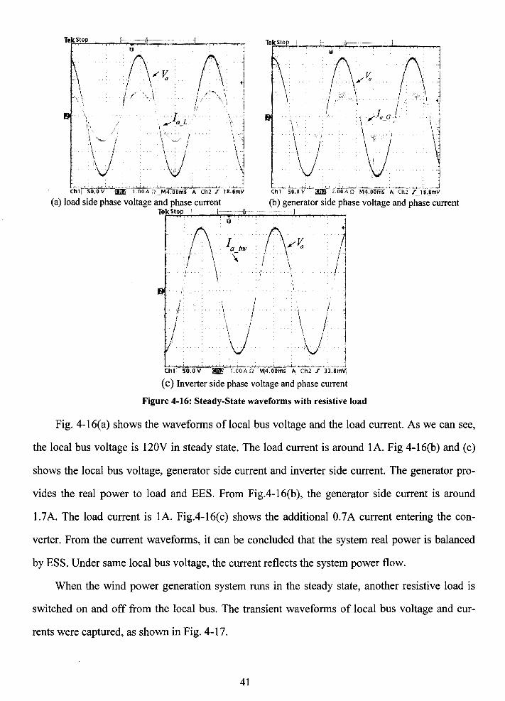
ThkSto ThkStop
1.1(\•··. ~ p··· • j I (a .. ·. ····. 1 I '· . . ~'- t·
I I . ] i · •.. \. '· '\ /. · a_G :· · •\· ·., -.....-.a L 1 .
\,;, ij \···; \J···' ~ v ~ v .... j . ' . I
Chl''"'"so:OV""~tii!tl~o·'MI4.to-niS''A®f '1&.6;;,~ clii~"-so.ov"'ooE .·{;t;,'\~[f"i>llo"tnit',;;ch:i':ffs~ilm~ (a) load side phase voltage and phase current (b) generator side phase voltage and phase current
TekSto ~---- -l'r--------------1
;
(\ /\
·' ,!, .
. ,.
! J
j f! ' ~ . .. l
i l \ / \ I -l
I \ I \ ;·. j
' .. 'J v 1 . . . . . . . . 1
clll['itrv·...,i!frr&O'AI~:cM~76olilt'·~ 'ctit:t':ti':smv (c) Inverter side phase voltage and phase current
Figure 4-16: Steady-State waveforms with resistive load
Fig. 4-16(a) shows the waveforms of local bus voltage and the load current. As we can see,
the local bus voltage is 120V in steady state. The load current is around IA. Fig 4-16(b) and (c)
shows the local bus voltage, generator side current and inverter side current. The generator pro-
vi des the real power to load and EES. From Fig.4-16(b ), the generator side current is around
1.7A. The load current is IA. Fig.4-16(c) shows the additional 0.7A current entering the con-
verter. From the current waveforms, it can be concluded that the system real power is balanced
by ESS. Under same local bus voltage, the current reflects the system power flow.
When the wind power generation system runs in the steady state, another resistive load is
switched on and off from the local bus. The transient waveforms of local bus voltage and cur-
rents were captured, as shown in Fig. 4-17.
41

Ch1 1
Figure 4-17: Transient waveforms of local bus voltage and load current during load step change
Fig. 4-17 shows the waveforms of local bus voltage and load current during the load change.
After the additional resistor is switched on, the load current increases twice. From Fig.4-17, it
can be seen that the local bus voltage has very small transient and thus a very small frequency
change.
Fig 4-18 shows the waveforms of generator side current, inverter side current and load side
current in the transient. It should be noted that the fluctuation in the generator current came from
the oscillation of motor/generator set caused by load change. EES quickly compensates this os-
cillation and maintain the bus voltage/frequency constant. It also shows in Fig.4-18(b) that the
ESS changes the power directional from absorbing excess real power to supplying the additional
real power to the load.
42

ThkSto
I I
~ f', ('\1 I i 1 I 1 _1 ·I · \ ,. I v \) \
I 1V I_
I I I I I I I
-~ :". f.. r, \ . (\ /\
:;
' ' v v J
I .,
.... _ ..... 'i.....-~·"-' ..i. ....... ,~,J •.. ,J .. _.,_._ '· .•. i ..... '"""' ! •• i.,.. .... .,. , .... t-±, .... J.. .... .~.-., ,.,_L..;. .. ..:..' ....... L""- ,, . ...._ ch1[~2:ooA a·-. z:!fo A 11 M:iHJ:(fms· "'. Chl r 3.o4 A
i l I I·
(a) Load phase current and generator side phase current (b) Load phase current and inverter side phase current
Figure 4-18: Transient waveforms of generator and converter currents during load step change (with R Load)
Voltage and current dq components waveforms of converter side are also captured from the
DSP memory during the load change, as shown in Fig. 4-19. The reference voltage for vd and vq
are 1.0 pu and 0 pu respectively. The voltage dq components trace the references very well. The
current dq components are often referred to the real power and reactive power respectively. As it
can be seen, id changes from negative to positive, indicating the power flow change for ESS.
From the waveforms, it can be concluded that the control system has fast dynamic response dur-
ing transient. And the steady-state error is almost zero because of the lead-lag regulators.
06
0.6 0.6
0.4 0.4
02 .,
.02 .0.2 20ms 20ms
(a) d-axis voltage component (Vb=169.68V) (b) q-axis voltage component (Vb=l69.68V)
43

~~---~--I--·· -t - -- T --I-- 1-- -1--
I I I I I I
I I - -~-- -~- ----,- -~-- T- -,-- -~-- -~--
I I I I I I
I I 1 l - - -1 -- T - - I - ,- - -~- -
I I I I I I I - -~- - -~ - - I - - I - - -- - - 1- - - 1- - ·- 1- -
I
(a) d-axis current component (h=7.85A)
1 - - 1- - -I- - -I- - -1- - ...., - -I - - + - - + - - 1- - -
I
0.8 - - :- - - 1- - -1- - -1- - 4 - - ---t - - T - - T - - t- - -
I I I I I
' - 1- - -I- - -~- - -1 - -- ·1 - - I - - I - ~ T - - r - -I I I
I I I I O.<l - - 1- - -~- - -~·- - -~- - -1 - - l - - 1 - - T - - I - -
I I I
' .0.2 __ I ___ I ________ ___! __ J __ l __ 1 __ L __
I I I I I
I I .4).<1 __ ____L_L___j _ _j__J____J_ _ _j___J
(b) q-axis current component (h=7.85A)
Figure 4-19: d-q axis Inverter side current during load step change (with R Load)
4.5.2 Inductive Load Test
The system performance is also verified by connecting the inductive load. A three-phase
120Q resistor bank and a 0.31H inductor bank are connected to the bus in parallel. With RL
load, the controller still maintains the local bus voltage and frequency constant by providing the
reactive power to the load. The steady state waveforms are shown in Fig. 4-20.
TekStoJ>
I
'"'.,. J;; I ,, i \
j I .,
-·1
1
/\ I \ /· \
\
1 l 1
I ~
I . \j .. ; .. ~--r ·'· L,. ,+ .~--.~J ............. C,.· "'; ~o"'-"--' -""""""'·""'··•.) :. ...... ..-. .f.-•• c• ~'"'" .........,_.,. _,.__,.,_,_ • ..,,;~-~, •. :.-'--1.-.l....cj
Chl 50.0 V Iii!. 2.00A It Mr!.OOms f>1 Ch2 f 2S.2mV
(a) load phase voltage and phase current (b) generator phase voltage and phase current
44

TekSto
(\/v· ,d._,. I \
I .. \ \
\ ; v \
\ \ \ I
I I I I ·v
A I I I I I ,
(c) Inverter side phase voltage and phase current
Figure 4-20: Steady-State voltage and current waveforms with RL load
Fig.4-20(a) shows the waveforms of local bus voltage and load current. Because of the RL
load, the load current and voltage have about 45 degree phase displacement. Fig.4-20(b) and (c)
show the waveforms of local bus voltage, generator side current and inverter side current. The
generator only provides the real power to the load. So the current and voltage are almost in phase.
The inverter absorbs the extra real in the system and provides the reactive power to the load. So
the inverter side current lags the voltage at about 45 degree. From the Fig.4-20, it reflects the
system power flow always maintains balance with the EES in the steady state.
Load step change is also carried in the RL load condition. When the whole system runs into
steady state, an additional load (120ohm) is switched on and off. The transient waveforms are
shown in Fig. 4-21 and Fig.4-22.
The local bus voltage and load current transient waveforms are given in Fig.4-21. It is simi-
lar to the waveforms with pure resistive load, and the local bus voltage has a very small transient.
Fig. 4-22 shows the transient waveforms of the load current, generator side current and inverter
side current.
45

Figure 4-21: Transient waveforms of local bus voltage and load current during load step change (with RL load)
Tekstop
(\ {' /1; I i: :·I ..
'I ·,I l f v I I I I I I I I I
....... • .. +·····..i , .. : .. > , ;I; :,. •...•.. , .... ..! •• ~~-·" ......... : .......... ,.J ...... i .... __. ..... ,... , , , , .i .... ~ ..... ..~ .. ,.-<-.. •··-·····: Chl 2.00" n tilE 2. oo i\ P M;2o.oms " Chl r 3.40"
TekStop
IT
I ~ ,': f': ,\ .11· /II ,' \ !' . ~ / 1
i I I
1'v V :, I I I I
I I I I I
//"-""
'v
.. ~.i ......•. o.i .~ • d. • ··"··•~-'""· • • .•..• • .... ~ --~'"-'·'··1.~'·' •""-•~·•~ ·' Chi i.oo An tilE 2.0oAZi. M2ii:oms A Chl f 3.40 A
(a) Load phase current and generator side phase current (b) Load phase current and inverter side phase current
Figure 4-22: Transient waveforms of currents of generator and inverter during load step change (with RL load)
Inverter side voltage and current dq components waveforms are also given in Fig. 4-23. The
voltage dq components are very similar to the pure resistive load. During the load change, vd has
a very small dip and then went back to the reference value quickly. Current waveforms are also
similar to the resistive load condition. Since the load change is only on resistance, id has the
same waveform as resistive load and iq maintains at -0.2 pu.
46

0.8
0.6
0.4
0.2
... 20ms'
.0.41'----'---'--_._._ _ _,__-'-----'----'------'---'---'
(a) d-axis voltage component (Vb=169.68V)
0.8
0.6
0.4
.0.4 c___. _ ___.. _ __L_ _ __,__-'----'--_j__-'"--"-__j
(c) d-axis current component (Jb=7.85A)
0.8
0.6
0.4
0.2
-0.2
20ms
.0.41L_---"-~---'---'--~-.L-.-"---'---'--_j
0.6
0.4
02
.0.6
(b) q-axis voltage component (Vb=169.68V)
20m ..-
.... L____.. _ _..._ _ _:,_ _ __.__...__.____. _ _... _ __,_ _ _.J
(d) q-axis current component (h=7.85A)
Figure 4-23: d-q axis Inverter side current and voltage during step load change (with RL Load)
1 __ j_ __ j_ __ j_ __ j_ __ j_ __ J.. __ _j_ __ J_ __ _J_ __
I I I I I I
0.8 __ j_ __ j_ __ j_ __ j_ __ j_ __ j_ __ J._ __ J_ __ J_ __
I I I
0.8 __ j_ __ j_ __ j_ __ j_ __ j_ __ .L __ .L __ j_ __ J_ __
I I I I I
0.4 __ L __ j_ __ L __ L __ j_ __ .L __ l_ __ _l __ .i __
I I I
0.2 - - L - - L - - L - - J.... - - L - - J.. - - _J_ __ J. __ J_ __
I I I I I 1, .. ._···~.1"""··""\~.r'f· .......... .
0 / .. \~"'-.1~'.;"\.-::{,,;::_;:.,_, I I I I I I I I I
-0.2 __ L __ j_ __ L __ L __ j_ __ .L __ J._ __ _l __ _l __
I
.0.4'-----'----'--_J ----'--L---'---'---L-._L__
(a) d-axis current component (h=7.85A)
'··~~-~-~____,-----,-----,----~-~
I
- -,- - -,- - -,- - ..., - - 1 - - T - - r - - r - -,- -I I
I I I I I o.a - - ,_ - -1- - -~ - - 4 - - -t - - -t - - r - - r- - - t- -
I I
o.a - -1- - -1- - -1 - - ---1 - - -+ - - T - - r - - r- - -1- -
I I I I I I I I I
I I 0.4 --I-- -I-- -1-- ---1---+- - +- - f--- 1- --I--
I I I I
0.2 - -I- - -I- - -1- - -I - - -+ - - .j.- - - 1- - - 1--- - -I- -
I I I I I I I I
I
0 - - 1- - -I- - -1- - _J - - -+ - - -1- - - 1- - - 1- - -I- -
I I I 1-........ /"'1'1'"
-0.2 --1---1---1-- -J- _ J. __ 1. __ L __ L- -1--
I I
(b) q-axis current component (h=7.85A)
Figure 4-24: d-q axis Inverter current during step load change with compensation (with R-L Load)
It should be noted that current dq components waveforms contain an ac component at fundamen-
tal frequency both in R load and R-L load situations. It is verified that the inverter side current
has a very small DC component. There are several reasons including non-symmetrical voltage
output, sensor de calibration and temperature drifting of the analog conditioning circuits. The last
47
two problems can be compensated through DSP using carefully calibrated circuit and de bias
compensation. But the unsymmetrical devices can not be avoided. The small DC voltage will
cause large DC current in the system due to small resistance. This is the drawback of the pro
posed control system, which has no capability to direct regulate the current. So a simple DC
compensation scheme is necessary in order to avoid the large DC current. The dq component
current waveforms after compensation is are shown in Figure 4-24.
4.6 Conclusions
The model for standalone WECS with induction generator and energy storage system is
constructed in the Simlink/Matlab software. The whole system with direct voltage control is veri
fied in simulation and experiment. Different load conditions and load changes are carried in this
project to verify the effectiveness of the controller. From the simulation and experimental results,
it can be seen that the directly voltage control can achieve desired steady state performance with
fast dynamic response.
48
Chapter 5 Conclusions
5.1 Conclusions
From the simulation and experimental results obtained in this thesis, several conclusions
can be drawn regarding the design of the directly voltage controller for the standalone wind en-
ergy conversion system with induction generator and energy storage system.
The dynamic mathematical model for the whole system is developed. Small signal model is
derived based on the dynamic model. The small signal model provides the basis for the controller
design. A lead-lag regulator based controller is developed to regulated the local bus voltage con
stant in synchronous reference frame. The reference frequency and voltages are selected at the
desired values. The transformer functions for d-q axis are developed. The regulator parameters is
calculated through the traditional design using phase margin and system bandwidth. lead-lag
regulators successfully improve system bandwidth while maintain high phase margin. Thus fast
dynamic response and small overshoot/undershoot can be expected. The system stability is also
improved.
The control scheme developed for the direct control of the system local bus voltage and fre
quency in the WECS has been tested using the simulation model and experimental setup. The
control system successfully maintains the system voltage and frequency constant under different
load condition and power fluctuation. The power flow in the system maintains balanced by the
power converter and ESS. The transient waveforms shown in the experimental results, corre
sponding with the simulation results, verify the expected response from controller design.
Overall, this research work has shown that the energy storage system with direct voltage
control can be effectively used in the stand-alone WECS. Though this kind of control scheme has
49 PROPERTY OF
RYERSON UN1Vf8S1TY UBRARY

its own drawbacks such as no capability of current protection, simple scheme can be used to
overcome the problems of overload protection as well as the de current. In this thesis, the em
ployment of squirrel cage induction generator gives benefit for reducing the manufacturing and
maintainance cost. The system reliability can also be improved compared to DFIG or permanent
magnetic machines. Only fractional capacity power converter is required in this configuration,
which further reduce the system cost.
5.2 Major Contributions
One of the main contributions of this work is the design of the direct voltage control for the
stand-alone WECS with induction generator and ESS. The control scheme shown in Figure 3-1
provides a novel control method compared with conventional cascaded control method. It di
rectly regulated the local bus voltage and frequency, and maintained the power flow balance in
the system. It has a faster dynamic performance and higher stability.
The configuration using induction generator is another contribution of this research work.
Because its own advantages, such as reliable, low cost, low maintenance, this configuration has
better cost per kW. The development of the small signal model is very useful for the controller
design. The model accurately represents of the system behaviour around the quiescent operating
point.
5.3 Further Research Works
In order to accommodate the system variations and improve the control system performance,
the following research work should be done in the further.
1) Overload test should be done in the experimental conditions. The drawback of the direct
voltage control is capability of current control. Current protection scheme should be improved if
necessary.
50

2) Multiple generators operation should be investigated in the future research. Sometimes
there are more than one wind turbine generators are connected to the local bus. The system mod
el will become complicated and the control of ESS will be difficult.
3) The characteristics of the different energy storage devices should be considered. In this
thesis, the energy storage device is assumed as an ideal source. In practice, the characteristic of
the energy storage device needs to be considered and optimized power management should be
implemented to increase the battery life.
51

References
[1] M.A. Elhadidy and S.M. Shaahid, "Role ofhybrid (wind+diesel) power systems in
meeting commercial loads", IEEE Transaction on Renewable Energy, vol. 29 pp. 109-
118,2004.
[2] L. Wei, G. Joos, and C. Abbey, "Wind Power Impact on System Frequency Deviation
and an ESS based Power Filtering Algorithm Solution," Conference record of Power Sys
tems Conference and Exposition, 2006. PSCE '06. 2006 IEEE PES, 2006.
[3] J. M. Carrasco, E. Galvan, R. Portillo, L.G. Franquelo and J. T. Bialasiewicz. "Power
Electronics Systems for the Grid integration of Wind Turbine," Conference record of IE
CON 2006- 32"d Annal Conference, 2006.
[4] J. Marques, H. Pinheiro, H. A Griindling, J. R. Pinheiro, and H. L. Hey, "A Survey on
Variable-Speed Wind Turbine System," conference record of CE. 7° Congresso Brasileiro
Eletronica Potencia - COBEP'03, Fortaleza, Brazil, 2003.
[5] Chen, Z and Spooner, E., "Grid interface options for variable-speed, permanent-magnet
generators," Electric Power Applications, lEE Proceedings, Vol145, pp 273-283, July
1998.
[6] A. S. Kini, AS. Kini, and R. Y. Udaykumar, "Modelling And Performance Analysis of
A Wind/Diesel Hybrid Power System," conference record oflndustry Applications, 2006.
41st lAS Annual Meeting.
[7] R. Sebastian, M. Castro, E. Sancristobal, F. A Yeves, J. A. Peire, and J. A Quesada,
"Approaching hybrid wind-diesel systems and controller area network," Conference re
cord of IECON 02, 2002. -[8] W. E. Leithead, "Dependence of performance of variable speed wind turbines on the tur-
bulence, dynamics and control," Generation, Transmission and Distribution, vol. 137, pp.
403-413, 1990.
52

[9] R. Cardenas, R. Pena, J. Proboste, G. A. Asher, and J. A. Clare, "MRAS observer for
sensorless control of standalone doubly fed induction generators," IEEE Transaction on
Energy Conversion, vol. 20, pp. 710-718,2005.
[10] R. Cardenas, R. Pena, J. Proboste, G. A. Asher, and J. A. Clare, "Sensorless control of a
doubly- fed induction generator for stand alone operation," Conference record of Power
Electronics Specialists Conference, 2004. PESC 04. 2004 IEEE 35th Annual, 2004.
[11] R. Cardenas, R. Pena, G. Asher, and J. A. Clare, "Control strategies for energy recovery
from a flywheel using a vector controlled induction machine," Conference record of
Power Electronics Specialists Conference, 2000. PESC 00. 2000 IEEE 31st Annual, 2000.
[12] R. Cardenas, R. Pena, G. Asher, and J. A. Clare, "Control strategies for enhanced power
smoothing in wind energy systems using a flywheel driven by a vector-controlled induc
tion machine,", IEEE Transactions on Industrial Electronics, vol. 48, pp. 625-635, 2001.
[13] R. Cardenas, R. Pena, G. M. Asher, J. A. Clare, and R. A. Blasco-Gimenez, "Control
strategies for power smoothing using a flywheel driven by a sensorless vector-controlled
induction machine operating in a wide speed range," IEEE Transactions on Industrial
Electronics, vol. 51, pp. 603-614, 2004.
[14] R. Cardenas, R. Pena, M. Perez, J. A. Clare, G. A. Asher, and P. A. Wheeler, "Power
Smoothing Using a Flywheel Driven by a Switched Reluctance Machine,", IEEE Trans
actions on Industrial Electronics, vol. 53, pp. 1086-1093, 2006.
[15] J. Yan, K. Oti, N. Yamamura, and M.A. I. M. Ishida, "A Study on Electric Power
Smoothing System for Lead-acid Battery of Stand-alone Natural Energy Power System
Using EDLC," Conference record of Power Conversion Conference- Nagoya, 2007.
PCC '07, 2007.
[16] A. Rufer and P. Barrade, "A supercapacitor-based energy-storage system for elevators
with soft commutated interface," IEEE Transactions on Industry Applications, vol. 38, pp.
1151-1159, 2002.
[17] Z. Jie, Z. Buhan, M. Chengxiong, and A. Y. W. Yunling Wang, "Use of Battery Energy
Storage System to Improve the Power Quality and Stability of Wind Farms," Conference
record of Power System Technology, 2006. PowerCon 2006. International Conference on,
2006.
53

[18] T. Tudorache, L. Melcescu, and S. V. Paturca, "Finite Element Analysis of Self-Excited
Induction Generator for Isolated Small Power Wind Turbines," Conference record of
Clean Electrical Power, 2007. ICCEP '07. International Conference on, 2007.
[19] Bin Wu, High-Power Converters and AC Drives, John Wiley & IEEE Press, 2006.
54
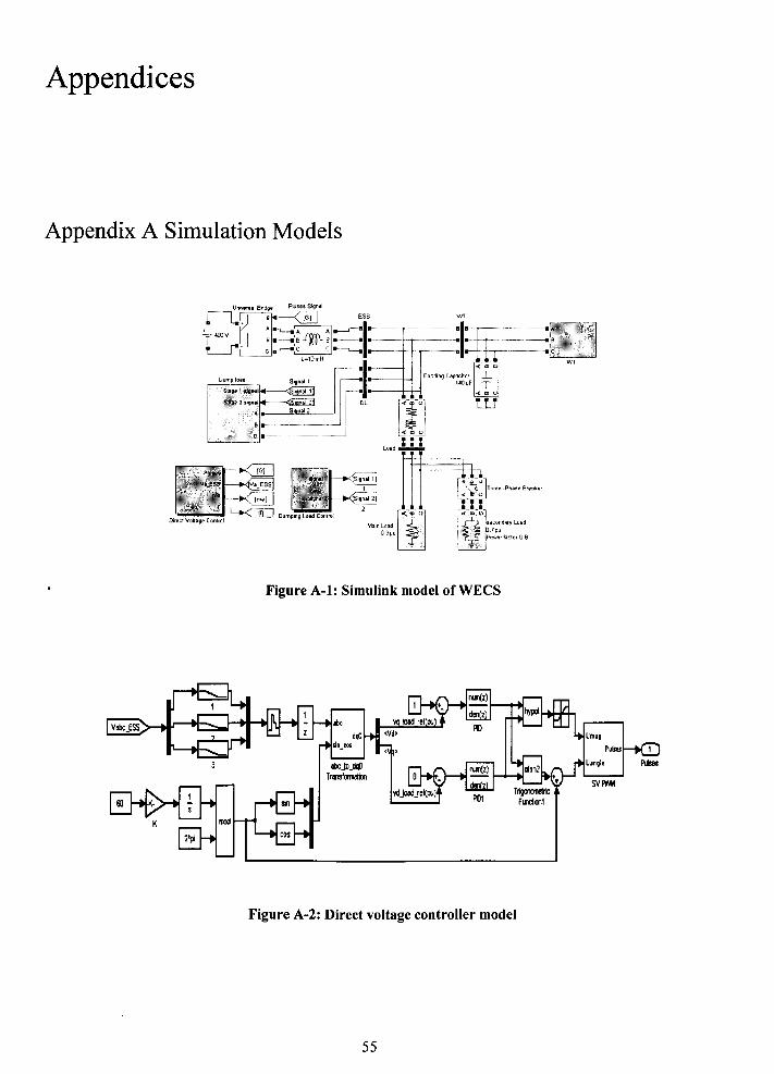
Appendices
Appendix A Simulation Models
Figure A-1: Simulink model ofWECS
Figure A-2: Direct voltage controller model
55

Appendix B System Parameters
Table B-1 Parameters of DC Motor
Operating Condition Motor
Power 2kW
Armature Voltage 120V
Shunt Voltage 120V
Armature Current 23 A
Shunt Current 0.81A
Speed 1800 rpm
Armature Inductance SmH
Armature Resistance 20
Table B-2: System Parameters of Prototypes System
System Ratings Generator Parameters
Power 2kW Current 5.55A Stator, Rotor Resistances 0.032pu
Voltage 208V Frequency 60Hz Stator, Rotor Leakage Induct-
0.061pu ances
Excitation Capacitor 141,uF Magnetization Inductance 0.875pu
Converter Inductance 0.2pu Pole Pairs 2
56

Appendix C Code for Bode Plots
M-file for bode plots of compensated and uncompensated loops
clear all; RL=22;Rs=0.46;Rr=0.70;Lls=0.0035;Llr=0.0035;Li=l0e-3; RL1=10;RL2=40;RL3=100; C=l.41e-4; Kpwrn=245; Rl=Rs+Rr;Ll=Lls+Llr; s=tf('s'); G=(RL*(Rl+s*Ll)/(RL+Rl+s*Ll+s*C*(RL*(Rl+s*Ll))) )/(s*Li+(RL*(Rl+s*Ll)/(RL+Rl+s *Ll+s*C*(RL*(Rl+s*Ll))) )); Tu=G*Kpwrn; Gc0=0.077; Tz=l/2/pi/340; Tp=l/2/pi/2900; Ti=l/(2*pi*l00); Time constant of LEAD-LAG Gc=GcO*(((l+Tz*s)/(l+Tp*s)))*(l+l/Ti/s); ~LEAD-LAG controller T=GcO*Kpwrn*Gc; 6open loop gain with compensat<:Jr bodeplot(Tu,T);
57

Appendix D DSP Program Code
DSP Program Code
/*************************************/ /*File Name: wecs.c *I /************************************/
#include "DSP28lx Device.h" Headerfile Include File #include "DSP28lx_Examples.h" Examples Include File #include "FPGA csr.h" #include "Display.h" #include <stdio.h> #include "IQmathLib.h"
II Useful Definitions #define ADC usDELA Y 8000 #define ADC usDELA Y2 40
3.1415926 1.732051 0.577350269
II DSP28lx
II DSP28lx
#define PI #definesqrt3 #define sqrt13 #define Sw _ freq 8997 .11/sampling frequency
#define AVE SAMPLE 8 //AVE SAMPLE=2AAVE SHFT - -#define AVE SHFT 3 #define AVE SAMPLE DC 16 - -//AVE SAMPLE DC=2AAVE SHFT DC - - - -#define AVE SHFT DC 4 - -
#define w DC 1000.0//cut-offfrequency(rad/s) of low-pass filter for DC voltage
#defmeXL inductance
0.016//0.016//Line to Converter
#define sen_posi 0//current sensor position, O:converter side, 1 :grid side
0.5 40.0//for DC voltage control loop
0.04 30.0//for current control loop
0.0796
#define Kp_Udc #define Ki Udc #define Kp _I #define Ki I #define Kp _ E #define Ki E #defme Kpp _ E #define Kii E #define Kdd E
0.005//for loacal voltage control loop 4.74
3.735 0.0058
58
#define K PLL close loop
778700.0//gain for motor angle
#pragma DATA_ SECTION(graph _data,"graph _data"); #pragma DATA_SECTION(graph_data1,"graph_data1 "); #pragma DATA_SECTION(graph_data2,"graph_data2"); #pragma DATA_ SECTI ON(graph _ data3, "graph_ data3 "); #pragma DATA_SECTION(graph_data4,"graph_data4"); #pragma DATA_SECTION(graph_data5,"graph_data5"); #pragma DATA_ SECTION(graph _ data6, "graph_ data6");
//#pragma DATA_ SECTION(wind _profile, "wind _profile");
*******************************/ /* VARIABLE DECLARATION *I /*********************************************
/* ADC */ Uint16 Sample_chO[AVE_SAMPLE], Sample_ch1 [AVE_SAMPLE],
Sample_ch2[AVE_SAMPLE], Sample_ch3[A VE_SAMPLE],
Sample_ch4[AVE_SAMPLE], Sample_ch5[AVE_SAMPLE_DC],
Sample_ch6[AVE_SAMPLE_DC], Sample_ ch7[ AVE_ SAMPLE],
Sample_ ch8[ AVE_ SAMPLE_ DC], Sample_ch9[AVE_SAMPLE],
Sample_chlO[AVE_SAMPLE], Sample_ch11[AVE_SAMPLE],
Sample_ch12[AVE_SAMPLE], Sample_chl3[AVE_SAMPLE],
Sample_chl4[AVE_SAMPLE], Sample_chl5[AVE_SAMPLE];
Uintl6 ConversionCount=O; Uintl6 ConversionCountl =0; int32 AD_BIASO, AD_BIASI, AD_BIAS2, AD_BIAS3,
AD_BIAS4, AD_BIAS5, AD_BIAS6, AD_BIAS7, AD_BIAS8, AD_BIAS9, AD_BIASIO, AD_BIASII, AD_BIAS12, AD_BIAS13, AD_BIAS14,
AD_BIAS15;
int32 lal, Ic1, Ia2, Ic2; //Uq18 format)
!* for testing*/ Uint32 watch =0; Uint16 watch1 =0; Uint16 watch2 = 0; Uint16 watch3 = 0; Uint16 Testswitch =0;
/*PLL */ Uintl6 Theta_con, Theta_err; //phase and error info in counter format Uint16 nmax,f; Uint32 Theta_pu; //line voltage angle in per unit value _iq28 Theta_line; //line voltage angle in radian value (0-2pi) _iq28 Theta _phase,angle _offset; //phase voltage angle in radian value _iq28 cos_theta, sin_theta;
/*======VSR variables======== */ float Udc_ref=400; II DC voltage reference _iq18 Vab, Vbc, Yea,
Ia, lb, lc, Vdc_P,Vdc_N;
_iq18 Va, Vb, Vc; _iq18 V _alpha, V _beta; _iq18 v _d, v _q;
/*Inner loop current control*/ _iql8 I_alpha, I_beta; _iq18 I_d,I_d_ref, I_d_err,I_d_errl, upper limit_ ld,lowwerlimit_ Id; _iq18 I_q,I_q_ref, I_q_err,I_q_errl;
_iql8 V _d_O, V _q_O; _iq18 I_d_inl, I_d_in2, I_d_out, I_d_outl, I_d_out2; _iql8 I_q_in1, I_q_in2, I_q_out, I_q_outl, I_q_out2; _iq28 kp_I, ki_I; //PI controller
/*Outer loop DC voltage control*/ _iq 18 V de _ref,V de, V dcO, V de_ L, V de_ LO, Vdc_err,Vdc_err1; _iq28 kp_dc, ki_dc; //PI controller
/*=========VSI variables========* I float Eq_ref=O; _iq18 Eab, Ebc, Eca,Ed_ref,EabO,VabO,
Iu, Iv, Iw; _iq 18 Tu, Tw;
_iq 18 Ea, Eb, Ec; _iql8 E_alpha, E_beta; _iq18 luvw_alpha, Iuvw_beta; _iq18 E_d, E_q,Ed_O, Eq_O;
59
_iq18 I_E_d, I_E_q; _iq18 V _d_L,V _q_L;
_iq18 Ed_err, Eq_err, erro_d, erro_q,Ed_errO, Eq_errO, Ed_err1, Eq_errl, Eq_D, Ed_D,Eq_D1,
Ed_D1, Ed_O, Eq_O,Ed_1, Eq_1;
_iq28 kp_E, ki_E, kpp_E,kii_E,kdd_E; II LEAD-LAG controller
/*Low-pass filter*/ _iq28 LPFa_DC,LPFb_DC;
/* SVPWM*/ Uintl6 Ts=16672;//PWM period in counter value Uintl6 Tl,T2,TO,Tc=O; int 16 section_ number; _iq28 Theta,Thetal,Theta_sec; _iq18 Mmag,Mmag1;
/*Generator position and speed up*/ _iq18 Speed_n; _iq28 Theta_INV; Uint16 Angle_CNT,Angle_CNTO,Speed_CNT; Uint16 Angle_index=O; Uint32 f_counter; Uintl6 count_f, tL, F;
/*Key input*/ int16 key_value,key_value1, key_monitor, key_ monitor 1 ,key 1 ;
/* Display* I Uint 16 display_ counter,display _counter 1;
/*Control flags*/ Uint16 MODE, Ill :Rec 2:Inverter
CONT ACTOR, /*For VSR:O-open, 1-close*/ CONTACTOR1, /*For VSI:O-open, 1-close*/
FAULT, /*0-no fault 1- fault detected*/ PLL, /*0-PLL not locked 1-locked*/ Fault_info_A, /*Result of fault detection from
left (A) side*/ Fault_info_B, /*Result offault detection from left (B)
side*/ Initial_ over, //"0-not over, 1- over"/
SCREEN; /*0-system status screenO 1-status screen 1 */ Uint16 Res_flag=O; Uintl6 test_number=O;
Uintl6 test_flagl=O;

Uint16 Ready=O;
Uintl6 T_CNTO=O; Uintl6 T_CNTl=O; Uintl6 T_CNT2=0;
/*Graph of waveform*/ intl6 graph_data[9000];//Vab int16 graph_datai [9000];//I_d_ref inti6 graph_data2[9000];//V _d inti6 graph_data3[9000];//V _q intl6 graph_data4[9000];//I_q intl6 graph_data5[9000];/!Vdc int I6 graph_ data6 [9000] ;//Theta _phase
Uinti6 indexO=O; Uintl6 graph_index=O; U int 16 graph_ index I =0; Uintl6 graph_index2=0; Uintl6 graph _index_ flag=O; Uintl6 data_shift_times=O; inti6 data_shift_timesi=O;
!*************************************! /*FUNCTION DECLARATION *I /*************************************/
interrupt void adc _ isr( void); interrupt void pdpinta_isr(void); interrupt void t3cint_isr(void); I /interrupt void EVB _ CAPINT 4 _ ISR( void); //interrupt void EVB _ CAPINT5 _ISR(void); //interrupt void ti ufint_isr(void);
void Protection_PLL (void); void get_ theta( void); void get_ frequency (void); void get_adc_ V(void); void abc_dq_transforrnation(void); void speed_up(void); void VSR _Reguiation(void); void VSI_Regulation(void); void SVPWM_ VSR(void); void SVPWM_ VSI(void); void Enable_Rec(void); void Disable_Rec(void); void Enable_Inv(void); void Disable_Inv(void); void Key_input(void); void Close_ Relay( void); void Close_ Relay 1 (void); void Open_ Relay( void); void Open_ Relay I (void); void AD_ bias 16( void); void Delay_mili_second (int delay); void get_speed(void);
60
void Init_ variable( void); void InitGpio(void); void InitXintfClocks( void); void InitPeripherals(void); void InitEV A( void); void InitEVB(void); void InitAdc(void); void init_fpga(void); void Buffer _rotating(int16 buffer[9000],Uintl6 shift_ times);
/*************************************/ /* NAME: main() */ /* RETURNS: void */ /*************************************/
void main( void) { II Step 1. Initialize System Control: II PLL(PLLCR=OxA), WatchDog( disable), enable Peripheral Clocks
InitSysCtrl();
II Step 2. Initialize the Xintf clocks InitXintfClocks();
II Step 3. Initalize GPIO: InitGpio();
II Step 4. Clear all interrupts and initialize PIE vector table:
DINT; II Disable CPU interrupts InitPieCtrl(); II Initialize the PIE control registers to
their default state. II The default state is all PIE interrupts
disabled and flags I I are cleared.
IER = OxOOOO; II Disable CPU interrupts IFR = OxOOOO; II Clear all CPU interrupt flags
InitPieVectTable(); //Initialize the PIE vector table
II Interrupts used are re-mapped to ISR functions EALLOW; PieVectTable.PDPINTA = &pdpinta_isr; PieVectTable.ADCINT = &adc_isr; PieVectTable.T3CINT = &t3cint_isr; Pie VectTable.CAPINT 4=&EVB _ CAPINT4 _ ISR; Pie VectTable.CAPINT5=&EVB _ CAPINT5 _ ISR; //PieVectTable.TlUFINT = &tlufint_isr; EDIS;
II Step 5. Initialize all the Device Peripherals: InitPeripherals();

II Step 6. User specific code, enable interrupts: PieCtrlRegs.PIEIERI.bit.INTxl = 1; //Enable
PDPINTA PieCtr1Regs.PIEIERI.bit.INTx6 = 1; //Enable
ADCINT in the PIE: Group I interrupt 6 PieCtriRegs.PIEIER4.bit.INTx5 = I; II Enable t3cint in
the PIE: Group 4 interrupt 5 PieCtriRegs.PIEIER5.bit.INTx5 = 1; II Enable
CAPINT4 in the PIE: Group 5 interrupt 5 PieCtriRegs.PIEIER5.bit.INTx6 = 1; II Enable
CAPINT5 in the PIE: Group 5 interrupt 6 //PieCtr1Regs.PIEIER2.bit.INTx6 = 1; //Enable tlufint
in the PIE: Group 2 interrupt 6
IER i= M_INTI; II Enable CPU INTI: IER i= M_INT4; II Enable CPU INT4: IER i= M_INT5; II Enable CPU INT5:
EINT; II Enable Global interrupt INTM ERTM; II Enable Global realtime interrupt DBGM
Clear_ LED(); AD_bias16(); Manu_ display(); AdcRegs.ADCTRL2.bit.INT_ENA_SEQl = 1; //
enable SEQl interrupt (every EOS)
II Step 7. Infinite loop while( I) {
if (FAULT == O)Key _input (); display_ counter++;
if( display_ counter==20000) { display_ counter! ++;display_ counter=O;
} if (display _counter I ==30) {
//Text_ LCD_ display(); I !key I= 1 ;//for test LED_ display(); display_ counter! =0; display_ counter=O; }
} } /*End Main* I
/***************************************/ !* NAME: adc_isr() RETURNS: void DESCRIPTION: Interrupt for ADC results revieval *I /****************************************/
interrupt void adc_isr(void)
61
{
Sample_ chO[ConversionCount ]=( (AdcRegs.ADCRESU LT0>>4) );
Sample_ chI [ConversionCount]=((AdcRegs.ADCRESU LT1>>4) );
Sample_ ch2[ConversionCount ]=( (AdcRegs.ADCRESU LT2»4) );
Sample_ ch3 [ ConversionCount ]=((AdcRegs.ADCRESU LT3»4) );
Sample_ ch4[ConversionCount ]=( (AdcRegs.ADCRESU LT4»4) );
Sample_ ch7[ConversionCount ]=( (AdcRegs.ADCRESU LT7»4) );
Sample_ ch9[ConversionCount ]=( (AdcRegs.ADCRESU LT9»4) );
Sample_ ch 1 O[ConversionCount ]=( (AdcRegs.ADCRESU LT10>>4) );
Sample_ ch 11 [ConversionCount ]=( (AdcRegs.ADCRESU LT11»4) );
II Sample_ ch 12[ConversionCount]=((AdcRegs.ADCRESU LT12>>4) );
II Sample_ch13[ConversionCount]=((AdcRegs.ADCRESU LT13>>4) );
II Sample_ ch 14[ConversionCount ]=( (AdcRegs.ADCRESU L TI4>>4) );
II Sample_ ch 15 [ConversionCount ]=( (AdcRegs.ADCRESU LTI5>>4) );
if (Conversion Count== AVE_ SAMPLE-I) ConversionCount=O;
else ConversionCount++;
Sample_ ch5 [ConversionCount 1 ]=( (AdcRegs.ADCRESU LT5»4) );//Udc+
Sample_ ch6[ Conversion Count 1 ]=( (AdcRegs.ADCRESU LT6»4) );//Udc-
Sample_ ch8 [ ConversionCount I]=( (AdcRegs.ADCRESU LT8»4) );//If
if (Conversion Count I== AVE_ SAMPLE_ DC-I) Conversion Count! =0;
else ConversionCountl ++;
AdcRegs.ADCTRL2.bit.RST_SEQI = 1; //Reset SEQI
AdcRegs.ADCST.bit.INT _SEQ I_ CLR = I; II Clear INT SEQI bit
PieCtrlRegs.PIEACK.all = PIEACK _GROUP I; II Acknowledge interrupt to PIE } /*End of Adc_isr*/
!*****************************************/ /* NAME: t3cint_isr() !* DESCRIPTION: Interrupt for computing *I /*****************************************/ interrupt void t3cint_isr(void) {
EINT; watch 1 = EvbRegs. T3CNT;
get_theta();
get_ speed();
get_adc_ V();
get_ frequency();
abc_ dq_ transformation();
switch (MODE) {
}
case I: upperlimit_Id= _IQI8(10);
VSR _Regulation(); SVPWM _ VSR(); break; case 2:
speed_up(); upperlimit_Id= _IQI8(10); VSR _Regulation(); SVPWM_ VSR();
VSI _Regulation(); SVPWM _ VSI();
break;
/*for waveforms display*/
62
graph_ data[graph _index]= Iu> > I2; graph_datai[graph_index]=Iw» I2; graph_data2[graph_index]= I_E_d» I2; graph_data3[graph_index]= I_E_q»l2; graph _data4[graph_index]=E _d» 1 0; graph_ dataS[graph _index]=E_q» IO; graph_ data6[graph _index ]=F; graph _index++; if(graph_index== 9000) graph_index=O; if (graph _index_ flag== 1) {graph _index I++;} if(graph_indexl==6300) { graph_indexi--
;graph _index--;}
/*sampling data of speed*/ //9000points for 60s //if(graph_indexl== 60) II {graph_ data[graph_index2]= torque_ G _L>>8; //graph_dataS[graph_index2]= veloc_y» II; II graph_data4[graph_index2]= torque_shaft>>8; //graph _index2++;graph_index 1 =0;}
I /if (graph _index2==9000) {graph _index 1 =O;graph _index2=0;graph _index_ flag=O;}
watch2= EvbRegs.T3CNT; if (watch2>watch 1) { watch3=watch2-watch 1 ;} else {watch3=watchi-watch2;} EvbRegs.EVBIFRA.bit.T3CINT=I;// Clear INT PieCtrlRegs.PIEACK.all = PIEACK _ GROUP4;//
Acknowledge interrupt to PIE } /*End oft3cint_isr*/
/*************************************/ /*NAME: EVB_CAPINT4_ISR(),EVB_CAPINT4_ISR()*/ !*************************************/ interrupt void EVB_CAPINT4_ISR(void) // CAP4 {
CAP_ CNTO=EvbRegs.CAP4FBOT; Angle_ CNTO=EvaRegs. T2CNT;
EvbRegs.EVBIFRC.all=BITO; PieCtrlRegs.PIEACK.all=PIEACK _GROUPS;
} interrupt void EVB_CAPINTS_ISR(void) II CAPS {
CAP_ CNTO=EvbRegs.CAPSFBOT; Angle_ CNTO=EvaRegs. T2CNT;
EvbRegs.EVBIFRC.all=BITI; PieCtrlRegs.PIEACK.all=PIEACK _GROUPS;
/*************************************/ /* NAME: pdpinta_isr()

/* DESCRIPTION: Protection interrupt generated from FPGA */ !************************************!
interrupt void pdpinta_isr(void) {
Open_Relay (); Disable_Rec(); Disable_Inv();
INTERRUPT = 0; FAULT= I;
CONT ACTOR= 0; Fault_info_A=*FAULT_DETECT_A; Fault_ info_ B=*F AULT _DETECT_ B; Display_Fault ();
PieCtr!Regs.PIEACK.all = PIEACK _GROUP 1 ;//Acknowledge interrupt to PIE
/*No clear of the interrupt flag*/ } /*End ofPdpinta_isr*/
/***********************************/ /* NAME: Protection_PLL() I I* DESCRIPTION: Protection action when PLL is lost *I /*************************************/
void Protection_PLL (void) {
Open_ Relay (); Disable_ Rec(); Disable_ Inv();
INTERRUPT = 0; FAULT= 1;
CONT ACTOR= 0; Fault_info_A=*FAULT_DETECT_A; Fault_info_B=*FAULT_DETECT_B; Display _Fault ();
} /*End ofProtection_PLL *I
!*************************************! /* NAME: get_theta() */ I* DESCRIPTION: phase for abc-dq transformation *I !*************************************/
void get_ theta( void) {
Theta_con =*PHASE_ A; /*phase info in counter format*/
Theta_err = *PHASE_LOCK_A; /*DPLL phase error in counter format* I
nmax = *N_MAX_A + 1; /* */ /*PLL phase information*/
if ((Theta_err> 15)&&(Theta_err<480)) {
63
PLL =0; I /Protection _PLL();
} else {PLL =1 ;}
if (PLL==O) test_ number++;
!**********************************! !* NAME: get_adc_ V() */ !* DESCRIPTION: Line voltage and current conditioning with multi-sampling */ !**********************************!
void get_adc_ V(void) {
Uintl6 i;
Uint32 Sum_chO=O; Uint32 Sum_chl=O; Uint32 Sum_ch2=0; Uint32 Sum_ ch3=0; Uint32 Sum_ch4=0; Uint32 Sum_ch5=0; Uint32 Sum_ ch6=0; Uint32 Sum_ch7=0; Uint32 Sum_ch8=0; Uint32 Sum_ch9=0; Uint32 Sum_chlO=O; Uint32 Sum_chll=O; //Uint32 Sum_chl2=0; //Uint32 Sum_chl3=0; //Uint32 Sum_chl4=0; //Uint32 Sum_chl5=0;
for(i = 0; i<A VE _SAMPLE; i++) { Sum_chO+=Sample_chO[i]; Sum_ ch 1 +=Sample_ ch 1 [i]; Sum_ch2+=Sample_ch2[i]; Sum_ch3+=Sample_ch3[i]; Sum_ ch4+=Sample _ ch4[i]; Sum_ ch7+=Sample _ ch7[i];
}
Sum_ch9+=Sample_ch9[i]; Sum_chl O+=Sample_ chi O[i]; Sum_chll+=Sample_chll[i]; //Sum_chl2+=Sample_chl2[i]; //Sum_chl3+=Sample_chl3[i]; //Sum_chl4+=Sample_chl4[i]; //Sum_chl5+=Sample_chl5[i];
for(i = 0; i<AVE_SAMPLE_DC; i++) { Sum_ ch5+=Sample _ ch5 [i]; Sum_ch6+=Sample_ch6[i];
Sum_ch8+=Sample_ch8[i]; }
/*****************************************/
Ia2=Iai; Ia I =Ia; lc2=Ici; lei =Ic;
/*Chane! I*/ Ia=Sum_chO- (AD_BIASO«(AVE_SHFT)); la=(la«(l8-AVE_SHFT)); //(_iqi8 fonnat) Ia=Ia/2035; /*2023 for lag,2035 for Ia*/ Ia=-Ia* 50; /*current sensor 5: I *I
/*Chanel2*/ Ic=Sum_chi- (AD_BIASI«(AVE_SHFT));
Ic=(Ic<<(l8-A VE _ SHFT)); //(_iq I8 fonnat) Ic=Ic/2050; /*2002 for lcg,2050 for Ic*/ Ic=-Ic*50; /*current sensor 5: I *I
/*Chanel 3*/ Vab=Sum_ch2- (AD _BIAS2«AVE_SHFT); Vab=(Vab«(l8-AVE_SHFT)); //(_iqi8
fonnat) Vab=Vab/2I86; /*DSP ADC trim: 5V=3I59-
5V=I039*/ Vab=Vab*450; /*Voltage sensor 45:I */
/*Chanel4*/ Vbc=Sum_ch3- (AD _BIAS3<<AVE_SHFT); Vbc=(Vbc<<(I8-AVE_SHFT)); // (_iqi8 fonnat) Vbc=Vbc/2065;/*DSP ADC trim: 5V=3I56-
5V=1042*/ Vbc=Vbc*450; /*Voltage sensor 45: I *I
/*Chanel 5*/ Vca=Sum_ch4- (AD _BIAS4«AVE_SHFT); Vca=(Vca«(I8-AVE_SHFT)); // (_iqi8
fonnat) V ca=V ca/2I53; /*DSP ADC trim: 5V=3I70 -
5V=1026*/ Vca=Vca*450; /*Voltage sensor 45: I *I
/*Chane! 6*/ Vdc P =Sum ch5-- -
(AD _BIAS5«(AVE_SHFT_DC)); Vdc_P = (Vdc_P<<(l8-AVE_SHFT_DC)); //
(_iqi8 fonnat) Vdc_P=Vdc_P/2204; /*DSP ADC trim:
5V=I04I -5V=3I58*/ Vdc_P=-Vdc_P*300; Ill* sensor 30:I */*I
/*Chanel 7*/ V de N = Sum ch6 -- -
(AD_BIAS6«(AVE_SHFT_DC));
64
Vdc_N = (Vdc_N«(l8-AVE_SHFT_DC)); //(_iqi8 fonnat)
Vdc_N=Vdc_N/2274; /*DSP ADC trim: 5V=IOI5 -5V=3I30*/
Vdc_N=-Vdc_N*300; Ill* sensor 30:I *I*/ VdcO=Vdc; Vdc=Vdc_P+Vdc_N;
/*Chanel I2*/ Iu=Sum_ch7- (AD_BIAS7<<(AVE_SHFT)); Iu=(lu«(l8-A VE _ SHFT)); //(_iq I8 fonnat)
//lu=Iu-20972; Iu=lu/25IO; lu=-Iu*50; /*current sensor 5:I */
/*Chaneli3*/ Iw=Sum_ch8- (AD_BIAS8<<(AVE_SHFT_DC));
Iw=(Iw«(l8-AVE_SHFT_DC)); //(_iqi8 fonnat)
lw=lw/I990; lw=-Iw*50; /*current sensor 5:I */
/*Chane! I4*/ Eab=Sum_ch9- (AD_BIAS9<<AVE_SHFT); Eab=(Eab«(I8-AVE_SHFT)); //(_iql8
fonnat) Eab=Eab/2208; /*DSP ADC trim: 5V=3159-
5V=1039*/ Eab=Eab*450; /*Voltage sensor 45:1 */
/*Chane! 15 *I Ebc=Sum_ch10- (AD_BIAS10<<AVE_SHFT); Ebc=(Ebc«(18-AVE_SHFT)); // (_iq18 fonnat) Ebc=Ebc/2171 ;/*DSP ADC trim: 5V=3156 -
5V=1042*/ Ebc=Ebc*450; /*Voltage sensor 45:1 */
/*Chane! 9*/ Eca=Sum_chii - (AD_BIAS11«AVE_SHFT); Eca=(Eca<<(l8-AVE_SHFT));// (_iq18 fonnat) Eca=Eca/2I71; /*DSP ADC trim: 5V=3170 -
5V=I026*/ Eca=Eca*450; /*Voltage sensor 45:I */
/*Low pass filtering for Vdc*/ Vdc_LO=Vdc_L; Vdc_L= _IQI8mpyiQX(LPFa_DC,28,
(VdcO+Vdc),I8); Vdc_L= _IQI8mpyiQX(LPFb_DC,28,
Vdc_L0,18)+Vdc_L;
} /*End of Get adc V*/
/**************************/ I* NAME: get_speed() */ /* RETURNS: void *I /* DESCRIPTION: Generator speed w(rad/s)*/ /**********************! void get_speed(void) {
Angle_ CNTO=Angle _ CNT;
Angle _index++; if (Angle _index==90)
{Angle_ CNT=EvaRegs. T2CNT; if (Angle_ CNT <Angle_ CNTO)
Speed_ CNT=Angle _ CNT + 14400-Angle _ CNTO; else Speed_ CNT=Angle _ CNT -Angle_ CNTO;
Angle_index=O; · Speed_n= _IQ18mpyiQX( _IQ8(Speed_CNT), 8,
_IQ28(6000.0/14400), 28);//motor speed in (rpm) }
}
/************************! I* NAME: speed_up() */ I* DESCRIPTION: U/fcontrol to speed up: f:0--60Hz in 20s */ /************************!
void speed_up(void) {
if(f<l21) { f_counter++;
if(f_counter==3000) { f=f+ I ; f _ counter=O;} }
else f=l20;
Theta_INV += _IQ28mpyiQX( _IQ18(f/2.0), 18, _IQ28(2*PI/9000.0), 28);
if( Theta_INV > _IQ28(2*Pl)) Theta_INV = Theta_INV- _IQ28(2*PI); if( Theta_INV < 0) Theta_INV = Theta_INV + _IQ28(2*PI);
void get_ frequency( void)
{ count_f++; if((Vab>O) && (VabO<O)) {tL++;} VabO=Vab;
65
if ( count_f==290) { count_f=O;F=tL *30;tL=O;}
}
/*************************************/ I* NAME: abc_dq_transformation() */ I* DESCRIPTION: abc to dq transformation*/ /***********************************!
void abc_ dq_ transformation( void) {
Theta_pu = (long)Theta_con<<I6; Theta _pu = Theta _pu/nmax; Theta_pu = _IQ28(1)- (Theta_pu«l2); /*PLL is in
counting down mode*/ Theta_line = _IQ28mpyLIQ28(2*PI), Theta_pu);
/*Va phase angle*/
Theta _phase= Theta_line- _IQ28(PI/2); /*angle for DQ transformation *I
Theta _phase = Theta _phase- angle_ offset;
if( Theta _phase> _IQ28(2*Pl)) Theta _phase= Theta _phase- _IQ28(2*Pl); if ( Theta _phase < 0 ) Theta _phase= Theta_phase + _IQ28(2*PI);
sin_theta = _IQ28sin(Theta_phase); cos_theta = _IQ28cos(Theta_phase);
/*Convert voltage from a-b-c to d-q*/ Va = (Vab- Vca)/3; Vb = (Vbc- Vab)/3; Vc = (Vca- Vbc)/3;
V _alpha= Va; V _beta= _IQ18mpyLIQ18(sqrt13), (Vb- Vc));
V _d = _IQ18mpylQX(cos_theta, 28, V _alpha, 18); V _d += _IQ18mpylQX(sin_theta, 28, V _beta, 18); V _q = _IQ18mpy1QX(-sin_theta, 28, V _alpha, 18); V _q += _IQ18mpyiQX(cos_theta, 28, V _beta, 18);
/*Convert current from a-b-c to d-q*/
lb =-la-Ic;
I_ alpha = Ia; I_ beta= _IQ18mpyLIQ18(sqrtl3), (Ib- lc));
I_d = _IQ18mpy1QX(cos_theta, 28, I_alpha, 18); I_d += _IQ18mpylQX(sin_theta, 28, I_beta, 18); I_q = _IQ18mpylQX(-sin_theta, 28, I_alpha, 18);

I_q += _IQ18mpyiQX(cos_theta, 28, I_beta, 18);
/*Inverter voltage from a-b-c to d-q*/
Ea = (Eab- Eca)/3; Ea= Ea/170;
Eb = (Ebc - Eab )/3; Eb= Eb/170;
Ec = (Eca - Ebc )/3; Ec= Ec/170;
sin_theta = _IQ28sin(Theta_INV); cos_theta = _IQ28cos(Theta_INV);
E_alpha = Ea; E_beta = _IQ18mpy(_IQ18(sqrt13), (Eb- Ec));
E_d = _IQ18mpyiQX(cos_theta, 28, E_alpha, 18); E_d += _IQ18mpyiQX(sin_theta, 28, E_beta, 18); E_q = _IQ18mpy!QX(-sin_theta, 28, E_alpha, 18); E_q += _IQ18mpylQX(cos_theta, 28, E_beta, 18);
/*Inverter Current from a-b-c to d-q*/
lu = Iu-Tu; Iw=Iw+Tw;
Iv = -Iu-Iw;
Iuvw_alpha = lu; Iuvw_beta = _IQ18mpy(_IQ18(sqrt13), (Iv- Iw));
I E d = _IQ18mpyiQX(cos_theta, 28, luvw_alpha, 18);
I_E_d += _IQ18mpyiQX(sin_theta, 28, luvw_beta, 18);
I_E_q = _IQ18mpy!QX(-sin_theta, 28, Iuvw_alpha, 18);
I_E_q += _IQ18mpyiQX(cos_theta, 28, Iuvw_beta, 18);
/*******************/ /* NAME: VSR_Regulation() & VSI_Regulation() *I /* DESCRIPTION: Converter side control /*********************/
void VSR _Regulation( void) {
*I
66
/* Outer loop voltage PI control*/ Vdc_err = Vdc_ref-Vdc_L;
kp_dc= _IQ28(Kp_Udc); //kp=0.5 ki_dc= _IQ28(Ki_Udc/Sw_freq);//ki/fs=45/9k=0.005 if((Vdc_err<_IQ18(1.2))&&(Vdc_err> _IQ18(-1.2)))
{kp _de=_ I Q28(Kp _ U dc/4);ki_ de=_ I Q28(Ki_ Udc/Sw _ fr eq/4);Res_flag=1 ;}
//if ((Vdc_err<_IQ18(-5))&&(Vdc_err> _IQ18(5)))
I I { kp _ dc=kp _de<< 1 ;ki _ dc=ki _de<< 1 ;Res_ flag=O;}
Vdc_errl += _IQ18mpyiQX( ki_dc, 28, Vdc_err, 18); if (V de_ err 1 >upperlimit_ I d)
V de_ err 1 =upperlimit_Id; if(Vdc_errl <_IQ18(-30)) Vdc_errl = _IQ18(-30);
I_d_ref= _IQ18mpyiQX( kp_dc, 28, Vdc_err, 18)+Vdc_errl;
if (test_ flag! ==I) I_d_ref= _IQ18(13.7); if (I_ d _ref>upperlimit_ I d) I_ d _ref=upperlimit_ Id; if(l_d_ref<_IQ18(-30)) I_d_ref= _IQ18(-30);
/* Inner loop current PI-Res control*/ I_d_in2 = I_d_in1; I_d_inl = I_d_err; I_d_out2 = I_d_out1; I_d_out1 = I_d_out; I_d_err = I_d-I_d_ref; I /if (Res_ flag== 1) //{l_d_out= _IQ28mpyiQX(Res_6a,28, (l_d_err
I_d_in2), 18); II I d out=I d out-! d out2--- -- --
_IQ28mpyiQX(Res_ 6b,28, I_d _out!, 18);}//resonant regulator
I_d_err1 += _IQ18mpyiQX( ki_I, 28, I_d_err, 18); if(I_d_err1> _IQ18(0.97)) I_d_errl= _IQ18(0.97); if(l_d_err1 <_IQ18(0.3)) I_d_err1 = _IQ18(0.3);
V _d_O = _IQ18mpyiQX(kp_I, 28, I_d_err, 18)+1_d_err1;
if(V _d_O> _IQ18(0.97)) V _d_O= _IQ18(0.97); if(V _d_O<_IQ18(0.3)) V _d_O= _IQ18(0.3);
V _d_O += _IQ18mpyiQX(_IQ28( XL), 28, I_q, 18); //if(Res_flag==1) V _d_O +=I_d_out>>IO;//add
resonant regulator output //if (display_ counter! <27) IN _d_O += V _d_H;//for active damping
if(V _d_O> _IQ-18(0.97)) V _d_O= _IQ18(0.97); if(V _d_O<_IQ18(0.3)) V _d_O= _IQ18(0.3);
I_q_in2 = I_q_inl; I_q_inl = I_q_err; I_q_out2 = I_q_outl; I_q_outl = I_q_out; I_q_err = I_q-I_q_ref;

I !if (Res_ flag== 1) //{I_q_out= _IQ28mpyiQX(Res_6a,28, (I_q_err
I_q_in2),18); II I_q_out=I_q_out-I_q_out2-
_IQ28mpyiQX(Res_6b,28, I_ q_out1, 18);}//resonant regulator
I_q_err1 += _IQ18mpyiQX( ki_I, 28, I_q_err, 18); if(I_q_err1> _IQ18(0.4)) I_q_err1 = _IQ18(0.4); if (I_q_err1 <_IQ18(-0.4)) I_q_err1 = _IQ18(-0.4);
V _q_O = _IQ18mpyiQX( kp_I, 28, I_q_err, 18)+I_q_err1;
V _q_O += _IQ18mpyiQX(_IQ28(XL), 28, (-I_d), 18); //if(Res_flag==1) V _q_O +=I_q_out>>10;//add
resonant regulator output I !if (display_ counter 1 <27) IN _q_O += V _q_H;//for active damping if(V _q_O> _IQ18(0.4)) V _q_O= _IQ18(0.4); if(V _q_O<_IQ18(-0.4)) V _q_O= _IQ18(-0.4);
/* for test* I II V _d_O=_IQ18(0.8);
IN _q_O= _IQ18(0);
//if ((E _ d<_IQ18(80))&&(graph _index_ flag==O))
II {graph _index_ flag= 1 ;data_ shift_times=graph _index;}// trigger for supply voltage sag
} /*End of Regulation* I
void VSI _Regulation( void) { Ed _ref= _IQ18(f/120.0);
Ed_err = Ed_ref-E_d; kp_E= _IQ28(Kp_E); //kp=0.07969
ki_E= _IQ28(Ki_E);//ki=0.005
kpp_E=_IQ28(Kpp_E); //kpp=4.74 kii_ E= _ IQ28(Kii_ E);/ /kii=3. 735
kdd_E= _IQ28(Kdd_E); //kdd=0.0058
Ed_err1 += _IQ18mpyiQX( ki_E, 28, Ed_err, 18);
if(Ed_errl> _IQ18(0.97)) Ed_err1 = _IQ18(0.97); if(Ed_err1 <_IQ18(0.01)) Ed_errl= _IQ18(0.01);
Ed_Dl=Ed_D; Ed_D = _IQ18mpyiQX(kp_E, 28, Ed_err,
18)+Ed_err1; if(Ed_D> _IQ18(0.97)) Ed_D= _IQ18(0.97);
if(Ed_D<_IQ18(0.01)) Ed_D= _IQ18(0.01);
Ed_1=Ed_O; Ed_O= _IQ18mpyiQX( kpp_E, 28, Ed~D, 18); Ed_O = Ed_O-_IQ18mpyiQX( kii_E, 28, Ed_Dl, 18);
67
Ed_O=Ed_O-_IQ18mpyiQX( kdd_E, 28, Ed_1, 18); if(Ed_O> _IQ18(0.97)) Ed_O= _IQ18(0.97); if(Ed_O<_IQ18(0.01)) Ed_O= _IQI8(0.01);
Eq_err = Eq_ref-E_q; Eq_err1 += _IQ18mpyiQX( ki_E, 28, Eq_err,
18); if(Eq_err1> _IQ18(0.97)) Eq_err1 = _IQ18(0.97); if(Eq_errl <_IQI8(0.01)) Eq_errl= _IQ18(0.01);
Eq_D1=Eq_D; Eq_D = _IQ18mpyiQX(kp_E, 28, Eq_err,
18)+Eq_errl; if(Eq_D> _IQI8(0.97)) Eq_D= _IQ18(0.97);
if (Eq_ D<_IQ 18(0.01)) Eq_ D=_IQ18(0.01);
Eq_1=Eq_O; Eq_O= _IQ18mpyiQX( kpp_E, 28, Eq_D, 18); Eq_O = Eq_O-_IQ18mpyiQX( kii_E, 28, Eq_Dl, 18); Eq_O=Eq_O-_IQ18mpyiQX( kdd_E, 28, Eq_1, 18);
if(Eq_O> _IQ18(0.97)) Eq_O= _IQ18(0.97); if(Eq_O<_IQ18(0.01)) Eq_O= _IQ18(0.01);
Ill* for test*/ //Ed_O=_IQ18(0.5);
//Eq_O= _IQ18(0);
if (Ready== 1) {if
((I_ E _ d> _ IQ 18( 1.0))&&(graph _index_ flag==O))
{graph_ index_ flag= 1 ;data_ shift_ times=graph _index;}} }
/****************************/ /* NAME: SVPWM_7S() */ !************************/
void SVPWM_ VSR(void) {
_iq28 T1_sin,T2_sin; Uint16 comp 1 ,comp2,comp3,comp4;
Mmag= _IQ18mag(V _q_O,V _d_O);//PU value if(Mmag> _IQ18(0.98)) Mmag= _IQ18(0.98);
Mmag= Mmag*(Ts>>2);//count value of every half PWMperiod
Theta= _IQ28atan2(V _q_O,V _d_O); Theta+=Theta_phase;//Phase for SVPWM
if (Theta> _IQ28(2*PI)) Theta= Theta- _IQ28(2*PI); if( Theta< 0) Theta= Theta+ _IQ28(2*PI);

section_ number=Theta/_IQ28(PI/3); Theta sec= Theta-
- IQ28mpy132(_ IQ28(PI/3 ),(long)( section~ number));
Tl_sin= _IQ28sin(_IQ28(PI/3)-Theta_sec); T2_sin= _IQ28sin(Theta_sec);
TI= _IQ18mpyiQX(Tl_sin, 28, Mmag, 18)»16;// Tl/2
T2= _IQ18mpyiQX(T2_sin, 28, Mmag, 18)>> 16;// T2/2
TO=Ts-Tl-T2;//// T0/2 comp 1 =TO>> 1;
comp2=comp 1 + T1; comp4=comp 1 + T2;
comp3=comp2+T2; switch (section_ number) {
} }
case 0:
EvbRegs.CMPR4 = comp 1; EvbRegs.CMPR5 = comp2; EvbRegs.CMPR6 = comp3;
break; case 1:
EvbRegs.CMPR4 = comp4; EvbRegs.CMPR5 = comp 1; EvbRegs.CMPR6 = comp3;
break; case 2:
EvbRegs.CMPR4 = comp3; EvbRegs.CMPR5 = comp1; EvbRegs.CMPR6 = comp2;
break; case 3:
EvbRegs.CMPR4 = comp3; EvbRegs.CMPR5 = comp4; EvbRegs.CMPR6 = comp 1;
break; case 4:
EvbRegs.CMPR4 = comp2; EvbRegs.CMPR5 = comp3; EvbRegs.CMPR6 = comp 1;
break; case 5:
EvbRegs.CMPR4 = comp1; EvbRegs.CMPR5 = comp3; EvbRegs.CMPR6 = comp4;
break;
68
void SVPWM_ VSI(void) {
_iq28 Tl_sin,T2_sin; Uintl6 comp 1 ,comp2,comp3,comp4;
Mmagl= _IQ18mag(Eq_O,Ed_O);//PU value if (Mmagl> _IQ18(0.98)) Mmag1= _IQ18(0.98);
Mmagl = Mmagl *(Ts>>2);//count value of every half PWMperiod
Thetal= _IQ28atan2(Eq_O,Ed_O); Theta 1 +=Theta_ INV ;//Phase for SVPWM
if( Theta1 > _IQ28(2*PI)) Theta1 = Theta1 - _IQ28(2*PI); if( Theta1 < 0) Theta1 = Theta1 + _IQ28(2*PI);
section _number=Theta 11_ IQ28(PI/3 ); Theta sec= Theta 1-
_IQ28mpy132(_IQ28(PI/3),(long)(section_number));
Tl_sin= _IQ28sin(_IQ28(PI/3)-Theta_sec); T2 _sin= _I Q28sin(Theta _sec);
Tl= _IQ18mpyiQX(Tl_sin, 28, Mmagl, 18)»16;// Tl/2
T2= _IQ18mpyiQX(T2_sin, 28, Mmagl, 18)»16;// T2/2
TO=Ts-Tl-T2;//// T0/2 comp 1 =TO>> 1;
comp2=comp 1 + T1; comp4=comp 1 + T2;
comp3=comp2+ T2; switch (section_ number) { case 0:
EvaRegs.CMPR3 = comp 1-Tc; EvaRegs.CMPR2 = comp2-Tc; EvaRegs.CMPR1 = comp3-Tc;
break; case 1:
EvaRegs.CMPR3 = comp4-Tc; EvaRegs.CMPR2 = comp 1-Tc; EvaRegs.CMPRl = comp3-Tc;
break; case 2:
EvaRegs.CMPR3 = comp3-Tc; EvaRegs.CMPR2 = comp 1-Tc; EvaRegs.CMPRl = comp2-Tc;
break; case 3: ·
} }
EvaRegs.CMPR3 = comp3-Tc; EvaRegs.CMPR2 = comp4-Tc; EvaRegs.CMPRI = compl-Tc;
break; case 4:
EvaRegs.CMPR3 = comp2-Tc; EvaRegs.CMPR2 = comp3-Tc; EvaRegs.CMPRI = comp 1-Tc;
break; case 5:
EvaRegs.CMPR3 = compl-Tc; EvaRegs.CMPR2 = comp3-Tc; EvaRegs.CMPRI = comp4-Tc;
break;
/**********************/ I* NAME: Enable_Rec(),Disable_Rec(),Enable_lnv(),Disable_Inv() *I /* DESCRIPTION: Enable or disable PWM output*/ /**********************/
void Enable_Rec(void) { EvbRegs.COMCONB.bit.FCOMPOE=I;
} /*End ofEnable_Rec*/
void Disable_Rec(void) { EvbRegs.COMCONB.bit.FCOMPOE=O;
} void Enable_Inv(void) {
}
EvaRegs.CMPRI = OxOOOO; EvaRegs.CMPR2 = OxOOOO; EvaRegs.CMPR3 = OxOOOO; EvaRegs.COMCONA.bit.FCOMPOE= I;
void Disable_Inv(void) { EvaRegs.COMCONA.bit.FCOMPOE=O;
} /***********************/ I* NAME: Close_Relay(), Open_Relay*/ I* DESCRIPTION: Open and close relay for protection *I /************************!
void Close_Relay(void) { Uint16 i;
69
GpioDataRegs.GPBCLEAR.bit.GPIOB 12 = I ;//grid side charging resistor by-pass relay open
GpioDataRegs.GPACLEAR.bit.GPIOA 7 = I ;//motor side charging resistor by-pass relay open
Delay_ mili_ second( 400); GpioDataRegs.GPBDAT.bit.GPIOB7 = I ;//grid side
power relay close for (i=O; i<IO; i++) { Delay_ mili_ second(! 00); LED_ display(); }
GpioDataRegs.GPBDAT.bit.GPIOB I2 = I ;//grid side charging resistor by-pass relay close
GpioDataRegs.GPADAT.bit.GPIOA7 =!;//motor side charging resistor by-pass relay close
CONTACTOR= I; }
void Close_Relayl(void) { Uintl6j;
GpioDataRegs.GPBDAT.bit.GPIOB II = I ;//inverter side power relay close
for G=O;j<IO;j++) { Delay_ mili_ second( I 00); LED_ display(); }
CONTACTORI =I; }
void Open_Relay(void) { GpioDataRegs.GPBCLEAR.bit.GPIOB7 =!;//grid side
power relay open CONT ACTOR= 0;
}
void Open_Relayl(void) { GpioDataRegs.GPBDAT.bit.GPIOB II = 0;//inverter
side power relay open CONTACTORI = 0;
}
/**************************! /* NAME: Key_input() */ !* DESCRIPTION: LCD display and push button command */ /*************************/
void Key_input(void) {
//key_ value= *KEY_IN;
II II II II II II
II II II
if(key _value) { key_ monitor++; if(key _ monitor==300) { key_ monitor 1 ++;key_ monitor=O;
} if (key_ monitor! ==1 000) {
key_monitorl = 0; key_ monitor= 0; *KEY _IN i= Oxf;
switch (key_ value) {
case 1: if (CONTACTOR==O)
{ SCREEN= 1 ;Close_ Relay ();*FAN_CONFIG =Ox IF;}
CONTACTOR=l; break;
case 2: if(CONTACTORI==O) { SCREEN=2;Close_Relayl
();*FAN_CONFIG = OxlF;} CONTACTORI=l;
case 3:
case 4:
break;
if(CONTACTOR==l)
break;
{ MODE=l; Enable_Rec();}
//if(CONTACTOR==l) //{ Enable_Rec();}
if(CONTACTORI==l) { Enable_lnv();}
MODE=2; break;
case 5: switch (MODE)
(key1>9){keyl =0;} break; case 1:
{ case 0: keyl++; if
keyl++; if(key1>9){keyl=O;}
70
break; case 2: //Iarm_ref= larm_ref+ _IQ18(0.5);
//if(Iarm_ref> _IQ18(20)) larm_ref= _IQ18(20);
II Speed_w_ref=Speed_ w_ref+ _IQ18(5); //if(Speed_w_ref> _IQ18(180)) Speed_w_ref=
_IQ18(180); break;
break;
case 6: switch (MODE)
(keyl <OIIkey1>9){keyl =9;} break; case 1: keyl--;
(key 1 <OIIkey 1 >9){key 1 =9;} break; case 2:
case 0: key I--; if
if
//larm_ref= Iarm_ref- _IQ18(0.5); //if(larm_ref< _IQ18(-5))
larm_ref= _IQ18(-5); I /Speed_ w _ref= Speed_ w _ref-_ IQ 18( 5); //if(Speed_ w_ref< _IQ18(0.1)) Speed_w_ref=
_IQ18(0.1); break;
break;
case 7: if(CONTACTOR==l)
{ Disable_Rec(); MODE=
O;Open_Relay (); SCREEN=O; test_ flag 1 =0;
Delay_mili_second(500);}
//if(data_shift_times>=2700) data_shift_times=data_shift_times-2700;
//if(data_shift_times<2700) data_ shift_ times=data _shift_ times+6300;
II Buffer _rotating(graph _data, data_ shift_ times);
I I Buffer _rotating(graph _data 1 ,data_ shift_ times); //Buffer_rotating(graph_data2,data_shift_times); I !Buffer _rotating(graph _ data3,data _shift_ times); I !Buffer _rotating(graph _ data4,data _shift_ times); I I Buffer _rotating(graph _ data5,data _shift _times); Manu_display();*FAN_CONFIG = OxlD;

break;
case 8: if(CONTACTORI==I)
{Disable_lnv(); Open_Relayl ();
if(CONTACTOR==I) MODE=!;
else MODE=O; Delay_ mili_second(500);}
} }
break; }
key_ value=O;//for control without keypad } /*End of Key_ input* I
/***********************/ /* NAME: AD_bias()*/ /* DESCRIPTION: ADC de bias caliberation */ /**********************/
int AD_ bias (unsigned int channel) {
int32 bias_data=O; Uint32 i;
bias_ data=O; for (i=O;i<65536;i++){
while (AdcRegs.ADCST.bit.INT ~SEQ I== 0){}
AdcRegs.ADCST.bit.INT _SEQ I_ CLR = I; Clear INT SEQ I bit
switch (channel) { case 0:
bias_ data+=AdcRegs.ADCRESUL T0»4; break;
case I:
bias_ data+=AdcRegs.ADCRESUL T1»4; break;
case 2:
bias_ data+=AdcRegs.ADCRESULT2>>4; break;
case 3:
bias_ data+=AdcRegs.ADCRESULT3>>4; break;
case 4:
bias_ data+=AdcRegs.ADCRESUL T4»4; break;
II
71
case 5:
bias data+=AdcRegs.ADCRESULT5>>4; - break;
case 6:
bias_ data+=AdcRegs.ADCRESUL T6>>4; break;
case 7:
bias_ data+=AdcRegs.ADCRESULT7>>4; break;
case 8:
bias_ data+=AdcRegs.ADCRESULT8>>4; break;
case 9:
bias_ data+= AdcRegs.ADCRESUL T9> >4; break;
case 10:
bias_ data+=AdcRegs.ADCRESUL Tl 0>>4; break;
case II:
bias_data+=AdcRegs.ADCRESULT11>>4; break;
case 12:
bias_data+=AdcRegs.ADCRESULTI2>>4; break;
case 13:
bias_ data+= AdcRegs.ADCRESUL Tl3> >4; break;
case 14:
bias_data+=AdcRegs.ADCRESULT14>>4; break;
case 15: default:
bias_ data+=AdcRegs.ADCRESUL T 15> >4; t break;
} } bias_data=bias_data>> 16; return bias_ data;
} /*End of AD_ bias* I
/*************************/ /* NAME: AD_biasl6() */ /* DESCRIPTION: LCD display and ADC de bias caliberation */

/***********************/
void AD_ bias 16( void) {
Text_ LCD_ clear_ display(); Text_LCD _printxy(O, 1 ," Test the AD Bias");
Text_ LCD _printxy(0,2," Calculating CH 0"); AD_ BIASO=AD _bias(0);//2059
Text_ LCD _printxy(0,2," Calculating CH 1 "); AD _BIASI =AD _bias(l);//2066
Text_LCD_printxy(0,2," Calculating CH 2"); AD _BIAS2=AD _bias(2);//2053
Text_LCD_printxy(0,2," Calculating CH 3"); AD_ BIAS3= AD_ bias(3 );/ /2059
Text_ LCD _printxy(0,2," Calculating CH 4 "); AD_BIAS4=AD_bias(4);//2059
Text_LCD_printxy(0,2," Calculating CH 5"); AD_ BIAS5=2046;// AD _bias(5);
Text_LCD_printxy(0,2," Calculating CH 6"); AD_ BIAS6=2049;/ I AD_ bias( 6);
Text_ LCD _printxy(0,2," Calculating CH 7"); AD_ BIAS7= AD_ bias(7);/ /204 7
Text_ LCD _printxy(0,2," Calculating CH 8"); AD_ BlASS= AD_ bias(8);/ /2050
Text_ LCD _printxy(0,2," Calculating CH 9"); AD _BIAS9=AD _ bias(9);//2055
Text_ LCD _printxy(0,2," Calculating CH 1 0"); AD_ BIAS 1 O=AD _bias( I 0);//2051
Text_ LCD _printxy(0,2," Calculating CH 11 "); AD_BIASII=AD_bias(l1);//2047
/*Text_ LCD _printxy(0,2," Calculating CH 12"); AD_ BIAS 12=AD _ bias(12);
Text_LCD_printxy(0,2," Calculating CH 13"); AD_ BIAS 13=AD _bias(l3);
Text_LCD_printxy(0,2," Calculating CH 14"); AD_ BIAS 14=AD _ bias(l4 );
Text_ LCD _printxy(0,2," Calculating CH 15"); AD _BIAS15=AD _bias(l5);*/
Text_ LCD _printxy(0,2," Calculation DONE ");
72
Delay_ mili_second( 1 00); } /*End of AD_bias16*/
void Delay_mili_second (int delay) {
Uintl6 ij; i=delay*30;//150M Hz DSP clock for G=O;j<1000;j++) { while (i){i--;};
i=delay*30; }
/*******************************/ /* NAME: Init_variable() */ /* DESCRIPTION: Initialization of system control variables */
/*******************************/
void !nit_ variable( void) { /*ADC*/ ConversionCount=O;
/*PLL */ Theta_con = 0; Theta_err = 0; nmax= 0; Theta_pu = 0; //phase in per unit value Theta_line = 0; //phase in radian value (0-2pi) angle_offset = 0; ·
/*Speed up*/ Theta_INV = 0; [_counter= 0; f= 0; F=O; fL=O; count_f=O;
/*Low pass filter*/
LPFa_DC= _IQ28(1-2.0/(2.0+w_DC/Sw_freq)); LPFb_DC= _IQ28(1)-(LPFa_DC«l);
/*PI controller*/ kp_dc= _IQ28(Kp_Udc); //kp=0.5 ki_dc= _IQ28(Ki_Udc/Sw_freq);//ki/fs=45/9k=0.005 kp_I= _IQ28(Kp_I); //kp=0.04 ki_ I= _IQ28(Ki_I!Sw _ freq);//kilfs=30/9k=0.0033
Vdc_ref= _IQ18( Udc_ret);

Vdc_err=O; Vdc_err1 =0;
I_d_ref= 0; I_d_err=O; I_d_err1= 0;
I_q_ref=O;// _IQ 18( -0.3); I_q_err=O; I_q_err1 =0;
V _d_O= _IQ18(0.8); V _q_O=O;
/*VSI LEAD-LAG controller*/ Ed_ref=O;
kp_E= _IQ28(Kp_E); ki_E= _IQ28(Ki_E);
kpp_E=_IQ28(Kpp_E); //kpp=4.74 kii_E= _IQ28(Kii_E);//kii=3.735 kdd_E= _IQ28(Kdd_E); //kdd=0.0058
Ed_err=O; Ed_errO=O; Ed_err1=0; Ed_D=O;Ed_O=O; Ed D1=0·Ed 1=0·
- ' - ' Eq_err=O; Eq_errO=O; Eq_err1=0; Eq_D=O;Eq_O=O;
Eq_ D 1 =O;Eq_ 1 =0;
Tu=26614;Tvv=17614;
/* Key input* I key_value = 0; key_monitor = 0; key_monitor1 = 0; key1=7;
/*system flags*/ CONTACTORI= 0; CONT ACTOR= 0; MODE=O; FAULT=O; PLL=O; Initial_ over=O;
SCREEN=O; display_ counter=O; display_ counter 1 =0; } /*End oflnit_ variable*/
/*********************************/ /* NAME: Gpio_select() */ /* DESCRIPTION: GPIO configuration initialization */
/*********************************/
73
void InitGpio(void) {
II sets GPIO Muxs as I/Os EALLOW;
GpioMuxRegs.GPAMUX.all= Ox077F; II Configure MUXs as digital I!Os or
GpioMuxRegs.GPBMUX.all= Ox077F; II peripheral 1/0s
GpioMuxRegs.GPDMUX.all=OxOOOO; GpioMuxRegs.GPEMUX.all=OxOOOO; GpioMuxRegs.GPFMUX.ali=Ox0030; GpioMuxRegs.GPGMUX.aii=Ox0030;
GpioMuxRegs.GPADIR.all=OxF8FF; II GpioMuxRegs.GPBDIR.all=OxF8FF; II GPIO DIR
select GPIOs as output or input GpioMuxRegs.GPDDIR.all=OxOOOO; GpioMuxRegs.GPEDIR.all=OxOOOO; GpioMuxRegs.GPFDIR.aii=Ox3FDF; GpioMuxRegs.GPGDIR.all= OxOO 1 0;
GpioMuxRegs.GPAQUAL.aii=OxOOOO; II Set GPIO input qualifier values
GpioMuxRegs.GPBQUAL.aii=OxOOOO; GpioMuxRegs.GPDQUAL.all=OxOOOF; GpioMuxRegs.GPEQUAL.all=OxOOOF;
EDIS; } /*End ofGpio_select*/
/*****************************************/ /* NAME: InitXintfCiocks(),lnitPeripherals()*/ /* DESCRIPTION: System configuration */ /* NOTES: */ /*****************************************/
void InitXintfCiocks( void) {
XinttRegs.XTIMINGO.aii=Ox000358AC; XinttRegs.XTIMING6.aii=Ox0003E746;//3D4A5; XinttRegs.XINTCNF2.all=Ox00000007;
} /*End oflnitXintfCiocks*/
void InitPeripherals( void) {
}
//Text_ LCD _initiate(); InitAdc(); InitEVA(); InitEVB(); init_fpga(); Init_ variable();

void InitEVA(void) {
II Configure EVA II EVA Clock is already enabled in InitSysCtrl();
EvaRegs.EVAIMRA.bit.PDPINTA=I ;//PDPINTA protection enable II Enable compare for PWM1-PWM6 EvaRegs.CMPR1 = OxOOOO; EvaRegs.CMPR2 = OxOOOO; EvaRegs.CMPR3 = OxOOOO; II Compare action control. Action that takes place EvaRegs.ACTRA.all = Ox0666;// active high EvaRegs.DBTCONA.all = OxOFF4; II Enable deadband
3.4uS EvaRegs.COMCONA.all = OxAOOO;//update twise
/* Initialize QEP circuits*/ EvaRegs.CAPCONA.all = Ox9004;//disable capture
1,2;select timer2;detect rising edge for capture 3.
/* Initalize EVA Timerl */ EvaRegs.TlPR = Ts;/1 Timerl period (for motor side
switching frequency) EvaRegs. T 1 CNT = OxOOOO; I I Timer 1 counter II Timer enable EvaRegs.TICON.all = Ox0800; II (updowncount mode
//input clock(HSPCLK)/1 //EvaRegs.EV AIMRA.bit. Tl UFINT= 1; //Enable
Timerl underflow interrupt
/* Initalize EVA Timer2*/ EvaRegs.T2CNT = OxOOOO; EvaRegs.T2PR =14399; II period register (for 3600*4
pules every cycle of speed sensor) EvaRegs.T2CON.all = Ox1870; //(directional
u/dpowncount mode)input clock from QEP
EvaRegs.Tl CON.bit. TENABLE= I ;//Timer enable }
void InitEVB(void) {
I I Configure EVA II EVA Clock is already enabled in InitSysCtrl(); EvbRegs.EVBIMRA.bit.PDPINTB=1 ;//PDPINTA
protection enable II Enable compare for PWM7-PWM12
EvbRegs.CMPR4 = OxOOOO; EvbRegs.CMPR5 = OxOOOO; EvbRegs.CMPR6 = OxOOOO; II Compare action control. Action that takes place I I on a cmpare event EvbRegs.ACTRB.all = Ox0666;//active high
74
EvbRegs.DBTCONB.all = OxOFF4; II Enable deadband 3.4uS
//EvbRegs.COMCONB.all = Ox9000;//five segments EvbRegs.COMCONB.all = OxAOOO;//OxAOOO;//seven
segments and update twice
/* Initalize the timers*/ /* Initalize EVB Timer3*/
EvbRegs.T3PR =Ts;// Timer3 PWM period( for computing fre of 8997Hz which is twice of rectifier switching frequency)
EvbRegs.T3CMPR = Ts>>1; II Timer3 compare EvbRegs.T3CNT = OxOOOO; II Timer3 counter II TMODE = continuous up/down II Timer enable EvbRegs.T3CON.all = Ox0802; II (updowncount mode)
//input clock(HSPCLK)/1//timer compare enable EvbRegs.EVBIMRA.bit.T3CINT=1; /!Enable Timer3
compare interrupt
/* Initalize EVB Timer4*/ EvbRegs.T4CNT = OxOOOO; EvbRegs.T4PR =Ts>>4; II Setup period register (for
sampling feq of 8997Hz*8) EvbRegs.GPTCONB.bit.T4TOADC = 1; //Enable
EVASOC in EVB (underflow starts ADC) EvbRegs.T4CON.all = Ox0880; // (updowncount
mode) //input clock(HSPCLK)/11/start with T3
}
EvbRegs.T3CON.bit. TENABLE= 1 ;//Timer enable
/* Initalize EVB Capture4&5*/ EvbRegs.CAPCONB.all=OxA6FO; EvbRegs.EVBIMRC.all=Ox0003; EvbRegs.EVBIFRC.aii=Ox0007;
/****************************/ /* NAME: InitAdc() */ /* RETURNS: void */ /* DESCRIPTION: ADC configuration, use Event Manager A to start ADC *I /* NOTES: */ /****************************/
void InitAdc(void) {
/*Start ADC*/ AdcRegs.ADCTRL3.bit.ADCBGRFDN = Ox3; I I Power up bandgap/reference circuitry Delay_micro_second (ADC_usDELAY);
II Delay before powering up rest of ADC AdcRegs.ADCTRL3.bit.ADCPWDN = 1; II Power up rest of ADC Delay_ micro_ second (ADC _ usDELA Y2);

/*Configure ADC*/ AdcRegs.ADCTRL I.bit.ACQ_PS = Ox I ;1/S/H width in
ADC module periods = 2 ADC clocks AdcRegs.ADCTRL3.bit.ADCCLKPS = Ox5; 1/ADC
module clock= HSPCLK/5 = 25MHz AdcRegs.ADCTRLI.bit.SEQ_CASC =I; //I
Cascaded mode AdcRegs.ADCTRLI.bit.CONT_RUN = 0; //not
Continous running II AdcRegs.ADCTRLI.bit.SEQ_OVRD =I; //
Enable Sequencer override feature (bit 5)
AdcRegs.ADCMAXCONV.all = OxOOOB; II Setup I6 conv's on SEQ I
AdcRegs.ADCCHSELSEQ I.bit.CONVOO = Ox I; AdcRegs.ADCCHSELSEQI.bit.CONVOI = Ox2; AdcRegs.ADCCHSELSEQ I.bit.CONV02 = Ox3; AdcRegs.ADCCHSELSEQI.bit.CONV03 = Ox4; AdcRegs.ADCCHSELSEQ2.bit.CONV04 = Ox5; AdcRegs.ADCCHSELSEQ2.bit.CONV05 = Ox6; AdcRegs.ADCCHSELSEQ2.bit.CONV06 = Ox7; AdcRegs.ADCCHSELSEQ2.bit.CONV07 = OxC; AdcRegs.ADCCHSELSEQ3.bit.CONV08 = OxD; AdcRegs.ADCCHSELSEQ3.bit.CONV09 = OxE; AdcRegs.ADCCHSELSEQ3.bit.CONVIO = OxF; AdcRegs.ADCCHSELSEQ3.bit.CONVII = Ox9; AdcRegs.ADCCHSELSEQ4.bit.CONVI2 = Ox8; AdcRegs.ADCCHSELSEQ4.bit.CONV13 = OxE; AdcRegs.ADCCHSELSEQ4.bit.CONVI4 = OxF; AdcRegs.ADCCHSELSEQ4.bit.CONVI5 = Ox9;
/*Thermal Protection (disabled)*/ *FAULT_THERMO_ENABLE = OxO;
*FAN PERIOD= I4999; *FAN-COUNT= OxO; *FAN-COMPARE A=OxO; *FAN-COMPARE-E= I2I80; //*FAN_CONFIG ::-oxiF;
/*Fault signal distribution*/ *FAULT_DISTRIBUTE = Oxffff;
/*Zero-crossing detection (Zero-crossing starts automatically)*/
*PHASE_SHIFT_A = Ox4DDc; II Ox4c2c ///*shift input to 90degree delay*/
II Oxb090 /*shift input to 180degree delay* I
//*PHASE_SHIFT_CONFIG_A = Ox0II8;///* divider=24+ 1 ,DPLL freq=Fclock/( divider+ 1 ); input Vbc*/
*PHASE_SHIFT_CONFIG_A = Ox0118;//divider=24+1,DPLL freq=Fclock/( divider+ l);Vbc //Ox0418 input Vvw
/*10 pin configuration*/ *GPIOA6_CONFIG = OxOA; /*A side PLL
output*/
signal*/ *GPIOB6 _ CONFIG = OxOB; /*A side SYN
/*XINT interrupt configuration*/ *XINTI_CONFIG = OxO; /*Disable XINTI,
//AdcRegs.ADCTRL2.bit.INT_ENA_SEQI =I; // 2*/ enable SEQI interrupt (every EOS)
AdcRegs.ADCTRL2.bit.EVB_SOC_SEQ =I; // enable EVBSOC to start SEQ I
} /*End oflnitAdc*/
/*****************************/ I* NAME: init_fpga() */ /* RETURNS: void */ /* DESCRIPTION: Initialization ofFPGA registers *I /* NOTES: */ /***************************/
void init_fpga(void) {
/*Hardware Protection*/ *FAULT_CLEAR_A = OxO; *FAULT_ENABLE_A = Oxiff;
*FAULT_CLEAR_B = OxO; *FAULT_ENABLE_B = Oxiff;
75
*XINT2_CONFIG = OxO;
/*Key input Text LCD displace interface*/ *KEY_ IN= Oxf;//clear all the registered key
input
*SWITCH_IN = OxOO;
/*FPGA LED*/ *FPGA_LED = OxO;
} /*End oflnit_fpga*/
void Buffer_rotating(inti6 buffer[9000],Uinti6 shift_ times) { inti6 a; Uintl6 ij;
for (i=shift_times;i>O;i--) { a=buffer[O];
for U=O; j<9000; j++) {buffer[j]=buffer[j+ 1] ;}

buffer[8999]=a;
} . *I } /*End ofBuffer_rotatmg !!===========================;; 11 End ofWECS.c -----;; I/======================-----
76