Direct Patterning of Optical Coupling Devices in Polymer ...
157
T ECHNISCHE U NIVERSITÄT D RESDEN Direct Patterning of Optical Coupling Devices in Polymer Waveguides Andreas Finn der Fakultät Elektrotechnik und Informationstechnik der Technischen Universität Dresden zur Erlangung des akademischen Grades eines Doktoringenieur (Dr.-Ing.) genehmigte Dissertation Vorsitzender: Prof. Dr.-Ing. habil. Jens Lienig Gutachter: Prof. Dr.-Ing. habil. Wolf-Joachim Fischer Prof. Dr.-Ing. Hella-Christin Scheer Tag der Einreichung: 21.02.2014 Tag der Verteidigung: 25.04.2014
Transcript of Direct Patterning of Optical Coupling Devices in Polymer ...

TECHNISCHE UNIVERSITÄT DRESDEN
Direct Patterning of Optical CouplingDevices in Polymer Waveguides
Andreas Finn
der Fakultät Elektrotechnik und Informationstechnik derTechnischen Universität Dresden
zur Erlangung des akademischen Grades eines
Doktoringenieur(Dr.-Ing.)
genehmigte Dissertation
Vorsitzender: Prof. Dr.-Ing. habil. Jens LienigGutachter: Prof. Dr.-Ing. habil. Wolf-Joachim Fischer
Prof. Dr.-Ing. Hella-Christin ScheerTag der Einreichung: 21.02.2014Tag der Verteidigung: 25.04.2014


AcknowledgementsThe work presented in the following represents the results of my PhD research during the lastfour years. However, this thesis was just possible thanks tothe intense collaboration with manypeople. It was funded by the German Research Foundation within the research training groupNano- and Biotechnologies for Packaging of Electronic Systems.
I am indebted to Prof. Dr. Wolf-Joachim Fischer not only for supervising this thesis fromthe scientific point of view, but also for supporting numerous ideas shown in the following andhelping to turn them into reality. Further I would like to thank to Prof. Dr. Johann-WolfgangBartha and Prof. Dr. Hubert Lakner for granting access to the equipment at the Institute ofSemiconductors and Microsystems at the Technische Universität Dresden and the FraunhoferInstitute for Photonic Microsystems. Without the possibility to use the powerful equipmentpool, the patterns shown in the following would have neitherbeen produced nor qualified.
My warmest thanks go to Prof. Dr. Hella-Christin Scheer and Dr. Helmut Schift for detaileddiscussions on the results as well as providing access to their knowledge and material. I amvery happy to have had Dr. Robert Kirchner as a co-worker. Without his pioneering work onimprint, the discussion as well as the in-depth collaboration, the results would have never goneso far. My special thanks go to René Hensel for the intense, fruitful and motivating collaborationthroughout recent years. It has always been a pleasure to push things forward with him.
Furthermore, greatest thanks go the collaboration partners Xaver Thrun, Christoph Hohle andthe Fraunhofer Center Nanoelectronic Technologies for the collaboration regarding EBL, FalkHagemann and SAW components for giving us access to their wafer stepper, Martin Gall andthe Fraunhofer Institute for Nondestructive Testing for material characterization, Tobias Sennand Max Schoengen of Helmholz Zentrum Berlin for the work on multi-layer patterning as wellas Arne Schleunitz, Anna Klukowska and Microresist Technology for discussions on materialsand also for providing us with samples.
Sincere thanks also go to my co-workers, René Landgraf for thein-depth discussions on op-tical simulations and design, Andreas Jahn for giving me insights into lithography, Dr. UlrichKünzelmann and Kathrin Estel for their help regarding CMP, André Hiess, Sebastian Killge andJian He for the help to constantly improve RIE results, Silva Waurenschk for conducting andintroducing wet-chemical experiments, Lutz Nüske for his help in the cleanroom, Dr. MatthiasPlötner for discussions and providing material and equipment, Dr. Barbara Adolphi for con-ducting XPS measurements and Lichao Teng for doing measurements as well as all the others Icannot mention here.
I would also like to thank the students Bo Lu and Jan-Philipp Mehner for doing experimentsand calculations as well as setting up new experiments during their work at IHM.
Furthermore, my deep thanks go to those who helped to improvethe manuscript’s quality,especially to Birgit Hartmann and Dr. Karsten Bubke.
I would also like to thank my parents and family for providingme and my ideas a basisthroughout my entire life, and most importantly, Christin and Alva for their patience, care andcontinuous support.
Dresden, February 2014
Andreas Finn
iii

iv

KurzfassungZiel der vorliegenden Arbeit war es, positionstolerante, effiziente und universell einsetzbareKoppelstrukturen für die Übertragung von Licht aus monomodigen optischen Fasern in inte-grierte monomodige Wellenleiter aus Polymeren zu ermöglichen. Die in dieser Arbeit vorge-stellten Schnittstellen bilden einen Teilbereich des optischen Packaging. Es ist zu erwarten, dassder Bedarf an integrierten optischen Komponenten in den nächsten Jahrzehnten weiter zuneh-men wird. Sowohl die Datenkommunikation mit dem zunehmenden Übergang zur optischenDatenübertragung nicht nur für Fiber-to-Home Anwendungen, sondern auch auf Board- oderChip-Level, als auch neue Anwendungen in der optischen Sensorik erfordern robuste Packa-ging Lösungen. Optische Lab-on-a-Chip Systeme könnten in Zukunft dabei helfen, Datenüber Umweltgrößen sowohl im Gesundheitswesen oder in der Umweltanalytik schnell undeffizient zu erheben. Integrierte optische Lösungen nutzenbis jetzt häufig ein Silicon-on-Insulator Prinzip, wobei zur Herstellung auf bereits etablierte Fertigungstechnologien für Lo-gik und Speicher Halbleiterbauelemente zurückgegriffen werden kann. Einige Anwendungen inder Point-of-Care Diagnostik erfordern auf Grund ihres Wirkungsprinzips Sensoren mit Trans-ducerelementen, welche nur einmal zum Einsatz kommen können. Für die Herstellung solcherTranducerelemente ist es denkbar, Polymere für fast alle Systemkomponenten zu verwenden.Polymere erlauben die Anwendung alternativer Strukturierungsmethoden, beispielsweise derNanoimprint Lithographie. In dieser Arbeit sollte die Direktstrukturierung von Polymeren mit-tels Nanoimprint Lithographie genutzt werden, um Koppelelemente für integrierte Wellenleiterherzustellen. Direktstrukturierung bedeutet dabei, dassdie hergestellten Strukturen nicht, wiein anderen Fotolithographieverfahren üblich, als Maskierungsschicht für Folgeprozesse genutztwerden, sondern selbst die funktionellen Elemente darstellen. Die Nanoimprint Lithographiebesitzt dabei sowohl die Fähigkeit, Strukturen in Nanometerbereich als auch solche mit unter-schiedlichen Strukturhöhen in einen Schritt zu replizieren. Diese einzigartigen Eigenschaftenwurden in dieser Arbeit verwendet, um in einem Wellenleiterintegrierte Gitter zu strukturie-ren, welche im Folgenden als Koppelelemente genutzt werdenkönnen. Betrachtungen zumoptischen Verhalten von polymeren Wellenleitern und Gitterkopplern sind die Basis für allefolgenden Arbeiten. Die erhaltenen Ergebnisse bezüglich der herzustellenden Strukturgrößenfür Wellenleiter und Gitterkoppler sind spezifisch für das betrachtete Materialsystem und nichtin anderen Veröffentlichungen enthalten. Die gewählte Architektur erlaubt dabei sowohl eineeinfach Herstellung als auch eine höhere Effizienz als bisher in der Literatur vorgeschlageneKonzepte. Die Arbeit stellt weiterhin alle Schritte zur Herstellung eines geeigneten Masters,dessen Abformung in einen sogenannten Arbeitsstempel, alsauch dessen Replikation, den ei-gentlichen Imprint, vor. Besonders die Herstellung eines geeigneten Arbeitsstempelmaterialsist dabei von entscheidender Bedeutung und wird im Detail diskutiert. Die Verwendung einerArbeitsstempels erlaubt eine kostengünstige Replikation der Strukturen und schont zudem eineaufwendig hergestellte Masterstruktur. Die Polymerstrukturen wurden hinsichtlich technolo-gisch relevanter Größen analysiert, woraus eine Prozessoptimierung abgeleitet werden konnte.Die optische Charakterisierung ist ebenfalls Bestandteil der Arbeit. Sie bestätigt die simu-lativ erhaltenen Daten, erweitert den Problemkreis allerdings auch um zuvor vernachlässigteAspekte. Auf offenen Fragen sowie weiteres Optimierungspotential wird am Ende der Arbeiteingegangen. Zusammenfassend leistet diese Arbeit einen Beitrag zur Schaffung von Koppel-
v

elementen für integrierte optische Chips aus Polymeren. Dasvorgestellte Design benötigt nureine minimale Anzahl an Fertigungsschritten und ist dennoch in der Lage die Leistungsfähig-keit der bisher in der Literatur vorgestellten Lösungen zu verbessern. Die Strukturen erlaubeneine breite Einsetzbarkeit und können als wiederverwendbare Bausteine in spätere Layouts in-tegriert werden. Die Fertigungstechnologie ist zudem skalierbar und erlaubt prinzipiell aucheine Massenfertigung der vorgestellten Koppelelemente.
vi

AbstractThe aim of the present work was to design and fabricate all purpose, positioning-tolerant andefficient interconnects between single-mode fibers and integrated waveguides out of polymers.The developed structures are part of the optical packaging of integrated optical chips. Integratedoptics have gathered tremendous interest throughout recent years from research as well as fromthe industry, and most likely the demand will further grow inthe future. Today’s trend is toestablish optical data communication not only in far-distance transmission but also in end-useror so called fiber-to-home configurations, or, in the near future, also on board or even chip level.In addition, integrated optical sensors are gaining more and more importance. In the future, lab-on-a-chip systems may be able to simplify and accelerate analysis methods within health care orallow for a continuous monitoring of almost any environmental variable. All these applicationscall for robust optical packaging solutions.
Many integrated optical chips are using a silicon-on-insulator design. Technologies whichwere originally intended for the manufacturing of integrated circuits can be utilized for thefabrication of such silicon-on-insulator chips. Point-of-care testing, which is a considerablepart of bio-sensing, in some cases only allows the use of disposable transducer elements. Thefabrication of these transducers, also including almost all other system parts, may be possibleusing polymers. Alternative fabrication methods like nanoimprint lithography can be appliedfor the patterning of polymers. With these, the extension ofalready known working principlesor even entirely new device architectures become feasible for mass production.
The direct patterning of polymers by means of nanoimprint was used to fabricate intercon-nects for integrated waveguides. In contrast to conventional lithography approaches, where apatterned resist layer is used as a masking layer for subsequent process steps, direct patterningallows the immediate use of the structures as functional elements. Firstly, nanoimprint allowsdiffraction-unlimited patterning with nanometer resolutions as well as the replication of com-plex three-dimensional patterns. These unique propertieswere used within this work to patternshallow gratings atop an integrated waveguide within only one single manufacturing step. Thegratings are used as coupling elements and can be utilized either to couple light from externalelements to the chip or vice versa. Considerations regardingthe optical effects on single-modepolymer waveguides as well as grating couplers were obtained from simulation. They are spe-cific to the chosen design and the used polymer and cannot be found elsewhere so far. Comparedto similar designs and fabrication strategies proposed in literature, the ones followed here al-low for a higher efficiency. The dimensions and process windows obtained from simulationdid serve as a basis for the subsequent fabrication of the grating couplers. All steps which arenecessary to turn the calculated design into reality, ranging from master fabrication, to workingmold cast and imprint, are shown in detail. The use of a working mold strategy is of crucialimportance for the fabrication process and is discussed in detail. The use of a working moldpreserves a costly master and further allows for a cost-efficient production. Parameters whichare relevant for the production as well as for the final polymer patterns were analyzed and dis-cussed. On the basis of the obtained data, a process optimization was performed. The opticalcharacterization was also part of the presented work. A comparison with the results obtainedfrom simulation is included and additional effects were revealed. Most of them may be subjectto further improvement in future designs.
vii

In summary, the present work contributes to the field of optical packaging. It shows a viableroute for the design and fabrication of interconnects of single-mode polymer waveguides. Thepresented design can be used as a building block which can be placed at almost any positionswithin an integrated optical chip. The fabrication method includes a minimum number of pro-cess steps and is still able to increase performance compared to similar approaches. Moreover,all process steps allow for scaling and are potential candidates for mass production.
viii

Contents
List of Figures xi
List of Tables xvii
1 Introduction 11.1 Integrated Optical Systems. . . . . . . . . . . . . . . . . . . . . . . . . . . . 21.2 Direct Patterning Using Polymer Molds. . . . . . . . . . . . . . . . . . . . . 61.3 Scope and Structure of this Work. . . . . . . . . . . . . . . . . . . . . . . . 8
2 Basics 112.1 Integrated Polymer Waveguides for Sensing Applications . . . . . . . . . . . . 13
2.1.1 Single-mode Polymer Waveguides. . . . . . . . . . . . . . . . . . . 142.1.2 Polymer Microring Resonators. . . . . . . . . . . . . . . . . . . . . 21
2.2 Interconnects for Integrated Waveguides. . . . . . . . . . . . . . . . . . . . . 242.2.1 Adiabatic Tapers. . . . . . . . . . . . . . . . . . . . . . . . . . . . . 252.2.2 Grating Couplers. . . . . . . . . . . . . . . . . . . . . . . . . . . . . 26
2.2.2.1 Waveguide Bragg Reflector. . . . . . . . . . . . . . . . . . 302.2.2.2 Bottom Cladding Thickness and Bottom Reflector. . . . . . 332.2.2.3 High Refractive Index Overlay. . . . . . . . . . . . . . . . 362.2.2.4 Optimization and Desired Design. . . . . . . . . . . . . . 38
2.3 Master Fabrication. . . . . . . . . . . . . . . . . . . . . . . . . . . . . . . . 402.3.1 Lithography . . . . . . . . . . . . . . . . . . . . . . . . . . . . . . . 40
2.3.1.1 Projection Lithography. . . . . . . . . . . . . . . . . . . . 412.3.1.2 Electron Beam Lithography. . . . . . . . . . . . . . . . . 45
2.3.2 Planarization. . . . . . . . . . . . . . . . . . . . . . . . . . . . . . . 462.3.3 Etch . . . . . . . . . . . . . . . . . . . . . . . . . . . . . . . . . . . 472.3.4 Desired Process Flow. . . . . . . . . . . . . . . . . . . . . . . . . . 49
2.4 Nanoimprint Lithography . . . . . . . . . . . . . . . . . . . . . . . . . . . . 512.4.1 Step-and-Repeat UV Nanoimprint. . . . . . . . . . . . . . . . . . . . 512.4.2 Anti-Sticking Layers and Adhesion Promoters. . . . . . . . . . . . . 542.4.3 Polymer Molds. . . . . . . . . . . . . . . . . . . . . . . . . . . . . . 55
2.4.3.1 Imprint . . . . . . . . . . . . . . . . . . . . . . . . . . . . 562.4.3.2 Cleaning. . . . . . . . . . . . . . . . . . . . . . . . . . . . 59
2.4.4 Desired Process Flow. . . . . . . . . . . . . . . . . . . . . . . . . . 62
3 Experimental Results 633.1 Layout Generation. . . . . . . . . . . . . . . . . . . . . . . . . . . . . . . . 66
ix

3.2 Silicon Master Fabrication. . . . . . . . . . . . . . . . . . . . . . . . . . . . 673.2.1 Electron Beam Lithography. . . . . . . . . . . . . . . . . . . . . . . 673.2.2 Wafer Stepper Exposure. . . . . . . . . . . . . . . . . . . . . . . . . 703.2.3 Planarization. . . . . . . . . . . . . . . . . . . . . . . . . . . . . . . 723.2.4 Reactive Ion Etching. . . . . . . . . . . . . . . . . . . . . . . . . . . 753.2.5 Silicon Patterning Results. . . . . . . . . . . . . . . . . . . . . . . . 78
3.3 Polymer Mold Fabrication. . . . . . . . . . . . . . . . . . . . . . . . . . . . 793.3.1 Possible Materials for Polymer Molds. . . . . . . . . . . . . . . . . . 793.3.2 Bonded Mesa Structures. . . . . . . . . . . . . . . . . . . . . . . . . 853.3.3 Flatness of Polymer Molds. . . . . . . . . . . . . . . . . . . . . . . 873.3.4 Polymer Molds using Flexible Mesa Structures. . . . . . . . . . . . . 88
3.4 Imprint . . . . . . . . . . . . . . . . . . . . . . . . . . . . . . . . . . . . . . 903.4.1 Imprint Setup . . . . . . . . . . . . . . . . . . . . . . . . . . . . . . 903.4.2 Reverse Imprint . . . . . . . . . . . . . . . . . . . . . . . . . . . . . 903.4.3 Direct Pattering of Spin-coated Films. . . . . . . . . . . . . . . . . . 92
3.5 Optical Characterization. . . . . . . . . . . . . . . . . . . . . . . . . . . . . 1003.5.1 Optical Measurement Setup. . . . . . . . . . . . . . . . . . . . . . . 1003.5.2 Waveguides . . . . . . . . . . . . . . . . . . . . . . . . . . . . . . . 1013.5.3 Grating Couplers. . . . . . . . . . . . . . . . . . . . . . . . . . . . . 102
3.5.3.1 Positioning Tolerance. . . . . . . . . . . . . . . . . . . . . 1023.5.3.2 Efficiency and Transmission spectrum. . . . . . . . . . . . 103
4 Conclusion and Outlook 1134.1 Conclusion . . . . . . . . . . . . . . . . . . . . . . . . . . . . . . . . . . . . 1134.2 Outlook . . . . . . . . . . . . . . . . . . . . . . . . . . . . . . . . . . . . . . 115
4.2.1 Design . . . . . . . . . . . . . . . . . . . . . . . . . . . . . . . . . . 1154.2.2 Master Fabrication. . . . . . . . . . . . . . . . . . . . . . . . . . . . 1164.2.3 Imprint . . . . . . . . . . . . . . . . . . . . . . . . . . . . . . . . . . 117
Bibliography 123
x

List of Figures
1.1 Integrated optical microring resonator (MRR) sensor showing the general sizemismatch between the core of a standard single-mode fiber (red) and integratedwaveguides (orange) (a) as well as possible interconnects for integrated opticalchips: taper couplers (b), inverted taper couplers (c) and grating couplers withadjacent taper for in-plane mode-size conversion (d) (not to scale) . . . . . . . 4
1.2 Basic nanoimprint lithography (NIL) process. . . . . . . . . . . . . . . . . . 6
2.1 Cross sectional views of different waveguide architectures with substrate, guid-ing core and substrate as well as superstrate cladding with their respective re-fractive indicesns, nwg, ncl andnsol: a strip waveguide (a), a ridge waveguide(b) and an inverted rib waveguide (c). . . . . . . . . . . . . . . . . . . . . . 13
2.2 Mode diagram for quadratic waveguides (hwg = wwg) depending on the refrac-tive index of the waveguidenwg . . . . . . . . . . . . . . . . . . . . . . . . . 15
2.3 Mode diagram depending on the waveguides widthwwg and the waveguideheighthwg for Ormocorenwg = 1.537 and a deionized water upper claddingnsol = 1.318 (a) as well as for deionized water (· ) and air (nsol = 1)(∗) givinga single-mode overlap area drawn in middle gray (b). . . . . . . . . . . . . . 16
2.4 Mode diagram for a ridge waveguide with different residual layer thicknessesand waveguide heights (wwg = 2 µm) (a) and waveguide widths (hwg = 2 µm)(b) . . . . . . . . . . . . . . . . . . . . . . . . . . . . . . . . . . . . . . . . . 17
2.5 Mode diagram for the waveguide heighthwg depending on the sidewall angleϕ(wwg = 2 µm) (a) and for the waveguide widthwwg depending on the sidewallangle (hwg = 2 µm) (b) . . . . . . . . . . . . . . . . . . . . . . . . . . . . . 18
2.6 Desired strip waveguide configuration with dimensions (a), resulting ridge wave-guide as fabricated with direct patterning NIL (DP-NIL) including polymershrinkage (b) and a mode diagram for waveguide height designhwg againstthe width designwwg for a strip waveguide (light gray,· ) and a ridge waveguideassuming a shrinkage as given in table 2.1 and a residual layer thickness (RLT)of 200 nm (dark gray,∗) (c) . . . . . . . . . . . . . . . . . . . . . . . . . . . 18
2.7 Effective refractive index of the fundamental mode in anOrmocore waveguidefor different widths and heights (a). . . . . . . . . . . . . . . . . . . . . . . . 19
2.8 Schematic of a MRR with a input and ring waveguide as well asan optionaldrop waveguide (top-view, left) with the gap widthdin or ddrop as one criticalfabrication aspect (magnified cross sectional view, right). . . . . . . . . . . . 21
2.9 A characteristic transmission spectrum of a MRR at the through port (Ipass)fabricated in Ormocore using DP-NIL. . . . . . . . . . . . . . . . . . . . . . 22
xi

2.10 Top and side view of a linear taper structure with dimensions (a) and the powertransfer from the fundamental mode of a waveguide with widthwin = 10 µm
to the fundamental mode of one with widthwout = 2 µm and a constant heighthwg = 2 µm depending on the taper lengthlt (b) (λ = 1.55 µm) . . . . . . . . 26
2.11 General setup of a shallow uniform grating coupler embedded in a waveguide. 272.12 neff change for a waveguide heighthwg = 2 µm and widthwwg = 10 µm de-
pending on the RLT with the resulting operation wavelength shift . . . . . . . 282.13 Relative coupling efficiency depending on the gratings duty cycleτg = lg
Λg(a)
and etch depthdg (b) for a slab waveguide withhwg = 2 µm . . . . . . . . . . 302.14 Setup of a grating coupler with adjacent reflector and substrate reflector . . . . 302.15 Vertically stacked reflector with an incident wave fromthe left . . . . . . . . . 312.16 Simulated reflection efficiency of a waveguide reflectedwith full waveguide
height and a length of20 µm. The points+ denote the theoretically calculatedvalues obtained from equations (2.15) and (2.16) withn1 = 1.537 (Ormocore)andn2 = 1 (air) . . . . . . . . . . . . . . . . . . . . . . . . . . . . . . . . . 32
2.17 Dependence of the waveguide reflector efficiency upon the geometrical param-eters: coupler efficiency depending on spacingsr between grating and reflector(a) as well as reflected and transmitted intensity dependingon the grating depthdr for a reflector length of20 µm (b) . . . . . . . . . . . . . . . . . . . . . . 33
2.18 Principle structure of a coupling grating with a bottomreflector . . . . . . . . 342.19 Relative coupling efficiency of a grating depending on the bottom cladding
thicknesshcl . . . . . . . . . . . . . . . . . . . . . . . . . . . . . . . . . . . 352.20 The free spectral range (FSR) of the bottom cavity (a) andthe substrate loss of
the fundamental mode (b) depending on the substrate cladding thicknesshcl . . 352.21 Optimum grating length required to gain maximum overlay to a Gaussian pro-
file of the same diameter depending on the refractive index contrast at the grat-ing surface . . . . . . . . . . . . . . . . . . . . . . . . . . . . . . . . . . . . 37
2.22 High refractive index (RI) coating for a grating coupler(a) and the calculatedefficiency enhancement depending on the overlay’s refractive index and height(b) . . . . . . . . . . . . . . . . . . . . . . . . . . . . . . . . . . . . . . . . . 37
2.23 Aerial image of a700 nm pitch grating with equal lines and spaces on the mask(λ = 365 nm, NA = 0.6) . . . . . . . . . . . . . . . . . . . . . . . . . . . . . 43
2.24 Resist layer on a substrate. . . . . . . . . . . . . . . . . . . . . . . . . . . . 432.25 Intensity variation within a resist layer neglecting self bleaching effects (a) and
the sidewall roughness of a photo resist layer originating from standing waves(MCPR i7010g (Dow Chemical) on silicon exposed with a PAS 5500-250C(ASML)) (b) . . . . . . . . . . . . . . . . . . . . . . . . . . . . . . . . . . . 44
2.26 Swing curve showing the critical dimension (CD) dependence on the resistthickness during exposure (a) and resist variations due to the spin coating onpre-patterned substrates (b). . . . . . . . . . . . . . . . . . . . . . . . . . . . 44
xii

2.27 Line edge steps on the curved shape of a focusing gratinginduced by the pro-jection primitives of the shaped beam writer (the patternedresist was alreadytransferred into silicon via reactive ion etching (RIE)). . . . . . . . . . . . . 45
2.28 A conformal coverage of a patterned surface with additional material, e.g. SiO2(a) and the selective removal using chemical mechanical polishing (CMP) re-sulting in dishing and erosion (b) as well as a spin on planarization layer (c) andthe resulting topography after a selective back etch (d). . . . . . . . . . . . . 47
2.29 Results of a pattern transfer into a substrate using a deep reactive ion etch(Bosch process) (a) or a perfectly anisotropic etch (b) and a result with sev-eral deviations and respective dimensions (c). . . . . . . . . . . . . . . . . . 48
2.30 Dependence of the etch depth on the lateral trench size (a) and a example ofrough sidewalls and an undercut caused by silicon RIE (b). . . . . . . . . . . 49
2.31 Desired process flow for the fabrication of a multilayersilicon imprint masterexhibiting section through a MRR gap as well as a grating coupler with adjacentwaveguide reflector. . . . . . . . . . . . . . . . . . . . . . . . . . . . . . . . 50
2.32 Mold deformation caused by an external imprint pressure p: roof collapse orsagging (a) as well as buckling (b). . . . . . . . . . . . . . . . . . . . . . . . 56
2.33 Defects due to the mechanical deformation of a non-rigid mold material: gapdeformation of a MRR (a) and the same in combination with incomplete struc-ture filling (b) (parameters: MD 700, Ormocore (a), MD 700, mr-UVcur06 (Mi-croResist Technology GmbH (MRT)) (b)). . . . . . . . . . . . . . . . . . . . 57
2.34 Uncured resist residues originating from oxygen inhibition caused by oxygendiffusion from a polymer mold (a) and the same structures replicated from themold after it was purged with nitrogen for10 min (b); note the sharp edges in(b) in contrast to (a) (MD 700 mold, MINS 311 RM resist) (b). . . . . . . . . 58
2.35 Cleaning of a polymeric mold containing particles and uncured resist residuesusing a cleaning agent and a potential feature collapse (a) as well as a sketchof the considered structures: sparse and dense pillars as well as dense gratingswith their respective dimensions used for simulation (b). . . . . . . . . . . . 60
2.36 Process flow for the replication of a silicon master structure in a polymer moldand the subsequent imprint into a polymer. . . . . . . . . . . . . . . . . . . . 62
3.1 Bare silicon master showing a waveguide reflector (pitch600 nm, height≈2.8 µm) which was damaged due to ultrasonic cleaning. . . . . . . . . . . . . 65
3.2 Layout representation of the silicon master with4× 4 sub-chips, where theright column shows MRRs, (a) and a close-up of a representativecoupling sec-tion with a waveguide, taper and caption (red), the grating coupler and reflector(magenta) and dummy patterns (blue) (b). . . . . . . . . . . . . . . . . . . . 66
3.3 Dense features in an850 nm thick negative tone chemically amplified electronbeam resist showing tapered sidewalls (a) and a dependence of the top and bot-tom widths of trenches using this resist (b). . . . . . . . . . . . . . . . . . . 68
xiii

3.4 In-plane pattern displacement of two height levels patterned with electron beamlithography (EBL): the overall displacement (a), the remaining displacementafter subtraction of the mean translation (b) and the patterned resist layer atopthe substrate consisting of silicon and silicon dioxide (lighter parts at the bottomof the lines) (c) . . . . . . . . . . . . . . . . . . . . . . . . . . . . . . . . . . 69
3.5 Trench size of dense resist patterns with1000 nm (a) and600 nm pitch (b) . . 713.6 In-plane pattern displacement of the two etch levels. . . . . . . . . . . . . . . 723.7 Conformity of the deposited silicon dioxide layer on top of a pre-patterned sil-
icon wafer with isolated features (a) and the void formationfor dense features(b) . . . . . . . . . . . . . . . . . . . . . . . . . . . . . . . . . . . . . . . . . 73
3.8 Silicon dioxide removal from protrusions during one CMP cycle (a) and theresulting total feature height of the structures after etching and subsequent CMP(b) . . . . . . . . . . . . . . . . . . . . . . . . . . . . . . . . . . . . . . . . . 74
3.9 Silicon dioxide removal from elevated structures during one CMP cycle (a) andthe resulting total feature height of the patterns after etching and subsequentCMP (b) . . . . . . . . . . . . . . . . . . . . . . . . . . . . . . . . . . . . . 75
3.10 Scanning electron micrograph showing a cross-sectionof an etched siliconstructure exhibiting a tapered sidewall in the resist as well as in the final sil-icon structure (a) and the measured trench widths at the top and the bottom ofthe silicon features (b) . . . . . . . . . . . . . . . . . . . . . . . . . . . . . . 76
3.11 Depth variations of the low etch depth (grating coupler) throughout a100 mm
wafer patterned using a wafer stepper. . . . . . . . . . . . . . . . . . . . . . 773.12 Two types of defects in the silicon master: caused by an undercut during etch
observed before resist removal (a) and due to resist collapse prior to etch ob-served after full processing (b). . . . . . . . . . . . . . . . . . . . . . . . . . 77
3.13 Silicon master patterns obtained from the fabricationprocess using EBL: a lin-ear grating coupler with adjacent first order reflector on theleft (a) and a focus-ing grating coupler which should allow for a significant reduction of the taperlength (b) . . . . . . . . . . . . . . . . . . . . . . . . . . . . . . . . . . . . . 78
3.14 Critical aspect ratio for different pillar diameters with measured values (o = un-stable, x = stable) and simulation results (a), instable patterns (diameter500 nm,height3.1 µm) (b) as well as stable patterns (diameter1000 nm, height3.1 µm)(c) (material Fomblin MD 40 (Solvay Solexis) (MD 40)). . . . . . . . . . . . 81
3.15 Critical aspect ratio for different grating pitches based on simulation with mea-sured values (o = unstable, x = stable) (a), instable patterns (pitch 800 nm,height3.1 µm) (b) as well as stable patterns (pitch1800 nm, height3.1 µm) (c)(material Fluorolink MD 700 (Solvay Solexis) (MD 700)). . . . . . . . . . . 82
3.16 Critical aspect ratios (ARs) for different pitches and materials based on simu-lation (a) where (×) denotes the dimensions of the structures in the experimenteither made of MD 40 (b) MD 700 (c) or untreated Ormostamp (d) all cast fromthe same master. . . . . . . . . . . . . . . . . . . . . . . . . . . . . . . . . . 83
3.17 Critical aspect ratio for different Young’s moduli (structures: half-pitch300 nm,sidewall angle90◦, surface energy41 mN/m, isopropyl alcohol cleaning). . . 83
xiv

3.18 Production scheme of polymer molds for step-and-repeat imprint using fusedsilica templates with bonded mesa structure. . . . . . . . . . . . . . . . . . . 85
3.19 Flatness deviation of a silicon master chip (a) and the same for a polyurethaneacrylate (PUA) polymer mold cast from it (b). . . . . . . . . . . . . . . . . . 87
3.20 Comparison of a molds with a fused silica template and a flexible polydimethyl-siloxane (PDMS) or a rigid fused silica backbone. . . . . . . . . . . . . . . . 88
3.21 RLT inhomogeneity induced by different stamp stacks using a PUA (MINS311 RM (Minuta Tech.)) mold material with a flexible backbone (a) and arigid backbone (b) (initial resist thickness approx.845 nm, imprint pressure0.01 MPa, holding time600 s) . . . . . . . . . . . . . . . . . . . . . . . . . . 89
3.22 Process flow for the double daughter mold casting for tone inversion and theresidual layer free reverse imprint. . . . . . . . . . . . . . . . . . . . . . . . 91
3.23 Residual layer free polymer patterns with two height levels on a silicon substrateshown in a cross-section (a) and resist bridging within a ring-shaped trench (b) 91
3.24 Resist thickness of an imprint site using an unstructured mold showing a dropat the edges of the imprint area. . . . . . . . . . . . . . . . . . . . . . . . . 92
3.25 Cohesion break of reflector structures during demolding(a) and embedded de-fect in a reflector pattern (b) (parameters: (a) stamp: MINS 311 RM, resist:Ormocore; (b) stamp: Ormostamp RXP, resist: UVcur21SF). . . . . . . . . . 93
3.26 Formation of high aspect ratio spikes at the edges of twopatterning levels duringthe second etch process as shown in detail B (cf. figure 2.31) due to a sidewallangleϕe smaller than90◦ (a) and spikes within a silicon master pattern (b). . 94
3.27 RLT of imprints with different initial film thicknesseshi of 847 nm (a),741 nm
(b) and645 nm (c) as well as their uniformity (◦ = standard deviation,∗ = maxi-mum - minimum) depending on the mean value (d) (imprint pressure0.44 MPa,holding time60 s) . . . . . . . . . . . . . . . . . . . . . . . . . . . . . . . . 95
3.28 Feature density of a single test chip, averaged over an area of50 µm×50 µm
(a) and the feature height of the used silicon imprint master(b) . . . . . . . . . 963.29 Water contact angle of polymer molds (Ormostamp (MRT))cast from a sili-
con master with freshly prepared 1H,1H,2H,2H-perfluorodecyltrichlorosilane(F13-TCS) anti-sticking layer (ASL) (a) and the demolding tension dependingon the number of imprints with a polymer mold (Ormostamp) with a F13-TCSASL (resist: Ormocore) (b) . . . . . . . . . . . . . . . . . . . . . . . . . . . 97
3.30 Fabricated grating coupler with a adjacent reflector ina waveguide of Ormocore(a), close-up of the coupling region (b) and a cross-sectionthrough a waveguide(c) as well as a MRR in add/drop configuration (d). . . . . . . . . . . . . . . 99
3.31 Normalized butt-coupling transmission from waveguide to fiber at a chip facet 1013.32 Normalized coupling loss depending on the relative position between grating
and single-mode fiber (in: PMF,90◦, distance: smaller10 µm; out: SMF 28e+,in-plane) . . . . . . . . . . . . . . . . . . . . . . . . . . . . . . . . . . . . . 102
xv

3.33 Schematic of the fiber coupling scheme used to characterize optical chips withthe specific lengths of the reflectorlrefl and of the waveguidelwg, the heightsof the waveguidehwg, the residual layerhrlt and the claddinghcl as well as thedistances of the in-plane fiberdout and the out-of-plane fiberdin to the chip . . 104
3.34 A characteristic normalized coupling spectrum for thefabricated grating cou-plers exhibiting modulations with different frequencies. . . . . . . . . . . . . 105
3.35 Close-up of a characteristic transmission spectrum of the fabricated grating cou-plers as shown in figure 3.34 with the shortest modulation length δλw . . . . . 105
3.36 A characteristic transmission spectrum of a fabricated grating coupler as shownin figure 3.34, low-pass filtered with a cut-off frequency of1.25 nm−1 (a) anda grating coupler with adjacent reflector in the same depth similar to the onemeasured (b) . . . . . . . . . . . . . . . . . . . . . . . . . . . . . . . . . . . 106
3.37 A transmission spectrum for a grating with not resolvedfirst order reflector asshown in figure 3.12 (a) and a fitted curve of the measured values which wasused to determine the bandwidth and the minimum wavelength shift (b). TheFSRδλc of the resonator is too large to be shown within the spectral range ofthe used tunable laser source. . . . . . . . . . . . . . . . . . . . . . . . . . . 107
3.38 Intensity minimum wavelength of45 grating couplers depending on the esti-mated overall thickness of the SiO2 claddinghcl, the residual layerhrlt and thewaveguide heighthwg measured by means of spectral reflectrometry. . . . . . 108
3.39 Thickness variation of the plasma-enhanced chemical vapor deposition (PECVD)deposited silicon dioxide used as a lower cladding along onesingle chip7 with18 µm overall thickness (a) and the variations (◦ = standard deviation,∗ = max-imum - minimum) on a full6 in wafer with5 mm edge exclusion for varioustarget thicknesses (b). . . . . . . . . . . . . . . . . . . . . . . . . . . . . . . 111
3.40 Dependence of the overall transmission on the lateral distancedin of the single–mode fiber to the grating coupler. . . . . . . . . . . . . . . . . . . . . . . . . 111
4.1 Waveguide coupled to a single-mode fiber (SMF) through the wafer’s back sideusing a grating coupler and a through-silicon via (TSV) for passive fiber align-ment . . . . . . . . . . . . . . . . . . . . . . . . . . . . . . . . . . . . . . . 116
4.2 Silicon surface planarization by defined trench filling using NIL (unpatternedmold: MD 40; resist: UVcur21SF). . . . . . . . . . . . . . . . . . . . . . . . 117
xvi

List of Tables
2.1 Relative shrinkage of Ormocore waveguides with respect to design dimensions 192.2 Comparison of different coupling schemes for single-mode fibers and wave-
guides based on silicon on insulator (SOI) technology with respect to perfor-mance and fabrication effort. . . . . . . . . . . . . . . . . . . . . . . . . . . 24
2.3 Final design with required specifications to ensure1 dB or 3 dB additional loss 392.4 Different lithography techniques applied to obtain resist patterns for the pro-
duction of silicon master structures. . . . . . . . . . . . . . . . . . . . . . . 41
3.1 Material properties of commercial soft mold polymers. . . . . . . . . . . . . 803.2 Atomic composition on the surface of polymer molds (Ormostamp) cast from
silicon masters with freshly prepared F13-TCS ASL obtained from X-ray pho-toelectron spectroscopy (XPS) spectra. . . . . . . . . . . . . . . . . . . . . . 97
xvii

xviii

Acronyms
AR aspect ratioASL anti-sticking layer
CD critical dimensionCMP chemical mechanical polishingCNT Fraunhofer Center Nanoelectronic Technologies
DC duty cycleDP-NIL direct patterning NIL
EBL electron beam lithography
F13-TCS 1H,1H,2H,2H-perfluorodecyltrichlorosilaneFDTD finite-difference time-domainFIB focused ion-beamFSR free spectral range
IC integrated circuitIHM Institute of Semiconductors and MicrosystemsIPMS Fraunhofer Institute for Photonic Microsystems
LDW laser direct-write
MD 40 Fomblin MD 40 (Solvay Solexis)MD 700 Fluorolink MD 700 (Solvay Solexis)MEMS micro-electro-mechanical systemsMRR microring resonatorMRT MicroResist Technology GmbHMVD molecular vapor deposition
NIL nanoimprint lithographyNILS normalized intensity log slopeNIR near infrared light
xix

PDMS polydimethylsiloxanePECVD plasma-enhanced chemical vapor depositionPEG poly(ethylene-glycol)-diacrylatePFPE perfluoro-polyether-urethane-dimethacrylatePMF polarization maintaining fiberPUA polyurethane-acrylate
R2R roll-to-roll imprintRI refractive indexRIE reactive ion etchingRLT residual layer thickness
SEM scanning electron microscopeSFE surface free energySMF single-mode fiberSOI silicon on insulator
T-NIL thermal-based NILTCS-MA (3-methacryloxypropyl)-trichlorosilaneTE transverse electricTM transverse magneticTSV through-silicon via
UV-NIL UV-based NIL
XPS X-ray photoelectron spectroscopy
xx

1 Introduction
Integrated optics have changed our everyday life during therecent decades. Most of the struc-tures produced within integrated optics are intended to be used in the telecommunication mar-ket. Silica fibers transfer most of the world’s data volume over long distances today. Dueto the rapid proliferation of networks, especially the Internet, the need for optical commu-nication solutions including so-called fiber-to-home applications to provide huge bandwidthcapabilities is tremendous [1]. Miniaturization and the application of cheap and reliable man-ufacturing technologies is inevitable to lower device costs and to make lab-based technologiesavailable to a broad market. Optical technologies can also be used for sensing applicationsranging from every-day applications like cash desk scanners, distance monitoring systems, tothree-dimensional fluid stream monitoring. As the 21st century is supposed to be the centuryof the photon, many further applications are under intensive investigation. Label-free point ofcare testing is one possible option for bio-sensing [2]. The goal is to be able to test or monitorvarious variables in a faster and more flexible manner. Health monitoring has attracted a lot ofattention throughout recent years, as it is seen to possiblylower health care costs of our over-aging society. In the future, smart phones may be able to monitor glucose levels and oxygenconcentrations as well as heart rate and blood pressure at the initial state.Optical sensors offer a wide variety of different transducer principles. Surface plasmons, res-onant cavities and photonic crystals are a few examples which have already been utilized forsensing applications. Integrated optical elements may be embedded into standardintegratedcircuit (IC) manufacturing schemes, allowing for mass production. In addition, polymer-basedintegrated optics are gaining more and more attention, offering a broad wavelength range ofoperation and a wide variety of tunable materials. Furthermore, they allow for the applicationof cheaper production technologies.Microring resonators (MRRs)in polymers are interesting transducer elements. They allow theintegration of high-quality resonant cavities which can bedetuned by an analyte. In particularMRRs using a strip waveguide architecture potentially offer high sensitivity because of theirlarge interaction area. PolymerMRRs can be fabricated by standard proximity patterning [3]or laser direct-write (LDW)[4]. Moreover, they can be fabricated bynanoimprint lithography(NIL) , a replication technology which offers diffraction unlimited resolution in conjunctionwith a large area patterning capability. This may allow for low-cost mass production. Firstworks usedthermal-based NIL (T-NIL)[5, 6], while others utilizedUV-based NIL (UV-NIL)[7] and were able to achieve quality factors as high as50.000. However, for a full integrationof optical sensors, which will include sources, transducers and detectors, many problems stillhave to be solved. One of them is the efficient and robust interconnection of polymer integratedwaveguides with single-mode fibers. This is the main focus ofthis work.
All the results shown in this work are, to a certain degree, related to two accompanying PhDworks dealing with optical design and sensing using polymerMRRs [8] and their fabricationusingNIL [9].
1

1.1 Integrated Optical Systems
Light can be modulated in space, time and of course dependingon its wavelength. The growingknowledge of the underlying physical effects of modulationallows the specific use of light forvarious applications. Understanding light as a ray, a wave or a photon enabled lenses, imagingoptics, waveguides, lasers and many more. The trend of miniaturization, trying to either shrinkthe size of a system or to integrate more functions within thesame space, is also present inoptics. Miniaturized optical systems, often referred to asintegrated optics, are able to representmany active or passive functions and shrink bulky equipment. The goal is to integrate as manyfunctionalities as possible. This includes light generation, light guiding and manipulation bytransducers as well as light detection within one system. Unfortunately, this is a very difficulttask from the production point of view. Moreover, the characteristics of integrated optical el-ements are often worse than the ones of stand-alone solutions. These two factors often makeinterconnects for the coupling of light to or from an integrated optical chip necessary. Opticalpackaging, i.e. interfacing different parts of an integrated optical system, represents a difficulttask.
Originating from IC manufacturing, silicon is one of the main materials used for the fabrica-tion of integrated optics. Usually, silicon wafers with a buried silicon oxide cladding layer anda silicon guiding layer on top are used. This stack architecture is known assilicon on insulator(SOI). Thanks to the high refractive index contrast (nSi = 3.48, nSiO2
= 1.45 atλ =1.55 nm[10]), guided modes can show high confinement. This allows the use of ultra-small waveguidegeometries, narrow bends and therefore a very high integration density as will be discussed indetail in section2.1. However, ultra-small waveguide geometries demand state-of-the-art fab-rication technology. This is, in particular, needed to reduce the surface roughness, as this isone major contributor to losses in silicon waveguides. For the fabrication of resonant opticalcavities, e.g.MRRs, loss is critical as it directly diminishes the device performance, given bythe quality factor. Furthermore, silicon becomes absorbing in the visible range of light and istherefore only suitable for applications usingnear infrared light (NIR). For reasons of equip-ment availability, telecommunication wavelengths around1310 nm and1550 nm are utilized inmost cases. Other materials like silicon nitride or titanium dioxide can be used. These showa lower confinement and larger waveguide geometries. For production purposes, the use ofmicroelectronics manufacturing facilities is still needed. Integrated optical systems can alsobe fabricated using polymers. However, the intrinsic loss and non-linearities of the polymersare non-negligible and the low refractive index of polymersof n < 1.7 (NIR) limits the in-tegration density to a certain degree. In contrast to materials like silicon or silicon nitride,polymers can be patterned using alternative fabrication techniques likenanoimprint lithography(NIL) . These may allow the cost-effective replication of complexand high resolution featuresin thenm-regime. For optical systems, high resolution patterning capabilities are essential, asthe required device dimensions are usually in the range of the used wavelength of light or be-low. However, in contrast toIC manufacturing, devices are not scalable within a large rangeof parameters still maintaining the desired device performance. This is particularly difficult ascoherent wavelength tuning over a broad spectrum is a sophisticated task.
As mentioned before, optical packaging is still challenging, irrespective of the material usedfor light guiding. Especially for polymer waveguides, the limited availability of patterning
2

steps, as common for silicon, limits the possible range of accessible features.For optical interconnects from fiber to chip and vice versa there are mainly four performance
indicators:
• EfficiencyGiven by the fraction of the light transmitted through the optical interconnect to theamount of the incident light. When the efficiency of an interconnect is compared to otherpublications, the exact measurement method should be takeninto account. The most re-alistic numbers are represented when the conversion efficiency from one guided mode toanother is considered.
• Freedom of DesignTo what extent can an interconnect be freely placed within anarbitrary layout and whatimplications might have to be taken into account for the layout vice versa.
• Positioning ToleranceHow accurately does a fiber have to be aligned to a certain coupling structure either per-manently or reversibly. Depending on the demands on a specific application, the position-ing tolerance is mostly given as a spatial displacement at which the coupling efficiencydrops to a certain fraction of its maximum.
• BandwidthOptical interconnects, as other optical devices, are usually designed for a certain wave-length. In contrast, many integrated devices have to be operated within a spectral rangerather than at a distinct wavelength. Depending on the device architecture, wavelengthchanges will affect the efficiency of the interconnect. The bandwidth is given by thespectral range in which the efficiency stays above a certain fraction of its maximum.
In addition to device performance, the fabrication effort sometimes significantly differs foralternative approaches. The most challenging task is to finda solution which guarantees suffi-cient performance for a specific application with a minimal fabrication effort. This work willfocus on interconnects from single-mode fibers to integrated waveguides which do show single-mode operation as well. This will be briefly reviewed in section 2.1. The demands on thefabrication rise with the transition from multi-mode to single-mode operation, as the patterndimensions and tolerances get more restricted. Usually, there will be a size mismatch betweena single-mode fiber and an integrated waveguide as depicted in figure 1.1a. Many differentcoupling schemes have been proposed and some were successfully transfered to production,mostly using silicon or silicon nitride as a waveguide material. For lab setups, butt couplingat the chip facets can be performed by either using additional optics or by costly tapered orlensed fibers to convert the mode-size diameter. Thereby, a higher degree of efficiency is pos-sible, but the necessary alignment tolerance is somewhat smaller than the dimensions of theintegrated waveguides. Furthermore, coupling is limited to the chip facets. This is a substantialproblem for layout generation, as waveguides usually cannot cross, it is not possible to fabri-cate arbitrary waveguides with this approach. In addition,the fabrication of such chip facets isdifficult, as the waveguides are prone to damage by dicing. Mostly they can only be cleavedleaving facets with sufficient quality. Also, chip edges caneasily be damaged or contaminated
3

(a) (b)
(c) (d)
Figure 1.1: Integrated opticalMRR sensor showing the general size mismatch between the coreof a standard single-mode fiber (red) and integrated waveguides (orange)(a)as wellas possible interconnects for integrated optical chips: taper couplers(b), invertedtaper couplers(c) and grating couplers with adjacent taper for in-plane mode-sizeconversion(d) (not to scale)
by handling. Integrated optical interconnects like taper couplers [11, 12] as depicted in figure1.1b also lack in-plane coupling compatibility. High coupling efficiency can be achieved bythe use of fully three-dimensional tapers. These do not onlyadjust the mode diameter in thein-plane, but also in the out-of-plane, direction. Moreover, as will be discussed in section1.2,the fabrication of out-of-plane free-form patterns is sophisticated usingIC manufacturing ca-pabilities. An approach which can be implemented more easily can be found in inverted tapercouplers [13–15], as shown in figure1.1c. Here, for the case of coupling light from a fiber toan integrated waveguide, the light is first coupled to a low refractive index contrast waveguide(shown as transparent element in1.1c) patterned atop a higher refractive index waveguide. Thisinversely tapers to its full diameter. Due to the refractiveindex contrast, the light is continuouslyconfined to the integrated waveguide. Similar to the approaches discussed before, inverted taper
4

couplers only allow in-plane coupling. A solution which hasbeen developed with great successin recent years, is using scattering gratings as coupling elements like the one depicted in figure1.1d[16–18]. Gratings allow to interface waveguides perpendicular tothe surface at almost anyin-plane position of the optical chip. Moreover, gratings can be fabricated using conventionalIC manufacturing technologies usually showing two, or in special cases only one height level[19, 20]. Thanks to constant improvement of the devices, mostly inSOI technology, couplingefficiencies in the order of the ones achieved with butt coupling are possible [21, 22]. As thedevelopment of integrated polymer optics attract much lessattention thanSOI, silicon nitrideor III-V semiconductor based technologies, a standard production scheme as well as elementdesigns which can be used as building blocks to generate morecomplex layouts, are not yetavailable. This, in particular, originates from the fact that polymers are a huge class of materialswith different optical as well as process relevant properties, which are in some cases are alsodifficult to assess. Most research projects focus on integrated polymer waveguides in the visiblerange, where use of silicon is impossible due to its high intrinsic absorption. Some early worksshowing results on polymer multi-mode waveguides [23] or slabs [24] prove the principle ofusing gratings for coupling. However, these approaches show only limited scalability to single-mode operation. In other publications, high efficiencies are shown for very long gratings whichare not suitable to interconnect single-mode fibers [25, 26]. However, casting and embossingtechnologies have already been incorporated into the fabrication in order to lower device costs.An extension to a single-mode fiber to single-mode waveguidecoupling scheme has recentlybeen developed [27, 28]. The presented coupling efficiencies are rather low compared toSOIsystems. The reason for this can be found in the small scattering efficiency or grating strength.As this is a problem inherent to polymers, which also appliesto this work, it will be discussedin detail in section2.2.2. Efficiency enhancement measures mostly adopted fromSOI gratingcouplers were partly discussed in simulation recently [29]. All recent publications mentionedso far used an inverted rib waveguide architecture as this does facilitate easier production. Un-fortunately, this type of waveguide shows a low lateral confinement and is therefore neither ableto achieve a high integration density, nor, more importantly, allow narrow bends as requiredfor MRR sensors. The fabrication of strip or ridge waveguides usingreplication techniqueswas also shown [30, 31] but the integration of coupling structures, e.g. gratings, is still anunder-investigated problem.
Therefore, the integration of positioning tolerant grating couplers into single-mode polymerstrip waveguides, as aimed at in this work, is highly desirable.
5

1.2 Direct Patterning Using Polymer Molds
Different patterning methods are available to change the shape of a certain material. In lithog-raphy, which is widely used inIC andmicro-electro-mechanical systems (MEMS)manufac-turing, patterns are generated within a resist layer. In general, there are two classes of lithog-raphy methods: producing technologies likeelectron beam lithography (EBL)or LDW, whichare able to generate arbitrary patterns from a given layout,and reproducing technologies likeproximity patterning or projection lithography, which aremerely able to replicate a pre-definedpattern on a substrate once or several times. Producing technologies are rather slow, becauseAreal Throughput ∝ Resolution5 [32]. However, reproducing technologies can be muchfaster and are capable to turnnm-sized objects to marketable products.NIL is a reproducingtechnology. In contrast to optical lithography methods, itrequires a mechanical contact betweena mold structure, containing the patterns to be transferred, and a resin. In general, the mold isbrought into contact with the resist, which is usually applied to the surface of a substrate asdepicted in1.2. During the imprint process, the resist fills the cavities present in the mold. Topreserve the mold pattern in the resist it has to change its mechanical behavior. In general, thiscan either be achieved by cooling the thermoplastic resist below its glass transition temperatureTg, which is then calledthermal-based NIL (T-NIL), or by cross-linking oligomers, normallyusing a photo initiator sensitive to UV radiation giving a thermosetting material, which is re-ferred to asUV-NIL [33, 34]. Afterwards, the mold can be detached (demolded) and the resistpattern can now be used either directly as a functional element, referred to asdirect patterningNIL (DP-NIL) , or as a mask for subsequent processing steps. For the latter, the process inherentresidual layer has to be removed.
ImprintMoldSubstrate + Polymer Patterned Layer
Figure 1.2: BasicNIL process
Due to its mechanical nature,NIL is not limited by light diffraction like proximity and contactpatterning using mask aligners, or projection lithography, using wafer steppers and scanners.Dating back to 1995, first results showing25 nm feature size were presented forT-NIL [35],which were only limited by the available mold patterns. In the following, the technology couldbe extended to the molecular resolution of a DNA strength with 2.4 nm pattern size in 2004[36]. WhenNIL is used as a patterning technology, not only two-dimensional patterning is pos-sible. If a suitable mold is available, also 2.5-dimensional or fully three-dimensional structures(patterns which do not show distinct height levels) [37–39] or even the replication of patternswith undercuts is possible [40, 41]. The fabrication of suitable molds with arbitrary in-plane aswell as out-of-plane pattern geometry is still one of the most challenging problems in imprint
6

lithography. Many groups have developed problem specific solutions, e.g. by either fabricatingpatterns with multiple height levels using multiple lithography and etch steps [42], gray-scalelithography [43] or focused ion-beam (FIB)milling [44]. All these approaches involve sophis-ticated and elaborate process steps which make the fabricated structures highly valuable. Oneway to preserve a costly master is to spare it from direct imprint, merely using it to cast a work-ing mold which is subsequently used to perform imprints. As acast usually implies much softerconditions (pressure, temperature) compared to a real imprint, the possibility of mold damagingis diminished. Furthermore, multiple working molds can be cast from one master. The copy-ing process will of course have implications on the precision and quality of the molds patterns.Within this work, "master" refers to an originally patternedstructure, in contrast, "mold" isused for the stamp used for imprinting. Apart from others, polymers are possible candidates forworking mold materials. SometimesNIL using polymer molds is referred to as soft lithography[45]. Replications have often been performed usingpolydimethylsiloxane (PDMS)which canalso be found in the field of micro- or nano-transfer printing[46]. By the use of polymer molds,the replication of rather complex structures is possible [47, 48].NIL is a versatile technology in terms of usable mold sizes. In contrast to projection lithography,it is not limited by the field-of-view of the used optics. The used imprint area can vary fromsamples of only a fewmm2 to 300 mm wafers [42] or even a continuousroll-to-roll imprint(R2R)replication using flexible substrates [49].
Thanks to its diffraction unlimited patterning capabilities, NIL is a promising technologyfor photonic structures, where proper device operation is often correlated to pattern sizes andaccuracies in the range of the used wavelength. The large area patterning capabilities are par-ticularly interesting for tailoring the light transmission and absorption of functional layers e.g.by using plasmonic patterns [50, 51], index matching layers [52] or diffractive patterns. Fur-thermore, the patterning of integrated optical systems is possible byNIL, either by using theproduced structures as masks for subsequent process steps or directly as functional elements.This includes passive devices like waveguides and resonantcavities [5], two-dimensional pho-tonic crystals [48, 53] or spectrometers [54], but also allows the fabrication of active deviceslike lasers [55, 56].
Within the collaboration of theInstitute of Semiconductors and Microsystems (IHM)and theFraunhofer Institute for Photonic Microsystems (IPMS)single-mode polymer waveguides andMRRshave been produced usingUV-NIL [57–59]. So far, fused silica has been used as a moldmaterial due to its mechanical strength and UV-transparency. The fabrication of silica moldswith sufficient etch depth and lateral resolution is currenty a very sophisticated task which leadsto extremely high mold costs. This counteracts the idea of a cheap device fabrication byNIL.The replacement of the mold material with a cheaper one as well as the incorporation of moredevice functionalities requiring more than one pattern height is needed. As discussed previously,polymer molds are potential candidates to address these problems.
7

1.3 Scope and Structure of this Work
The scope of this work is to produce all-purpose, positioning tolerant and efficient elements forcoupling of single-mode fibers to integrated polymer waveguides. Up to now, light exchangefrom or to integrated polymer waveguides has been performedvia butt-coupling at the wave-guides’ facets atIHM/IPMS. Therefore, the structures are defined using aUV-NIL process onsilicon substrates using silicon dioxide as a substrate cladding [9]. The fabricated chips can beseparated by cleaving the silicon substrates along the crystal orientation. The separation linehas to cross the input and output waveguides in every case to give access to their facets. Thisprocess flow has got implications on the layout, the production and the packaging of integratedoptical systems. Firstly, as it is possible to access waveguides only at the edge of a chip andwaveguides on a chip should not cross, the complexity of the manufacturable layout is limited.The structures aimed at in this work should add at least some degree of freedom to the choiceof the coupling position. Secondly, the material composition of the manufactured integratedwaveguides leads to structure dimensions which drastically differ from the dimensions of asingle-mode fiber. The resulting size mismatch either leadsto a high loss, when light is directlycoupled from a standard single-mode fiber to an integrated waveguide, or necessitates the useof special tapered or lensed fibers. The structures developed in this work should minimize thecoupling loss to a value which does not limit the function of an integrated optical chip. Thirdly,the alignment of a tapered or lensed fiber to an integrated chip has to be performed using activealignment devices. Although polymer waveguides allow larger feature dimensions thanSOIsystems, the alignment tolerance still needs to be in the sub-µm range. Possible coupling struc-tures should lower the packaging effort by increasing the alignment tolerance.Originating from these main requirements, the content of this work is twofold. For the desiredelement, the optical phenomena have to be simulated as well as a production technology has tobe established. All this has to take the previously used process flow and the optical chip designinto account. This thesis consists of three main chapters: Abasics chapter discusses the layoutfor a coupling structure and a possible way to fabricate it. The next chapter summarizes the ex-perimental results. It follows the proposed production scheme, leading to real structures, whichare also characterized in terms of their optical behavior. The work is concluded by a chapterwhich discusses the results as well as possible improvements for further designs is given.The basic considerations in chapter2 first of all summarize the boundary conditions of inte-grated polymer optics. Concepts for fiber-chip interconnects are reviewed. Grating couplersare chosen as the best and most suitable solution and are discussed in detail in section2.2.2.The optical simulations, revealing principle dependencies in the first place, a specific designfor the given material system including allowed deviationsas well as possible enhancementtechniques, represent one main part of this work. The proposed grating coupler design implieschanges to the already established imprint process. The twomain changes are the use of siliconmasters as well as the tone-inversion and imprint by using polymer molds. The possibilitiesand details for silicon master fabrication are presented insection2.3and a feasible integrationscheme for master fabrication is worked out as a result.NIL as a key technology of this work ispresented in section2.4. Thereby, the main focus is placed on the use of polymer moldsand theimplications on mold stability, pattern transfer accuracy, resist andanti-sticking layers (ASLs)which are necessary to prevent adhesion of the resist to the mold. As a result, a general scheme
8

for mold casting and imprint is presented.The experimental part in chapter3 explicitly follows the presented process schemes. A majorpart is the fabrication of the required silicon master. The results for wafer-stepper exposureandEBL are compared in detail in sections3.2.1and3.2.2. The fabrication of the mold pat-tern is presented in section3.3. For the integration of polymer molds into a step-and-repeatimprint setup, special attention has to be given to the mold stack and the flatness of the mold.The imprint results are shown in section3.4, giving an overview of the achievableaspect ra-tio (AR) and theresidual layer thickness (RLT)homogeneity. The optical performance of thefabricated structures is in line with the simulations and presented in section3.5. As commonin research, the answer to one question reveals several new ones. Chapter4 tries to summa-rize open questions. Further measures to increase the efficiency and the positioning toleranceof polymer grating couplers are discussed. As the production technology of the silicon masterturned out to be one of the most critical parts of the process,a revised scheme is proposed.Moreover, passive structures used for fiber alignment to thefabricated polymer grating couplersare discussed. These will be necessary if disposables should be used for point-of-care sensing.With this, a new device architecture, using coupling from the chip’s rear side, might be useful.Through-silicon vias (TSVs)may also be incorporated as passive alignment elements.
9

10

2 Basics
Within this chapter, basic concepts concerning the design and fabrication of an integrated opticaldevice are discussed. It consists ofMRRsand waveguides with embedded gratings for couplinglight signals to/from the chip. The design and fabrication cannot be considered apart fromone another. On the one hand, the dimensions of a given designrestrict the suitable productionsmethods, whereas on the other hand the process tolerances influence the design itself. Therefore,the considerations in the following try to account for this non-straight-forward nature. Thediscussion of the principle design is extended with a forecast of the process implications atvarious positions.
First of all, the design of the basic element of an integratedoptical chip, the waveguide, isdiscussed. All waveguides will have to show single-mode operation. The design parametersresulting from this will be discussed in section2.1. In addition, the boundary conditions re-sulting from theMRR aimed at will be reviewed only briefly, as they are being addressed in anaccompanying PhD thesis in detail [8]. The discussion includes the influence of manufacturingdeviations, inherently connected to the chosen approach. This will include those originatingfrom the manufacturing process including master fabrication, mold casting as well as imprint.Moreover, deviations originating from surrounding elements, mainly the used substrate, areconsidered. As the scope of this work is to fabricate couplers used as waveguide interconnects,a similar discussion is done with regard to them in section2.2. The main element of the desiredcouplers is a grating used to scatter the incident light and perform a mode-size conversion inthe out-of-plane direction. Furthermore, an in-plane modesize conversion is necessary and canbe performed using tapers. Again, the influence of process variabilities on device performance(efficiency, bandwidth and positioning tolerance) is discussed. Additional measures aiming atincreased device performance are shown. A complete set of specifications is given at the end.
In order to facilitate the fabrication of the structures, the standard production process usedat IHM andIPMS, which was established within an accompanying PhD-work [9], had to bemodified. Most notably, the production scheme was extended to enable more complex devicesand now includes the patterning of a master, the subsequent cast of a working mold as well asthe final fabrication of the device usingDP-NIL.
Different materials which can be used as master as well as methods to pattern them are re-viewed in section2.3. This includes methods originating fromIC manufacturing which haveoften been extended toMEMS. Basic methods and principles of lithography, etch and pla-narization are discussed.EBL and projection lithography,reactive ion etching (RIE)as well aschemical mechanical polishing (CMP)are considered in detail as they are supposed to be ap-propriate for the fabrication of the proposed master. The implications on the achievable resultsas well as the necessity of additional process steps are alsoconsidered. The result is a processscheme which was used for the fabrication of the final device.
The replication of the final polymer optical device will be done usingDP-NIL. Some of thebasic concepts, applicable limitations and rules are givenin section2.4. The fabricated master
11

will not be directly used forDP-NIL. Instead, a working mold is cast which can be used forimprinting further on. Possible requirements on mold materials and their suitability regardingimprint specific mechanical, chemical and optical parameters are reviewed. In addition, thedesired imprint process including its boundary conditionsand limitations are shown at the end.
12

2.1 Integrated Polymer Waveguides for SensingApplications
One basic element of integrated optical systems is a waveguide. It allows the propagation oflight along a pre-defined path. The light is confined in both axes transverse to the propagationdirection. The guiding region is called waveguide core, whereas the adjacent regions are calledcladding. In principle, different geometries are possibleto evoke light guiding as depicted infigure2.1. Geometries like embedded strip, strip loaded or slot waveguides are other possibleoptions.The decision for a specific geometry depends on the optical characteristics that should be
nwg
ncl
nsol
ns
z
y x
(a)
nwg
ncl
nsol
ns
(b)
nwg
ncl
nsol
ns
(c)
Figure 2.1: Cross sectional views of different waveguide architectures with substrate, guidingcore and substrate as well as superstrate cladding with their respective refractiveindicesns, nwg, ncl andnsol: a strip waveguide(a), a ridge waveguide(b) and aninverted rib waveguide(c)
achieved and on the fabrication techniques that are applicable and affordable. A strip wave-guide showing a geometry as depicted in figure2.1ais a standard geometry inSOI-based sys-tems. Herein, a silicon layer is usually etched down to the buried SiO2 layer usingRIE. Thewaveguides shows a very high confinement resulting in small waveguide dimensions. Whenlight travels in a bend, light tends to leave the guiding coreresulting in a loss depending on theradius of the turn [30]. As the confinement is large, narrow bends with radii of somemicrom-eters are possible [60]. By adding an additional slab underneath the waveguide strip, a ridgewaveguide as depicted in2.1bcan be formed. Depending on step height and slab layer thick-ness, usually a lower lateral confinement as compared to strip waveguides is achieved. Thisallows to use larger dimensions but also makes the waveguides more prone to bending losses.The fabrication can either be done in a way similar to strip waveguides leaving a residual layerof material after etching or by alternative methods likeDP-NIL. As mentioned before, whenno special measures are taken,NIL will show a residual layer. As this will influence the oper-ation of the waveguide as well as additional coupling elements, a precise control over its totalthickness and inhomogeneity is inevitable as will be shown in sections2.1.2and2.2.2. Similarcharacteristics can also be obtained when an inverted rib waveguide as shown in figure2.1cisused. When a sufficient substrate cladding thickness is present, an inverted rib architecture canbe optically treated as ridge waveguide, where superstrateand substrate cladding, with theirrespective refractive indicesnsol andncl, are exchanged. Inverted rib architectures can be fab-ricated with low effort in polymers by the cast of a master into a substrate cladding material
13

and subsequent application of the waveguide core material by spin-coating. However, a ridgewaveguide architecture will be followed here.
Not only the general architecture of a waveguide defines the light confinement. Light in awaveguide propagates in modes, given by the solutions to Maxwell’s equations in the wave-guide’s core and cladding regions [61]. Within a mode, the intensity distribution along thewaveguide’s cross-section will have a distinct profile. Multiple propagating modes can be sup-ported by the waveguide. Below the cut-off condition, depending on the geometry and opticalparameters of the waveguide as well as the used wavelength, no propagating mode can be ex-cited. Above cut-off, single-mode operation will appear where the waveguide supports onlyone mode. If further modes are able to propagate, the waveguide becomes multi-modal. Everymode will have its own effective refractive index of propagation neff , which in any case willfulfill
ncl, nsol < neff < nwg. (2.1)
For the design of integrated optical components, the precise knowledge ofneff is required. Moreimportantly, many optical sensor applications will demandsingle-mode operation. This is alsodesirable forMRRsas considered here. In principle, multi-mode operation is possible [3], butit limits the device’s performance.
2.1.1 Single-mode Polymer Waveguides
The intensity distribution of a mode and the number of guidedmodes in a waveguide dependon its geometry, the refractive indices of the used materials and the wavelength. Unless statedotherwise, a wavelength of1550 nm will be considered in the following. The polarization willbe restricted totransverse electric (TE), thus, the electrical field component in thex-direction.This is beneficial as it reduces propagation losses within the waveguide and coupling losseswithin a grating as will be shown later on. Furthermore, a ridge architecture as can be fabricatedby DP-NIL is considered. Silicon wafers (ns = 3.45) are used as substrates with a claddinglayer out of silicon dioxidencl = 1.444 on top. Ormocore (MicroResist Technology GmbH(MRT)), a highrefractive index (RI)hybrid polymer (OrmocerR©) for optical applications isused as core material withnwg = 1.537 [62]. It is difficult to give precise numbers of thepolymer’sRI. It does not only depend on the used polymer and its exact composition, but alsoon the ambient conditions and, more importantly, on the distinct process conditions, e.g. theexposure intensity used for curing [63]. Water was considered as superstrate cladding by defaultnsol = 1.318.
Mode-diagrams, showing the number of guided modes depending on the waveguide geome-try, are useful to find dimensions which allow single-mode operation. The calculations of themode diagrams shown in the following were performed using WGMODES [64] and double-checked with the MPB (MIT photonics bands) package [65]. WGMODES has been slightlyextended to cover some of the special demands of the waveguides considered here. Firstly, themesh generation was changed, now supporting tilted sidewalls. Secondly, aRI interpolation formesh cells at interfaces of dielectrics was added, using an effective refractive index calculatedby Bruggeman’s mixing theory which is applicable to smallRI changes [66]. This eliminatesdiscontinuities when changing the dimensions with respectto the used mesh. Further it allowsthe use of a sparse mesh which correlates with a significant calculation speed-up. Finally, an
14

iterative algorithm was used to detect the points where the number of supported propagatingmodes changes depending on the geometry and the materials’RIs.
In order to get information about the required dimensions for the given setup and acceptabletolerances, e.g. originating from fabrication, several mode diagrams are given in the following.Figure 2.2 shows the general size dependence of a quadratic polymer strip waveguide withrespect to theRI of the core material. The cut-off of each individual mode is given by a dotted
wwg
hw
g
nwg
Core Refractive Index
Waveguid
e W
idth
= H
eig
ht (µ
m)
cut-offsingle-mode
multi-mode
00
0110
11
1.45 1.5 1.55 1.61
2
3
4
5
6
7
8
w = hwg wg
Figure 2.2: Mode diagram for quadratic waveguides (hwg = wwg) depending on the refractiveindex of the waveguidenwg
line, with a numberp, l which represents the index of the mode in the in-plane orx-directionas well as the out-of-plane orz-direction respectively (cf. figure2.1). Generally, three regionscan be distinguished: an area below the cut-off line of the fundamental mode where no modeis supported, the single-mode area, supporting only the fundamental mode, as well as an areawhere more than one mode is able to propagate, the multi-moderegion. For higherRI contrasts,the dimensions of a single-mode waveguide will decrease. However, small dimensions may leadto a size mismatch between the waveguide mode and the mode guided in a single-mode fiber,usually showing mode-field diameters of≈ 10.4 µm (SMF 28e+, Corning [67]). In general, ahigher index contrast will allow better confinement and therefore smaller bends. These are aprerequisite for accurateMRR operation. UV-curable polymers usually show a relatively lowRI [68], whereas Ormocore (MRT) has a comparably highRI of nwg = 1.537 at 1550 nm. Itshows a moderate intrinsic loss and is suitable for permanent applications. A mode diagram forthe waveguide’s heighthwg and widthwwg is depicted in figure2.3afor Ormocore. Due to theasymmetric waveguide cladding inz-direction, changes of the waveguide width and height havedifferent influences on the shape of the single-mode area. Due to process variations, the realdimensions of a waveguide will usually differ from the target values. To maintain single-modeoperation within a large range of dimension tolerances, thedesired geometry can be set to aquadratic waveguide withhwg = wwg = 2 µm.
General restrictions on the waveguide dimensions also originate from the desired application.TheMRR system considered here will operate in an aqueous solution [69]. An optical chip istherefore equipped with a micro-fluidic system to provide the analyte solution to the sensor’stransducer. In the considered setup, the fluidic cell shouldbe bonded to the optical chip in theway that the waveguides cross the cell’s walls. This enablesthe separation of light coupling
15

Waveguide Height (µm)
Waveguid
e W
idth
(µ
m)
cut-off
single-mode multi-mode
00
01
10
11 02
0.5 1 1.5 2 2.5 3 3.5 41
1.5
2
2.5
3
3.5
4
wwg
hw
g
nsol
(a)
Waveguide Height (µm)
Waveguid
e W
idth
(µ
m)
single mode
00
11
cut-off
single-mode multi-mode
01
10
0.5 1 1.5 2 2.5 3 3.5 41
1.5
2
2.5
3
3.5
4
(b)
Figure 2.3: Mode diagram depending on the waveguides widthwwg and the waveguide heighthwg for Ormocorenwg = 1.537 and a deionized water upper claddingnsol = 1.318(a) as well as for deionized water (· ) and air (nsol = 1)(∗) giving a single-modeoverlap area drawn in middle gray(b)
and transducer interaction from each other. Further, the index contrast in the coupling region isenlarged, as the superstrate cladding can be air instead of the analyte solution. This is beneficialfor the achievable coupling efficiency, as will be discussedin section2.2.2.3in detail. The dif-ferent cladding materials will also have an influence on the mode diagram. Figure2.3bdepictsa mode diagram for a strip waveguide with water as superstrate cladding in one and air in theother case. If a waveguide provides single-mode operation in both cases, the resulting processwindow is given by the intersection of the single-mode areasof both configurations. When thisprocess window is considered, the point of most deviation-tolerant waveguide dimensions isshifted to an asymmetric geometry withhwg =1.75 µm andwwg =2.25 µm. In addition, thefluidic cell material also has to be considered as a cladding material. The impact will depend ontheRI of the material, which is not yet definitively set. Anyway, polymers with aRI as low as1.39 are available [70], which would have a minimal influence on the waveguide. In addition, itis also possible to deposit a low-RI silicon dioxide as an upper cladding usingplasma-enhancedchemical vapor deposition (PECVD)[71]. On top of this, any kind of material may serve asfluidic cell. As the waveguide behavior in the transducer area is most critical, former designsmade use of a quadratic configuration with an edge length of2 µm. This will also be the casein the following.
The waveguide dimensions will differ from the target valuesdue to process variations.DP-NIL will result in a ridge waveguide, showing an additional residual layer of heighthrlt,rather than a strip waveguide as considered so far. Its removal, e.g. usingRIE, would mostlikely result in an increased surface roughness [9], giving rise to scattering losses [30]. Further-more, if theRLT varies across an imprint, the waveguide height would also differ if the residuallayer was removed everywhere. If theRLT is kept, it will of course influence the guiding char-acteristics of the waveguide. As shown in figure2.4a, the single-mode area is shifted dependingon theRLT. Interestingly, the cut-off condition decreases faster than theRLT increases. If a strip
16

Residual Layer Thickness (nm)
Waveguid
e H
eig
ht (µ
m)
cut-off
single-mode
multi-mode
00
01
100 200 300 4000
0.5
1
1.5
2
2.5
3
3.5
4
hrlt
hw
g(a)
Residual Layer Thickness (nm)
Waveguid
e W
idth
(µ
m)
cut-off
single-mode
multi-mode
00
01
10
100 200 300 4000.5
1
1.5
2
2.5
3
3.5
4wwg
hrlt
(b)
Figure 2.4: Mode diagram for a ridge waveguide with different residual layer thicknesses andwaveguide heights (wwg = 2 µm) (a)and waveguide widths (hwg = 2 µm) (b)
waveguide is considered, a minimal waveguide height of≈ 800 nm is necessary to support thefundamental mode. In contrast, the residual layer will become a slab waveguide for a thicknesslarger than≈ 450 nm. The influence of theRLT is even stronger on the waveguide widthwwg
as illustrated in figure2.4b. Here, the guiding characteristics significantly change for RLTsover300 nm, which should therefore be avoided.
Deviations of the waveguide dimensions do not only originate from theNIL inherent residuallayer, but, e.g., also from process deviations. Lateral changes may originate from the lithog-raphy techniques used for master fabrication and are discussed in detail in sections2.3 and3.2. Their influence can be obtained from figure2.4a. The same is possible for height vari-ations originating from the etch and planarization processes used. The results can be seen infigure 2.4b. The overall dependence of single-mode operation upon reasonable values ofhrlt
< 250 nm is rather low.Usually, the etch processes will not only cause height variations, but might also result in
tapered sidewalls. The sidewall angle which can be achievedwill depend on the equipment andetch process used. Inclined sidewalls, resulting in features with larger dimensions at the moldbottom than at the top, are sometimes reported to simplify the demolding process [72]. Overall,the influence of typical sidewall anglesϕ differing by only some degrees from90◦ is marginal,as can be seen from figure2.5. For sidewall angles smaller than90◦, the waveguide cross-section area will also be reduced and the mode will be pushed towards the substrate cladding.This will increase the single-mode operation area depending on the waveguide height, as shownin figure2.5a. An inclined sidewall withϕ < 90◦ makes the effective waveguide width smaller,which can be obtained from figure2.5b.
In addition to the waveguide geometry changes considered sofar, polymer shrinkage duringimprint will also have an influence. Polymers increase theirdensity if they are polymerized orcross-linked. Commercially available photo curable resists show a volume shrinkage range of 2to 15 % [62, 73, 74]. As the movement of the structures is restricted by adhesion during imprint,the size change in lateral direction is reported to be smaller than the one in the vertical [75]. The
17

Sidewall Angle (deg)
Waveguid
e H
eig
ht (µ
m)
cut-off
single-mode
multi-mode
00
01
94 92 90 88 86 840
0.5
1
1.5
2
2.5
3
3.5
hw
gφ
(a)
Waveguid
e W
idth
(µ
m)
Sidewall Angle (deg)
cut-off
single-mode
multi-mode
00
01
94 92 90 88 86 840.5
1
1.5
2
2.5
3
3.5
wwg
φ
(b)
Figure 2.5: Mode diagram for the waveguide heighthwg depending on the sidewall angleϕ(wwg = 2 µm) (a) and for the waveguide widthwwg depending on the sidewallangle (hwg = 2 µm) (b)
shrinkage of Ormocore waveguides has been subject to previous studies [59]. A designed stripwaveguide (cf. figure2.6a) will show a size change according to figure2.6b. The specific values
hw
g nwg
ncl
wwg
nsol
(a)
wt
hrlt
wb
hc
(b)
Waveguide Height (µm)
Waveguid
e W
idth
(µ
m)
cut-off
single-mode multi-mode
00
01
10 11 02
0.5 1 1.5 2 2.5 3 3.5 41
1.5
2
2.5
3
3.5
4
(c)
Figure 2.6: Desired strip waveguide configuration with dimensions(a), resulting ridge wave-guide as fabricated withDP-NIL including polymer shrinkage(b) and a mode di-agram for waveguide height designhwg against the width designwwg for a stripwaveguide (light gray,· ) and a ridge waveguide assuming a shrinkage as given intable2.1and aRLT of 200 nm (dark gray,∗) (c)
for the waveguides top widthwt, bottom widthwb and heighthc are provided in table2.1.In order to get a comprehensive picture of the changes due to the imprint process, figure
2.6c depicts the mode diagram including shrinkage and aRLT of 200 nm. For comparison,the mode diagram for the desired strip waveguide is also displayed. Fortunately, the imprintseems not to influence the guiding characteristics of the single-mode waveguide significantly,
18

Table 2.1: Relative shrinkage of Ormocore wave-guides with respect to the master di-mensions
Fabricated Design Value* AVG SigmaDimension* (%) (%)
hc hwg 4.8 1.6wt wwg 13.5 3wb wwg 4 2.4
sample size > 90, from [59].* see figure2.6for the meaning of the dimensions
which makes it a suitable fabrication process. Instead of the silica molds used in the standardprocess, a polymer mold cast from a master structure, can also be used for imprinting. Mostof the polymers which can be used as molds are curable (cf. section 3.3) and may thereforealso show a significant shrinkage. As the features are inverted in the mold, the lateral shrinkageduring mold cast and imprint partly compensate each other. In contrast, the vertical shrinkage iscumulated. As no data for the mold shrinkage is available so far, the influence on the waveguidesguiding performance cannot be estimated.
Ensuring a single-mode operation of the fabricated waveguides is only one boundary condi-tion which has to be fulfilled. The effective refractive index neff of the fundamental mode canalso be influenced. The dimensions of the waveguide changeneff from the cut-off value, deter-mined by the lowestRI of the surrounding cladding, to a maximum value given by theRI ofthe core material (cf. (2.1)). The general dependence ofneff on the waveguide dimensions canbe obtained from figure2.7. Theneff = 1.444 line marks the cut-off originating from silicon
Waveguide height (μm)
Waveguid
e w
idth
(μ
m)
m)
1.444
1.45331.4626
1.47191.4812
1.4905
1.4998
1.5091
1.5184
1 2 3 4 51
1.5
2
2.5
3
3.5
4
4.5
5
Figure 2.7: Effective refractive index of the fundamental mode in an Ormocore waveguide fordifferent widths and heights (a)
dioxide used as substrate cladding. Some applications (e.g. Y-junctions) will require a definedrelative phase between two waves traveling in two waveguides. These depend on the physicalpath length and onneff of the propagating mode. This is also true if resonances haveto occur at
19

defined wavelengths within a resonant cavity. A preciseneff control requires tight margins forwaveguide fabrication. This will drastically increase fabrication effort and thus cost.
20

2.1.2 Polymer Microring Resonators
The design and characterization of polymermicroring resonators (MRRs)is the main subjectof an accompanying PhD project [8] and will therefore not be discussed in detail. Nevertheless,the MRR adds boundary conditions to the dimensions of the optical chip as well as to thedesign and performance of the coupling elements which will be discussed in section2.2.2. Themanufacturing and replication process has to be able to fulfill the requirements of every partof the optical chip. The consideration of the fundamental design values originating from thetransducer is therefore inevitable.
The basic layout of a vertical directional coupledMRR, as considered here, is shown in figure2.8. It consists of a straight waveguide where light approachesthe transducer from the direction
d /din drop
hw
g
Ipass
Iput Idrop
2Ridinddrop
Figure 2.8: Schematic of aMRR with a input and ring waveguide as well as an optional dropwaveguide (top-view, left) with the gap widthdin or ddrop as one critical fabricationaspect (magnified cross sectional view, right)
of Iput. The mode within the waveguide does not only show a non-zero electric field within thewaveguide core, but also in the cladding regions, which is called evanescent field. This field isnot scattered from the mode as long as the cladding thicknesses around the core region are largeenough. If a highRI object is placed within the evanescent field, part of the light can be eitherscattered away or, as in our case, coupled to another mode able to propagate within a secondwaveguide. This second waveguide can form a closed loop while it is fed back to itself. Despiteits name, the resonant cavity does not necessarily show a circular shape. Configurations likeracetrack resonators, where the coupling region between the input waveguide and the resonatoris elongated, or more complex designs are possible. The modeexcited within the loop can bein resonance when it shows constructive interference upon around trip. The wavelengthsλr atwhich the resonances occur are given by [60]:
λr,m =neffL
m, m = 1, 2, 3, ... , (2.2)
whereneff is the effective refractive index of the mode within the resonant cavity andL isthe round trip length of the loop, which will depend on the radius Ri for ring resonators. Acharacteristic transmission spectrum at the pass port (Ipass) of the straight waveguide can beobtained from figure2.9. The area between two adjacent resonances is calledfree spectralrange (FSR)δλ which can for large numbers ofm be approximated by:
δλm = λr,m − λr,m+1 . (2.3)
21

1547 1548 1549 1550 1551 1552 1553 1554
10−1
100
Wavelength (nm)
Nor
mal
ized
Tra
nsm
issi
on (
a.u.
)
Figure 2.9: A characteristic transmission spectrum of aMRR at the through port (Ipass) fabri-cated in Ormocore usingDP-NIL
In the previous section, the influence of various geometry aswell as material parametersupon the effectiveRI of a mode was discussed. As can be estimated from the two extreme casesof a water and an air cladding (cf. figure2.3), neff also depends on theRI of the superstratecladding, thus, the medium to be analyzed. If aMRR is used as transducer, it will show aspecific wavelength shift depending either on theRI change in a bulk analyte or aRI changeoriginating from the specific binding of an analyte to the surface. The quality factorQ of theresonator can be given by [2, 60]
Q =λr
FWHM, (2.4)
whereFWHM represents the full width at half maximum of the resonance atλr. The detectionproperties are usually summarized in a limit of detection, which is inversely proportional to thequality factorQ of the resonator [2]. This means that high Q-factors are required to lower theminimal concentration of analyte which can be detected, thus, yielding a highly sensitive sensor.The Q-factor describes the resonance sharpness and can for aMRR in pass configuration (onestraight waveguide with a ring in vicinity), be expressed as[60]:
Q =πngL
√ra
λr (1− ra), (2.5)
whereng is the group index of the waveguide,a is the round trip loss coefficient andr theself-coupling coefficient. The round trip lossa, ranging from1 (no loss) to0 (no transmission)will be determined by the intrinsic loss of the waveguide material, the scattering loss originatingfrom rough surfaces, the bending loss and, probably, mode-conversion losses originating fromchanging mode profiles throughout the waveguide [30]. As can be seen in (2.5), low losses willlead a higherQ. Therefore, any kind of loss should be minimized. For the fabrication process,this has the following rather general implications:
• The surface of each interface should be as smooth as possible. This includes the deposi-tion of the substrate cladding as well as the patterning of the waveguides.
22

• To avoid power dissipation of the mode to the substrate, the substrate cladding thicknesshas to be as high as possible.
• The waveguides’ exact shape should not change throughout a round trip.
The bending loss is mainly determined by the desired ring radius Ri but will also be influ-enced by theRLT which should be minimized [7]. Numbers can be obtained from [8] or willbe discussed in the following if relevant to the design. The power self-coupling coefficientr2
describes the intensity coupled fromIput to Ipass. Thereby, the intensity coupled to the resonatoris its cross-coupling coefficientk, given byk2 = 1 − r2, under the assumption that no furtherlosses are present in the coupling region. Usually, critical coupling is desired forMRRs, asthe transmission atIpass will drop to zero for the case of resonance. Therefore, the loss in theresonator has to be compensated by the coupling to it, leading to 1 − k2 = a2. The round triplossa is given by the design and the process. However, its exact values are usually unknownfor a new layout. The easiest way to achieve critical coupling in this case is to adjustk by vary-ing the gap distancedin between the straight waveguide and the resonator. For the resonatorswhich were fabricated with the standard process using silica molds, real coupling gaps of300to 450 nm were necessary for different ring radii. The fabricated coupling gaps will also beinfluenced by polymer shrinkage during fabrication as described in the previous section. Thechange in the gap distance is thereby determined by the relative shrinkage and the widthwwg ofthe waveguides. Aswwg is large compared to the requireddin, a relatively small shrinkage of thepolymer will broaden the gap significantly with respect to its original value. The pre-correction,based on the values in table2.1, will lead to mold gap-widths of200 to 300 nm. This results inARs of up to10 in the mold, given by the ratio ofhwg to din (cf. 2.8).
As discussed so far, theMRRshave been operated in the so-called all-pass configuration withone straight waveguide coupled to the resonator. In addition, another waveguide can be addedto the system as depicted in figure2.8, which will lead to an add-drop configuration. Therewith,the transmission spectrum obtained at theIdrop will show peaks instead of dips like atIpass.
23

2.2 Interconnects for Integrated Waveguides
A general overview of possible interconnects for single-mode fiber to integrated waveguide cou-pling was given in section1.1. Table2.2summarizes the boundary conditions for the proposedcoupling schemes inSOI technology. These may differ for other material systems, but are inprinciple also valid for highRI polymers. The decision which specific solution is most suitabledepends on the desired application.
Table 2.2: Comparison of different coupling schemes for single-mode fibers andwaveguides based onSOI technology with respect to performance andfabrication effort
Efficiency Freedom Positioning Bandwidth Fabricationof Design Tolerance Effort
Butt Coupling middle low low high low3D Taper high low high high highInverted Taper high low middle middle highGratings middle high high low middle
For theMRR sensor setup considered here, the achievable coupling efficiency is not a majorconcern. Conventionally, wavelength shifts will be observed. These are independent of theabsolute intensity as long as linear optical systems are considered. Additional coupling lossesof <20 dB (fiber-chip-fiber) will not limit the overall measurement capability. Such valuesseem to be achievable with gratings [76, 77]. When losses are considered within an opticalsystem, a careful analysis is inevitable. In most cases light is not lost due to absorption, butscattered away from the desired transmission path. The scattered photons will also have thepossibility to re-enter the same or another waveguide. Thismay lead to additional noise and/orcrosstalk between different light paths within an optical chip.The bandwidth which should be supported by a coupling element also depends on the specificapplication. For theMRR setup discussed here, one has to be able to track at least one point ofresonance within a transmission spectrum. Therefore, the bandwidth should be at least as largeas the free spectral rangeδλm, given by (2.3), plus the wavelength shift∆λr,m to be detected.Typical FSRvalues of polymerMRRsare well below10 nm [7, 30, 59] and might be furtherreduced as the achievable∆λr,m is usually well below2 nm. Grating couplers conventionallyshow a low bandwidth as the used coupling grating acts wavelength depended, which will bediscussed in detail in section2.2.2. Values of a3 dB bandwidth of32 nm, as reported for a verysimilar material system as discussed here, will not generally limit the MRR performance.The main advantage of grating couplers is the possible freedom of design. As gratings allowthe coupling perpendicular to the surface, they can be placed at nearly every position within theoptical chip. This allows an interconnection in a convenient way, similar to probes on test-padsused in electrical circuits. If a grating is patterned atop afiber core, this may also be used asoptical in-die probe for waveguides [78, 79]. By the use of gratings, no functional elements willbe present at the edges of an optical chip. Therefore, less care has to be taken during handlingand, which is important for possible mass production, multiple optical chips can be separated
24

by standard wafer dicing.The positioning tolerance of a fiber with respect to a waveguide is a further critical item. Amaintainable displacement is related to the mode-field diameter used at the coupling point. Asmentioned earlier, the field-diameter of a mode within a single-mode fiber is larger than theone in an integrated waveguide. Gratings can be adjusted to acertain mode-field diameterand therefore lower the needed alignment accuracy. Therefore, the use of cheaper alignmentmeasures instead of piezo actuators, which may also be passive, is possible. All this factsmake grating couplers an attractive method to interconnectsingle-mode fibers and polymerwaveguides.
When gratings are used for coupling, two elements are generally necessary. Firstly, the grat-ing itself will turn the fiber mode into the chip-plane, thus,the integrated waveguide. In orderto obtain a high efficiency, it is desirable to use a wide waveguide, making the overlap integralof both fundamental modes as large as possible. This resultsin a width of approx.10 µm forthe integrated waveguide, which will therefore also support higher order modes (cf. figure2.3).A large waveguide is improper for most optical applicationsand has to be converted down toa width supporting single-mode operation. So secondly, an in-plane taper is needed, which isable to adjust the spot-size efficiently and, depending on the available chip space, within a shortdistance. In the following, the specific grating coupler design for the material system under con-sideration will be discussed. This includes the basic principle of operation as well as possibleefficiency enhancement measures and will lead to design parameters and acceptable tolerances,which are necessary for the device fabrication. Moreover, the design of the mode-size con-verter will be discussed. All optical simulations in the following sections were performed usingfinite-difference time-domain (FDTD)solvers. These include the opportunity to obtain spectraldata from only one single simulation. This is beneficial if one is interested in the performanceof a coupler or a resonator, which intrinsically produces a wavelength dependent output. Nev-ertheless, it requires a full discretization of the considered area as well as the simulation ofnumerous time steps. The computation effort depends on the simulation region under consider-ation, the necessary resolution and the time interval untilthe propagating waves form a steadystate within the system. The latter one is disadvantageous for resonant cavities. The free soft-ware tool MEEP [80] and the commercially available solver FDTD-Solutions (Lumerical) [81]were used to perform simulations.
2.2.1 Adiabatic Tapers
The mode profile of the fundamental mode in a waveguide depends on its dimensions. To en-sure high coupling efficiency, the width of the waveguide in the coupling region of a gratingcoupler has to be adjusted to the mode size diameter of a single-mode fiber. This results in awaveguide widthwwg of approx.10 µm. To convert this mode to the one able to propagate ina single-mode waveguide, taper structures are necessary. Only linear tapers, where the actualwaveguide widthw(y) is linear dependent on the position:w(y) = win − y
lt(win − wout), are
considered here. Figure2.10ashows the basic configuration with an input waveguide of widthwin, the linear taper of lengthlt and an output waveguide of widthwout. Figure2.10bshows theachievable power conversion ratio of the fundamental mode of the input waveguide to the out-put waveguide using a planar linear taper. Full three-dimensional simulations were performed
25

hw
g
ns
nr
lt
win
wout
x
z y
(a)
0 0.2 0.4 0.6 0.8 1
x 102
0.4
0.5
0.6
0.7
0.8
0.9
1
Taper Length (µm)
Pow
er
Tra
nsfe
r R
atio
(b)
Figure 2.10: Top and side view of a linear taper structure with dimensions(a) and the powertransfer from the fundamental mode of a waveguide with widthwin = 10 µm tothe fundamental mode of one with widthwout = 2 µm and a constant heighthwg =2 µm depending on the taper lengthlt (b) (λ = 1.55 µm)
to obtain the data. The considered material system uses a silicon dioxide substrate cladding, anOrmocore waveguide and air as superstrate cladding as it is present in the grating region. Forshort lengthslt, the taper degenerates into an abrupt change of the waveguides’ cross-sections.This results in a low transfer efficiency. The value of≈ 0.4 is still reasonably high compared toSOIsystems, wherewin
woutwill be as high as25. For the polymer waveguides considered here it is
only 5. Note that the power conversion efficiency can be even lower than the one of a step-likechange, if the taper length is too short [82]. A length of60 µm will result in a conversion lossof less than2 %. Even longer tapers may be able to convert energy of higher order modes inthe input waveguide to the fundamental mode of the output waveguide, rather than scatteringit away [82]. The conversion efficiency is limited with the use of a linear geometry and longtapers are needed. More complex shapes, wherew non-linearly depends ony are able to re-duce the taper length. Ultra-short spot size converters arepossible by using segmented tapers[83]. Here, the taper is split into a number of equally spaced segments. The widthw can takearbitrary values within each segment. Moreover, the grating architecture can be changed from apurely linear grating to a focusing one. This allows the reduction of the taper length by approx.one order of magnitude [84]. However, non-linear and segmented tapers as well as focusinggratings will increase the design and the fabrication effort.As the taper’s footprint is not a concern for theMRR system, linear tapers are used for sim-plicity. However, more complex shapes can be integrated into future designs or if applicationsdemanding smaller footprint are aimed at.
2.2.2 Grating Couplers
In the following, the principle operation of a grating, usedfor coupling light from an integratedwaveguide to a fiber and vice versa, will be reviewed. All calculations will consider a cou-
26

Λg
hw
g It
lsubcladding
waveguide
hrlt
Iout
Iin
dg lg
Θout
Θsub
z
x y
Figure 2.11: General setup of a shallow uniform grating coupler embedded in a waveguide
pling from waveguide to fiber. In principle, fiber-to-waveguide coupling is also possible andwill provide all effects discussed. The efficiency will be the same, as long as coupling fromone mode in the waveguide to another one in the fiber is considered and all materials involvedare reciprocal [16]. As the used polymer (Ormocore) is an absorbing material, which may alsoshow birefringence and non-linearities, this is generallynot given. However, the small couplerdimensions as well as the targeted energy densities will keep the resulting differences small.A principle model of the system under consideration is depicted in figure2.11. Here, a wave-guide mode with intensityIin is scattered at the grating. Some part,Iout, will be coupled outof the grating in the upward direction. This will be collected by the fiber later on. The gratingwill also scatter some intensityIsub in the direction of the substrate. All non-scattered intensityis either reflected backwards or will propagate further in the waveguide with an intensityIt.In order to understand the operation of a grating, one can consider a plane wave traveling ina medium with refractive indexni, hitting a grating under the angle ofΘi. Depending on thegrating periodΛ, the incident wave will be diffracted into waves leaving thegrating under theangle ofΘm. These waves are called diffraction orders. With the index of refractionnout of themedium behind the grating, the incident plane wave and the diffracted plane waves are relatedaccording to the well-known grating equation [85]:
nout sinΘm = ni sinΘi +mλ
Λ, (2.6)
whereλ again denotes the wavelength of the light. The couplers considered here are first ordergratings, where the first diffraction order will propagate in the direction of the fiber, som = −1[86]. Furthermore, the incident wave will not be a plane wave, but a mode with an effectiverefractive indexni = neff . As the grating is patterned atop the waveguide, the incidence angleis given byΘi = 90◦ and (2.6) can be written as
nout sinΘ−1 = neff −λ
Λ. (2.7)
The grating coupler will be operated with air as superstratecladding, sonsol = nout = 1.Moreover, vertical coupling withΘ−1 = Θout = 0 will be considered. Now (2.7) can berewritten in terms of the grating periodΛ = Λg:
Λg =λ
neff
. (2.8)
27

This gives the basic design criterion for a grating coupler.Sometimes, the out-coupling angleΘout = Θ−1 is slightly off-axis, resulting in a tilted fiber with respect to the surface normal[87]. This will avoid second order back reflections into the waveguide. Equation (2.8) dependson the wavelengthλ and effective refractive indexneff of the propagated mode. Generally, alsoneff depends onλ. If the desired wavelength of operation is set,neff has to be calculated for thegiven waveguide design in the coupler region. As noted before, the single-mode waveguide usedwithin the optical chip is tapered to a width of10 µm in the coupler section to allow for a largemode overlap. Using the numerical methods shown in section2.1, neff of the fundamental modeis calculated to be1.510. Note, that this value differs from the one of a single-mode waveguidewith a2× 2 µm cross section, whereneff = 1.480. As the best operation wavelength is directlyproportional toneff , the same grating would result in a wavelength shift of≈ 30 nm for thedesired wavelength of1550 nm. As the3 dB bandwidth of a coupler is known to be less than35 nm, a dramatic decrease in coupling efficiency would be the result for one of the two widthconfigurations.Moreover, process variations will change the waveguides’ shape. Figure2.12 shows theneff
change depending on theRLT as well as the resulting shift of the best operation wavelength.
0 100 200 300 4000
1.6129
3.2258
4.8387
6.4516x 10
−3
Residual Layer Thickness (nm)
∆ n ef
f
0
2.5
5
7.5
10
Wav
elen
gth
Shi
ft (n
m)
Figure 2.12:neff change for a waveguide heighthwg = 2 µm and widthwwg = 10 µm depend-ing on theRLT with the resulting operation wavelength shift
Generally, the ability of a grating to couple light into a waveguide depends on the polariza-tion of the incident light. Usually, the coupling efficiencyof the grating will be much higher forTE polarization, where the electric field is inx-direction or along the grating grooves, than fortransverse magnetic (TM)polarization, where the electric field is perpendicular to the gratinglines. Therefore, a grating can also be used as polarizationsplitter [88]. Polarization diversitystructures are possible by the use of crossed gratings. Here, the TE andTM fraction of theincident light are coupled into two orthogonal waveguides,which are recombined later [89].Alternatively, one can also take care of the polarization ofthe incident light by using apolar-ization maintaining fiber (PMF)instead of an ordinary single-mode fiber for coupling to thewaveguide. As the use of polarization divers couplers will increase the design and fabricationeffort, PMFsare used in the following.The amount of the intensity scattered into the upward direction, given byIout
Iin, will depend on
28

the grating shape. Here, a uniform grating will be considered. All periods show the same etchdepthdg, as well as the same duty cycleτg given by τg = lg
Λg. For calculatingIout (dg, τg),
FDTD simulations were performed again. It is not feasible to consider the given structuresthree-dimensionally due to the resulting computational effort. To reduce this effort, the gratingcoupler can also be treated as a two-dimensional slab waveguide. If no special measures aretaken, this approximation will induce an additional wavelength shift∆λ. As the waveguide inthe grating region is largely elongated in the direction of the grating lines, itsneff is close to theone of a slab and will therefore induce a∆λ of less than3 nm.
If a grating is considered as uniform and back-reflections from the grating as well as thesubstrate can be neglected, the amplitude of the guided modeas well as diffracted light willshow an exponential decay from an initial valueA0 in y direction. For perpendicular coupling,thusΘout = Θ−1 = 0◦, the amplitude of the upward scattered light can be expressed by [27]
A = A0eαy, (2.9)
whereα denotes the coupling strength of the grating. Of course, theconversion efficiencyfrom the exponential decay to the Gaussian beam profile of thefiber is limited. If the couplingstrength can be adjusted, a maximal conversion efficiency ofapprox. 0.8 are possible [90].As α also depends on the grating shape, one can adjust the beam profile, e.g. by varying theduty cycleτg [21] and/or the etch depthdg of each period [91]. This in principle allows highercoupling efficiencies compared to uniform gratings. The higher the index contrast at the gratinginterface, the higher the coupling strengthα. This will be discussed in detail in section2.2.2.3.Typically, polymer gratings have a much smaller index contrast compared toSOI. In this case,α ≪ 1 and (2.9) will transform intoA ≈ A0, if short gratings are considered. This is thecase, as the grating length is given by the mode diameter of the single-mode fiber and equation(2.8) yields a grating with only about10 periods. It is therefore sufficient to consider uniformgratings. Figure2.13ashows the dependence of the relative coupling efficiency on the dutycycle of the grating teethτg = lg
Λg. An equal spacing of protrusions and trenches, i.e.τg = 0.5
shows the best result. For the grating depthdg the optimal value is425 nm as can be obtainedfrom figure 2.13b. A larger etch depth will cause strong back reflections in thewaveguide,which will make the grating less effective [17, 92].Even with an optimized layout, the efficiency of a grating embedded into a polymer waveguideis still limited to<2 %.One way to increase this value is to take care of the intensityIt remaining in the waveguide.As the coupling strength of the grating is low, a large amountof the incident intensityIin willstill be propagated in the waveguide after the grating. IfIt is reflected backwards, it can interactwith the grating once again to increase the coupling efficiency. A possible mirror which canbe integrated into the waveguide is a Bragg reflector. Alternatively, both waveguide directionsmay be recombined by bending them together to increase the efficiency [93].A grating will not only emit a diffraction order in the upwarddirection, thusm = −1, but alsoin the substrate direction, hencem = 1. This might be reflected upwards again to increase theefficiency. Figure2.14depicts a setup with a waveguide Bragg reflector and a bottom reflectorformed by the substrate-cladding interface.
29

0.4 0.45 0.5 0.55 0.60.92
0.94
0.96
0.98
1
1.02
Duty Cycle τg
Rela
tive E
fficie
ncy
(a)
0 100 200 300 400 500 600 7000
0.2
0.4
0.6
0.8
1
Etch Depth (nm)
Rela
tive E
fficie
ncy
(b)
Figure 2.13: Relative coupling efficiency depending on the gratings duty cycleτg =lgΛg
(a) andetch depthdg (b) for a slab waveguide withhwg = 2 µm
Λr
lsubcladding
waveguide
Iout
Iin
dr
Θout
Θsub
z
x y
hcl
substrate
lrsr
Figure 2.14: Setup of a grating coupler with adjacent reflector and substrate reflector
2.2.2.1 Waveguide Bragg Reflector
First and Higher Order ReflectorsA waveguide reflector can increase the amount of light scattered by the grating. The basic oper-ation can be understood by an arrangement shown in figure2.14. In principle, some part of anincident plane wave is reflected at every interface of two media i andj, whereni andnj are thecomplexRIsof the incident and the transmitted medium. The respective polarization-dependentcoefficient of reflectionrij, giving the amplitude of the reflected to the incident wave, and thecoefficient of transmissiontij, which gives the amplitude of the transmitted to the incident wave,are referred to as Fresnel’s formulae [94]:
tijTM =2ni cosΘi
nj cosΘi + ni cosΘj
tijTE =2ni cosΘi
ni cosΘi + nj cosΘj
(2.10)
30

rijTM =nj cosΘi − ni cosΘj
nj cosΘi + ni cosΘj
rijTE =ni cosΘi − nj cosΘj
ni cosΘi + nj cosΘj
.
(2.11)
Herein,Θi andΘj are the respective angles of the incident and the transmitted wave vector withrespect to the interface normal.
Figure2.15depicts a vertically layered stack of two materials with an incident wave of am-plitudeA. The stack comprises of two alternating materials of thicknessesl andg, together
ΛA
z
x y n1
l
A1,12
A2,12
A1,21
n2
g
Figure 2.15: Vertically stacked reflector with an incident wave from the left
forming the pitchΛ. For the reflected intensity within the stack to be maximal, all reflectionscaused by the interfaces need to interfere constructively.As the structure is periodical, it willbe sufficient to match the phase ofA1,12, A1,21 andA2,12, which can be expressed as:
A1,12 = Ar12 (2.12)
A1,21 = At12ei2πn2
λ2gr21t21 (2.13)
A2,12 = At212ei2πn2
λ2gt221e
i2πn1
λ2(Λ−g)r12. (2.14)
ForTE-polarization and normal incidence, the reflection coefficientr21 will induce a phase shiftof 180◦, sor21 = r12e
iπ. The phase match ofA1,12 andA1,21 yields:
gk =k − 1
2
2n2
, k = 1, 2, 3, ... . (2.15)
Using this,Λ can be obtained from the phase match ofA1,21 andA2,12:
Λjk =j − k + 1
2+ n1
n2
(
k − 12
)
2n1
λ , j = 1, 2, 3, ... . (2.16)
As gk has to be smaller thanΛjk, it follows thatk ≤ j. Conventional reflectors are often onlyreferred toj, k = 1, so a first order reflector. However, higher order reflectors with j, k > 1 arepossible, but will show a lower bandwidth.Figure2.16shows the reflected intensity of a20 µm long waveguide reflector obtained fromsimulation. Herein, the depthdr of the structure is set to the full waveguide heighthwg. More-over, the best operation points obtained from the theoretical considerations are shown. Here,the duty cycle isτ = l
Λ, wherel = Λ − g can be expressed by equations (2.15) and (2.16).
Note that the reflected intensity, hence the efficiency, is lower for higher order reflectors. Tworeasons may be responsible for this. Firstly, higher order reflectors have an increased pitch, asj > 1. As the total length of the reflector considered in figure2.16 is constant, the number
31

Reflected Intensity
Duty Cycle τr
Pitc
h Λ
r (µm
)
0.2 0.4 0.6 0.80.5
1
1.5
2
2.5
0
0.2
0.4
0.6
0.8
1
Figure 2.16: Simulated reflection efficiency of a waveguide reflected with full waveguide heightand a length of20 µm. The points+ denote the theoretically calculated valuesobtained from equations (2.15) and (2.16) with n1 = 1.537 (Ormocore) andn2 = 1(air)
of interfaces, and therefore the reflected intensity, is smaller. Secondly, and more importantly,the duty cycle of the structures wherek > 1 has to be considered. Here, the total length ofpropagation within the waveguide material is diminished and the mode travels larger lengths inareas where it diverges.
Etched Depth and Reflector SpacingThe wave traveling in backward direction will once again interfere with the grating coupler,again generating a diffraction order in the upward direction. This wave will interact with thediffraction order generated by the incident mode. As vertical coupling is considered, the wavevectors of both diffraction orders will be collinear. The amplitude of the resulting plane wavewill therefore depend only on their phase relation. This canbe changed by the spacesr be-tween the coupling grating and the reflector. Figure2.17ashows the modulation of the couplingefficiency depending on the reflector spacing. Here, constructive and destructive interferencealternate with a modulation frequency of≈ λ
2neff[16]. For correct operationsr has to be con-
trolled precisely.The waveguide reflector can in principle show any depth0 < dr < hwg. Practically, ifdr 6= dgor dr 6= hwg, additional lithography and etch steps will be necessary, which will increase thefabrication effort. Figure2.17bshows the dependence of the reflected and the transmitted in-tensity on the reflector depthdr for a 20 µm long reflector, obtained from simulation. If thereflector shows the same etch depth as the coupling grating, the ratio ofdr to hwg is approx. 1
4
(conf. to figure2.13). As visible from2.17b, the efficiency of the grating will be very low forthis configuration. Even if the bragg grating is extended to agreater length, the reflected inten-sity will not increase significantly, as a large part of the intensity in the waveguide is scatteredrather than reflected. ForSOI systems, a reflector can usually show the same etch depth as thecoupling grating. The reflection ability of shallow etched gratings is enhanced here due to thelargeRI contrast of silicon and air. A better way to enhance the reflected intensity for polymer
32

0.5 0.6 0.7 0.8 0.9 10.01
0.02
0.03
0.04
0.05
0.06
0.07
Spacing (µm)
Rel
ativ
e E
nerg
y F
lux
(a)
0 0.2 0.4 0.6 0.8 10
0.2
0.4
0.6
0.8
1
Grating Depth / Waveguide Height
Rel
ativ
e E
nerg
y F
lux
ForwardBackward
(b)
Figure 2.17: Dependence of the waveguide reflector efficiency upon the geometrical parame-ters: coupler efficiency depending on spacingsr between grating and reflector(a)as well as reflected and transmitted intensity depending on the grating depthdr fora reflector length of20 µm (b)
waveguide reflectors is to increase the grating’s depthdr. Fortunately, the highest reflectionvalues can be obtained when the reflector shows the full depthof the waveguide. Hence, wave-guide and reflector can be fabricated within the same patterning step during master fabrication.If the coupling grating and the reflector are not obtained within the same step, this will narrowthe overlay margin, as the spacingsr is crucial. Moreover, an increased depth will also enlargethe structure’s aspect ratiolr
gr. This is neither beneficial for master fabrication nor the replication
process as will be discussed in sections2.3and2.4 in detail.
2.2.2.2 Bottom Cladding Thickness and Bottom Reflector
As mentioned before, a significant part of the light scattered by the grating will not be emittedin the upward direction, but transmitted to the substrate. The intensity fraction of the upwardand downward direction can be controlled, e.g. by the grating shape. Thereby, the squareprofile considered so far can be exchanged by more complex shapes like a sawtooth [25] or aparallelogram [95]. However, non square profiles will usually drastically complicate the fab-rication process. Instead, the wave emitted into the substrate direction may be reflected back.The reflector might be an interface between two materials with differentRIs or more complexstructures like a multilayer reflector [88] or a metal mirror [87].As mentioned above, the conventional substrate stack used so in the standard process consistsof a Si wafer with a SiO2 cladding on top. The interface of Si and SiO2 will cause back reflec-tions of the downward transmitted wave, which can either enhance or reduce the output signal.Figure2.18shows the principle configuration of a waveguide grating. For simplicity, verticalcoupling is assumed. A plane wave of amplitudeA0 is emitted in the upward and one withAt
0
in the opposite direction. TheRI contrast of the waveguide to the cladding is much smaller thanthe one of the cladding to the substrate, hencer12 ≪ r23. Therefore, if the reflection from the
33

ncl
nwg
dg
At
0
hcl
ns
A0 A1
hrlt
hw
g
nsol
2
1
3
0
Figure 2.18: Principle structure of a coupling grating witha bottom reflector
waveguide - cladding interface is neglected, the reflected partA1 of At0 can be expressed as:
A1 = At0e
i2πnwg
λ2
(
hwg−dg
2
2
(nsol+nwg)+hrlt
)
t12ei2πncl
λ2hclr23t21 . (2.17)
A priori, the plane of origin of the wavesA0 andAt0 is not known. In equation (2.17) the cor-
rection factor−dg2
2(nsol+nwg)
was introduced, which was not derived from theory, but correlateswell with the data obtained from simulation. A similar dependence has also been observed forsimulations in another publication [16]. In practice, the correction factor can be understood asthe plane waves originate from the middle of the grating depth dp and the grating is treated aseffective medium. Here, a duty cycle ofτg = 0.5 is used and a linear interpolation of the twomedia is assumed.In oreder to constructively superimpose the wavesA0 andA1, they have to meet the phasematching condition which gives:
2πp =2πnwg
λopt
2
(
hwg −dg2
2
(nsol + nwg)+ hrlt
)
+2πncl
λopt
2hcl + π , p = 0, 1, 2, ... . (2.18)
Now, the desired wavelength of operationλopt can be expressed in terms of the structure dimen-sions:
λopt =2
p+ 12
heff , (2.19)
with
heff =
(
hwg − dg2
2 (nsol + nwg)+ hrlt
)
nwg + hclncl . (2.20)
Practically, equation (2.19) means that there will be distinct values ofheff to ensure an opti-mal coupling efficiency. For example, figure2.19shows the coupling efficiency depending onthe bottom cladding thicknesshcl obtained from simulation. From equation (2.20), it can beconcluded that the modulation of the efficiency will not onlydepend on the bottom claddingthickness, but also on theRLT, the waveguide height as well as the gratings etch depth.
Many applications, e.g. aMRR setup, will require operation throughout a certain spectrum,i.e. for variable wavelengthsλopt. Unfortunately, the bottom reflector thickness can merely beoptimized for a distinct wavelength and certain value ofp. The distance between the optimumwavelength atp and the next maxima atp + 1 can be calculated by replacingp from eq. (2.19)
34

5 5.2 5.4 5.6 5.8 60.3
0.4
0.5
0.6
0.7
0.8
0.9
1
1.1
Bottom Cladding Thickness (µm)
Rel
ativ
e E
ffici
ency
Figure 2.19: Relative coupling efficiency of a grating depending on the bottom cladding thick-nesshcl
into:
λopt + δλc =2
p− 1− 12
heff , (2.21)
whereδλc is theFSRof the bottom reflector. This will lead to:
δλc =λ2
2heff + λ. (2.22)
Figure2.20ashows theFSRof the bottom cavity depending on the bottom cladding thicknesshcl. Again, theFSRwill also depend on all thicknesses contributing toheff . As a broadband
0 5 10 15 200
50
100
150
200
250
Cladding Thickness (µm)
Bot
tom
Ref
lect
or F
SR
(nm
)
(a)
1.5 2 2.5 3 3.5 40
50
100
150
200
250
300
Cladding Thickness (µm)
Sub
stra
te L
oss
(dB
/cm
)
TMTE
(b)
Figure 2.20: TheFSRof the bottom cavity(a) and the substrate loss of the fundamental mode(b) depending on the substrate cladding thicknesshcl
operation is desirable,hcl should be as small as possible. Note that theFSRis not equivalent tothe bandwidth of the coupler, which will be smaller, due to the contribution of other elements.
35

However, a reduced substrate cladding thickness will give rise to substrate losses, as the evanes-cent field of the guided mode intersects with the highRI substrate material. The losses dependnonlinearly on the bottom cladding thickness and may show large values. This can be seen infigure 2.20b. For accurate operation of most of the components of an integrated optical chip,the losses should be as low as possible, demanding large cladding thicknesses. This is contraryto the boundary condition originating from broad band operation. For polymer grating couplersthis discrepancy is more evident than for systems with high index contrast.SOI waveguidesshow a high confinement, allowing for bottom cladding thicknesses around1 µm with minorlosses. For a polymer waveguide, the bottom cavitiesFSRmay dominate the ones of the gratingitself and the waveguide reflector.A way to circumvent losses but maintain a sufficiently largeFSRis to add a spatially confinedreflector to an arbitrary depth within a thick cladding. For example, this might be possible bythe local deposition of a metal mirror, which can be further coated with a cladding material.Metal reflectors would also allow for enhanced efficiency, asthe achievable coefficient of re-flection is higher than the one of the Si/SiO2 interface [87]. However, the fabrication effort willbe increased due to a larger number of process steps, also requiring additional alignment.
2.2.2.3 High Refractive Index Overlay
Even with the efficiency enhancement techniques described so far, the achievable coupling effi-ciency is limited. As mentioned above, the grating strengthα is comparably small for a lowRIcontrast of the waveguide to the cladding material. Therefore, long gratings would be requiredto achieve a high coupling efficiency. If uniform gratings are considered, the optimum gratinglengthsopt is be given by [96]:
soptα = 1.36756 . (2.23)
As mentioned earlier,α depends on the grating dimensions. Moreover, it can be related to therefractive index contrast at the grating interface by [92]:
α = ζ(
n2wg − n2
sol
)2, (2.24)
assuming a square grating profile and lossless materials, whereζ denotes a constant taking thegrating geometry into account. Figure2.21shows the dependence of the optimal grating lengthsopt on the refractive index contrast∆n calculated using equations (2.23) and (2.24). Here,ζis adjusted to give optimum coupling to a standard single-mode fiber withsopt = 9− 10 µmfor a SOI system with typically∆n = 2.45 to air. The possibility of adjustingζ by the gratinggeometry is limited. A comparable grating in the polymer configuration considered here, where∆n = 0.537, would result in a grating length of≈1000 µm. Note, that the values shown infigure 2.21 can only give a rough estimation of the underlying trend. In practice, it is verydifficult to adjustζ to the same value for different material systems.
A feasible way to enhance∆n is to use a highRI overlay material in the grating region.As high RI polymers are not available, mainly inorganic materials like silicon nitride are al-ready used. Hybrid polymers containing inorganic components like titanium dioxide may alsobe possible. Different integration schemes have been proposed. The grating overlay might befabricated usingPECVDof silicon nitride. Consecutively, it can be removed outsidethe grating
36

10−1
100
100
101
102
103
104
105
Refractive Index Difference ∆ n
Opt
imum
Gra
ting
Leng
th (
µm)
Figure 2.21: Optimum grating length required to gain maximum overlay to a Gaussian profile ofthe same diameter depending on the refractive index contrast at the grating surface
areas either byRIE [27] or wet etch using HF [76]. All results shown so far use a grating at thewaveguide bottom, which will require the patterning of the cladding and a certain alignment ofthe waveguide. Moreover, the pre-patterned surface will ofcourse influence subsequent processsteps. In addition,PECVDis a process requiring temperatures which are able the degenerate theused polymers. The same holds true if HF wet etch is performedon hybrid polymers containingsilica. Moreover, silicon dioxide removal usingRIE will require a precise endpoint detection.Figure2.22ashows the overlay architecture proposed here. It consists of a top grating coupler
ncl
nwg
dghw
g
no
do
Λg lg
(a)
2.5 3 3.5 450
100
150
200
250
300
350
400
Refractive Index
Relative Scattering Enhancement
Ove
rlay
Hei
ght (
nm)
2
4
6
8
10
12
14
16
18
(b)
Figure 2.22: HighRI coating for a grating coupler(a)and the calculated efficiency enhancementdepending on the overlay’s refractive index and height(b)
and an overlay of heightdo using a material with refractive indexno. The material might besilicon nitride or silicon which can be deposited via electron beam evaporation and selectivelystripped using lift-off. In contrast to layers deposited using PECVDor sputtering, the overlaywill not show a conformal coverage, hence the top and the bottom overlay are not connected.Figure2.22bshows the enhancement of a structure showing an overlay depending onno anddo.
37

For the simulation, an optimized grating coupler without any additional efficiency enhancementmeasures was used. For best operation, the coupler shows an efficiency of≈35 %. Obviously,the behavior shown in figure2.22bcannot be explained using equation2.24. Herein, the cou-pling strength should monotonically increase with the refractive index. The simulation resultsobtained so far suggest that the behavior originates from a resonance phenomenon within theoverlay material. Light will enter the high-index cavitiesat the grating bottom and form a res-onant cavity, ifneff of the errected mode matches the resonance length given byΛg − lg. Forthe given values ofno, silicon would be a very promising material. For lowerRI materials theeffect vanishes, as the necessarydo will exceeddg and the exited modes in the top and bottomparts of the grating overlay will couple.
Many other measures to increase the coupling efficiency havebeen proposed, mainly forSOI. For example, a local tooth height overlay of the same material as the waveguide itself, hasproven to enhance the coupling efficiency [97]. In any case, a careful analysis of the benefit ofeach measure and the effort taken to achieve the same is inevitable.
2.2.2.4 Optimization and Desired Design
So far, the principle grating coupler design and additionalefficiency enhancement measureshave been discussed separately. The discussed dependencies also hold true if an entire systemis designed, with all of the proposed components being integrated. The different structures willalso influence each other, which makes a detailed optimization of some parameters necessary.Previous publications used a sequential approach, optimizing the parameters of the elementsone after another to obtain a design [16]. This procedure will only gain the global efficiencymaximum if the starting points of the optimization are sufficiently close to the desired optimalpoint. However, the optimization is applied to a function, which may show local efficiencymaxima. Therefore, a more general approach to find a design isuseful.The desired grating coupler consists of a coupling grating,a waveguide reflector and a bottomreflector formed by the cladding substrate interface. As thegrating pitch is given by the couplingcondition, six parameters will remain for optimization (grating depthdg, grating duty cycleτg,reflector spacingsr, reflector pitchΛr, reflector duty cycleτr, bottom cladding thicknessdc). Ifa full sweep is to be performed along each parameter axis, this would result inβσ calculations,whereβ is the number of steps of one parameter andσ is the number of parameters. Theresulting computational effort is large, even if the above mentioned simplifications are applied.Therefore, it is necessary to use an optimization algorithm. As knowledge of the underlyingtype of function had not been available, a downhill simplex method with randomly generatedstart design points was used for optimization. The variablestep size allows a fast approach to amaximum also for multidimensional functions. As the function shows multiple local maxima,random sets of design parameters were used as starting points. The final design is given intable2.3. Allowable tolerances along each parameter axis to achieve1 dB or 3 dB loss are alsogiven. This will be of major importance when deciding on required specifications for masterfabrication, replication and imprint as discussed below.
The same optimization procedure was performed for a highRI overlay design. The design ofthe underlying polymer structure differs from the one shownin 2.3. However, as the underlyingphysical effects are not yet satisfactorily understood andthe fabrication process will require
38

Table 2.3: Final design with required specifications to ensure1 dB or 3 dB additional loss
Dimension Best point 1 dB Loss 3 dB Loss
Grating Depth 407 nm −150 nm −40 % – –+20 nm +5 % +37 nm +9 %
Grating Duty Cycle 0.476 −65 nm −13 % −144 nm −29 %(Tooth Width) (497 nm) +76 nm +15 % +232 nm +47 %Reflector Spacing 865 nm −80 nm −9 % −133 nm −11 %
+98 nm +11 % +196 nm +23 %Reflector Pitch 610 nm −29 nm −5 % −98 nm −11 %
+69 nm +11 % +210 nm +35 %Reflector Depth 2 µm −460 nm −19 % −1.48 µm −62 %
– – – –Reflector Duty Cycle 0.624 −125 nm −53 % – –(Tooth Width) (380 nm) +57 nm +24 % – –Bottom Cladding Thickness 5.54 µm −0.11 µm −2 % – –
+0.11 µm +2 % – –
further process steps, yielding additional uncertainties, the simplified version was used.
39

2.3 Master Fabrication
NIL was introduced in1.2. Herein, many materials like nickel, silicon, fused silica, polymers,sapphire or even diamond can be used as a stamp. The decision upon a material depends on therequirements from the targeted process as well as the affordable process scheme. If a decisionfor one specific technology is made, not only the general capability of the process but alsothe boundary conditions are essential. The use of differentsubstrate sizes, ranging from smallsamples with arbitrary shape to wafers with up to300 mm diameter, is possible. Mostly, anentire production line, lab or machine is dedicated to one single substrate size. If a productionscheme has to be set up involving machines from different labs, this is the first major concernto be taken into account.All discussions in the following are targeting silicon as a master material. Silicon is the maturesubstrate material forIC andMEMS manufacturing. Many processes are well optimized for theprocessing of silicon. The most important factor which qualifies silicon for master productionhere, is the availability of dry-etch processes with a comparably high selectivity to conventionalresist materials.
The following outlines the three major steps necessary for asilicon master fabrication withmultiple height levels: lithography in section2.3.1, planarization in section2.3.2and etch insection2.3.3. As a result, a process flow which is capable to fabricate the master patterns forwaveguide embedded grating couplers is described in section 2.3.4.
2.3.1 Lithography
Lithography techniques are used to pattern a given resist layer. Various mechanisms can beused to either change the chemical composition and behavioror the mechanical properties ofa resin. Depending on the specific mechanism of action, the smallest achievable feature sizeis physically or technically limited. A fabrication process for silicon master structures hasto consider the necessary dimensions and tolerances calculated in section2.2.2. In order tochoose an appropriate lithography technique, different options will be reviewed in this section.Based on these considerations,EBL and projection lithography using an i-line stepper will bediscussed in detail.
For lithography, generally two characteristics are very important: resolution andaspect ratio(AR) of the resist pattern. Some commonly available approaches to obtain resist patterns arelisted in table2.4. The resolution limits of the individual techniques differ. For proximity pat-terning using mask aligners usually operating at a wavelength λ of 365 nm, the resolution islimited to a line width> 500 nm, assuming a resist thicknessD and gapG which is commonin production. However, this is not sufficient for the production of the features proposed in sec-tion 2.2.2. Using proximity patterning, the resolution limits of isolated and dense lines are notnecessarily different. In contrast, if projection lithography is considered, the resolution limits ofthese differ significantly (cf. section2.2.2). The projection through an optic can be understoodas a Fourier transformation of the light modulation presenton the mask into spatial frequencies.The optical system used can be seen as a low-pass for the transformed signal, where the cut-offfrequency is mainly determined by its numerical apertureNA. Other factors of influence, e.g.coherence or multiple patterning approaches, are usually summarized into theK-factor. For
40

Table 2.4: Different lithography techniques to obtain resist patterns for the production of sili-con master structures
Resolution Overlay Accuracy1 Pattern Diversity
Proximity Patterning CD = 32
√
λ(
G+ D2
)
* <1000 nm ‡ on mask
Projection Lithography Λ = K λNA
** <50 nm ‡‡ on maskLaser Direct Write CD = 0.61 λ
NA† <50 nm ⋆ arbitrary
orCD =√
dλ2π
††
EBL Direct Write CD ≪ 50 nm † <15 nm ⋆⋆ arbitrary1 Note that the given values are specific to a certain machine and are usually neither given for the same area ofinterest nor for the same mode of operation. The values mightbe lower or higher for others and are not directlyrelated to the given resolution limit.* [98]. ** [99]. † [100]. †† [61].‡ 6200∞ (EVG). ‡‡ PAS 5500/250C (ASML).⋆ DWL 2000 (Heidelberg Instruments).⋆⋆ SB3050DW (Vistec).
this system, the resolution is related to the pitchΛ of the structures to be resolved. Thedutycycle (DC)can be influenced by the process parameters leading toCD = Λ · dc. Consideringan i-line stepper, utilizing an operation wavelength of365 nm, the minimal resolvable pitch isbelow600 nm.Apart from the mentioned optical replication techniques, where a the same pattern present on amask is replicated either once or multiple times on one wafer, direct write strategies are able tochange the pattern on the fly. For the direct write of resist patterns, e.g.EBL, LDW or ion beamwriting can be used. These techniques also offer gray scale or full three-dimensional patterningcapability. With gray-scale lithography, a resist mask is not only resolved as a binary pattern,but the residual resist height can be influenced on purpose [43]. This can also be used for theproduction of multilayer master structures. Fundamentally, the smallest feasible feature sizeusingLDW is given by the fundamental mode of propagation also known asGaussian beam.Despite of the fact that sub-500 nm resolution is in principle possible, the process conditionslimit it further. Most commercially available machines areonly able to resolve patterns largerthan>500 nm. If charged particles are used as a patterning beam instead of photons, the oper-ation "wavelength" is considerably diminished, as the particles have a mass. Therefore, particlerelated patterning techniques are usually limited by scattering [100] instead of diffraction. Elec-trons or ions (e.g. helium, argon or gallium) can be used as particles.
In summary, only projection lithography,EBL and ion beam lithography are able to gainthe necessary resolution to produce the structures proposed in 2.2.2. Since ion beam lithog-raphy systems are relatively rare, the further considerations will focus on commonly availableprojection lithography as well asEBL.
2.3.1.1 Projection Lithography
In projection lithography, a pattern from a mask is projected to a resist layer through a projectionoptic. Projection optics have been developed since the mid-1970s to replace proximity printingas they offer higher resolution and avoid direct contact of mask and resist [99]. As it is a major
41

semiconductor technology, processes and supply chains arewell organized. It is possible to or-der masks from maskshops and exposed wafers from foundries on short notice and at reasonableprices. Modern projection lithography tools are used in step-and-repeat (stepper) or scan-and-repeat mode (scanner). Thereby, the mask pattern is projected to the wafer multiple times atvarious positions, reducing the feature size by a factor of four or five, depending on the opticsused. As mentioned before, projection lithography is a diffraction limited technique and the re-solvable pitch is given byΛ = K λ
NA, whereNA is the numerical aperture of the optic used,λ is
the exposure wavelength andK is a factor depending on the lithographic approach and processused. To increase the resolution capability, one can use better optics, which can increase theNA to a maximum value of1 or 1 ·ni when immersion is used andni is the refractive index ofthe immersion liquid. Alternatively, smaller exposure wavelengths can be used. During the pastfew decades, various lithography stepper/scanner generations have been developed using wave-lengths of365 nm (i-line), 248 nm and193 nm (deep UV (DUV)) as well as13.5 nm (extremeUV (EUV)). When choosing an appropriate technology for a specific application, the smallestnecessary pitch should be resolvable with the technique. Thereby, the largest exposure wave-length should be used as newer techniques are more elaborateand therefore result in higher tooland mask costs. Considering the dimensions in the layout proposed in2.2.2, roughly600 nmdense lines/spaces and approx.200 nm trenches are required. An i-line stepper (λ = 365 nm,NA = 0.6) is capable to resolve these features. E.g. using a PAS 5500 250-C (ASML) i-linestepper, an entire chip with a maximum field size of≈ 27.4× 20 mm2 can be exposed withinone shot. If smaller chip sizes are needed, it is also possible to embed several different designson one mask and expose them independently. The integration of the lithographic process into aproduction scheme requires a deeper insight into the image and pattern formation is necessary.
Dose to SizeAs mentioned previously, a projection of features using an optic is a diffraction and, thus, spatialfrequency limited process. The aerial image displays the intensity distribution depending onthe position without taking resist interactions into account. If only three spatial frequencies(−1st,0th and 1st diffraction order) can pass the optic, an intensity distribution like the oneshown in figure2.23can be observed. One can observe that it does not resemble theperfecton/off ratio as present on the mask.To get a rough estimation of the resist interactions, it is supposed to have a certain threshold,where its characteristics change in areas exposed with a higher dose and stay the same in theothers. If the exposure dose is varied, the resultingCD will also alter. This can be used to finelyadjust theCD of a given feature. Unfortunately, as all features present on a chip are exposedat the same time, a dose change will influence them all. Largerpitches will be effected less,as more diffraction orders may be available to form the aerial image. This will lead to steeperintensity changes at the feature sidewalls which is equivalent to a largernormalized intensitylog slope (NILS). Nevertheless, if all features have to be on target, a pre-correction of the mask,based on known process parameters, is necessary.
Sidewall ProfileWhen a resist layer is exposed with a certain pattern, the light will interact with the given stackshown in principle in figure2.24. The resist of thicknessD forms a resonator similar to the
42

0 100 200 300 400 500 600 7000
0.2
0.4
0.6
0.8
1
1.2
1.4
Aerial Im
age Inte
nsity (
a.u
.)
Position (nm)
Threshold
CD
Figure 2.23: Aerial image of a700 nm pitch grating with equal lines and spaces on the mask(λ = 365 nm, NA = 0.6)
Substrate Resist
n1
n3
zn2D
Figure 2.24: Resist layer on a substrate
bottom cladding of a grating coupler as described in section2.2.2.2. Similar to the derivationof (2.17), one can calculate the intensityI along thez-axis being perpendicular to the surface[99]:
I(z) = Teff
(
e−ξz + |τ23|2 e−ξ(2D−z) + 2 |ρ23| e−ξD cos4πn2(D − z)
ξ+ φ23
)
, (2.25)
where
ρ23 = |ρ23| eiφ23 ,Teff =n2
n1|τ12|2
∣
∣
∣1 + ρ12ρ23e
i4πn2Dλ
∣
∣
∣
2 andξ =4πκ
λwith n = n+ iκ.
Figure2.25ashows the intensity modulation depending on the resist position. Note that onlya principle dependence can be shown with the used model, as the resist interactions usuallyinclude diffusion and self-bleaching effects not covered here. However, a clear dependence ofthe intensity upon the resist position is visible. This results in modified or unmodified resistregions. The aforementioned resist interactions counteract this behavior but cannot completelyavoid it. The outcome is visible in the sidewall profile of theresist trench. One example isdepicted in figure2.25bwhich was exposed using an i-line stepper. This kind of resist profiledoes of course influence subsequent process steps. Althoughthe fabricated undercuts may bebeneficial for lift-off processes, the reduced sidewall stability may deteriorateRIE results.
43

0 100 200 300 400 500 600 7000
0.5
1
1.5
2
2.5
3
3.5
Resist Position (nm)z-
Inte
nsity (
a.u
.)
(a) (b)
Figure 2.25: Intensity variation within a resist layer neglecting self bleaching effects(a)and thesidewall roughness of a photo resist layer originating fromstanding waves (MCPRi7010g (Dow Chemical) on silicon exposed with a PAS 5500-250C(ASML)) (b)
Swing CurveThe proposed layout involves structures at two height levels. These may be fabricated by grayscale lithography and the use ofRIE processes with defined selectivity. A more straight forwardway, which also allows easier process control, is the use of two patterning steps. However, whena resist layer is applied onto an already patterned substrate, its thickness will be disturbed. Evenif the resist is capable to cover all patterns, its height on top of protrusions and within trencheswill differ, as sketched in figure2.26b. The variable resist thickness has got an influence on
600 650 700 750 800 850 900350
400
450
500
550
600
650
Resist Thickness (nm)
Res
ist L
inew
idth
(nm
)
(a)
Substrate Resist
n2
n1
n3
D
(b)
Figure 2.26: Swing curve showing thecritical dimension (CD)dependence on the resist thick-ness during exposure(a) and resist variations due to the spin coating on pre-patterned substrates(b)
the dimensions of the exposed resist patterns. Figure2.26 shows theCD swing curve of anexposed pattern depending on the absorbed intensity withina resist stack of variable thickness.
44

As theNILS is large for small features, theirCD dependence on the resist thickness is alsolarge. As this is a crucial issue, resist thickness variations must be well belowλ
2n2and are
usually controlled to single-digit-nm precision in i-line lithography. Additionally, a bottomanti-reflection layer (BARC) may be applied to the substrate prior to the resist.
2.3.1.2 Electron Beam Lithography
By the use ofelectron beam lithography (EBL), structures down to sub-10 nm can be achieved[100]. In principle, electrons originating from a cathode are confined to a beam and subse-quently accelerated towards a substrate. Two principle exposure strategies exist: Gaussianbeam, where a "point" is continuously or stepwise moved over asurface, more or less resem-bling anscanning electron microscope (SEM), or shaped beam, where predefined primitives areprojected. Using a variable shaped beam, an aperture or the overlay of various apertures can beused. Depending on the used system, rectangular or triangular primitives are possible. Shapedbeam systems usually offer through-put benefits, as larger patterns can be exposed within oneshot. In contrast, Gaussian beam systems have to assemble primitives on a point-by-point ba-sis. Nevertheless, much care has to be taken when free-form shapes are fractured into writingprimitives. Figure2.27shows a scanning electron micrograph of a resist pattern exposed with ashaped beam writer (SB3050DW, Vistec) which was subsequently transferred into silicon. The
z y
x
Desired Shape
EBL Shots
Figure 2.27: Line edge steps on the curved shape of a focusinggrating induced by the projectionprimitives of the shaped beam writer (the patterned resist was already transferredinto silicon viaRIE)
lines are part of a focusing grating, where the lines are not straight but curved. The shot bound-aries are clearly visible. Any randomly distributed roughness will increase the scattering lossγwithin a waveguide, which is given by [30, 101]:
γ ∝ σ2(
n2eff − n2
cl
)
, (2.26)
whereσ is the variance of the surface or sidewall profile. A step-wise surface profile willof course also induce losses. This is especially true for round shapes, like the ring in theMRRsetup. Here, the losses are most important, as they are directly coupled to the achievable quality-factor and hence the sensitivity (cf. equation (2.5)).For EBL, positive and negative tone resists are available. In principle, the resolution capability
45

will mainly depend on the resist used, the working conditions and the substrate stack. Usually,the decision for a specific resist system does not only dependon theEBL, but also on subsequentprocess steps. Highest resolution will be achieved if thin resist layers are used, which maylimit, e.g., the achievable etch depth in a subsequent process step. In contrast to projectionlithography, the resist profile is mainly determined by forward scattering within the resist andback scattering of primary or secondary electrons from the substrate [102] and will not showa swing curve depending on the resist layer thickness. Hence, the influence of resist thicknessvariations is less important than for a stepper exposure, but still not negligible.Not only the electrons impinging on the resist layer expose it, but also primary and secondaryelectrons scattered back from the substrate do. Therefore,adjacent patterns will influence eachother, which is known as proximity effect. For complex designs, a proximity effect correctionhas to be performed to ensure the dimensions to be on target. For substrates consisting ofvarious materials in the lateral direction, this is a difficult task, as the amount and shape ofback-scattered electrons also depend on the substrate material [103].
2.3.2 Planarization
Planarization is performed to reduce the macroscopic roughness on a surface originating frompre-defined patterns. In section2.3.1, the influence of the resist layer thickness and its inhomo-geneity on the achievable resolution and deviations from the desired dimensions were discussed.For projection lithography andEBL, which are capable to achieve the resolution needed hereand are commercially available, a resist thickness variation has a significant influence on theobtained results. Table2.3 summarized the allowable process tolerances. They indicate that aprecise process control is needed to obtain high efficiency grating couplers. In order to minimizetopography variations on the substrate and, hence, resist thickness disturbances, planarizationis needed.As lithography on pre-patterned substrates is a common issue during manufacturing of metal-ization layers in semiconductor manufacturing, many processes have been developed to reduceheight variations. In principle, the used process should show good planarization properties forarbitrary layouts, must be compatible with subsequent process steps, i.e. lithography and etchin our case, and should of course not influence the predefined patterns. Chemical mechani-cal polishing (CMP)is one possible method. A pre-patterned surface is first covered with anadditional layer of material. A common method is to use silicon oxide deposited byplasma-en-hanced chemical vapor deposition (PECVD). Figure2.28adepicts a substrate with a conformalmaterial layer on top. This layer is then selectively removed from the protrusions and will yielda result as shown in figure2.28b. During CMP, a grooved pad and a substrate are pressedtogether by means of an external force, while moving them relative to each other. Addition-ally, a slurry with specific chemical properties containingparticles is used.CMP involves twomajor components [104]: first, a decomposition of material due to a chemical interaction withthe overlay material, which usually shows isotropic behavior but can be selective between theadded material and the substrate. Secondly, it involves a mechanical grinding process whichwill mainly lead to a material removal from protrusions. Additionally, it causes dishing andpattern erosion [105]. Dishing occurs when the material overlay has been removedfrom theprotrusions and the slurry interacts with two chemically and mechanically different materials.
46

(a) (b)
(c) (d)
Figure 2.28: A conformal coverage of a patterned surface with additional material, e.g. SiO2 (a)and the selective removal usingCMP resulting in dishing and erosion(b) as wellas a spin on planarization layer(c) and the resulting topography after a selectiveback etch(d)
This mostly leads to an increased removal of the overlay material. Further, due to the mechani-cal nature of the process, also the protrusions themselves will be effected. The erosion of thesepatterns diminish the pattern height, which is in principleshown in figure2.28b. Herein theoriginal profile is given by a dashed line.Structure height variations have an impact on the mode profile of a waveguide (cf. section2.1)and, more importantly, on the operation of a grating coupleras described in section2.2.2. Theamount of dishing and erosion depends on the microscopic layout, represented by pattern widthsand spaces as well as the macroscopic layout represented by the pattern diversity on an entirewafer [106]. Of course, also the process parameters used, including the slurry composition,have a major influence. Optimization of theCMP process for an arbitrary layout is difficult.Due to the pattern size dependence of the material removal rate, some protrusions are exposedearlier than others. As the process has to run until the overlay is removed from all patterns, thiswill result in an amplified erosion of specific patterns.Alternatively, the use of a spin-on planarization layer as depicted in figure2.28cis possible. Incontrast toCMP, the elevated structures will still show a remaining layer after spin-on. Beforesubsequent process steps can be performed, the planarization layer has to be partly removed,leaving the substrate patterns unaffected, e.g. by selective etch back as depicted in figure2.28d.This can either be done by removing it completely or by using aremaining part as a mask, e.g.for an etch step [42]. However, also the feasability to apply a spin-on planarization layer willdepend on the specific layout, as its resulting overlay profile also relies on the layout of thepatterned surface.
2.3.3 Etch
In order to obtain a master for imprinting, a resist pattern often has to be transferred into asubstrate material. As discussed previously, the use of silicon as a master will be followedhere. In the following, the principle influence of an etch process on the structure fidelity and theimpact on the optical design and performance are given. The optimization of a process to meetthe specific needs is a task on its own.
47

Apart from other processes like wet-etch and ion-beam milling, silicon is usually patternedusingRIE with fluorine or chlorine compounds within a plasma chamber [107]. Conventionally,these processes will show a non anisotropic material removal from the substrate, leading to aresist undercut. To be able to achieve high aspect ratios, here defined as the ratio between lateralsizeCs to the etch depthe of a trench (conf. figure2.29c), polymer builders like fluorocarbonsare added. These are able to protect or passivate the sidewalls of the trenches from etching,thus facilitating an anisotropic behavior. If passivationand etch steps are used in an alternatingscheme, this is usually called the Bosch process. A typical result showing scalloped sidewallsis sketched in figure2.29a. Alternatively, the passivation and etch gases can be continuouslybrought into the chamber. This can lead to a straight sidewall profile as sketched in figure2.29b.The used etch process does not only attack silicon but also the used mask. The selectivity is
(a) (b)
ClCs
De
D0
e
φr
φe
u
(c)
Figure 2.29: Results of a pattern transfer into a substrate using a deep reactive ion etch (Boschprocess)(a) or a perfectly anisotropic etch(b) and a result with several deviationsand respective dimensions(c)
given by eD0−De
. Highly selective processes are desirable, as the resolution capability of alllithography technologies is influenced by the used resist thickness, as was discussed in section2.3.1. In general, two classes of masks are distinguished soft masks and hard masks. If aresist layer from lithography is directly used for pattern transfer, this is called a soft mask.Resist layers are often polymers, showing degenerated mechanical properties with increasedtemperature. As the etching process involves exothermal chemical reactions as well as ionbombardment, the surface temperature of the sample rises during etching and demands backsidecooling [108]. Alternatively, hard masks can be used. This is either possible by etching theresist patterns in a material showing a high selectivity, e.g. silicon dioxide, or using metalmasks which can be applied using lift-off. However, additional steps may hamper a process andhave to be available and quantified.
Several factors have to be considered for the production of waveguides and grating couplersby DP-NIL using silicon masters. Etch depth and the respective homogeneity are of majorimportance for the achievable grating coupler efficiency, as known from equation (2.22). Un-fortunately, the etch depthe obtained byRIE is neither independent of the trench sizeCs, thepattern density nor the position within a wafer [109]. Figure 2.30adepicts a rather extremeexample of this, which also includes a significant undercut,inclined sidewalls and roughness.Roughness correlates to losses (eq. (2.26)) and hence, the achievableQ-factor within a ring(eq. (2.5)). Therefore is has to be minimized.NIL is a diffraction unlimited replication tech-nique, which will transfer most of the roughness, what was shown experimentally [110]. As thedesired waveguide material is a thermosetting material, roughness smoothening by subsequentreflow after pattering [30] is limited. Moreover, annealing of the master for roughness reduction
48
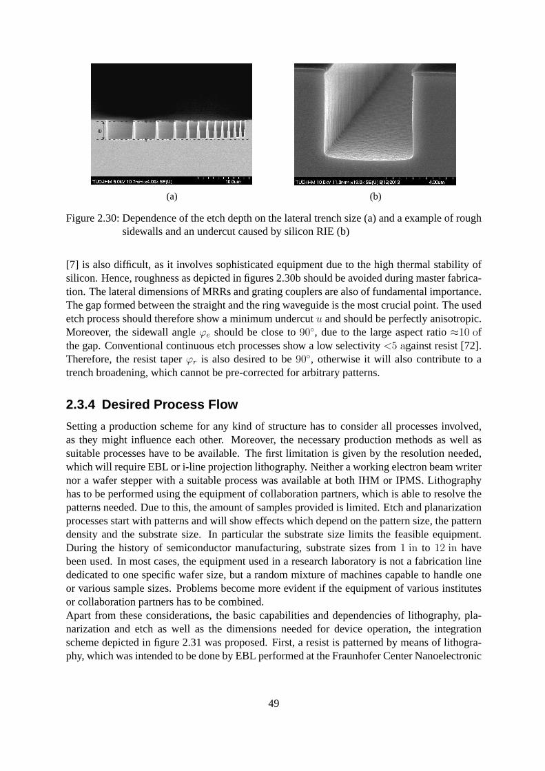
e
(a) (b)
Figure 2.30: Dependence of the etch depth on the lateral trench size(a)and a example of roughsidewalls and an undercut caused by siliconRIE (b)
[7] is also difficult, as it involves sophisticated equipment due to the high thermal stability ofsilicon. Hence, roughness as depicted in figures2.30bshould be avoided during master fabrica-tion. The lateral dimensions ofMRRsand grating couplers are also of fundamental importance.The gap formed between the straight and the ring waveguide isthe most crucial point. The usedetch process should therefore show a minimum undercutu and should be perfectly anisotropic.Moreover, the sidewall angleϕe should be close to90◦, due to the large aspect ratio≈10 ofthe gap. Conventional continuous etch processes show a low selectivity <5 against resist [72].Therefore, the resist taperϕr is also desired to be90◦, otherwise it will also contribute to atrench broadening, which cannot be pre-corrected for arbitrary patterns.
2.3.4 Desired Process Flow
Setting a production scheme for any kind of structure has to consider all processes involved,as they might influence each other. Moreover, the necessary production methods as well assuitable processes have to be available. The first limitation is given by the resolution needed,which will requireEBL or i-line projection lithography. Neither a working electron beam writernor a wafer stepper with a suitable process was available at both IHM or IPMS. Lithographyhas to be performed using the equipment of collaboration partners, which is able to resolve thepatterns needed. Due to this, the amount of samples providedis limited. Etch and planarizationprocesses start with patterns and will show effects which depend on the pattern size, the patterndensity and the substrate size. In particular the substratesize limits the feasible equipment.During the history of semiconductor manufacturing, substrate sizes from1 in to 12 in havebeen used. In most cases, the equipment used in a research laboratory is not a fabrication linededicated to one specific wafer size, but a random mixture of machines capable to handle oneor various sample sizes. Problems become more evident if theequipment of various institutesor collaboration partners has to be combined.Apart from these considerations, the basic capabilities and dependencies of lithography, pla-narization and etch as well as the dimensions needed for device operation, the integrationscheme depicted in figure2.31was proposed. First, a resist is patterned by means of lithogra-phy, which was intended to be done byEBL performed at theFraunhofer Center Nanoelectronic
49

II. Silicon Etch + Resist StrippI. Resist Patterning III. SiO Deposition2
IV. SiO Polishing2 V. Resist Patterning VI. Silicon Etch
MRR with Gap Reflector Coupler
Silicon Resist Silicon dioxide
AA
Figure 2.31: Desired process flow for the fabrication of a multilayer silicon imprint master ex-hibiting section through aMRR gap as well as a grating coupler with adjacentwaveguide reflector
Technologies (CNT)and, as a back-up solution, using i-line stepper lithography in collabora-tion with SAW components GmbH. The resulting soft-mask was subsequently transferred intosilicon byRIE with an etch depth of the desired single-mode waveguides. Inorder to performa second lithography step, the surface has to be planarized.A resist layer which is afterwardsspun-on this planarized surface will show less thickness disturbances and therefore allow fora better dose to size controllability as well as homogeneityduring exposure. In order to re-duce the substrate’s topography height, it is conformally first covered with silicon dioxide usingPECVD. Afterwards this is selectively removed from the protrusions usingCMP. The secondlithography step is again performed by the respective collaboration partners. The overlap accu-racy between the two lithography steps can be relatively low, as long as the absolute positionbetween structures in both height levels has no crucial importance as resist trenches can overlapinto the regions patterned in the first step. In the followingetch step, these regions will not betransferred, as they are filled with silicon dioxide which shows low removal rates during siliconetch (cf. detail A in figure2.31). After the second etch step, silicon dioxide can be selectivelyremoved from silicon using buffered wet etch. As result, thedesired master structure with twoindependent height levels can be obtained.
50

2.4 Nanoimprint Lithography
NIL is a patterning technology. In contrast to all optical lithography technologies,NIL isnot limited by diffraction and can reach sub-10 nm resolution. In contrast to many other ap-proaches,NIL will not be used in its common sense here, thus as a lithography technology, butas a direct patterning method (DP-NIL). For this variation, the patterns do not serve as masklayer for subsequent process steps, but are directly used asfunctional elements. In analogy toother lithography techniques there are many factors which change the patterning results. Thesewill influence the operation and efficiency of the produced elements, which are envisaged tomanipulate light in the present case. Table2.3 tried to give an overview of process tolerancesfor the desired design. In addition to the factors characterizing nearly every patterning process(resolution, line edge roughness, sidewall angle, registration and overlay, ...), the formation ofa residual layer and its thickness homogeneity are inherentto NIL. TheRLT optimization aswell as compliance with a certain defectivity and yield level are main factors of process devel-opment. The following section focuses on some of the factorswhich will influence the resultswith respect to the desired integrated optical elements. The aim of this work is to show a proofof principle. Therefore, neither the optimization of process times, nor the yield is discussed indetail, unless it has a significant influence on the obtained results.
As the first publications onNIL date back to the early 1990’s, a giant variety of processes,materials and machines were proposed, developed and tested. If a solution for a specific prob-lem has to be found, one does not only have to take into accountif a production technology iscapable to solve the problem, but also if it is available. Similar to the master fabrication, theproblems increase, if a complete process needs to be set up and a variety of compatibility issueshave to be taken into account as well.MRRs and grating couplers are fabricated using direct patterning UV-assisted nanoimprintlithography within this work. The use of UV-curable polymers was first proposed for the repli-cation of compact discs [111] and since then it has emerged either for direct patterning or forlithography.UV-NIL can be either done on a wafer-scale [112] or in a step-and-repeat manner[113]. Using waver-scale printing, a full wafer is patterned within one imprint step, mostlyreplicating several chips with the same layout at once. In contrast, a single chip can be re-peatedly imprinted in different positions of a wafer, each time performing a complete imprintstep. The latter is the one mainly followed here, for three main reasons: Firstly, as explainedin section2.3, the production of a suitable master is a sophisticated task. It involves severalprocess steps, where effort and cost scale with the patterned area. As step-and-repeat imprint-ing is capable to pattern a small chip several times on a wafer, this is a viable route. Secondly,the development of a step-and-repeat imprint process was the main focus of an accompanyingPhD work, which enables the extensive use of previously acquired knowledge. Thirdly, the onlycommercial imprint tool available atIHM andIPMS is a NPS 300 (SET / Süss Microtec).
2.4.1 Step-and-Repeat UV Nanoimprint
The repeated imprint of single chips on one substrate is possible for both,UV-NIL andT-NIL.TherebyT-NIL requires the stamp and the substrate to be heated separately. A rather largethermal load, resulting in temperatures above or close to the resist’s glass transition temperature,
51

may lead to pattern deterioration of adjacent imprint sites. UV-NIL is therefore preferable unlessit implicates other restrictions which will be partly reviewed below.
Resist ApplicationTo perform an imprint on a substrate, first of all a resist has to be applied. Generally, twomethods are commonly in use: spin-coating as well as drop-on-demand dispensing. The mostsuccessful version of the latter in commercial terms is alsoknown as step-and-flash (SFIL),mainly used by Molecular Imprints [113]. Therewith the local resist volume can be adjusted toa given layout. The exposure of adjacent sites is not of interest, as the material can be appliedprecisely in the chip site currently interesting for patterning. The defined application of resistby drop-on-demand dispensing is a comparatively difficult task, which involves the use of aspecial dispenser unit. The operation conditions have to beadjusted to the specific imprintresist. Alternatively, spin-coating can be used. This doesnot involve sophisticated equipmentand is a matureIC manufacturing step. Providing that the substrate is flat andshows the samesurface chemistry, the resulting resist amount will be equal all over, apart from the inherentformation of an edge-bead.
Cavity Filling and Residual Layer ThicknessImprint cavity filling can be considered on two levels. Firstly, the resist interaction with a singlepattern can be considered. Hereby, the interactions of the resist with the cavity geometry haveto be taken into account. Additionally, a respective pressure originating from the compressionof the trapped air may be considered. Most of the considerations shown in literature are barephenomenological descriptions or are done by numerical simulations e.g. [114, 115]. The latterusually largely vary in terms of approach and scalability.For cavity sizes much larger than the involved resist molecules, two basic mechanics are rele-vant: capillary filling and squeezed flow. Both mechanism varyin the origin of the forces whichdrive the polymer to fill a cavity. If the contact angle of the resist and the mold surface is smallerthan90◦, capillary forces will try to minimize the unwetted mold area once the resist has enteredthe cavity. Hence, the tendency of the system to form an energetically favorable state fills thecavities. The necessary material has to be acquired from theresidual resist layer underneath themold protrusions. The flow within these gaps is limited by viscosity, residual cavity height andlength. Thereby, the filling might be hindered and an external pressure has to be applied to forcethe polymer to enter the cavities. In this case, the viscous nature of the resin will dominate thefilling process and a squeezed flow has to be present. The pointat which one or the other effectdominates depends on the specific system, which is, among others, influenced by contact anglebetween resist and mold.The viscosities of thermoforming resins above their glass-transition temperature are signifi-cantly higher (> 10 kPas) than those of thermosetting resists forUV-NIL (< 100 mPas) [116,117]. Moreover,UV-NIL resists usually show a contact angle of< 90◦ even on molds withappliedASL [117]. They therefore pronounce capillary induced filling.
Another goal of an imprint process is to yield a certain residual layer thickness and homo-geneity. This is of tremendous importance to the patterns considered here, as the device per-formance will be strongly influenced by the exactRLT (cf. section2.2.2.2). As the focus is onstep-and-repeat imprint in spin-coated films, the pattern density will have a significant influence
52

upon the residual layer. The understanding of the underlying effects is therefore of importance.The application of the aforementioned algorithms for the simulation of cavity filling is usuallyimpossible for the large areas of interest, e.g. an entire chip to be imprinted. The considerationsin the following show more or less generalized trends. A detailed analysis, e.g. of a spatiallyadjusted resist amount, the use of dummy fill patterns as wellas the mold stack architecture,is essential for imprint optimization, however it was not performed during this work due to thelack of time.
The basic fluid mechanical equations to handle theRLT are similar to the ones used forcavity filling. Based on the general Navier-Stokes equation,abstracted models, e.g. coarsegrain, are usually applied in order to consider theRLT within large areas [118–120]. In contrastto the cavity simulations, the limited mechanical strengthof the mold and substrate, i.e. theirdeformation during imprint, has to be taken into account. Based on the adapted Navier-Stokesequation given in [119] one can give the polymer flowq within a slab of heighthrlt by
q ∝ h3rlt∆p
µlc, (2.27)
whereµ is the resist viscosity andlc is the channel length. This is similar to the well-knownHagen-Poiseuille law describing the fluid flow within a tube.Note that this is a rough approx-imation, as the resist viscosity is not a constant parameter(e.g. shear thinning [121]) or thematerial is able to slip along the mold-resist interface [122].However, equation (2.27) allows some general conclusions. The polymer flow within the resid-ual layer is needed to fill the cavities but also to reduces itsdeviation. The smaller the respectiveflow, the longer are the imprint cycles to achieve a certain constraint. The slab thicknesshrlt
has a major influence. It should therefore be as large as allowed for any given application. Irre-spective of this, a resist flow within a slab will only start when a pressure difference is present.Note that this pressure is not equivalent to the applied imprint pressure, as a homogeneouspressure distribution along the entire imprint area will not cause any pressure difference whenthe cavities are already filled. A pressure difference will usually arise if either the mold or thesubstrate are deformed. The resulting∆p is thereby related to the deformation, thus theRLTinhomogeneity, and the mechanical strength of the system, mainly given by Young’s moduli ofthe stacks materials. To be able to achieve a minimal inhomogeneity, Young’s moduli shouldbe as high as possible. This is contrary to the intrinsicallylow elastic modulus of polymer moldmaterials. Note that a pressure difference may also arise from flatness deviations of mold andsubstrate.Equation (2.27) further implies that it is generally desirable to reduce the area between trencheswhich have to be filled in the master, as this will reducelc. This is of crucial importance for theDP-NIL of optical chips. These will usually show sparsely placed trenches and a rather smallpattern density of below5 % [59]. Adjusting the pattern density may be a viable route to reduceimprint times and residual layer thickness imhomogeneities.A specific problem of step-and-repeat patterning is the presence of a confined imprint area.Inherent to this is a pressure drop at the chip edge. This willlead to a resist flow from theresidual layer into the unrestricted outer region. Hence, the RLT will be non-uniform in thechips outer area with a reduced resist thickness at the edges. Note that the pressure difference in
53

this case correlates with the applied imprint pressure instead of the mold/substrate deformationmentioned before.
RLT optimization during imprint is only possible if theRLT can be measured. Numerousmethods have been proposed to asses theRLT of a patterned surface. An easy way is to cleavethe sample and observe the cross-section. However, this includes sample destruction and doesnot allow in-line quality control. Further it requires a rather high preparation effort, as theobservation of dimensions< 100 nm requires aSEM. Stylus profilometry can be used but alsoincludes pattern demolition. Alternatively, optical methods are capable to monitor small filmthicknesses. In-situ and real-time measurements are possible if a suitable setup is present.Possible methods range from white light reflectometry over scatterometry to x-ray diffraction[116]. Most of the methods aim to measure theRLT in an area with patterns in or close tothe sub-wavelength region. For the structures considered here, a white light reflectometer, asconventionally used to determine slab thicknesses in semiconductor manufacturing, is sufficient.
Imprint PolymersMost of the resins used forUV-NIL are radically curing. Molecular oxygen is well knownto inhibit the polymerization or cross-linking especiallyof acrylate-based mono- or oligomers[123]. Depending on the conditions, present oxygen will partly or fully scavenge the generatedradicals. Thereby a resist film will not or not completely be solidified. As the absence of oxygenwill eliminate the issue, either the operation of the imprint within vacuum, or the purge of anactive imprint site with inert gases might be used. For the latter carbon dioxide seems to bemost effective [124].However, for step-and-repeat imprinting in spin-coated films, oxygen inhibition might be usedto avoid the undesired curing of adjacent imprint sites during exposure [58]. In any case, theexposure of adjacent imprint sites has to be minimized. Special measures have to be taken toaccount for this. As the illumination within most UV-imprint systems diverges, apertures asclose to the resist as possible have to be used.
Another common feature of radically curing resins is the inherent shrinkage. Many publica-tions mention this to facilitate the demolding, as the patterns within the cavities do not showdirect contact with the mold after curing, e.g. similar to the results depicted in figure4.2.However, shrinkage will change the features’ dimensions (e.g. [59, 75]). This is especiallyimportant forDP-NIL. A pre-compensation requires precise knowledge of the shrinkage and isfurthermore not possible for arbitrary pattern layouts.
2.4.2 Anti-Sticking Layers and Adhesion Promoters
NIL includes a mechanical contact of the mold and the resist. This is a critical issue if the resistpatterns should be detached from the mold. During the demolding of a pattern, forces will tryto keep it in its original position. In principle, two failure mechanisms can occur. Firstly, theinterface of the resist to the substrate can break, thus an adhesive break happens. Secondly, theresist can break internally, leaving a residual resist layer or a part of the pattern on the substrate.The resolution of adhesion and cohesion issues is one of the main challenges ofNIL, which is amajor topic in many publications and is still under discussion. Generally, one has to distinguishbetween defects caused by microscopic interactions of substrate, resist and mold pattern, or the
54

defects originating from the rather macroscopic demoldingstrategy. The latter can e.g. induceadditional shear forces deteriorating the imprint results. Often they can be avoided by a dedi-cated demolding process, which may include additional tooling.If the focus is on the microscopic interactions, there are different ways to tackle defects, de-pending on their nature. If a cohesion break occurs, it is possible to either change the resist, orto reduce the interaction forces at the mold-resist interface. The latter applies if resist-substrateadhesion fails. The use of Ormocore as resin is indisputable. Fortunately, the adhesion of thisresist to a silica surface seemed to be sufficient in all previous works atIHM. Moreover, addi-tional adhesion promoters are commercially available.On the contrary, the interaction between the resist and the mold should be as small as possible.A broad variety of effects may be responsible for forces thathinder a pattern from mold release.They range from a purely mechanical nature, e.g. interlocking or friction, physisorption, rep-resented by interphase diffusion and adhesion, to chemisorption, thus a covalent bond betweenresist and mold [9]. Determination of the individual effects is a difficult task. A common mea-sure to assess the surface properties of a material is itssurface free energy (SFE).Different measures have been proposed to reduce theSFE. Most prominent are functionalsilanes. These are able to covalently bond to a hydroxyl group on the surface. As a self-limitingprocess, it is able to form conformal monolayers [125]. Functional groups can be connected tothe silanes to modify surface properties. Perfluorated silanes like1H,1H,2H,2H-perfluorodecyl-trichlorosilane (F13-TCS)have proven to be best suited due to their low resultingSFE.Most of the forces acting on a pattern during demolding will scale with the surface area. Hence,as the mechanical strength depends on the lateral cross-section, the stability is connected withthe patterns’aspect ratio (AR). Generally, patterns with higherAR will be more prone to de-molding defects.
2.4.3 Polymer Molds
The use of polymer molds, cast from a master, offers some advantages compared to the use offused silica molds conventionally used inUV-NIL . As already mentioned, polymer molds canbe cast from many different master materials.UV-NIL requires either the substrate or the moldto be UV-transparent. As the transparency of the substrate is mostly driven by the application,UV-transparent molds are preferable. If UV-transparent molds are used, the master materialdoes no longer have to be fused silica, but can, amongst others, be silicon. This enables eas-ier processing, higher lateral resolution and larger aspect ratios. Additionally, a polymer moldcast involves lower pressures than the ones needed to perform an imprint, because theRLT canbe large compared to the protrusion height. Therewith, the possibility to damage a valuablemaster pattern is reduced. In addition, polymers usually show a lower Young’s modulus thanfused silica and are flexible to some degree. Therewith, e.g., printing over particles [126] andthe replication of features with undercuts [127] become possible. Furthermore, some polymermold materials show an intrinsically lowSFE. The application of an additionalASL might notbe necessary. This simplifies the process flow and may also avoid ASL degradation during im-print, as the lowSFEis an intrinsic material property.The usage of polymer molds also degrades some imprint parameters and causes additional prob-lems. The comparably low Young’s modulus of a polymer mold yields unwanted feature defor-
55

mation. This may influence the patterns and theRLT during imprint as well as mold cleaning.Especially high aspect ratio mold patterns are prone to feature collapse. Moreover, mold poly-mers chemically differ from fused silica, which may induce additional effects.The following will summarize potential problems induced bypolymer molds during an imprintas well as a cleaning process.
2.4.3.1 Imprint
To push liquid resist through a cavity, a pressure difference has to be present (cf. eq. (2.27)).The pressure difference within a mold is generated by a mechanical deformation of the molditself. If a bulk polymer mold mounted on a rigid support is considered, the deformation islimited to the polymer. In any case, the pressure caused by a deformation will by related to theYoung’s modulus of the mold material. As consequence, a higher Young’s modulus will helpto reduce theRLT inhomogeneity, which is highly desirable for mostDP-NIL applications.Unfortunately, polymer mold materials with arbitrary mechanical properties are not available.In principle, the imprint mold, including its complete stack, should be as stiff as possible. Thisincludes mold polymers with high Young’s modulus.
Mechanical DeformationsMechanical deformations are widely observed in contact printing [45, 128, 129]. Figure2.32depicts two extreme examples of sagging or roof collapse andbuckling. The description of
p
(a)
p
(b)
Figure 2.32: Mold deformation caused by an external imprintpressurep: roof collapse or sag-ging (a)as well as buckling(b)
feature collapse duringNIL is more complicated, as the resist-mold interaction as wellas theresist flow and pressure distribution have to be taken into account. In general, the same defectsoccur, but the specific conditions differ. Deliberate feature collapse can also be used to fabricatecomplex structures like blazed gratings [130]. Even if the involved forces are not large enoughto cause defects like depicted in figure2.32, a mechanical deformation in polymers is morelikely than in fused silica due to the lower Young’s modulus.High aspect ratio patterns withinthe mold are more prone to a possible deformation. For the desired MRR structure this is ofcrucial importance, as the gap region will showARs of up to10 as already mentioned. Figure2.33ashows the gap of aMRR in a top-down view. A polymer mold with a Young’s modulusof ≈ 120 MPa was used. Unfortunately, the applied pressurep used for imprinting, cannotbe reduced to allow for defect-free imprinting. Similar to the results which will be shown insection3.4.2, the resist can be pinned at any edge of a trench in the mold. Toovercome thispinning barrier, an external pressure needs to be applied. The necessary pressure depends on the
56

(a) (b)
Figure 2.33: Defects due to the mechanical deformation of a non-rigid mold material: gap de-formation of aMRR (a) and the same in combination with incomplete structurefilling (b) (parameters: MD 700, Ormocore(a), MD 700, mr-UVcur06 (MRT) (b))
trench geometry and dimensions as well as the contact angle of the resist to the mold material[131]. Figure2.33bshows the deformation of aMRR gap in conjunction with a filled ring andan unfilled waveguide. For the unfilled waveguide, the resistshows resist pinning at the patternentry edges.
Anti-Sticking LayersOne major topic considered within this thesis is the transition from fused silica to polymermolds. Previous works usedF13-TCS ASLson top of silicon or silica molds. The forces origi-nating from the resist and polymer mold interface have to be determined. If theSFEof the usedmold material is too large, it may be reduced by the application of additional coatings. Silane-basedASLs will be applicable if hydroxyl groups are present on the polymer mold surface.This is possible for some commercially available materials[132]. Special attention has to begiven to the hydroxylation of a mold surface. For silicon or silica stamps, this can be performedusing sulfuric acid. This is not possible with polymers, as they will be partly or completelydegraded. Alternatively, hydroxylation using an oxygen plasma treatment can be performed.The O2-plasma may also attack the polymer mold, hence change the pattern shapes or at leastincrease the roughness [9].An elegant way to avoid any kind ofASL are mold materials which show intrinsically lowSFEvalues. As mentioned above, theSFEis not able to account for the complete resist mold interac-tion, e.g. the formation of covalent bonds. Additionally, the diffusion of solvents into polymersand their swelling is a well-known problem with mold polymers like PDMS. Nevertheless, re-sist components may also be able to access the mold’s polymernetwork. Forming this kind ofinterphase instead on an interface probably also accounts for a mold degradation [9, 133].
ShrinkageThe polymers used as molds show shrinkage similar to the one observed within thermoset-ting resists. It is difficult to determine the shrinkage of a specific polymer. Different methodsare proposed in literature, mostly to give a lateral shrinkage value under different constraints
57

which are specific for the used process. Commercially available mold polymers can show abulk volume shrinkage of3 to 10 % [134].The shrinkage observed in a bulk polymer does notnecessarily have to be the same as in patterns. Commonly, the largest amount of shrinkage isassumed to occur in the out-of-plane direction [75]. However, lateral shrinkage is not negligi-ble. When a soft mold is used for imprinting, the out-of-planeshrinkage values of both, moldpolymer and resist, do accumulate. If a precise structure height has to be achieved, as requiredfor the grating couplers (cf. eq. (2.20)), the master pattern must be pre-corrected dependingon the shrinkage. Lateral shrinkage occurring during mold cast will compensate the one of theresist to some extent. Nonetheless, two issues remain: first, due to the restricted movement,the lateral size change at the bottom and the top of a pattern differ [59]. This leads to taperedsidewalls even if the ones of the master are perfectly vertical. Compensation for this duringmaster fabrication would involve a precise sidewall angle tuning also in the range larger than90◦. Moreover, the absolute lateral shrinkage not only dependson the relative one, but alsoon the lateral pattern dimensions. It is impossible to fullypre-compensate for this in arbitrarylayouts, as for example in theMRRs’ gap regions.
Gas and Material DiffusionIn contrast to silicon or silica, polymers show an increasedpermeability for gases and solvents.This property can have numerous different implications. One is the already mentioned diffusionof resist materials or their components into the mold. When molds are stored and processed un-der ambient air conditions, i.e. oxygen is able to diffuse into the mold. If an imprint is conductedwith such a mold, the oxygen can again diffuse out of the mold into the resist. If a radicallycuring resist is used, oxygen scavenging may be observed. Depending on the sensitivity of theresist and the oxygen molecules’ mobility, completely or partly uncured resist patterns are theconsequence. An example of such an effect is depicted in figure 2.34. To overcome this issue,resist and mold may be adjusted or, alternatively, the entire imprint setup is operated under theabsence of oxygen, hence, under vacuum or inert gas purge.On the other hand, an enhanced gas diffusion into the mold is highly appreciated during the
(a) (b)
Figure 2.34: Uncured resist residues originating from oxygen inhibition caused by oxygen dif-fusion from a polymer mold(a) and the same structures replicated from the moldafter it was purged with nitrogen for10 min (b); note the sharp edges in(b) incontrast to(a) (MD 700 mold, MINS 311 RM resist)(b)
58

imprint process. It helps to avoid filling defects, as the gasremaining within cavities can diffuseinto the surrounding mold. If silicon or silica is used as a mold material, special measures like ahelium purge [58], which is able to also diffuse into the fused silica, or gases condensing duringimprint [135] may be necessary.
2.4.3.2 Cleaning
Mechanical defects on polymer molds do not exclusively occur during imprint as discussedabove. In some cases, the replication of master patterns into a mold and the subsequent sec-ond replication into a resist are possible without defects,but after mold or resist cleaning, thepatterns are collapsed as sketched in figure2.35a. Here, conditions comparable with the onesleading to pattern collapse during resist development [136, 137] can evoke persistent featuredeformation. Unless this effect is used for the generation of special patterns [138], it has to beavoided. The following considerations are also part of a master’s thesis [139] and are furtherpublished as a paper [140].A cleaning step is used to remove particles or uncured resistresidues from the mold or the re-sist patterns. Uncured resist is a common problem inUV-NIL due to oxygen scavenging and inparticular during step-and-repeat imprint in spin-coatedfilms, as not the entire resist is exposed.Mold cleaning is also required if polymers molds are used. Mold casting is an elaborate andcostly process. Usually special templates and processes are required for polymeric molds to becompetitive with rigid stamps in terms of resolution, flatness, residual layer thickness, etc. (cf.section3.3). Simple replication of master structures in a polymer is not sufficient to gain high-quality imprints. Therefore, the lifetime of a mold should be as long as possible. Cleaning isan easy way to remove uncured resist residuals or particles which may damage the mold duringimprint.
A stability prediction of mold or resist patterns is highly desirable and will be presented inthe following. The modeling of the structures has been done using two different approaches.Energy-based calculations are performed on pillar structures. Furthermore, deformation analy-sis using the forces generated by the meniscus between structures at a liquid-air interface andthe restoring force given by the deformation of elastic gratings were performed.In general, two different failure mechanisms can occur. If the spacing between structures islarger than their height, they can stick to the ground after cleaning. This is called ground col-lapse [141]. If the features are dense enough, i.e. the spacing betweenthe features is smallerthan twice their height, a lateral collapse [142] may occur. Thereby, the structures stick to eachother rather than to the ground. Cylindrical patterns as depicted in figure2.35b, showing aspacing between the pillars that is larger than twice their height, are considered. Therefore,only a ground collapse can occur. The critical aspect ratio of the pillars, given by the ratio ofthe structure heighth to the lateral dimensiond, can be expressed by [141]:
h
d=
π5
3
211
3 31
2
(
1− ν2)− 1
6
(
Ed
2γs
)2
3
(2.28)
whereE is the Young’s modulus,ν the Poisson’s ratio andγs the SFEof the mold material.A similar analysis can be performed to describe the lateral collapse due to adhesion of dense
59

I. ontaminated oldC M II. leaningC III. attern ollapseP C
Polymer C Aleaning gentParticle U Rncured esist
(a)Pillar - Dense Grating
d
Pillar - Sparse
h
d
h
Λ glgs
(b)
Figure 2.35: Cleaning of a polymeric mold containing particles and uncured resist residues us-ing a cleaning agent and a potential feature collapse(a) as well as a sketch of theconsidered structures: sparse and dense pillars as well as dense gratings with theirrespective dimensions used for simulation(b)
pillars to each other. This leads to a critical aspect ratio of [142]:
h
d=
(
33
4πE(Λ− d)3
2
21
432γs (1− ν2)1
4 d1
2
)1
3
(2.29)
whereΛ denotes the pitch of the structures as depicted in figure2.35b.For the forecast of the stability of grating-like patterns,a simulation of the capillary force and
the resulting deformation of the structures can be performed. After mold cleaning, the cleaningagent has to be removed from the mold surface. If no additional effort, e.g., supercritical drying[143] is taken, the liquid will evaporate. During evaporation, at some point, the close liquid filmdisrupts atop the features and only the cavities stay filled.If the liquid evaporates further, it ispossible that one cavity is still wet while the adjacent cavities are empty. In this case, strongLaplace pressure forces would cause a pattern collapse. In contrast, also weak capillary menis-cus forces of adjacent filled grating cavities evoke patterncollapse [142, 144]. Meniscus forcesarise in the cavities where capillary bridges are formed. The meniscus curvature is specific forthe combination of liquid and cavity material. The pressuredifference∆p acting on a structureis given by [145]
∆p = 2γl cos θ
(
1
gs− 1
gl
)
, (2.30)
wheregs denotes the lateral dimension of a small cavity surrounded by two larger cavities ofthe widthgl as depicted in figure2.35b. θ is the contact angle between the cleaning agent andthe mold material andγl represents the surface tension of the rinse liquid. If all structures ina grating and the formed capillary menisci and hencegs andgl are equal, the pressure differ-
60

ence vanishes and the grating is in an equilibrium state. Thedifferences in capillary bridges ofadjacent cavities in a grating, caused by fabrication or handling differences, lead to an initial de-flection and, therefore, to a pressure difference∆p acting on the structures. An equilibrium hasto be found between these and the restoring forces generatedby the deformed feature. Previousworks mainly focused on the description of resist features on a substrate [136, 142, 145, 146].Usually, the used resist materials exhibit Young’s moduli that are by orders of magnitude smallerthan the ones of substrates like silicon (≈ 150 GPa) or fused silica (≈ 70 GPa). In this case,the deformation of the substrate can be neglected and only the deformation of the patternedresist structures will contribute to a displacement. For polymer molds, the substrate as well asthe structures are made of the same material. During deflection of a structure due to meniscusforces, the pattern itself as well as the substrate is deformed. Finite element method simula-tions using the ANSYS Workbench were utilized to determine the deflection of an all-polymerstructure with respect to a meniscus pressure difference (cf. eq. (2.30)) applied on its surface.The restoring forces of a given geometry have to form an equilibrium with those originatingfrom the different menisci of adjacent trenches (cf eq.2.30) as described in [136]. In this case,the structures reach a stable position before collapse. If the restoring forces are too weak, thestructures will approach until they touch each other, i.e.,collapse.The application and verification of the aforementioned equations is specific to the mold poly-mers used. As this involves a non-negligible amount of experimental data, all results are shownin conjunction in section3.3.
61

2.4.4 Desired Process Flow
Figure2.36 shows the general process flow as desired for imprinting.2.36 Here, the silicon
II. Mold SeparationI. Mold Casting
III. Resist Application IV. Imprint V. Demolding
Silicon Master
Polymer Mold
Imprint Resist
Substrate
Figure 2.36: Process flow for the replication of a silicon master structure in a polymer mold andthe subsequent imprint into a polymer
master which was fabricated using the process scheme as explained in section2.3.4, is castinto a working mold. Depending on the considerations explained above, the polymer’s Young’smodulus should be as high as possible. Moreover, it has to be compatible with the used resist,namely Ormocore. This includes the resistance of possibleASLs as well as UV transparency.Subsequently, the polymer mold can be used to perform an imprint in a spin-coated resist layer.The mold fabrication process may also allow to include additional apertures as close to themold surface as possible. Thereby, pre-exposure effects ofadjacent imprint sites induced bystray light can be effectively reduced [58]. After UV-curing the resist, demolding is performedwith a vertical force between substrate and mold to avoid defects. In a result, a resist layerpatterned within two height levels can be obtained which shows grating couplers andMRRswith the desired layout.
62
3 Experimental Results
The aim of the present work was not only the generation of design data for grating couplers.Moreover, the generated design should be turned into reality, hence a demonstrator should beproduced and, of course, characterized. The following chapter will show the transition fromdesign data to a real pattern. The considerations and process steps as depicted in sections2.3and2.4 are the basis. The straight order shown in the following sections suggests a sequentialprocessing of the individual tasks. This was not the case in reality. The presented results arethe outcome of multiple optimization processes. The chosenpresentation is thought to allow acomprehensive understanding of the process.
The master fabrication starts with a layout representation. Its generation will be shown insection3.1. This layout has to be transferred into a physical master structure which was cho-sen to be silicon. Lithography, planarization and etch are the three major steps which wereused. The desired patterns are rather complex and can becomecost-intensive. Most of the ex-perimental part was conducted with the equipment availableat IHM andIPMS. Lithographywas the only exception, as none of the partners has operational machines and processes able toresolve the required dimensions. The lithography part splits up into optical projection lithogra-phy andEBL. Stepper exposures in collaboration with SAW components GmbH were alreadyperformed in previous projects ofIHM and showed promising results. However, gratings withpitch of600 nm and, more importantly, isolated trenches with a size of200 nm are close to theresolution limit of the used i-line stepper and the available resist processes. Therefore,EBL wasused in parallel.After successful master fabrication, as described in section 3.2, a polymer mold has to be cast.Section3.3 gives an overview of the possible mold materials and template architectures thatcan be used. The fabrication processes are explained in detail and the obtained results are dis-cussed.After all these steps, the core part ofNIL, the imprint itself, can be performed. Section3.4describes the used imprint setups, which were partly utilized for mold production already. Dif-ferent schemes are discussed regarding their ability to reproduce the optical components withinthe given specifications.RLT optimization is one main issue discussed.Finally, the fabricated patterns were also characterized optically, which is described in section3.5. Therefore, the already existing measurement setup had to be extended to address the specialneeds of vertical coupling with gratings. The fabricated waveguides are briefly discussed beforegrating couplers are characterized regarding their positioning tolerance, transmission spectrumand, of course, efficiency. An analysis of critical points isperformed and can be exploitedregarding possible improvements of the design, layout and process later on.
Some processes were used throughout many parts of the experimental work and can thereforenot be attributed to a specific section. Most of them have neither been investigated nor optimizedregarding their use, but have been established previously.Nonetheless, it is worth giving details
63

for the sake of completeness.A scanning electron microscope S4700 (Hitachi) was used to take micrographs. It is difficult
to observe polymer patterns using aSEM. The polymers that were used are electrically non-conductive. Hence, electrons impinging on the surface are not distributed along the sample andsubsequently guided to the chuck. Instead, they accumulateand disturb the incident electronbeam. To avoid charging, less than5 nm of gold was applied on almost every sample shown inthe following with a S150B sputter coater (Edwards). If the observed patterns were used lateron, 1 g Gold Stripper 645 (Degussa) dissolved in40 mL deionized water was used to removethe gold. During this process, no measurable change in dimensions could be observed forOrmocore. A dedicatedSEM may be able to observe the polymer patterns without additionalconductive layers.Size data obtained fromSEM images has to be dealt with care. The magnification error ofthe SEM strongly depends on the used working conditions (magnification, working distance,grid orientation, ...) and can end up to variations of5 %. This is crucial if small changes in thedimensions, e.g. during shrinkage, are to be determined. A calibration for the specific operationconditions used for the measurements is inevitable if one isinterested in exact values.
The importance of a precise control of theRLT was already outlined in sections2.1 and2.2. RLT measurements were performed using a customized spectral reflectometer atIHM.This is able to carry out automated measurements on samples and wafers of up to200 mm.In addition, a NanoSpec 8000 (NanoMetrics) was used atIPMS. Necessary data to build aresist material model was acquired with ellipsometry usinga Rotating Analyzer VASE (J. A.Woollam Co. Inc.). A Cauchy fit was used for dispersion approximation. The reflectometerallows measurements with a spot-size smaller than5 µm depending on the used objective. Dataacquisition within the patterned area is possible for the layout which will be shown in figure3.2. Unfortunately, the stage has a very limited positioning accuracy of more than20 µm. Ifthe measurement spot fully or partly intersects with a pattern, the spectral response and thus thecalculated thickness is distorted. Post-measurement datafiltering was applied to delete thesedata points. The reflectometer can further be utilized to measure the silicon dioxide thicknessafter PECVD andCMP (cf. section3.2.3). Furthermore, it allows to approximate the opticalpath within the bottom reflector of the final chip (cf. section3.5.3.2).
Section2.4.2 has already outlined the importance of surface modifications to NIL, eitherto enhance or reduce the surface interactions. The processes used here are based on elabo-rate work on the evaluation and qualification of different anti-adhesion measures and adhe-sion promoters [147, 148]. As a result, silane-based surface modifications were performed.1H,1H,2H,2H-perfluorodecyltrichlorosilane (F13-TCS) was used to reduce theSFE of a sur-face, hence, to form anASL on the surface. BeforeF13-TCS can be applied to the surface,hydroxyl groups have to be generated. This surface hydroxylation was performed either byoxygen plasma treatment within a Plasmalab 80 PLUS (Oxford)or a C012 (Surface Technol-ogy Systems). Alternatively, in case of inorganic substrates, H2SO4/H2O2 cleaning was used.Afterwards,F13-TCSwas applied in a customizedmolecular vapor deposition (MVD)chamberunder vacuum (≈ 10 mbar) and elevated temperature (≈ 90 ◦C). The full process details aredescribed in [9]. The samples could be used without any further cleaning steps after deposition.
Throughout the entire work, cleaning processes had to be performed many times. Variouswet cleaning methods like a simple solvent flush, the removalof organic contaminations using
64

H2SO4/H2O2, automated cleaning using several spin-rinse-dryers (depending on the wafer size)and mechanical cleaning using a Cleaner 812 brush-cleaning station (G&P Technology) wereperformed. Throughout all these processes, the use of ultra- or megasonic cleaning was avoidedto suppress pattern deterioration like depicted in figure3.1. Alternatively, the aforementioned
Figure 3.1: Bare silicon master showing a waveguide reflector(pitch600 nm, height≈ 2.8 µm)which was damaged due to ultrasonic cleaning
Plasmalab 80 PLUS or a C012 could also be utilized to strip polymer residues using an oxygenplasma. This was particularly useful to remove residues of fluorinated polymers.
65

3.1 Layout Generation
In order to be able fabricate a structure by the already presented lithography techniques insection2.3.1, the patterns must be available in a layout representation.This is mostly a vector-based file format (gds, cif, ...). For the generation of the layout a free software tool namedKlayout was used [149]. The chip size was set to10× 10 mm2 given by the supported stampsize and the production effort. 16 sub-chips with a size of2.5× 2.5 mm2 were defined. Eachchip shows individual transmission lines either with simple waveguides orMRRsin an add-dropconfiguration as well as grating couplers. Parameters of thegratings were varied accordingto the 3 dB values given in table2.3. Moreover, the lateral dimension of the ring gap, thewaveguide width as well as the taper geometry were subjectedto a parameter sweep to be ableto extract as much data as possible by the fabrication of onlyone valuable master. The principlelayout is shown in figure3.2a. Note that there are two general types of sub-chips: the firstthree
5 mm
(a)
100 µm
Reflector Coupler Taper
(b)
Figure 3.2: Layout representation of the silicon master with 4× 4 sub-chips, where the rightcolumn showsMRRs, (a)and a close-up of a representative coupling section with awaveguide, taper and caption (red), the grating coupler andreflector (magenta) anddummy patterns (blue)(b)
columns from the left contain straight waveguides with grating couplers only, whereas the rightcolumn also contains ring resonators.Dummy patterns, as depicted in blue in figure3.2b, were added to the layout to account for twomajor problems. Firstly, the pattern density was increasedto prevent dishing of isolated linesduring theCMP process. Secondly, the dummy patterns were inserted to fill sparse parts of thelayout. This was intended to reduce the distances along which material has to be transportedduring imprint. Minimum distances between a waveguide and any kind of adjacent patterns arelimited by evanescent field coupling losses. These are comparable to substrate losses as givenin figure2.20. A minimum unpatterned safety margin of10 µm was present around any opticalelement.
66

3.2 Silicon Master Fabrication
For the silicon master fabrication process as proposed in figure2.31, most parameters influencethe overall result and even the subsequent steps interdependently. Sometimes several processesinfluence one parameter of the silicon master. E.g., the resist sidewall angle obtained fromlithography influences the sidewall angle within the masterin conjunction with the selectivityand the sidewall inclination resulting from the etch process. In some cases, effects originatingfrom one process step can be pre-compensated within a previous one. For the mentioned exam-ple, the layout patterns can be adjusted to yield patterns which are on their target value.Throughout silicon master fabrication, some pre-compensations were made and are mentionedin the text. The necessary data for the applied corrections was mostly acquired through testruns with a similar setup as targeted. Most of the results arenot given here in detail. Someof the results shown in the following are partly published within a paper [150]. Moreover, theconsidered processes were also used to fabricate master patterns used elsewhere [151, 152].
3.2.1 Electron Beam Lithography
The electron beam exposures described in the following wereperformed in collaboration withtheCNT. A SB3050DW (Vistec) variable shaped beam writer was utilized. The ability of thewriter to handle wafers of different sizes is limited.300 mm wafers are the standard substratesize, but200 mm wafers can also be handled, which was done to ensure a certaincompatibilitywith the equipment atIHM.The selectivity of the previously usedRIE process (cf. section3.2.4) to known resist materialsis comparably low (< 5 ). This made the use of thick resist layers necessary. Due to the patterndensity on the master, a chemically amplified negative tone resist with a thickness of> 850 nmwas used in the first patterning step, i.e. to build the waveguides. For the grating couplerspatterned in the second step, a positive tone chemically amplified resist with a thickness of450 nm was used. A primer layer underneath the positive tone resistensured good substrateadhesion.
Resist SidewallsThe resist used for the first exposure showed significantly tapered sidewalls like depicted infigure3.3a. For the relevant values of the most critical point in the first layer, theMRR gap, thistaper is nearly independent of pattern size, as can be obtained from figure3.3b. For trencheslarger than200 nm the sidewall angle is approx.80◦. The etch process only shows a finiteselectivity between resist and silicon removal, which was in this case approx.5.2 for an etchprocess similar to the one shown in [72]. So additionally to the taper, which is generated by theetch process itself, the resist mask degradation leads to a further sidewall inclination. However,the taper resulting from the available etch process was already around85◦. Based on the influ-ence of a tapered sidewall on the waveguide operation (cf. figure2.5b) and on the gap of theMRR, it was decided to set the target waveguide widthwwg at the half of the waveguide depthhwg. This led to an etch bias of−69 nm per edge, i.e. smaller resist lines. In addition, the dosewas adjusted to yield the dimensions given in the layout.A similar analysis, including resist characterization, was performed for the second resist layer,
67

(a)
0 100 200 300 400 500 6000
200
400
600
800
1000
Design CD (nm)
Measure
d C
D (
nm
)
wt
wb
wt dense
wt iso
wb dense
wb iso
(b)
Figure 3.3: Dense features in an850 nm thick negative tone chemically amplified electron beamresist showing tapered sidewalls(a)and a dependence of the top and bottom widthsof trenches using this resist(b)
which is used to pattern the grating couplers. It is a positive tone resist and hence, the ex-posed features will translate into trenches, rather than protrusions as for the first step. A biasof 18 nm was added resulting in wider resist openings. Again, the dose was adjusted to yieldtarget matching with the layout. The measurements were performed using a Verity 4i CD-SEM(Applied Materials) for resist top-down imaging and an S4700 (Hitachi) for cross-sections.In addition, the exposure strategy had to be optimized. First results showed significant shotboundaries. These occur when a layout pattern is stitched together from two or more projectionprimitives. Examples are barely visible as disturbances occurring at two horizontal lines in fig-ure3.3aand can be observed more clearly at the cured lines depicted in figure2.27. Therefore,the fracturing algorithm which defines the single electron shots had to be adapted to the layout.In total 10 chips were exposed, each with an area of10× 10 mm2 as depicted in figure3.2a.The chips were arranged in a15× 18 mm2 grid. First of all, this should allow for individualcasting of daughter molds from each chip and the possibilityto cleave the master before etch-ing the grating couplers, hence, allowing at least the optimization of the second etch step withmultiple samples. The space in between the individual chipswas filled with dummy patternssimilar to the ones already mentioned in3.1to adjust the pattern density forNIL andCMP.
OverlayAs the desired process flow involves two subsequent patterning steps, both have to be alignedwith each other. Conventionally, alignment marks are used toensure a proper overlay of twosubsequently patterned layers. Here, first a wafer edge detection was performed, subsequently6 marks were used for a rough global alignment, and 4 fine alignment marks within each chipshould ensure an overlay accuracy of< 50 nm. The alignment marks were patterned withinthe first lithography step and consequently etched into silicon. Figure3.4ashows the patternmisplacement between the first and the second level measuredwithin one chip. The data wasobtained from additional nested marks within the chip, which were not used for alignment. A
68

0 5 10
0
2
4
6
8
x−Position (mm)
y−P
ositi
on (
nm)
Displacement (nm)
250
255
260
265
270
275
280
285
290
(a)
0 5 10
0
2
4
6
8
x−Position (mm)
y−P
ositi
on (
nm)
Displacement (nm)
5
10
15
20
25
30
35
40
(b)
(c)
Figure 3.4: In-plane pattern displacement of two height levels patterned withelectron beamlithography (EBL): the overall displacement(a), the remaining displacement aftersubtraction of the mean translation(b) and the patterned resist layer atop the sub-strate consisting of silicon and silicon dioxide (lighter parts at the bottom of thelines)(c)
systematic error in the order of≈ 270 nm could be observed. The reason for this rather largevalue is the fact that the marks for in-die compensation could not be used. The smallest patterndimension within the mark were200 nm. Before the second lithography step, the marks weredeteriorated to such a large extent that they could not be used further on. The root cause is mostlikely a RIE defect similar to the one depicted in figure3.12. Also a combination ofPECVDandCMP could have been responsible, which is difficult to determineas the marks were notmonitored throughout the entire process.Figure3.4bshows the overlay after removing the constant translation in both directions. Theremaining error is below the specification of50 nm. In principle, this overlay error does nothave an influence on the performance of the grating coupler ifno waveguide reflector is used, orif the reflector is etched together with the grating itself. Unfortunately, the efficiency enhance-ment using the latter will be marginal (cf. figure2.17b). If a high efficiency of the reflectoris required, it must have the full waveguide depth and thus bepatterned separately from thecoupler. In this case, a misalignment of270 nm will reduce the coupling efficiency instead of
69

enhancing it, as visible from figure2.17a.Apart from the coupler configuration where grating and reflector are patterned in differentlithography steps, a certain overlay error has no crucial importance during fabrication. Asvisible in figure3.4c, patterns in the second lithography step possibly overlap the part whichwill represent the waveguide later on. The outside areas arecovered with silicon dioxide andwill not be significantly etched during subsequentRIE. For the shown pattern, the misalignmentcould be up to2 µm in the direction of the grating lines without affecting the patterning results.
3.2.2 Wafer Stepper Exposure
All wafer stepper exposures shown in the following have beendone in collaboration with SAWcomponents GmbH and were performed on a PAS 5500-250 C (ASML). As already described insection2.3.1.1, a wafer stepper projects an image from a mask onto a wafer. Insemiconductormanufacturing, usually one mask contains one layer within alayout of a certain chip and severalmasks are necessary to fabricate all lithographical layersrequired. In contrast, one can alsoplace different layers of a certain chip onto the same mask, if sufficient space is available.Within the stepper, a variable aperture is then used to expose a desired mask area. If primitivesare defined within the mask, it is also possible to utilize thewafer stepper as pattern generator.Here, an entire layout is composed of the projection of the same or different primitives at variouspositions. This kind of exposure strategy has been improvedand widely used throughout thiswork but was also applied for the generation of several master structures for other projects[151, 152]. A layout similar to the one depicted in figure3.2 was used. Herein, the first andthe second layers of the layout were decoupled and placed at different positions on the mask.Furthermore, the sub-chips were defined as individual primitives. As a positive tone resist hadbeen targeted, the tone value of the patterns in the first layer had to be inverted, hence drawnpolygons will result in non-transparent areas on the mask.The PAS 5500-250 C uses a5x reduction optics and allows an entire chip size on wafer levelof roughly 22× 22 mm2. The primitives as described before only filled an area of approx.9× 9 mm2 on the mask. Thus, primitives for five other projects and somegeneral patterns wereincluded which ended up in a total of490 individual primitives. The amount was somewhatlimited due to the minimal aperture size supported by the stepper and the potential overlap ofprimitives.In order to compose a full wafer layout which can contain up to10, 000 individual primitiveexposures, software macros were developed. These allow to convert the layout representationgenerated using the editor KLayout [149] into a stepper program.
Similarly toEBL, a relatively thick resist layer had to be used due to the low etch selectivity.The resist AZ 701 MiR (AZ Electronic Materials) with a thickness of888 nm was used for bothlithography steps. An exact thickness is essential to allowfor a reliable dose to pattern sizecontrol, as explained in detail in section2.3.1.1.
Exposure DoseAs the pattern size has a significant influence on device performance, deviations in the dimen-sions should be avoided. The resist pattern size can be influenced by adjusting the exposuredose as already mentioned. For most patterns with a pitch larger than2 µm, a standard dose
70

of 200 mJ/cm2 was utilized. Figure3.5ashows the size dependence of dense trenches with apitch of 1000 nm as required for a coupling grating. Due to the lack of a dedicated metrology
150 200 250400
450
500
550
600
Exposure Dose (mJ/cm2)
Tre
nch
Wid
th (
nm)
Bottom
(a)
150 200 250 300250
300
350
400
450
500
Exposure Dose (mJ/cm2)
Tre
nch
Wid
th (
nm)
Top
Bottom
(b)
Figure 3.5: Trench size of dense resist patterns with1000 nm (a)and600 nm pitch (b)
SEM, measurements were carried out using an S4700 (Hitachi) atIHM. The patterns showedsteep sidewalls which indicates that no systematic defocuserror was present [99]. To matchthe duty cycle to a value of0.5, generating trenches with a size of500 nm, a dose of approx.185 mJ/cm2 needs to be used. The standard dose of200 mJ/cm2 would lead to a trench broad-ening of25 nm. A more evident issue arises if a first order reflector has to bepatterned togetherwith the grating. Figure3.5bexhibits the dose to size data for a grating with a pitch of600 nmas required for the reflector. The structures show a significant sidewall inclination which de-pends on the dose. Two main problems can be observed: first, toachieve half-pitch patterns atthe pattern bottom, a dose of225 mJ/cm2 has to be used, which significantly differs from thatof the grating. Moreover, a smaller dose will not lead to a fully developed pattern at all. As aresult, a process window for variations of focus and dose as well as resist thickness does not ex-ist. To account for this problem, a pre-correction of the mask patterns is needed. Unfortunately,this would require a new mask. A proof of principle demonstration of the grating coupler isalso possible without any reflector. Therefore the dose of the second lithography step was set to185 mJ/cm2 accepting that the reflector patterns might not be resolved.
Overlay ErrorIn analogy toEBL, the alignment of subsequent exposures of different resistlayers is performedusing alignment marks. In contrast to the usedEBL marks, the smallest involved pattern dimen-sion is1 µm, which makes them more robust against deteriorations. Conventionally, aluminummarks are used, as they can be identified with good contrast even if they are embedded undera resist layer. They are applied by means of a lift-off step before the actual resist layer is pat-terned. In contrast toEBL they are inspected without exposing the resist, hence one set of markscan in principle be used for several patterning steps. Unfortunately, aluminum marks cannot beused within the desired process. The abrasion during theCMPstep (cf. section2.3.2) can dete-riorate or even remove the marks completely. Moreover, theycan also be damaged during the
71

used cleaning processes, especially by using a H2SO4/H2O2 wet cleaning. To account for thisissue, the alignment marks were transfered into silicon during the firstRIE step. The alignmentwas generally performed using four marks positioned at the wafer edge. As the standard marksused for alignment are rather large (≈ 430× 430 µm2), an in-die compensation is not possiblefor arbitrary layouts. For the considered layout,32 additional alignment marks as well as over-lay marks were positioned within the wafer. However, alignment was performed only with theuse of the aforementioned four alignment marks close to the wafer edge. The overlay markscan be used to measure the misplacement and may also be reduced in size to allow for in-diemeasurements. The resulting overlay data is shown in figure3.6. Obviously, a rotation error
x−Position (µm)
y−P
ositi
on (µ
m)
Displacement (nm)
Abs
olut
e D
ispl
acem
ent (
nm)
Abs
olut
e D
ispl
acem
ent (
nm)
2 4 6 8
x 104
1
2
3
4
5
6
7
8
9x 10
4
20
40
60
80
100
120
140
160
Figure 3.6: In-plane pattern displacement of the two etch levels
was induced. In general, the use of embedded alignment markswas not very reliable. In total,14 out of 36 alignment marks could not be identified correctly using the build in routines ofthe stepper. Alignment marks for multilayer silicon patterning were also successfully used inother publications [42]. Nevertheless, problems were observed when the layer stack above themarks was altered. This may also be an issue for the alignmentstrategy here. The marks areetched into silicon and filled with silicon dioxide before the second alignment. During opticalalignment, reflections from different interfaces may deteriorate the optical signal. In the courseof this, the varying trench depth due to theCMPmay also have an influence. A detailed analysisof the problem could not be performed due to a limited amount of experiments.
3.2.3 Planarization
Silicon Dioxide DepositionWafer planarization includes two main steps, thePECVDdeposition of silicon dioxide and itsselective removal usingCMP. PECVDwas performed using a PlasmaLab 80 PLUS (Oxford).The results in figure3.7 show two pictures of general effects. They were obtained from pi-lot tests using proximity patterning. Silicon dioxide deposited byPECVDshows a conformalcoverage of the predefined patterns as visible in figure3.7a. To reduce the relative step height,4 µm thick silicon dioxide films were deposited later on. However, the ability ofPECVD tocover trenches with a highAR is limited. Figure3.7bshows a void formed during deposition.
72

(a) (b)
Figure 3.7: Conformity of the deposited silicon dioxide layer on top of a pre-patterned siliconwafer with isolated features(a)and the void formation for dense features(b)
Voids may be reduced by an increased DC bias voltage applied to attract more reactive parti-cles to the trench bottom [105]. However, they may be completely avoided using pure thermalchemical vapor deposition or a combination of deposition, back etch and another depositionstep [105].Concerning the voids, two problems may be considered for further process steps. Firstly, theprotrusions will be attacked by theCMP process. This includes a mechanical contact and mayalso induce shear forces which the patterns may not be able towithstand if they are not fullyembedded, i.e. voids are present. Gratings like the one in a first order reflector are especiallyprone to damage. In contrast, aMRR gap is less endangered, as it is supported by two wave-guides that usually only show anAR of about one. Secondly, voids opened during theCMPstep again form an unevenness on the surface. As a result, thethickness of a resist layer appliedfor a second lithography step is influenced. Depending on thevoid’s dimensions and the pro-cess used, the obtainable patterning results may be deteriorated. Again, a first order reflectorshowing the full waveguide depth is the most critical structure.
Silicon Dioxide Removal using Chemical Mechanical Polishin gFor CMP a Mecapol E460 (Presi) polishing tool was used with a concentrically grooved pol-ishing pad IC1000 (Rodel) and Klebosol (Dow Chemical) slurry for all results shown in thefollowing. Multiple carriers had to be used for different wafer sizes. As mentioned before,EBLhad to be performed on200 mm wafers, whereas all other patterning was done on100 mm sub-strates. DuringCMP, the end point, at which no silicon dioxide is present on the protrusions,has to be controlled precisely. Otherwise the protrusions height will be diminished. In-situ mea-surements of the residual SiO2 thickness are not possible within the used equipment. Therefore,polishing was done in multiple steps, while measuring the remaining SiO2 thickness in betweenthose steps with the customized spectral reflectometer atIHM. Further, the polishing pad wasconditioned after every polishing step to avoid a drift of the removal rate [104]. Before startingwith a patterned wafer, multiple flat wafers were processed to adjust the silicon dioxide removalrate and homogeneity. Chuck force and back side pressure wereadjusted manually accordingto the pilot tests. The silicon dioxide removed on protrudedstructures during one single CMP
73
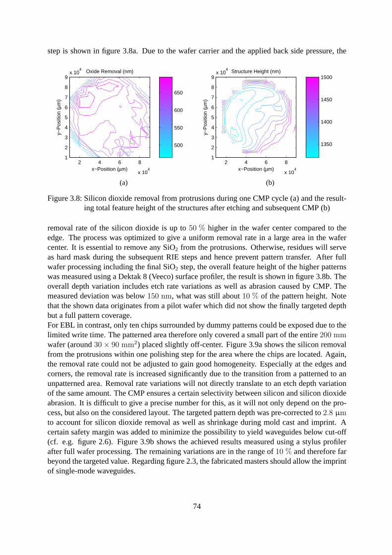
step is shown in figure3.8a. Due to the wafer carrier and the applied back side pressure,the
x−Position (µm)
y−P
ositi
on (µ
m)
Oxide Removal (nm)
2 4 6 8
x 104
1
2
3
4
5
6
7
8
9x 10
4
500
550
600
650
(a)
x−Position (µm)
y−P
ositi
on (µ
m)
Structure Height (nm)
2 4 6 8
x 104
1
2
3
4
5
6
7
8
9x 10
4
1350
1400
1450
1500
(b)
Figure 3.8: Silicon dioxide removal from protrusions during oneCMP cycle(a) and the result-ing total feature height of the structures after etching andsubsequentCMP (b)
removal rate of the silicon dioxide is up to50 % higher in the wafer center compared to theedge. The process was optimized to give a uniform removal rate in a large area in the wafercenter. It is essential to remove any SiO2 from the protrusions. Otherwise, residues will serveas hard mask during the subsequentRIE steps and hence prevent pattern transfer. After fullwafer processing including the final SiO2 step, the overall feature height of the higher patternswas measured using a Dektak 8 (Veeco) surface profiler, the result is shown in figure3.8b. Theoverall depth variation includes etch rate variations as well as abrasion caused byCMP. Themeasured deviation was below150 nm, what was still about10 % of the pattern height. Notethat the shown data originates from a pilot wafer which did not show the finally targeted depthbut a full pattern coverage.ForEBL in contrast, only ten chips surrounded by dummy patterns could be exposed due to thelimited write time. The patterned area therefore only covered a small part of the entire200 mmwafer (around30× 90 mm2) placed slightly off-center. Figure3.9ashows the silicon removalfrom the protrusions within one polishing step for the area where the chips are located. Again,the removal rate could not be adjusted to gain good homogeneity. Especially at the edges andcorners, the removal rate is increased significantly due to the transition from a patterned to anunpatterned area. Removal rate variations will not directlytranslate to an etch depth variationof the same amount. TheCMP ensures a certain selectivity between silicon and silicon dioxideabrasion. It is difficult to give a precise number for this, asit will not only depend on the pro-cess, but also on the considered layout. The targeted pattern depth was pre-corrected to2.8 µmto account for silicon dioxide removal as well as shrinkage during mold cast and imprint. Acertain safety margin was added to minimize the possibilityto yield waveguides below cut-off(cf. e.g. figure2.6). Figure3.9bshows the achieved results measured using a stylus profilerafter full wafer processing. The remaining variations are in the range of10 % and therefore farbeyond the targeted value. Regarding figure2.3, the fabricated masters should allow the imprintof single-mode waveguides.
74

x−Position (µm)
y−P
ositi
on (
µm)
Oxide Removal (nm)
−4 −2 0 2 4
x 104
0
2
4
x 104
750
800
850
900
950
1000
1050
(a)
x−Position (µm)
y−P
ositi
on (
µm)
Feature Height (nm)
−4 −2 0 2 4
x 104
0
2
4
x 104
2300
2400
2500
2600
2700
(b)
Figure 3.9: Silicon dioxide removal from elevated structures during oneCMP cycle(a) and theresulting total feature height of the patterns after etching and subsequentCMP (b)
3.2.4 Reactive Ion Etching
For all results shown within this work, a continuous siliconreactive ion etching (RIE)pro-cess, similar to the one described previously [72], was performed. For all100 mm wafers, anAdvanced Silicon Etch System (Surface Technology Systems)was used. Due to limited wafersize, the process had to be transfered and optimized on a Pegasus (Surface Technology Systems)etch system for200 mm wafers. Both systems include a helium backside cooling to stabilizethe wafer temperature during etch and avoid the rapid degradation of the used resist masks. Tobe able to run several etch tests with one resist exposure, pilot wafers were cleaved into sam-ples and etched thereafter. To ensure an improved thermal contact to the substrate, heat transferpaste was used to place the samples onto a dummy wafer.
TaperMain foci of the optimization of the etch process were sufficient selectivity, a negligible un-dercut and minimal roughness at the pattern sidewalls as well as at the trench bottom. Figure3.10ashows the results obtained with the standard process using the Advanced Silicon Etch(ASE) System. Herein, a resist taper as well as a sidewall inclination within the trench canbe observed. Figure3.10bdepicts the measured top and bottom width against their respectivetarget values for dense and isolated trenches. In the considered range of dimensions, a constantoffset of roughly110 nm can be observed. For a homogeneous etch depth of960 nm as presentin this etch test, this is equivalent to a constant sidewall angle of86.0 to 86.5◦. Considering acompletely anisotropic etch process, a selectivity of 5 anda measured resist sidewall angle of81◦, one would expect a taper of the silicon structures larger than88◦. The difference betweenthis value and the measured86◦ can be traced back to the anisotropy of the usedRIE process.During the process optimization on the200 mm EBL wafers using the Pegasus etch system,the selectivity of the etch process could be enhanced to8. Moreover, it was easier to achievestraight sidewalls instead of a certain inclination angle.Optimization would have required more
75

(a)
0 100 200 300 400 500 6000
100
200
300
400
500
600
700
800
Design CD (nm)
Measure
d C
D (
nm
)
0 100 200 300 400 500 6000
100
200
300
400
500
600
700
800
Design CD (nm)
Measure
d C
D (
nm
)
wt dense
wt iso
wb dense
wb iso
wt
wb
(b)
Figure 3.10: Scanning electron micrograph showing a cross-section of an etched silicon struc-ture exhibiting a tapered sidewall in the resist as well as inthe final silicon structure(a)and the measured trench widths at the top and the bottom of thesilicon features(b)
test-samples with the target layout. Unfortunately, thesewere not available. Both, high selectiv-ity as well as high etch anisotropy are usually desirable. Unfortunately, the sidewall angle wassteeper than the one used for etch-bias calculation during process planning. Thus, the wave-guides of the final mold showed smaller lateral dimensions and theMRR gaps were broadenedconsiderably.
Etch depth homogeneityPattern height variations are not only generated byCMP abrasion, but also caused by etch ratevariations duringRIE. Etch depth variations may not only depend on the pattern dimensions (cf.section2.3.3), but can also occur on wafer scale. The etch process is influenced by all processparameters like plasma power, gas flow, temperature as well as pressure. These will usuallyvary over the wafer and are strongly effected by the design ofthe etch chamber [109].Figure3.11shows the etch depth of the second patterning layer, i.e. thecoupler grating. Theachieved etch depth was measured again using a stylus profiler on large test patterns. As the etchrate also depends on the feature size, further deviations may be present at the coupler gratings.Herein the homogeneity over the100 mm wafer is below35 nm, but slightly off the target valueof 407 nm. However, the coupler efficiency is much more effected by an etch depth which is toolarge than one being too small. A reducedAR caused by the lower etch depth further reducesthe possibility of pattern damage during demolding. The deviations remain relatively low in thewafer center and are pronounced at the edge. They may be caused by field inhomogeneities inthe etch chamber.
Etch defectsDespite of careful pilot tests and optimization, some problems occurred during the final siliconRIE andCMP. Figure3.12adisplays a first order reflector within a waveguide. The micrograph
76

x−Position (µm)
y−P
ositi
on (µ
m)
Etch Depth (nm)
Dep
th (
nm)
2 4 6 8
x 104
1
2
3
4
5
6
7
8
9x 10
4
360
365
370
375
380
385
390
395
Figure 3.11: Depth variations of the low etch depth (gratingcoupler) throughout a100 mmwafer patterned using a wafer stepper
(a) (b)
Figure 3.12: Two types of defects in the silicon master: caused by an undercut during etchobserved before resist removal(a)and due to resist collapse prior to etch observedafter full processing(b)
shows an etch-test at which the resist was still present. Thefinal wafers patterned withEBLmost likely showed similar results but could not be observedusing theSEM due to the wafersize and the necessity to deposit a conductive film. Two factors are responsible for the obtainedresults. The etch bias was set to69 nm as mentioned above. The first order reflector was notexcluded from this correction and hence165 nm resist lines had to be patterned. Furthermore,the etch process produced a local undercut. Local depletionof polymer builders due to theincreased sidewall density may have caused this issue.Figure3.12bdisplays the results for the first order reflector after full processing, including twolithography, one polishing and two etch steps. The patternscould not be fabricated successfully.Most likely, the failure mechanism was different from the one of the etch defect described sofar. The patterns show a pitch doubling or tripling. This indicates the collapse of the resist linesprior to etch. Similar to the results shown in figure3.15, theAR of the patterns may have beenresponsible for this kind of defect.
77
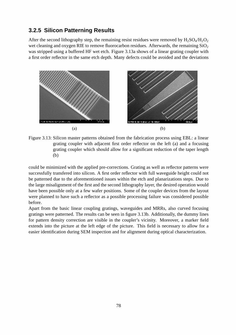
3.2.5 Silicon Patterning Results
After the second lithography step, the remaining resist residues were removed by H2SO4/H2O2
wet cleaning and oxygenRIE to remove fluorocarbon residues. Afterwards, the remainingSiO2
was stripped using a buffered HF wet etch. Figure3.13ashows of a linear grating coupler witha first order reflector in the same etch depth. Many defects could be avoided and the deviations
(a) (b)
Figure 3.13: Silicon master patterns obtained from the fabrication process usingEBL: a lineargrating coupler with adjacent first order reflector on the left (a) and a focusinggrating coupler which should allow for a significant reduction of the taper length(b)
could be minimized with the applied pre-corrections. Grating as well as reflector patterns weresuccessfully transfered into silicon. A first order reflector with full waveguide height could notbe patterned due to the aforementioned issues within the etch and planarizations steps. Due tothe large misalignment of the first and the second lithography layer, the desired operation wouldhave been possible only at a few wafer positions. Some of the coupler devices from the layoutwere planned to have such a reflector as a possible processingfailure was considered possiblebefore.Apart from the basic linear coupling gratings, waveguides and MRRs, also curved focusinggratings were patterned. The results can be seen in figure3.13b. Additionally, the dummy linesfor pattern density correction are visible in the coupler’svicinity. Moreover, a marker fieldextends into the picture at the left edge of the picture. Thisfield is necessary to allow for aeasier identification duringSEMinspection and for alignment during optical characterization.
78

3.3 Polymer Mold Fabrication
The fabricated silicon masters obtained from the work presented in section3.2cannot directlyserve as imprint mold. Firstly, they are not UV-transparent. This would either limit their appli-cation to thermoplastic resists or to a through substrate exposure usingUV-NIL . Secondly, thefabricated waveguides, couplers andMRRsare present in their positive tone within the master,which was shown to be advantageous for fabrication. As the patterns should appear in polymerafter imprint in the same tone, an inverted working mold has to be cast from the silicon mas-ters before imprint. Apart from other materials, polymers are potential candidates to serve as aworking mold material. Section2.4 mentioned some of the inherent features and possibilitiesoffered by them.In the following, the results of the polymer mold productionare summarized. To be able todecide for a suitable mold material, a overview of differentcommercially available options isgiven first. The materials are also analyzed regarding theirmechanical stability within exper-iments. The results are compared with the theoretical predictions based on the considerationsgiven in section2.4.3.2. Afterwards, the detailed process flow for the production ofpolymermolds for stamp-and-repeat patterning is given. The obtained results are discussed with respectto their impact on the imprint process. An alternative stampgeometry as well as the resultsobtained with the same is presented in the end.
3.3.1 Possible Materials for Polymer Molds
During the recent decades, many publications dealt withPDMS as a mold material for soft-lithography. Most likely this is due to the facts that it is easy to handle and cheap. Furthermore,due to its mechanical and chemical properties, it neither requires sophisticated equipment forprocessing nor imprinting. During the past few years, first commercially available imprint sys-tems have commonly usedPDMSstamps. Most notably, the surface conformal imprint lithog-raphy (SCIL) tools of Süss Microtec [153] were established. However, material parameters ofPDMSinhibit the extension ofNIL to the patterning of arbitrary layouts. These might requiresqueezed resist flow or highAR, e.g. for the direct patterning of functional elements. Theprinciple goal is to have polymers which are easy to handle but still show a high mechanicalstrength as well as a lowSFEand are most likely sub i-line UV-transparent. Easy handlingmostly includes that they can be applied in a low viscous form, which can be changed to a solidstate later on. Much research has been done to improve the mechanical stability of siloxane-based polymers. H-PDMSand X-PDMSare used frequently, unless their Young’s modulus stillremains at values of8− 12 MPa and65− 80 MPa, respectively [153, 154]. Another materialclass are Teflon-likeperfluoro-polyether-urethane-dimethacrylates (PFPEs)[155, 156]. Table3.1summarizes potential mold materials and theirUV-NIL -related properties.
Additionally to the already mentioned materials, hybrid polymers [132] and polyurethaneacrylate (PUA)based resins are included, which show a comparably high Young’s modulus.Unless stated otherwise, the data given in table3.1was measured within this work. It was alsopartly published within a journal paper [140]. Contact angles were measured using acetone,isopropyl alcohol and water on flat spun-on surfaces of the used mold materials with a con-tact angle measurement system OCA 10 (DataPhysics Instruments). With the measured values,
79

Table 3.1: Material properties of commercial soft mold polymers
Name Typ Young’s SFE Eγ
Trans- Vendormodulus parency
cut-off(MPa) ⋆ (mN/m) (mm−1) (nm)
Sylgard 184 PDMS 4 25 0.16 ≈ 300 ** Dow ChemicalFomblin MD 40 PFPE 31 13 2.4 ≈ 400 ** Solvay SolexisFluorolink MD 700 PFPE 120 15 8 ≈ 400 ** Solvay SolexisOrmostamp RXP Ormocer 1100 41 27 ≈ 320† Microresist
11 * 100 * TechnologyMINS 311 RM PUA 920 20 46 < 365‡ Minuta
Technology⋆ at room temperature.* with appliedF13-TCS ASL. ** [157]. † [134]. ‡ [158].
the surface energies of the materials were calculated usingthe Owens-Wendt-Rabel-Kaelblealgorithm [159]. Data on the mechanical behavior of the materials was obtained from nano-indentation measurements on polymer films in collaborationwith the Fraunhofer Institute forNondestructive Testing IZFP. All samples were tested with the same measurement setup andprocedure to ensure comparability.The given materials are a selection of a much wider range of possibilities. Alternatively, e.g.polyvinylsilazane (PVSZ) [160, 161] or even hydrogen silsesquioxane (HSQ) [110, 162] maybe used as mold materials. In the following, cleaning defects occurring on highAR patterns arediscussed in detail.
Cleaning DefectsA validation of the theoretical models concerning pattern collapse on a mold during cleaning,which were collected in section2.4.3.2, is desirable. Experiments were performed with someof the commercially available materials listed in table3.1. Stability depends on the lateral di-mensions and theAR of the considered patterns. Gratings and pillar arrays werechosen as testobjects as they are relevant for the replication of photonicstructures in general, also includinggrating couplers. The results presented in the following are partly enclosed in a publication[140].Silicon master structures were fabricated with a process similar to the one described in section3.2. First, a wafer stepper exposure of a resist using an ASML PAS5500-250 C was performed.The customized layout contained line-space gratings with pitches of600− 2000 nm as wellas dot arrays in a quadratic lattice and diameters of500− 2000 nm with variousduty cycles(DCs). The patterned resist layers were used as etch-masks forRIE to gain different etch depthsranging from500 nm to 3200 nm. After resist stripping, aF13-TCS ASL was applied to thesilicon molds by means of molecular vapor deposition.Polymer molds were cast from the silicon masters usingFluorolink MD 700 (Solvay Solexis)(MD 700) andFomblin MD 40 (Solvay Solexis) (MD 40), both with2 wt % 2-hydroxy-2-me-thylpropiophenone (Sigma-Aldrich) as a photoinitiator, as well as Ormostamp (MRT). Glass
80

slides were used as substrates. APS1 (MRT) was used as adhesion promoter forMD 40 andMD 700 as well as OrmoPrime08 (MRT) for Ormostamp. All materials were manually dis-pensed onto the silicon masters and subsequently brought into contact with the substrates usingthe customized imprint press. The material was cured using aUV-LED (Nichia NC4U133) un-der a nitrogen atmosphere. A thick residual layer in the order of several10 µm was present inevery polymer mold cast.The stability against collapse was tested using several cleaning agents. These had to be able tosolve uncured resist residuals and to flush particles away. Furthermore, they should not swell ordissolve the mold material or parts of it. All molds were flushed with isopropyl alcohol directlyafter demolding from the silicon master and subsequently dried using a nitrogen stream. Duringthe experiments, other cleaning agents (acetone, ethanol and deionized water) were also used.They show different contact angles to the used mold material. Therefore, the structures affectedby feature collapse after cleaning varied. In the following, all results are shown for isopropylalcohol cleaning for the sake of clarity.
In order to model the behavior of the structures according tothe equations given in section2.4.3.2, some material parameters are necessary, they are given in table3.1. Additionally, thePoisson’s ratioν was assumed to be0.3 for all considered materials.First of all, the measured stability behavior of pillars with different diameter is given in figure3.14a. For the simulation of the lateral collapse half-pitch structures (Λ = 2d) were assumed.
400 600 800 1000 1200 1400 16000
2
4
6
8
10
Pillar Diameter (nm)
Asp
ect R
atio
Fomblin MD 40
ground collapselateral collapse
(a) (b) (c)
Figure 3.14: Critical aspect ratio for different pillar diameters with measured values (o = un-stable, x = stable) and simulation results(a), instable patterns (diameter500 nm,height3.1 µm) (b) as well as stable patterns (diameter1000 nm, height3.1 µm)(c) (materialMD 40)
In general, the failure mechanism depends on the dimensionsof the features. Below the criticalAR of lateral collapse, most considered features are stable and therefore no feature collapsewill occur as visible in figure3.14c. In the area between the criticalAR of lateral collapse andground collapse, only lateral collapse will be present. Dense features tend to collapse in thisarea, whereas isolated features are still stable. If theAR is increased further, the ground collapsecriterion is reached and isolated features will become unstable. Both failure mechanisms can be
81

observed for highAR features, as depicted in figure3.14b, showing a boundary of a pillar array.Posts at the edge (lower part of figure3.14b) show a ground collapse, whereas those in the arraycenter are subject to lateral collapse. Due to process limitations, it was only possible to fabricatea limited set of sample features. The results are only able toshow qualitative agreement betweenthe experiments and theory. In conclusion, the criticalAR for MD 40 is limited to3− 4 in theconsidered range of dimensions but depends on the feature size.
A comparison of the simulation results for grating patterns, based on the theory shown insection2.4.3.2and the experiments, can be obtained from figure3.15a. This shows good agree-ment for pitches around750 nm but deviations for larger ones. Examples of collapsed and stablegratings are given in figures3.15band3.15c, respectively. During silicon master fabrication,
500 1000 1500 20000
1
2
3
4
5
6
7
8
Grating Pitch (nm)
Asp
ect R
atio
Fluorolink MD 700
(a) (b) (c)
Figure 3.15: Critical aspect ratio for different grating pitches based on simulation with mea-sured values (o = unstable, x = stable)(a), instable patterns (pitch800 nm, height3.1 µm) (b) as well as stable patterns (pitch1800 nm, height3.1 µm) (c) (materialMD 700)
the duty cycle of the resist features differed from the design value of0.5 but was reproduciblefor different structure heights. All simulation results shown took the real dimensions of the fea-tures measured by scanning electron microscopy into account. It is visible from the simulationas well as from the experiments that the achievableAR depends on the pitch of the dense struc-tures. This also holds true assuming perfect half-pitch structures. Residual deviations in figure3.15amight be explained by a sidewall angle differing from90◦. TheSFEof the cast structuresmight also be different to the spun-on films, where the contact angles were measured. TheSFEof a master can influence theSFEof a cast mold [163].
Figure3.16ashows the criticalAR depending on the grating pitch for different mold mate-rials. The subfigures3.16b,3.16cand3.16dexhibit mold structures cast from the same masterin different materials. Herein, only Ormostamp is able to withstand a cleaning procedure withisopropyl alcohol without feature collapse. TheSFEof untreated Ormostamp is higher than thatof MD 40 andMD 700 (cf. table3.1), resulting in smaller contact angles respectively. Conse-quently, higher pressure differences between adjacent capillaries Eq.(2.30) are generated. Thehigher Young’s modulus is able to compensate this rise completely.
82

500 1000 1500 20000
1
2
3
4
5
6
7
8
Pitch (nm)
Aspect R
atio
Ormostamp
MD 700
MD 40
(a)
(b) (c) (d)
Figure 3.16: CriticalARs for different pitches and materials based on simulation(a)where (×)denotes the dimensions of the structures in the experiment either made ofMD 40(b) MD 700 (c)or untreated Ormostamp(d) all cast from the same master
The dependence of the criticalAR on the Young’s modulus of the mold material is givenin figure 3.17. The slope is much steeper in the region of a low Young’s modulus, where
0 200 400 600 8000
1
2
3
4
5
6
7
Young‘s Modulus (MPa)
Max
imal
Asp
ect R
atio
Figure 3.17: Critical aspect ratio for different Young’s moduli (structures: half-pitch300 nm,sidewall angle90◦, surface energy41 mN/m, isopropyl alcohol cleaning)
materials likePDMS or PFPEcan be found. Stiffer materials, like Ormocers orPUAs, can
83

drastically increase the criticalAR. Although the elastic modulus has a major effect on thestability of polymer mold patterns, the stability can also be tuned by the surface properties ofthe mold material. Usually, the application of anASL will lower the SFE. However, solventslike isopropyl alcohol or acetone do show a wetting behavior(contact angle45− 60◦) even onsurfaces with very low surface energy, like those with applied F13-TCS layers. Therefore, itis difficult to eliminate the capillary meniscus forces by increasing the contact angle to90◦ orabove by changing the solvent.
Best Suited MaterialThe former considerations suggest that the decision in favor of a polymer mold material is easy.The main parameters to be considered are the Young’s modulus, which should be as high aspossible and theSFE, which should stay as low as possible. The general trend is ofcoursetrue, but for a specific pattern and technology, the decisionmight not be that easy. As alreadydiscussed, theSFEis not able to describe all possible surface interactions. Therefore, the moldmaterial as well as an additionally appliedASL have to be compatible with the resist used.Furthermore, the stiffer the mold, the lower is its ability to account for planarity differences tothe substrate and particles. This drives the demands on the master, the imprint equipment as wellas the cleanroom environment. The combination of MINS 311 RM as a mold and Ormocore asa resist seems to be promising.
84

3.3.2 Bonded Mesa Structures
The goal of step-and-repeat imprinting is to repeatedly replicate a single chip on a wafer. A chip-sized mold is necessary for this purpose. In reality, the basic approach shown in figure2.36hasto be extended, to yield a mold compliant with the restrictions imposed by the process and theused equipment. Conventionally, fused silica molds are usedas templates, where a mesa pro-trusion defines the active imprint area. This mesa can be patterned from a bulk template eitherby etching or milling the surrounding area of the template. The active mold area can either pre-viously or afterwards be patterned using the techniques described in section2.3. However, dueto the unconventional substrate size (usually65× 65× 6.35 mm3), a full processing of such amold is difficult, as most of the equipment within semiconductor manufacturing is dedicatedto wafers of different sizes. One way to circumvent this issue is to use a bonded mesa pattern.This can be a chip which was previously fabricated within a full wafer and subsequently dicedto the size desired. Previous works at theIHM have focused on a process to bond a patternedmesa adhesively to a template [9, 164]. Therein, possible adhesives were investigated regardingbond joint strength, achievable planarity and chemical stability. The results are the basis forthe process scheme followed to produce a polymer mold imprint template as depicted in figure3.18. In contrast to previous works, a flat mesa is used to give a constrained area replicated
VI. Imprint
Substrate Imprintmaster Anti-Sticking Layer
Resist
V. Anti-Sticking-Layer Deposition
Fused Silica Polymer Mold
IV. Working Stamp Cast
III. Adhesion Promoter DepositionII. Mesastructure BondingI. Template Preparation
Adhesion Promoter
Adhesive
Figure 3.18: Production scheme of polymer molds for step-and-repeat imprint using fused silicatemplates with bonded mesa structure
later on. For all results shown, Katiobond 4670 (DELO) was used as an adhesive, which wasmanually dispensed to the template. Depending on the requirements, the mesa was afterwardsplaced using the NPS 300, which is a dedicated flip-chip bonder, or manually. For the latter,the adhesive spread under the mesa due to capillary forces, whereas an external force could beapplied using the NPS 300. In any case, part of the bond adhesive will form a meniscus at theedges of the mesa. Subsequently, the adhesive was UV-cured either using the UV-LED arrayinside the NPS 300 or a customized UV-LED.Before a polymer mold can be cast, usually a specific adhesion promoter has to be applied.In most cases, commercially available mold polymers come with a promoter suitable for glasssubstrates. Based on the results shown above, Ormostamp and MINS 311 RM are most suit-able for the targeted application. The respective adhesionpromoters Ormoprime 08 (MRT) andPUA Glass Primer (Minuta Tech.) have to be applied via spin-coating and baked subsequently.Edge bead formation is an inherent problem to spin-coating.For Ormoprime 08 a large edgebead formation could be observed. The issue was less critical to the PUA Glass Primer. An
85

edge bead hinders the minimization of the polymer mold thickness which is beneficial to in-crease the template’s stiffness (cf. section2.4). To circumvent any edge bead, an adhesionpromoter can be applied from the gas phase. Both, Ormostamp and MINS 311 RM are acrylate-based, which enables the deposition of a siliane-based adhesion promoter with a similar setupas used forASL application. (3-methacryloxypropyl)-trichlorosilane (TCS-MA)(AB109004,abcr GmbH & Co. KG) is a well-known adhesion promotor for acrylic resins [9]. It was usedand showed sufficient adhesion to avoid mold detachment fromthe template. If the polymerthickness should not be minimized, spin-coating the adhesion promoter is sufficient. After ap-plying the adhesion promoter, the mold could be cast from themaster with appliedASL. Forthis purpose the mold polymer was manually dispensed on the master. If a precise alignmentwas not required, the fabricated template could be placed atop manually as well. Capillaryforces and the self-weight of the template spread the polymer over the entire area before it wascured using the customized UV-LED. Alternatively, the NPS 300 could be utilized to place andalign the mesa with respect to the master. In principle, an alignment accuracy of< 500 nm canbe achieved. The template was then brought into contact withthe master. Damage to the mastershould be avoided by a minimal pressure. The NPS 300 can control the applied pressure duringimprint or mold casting. Practical experiments have shown,that the minimal controllable forceis≈ 5 N. This results in an imprint pressure of already0.02− 0.05 MPa depending on the chipsize. Ormostamp and MINS 311 RM show viscosities, which will lead to thin polymer layersafter casting. Therewith, the possibility of master damage, due to particles or template contactis increased. Particle contaminations of the template including mesa cannot be excluded due tomanual handling. Unfortunately, the possibilities to clean the template are limited. As in theentire process, the equipment available for cleaning is mostly dedicated to wafers and requiresspecial tooling for the used template sizes. Furthermore, the used bonding adhesive (Katiobond4670) is an epoxy-based resin and is not able to withstand aggressive cleaning procedures, e.g.with H2SO4/H2O2 [9]. The polymer mold can be cured using the UV-LED array of the NPS 300.An nitrogen or helium purge avoided oxygen inhibition during mold curing.Demolding mostly has to be performed manually. The NPS 300 allows automated demoldingand can further measure the force required for this. Unfortunately, the chuck vacuum is not ableto hold the master due to its small area (cf. section3.2). For manual demolding, precautionshave to be taken to avoid shear forces or a peel-demolding. Many pattern defects could be elim-inated by proper demolding. For this purpose, an automated demolding process, which involvesforces vertical to the surface only, is desirable. This is possible if the unpatterned area aroundthe active chip of the master is increased.The MINS 311 RM polymer mold can be used for imprint straight away. For Ormocore, theapplication of an additionalASL is necessary. For this purpose,F13-TCSwas applied with thecustomizedMVD setup after surface hydroxylation using an oxygen plasma was performedwithin a Plasmalab 80 PLUS (Oxford Instruments).
86

3.3.3 Flatness of Polymer Molds
A polymer mold resembles the patterns of the master it was cast from. A mold as fabricated in3.2will not only show the pattern deviations as already discussed. Additionally, it will show asurface which is not perfectly flat. In theory, mold and substrate are often considered as per-fectly flat, which would lead to a simultaneous contact of theentire imprint area, if tilt errors areexcluded. In reality, neither the mold nor the substrate surface are perfectly flat. Figure3.19ashows the deviations from an ideal flat surface of the siliconmaster. The data was obtainedusing a customized confocal microscope PLµ 2300 (Sensofar-Tech). It includes a precisionthree-axis stage as well as a10x phase-shift objective. This combination allowed the acquisi-tion and stitching of> 100 in-die topography images, as required to cover the entire mold area,within a reasonable measurement time. The acquisition of the necessary topography data is
-0.5 0 0.5
Flatness Error (µm)
2 4 6 8 10 12
2
4
6
8
10
12
x−Position (mm)
y−P
ositi
on (
mm
)
(a)
2 4 6 8 10 12
2
4
6
8
10
12
x−Position (mm)
y−P
ositi
on (
mm
)
(b)
Figure 3.19: Flatness deviation of a silicon master chip(a) and the same for aPUA polymermold cast from it(b)
rather difficult, as the master surface is patterned. The lateral pattern dimensions are mainly inthe range of5 µm, as dummy patterns dominate the given layout as visible in figure3.2. It istherefore possible to use a low magnification system, while still be able to distinguish betweentrenches and protrusions. When the structures become smaller, the resolution of the system,hence the magnification of the objective, has to be changed. This will lead to drastically in-creased measurement times. Complex layouts may generate artifacts as visible in figure3.19.The flatness inhomogeneity of the silicon master is roughly±500 nm. As visible in figure3.19b, the inhomogeneity also transfers to a polymer mold cast. Contact of the mold and asubstrate occurs in the center region during imprint. Depending on the stiffness of the mold andthe substrate, the applied imprint pressure leads to a deformation of the mold and, hence, a con-formal contact. If the applied pressure is low, which is desirable to avoid feature deformation,conformal contact may not be achievable within the entire mold area. This is especially true ifthe complete mold stack involves stiff materials.Planarization or cushion sheets can be integrated into the imprint stack to account for this prob-lem [165–167]. For most of the results shown within this thesis, aPDMS cushion layer was
87

inserted directly underneath the substrate.
3.3.4 Polymer Molds using Flexible Mesa Structures
Reducing the effect of the mold flatness inhomogeneity by introducing a cushion layer under-neath the substrate induces serious issues for step-and-repeat imprinting. If a chip-sized moldis pressed onto a substrate with a flexible backbone, the substrate will be locally deformed.Depending on the cushion layer’s thickness, imprint pressure and chips size, the substrate mayalso break due to load jumps at the mold edges. A more general way is the integration of acushion layer within the mold. Figure3.20shows a comparison of a polymer mold with rigidand flexible backbone. The one with the rigid backbone can be produced according to the pro-cess shown in figure3.18. Integration of a flexible backbone can follow a similar route. Here,the fused silica mesa structure is exchanged with a softer material. For the experiments shownin the following,PDMSwas cast directly on a silica template using a mold with a pre-definedgroove with a depth of roughly500 µm. Subsequently, an oxygen plasma treatment using aPlasmaLab 80plus (Oxford Instruments) was performed. Mostof the commercially availableadhesion promoters dedicated to silica surfaces can be applied further on, as the oxygen plasmagenerates reactive hydroxyl groups on the siloxane backbone ofPDMS.Figure3.21ashows the imprint results obtained using a mold with flexiblemesa and aPUA
Working Stamp Polymer
Fused Silica Adhesion Promoter
Rigid Backbone
PDMSAdhesive
Flexible Backbone
Figure 3.20: Comparison of a molds with a fused silica template and a flexiblePDMSor a rigidfused silica backbone
working stamp polymer. Conformal contact was reached over the total chip area in conjunc-tion with no visible defects resulting from incomplete filling. Unfortunately, theRLT showed alarge variation of±220 nm as visible in figure3.21a. By comparison of theRLT results and thelayout shown in figure3.2, it is visible that resist will remain in sparsely patternedareas. Theresidual resist is accumulated at the end of the line-shapeddummy features.As already discussed, the given layout includes large unpatterned areas and requires a squeezedflow of the resist. The flow within a cavity will depend on the pressure difference applied(cf. eq. (2.27)). If the Young’s modulus of the backbone material is low (≈ 4 MPa), largerdeflections are necessary to achieve the same pressure difference as for a silica mesa (Young’modulus≈ 70 GPa). Reducing the initial film thickness lowered the maximumRLT thicknessbut the relative variation remained high. As theRLT is of crucial importance for the gratingcoupler’s performance (cf. section2.2.2), this variation is not tolerable. For comparison, figure3.21bshows the results obtained using a rigid backbone with the other processing conditionsremaining the same as before.RLT variations of only±23 nm were measured in the area underconsideration and can be mainly addressed to pattern heightinhomogeneities as will be dis-cussed later on.
88

0 100 200 300 400 500
Residual Layer Thickness (nm)
0 1 2 3 4 50
1
2
3
4
5
x−Position (mm)
y−P
ositi
on (
mm
)
(a)
0 1 2 3 4 50
1
2
3
4
5
x−Position (mm)
y−P
ositi
on (
mm
)
(b)
Figure 3.21:RLT inhomogeneity induced by different stamp stacks using aPUA (MINS 311RM (Minuta Tech.)) mold material with a flexible backbone(a) and a rigid back-bone(b) (initial resist thickness approx.845 nm, imprint pressure0.01 MPa, hold-ing time600 s)
The integration of a flexible layer which is able to account for flatness deviation of the moldis desirable. A stack including a polymer mold in combination with a fused silica mesa and aPDMS layer underneath may be an opportunity. Also, the thicknessof the polymer workingmold will have an influence as long as its Young’s modulus is not in the range of the used silicamesa.
89

3.4 Imprint
3.4.1 Imprint Setup
Imprint experiments within this thesis were performed using two imprint setups. One is a step-and-repeat imprint system operated in theIPMS cleanroom.T-NIL andUV-NIL are possiblebut require different imprint heads. The system can performimprints on wafers up to200 mmdiameter, including alignment as well as automated tilt correction between mold and substrate.The process can be fully automated to perform all imprints within a wafer, whereas no waferhandling system is included. Conventionally,65× 65 mm2 mold templates with a thicknessof 6.35 mm are used forUV-NIL . As described in the previous section, the fabrication of aworking mold on top of a template includes several process steps (cf. figure3.18). Most ofthem require several iterations of optimization. The preparation of such templates and their usewithin the NPS 300 is a rather difficult task due to the requirements imposed by the machine.To account for this, a customizedUV-NIL imprint press was designed and built within thisthesis; it is located atIHM. Pressure can be applied manually and measured. A rather simpletilt compensation as well as alignment are also possible on wafers up to100 mm or samples. Ifneeded, the system can be additionally purged using He or N2 to prevent oxygen scavenging.The simple setup allowed for a quick and easy evaluation of the desired processes in a laboratoryenvironment.
3.4.2 Reverse Imprint
Conventionally, the resist is applied to the substrate on which the imprint should be performed.Alternatively, the resist can also be applied to the stamp, what is often called reverse imprint[34]. During the experiments of a project [151, 168], it was observed that a reverse imprintcan avoid the imprint-inherent residual layer by guided dewetting. The work presented in thefollowing was conducted in collaboration with René Hensel and is part of a publication [150].The silicon molds used in the following were fabricated using projection lithography andRIE,similar to the one presented in section3.2.2. Originally, the silicon masters were targeted asmolds for thermal imprint and hence showed a negative tone ofthe waveguide features. Un-fortunately, silicon molds cannot be used for standard through-moldUV-NIL exposure as theyare not transparent for UV radiation. In principle, they canbe used in a through-substrateexposure system which is impossible as silicon substrates with a silicon dioxide cladding areused. In contrast, polymer working stamps can allow a through-mold exposure. For replication,15× 15 mm2 large chips were diced from the wafer master. Polymer molds were cast fromthe silicon master using UV-curablePFPE(Fluorolink MD 700, Solvay Solexis) with0.5 wt%of 2-hydroxy-2-methylpropiophenone (Sigma-Aldrich) as aphotoinitiator. The whole processflow for the structure replication is depicted in figure3.22. For tone inversion, a secondPFPEmold was cast from the daughter mold without adding any releasing agent. A low viscous liquidpoly(ethylene-glycol)-diacrylate (PEG)(700 g/mol, Sigma-Aldrich) solution with0.5 wt% ofa benzophenone photoinitiator (Irgacure 651, CIBA) was applied to the patternedPFPEby dip-coating using a LB Dipping System LD 1 (Riegler and Kirsten). The entire secondPFPEmoldwas dipped into the resist and subsequently withdrawn usinga constant velocity of0.3 mm/s.
90

II. Tone InversionI. Mold Casting III. Resist Dipcoat
IV. Resist Curing V. Demolding
Silicon PEGdaPFPEdma
Figure 3.22: Process flow for the double daughter mold casting for tone inversion and the resid-ual layer free reverse imprint
During withdrawal, the meniscus of the resist solution is moved along the patterned surface.No resist solution was deposited at the elevated flat regionsatop the mold due to the low sur-face energy of thePFPEmaterial (15− 16 mN/m) and a consequent receding contact angle of51± 2◦ was measured by a Contact Angle System OCA 30 (Dataphysics), being in agreementwith earlier reports on capillary assembly [169]. However, the features (channels, grooves)were filled with resist due to capillary forces [170]. The trenches act as pinning barriers againstthe advancing meniscus which was first deformed and subsequently disrupted without leavingthe patterns depleted. Silicon substrates were used for thesubsequent reverseUV-NIL process.TCS-MA was deposited as a coupling agent using vapor phase deposition. ThePFPEmold wasbrought into contact with this silicon substrate and a curing process was induced by LED UVirradiation (365 nm, 720 J/cm2) in the customized imprint tool with a nitrogen atmosphere.Across-sectional view of the obtained results is depicted infigure3.23a. Features with differentheight levels and no residual layer between the features could be transfered. The process flow
(a)
20 µm
(b)
Figure 3.23: Residual layer free polymer patterns with two height levels on a silicon substrateshown in a cross-section(a)and resist bridging within a ring-shaped trench(b)
presented was able to achieve acceptable results for multiple kinds of repetitive features likegratings or dot arrays. However, residual layer free replication of more complex shapes turnedout to be difficult. The set of possible dip-coating parameters is restricted by the rotation of themold, the angle of the mold to the resist surface and the withdrawal velocity. These have to be
91

optimized for each combination of mold and resist material.Optical properties of the imprintresist are of overriding importance to maintain a efficient device operation. Hence, the choiceof possible material is further reduced. Despite of an optimized process, some patterns do showbridging effects between adjacent trenches as depicted in figure3.23b. Here, the inner part ofthe ring is completely covered with resist, which will consequently yield a residual layer in thisarea. For some pattern geometries, the bridging state may beenergetically favorable comparedto a dewetted state. Furthermore, the energy barrier to change the states might also be highenough to make a change rather unlikely.As theRLT has a significant impact on the performance of theMRR and the grating couplers,the presented method might be a technological option in the future.
3.4.3 Direct Pattering of Spin-coated Films
The NPS 300 provides a drop-on-demand dispensing unit. As already discussed, many prob-lems occurring inNIL can be diminished if the initial resist height can be locallyadjusted.Ormocore is not a dedicated material for drop-on-demand dispensing, but can easily be appliedby spin-coating. Previous works have shown good results forstep-and-repeat imprint in suchresist layers [58]. In the following section, some of the effects and limitations concerning thetargeted structures are discussed.
Edge EffectsStep-and-repeat imprint includes the problem of a comparably small imprint area and inherentnon-uniformities at its edges. If the viscosity of the resist material is low enough, it is able totravel under the mold even in small residual layers. The abrupt pressure drop at the mold edgeresults in an enforced resist flow out of the mold. The impact of the mold edge may influencethe entire imprint area. Figure3.24shows theRLT of an imprint in a spin-coated Ormocorelayer with an unstructured imprint mold as depicted in figure3.18. A silicon wafer was used
20 25 30
−8
−6
−4
−2
0
2
4
x−Position (mm)
Resist Thickness (nm)
y−P
ositi
on (
mm
)
500
1000
1500
2000
Figure 3.24: Resist thickness of an imprint site using an unstructured mold showing a drop atthe edges of the imprint area
as a substrate having aPDMScushion layer to ensure conformal contact.RLT edge values are
92

significantly smaller than the mean value. The small cavity diameter at the edges significantlyreduces the flow of the resist out of the center part, as can be obtained from eq. (2.27). Theedge of the mold somehow seals the imprint area and prevents afurther reduction of the resid-ual layer within reasonable times. The effect of bow-likeRLT profiles due to inhomogeneousboundary conditions has been reported previously [9, 116, 171]. Variations of theRLT will di-rectly contribute to a shift of the bandwidth of the grating coupler (cf. eq. (2.19)). To minimizethe variation, one strategy is to push the boundary away fromthe active imprint area by addinga safety margin to the mold. The mold area is increased, but only a smaller area is used for thedevices. For all results shown in the following, the mold size was increased to15× 15 mm2
with an active chip size of10× 10 mm2 only. The safety margin size was limited by the sizeof the silicon master chips produced.
Defects and Achievable Aspect RatioNIL can generate different kinds of defects. Apart from processor equipment-related ones(particles, demolding scheme), defects are also related tothe involved materials and the pat-terns that should be replicated. Figure3.25ashows a cohesion break of reflector lines in anOrmocore grating coupler. APUA mold was used for imprinting. In principle, it is visible thatthe demolding defects areAR-related, as the grating coupler lines on the right of the micrographare not effected. For the dense lines on the left, a pronounced defectivity of the line ends canbe observed. As they appear on both sides of the grating, defects induced by the demoldingscheme are unlikely. The demolding forces in the line-end region are of course higher due tothe increased interaction area.The strategy used for stamp production (cf. section2.3.4) shows an additional problem. If the
(a) (b)
Figure 3.25: Cohesion break of reflector structures during demolding(a) and embedded defectin a reflector pattern(b) (parameters:(a) stamp: MINS 311 RM, resist: Ormocore;(b) stamp: Ormostamp RXP, resist: UVcur21SF)
etch processes lead to sidewall anglesϕe smaller than90◦ and no undercut, the SiO2 layer usedfor planarization will mask the intersection edge during the second etch step as sketched in fig-ure3.26a. As a result, sharp conical lines or spikes with highAR are produced. The effect canbe observed more clearly in figure3.26bshowing results of a pilot test with multi-layer crossed
93

Silicon Resist Silicon dioxide
B
B
B
B
V. Resist Patterning
VI. Silicon Etch
φe
(a) (b)
Figure 3.26: Formation of high aspect ratio spikes at the edges of two patterning levels duringthe second etch process as shown in detail B (cf. figure2.31) due to a sidewallangleϕe smaller than90◦ (a)and spikes within a silicon master pattern(b)
gratings. Spikes are process-inherent and can also be observed in the results of other publica-tions using similar process schemes [42]. During imprint, spikes are most likely transfered intothe mold as silicon can withstand the demolding process due to its high tensile stress at break.Due to the high resultingAR, the resist material will not be able to withstand and will break.Unfortunately, the mechanical resistance of a pattern usually drops significantly once a crack isinduced. This will increase the possibility of a cohesion break at the line end. Sidewall anglesclose to, or even above,90◦ as well as an undercut during silicon master etch can solve thisproblem.TheAR achieved with the combination of Ormocore resist and aPUA mold was roughly limitedto values below 2. From this point of view, the replication offirst order reflectors with a fullwaveguide height of≈ 2 µm and lateral dimensions of≈ 300 nm, thus anAR of > 6 , is notpossible. In principle, it might be possible with other combinations of resist and mold [140].A further highAR pattern occurs in the gap region of theMRR. Here, not the imprint resist butthe mold might be damaged.
Figure 3.25bshows another type of defect. It often, but not exclusively,appeared whenUVcur21SF (MRT) was used as resist instead of Ormocore. The underlying mechanism is stillunknown, but trapped air does not seem to be the only reason. More likely, the polymer-inherentshrinkage may also contribute to this defect.
Residual Layer ThicknessA crucial part of the fabrication process is the control overthe residual layer thickness (RLT)as it influences device performance (cf. section2.2.2.2). In many other applications, the goal isto achieve aRLT as small as possible. Here, theRLT homogeneity is much more important tomaintain a high efficiency for all devices. Nevertheless, the targeted ratios of pattern height toresidual layer thickness easily exceeds 10. As usual withNIL, the reduction or homogenizationof theRLT should not reduce the yield. Figure3.27shows theRLT for a series of three differentinitial film thicknesseshi, applied by spin-coating. The mold size was chosen to be bigger thanthe active imprint area to avoid the already mentioned edge effects. A dependence of theRLT
94

Residual Layer Thickness (nm)
0 50 100 150 200 250 300
0 5 100
2
4
6
8
10
x−Position (mm)
hi = 847 nm
y−P
ositi
on (
mm
)
(a)
0 5 100
2
4
6
8
10
x−Position (mm)
hi = 741 nm
y−P
ositi
on (
mm
)
(b)
0 5 100
2
4
6
8
10
x−Position (mm)
hi = 645 nm
y−P
ositi
on (
mm
)
(c)
0 50 100 150 200 250 3000
50
100
150
Mean Residual Layer Thickness (nm)
Dev
iatio
n (n
m)
(d)
Figure 3.27:RLT of imprints with different initial film thicknesseshi of 847 nm (a), 741 nm (b)and645 nm (c) as well as their uniformity (◦ = standard deviation,∗ = maximum -minimum) depending on the mean value(d) (imprint pressure0.44 MPa, holdingtime60 s)
on the position can be observed for all three samples. Two effects can account for most of theinhomogeneities. Firstly, the pattern density as depictedin figure3.28awill lead to a varyingRLT across the active imprint field. The chip layout showed two sub-chip designs, with andwithoutMRR (cf. figure3.2). These two designs vary in their respective pattern density, whichleads to different material amounts required for filling, hence changes inRLTs for spin-coatedfilms. This is clearly visible in the right parts of figures3.27(c)-(a). Secondly, the pattern heightalso depends on the position, due to theRIE andCMPsteps used during production as describedin 3.2. Figure3.28bshows the pattern height of the silicon master used to obtainthe results infigure 3.27. Starting with the tallest patterns in the lower left corner, a reduction towards theother corners can be observed. This also corresponds to the measuredRLT inhomogeneity.
95

x−Position (mm)
y−P
ositi
on (
mm
)Averaged Feature Density (%)
0 5 10
0
2
4
6
8
10
20
40
60
80
100
(a)
x−Position (mm)
y−P
ositi
on (
mm
)
Feature Height (nm)
0 5 100
2
4
6
8
10
2200
2250
2300
2350
2400
2450
2500
2550
(b)
Figure 3.28: Feature density of a single test chip, averagedover an area of50 µm×50 µm (a)and the feature height of the used silicon imprint master(b)
Nevertheless, the achievable homogeneity is not yet sufficient. Better results seem to be possibleby selective resist application for the given master. More likely, the design and the fabricationprocess can be optimized resulting in a constant pattern density and height throughout the entirechip. Figure3.27dshows the uniformity of theRLT depending on their mean value for thepreviously shown samples. Thereby, theMRR section of the layout was excluded, as in thissection an initial film thickness of645 nm was not sufficient to fill the patterns, and, thus, aconsiderable amount of defects occurred. Interestingly, the variation is almost independent ofthe mean value. Thereby, an off-target value of the underlying cladding thicknesshcl mightbe compensated by adjusting the initial film thicknesshi. This can be controlled precisely bymeans of the thickness of a spin-coated layer. However, the data available so far is not sufficientand more samples need to be evaluated to verify the given results.
Anti-Sticking Layer DegradationWhen polymer molds are used for imprinting, adhesion has to beprevented at at two processsteps (cf. figure3.18). Firstly, between the master pattern and the mold and, secondly, betweenthe mold and the resin during imprint. Therefore, anASL is applied to the master. Furthermore,depending on the used mold polymer and resist, an additionalASL has to be applied to thepolymer mold. The degradation of silane-basedASLs is a common problem inNIL [172] andespecially inUV-NIL [148, 154].In contrast to wafer-scale patterning, step-and-repeat imprint involves multiple imprints to fillone wafer. To be able to obtain a satisfactory throughput, a high number of imprints and hencea longASL lifetime is required. Figure3.29ashows the water contact angle of Ormostamp(MRT) polymer molds cast from a silicon master with aF13-TCS ASL applied immediatelybefore. As described in section2.4.2, silanes should form stable monolayers on top of a sur-face. Figure3.29asuggests that part of the originally appliedASL is transfered to the polymermold’s surface. Table3.2 showsX-ray photoelectron spectroscopy (XPS)data obtained fromthe samples shown in figure3.29a. It is clearly visible that a significantly higher amount of
96

0 2 4 6 8 1060
65
70
75
80
85
90
Number of Replica
Wat
er C
onta
ct A
ngel
(de
g)
(a)
0 2 4 6 8 100.5
1
1.5
2
2.5
3
3.5
Number of Imprint
Dem
oldi
ng P
ress
ure
(MP
a)
(b)
Figure 3.29: Water contact angle of polymer molds (Ormostamp (MRT)) cast from a siliconmaster with freshly preparedF13-TCS ASL (a)and the demolding tension depend-ing on the number of imprints with a polymer mold (Ormostamp)with a F13-TCSASL (resist: Ormocore)(b)
fluorine can be found on the surface of the first mold cast. Thissuggests that theASL applied tothe silicon master is not a covalently bond monolayer, but also contains weakly bondF13-TCSmolecules. Note that copper can be found on the mold surface,which is usually added to thesilanes for stabilization purposes.
Table 3.2: Atomic composition on the surface of polymer molds(Ormostamp) cast from silicon masters with an unusedF13-TCS ASLobtained fromXPSspectra
Element C (1s) O (1s) F (1s) Si (2p) S (2p) Cu (2p)(at%)
first 44.4 14.2 37.1 3.6 0.7 −second 67.3 24.3 0.6 3.8 2.5 1.5third 71.2 18.0 0.9 6.0 3.1 0.8
Knowledge of the surface chemistry of a polymer mold is of crucial importance if an addi-tional ASL has to be applied to it. There have to be accessible hydroxyl groups all over thesurface to allow for a covalent bonding ofF13-TCSmolecules.Furthermore, the hydroxyl groups should be connected to thecross-linked polymer network ofthe mold. TheUV-NIL process may deteriorate anASL applied to the polymer mold. Figure3.29bshows the tension needed to detach the mold from the cured resist depending on the num-ber of imprints. Here, a clear increase can be observed, which can most likely be addressedto the degradation of theF13-TCSlayer. Degradation effects do not exclusively depend on thesuitability of anASL for a mold material, but also on the resin [154]. The setup used to obtainthe results shown in figure3.29binvolves chemically similar OrmocerR© hybrid polymers as
97

mold material and resist. This may not be a suitable combination, but further investigation isrequired to clarify this matter.Alternative materials which show a high Young’s modulus in conjunction with an intrinsicallylow SFEare available (cf. table3.1). This saves process time and excludes the deteriorationof an additionalASL. Nevertheless, other mechanisms like diffusion of resist into the mold ormechanical abrasion during demolding may lead to imprint defects or pattern degradation.
Imprint ResultsIn spite of all weaknesses and deviations, including their impact on optical performance, thepatterning results obtained are good. The best results could be obtained using a MINS 311 RMpolymer mold cast from a silicon master. As the cast was performed manually and the polymerthickness was not minimized, the commercially available adhesion promoter was applied to themesa pattern previously to mold cast by spin-coating. Imprints were mostly performed usingthe customized imprint press atIHM. Samples from silicon wafers with silicon dioxide on topwere used as substrate. APDMS pad with a thickness of approx.2 mm was inserted underthe substrate to ensure conformal contact with the mold. Ormocore served as an imprint resistand was spin-coated without an additional adhesion promoter. The applied pressure of0.5 MPawas maintained for180 s, whereas in the last60 s a proprietary UV-LED with a power densityof over300 mW/cm2 within the imprint area was used for curing. Usually, no additional inertgas purge was performed.Figure3.30depicts several parts of the fabricated optical chip. Figure 3.30ashows a couplerand adjacent dummy patterns as well as a caption in the upper left corner. In the close up infigure3.30b, the coupling grating as well as a first order reflector at the same height level can beobserved. The high values of structure height toRLT are visible in the cross-section depictedin figure 3.30c. Note that the desired square profile was not achieved. Several factors (etchpre-correction, etch sidewall angle, polymer shrinkage) contributed to this, but were alreadydiscussed in previous sections. At last, also polymerMRRscould be successfully fabricated asvisible in figure3.30d.
98

(a) (b)
(c) (d)
Figure 3.30: Fabricated grating coupler with a adjacent reflector in a waveguide of Ormocore(a), close-up of the coupling region(b) and a cross-section through a waveguide(c) as well as aMRR in add/drop configuration(d)
99

3.5 Optical Characterization
The former chapters described the simulation, the master and mold fabrication and the repli-cation of grating couplers for polymer waveguides. Of course, as every experiment, the givenpatterns should not only be considered hypothetically, butan optical characterization shouldverify their operation. This will be described in the following.In order to perform the neces-sary experiments, the available measurement setup had to beextended. As a result, not only thespectral response of the devices could be characterized butalso spatially resolved measurementswere possible.First, the fabricated waveguides are discussed briefly before the same is done with the cou-plers in detail. A general proof of principle is shown and thenecessary positioning accuracy isdetermined. Thereafter, the spectral response and the achievable efficiency are discussed. Ananalysis of the underlying effects is performed to reveal weaknesses of the chosen design andfabrication process.The characterization of the fabricatedMRRsis not included as it was not the main focus of thiswork. However, it is very likely that they show neither largequality factors nor critical coupling.First of all, the ring radii implemented in the layout are ranging from40 µm to 90 µm. Thosesmall radii will cause high bending losses that inhibit a high quality factor [8]. Unfortunately,the respective simulations and experiments were carried out after the fabrication of the siliconmaster for this project. Moreover, the designed gap values had a standard value of500 nm. Afurther broadening occurs due to the polymer shrinkage and the applied etch bias. This causedan overcompensation for the final chips due to a changed process (cf. section3.2).
3.5.1 Optical Measurement Setup
The measurement setup, as used before, was designed for in-plane butt-coupling at the chip’sedges. It was set up during an accompanying PhD project [8]. It consists of a tunable laserTLB 6328 (NewFocus) with a tuning range from1520 nm to 1570 nm. The output waveguideis coupled to an optical isolator to avoid back reflections from the subsequent elements into thelaser. A manual fiber polarization controller is used for polarization adjustment before passingan additional polarizer. A polarization maintaining fiber guides the light to the measured chip.Due to the size-mismatch of the mode diameters, tapered fibers are used for coupling to the chip.Coupling from the chip is in most cases done using a standard single-mode fiber, which is thenconnected to a variable gain detector OE-200-N (Femto). Thedetector is fed back to the laser,which can be controlled via LabView (National Instruments). Three differential driven stageswith three axes (one MAX350D/M + two MAX313D/M (Thorlabs)) allowed the individualmanipulation of input and output fibers as well as the chip. A top-down microscope was usedfor in-plane alignment and vertical alignment through focus manipulation.
As discussed, gratings allow for the out-of-plane coupling. Therefore, the measurement setuphad to be modified. Part of the planning and implementation was done during a student researchproject [173].The new measurement setup includes an additional in-plane microscope which was used forcollision detection of fiber and chip. It was placed on a customized three-axis stage whichadditionally allowed to define different tilt angles. The previously used stages only allow a
100

manual position tuning with a minimum step size of≈ 50 nm. Due to the manual interaction, arather huge crosstalk between the axes can be observed. The automatic characterization of thepositioning tolerance of the grating couplers required a new stage. A piezo-driven NanoCubeP-611.3S stage supplied by an E-563.I3N controller (PhysikInstrumente) was used. This setupallowed the fine tuning with a maximum range of travel of100× 100× 100 µm3 and10 nmrepeatability in the feedback mode. Moreover, a manually driven tilt stage was integrated to beable to perform off-vertical measurements with angles up to10◦. The entire setup, includingtwo microscope cameras, the piezo-driven stage and the laser can be controlled via LabView.If the mapping of the positioning accuracy is not of interest, the piezo driven stage can be alsoused to place the in-plane fibers. Several adapters can be used to account for various couplingschemes.
3.5.2 Waveguides
An in-depth optical characterization of the fabricated waveguides would at least include thedetermination of the propagation loss and the mode-profile.The loss is usually determined byevaluating waveguides of different lengths. When non-linear optical effects can be neglected,the slope of the transmission curve depending on the waveguide length gives the waveguide loss(e.g. [26]). As discussed in section2.1, this may be caused by material absorption, roughnessscattering or leakage, e.g. to the substrate. Unfortunately, the necessary test patterns were notintegrated within the optical chip layout described in section 3.1, but will definitively be part ofa future design.The determination of the mode-profile of the waveguides can be done by a projection of thewaveguide mode onto a space-resolved detector using a suitable optic (e.g. [174]). As noinfrared array detector was available, an alternative method was applied. Instead of directlymeasuring the intensity distribution, the coupling efficiency from a waveguide similar to theone shown in figure3.30cto a tapered single-mode fiber was determined. The aforementionedpiezo driven stage was utilized for fiber positioning. The measured normalized coupling ef-ficiency can be obtained from figure3.31. The asymmetric shape may be due to a slightlydamaged fiber tip. The applied method somehow averages over acertain area, as the fiber
In−plane (µm)
Out
−of
−pl
ane
(µm
)
Normalized Transmission
46 47 48 49 5045.5
46
46.5
47
47.5
48
48.5
49
49.5
0
0.2
0.4
0.6
0.8
1
Figure 3.31: Normalized butt-coupling transmission from waveguide to fiber at a chip facet
101

collects the emitted intensity within its numerical aperture. When multi-mode operation hadbeen possible and a significant amount of energy had been guided within higher order modes,this would have been visible also from this type of averaged image. It is therefore very likelythat the fabricated waveguides show single-mode operation. This could also be expected fromthe simulation results as shown in figure2.3, but more measurement results are necessary toget experimental certainty. This also would include the characterization depending upon thewaveguides’ geometry.
3.5.3 Grating Couplers
The optical characterization of the fabricated waveguide couplers is absolutely essential forfurther process development. Spatial and spectral phenomena are discussed here. For all mea-surements shown in the following, the polarization was maintained toTE, hence the electricalfield component parallel to the grating lines.
3.5.3.1 Positioning Tolerance
As a first proof of principle, the coupling from waveguide to fiber was tested. Similar to thesetup shown in figure3.33, a polarization maintaining fiber was used for near-vertical cou-pling to the chip. Coupling from the waveguide was performed at the chip edge to a standardsingle-mode fiber. The normalized coupling loss depending on the relative in-plane position ofthe vertical fiber can be obtained from figure3.32. The considered coupler consisted of nine
1 35
10
15
x−Position (µm)
y−P
ositi
on (
µm)
Normalized Coupling Loss (dB)
−15 −10 −5 0 5 10 15−15
−10
−5
0
5
10
15
Figure 3.32: Normalized coupling loss depending on the relative position between grating andsingle-mode fiber (in: PMF,90◦, distance: smaller10 µm; out: SMF 28e+, in-plane)
grating lines with a pitch of1.045 µm and a waveguide width of10 µm. The allowable1 dBand3 dB positioning tolerances are approximately±2.8 µm and±4.9 µm respectively. Theachieved results are slightly superior to the ones obtainedwithin SOI technology and a similardesign (1 dB ±2 µm, 3 dB ±4 µm) [16].As the beam, leaving the lateral fiber, diverges depending onits numerical aperture, the posi-tioning tolerance will also depend on the fiber’s distance tothe coupler surface. Larger distances
102

will lead to increased alignment margins. However, maximumefficiency of the coupler will alsodrop. If the targeted application can tolerate additional losses, larger distances are desirable.Moreover, the alignment tolerance as well as the maximum coupling efficiency will also dependon the lateral dimensions of the grating [27, 90, 92]. Unfortunately, the parameter sweep withinthe test chip layout is rather small. Moreover, a precise determination of absolute efficiencyis difficult, as one fiber is still manipulated using a differential driven stage and efficiency isposition sensitive.
3.5.3.2 Efficiency and Transmission spectrum
In addition to the positioning tolerance, one of the gratingcoupler’s main characteristic is itscoupling efficiency. Section2.2.2 revealed that many dimensions have an influence on theefficiency of a grating coupler. Moreover, the spectral behavior is also influenced. This sectionwill first briefly discuss the additional loss generated by using a grating coupler as the onefabricated. Subsequently, the spectral behavior of the coupling gratings is discussed in detail.
EfficiencyEstimation of an efficiency value for grating couplers is difficult. In the transmission line fromthe laser through the optical chip to the detector, losses occur at many places. In most cases,precise numbers for one point of interest can only be given ifthe loss of the remaining trans-mission line is known. For most of the considered parts here,the loss is not known. In orderto estimate a rough number, the values given in the followingare relative numbers with respectto a standard in-plane butt-coupling setup. This consistedof a tapered polarization maintainingfiber for coupling to the chip, an integrated waveguide with alength of≈ 2.5 mm and a stan-dard single-mode fiber for coupling from the chip. The overall loss of this setup is≈ 21.5 dBfor the best measured transmission, caused by several fiber connectors, polarization losses aswell as insertion losses from and to the chip. The same configuration was used to characterizethe grating couplers. Here, the polarization maintaining fiber was used for coupling to the chipas well. Subsequently, an integrated waveguide with a length of 1− 2 mm was passed untilthe grating coupler was reached. In contrast, the standard single-mode fiber for coupling fromthe chips was positioned vertically. The best transmissionvalue ever measured resulted in anadditional loss of7.4 dB.
Comparison of efficiency values with those of other publications is even more difficult thandetermination of additional loss in one setup. The chosen approach and the design influence theachievable efficiency to a large extent, but also the exact measurement setup does so. As wasalready pointed out, exactly the same approach, implementing grating couplers within the samepatterning step as the waveguides, could not be found in literature. Most comparable designs arethe ones of Bruck and Hainberger [27] and Wang et al. [76], utilizing polyimide and a hybridpolymer with properties similar to Ormocore. The grating isthereby patterned via embossingand consecutive silicon nitride application before the waveguide is patterned atop. The bestoverall coupling efficiency from a single-mode fiber to chip and back to a single-mode fiberwas reported to be19.8 dB by Wang et al. [76]. In this case, neither the given chip layout northe present measurement setup allow to perform exactly the same experiment. If the efficiencyis assumed to be comparable for coupling from and to the chip,which is feasible [87], the
103

overall efficiency here should also be in the same order as theresults reported.
Waveguide ResonancesThe maximum coupling efficiency is only one parameter of a coupling structure. As mentionedin section1.1, bandwidth is another crucial factor to enable the application of grating couplersin integrated optical systems. Section2.2.2discussed the influence of design parameters on theachievable efficiency and bandwidth. Namely the grating itself, the waveguide reflector andthe bottom cladding thickness determine the bandwidth for the theoretically considered design.The latter one has a major contribution as the cladding thickness has to be comparably large,which was explained in section2.2.2.2in detail. In principle, any undesired back reflection ofintensity and all resonant cavities in particular, will change the transmission spectrum. For thegiven coupling scheme as depicted in figure3.33, back reflections and resonances can occur atseveral positions. The influence of the major ones will be determined in the following. Some
din
hcl
hw
g
doutlrefl
lwg
cladding
substrate
waveguide
Fiber
Fiber
hrlt
z
x y
Figure 3.33: Schematic of the fiber coupling scheme used to characterize optical chips with thespecific lengths of the reflectorlrefl and of the waveguidelwg, the heights of thewaveguidehwg, the residual layerhrlt and the claddinghcl as well as the distancesof the in-plane fiberdout and the out-of-plane fiberdin to the chip
of these phenomena have already been discussed previously in the theoretical part and somehave not, mostly for reasons that they occur due to process tolerances or errors as well as layoutweaknesses. Figure3.34shows a characteristic transmission spectrum of the grating coupler.Similar to the considerations regarding the bottom cladding thickness in eq.2.22, theFSRof aresonant cavity depends on its dimensions and the material composition. Within the transmis-sion spectrum shown in figure3.34, at least three effects with differentFSRare superimposed.The first shows the highest spectral modulation, thus the smallest δλw of about470 pm. An-other modulation with a lengthδλm of 8.2 nm and one which is more or less present over theentire scan range with aFSRδλc of 39 nm can be distinguished.In the present form, the transmission spectrum was not desired. However, the resonances of aMRR and their shift upon an index change could also be detected within a transmission spec-trum like the one shown.
Figure 3.35 shows a close-up of a characteristic transmission spectrum. The modulationlengthδλw of ≈ 470 pm can be attributed to a reflection from the waveguide facet at the chipedge, giving rise to a Fabry-Pérot like interference. With arefractive index of the modeneff of≈ 1.5 , this corresponds to a waveguide lengthlwg of 1.67 mm. Note that the effective refractive
104

1520 1530 1540 1550 1560 15700.1
0.2
0.3
0.4
0.5
0.6
0.7
0.8
0.9
Wavelength (nm)
Nor
mal
ized
Inte
nsity
(a.
u.)
Figure 3.34: A characteristic normalized coupling spectrum for the fabricated grating couplersexhibiting modulations with different frequencies
1545 1546 1547 1548 1549 15500.25
0.3
0.35
0.4
0.45
0.5
0.55
0.6
0.65
Wavelength (nm)
Norm
aliz
ed Inte
nsity (
a.u
.)
δλw
Figure 3.35: Close-up of a characteristic transmission spectrum of the fabricated grating cou-plers as shown in figure3.34with the shortest modulation lengthδλw
index of the mode changes from the coupling region to the single-mode region, as the wave-guide is tapered (cf. figure2.7). Therefore, the given numbers are rough approximations. Thegeneral dependence can be verified by measuring couplers with different waveguide lengths.Reflections from the waveguide facets can also be observed when in-plane coupling is per-formed. One example was shown in figure2.9, were the modulation is hardly visible due tothe logarithmic scale. Reflections like this can be suppressed, e.g., by using an index-matchingfluid at the waveguide fiber interfaces, which will diminish the intensity reflected at the interface(cf. eqs.2.10,2.11). More sophisticated measures require a special treatment[11] or geometryof the facet [175]. If the desired application or transducer spectrum allow to do so, it is alsopossible to filter the high-frequency modulation from the measurement data.
105

Bragg ReflectorIn order to distinguish the additional effects, the original signal was filtered to suppress the high-frequency contribution already discussed. Any optical resonance caused by a cavity surroundedby two interfaces will show a modulation which relates to a full round-trip of 2πh
λ(cf. section
2.2.2.2), whereh is the effective cavity thickness. If an optical signal is frequency filteredto determine resonances, this has to performed in the wavenumber, thusλ−1, rather than thewavelength range.Figure3.36shows the wavelength spectrum with the suppressed modulations originating formthe waveguide resonator. The remaining intensity modulation has aFSRδλm of ≈ 8.2 nm. This
1530 1540 1550 15600.1
0.2
0.3
0.4
0.5
0.6
0.7
0.8
0.9
Wavelength (nm)
Norm
aliz
ed Inte
nsity (
a.u
.)
δλm
(a) (b)
Figure 3.36: A characteristic transmission spectrum of a fabricated grating coupler as shown infigure3.34, low-pass filtered with a cut-off frequency of1.25 nm−1 (a)and a grat-ing coupler with adjacent reflector in the same depth similarto the one measured(b)
would correspond to a resonator length of about145 µm in air or≈ 95 µm within a waveguide.The root cause is a reflection from the end of the input waveguide in the opposite directionof transmission. As already discussed, the grating will scatter intensity in both waveguidedirections. For vertical coupling, the grating is symmetric and therefore the intensities of thefirst and minus first diffraction orders should be the same. Originally, it was planned to integratea waveguide reflector to make use of both scattered intensities. Due to the already mentionedissues duringRIE andCMP this could not be patterned on the master (cf. section2.3.3). Evenif the master had shown this pattern, the replication of patterns with such a highAR would havebeen very difficult as turned out later on (cf. section3.3.1). As a backup version, a shallowreflector was patterned with the coupler grating as can be seen in figure3.36b. The reflectionstrength from this grating is weak, as can be obtained from the simulation results shown in figure2.17b. Even if the reflector is four times longer than the one considered for the simulation, theamount of reflected light is still low. However, a large part of the intensity is reflected at the endof the waveguide, which is visible in the upper right corner of figure 3.36b. It has a distancelrefl from the grating center of95 µm for almost all patterned couplers.The additional modulation of the transmission signal can besuppressed by a working waveguide
106

reflector. This might be of higher order to reduce the fabrication demands. Nonetheless, anyremaining intensity should be scattered from the waveguideor transmitted into regions were theamount of back reflected intensity is negligible.A resulting transmission spectrum of a coupler with a defective waveguide reflector as shownin figure 3.12bis depicted in figure3.37a. Within this transmission spectrum, no additional
1520 1530 1540 1550 1560 15700.1
0.2
0.3
0.4
0.5
0.6
0.7
0.8
0.9
Wavelength (nm)
Nor
mal
ized
Inte
nsity
(a.
u.)
(a)
Wavelength (nm)
Nor
mal
ized
Inte
nsity
(a.
u.)
1520 1530 1540 1550 1560 15700.1
0.2
0.3
0.4
0.5
0.6
0.7
0.8
0.9
(b)
Figure 3.37: A transmission spectrum for a grating with not resolved first order reflector asshown in figure3.12 (a)and a fitted curve of the measured values which was usedto determine the bandwidth and the minimum wavelength shift(b). TheFSRδλc ofthe resonator is too large to be shown within the spectral range of the used tunablelaser source
modulation withδλm is visible. Note that the efficiency in the entire spectral range is changeddepending on the reflector end facet’s distance to the grating. For a laboratory purpose use, itis also possible to deteriorate the reflector to such a degree, that most of the guided intensity isscattered. This can be done by scratching the reflectors witha tip.In general, further designs will have to consider the reflections from waveguide facets and thescattered light in the entire optical system more carefully. This is particularly difficult as theconsideration of an entire integrated optical system yields computationally intensiveFDTDsimulations.
Bottom Cladding Thickness and Residual Layer ThicknessThe transmission spectrum shown in figure3.37ashows a1 dB and3 dB bandwidth around13 nm and21 nm, respectively. These values are lower than the ones reported by Wang et al.(32 nm (3 dB)) for a polymer waveguide [76] and by far lower than the ones achievable inconventionalSOIsystems (up to50 nm (1 dB)) [176].
In general, the bandwidth limitation due to the grating usedhere should be superior to theones inSOI or polymer waveguides which use large off-vertical coupling. The bandwidth isrelated with the involved grating lines used for scattering. The more grating lines are used, thelarger is the detuning due to a wavelength shift, as a wave scattered in the start of the gratingwill not be in phase with the one emitted at its end. The designproposed here only comprises
107

9− 12 grating periods, whereasSOI systems have to use20− 25 periods due to the larger re-fractive index of silicon and, thus, the largerneff of the mode.However, the bandwidth of the patterned polymer grating couplers is smaller than the onesshown for SOI. This is due to the large substrate cladding thicknesshcl. This was about≈ 18 µm for all transmission results shown so far. The application of the silicon dioxide sub-strate cladding was done with a CenturaPECVD system (Applied Materials). The thicknesswas chosen to minimize substrate leakage of the propagatingmodes within the straight andcurved waveguides. As was pointed out in section2.2.2.2, the bottom cladding cavity generatesa modulation of the transmission spectrum which is superimposed with the one of the grating.The FSRis therefore related to the total cavity thicknessheff (cf. figure 2.20a). A claddingthickness of18 µm ends up in a modulation with aFSRδλc of about39 nm. This is in agree-ment with the fitted curve shown in figure3.37b.Most likely, a reduction of the cladding thickness will increase the bandwidth of the polymergrating couplers, as the caused modulation dominates the one originating from the grating itself.
In addition to the already discussed bandwidth, also the center wavelengthλopt, which showsbest transmission, must be influenced. It should, to a certain extent, be fixed to the wavelengthrequired by the targeted application. ForMRRsit does not necessarily have to be fixed to onewavelength, as the resonator’s resonances appear throughout a broad spectral range. However,other elements may require single wavelength operation.As is given in equation (2.21), λopt is not only dependent on the substrate cladding thicknesshcl, but further on the residual layer thicknesshrlt, the waveguide heighthwg and the gratingdepthdg. All these factors are influenced by the fabrication process. Changes to theRLT as wellas the waveguide height will cause an additional wavelengthshift asneff of the mode changes.However, as their influence is rather small (cf. figure2.12), it is feasible to discuss the devia-tions in the following only with respect toheff .Figure3.38shows the position of the transmission minimum along the estimated overall stackthickness. The minimum position has been estimated by fitting a functionI = a sin2
(
b 1λ+ c)
+
20.15 20.2 20.25 20.3 20.35 20.4 20.451540
1545
1550
1555
1560
1565
1570
Overall Thickness (µm)
Inte
nsity
Min
imum
Pos
ition
(nm
)
Figure 3.38: Intensity minimum wavelength of45 grating couplers depending on the estimatedoverall thickness of the SiO2 claddinghcl, the residual layerhrlt and the waveguideheighthwg measured by means of spectral reflectrometry
d to the measured values, wherea, b, c, d are constants to be determined. Note that this is only
108

possible if reflections at further slab interfaces than the cladding-substrate are neglected. Thefit was used to suppress the modulations originating form thewaveguide reflections discussedpreviously. The overall thickness was determined by using the aforementioned spectral reflec-tometer. This is a rough estimation due to two factors: firstly, with the used measurementaccuracy it is difficult to fit the different slab thicknesseswithin the stack. Hence, only theoptical path length within the stackheff can be determined. However, this gives a good ap-proximation if the dispersion of the different materials does not vary too much for the visibleto theNIR range. Secondly, the measurement cannot be performed directly on the grating buton an adjacent dummy field. The height of this may differ from the one of the grating wave-guide. However, the measured spectra shown in3.38do show a clear dependence on the overallthickness as expected. For the presentδλc the wavelength shift of over20 nm would result ina complete change from maximum to minimum transmission for agiven wavelength. To beable to produce the given couplers with a yield in terms of efficiency,heff variations have to beminimized. The modulation from one maximum to another will require∆heff = λ
2. To ensure
a rather high transmission, the allowable overall deviations can be set to∆heff = λ10
. For themeasured results this would lead to an additional loss of roughly 1 dB. The thickness variation∆heff has to be shared by the deviations caused by the different layers. Note that the deviationsmight not include the off-target as this can also be compensated for within other process steps.E.g., a change of the waveguide height due to shrinkage or a the silicon dioxide cladding thick-ness can to some extent be compensated by tuning theRLT. Hence,∆heff , not exclusively, butmainly, considers uniformity. Unfortunately, there are many factors of influence. Most notably,the waveguide height is influenced by theRIE and the abrasion caused byCMP (cf. section3.2) and theRLT is changed due to pattern density variations (cf. section3.4.3). Moreover, thePECVD deposited silicon dioxide cladding shows a significant variation throughout a wafer.Figure3.39aillustrates the variations along one imprint site for a total cladding thickness of≈ 18 µm. The present deviation alone would take up the full allowable ∆heff . Figure3.39bshows the cladding variations for different target thicknesses. It is clearly visible that the varia-tion scales with the total thickness and is therefore a systematic error. The thickness distributionshown in figure3.39aas well as further measurements suggest that the deviationsare somehowrelated to the shower head design within thePECVD chamber. The reduction of the overallthickness will reduce variations and is therefore desirable. However, the lower limit of around4 µm is given due to the rising substrate leakage (cf. figure2.20b). Even for this thickness thepeak-to-peak deviation within a full wafer is still as high as the allowable∆heff .
However, with the considered approach and the measured variations of the single processsteps, it is hardly possible to maintain all the thickness values within the desired range of∆heff .The easiest way to circumvent the reflection from the substrate direction is to avoid the reflectionfrom the cladding-substrate interface. This can e.g. be accomplished using fused silica wafers,which may additionally be treated at the backside to minimize reflections. Moreover, an anti-reflective layer or layer stack can be applied at the interface, e.g., a silicon nitride slab withdefined thickness [27]. An additional loss in the range of≈ 3 dB is generated, if the intensitytransmitted into the substrate direction is not reflected.
Other Resonant CavitiesTransmission modulations due to the waveguides adjacent tothe coupler in both directions as
109

2 4 6 8
1
2
3
4
5
6
7
8
9
x−Position (mm)
Thickness Deviation (nm)
y−P
ositi
on (
mm
)
−40
−20
0
20
40
60
(a)
0 5 10 15 200
50
100
150
200
250
Silicon Dioxide Thickness (µm)
Dev
iatio
n (n
m)
(b)
Figure 3.39: Thickness variation of thePECVD deposited silicon dioxide used as a lowercladding along one single chip7 with18 µm overall thickness(a) and the varia-tions (◦ = standard deviation,∗ = maximum - minimum) on a full6 in wafer with5 mm edge exclusion for various target thicknesses(b)
well as the bottom cladding have been considered so far. Additionally, resonant cavities areformed by the grating coupler surface and the waveguide facet with respect to the connectedfibers. The dimensions are given bydout anddin for the respective out-of-plane and in-planeinterface as shown in figure3.33. Firstly, the waveguide facet used for coupling from the chipis considered. Similar to the reflections at the waveguide-air interface, also reflections fromthe air-fiber interface can be diminished using an index-matching fluid. The vertical couplinginterface from fiber to chip also causes a modulation of the transmitted intensity. Similar tothe phenomena considered previously, the modulation againdepends on the cavity sizedin andthe wavelengthλ. Figure3.40shows the relative transmission intensity depending on therel-ative distance from the fiber to the chip. An overall modulation of approximately±5 % can
20 21 22 23 24 252.1
2.2
2.3
2.4
2.5
2.6
Out
put P
ower
(a.
u.)
Relative Lateral Position (µm)
Figure 3.40: Dependence of the overall transmission on the lateral distancedin of the single-mode fiber to the grating coupler
110

be observed. Unfortunately, the application of an index-matching liquid is not possible at thisinterface. The coupling efficiency of the grating strongly depends on the index contrast at thegratings’ interface, as discussed in section2.2.2.3. An index-matching fluid would reduce thecontrast and therewith also the gratings’ efficiency.It is crucial for device fabrication to know the dependence of design and process parametersupon the coupling efficiency. For the precise determinationof it, the shown behavior has twoimplications. Firstly, the relative vertical fiber position has to be controlled within a precisionof < 200 nm to avoid a modulation> 1 %. Secondly, for the given design there is no optimumdistance between the grating and the fiber. This would be the case when the coupling efficiencyrises to a maximum and drops again if the distance is reduced further. This implicates that thefiber mode profile was not matched well with the gratings’ and waveguides’ lateral dimensions.However, for the determination of the efficiency, this meansthat a certain distance has to bemaintained during the measurement. Any contact of the fiber with the grating must be avoided.Otherwise, one or the other may be polluted or damaged. In principle one can determine the dis-tance from two transmission spectra taken at two different distances. The displacement shouldnot be a multiple of theFSRof the formed cavity. Subtracting the two spectra from each otheryields a signal with a modulation length equal to theFSR. In this way the distance can be cal-culated and later on be manipulated to a certain value. This procedure requires some effort, asnot only the intensity has to be monitored, but two spectra have to be obtained.
111

112

4 Conclusion and Outlook
The production of efficient and dense gratings for coupling light from and to polymer wave-guides was subject of the present work. The proposed design and fabrication scheme describedwithin this work offers a large potential for further improvement. Based on the experimentalresults, improvements of design, master fabrication and imprint will be discussed in the follow-ing. This can be understood as a basis for future works as wellas concepts and includes preciseinstructions for changes which could not be implemented so far.
4.1 Conclusion
This work has shown a possible route to fabricate efficient, positioning-tolerant and compactcoupling elements for single-mode polymer waveguides. Thecontent spans from the opticalsimulation of the necessary patterns, the fabrication using direct patterning to their optical char-acterization.As one basic element of an integrated optical chip is a waveguide, the guiding properties ofpolymer waveguides were investigated in section2.1.1. The material to be considered was Or-mocore, a commercially available UV-curable polymer. The comparably high refractive indexfacilitated the use of waveguide dimensions of only2× 2 µm. Process-inherent deviations ofthe desired design were taken into account and their influence on the optical properties of thewaveguides was discussed in detail. This can be seen as a major contribution within this sec-tion, which gives concrete margins of the allowable fabrication tolerances. Depending on thecalculated margins, direct patterning of polymer waveguides usingNIL is a suitable method aslong as the only concern is single-mode operation.The decision for a suitable coupling pattern, to some extent, depends on the optical elementsintegrated further within the chip. Therefore, a short overview of the basic transducer element,the MRR, was given in section2.1.2. Not only theMRR’s optical characteristics influencethe performance which has to be provided by the coupling elements, but also the design hasgot implications on the production process. The gap dimensions between the straight and thering-shaped waveguide is of utmost importance and adds one of the most critical boundaryconditions in terms of lateral resolution and aspect ratio.Based on a rough overview of pos-sible coupling schemes, most of which were proposed forSOI systems, grating couplers werechosen as they seemed to be best suited for the targeted application. In contrast to previouspublications, a monolithic integration of shallow gratings atop the waveguides was chosen fortwo reasons: firstly, the index contrast at the polymer-air interface is higher than the one at thesubstrate-waveguide interface. As was discussed in detailin section2.2.2.3, this has a majorinfluence upon the achievable efficiency. The proposed setupis therefore able to provide su-perior performance compared to bottom grating architecture, which has been discussed withinother publications. Secondly, the monolithic integrationfacilitates the fabrication of waveguide
113
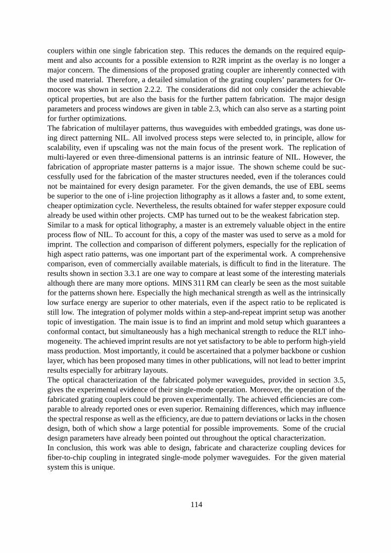
couplers within one single fabrication step. This reduces the demands on the required equip-ment and also accounts for a possible extension toR2R imprint as the overlay is no longer amajor concern. The dimensions of the proposed grating coupler are inherently connected withthe used material. Therefore, a detailed simulation of the grating couplers’ parameters for Or-mocore was shown in section2.2.2. The considerations did not only consider the achievableoptical properties, but are also the basis for the further pattern fabrication. The major designparameters and process windows are given in table2.3, which can also serve as a starting pointfor further optimizations.The fabrication of multilayer patterns, thus waveguides with embedded gratings, was done us-ing direct patterningNIL. All involved process steps were selected to, in principle,allow forscalability, even if upscaling was not the main focus of the present work. The replication ofmulti-layered or even three-dimensional patterns is an intrinsic feature ofNIL. However, thefabrication of appropriate master patterns is a major issue. The shown scheme could be suc-cessfully used for the fabrication of the master structuresneeded, even if the tolerances couldnot be maintained for every design parameter. For the given demands, the use ofEBL seemsbe superior to the one of i-line projection lithography as itallows a faster and, to some extent,cheaper optimization cycle. Nevertheless, the results obtained for wafer stepper exposure couldalready be used within other projects.CMP has turned out to be the weakest fabrication step.Similar to a mask for optical lithography, a master is an extremely valuable object in the entireprocess flow ofNIL. To account for this, a copy of the master was used to serve as amold forimprint. The collection and comparison of different polymers, especially for the replication ofhigh aspect ratio patterns, was one important part of the experimental work. A comprehensivecomparison, even of commercially available materials, is difficult to find in the literature. Theresults shown in section3.3.1are one way to compare at least some of the interesting materialsalthough there are many more options. MINS 311 RM can clearly be seen as the most suitablefor the patterns shown here. Especially the high mechanicalstrength as well as the intrinsicallylow surface energy are superior to other materials, even if the aspect ratio to be replicated isstill low. The integration of polymer molds within a step-and-repeat imprint setup was anothertopic of investigation. The main issue is to find an imprint and mold setup which guarantees aconformal contact, but simultaneously has a high mechanical strength to reduce theRLT inho-mogeneity. The achieved imprint results are not yet satisfactory to be able to perform high-yieldmass production. Most importantly, it could be ascertainedthat a polymer backbone or cushionlayer, which has been proposed many times in other publications, will not lead to better imprintresults especially for arbitrary layouts.The optical characterization of the fabricated polymer waveguides, provided in section3.5,gives the experimental evidence of their single-mode operation. Moreover, the operation of thefabricated grating couplers could be proven experimentally. The achieved efficiencies are com-parable to already reported ones or even superior. Remainingdifferences, which may influencethe spectral response as well as the efficiency, are due to pattern deviations or lacks in the chosendesign, both of which show a large potential for possible improvements. Some of the crucialdesign parameters have already been pointed out throughoutthe optical characterization.In conclusion, this work was able to design, fabricate and characterize coupling devices forfiber-to-chip coupling in integrated single-mode polymer waveguides. For the given materialsystem this is unique.
114

4.2 Outlook
The consideration of design, master fabrication, imprint and characterization revealed manyprocess weaknesses, which will be in future works. In the following, some of the importantremaining issues should be mentioned and, to some extent, approaches to improve or evenavoid them are discussed.
4.2.1 Design
The design of the integrated optical chip can be discussed regarding the optical performance,the fabrication process as well as the principle architecture.
The characterization of the fabricated grating couplers clearly showed the necessity to notonly consider the desired light interaction with the given patterns, but also to take care aboutreflections and stray light. As the efficiency of the couplingelements is still low, light scatteredinto the cladding and substrate may cause non-negligible cross-talk between adjacent transmis-sion lines. Moreover, the back-reflections at waveguide facets (cf. section3.5.3.2) have to beavoided, e.g. using oblique waveguide ends. A thorough investigation and minimization of theback-reflections caused by the gratings should also be included in future works, this may requirethe use of an off-axis coupling scheme [87]. In general, the integration of defined absorbers tohandle stray-light in integrated polymer chips might be useful.The dependence of the output spectrum upon the cladding thickness was shown in equation(2.19). As already discussed, the inhomogeneity of the cladding andRLT have to be minimizeddrastically. The pattern density has a strong influence on the RLT (cf. figure3.27). It shouldtherefore be kept within closer margins, including the defined placement of dummy patterns.
A more general design change would be the use of fully etched gratings for coupling, whichwere already proposed forSOI[19]. The use of only one height level would drastically simplifythe fabrication process. However, an efficient first order grating coupler would require aspectratios of approx.4. With the current technology it is unlikely that these can bereplicated.This also holds true if a first order reflector should be replicated (cf. section3.4.3). As themaster fabrication for such a structure is one of the crucialdesign points, future designs shoulduse higher order reflectors with the distinct goal to reduce the patterns aspect ratio. Possibledesigns were outlined in section2.2.2.1.Instead of optimizing both, waveguide and bottom reflector,the application of a highRI overlayshould be preferred. The use of a silicon overlay was simulated to allow efficiencies up to35 %.This would correnspond to an enhancement factor of roughly18, whereas the respective valuefor both reflectors would be below2.
The necessary alignment accuracy between single-mode fibers and integrated waveguidescould be successfully extended with the fabricated structures. Nevertheless, a positioning toler-ance in the range of severalµm (cf. figure3.32) still requires an additional alignment strategy.Many of the solutions shown previously in other publications focused on the integration ofalignment features for in-plane coupling [177–180]. A different solution for out-of-plane cou-pling could be found in the scheme depicted in figure4.1, which was already proposed in asimilar fashion previously [181–183]. Herein, aTSV serves as a passive alignment feature forthe fiber. The configuration further allows the separation ofthe optical coupling scheme and a
115
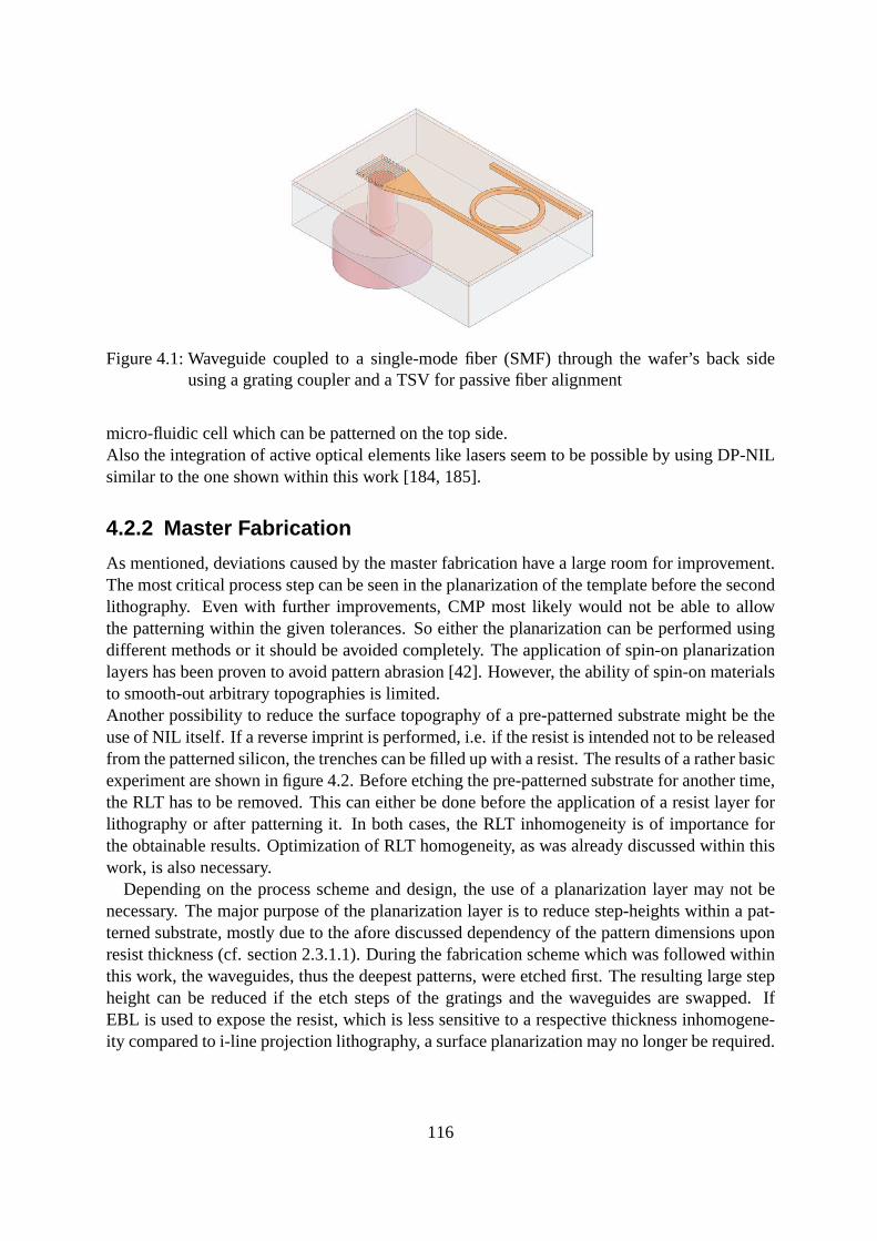
Figure 4.1: Waveguide coupled to asingle-mode fiber (SMF)through the wafer’s back sideusing a grating coupler and aTSV for passive fiber alignment
micro-fluidic cell which can be patterned on the top side.Also the integration of active optical elements like lasersseem to be possible by usingDP-NILsimilar to the one shown within this work [184, 185].
4.2.2 Master Fabrication
As mentioned, deviations caused by the master fabrication have a large room for improvement.The most critical process step can be seen in the planarization of the template before the secondlithography. Even with further improvements,CMP most likely would not be able to allowthe patterning within the given tolerances. So either the planarization can be performed usingdifferent methods or it should be avoided completely. The application of spin-on planarizationlayers has been proven to avoid pattern abrasion [42]. However, the ability of spin-on materialsto smooth-out arbitrary topographies is limited.Another possibility to reduce the surface topography of a pre-patterned substrate might be theuse ofNIL itself. If a reverse imprint is performed, i.e. if the resistis intended not to be releasedfrom the patterned silicon, the trenches can be filled up witha resist. The results of a rather basicexperiment are shown in figure4.2. Before etching the pre-patterned substrate for another time,theRLT has to be removed. This can either be done before the application of a resist layer forlithography or after patterning it. In both cases, theRLT inhomogeneity is of importance forthe obtainable results. Optimization ofRLT homogeneity, as was already discussed within thiswork, is also necessary.
Depending on the process scheme and design, the use of a planarization layer may not benecessary. The major purpose of the planarization layer is to reduce step-heights within a pat-terned substrate, mostly due to the afore discussed dependency of the pattern dimensions uponresist thickness (cf. section2.3.1.1). During the fabrication scheme which was followed withinthis work, the waveguides, thus the deepest patterns, were etched first. The resulting large stepheight can be reduced if the etch steps of the gratings and thewaveguides are swapped. IfEBL is used to expose the resist, which is less sensitive to a respective thickness inhomogene-ity compared to i-line projection lithography, a surface planarization may no longer be required.
116

Figure 4.2: Silicon surface planarization by defined trenchfilling usingNIL (unpatterned mold:MD 40; resist: UVcur21SF)
4.2.3 Imprint
The replication of the desired patterns was difficult and still reveals issues in its current state.For a potential mass production, the edge exclusion area of an imprint site has to be minimized.This was introduced to avoid the edge-effects originating from the pressure drop at the moldedge (cf. section3.4.3). The area which is influenced by the edge correlates to the imprintpressure. The reduction of the applied imprint pressure is therefore desirable. This may requirean improvement of the molds’ planarity.As was outlined, the mold has to achieve conformal contact over its entire area. Flexible poly-mer working stamps can account for this problem even on relatively inhomogeneous surfaces.In contrast, the reduction of theRLT inhomogeneity for arbitrary layouts demands stiff moldmaterials. These two contrary trends require an optimization of the mold stack used for imprint-ing. As the fabrication of different mold stacks, which willmost likely also include differentmaterials, is a sophisticated task, the prediction of theirimprint performance using simulationis highly desirable.Despite other factors, the shrinkage inherent to UV-curable polymers limits the achievable di-mensions usingDP-NIL. A distinct investigation of polymer shrinkage, includingits depen-dence upon pattern size, shape andRLT is a prerequisite for establishing highly reliable pro-cesses. Moreover, the influence of a working mold upon the pattern transfer fidelity needs to beanalyzed quantitatively. The same holds true for the mold lifetime and possible degradations.For step-and-repeat imprinting, the mold lifetime is of increased importance, as several tens oreven hundreds of imprints have to be performed to pattern onesingle wafer.Also, the aspect ratio within the mold as well as the imprint achievable so far should be subjectto enhancements in the future, as there is a clear demand for those patterns in many applications.Here, a detailed analysis and understanding of the surface interactions is inevitable.
117

118

List of Publications
International Journals
1. R. Hensel and A. Finn(equal contribution), R. Helbig, H.-G. Braun, C. Neinhuis, W.-J.Fischer, and C. Werner. Biology-inspired omniphobic surfaces by reverse imprint lithog-raphy (accepted). Advanced Materials.http://dx.doi.org/10.1002/adma.201305408
2. M. Waegner, A. Finn, G. Suchaneck, G. Gerlach, and L. M. Eng. Connected Lead Zir-conate Titanate Nanodot Arrays for Perspective Functional. Journal of Nanoscience.http://dx.doi.org/10.1155/2013/587345
3. A. Finn, B. Lu, R. Kirchner, X. Thrun, K. Richter, and W.-J. Fischer. High aspect ratiopattern collapse of polymeric UV-nano-imprint molds due tocleaning. MicroelectronicEngineering, 110:112-118, October 2013. ISSN 0167-9317.http://dx.doi.org/10.1016/j.mee.2013.02.065
4. L. Teng, M. Plötner, A. Türke, B. Adolphi, A. Finn, R. Kirchner, and W.-J. Fischer.Nanoimprint Assisted Inkjet Printing to Fabricate Sub-micron Channel Organic Field Ef-fect Transistors. Microelectronic Engineering, 110:292-297, October 2013. ISSN 0167-9317.http://dx.doi.org/10.1016/j.mee.2013.02.027
5. R. Kirchner, A. Finn, R. Landgraf, L. Nüske, M. Vogler, and W.-J. Fischer. UV-basedNanoimprint Lithography: Towards Direct Patterning of Functional Polymers. J. Pho-topolym. Sci. Technol. 25/2, 197-206, 2012.
6. A. Finn, R. Hensel, F. Hagemann, R. Kirchner, A. Jahn, and W.-J. Fischer. GeometricalProperties of Multilayer Nano-Imprint-Lithography Moldsfor Optical Applications. Mi-croelectronic Engineering 98, 284-287, October 2012.http://dx.doi.org/10.1016/j.mee.2012.04.022
7. R. Kirchner, L. Nüske, A. Finn, B. Lu, and W.-J. Fischer. Stamp-and-repeat UV-imprint-ing of spin-coated films: Pre-exposure and imprint defects.Microelectronic Engineering97, 117-121, September 2012.http://dx.doi.org/10.1016/j.mee.2012.03.037
8. A. Finn, M. Schossig, V. Norkus, and G. Gerlach. Microstructured Surfaces on LiTaO3-Based Pyroelectric Infrared Detectors. IEEE Sensors Journal 11, 2204-2211, October2011.http://dx.doi.org/10.1109/JSEN.2011.2128307
119

9. R. Kirchner, A. Finn, L. Teng, M. Plötner, A. Jahn, L. Nüske, and W.-J. Fischer. UV-nanoimprinting using non-transparent molds and non-transparent substrates. Microelec-tronic Engineering 88, 2004-2008, August 2011.http://dx.doi.org/10.1016/j.mee.2011.01.066
Book Chapters
10. T. Schuster, R. Landgraf, A. Finn, and M. Mertig. Biosensing with Optical Waveguides.in G. Gerlach and K.-J. Wolter, Bio and Nano Packaging Techniques for Electron Devices:Advances in Electronic Device Packaging. (Springer: 2012).
International Conferences
11. A. Finn, R. Landgraf, J.-P. Mehner, and W.-J. Fischer. Stamp-and-Repeat Imprint us-ing Polymer Molds with Rigid or Flexible Backbone. 12th Int. Conf. on Nanoimprintand Nanoprint Technology (NNT 2013), Barcelona, Spain, 2013(poster)[Best PosterAward] .
12. L. Teng, A. Finn, M. Plötner, F. Hagemann, and W.-J. Fischer. Sub-100 nm ChannelP3HT-OFET Fabricated by Wafer-Scale Nanoimprint and its ACTest. 12th Int. Conf. onNanoimprint and Nanoprint Technology (NNT 2013), Barcelona, Spain, 2013 (oral).
13. A. Finn, R. Hensel, S. Killge, C. Werner, and W.-J. Fischer. Fabrication of SpringtailInspired Surface Features with Undercuts by Direct Replication. 39th Int. Conf. onMicro and Nano Engineering 2013 (MNE 2013), London, United Kingdom, 2013 (oral).
14. L. Teng, A. Finn, M. Plötner, F. Hagemann, and W.-J. Fischer. Sub-100 nm ChannelOrganic Field Effect Transistor fabricated by Wafer-ScaleNanoimprint Lithography withPolymer Templates. 39th Int. Conf. on Micro and Nano Engineering 2013 (MNE 2013),London, United Kingdom, 2013 (oral).
15. R. Hensel, A. Finn, R. Helbig, H.-G. Braun, C. Neinhuis, W.-J. Fischer and C. Werner.Springtail skin inspired omniphobic polymer membranes. Engineering Life 2013: Bio-molecular principles for novel methods and materials, September 17-18, Dresden, Ger-many, 2013 (poster)[2nd Poster Price].
16. A. Finn, R. Hensel, A. Jahn, S. Killge, C. Werner, and W.-J. Fischer. Fabrication of Poly-mer Structures with Undercuts by Reverse Imprint Lithography. 57th Int. Conf. on Elec-tron, Ion, and Photon Beam Technology and Nanofabrication (EIPBN 2013), Nashville,United States, 2013 (poster)[invited] .
17. A. Finn, R. Kirchner, R. Landgraf, A. Hiess, X. Thrun, L. Nüske, and W.-J. Fischer.Stamp-and-Repeat UV Direct Patterning using Polymer Molds.10th Int. Workshop onHigh Aspect Ratio Micro and Nano System Technology (HARMNST 2013), Berlin, Ger-many, 2013 (oral).
120

18. R. Hensel, A. Finn, R. Helbig, C. Neinhuis, W.-J. Fischer and C. Werner. Porous andflex-ible polymer membranes to mimic the omniphobic characteristics of springtail skin. 3rdInt. Conf. on Multifunctional, Hybrid and Nanomaterials, Sorrento, Italy, 2013 (poster).
19. R. Hensel, A. Finn, R. Helbig, H.-G. Braun, C. Neinhuis, W. Fischer and C. Werner.Polymer membranes with omniphobic wetting characteristics inspired by springtail skinmorphology. European Symposium on Biomaterials and Related Areas (BioMAT 2013),Weimar, Germany, 2013 (poster).
20. R. Kirchner, A. Finn, A. Chares, M. Vogler, and W.-J. Fischer. Influence of SolventRemoval and UV-exposure on Feature Shrinkage in UV-NIL Direct Pattering. 11th Int.Conf. on Nanoimprint and Nanoprint Technology (NNT 2012), 2012 (poster).
21. R. Kirchner, R. Landgraf, A. Finn, M. Vogler, W.-J. Fischer. Simple UV direct imprint-ing of photonic microring resonators with high quality fromspin coated hybrid-polymerfilms. 11th Int. Conf. on Nanoimprint and Nanoprint Technology (NNT 2012), 2012(poster).
22. A. Finn, R. Hensel, A. Jahn, S. Killge, C. Werner, and W.-J. Fischer. Polymer Structureswith Undercuts by Reverse Imprint Lithography. 38th Int. Conf. on Micro and NanoEngineering 2012 (MNE 2012), 2012. (poster)[Best Poster Award]
23. L. Teng, M. Plötner, A. Türke, B. Adolphi, A. Finn, R. Kirchner, and W.-J. Fischer.Nanoimprint Assisted Inkjet Print to Fabricate Sub-micronChannel Organic Field Ef-fect Transistors. in Proc. 38th Int. Conf. on Micro and Nano Engineering 2012 (MNE2012), 2012 (oral).
24. M. Waegner, G. Suchaneck, G. Gerlach, L. M. Eng and A. Finn. Nano-patterned PZTfilms for perspective fucntional materials. Applications of Ferroelectrics held jointlywith 2012 European Conference on the Applications of Polar Dielectrics and 2012 In-ternational Symp Piezoresponse Force Microscopy and Nanoscale Phenomena in PolarMaterials (ISAF/ECAPD/PFM), 2012 Intl Symp 1-3 (2012).
25. A. Finn, B. Lu, R. Kirchner, K. Richter, and W.-J. Fischer. Cleaning Defects of Soft UVNanoimprint Molds for High Aspect-Ratio Features. 56th Int.Conf. on Electron, Ion andPhoton Beams (EIPBN 2012), 2012 (poster).
26. R. Kirchner, A. Finn, R. Landgraf, L. Nüske, M. Vogler, and W.-J. Fischer. UV-basedNanoimprint Lithography: Toward Direct Patterning of Functional Polymers. 3rd Int.Conf. on Physics Science and Technology ICPST 2012, (oral)[invited] .
27. R. Kirchner, L. Teng, A. Finn, and W.-J. Fischer. UV-assisted Nanoimprinting usingOpaque Molds and Substrates. in Proc. 1st Annual World Congress of Nano-Science &Technology (NANO S&T 2011), (Dalian), October 2011 (oral)[invited]
28. A. Finn, F. Hagemann, R. Hensel, R. Kirchner, A. Jahn, and W.-J. Fischer. Characteri-sation of the Geometrical Properties of Multilayer Nano-Imprint-Lithography Molds for
121

Optical Applications. in Proc. 37th Int. Conf. on Micro and Nano Engineering 2011(MNE 2011), 2011 (oral).
29. R. Kirchner, L. Nüske, A. Finn, B. Lu, and W.-J. Fischer. Stamp-and-Repeat UV Imprint-ing of Spin-Coated Films: Pre-Exposure and Imprint Defects.in Proc. 37th Int. Conf. onMicro and Nano Engineering 2011 (MNE 2011), 2011 (oral).
30. R. Landgraf, T. Haugwitz, R. Kirchner, A. Finn, and W.-J. Fischer. Planar Optical Wave-guide Design for UV-Nanoimprinted Microring Resonator BasedBiosensors. in Proc.IEEE Sensors 2011, 2011
31. R. Kirchner, A. Finn, L. Teng, M. Plötner, A. Jahn, L. Nüske, and W.-J. Fischer. UV-Nanoimprinting Using Non-Transparent Molds and Non-Transparent Substrates. in Proc.36th Int. Conf. on Micro and Nano Engineering 2010 (MNE 2010),2010 (poster).
National Conferences
32. R. Landgraf, R. Kirchner, A. Finn, S. Arndt, T. Haugwitz, F. Deicke, and W.-J. Fischer.Polymer Microring Resonator Directly Patterned by Multilevel-Nanoimprint: Integra-tion into a Biosensor System with a Miniaturized MicrofluidicSystem. Sensoren undMesssysteme 2012
33. R. Landgraf, R. Kirchner, T. Haugwitz, A. Finn, F. Deicke, and W.-J. Fischer. Polymerop-tische Mikroringresonatoren für biosensorische Anwendungen: Design und Integration.Microsys 2012
34. R. Landgraf, A. Finn, R. Kirchner, T. Haugwitz, S. Arndt, F. Deicke, and W.-J. Fischer.Biosensor System with Polymer Microring Resonators Manufactured by Multilevel-UV-Nanoimprint. in Proc. Mikro-System-Technik Kongress 2011, 2011
35. A. Finn, A. Jahn, R. Kirchner, U. Künzelmann, J. He, M. Waegner, and Wolf-JoachimFischer. Multilayer Nano-Imprint-Lithography Mold Fabrication Process. in 3rd GMMWorkshop Mikro-Nano-Integration, GMM Fachbericht 68, pp.8-12, VDE Verlag GmbH,3th-4th March 2011. ISBN 978-3-8007-3334-7 [in English]
122

Bibliography
[1] K. Iga. Encyclopedic handbook of integrated optics. CRC, Boca Raton, 2006.1
[2] C. Ciminelli, C. M. Campanella, F. Dell’Olio, C. E. Campanella,and M. N. Armenise.Label-free optical resonant sensors for biochemical applications. Progress in QuantumElectronics, 37(2):51–107, March 2013.1, 2.1.2
[3] D. Rezzonico, A. Guarino, C. Herzog, M. Jazbinsek, and P. Gunter. High-finesse later-ally coupled organic-inorganic hybrid polymer microring resonators for VLSI photonics.IEEE Photonics Technology Letters, 18(7):865–867, 2006.1, 2.1
[4] A. Madani, H. Azarinia, and H. Latifi. Design and fabrication of a polymer micro ringresonator with novel optical material at add/drop geometryusing laser beam direct writelithography technique.Optik - International Journal for Light and Electron Optics,124(14):1746–1748, July 2013.1
[5] C.-Y. Chao and L. J. Guo. Biochemical sensors based on polymer microrings with sharpasymmetrical resonance.Applied Physics Letters, 83(8):1527–1529, 2003.1, 1.2
[6] M. Mancuso, J. M. Goddard, and D. Erickson. Nanoporous polymer ring resonators forbiosensing.Optics Express, 20(1):245–255, January 2012.1
[7] L. Wang, J. Ren, X. Han, T. Claes, X. Jian, P. Bienstman, R. Baets, M. Zhao, and G. Mor-thier. A label-free optical biosensor built on a low-cost polymer platform.IEEE Photon-ics Journal, 4(3):920–930, 2012.1, 2.1.2, 2.2, 2.3.3
[8] R. Landgraf.Photonic Biosensing Using Polymer Microring Resonators (working title).PhD thesis, 2013.1, 2, 2.1.2, 3.5, 3.5.1
[9] R. Kirchner. On UV-nanoimprint-lithography as direct patterning tool for polymericmicrosystems. TUDpress Verlag der Wiss., 2012.1, 1.3, 2, 2.1.1, 2.4.2, 2.4.3.1, 3, 3.3.2,3.4.3
[10] G. Ghosh.Handbook of optical constants of solids: five-volume set. Academic Press,San Diego, 1998.1.1
[11] A. Sure, T. Dillon, J. Murakowski, C. Lin, D. Pustai, and D. Prather. Fabrication andcharacterization of three-dimensional silicon tapers.Optics Express, 11(26):3555–3561,December 2003.1.1, 3.5.3.2
[12] B. Kessler, M. Frish, C. Manolatou, M. Fritze, J. Knecht, C.Bozler, C. Keast, J. Fijol,S. Jacobson, P. Keating, J. LeBlanc, and E. Fike. 3D mode converters for SOI integratedoptics. pages 165–166, 2002.1.1
123

[13] G. Roelkens, D. Van Thourhout, R. Baets, R. Nötzel, and M. Smit. Laser emissionand photodetection in an InP/InGaAsP layer integrated on and coupled to a silicon-on-insulator waveguide circuit.Optics Express, 14(18):8154–8159, 2006.1.1
[14] V. R. Almeida, R. R. Panepucci, and M. Lipson. Nanotaper forcompact mode conver-sion. Optics Letters, 28(15):1302–1304, 2003.
[15] T. Shoji, T. Tsuchizawa, T. Watanabe, K. Yamada, and H. Morita. Low loss mode sizeconverter from 0.3µm square si wire waveguides to singlemode fibres.Electronics Let-ters, 38(25):1669–1670, 2002.1.1
[16] D. Taillaert, W. Bogaerts, P. Bienstman, T. Krauss, P. vanDaele, I. Moerman, S. Ver-stuyft, K. De Mesel, and R. Baets. An out-of-plane grating coupler for efficient butt-coupling between compact planar waveguides and single-mode fibers. IEEE Journal ofQuantum Electronics, 38(7):949–955, 2002.1.1, 2.2.2, 2.2.2.1, 2.2.2.2, 2.2.2.4, 3.5.3.1
[17] T. W. Ang, G. Reed, A. Vonsovici, A. G. R. Evans, P. R. Routley,and M. R. Josey.Effects of grating heights on highly efficient unibond SOI waveguide grating couplers.IEEE Photonics Technology Letters, 12(1):59–61, 2000.2.2.2
[18] G. Maire, L. Vivien, G. Sattler, A. Kazmierczak, B. Sanchez, K. B. Gylfason, A. Griol,D. Marris-Morini, E. Cassan, D. Giannone, H. Sohlström, and D. Hill. High efficiencysilicon nitride surface grating couplers.Optics Express, 16(1):328, 2008.1.1
[19] B. Schmid, A. Petrov, and M. Eich. Optimized grating coupler with fully etched slots.Optics Express, 17(13):11066–11076, June 2009.1.1, 4.2.1
[20] M. Antelius, K. B. Gylfason, and H. Sohlström. An apodized SOI waveguide-to-fiber surface grating coupler for single lithography silicon photonics. Opt. Express,19(4):3592–3598, 2011.1.1
[21] X. Chen, C. Li, C. Fung, S. Lo, and H. Tsang. Apodized waveguide grating couplers forefficient coupling to optical fibers.IEEE Photonics Technology Letters, 22(15):1156–1158, 2010.1.1, 2.2.2
[22] X. Chen, C. Li, and H. K. Tsang. Fabrication-tolerant waveguide chirped grating couplerfor coupling to a perfectly vertical optical fiber.Photonics Technology Letters, IEEE,20(23):1914 –1916, December 2008.1.1
[23] W. Driemeier. Bragg-effect grating couplers integrated in multicomponent polymericwaveguides.Optics Letters, 15(13):725–727, July 1990.1.1
[24] J. Paterson, A. Natansohn, P. Rochon, C. L. Callender, and L. Robitaille. Opticallyinscribed surface relief diffraction gratings on azobenzene-containing polymers for cou-pling light into slab waveguides.Applied Physics Letters, 69(22):3318, 1996.1.1
[25] R. Waldhäusl, B. Schnabel, P. Dannberg, E.-B. Kley, A. Bräuer, and W. Karthe. Effi-cient coupling into polymer waveguides by gratings.Applied Optics, 36(36):9383–9390,December 1997.1.1, 2.2.2.2
124

[26] R. Bruck, P. Muellner, N. Kataeva, A. Koeck, S. Trassl, V. Rinnerbauer, K. Schmidegg,and R. Hainberger. Flexible thin-film polymer waveguides fabricated in an industrialroll-to-roll process.Applied Optics, 52(19):4510–4514, July 2013.1.1, 3.5.2
[27] R. Bruck and R. Hainberger. Efficient coupling of narrow beams into polyimidewaveguides by means of grating couplers with high-index coating. Applied Optics,49(10):1972–1978, April 2010.1.1, 2.2.2, 2.2.2.3, 3.5.3.1, 3.5.3.2, 3.5.3.2
[28] M. Wang, J. Hiltunen, S. Uusitalo, J. Puustinen, J. Lappalainen, P. Karioja, and R. Myl-lylä. Fabrication of optical inverted-rib waveguides using UV-imprinting. Microelec-tronic Engineering, 88(2):175–178, February 2011.1.1
[29] M. E. Pollard, S. J. Pearce, R. Chen, S. Oo, and M. D. B. Charlton. Polymer wave-guide grating couplers for low-cost nanoimprinted integrated optics. volume 8264, pages826418–826418–8, 2012.1.1
[30] C. Y. Chao.Polymer microring resonator and its application as a biosensor. PhD thesis,University of Michigan, 2005.1.1, 2.1, 2.1.1, 2.1.2, 2.2, 2.3.1.2, 2.3.3
[31] J. Hiltunen, M. Wang, M. Hiltunen, J. Puustinen, J. Lappalainen, S. Pearce, M. Charlton,and P. Karioja. UV-imprinting of single-mode polymeric waveguides. volume 8069,pages 80690U–80690U–6, 2011.1.1
[32] D. M. Tennant. Progress and issues in e-beam and other top down nanolithography.Journal of Vacuum Science & Technology A: Vacuum, Surfaces,and Films, 31(5):050813,2013.1.2
[33] C. R. K. Marrian and D. M. Tennant. Nanofabrication.Journal of Vacuum Science &Technology A: Vacuum, Surfaces, and Films, 21(5):S207–S215, 2003.1.2
[34] H. Schift. Nanoimprint lithography: An old story in modern times? a review.Jour-nal of Vacuum Science & Technology B: Microelectronics and Nanometer Structures,26(2):458–480, 2008.1.2, 3.4.2
[35] S. Y. Chou, P. R. Krauss, and P. J. Renstrom. Imprint of sub-25 nm vias and trenches inpolymers.Applied Physics Letters, 67(21):3114–3116, 1995.1.2
[36] F. Hua, Y. Sun, A. Gaur, M. A. Meitl, L. Bilhaut, L. Rotkina,J. Wang, P. Geil, M. Shim,J. A. Rogers, and A. Shim. Polymer imprint lithography with molecular-scale resolution.Nano Letters, 4(12):2467–2471, December 2004.1.2
[37] S. MacDonald, G. Hughes, M. Stewart, F. Palmieri, and C. G. Willson. Design andfabrication of highly complex topographic nano-imprint template for dual damascenefull 3-d imprinting. volume 5992, pages 59922F–59922F–9, 2005. 1.2
[38] V. Reboud, I. Obieta, L. Bilbao, V. Saez-Martinez, M. Brun,F. Laulagnet, and S. Landis.Imprinted hydrogels for tunable hemispherical microlenses. Microelectronic Engineer-ing, 111:189–192, November 2013.
125

[39] A. Finn, A. Jahn, R. Kirchner, U. K\ünzelmann, J. He, M. Waegner, and W. J. Fis-cher. Multilayer nano-imprint-lithography mold fabrication process. InMikro-Nano-Integration, volume 68 ofGMM-FB, pages 8–12. VDE Verlag, 2011.1.2
[40] S. Mollenbeck, N. Bogdanski, M. Wissen, H. C. Scheer, J. Zajadacz, and K. Zimmer.Multiple replication of three dimensional structures withundercuts. Journal of Vac-uum Science Technology B: Microelectronics and Nanometer Structures, 25(1):247–251,2007.1.2
[41] A. Finn, R. Hensel, A. Jahn, S. Killge, C. Werner, and W.-J.Fischer. Fabrication ofpolymer structures with undercuts by reverse imprint lithography (invited). Nashville,Tennessee, 2013.1.2
[42] S. Landis, V. Reboud, T. Enot, and C. Vizioz. Three dimensional on 300 mm waferscale nano imprint lithography processes.Microelectronic Engineering, 110:198–203,October 2013.1.2, 2.3.2, 3.2.2, 3.4.3, 4.2.2
[43] A. Schleunitz, C. Spreu, M. Vogler, H. Atasoy, and H. Schift. Combining nanoim-print lithography and a molecular weight selective thermalreflow for the generation ofmixed 3D structures.Journal of Vacuum Science & Technology B: MicroelectronicsandNanometer Structures, 29(6):06FC01, 2011.1.2, 2.3.1
[44] I. Fernandez-Cuesta, A. L. Palmarelli, X. Liang, J. Zhang, S. Dhuey, D. Olynick, andS. Cabrini. Fabrication of fluidic devices with 30 nm nanochannels by direct imprinting.Journal of Vacuum Science & Technology B: Microelectronicsand Nanometer Structures,29(6):06F801, 2011.1.2
[45] Y. Xia and G. M. Whitesides. Soft lithography.Annual Review of Materials Science,28(1):153–184, 1998.1.2, 2.4.3.1
[46] A. Kumar and G. M. Whitesides. Features of gold having micrometer to centime-ter dimensions can be formed through a combination of stamping with an elastomericstamp and an alkanethiol ‘‘ink’’ followed by chemical etching. Applied Physics Letters,63(14):2002, October 1993.1.2
[47] Y. Xia, E. Kim, X.-M. Zhao, J. A. Rogers, M. Prentiss, and G. M. Whitesides. Com-plex optical surfaces formed by replica molding against elastomeric masters.Science,273(5273):347–349, 1996.1.2
[48] T. Senn, J. P. Esquivel, M. Lörgen, N. Sabaté, and B. Löchel. Replica molding formultilevel micro-/nanostructure replication.Journal of Micromechanics and Microengi-neering, 20(11):115012, November 2010.1.2
[49] S. H. Ahn and L. J. Guo. Large-area roll-to-roll and roll-to-plate nanoimprint lithography:A step toward high-throughput application of continuous nanoimprinting. ACS Nano,3(8):2304–2310, 2009.1.2
126

[50] W. Zhang, F. Ding, W.-D. Li, Y. Wang, J. Hu, and S. Y. Chou. Giant and uniformfluorescence enhancement over large areas using plasmonic nanodots in 3D resonantcavity nanoantenna by nanoimprinting.Nanotechnology, 23(22):225301, June 2012.1.2
[51] K. Kumar, H. Duan, R. S. Hegde, S. C. W. Koh, J. N. Wei, and J. K. W. Yang. Printingcolour at the optical diffraction limit.Nature Nanotechnology, 7(9):557–561, September2012.1.2
[52] T. Senn, O. Kutz, C. Weniger, J. Li, M. Schoengen, H. Lochel, J. Wolf, P. Gottert, andB. Lochel. Integration of moth-eye structures into a poly(dimethylsiloxane) stamp forthe replication of functionalized microlenses using UV-nanoimprint lithography.Jour-nal of Vacuum Science & Technology B: Microelectronics and Nanometer Structures,29(6):061601, 2011.1.2
[53] V. Reboud, N. Kehagias, T. Kehoe, G. Leveque, C. Mavidis, M. Kafesaki, and C. So-tomayor Torres. Nanoimprinted plasmonic crystals for light extraction applications.Mi-croelectronic Engineering, 87(5-8):1367–1369, 2011.1.2
[54] C. Peroz, S. Dhuey, A. Goltsov, M. Volger, B. Harteneck, I.Ivonin, A. Bugrov, S. Cabrini,S. Babin, and V. Yankov. Digital spectrometer-on-chip fabricated by step and re-peat nanoimprint lithography on pre-spin coated films.Microelectronic Engineering,88(8):2092–2095, August 2011.1.2
[55] C. Peroz, J.-C. Galas, L. Le Gratiet, Y. Chen, and J. Shi. Compact dye laser on a chip fab-ricated by ultraviolet nanoimprint lithography.Applied Physics Letters, 89(24):243109–243109–3, December 2006.1.2
[56] C. Vannahme, S. Klinkhammer, M. B. Christiansen, A. Kolew,A. Kristensen, U. Lem-mer, and T. Mappes. All-polymer organic semiconductor laser chips: Parallel fabricationand encapsulation.Optics Express, 18(24):24881–24887, 2010.1.2
[57] R. Kirchner, M. Kaiser, B. Adolphi, R. Landgraf, and W. Fischer. Chemical functionalpolymers for direct UV assisted nanoimprinting of polymeric photonic microring res-onators.physica status solidi (a), 208(6):1308–1314, June 2011.1.2
[58] R. Kirchner, L. Nüske, A. Finn, B. Lu, and W.-J. Fischer. Stamp-and-repeat UV-imprinting of spin-coated films: Pre-exposure and imprint defects.Microelectronic En-gineering, 97:117–121, September 2012.2.4.1, 2.4.3.1, 2.4.4, 3.4.3
[59] R. Kirchner, A. Finn, R. Landgraf, L. Nueske, L. Teng, M. Vogler, and W.-J. Fischer.Direct UV-Imprint of hybrid-polymer photonic microring resonators and their character-ization. tbp. 1.2, 2.1.1, 2.1, 2.2, 2.4.1, 2.4.1, 2.4.3.1
[60] W. Bogaerts, P. De Heyn, T. Van Vaerenbergh, K. De Vos, S. Kumar Selvaraja, T. Claes,P. Dumon, P. Bienstman, D. Van Thourhout, and R. Baets. Silicon microring resonators.Laser & Photonics Reviews, 2012.2.1, 2.1.2
127

[61] B. E. A. Saleh and M. C. Teich.Fundamentals of Photonics. Wiley, Hoboken, 2 edition,2007.2.1, 2.4
[62] MicroResist Technology GmbH. Ormocore data sheet, November 2012.2.1.1
[63] U. Streppel, P. Dannberg, C. Wächter, A. Bräuer, and R. Kowarschik. Formation ofmicro-optical structures by self-writing processes in photosensitive polymers.AppliedOptics, 42(18):3570–3579, June 2003.2.1.1
[64] A. Fallahkhair, K. S. Li, and T. E. Murphy. Vector finite difference modesolver foranisotropic dielectric waveguides.Journal of Lightwave Technology, 26(11):1423–1431,June 2008.2.1.1
[65] S. G. Johnson and J. D. Joannopoulos. Block-iterative frequency-domain methods formaxwell’s equations in a planewave basis.Opt. Express, 8(3):173–190, 2001.2.1.1
[66] D. A. G. Bruggeman. Dielectric constant and conductivity of mixtures of isotropic ma-terials.Ann Phys-Leipzig, 24:636–679, 1935.2.1.1
[67] Corning. SMF-28e+ data sheet, October 2013.2.1.1
[68] R. Landgraf, T. Haugwitz, R. Kirchner, A. Finn, and W. Fischer. Planar optical wave-guide design for UV-nanoimprinted microring resonator based biosensors. In2011 IEEESensors, pages 596–599, 2011.2.1.1
[69] R. Landgraf, A. Finn, R. Kirchner, T. Haugwitz, F. Deicke,W.-J. Fischer, and S. Arndt.Polymer microring resonator directly patterned by multilevel-nanoimprint: Integrationinto biosensor system with a miniaturized microfluidic system. Tagungsband, page259–267, 2012.2.1.1
[70] C. Vannahme, F. Maier-Flaig, U. Lemmer, and A. Kristensen. Single-mode biologicaldistributed feedback laser.Lab on a Chip, 2013.2.1.1
[71] F. N. Dultsev and A. P. Solowjev. Synthesis and ellipsometric characterization of in-sulating low permittivity SiO2 layers by remote-PECVD usingradio-frequency glowdischarge.Thin Solid Films, 419(1-2):27–32, November 2002.2.1.1
[72] J. He, K. Richter, J. W. Bartha, and S. Howitz. Fabricationof silicon template withsmooth tapered sidewall for nanoimprint lithography.Journal of Vacuum Science &Technology B: Microelectronics and Nanometer Structures, 29(6):06FC16, 2011.2.1.1,2.3.3, 3.2.1, 3.2.4
[73] M. Vogler, S. Wiedenberg, M. Mühlberger, I. Bergmair, T.Glinsner, H. Schmidt, E.-B. Kley, and G. Grützner. Development of a novel, low-viscosity UV-curable polymersystem for UV-nanoimprint lithography.Microelectronic Engineering, 84(5–8):984–988,May 2007.2.1.1
[74] Y. Kawaguchi, F. Nonaka, and Y. Sanada. Fluorinated materials for UV nanoimprintlithography.Microelectronic Engineering, 84(5–8):973–976, May 2007.2.1.1
128

[75] M. Colburn, I. Suez, B. J. Choi, M. Meissl, T. Bailey, S. V. Sreenivasan, J. G. Ekerdt, andC. G. Willsona. Characterization and modeling of volumetric and mechanical propertiesfor step and flash imprint lithography photopolymers.Journal of Vacuum Science &Technology B: Microelectron- ics and Nanometer Structures, 19(6), 2001.2.1.1, 2.4.1,2.4.3.1
[76] L. Wang, Y. Li, M. Garcia Porcel, D. Vermeulen, X. Han, J.Wang, X. Jian, R. Baets,M. Zhao, and G. Morthier. A polymer-based surface grating coupler with an embeddedSi3N4 layer. Journal of Applied Physics, 111(11):114507–114507, 2012.2.2, 2.2.2.3,3.5.3.2, 3.5.3.2
[77] R. Bruck. High index difference polymer waveguide Mach-Zehnder interferometerbiosensor, compatible with injection molding and spin-coating. PhD thesis, UniversitätWien, Wien, 2010.2.2
[78] S. Scheerlinck, D. Taillaert, D. Van Thourhout, and R. Baets. Flexible metal grat-ing based optical fiber probe for photonic integrated circuits. Applied Physics Letters,92(3):031104–031104, 2008.2.2
[79] T. Fricke-Begemann and J. Ihlemann. Direct light-coupling to thin-film waveguides usinga grating-structured GRIN lens.Optics Express, 18(19):19860–19866, September 2010.2.2
[80] A. F. Oskooi, D. Roundy, M. Ibanescu, P. Bermel, J. D. Joannopoulos, and S. G. Johnson.MEEP: a flexible free-software package for electromagneticsimulations by the FDTDmethod.Computer Physics Communications, 181(3):687–702, 2010.2.2
[81] Lumerical Inc. FDTD solutions, 2012.2.2
[82] R. Baets and P. E. Lagasse. Calculation of radiation loss inintegrated-optic tapers andy-junctions.Applied Optics, 21(11):1972–1978, June 1982.2.2.1
[83] B. Luyssaert, P. Bienstman, P. Vandersteegen, P. Dumon, and R. Baets. Efficient nona-diabatic planar waveguide tapers.Journal of Lightwave Technology, 23(8):2462–2468,2005.2.2.1
[84] F. Van Laere, T. Claes, J. Schrauwen, S. Scheerlinck, W. Bogaerts, D. Taillaert,L. O’Faolain, D. Van Thourhout, and R. Baets. Compact focusing grating cou-plers for silicon-on-insulator integrated circuits.Photonics Technology Letters, IEEE,19(23):1919–1921, 2007.2.2.1
[85] E. Hecht.Optik. Oldenbourg, München, 4 edition, 2005.2.2.2
[86] P. Bienstman.Rigorous and efficient modelling of wavelength scale photonic compo-nents. PhD thesis, Universiteit Gent, May 2001.2.2.2
[87] F. Van Laere, G. Roelkens, M. Ayre, J. Schrauwen, D. Taillaert, D. Van Thourhout,T. Krauss, and R. Baets. Compact and highly efficient grating couplers between optical
129

fiber and nanophotonic waveguides.Journal of Lightwave Technology, 25(1):151–156,2007.2.2.2, 2.2.2.2, 3.5.3.2, 4.2.1
[88] D. Taillaert, H. Chong, P. Borel, L. Frandsen, R. De La Rue, and R. Baets. A compacttwo-dimensional grating coupler used as a polarization splitter. IEEE Photonics Tech-nology Letters, 15(9):1249–1251, 2003.2.2.2, 2.2.2.2
[89] F. VanLaere, W. Bogaerts, P. Dumon, G. Roelkens, D. VanThourhout, and R. Baets.Focusing polarization diversity grating couplers in silicon-on-insulator.Journal of Light-wave Technology, 27(5):612–618, March 2009.2.2.2
[90] E. Garmire and T. Tamir.Integrated optics. Springer, Berlin ; Heidelberg, 1979.2.2.2,3.5.3.1
[91] Y. Tang, Z. Wang, L. Wosinski, U. Westergren, and S. He. Highly efficient nonuni-form grating coupler for silicon-on-insulator nanophotonic circuits. Optics Letters,35(8):1290–1292, April 2010.2.2.2
[92] T. Tamir and S. Peng. Analysis and design of grating couplers. Applied Physics A:Materials Science & Processing, 14(3):235–254, November 1977.2.2.2, 2.2.2.3, 3.5.3.1
[93] H. Yamada, M. Nozawa, M. Kinoshita, and K. Ohashi. Vertical-coupling optical interfacefor on-chip optical interconnection.Optics Express, 19(2):698–703, January 2011.2.2.2
[94] M. Born and E. Wolf. Principles of Optics. Pergamon Press, Oxford, 6 edition, 1993.2.2.2.1
[95] N. Eriksson, M. Hagberg, and A. Larsson. Highly directional grating outcouplers withtailorable radiation characteristics.IEEE Journal of Quantum Electronics, 32(6):1038–1047, 1996.2.2.2.2
[96] R. Bruck and R. Hainberger. Efficient small grating couplers for low-index differencewaveguide systems. InProc. SPIE, volume 7218, page 72180A, 2009.2.2.2.3
[97] G. Roelkens, D. Van Thourhout, and R. Baets. High efficiencysilicon-on-insulatorgrating coupler based on a poly-silicon overlay.Optics Express, 14(24):11622–11630,November 2006.2.2.2.3
[98] G. Gerlach and W. Doetzel.Introduction to microsystem technology: a guide for students.Wiley, Chichester, 2008.2.4
[99] C. Mack.Fundamental principles of optical lithography: the science of microfabrication.Wiley, 2008.2.4, 2.3.1.1, 2.3.1.1, 3.2.2
[100] M. G. Stepanova and S. Dew.Nanofabrication: Techniques and Principles. Springer,2012.2.4, 2.3.1, 2.3.1.2
[101] R. Deri and E. Kapon. Low-loss III-V semiconductor optical waveguides.QuantumElectronics, IEEE Journal of, 27(3):626–640, 1991.2.3.1.2
130

[102] M. Aktary, M. Stepanova, and S. K. Dew. Simulation of the spatial distribution andmolecular weight of polymethylmethacrylate fragments in electron beam lithographyexposures.Journal of Vacuum Science & Technology B, 24(2):768–779, March 2006.2.3.1.2
[103] S. A. Rishton and D. P. Kern. Point exposure distribution measurements for proximitycorrection in electron beam lithography on a sub-100 nm scale. Journal of VacuumScience & Technology B, 5(1):135–141, January 1987.2.3.1.2
[104] J. Luo and D. Dornfeld. Material removal mechanism in chemical mechanical polishing:theory and modeling.IEEE Transactions on Semiconductor Manufacturing, 14(2):112–133, 2001.2.3.2, 3.2.3
[105] Y. Nishi. Handbook of semiconductor manufacturing technology. Dekker, New York,2000.2.3.2, 3.2.3
[106] Q. Luo and S. V. Babu. Dishing effects during chemical mechanical polishing of copperin acidic media.Journal of The Electrochemical Society, 147(12):4639–4644, January2000.2.3.2
[107] W.-J. Fischer.Mikrosystemtechnik. Vogel, Würzburg, 2000.2.3.3
[108] M. J. Madou.Fundamentals of microfabrication / the science of miniaturization. CRCPress, Boca Raton, Fla. [u.a.], 2002.2.3.3
[109] B. Wu, A. Kumar, and S. Pamarthy. High aspect ratio silicon etch: A review.Journal ofApplied Physics, 108(5):051101, September 2010.2.3.3, 3.2.4
[110] C. Peroz, S. Dhuey, M. Volger, Y. Wu, D. Olynick, and S. Cabrini. Step and repeat UVnanoimprint lithography on pre-spin coated resist film: a promising route for fabricatingnanodevices.Nanotechnology, 21(44):445301, November 2010.2.3.3, 3.3.1
[111] J. Haisma, M. Verheijen, K. v. d. Heuvel, and J. v. d. Berg. Mold-assisted nanolithogra-phy: A process for reliable pattern replication.Journal of Vacuum Science & TechnologyB, 14(6):4124–4128, November 1996.2.4
[112] B. Heidari, I. Maximov, E.-L. Sarwe, and L. Montelius. Large scale nanolithographyusing nanoimprint lithography.Journal of Vacuum Science & Technology B, 17(6):2961–2964, November 1999.2.4
[113] M. Colburn, S. C. Johnson, M. D. Stewart, S. Damle, T. C. Bailey, B. Choi, M. Wedlake,T. B. Michaelson, S. V. Sreenivasan, J. G. Ekerdt, and C. G. Willson. Step and flashimprint lithography: a new approach to high-resolution patterning. volume 3676, pages379–389, 1999.2.4, 2.4.1
[114] H. D. Rowland, A. C. Sun, P. R. Schunk, and W. P. King. Impactof polymer filmthickness and cavity size on polymer flow during embossing: toward process designrules for nanoimprint lithography.Journal of Micromechanics and Microengineering,15:2414–2425, December 2005.2.4.1
131

[115] M. Yasuda, K. Araki, A. Taga, A. Horiba, H. Kawata, and Y. Hirai. Computational studyon polymer filling process in nanoimprint lithography.Microelectronic Engineering,88(8):2188–2191, August 2011.2.4.1
[116] S. Landis.Nano-lithography. ISTE, London, 2011.2.4.1, 3.4.3
[117] H. Schmitt, L. Frey, H. Ryssel, M. Rommel, and C. Lehrer. UVnanoimprint materials:Surface energies, residual layers, and imprint quality.Journal of Vacuum Science &Technology B, 25(3):785–790, April 2007.2.4.1
[118] V. Sirotkin, A. Svintsov, S. Zaitsev, and H. Schift. Viscous flow simulation in nanoimprintusing coarse-grain method.Microelectronic Engineering, 83(4–9):880–883, April 2006.2.4.1
[119] V. Sirotkin, A. Svintsov, H. Schift, and S. Zaitsev. Coarse-grain method for model-ing of stamp and substrate deformation in nanoimprint.Microelectronic Engineering,84(5–8):868–871, May 2007.2.4.1
[120] H. Taylor and D. Boning. Towards nanoimprint lithography-aware layout design check-ing. volume 7641, pages 76410U–76410U–12, 2010.2.4.1
[121] H. Schulz, M. Wissen, N. Bogdanski, H.-C. Scheer, K. Mattes, and C. Friedrich. Choiceof the molecular weight of an imprint polymer for hot embossing lithography. Micro-electronic Engineering, 78–79:625–632, March 2005.2.4.1
[122] P. Gilormini and H. Teyssèdre. On using the levelling of the free surface of a newtonianfluid to measure viscosity and navier slip length.Proceedings of the Royal Society A:Mathematical, Physical and Engineering Science, 469(2160):20130457, August 2013.2.4.1
[123] T. Lee, C. Guymon, E. S. Jönsson, and C. Hoyle. The effect of monomer structure onoxygen inhibition of (meth)acrylates photopolymerization. Polymer, 45(18):6155–6162,August 2004.2.4.1
[124] K. Studer, C. Decker, E. Beck, and R. Schwalm. Overcoming oxygen inhibition in UV-curing of acrylate coatings by carbon dioxide inerting, part i. Progress in Organic Coat-ings, 48(1):92–100, November 2003.2.4.1
[125] J. B. Brzoska, I. B. Azouz, and F. Rondelez. Silanization ofsolid substrates: a steptoward reproducibility.Langmuir, 10(11):4367–4373, 1994.2.4.2
[126] R. Ji, M. Hornung, M. A. Verschuuren, R. van de Laar, J. vanEekelen, U. Plachetka,M. Moeller, and C. Moormann. UV enhanced substrate conformalimprint lithography(UV-SCIL) technique for photonic crystals patterning in LEDmanufacturing.Microelec-tronic Engineering, 87(5–8):963–967, May 2010.2.4.3
[127] N. Bogdanski, H. Schulz, M. Wissen, H.-C. Scheer, J. Zajadacz, and K. Zimmer. 3D-Hot embossing of undercut structures – an approach to micro-zippers. MicroelectronicEngineering, 73–74(0):190–195, June 2004.2.4.3
132

[128] C. Y. Hui, A. Jagota, Y. Y. Lin, and E. J. Kramer. Constraints on microcontact printingimposed by stamp deformation.Langmuir, 18(4):1394–1407, February 2002.2.4.3.1
[129] K. G. Sharp, G. S. Blackman, N. J. Glassmaker, A. Jagota,and C.-Y. Hui. Effect of stampdeformation on the quality of microcontact printing: Theory and experiment.Langmuir,20(15):6430–6438, July 2004.2.4.3.1
[130] L. Malic, K. Morton, L. Clime, and T. Veres. All-thermoplastic nanoplasmonic mi-crofluidic device for transmission SPR biosensing.Lab on a Chip, 13(5):798–810, 2013.2.4.3.1
[131] R. Hensel, R. Helbig, S. Aland, H.-G. Braun, A. Voigt, C. Neinhuis, and C. Werner. Wet-ting resistance at its topographical limit: The benefit of mushroom and serif t structures.Langmuir, 29(4):1100–1112, January 2013.2.4.3.1
[132] A. Klukowska, A. Kolander, I. Bergmair, M. Mühlberger,H. Leichtfried, F. Reuther,G. Grützner, and R. Schöftner. Novel transparent hybrid polymer working stamp forUV-imprinting. Microelectronic Engineering, 86(4–6):697–699, April 2009.2.4.3.1,3.3.1
[133] R. Fader, M. Rumler, M. Rommel, A. Bauer, L. Frey, M. Brehm, A.Kraft, V. Reboud,and S. Landis. Life time of flexible PDMS stamps for UV-SCIL with a high through-put process. InProceedings of the 39th International Conference on Micro and NanoEngineering, September 2013.2.4.3.1
[134] A. Schleunitz, M. Vogler, I. Fernandez-Cuesta, H. Schift, and G. Gruetzner. Innovativeand tailor-made resist and working stamp materials for advancing NIL-based productiontechnology. Journal of Photopolymer Science and Technology, 26(1):119–124, 2013.2.4.3.1, 3.1
[135] H. Hiroshima and M. Komuro. UV-nanoimprint with the assistance of gas condensationat atmospheric environmental pressure.Journal of Vacuum Science & Technology B,25(6):2333–2336, December 2007.2.4.3.1
[136] T. Tanaka, M. Morigami, and N. Atoda. Mechanism of resist pattern collapse duringdevelopment process.Japanese Journal of Applied Physics, 32:6059–6064, 1993.2.4.3.2
[137] Y.-C. Tseng, A. U. Mane, J. W. Elam, and S. B. Darling. Enhanced lithographic imag-ing layer meets semiconductor manufacturing specificationa decade early.AdvancedMaterials, 24(19):2608–2613, 2012.2.4.3.2
[138] H. Duan, J. K. W. Yang, and K. K. Berggren. Controlled collapse of high-aspect-rationanostructures.Small, 7(18):2661–2668, 2011.2.4.3.2
[139] B. Lu.Untersuchung der Formstabilität von polymeren Nano- Imprint-Stempeln währenddes Imprints und der Reinigung. master’s thesis, Technische Universität Dresden, 2012.2.4.3.2
133

[140] A. Finn, B. Lu, R. Kirchner, X. Thrun, K. Richter, and W.-J.Fischer. High aspect ratiopattern collapse of polymeric UV-nano-imprint molds due tocleaning.MicroelectronicEngineering, 110:112–118, October 2013.2.4.3.2, 3.3.1, 3.3.1, 3.4.3
[141] P. Roca-Cusachs, F. Rico, E. Martínez, J. Toset, R. Farré, and D. Navajas. Stabilityof microfabricated high aspect ratio structures in poly(dimethylsiloxane). Langmuir,21(12):5542–5548, 2005.2.4.3.2
[142] D. Chandra and S. Yang. Stability of high-aspect-ratiomicropillar arrays against adhesiveand capillary forces.Acc. Chem. Res., 43(8):1080–1091, 2010.2.4.3.2
[143] D. L. Goldfarb, J. J. d. Pablo, P. F. Nealey, J. P. Simons, W. M. Moreau, and M. An-gelopoulos. Aqueous-based photoresist drying using supercritical carbon dioxide to pre-vent pattern collapse. InPapers from the 44th international conference on electron,ion,and photon beam technology and nanofabrication, volume 18, pages 3313–3317. AVS,2000.2.4.3.2
[144] D. Chandra and S. Yang. Capillary-force-induced clustering of micropillar arrays: Is itcaused by isolated capillary bridges or by the lateral capillary meniscus interaction force?Langmuir, 25(18):10430–10434, 2009.2.4.3.2
[145] M. P. Stoykovich, H. B. Cao, K. Yoshimoto, L. E. Ocola, andP. F. Nealey. Deformationof nanoscopic polymer structures in response to Well-Defined capillary forces.AdvancedMaterials, 15(14):1180–1184, July 2003.2.4.3.2
[146] M. Kotera and N. Ochiai. Three-dimensional simulation of resist pattern deformationby surface tension at the drying process.Microelectronic Engineering, 78-79:515–520,March 2005.2.4.3.2
[147] G.-Y. Jung, Z. Li, W. Wu, Y. Chen, D. L. Olynick, S.-Y. Wang, W. M. Tong, and R. S.Williams. Vapor-phase self-assembled monolayer for improved mold release in nanoim-print lithography.Langmuir, 21(4):1158–1161, 2005.3
[148] R. Kirchner, L. Teng, B. Lu, B. Adolphi, and W.-J. Fischer.Degradation of per-fluorotrichlorosilane antisticking layers: The impact on mold cleaning, ultraviolet-nanoimprinting, and bonded ultraviolet-nanoimprint molds. Japanese Journal of AppliedPhysics, 50(6):06GK13, June 2011.3, 3.4.3
[149] M. Köfferlein. KLayout (www.klayout.de).3.1, 3.2.2
[150] A. Finn, R. Hensel, F. Hagemann, R. Kirchner, A. Jahn, andW.-J. Fischer. Geometricalproperties of multilayer nano-imprint-lithography moldsfor optical applications.Micro-electronic Engineering, 98(0):284–287, October 2012.3.2, 3.4.2
[151] R. Hensel, A. Finn, and et al. Springtail skin inspired polymer membranes for robustomniphobic surface coatings made by reversal imprint lithography.Advanced Materials(accepted). 3.2, 3.2.2, 3.4.2
134

[152] L. Teng, A. Finn, M. Plötner, S. Hui, and W. Fischer. OFETs with sub-100 nm channellength fabricated by wafer-scale NIL and comprehensive DC &AC characterizations.Microelectronic Engineering. 3.2, 3.2.2
[153] M. A. Verschuuren.Substrate Conformal Imprint Lithography for Nanophotonics. PhDthesis, Utrecht University, March 2010.3.3.1
[154] H. Schmitt, M. Zeidler, M. Rommel, A. Bauer, and H. Ryssel.Custom-specific UVnanoimprint templates and life-time of antisticking layers. Microelectronic Engineering,85(5–6):897–901, May 2008.3.3.1, 3.4.3
[155] J. P. Rolland, R. M. Van Dam, D. A. Schorzman, S. R. Quake, and J. M. DeSimone.Solvent-resistant photocurable “Liquid teflon” for microfluidic device fabrication.J. Am.Chem. Soc., 126(8):2322–2323, 2004.3.3.1
[156] J. P. Rolland, E. C. Hagberg, K. R. Carter, and J. M. DeSimone. Perfluoropolyethers asnovel materials for soft lithography. volume 5751, pages 410–414, 2005.3.3.1
[157] T. T. Truong, R. Lin, S. Jeon, H. H. Lee, J. Maria, A. Gaur,F. Hua, I. Meinel, and J. A.Rogers. Soft lithography using acryloxy perfluoropolyethercomposite stamps.Lang-muir, 23(5):2898–2905, 2007.3.1
[158] Minuta Tech. MINS-311 RM data sheet, December 2013.3.1
[159] Dataphysics Instruments GmbH. Operation manual contact-angle measurement systemOCA - ver. 2.03 - page 72, 2002.3.3.1
[160] S. Park, H.-H. Park, O. H. Han, S. A. Chae, D. Lee, and D.-P. Kim. Non-sticky silicatereplica mold by phase conversion approach for nanoimprint lithography applications.Journal of Materials Chemistry, 20(44):9962, 2010.3.3.1
[161] H.-H. Park, S. Park, H. Kim, H. Lim, D.-P. Kim, and J. Lee. Non-sticky polyvinyl-silazane stamp with high durability for UV-nanoimprint lithography. MicroelectronicEngineering, 98(0):130–133, October 2012.3.3.1
[162] J. Taniguchi, K.-i. Machinaga, N. Unno, and N. Sakai. Filling behavior of UV nanoim-print resin observed by using a midair structure mold.Microelectronic Engineering,86(4-6):676–680, 2009.3.3.1
[163] R. Bongiovanni, G. Beamson, A. Mamo, A. Priola, A. Recca, and C. Tonelli. Highresolution XPS investigation of photocured films containing perfluoropolyether acrylates.Polymer, 41(2):409–414, January 2000.3.3.1
[164] R. Kirchner, A. Finn, L. Teng, M. Ploetner, A. Jahn, L. Nueske, and W.-J. Fischer. UV-nanoimprinting using non-transparent molds and non-transparent substrates.Microelec-tronic Engineering, 88(8):2004–2008, August 2011.3.3.2
135

[165] T. Leveder, S. Landis, L. Davoust, and N. Chaix. Impact of planarization sheet additionon full wafer printing uniformity.MRS Online Proceedings Library, 961:null–null, 2006.3.3.3
[166] U. Plachetka, M. Bender, A. Fuchs, T. Wahlbrink, T. Glinsner, and H. Kurz. Comparisonof multilayer stamp concepts in UV–NIL.Microelectronic Engineering, 83(4–9):944–947, April 2006.
[167] J. Ahopelto. NaPa - Library of Processes - Nanopatterning and Applications. 2008.3.3.3
[168] R. Hensel, A. Finn, R. Helbig, H.-G. Braun, C. Neinhuis, W. Fischer, and C. Werner.Polymer membranes with omniphobic wetting characteristics inspired by springtail skinmorphology. Weimar, Germany, 2013.3.4.2
[169] L. Malaquin, T. Kraus, H. Schmid, E. Delamarche, and H.Wolf. Controlled particleplacement through convective and capillary assembly.Langmuir, 23(23):11513–11521,2007.3.4.2
[170] Y. Cui, M. T. Björk, J. A. Liddle, C. Sönnichsen, B. Boussert,and A. P. Alivisatos.Integration of colloidal nanocrystals into lithographically patterned devices.Nano Lett.,4(6):1093–1098, 2004.3.4.2
[171] S. Merino, A. Retolaza, H. Schift, and V. Trabadelo. Stamp deformation and its influ-ence on residual layer homogeneity in thermal nanoimprint lithography.MicroelectronicEngineering, 85(5–6):877–880, May 2008.3.4.3
[172] D. Truffier-Boutry, A. Beaurain, R. Galand, B. Pelissier, J. Boussey, and M. Zelsmann.XPS study of the degradation mechanism of fluorinated anti-sticking treatments usedin UV nanoimprint lithography.Microelectronic Engineering, 87(2):122–124, February2010.3.4.3
[173] J.-P. Mehner.Aufbau eines Messplatzes zur Positionierung von optischenFasern mitsub 10 nm Genauigkeit. student research project, Technische Universität Dresden, 2013.3.5.1
[174] C. Vannahme, S. Klinkhammer, A. Kolew, P.-J. Jakobs, M.Guttmann, S. Dehm, U. Lem-mer, and T. Mappes. Integration of organic semiconductor lasers and single-mode passivewaveguides into a PMMA substrate.Microelectronic Engineering, 87(5–8):693–695,May 2010.3.5.2
[175] J. H. Schmid, P. Cheben, S. Janz, J. Lapointe, E. Post, Delâ, A. Ge, A. Densmore,B. Lamontagne, P. Waldron, and D.-X. Xu. Subwavelength grating structures in silicon-on-insulator waveguides.Advances in Optical Technologies, 2008, July 2008.3.5.3.2
[176] G. Roelkens, D. Vermeulen, D. Van Thourhout, R. Baets, S. Brision, P. Lyan, P. Gautier,and J.-M. Fedeli. High efficiency diffractive grating couplers for interfacing a singlemode optical fiber with a nanophotonic silicon-on-insulator waveguide circuit.AppliedPhysics Letters, 92(13):131101–3, March 2008.3.5.3.2
136

[177] R. Hauffe, U. Siebel, K. Petermann, R. Moosburger, J.-R. Kropp, and F. Arndt. Methodsfor passive fiber chip coupling of integrated optical devices. pages 238–243, 2000.4.2.1
[178] A. K. Chu and S. F. Hong. Buried sol-gel/SiON waveguide structure for passivealignment to single-mode fiber on si substrate.IEEE Photonics Technology Letters,19(1):45–47, 2007.
[179] H.-D. Bauer, W. Ehrfeld, M. Harder, T. Paatzsch, M. Popp, and I. Smaglinski. Polymerwaveguide devices with passive pigtailing: an applicationof LIGA technology.SyntheticMetals, 115(1-3):13–20, November 2000.
[180] P. Henzi, D. G. Rabus, U. Wallrabe, and J. Mohr. Fabrication of photonic integrated cir-cuits by DUV-induced modification of polymers. volume 5451,pages 24–31, Strasbourg,France, 2004. SPIE.4.2.1
[181] A. Noriki, K. Lee, J. Bea, T. Fukushima, T. Tanaka, and M.Koyanagi. Through-siliconphotonic via and unidirectional coupler for high-speed data transmission in optoelec-tronic three-dimensional LSI.IEEE Electron Device Letters, 33(2):221–223, 2012.4.2.1
[182] J. Holm, H. ?hlfeldt, M. Svensson, and C. Vieider. Through-etched silicon carriers forpassive alignment of optical fibers to surface-active optoelectronic components.Sensorsand Actuators A: Physical, 82(1-3):245–248, May 2000.
[183] J. C. Souriau, A. Cobbe, N. Delatouche, and C. Massit. Passive fibre alignment onoptoelectronic components for electro-optical links based on single-chip technology andVCSELs. InProceedings of IMAPS Strasbourg, volume 2, 2001.4.2.1
[184] M. B. Christiansen, M. Schøler, and A. Kristensen. Integration of active and passivepolymer optics.Optics Express, 15(7):3931–3939, April 2007.4.2.1
[185] C. Vannahme.Integration organischer Laser in Lab-on-Chip Systeme. KIT ScientificPublishing, 2011.4.2.1
137