Digital VLSI Design Lecture 1: IntroductionDigital VLSI Design Lecture 1: Introduction Semester A,...
36
20 October 2018 Disclaimer: This course was prepared, in its entirety, by Adam Teman. Many materials were copied from sources freely available on the internet. When possible, these sources have been cited; however, some references may have been cited incorrectly or overlooked. If you feel that a picture, graph, or code example has been copied from you and either needs to be cited or removed, please feel free to email adam [email protected] and I will address this as soon as possible. Digital VLSI Design Lecture 1: Introduction Semester A, 2018-19 Lecturer: Dr. Adam Teman
Transcript of Digital VLSI Design Lecture 1: IntroductionDigital VLSI Design Lecture 1: Introduction Semester A,...

20 October 2018
Disclaimer: This course was prepared, in its entirety, by Adam Teman. Many materials were copied from sources freely available on the internet. When possible, these sources have been cited;
however, some references may have been cited incorrectly or overlooked. If you feel that a picture, graph, or code example has been copied from you and either needs to be cited or removed,
please feel free to email [email protected] and I will address this as soon as possible.
Digital VLSI Design
Lecture 1: IntroductionSemester A, 2018-19
Lecturer: Dr. Adam Teman
© Adam Teman, 2018
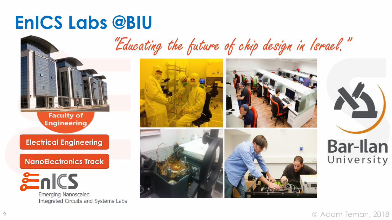
EnICS Labs @BIU
22
Electrical Engineering
NanoElectronics Track
“Educating the future of chip design in Israel.”

3 © Adam Teman, 2018
Lecture Outline

Motivation and Introduction
1
Motivation
2
Building a
Chip
3
Design
Automation
4
Chip Design
Flow

© Adam Teman, 2018
Motivation
1964 – The Integrated Circuit
1971 – The Intel 4004
2,300 Transistors
1992 – The Intel 486DX21.2M Transistors
2006 – Itanium 2 “Montecito”
1.7B Transistors

© Adam Teman, 2018
Motivation
http://en.wikichip.org/wiki/intel/core_i7ee/i7-6950x
Core i7-6950X Extreme Edition (Broadwell-E)
Introduced May 2016
Technology 14nm FinFET
Memory 320KB L1-I$
320KB L1-D$
2.56MB L2$
25MB L3$
Cores 10
Threads 20
Frequency 3.0-3.5 GHz
Die Size 246 mm2
#Transistors 3.2 B

7 © Adam Teman, 2018
Motivation
• Houston, we have a problem…
10,000
1,000
100
10
1
0.1
0.01
0.001
Logic
tra
nsis
tors
per
chip
(in m
illio
ns)
100,000
10,000
1000
100
10
1
0.1
0.01
Pro
du
ctivity
(K)
Tra
ns./
Sta
ff-M
o.
IC capacity
productivity
Gap
“Moore’s Law of Engineers”

8 © Adam Teman, 2018
Motivation
• How on earth do we design such a thing???

© Adam Teman, 2018
The Solution:
9
Design
Abstraction
Design
Automation
Design
Re-use (IP)

10 © Adam Teman, 2018
Syllabus• Lecture 1: Introduction
• Lecture 2: Verilog
• Lecture 3: Logic Synthesis
• Lecture 4: Static Timing Analysis
• Lecture 5: Moving to the Physical Domain
• Lecture 6: Placement
• Lecture 7: Clock Tree Synthesis
• Lecture 8: Routing
• Lecture 9: I/O and Packaging
• Lecture 10: Design for Test

11 © Adam Teman, 2018
References
• Way too many to state all, and hopefully many are cited on the slides themselves, but here are a few:• Rob Rutenbar – “From Logic to Layout” (available on Coursera)
• Nir Sever – Low Power Design (BGU)
• Roy Shor – תכן לוגי (BGU)
• IDESA Digital Design Course
• Rabaey “Digital Integrated Circuits” 2nd Edition
• Weste, Harris “CMOS VLSI Design”
• Google (oh, thank you Google!)
• Cadence Support (support.cadence.com)
• Synopsys SolveNet (solvenet.synopsys.com)
• And many, many more…

Building a Chip
1
Motivation
2
Building a
Chip
3
Design
Automation
4
Chip Design
Flow

13 © Adam Teman, 2018
General Design Approach
• How do engineers build a bridge?
• Divide and conquer !!!!• Partition design problem into many sub-problems,
which are manageable• Define mathematical model for sub-problem
and find an algorithmic solution• Beware of model limitations and check them !!!!!!!
• Implement algorithm in individual design tools, define and implement general interfaces between the tools
• Implement checking tools for boundary conditions• Concatenate design tools to general design flows
which can be managed• See what doesn’t work and start over.
Partition
Model/Solution
Tools/Interfaces
Verify/Validate
Develop Flow

14 © Adam Teman, 2018
Basic Design Abstraction
System Level
Register Transfer Level
Gate Level
Transistor Level
Layout Level
Mask Level
Application
Algorithm
Programming Language
OS / Virtual Machine
Instruction Set Architecture
Microarchitecture
Register-Transfer Level
Circuits
Devices
Physics
Another view:

15 © Adam Teman, 2018
System Level Abstraction
• Abstract algorithmic description of high-level behavior • e.g., C-Programming language
• Abstract because it does not contain any implementation details for timing or data
• Efficient to get a compact execution model as a first design draft
• Difficult to maintain throughout project because no link to implementation
System Level
Register Transfer Level
Gate Level
Transistor Level
Layout Level
Mask Level
Port* compute_optimal_route_for_packet(Packet_t *packet, Channel_t *channel)
{static Queue_t *packet_queue;packet_queue = add_packet(packet_queue, packet);...
}

16 © Adam Teman, 2018
Register-Transfer Level (RTL)
• Cycle accurate model “close” to the hardware implementation• bit-vector data types and operations as abstraction from
bit-level implementation
• sequential constructs (e.g., if-then-else, while loops) to support modeling of complex control flow
System Level
Register Transfer Level
Gate Level
Transistor Level
Layout Level
Mask Level
module mark1;reg [31:0] m[0:8192];reg [12:0] pc;reg [31:0] acc;reg[15:0] ir;
alwaysbegin
ir = m[pc];if(ir[15:13] == 3b’000)
pc = m[ir[12:0]];else if (ir[15:13] == 3’b010)
acc = -m[ir[12:0]];...
endendmodule

17 © Adam Teman, 2018
Gate Level Abstraction (GTL)
• Model on finite-state machine level• Models function in Boolean logic using
registers and gates
• Various delay models for gates and wires
System Level
Register Transfer Level
Gate Level
Transistor Level
Layout Level
Mask Level
4ns3ns
5ns
18 © Adam Teman, 2018
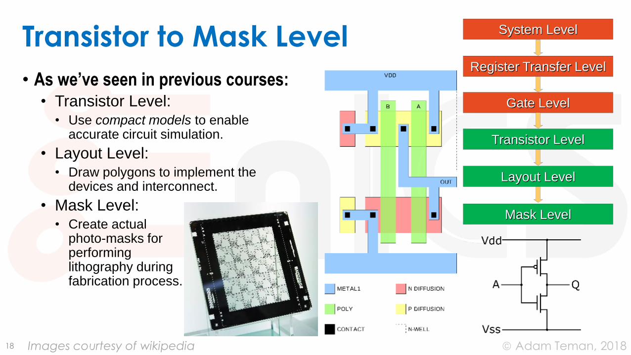
Transistor to Mask Level
• As we’ve seen in previous courses:• Transistor Level:
• Use compact models to enable accurate circuit simulation.
• Layout Level: • Draw polygons to implement the
devices and interconnect.
• Mask Level:• Create actual
photo-masks for performing lithography during fabrication process.
System Level
Register Transfer Level
Gate Level
Transistor Level
Layout Level
Mask Level
Images courtesy of wikipedia

The Chip Hall of Fame
• To get started, let’s remember the CPU that started it all
• The first commercially available monotlithic CPU.
• Release date: March 1971
• Transistor Count: 2,300 Process: 10 um pMOS
• Frequency: 740 KHz 4-bit data bus
• Designed as a side project to drum up some cash, while Intel developed its real product line, memory chips.
• Developed as part of a 4-chip product line (MCS-4 chipset) for the Busicom calculator.
2018 Inductee to the IEEE Chip Hall of Fame wikipedia
Federico Faggin and
the 4004 layout
IEEE Spectrum
The Busicom Calculator
IEEE Spectrum

Design Automation
1
Motivation
2
Building a
Chip
3
Design
Automation
4
Chip Design
Flow

21 © Adam Teman, 2018
The (really) Olden Days• Early chips were prepared entirely by hand:
Schematic of Intel 4004 (1971)
Mainframe CAD System (1967)
http://www.computerhistory.org/revolution/digital-logic

22 © Adam Teman, 2018
The (really) Olden Days• Early chips were prepared entirely by hand:
Hand drawn gate layout (Fairchild)
8088A Mask Transparent Overlays (1976)
Rubylith Operators (1970) The original Tape-Out?
http://www.computerhistory.org/revolution/digital-logic

23 © Adam Teman, 2018
Design Automation Today
Design:• High-Level Synthesis
• Logic Synthesis
• Schematic Capture
• Layout
• PCB Design
Simulation:• Transistor Simulation
• Logic Simulation
• Hardware Emulation
• Technology CAD
• Field Solvers
Analysis and Verification:• Functional Verification• Clock Domain Crossing• Formal Verification• Equivalence Checking• Static Timing Analysis• Physical Verification
Validation:• ATPG
• BIST
Mask Preparation:• Optical Proximity Correction (OPC)
• Resolution Enhancement Techniques
• Mask Generation
24 © Adam Teman, 2018
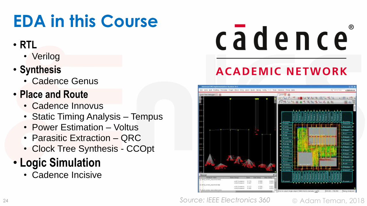
EDA in this Course
• RTL• Verilog
• Synthesis• Cadence Genus
• Place and Route• Cadence Innovus• Static Timing Analysis – Tempus• Power Estimation – Voltus• Parasitic Extraction – QRC• Clock Tree Synthesis - CCOpt
• Logic Simulation• Cadence Incisive
Source: IEEE Electronics 360

Chip Design Flow
1
Motivation
2
Building a
Chip
3
Design
Automation
4
Chip Design
Flow

26 © Adam Teman, 2018
How a chip is built
• Definition and Planning
• Design and Verification (Frontend)
• Logic Synthesis (Frontend and Backend)
• Physical Design (Backend)
• Signoff and Tapeout
• Silicon Validation
• Don’t forget package & board design, software design, test plan, etc., etc., etc.
Definition and Planning
Design and Verification
Logic Synthesis
Physical Design
Signoff and Tapeout
Silicon Validation

27 © Adam Teman, 2018
Definition & Planning
• Marketing Requirements Document (MRD)
• Chip Architecture• Define bus structures, connectivity
• Partition Functionality
• High-Level System Model (Bandwidths, Power, Freq.)
• System partitioning (HW vs SW, #Cores, Memories…)
• Design Documents
• Floorplan/Board Requirements
• Process and fab
• Project kick-off – transfer to implementation
Definition and Planning
Design and Verification
Logic Synthesis
Physical Design
Signoff and Tapeout
Silicon Validation

28 © Adam Teman, 2018
Design and Verification
• RTL (Register Transfer Level) Design
• Integration/Development of IPs
• RTL Lint/Synthesability checks
• Formal Verification
• Functional verification all the IPs: • Unit level
• Sub-system level
• Chip (SOC) level
Definition and Planning
Design and Verification
Logic Synthesis
Physical Design
Signoff and Tapeout
Silicon Validation

29 © Adam Teman, 2018
Design and Verification - IP Integration
• Hard IP• IP provided as pre-existing layouts with:
• Timing models
• Layout abstracts
• Behavioral models (Verilog/VHDL)
• Sometimes with Spice models, full-layouts
• This is the standard delivery format for custom digital blocks• RAMs, ROMs, PLLs, Processors
• Soft IP• RTL Code
• Can be encrypted
• Instantiated just like any other RTL block
• Sometimes with behavioral models
Definition and Planning
Design and Verification
Logic Synthesis
Physical Design
Signoff and Tapeout
Silicon Validation
30 © Adam Teman, 2018
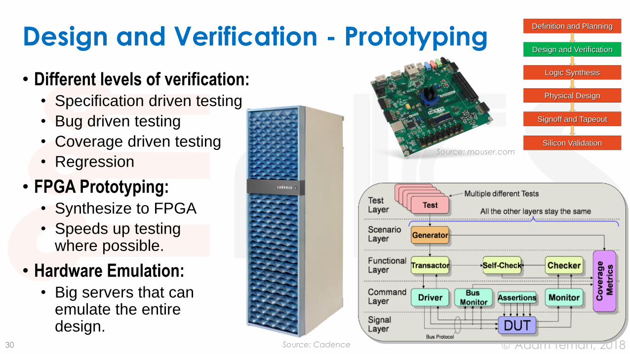
Design and Verification - Prototyping
• Different levels of verification:• Specification driven testing
• Bug driven testing
• Coverage driven testing
• Regression
• FPGA Prototyping:• Synthesize to FPGA
• Speeds up testing where possible.
• Hardware Emulation:• Big servers that can
emulate the entire design.
Definition and Planning
Design and Verification
Logic Synthesis
Physical Design
Signoff and Tapeout
Silicon ValidationSource: mouser.com
Source: Cadence

31 © Adam Teman, 2018
• Synthesis• Converting RTL code into a generic logic
netlist
• Mapping• Mapping generic netlist into standard cells
from the core library
• Optimization• To meet Timing / Area / Power constraints
Logic Synthesis
• Inputs:
• Technology library file
• RTL files
• Constraint files (SDC)
• DFT definitions
• Output:
• Gate-level netlist
Definition and Planning
Design and Verification
Logic Synthesis
Physical Design
Signoff and Tapeout
Silicon Validation
module DFF(Clk, D, Q);
input Clk;
input D;
output Q;
always @(posedge Clk)
Q <= D;
endmoduleClk
D Q • Post Synthesis checks• Gate-level simulation
• Formal verification (Logic Equivalence)
• Static Timing Analysis (STA)
• Power/Area estimation

32 © Adam Teman, 2018
Physical Design (Backend)
• Floorplan
• I/O Ring
• Power Plan
• Placement
• Clock Tree Synthesis
• Route
• DRC, LVS, Antennas, EM
• LEC, Post-layout
Definition and Planning
Design and Verification
Logic Synthesis
Physical Design
Signoff and Tapeout
Silicon Validation
33 © Adam Teman, 2018
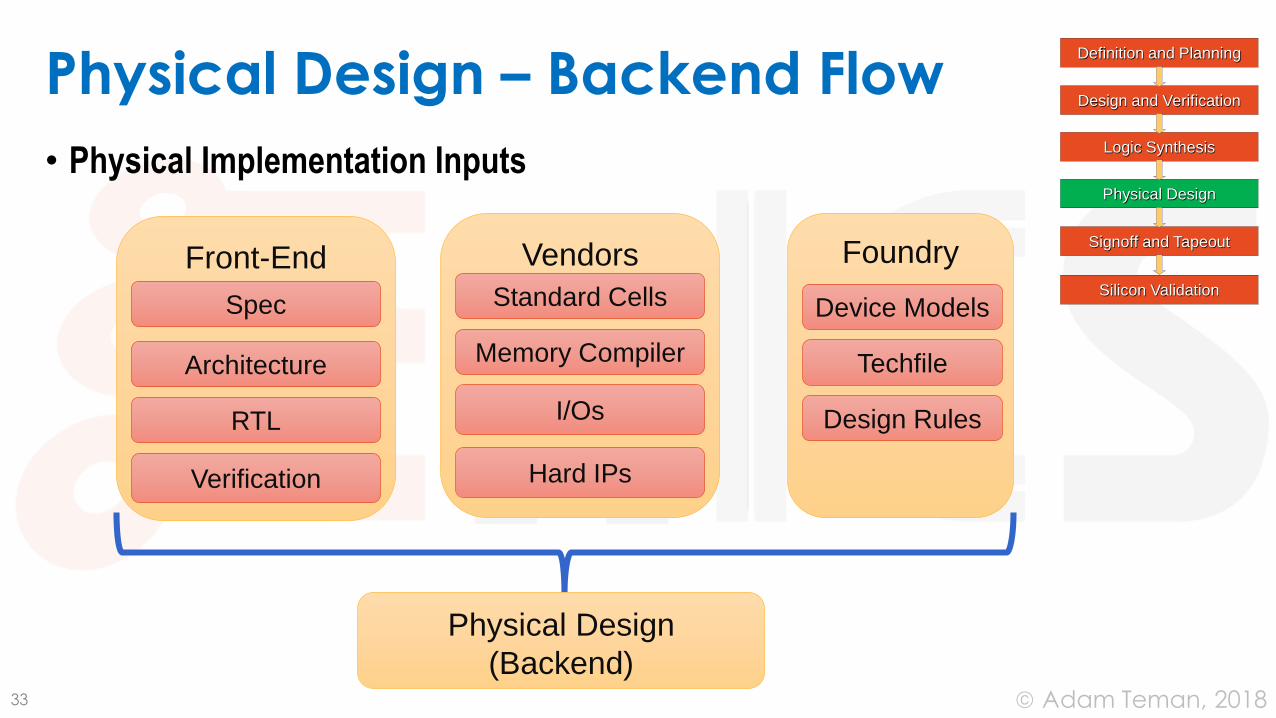
Physical Design – Backend Flow
• Physical Implementation Inputs
Definition and Planning
Design and Verification
Logic Synthesis
Physical Design
Signoff and Tapeout
Silicon Validation
Foundry
Device Models
Techfile
Design Rules
Vendors
Standard Cells
Memory Compiler
I/Os
Hard IPs
Front-End
Architecture
RTL
Verification
Physical Design
(Backend)
Spec

© Adam Teman, 2018
Physical Design – Backend Flow
SynthesizerRTL
SDC
Standard Cells and
Macros
Gate Level
ATPG
Scan Chains
GTL with Scan
Placer
Floorplan
Power Grid,
Special Routing
Placed Design
CTSDesign with
Clock Tree
Clock Definitions
Router Routed Design
Extraction, STA, DRC,
LVS, Density, Antennas,
Caps, Power/EM
GDSII
Definition and Planning
Design and Verification
Logic Synthesis
Physical Design
Signoff and Tapeout
Silicon Validation

35 © Adam Teman, 2018
Signoff and Tapeout
• Parasitic Extraction
• STA with SI
• DRC/LVS/ERC/DFM
• Post-layout Gate-level Simulation
• Power Analysis
• DFT
• Logic Equivalence
Definition and Planning
Design and Verification
Logic Synthesis
Physical Design
Signoff and Tapeout
Silicon Validation

36 © Adam Teman, 2018
Glossary
• Just to cover most of the terminology of today’s lesson:
• RTL
• GTL
• CAD
• EDA
• DFT (ATPG, Scan, BIST)
• OPC
• Frontend
• Backend
• Verification
• Signoff
• Tapeout
• Hard IP
• Soft IP
• FPGA
• Emulation
• Lint
• Formal Verification
• STA
• SDC
• SI
• DRC, LVS, EM
• GDSII
Special Thanks to:
Nir Sever
IDESA Digital Course
Marvell Israel
For the knowledge and materials
required for preparing this lecture.