
Digital PMR Radio Processor - cmlmicro.com€¦ · Digital PMR Radio Processor CMX7131/CMX7141 2013...
69
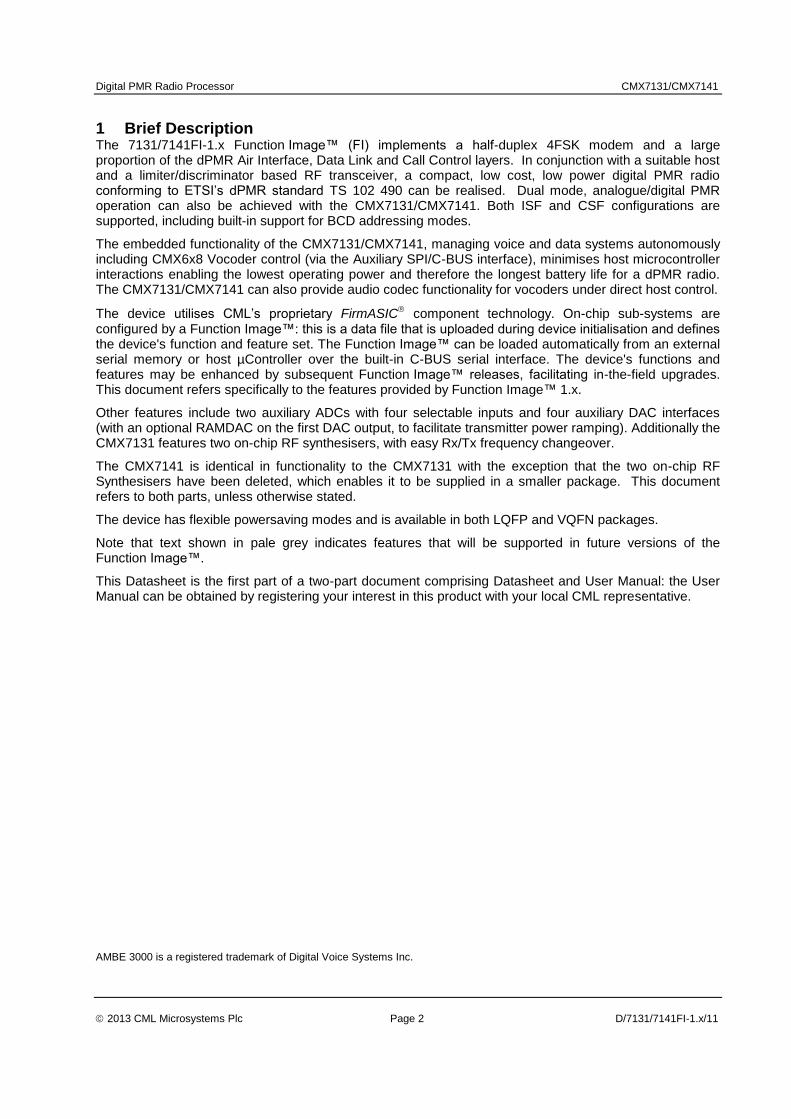
CML Microcircuits COMMUNICATION SEMICONDUCTORS CMX7131/CMX7141 Digital PMR Processor dPMR 2013 CML Microsystems Plc D/7131/7141FI-1.x/11 October 2013 DATASHEET Provisional Information 7131/7141FI-1.x: dPMR Baseband Data Processor with Auxiliary System Clocks, ADCs and DACs Features Digital PMR dPMR (ETSI TS 102 490) Compliant Air Interface Physical Layer (Layer 1) Air Interface Data Link Layer (Layer 2) Supports similar functionality to I 2 S Mode 2 Auxiliary ADCs (4 Multiplexed Inputs) 4 Auxiliary DACs 2 Auxiliary System Clock Outputs Tx Outputs for Two Point or I/Q Modulation Flexible Powersave Modes 4FSK Modem 4.8 and 9.6 kbps Data Rates Soft-decision Data Output Option AFSD (Automated Frame Sync Detection) Raw Data Mode Available in Small LQFP or VQFN Packages Low-power (3.3V) Operation C-BUS Serial Interface to Host μController Two RF Synthesisers (CMX7131 only) Vocoder Connectivity o Vocoder Management and Control (RALCWI Vocoders CMX608 and CMX618) o Vocoder Data Transport (Third-party Vocoders e.g. AMBE3000) CMX7131 CMX7141 Digital PMR Processor Modulator RF Discriminator Host μC System clock 1 System clock 2 RALCWI Vocoder CMX608 CMX618 Reference clock DAC outputs ADC inputs 3.3V Built on FirmASIC ® Technology GPIO Tx enable Rx enable Tx PA ramp RF Synthesiser 1 RF Synthesiser 2 CMX7131 only Third-Party Vocoder
Transcript of Digital PMR Radio Processor - cmlmicro.com€¦ · Digital PMR Radio Processor CMX7131/CMX7141 2013...

CML Microcircuits
COMMUNICATION SEMICONDUCTORS
CMX7131/CMX7141 Digital PMR Processor
dPMR
2013 CML Microsystems Plc
D/7131/7141FI-1.x/11 October 2013 DATASHEET Provisional Information
7131/7141FI-1.x: dPMR Baseband Data Processor with Auxiliary System Clocks,
ADCs and DACs
Features
Digital PMR
dPMR (ETSI TS 102 490) Compliant
Air Interface Physical Layer (Layer 1)
Air Interface Data Link Layer (Layer 2)
Supports similar functionality to I2S Mode
2 Auxiliary ADCs (4 Multiplexed Inputs)
4 Auxiliary DACs
2 Auxiliary System Clock Outputs
Tx Outputs for Two Point or I/Q Modulation
Flexible Powersave Modes
4FSK Modem
4.8 and 9.6 kbps Data Rates
Soft-decision Data Output Option
AFSD (Automated Frame Sync Detection)
Raw Data Mode
Available in Small LQFP or VQFN Packages
Low-power (3.3V) Operation
C-BUS Serial Interface to Host µController
Two RF Synthesisers (CMX7131 only)
Vocoder Connectivity
o Vocoder Management and Control (RALCWI Vocoders CMX608 and CMX618)
o Vocoder Data Transport (Third-party Vocoders e.g. AMBE3000)
CMX7131
CMX7141Digital PMR
Processor
Modulator
RF
Discriminator
Host µC
System clock 1System clock 2
RALCWI
Vocoder
CMX608
CMX618
Reference clock
DAC outputs
ADC inputs
3.3V
Built on FirmASIC® Technology
GPIO
Tx enable
Rx enable
Tx PA ramp
RF Synthesiser 1
RF Synthesiser 2
CMX7131 only
Third-Party
Vocoder
kbennion
ds
Digital PMR Radio Processor CMX7131/CMX7141
2013 CML Microsystems Plc Page 2 D/7131/7141FI-1.x/11
1 Brief Description The 7131/7141FI-1.x Function Image™ (FI) implements a half-duplex 4FSK modem and a large proportion of the dPMR Air Interface, Data Link and Call Control layers. In conjunction with a suitable host and a limiter/discriminator based RF transceiver, a compact, low cost, low power digital PMR radio conforming to ETSI’s dPMR standard TS 102 490 can be realised. Dual mode, analogue/digital PMR operation can also be achieved with the CMX7131/CMX7141. Both ISF and CSF configurations are supported, including built-in support for BCD addressing modes.
The embedded functionality of the CMX7131/CMX7141, managing voice and data systems autonomously including CMX6x8 Vocoder control (via the Auxiliary SPI/C-BUS interface), minimises host microcontroller interactions enabling the lowest operating power and therefore the longest battery life for a dPMR radio. The CMX7131/CMX7141 can also provide audio codec functionality for vocoders under direct host control.
The device utilises CML’s proprietary FirmASIC component technology. On-chip sub-systems are configured by a Function Image™: this is a data file that is uploaded during device initialisation and defines the device's function and feature set. The Function Image™ can be loaded automatically from an external serial memory or host µController over the built-in C-BUS serial interface. The device's functions and features may be enhanced by subsequent Function Image™ releases, facilitating in-the-field upgrades. This document refers specifically to the features provided by Function Image™ 1.x.
Other features include two auxiliary ADCs with four selectable inputs and four auxiliary DAC interfaces (with an optional RAMDAC on the first DAC output, to facilitate transmitter power ramping). Additionally the CMX7131 features two on-chip RF synthesisers, with easy Rx/Tx frequency changeover.
The CMX7141 is identical in functionality to the CMX7131 with the exception that the two on-chip RF Synthesisers have been deleted, which enables it to be supplied in a smaller package. This document refers to both parts, unless otherwise stated.
The device has flexible powersaving modes and is available in both LQFP and VQFN packages.
Note that text shown in pale grey indicates features that will be supported in future versions of the Function Image™.
This Datasheet is the first part of a two-part document comprising Datasheet and User Manual: the User Manual can be obtained by registering your interest in this product with your local CML representative.
AMBE 3000 is a registered trademark of Digital Voice Systems Inc.
Digital PMR Radio Processor CMX7131/CMX7141
2013 CML Microsystems Plc Page 3 D/7131/7141FI-1.x/11
CONTENTS
Section Page
1 Brief Description ...................................................................................................................... 2
2 Block Diagram .......................................................................................................................... 8
3 Signal List ................................................................................................................................. 9 3.1 Signal Definitions ........................................................................................................ 11
4 External Components............................................................................................................ 12 4.1 Recommended External Components ....................................................................... 14
5 PCB Layout Guidelines and Power Supply Decoupling .................................................... 15
6 General Description ............................................................................................................... 17 6.1 7131/7141 FI-1.x Features ......................................................................................... 17 6.2 System Design ............................................................................................................ 18
6.2.1 Implementation using the CMX6x8 ...................................................................... 18 6.2.2 Implementing with Third-party Vocoders .............................................................. 19 6.2.3 Data Transfer ....................................................................................................... 21 6.2.4 RSSI Measurement .............................................................................................. 21 6.2.5 Serial Memory Connection ................................................................................... 21
6.3 Introduction ................................................................................................................. 21 6.3.1 Modulation ............................................................................................................ 21 6.3.2 Internal Data Processing ...................................................................................... 23 6.3.3 Frame Sync Detection and Demodulation ........................................................... 24 6.3.4 FEC and Coding ................................................................................................... 27 6.3.5 Voice Coding ........................................................................................................ 27 6.3.6 Radio Performance Requirements ....................................................................... 27
7 Detailed Descriptions ............................................................................................................ 28 7.1 Xtal Frequency ............................................................................................................ 28 7.2 Host Interface ............................................................................................................. 28
7.2.1 C-BUS Operation ................................................................................................. 28 7.3 Function Image™ Loading.......................................................................................... 30
7.3.1 FI Loading from Host Controller ........................................................................... 30 7.3.2 FI Loading from Serial Memory ............................................................................ 32
7.4 CMX618/CMX608 Interface ........................................................................................ 33 7.5 DVSI Vocoder Interface .............................................................................................. 35
7.5.1 Support for I2S Mode ............................................................................................ 35
7.6 Device Control ............................................................................................................ 35 7.6.1 General Notes ...................................................................................................... 36 7.6.2 Interrupt Operation ............................................................................................... 36 7.6.3 Signal Routing ...................................................................................................... 36 7.6.4 Modem Control ..................................................................................................... 37 7.6.5 Tx Mode (Raw) ..................................................................................................... 38 7.6.6 Tx Mode (PRBS) .................................................................................................. 38 7.6.7 Tx Sequencer ....................................................................................................... 40 7.6.8 Rx Mode (Raw) .................................................................................................... 40 7.6.9 Other Modem Modes ........................................................................................... 41
Digital PMR Radio Processor CMX7131/CMX7141
2013 CML Microsystems Plc Page 4 D/7131/7141FI-1.x/11
7.6.10 Reset/Abort .......................................................................................................... 42 7.6.11 Data Transfer ....................................................................................................... 42 7.6.12 CMX6x8 Pass-through Mode ............................................................................... 42
7.7 dPMR Formatted Operation ....................................................................................... 43 7.7.1 Operating Modes and Addressing ........................................................................ 43 7.7.2 ISF Addressing ..................................................................................................... 44 7.7.3 CSF Addressing ................................................................................................... 44 7.7.4 Tx Mode (dPMR formatted) ................................................................................. 44 7.7.5 Rx Mode (dPMR formatted) ................................................................................. 46 7.7.6 Slow Data ............................................................................................................. 47
7.8 Squelch Operation ...................................................................................................... 47 7.9 GPIO Pin Operation .................................................................................................... 47 7.10 Auxiliary ADC Operation ............................................................................................. 48 7.11 Auxiliary DAC/RAMDAC Operation ............................................................................ 49 7.12 RF Synthesiser (CMX7131 only) ................................................................................ 49 7.13 Digital System Clock Generators ................................................................................ 53
7.13.1 Main Clock Operation ........................................................................................... 53 7.13.2 System Clock Operation ...................................................................................... 54
7.14 Signal Level Optimisation ........................................................................................... 54 7.14.1 Transmit Path Levels ........................................................................................... 54 7.14.2 Receive Path Levels............................................................................................. 54
7.15 Tx Spectrum Plots ...................................................................................................... 55 7.16 C-BUS Register Summary .......................................................................................... 56
8 Performance Specification ................................................................................................... 57 8.1 Electrical Performance ............................................................................................... 57
8.1.1 Absolute Maximum Ratings ................................................................................. 57 8.1.2 Operating Limits ................................................................................................... 58 8.1.3 Operating Characteristics ..................................................................................... 59 8.1.4 Parametric Performance ...................................................................................... 65
8.2 C-BUS Timing ............................................................................................................. 66 8.3 Packaging ................................................................................................................... 67
Table Page
Table 1 Definition of Power Supply and Reference Voltages ........................................................ 11 Table 2 dPMR Frame Format - Call set-up, no ACK .................................................................... 25 Table 3 dPMR Frame Format - Call set-up with ACK ................................................................... 25 Table 4 Xtal/Clock Frequency Settings for Program Block 3 ........................................................ 28 Table 5 BOOTEN Pin States ......................................................................................................... 30 Table 6 CMX6x8 Vocoder Connections ........................................................................................ 33 Table 7 DVSI Vocoder Connections ............................................................................................. 35 Table 8 Modem Mode Selection ................................................................................................... 37 Table 9 Modem Control Selection ................................................................................................. 38 Table 10 C-BUS Data Registers ................................................................................................... 42 Table 11 C-BUS Registers ............................................................................................................ 56
Figure Page
Figure 1 Block Diagram ................................................................................................................... 8
Digital PMR Radio Processor CMX7131/CMX7141
2013 CML Microsystems Plc Page 5 D/7131/7141FI-1.x/11
Figure 2 CMX7141 Recommended External Components ........................................................... 12 Figure 3 CMX7131 Recommended External Components ........................................................... 13 Figure 4 CMX7141 Power Supply and De-coupling ...................................................................... 15 Figure 5 CMX7131 Power Supply and De-coupling ...................................................................... 16 Figure 6 CMX618 Vocoder Connection ........................................................................................ 19 Figure 7 CMX608 Vocoder Connection ........................................................................................ 19 Figure 8 DVSI Vocoder Connection .............................................................................................. 20 Figure 9 Dual Vocoder Connection ............................................................................................... 20 Figure 10 4FSK PRBS Waveform - Modulation ............................................................................ 22 Figure 11 4FSK PRBS Waveform - Spectrum .............................................................................. 22 Figure 12 dPMR Modulation Characteristics ................................................................................. 23 Figure 13 Internal Data Processing Blocks ................................................................................... 24 Figure 14 FS Detection ................................................................................................................. 26 Figure 15 C-BUS Transactions ..................................................................................................... 29 Figure 16 FI Loading from Host .................................................................................................... 31 Figure 17 FI Loading from Serial Memory ..................................................................................... 32 Figure 18 Digital Voice Rx and Tx Blocks ..................................................................................... 34 Figure 19 I
2S Mode Support .......................................................................................................... 35
Figure 20 Tx Data Flow (Raw Data Mode) .................................................................................... 39 Figure 21 Automatic Tx Sequencer ............................................................................................... 40 Figure 22 Rx Data Flow (Raw Data Mode) ................................................................................... 41 Figure 23 AuxADC IRQ Operation ................................................................................................ 48 Figure 24 Example RF Synthesiser Components ......................................................................... 50 Figure 25 Single RF Synthesiser Block Diagram .......................................................................... 50 Figure 26 Digital Clock Generation Schemes ............................................................................... 53 Figure 27 Tx Modulation Spectra - 4800bps ................................................................................. 55 Figure 28 Tx Modulation Spectra - 9600bps ................................................................................. 55 Figure 29 C-BUS Timing ............................................................................................................... 66 Figure 30 Mechanical Outline of 64-pin VQFN (Q1) ..................................................................... 67 Figure 31 Mechanical Outline of 64-pin LQFP (L9) ....................................................................... 67 Figure 32 Mechanical Outline of 48-pin LQFP (L4) ....................................................................... 68 Figure 33 Mechanical Outline of 48-pin VQFN (Q3) ..................................................................... 68
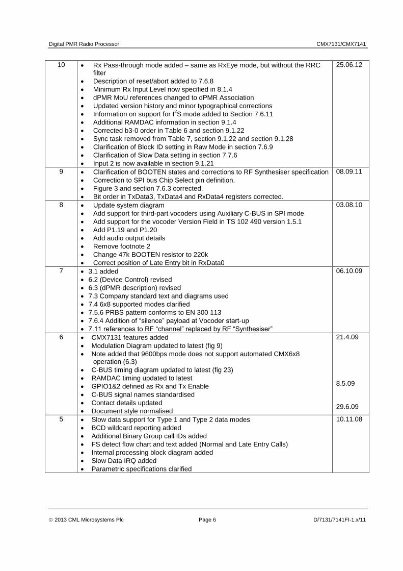
History
Version Changes Date
11 Updated RAMDAC and tone generator descriptions
Various typographical and editorial changes and update to version history.
01.10.13
Digital PMR Radio Processor CMX7131/CMX7141
2013 CML Microsystems Plc Page 6 D/7131/7141FI-1.x/11
10 Rx Pass-through mode added – same as RxEye mode, but without the RRC filter
Description of reset/abort added to 7.6.8
Minimum Rx Input Level now specified in 8.1.4
dPMR MoU references changed to dPMR Association
Updated version history and minor typographical corrections
Information on support for I2S mode added to Section 7.6.11
Additional RAMDAC information in section 9.1.4
Corrected b3-0 order in Table 6 and section 9.1.22
Sync task removed from Table 7, section 9.1.22 and section 9.1.28
Clarification of Block ID setting in Raw Mode in section 7.6.9
Clarification of Slow Data setting in section 7.7.6
Input 2 is now available in section 9.1.21
25.06.12
9 Clarification of BOOTEN states and corrections to RF Synthesiser specification
Correction to SPI bus Chip Select pin definition.
Figure 3 and section 7.6.3 corrected.
Bit order in TxData3, TxData4 and RxData4 registers corrected.
08.09.11
8 Update system diagram
Add support for third-part vocoders using Auxiliary C-BUS in SPI mode
Add support for the vocoder Version Field in TS 102 490 version 1.5.1
Add P1.19 and P1.20
Add audio output details
Remove footnote 2
Change 47k BOOTEN resistor to 220k
Correct position of Late Entry bit in RxData0
03.08.10
7 3.1 added
6.2 (Device Control) revised
6.3 (dPMR description) revised
7.3 Company standard text and diagrams used
7.4 6x8 supported modes clarified
7.5.6 PRBS pattern conforms to EN 300 113
7.6.4 Addition of “silence” payload at Vocoder start-up
7.11 references to RF “channel” replaced by RF “Synthesiser”
06.10.09
6 CMX7131 features added
Modulation Diagram updated to latest (fig 9)
Note added that 9600bps mode does not support automated CMX6x8 operation (6.3)
C-BUS timing diagram updated to latest (fig 23)
RAMDAC timing updated to latest
GPIO1&2 defined as Rx and Tx Enable
C-BUS signal names standardised
Contact details updated
Document style normalised
21.4.09 8.5.09 29.6.09
5 Slow data support for Type 1 and Type 2 data modes
BCD wildcard reporting added
Additional Binary Group call IDs added
FS detect flow chart and text added (Normal and Late Entry Calls)
Internal processing block diagram added
Slow Data IRQ added
Parametric specifications clarified
10.11.08
Digital PMR Radio Processor CMX7131/CMX7141
2013 CML Microsystems Plc Page 7 D/7131/7141FI-1.x/11
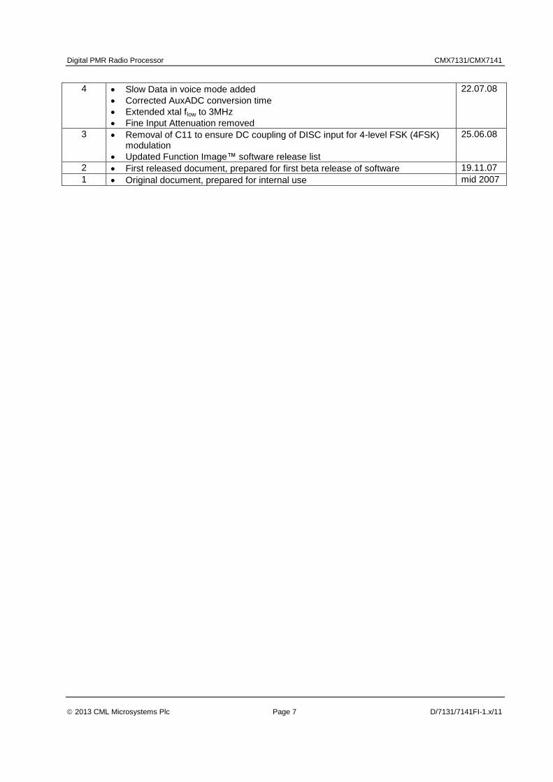
4 Slow Data in voice mode added
Corrected AuxADC conversion time
Extended xtal flow to 3MHz
Fine Input Attenuation removed
22.07.08
3 Removal of C11 to ensure DC coupling of DISC input for 4-level FSK (4FSK) modulation
Updated Function Image™ software release list
25.06.08
2 First released document, prepared for first beta release of software 19.11.07
1 Original document, prepared for internal use mid 2007
Digital PMR Radio Processor CMX7131/CMX7141
2013 CML Microsystems Plc Page 8 D/7131/7141FI-1.x/11
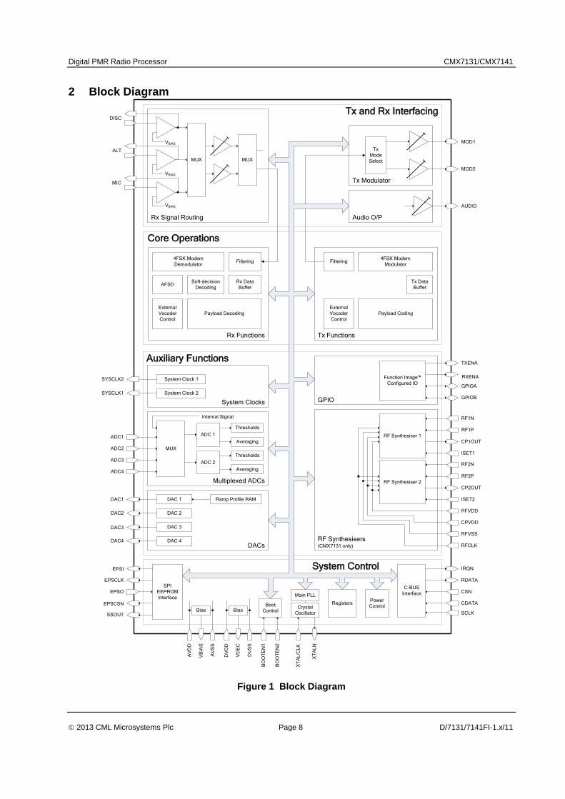
2 Block Diagram
ALT
TXENA
RXENA
GPIOA
GPIOB
MOD2
ADC1
ADC2
ADC3
ADC4
EPSCLK
BO
OT
EN
1
BO
OT
EN
2
EPSCSN
SYSCLK1
SYSCLK2
AV
DD
VB
IAS
AV
SS
XT
AL
/CL
K
XT
AL
N
EPSO
EPSI
Multiplexed ADCs
DACs
System Clocks
System Control
Internal Signal
MUX
Function Image™
Configured IO
MUX
ADC 1
Thresholds
Averaging
Thresholds
Averaging
System Clock 1
System Clock 2
C-BUS
Interface
IRQN
RDATA
SCLK
Power
ControlRegisters
SPI
EEPROM
Interface
Bias
DV
DD
VD
EC
DV
SS
BiasCrystal
Oscillator
Boot
Control
Main PLL
Auxiliary Functions
ADC 2
Filtering4FSK Modem
Demodulator
CDATA
CSN
Tx
Mode
Select
GPIO
Rx Data
Buffer
VBIAS
VBIAS
MIC
Rx Signal Routing
MOD1
Tx Modulator
VBIAS
DISC
SSOUT
Filtering
Tx Data
Buffer
AUDIO
MUX
Core Operations
Tx and Rx Interfacing
Audio O/P
AFSDSoft-decision
Decoding
Payload Decoding
4FSK Modem
Modulator
Payload Coding
Rx Functions Tx Functions
External
Vocoder
Control
External
Vocoder
Control
DAC1
DAC2
DAC3
DAC4
DAC 1
DAC 2
DAC 3
DAC 4
Ramp Profile RAM
RF Synthesiser 1
RF Synthesiser 2
RF1N
CP1OUT
ISET1
RF2N
CP2OUT
ISET2
RFVDD
CPVDD
RFVSS
RFCLK
RF Synthesisers(CMX7131 only)
RF1P
RF2P
Figure 1 Block Diagram
Digital PMR Radio Processor CMX7131/CMX7141
2013 CML Microsystems Plc Page 9 D/7131/7141FI-1.x/11
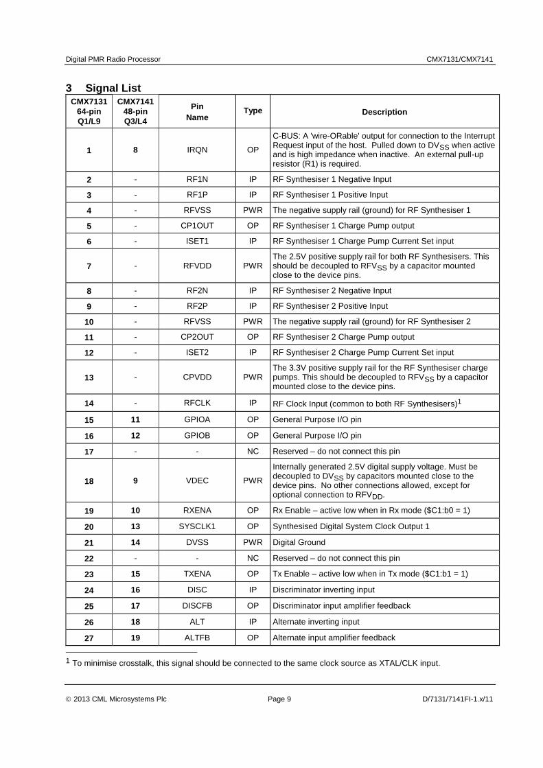
3 Signal List CMX7131
64-pin
Q1/L9
CMX7141
48-pin
Q3/L4
Pin
Name Type Description
1 8 IRQN OP
C-BUS: A 'wire-ORable' output for connection to the Interrupt Request input of the host. Pulled down to DVSS when active and is high impedance when inactive. An external pull-up resistor (R1) is required.
2 - RF1N IP RF Synthesiser 1 Negative Input
3 - RF1P IP RF Synthesiser 1 Positive Input
4 - RFVSS PWR The negative supply rail (ground) for RF Synthesiser 1
5 - CP1OUT OP RF Synthesiser 1 Charge Pump output
6 - ISET1 IP RF Synthesiser 1 Charge Pump Current Set input
7 - RFVDD PWR The 2.5V positive supply rail for both RF Synthesisers. This should be decoupled to RFVSS by a capacitor mounted close to the device pins.
8 - RF2N IP RF Synthesiser 2 Negative Input
9 - RF2P IP RF Synthesiser 2 Positive Input
10 - RFVSS PWR The negative supply rail (ground) for RF Synthesiser 2
11 - CP2OUT OP RF Synthesiser 2 Charge Pump output
12 - ISET2 IP RF Synthesiser 2 Charge Pump Current Set input
13 - CPVDD PWR The 3.3V positive supply rail for the RF Synthesiser charge pumps. This should be decoupled to RFVSS by a capacitor mounted close to the device pins.
14 - RFCLK IP RF Clock Input (common to both RF Synthesisers)1
15 11 GPIOA OP General Purpose I/O pin
16 12 GPIOB OP General Purpose I/O pin
17 - - NC Reserved – do not connect this pin
18 9 VDEC PWR
Internally generated 2.5V digital supply voltage. Must be decoupled to DVSS by capacitors mounted close to the device pins. No other connections allowed, except for optional connection to RFVDD.
19 10 RXENA OP Rx Enable – active low when in Rx mode ($C1:b0 = 1)
20 13 SYSCLK1 OP Synthesised Digital System Clock Output 1
21 14 DVSS PWR Digital Ground
22 - - NC Reserved – do not connect this pin
23 15 TXENA OP Tx Enable – active low when in Tx mode ($C1:b1 = 1)
24 16 DISC IP Discriminator inverting input
25 17 DISCFB OP Discriminator input amplifier feedback
26 18 ALT IP Alternate inverting input
27 19 ALTFB OP Alternate input amplifier feedback
1 To minimise crosstalk, this signal should be connected to the same clock source as XTAL/CLK input.
Digital PMR Radio Processor CMX7131/CMX7141
2013 CML Microsystems Plc Page 10 D/7131/7141FI-1.x/11
CMX7131
64-pin
Q1/L9
CMX7141
48-pin
Q3/L4
Pin
Name Type Description
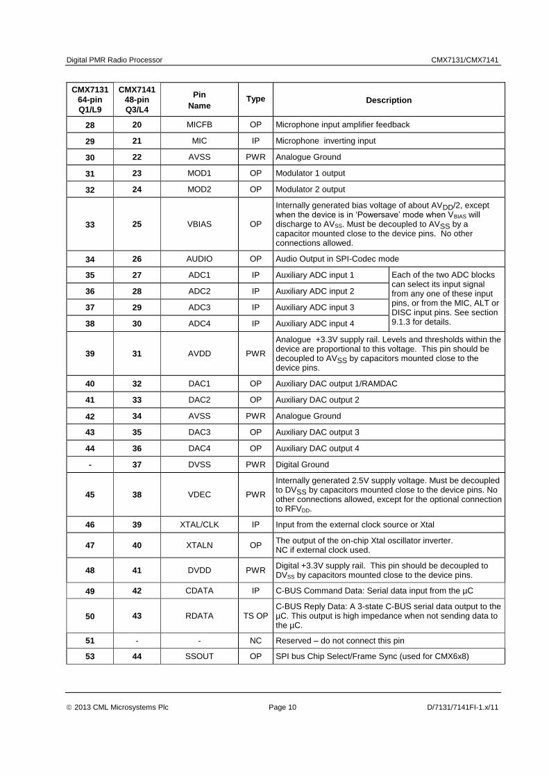
28 20 MICFB OP Microphone input amplifier feedback
29 21 MIC IP Microphone inverting input
30 22 AVSS PWR Analogue Ground
31 23 MOD1 OP Modulator 1 output
32 24 MOD2 OP Modulator 2 output
33 25 VBIAS OP
Internally generated bias voltage of about AVDD/2, except when the device is in ‘Powersave’ mode when VBIAS will discharge to AVSS. Must be decoupled to AVSS by a capacitor mounted close to the device pins. No other connections allowed.
34 26 AUDIO OP Audio Output in SPI-Codec mode
35 27 ADC1 IP Auxiliary ADC input 1 Each of the two ADC blocks can select its input signal from any one of these input pins, or from the MIC, ALT or DISC input pins. See section 9.1.3 for details.
36 28 ADC2 IP Auxiliary ADC input 2
37 29 ADC3 IP Auxiliary ADC input 3
38 30 ADC4 IP Auxiliary ADC input 4
39 31 AVDD PWR
Analogue +3.3V supply rail. Levels and thresholds within the device are proportional to this voltage. This pin should be decoupled to AVSS by capacitors mounted close to the device pins.
40 32 DAC1 OP Auxiliary DAC output 1/RAMDAC
41 33 DAC2 OP Auxiliary DAC output 2
42 34 AVSS PWR Analogue Ground
43 35 DAC3 OP Auxiliary DAC output 3
44 36 DAC4 OP Auxiliary DAC output 4
- 37 DVSS PWR Digital Ground
45 38 VDEC PWR
Internally generated 2.5V supply voltage. Must be decoupled to DVSS by capacitors mounted close to the device pins. No other connections allowed, except for the optional connection to RFVDD.
46 39 XTAL/CLK IP Input from the external clock source or Xtal
47 40 XTALN OP The output of the on-chip Xtal oscillator inverter. NC if external clock used.
48 41 DVDD PWR Digital +3.3V supply rail. This pin should be decoupled to DVSS by capacitors mounted close to the device pins.
49 42 CDATA IP C-BUS Command Data: Serial data input from the µC
50 43 RDATA TS OP C-BUS Reply Data: A 3-state C-BUS serial data output to the µC. This output is high impedance when not sending data to the µC.
51 - - NC Reserved – do not connect this pin
53 44 SSOUT OP SPI bus Chip Select/Frame Sync (used for CMX6x8)
Digital PMR Radio Processor CMX7131/CMX7141
2013 CML Microsystems Plc Page 11 D/7131/7141FI-1.x/11
CMX7131
64-pin
Q1/L9
CMX7141
48-pin
Q3/L4
Pin
Name Type Description
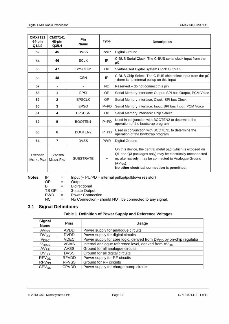
52 45 DVSS PWR Digital Ground
54 46 SCLK IP C-BUS Serial Clock: The C-BUS serial clock input from the µC
55 47 SYSCLK2 OP Synthesised Digital System Clock Output 2
56 48 CSN IP C-BUS Chip Select: The C-BUS chip select input from the µC - there is no internal pullup on this input
57 - - NC Reserved – do not connect this pin
58 1 EPSI OP Serial Memory Interface: Output; SPI bus Output, PCM Voice
59 2 EPSCLK OP Serial Memory Interface: Clock; SPI bus Clock
60 3 EPSO IP+PD Serial Memory Interface: Input; SPI bus Input, PCM Voice
61 4 EPSCSN OP Serial Memory Interface: Chip Select
62 5 BOOTEN1 IP+PD Used in conjunction with BOOTEN2 to determine the operation of the bootstrap program
63 6 BOOTEN2 IP+PD Used in conjunction with BOOTEN1 to determine the operation of the bootstrap program
64 7 DVSS PWR Digital Ground
EXPOSED
METAL PAD
EXPOSED
METAL PAD SUBSTRATE ~
On this device, the central metal pad (which is exposed on
Q1 and Q3 packages only) may be electrically unconnected
or, alternatively, may be connected to Analogue Ground
(AVSS).
No other electrical connection is permitted.
Notes: IP = Input (+ PU/PD = internal pullup/pulldown resistor) OP = Output BI = Bidirectional TS OP = 3-state Output PWR = Power Connection NC = No Connection - should NOT be connected to any signal.
3.1 Signal Definitions
Table 1 Definition of Power Supply and Reference Voltages
Signal
Name Pins Usage
AVDD AVDD Power supply for analogue circuits
DVDD DVDD Power supply for digital circuits
VDEC VDEC Power supply for core logic, derived from DVDD by on-chip regulator
VBIAS VBIAS Internal analogue reference level, derived from AVDD
AVSS AVSS Ground for all analogue circuits
DVSS DVSS Ground for all digital circuits
RFVDD RFVDD Power supply for RF circuits
RFVSS RFVSS Ground for RF circuits
CPVDD CPVDD Power supply for charge pump circuits

Digital PMR Radio Processor CMX7131/CMX7141
2013 CML Microsystems Plc Page 12 D/7131/7141FI-1.x/11
4 External Components
Figure 2 CMX7141 Recommended External Components
Digital PMR Radio Processor CMX7131/CMX7141
2013 CML Microsystems Plc Page 13 D/7131/7141FI-1.x/11
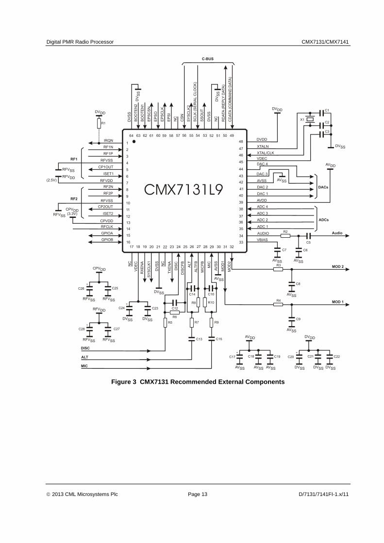
Figure 3 CMX7131 Recommended External Components
Digital PMR Radio Processor CMX7131/CMX7141
2013 CML Microsystems Plc Page 14 D/7131/7141FI-1.x/11
4.1 Recommended External Components
R1 100k C1 18pF C11 not used C21 10nF R2 100k C2 18pF C12 100pF C22 10nF R3 100k C3 10nF C13 See note 5 C23 10nF R4 100k C4 not used C14 100pF C24 10µF R5 See note 2 C5 1nF C15 See note 5 R6 100k C6 100pF C16 200pF R7 See note 3 C7 100nF C17 10µF R8 100k C8 100pF C18 10nF X1 6.144MHz R9 See note 4 C9 100pF C19 10nF See note 1
R10 100k C10 not used C20 10µF
Resistors 5%, capacitors and inductors 20% unless otherwise stated.
Notes: 1. X1 can be a crystal or an external clock generator; this will depend on the application. The tracks
between the crystal and the device pins should be as short as possible to achieve maximum stability and best start up performance. By default, a 19.2MHz oscillator is assumed (in which case C1 and C2 are not required), other values could be used if the various internal clock dividers are set to appropriate values.
2. R5 should be selected to provide the desired dc gain of the discriminator input, as follows:
GAINDISC = 100k / R5
The gain should be such that the resultant output at the DISCFB pin is within the DISC input signal range specified in 7.14.2. For 4FSK modulation, this signal should be dc coupled from the Limiter/ Discriminator output.
3. R7 should be selected to provide the desired dc gain (assuming C13 is not present) of the alternative input as follows:
GAINALT = 100k / R7
The gain should be such that the resultant output at the ALTFB pin is within the alternative input signal range specified in 7.14.
4. R9 should be selected to provide the desired dc gain (assuming C15 is not present) of the microphone input as follows:
GAINMIC = 100k / R9
The gain should be such that the resultant output at the MICFB pin is within the microphone input signal range specified in 7.14.1. For optimum performance with low signal microphones, an additional external gain stage may be required.
5. C13 and C15 should be selected to maintain the lower frequency roll-off of the MIC and ALT inputs as follows:
C13 1.0µF GAINALT
C15 30nF GAINMIC
6. ALT and ALTFB connections allow the user to have a second discriminator or microphone input. Component connections and values are as for the respective DISC and MIC networks. If this input is not required, the ALT pin should be connected to AVSS.
7. AUDIO output is only used in this Function ImageTM
when SPI-Codec mode has been selected. It may also be used by analogue Function Images which may also be used on this device.
8. A single 10µF electrolytic capacitor (C24, fitted as shown) may be used for smoothing the power supply to both VDEC pins, providing they are connected together on the pcb with an adequate width power supply trace. Alternatively, separate smoothing capacitors should be connected to each VDEC pin. High frequency decoupling capacitors (C3 and C23) must always be fitted as close as possible to both VDEC pins.
Digital PMR Radio Processor CMX7131/CMX7141
2013 CML Microsystems Plc Page 15 D/7131/7141FI-1.x/11
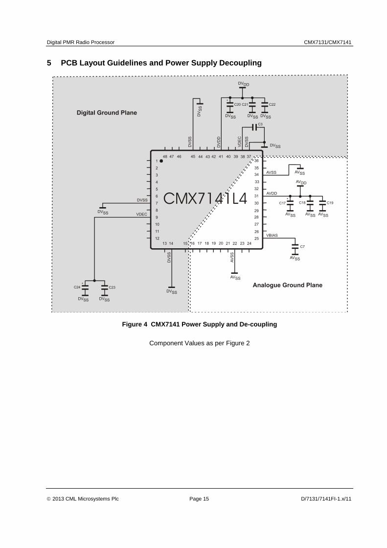
5 PCB Layout Guidelines and Power Supply Decoupling
Figure 4 CMX7141 Power Supply and De-coupling
Component Values as per Figure 2
Digital PMR Radio Processor CMX7131/CMX7141
2013 CML Microsystems Plc Page 16 D/7131/7141FI-1.x/11
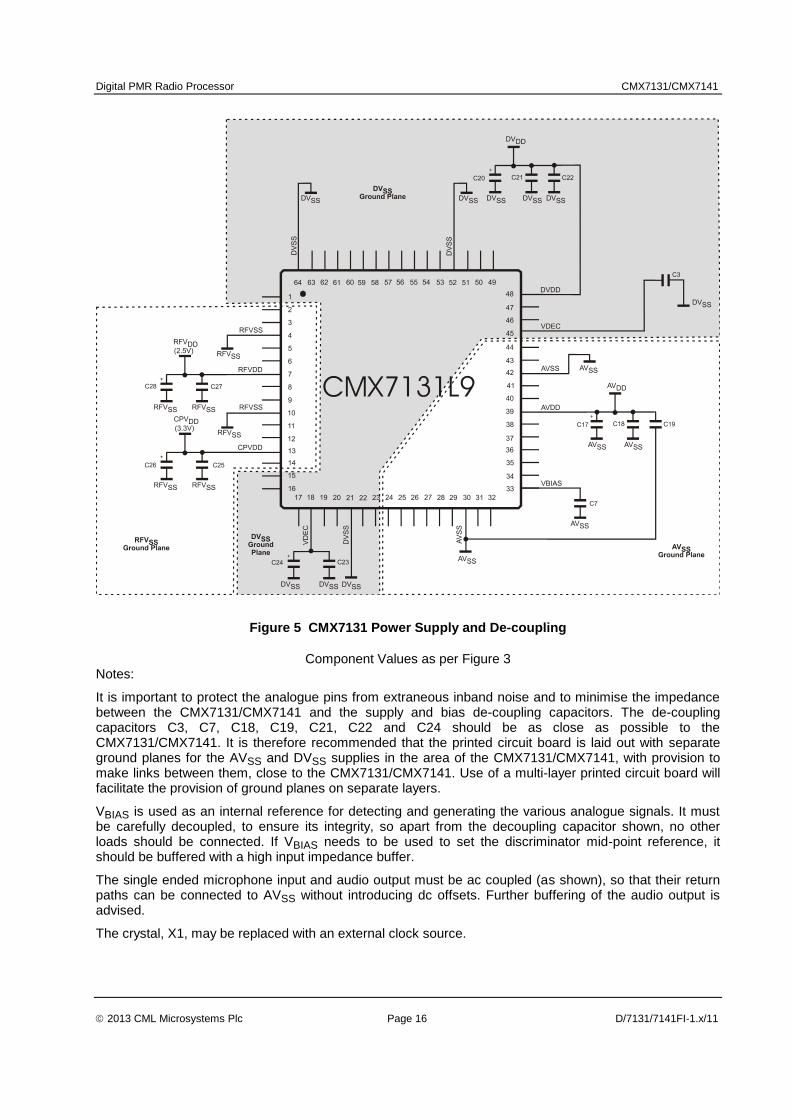
Figure 5 CMX7131 Power Supply and De-coupling
Component Values as per Figure 3 Notes:
It is important to protect the analogue pins from extraneous inband noise and to minimise the impedance between the CMX7131/CMX7141 and the supply and bias de-coupling capacitors. The de-coupling capacitors C3, C7, C18, C19, C21, C22 and C24 should be as close as possible to the CMX7131/CMX7141. It is therefore recommended that the printed circuit board is laid out with separate ground planes for the AVSS and DVSS supplies in the area of the CMX7131/CMX7141, with provision to make links between them, close to the CMX7131/CMX7141. Use of a multi-layer printed circuit board will facilitate the provision of ground planes on separate layers.
VBIAS is used as an internal reference for detecting and generating the various analogue signals. It must be carefully decoupled, to ensure its integrity, so apart from the decoupling capacitor shown, no other loads should be connected. If VBIAS needs to be used to set the discriminator mid-point reference, it should be buffered with a high input impedance buffer.
The single ended microphone input and audio output must be ac coupled (as shown), so that their return paths can be connected to AVSS without introducing dc offsets. Further buffering of the audio output is advised.
The crystal, X1, may be replaced with an external clock source.
Digital PMR Radio Processor CMX7131/CMX7141
2013 CML Microsystems Plc Page 17 D/7131/7141FI-1.x/11
6 General Description
6.1 7131/7141 FI-1.x Features The 7131/7141FI-1.x Function Image™ is intended for use in half duplex digital PMR equipment using 4FSK modulation at 4800 or 9600 bps suitable for 6.25kHz and 12.5kHz channel systems.
Much of the dPMR ETSI TS 102 490 standard Air Interface protocol is embedded in the 7131/7141FI-1.x Function Image™ operation namely:
Air Interface Physical Layer 1
4FSK modulation and demodulation
Bit and symbol definition
Frequency and symbol synchronisation
Transmission burst building and splitting
Air Interface Data Link Layer 2
Channel coding (FEC, CRC)
Interleaving, de-interleaving and bit ordering
Frame and superframe building and synchronising
Burst and parameter definition
Link addressing (source and destination)
Interfacing of voice applications (voice data) with the Physical Layer
Data bearer services
Exchanging signalling and/or user data with the Call Control Layer
Automatic Own-ID and Group-ID detection
A flexible power control facility allows the device to be placed in its optimum powersave mode when not actively processing signals.
The device includes a crystal clock generator, with buffered output, to provide a common system clock if required.
A block diagram of the device is shown in Figure 1.
The signal processing blocks can be routed from any of the three DISC/ALT/MIC input pins.
Other Functions Include:
Automatic Tx Sequencer simplifies host control
RAMDAC operation
TXENA and RXENA hardware signals
Two-point or I/Q modulation outputs
Hard or soft data output options
Auxiliary Functions:
Two programmable system clock outputs
Two auxiliary ADCs with four selectable external input paths
Four auxiliary DACs, one with built-in programmable RAMDAC
Two RF PLLs (CMX7131 only)
Digital PMR Radio Processor CMX7131/CMX7141
2013 CML Microsystems Plc Page 18 D/7131/7141FI-1.x/11
Interface:
Optimised C-BUS (4 wire high speed synchronous serial command/data bus) interface to host for control and data transfer
Open drain IRQ to host
Auxiliary SPI/C-BUS interface to CMX618/CMX608 with pass-through mode from host
SPI bus interface for speech codec to support third-party vocoders
Two GPIO pins
Serial memory boot mode
C-BUS (host) boot mode
6.2 System Design A number of system architectures can be supported by the device. The most highly integrated solution uses a CMX618 Vocoder under full control of the CMX7131/CMX7141, relieving the host of all vocoder management duties. In this mode audio codec functions are provided by the CMX618. Other architectures using third-party vocoders are supported using SPI-Codec mode in which the CMX7131/CMX7141 acts as an external audio codec attached to the vocoder. In this mode the host must issue all control commands to the vocoder, and also transfer coded data packets between the vocoder and CMX7131/CMX7141.
The configuration of the Auxiliary SPI/C-BUS port is controlled by the SPI-Codec enable bit ($B1 bit 0).
SPI-Codec $B1:0
Port Mode
0 C-BUS Connect to CMX6x8 C-BUS port (default)
1 SPI Connect to CMX608 or third-party vocoder SPI codec port
In SPI-Codec mode 16-bit PCM audio samples are transferred at 8ksps. When this mode is selected:
in Tx: the CMX7131/CMX7141 microphone input should be routed from MIC to Input2. The input signal is lowpass filtered, converted to 16-bit linear PCM at 8ksps and then output on the EPSI pin of the SPI-Codec port for the external vocoder to process.
in Rx: the CMX7131/CMX7141 audio output should be routed to Output1. 16-bit linear PCM samples are read from the EPSO pin of the SPI-Codec port, then filtered and output via the Audio Output Attenuator.
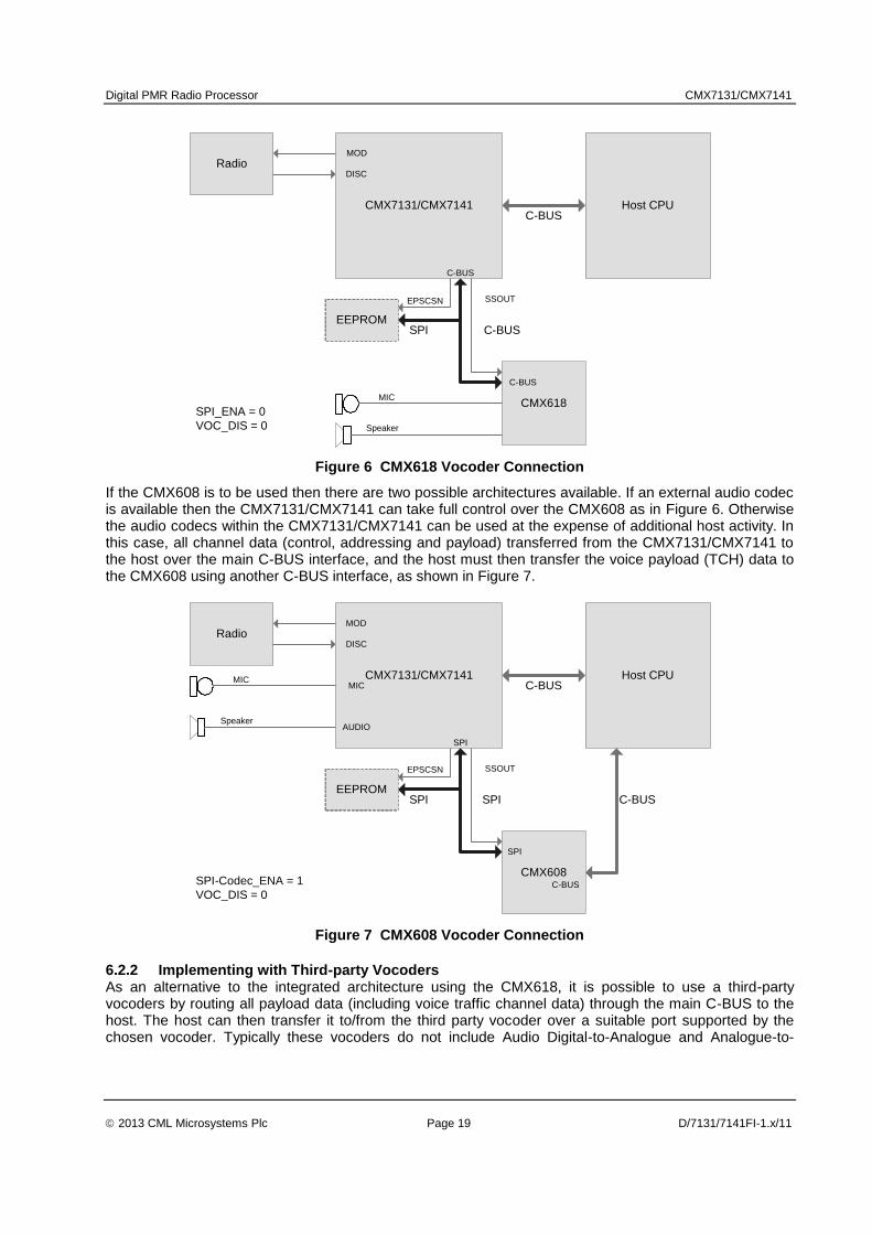
6.2.1 Implementation using the CMX6x8 Figure 6 shows the configuration using the CMX618 RALCWI Vocoder where all control and data is handled by the CMX7131/CMX7141 with minimal host CPU involvement:
Digital PMR Radio Processor CMX7131/CMX7141
2013 CML Microsystems Plc Page 19 D/7131/7141FI-1.x/11
CMX7131/CMX7141 Host CPU
CMX618
Radio
EEPROM
C-BUS
DISC
MOD
SPI
EPSCSN SSOUT
SPI_ENA = 0
VOC_DIS = 0
C-BUS
C-BUS
C-BUS
MIC
Speaker
Figure 6 CMX618 Vocoder Connection
If the CMX608 is to be used then there are two possible architectures available. If an external audio codec is available then the CMX7131/CMX7141 can take full control over the CMX608 as in Figure 6. Otherwise the audio codecs within the CMX7131/CMX7141 can be used at the expense of additional host activity. In this case, all channel data (control, addressing and payload) transferred from the CMX7131/CMX7141 to the host over the main C-BUS interface, and the host must then transfer the voice payload (TCH) data to the CMX608 using another C-BUS interface, as shown in Figure 7.
CMX7131/CMX7141 Host CPU
CMX608
Radio
EEPROM
C-BUS
DISC
MOD
SPI
EPSCSN SSOUT
SPI-Codec_ENA = 1
VOC_DIS = 0
SPI
SPI
SPI
MIC
Speaker
C-BUS
C-BUS
MIC
AUDIO
Figure 7 CMX608 Vocoder Connection
6.2.2 Implementing with Third-party Vocoders As an alternative to the integrated architecture using the CMX618, it is possible to use a third-party vocoders by routing all payload data (including voice traffic channel data) through the main C-BUS to the host. The host can then transfer it to/from the third party vocoder over a suitable port supported by the chosen vocoder. Typically these vocoders do not include Audio Digital-to-Analogue and Analogue-to-

Digital PMR Radio Processor CMX7131/CMX7141
2013 CML Microsystems Plc Page 20 D/7131/7141FI-1.x/11
Digital converters, so the CMX7131/CMX7141 can be configured to use its auxiliary C-BUS as an SPI interface and use its built-in DAC/ADCs as audio converters. This architecture is shown in Figure 8.
CMX7131/CMX7141 Host CPU
DVSI
Vocoder
Radio
EEPROM
C-BUS
DISC
MOD
SPI
EPSCSN SSOUT
SPI-Codec_ENA = 1
VOC_DIS = 0
SPI
SPI
SPI
MIC
Speaker
Serial
UART
MIC
AUDIO
Figure 8 DVSI Vocoder Connection
Additionally, this architecture can be extended to support a dual-mode system with two different vocoders, though this requires some additional host switching as shown in Figure 9. The Vocoder Enable Masks in Program Block 1 should be set up by the host following power-on, to allow the CMX7131/CMX7141 to configure the SPI interface correctly for each call depending on which vocoder is required.
CMX7131/CMX7141 Host CPU
DVSI
Vocoder
Radio
EEPROM
C-BUS
DISC
MOD
SPI
EPSCSN SSOUT
SPI-Codec_ENA = 1
VOC_DIS = 0
SPI
SPI
SPI
MIC
Speaker
Serial
UART
MIC
AUDIO
CMX608C-BUS
C-BUS
mux
SPI
Figure 9 Dual Vocoder Connection
Digital PMR Radio Processor CMX7131/CMX7141
2013 CML Microsystems Plc Page 21 D/7131/7141FI-1.x/11
6.2.3 Data Transfer When transmitting, an initial block of payload or control channel data will need to be loaded from the host into the C-BUS TxData registers. The CMX7131/CMX7141 can then format and transmit that data while at the same time loading in the following data blocks from the host or CMX618.
When receiving, the host needs to consider that when a signal is received over the air there will be a processing delay while the CMX7131/CMX7141 filters, demodulates and decodes the output data before presenting it to the host or CMX618. For best performance voice payload data can be output in soft-decision (4-bit log-likelihood ratio) format compatible with the CMX618/CMX608 and other third-party vocoders, although this mode increases the data transfer rate over C-BUS by a factor of four.
6.2.4 RSSI Measurement The AuxADC provided by the CMX7131/CMX7141 can be used to detect the Squelch or RSSI signal from the RF section while the device is in Rx or Idle mode. This allows a significant degree of powersaving within the CMX7131/CMX7141 and avoids the need to wake the host up unnecessarily. The host programmable AuxADC thresholds allow for user selection of squelch threshold settings.
6.2.5 Serial Memory Connection In all cases, the auxiliary C-BUS/SPI-Codec bus is shared with the serial memory bus, which may be used to load the contents of the Function Image™. Bus conflicts are avoided by the use of an additional Chip Select signal (SSOUT). If this feature is not used then the EPSCSN pin should be left un-connected.
6.3 Introduction This modem can run at either 4800bps or 9600bps, occupying a 6.25kHz or a 12.5kHz bandwidth RF channel respectively. It has been designed such that, when combined with suitable RF, host controller, CMX618/CMX608 Vocoder and appropriate control software, it meets the requirements of the EN 301 166 or EN 300 113 standards as appropriate. See www.etsi.org for details of these standards.
TS 102 490 is available on the ETSI web site (www.etsi.org) which describes a 6.25kHz channel spacing FDMA dPMR system. This standard uses a 4FSK modulation scheme with an over-air bit rate of 4800bps (ie. 2400 symbols per second). With respect to dPMR formatted modes of operation, this document should be read in conjunction with the ETSI standard.
The dPMR standard does not specify a voice coding algorithm, but the CMX618 or CMX608 (also available from CML) are both suitable devices for this purpose. In the rest of this document these two devices are referred to generically as the CMX6x8, as the only significant difference between them is the inclusion of an on-chip audio codec in the CMX618 while the CMX608 requires an external Audio Codec.
Version 1.5.1 of TS 102 490 introduces two additional vocoder control bits which specify which vocoder is in use for a particular voice call. Function Image 1.1.0.0 onwards supports these additional bits, however care should be taken if backwards compatibility with earlier implementations is to be maintained.
Note that the TS 102 490 (dPMR) standard is NOT compatible with the TS 102 361 (DMR)
12.5kHz/9600baud TDMA system.
The 9600bps option is made available for customer-specific applications only – this mode does not support automated control of the CMX6x8 – in which case all data should be routed via the host.
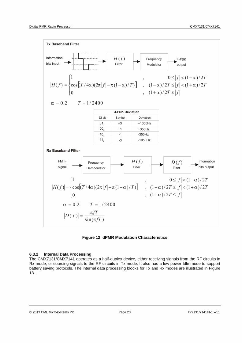
6.3.1 Modulation The dPMR 4FSK modulation scheme operates in a 6.25kHz channel bandwidth with a deviation index of 0.29 and has an over-air bit rate of 4800bps (2400 symbols per second). RRC filters are implemented in both Tx and Rx with a filter “alpha” of 0.2. The maximum frequency error is +/-625Hz and the CMX7131/CMX7141 can adapt to the maximum time-base clock drift of 2ppm over the duration of a 180-second burst. Figure 12 shows the basic parameters of the 4FSK modulation, symbol mapping and filtering requirements.
The 9600bps mode provided by the CMX7131/CMX7141 is essentially the same as the 4800bps mode, but with all timings modified by a factor of two.
Digital PMR Radio Processor CMX7131/CMX7141
2013 CML Microsystems Plc Page 22 D/7131/7141FI-1.x/11
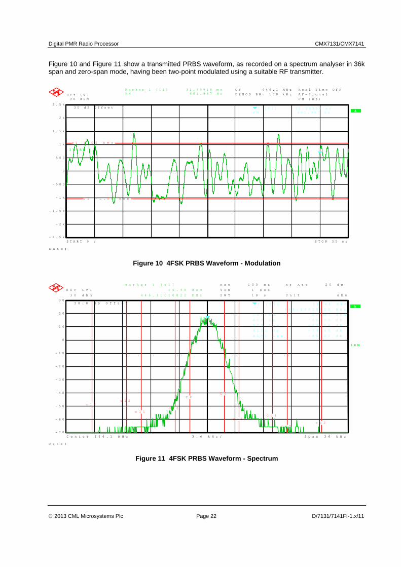
Figure 10 and Figure 11 show a transmitted PRBS waveform, as recorded on a spectrum analyser in 36k span and zero-span mode, having been two-point modulated using a suitable RF transmitter.
R e f
L v l
3 0
d B m
3 0
d B m
R e f L v l
3 0
d B m
3 0
d B m
3 0
d B
O f f s e t
A
S T A R T 0 s S T O P
3 5
m s
C F 4 4 6 . 1 M H z
D E M O D B W :
1 0 0
k H z
R e a l T i m e
O F F
A F - S i g n a l F M
[ H z ]
5 0 0
1 V I E W
- 2 k
- 1 . 5 k
- 1 k - 5 0 0
0
5 0 0
1 k
1 . 5 k
2 k
- 2 . 5 k
2 . 5 k
1
M a r k e r 1 [ T 1 ]
3 1 . 3 9 9 1 8
m s
F M
6 6 1 . 9 8 7 H z
1 [ T 1 ]
3 1 . 3 9 9 1 8
m s
F M
6 6 1 . 9 8 7 H z
D 1 1 . 0 5
k H z
D 2 - 1 . 0 5
k H z
D a t e :
Figure 10 4FSK PRBS Waveform - Modulation
A
R B W 1 0 0
H z
V B W 1 k H z
S W T 1 8
s U n i t d B m
1 R M
3 0 . 8
d B
O f f s e t
R e f L v l
3 0
d B m
R e f L v l
3 0
d B m
R F A t t
2 0
d B
3 . 6 k H z / C e n t e r 4 4 6 . 1
M H z S p a n 3 6
k H z
- 6 0
- 5 0
- 4 0
- 3 0
- 2 0
- 1 0
0
1 0
2 0
- 7 0
3 0
1
M a r k e r 1 [ T 1 ]
1 6 . 4 8 d B m
4 4 6 . 1 0 0 1 0 8 2 2
M H z
1 [ T 1 ]
1 6 . 4 8
d B m
4 4 6 . 1 0 0 1 0 8 2 2
M H z
C H P W R
2 7 . 5 3
d B m
A C P U p
- 6 6 . 5 5
d B
A C P L o w
- 6 7 . 1 4
d B
A L T 1 U p
- 7 9 . 4 5
d B
A L T 1 L o w
- 8 0 . 2 1
d B
c u 2 c u 2 c u 1 c u 1 c l 1
c l 1 c l 2 c l 2 C 0 C 0
D a t e :
Figure 11 4FSK PRBS Waveform - Spectrum
Digital PMR Radio Processor CMX7131/CMX7141
2013 CML Microsystems Plc Page 23 D/7131/7141FI-1.x/11
Figure 12 dPMR Modulation Characteristics
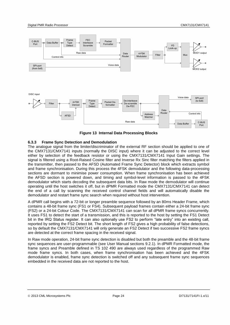
6.3.2 Internal Data Processing The CMX7131/CMX7141 operates as a half-duplex device, either receiving signals from the RF circuits in Rx mode, or sourcing signals to the RF circuits in Tx mode. It also has a low power Idle mode to support battery saving protocols. The internal data processing blocks for Tx and Rx modes are illustrated in Figure 13.
Digital PMR Radio Processor CMX7131/CMX7141
2013 CML Microsystems Plc Page 24 D/7131/7141FI-1.x/11
C-BUS
PortData Buffer
Frame
Type
Detect
FEC
Interleave
Scramble
Packet
Formatter
Data
Router
SPI-port
(from 6x8)
4-FSK
ModulatorFilter
I/Q
Look-up
Mux
Filter
AFSD
4-FSK
Demod
Frame
Type
Detect
De-interleave
De-scramble
De-FEC
Data
Router
SPI-port
(to 6x8)
Data Buffer
Address
Matcher
C-BUS
Port
Packet De-
formatter
DISC input
MOD1 output
MOD2 output
Raw data
Raw data
Control info
Control info
Voice data
Voice data
Figure 13 Internal Data Processing Blocks
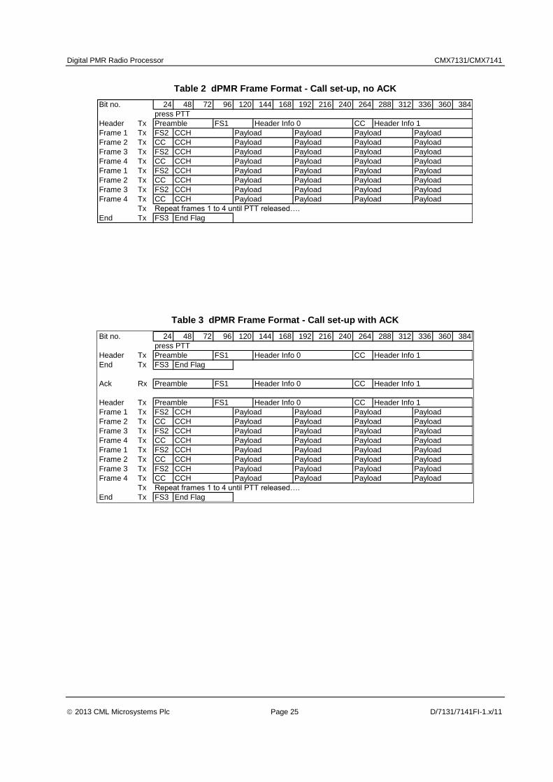
6.3.3 Frame Sync Detection and Demodulation The analogue signal from the limiter/discriminator of the external RF section should be applied to one of the CMX7131/CMX7141 inputs (normally the DISC input) where it can be adjusted to the correct level either by selection of the feedback resistor or using the CMX7131/CMX7141 Input Gain settings. The signal is filtered using a Root-Raised Cosine filter and Inverse Rx Sinc filter matching the filters applied in the transmitter, then passed to the AFSD (Automated Frame Sync Detector) block which extracts symbol and frame synchronisation. During this process the 4FSK demodulator and the following data-processing sections are dormant to minimise power consumption. When frame synchronisation has been achieved the AFSD section is powered down, and timing and symbol-level information is passed to the 4FSK demodulator which starts decoding the subsequent data bits. In Raw mode the demodulator will continue operating until the host switches it off, but in dPMR Formatted mode the CMX7131/CMX7141 can detect the end of a call by scanning the received control channel fields and will automatically disable the demodulator and restart frame sync search when required without host intervention.
A dPMR call begins with a 72-bit or longer preamble sequence followed by an 80ms Header Frame, which contains a 48-bit frame sync (FS1 or FS4). Subsequent payload frames contain either a 24-bit frame sync (FS2) or a 24-bit Colour Code. The CMX7131/CMX7141 can scan for all dPMR frame syncs concurrently. It uses FS1 to detect the start of a transmission, and this is reported to the host by setting the FS1 Detect bit in the IRQ Status register. It can also optionally use FS2 to perform “late entry” into an existing call, reported by setting the FS2 Detect bit. The short length of FS2 gives a high probability of false detections, so by default the CMX7131/CMX7141 will only generate an FS2 Detect if two successive FS2 frame syncs are detected at the correct frame spacing in the received signal.
In Raw mode operation, 24-bit frame sync detection is disabled but both the preamble and the 48-bit frame sync sequences are user-programmable (see User Manual sections 9.2.1). In dPMR Formatted mode, the frame syncs and Preamble defined in TS 102 490 are always used regardless of the programmed Raw mode frame syncs. In both cases, when frame synchronisation has been achieved and the 4FSK demodulator is enabled, frame sync detection is switched off and any subsequent frame sync sequences embedded in the received data are not reported to the host.
Digital PMR Radio Processor CMX7131/CMX7141
2013 CML Microsystems Plc Page 25 D/7131/7141FI-1.x/11
Table 2 dPMR Frame Format - Call set-up, no ACK
Bit no. 24 48 72 96 120 144 168 192 216 240 264 288 312 336 360 384
press PTT
Header Tx CC
Frame 1 Tx FS2 CCH Payload Payload Payload Payload
Frame 2 Tx CC CCH Payload Payload Payload Payload
Frame 3 Tx FS2 CCH Payload Payload Payload Payload
Frame 4 Tx CC CCH Payload Payload Payload Payload
Frame 1 Tx FS2 CCH Payload Payload Payload Payload
Frame 2 Tx CC CCH Payload Payload Payload Payload
Frame 3 Tx FS2 CCH Payload Payload Payload Payload
Frame 4 Tx CC CCH Payload Payload Payload Payload
Tx Repeat frames 1 to 4 until PTT released….
End Tx FS3
Header Info 1Header Info 0
End Flag
Preamble FS1
Table 3 dPMR Frame Format - Call set-up with ACK
Bit no. 24 48 72 96 120 144 168 192 216 240 264 288 312 336 360 384
press PTT
Header Tx CC
End Tx FS3
Ack Rx CC
Header Tx CC
Frame 1 Tx FS2 CCH Payload Payload Payload Payload
Frame 2 Tx CC CCH Payload Payload Payload Payload
Frame 3 Tx FS2 CCH Payload Payload Payload Payload
Frame 4 Tx CC CCH Payload Payload Payload Payload
Frame 1 Tx FS2 CCH Payload Payload Payload Payload
Frame 2 Tx CC CCH Payload Payload Payload Payload
Frame 3 Tx FS2 CCH Payload Payload Payload Payload
Frame 4 Tx CC CCH Payload Payload Payload Payload
Tx Repeat frames 1 to 4 until PTT released….
End Tx FS3
Header Info 1Header Info 0
End Flag
Preamble FS1 Header Info 0
Preamble FS1
Header Info 1
End Flag
Preamble FS1 Header Info 0 Header Info 1

Digital PMR Radio Processor CMX7131/CMX7141
2013 CML Microsystems Plc Page 26 D/7131/7141FI-1.x/11
Rx enabled
AFSD active
4FSK dormant
FS1 detected?
AFSD off
4FSK active
IRQ FS1
FS2 detected?
AFSD off
4FSK active
IRQ FS2
Demodulate Demodulate
IRQ FS2
CC detected?
FS2 detected?
ID & CC
matched?
IRQ Called
IRQ DataRDY
(HDR + LE)
Enable 6x8
Transfer data to
6x8
END detected?
IRQ DataRDY
(END)
no
no
no
no
no no
ID & CC
matched?
no
Process data
AFSD process
Analyse CCH data
decode,
de-interleave
Analyse HDR data
decode,
de-interleave
IRQ Called
IRQ DataRDY
(HDR)
Disable 6x8
Figure 14 FS Detection
Digital PMR Radio Processor CMX7131/CMX7141
2013 CML Microsystems Plc Page 27 D/7131/7141FI-1.x/11
6.3.4 FEC and Coding In Raw mode the CMX7131/CMX7141 does not implement any FEC processing.
In dPMR Formatted mode the CMX7131/CMX7141 implements all CRCs, Hamming codes, interleaving and scrambling required by the dPMR standard. CRC failures in control channel fields and coded data blocks are indicated to the host by issuing an “Event” IRQ with a corresponding error code in the Modem Status register, $C9. This relieves the host of a substantial processing load and has the added advantage of reducing the complexity and timing constraints of interfacing between the host, vocoder and CMX7131/CMX7141.
The dPMR Header Frame format contains duplicate copies of all control channel fields (in the HI0 and HI1 Header Information blocks) but only one decoded copy of each field will be presented back to the host. On receiving a Header Frame the CMX7131/CMX7141 decodes both HI blocks, checks CRCs and can accept the call if either block is valid (the other HI block is discarded).
6.3.5 Voice Coding A CML CMX618 or CMX608 RALCWI vocoder can be used under the control of the CMX7131/CMX7141. The CMX7131/CMX7141 provides an auxiliary SPI/C-BUS port (shared with the boot serial memory) which is used to issue control commands and transfer voice payload data directly to the CMX6x8 vocoder, minimising the loading on the host controller during voice calls.
Alternatively, the CMX7131/CMX7141 can support any third-party vocoder by routing voice payload data over the main C-BUS interface and through the host. In this mode, all vocoder control and data transfers must be managed by the host.
Voice data transferred to the CMX6x8 in Rx mode always uses soft decision (4-bit log-likelihood ratio) format. This option is also available for voice payload data routed to the host, although it increases the required data transfer rate over C-BUS by a factor of four.
6.3.6 Radio Performance Requirements The CMX7131/CMX7141 demodulator is designed to process a 4FSK signal from a limiter/discriminator source. For optimum performance the signal should not be significantly degraded by filters that are excessively narrow and/or cause significant group delay distortion. Care should be taken in interfacing the device to the radio circuits to maintain the frequency and phase response (both low and high end), in order to achieve optimum performance. Test modes are provided to assist in both the initial design and production set-up procedures.
Further information and application notes can be found at http://www.cmlmicro.com .
Digital PMR Radio Processor CMX7131/CMX7141
2013 CML Microsystems Plc Page 28 D/7131/7141FI-1.x/11
7 Detailed Descriptions
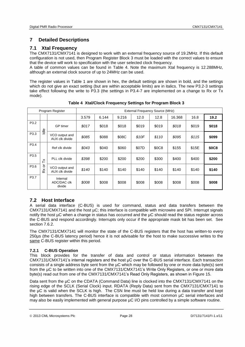
7.1 Xtal Frequency The CMX7131/CMX7141 is designed to work with an external frequency source of 19.2MHz. If this default configuration is not used, then Program Register Block 3 must be loaded with the correct values to ensure that the device will work to specification with the user selected clock frequency. A table of common values can be found in Table 4. Note the maximum Xtal frequency is 12.288MHz, although an external clock source of up to 24MHz can be used. The register values in Table 1 are shown in hex, the default settings are shown in bold, and the settings which do not give an exact setting (but are within acceptable limits) are in italics. The new P3.2-3 settings take effect following the write to P3.3 (the settings in P3.4-7 are implemented on a change to Rx or Tx mode).
Table 4 Xtal/Clock Frequency Settings for Program Block 3
Program Register External Frequency Source (MHz)
3.579 6.144 9.216 12.0 12.8 16.368 16.8 19.2
P3.2
Idle
GP timer $017 $018 $018 $019 $019 $018 $019 $018
P3.3 VCO output and AUX clk divide
$085 $088 $08C $10F $110 $095 $115 $099
P3.4
Rx o
r T
x
Ref clk divide $043 $040 $060 $07D $0C8 $155 $15E $0C8
P3.5 PLL clk divide $398 $200 $200 $200 $300 $400 $400 $200
P3.6 VCO output and AUX clk divide
$140 $140 $140 $140 $140 $140 $140 $140
P3.7 Internal ADC/DAC clk
divide $008 $008 $008 $008 $008 $008 $008 $008
7.2 Host Interface A serial data interface (C-BUS) is used for command, status and data transfers between the CMX7131/CMX7141 and the host µC; this interface is compatible with microwire and SPI. Interrupt signals notify the host µC when a change in status has occurred and the µC should read the status register across the C-BUS and respond accordingly. Interrupts only occur if the appropriate mask bit has been set. See section 7.6.2.
The CMX7131/CMX7141 will monitor the state of the C-BUS registers that the host has written-to every 250µs (the C-BUS latency period) hence it is not advisable for the host to make successive writes to the same C-BUS register within this period.
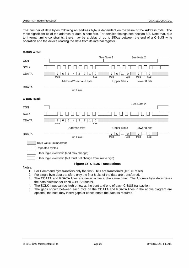
7.2.1 C-BUS Operation This block provides for the transfer of data and control or status information between the CMX7131/CMX7141’s internal registers and the host µC over the C-BUS serial interface. Each transaction consists of a single address byte sent from the µC which may be followed by one or more data byte(s) sent from the µC to be written into one of the CMX7131/CMX7141’s Write Only Registers, or one or more data byte(s) read out from one of the CMX7131/CMX7141’s Read Only Registers, as shown in Figure 15.
Data sent from the µC on the CDATA (Command Data) line is clocked into the CMX7131/CMX7141 on the rising edge of the SCLK (Serial Clock) input. RDATA (Reply Data) sent from the CMX7131/CMX7141 to the µC is valid when the SCLK is high. The CSN line must be held low during a data transfer and kept high between transfers. The C-BUS interface is compatible with most common µC serial interfaces and may also be easily implemented with general purpose µC I/O pins controlled by a simple software routine.
Digital PMR Radio Processor CMX7131/CMX7141
2013 CML Microsystems Plc Page 29 D/7131/7141FI-1.x/11
The number of data bytes following an address byte is dependent on the value of the Address byte. The most significant bit of the address or data is sent first. For detailed timings see section 8.2. Note that, due to internal timing constraints, there may be a delay of up to 250µs between the end of a C-BUS write operation and the device reading the data from its internal register.
C-BUS Write:
See Note 1 See Note 2
CSN
SCLK
CDATA 7 6 5 4 3 2 1 0 7 6 … 0 7 … 0 MSB LSB MSB LSB MSB LSB
Address/Command byte Upper 8 bits Lower 8 bits
RDATA
High Z state
C-BUS Read:
See Note 2
CSN
SCLK
CDATA 7 6 5 4 3 2 1 0 MSB LSB
Address byte Upper 8 bits Lower 8 bits
RDATA
7 6 … 0 7 … 0
High Z state MSB LSB MSB LSB
Data value unimportant
Repeated cycles
Either logic level valid (and may change)
Either logic level valid (but must not change from low to high)
Figure 15 C-BUS Transactions Notes:
1. For Command byte transfers only the first 8 bits are transferred ($01 = Reset). 2. For single byte data transfers only the first 8 bits of the data are transferred. 3. The CDATA and RDATA lines are never active at the same time. The Address byte determines
the data direction for each C-BUS transfer. 4. The SCLK input can be high or low at the start and end of each C-BUS transaction. 5. The gaps shown between each byte on the CDATA and RDATA lines in the above diagram are
optional, the host may insert gaps or concatenate the data as required.
Digital PMR Radio Processor CMX7131/CMX7141
2013 CML Microsystems Plc Page 30 D/7131/7141FI-1.x/11
7.3 Function Image™ Loading The Function Image™ (FI), which defines the operational capabilities of the device, may be obtained from the CML Technical Portal, following registration. This is in the form of a 'C' header file which can be included into the host controller software or programmed into an external serial memory. The maximum possible size of Function Image
TM is 46 kbytes, although a typical FI will be less than this. Note that the
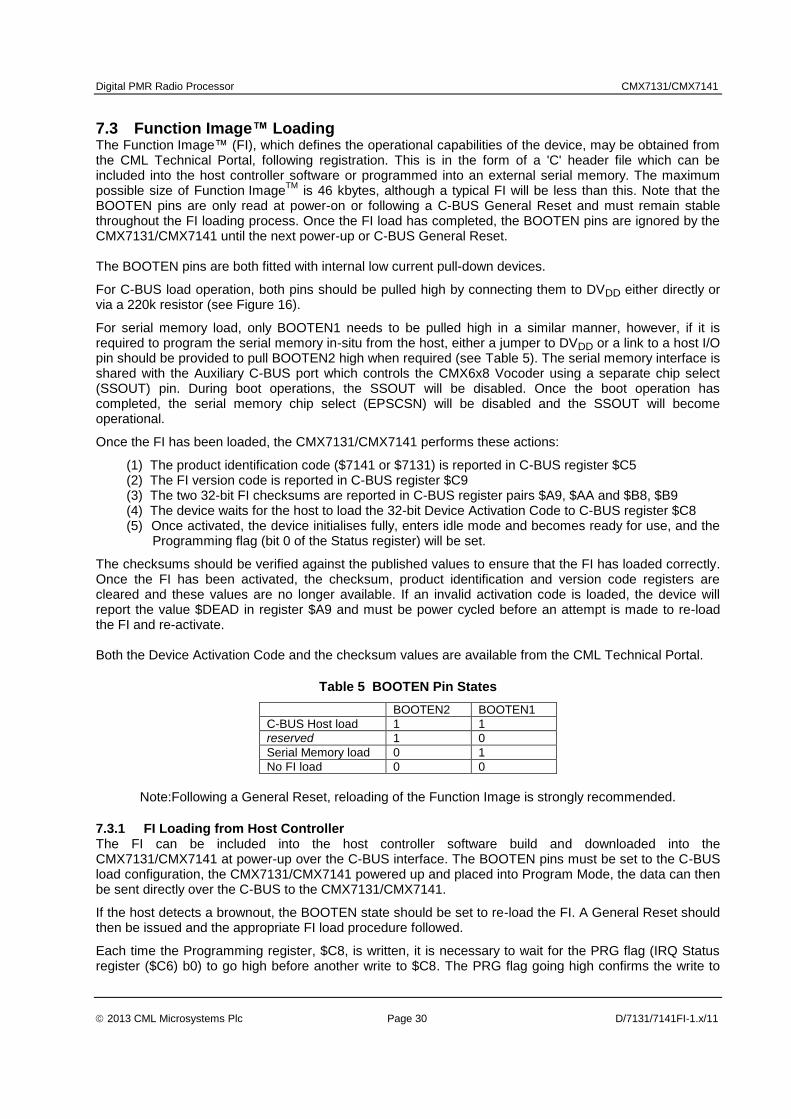
BOOTEN pins are only read at power-on or following a C-BUS General Reset and must remain stable throughout the FI loading process. Once the FI load has completed, the BOOTEN pins are ignored by the CMX7131/CMX7141 until the next power-up or C-BUS General Reset. The BOOTEN pins are both fitted with internal low current pull-down devices.
For C-BUS load operation, both pins should be pulled high by connecting them to DVDD either directly or via a 220k resistor (see Figure 16).
For serial memory load, only BOOTEN1 needs to be pulled high in a similar manner, however, if it is required to program the serial memory in-situ from the host, either a jumper to DVDD or a link to a host I/O pin should be provided to pull BOOTEN2 high when required (see Table 5). The serial memory interface is shared with the Auxiliary C-BUS port which controls the CMX6x8 Vocoder using a separate chip select (SSOUT) pin. During boot operations, the SSOUT will be disabled. Once the boot operation has completed, the serial memory chip select (EPSCSN) will be disabled and the SSOUT will become operational.
Once the FI has been loaded, the CMX7131/CMX7141 performs these actions:
(1) The product identification code ($7141 or $7131) is reported in C-BUS register $C5 (2) The FI version code is reported in C-BUS register $C9 (3) The two 32-bit FI checksums are reported in C-BUS register pairs $A9, $AA and $B8, $B9 (4) The device waits for the host to load the 32-bit Device Activation Code to C-BUS register $C8 (5) Once activated, the device initialises fully, enters idle mode and becomes ready for use, and the
Programming flag (bit 0 of the Status register) will be set.
The checksums should be verified against the published values to ensure that the FI has loaded correctly. Once the FI has been activated, the checksum, product identification and version code registers are cleared and these values are no longer available. If an invalid activation code is loaded, the device will report the value $DEAD in register $A9 and must be power cycled before an attempt is made to re-load the FI and re-activate. Both the Device Activation Code and the checksum values are available from the CML Technical Portal.
Table 5 BOOTEN Pin States
BOOTEN2 BOOTEN1
C-BUS Host load 1 1
reserved 1 0
Serial Memory load 0 1
No FI load 0 0
Note:Following a General Reset, reloading of the Function Image is strongly recommended.
7.3.1 FI Loading from Host Controller The FI can be included into the host controller software build and downloaded into the CMX7131/CMX7141 at power-up over the C-BUS interface. The BOOTEN pins must be set to the C-BUS load configuration, the CMX7131/CMX7141 powered up and placed into Program Mode, the data can then be sent directly over the C-BUS to the CMX7131/CMX7141.
If the host detects a brownout, the BOOTEN state should be set to re-load the FI. A General Reset should then be issued and the appropriate FI load procedure followed.
Each time the Programming register, $C8, is written, it is necessary to wait for the PRG flag (IRQ Status register ($C6) b0) to go high before another write to $C8. The PRG flag going high confirms the write to

Digital PMR Radio Processor CMX7131/CMX7141
2013 CML Microsystems Plc Page 31 D/7131/7141FI-1.x/11
the Programming register has been accepted. The PRG flag state can be determined by polling the IRQ Status register or by unmasking the interrupt (Interrupt Mask register, $CE, b0).
The download time is limited by the clock frequency of the C-BUS, with a 5MHz SCLK, it should take less than 500ms to complete (host dependent).
BOOTEN 2 = 1
BOOTEN 1 = 1
Power-up or
write General Reset to device
Poll $C6 until b0 = 1 (Programming mode entered)
Configure PRG flag interrupt if required
Write $0001 to $C8
Write Start Block 1 Address (DB1_ptr) to $B6
Write Block 1 Length (DB1_len) to $B7
Wait for PRG flag to go high or interrupt
Write next data word to $C8
Wait for PRG flag to go high or interrupt
Write Start Block 2 Address (DB2_ptr) to $B6
Write Block 2 Length (DB2_len) to $B7
Write $0001 to $C8
Wait for PRG flag to go high or interrupt
Wait for PRG flag to go high or interrupt
Write next data word to $C8
Write Start Block 3 Address (ACTIVATE_ptr) to $B6
Write Block 3 Length (ACTIVATE_len) to $B7
Write $0001 to $C8
Wait for PRG flag to go high or interrupt
Send Activation Code hi to $C8
Read and verify checksum values in register pair :
$A9 and $AA, $B8 and $B9
Send Activation Code lo to $C8
Wait for PRG flag to go high or interrupt
Wait for PRG flag to go high or interrupt
BOOTEN1 and BOOTEN2 may be
changed from this point on, if required
Device is now ready for use
BOOTEN1
BOOTEN2
VDD
Figure 16 FI Loading from Host
Digital PMR Radio Processor CMX7131/CMX7141
2013 CML Microsystems Plc Page 32 D/7131/7141FI-1.x/11
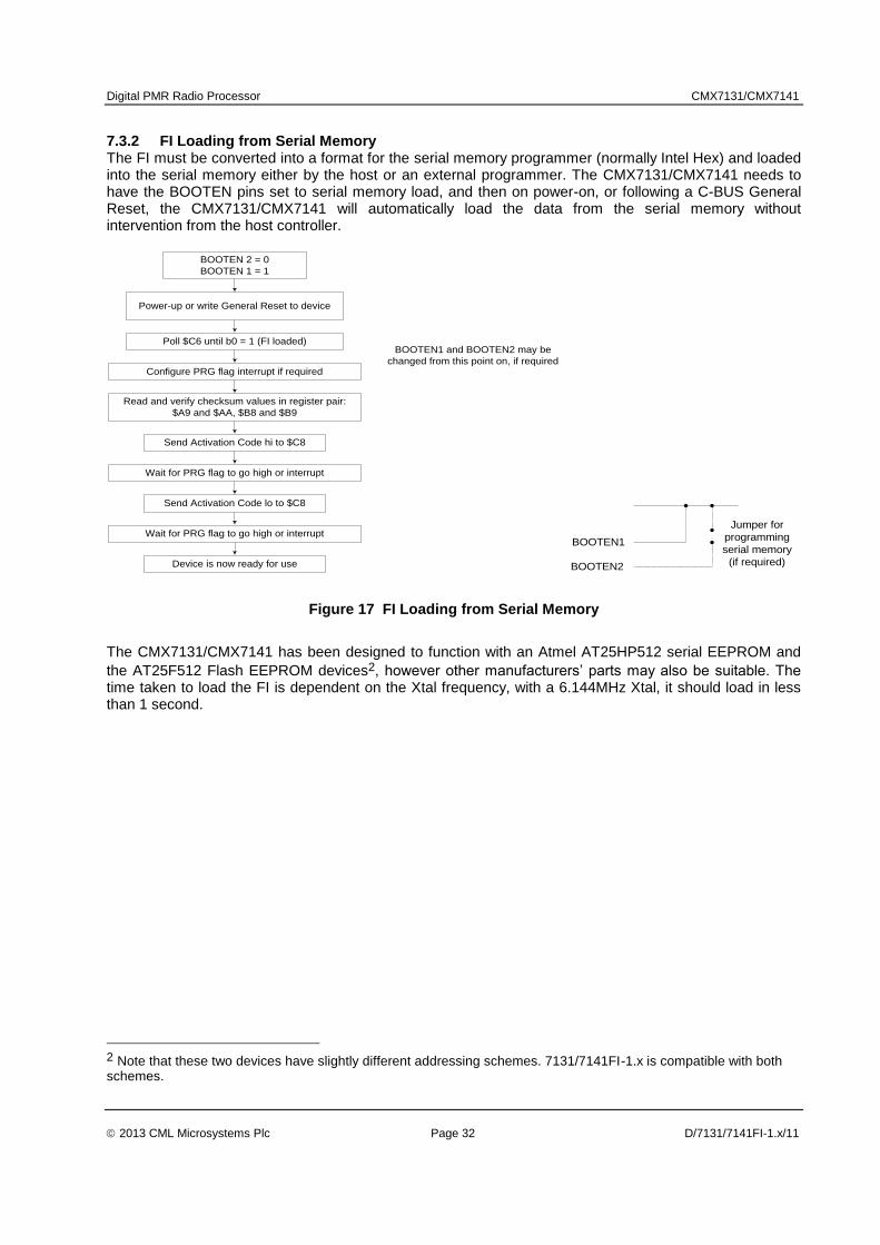
7.3.2 FI Loading from Serial Memory The FI must be converted into a format for the serial memory programmer (normally Intel Hex) and loaded into the serial memory either by the host or an external programmer. The CMX7131/CMX7141 needs to have the BOOTEN pins set to serial memory load, and then on power-on, or following a C-BUS General Reset, the CMX7131/CMX7141 will automatically load the data from the serial memory without intervention from the host controller.
BOOTEN 2 = 0
BOOTEN 1 = 1
Power-up or write General Reset to device
Poll $C6 until b0 = 1 (FI loaded)
Configure PRG flag interrupt if required
Send Activation Code hi to $C8
Read and verify checksum values in register pair:
$A9 and $AA, $B8 and $B9
Send Activation Code lo to $C8
Wait for PRG flag to go high or interrupt
Wait for PRG flag to go high or interrupt
BOOTEN1 and BOOTEN2 may be
changed from this point on, if required
Device is now ready for use
BOOTEN1
BOOTEN2
Jumper for
programming
serial memory
(if required)
Figure 17 FI Loading from Serial Memory
The CMX7131/CMX7141 has been designed to function with an Atmel AT25HP512 serial EEPROM and
the AT25F512 Flash EEPROM devices2, however other manufacturers’ parts may also be suitable. The time taken to load the FI is dependent on the Xtal frequency, with a 6.144MHz Xtal, it should load in less than 1 second. 2 Note that these two devices have slightly different addressing schemes. 7131/7141FI-1.x is compatible with both schemes.
Digital PMR Radio Processor CMX7131/CMX7141
2013 CML Microsystems Plc Page 33 D/7131/7141FI-1.x/11
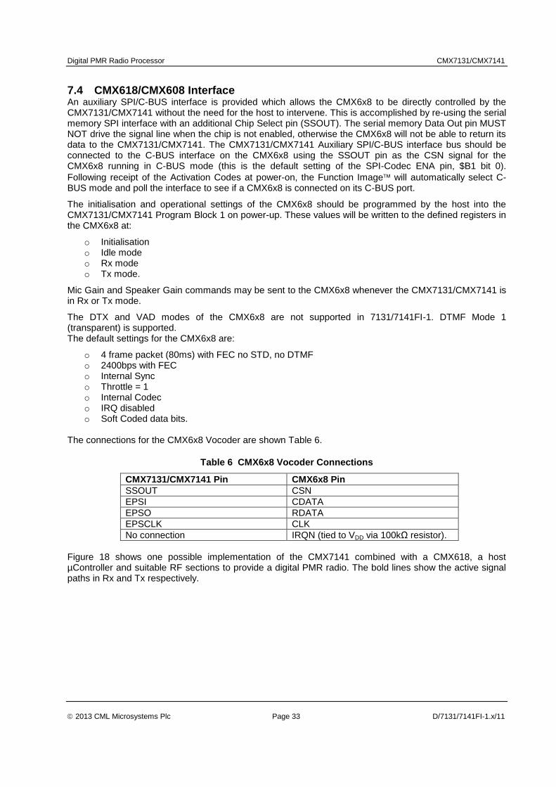
7.4 CMX618/CMX608 Interface An auxiliary SPI/C-BUS interface is provided which allows the CMX6x8 to be directly controlled by the CMX7131/CMX7141 without the need for the host to intervene. This is accomplished by re-using the serial memory SPI interface with an additional Chip Select pin (SSOUT). The serial memory Data Out pin MUST NOT drive the signal line when the chip is not enabled, otherwise the CMX6x8 will not be able to return its data to the CMX7131/CMX7141. The CMX7131/CMX7141 Auxiliary SPI/C-BUS interface bus should be connected to the C-BUS interface on the CMX6x8 using the SSOUT pin as the CSN signal for the CMX6x8 running in C-BUS mode (this is the default setting of the SPI-Codec ENA pin, $B1 bit 0).
Following receipt of the Activation Codes at power-on, the Function Image will automatically select C-BUS mode and poll the interface to see if a CMX6x8 is connected on its C-BUS port.
The initialisation and operational settings of the CMX6x8 should be programmed by the host into the CMX7131/CMX7141 Program Block 1 on power-up. These values will be written to the defined registers in the CMX6x8 at:
o Initialisation o Idle mode o Rx mode o Tx mode.
Mic Gain and Speaker Gain commands may be sent to the CMX6x8 whenever the CMX7131/CMX7141 is in Rx or Tx mode.
The DTX and VAD modes of the CMX6x8 are not supported in 7131/7141FI-1. DTMF Mode 1 (transparent) is supported. The default settings for the CMX6x8 are:
o 4 frame packet (80ms) with FEC no STD, no DTMF o 2400bps with FEC o Internal Sync o Throttle = 1 o Internal Codec o IRQ disabled o Soft Coded data bits.
The connections for the CMX6x8 Vocoder are shown Table 6.
Table 6 CMX6x8 Vocoder Connections
CMX7131/CMX7141 Pin CMX6x8 Pin
SSOUT CSN
EPSI CDATA
EPSO RDATA
EPSCLK CLK
No connection IRQN (tied to VDD via 100kΩ resistor).
Figure 18 shows one possible implementation of the CMX7141 combined with a CMX618, a host µController and suitable RF sections to provide a digital PMR radio. The bold lines show the active signal paths in Rx and Tx respectively.

Digital PMR Radio Processor CMX7131/CMX7141
2013 CML Microsystems Plc Page 34 D/7131/7141FI-1.x/11
CMX618
CMX618
Host
Host
CMX7141
CMX7141
RF Section
Vocoder
Disc
MOD1
MOD2
PAramp
SPI
EEPROM
Interface
C-BUS SCLK
C-BUS CDATA
C-BUS CSN
C-BUS RDATA
Mic
Spkr
modemDe-
coding
RF Section
Vocoder
Disc
MOD1
MOD2
PAramp
C-BUS SCLK
C-BUS CDATA
C-BUS SCLK
C-BUS RDATA
Mic
Spkr
modem coding
Audio
Codec
Audio
Codec
Squelch
RxENA
TxENA
Squelch
RxENA
TxENA
protocol
protocol
SPI
EEPROM
Interface
Figure 18 Digital Voice Rx and Tx Blocks
The paralleling of the microphone and speaker connections between the CMX618 and the CMX7131/CMX7141 is only required if the CMX7131/CMX7141 is also to provide analogue PMR functionality. Otherwise, the microphone and speaker should be connected to the CMX618 only. The CMX618 RALCWI Vocoder provides an on-chip audio and voice codec, but alternatively a CMX608 device could be used along with an external audio codec. Voice payload data is transferred directly from and to the CMX618 by the CMX7131/CMX7141. Note that the CMX618 Audio output does not have a high impedance mode, therefore an external analogue switch is required to isolate it when not required, if the Analogue PMR Function Image™ (7031/7041FI-1.x) is to be used on the device.
Digital PMR Radio Processor CMX7131/CMX7141
2013 CML Microsystems Plc Page 35 D/7131/7141FI-1.x/11
7.5 DVSI Vocoder Interface If the DVSI vocoder (or other third-party vocoder) is used all radio channel data will need to be transferred over the main C-BUS through the host. In this case the Vocoder Enable Program registers (P1.19 and P1.20) should be set appropriately to respond correctly to the incoming data fields and the SPI-Codec ENA bit ($B1 bit 0) should be set to 1. To speed the power-on process, the Automatic presence check for the CMX6x8 may be skipped by setting the SPI-Codec ENA bit BEFORE the activation codes are loaded during the power-on sequence.
The connections for the DVSI vocoder are shown in Table 7.
Table 7 DVSI Vocoder Connections
CMX7131/CMX7141 Pin DVSI Vocoder Pin
SSOUT SPI_STE
EPSI SPI_RX_DATA
EPSO SPI_TX_DATA
EPSCLK SPI_CLK and SPI_CLK_IN.
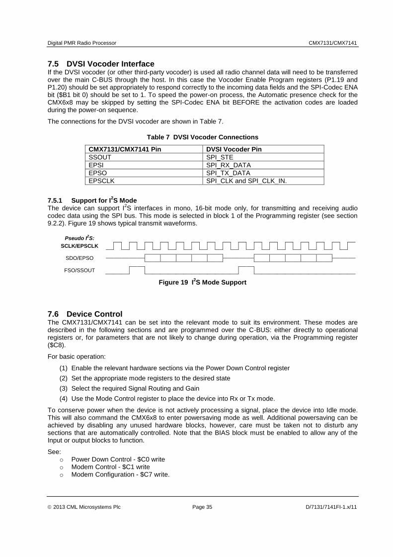
7.5.1 Support for I2S Mode
The device can support I2S interfaces in mono, 16-bit mode only, for transmitting and receiving audio
codec data using the SPI bus. This mode is selected in block 1 of the Programming register (see section 9.2.2). Figure 19 shows typical transmit waveforms.
Pseudo I2S:
SCLK/EPSCLK
SDO/EPSO
FSO/SSOUT
Figure 19 I2S Mode Support
7.6 Device Control The CMX7131/CMX7141 can be set into the relevant mode to suit its environment. These modes are described in the following sections and are programmed over the C-BUS: either directly to operational registers or, for parameters that are not likely to change during operation, via the Programming register ($C8).
For basic operation:
(1) Enable the relevant hardware sections via the Power Down Control register
(2) Set the appropriate mode registers to the desired state
(3) Select the required Signal Routing and Gain
(4) Use the Mode Control register to place the device into Rx or Tx mode.
To conserve power when the device is not actively processing a signal, place the device into Idle mode. This will also command the CMX6x8 to enter powersaving mode as well. Additional powersaving can be achieved by disabling any unused hardware blocks, however, care must be taken not to disturb any sections that are automatically controlled. Note that the BIAS block must be enabled to allow any of the Input or output blocks to function.
See: o Power Down Control - $C0 write o Modem Control - $C1 write o Modem Configuration - $C7 write.
Digital PMR Radio Processor CMX7131/CMX7141
2013 CML Microsystems Plc Page 36 D/7131/7141FI-1.x/11
7.6.1 General Notes In normal operation, the most significant registers, in addition to the TxData and RxData blocks, are:
o Modem Control - $C1 write o IRQ Status - $C6 read o Analogue Output Gain - $B0 write o Input Gain and Signal Routing - $B1 write o AuxData Write - $C2 write o CMX6x8 Analogue Gain- $C3 write
Setting the Mode register to either Rx or Tx will automatically increase the internal clock speed to its operational speed and bring the CMX6x8 out of its powersave mode, whilst setting the Mode register to Idle will automatically return the internal clock to a lower (powersaving) speed. To access the Program Blocks (through the Programming register, $C8) the device MUST be in Idle mode.
Under normal circumstances the CMX7131/CMX7141 manages the Main Clock Control automatically, using the default values loaded in Program Block 3.
7.6.2 Interrupt Operation The CMX7131/CMX7141 will issue an interrupt on the IRQN line when the IRQ bit (bit 15) of the IRQ Status register and the IRQ Mask bit (bit 15) are both set to 1. The IRQ bit is set when the state of the interrupt flag bits in the IRQ Status register change from a 0 to 1 and the corresponding mask bit(s) in the
Interrupt Mask register is(are) set. Enabling an interrupt by setting a mask bit (01) after the corresponding IRQ Status register bit has already been set to 1 will also cause the IRQ bit to be set.
All interrupt flag bits in the IRQ Status register, except the Programming Flag (bit 0), are cleared and the interrupt request is cleared following the command/address phase of a C-BUS read of the IRQ Status register. The Programming Flag bit is set to 1 only when it is permissible to write a new word to the Programming register.
See:
o IRQ Status - $C6 read o Interrupt Mask - $CE write.
Continuous polling of the Status register ($C6) is not recommended due to the increase in response time, host loading and potential digital noise generation due to bus activity. If the host cannot support a fully IRQ driven interface then it should route the IRQ signal to a host IO pin and poll this pin instead.
7.6.3 Signal Routing The CMX7131/CMX7141 offers a flexible routing architecture, with three signal inputs, a choice of two modulator configurations (to suit 2-point modulation or I/Q schemes) and a single audio output.
See: o Input Gain and Signal Routing - $B1 write o Modem Control - $C1 write o Modem Configuration - $C7 write.
The analogue gain/attenuation of each input and output can be set individually, with additional Fine Attenuation control available via the Programming registers in the CMX7131/CMX7141. The Mic. and Speaker gains are set by the CMX6x8, which is controlled through the CMX6x8 Analogue Gain- $C3 write of the CMX7131/CMX7141.
See: o Analogue Output Gain - $B0 write (Tx MOD1 and 2) o Input Gain and Signal Routing - $B1 write (Rx DISC input, Tx MOD1 and 2) o CMX6x8 Analogue Gain- $C3 write (CMX6x8 Mic. and Speaker).
In common with other FIs developed for the CMX7131/CMX7141, this device is equipped with two signal processing paths. Input 1 should be routed to either of the three input sources (ALT, DISC or MIC) which
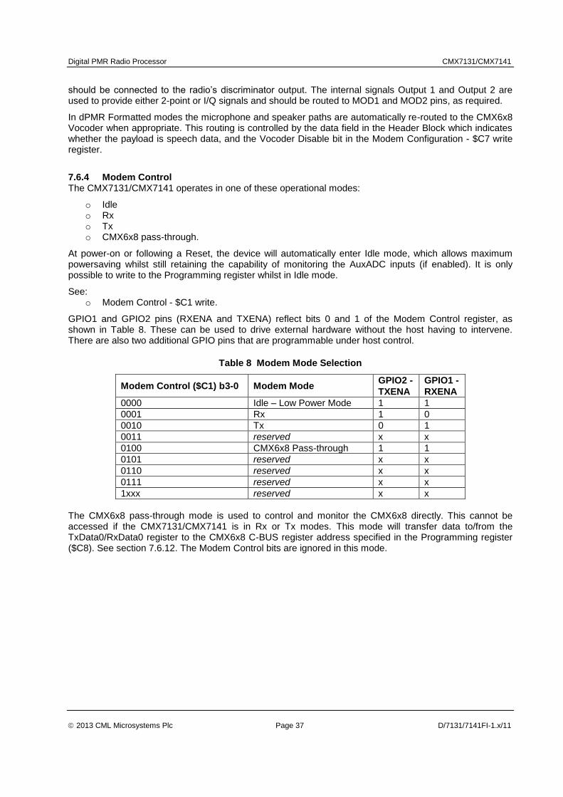
Digital PMR Radio Processor CMX7131/CMX7141
2013 CML Microsystems Plc Page 37 D/7131/7141FI-1.x/11
should be connected to the radio’s discriminator output. The internal signals Output 1 and Output 2 are used to provide either 2-point or I/Q signals and should be routed to MOD1 and MOD2 pins, as required.
In dPMR Formatted modes the microphone and speaker paths are automatically re-routed to the CMX6x8 Vocoder when appropriate. This routing is controlled by the data field in the Header Block which indicates whether the payload is speech data, and the Vocoder Disable bit in the Modem Configuration - $C7 write register.
7.6.4 Modem Control The CMX7131/CMX7141 operates in one of these operational modes:
o Idle o Rx o Tx o CMX6x8 pass-through.
At power-on or following a Reset, the device will automatically enter Idle mode, which allows maximum powersaving whilst still retaining the capability of monitoring the AuxADC inputs (if enabled). It is only possible to write to the Programming register whilst in Idle mode.
See: o Modem Control - $C1 write.
GPIO1 and GPIO2 pins (RXENA and TXENA) reflect bits 0 and 1 of the Modem Control register, as shown in Table 8. These can be used to drive external hardware without the host having to intervene. There are also two additional GPIO pins that are programmable under host control.
Table 8 Modem Mode Selection
Modem Control ($C1) b3-0 Modem Mode GPIO2 -
TXENA
GPIO1 -
RXENA
0000 Idle – Low Power Mode 1 1
0001 Rx 1 0
0010 Tx 0 1
0011 reserved x x
0100 CMX6x8 Pass-through 1 1
0101 reserved x x
0110 reserved x x
0111 reserved x x
1xxx reserved x x
The CMX6x8 pass-through mode is used to control and monitor the CMX6x8 directly. This cannot be accessed if the CMX7131/CMX7141 is in Rx or Tx modes. This mode will transfer data to/from the TxData0/RxData0 register to the CMX6x8 C-BUS register address specified in the Programming register ($C8). See section 7.6.12. The Modem Control bits are ignored in this mode.
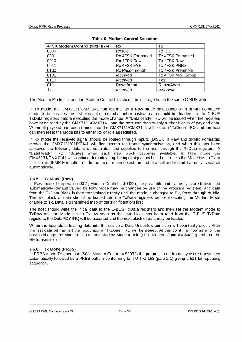
Digital PMR Radio Processor CMX7131/CMX7141
2013 CML Microsystems Plc Page 38 D/7131/7141FI-1.x/11
Table 9 Modem Control Selection
4FSK Modem Control ($C1) b7-4 Rx Tx
0000 Rx Idle Tx Idle
0001 Rx 4FSK Formatted Tx 4FSK Formatted
0010 Rx 4FSK Raw Tx 4FSK Raw
0011 Rx 4FSK EYE Tx 4FSK PRBS
0100 Rx Pass-through Tx 4FSK Preamble
0101 reserved Tx 4FSK Mod Set-up
0110 reserved Test
0111 Reset/Abort Reset/Abort
1xxx reserved reserved
The Modem Mode bits and the Modem Control bits should be set together in the same C-BUS write.
In Tx mode, the CMX7131/CMX7141 can operate as a Raw mode data pump or in dPMR Formatted mode. In both cases the first block of control channel or payload data should be loaded into the C-BUS TxData registers before executing the mode change. A “DataReady” IRQ will be issued when the registers have been read by the CMX7131/CMX7141 and the host can then supply further blocks of payload data. When all payload has been transmitted the CMX7131/CMX7141 will issue a “TxDone” IRQ and the host can then reset the Mode bits to either Rx or Idle as required.
In Rx mode the received signal should be routed through Input1 (DISC). In Raw and dPMR Formatted modes the CMX7131/CMX7141 will first search for frame synchronisation, and when this has been achieved the following data is demodulated and supplied to the host through the RxData registers. A “DataReady” IRQ indicates when each new block becomes available. In Raw mode the CMX7131/CMX7141 will continue demodulating the input signal until the host resets the Mode bits to Tx or Idle, but in dPMR Formatted mode the modem can detect the end of a call and restart frame sync search automatically.
7.6.5 Tx Mode (Raw) In Raw mode Tx operation ($C1, Modem Control = $0022), the preamble and frame sync are transmitted automatically (default values for Raw mode may be changed by use of the Program registers) and data from the TxData Block is then transmitted directly until the mode is changed to Rx, Pass-through or Idle. The first block of data should be loaded into the TxData registers before executing the Modem Mode change to Tx. Data is transmitted msb (most significant bit) first.
The host should write the initial data to the C-BUS TxData registers and then set the Modem Mode to TxRaw and the Mode bits to Tx. As soon as the data block has been read from the C-BUS TxData registers, the DataRDY IRQ will be asserted and the next block of data may be loaded.
When the host stops loading data into the device a Data Underflow condition will eventually occur. After the last data bit has left the modulator a “TxDone” IRQ will be issued. At this point it is now safe for the host to change the Modem Control and Modem Mode to Idle ($C1, Modem Control = $0000) and turn the RF transmitter off.
7.6.6 Tx Mode (PRBS) In PRBS mode Tx operation ($C1, Modem Control = $0032) the preamble and frame sync are transmitted automatically followed by a PRBS pattern conforming to ITU-T O.153 (para 2.1) giving a 511-bit repeating sequence.
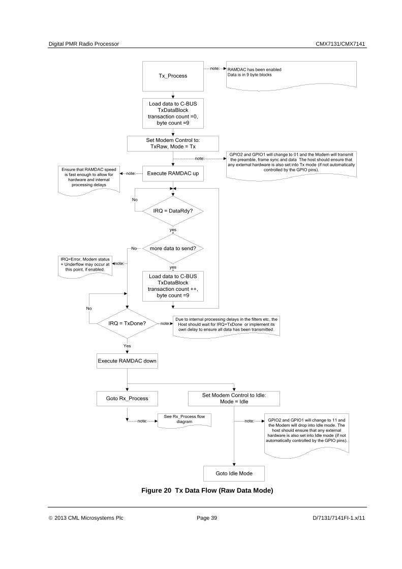
Digital PMR Radio Processor CMX7131/CMX7141
2013 CML Microsystems Plc Page 39 D/7131/7141FI-1.x/11
Load data to C-BUS
TxDataBlock
transaction count =0,
byte count =9
Set Modem Control to:
TxRaw, Mode = Tx
IRQ = DataRdy?
No
GPIO2 and GPIO1 will change to 01 and the Modem will transmit
the preamble, frame sync and data The host should ensure that
any external hardware is also set into Tx mode (if not automatically
controlled by the GPIO pins).
note:
yes
more data to send?
Load data to C-BUS
TxDataBlock
transaction count ++,
byte count =9
yes
No
See Rx_Process flow
diagramnote:
Set Modem Control to Idle:
Mode = Idle
GPIO2 and GPIO1 will change to 11 and
the Modem will drop into Idle mode. The
host should ensure that any external
hardware is also set into Idle mode (if not
automatically controlled by the GPIO pins).
note:
Goto Rx_Process
Goto Idle Mode
RAMDAC has been enabled
Data is in 9 byte blocks
note:
Tx_Process
IRQ = TxDone?
No
Yes
IRQ=Error, Modem status
= Underflow may occur at
this point, if enabled.
note:
Due to internal processing delays in the filters etc, the
Host should wait for IRQ=TxDone or implement its
own delay to ensure all data has been transmitted.
note:
Execute RAMDAC down
Execute RAMDAC upEnsure that RAMDAC speed
is fast enough to allow for
hardware and internal
processing delays
note:
Figure 20 Tx Data Flow (Raw Data Mode)
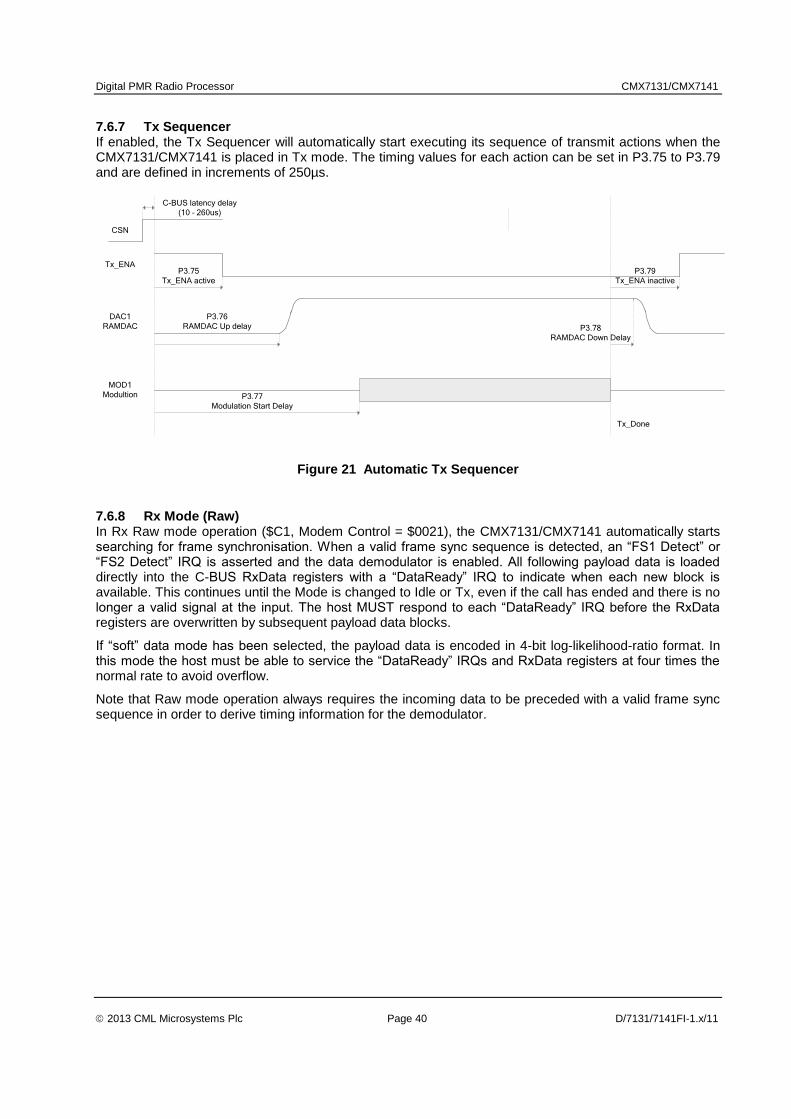
Digital PMR Radio Processor CMX7131/CMX7141
2013 CML Microsystems Plc Page 40 D/7131/7141FI-1.x/11
7.6.7 Tx Sequencer If enabled, the Tx Sequencer will automatically start executing its sequence of transmit actions when the CMX7131/CMX7141 is placed in Tx mode. The timing values for each action can be set in P3.75 to P3.79 and are defined in increments of 250µs.
Tx_ENA
DAC1
RAMDAC
MOD1
Modultion
CSN
Tx_Done
C-BUS latency delay
(10 – 260us)
P3.75
Tx_ENA active
P3.76
RAMDAC Up delay
P3.77
Modulation Start Delay
P3.78
RAMDAC Down Delay
P3.79
Tx_ENA inactive
Figure 21 Automatic Tx Sequencer
7.6.8 Rx Mode (Raw) In Rx Raw mode operation ($C1, Modem Control = $0021), the CMX7131/CMX7141 automatically starts searching for frame synchronisation. When a valid frame sync sequence is detected, an “FS1 Detect” or “FS2 Detect” IRQ is asserted and the data demodulator is enabled. All following payload data is loaded directly into the C-BUS RxData registers with a “DataReady” IRQ to indicate when each new block is available. This continues until the Mode is changed to Idle or Tx, even if the call has ended and there is no longer a valid signal at the input. The host MUST respond to each “DataReady” IRQ before the RxData registers are overwritten by subsequent payload data blocks.
If “soft” data mode has been selected, the payload data is encoded in 4-bit log-likelihood-ratio format. In this mode the host must be able to service the “DataReady” IRQs and RxData registers at four times the normal rate to avoid overflow.
Note that Raw mode operation always requires the incoming data to be preceded with a valid frame sync sequence in order to derive timing information for the demodulator.
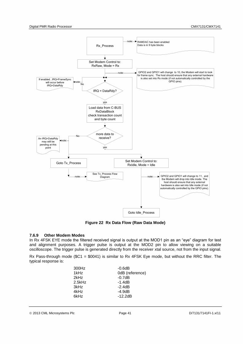
Digital PMR Radio Processor CMX7131/CMX7141
2013 CML Microsystems Plc Page 41 D/7131/7141FI-1.x/11
Rx_Process
Set Modem Control to:
RxRaw, Mode = Rx
IRQ = DataRdy?
No
GPIO2 and GPIO1 will change to 10, the Modem will start to look
for frame sync. The host should ensure that any external hardware
is also set into Rx mode (if not automatically controlled by the
GPIO pins).
note:
yes
more data to
receive?
Load data from C-BUS
RxDataBlock
check transaction count
and byte count
yes
No
See Tx_Process Flow
Diagramnote:
Set Modem Control to:
RxIdle, Mode = Idle
GPIO2 and GPIO1 will change to 11, and
the Modem will drop into Idle mode. The
host should ensure that any external
hardware is also set into Idle mode (if not
automatically controlled by the GPIO pins).
note:
Goto Tx_Process
Goto Idle_Process
RAMDAC has been enabled
Data is in 9 byte blocks
note:
If enabled , IRQ=FrameSync
will occur before
IRQ=DataRdy
note:
An IRQ=DataRdy
may still be
pending at this
point
note:
Figure 22 Rx Data Flow (Raw Data Mode)
7.6.9 Other Modem Modes In Rx 4FSK EYE mode the filtered received signal is output at the MOD1 pin as an “eye” diagram for test and alignment purposes. A trigger pulse is output at the MOD2 pin to allow viewing on a suitable oscilloscope. The trigger pulse is generated directly from the receiver xtal source, not from the input signal.
Rx Pass-through mode ($C1 = $0041) is similar to Rx 4FSK Eye mode, but without the RRC filter. The typical response is:
300Hz -0.6dB 1kHz 0dB (reference) 2kHz -0.7dB 2.5kHz -1.4dB 3kHz -2.4dB 4kHz -4.9dB 6kHz -12.2dB
Digital PMR Radio Processor CMX7131/CMX7141
2013 CML Microsystems Plc Page 42 D/7131/7141FI-1.x/11
In Tx mode a number of test and set-up modes are provided to facilitate test and alignment.
o PRBS (Preamble and Synchronisation Word are automatically transmitted first) o Continuous preamble: a repeating sequence of [+3 +3 -3 -3] symbols o Modulation set-up: in two-point mode, a repeating sequence of eight +3 symbols followed by eight
-3 symbols, and in I/Q mode a continuous sequence of +3 symbols.
7.6.10 Reset/Abort From each mode, a Reset/Abort aborts the current state machine and drops into the corresponding (Rx or Tx) Idle mode. The only difference between this and going directly into the corresponding Idle mode is that all of the buffers and filters are flushed out first with Reset/Abort.
7.6.11 Data Transfer Payload data is transferred from/to the host using blocks of five Rx and five Tx 16-bit C-BUS registers, allowing up to 72 bits (9 bytes) of data to be transferred in sequence. The lowest 8 bits of the register block are reserved for a Byte Counter, Block ID and a Transaction Counter. The byte count indicates how many bytes in the data block are valid and avoids the need to perform a full five word C-BUS read/write if only a smaller block of data need to be transferred.
Table 10 C-BUS Data Registers
C-BUS
Address
Function C-BUS
Address
Function
$B5 Tx data 0-7 and info $B8 Rx data 0-7 and info
$B6 Tx data 8-23 $B9 Rx data 8-23
$B7 Tx data 24-39 $BA Rx data 24-39
$CA Tx data 40-55 $BB Rx data 40-55
$CB Tx data 56-71 $C5 Rx data 56-71
The Block ID in Raw mode must be set to 01 (payload) for consistency with dPMR Formatted mode (see User Manual section 9.1.17).
Bits 7 and 6 hold the Transaction Counter, which is incremented modulo 4 on every read/write of the Data Block to allow detection of data underflow and overflow conditions. In Tx mode the host must increment the counter on every write to the TxData block, and if the CMX7131/CMX7141 identifies that a block has been written out of sequence, the Event bit (C-BUS register $C6, b14) will be asserted and an IRQ raised, if enabled. The device detects that new data from the host is available by the change in the value of the Transaction Counter, therefore the host should ensure that all the data is available in the TxData block before updating this register (ie, it should be the last register the host writes to in any block transfer). In Rx mode, the CMX7131/CMX7141 will automatically increment the counter every time it writes to the RxData block, if the host identifies that a block has been written out of sequence, then it is likely that a data overrun condition has occurred and some data has been lost.
7.6.12 CMX6x8 Pass-through Mode To allow the host to communicate directly with the CMX6x8 for test and configuration purposes, a pass-through mode is available which allows any CMX6x8 C-BUS register to be read or written (as appropriate). This mode uses the TxData0, RxData0 and Programming registers on the CMX7131/CMX7141.
To write to the CMX6x8:
o Set the CMX7131/CMX7141 to CMX6x8 pass-through mode ($C1=$0004) o Wait for the Program Flag to be set ($C6 b0) o Write the CMX6x8 data value to the Txdata0 register ($B5) o Write the CMX6x8 C-BUS address to the Programming register ($C8) with b15=0 o Wait for the Program Flag to be set ($C6 b0).
Digital PMR Radio Processor CMX7131/CMX7141
2013 CML Microsystems Plc Page 43 D/7131/7141FI-1.x/11
To read from the CMX6x8:
o Set the CMX7131/CMX7141 to CMX6x8 pass-through mode ($C1=$0004) o Wait for the Program Flag to be set ($C6 b0) o Write the CMX6x8 C-BUS address to the Programming register ($C8) with b15=1 o Wait for the Program Flag to be set ($C6 b0) o Read the CMX6x8 data value from the RxData0 register ($B8).
CMX6x8 C-BUS addresses are all 8 bits long and should be written to bits 0-7 of the Programming Register. Bit 15 is the read/write flag (0 = read, 1 = write) and bit 14 is the register-size flag (0 = 16-bit, 1 = 8-bit). Unused bits should be cleared to zero. When an 8-bit register is read or written, the data occupies the lower 8 bits of the appropriate data register (TxData0 or RxData0).
7.7 dPMR Formatted Operation In dPMR Formatted mode the CMX7131/CMX7141 performs all frame building/splitting and FEC coding/decoding, which relieves the host controller of a significant processing load. During voice calls the CMX7131/CMX7141 can automatically enable and control the CMX6x8, and transfer voice payload data from/to it without host intervention. In Rx mode the CMX7131/CMX7141 monitors address fields in incoming transmissions and only accepts calls if the programmed address requirements are satisfied. This allows the host to remain in a power-down or “sleep” state until it is really necessary to wake up, extending the battery life of the final product design.
7.7.1 Operating Modes and Addressing TS 102 490 describes two operating modes for a dPMR radio:
o ISF – Initial Services and Facilities – “out of the box” mode o CSF – Configured Services and Facilities – “managed” mode.
The CMX7131/CMX7141 can support either of these modes, as selected by b9 of the Modem Configuration register, $C7 (see User Manual section 9.1.27).
The standard also defines two addressing schemes: 24-bit binary or 7-digit BCD (binary-coded-decimal). Radios operating in ISF mode are required to use binary addressing, but in CSF mode either binary or BCD addressing can be used. Both addressing schemes are supported by the CMX7131/CMX7141, selected by b11 in the Modem Configuration register, $C7 (see User Manual section 9.1.27).
The host can load two Own IDs (binary or BCD) into Program Block 1 for use in both Tx and Rx modes. In Tx mode the host can select which of these to send in the “Caller ID” field of the outgoing call. In Rx mode the CMX7131/CMX7141 compares the “Called ID” field from incoming calls against each of its Own IDs, and will accept the call if a valid ID match is found. Address matching can be disabled using b12 of the Modem Configuration register, $C7 in which case the CMX7131/CMX7141 will accept all incoming calls.
The CMX7131/CMX7141 implements BCD address translation in both Tx and Rx, to relieve the host of the processing required to map BCD digits to over-air binary values. BCD addresses can include wildcard digits in any of the lower four digits, and there are ten BCD “All-Call” addresses with wildcards in all six lower digits. The CMX7131/CMX7141 handles wildcard digits appropriately during address matching in Rx.
Binary addresses do not support group calling with wildcards, but the CMX7131/CMX7141 provides six binary-only Group Call IDs in addition to the two Own IDs. These can be programmed by the host to be used for address matching in Rx only.
TS 102 490 also specifies a system-wide All Call facility using the “Communication Format” field in the Header Frame (TS 102 490 section 5.8). The normal setting for this field is “Peer-to-Peer”, but when set to “Call ALL” the CMX7131/CMX7141 will always accept the call regardless of ISF/CSF mode and all other address settings. The host should take care not to transmit in All Call mode unless actually intended.

Digital PMR Radio Processor CMX7131/CMX7141
2013 CML Microsystems Plc Page 44 D/7131/7141FI-1.x/11
7.7.2 ISF Addressing The services available in ISF mode are described in TS 102 490 section 8.1. Radios using ISF mode provide a style of operation broadly similar to analogue PMR446.
ISF mode requires 24-bit binary addressing to be used, with only the top 8 bits (the Common ID field) in active use for addressing ISF mode devices. The remaining 16 bits must be set to all 1s. This is the default mode of the CMX7131/CMX7141 and the default Common IDs are:
o ID1: $01 o ID2: $02.
The ISF Common All-Call ID is $FF. When in ISF mode the CMX7131/CMX7141 will always accept calls to this address regardless of other address settings.
7.7.3 CSF Addressing The services available in CSF mode are described in TS 102 490 section 8.2 and Annex A.
CSF mode does not mandate BCD addressing unless the host implements the Standard User Interface, but the advantages of BCD addressing are direct mapping of user keypad entries to destination addresses and the option of wildcard digits to implement group calls. The host can select the addressing mode using b11 of the Modem Configuration register, $C7.
7.7.4 Tx Mode (dPMR formatted) Device operation in Tx dPMR Formatted mode ($C1, Modem Control = $0012) is similar to Raw mode operation but the CMX7131/CMX7141 builds Header, Control Channel and End Information blocks, performs all FEC coding, interleaving and scrambling functions and inserts Frame Sync and Colour Code sequences to generate the required frame formats for transmission. During voice calls the CMX7131/CMX7141 can automatically enable and control the CMX6x8, and transfer voice payload data from/to it without host intervention.
The TxData registers are used to transfer Header and End Information fields in addition to payload data. The Block ID field in the TxData0 register informs the CMX7131/CMX7141 how to process each transfer.
b5-4 Block ID
00 HDR - Header Data
01 PLD - Payload Data
10 PLS - Payload Data with Slow Data
11 END - End Data
The host should preload the TxData registers with Header Data before placing the device in Tx dPMR Formatted mode. The CMX7131/CMX7141 reads the “Header Type” field to determine the burst type and then sends the Preamble and Header Frame. If the “Call Information” field indicates that repeated “extended wake-up” Headers are to be sent, the CMX7131/CMX7141 will do so automatically. The Header fields are saved for re-use when building the Control Channel Information blocks in following payload frames: the host does not need to re-load them.
Header Data:
TxData RxData
15 14 13 12 11 10 9 8 7 6 5 4 3 2 1 0
0 LE 0 Own ID Header Type Counter 0 0 1 0 0 1
1 0 0 Call Information Comms Mode
2 Version Format 0 0 0 0 0 0 Colour Code
3 0 0 0 0 Binary mode: Called Address lower 12 bits
BCD mode: Called Address lower 4 digits K4, K5, K6, K7
4 0 0 0 0 Binary mode: Called Address upper 12 bits
0 0 0 0 BCD mode: Called Address upper 3 digits K1, K2, K3
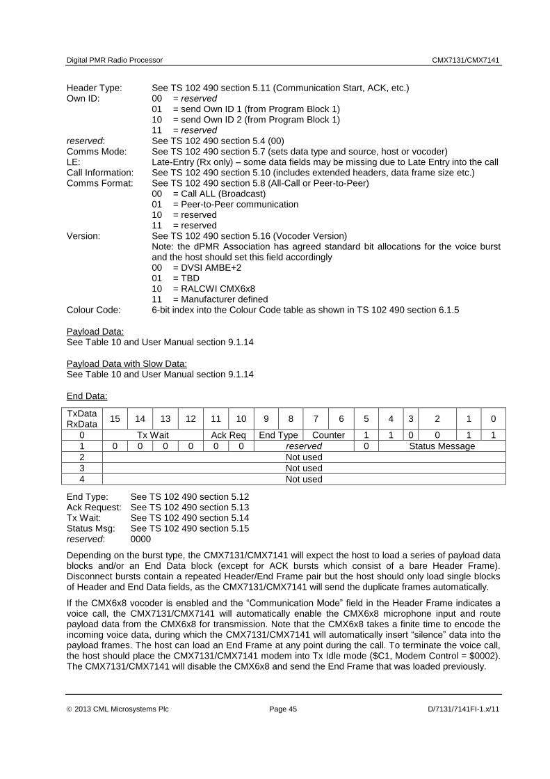
Digital PMR Radio Processor CMX7131/CMX7141
2013 CML Microsystems Plc Page 45 D/7131/7141FI-1.x/11
Header Type: See TS 102 490 section 5.11 (Communication Start, ACK, etc.) Own ID: 00 = reserved 01 = send Own ID 1 (from Program Block 1) 10 = send Own ID 2 (from Program Block 1) 11 = reserved reserved: See TS 102 490 section 5.4 (00) Comms Mode: See TS 102 490 section 5.7 (sets data type and source, host or vocoder) LE: Late-Entry (Rx only) – some data fields may be missing due to Late Entry into the call Call Information: See TS 102 490 section 5.10 (includes extended headers, data frame size etc.) Comms Format: See TS 102 490 section 5.8 (All-Call or Peer-to-Peer)
00 = Call ALL (Broadcast) 01 = Peer-to-Peer communication 10 = reserved 11 = reserved
Version: See TS 102 490 section 5.16 (Vocoder Version) Note: the dPMR Association has agreed standard bit allocations for the voice burst and the host should set this field accordingly 00 = DVSI AMBE+2 01 = TBD 10 = RALCWI CMX6x8 11 = Manufacturer defined
Colour Code: 6-bit index into the Colour Code table as shown in TS 102 490 section 6.1.5
Payload Data: See Table 10 and User Manual section 9.1.14
Payload Data with Slow Data: See Table 10 and User Manual section 9.1.14
End Data:
TxData RxData
15 14 13 12 11 10 9 8 7 6 5 4 3 2 1 0
0 Tx Wait Ack Req End Type Counter 1 1 0 0 1 1
1 0 0 0 0 0 0 reserved 0 Status Message
2 Not used
3 Not used
4 Not used
End Type: See TS 102 490 section 5.12 Ack Request: See TS 102 490 section 5.13 Tx Wait: See TS 102 490 section 5.14 Status Msg: See TS 102 490 section 5.15 reserved: 0000
Depending on the burst type, the CMX7131/CMX7141 will expect the host to load a series of payload data blocks and/or an End Data block (except for ACK bursts which consist of a bare Header Frame). Disconnect bursts contain a repeated Header/End Frame pair but the host should only load single blocks of Header and End Data fields, as the CMX7131/CMX7141 will send the duplicate frames automatically.
If the CMX6x8 vocoder is enabled and the “Communication Mode” field in the Header Frame indicates a voice call, the CMX7131/CMX7141 will automatically enable the CMX6x8 microphone input and route payload data from the CMX6x8 for transmission. Note that the CMX6x8 takes a finite time to encode the incoming voice data, during which the CMX7131/CMX7141 will automatically insert “silence” data into the payload frames. The host can load an End Frame at any point during the call. To terminate the voice call, the host should place the CMX7131/CMX7141 modem into Tx Idle mode ($C1, Modem Control = $0002). The CMX7131/CMX7141 will disable the CMX6x8 and send the End Frame that was loaded previously.
Digital PMR Radio Processor CMX7131/CMX7141
2013 CML Microsystems Plc Page 46 D/7131/7141FI-1.x/11
At the end of all dPMR transmissions the CMX7131/CMX7141 will issue a TxDone IRQ when it is safe for the host to place the device back into Idle mode ($C1, Modem Control = $0000).
7.7.5 Rx Mode (dPMR formatted) Device operation in Rx dPMR Formatted mode ($C1, Modem Control = $0011) is similar to Raw mode operation but the CMX7131/CMX7141 automatically splits incoming calls to extract Header Information, Control Channel Information and End Information blocks and performs all the necessary de-scrambling, de-interleaving and FEC decoding functions. In speech calls the CMX7131/CMX7141 can automatically enable the CMX6x8 vocoder when required and transfer received speech data without host intervention.
The RxData registers are used to transfer Header and End Data fields in addition to payload data. The Block ID field in the RxData0 register informs the host what type of data block each transfer contains. The field layout in the RxData registers for the different transfer types is the same as for Tx dPMR Formatted mode (section 7.7.4).
When placed in Rx dPMR Formatted mode the CMX7131/CMX7141 automatically starts searching for the dPMR frame sync sequences. In addition to detecting the 48-bit FS1 frame sync at the start of a transmission, the CMX7131/CMX7141 can also perform “late entry” into a call by detecting two successive copies of the 24-bit FS2 sequence at the correct two-frame spacing. When a valid frame sync sequence has been detected, an “FS1 Detect” or “FS2 Detect” IRQ is issued and the data demodulator is enabled.
The CMX7131/CMX7141 then decodes the contents of the Header Frame (after an FS1 detect) or the following four Control Channel Information blocks (after an FS2 detect). The Header Information or Control Channel Information CRCs are checked and processing continues only if a full set of valid fields has been received. Header Frames contain two duplicate Header Information blocks: the CMX7131/CMX7141 checks both block CRCs, uses the first valid block and discards the other.
When repeated “extended wake-up” Header Frames are received (see TS 102 490 section 11.1) the CMX7131/CMX7141 will decode the first valid Header but delay address checking until all following repeat Headers have been received. This maximises the time the host can be kept in powersave.
Address checking now takes place depending on ISF/CSF mode and the addressing mode selected. The “Communications Format” field is checked first: if this is set to “Call ALL” the call is accepted. If not, the “Called station ID” is checked against the device’s Own IDs (programmed by the host into Program Block 1) and if a match is found the call is accepted. In ISF mode the Common All-Call ID $FF is also always accepted. In any of these cases a “Called” IRQ is issued to the host, otherwise the call is dropped with no further host notification and the CMX7131/CMX7141 returns to frame sync search. Address matching can be disabled by setting b12 of the Modem Configuration register, in which case the CMX7131/CMX7141 will accept all incoming calls.
The Header fields are presented to the host in the RxData block. Late entry is indicated by bit 15 of RxData1: in this case the “Header Type” and “Call Information” fields in the Header Data block returned to the host will not contain valid data, as these fields are only sent in Header Frames and are not re-sent in the Control Channel Information blocks during a call.
Depending on the burst type the CMX7131/CMX7141 will decode the following payload and/or End Frames and present their contents to the host or vocoder. If the CMX6x8 Vocoder is enabled and the “Communication Mode” field in the Header Frame indicates a voice call, the CMX7131/CMX7141 will automatically enable the CMX6x8 speaker output and route payload data to the CMX6x8 for decoding. In this mode, the data is transferred in 4-bit Log-Likelihood-Ratio format. Otherwise payload data is presented to the host in the RxData registers in soft or hard format as specified. When an End Frame is received the CMX7131/CMX7141 will report its contents to the host, disable the vocoder (if necessary) and return to frame sync search.
All frame sync sequences, Colour Codes and CRCs contained in payload superframes are checked and an “Event” IRQ is issued when any are received incorrectly. If all the frame sync sequences, Colour Codes and CRCs in a superframe are received incorrectly, the superframe is considered corrupt. The host can set a threshold for consecutive corrrupt superframes (in Program Block 0) after which the CMX7131/CMX7141 will issue an “Event” IRQ, drop the call and return to frame sync search.
Digital PMR Radio Processor CMX7131/CMX7141
2013 CML Microsystems Plc Page 47 D/7131/7141FI-1.x/11
See: o RxData 0 - $B8 read o AuxData Read - $CC read.
7.7.6 Slow Data Slow Data may be transferred in voice calls alongside Voice Payload Data, by setting the Block ID to “Payload with Slow Data” and using the AuxData registers. If the CMX6x8 is enabled, there will be no voice payload transfers and so dummy payload transfers are used with the Byte Counter field cleared to zero. In Type1 and Type 2 Data calls the Slow Data field is used to control the data flow over-air and so is generated or decoded by the CMX7131/CMX7141 itself and the only data field that is visible to the host is the “Format” field as defined in TS 102 490 section 5.9.2 which is made available, or supplied by the host, in the lowest 4 bits of the AuxData register.
In Tx mode:
o Load AuxData register with two bytes of Slow Data: AuxData Write - $C2 write o Set Communications Mode to “Voice with Slow Data” o Set first BlockID to “Payload with Slow Data”: TxData 0 - $B5 write
(subsequent blocks should be marked as “Payload Data”: TxData 0 - $B5 write) o Set Byte Counter field (to zero if CMX6x8 is in use): TxData 0 - $B5 write.
The CMX7131/CMX7141 has an internal 64-byte buffer for Slow Data. While the host keeps this internal data buffer “topped-up” the CMX7131/CMX7141 will continue to transmit Slow Data and add the “continuation bits” to the over-air data. Note that only two bytes of Slow Data are sent over-air for every 36 bytes of voice payload, so the buffer may overflow if a large quantity of Slow Data is loaded continuously. An IRQ bit will be raised when there are only two bytes left in the FIFO.
When the host allows the internal buffer to empty, the CMX7131/CMX7141 will terminate the transmission of Slow Data in the current burst. It is not possible to re-start Slow Data transmission within a burst.
In Rx mode:
o BlockID will report “Payload with Slow Data”: RxData 0 - $B8 read o Communications Mode will report “Voice with Slow Data” o If payload is being sent to the CMX6x8, then the Byte Counter field will be cleared to zero o Slow Data is available in the AuxData register: AuxData Read - $CC read.
When the Slow Data transfer has completed, the CMX7131/CMX7141 will stop presenting data to the host.
7.8 Squelch Operation Many Limiter/Discriminator chips provide a noise-quieting squelch circuit around an op-amp configured as a filter. This signal is conventionally passed to a comparator to provide a digital squelch signal, which can be routed directly to one of the CMX7131/CMX7141’s GPIO pins or to the host. However with the CMX7131/CMX7141, the comparator and threshold operations can be replaced by one of the AuxADCs with programmable thresholds and hysteresis functions.
See: o IRQ Status - $C6 read o Modem Configuration - $C7 write.
7.9 GPIO Pin Operation The CMX7131/CMX7141 provides 4 pins: GPIO1, GPIO2, GPIOA and GPIOB. RXENA (GPIO1) and TXENA (GPIO2) are configured to reflect the Tx/Rx state of the Mode register (TXENA and RXENA, active low).
See: o Modem Configuration - $C7 write.

Digital PMR Radio Processor CMX7131/CMX7141
2013 CML Microsystems Plc Page 48 D/7131/7141FI-1.x/11
Note that RXENA and TXENA will not change state until the relevant mode change has been executed by the CMX7131/CMX7141. This is to allow the host sufficient time to load the relevant data buffers and the CMX7131/CMX7141 time to encode the data required prior to its transmission. There is thus a fixed time delay between the GPIO pins changing state and the data signal appearing at the MOD output pins. During the power-on sequence (until the FI has completed its load sequence) these pins have only a weak pull-up applied to them, so care should be taken to ensure that any loading during this period does not adversely affect the operation of the unit.
GPIOA and GPIOB are host programmable for input or output using the AuxADC Configuration register, $A7. The default state is output, high level. When set for input, the values can be read back using the Modem Status register, $C9.
7.10 Auxiliary ADC Operation The inputs to the two auxiliary ADCs can be independently routed from any of the signal input pins under control of the AuxADC Configuration register, $A7. Conversions will be performed as long as a valid input source is selected. To stop the ADCs, the input source should be set to “off”. Register $C0, b6, BIAS, must be enabled for auxiliary ADC operation.
Averaging can be applied to the ADC readings by selecting the relevant bits in the AuxADC Configuration register, $A7, the length of the averaging is determined by the value in the Programming register (P3.0 and P3.1), and defaults to a value of 0. This is a rolling average system such that a proportion of the current data will be added to the last average value. The proportion is determined by the value of the average counter in P3.0 and P3.1.
For an average value of:
0 = 50% of the current value will be added to 50% of the last average value,
1 = 25% of the current value will be added to 75% of the last average value,
2 = 12.5% etc.
The maximum useful value of this field is 9.
High and Low thresholds may be independently applied to both ADC channels (the comparison is applied after averaging, if this is enabled) and an IRQ generated when a rising edge passes the High threshold or a falling edge passes the Low threshold, see Figure 23. The thresholds are programmed via the AuxADC Threshold register, $CD. See Figure 23.
Signal
IRQIRQIRQIRQ
High
Threshold
Low
Threshold
Figure 23 AuxADC IRQ Operation

Digital PMR Radio Processor CMX7131/CMX7141
2013 CML Microsystems Plc Page 49 D/7131/7141FI-1.x/11
Auxiliary ADC data is read back in the AuxADC Data registers ($A9 and $AA) and includes the threshold status as well as the actual conversion data (subject to averaging, if enabled).
See: o AuxADC Configuration - $A7 write o AuxADC1 Data and Status - $A9 read o AuxADC2 Data and Status - $AA read o AuxADC Threshold Data - $CD write.
7.11 Auxiliary DAC/RAMDAC Operation The four auxiliary DAC channels are programmed via the AuxDAC Data/Control register, $A8. AuxDAC channel 1 may also be programmed to operate as a RAMDAC which will automatically output a pre-programmed profile at a programmed rate. The AuxDAC Data/Control register, $A8, with b12 set, controls this mode of operation. The default profile is a raised cosine (see Table 15), but this may be over-written with a user-defined profile by writing to Programming register P3.11. The RAMDAC operation is only available in Tx mode and, to avoid glitches in the ramp profile, it is important not to change to Idle or Rx mode whilst the RAMDAC is still ramping. The AuxDAC outputs hold the user-programmed level during a powersave operation if left enabled, otherwise they will return to zero. Note that access to all four AuxDACs is controlled by the AuxDAC Data/Control register, $A8, and therefore to update all AuxDACs requires four writes to this register. It is not possible to simultaneously update all four AuxDACs.
See: o AuxDAC Data/Control - $A8 write.
7.12 RF Synthesiser (CMX7131 only) The CMX7131 includes two Integer-N RF synthesisers, each comprising a divider, phase comparator and charge pump. The divider has two sets of N and R registers: one set can be used for transmit and the other for receive. The division ratios can be set up in advance by means of C-BUS registers. A single C-BUS command will change over from the transmit to the receive division ratios, or vice versa, enabling a fast turnaround.
See: o RF Synthesiser Data - $B2 write o RF Synthesiser Control - $B3 write o RF Synthesiser Status - $B4 8-bit read.
External RF components are needed to complete the synthesiser circuit. A typical schematic for a 446MHz synthesiser (3.125kHz comparison frequency) is shown in Figure 24.
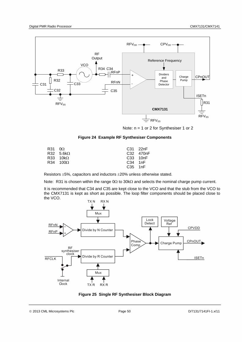
Digital PMR Radio Processor CMX7131/CMX7141
2013 CML Microsystems Plc Page 50 D/7131/7141FI-1.x/11
CMX7131
+
-
RF
Output
RFnP
RFnN
RFVSS
RFVDD CPVDD
Charge
Pump
Dividers
and
Phase
Detector
RFVSS
R31RFVSS
VCO
C35
C34R33
C33
C32
R32C31
CPnOUT
ISETn
Reference Frequency
Note: n = 1 or 2 for Synthesiser 1 or 2
R34
Figure 24 Example RF Synthesiser Components
R31 0 C31 22nF R32 5.6k C32 470nF R33 10k C33 10nF R34 100 C34 1nF
C35 1nF
Resistors 5%, capacitors and inductors 20% unless otherwise stated.
Note: R31 is chosen within the range 0 to 30k and selects the nominal charge pump current.
It is recommended that C34 and C35 are kept close to the VCO and that the stub from the VCO to the CMX7131 is kept as short as possible. The loop filter components should be placed close to the VCO.
Figure 25 Single RF Synthesiser Block Diagram
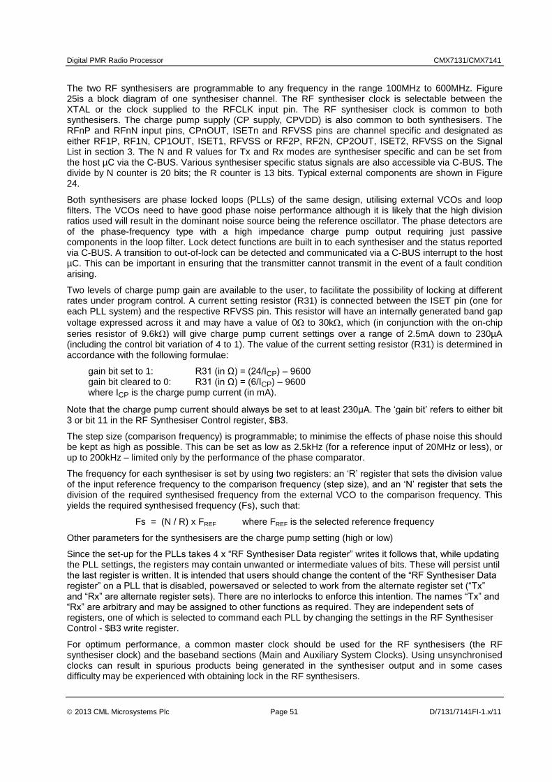
Digital PMR Radio Processor CMX7131/CMX7141
2013 CML Microsystems Plc Page 51 D/7131/7141FI-1.x/11
The two RF synthesisers are programmable to any frequency in the range 100MHz to 600MHz. Figure 25is a block diagram of one synthesiser channel. The RF synthesiser clock is selectable between the XTAL or the clock supplied to the RFCLK input pin. The RF synthesiser clock is common to both synthesisers. The charge pump supply (CP supply, CPVDD) is also common to both synthesisers. The RFnP and RFnN input pins, CPnOUT, ISETn and RFVSS pins are channel specific and designated as either RF1P, RF1N, CP1OUT, ISET1, RFVSS or RF2P, RF2N, CP2OUT, ISET2, RFVSS on the Signal List in section 3. The N and R values for Tx and Rx modes are synthesiser specific and can be set from the host µC via the C-BUS. Various synthesiser specific status signals are also accessible via C-BUS. The divide by N counter is 20 bits; the R counter is 13 bits. Typical external components are shown in Figure 24.
Both synthesisers are phase locked loops (PLLs) of the same design, utilising external VCOs and loop filters. The VCOs need to have good phase noise performance although it is likely that the high division ratios used will result in the dominant noise source being the reference oscillator. The phase detectors are of the phase-frequency type with a high impedance charge pump output requiring just passive components in the loop filter. Lock detect functions are built in to each synthesiser and the status reported via C-BUS. A transition to out-of-lock can be detected and communicated via a C-BUS interrupt to the host µC. This can be important in ensuring that the transmitter cannot transmit in the event of a fault condition arising.
Two levels of charge pump gain are available to the user, to facilitate the possibility of locking at different rates under program control. A current setting resistor (R31) is connected between the ISET pin (one for each PLL system) and the respective RFVSS pin. This resistor will have an internally generated band gap
voltage expressed across it and may have a value of 0 to 30k, which (in conjunction with the on-chip
series resistor of 9.6k) will give charge pump current settings over a range of 2.5mA down to 230µA (including the control bit variation of 4 to 1). The value of the current setting resistor (R31) is determined in accordance with the following formulae:
gain bit set to 1: R31 (in Ω) = (24/ICP) – 9600 gain bit cleared to 0: R31 (in Ω) = (6/ICP) – 9600 where ICP is the charge pump current (in mA).
Note that the charge pump current should always be set to at least 230µA. The ‘gain bit’ refers to either bit 3 or bit 11 in the RF Synthesiser Control register, $B3.
The step size (comparison frequency) is programmable; to minimise the effects of phase noise this should be kept as high as possible. This can be set as low as 2.5kHz (for a reference input of 20MHz or less), or up to 200kHz – limited only by the performance of the phase comparator.
The frequency for each synthesiser is set by using two registers: an ‘R’ register that sets the division value of the input reference frequency to the comparison frequency (step size), and an ‘N’ register that sets the division of the required synthesised frequency from the external VCO to the comparison frequency. This yields the required synthesised frequency (Fs), such that:
Fs = (N / R) x FREF where FREF is the selected reference frequency
Other parameters for the synthesisers are the charge pump setting (high or low)
Since the set-up for the PLLs takes 4 x “RF Synthesiser Data register” writes it follows that, while updating the PLL settings, the registers may contain unwanted or intermediate values of bits. These will persist until the last register is written. It is intended that users should change the content of the “RF Synthesiser Data register” on a PLL that is disabled, powersaved or selected to work from the alternate register set (“Tx” and “Rx” are alternate register sets). There are no interlocks to enforce this intention. The names “Tx” and “Rx” are arbitrary and may be assigned to other functions as required. They are independent sets of registers, one of which is selected to command each PLL by changing the settings in the RF Synthesiser Control - $B3 write register.
For optimum performance, a common master clock should be used for the RF synthesisers (the RF synthesiser clock) and the baseband sections (Main and Auxiliary System Clocks). Using unsynchronised clocks can result in spurious products being generated in the synthesiser output and in some cases difficulty may be experienced with obtaining lock in the RF synthesisers.
Digital PMR Radio Processor CMX7131/CMX7141
2013 CML Microsystems Plc Page 52 D/7131/7141FI-1.x/11
Lock Status The lock status can be observed by reading the RF Synthesiser Status register, $B4, and the individual lock status bits can (subject to masking) provide a C-BUS interrupt.
The lock detector can use a tolerance of one cycle or four cycles of the reference clock (not the divided version that is used as a comparison frequency) in order to judge phase lock. An internal shift register holds the last three lock status measurements and the lock status bits are flagged according to a majority vote of these previous three states. Hence, one occasional lock error will not flag a lock fail. At least two successive phase lock events are required for the lock status to be true. Note that the lock status bits confirm phase lock to the measured tolerance and not frequency lock. The synthesiser may take more time to confirm phase lock with the lock status bits than the time to switch from channel to channel. The purpose of a 4-cycle tolerance is for the case where a high frequency reference oscillator would not forgive a small phase error.
RF Inputs The RF inputs are differential and self-biased (when not powersaved). They are intended to be capacitatively coupled to the RF signal. The signal should be in the range 0dBm to –20dBm (not necessarily balanced). To ensure an accurate input signal the RF should be terminated with 50Ω as close to the chip as possible and with the “P” and “N“ inputs capacitatively coupled to the input and ground, keeping these connections as short as possible. The RF input impedance is almost purely capacitative and is dominated by package and printed circuit board parasitics.
Guidelines for using the RF Synthesisers
RF input slew rate (dv/dt) should be 14 V/µs minimum.
The RF Synthesiser 2.5V digital supply can be powered from the VDEC output pin.
RF clock sources and other, different clock sources must not share common IC components, as this may introduce coupling into the RF. Unused ac-coupled clock buffer circuits should be tied off to a dc supply, to prevent them oscillating.
It is recommended that the RF Synthesisers are operated with maximum charge pump gain (ie. ISET tied to RFVSS).
The loop filter components should be optimised for each VCO.
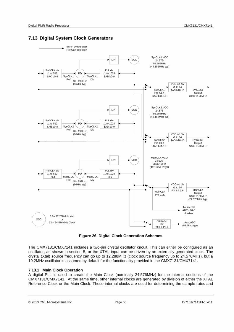
Digital PMR Radio Processor CMX7131/CMX7141
2013 CML Microsystems Plc Page 53 D/7131/7141FI-1.x/11
7.13 Digital System Clock Generators
Ref CLK div
/1 to 512
$AC b0-8
PD
VCO
PLL div
/1 to 1024
$AB b0-9
LPF
SysCLK1
Ref
SysCLK1
Div
VCO op div
/1 to 64
$AB b10-15SysCLK1
Pre-CLK
$AC b11-15
SysCLK1
Output
384kHz-20MHz
48 - 192kHz
(96kHz typ)
SysCLK1 VCO
24.576-
98.304MHz
(49.152MHz typ)
Ref CLK div
/1 to 512
$AE b0-8
PD
VCO
PLL div
/1 to 1024
$AD b0-9
LPF
SysCLK2
Ref
SysCLK2
Div
VCO op div
/1 to 64
$AD b10-15SysCLK2
Pre-CLK
$AE b11-15
SysCLK2
Output
384kHz-20MHz
48 - 192kHz
(96kHz typ)
SysCLK2 VCO
24.576-
98.304MHz
(49.152MHz typ)
Ref CLK div
/1 to 512
P3.4
PD
VCO
PLL div
/1 to 1024
P3.5
LPF
MainCLK
Ref
MainCLK
Div
VCO op div
/1 to 64
P3.3 & 3.6MainCLK
Pre-CLK
MainCLK
Output
384kHz-50MHz
(24.576MHz typ)
48 - 192kHz
(96kHz typ)
MainCLK VCO
24.576-
98.304MHz
(49.152MHz typ)
To Internal
ADC / DAC
dividers
AuxADC
Div
P3.3 & P3.6
Aux_ADC
(83.3kHz typ)
OSC
3.0 - 12.288MHz Xtal
or
3.0 - 24.576MHz Clock
to RF Synthesiser
Ref CLK selection
Figure 26 Digital Clock Generation Schemes
The CMX7131/CMX7141 includes a two-pin crystal oscillator circuit. This can either be configured as an oscillator, as shown in section 5, or the XTAL input can be driven by an externally generated clock. The crystal (Xtal) source frequency can go up to 12.288MHz (clock source frequency up to 24.576MHz), but a 19.2MHz oscillator is assumed by default for the functionality provided in the CMX7131/CMX7141.
7.13.1 Main Clock Operation A digital PLL is used to create the Main Clock (nominally 24.576MHz) for the internal sections of the CMX7131/CMX7141. At the same time, other internal clocks are generated by division of either the XTAL Reference Clock or the Main Clock. These internal clocks are used for determining the sample rates and
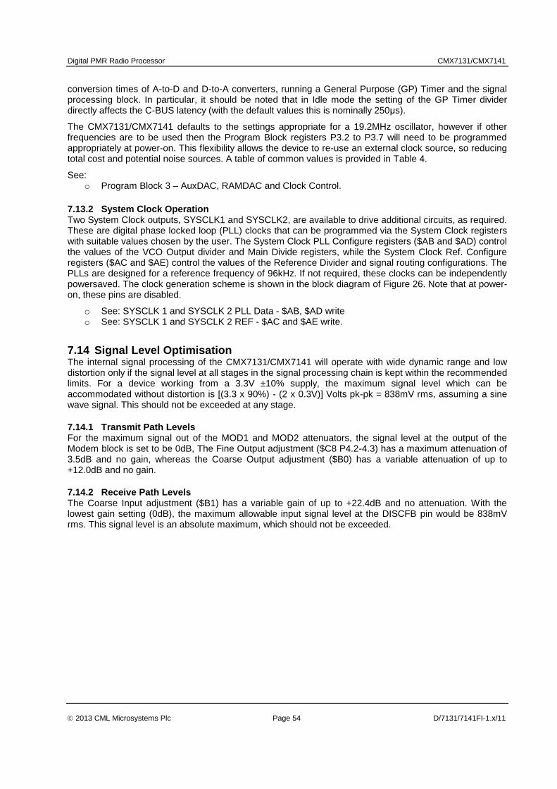
Digital PMR Radio Processor CMX7131/CMX7141
2013 CML Microsystems Plc Page 54 D/7131/7141FI-1.x/11
conversion times of A-to-D and D-to-A converters, running a General Purpose (GP) Timer and the signal processing block. In particular, it should be noted that in Idle mode the setting of the GP Timer divider directly affects the C-BUS latency (with the default values this is nominally 250μs).
The CMX7131/CMX7141 defaults to the settings appropriate for a 19.2MHz oscillator, however if other frequencies are to be used then the Program Block registers P3.2 to P3.7 will need to be programmed appropriately at power-on. This flexibility allows the device to re-use an external clock source, so reducing total cost and potential noise sources. A table of common values is provided in Table 4.
See: o Program Block 3 – AuxDAC, RAMDAC and Clock Control.
7.13.2 System Clock Operation Two System Clock outputs, SYSCLK1 and SYSCLK2, are available to drive additional circuits, as required. These are digital phase locked loop (PLL) clocks that can be programmed via the System Clock registers with suitable values chosen by the user. The System Clock PLL Configure registers ($AB and $AD) control the values of the VCO Output divider and Main Divide registers, while the System Clock Ref. Configure registers ($AC and $AE) control the values of the Reference Divider and signal routing configurations. The PLLs are designed for a reference frequency of 96kHz. If not required, these clocks can be independently powersaved. The clock generation scheme is shown in the block diagram of Figure 26. Note that at power-on, these pins are disabled.
o See: SYSCLK 1 and SYSCLK 2 PLL Data - $AB, $AD write o See: SYSCLK 1 and SYSCLK 2 REF - $AC and $AE write.
7.14 Signal Level Optimisation The internal signal processing of the CMX7131/CMX7141 will operate with wide dynamic range and low distortion only if the signal level at all stages in the signal processing chain is kept within the recommended limits. For a device working from a 3.3V ±10% supply, the maximum signal level which can be accommodated without distortion is [(3.3 x 90%) - (2 x 0.3V)] Volts pk-pk = 838mV rms, assuming a sine wave signal. This should not be exceeded at any stage.
7.14.1 Transmit Path Levels For the maximum signal out of the MOD1 and MOD2 attenuators, the signal level at the output of the Modem block is set to be 0dB, The Fine Output adjustment ($C8 P4.2-4.3) has a maximum attenuation of 3.5dB and no gain, whereas the Coarse Output adjustment ($B0) has a variable attenuation of up to +12.0dB and no gain.
7.14.2 Receive Path Levels The Coarse Input adjustment ($B1) has a variable gain of up to +22.4dB and no attenuation. With the lowest gain setting (0dB), the maximum allowable input signal level at the DISCFB pin would be 838mV rms. This signal level is an absolute maximum, which should not be exceeded.
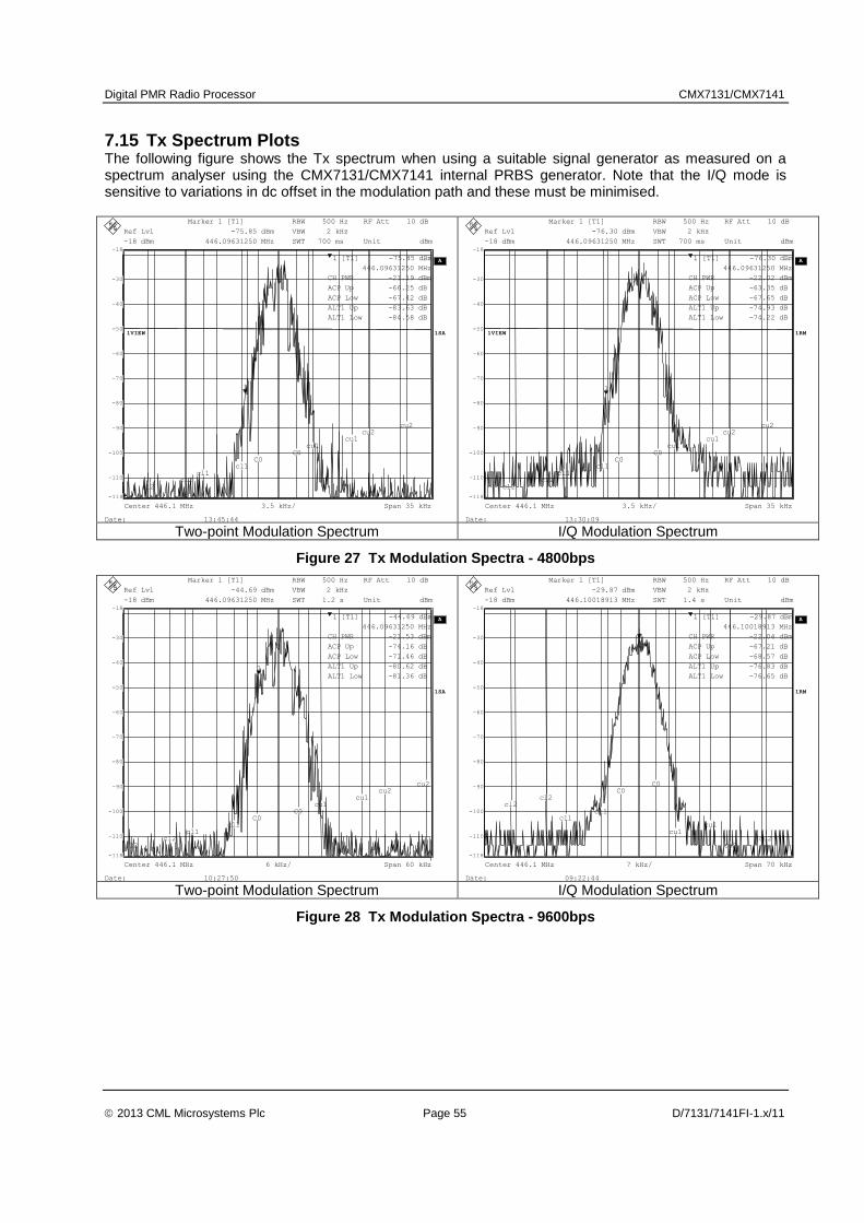
Digital PMR Radio Processor CMX7131/CMX7141
2013 CML Microsystems Plc Page 55 D/7131/7141FI-1.x/11
7.15 Tx Spectrum Plots The following figure shows the Tx spectrum when using a suitable signal generator as measured on a spectrum analyser using the CMX7131/CMX7141 internal PRBS generator. Note that the I/Q mode is sensitive to variations in dc offset in the modulation path and these must be minimised.
R e f
L v l
- 1 8 d B m
R e f L v l
- 1 8 d B m
R B W 5 0 0
H z
V B W 2 k H z
S W T 7 0 0
m s
R F A t t
1 0 d B
A
U n i t d B m
3 . 5 k H z / C e n t e r 4 4 6 . 1
M H z S p a n 3 5
k H z
1 V I E W 1 S A
- 1 1 0
- 1 0 0
- 9 0
- 8 0
- 7 0
- 6 0
- 5 0
- 4 0
- 3 0
- 1 1 8
- 1 8
1
M a r k e r 1 [ T 1 ]
- 7 5 . 8 5 d B m
4 4 6 . 0 9 6 3 1 2 5 0
M H z
1 [ T 1 ]
- 7 5 . 8 5
d B m
4 4 6 . 0 9 6 3 1 2 5 0
M H z
C H P W R
- 2 1 . 1 9
d B m
A C P U p
- 6 6 . 2 5 d B A C P
L o w
- 6 7 . 4 2
d B A L T 1
U p
- 8 3 . 6 3 d B A L T 1
L o w
- 8 4 . 5 8
d B
c l 2 c l 2
c l 1 c l 1 C 0
C 0 c u 1
c u 1 c u 2
c u 2
D a t e :
1 3 : 4 5 : 4 4
R e f
L v l
- 1 8 d B m
R e f L v l
- 1 8 d B m
R B W 5 0 0
H z
S W T 7 0 0
m s
R F A t t
1 0 d B
A
U n i t d B m
3 . 5 k H z / C e n t e r 4 4 6 . 1
M H z S p a n 3 5
k H z
V B W 2 k H z
1 V I E W 1 R M
- 1 1 0
- 1 0 0
- 9 0
- 8 0
- 7 0
- 6 0
- 5 0
- 4 0
- 3 0
- 1 1 8
- 1 8
1
M a r k e r 1 [ T 1 ]
- 7 6 . 3 0 d B m
4 4 6 . 0 9 6 3 1 2 5 0
M H z
1 [ T 1 ]
- 7 6 . 3 0
d B m
4 4 6 . 0 9 6 3 1 2 5 0
M H z
C H P W R
- 2 2 . 0 2
d B m
A C P U p
- 6 3 . 3 5 d B A C P
L o w
- 6 7 . 6 5
d B A L T 1
U p
- 7 4 . 9 3 d B A L T 1
L o w
- 7 4 . 2 2
d B
c l 2 c l 2
c l 1 c l 1 C 0
C 0 c u 1
c u 1 c u 2
c u 2
D a t e :
1 3 : 3 0 : 0 9 Two-point Modulation Spectrum I/Q Modulation Spectrum
Figure 27 Tx Modulation Spectra - 4800bps
R e f
L v l
- 1 8 d B m
R e f L v l
- 1 8 d B m
R B W 5 0 0
H z
V B W 2 k H z
S W T 1 . 2
s
R F A t t
1 0 d B
A
1 S A
U n i t d B m
6 k H z / C e n t e r 4 4 6 . 1
M H z S p a n 6 0
k H z
- 1 1 0
- 1 0 0
- 9 0
- 8 0
- 7 0
- 6 0
- 5 0
- 4 0
- 3 0
- 1 1 8
- 1 8
1
M a r k e r 1 [ T 1 ]
- 4 4 . 6 9 d B m
4 4 6 . 0 9 6 3 1 2 5 0
M H z
1 [ T 1 ]
- 4 4 . 6 9
d B m
4 4 6 . 0 9 6 3 1 2 5 0
M H z
C H P W R
- 2 1 . 5 3
d B m
A C P U p
- 7 4 . 1 6 d B A C P
L o w
- 7 1 . 4 6
d B A L T 1
U p
- 8 0 . 6 2 d B A L T 1
L o w
- 8 1 . 3 6
d B
c l 2 c l 2
c l 1 c l 1 C 0
C 0 c u 1
c u 1 c u 2
c u 2
D a t e :
1 0 : 2 7 : 5 0
R e f
L v l
- 1 8 d B m
R e f L v l
- 1 8 d B m
R F A t t
1 0 d B
A
U n i t d B m
C e n t e r 4 4 6 . 1 M H z S p a n 7 0
k H z 7
k H z /
R B W 5 0 0
H z
S W T 1 . 4
s
V B W 2 k H z
1 R M
- 1 1 0
- 1 0 0
- 9 0
- 8 0
- 7 0
- 6 0
- 5 0
- 4 0
- 3 0
- 1 1 8
- 1 8
1
M a r k e r 1 [ T 1 ]
- 2 9 . 8 7 d B m
4 4 6 . 1 0 0 1 8 9 1 3
M H z
1 [ T 1 ]
- 2 9 . 8 7
d B m
4 4 6 . 1 0 0 1 8 9 1 3
M H z
C H P W R
- 2 2 . 0 4
d B m
A C P U p
- 6 7 . 2 1 d B A C P
L o w
- 6 8 . 5 7
d B A L T 1
U p
- 7 6 . 8 3 d B A L T 1
L o w
- 7 6 . 6 5
d B
c u 2 c u 2
c u 1 c u 1 c l 1
c l 1 c l 2
c l 2 C 0
C 0
D a t e :
0 9 : 2 2 : 4 4 Two-point Modulation Spectrum I/Q Modulation Spectrum
Figure 28 Tx Modulation Spectra - 9600bps
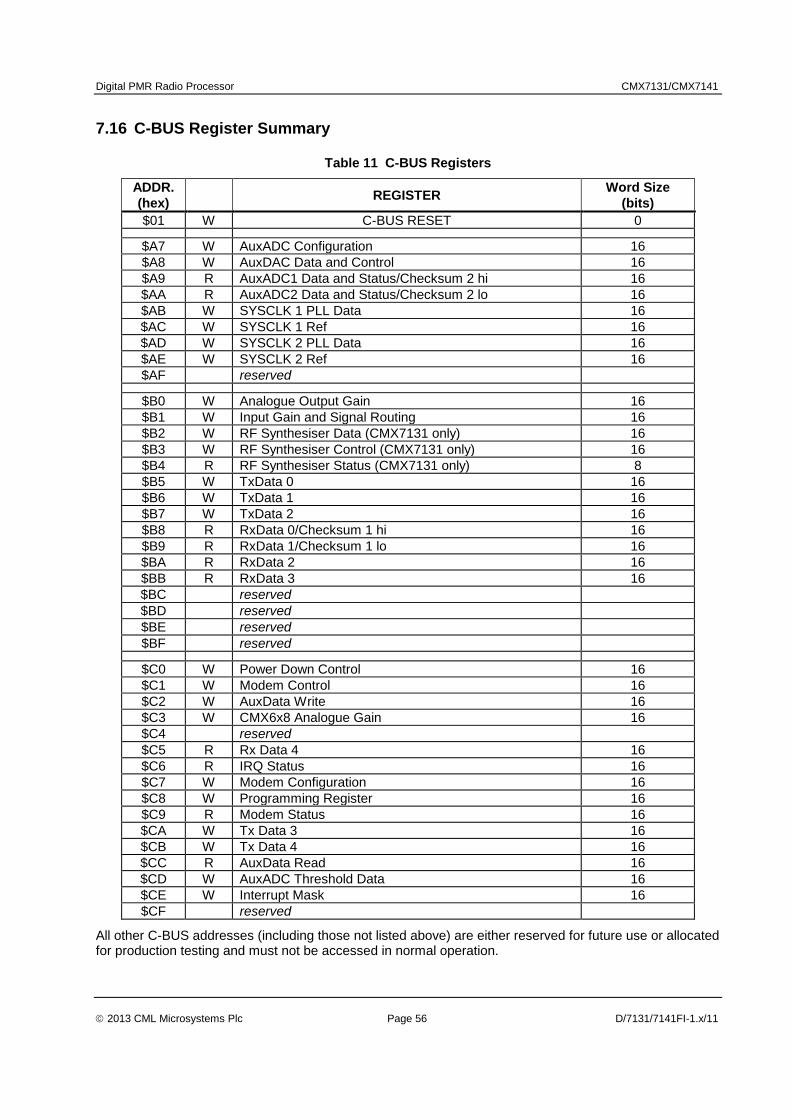
Digital PMR Radio Processor CMX7131/CMX7141
2013 CML Microsystems Plc Page 56 D/7131/7141FI-1.x/11
7.16 C-BUS Register Summary
Table 11 C-BUS Registers
ADDR.
(hex) REGISTER
Word Size
(bits)
$01 W C-BUS RESET 0
$A7 W AuxADC Configuration 16
$A8 W AuxDAC Data and Control 16
$A9 R AuxADC1 Data and Status/Checksum 2 hi 16
$AA R AuxADC2 Data and Status/Checksum 2 lo 16
$AB W SYSCLK 1 PLL Data 16
$AC W SYSCLK 1 Ref 16
$AD W SYSCLK 2 PLL Data 16
$AE W SYSCLK 2 Ref 16
$AF reserved
$B0 W Analogue Output Gain 16
$B1 W Input Gain and Signal Routing 16
$B2 W RF Synthesiser Data (CMX7131 only) 16
$B3 W RF Synthesiser Control (CMX7131 only) 16
$B4 R RF Synthesiser Status (CMX7131 only) 8
$B5 W TxData 0 16
$B6 W TxData 1 16
$B7 W TxData 2 16
$B8 R RxData 0/Checksum 1 hi 16
$B9 R RxData 1/Checksum 1 lo 16
$BA R RxData 2 16
$BB R RxData 3 16
$BC reserved
$BD reserved
$BE reserved
$BF reserved
$C0 W Power Down Control 16
$C1 W Modem Control 16
$C2 W AuxData Write 16
$C3 W CMX6x8 Analogue Gain 16
$C4 reserved
$C5 R Rx Data 4 16
$C6 R IRQ Status 16
$C7 W Modem Configuration 16
$C8 W Programming Register 16
$C9 R Modem Status 16
$CA W Tx Data 3 16
$CB W Tx Data 4 16
$CC R AuxData Read 16
$CD W AuxADC Threshold Data 16
$CE W Interrupt Mask 16
$CF reserved
All other C-BUS addresses (including those not listed above) are either reserved for future use or allocated for production testing and must not be accessed in normal operation.

Digital PMR Radio Processor CMX7131/CMX7141
2013 CML Microsystems Plc Page 57 D/7131/7141FI-1.x/11
8 Performance Specification
8.1 Electrical Performance
8.1.1 Absolute Maximum Ratings Exceeding these maximum ratings can result in damage to the device.
Min. Max. Unit
Supply: DVDD- DVSS 0.3 4.5 V
AVDD- AVSS 0.3 4.5 V
RFVDD- RFVSS (CMX7131 only) 0.3 4.5 V
CPVDD- RFVSS (CMX7131 only) 0.3 4.5 V
Voltage on any pin to DVSS 0.3 DVDD + 0.3 V
Voltage on any pin to AVSS 0.3 AVDD + 0.3 V
Current into or out of any power supply pin (excluding BIAS) (i.e.VDEC, AVDD, AVSS, DVDD, DVSS, CPVDD, RFVDDorRFVSS)
30 +30 mA
Current into or out of any other pin 20 +20 mA
Voltage differential between power supplies: DVDD and AVDD or CPVDD 0 0.3 V AVDD and CPVDD (CMX7131 only) 0 0.3 V DVSS and AVSS or RFVSS(CMX7131) 0 50 mV AVSS and RFVSS (CMX7131 only) 0 50 mV
L4 Package (48-pin LQFP) Min. Max. Unit
Total Allowable Power Dissipation at TAMB = 25°C – 1600 mW ... Derating – 16 mW/°C
Storage Temperature 55 +125 °C
Operating Temperature 40 +85 °C
Q3 Package (48-pin VQFN) Min. Max. Unit
Total Allowable Power Dissipation at TAMB = 25°C – 1750 mW ... Derating – 17.5 mW/°C
Storage Temperature 55 +125 °C
Operating Temperature 40 +85 °C
L9 Package (64-pin LQFP) Min. Max. Unit
Total Allowable Power Dissipation at TAMB = 25°C – 1690 mW … Derating – 16.9 mW/°C
Storage Temperature 55 +125 °C
Operating Temperature 40 +85 °C
Q1 Package (64-pin VQFN) Min. Max. Unit
Total Allowable Power Dissipation at TAMB = 25°C – 3500 mW … Derating – 35.0 mW/°C
Storage Temperature 55 +125 °C
Operating Temperature 40 +85 °C
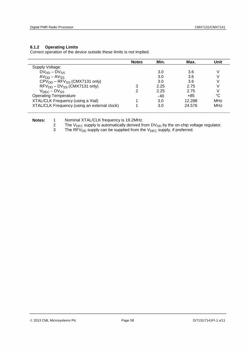
Digital PMR Radio Processor CMX7131/CMX7141
2013 CML Microsystems Plc Page 58 D/7131/7141FI-1.x/11
8.1.2 Operating Limits Correct operation of the device outside these limits is not implied.
Notes Min. Max. Unit
Supply Voltage: DVDD – DVSS 3.0 3.6 V AVDD – AVSS 3.0 3.6 V CPVDD – RFVSS (CMX7131 only) 3.0 3.6 V RFVDD – DVSS (CMX7131 only) 3 2.25 2.75 V VDEC – DVSS 2 2.25 2.75 V Operating Temperature 40 +85 °C
XTAL/CLK Frequency (using a Xtal) 1 3.0 12.288 MHz XTAL/CLK Frequency (using an external clock) 1 3.0 24.576 MHz
Notes: 1 Nominal XTAL/CLK frequency is 19.2MHz.
2 The VDEC supply is automatically derived from DVDD by the on-chip voltage regulator. 3 The RFVDD supply can be supplied from the VDEC supply, if preferred.
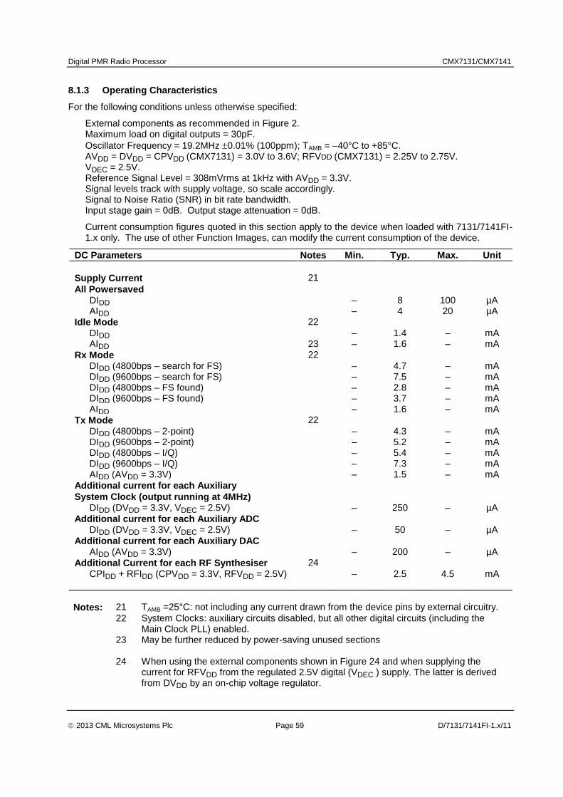
Digital PMR Radio Processor CMX7131/CMX7141
2013 CML Microsystems Plc Page 59 D/7131/7141FI-1.x/11
8.1.3 Operating Characteristics
For the following conditions unless otherwise specified:
External components as recommended in Figure 2. Maximum load on digital outputs = 30pF.
Oscillator Frequency = 19.2MHz 0.01% (100ppm); TAMB = 40°C to +85°C. AVDD = DVDD = CPVDD (CMX7131) = 3.0V to 3.6V; RFVDD (CMX7131) = 2.25V to 2.75V. VDEC = 2.5V. Reference Signal Level = 308mVrms at 1kHz with AVDD = 3.3V. Signal levels track with supply voltage, so scale accordingly. Signal to Noise Ratio (SNR) in bit rate bandwidth. Input stage gain = 0dB. Output stage attenuation = 0dB.
Current consumption figures quoted in this section apply to the device when loaded with 7131/7141FI-1.x only. The use of other Function Images, can modify the current consumption of the device.
DC Parameters Notes Min. Typ. Max. Unit
Supply Current 21
All Powersaved
DIDD – 8 100 µA AIDD – 4 20 µA
Idle Mode 22
DIDD – 1.4 – mA AIDD 23 – 1.6 – mA
Rx Mode 22
DIDD (4800bps – search for FS) – 4.7 – mA DIDD (9600bps – search for FS) – 7.5 – mA DIDD (4800bps – FS found) – 2.8 – mA DIDD (9600bps – FS found) – 3.7 – mA AIDD – 1.6 – mA
Tx Mode 22
DIDD (4800bps – 2-point) – 4.3 – mA DIDD (9600bps – 2-point) – 5.2 – mA DIDD (4800bps – I/Q) – 5.4 – mA DIDD (9600bps – I/Q) – 7.3 – mA AIDD (AVDD = 3.3V) – 1.5 – mA
Additional current for each Auxiliary
System Clock (output running at 4MHz)
DIDD (DVDD = 3.3V, VDEC = 2.5V) – 250 – µA
Additional current for each Auxiliary ADC
DIDD (DVDD = 3.3V, VDEC = 2.5V) – 50 – µA
Additional current for each Auxiliary DAC
AIDD (AVDD = 3.3V) – 200 – µA
Additional Current for each RF Synthesiser 24
CPIDD + RFIDD (CPVDD = 3.3V, RFVDD = 2.5V) – 2.5 4.5 mA
Notes: 21 TAMB =25°C: not including any current drawn from the device pins by external circuitry.
22 System Clocks: auxiliary circuits disabled, but all other digital circuits (including the Main Clock PLL) enabled.
23 May be further reduced by power-saving unused sections
24 When using the external components shown in Figure 24 and when supplying the current for RFVDD from the regulated 2.5V digital (VDEC ) supply. The latter is derived from DVDD by an on-chip voltage regulator.
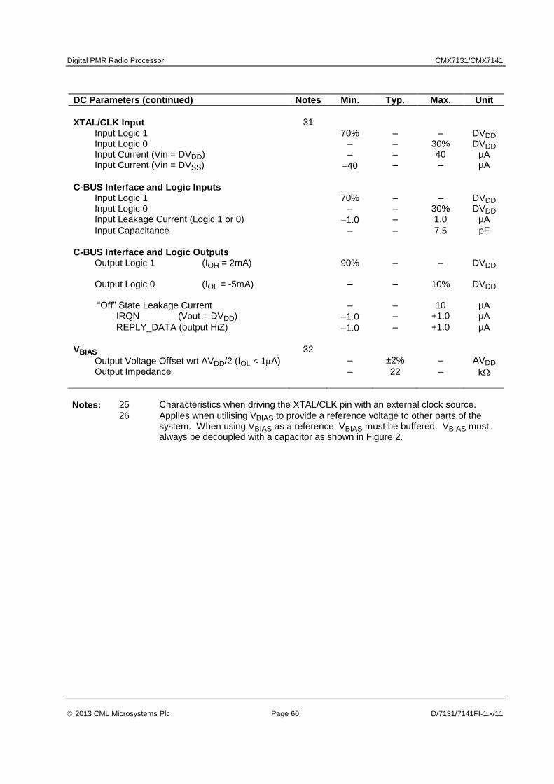
Digital PMR Radio Processor CMX7131/CMX7141
2013 CML Microsystems Plc Page 60 D/7131/7141FI-1.x/11
DC Parameters (continued) Notes Min. Typ. Max. Unit
XTAL/CLK Input 31
Input Logic 1 70% – – DVDD Input Logic 0 – – 30% DVDD Input Current (Vin = DVDD) – – 40 µA Input Current (Vin = DVSS) 40 – – µA
C-BUS Interface and Logic Inputs
Input Logic 1 70% – – DVDD Input Logic 0 – – 30% DVDD Input Leakage Current (Logic 1 or 0) 1.0 – 1.0 µA
Input Capacitance – – 7.5 pF
C-BUS Interface and Logic Outputs
Output Logic 1 (IOH = 2mA) 90% – – DVDD Output Logic 0 (IOL = -5mA) – – 10% DVDD “Off” State Leakage Current – – 10 µA
IRQN (Vout = DVDD) 1.0 – +1.0 µA
REPLY_DATA (output HiZ) 1.0 – +1.0 µA
VBIAS 32
Output Voltage Offset wrt AVDD/2 (IOL < 1A) – ±2% – AVDD
Output Impedance – 22 – k
Notes: 25 Characteristics when driving the XTAL/CLK pin with an external clock source.
26 Applies when utilising VBIAS to provide a reference voltage to other parts of the system. When using VBIAS as a reference, VBIAS must be buffered. VBIAS must always be decoupled with a capacitor as shown in Figure 2.

Digital PMR Radio Processor CMX7131/CMX7141
2013 CML Microsystems Plc Page 61 D/7131/7141FI-1.x/11
AC Parameters Notes Min. Typ. Max. Unit
XTAL/CLK Input
'High' Pulse Width 31 15 – – ns 'Low' Pulse Width 31 15 – – ns Input Impedance (at 6.144MHz)
Powered-up Resistance – 150 – k Capacitance – 20 – pF Powered-down Resistance – 300 – k Capacitance – 20 – pF
Xtal Start-up Time (from powersave) – 20 – ms
System Clk 1/2 Outputs
XTAL/CLK input to CLOCK_OUT timing: (in high to out high) 32 – 15 – ns (in low to out low) 32 – 15 – ns 'High' Pulse Width 33 76 81.38 87 ns 'Low' Pulse Width 33 76 81.38 87 ns
VBIAS
Start-up Time (from powersave) – 30 – ms
Microphone, Alternative and Discriminator
Inputs (MIC, ALT, DISC)
Input Impedance 34 – >10 – M Maximum Input Level (pk-pk) 35 – – 80% AVDD Load Resistance (feedback pins) 80 – – k Amplifier Open Loop Voltage Gain
(I/P = 1mVrms at 100Hz) – 80 – dB
Unity Gain Bandwidth – 1.0 – MHz
Programmable Input Gain Stage 36
Gain (at 0dB) 37 0.5 0 +0.5 dB
Cumulative Gain Error
(wrt attenuation at 0dB) 37 1.0 0 +1.0 dB
Notes: 31 Timing for an external input to the XTAL/CLK pin.
32 XTAL/CLK input driven by an external source. 33 6.144MHz XTAL fitted and 6.144MHz output selected (scale for 19.2MHz). 34 With no external components connected, measured at DC. 35 Centered about AVDD/2; after multiplying by the gain of input circuit (with external
components connected). 36 Gain applied to signal at output of buffer amplifier: DISCFB, ALTFB or MICFB 37 Design Value. Overall attenuation input to output has a tolerance of 0dB ±1.0dB
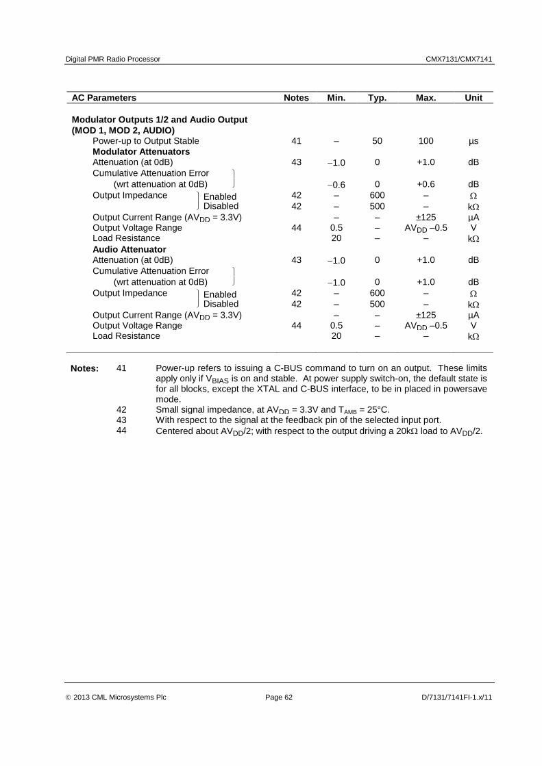
Digital PMR Radio Processor CMX7131/CMX7141
2013 CML Microsystems Plc Page 62 D/7131/7141FI-1.x/11
AC Parameters Notes Min. Typ. Max. Unit
Modulator Outputs 1/2 and Audio Output
(MOD 1, MOD 2, AUDIO)
Power-up to Output Stable 41 – 50 100 µs
Modulator Attenuators
Attenuation (at 0dB) 43 1.0 0 +1.0 dB
Cumulative Attenuation Error
(wrt attenuation at 0dB) 0.6 0 +0.6 dB
Output Impedance Enabled 42 – 600 – Disabled 42 – 500 – k Output Current Range (AVDD = 3.3V) – – ±125 µA Output Voltage Range 44 0.5 – AVDD –0.5 V Load Resistance 20 – – k
Audio Attenuator
Attenuation (at 0dB) 43 1.0 0 +1.0 dB
Cumulative Attenuation Error
(wrt attenuation at 0dB) 1.0 0 +1.0 dB
Output Impedance Enabled 42 – 600 – Disabled 42 – 500 – k Output Current Range (AVDD = 3.3V) – – ±125 µA Output Voltage Range 44 0.5 – AVDD –0.5 V Load Resistance 20 – – k
Notes: 41 Power-up refers to issuing a C-BUS command to turn on an output. These limits apply only if VBIAS is on and stable. At power supply switch-on, the default state is for all blocks, except the XTAL and C-BUS interface, to be in placed in powersave mode.
42 Small signal impedance, at AVDD = 3.3V and TAMB = 25°C. 43 With respect to the signal at the feedback pin of the selected input port. 44 Centered about AVDD/2; with respect to the output driving a 20k load to AVDD/2.

Digital PMR Radio Processor CMX7131/CMX7141
2013 CML Microsystems Plc Page 63 D/7131/7141FI-1.x/11
AC Parameters (cont.) Notes Min. Typ. Max. Unit
Auxiliary Signal Inputs (Aux ADC 1 to 4)
Source Output Impedance 51 – – 24 k
Auxiliary 10 Bit ADCs
Resolution – 10 – Bits Maximum Input Level (pk-pk) 54 – – 80% AVDD Conversion Time 52 – 250 – µs Input Impedance
Resistance 57 – >10 – M Capacitance – 5 – pF
Zero Error 55 0 – ±10 mV Integral Non-linearity – – ±3 LSBs Differential Non-linearity 53 – – ±1 LSBs
Auxiliary 10 Bit DACs
Resolution – 10 – Bits Maximum Output Level (pk-pk), no load 54 80% – – AVDD Zero Error 56 0 – ±10 mV Resistive Load 5 – – k Integral Non-linearity – – ±4 LSBs Differential Non-linearity 53 – – ±1 LSBs
Notes: 51 Denotes output impedance of the driver of the auxiliary input signal, to ensure < 1 bit additional error under nominal conditions.
52 With an auxiliary clock frequency of 6.144MHz. 53 Guaranteed monotonic with no missing codes. 54 Centred about AVDD/2. 55 Input offset from a nominal VBIAS input, which produces a $0200 ADC output. 56 Output offset from a $0200 DAC input, measured wrt a nominal VBIAS output. 57 Measured at dc.
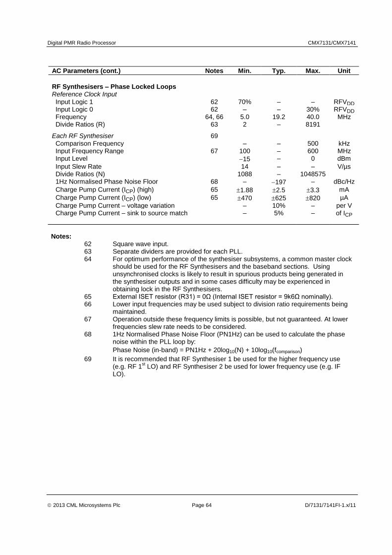
Digital PMR Radio Processor CMX7131/CMX7141
2013 CML Microsystems Plc Page 64 D/7131/7141FI-1.x/11
AC Parameters (cont.) Notes Min. Typ. Max. Unit
RF Synthesisers – Phase Locked Loops
Reference Clock Input Input Logic 1 62 70% – – RFVDD Input Logic 0 62 – – 30% RFVDD Frequency 64, 66 5.0 19.2 40.0 MHz Divide Ratios (R) 63 2 – 8191
Each RF Synthesiser 69 Comparison Frequency – – 500 kHz Input Frequency Range 67 100 – 600 MHz Input Level 15 – 0 dBm
Input Slew Rate 14 – – V/µs Divide Ratios (N) 1088 – 1048575 1Hz Normalised Phase Noise Floor 68 – 197 – dBc/Hz
Charge Pump Current (ICP) (high) 65 1.88 2.5 3.3 mA
Charge Pump Current (ICP) (low) 65 470 625 820 µA
Charge Pump Current – voltage variation – 10% – per V Charge Pump Current – sink to source match – 5% – of ICP
Notes:
62 Square wave input. 63 Separate dividers are provided for each PLL. 64 For optimum performance of the synthesiser subsystems, a common master clock
should be used for the RF Synthesisers and the baseband sections. Using unsynchronised clocks is likely to result in spurious products being generated in the synthesiser outputs and in some cases difficulty may be experienced in obtaining lock in the RF Synthesisers.
65 External ISET resistor (R31) = 0Ω (Internal ISET resistor = 9k6Ω nominally). 66 Lower input frequencies may be used subject to division ratio requirements being
maintained. 67 Operation outside these frequency limits is possible, but not guaranteed. At lower
frequencies slew rate needs to be considered. 68 1Hz Normalised Phase Noise Floor (PN1Hz) can be used to calculate the phase
noise within the PLL loop by:
Phase Noise (in-band) = PN1Hz + 20log10(N) + 10log10(fcomparison)
69 It is recommended that RF Synthesiser 1 be used for the higher frequency use (e.g. RF 1
st LO) and RF Synthesiser 2 be used for lower frequency use (e.g. IF
LO).
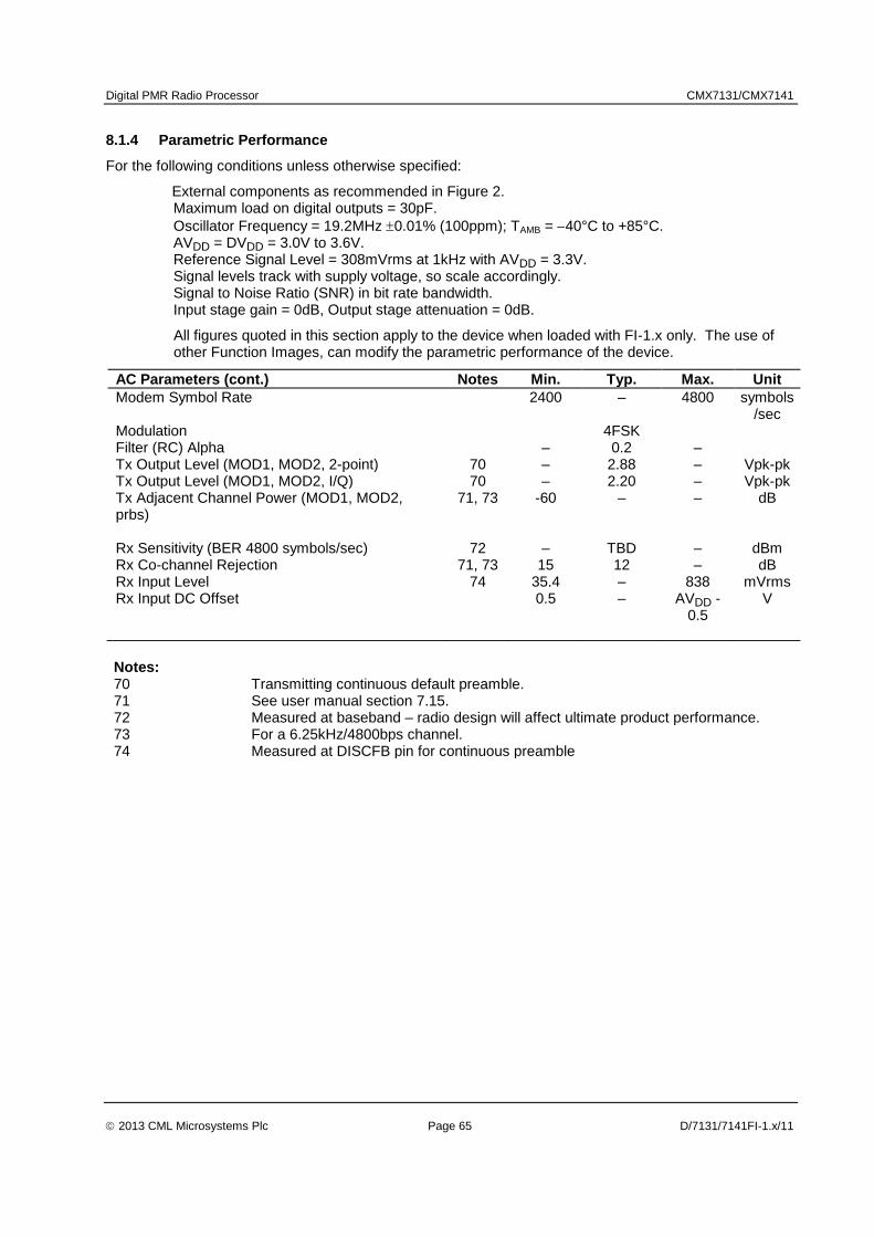
Digital PMR Radio Processor CMX7131/CMX7141
2013 CML Microsystems Plc Page 65 D/7131/7141FI-1.x/11
8.1.4 Parametric Performance
For the following conditions unless otherwise specified:
External components as recommended in Figure 2. Maximum load on digital outputs = 30pF.
Oscillator Frequency = 19.2MHz 0.01% (100ppm); TAMB = 40°C to +85°C. AVDD = DVDD = 3.0V to 3.6V. Reference Signal Level = 308mVrms at 1kHz with AVDD = 3.3V. Signal levels track with supply voltage, so scale accordingly. Signal to Noise Ratio (SNR) in bit rate bandwidth. Input stage gain = 0dB, Output stage attenuation = 0dB.
All figures quoted in this section apply to the device when loaded with FI-1.x only. The use of other Function Images, can modify the parametric performance of the device.
AC Parameters (cont.) Notes Min. Typ. Max. Unit
Modem Symbol Rate 2400 – 4800 symbols /sec
Modulation 4FSK Filter (RC) Alpha – 0.2 – Tx Output Level (MOD1, MOD2, 2-point) 70 – 2.88 – Vpk-pk Tx Output Level (MOD1, MOD2, I/Q) 70 – 2.20 – Vpk-pk Tx Adjacent Channel Power (MOD1, MOD2, prbs)
71, 73 -60 – – dB
Rx Sensitivity (BER 4800 symbols/sec) 72 – TBD – dBm Rx Co-channel Rejection 71, 73 15 12 – dB Rx Input Level 74 35.4 – 838 mVrms Rx Input DC Offset 0.5 – AVDD -
0.5 V
Notes:
70 Transmitting continuous default preamble. 71 See user manual section 7.15. 72 Measured at baseband – radio design will affect ultimate product performance. 73 For a 6.25kHz/4800bps channel. 74 Measured at DISCFB pin for continuous preamble
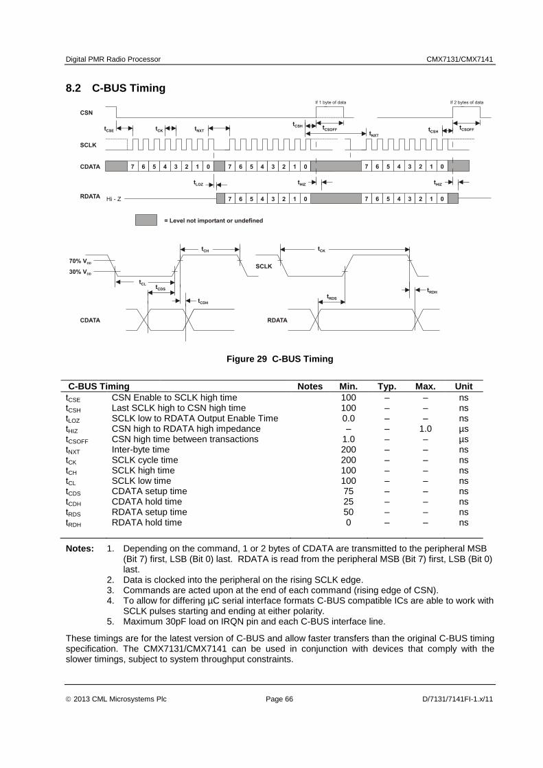
Digital PMR Radio Processor CMX7131/CMX7141
2013 CML Microsystems Plc Page 66 D/7131/7141FI-1.x/11
8.2 C-BUS Timing
Figure 29 C-BUS Timing
C-BUS Timing Notes Min. Typ. Max. Unit
tCSE CSN Enable to SCLK high time 100 – – ns tCSH Last SCLK high to CSN high time 100 – – ns tLOZ SCLK low to RDATA Output Enable Time 0.0 – – ns tHIZ CSN high to RDATA high impedance – – 1.0 µs tCSOFF CSN high time between transactions 1.0 – – µs tNXT Inter-byte time 200 – – ns tCK SCLK cycle time 200 – – ns tCH SCLK high time 100 – – ns tCL SCLK low time 100 – – ns tCDS CDATA setup time 75 – – ns tCDH CDATA hold time 25 – – ns tRDS RDATA setup time 50 – – ns tRDH RDATA hold time 0 – – ns
Notes: 1. Depending on the command, 1 or 2 bytes of CDATA are transmitted to the peripheral MSB (Bit 7) first, LSB (Bit 0) last. RDATA is read from the peripheral MSB (Bit 7) first, LSB (Bit 0) last.
2. Data is clocked into the peripheral on the rising SCLK edge. 3. Commands are acted upon at the end of each command (rising edge of CSN). 4. To allow for differing µC serial interface formats C-BUS compatible ICs are able to work with
SCLK pulses starting and ending at either polarity. 5. Maximum 30pF load on IRQN pin and each C-BUS interface line.
These timings are for the latest version of C-BUS and allow faster transfers than the original C-BUS timing specification. The CMX7131/CMX7141 can be used in conjunction with devices that comply with the slower timings, subject to system throughput constraints.
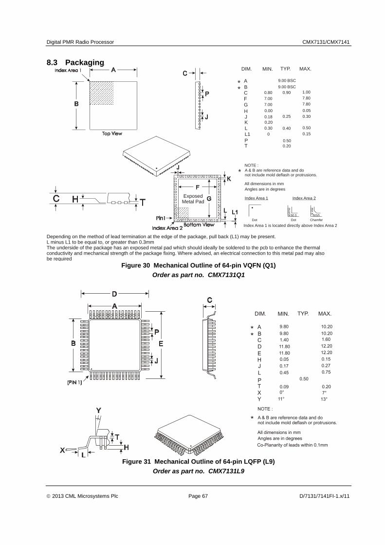
Digital PMR Radio Processor CMX7131/CMX7141
2013 CML Microsystems Plc Page 67 D/7131/7141FI-1.x/11
8.3 Packaging
A
BC
H
TYP. MAX.MIN.DIM.
J
PT
1.000.80
0.05
0.30
0.50
0.00
0.20
0.18
9.00 BSC
9.00 BSC**
NOTE :
*
All dimensions in mm
Angles are in degrees
A & B are reference data and donot include mold deflash or protrusions.
F 7.807.00
G 7.807.00
L 0.500.30
Index Area 1
Dot
Index Area 2
Dot Chamfer
Index Area 1 is located directly above Index Area 2
Depending on the method of lead termination at the edge of the package, pull back (L1) may be present. L minus L1 to be equal to, or greater than 0.3mmThe underside of the package has an exposed metal pad which should ideally be soldered to the pcb to enhance the thermal conductivity and mechanical strength of the package fixing. Where advised, an electrical connection to this metal pad may also be required
L1 0.150
K 0.20
0.90
0.25
0.40
ExposedMetal Pad
Figure 30 Mechanical Outline of 64-pin VQFN (Q1)
Order as part no. CMX7131Q1
Figure 31 Mechanical Outline of 64-pin LQFP (L9)
Order as part no. CMX7131L9
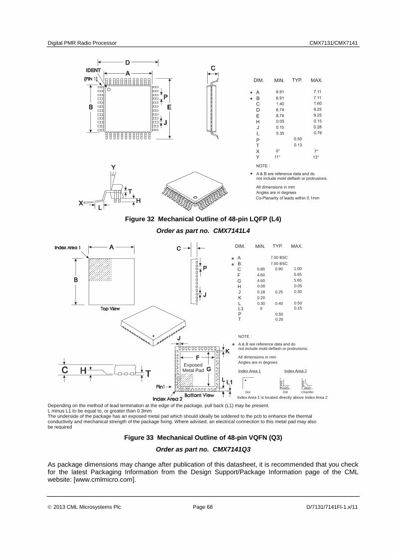
Digital PMR Radio Processor CMX7131/CMX7141
2013 CML Microsystems Plc Page 68 D/7131/7141FI-1.x/11
Figure 32 Mechanical Outline of 48-pin LQFP (L4)
Order as part no. CMX7141L4
Depending on the method of lead termination at the edge of the package, pull back (L1) may be present. L minus L1 to be equal to, or greater than 0.3mmThe underside of the package has an exposed metal pad which should ideally be soldered to the pcb to enhance the thermal conductivity and mechanical strength of the package fixing. Where advised, an electrical connection to this metal pad may also be required
A
BC
H
TYP. MAX.MIN.DIM.
J
1.000.80
0.05
0.30
0.00
0.18
7.00 BSC
7.00 BSC**
NOTE :
*
All dimensions in mm
Angles are in degrees
A & B are reference data and donot include mold deflash or protrusions.
F 5.654.60
G 5.654.60
L 0.500.30
Index Area 1
Dot
Index Area 2
Dot Chamfer
Index Area 1 is located directly above Index Area 2
PT
0.50
0.20
L1 0.150
ExposedMetal Pad
K 0.20
0.90
0.25
0.40
Figure 33 Mechanical Outline of 48-pin VQFN (Q3)
Order as part no. CMX7141Q3 As package dimensions may change after publication of this datasheet, it is recommended that you check for the latest Packaging Information from the Design Support/Package Information page of the CML website: [www.cmlmicro.com].

Digital PMR Radio Processor CMX7131/CMX7141
2013 CML Microsystems Plc Page 69 D/7131/7141FI-1.x/11
About FirmASIC
CML’s proprietary FirmASIC component technology reduces cost, time to market and development risk,
with increased flexibility for the designer and end application. FirmASIC combines Analogue, Digital, Firmware and Memory technologies in a single silicon platform that can be focused to deliver the right
feature mix, performance and price for a target application family. Specific functions of a FirmASIC device are determined by uploading its Function Image™ during device initialization. New Function Images™ may be later provided to supplement and enhance device functions, expanding or modifying end-product features without the need for expensive and time-consuming design changes.
FirmASIC devices provide significant time to market and commercial benefits over Custom ASIC, Structured ASIC, FPGA and DSP solutions. They may also be exclusively customised where security or intellectual property issues prevent the use of Application Specific Standard Products (ASSP’s).
Handling precautions: This product includes input protection, however, precautions should be taken to prevent device damage from electro-static discharge. CML does not assume any responsibility for the use of any circuitry described. No IPR or circuit patent licences are implied. CML reserves the right at any time without notice to change the said circuitry and this product specification. CML has a policy of testing every product shipped using calibrated test equipment to ensure compliance with this product specification. Specific testing of all circuit parameters is not necessarily performed.


