Digital Phase-Locked Loop (Rev. D) - Texas Instruments DIGITAL PHASE-LOCKED LOOP SCHS297D – AUGUST...
18
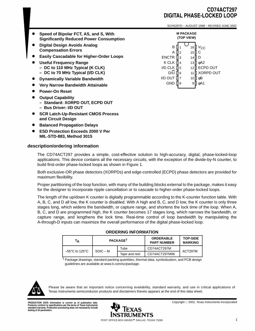
CD74ACT297 DIGITAL PHASE-LOCKED LOOP SCHS297D – AUGUST 1998 – REVISED JUNE 2002 1 POST OFFICE BOX 655303 • DALLAS, TEXAS 75265 Speed of Bipolar FCT, AS, and S, With Significantly Reduced Power Consumption Digital Design Avoids Analog Compensation Errors Easily Cascadable for Higher-Order Loops Useful Frequency Range – DC to 110 MHz Typical (K CLK) – DC to 70 MHz Typical (I/D CLK) Dynamically Variable Bandwidth Very Narrow Bandwidth Attainable Power-On Reset Output Capability – Standard: XORPD OUT, ECPD OUT – Bus Driver: I/D OUT SCR Latch-Up-Resistant CMOS Process and Circuit Design Balanced Propagation Delays ESD Protection Exceeds 2000 V Per MIL-STD-883, Method 3015 description/ordering information The CD74ACT297 provides a simple, cost-effective solution to high-accuracy, digital, phase-locked-loop applications. This device contains all the necessary circuits, with the exception of the divide-by-N counter, to build first-order phase-locked loops as shown in Figure 1. Both exclusive-OR phase detectors (XORPDs) and edge-controlled (ECPD) phase detectors are provided for maximum flexibility. Proper partitioning of the loop function, with many of the building blocks external to the package, makes it easy for the designer to incorporate ripple cancellation or to cascade to higher-order phase-locked loops. The length of the up/down K counter is digitally programmable according to the K-counter function table. With A, B, C, and D all low, the K counter is disabled. With A high and B, C, and D low, the K counter is only three stages long, which widens the bandwidth, or capture range, and shortens the lock time of the loop. When A, B, C, and D are programmed high, the K counter becomes 17 stages long, which narrows the bandwidth, or capture range, and lengthens the lock time. Real-time control of loop bandwidth by manipulating the A-through-D inputs can maximize the overall performance of the digital phase-locked loop. ORDERING INFORMATION T A PACKAGE † ORDERABLE PART NUMBER TOP-SIDE MARKING 55°C to 125°C SOIC M Tube CD74ACT297M ACT297M –55°C to 125°C SOIC – M Tape and reel CD74ACT297M96 ACT297M † Package drawings, standard packing quantities, thermal data, symbolization, and PCB design guidelines are available at www.ti.com/sc/package. Copyright 2002, Texas Instruments Incorporated PRODUCTION DATA information is current as of publication date. Products conform to specifications per the terms of Texas Instruments standard warranty. Production processing does not necessarily include testing of all parameters. Please be aware that an important notice concerning availability, standard warranty, and use in critical applications of Texas Instruments semiconductor products and disclaimers thereto appears at the end of this data sheet. 1 2 3 4 5 6 7 8 16 15 14 13 12 11 10 9 B A ENCTR K CLK I/D CLK D/U I/D OUT GND V CC C D φA2 ECPD OUT XORPD OUT φB φA1 M PACKAGE (TOP VIEW)
Transcript of Digital Phase-Locked Loop (Rev. D) - Texas Instruments DIGITAL PHASE-LOCKED LOOP SCHS297D – AUGUST...
CD74ACT297DIGITAL PHASE-LOCKED LOOP
SCHS297D – AUGUST 1998 – REVISED JUNE 2002
1POST OFFICE BOX 655303 • DALLAS, TEXAS 75265
Speed of Bipolar FCT, AS, and S, WithSignificantly Reduced Power Consumption
Digital Design Avoids AnalogCompensation Errors
Easily Cascadable for Higher-Order Loops
Useful Frequency Range– DC to 110 MHz Typical (K CLK)– DC to 70 MHz Typical (I/D CLK)
Dynamically Variable Bandwidth
Very Narrow Bandwidth Attainable
Power-On Reset
Output Capability– Standard: XORPD OUT, ECPD OUT– Bus Driver: I/D OUT
SCR Latch-Up-Resistant CMOS Processand Circuit Design
Balanced Propagation Delays
ESD Protection Exceeds 2000 V PerMIL-STD-883, Method 3015
description/ordering information
The CD74ACT297 provides a simple, cost-effective solution to high-accuracy, digital, phase-locked-loopapplications. This device contains all the necessary circuits, with the exception of the divide-by-N counter, tobuild first-order phase-locked loops as shown in Figure 1.
Both exclusive-OR phase detectors (XORPDs) and edge-controlled (ECPD) phase detectors are provided formaximum flexibility.
Proper partitioning of the loop function, with many of the building blocks external to the package, makes it easyfor the designer to incorporate ripple cancellation or to cascade to higher-order phase-locked loops.
The length of the up/down K counter is digitally programmable according to the K-counter function table. WithA, B, C, and D all low, the K counter is disabled. With A high and B, C, and D low, the K counter is only threestages long, which widens the bandwidth, or capture range, and shortens the lock time of the loop. When A,B, C, and D are programmed high, the K counter becomes 17 stages long, which narrows the bandwidth, orcapture range, and lengthens the lock time. Real-time control of loop bandwidth by manipulating theA-through-D inputs can maximize the overall performance of the digital phase-locked loop.
ORDERING INFORMATION
TA PACKAGE† ORDERABLEPART NUMBER
TOP-SIDEMARKING
55°C to 125°C SOIC MTube CD74ACT297M
ACT297M–55°C to 125°C SOIC – MTape and reel CD74ACT297M96
ACT297M
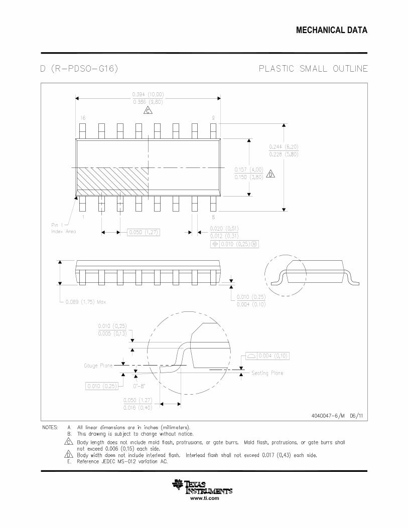
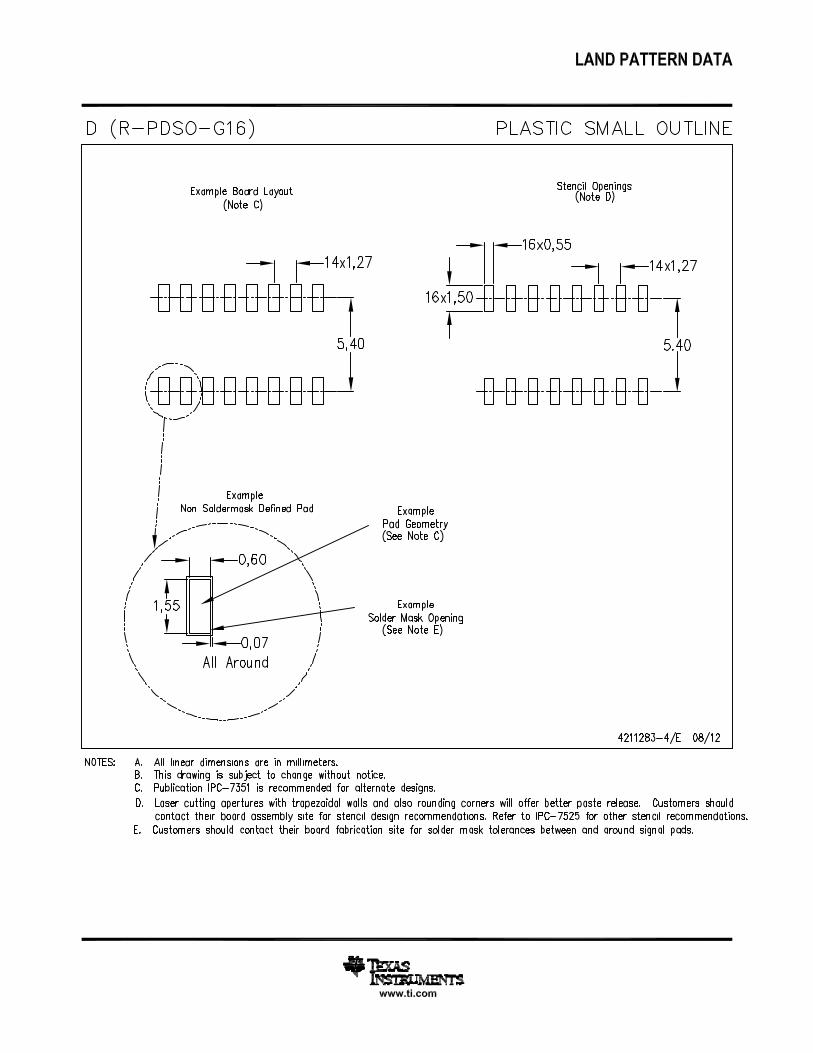
† Package drawings, standard packing quantities, thermal data, symbolization, and PCB designguidelines are available at www.ti.com/sc/package.
Copyright 2002, Texas Instruments IncorporatedPRODUCTION DATA information is current as of publication date.Products conform to specifications per the terms of Texas Instrumentsstandard warranty. Production processing does not necessarily includetesting of all parameters.
Please be aware that an important notice concerning availability, standard warranty, and use in critical applications ofTexas Instruments semiconductor products and disclaimers thereto appears at the end of this data sheet.
1
2
3
4
5
6
7
8
16
15
14
13
12
11
10
9
BA
ENCTRK CLK
I/D CLKD/U
I/D OUTGND
VCCCDφA2ECPD OUTXORPD OUTφBφA1
M PACKAGE(TOP VIEW)
CD74ACT297DIGITAL PHASE-LOCKED LOOP
SCHS297D – AUGUST 1998 – REVISED JUNE 2002
2 POST OFFICE BOX 655303 • DALLAS, TEXAS 75265
description/ordering information (continued)
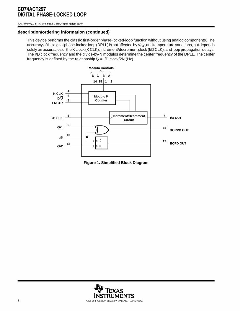
This device performs the classic first-order phase-locked-loop function without using analog components. Theaccuracy of the digital phase-locked loop (DPLL) is not affected by VCC and temperature variations, but dependssolely on accuracies of the K clock (K CLK), increment/decrement clock (I/D CLK), and loop propagation delays.The I/D clock frequency and the divide-by-N modulos determine the center frequency of the DPLL. The centerfrequency is defined by the relationship fc = I/D clock/2N (Hz).
Increment/DecrementCircuit
Modulo KCounter
K CLK
I/D CLK
φB
φA2
D/UENCTR
φA1
D C B A
14 15 1 2
4
63
5
9
10
13
7
11
12J
KECPD OUT
XORPD OUT
I/D OUT
Modulo Controls
Figure 1. Simplified Block Diagram
CD74ACT297DIGITAL PHASE-LOCKED LOOP
SCHS297D – AUGUST 1998 – REVISED JUNE 2002
3POST OFFICE BOX 655303 • DALLAS, TEXAS 75265
Function Tables
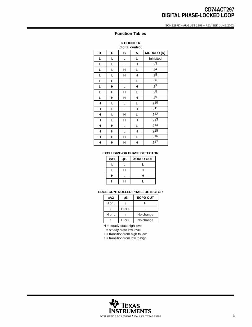
K COUNTER(digital control)
D C B A MODULO (K)
L L L L Inhibited
L L L H 23
L L H L 24
L L H H 25
L H L L 26
L H L H 27
L H H L 28
L H H H 29
H L L L 210
H L L H 211
H L H L 212
H L H H 213
H H L L 214
H H L H 215
H H H L 216
H H H H 217
EXCLUSIVE-OR PHASE DETECTOR
φA1 φB XORPD OUT
L L L
L H H
H L H
H H L
EDGE-CONTROLLED PHASE DETECTOR
φA2 φB ECPD OUT
H or L ↓ H
↓ H or L L
H or L ↑ No change
↑ H or L No change
H = steady-state high levelL = steady-state low level↓ = transition from high to low↑ = transition from low to high

CD74ACT297DIGITAL PHASE-LOCKED LOOP
SCHS297D – AUGUST 1998 – REVISED JUNE 2002
4 POST OFFICE BOX 655303 • DALLAS, TEXAS 75265
functional block diagram
D/U
To Mode Controls 12–2 (11 stages not shown)
2 1
15
1446 35
9
10
13
78910111213140
1248
2
1A
B
CD
4
6
3
5
K CLK
ENCTR
I/D CLK
I/D OUT
Power-Up Reset
l = 1
C20
20D
XORPD OUT
ECPD OUT
R14D
14T
M14
13D
M13
1T
Increment
RRRRR
T T T
1T T
13T
13T20D
C20
T T
14D
14T
M13
13DR R RR
M14
RR
I/D Circuit
Decrement
7
11
12
RR
S S
C21
C21 C21
C21 C21
C21
C21
C21
C21
21D 21D
21D
21D
21D
21D
21D21D
Exclusive-OR Phase Detector
Edge-Controlled Phase Detector
φA1
φB
φA2
1
X/Y
K Counter
21J
21K
CD74ACT297DIGITAL PHASE-LOCKED LOOP
SCHS297D – AUGUST 1998 – REVISED JUNE 2002
5POST OFFICE BOX 655303 • DALLAS, TEXAS 75265
detailed description
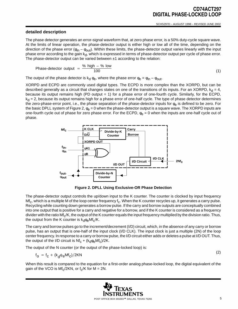
The phase detector generates an error-signal waveform that, at zero phase error, is a 50% duty-cycle square wave.At the limits of linear operation, the phase-detector output is either high or low all of the time, depending on thedirection of the phase error (φin – φout). Within these limits, the phase-detector output varies linearly with the inputphase error according to the gain kd, which is expressed in terms of phase-detector output per cycle of phase error.The phase-detector output can be varied between ±1 according to the relation:
Phase-detector output % high – % low
100
The output of the phase detector is kd φe, where the phase error φe = φin – φout.
XORPD and ECPD are commonly used digital types. The ECPD is more complex than the XORPD, but can bedescribed generally as a circuit that changes states on one of the transitions of its inputs. For an XORPD, kd = 4,because its output remains high (PD output = 1) for a phase error of one-fourth cycle. Similarly, for the ECPD,kd = 2, because its output remains high for a phase error of one-half cycle. The type of phase detector determinesthe zero-phase-error point, i.e., the phase separation of the phase-detector inputs for φe is defined to be zero. Forthe basic DPLL system of Figure 2, φe = 0 when the phase-detector output is a square wave. The XORPD inputs areone-fourth cycle out of phase for zero phase error. For the ECPD, φe = 0 when the inputs are one-half cycle out ofphase.
D/U
φB
φA1
Divide-by-NCounter
Divide-by-KCounter
fin,φin
Mfc
I/D CircuitI/D OUT
I/D CLK
Carry
Borrow
K CLK
XORPD OUT
fout,φout
2Nfc
Figure 2. DPLL Using Exclusive-OR Phase Detection
The phase-detector output controls the up/down input to the K counter. The counter is clocked by input frequencyMfc, which is a multiple M of the loop center frequency fc. When the K counter recycles up, it generates a carry pulse.Recycling while counting down generates a borrow pulse. If the carry and borrow outputs are conceptually combinedinto one output that is positive for a carry and negative for a borrow, and if the K counter is considered as a frequencydivider with the ratio Mfc/K, the output of the K counter equals the input frequency multiplied by the division ratio. Thus,the output from the K counter is kdφeMfc/K.
The carry and borrow pulses go to the increment/decrement (I/D) circuit, which, in the absence of any carry or borrowpulse, has an output that is one-half of the input clock (I/D CLK). The input clock is just a multiple (2N) of the loopcenter frequency. In response to a carry or borrow pulse, the I/D circuit either adds or deletes a pulse at I/D OUT. Thus,the output of the I/D circuit is Nfc + (kdφeMfc)/2K.
The output of the N counter (or the output of the phase-locked loop) is:
fo fc (kdeMfc)2KN
When this result is compared to the equation for a first-order analog phase-locked loop, the digital equivalent of thegain of the VCO is Mfc/2KN, or fc/K for M = 2N.
(1)
(2)
CD74ACT297DIGITAL PHASE-LOCKED LOOP
SCHS297D – AUGUST 1998 – REVISED JUNE 2002
6 POST OFFICE BOX 655303 • DALLAS, TEXAS 75265
detailed description (continued)
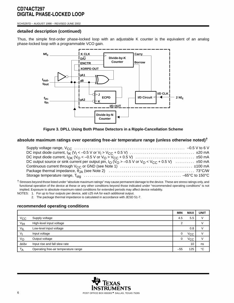
Thus, the simple first-order phase-locked loop with an adjustable K counter is the equivalent of an analogphase-locked loop with a programmable VCO gain.
D/U
φA2
Divide-by-KCounter
Divide-by-NCounter
Mfc
I/D Circuit
I/D OUT
I/D CLK
Carry
Borrow
K CLK
XORPD OUT
φB
fin,φin
2 Nfc
fout,φout
φA1
J
KECPD
ENCTR
Figure 3. DPLL Using Both Phase Detectors in a Ripple-Cancellation Scheme
absolute maximum ratings over operating free-air temperature range (unless otherwise noted)†
Supply voltage range, VCC –0.5 V to 6 V. . . . . . . . . . . . . . . . . . . . . . . . . . . . . . . . . . . . . . . . . . . . . . . . . . . . . . . . . . DC input diode current, IIK (VI < –0.5 V or VI > VCC + 0.5 V) ±20 mA. . . . . . . . . . . . . . . . . . . . . . . . . . . . . . . . . . DC input diode current, IOK (VO < –0.5 V or VO > VCC + 0.5 V) ±50 mA. . . . . . . . . . . . . . . . . . . . . . . . . . . . . . . DC output source or sink current per output pin, IO (VO > –0.5 V or VO < VCC + 0.5 V) ±50 mA. . . . . . . . . . Continuous current through VCC or GND (see Note 1) ±100 mA. . . . . . . . . . . . . . . . . . . . . . . . . . . . . . . . . . . . . . Package thermal impedance, θJA (see Note 2) 73°C/W. . . . . . . . . . . . . . . . . . . . . . . . . . . . . . . . . . . . . . . . . . . . . Storage temperature range, Tstg –65°C to 150°C. . . . . . . . . . . . . . . . . . . . . . . . . . . . . . . . . . . . . . . . . . . . . . . . . . .
† Stresses beyond those listed under “absolute maximum ratings” may cause permanent damage to the device. These are stress ratings only, andfunctional operation of the device at these or any other conditions beyond those indicated under “recommended operating conditions” is notimplied. Exposure to absolute-maximum-rated conditions for extended periods may affect device reliability.
NOTES: 1. For up to four outputs per device, add ±25 mA for each additional output.2. The package thermal impedance is calculated in accordance with JESD 51-7.
recommended operating conditions
MIN MAX UNIT
VCC Supply voltage 4.5 5.5 V
VIH High-level input voltage 2 V
VIL Low-level input voltage 0.8 V
VI Input voltage 0 VCC V
VO Output voltage 0 VCC V
∆t/∆v Input rise and fall slew rate 10 ns
TA Operating free-air temperature range –55 125 °C
CD74ACT297DIGITAL PHASE-LOCKED LOOP
SCHS297D – AUGUST 1998 – REVISED JUNE 2002
7POST OFFICE BOX 655303 • DALLAS, TEXAS 75265
electrical characteristics over recommended operating free-air temperature range (unlessotherwise noted)
PARAMETER TEST CONDITIONS VCCTA = 25°C
MIN MAX UNITPARAMETER TEST CONDITIONS VCCMIN MAX
MIN MAX UNIT
IO = –50 µA 4.5 V 4.4 4.4
VOH VI = VIH or VIL IO = –24 mA 4.5 V 3.4 3.1 V
IO = –75 mA 5.5 V 3.3
IO = 50 µA 4.5 V 0.1 0.1
VOL VI =VIH or VIL IO = 24 mA 4.5 V 0.9 1.1 V
IO = 75 mA† 5.5 V 2.9
II VI = VCC or GND 5.5 V ±0.1 ±1 A
ICC (MSI) VI = VCC or GND 5.5 V 8 80 A
ICC (SSI/FF) VI = VCC or GND 5.5 V 4 40 A
ICC VI = VCC –2.1 V 4.5 V to 5.5 V 2.4 2.8 mA
† Test one output at a time for a 1-second maximum duration. Measurement is made by forcing current and measuring voltage to minimize powerdissipation. Test verifies a minimum 50-Ω transmission-line drive capability at 85°C.
ACT INPUT LOAD
INPUTUNIT
LOAD†
ENCTR, D/U 0.1
A, B, C, D, K CLK, φA2 0.2
I/D CLK, φA1, φB 0.5
† Unit Load is ∆ICC limit specified inelectrical characteristics table (e.g.,2.4 mA at 25°C).
timing requirements over recommended supply-voltage range and recommended operatingfree-air temperature range (unless otherwise noted)
PARAMETERTA = 25°C
MIN MAX UNITPARAMETERMIN MAX
MIN MAX UNIT
f l k Clock frequencyK CLK 55 45
MHzfclock Clock frequencyI/D CLK 40 35
MHz
t Pulse durationK CLK 6 8
nstw Pulse durationI/D CLK 7 9
ns
t Setup time before K CLK↑D/U 13 17
nstsu Setup time before K CLK↑ENCTR 12 16
ns
th Hold time after K CLK↑D/U 3 7
nsth Hold time after K CLK↑ENCTR 2 6
ns
CD74ACT297DIGITAL PHASE-LOCKED LOOP
SCHS297D – AUGUST 1998 – REVISED JUNE 2002
8 POST OFFICE BOX 655303 • DALLAS, TEXAS 75265
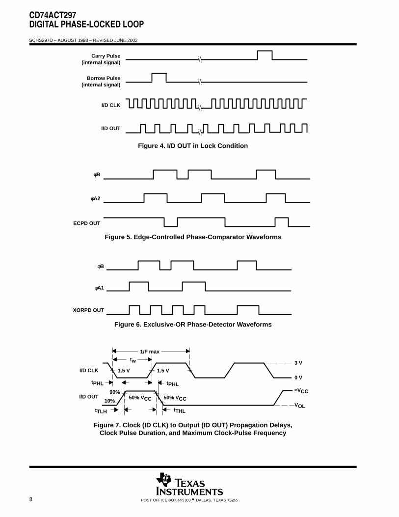
Carry Pulse(internal signal)
Borrow Pulse(internal signal)
I/D CLK
I/D OUT
Figure 4. I/D OUT in Lock Condition
φB
φA2
ECPD OUT
Figure 5. Edge-Controlled Phase-Comparator Waveforms
φB
φA1
XORPD OUT
Figure 6. Exclusive-OR Phase-Detector Waveforms
tTHL
tPHL
1/F max
I/D CLK
tPHL
I/D OUT
tTLH
50% VCC
tw
1.5 V 1.5 V
50% VCC10%
90%
3 V
0 V
VOL
≈VCC
Figure 7. Clock (ID CLK) to Output (ID OUT) Propagation Delays,Clock Pulse Duration, and Maximum Clock-Pulse Frequency
CD74ACT297DIGITAL PHASE-LOCKED LOOP
SCHS297D – AUGUST 1998 – REVISED JUNE 2002
9POST OFFICE BOX 655303 • DALLAS, TEXAS 75265
tPLH
tPHLtPLH
tPHL
φB
φA1
XORPD OUT
50% VCC
1.5 V
50% VCC 50% VCC 50% VCC
1.5 V
1.5 V 1.5 V3 V
0 V
3 V
0 V
VOL
≈VCC
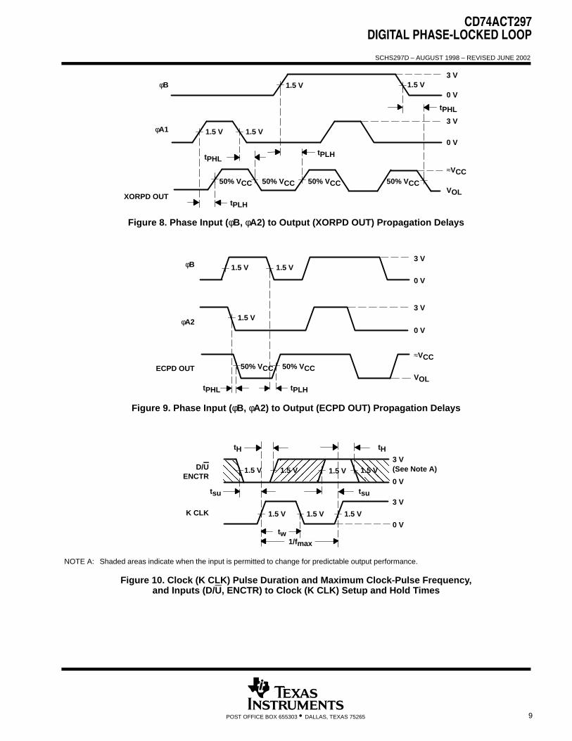
Figure 8. Phase Input (φB, φA2) to Output (XORPD OUT) Propagation Delays
φB
φA2
ECPD OUT
tPHL tPLH
3 V
0 V
VOL
≈VCC50% VCC
1.5 V
50% VCC
1.5 V
1.5 V
3 V
0 V
Figure 9. Phase Input (φB, φA2) to Output (ECPD OUT) Propagation Delays
ÏÏÏÏÏÏÏÏ
ÏÏÏÏ
ÎÎÎÎÎÎÎÎÎÎÎÎÎÎÎ
D/UENCTR
K CLK
1/fmax
tsu
tw
tsu
tHtH
NOTE A: Shaded areas indicate when the input is permitted to change for predictable output performance.
3 V
0 V
1.5 V 1.5 V 1.5 V 1.5 V
1.5 V 1.5 V 1.5 V
3 V
0 V
(See Note A)
Figure 10. Clock (K CLK) Pulse Duration and Maximum Clock-Pulse Frequency,and Inputs (D/U, ENCTR) to Clock (K CLK) Setup and Hold Times
CD74ACT297DIGITAL PHASE-LOCKED LOOP
SCHS297D – AUGUST 1998 – REVISED JUNE 2002
10 POST OFFICE BOX 655303 • DALLAS, TEXAS 75265
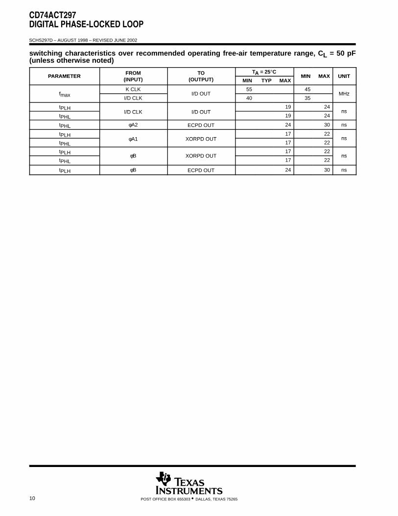
switching characteristics over recommended operating free-air temperature range, CL = 50 pF(unless otherwise noted)
PARAMETERFROM TO TA = 25°C
MIN MAX UNITPARAMETER(INPUT) (OUTPUT) MIN TYP MAX
MIN MAX UNIT
fK CLK
I/D OUT55 45
MHzfmaxI/D CLK
I/D OUT40 35
MHz
tPLHI/D CLK I/D OUT
19 24ns
tPHLI/D CLK I/D OUT
19 24ns
tPHL φA2 ECPD OUT 24 30 ns
tPLHφA1 XORPD OUT
17 22ns
tPHLφA1 XORPD OUT
17 22ns
tPLH φB XORPD OUT17 22
nstPHL
φB XORPD OUT17 22
ns
tPLH φB ECPD OUT 24 30 ns
CD74ACT297DIGITAL PHASE-LOCKED LOOP
SCHS297D – AUGUST 1998 – REVISED JUNE 2002
11POST OFFICE BOX 655303 • DALLAS, TEXAS 75265
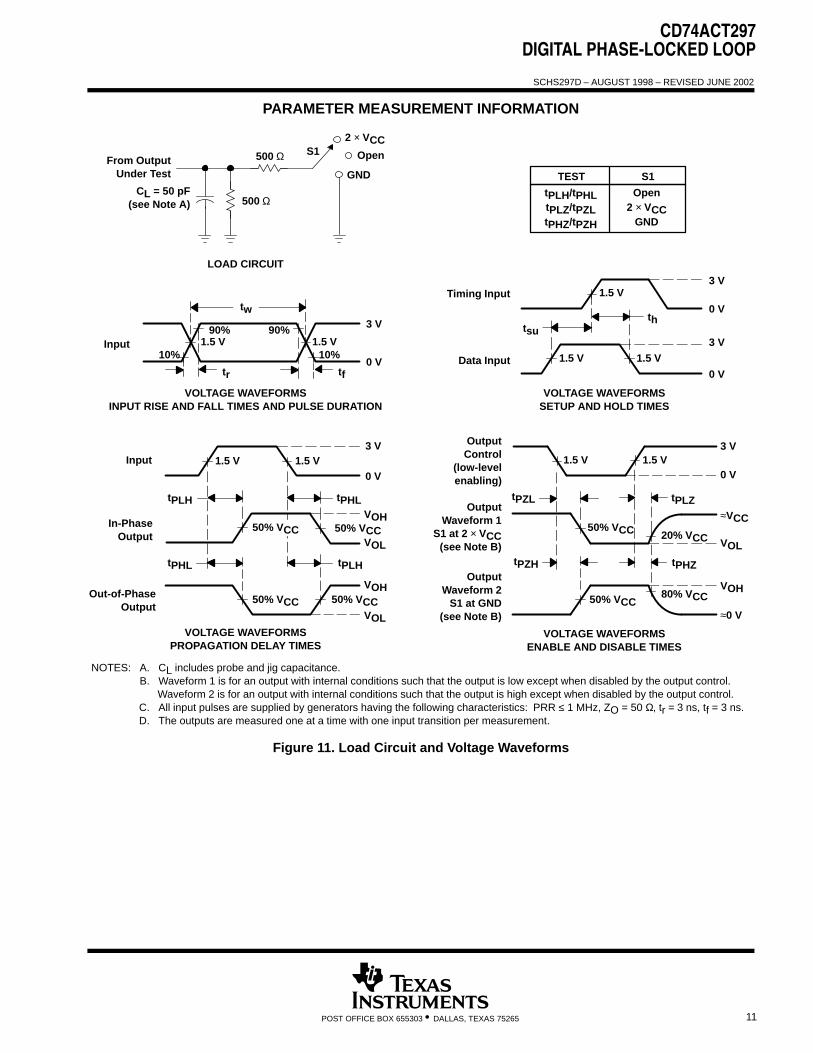
PARAMETER MEASUREMENT INFORMATION
50% VCC
3 V
3 V
0 V
0 V
thtsu
VOLTAGE WAVEFORMSSETUP AND HOLD TIMES
Data Input
tPLH
tPHL
tPHL
tPLH
VOH
VOH
VOL
VOL
3 V
0 V
50% VCC50% VCC
Input
Out-of-PhaseOutput
In-PhaseOutput
Timing Input
50% VCC
VOLTAGE WAVEFORMSPROPAGATION DELAY TIMES
From Output Under Test
CL = 50 pF(see Note A)
LOAD CIRCUIT
S12 × VCC
500 Ω
500 Ω
OutputControl
(low-levelenabling)
OutputWaveform 1
S1 at 2 × VCC(see Note B)
OutputWaveform 2
S1 at GND(see Note B)
VOL
VOH
tPZL
tPZH
tPLZ
tPHZ
≈VCC
0 V
50% VCC 20% VCC
50% VCC80% VCC
≈0 V
3 V
GND
Open
VOLTAGE WAVEFORMSENABLE AND DISABLE TIMES
tPLH/tPHLtPLZ/tPZLtPHZ/tPZH
Open2 × VCC
GND
TEST S1
3 V
0 V
tw
VOLTAGE WAVEFORMSINPUT RISE AND FALL TIMES AND PULSE DURATION
Input
NOTES: A. CL includes probe and jig capacitance.B. Waveform 1 is for an output with internal conditions such that the output is low except when disabled by the output control.
Waveform 2 is for an output with internal conditions such that the output is high except when disabled by the output control.C. All input pulses are supplied by generators having the following characteristics: PRR ≤ 1 MHz, ZO = 50 Ω, tr = 3 ns, tf = 3 ns.D. The outputs are measured one at a time with one input transition per measurement.
90% 90%
10%10%
tftr
1.5 V 1.5 V
1.5 V 1.5 V
1.5 V
1.5 V 1.5 V
1.5 V 1.5 V
Figure 11. Load Circuit and Voltage Waveforms

PACKAGE OPTION ADDENDUM
www.ti.com 10-Jun-2014
Addendum-Page 1
PACKAGING INFORMATION
Orderable Device Status(1)
Package Type PackageDrawing
Pins PackageQty
Eco Plan(2)
Lead/Ball Finish(6)
MSL Peak Temp(3)
Op Temp (°C) Device Marking(4/5)
Samples
CD74ACT297M ACTIVE SOIC D 16 40 Green (RoHS& no Sb/Br)
CU NIPDAU Level-1-260C-UNLIM -55 to 125 ACT297M
CD74ACT297M96 ACTIVE SOIC D 16 2500 Green (RoHS& no Sb/Br)
CU NIPDAU Level-1-260C-UNLIM -55 to 125 ACT297M
(1) The marketing status values are defined as follows:ACTIVE: Product device recommended for new designs.LIFEBUY: TI has announced that the device will be discontinued, and a lifetime-buy period is in effect.NRND: Not recommended for new designs. Device is in production to support existing customers, but TI does not recommend using this part in a new design.PREVIEW: Device has been announced but is not in production. Samples may or may not be available.OBSOLETE: TI has discontinued the production of the device.
(2) Eco Plan - The planned eco-friendly classification: Pb-Free (RoHS), Pb-Free (RoHS Exempt), or Green (RoHS & no Sb/Br) - please check http://www.ti.com/productcontent for the latest availabilityinformation and additional product content details.TBD: The Pb-Free/Green conversion plan has not been defined.Pb-Free (RoHS): TI's terms "Lead-Free" or "Pb-Free" mean semiconductor products that are compatible with the current RoHS requirements for all 6 substances, including the requirement thatlead not exceed 0.1% by weight in homogeneous materials. Where designed to be soldered at high temperatures, TI Pb-Free products are suitable for use in specified lead-free processes.Pb-Free (RoHS Exempt): This component has a RoHS exemption for either 1) lead-based flip-chip solder bumps used between the die and package, or 2) lead-based die adhesive used betweenthe die and leadframe. The component is otherwise considered Pb-Free (RoHS compatible) as defined above.Green (RoHS & no Sb/Br): TI defines "Green" to mean Pb-Free (RoHS compatible), and free of Bromine (Br) and Antimony (Sb) based flame retardants (Br or Sb do not exceed 0.1% by weightin homogeneous material)
(3) MSL, Peak Temp. - The Moisture Sensitivity Level rating according to the JEDEC industry standard classifications, and peak solder temperature.
(4) There may be additional marking, which relates to the logo, the lot trace code information, or the environmental category on the device.
(5) Multiple Device Markings will be inside parentheses. Only one Device Marking contained in parentheses and separated by a "~" will appear on a device. If a line is indented then it is a continuationof the previous line and the two combined represent the entire Device Marking for that device.
(6) Lead/Ball Finish - Orderable Devices may have multiple material finish options. Finish options are separated by a vertical ruled line. Lead/Ball Finish values may wrap to two lines if the finishvalue exceeds the maximum column width.
Important Information and Disclaimer:The information provided on this page represents TI's knowledge and belief as of the date that it is provided. TI bases its knowledge and belief on informationprovided by third parties, and makes no representation or warranty as to the accuracy of such information. Efforts are underway to better integrate information from third parties. TI has taken andcontinues to take reasonable steps to provide representative and accurate information but may not have conducted destructive testing or chemical analysis on incoming materials and chemicals.TI and TI suppliers consider certain information to be proprietary, and thus CAS numbers and other limited information may not be available for release.
PACKAGE OPTION ADDENDUM
www.ti.com 10-Jun-2014
Addendum-Page 2
In no event shall TI's liability arising out of such information exceed the total purchase price of the TI part(s) at issue in this document sold by TI to Customer on an annual basis.
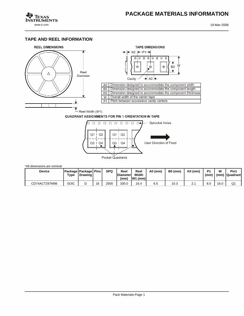
TAPE AND REEL INFORMATION
*All dimensions are nominal
Device PackageType
PackageDrawing
Pins SPQ ReelDiameter
(mm)
ReelWidth
W1 (mm)
A0 (mm) B0 (mm) K0 (mm) P1(mm)
W(mm)
Pin1Quadrant
CD74ACT297M96 SOIC D 16 2500 330.0 16.4 6.5 10.3 2.1 8.0 16.0 Q1
PACKAGE MATERIALS INFORMATION
www.ti.com 19-Mar-2008
Pack Materials-Page 1

*All dimensions are nominal
Device Package Type Package Drawing Pins SPQ Length (mm) Width (mm) Height (mm)
CD74ACT297M96 SOIC D 16 2500 333.2 345.9 28.6
PACKAGE MATERIALS INFORMATION
www.ti.com 19-Mar-2008
Pack Materials-Page 2
IMPORTANT NOTICETexas Instruments Incorporated and its subsidiaries (TI) reserve the right to make corrections, enhancements, improvements and otherchanges to its semiconductor products and services per JESD46, latest issue, and to discontinue any product or service per JESD48, latestissue. Buyers should obtain the latest relevant information before placing orders and should verify that such information is current andcomplete. All semiconductor products (also referred to herein as “components”) are sold subject to TI’s terms and conditions of salesupplied at the time of order acknowledgment.TI warrants performance of its components to the specifications applicable at the time of sale, in accordance with the warranty in TI’s termsand conditions of sale of semiconductor products. Testing and other quality control techniques are used to the extent TI deems necessaryto support this warranty. Except where mandated by applicable law, testing of all parameters of each component is not necessarilyperformed.TI assumes no liability for applications assistance or the design of Buyers’ products. Buyers are responsible for their products andapplications using TI components. To minimize the risks associated with Buyers’ products and applications, Buyers should provideadequate design and operating safeguards.TI does not warrant or represent that any license, either express or implied, is granted under any patent right, copyright, mask work right, orother intellectual property right relating to any combination, machine, or process in which TI components or services are used. Informationpublished by TI regarding third-party products or services does not constitute a license to use such products or services or a warranty orendorsement thereof. Use of such information may require a license from a third party under the patents or other intellectual property of thethird party, or a license from TI under the patents or other intellectual property of TI.Reproduction of significant portions of TI information in TI data books or data sheets is permissible only if reproduction is without alterationand is accompanied by all associated warranties, conditions, limitations, and notices. TI is not responsible or liable for such altereddocumentation. Information of third parties may be subject to additional restrictions.Resale of TI components or services with statements different from or beyond the parameters stated by TI for that component or servicevoids all express and any implied warranties for the associated TI component or service and is an unfair and deceptive business practice.TI is not responsible or liable for any such statements.Buyer acknowledges and agrees that it is solely responsible for compliance with all legal, regulatory and safety-related requirementsconcerning its products, and any use of TI components in its applications, notwithstanding any applications-related information or supportthat may be provided by TI. Buyer represents and agrees that it has all the necessary expertise to create and implement safeguards whichanticipate dangerous consequences of failures, monitor failures and their consequences, lessen the likelihood of failures that might causeharm and take appropriate remedial actions. Buyer will fully indemnify TI and its representatives against any damages arising out of the useof any TI components in safety-critical applications.In some cases, TI components may be promoted specifically to facilitate safety-related applications. With such components, TI’s goal is tohelp enable customers to design and create their own end-product solutions that meet applicable functional safety standards andrequirements. Nonetheless, such components are subject to these terms.No TI components are authorized for use in FDA Class III (or similar life-critical medical equipment) unless authorized officers of the partieshave executed a special agreement specifically governing such use.Only those TI components which TI has specifically designated as military grade or “enhanced plastic” are designed and intended for use inmilitary/aerospace applications or environments. Buyer acknowledges and agrees that any military or aerospace use of TI componentswhich have not been so designated is solely at the Buyer's risk, and that Buyer is solely responsible for compliance with all legal andregulatory requirements in connection with such use.TI has specifically designated certain components as meeting ISO/TS16949 requirements, mainly for automotive use. In any case of use ofnon-designated products, TI will not be responsible for any failure to meet ISO/TS16949.Products ApplicationsAudio www.ti.com/audio Automotive and Transportation www.ti.com/automotiveAmplifiers amplifier.ti.com Communications and Telecom www.ti.com/communicationsData Converters dataconverter.ti.com Computers and Peripherals www.ti.com/computersDLP® Products www.dlp.com Consumer Electronics www.ti.com/consumer-appsDSP dsp.ti.com Energy and Lighting www.ti.com/energyClocks and Timers www.ti.com/clocks Industrial www.ti.com/industrialInterface interface.ti.com Medical www.ti.com/medicalLogic logic.ti.com Security www.ti.com/securityPower Mgmt power.ti.com Space, Avionics and Defense www.ti.com/space-avionics-defenseMicrocontrollers microcontroller.ti.com Video and Imaging www.ti.com/videoRFID www.ti-rfid.comOMAP Applications Processors www.ti.com/omap TI E2E Community e2e.ti.comWireless Connectivity www.ti.com/wirelessconnectivity
Mailing Address: Texas Instruments, Post Office Box 655303, Dallas, Texas 75265Copyright © 2014, Texas Instruments Incorporated