
Digital Communication
51
Digital Communication Training Kit. 1 Mohammad Sharawi and Husam Abu-Ajwah Electronics Engineering Princess Sumaya University College for Technology (Royal Scientific Society) Amman–Jordan August 1999 1 c 2000 by Mohammad Sharawi and Husam Abu-Ajwah All rights Reserved. No part of this report is to be copied, reproduced, or distributed in anyway , without written consent of the Author. Contact: [email protected] or [email protected]
-
Upload
jivtesh-singh-kahlon -
Category
Documents
-
view
442 -
download
1
Transcript of Digital Communication

Digital Communication Training Kit.1
Mohammad Sharawi and Husam Abu-AjwahElectronics Engineering
Princess Sumaya UniversityCollege for Technology
(Royal Scientific Society)Amman–Jordan
August 1999
1 c©2000 by Mohammad Sharawi and Husam Abu-Ajwah All rights Reserved.No part of this report is to be copied, reproduced, or distributed in anyway, withoutwritten consent of the Author.Contact: [email protected] or [email protected]

1
To our Moms, and Dads.
AbstractThe aim of this project is to demonstrate three of the Digital
Modulation schemes used these days in Communications, which arethe FSK(Frequency Shift Keying), the PSK(Phase Shift Keying),and the QPSK(Quadrature Phase Shift Keying), and to design theelectronic circuits for these systems on a single PCB(Printed Cir-cuit Board). This board is to be used for educational purposes inthe Communications Lab at Princess Sumaya University College forTechnology.
This project includes:
1. Analysis and description for the main features of each of themodulation schemes.
2. Design and implementation of the electronic circuits for eachof the three systems.
3. Design and implementation of a variable repetitive 8-bit wordgenerator.
4. Design of the PCB Layout that would have the three systemsmounted on.
Contents
1 Introduction 5
2 Background 72.1 FSK Modulation . . . . . . . . . . . . . . . . . . . . . . . . . . 72.2 PSK Modulation . . . . . . . . . . . . . . . . . . . . . . . . . . . 112.3 QPSK Modulation . . . . . . . . . . . . . . . . . . . . . . . . . . 13
3 Circuit Design 183.1 Introduction . . . . . . . . . . . . . . . . . . . . . . . . . . . . . . 183.2 Universal Clock and Word Generator . . . . . . . . . . . . . . . . 18
3.2.1 The Universal Clock . . . . . . . . . . . . . . . . . . . . . 183.2.2 The Word Generator . . . . . . . . . . . . . . . . . . . . . 18
3.3 FSK System . . . . . . . . . . . . . . . . . . . . . . . . . . . . . 193.3.1 FSK Transmitter . . . . . . . . . . . . . . . . . . . . . . . 193.3.2 FSK Receiver . . . . . . . . . . . . . . . . . . . . . . . . 22
3.4 The PSK Systems . . . . . . . . . . . . . . . . . . . . . . . . . . 233.4.1 The PSK Transmitter . . . . . . . . . . . . . . . . . . . . 243.4.2 The PSK Receiver . . . . . . . . . . . . . . . . . . . . . . 253.4.3 Balanced Modulator (MC1496 IC) . . . . . . . . . . . . . 30
3.5 The QPSK System . . . . . . . . . . . . . . . . . . . . . . . . . 313.5.1 The Phase Shifter . . . . . . . . . . . . . . . . . . . . . . 343.5.2 The Demultiplexer and Multiplexer circuits . . . . . . . . 343.5.3 The QPSK Transmitter . . . . . . . . . . . . . . . . . . 373.5.4 The QPSK Receiver . . . . . . . . . . . . . . . . . . . . 383.5.5 PCB Design and Final Circuit Schematic . . . . . . . . . 40
4 Results 46
5 Conclusion and Further enhancements 475.1 Conclusion . . . . . . . . . . . . . . . . . . . . . . . . . . . . . . 475.2 Further Enhancements . . . . . . . . . . . . . . . . . . . . . . . 47
2

List of Figures
2.1 FSK signal Constellation. [Hay94] . . . . . . . . . . . . . . . . . 82.2 An FSK modulator block diagram. . . . . . . . . . . . . . . . . . 92.3 FSK demodulator block . . . . . . . . . . . . . . . . . . . . . . . 102.4 PLL block diagram. . . . . . . . . . . . . . . . . . . . . . . . . . 102.5 PSK signal Constellation. [Hay94] . . . . . . . . . . . . . . . . . 112.6 PSK Block diagram. . . . . . . . . . . . . . . . . . . . . . . . . . 122.7 PSK demodulator Block diagram. . . . . . . . . . . . . . . . . . . 132.8 The two possible QPSK signal Constellations. [Rap96] . . . . . . 142.9 QPSK signal constellation with its decision regions. [Hay94] . . . 142.10 QPSK Modulator Block diagram . . . . . . . . . . . . . . . . . . 152.11 QPSK Demodulator Block diagram . . . . . . . . . . . . . . . . . 162.12 Noise Performance in AWGN.[Hay94] . . . . . . . . . . . . . . . . 17
3.1 Universal Clock Circuit. . . . . . . . . . . . . . . . . . . . . . . . 193.2 Word Generator Circuit. . . . . . . . . . . . . . . . . . . . . . . . 203.3 Word Signal. . . . . . . . . . . . . . . . . . . . . . . . . . . . . . 203.4 Voltage Divider at VCO I/P. . . . . . . . . . . . . . . . . . . . . 213.5 DC Offset Circuit. . . . . . . . . . . . . . . . . . . . . . . . . . . 213.6 VCO Circuit. . . . . . . . . . . . . . . . . . . . . . . . . . . . . . 223.7 FSK Output Signal. . . . . . . . . . . . . . . . . . . . . . . . . . 233.8 PLL Circuit. . . . . . . . . . . . . . . . . . . . . . . . . . . . . . 243.9 FSK total Circuit. . . . . . . . . . . . . . . . . . . . . . . . . . . 253.10 PSK Transmitter Circuit. . . . . . . . . . . . . . . . . . . . . . . 263.11 PSK output signal. . . . . . . . . . . . . . . . . . . . . . . . . . . 263.12 PSK Receiver Circuit. . . . . . . . . . . . . . . . . . . . . . . . . 273.13 Sellen-Key Filter. . . . . . . . . . . . . . . . . . . . . . . . . . . . 283.14 In/Out signals of the PSK receiver. . . . . . . . . . . . . . . . . . 293.15 Leveling Circuit. . . . . . . . . . . . . . . . . . . . . . . . . . . . 293.16 Gilbert Cell . . . . . . . . . . . . . . . . . . . . . . . . . . . . . . 323.17 MC1496 IC schematic . . . . . . . . . . . . . . . . . . . . . . . . 333.18 Phase shift circuit . . . . . . . . . . . . . . . . . . . . . . . . . . 343.19 Simulated Demux Circuit . . . . . . . . . . . . . . . . . . . . . . 353.20 Implemented Demux circuit . . . . . . . . . . . . . . . . . . . . 353.21 The CLK,CLK, Word, Flipflop1(even) and flipflop2(odd) out-
puts for the simulated demultiplexer. . . . . . . . . . . . . . . . . 363.22 The Mux circuit . . . . . . . . . . . . . . . . . . . . . . . . . . . 363.23 Word in to demultiplexer, odd, even, word out from multiplexer
streams . . . . . . . . . . . . . . . . . . . . . . . . . . . . . . . . 363.24 The QPSK Transmitter Circuit . . . . . . . . . . . . . . . . . . . 373.25 The QPSK Transmitter Signal . . . . . . . . . . . . . . . . . . . 383.26 The QPSK receiver circuit . . . . . . . . . . . . . . . . . . . . . . 39
3

LIST OF FIGURES 4
3.27 QPSK receiver signals . . . . . . . . . . . . . . . . . . . . . . . . 393.28 The final output and the initial input . . . . . . . . . . . . . . . 403.29 The Circuit Schematic of the Module. . . . . . . . . . . . . . . . 423.30 The Circuit IC and Component Layout. . . . . . . . . . . . . . . 433.31 The PCB Layout, Layer (1). . . . . . . . . . . . . . . . . . . . . . 443.32 The PCB Layout, Layer (2). . . . . . . . . . . . . . . . . . . . . . 45
Chapter 1
Introduction
Through ages, man always tried to find a way for long distance commu-nication. Man used pigeons, and men riding horses to deliver mail. These twomethods were inefficient; the first was limited to certain directions that the pi-geons were trained to go to, and the latter took longer time for further distances.These methods were used till the 19th century, when Alexander Graham Bellsucceeded in performing the first wired telephone call (transmitting and electri-cal signal) in 1875. This invention revolutionized world communication.
Since the invention of the telephone, communications industry kepton growing and widening. Another important invention was accomplished byGuglielmo Marconi, who was the first to transmit electrical signals throughthe air, and then receive the transmitted signal using a receiver. The firsttransmission trough the Atlantic was in 1901 which opened the door for Radiobroadcasting.
In World War I&II, wireless radio was very important in commandand control of troops. Analog transmitting schemes were used. The aim was totransmit information signals (voice) via the air. This was accomplished usingAnalog Modulation, which can be defined as:
The process by which some characteristic of a carrier is varied inaccordance with a modulating wave (information signal) [Hay94]
The carrier frequency is usually a sinusoidal signal that has a frequency muchhigher than the highest frequency component of the information signal.
Right after World War II, the idea of having Global Wireless informa-tion transmission arose. The developed countries started their rally of launchingsatellites to ease global communications, by covering larger areas that receivesatellite transmission. Also the Digital Modulation technology started to de-velop.
Nowadays, modern mobile communication systems use digital modu-lation techniques. Advancements in VLSI (Very Large Scale Integration) andDSP (Digital Signal Processing) made digital modulation more coast efficientthan analog modulation. There are other advantages of digital modulationover analog modulation including greater noise immunity, robustness to chan-nel impairment, easier multiplexing, and greater security. Furthermore digital
5
CHAPTER 1. INTRODUCTION 6
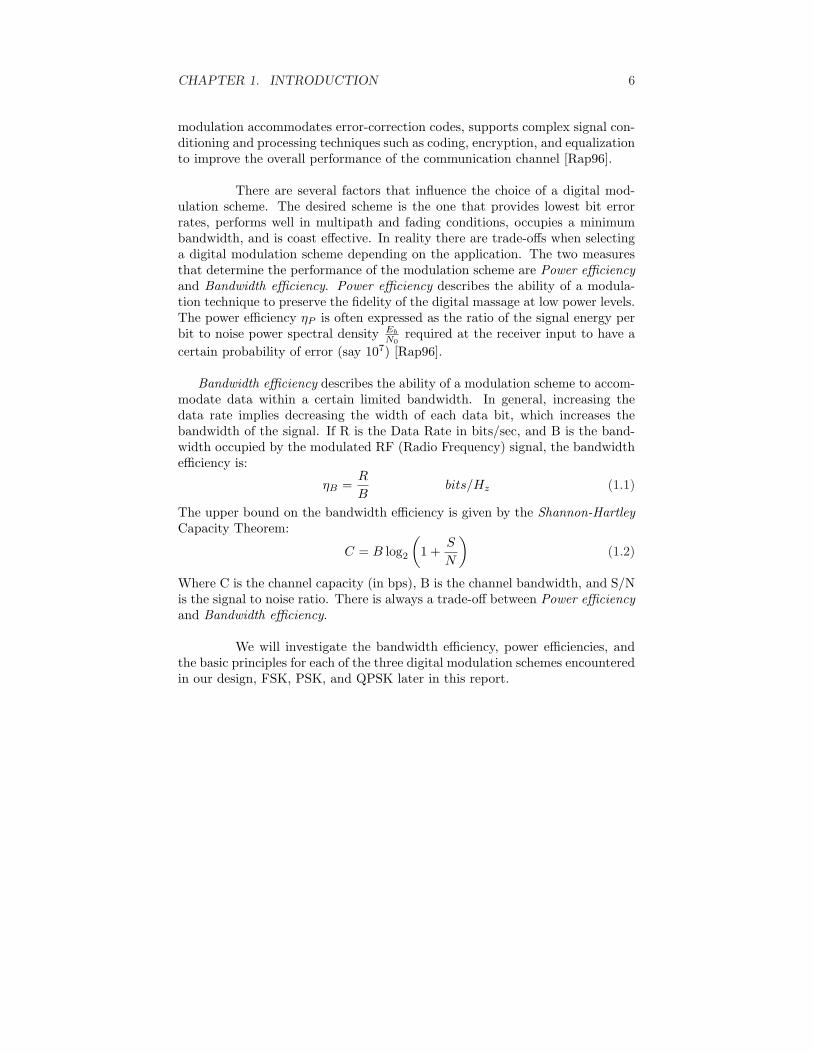
modulation accommodates error-correction codes, supports complex signal con-ditioning and processing techniques such as coding, encryption, and equalizationto improve the overall performance of the communication channel [Rap96].
There are several factors that influence the choice of a digital mod-ulation scheme. The desired scheme is the one that provides lowest bit errorrates, performs well in multipath and fading conditions, occupies a minimumbandwidth, and is coast effective. In reality there are trade-offs when selectinga digital modulation scheme depending on the application. The two measuresthat determine the performance of the modulation scheme are Power efficiencyand Bandwidth efficiency. Power efficiency describes the ability of a modula-tion technique to preserve the fidelity of the digital massage at low power levels.The power efficiency ηP is often expressed as the ratio of the signal energy perbit to noise power spectral density Eb
N0required at the receiver input to have a
certain probability of error (say 107) [Rap96].
Bandwidth efficiency describes the ability of a modulation scheme to accom-modate data within a certain limited bandwidth. In general, increasing thedata rate implies decreasing the width of each data bit, which increases thebandwidth of the signal. If R is the Data Rate in bits/sec, and B is the band-width occupied by the modulated RF (Radio Frequency) signal, the bandwidthefficiency is:
ηB =RB
bits/Hz (1.1)
The upper bound on the bandwidth efficiency is given by the Shannon-HartleyCapacity Theorem:
C = B log2
(
1 +SN
)
(1.2)
Where C is the channel capacity (in bps), B is the channel bandwidth, and S/Nis the signal to noise ratio. There is always a trade-off between Power efficiencyand Bandwidth efficiency.
We will investigate the bandwidth efficiency, power efficiencies, andthe basic principles for each of the three digital modulation schemes encounteredin our design, FSK, PSK, and QPSK later in this report.
Chapter 2
Background
This chapter will mainly describe the three Digital Modulation/Demodulationschemes used in our design, FSK, PSK, QPSK. It will specify the basic param-eters of each scheme, its equations, its block diagram, and its performance inAWGN(Additive White Gaussian Noise) channel.
2.1 FSK Modulation
The Frequency Shift Keying (FSK) scheme is used in new commercial datacommunication. Because of its close behavior to the FM modulation technique,FSK is replacing FM in the new digital based radio receivers because of thebenefits digital modulation has over analog ones, as we mentioned previously.As in FM, the amplitude of the FSK modulated signal is constant, but it’s thechanges in the frequency that carries the signal information. In general, an FSKsignal can be represented as:
si =
√
Eb
Tbcos(2πfit + θ)1 (0 ≤ t ≤ Tb), (i = 1, 2, 3, · · · ,M) (2.1)
where the frequency term fi will have M discrete values, and the term θ isan arbitrary constant, Tb is the bit time duration, and Eb is the energy perbit [Hay88]. In our design we are using Binary FSK, that uses two levels offrequencies, one is for transmitting a binary 1, the other is for transmittingbinary 0. The two signal equations in use are:
s0 =
√
Eb
Tbcos(2πf0t + θ) (2.2)
and,
s1 =
√
Eb
Tbcos(2πf1t + θ) (2.3)
where f0 is the frequency for transmitting a zero, and f1 is for transmitting aone. Such variations in the frequency due to the Digital input stream m(t) canbe obtained using a VCO.
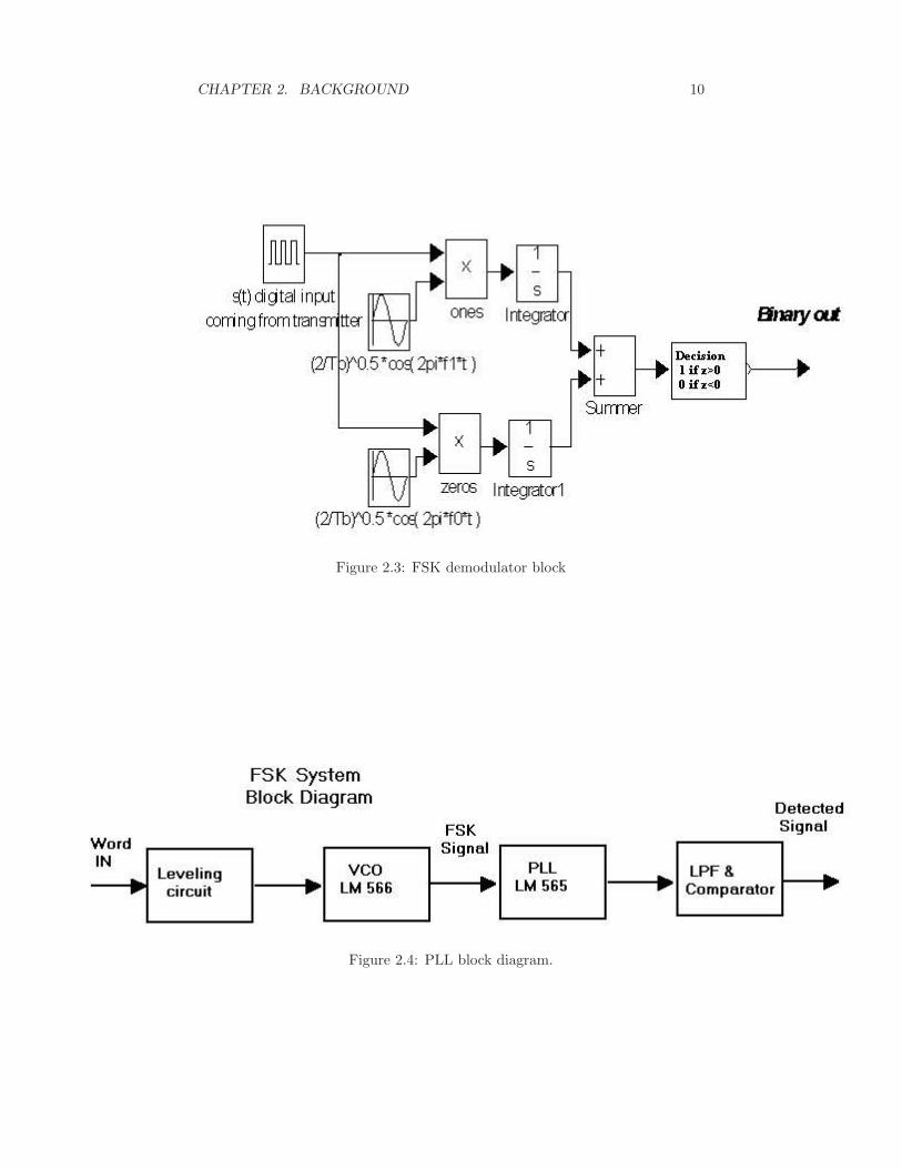
The Signal Constellation for the Binary FSK is shown in Fig.(2.1).Going to bandwidth issues, the transmission bandwidth of an FSK signal is
given by Carson’s rule:BT = 2∆f + 2B (2.4)
1Eb = 12A2
cTb , where Ac is the amplitude of the Carrier.
7

CHAPTER 2. BACKGROUND 8
Figure 2.1: FSK signal Constellation. [Hay94]
were B is the bandwidth of the digital baseband signal (information signal),and ∆f is the frequency deviation. Assuming the use of rectangular pulses, thismeans that B=R (R is the data rate), hence Eq.(2.5) becomes:
BT = 2(∆f + R) (2.5)
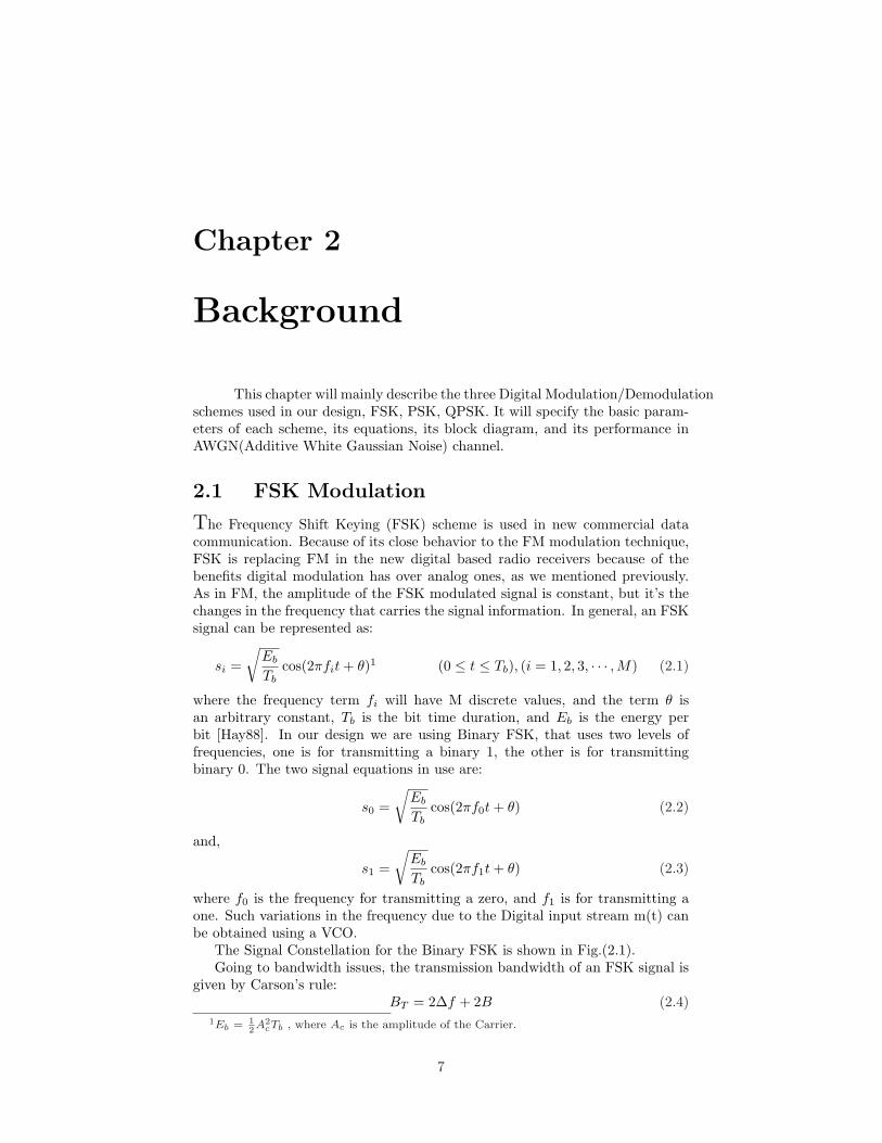
A block diagram for an FSK modulator is shown in Fig.(2.2).The average Probability of symbol error, or equivalently, the bit error rate
for coherent binary FSK is [Hay94]:
Pe =12
erfc
(√
Eb
2N0
)
2 (2.6)
were EbN0
is the signal energy per to noise power spectral density.An M-ary FSK signal consist of a set of Orthogonal3 set of M-frequency shiftedsignals. When these signals are detected coherently, the adjacent signals needto be separated by a frequency of 1
2T so as to maintain orthogonality. Hence wecan define the bandwidth of an M-FSK by:
B =M2T
(2.7)
For M-ary signals, the symbol duration is given by:
T = Tb log2 M (2.8)2Erfc is the complementary error function, were erfc(u) = 2√
π
∫∞u
e(−z)2 dz. Usually weuse tables to find its value. [Hay94]
3Two signals s1, s2 are orthogonal if:∫ T
0s1 ∗ s2 = 0. [Skl88]
CHAPTER 2. BACKGROUND 9
Figure 2.2: An FSK modulator block diagram.
where Tb is the bit duration. Now, substituting Eq.(2.8) in Eq.(2.7), we redefinethe channel bandwidth for and M-ary FSK signal as:
B =RbM
2 log2 M(2.9)
yielding a Bandwidth efficiency of:
ηB =2 log2 M
M(2.10)
Table 2.1 illustrates the bandwidth efficiency and the power efficiency of theM-levels for FSK Modulation: [Rap96]
M 2 4 8 16 32 64ηB bits/Hz 1 1 0.75 0.5 0.3125 0.1875
EbN0
for a BER of (10−6) 13.5 10.8 9.3 8.2 7.5 6.9
Table 2.1: The bandwidth efficiency and the power efficiency of the M-levelsFSK.
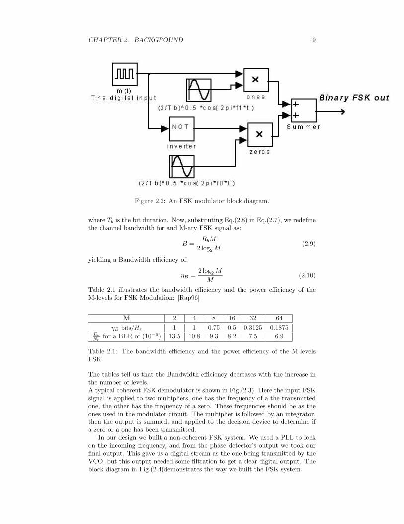
The tables tell us that the Bandwidth efficiency decreases with the increase inthe number of levels.A typical coherent FSK demodulator is shown in Fig.(2.3). Here the input FSKsignal is applied to two multipliers, one has the frequency of a the transmittedone, the other has the frequency of a zero. These frequencies should be as theones used in the modulator circuit. The multiplier is followed by an integrator,then the output is summed, and applied to the decision device to determine ifa zero or a one has been transmitted.
In our design we built a non-coherent FSK system. We used a PLL to lockon the incoming frequency, and from the phase detector’s output we took ourfinal output. This gave us a digital stream as the one being transmitted by theVCO, but this output needed some filtration to get a clear digital output. Theblock diagram in Fig.(2.4)demonstrates the way we built the FSK system.
CHAPTER 2. BACKGROUND 10
Figure 2.3: FSK demodulator block
Figure 2.4: PLL block diagram.
CHAPTER 2. BACKGROUND 11
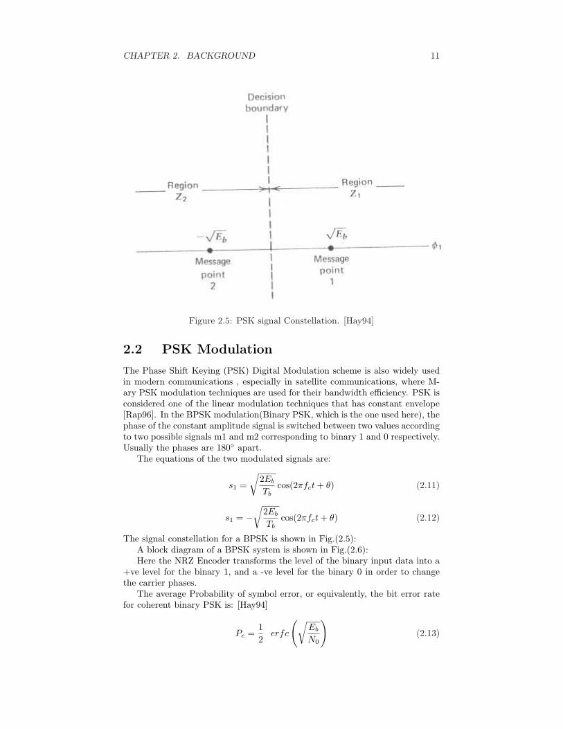
Figure 2.5: PSK signal Constellation. [Hay94]
2.2 PSK Modulation
The Phase Shift Keying (PSK) Digital Modulation scheme is also widely usedin modern communications , especially in satellite communications, where M-ary PSK modulation techniques are used for their bandwidth efficiency. PSK isconsidered one of the linear modulation techniques that has constant envelope[Rap96]. In the BPSK modulation(Binary PSK, which is the one used here), thephase of the constant amplitude signal is switched between two values accordingto two possible signals m1 and m2 corresponding to binary 1 and 0 respectively.Usually the phases are 180 apart.
The equations of the two modulated signals are:
s1 =
√
2Eb
Tbcos(2πfct + θ) (2.11)
s1 = −√
2Eb
Tbcos(2πfct + θ) (2.12)
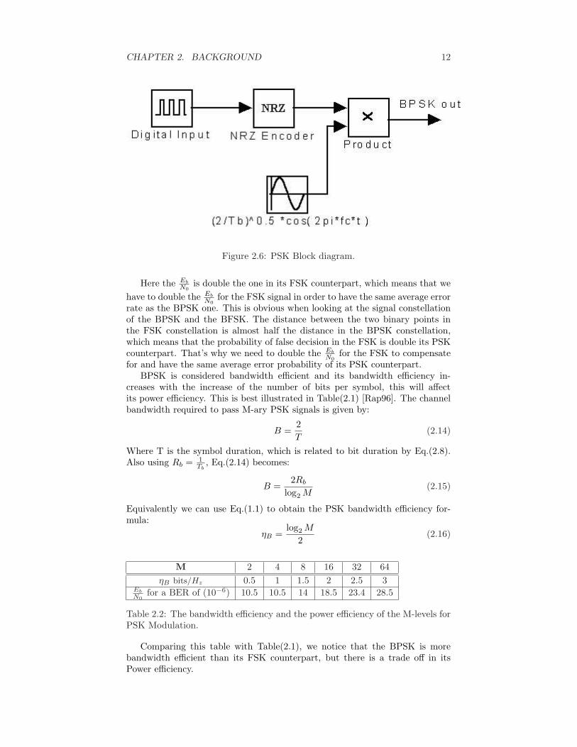
The signal constellation for a BPSK is shown in Fig.(2.5):A block diagram of a BPSK system is shown in Fig.(2.6):Here the NRZ Encoder transforms the level of the binary input data into a
+ve level for the binary 1, and a -ve level for the binary 0 in order to changethe carrier phases.
The average Probability of symbol error, or equivalently, the bit error ratefor coherent binary PSK is: [Hay94]
Pe =12
erfc
(√
Eb
N0
)
(2.13)
CHAPTER 2. BACKGROUND 12
Figure 2.6: PSK Block diagram.
Here the EbN0
is double the one in its FSK counterpart, which means that wehave to double the Eb
N0for the FSK signal in order to have the same average error
rate as the BPSK one. This is obvious when looking at the signal constellationof the BPSK and the BFSK. The distance between the two binary points inthe FSK constellation is almost half the distance in the BPSK constellation,which means that the probability of false decision in the FSK is double its PSKcounterpart. That’s why we need to double the Eb
N0for the FSK to compensate
for and have the same average error probability of its PSK counterpart.BPSK is considered bandwidth efficient and its bandwidth efficiency in-
creases with the increase of the number of bits per symbol, this will affectits power efficiency. This is best illustrated in Table(2.1) [Rap96]. The channelbandwidth required to pass M-ary PSK signals is given by:
B =2T
(2.14)
Where T is the symbol duration, which is related to bit duration by Eq.(2.8).Also using Rb = 1
Tb, Eq.(2.14) becomes:
B =2Rb
log2 M(2.15)
Equivalently we can use Eq.(1.1) to obtain the PSK bandwidth efficiency for-mula:
ηB =log2 M
2(2.16)
M 2 4 8 16 32 64ηB bits/Hz 0.5 1 1.5 2 2.5 3
EbN0
for a BER of (10−6) 10.5 10.5 14 18.5 23.4 28.5
Table 2.2: The bandwidth efficiency and the power efficiency of the M-levels forPSK Modulation.
Comparing this table with Table(2.1), we notice that the BPSK is morebandwidth efficient than its FSK counterpart, but there is a trade off in itsPower efficiency.

CHAPTER 2. BACKGROUND 13
Figure 2.7: PSK demodulator Block diagram.
As for the Demodulation process, For coherent detection, the basic demod-ulation scheme is shown in Fig.(2.7):
Here we have the incoming signal multiplied with a synchronized oscillatorthat has the same frequency of the modulation frequency. These two are multi-plied together, and the output is applied to a LPF (Low Pass Filter) to removenoise and to perform integration on the incoming signal. The decision devicefollows giving the Binary output.
In our design, we followed this basic modulator demodulator concept. Thecircuit design is shown in the coming chapter.
2.3 QPSK Modulation
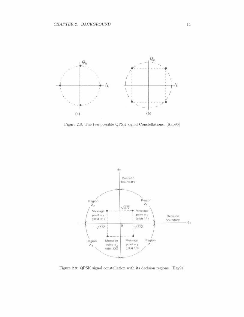
The Quadrature Phase Shift Keying (QPSK) is a 4-ary PSK signal. The QPSKis a modulation scheme widely used in Satellite Communications. As we men-tioned earlier, PSK signals are considered one of the linear modulation tech-niques, which are well known of their bandwidth efficiency.
The phase of the carrier in the QPSK takes 1 of 4 equally spaced shifts,such as 0, π
2 , π, 3π2 , where each value of phase corresponds to a unique pair of
message bits.The QPSK transmitted signal is defined by:
si =
√
Eb
Tbcos(2πfct + (i− 1)
π2
) (0 ≤ t ≤ Tb), (i = 1, 2, 3, 4) (2.17)
The signal Constellation of this equation is shown in fig (2.8a). Another wayof having a QPSK modulation is by using the phase shifts π
4 , 3π4 , 5π
4 , 7π4 . This
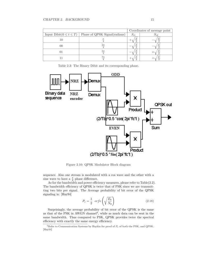
method yields the signal constellation as the shown in Fig.(2.8b). Also a tablethat shows the signal space characterization of the QPSK signaling is shown inTable (2.3).
As for the QPSK modulator (transmitter), the basic block diagram of sucha system is shown in Fig.(2.10):
In Fig.(2.10), the QPSK modulator consists of two streams of PSK mod-ulators, one is fed with the Odd data sequence, and the other with the even
CHAPTER 2. BACKGROUND 14
Figure 2.8: The two possible QPSK signal Constellations. [Rap96]
Figure 2.9: QPSK signal constellation with its decision regions. [Hay94]
CHAPTER 2. BACKGROUND 15
Coordinates of message pointInput Dibit(0 ≤ t ≤ T ) Phase of QPSK Signal(radians) Si1 Si2
10 π4 +
√
E2 −
√
E2
00 3π4 −
√
E2 −
√
E2
01 5π4 −
√
E2 +
√
E2
11 7π4 +
√
E2 +
√
E2
Table 2.3: The Binary Dibit and its corresponding phase.
Figure 2.10: QPSK Modulator Block diagram
sequence. Also one stream is modulated with a cos wave and the other with asine wave to have a π
2 phase difference.As for the bandwidth and power efficiency measures, please refer to Table(2.2).
The bandwidth efficiency of QPSK is twice that of PSK since we are transmit-ting two bits per signal. The Average probability of bit error of the QPSKsignaling is: [Hay94]
Pe =12
erfc
(√
Eb
N0
)
(2.18)
Surprisingly, the average probability of bit error of the QPSK is the sameas that of the PSK in AWGN channel4, while as much data can be sent in thesame bandwidth. Thus compared to PSK, QPSK provides twice the spectralefficiency with exactly the same energy efficiency.
4Refer to Communication Systems by Haykin for proof of Pe of both the PSK, and QPSK.[Hay94]
CHAPTER 2. BACKGROUND 16
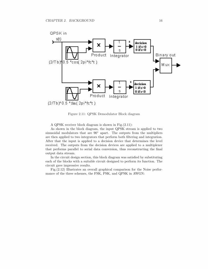
Figure 2.11: QPSK Demodulator Block diagram
A QPSK receiver block diagram is shown in Fig.(2.11):As shown in the block diagram, the input QPSK stream is applied to two
sinusoidal modulators that are 90 apart. The outputs from the multipliersare then applied to two integrators that perform both filtering and integration.After that the input is applied to a decision device that determines the levelreceived. The outputs from the decision devices are applied to a multiplexerthat performs parallel to serial data conversion, thus reconstructing the finaloutput data stream.
In the circuit design section, this block diagram was satisfied by substitutingeach of the blocks with a suitable circuit designed to perform its function. Thecircuit gave impressive results.
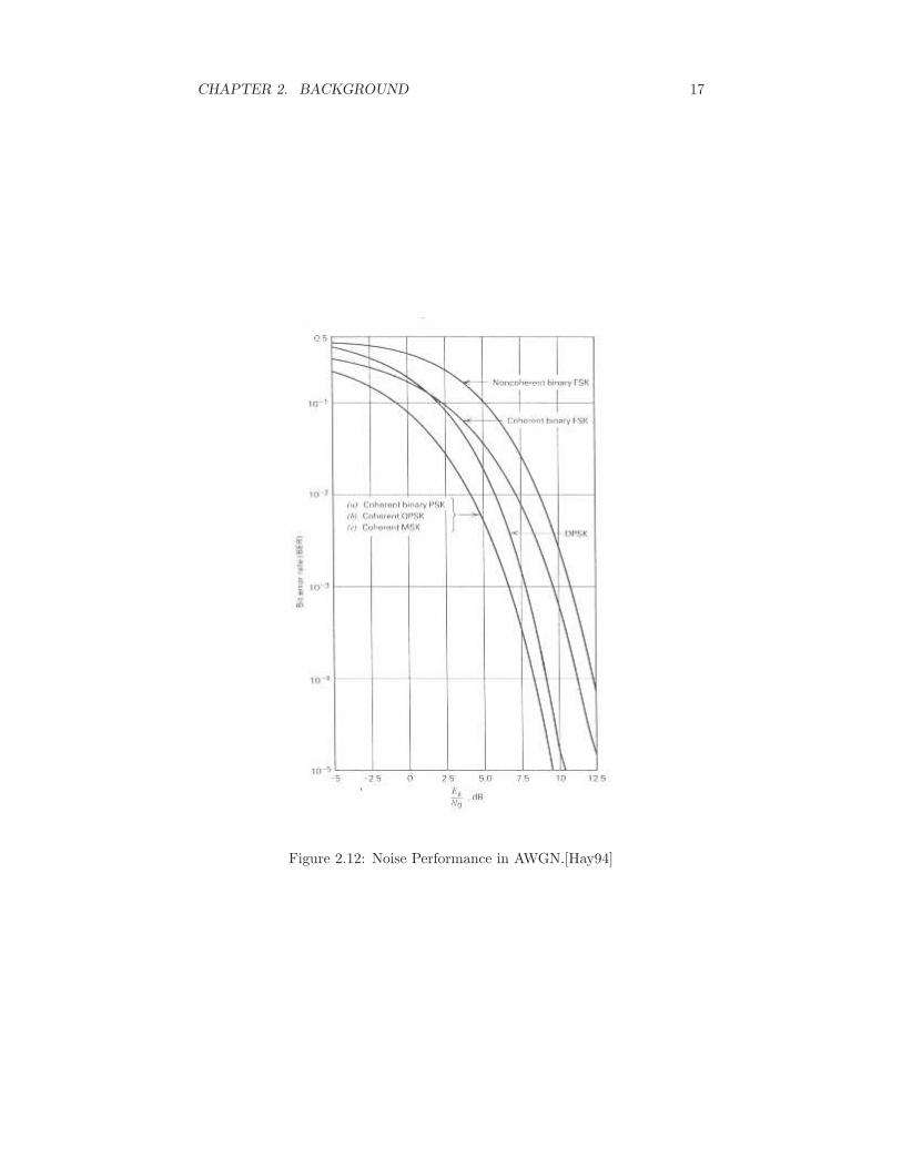
Fig.(2.12) Illustrates an overall graphical comparison for the Noise perfor-mance of the three schemes, the FSK, PSK, and QPSK in AWGN:
CHAPTER 2. BACKGROUND 17
Figure 2.12: Noise Performance in AWGN.[Hay94]
Chapter 3
Circuit Design
3.1 Introduction
Our project is composed of five major circuits which are : FSK ,PSK ,Q-PSKmodulators/demodulators, the Clock, and the Word generator. All mentionedcircuits were simulated by the Electronic Work Bench (EWB) simulation soft-ware. This chapter will illustrate each circuit with further information neededto show how these circuits were designed and why. Also we needed additionalcircuits such as, Attenuators, Filters, Comparators, Amplifiers, Phase shifter,Summer, Multiplexer and Demultiplexer were designed according to the appli-cation requirements.
The last part of this chapter shows the whole schematic of this project thathelps the student to find the places of the components for designed circuits in thischapter(every component is labeled so anyone can trace the circuit easily).Alsothe PCB design is shown in this part of the chapter. Limitations, requirementsand educational purposes of this design will be discussed to justify the reasonfor PCB board to appear the way it is.
3.2 Universal Clock and Word Generator
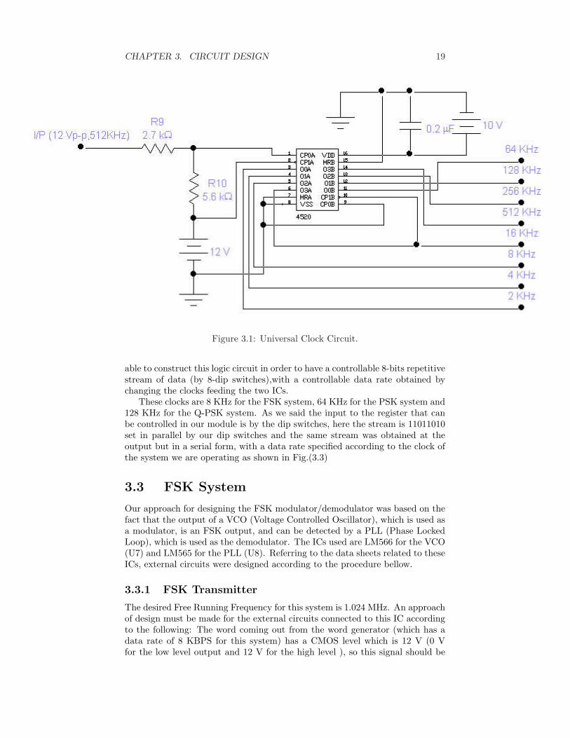
3.2.1 The Universal Clock
We will begin with the Universal clock circuit which consists of IC 4520 dualcounter as shown in Fig.(3.1):
A leveling circuit was built at the input, and by applying the super positionprinciple the output of the divider is 8V p− p (-4 V – 4 V), and the DC sourcecauses an offset of 4 V so the signal to the 4520 counter is from 0–8 V. This4520 counter will detect the 512 KHz input sine wave ,(gives logic high aboveits threshold which is 6 V and logic low bellow this level),and will give a CMOSsquare wave outputs with the frequencies of (2, 4, 8, 16, 64, 128, 256, 512 KHz)which are used in our system to control the data rate of the word coming outfrom the Word generator, and the clocks needed for the Multiplexer and theDemultiplexer circuits in the QPSK system.
3.2.2 The Word Generator
The word generator was implemented by using two ICs (4014 shift register,45164-bit counter), and by the referring to the data sheets for these two ICs, we were
18
CHAPTER 3. CIRCUIT DESIGN 19
Figure 3.1: Universal Clock Circuit.
able to construct this logic circuit in order to have a controllable 8-bits repetitivestream of data (by 8-dip switches),with a controllable data rate obtained bychanging the clocks feeding the two ICs.
These clocks are 8 KHz for the FSK system, 64 KHz for the PSK system and128 KHz for the Q-PSK system. As we said the input to the register that canbe controlled in our module is by the dip switches, here the stream is 11011010set in parallel by our dip switches and the same stream was obtained at theoutput but in a serial form, with a data rate specified according to the clock ofthe system we are operating as shown in Fig.(3.3)
3.3 FSK System
Our approach for designing the FSK modulator/demodulator was based on thefact that the output of a VCO (Voltage Controlled Oscillator), which is used asa modulator, is an FSK output, and can be detected by a PLL (Phase LockedLoop), which is used as the demodulator. The ICs used are LM566 for the VCO(U7) and LM565 for the PLL (U8). Referring to the data sheets related to theseICs, external circuits were designed according to the procedure bellow.
3.3.1 FSK Transmitter
The desired Free Running Frequency for this system is 1.024 MHz. An approachof design must be made for the external circuits connected to this IC accordingto the following: The word coming out from the word generator (which has adata rate of 8 KBPS for this system) has a CMOS level which is 12 V (0 Vfor the low level output and 12 V for the high level ), so this signal should be

CHAPTER 3. CIRCUIT DESIGN 20
Figure 3.2: Word Generator Circuit.
Figure 3.3: Word Signal.
CHAPTER 3. CIRCUIT DESIGN 21
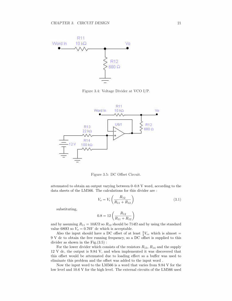
Figure 3.4: Voltage Divider at VCO I/P.
Figure 3.5: DC Offset Circuit.
attenuated to obtain an output varying between 0–0.8 V word, according to thedata sheets of the LM566. The calculations for this divider are :
Vo = Vi
(
R12
R11 + R12
)
(3.1)
substituting,
0.8 = 12(
R12
R11 + R12
)
and by assuming R11 = 10KΩ so R12 should be 714Ω and by using the standardvalue 680Ω so Vo = 0.76V dc which is acceptable.
Also the input should have a DC offset of at least 34Vcc which is almost =
9 V dc to obtain the free running frequency, so a DC offset is supplied to thisdivider as shown in the Fig.(3.5) :
For the lower divider which consists of the resistors R13, R14 and the supply12 V dc, the output is 9.84 V, and when implemented it was discovered thatthis offset would be attenuated due to loading effect so a buffer was used toeliminate this problem and the offset was added to the input word .
Now the input word to the LM566 is a word that varies from 9.84 V for thelow level and 10.6 V for the high level. The external circuits of the LM566 used
CHAPTER 3. CIRCUIT DESIGN 22
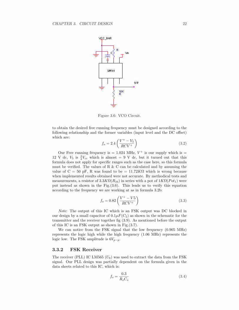
Figure 3.6: VCO Circuit.
to obtain the desired free running frequency must be designed according to thefollowing relationship and the former variables (input level and the DC offset)which are:
fo = 2.4(
V + − V5
RCV +
)
(3.2)
Our Free running frequency is = 1.024 MHz, V + is our supply which is =12 V dc, V5 is 3
4Vcc which is almost = 9 V dc, but it turned out that thisformula does not apply for specific ranges such as the case here, so this formulamust be verified. The values of R & C can be calculated and by assuming thevalue of C = 50 pF, R was found to be = 11.72KΩ which is wrong becausewhen implemented results obtained were not accurate. By methodical tests andmeasurements, a resistor of 3.3KΩ(R16) in series with a pot of 1KΩ(Pot1) wereput instead as shown in the Fig.(3.6). This leads us to verify this equationaccording to the frequency we are working at as in formula 3.2b:
fo = 0.82(
V + − V 5RCV +
)
(3.3)
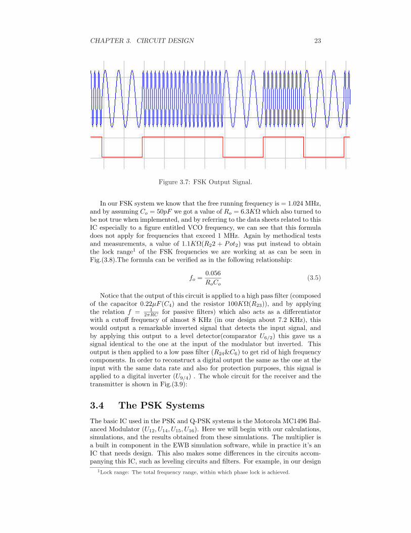
Note: The output of this IC which is an FSK output was DC blocked inour design by a small capacitor of 0.1µF (C2) as shown in the schematic for thetransmitter and the receiver together fig (3.9). As mentioned before the outputof this IC is an FSK output as shown in Fig.(3.7).
We can notice from the FSK signal that the low frequency (0.905 MHz)represents the logic high while the high frequency (1.06 MHz) represents thelogic low. The FSK amplitude is 6Vp−p.
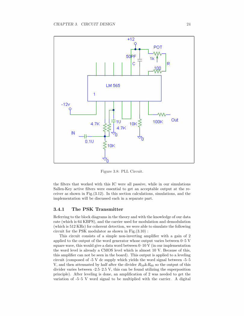
3.3.2 FSK Receiver
The receiver (PLL) IC LM565 (U8) was used to extract the data from the FSKsignal. Our PLL design was partially dependent on the formula given in thedata sheets related to this IC, which is:
fo =0.3
RoCo(3.4)
CHAPTER 3. CIRCUIT DESIGN 23
Figure 3.7: FSK Output Signal.
In our FSK system we know that the free running frequency is = 1.024 MHz,and by assuming Co = 50pF we got a value of Ro = 6.3KΩ which also turned tobe not true when implemented, and by referring to the data sheets related to thisIC especially to a figure entitled VCO frequency, we can see that this formuladoes not apply for frequencies that exceed 1 MHz. Again by methodical testsand measurements, a value of 1.1KΩ(R22 + Pot2) was put instead to obtainthe lock range1 of the FSK frequencies we are working at as can be seen inFig.(3.8).The formula can be verified as in the following relationship:
fo =0.056RoCo
(3.5)
Notice that the output of this circuit is applied to a high pass filter (composedof the capacitor 0.22µF (C4) and the resistor 100KΩ(R23)), and by applyingthe relation f = 1
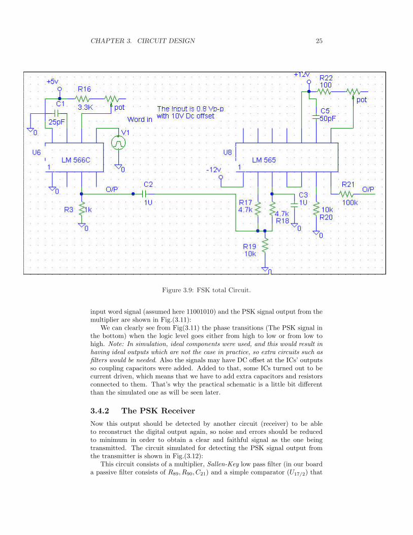
2πRC for passive filters) which also acts as a differentiatorwith a cutoff frequency of almost 8 KHz (in our design about 7.2 KHz), thiswould output a remarkable inverted signal that detects the input signal, andby applying this output to a level detector(comparator U6/2) this gave us asignal identical to the one at the input of the modulator but inverted. Thisoutput is then applied to a low pass filter (R24&C6) to get rid of high frequencycomponents. In order to reconstruct a digital output the same as the one at theinput with the same data rate and also for protection purposes, this signal isapplied to a digital inverter (U9/4) . The whole circuit for the receiver and thetransmitter is shown in Fig.(3.9):
3.4 The PSK Systems
The basic IC used in the PSK and Q-PSK systems is the Motorola MC1496 Bal-anced Modulator (U12, U14, U15, U16). Here we will begin with our calculations,simulations, and the results obtained from these simulations. The multiplier isa built in component in the EWB simulation software, while in practice it’s anIC that needs design. This also makes some differences in the circuits accom-panying this IC, such as leveling circuits and filters. For example, in our design
1Lock range: The total frequency range, within which phase lock is achieved.
CHAPTER 3. CIRCUIT DESIGN 24
Figure 3.8: PLL Circuit.
the filters that worked with this IC were all passive, while in our simulationsSallen-Key active filters were essential to get an acceptable output at the re-ceiver as shown in Fig.(3.12). In this section calculations, simulations, and theimplementation will be discussed each in a separate part.
3.4.1 The PSK Transmitter
Referring to the block diagrams in the theory and with the knowledge of our datarate (which is 64 KBPS), and the carrier used for modulation and demodulation(which is 512 KHz) for coherent detection, we were able to simulate the followingcircuit for the PSK modulator as shown in Fig.(3.10) :
This circuit consists of a simple non-inverting amplifier with a gain of 2applied to the output of the word generator whose output varies between 0–5 Vsquare wave, this would give a data word between 0–10 V (in our implementationthe word level is already a CMOS level which is almost 10 V. Because of this,this amplifier can not be seen in the board). This output is applied to a levelingcircuit (composed of -5 V dc supply which yields the word signal between -5–5V, and then attenuated by half after the divider R59&R60 so the output of thisdivider varies between -2.5–2.5 V, this can be found utilizing the superpositionprinciple). After leveling is done, an amplification of 2 was needed to get thevariation of -5–5 V word signal to be multiplied with the carrier. A digital
CHAPTER 3. CIRCUIT DESIGN 25
Figure 3.9: FSK total Circuit.
input word signal (assumed here 11001010) and the PSK signal output from themultiplier are shown in Fig.(3.11):
We can clearly see from Fig(3.11) the phase transitions (The PSK signal inthe bottom) when the logic level goes either from high to low or from low tohigh. Note: In simulation, ideal components were used, and this would result inhaving ideal outputs which are not the case in practice, so extra circuits such asfilters would be needed. Also the signals may have DC offset at the ICs’ outputsso coupling capacitors were added. Added to that, some ICs turned out to becurrent driven, which means that we have to add extra capacitors and resistorsconnected to them. That’s why the practical schematic is a little bit differentthan the simulated one as will be seen later.
3.4.2 The PSK Receiver
Now this output should be detected by another circuit (receiver) to be ableto reconstruct the digital output again, so noise and errors should be reducedto minimum in order to obtain a clear and faithful signal as the one beingtransmitted. The circuit simulated for detecting the PSK signal output fromthe transmitter is shown in Fig.(3.12):
This circuit consists of a multiplier, Sallen-Key low pass filter (in our boarda passive filter consists of R89, R90, C21) and a simple comparator (U17/2) that

CHAPTER 3. CIRCUIT DESIGN 26
Figure 3.10: PSK Transmitter Circuit.
Figure 3.11: PSK output signal.
CHAPTER 3. CIRCUIT DESIGN 27
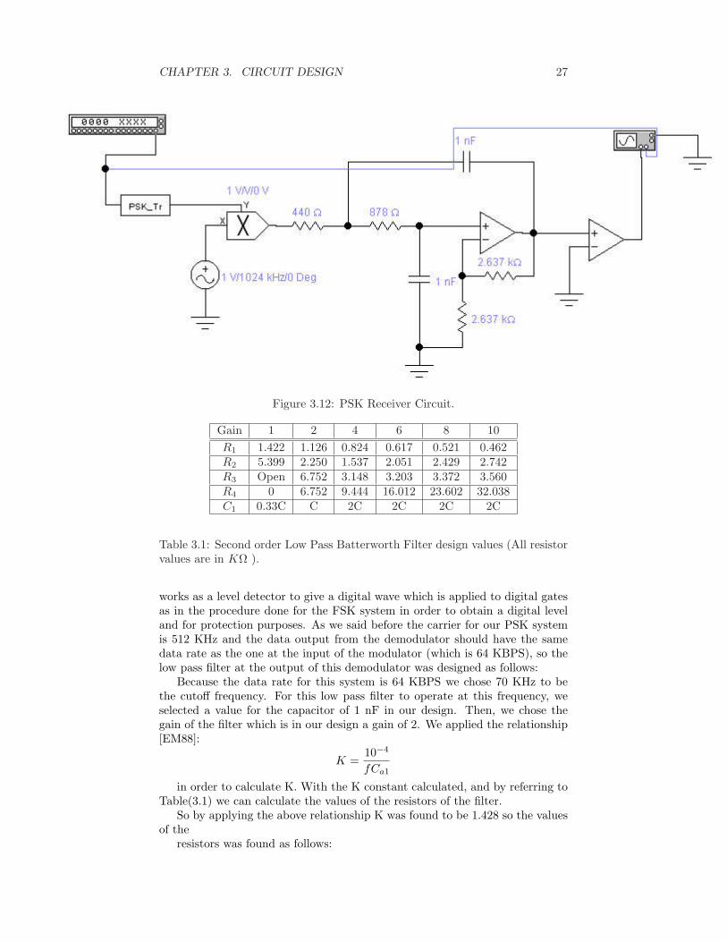
Figure 3.12: PSK Receiver Circuit.
Gain 1 2 4 6 8 10R1 1.422 1.126 0.824 0.617 0.521 0.462R2 5.399 2.250 1.537 2.051 2.429 2.742R3 Open 6.752 3.148 3.203 3.372 3.560R4 0 6.752 9.444 16.012 23.602 32.038C1 0.33C C 2C 2C 2C 2C
Table 3.1: Second order Low Pass Batterworth Filter design values (All resistorvalues are in KΩ ).
works as a level detector to give a digital wave which is applied to digital gatesas in the procedure done for the FSK system in order to obtain a digital leveland for protection purposes. As we said before the carrier for our PSK systemis 512 KHz and the data output from the demodulator should have the samedata rate as the one at the input of the modulator (which is 64 KBPS), so thelow pass filter at the output of this demodulator was designed as follows:
Because the data rate for this system is 64 KBPS we chose 70 KHz to bethe cutoff frequency. For this low pass filter to operate at this frequency, weselected a value for the capacitor of 1 nF in our design. Then, we chose thegain of the filter which is in our design a gain of 2. We applied the relationship[EM88]:
K =10−4
fCa1
in order to calculate K. With the K constant calculated, and by referring toTable(3.1) we can calculate the values of the resistors of the filter.
So by applying the above relationship K was found to be 1.428 so the valuesof the
resistors was found as follows:
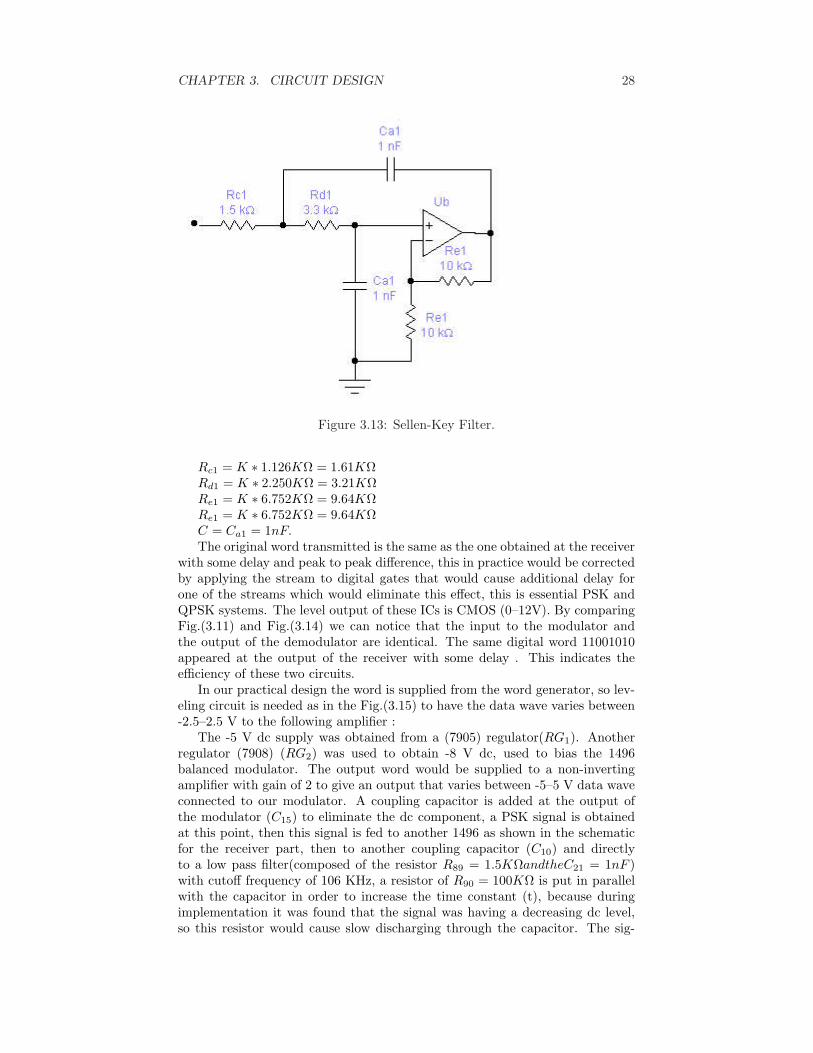
CHAPTER 3. CIRCUIT DESIGN 28
Figure 3.13: Sellen-Key Filter.
Rc1 = K ∗ 1.126KΩ = 1.61KΩRd1 = K ∗ 2.250KΩ = 3.21KΩRe1 = K ∗ 6.752KΩ = 9.64KΩRe1 = K ∗ 6.752KΩ = 9.64KΩC = Ca1 = 1nF.The original word transmitted is the same as the one obtained at the receiver
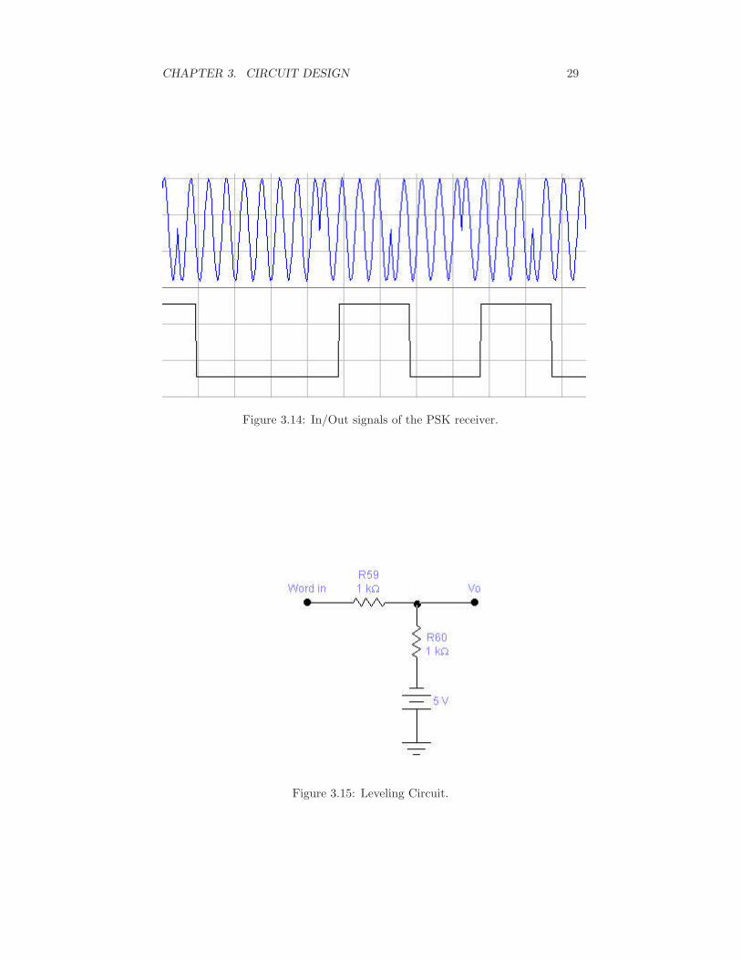
with some delay and peak to peak difference, this in practice would be correctedby applying the stream to digital gates that would cause additional delay forone of the streams which would eliminate this effect, this is essential PSK andQPSK systems. The level output of these ICs is CMOS (0–12V). By comparingFig.(3.11) and Fig.(3.14) we can notice that the input to the modulator andthe output of the demodulator are identical. The same digital word 11001010appeared at the output of the receiver with some delay . This indicates theefficiency of these two circuits.
In our practical design the word is supplied from the word generator, so lev-eling circuit is needed as in the Fig.(3.15) to have the data wave varies between-2.5–2.5 V to the following amplifier :
The -5 V dc supply was obtained from a (7905) regulator(RG1). Anotherregulator (7908) (RG2) was used to obtain -8 V dc, used to bias the 1496balanced modulator. The output word would be supplied to a non-invertingamplifier with gain of 2 to give an output that varies between -5–5 V data waveconnected to our modulator. A coupling capacitor is added at the output ofthe modulator (C15) to eliminate the dc component, a PSK signal is obtainedat this point, then this signal is fed to another 1496 as shown in the schematicfor the receiver part, then to another coupling capacitor (C10) and directlyto a low pass filter(composed of the resistor R89 = 1.5KΩandtheC21 = 1nF )with cutoff frequency of 106 KHz, a resistor of R90 = 100KΩ is put in parallelwith the capacitor in order to increase the time constant (t), because duringimplementation it was found that the signal was having a decreasing dc level,so this resistor would cause slow discharging through the capacitor. The sig-
CHAPTER 3. CIRCUIT DESIGN 29
Figure 3.14: In/Out signals of the PSK receiver.
Figure 3.15: Leveling Circuit.
CHAPTER 3. CIRCUIT DESIGN 30
nal is then applied to a non-inverting amplifier (U17/1) with gain of 11, to acomparator(U17/2) which would detect the signal to give an output identical tothe one at the input of the transmitter. The signal is then fed to a digital gatesuch as a D-flip flop(U19/1) to give a digital signal having the same bit durationas the one being transmitted. Another thing to mention here is that the carrieris taken directly from the function generator and should be attenuated to anappropriate level so that the balanced modulator would work properly, the levelof sine wave carrier coming from the function generator is 12Vp−p, this is thelevel the function generator was set to from the beginning and can be noticedin figure (3.1).
3.4.3 Balanced Modulator (MC1496 IC)
This IC is used as the multiplier block of the PSK, and the QPSK systems.This IC performs modulation using the two inputs to it. One of them is thecarrier signal, the other one is the information signal. The internal structure ofthis modulator is based on the Gilbert Cell multiplier circuit.
The values of the external components connected to this IC are obtainedusing the equations specified in the data sheet of the MC1496. As for the signalgain for low frequencies of operation, the following equation describes the gainbehavior(refer to the data sheet):
As =Vo
Vs=
RL
Re + 2re(3.6)
a gain of 1 is needed, ⇒ 1 = RLRe+2re
, and re = VTIE
= 25m
I5. For linear operation:
Vs ≤ I5Re (3.7)
referring to Fig.(3.16), and assuming that I5 = I6 = I92. and IB IC , then
R5 =V − − φ
I5− 500 , where φ = 0.75V at 25C (3.8)
We will use V − as -8.2V, which is taken from the 7908 Regulator output.The input current is assumed to be 1.22 mA(since at least 1 mA should flow inthe divider). Plugging these values in Eq.(3.8) yields:
R5 =8.2− 0.75
1.22m − 500 = 5.6KΩ
⇒ V5 = −6.8V = VBQ7 = VBQ8
⇒ IQ7 = IQ8 = IQ9
For Biasing, the following equations must be satisfied:
30V ≥ [(V6, V12)− (V7, V8)] ≥ 2V30V ≥ [(V7, V8)− (V1, V4)] ≥ 2.7V
30V ≥ [(V1, V4)− (V5)] ≥ 2.7V(3.9)
here V6 ≈ V12, V7 ≈ V8, V1 ≈ V4.If we use 2.7kΩ Load resistors at pins 6 and 12, then
VCQ6 = VCQ12 = 12V − (2.7k × 1.22m) = 8.706V2For a better circuit diagram, refer to the accompanied data sheet for the MC1496 IC
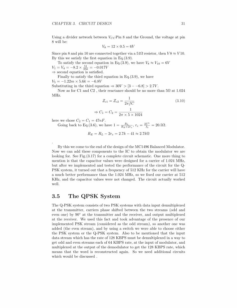
CHAPTER 3. CIRCUIT DESIGN 31
Using a divider network between VCCPin 8 and the Ground, the voltage at pin8 will be:
V8 = 12× 0.5 = 6V
Since pin 8 and pin 10 are connected together via a 51Ω resistor, then V 8 ≈ V 10.By this we satisfy the first equation in Eq.(3.9).
To satisfy the second equation in Eq.(3.9), we have V8 ≈ V10 = 6VV1 = V4 = −8.2× 51
25k = −0.017V⇒ second equation is satisfied.
Finally to satisfy the third equation in Eq.(3.9), we haveV5 = −1.22m× 5.6k = −6.8VSubstituting in the third equation ⇒ 30V > [3−−6.8] > 2.7V .
Now as for C1 and C2 , their reactance should be no more than 5Ω at 1.024MHz.
Zc1 = Zc2 =1
2πfC(3.10)
⇒ C1 = C2 =1
2π × 5× 1024here we chose C2 = C1 = 47nF .
Going back to Eq.(3.6), we have 1 = RLRE+2re
, re = 25m
I5= 20.5Ω.
RE = RL − 2re = 2.7k − 41 ≈ 2.7kΩ
.By this we come to the end of the design of the MC1496 Balanced Modulator.
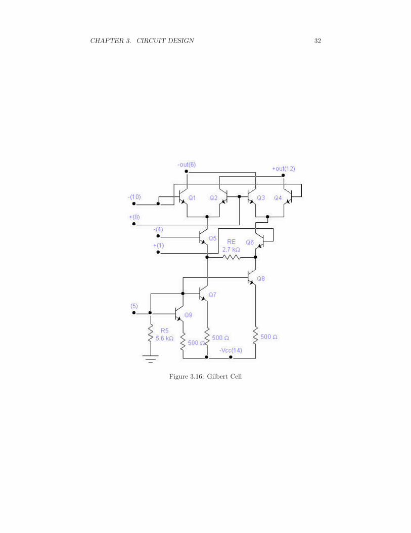
Now we can add these components to the IC to obtain the modulator we arelooking for. See Fig.(3.17) for a complete circuit schematic. One more thing tomention is that the capacitor values were designed for a carrier of 1.024 MHz,but after we implemented and tested the performance of the circuit for the Q-PSK system, it turned out that a frequency of 512 KHz for the carrier will havea much better performance than the 1.024 MHz, so we fixed our carrier at 512KHz, and the capacitor values were not changed. The circuit actually workedwell.
3.5 The QPSK System
The Q-PSK system consists of two PSK systems with data input demultiplexedat the transmitter, carriers phase shifted between the two streams (odd andeven one) by 90 at the transmitter and the receiver, and output multiplexedat the receiver. We used this fact and took advantage of the presence of ourimplemented PSK stream (considered as the odd stream), so another one wasadded (the even stream), and by using a switch we were able to choose eitherthe PSK system or the Q-PSK system. Also to be mentioned that the inputdata stream which has the rate of 128 KBPS must be demultiplexed in a way toget odd and even streams each of 64 KBPS rate, at the input of modulator, andmultiplexed at the output of the demodulator to get the 128 KBPS rate, whichmeans that the word is reconstructed again. So we need additional circuitswhich would be discussed .
CHAPTER 3. CIRCUIT DESIGN 32
Figure 3.16: Gilbert Cell
CHAPTER 3. CIRCUIT DESIGN 33
Figure 3.17: MC1496 IC schematic

CHAPTER 3. CIRCUIT DESIGN 34
Figure 3.18: Phase shift circuit
3.5.1 The Phase Shifter
We will begin with the phase shifter, which consists of two consecutive low passfilters. The transfer function of the two consecutive low pass filters is given by:
H(s) =1
(1 + SR55C12)(1 + SR56C13)(3.11)
This transfer function has two poles, the first one occurs at 1R55C12
and the otherat 1
R56C13. A Bode Plot of a low pass filter illustrates a 45 phase shift between
the input and the output at the pole. Since we have two consecutive low passfilters, this means that the output signal of such a combination will be 90
phase shifted from the input signal. We chose R55 = R56 = 680Ω, and C12 =C13 = 1nF , this gave us a double pole at 1.4 MHz. A remarkably attenuatedsine wave of 2.1Vp−p with almost 90 phase shift was obtained. The output ofthis phase shifter was connected to one stream as is (the even stream), whilethe other carrier input was attenuated to a level (by the divider R57 = 1.5kΩand R58 = 330Ω as shown on the schematic) almost 1
5 of the one from thefunction generator to get a carrier equal to the one at the output of this phaseshifter, which would be then applied to the other stream (the odd stream). Thecarrier applied from the function generator was 12Vp − p, and the output was2.1Vp−p after the phase shifter (when measured it was found 1.2V dc because ofloading effect when connected to the multiplier). This was proved by the formersimulation for the phase shifter, at 512 KHz the attenuation was almost 15 dBon the bode plotter while in calculations was as follows:
dB = 20Log(Vi
Vo) = 20Log(
122.1
) = 15.1dB
so the voltage divider must output a signal almost identical to the one at theoutput of this phase shifter. In the Q-PSK simulation, there was no need tosimulate phase shifting because we were able to apply two cosine waves withphase shift of 90 at the multiplier as can be shown in Figures (3.24) and (3.26).
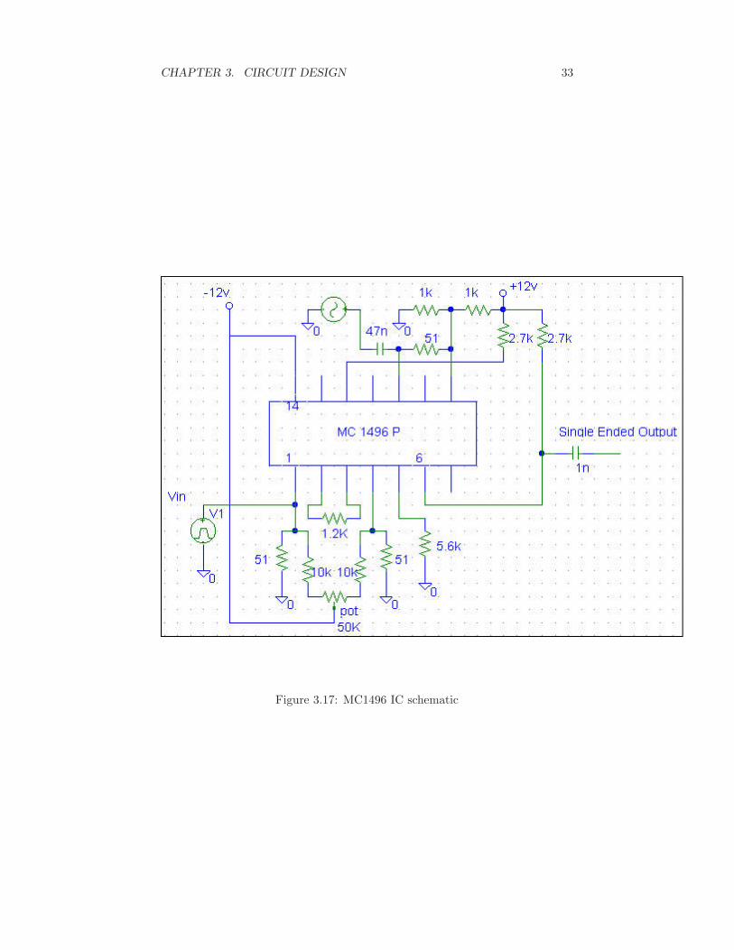
3.5.2 The Demultiplexer and Multiplexer circuits
Two additional circuits were added to this system, one was the demultiplexerand the other was the multiplexer circuit. These two circuits were used at thetransmitter and the receiver respectively. The main function of these circuits isfor serial to parallel conversion at the transmitter of the incoming data streamto be applied to the separate paths Q-PSK system, and the other serves as the
CHAPTER 3. CIRCUIT DESIGN 35
Figure 3.19: Simulated Demux Circuit
Figure 3.20: Implemented Demux circuit
parallel to serial conversion at the receiver .This can be illustrated from thedemultiplexer circuit in Fig.(3.19) and the multiplexer circuit in Fig.(3.22) Aswe said before data for the Q-PSK system needs to be demultiplexed at theinput of the transmitter. The input data rate is 128 KBPS for a word 01101000assumed for simulation. The thing needed here is to have two streams even andodd one each of 64 KBPS as follows :The even stream is 1000 and the odd one is 0110. We can notice that the clockfor the upper flip flop which is 64 KHz is the inverted clock of the lower one,this caused the input word to be separated into two different streams each of64 KBPS. Simulated output proved that the even stream lags the odd one witha bit duration of 7.8µs (half a bit), and to have the first bit of the even streamarrive to the upper multiplier at the same instant the first bit of the odd onedoes, an additional flip flop with a clock of 128 KHz was added to the lowerstream to correct this delay other wise incorrect results would be obtained atthe output of the Q-PSK transmitter as can be seen in Fig.(3.19). Anotherthing, in our board the last flip flop’s clock was of 64 KHz added to the upperstream not to the lower one, this is because in practice the delay was found tobe of bigger duration than simulation (delay of 1 bit) in the odd stream not inthe even one(so the even stream should be delayed) as can be seen in Fig.(3.20)which might be caused by the components in the circuit which would never workideally as in simulation.
Notice from Fig.(3.21):
1. The first two outputs which are the clocks, each of 64 KHz with inverted

CHAPTER 3. CIRCUIT DESIGN 36
Figure 3.21: The CLK,CLK, Word, Flipflop1(even) and flipflop2(odd) outputsfor the simulated demultiplexer.
Figure 3.22: The Mux circuit
wave forms.
2. The third output which is the input word 01101000 of 128 KHz.
3. Also we can notice from the last two outputs that they both begin atthe same instant of time (at the first positive edge of the inverted clock). Before the addition of the delay flip flop to the lower stream, theflipflop2’s output (the fifth wave form) appeared half a bit earlier, (at thefirst positive edge of the clock) this is why this flip flop of clock 128 KHzwas added to the lower one. The even stream output 1000 and the oddstream output 0110 each of 64 KBPS both begins now at the first positiveedge of the inverted clock as desired to be transmitted by the transmitter.
Now, these even and odd streams must be reconstructed again at the receiverafter the demodulators as can be seen later in the receiver part, but let’s assumefor the while that the same streams were obtained at these specific outputs(which are1000 for even and 0110 for odd) for illustration purposes, a circuitcalled multiplexer was used to mix these two streams into one (parallel to serialconversion) to obtain the original input serial word from the word generatorwhich is 01101000 as can be seen in Fig.(3.22). We can notice from Fig.(3.23)
Figure 3.23: Word in to demultiplexer, odd, even, word out from multiplexerstreams
CHAPTER 3. CIRCUIT DESIGN 37
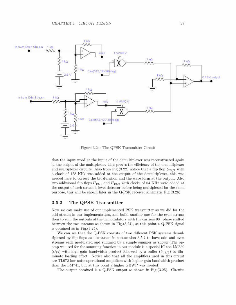
Figure 3.24: The QPSK Transmitter Circuit
that the input word at the input of the demultiplexer was reconstructed againat the output of the multiplexer. This proves the efficiency of the demultiplexerand multiplexer circuits. Also from Fig.(3.22) notice that a flip flop U22/1 witha clock of 128 KHz was added at the output of the demultiplexer, this wasneeded here to correct the bit duration and the wave form at the output. Alsotwo additional flip flops U19/1 and U19/2 with clocks of 64 KHz were added atthe output of each stream’s level detector before being multiplexed for the samepurpose, this will be shown later in the Q-PSK receiver schematic Fig.(3.26).
3.5.3 The QPSK Transmitter
Now we can make use of our implemented PSK transmitter as we did for theodd stream in our implementation, and build another one for the even streamthen to sum the outputs of the demodulators with the carriers 90 phase shiftedbetween the two streams as shown in Fig.(3.24), at this point a Q-PSK signalis obtained as in Fig.(3.25).
We can see that the Q-PSK consists of two different PSK systems demul-tiplexed by flip flops as illustrated in sub section 3.5.2 to have odd and evenstreams each modulated and summed by a simple summer as shown.(The op-amp we used for the summing function in our module is a special IC the LM359(U13) with high gain bandwidth product followed by a buffer (U11/2) to illu-minate loading effect. Notice also that all the amplifiers used in this circuitare TL072 low noise operational amplifiers with higher gain bandwidth productthan the LM741, but at this point a higher GBWP was needed).
The output obtained is a Q-PSK output as shown in Fig.(3.25). Circuits

CHAPTER 3. CIRCUIT DESIGN 38
Figure 3.25: The QPSK Transmitter Signal
used for the Q-PSK system after the demultiplexer are the same ones used forthe PSK system, so there is no need to discuss them again. To be mentionedhere is the difference in leveling circuits, in PSK simulations we amplified thesignal coming out from the word generator (TTL word) to get a level of 10 Vdata word because in implementation the word level is also of CMOS level, herein the Q-PSK system the flip flops used (in simulation) for the demultiplexer areTTL flip flops so the output level is a TTL level which is 5 V, leveling should bemade according to this output which is not the case in implementation wherethe output level of the flip flops used are of CMOS level . In other words inour implementation the DC level was -5 V dc needed after the CMOS flip flopswhich is the same in PSK circuits while in simulation for the Q-PSK system thelevel is -2.5 V dc needed after the TTL flip flops .
By referring to the data sheets of the IC LM359 ,it was found that capaci-tors of 1 nF each should be connected at the inputs of the summer (C16, C17),and during implementation a small capacitor of 100 pF (C18) was connectedto ground at the output in order to voltage drive this output (current drivenoutput) and not enough to drive the following buffer (U11/2).
3.5.4 The QPSK Receiver
The output of the summer was applied to two streams of PSK receivers whosecarriers are also shifted by 90, and then multiplexed at the output to be able toreconstruct the same digital word transmitted. The receiver circuit is illustratedin Fig.(3.26). Fig.(3.27) illustrates the Q-PSK signal at the input of receiverand the digital signal obtained at the output . Fig.(3.28) shows the input wordat the transmitter and the output word from the receiver which are identical,this proves the efficiency of these circuits. As we said before circuits here donot need illustration again because they were all discussed in the PSK receiverand the multiplexer subsections.
Two flip flops (U19/1 and U19/2) of 64 KHz were added at the output ofthe circuit shown in Fig.(3.26) before the multiplexer circuit to overcome bitduration and timing problems. An extra flip flop Uc of 64 KHz appears herein the schematic, this is because while simulation a delay of 1 bit to the evenstream was needed to enable the odd stream arrive to the multiplexer circuit 1bit earlier to mix together in a way that would reconstruct the input word againwith the rate of 128 KBPS, (this Uc was not used when implemented becausethe odd stream was already delayed by 1 bit which is needed and inverted so in

CHAPTER 3. CIRCUIT DESIGN 39
Figure 3.26: The QPSK receiver circuit
Figure 3.27: QPSK receiver signals
CHAPTER 3. CIRCUIT DESIGN 40
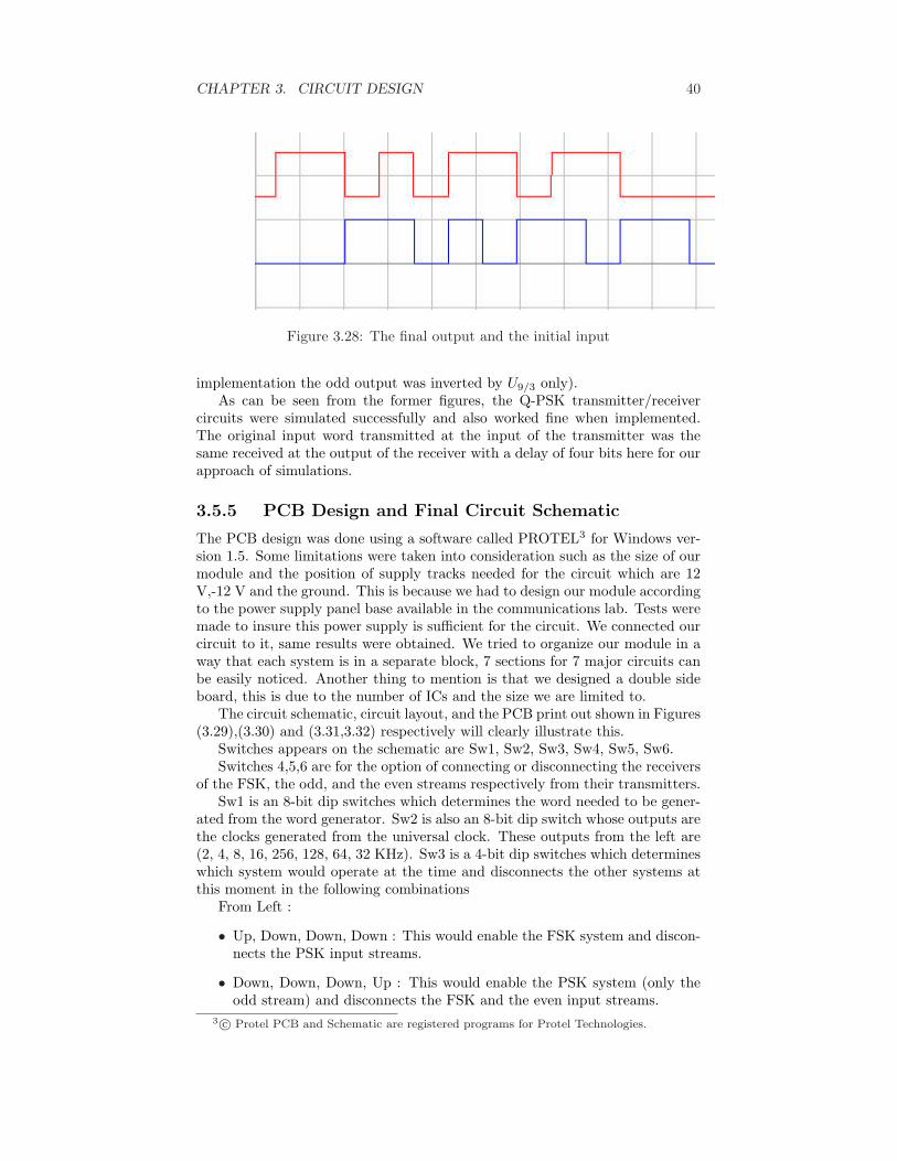
Figure 3.28: The final output and the initial input
implementation the odd output was inverted by U9/3 only).As can be seen from the former figures, the Q-PSK transmitter/receiver
circuits were simulated successfully and also worked fine when implemented.The original input word transmitted at the input of the transmitter was thesame received at the output of the receiver with a delay of four bits here for ourapproach of simulations.
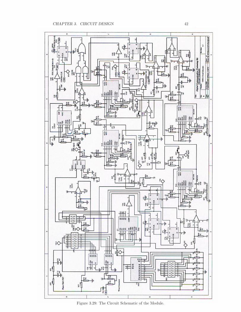
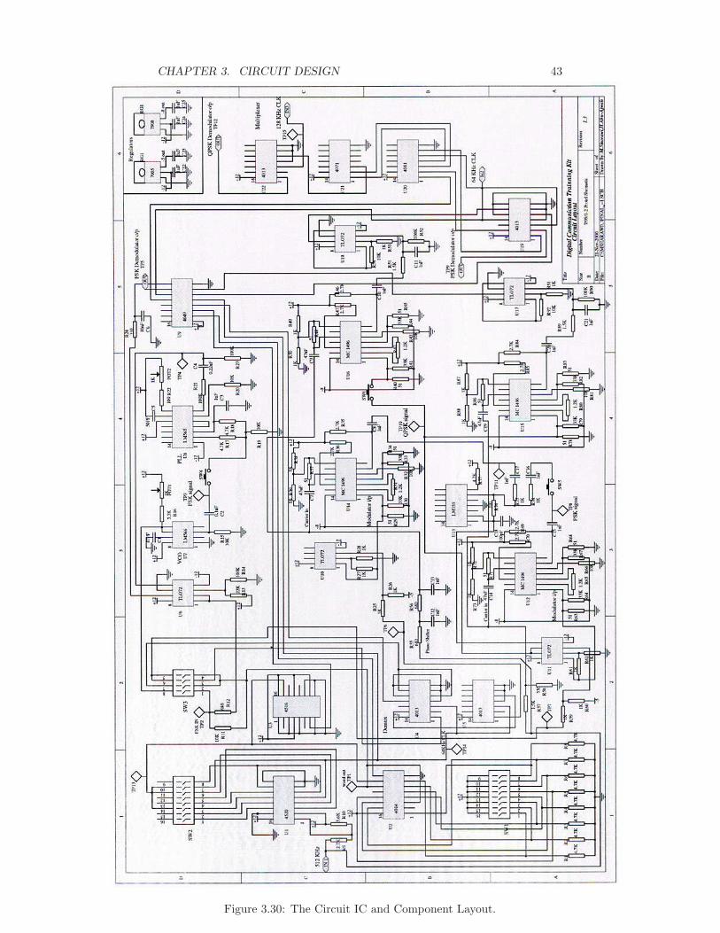
3.5.5 PCB Design and Final Circuit Schematic
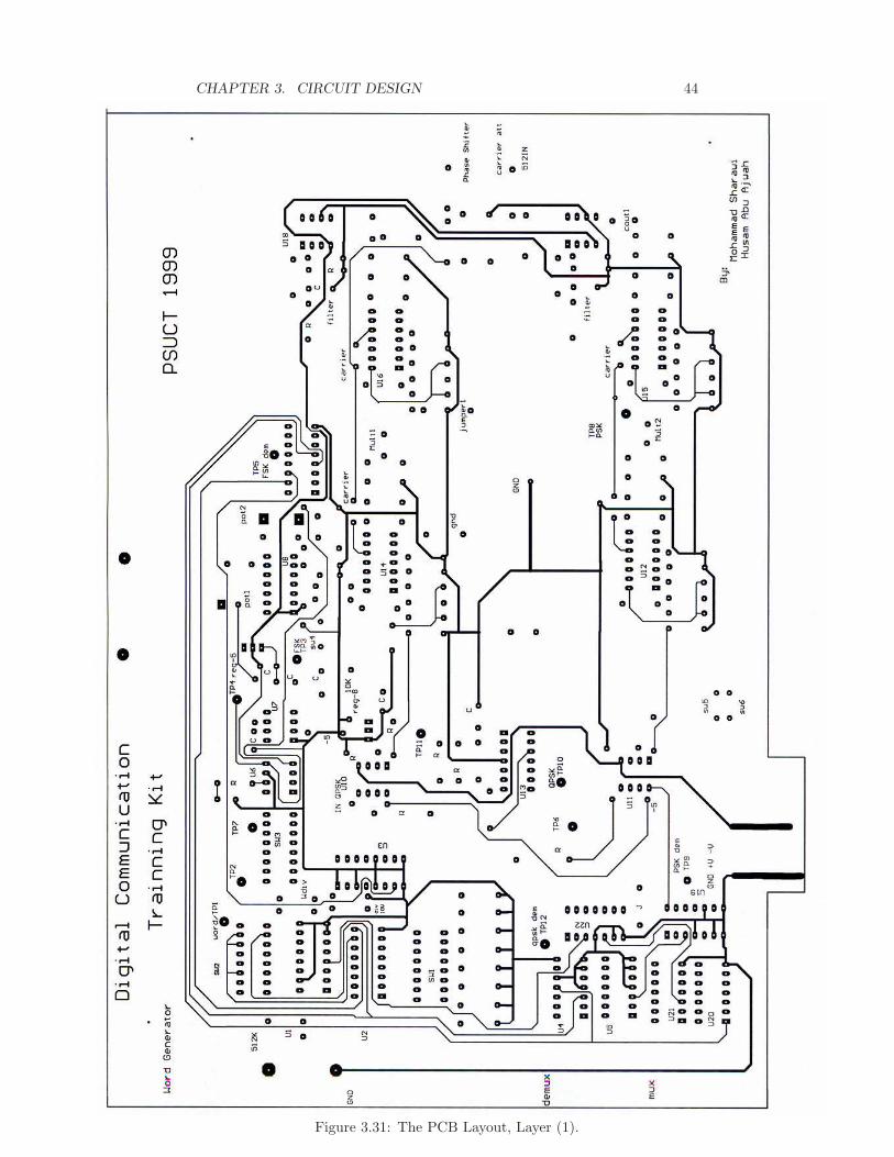
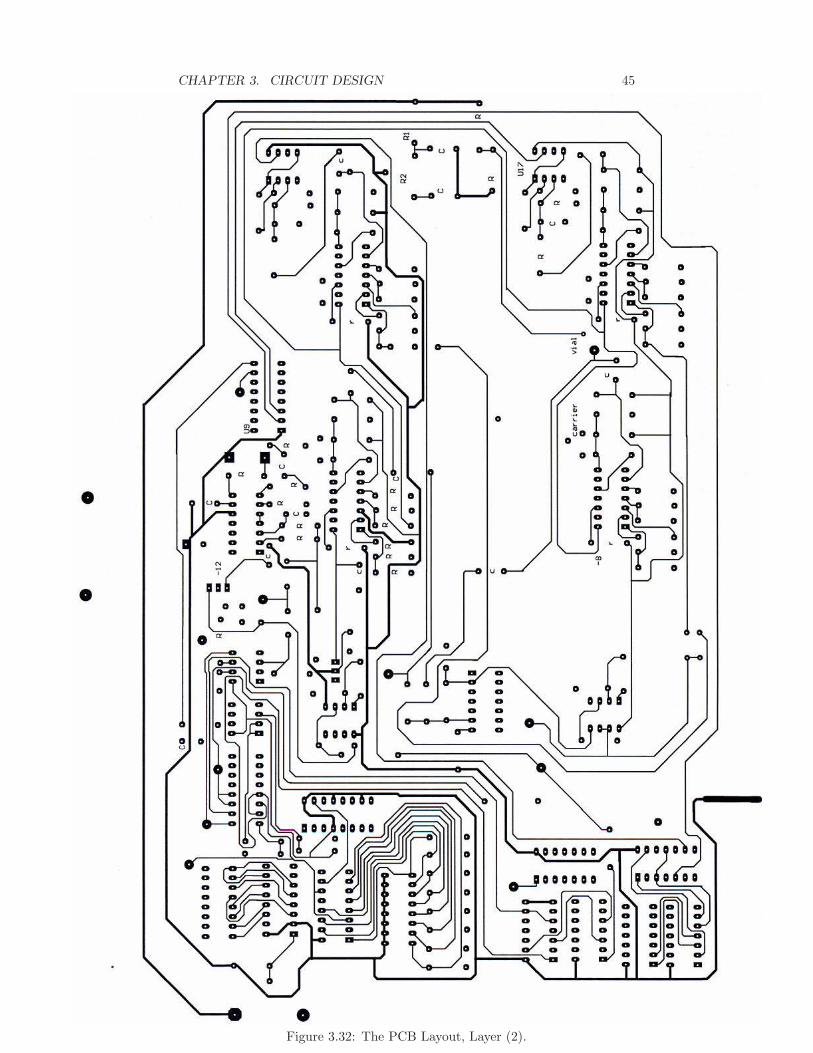
The PCB design was done using a software called PROTEL3 for Windows ver-sion 1.5. Some limitations were taken into consideration such as the size of ourmodule and the position of supply tracks needed for the circuit which are 12V,-12 V and the ground. This is because we had to design our module accordingto the power supply panel base available in the communications lab. Tests weremade to insure this power supply is sufficient for the circuit. We connected ourcircuit to it, same results were obtained. We tried to organize our module in away that each system is in a separate block, 7 sections for 7 major circuits canbe easily noticed. Another thing to mention is that we designed a double sideboard, this is due to the number of ICs and the size we are limited to.
The circuit schematic, circuit layout, and the PCB print out shown in Figures(3.29),(3.30) and (3.31,3.32) respectively will clearly illustrate this.
Switches appears on the schematic are Sw1, Sw2, Sw3, Sw4, Sw5, Sw6.Switches 4,5,6 are for the option of connecting or disconnecting the receivers
of the FSK, the odd, and the even streams respectively from their transmitters.Sw1 is an 8-bit dip switches which determines the word needed to be gener-
ated from the word generator. Sw2 is also an 8-bit dip switch whose outputs arethe clocks generated from the universal clock. These outputs from the left are(2, 4, 8, 16, 256, 128, 64, 32 KHz). Sw3 is a 4-bit dip switches which determineswhich system would operate at the time and disconnects the other systems atthis moment in the following combinations
From Left :
• Up, Down, Down, Down : This would enable the FSK system and discon-nects the PSK input streams.
• Down, Down, Down, Up : This would enable the PSK system (only theodd stream) and disconnects the FSK and the even input streams.
3 c© Protel PCB and Schematic are registered programs for Protel Technologies.

CHAPTER 3. CIRCUIT DESIGN 41
• Down, Up, Up, Down : This would enable the Q-PSK system (odd andeven streams) and disconnects the FSK input stream.
CHAPTER 3. CIRCUIT DESIGN 42
Figure 3.29: The Circuit Schematic of the Module.
CHAPTER 3. CIRCUIT DESIGN 43
Figure 3.30: The Circuit IC and Component Layout.
CHAPTER 3. CIRCUIT DESIGN 44
Figure 3.31: The PCB Layout, Layer (1).
CHAPTER 3. CIRCUIT DESIGN 45
Figure 3.32: The PCB Layout, Layer (2).
Chapter 4
Results
This chapter will demonstrate the final results and output waveforms obtainedfrom the system we designed. This chapter will be divided into three sections,one will illustrate the output signals obtained from the FSK system, the otherfor the PSK, and the final one will demonstrate the QPSK waveforms. Thesegraphs were taken using a Tektronix Digital Oscilloscope.
Results are not included in this report version.For results, please contact the Authors!
46

Chapter 5
Conclusion and Furtherenhancements
5.1 Conclusion
Our project was successfully completed with all the circuits functioning prop-erly. The design demonstrated three of the most common digital modulationtechniques used these days in communications. The circuits were first built andtested on a breadboard, then we designed a PCB and attached the componentsto it. It worked successfully.
Our main aim was to demonstrate these techniques for educational purposes.We think that our design is reliable, and is intended to be used in the digitalcommunication Lab for Educational purposes. That is based on the fact thecircuits were built from commercial ICs that are familiar to all students. Alsothe PCB was designed in a way to be placed on an existing Power Supply basein the lab that is used for other modules, which mean that such a board will beeasily set up in the lab.
The PCB was designed with great care in order to have the least chance ofhaving routing errors that might affect the system performance. Circuit designwith the least amount of components was utilized.
Designing this system involved many thoughts. These included researchingideas, and components, considering simplicity, efficiency, reliability, coast, andsize. We think that the system as a whole was a total success!
5.2 Further Enhancements
Our design was based on the Coherent Detection scheme. That is the carrieris known in advance by the receiver. In real life systems, this is not the case.Non-coherent detection schemes are used in real life receivers. An enhancementon this project is to design non-coherent receivers for the three systems, andto put them on another PCB. This will allow the student to take a broaderlook at the no-ncoherent detection systems and circuit for Digital Modulationtechniques.
One other improvement on this project might be to design an efficient dis-crete multiplier circuit for the PSK and QPSK streams. In the early stages ofour project we were searching and testing the applicability of designing a dis-crete Multiplier circuit. Unfortunately we didn’t have much time to conduct a
47

CHAPTER 5. CONCLUSION AND FURTHER ENHANCEMENTS 48
lot of tests, so we searched for an IC to do the job. This is another enhancementthat might be applicable.
Bibliography
[Bla93] R. Blake. Basic Electronic Communication. West Publishing, secondedition, 1993.
[Bla97] Richard Blahut. Introduction to Telecommunication Theory. Universityof Illinois at Urbana-Champaign, ECE 364 class notes, 1997.
[Bog90] T. F. Bogart. Electronic Devices and Circuits. Merrill Publishing,second edition, 1990.
[EM88] E. I. El-Masri. Analog Filter Design. Technical University of NovaScotia, 1988.
[Fra98] S. J. Franke. Radio Communication Circuits. University of Illinois atUrbana-Champaign, ECE 353 class notes, 1998.
[Hay88] Simon Haykin. Digital Communications. John Wiley and Sons, secondedition, 1988.
[Hay94] Simon Haykin. Communication Systems. John Wiley and Sons, thirdedition, 1994.
[Rap96] Theodore Rapparport. Wireless Communications, Principles and prac-tice. Prentice–Hall Inc., third edition, 1996.
[Raz98] Behzad Razavi. RF Microelectronics. Prentice–Hall Inc., first edition,1998.
[Skl88] Bernard Sklar. Digital Communications, Fundamentals and applica-tions. Prentice–Hall Inc., third edition, 1988.
[SS98] A. Sedra and K. Smith. Microelectronic Circuits. Oxford UniversityPress, third edition, 1998.
49