DIFFERENTIAL CONNECTOR - · PDF fileDIFFERENTIAL CONNECTOR ... LVDS, InfiniBand,10G Ethernet,...
27
1 http://us.fujitsu.com/connectors Specifications subject to change DIFFERENTIAL CONNECTOR FCN-260(D) Series microGiGaCN ™ n SPECIFICATIONS n MATERIALS n FEATURES • I/O Connector designed for high speed differential signal applications. • Matched Impedance (100 ohms ±10%) • Low insertion loss • Low cross talk • Adopted by InfiniBand as 10G Ethernet, SAS, & sATA for 4x/12x Interface m e t I s l a i r e t a M r o t a l u s n I ) 0 - V 4 9 L U ( n i s e R P C L r o t c u d n o C y o l l A r e p p o C g n i t a l P ) S O G A P ( g n i t a l P d l o G : t c a t n o C i N - d P r e v o t a o c d l o G : l a n i m r e T g n i t a l p c n i Z : r e v o C Product Specification are subject to change, please check our website (http://us.fujitsu.com/connectors) for the latest specifications. m e t I s n o i t a c i f i c e p S e r u t a r e p m e t g n i t a r e p O e g n a r C ˚ 5 8 + o t C ˚ 5 5 - g n i t a r t n e r r u C ) l a n g i s ( A 5 . 0 C A ) d n u o r g ( A 1 C A Max. allowable voltage 0 3 C A e c n a t s i s e r t c a t n o C (20m VDC 10mA) ) l a n g i s ( . x a m s m h o m 0 8 d) n u o r g ( . x a m s m h o m 5 4 e c n a t s i s e r n o i t a l u s n I m u m i n i m s m h o M 0 0 0 1 g n i d n a t s h t i w c i r t c e l e i D e g a t l o v e t u n i m 1 r o f V 0 0 5 C A y t i l i b a r u D s e l c y c 0 5 2 e c r o f n o i t r e s n I ) r i a p 8 ( . x a m N 5.5 5 ) r i a p 4 2 ( . x a m N 3 7 e c r o f l w a r d h t i W ) r i a p 8 ( . n i m N 2.5 ) r i a p 4 2 ( . n i m N 8 RoHS Compliant
Transcript of DIFFERENTIAL CONNECTOR - · PDF fileDIFFERENTIAL CONNECTOR ... LVDS, InfiniBand,10G Ethernet,...

1 http://us.fujitsu.com/connectorsSpecifications subject to change
DIFFERENTIAL CONNECTORFCN-260(D) Series microGiGaCN™
n SPECIFICATIONS n MATERIALS
nFEATURES • I/O Connector designed for high speed differential
signal applications. • Matched Impedance (100 ohms ±10%) • Low insertion loss • Low cross talk •AdoptedbyInfiniBandas10GEthernet,SAS,& sATA for 4x/12x Interface
metI slairetaM
rotalusnI )0-V49LU(niseRPCL
rotcudnoC yollAreppoC
gnitalP
)SOGAP(gnitalPdloG:tcatnoCiN-dPrevotaocdloG:lanimreT
gnitalpcniZ:revoC
Product Specification are subject to change, please check our website (http://us.fujitsu.com/connectors) for the latest specifications.
metI snoitacificepS
erutarepmetgnitarepOegnar C˚58+otC˚55-
gnitartnerruC )langis(A5.0CA)dnuorg(A1CA
Max. allowable voltage 03CA
ecnatsisertcatnoC(20m VDC 10mA)
)langis(.xamsmhom08d) nuorg(.xamsmhom54
ecnatsisernoitalusnI muminimsmhoM0001
gnidnatshtiwcirtceleiDegatlov etunim1rofV005CA
ytilibaruD selcyc052
ecrofnoitresnI )riap8(.xamN5.55)riap42(.xamN37
ecroflwardhtiW )riap8(.nimN2.5)riap42(.nimN8
RoHS Compliant
microGiGaCN™ FCN- 260 (D) Series
2 http://us.fujitsu.com/connectorsSpecifications subject to change
TheMicroGigaCNoffersacost-effectiveI/Osolutionforhigh-speedapplicationsindataandtelecommunicationsconvergence(voice,data,videoandstorage).Itoffersfourortwelvelinkwidths,offering a scalable performance range of 500Mbps to6Gbpsperlinktomeettheneedsofentry-levelandhigh-endenterprisesystems.Forwardcrosstalkislessthan4%at100picosecondpulse-risetime(four-pairswitching). FujitsuComponentsdesignedtheMicroGiGaCNtospecificallyaddresstherequirementsforahighspeed differential signal I/O connector.
TheMicroGiGaCNoffersauniquesolutiontoLVDS,InfiniBand,10GEthernet,3G/6GSAS&SATA,andotherhighspeedI/Oapplications.InfiniBand,IEEE802.3ak,SAS,&SATAhaveselectedFujitsu’sconnectorforthe4xand12xI/Oconnector interface. Theperformancerequirementsoftheconnectorsystem were tested with cable to simulate the actual requirementsofanOEMSystemmanufacturer.OurtestdataincludestheparasiticeffectsofthePCB,along with measurements of a completed I/O cable assembly.
• Matched Impedance: 100±10 ohms @ 100 ps Trise
• LowCrossTalk: NEXT4.0%@100pcTrise(20to80%)
• LowInsertionLoss: [email protected](1.25GHz,1meterCableAssembly)
• SkewwithinDifferentialPair: 14.4ps(2connectorsand2meterofcable)
• Skewpairtopair: 21.2ps(2connectorsand2meterofcable)
ElectricalPerformanceinouttesting:
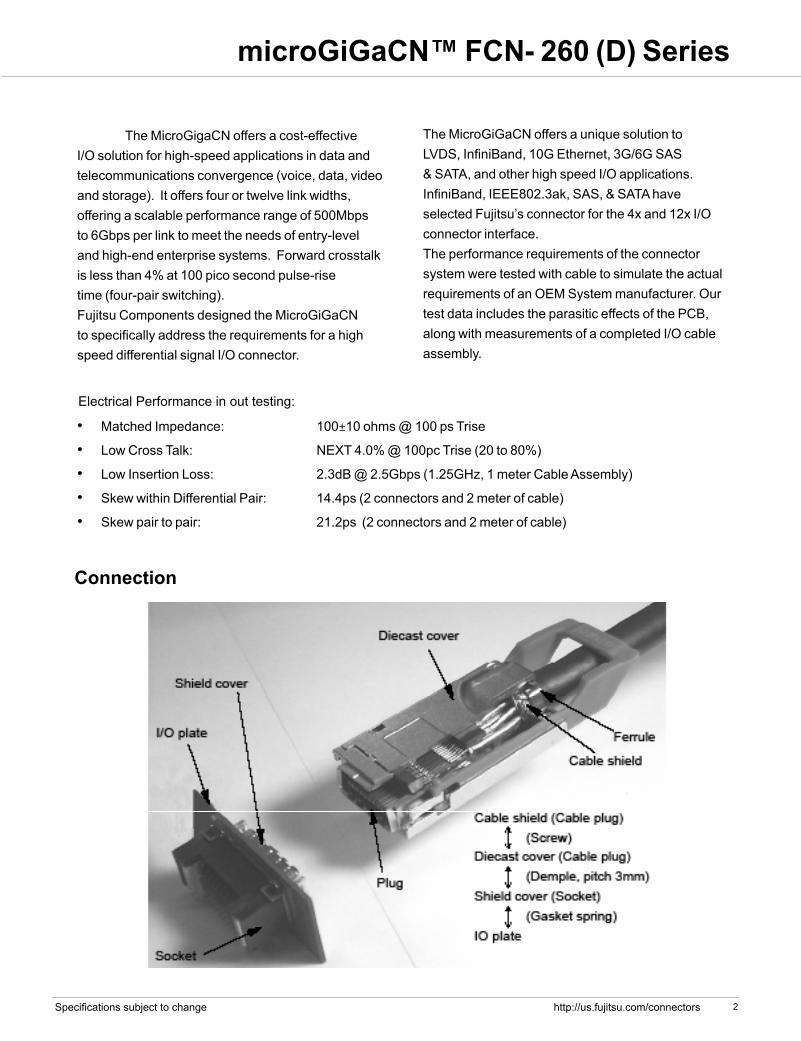
Connection
microGiGaCN™ FCN- 260 (D) Series
3 http://us.fujitsu.com/connectorsSpecifications subject to change
FujitsuComponentshasdesignedthemechanicalfeaturesoftheconnectortoprovidespacesavingfootprintthatwillallowfor34xI/OconnectorstomountontoaPCIform,or212x.AsRFI/EMIarecriticalelementsinhighperformancecableassemblies,FujitsuComponentsprovidesthesurfacemountsocketswithanEMIGroundSpringonthefaceoftheconnector,toinsurethatthemetalsurfaceoftheconnectormakessufficientcontactwiththemetalfaceof the card bracket. The latching mechanism of the backshell offersalanyardsystemforeaseofun-matingtheI/Oplugconnector/cableassemblyfromtheSMTI/Osocket.ThediecastbackshelloffersexcellentRFI/EMIcharacteristics.Thebackshellusesaferruleand
uniquegroundspringsystemtoprovide360degreecontactofthecableshieldtothebackshell,which,combined with the solid interconnect of the socket to faceplate,offerslowACcouplingtermination. ThecurrentversionoftheI/Oplugcomeswith an attached paddlecard for wire termination. Fujitsuoffersthepaddlecardineitheranequalizedorun-equalizedversion(seefactoryfordetailsoftheequalizedversion).Standardproductofferingwillbeun-equalized.Astherearemultipleapplicationsforthepaddlecard,withindustryandcustomerspecificwiretermination,FujitsuComponentsoffersoptionstocustomersofprovidingtheI/Oplugconnectorwithcustom paddlecards (consult factory).
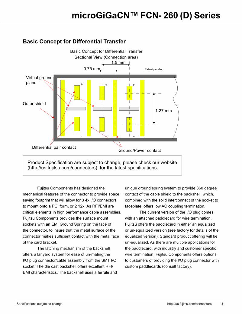
Basic Concept for Differential Transfer
+
-
+
-
1.27 mm
+
-
0.75 mm1.5 mm
Ground/PowercontactDifferential pair contact
Virtual ground plane
SectionalView (Connection area)BasicConceptforDifferential Transfer
Outer shield
Patent pending
ProductSpecificationaresubjecttochange,pleasecheckourwebsite (http://us.fujitsu.com/connectors)forthelatestspecifications.
microGiGaCN™ FCN- 260 (D) Series
4 http://us.fujitsu.com/connectorsSpecifications subject to change
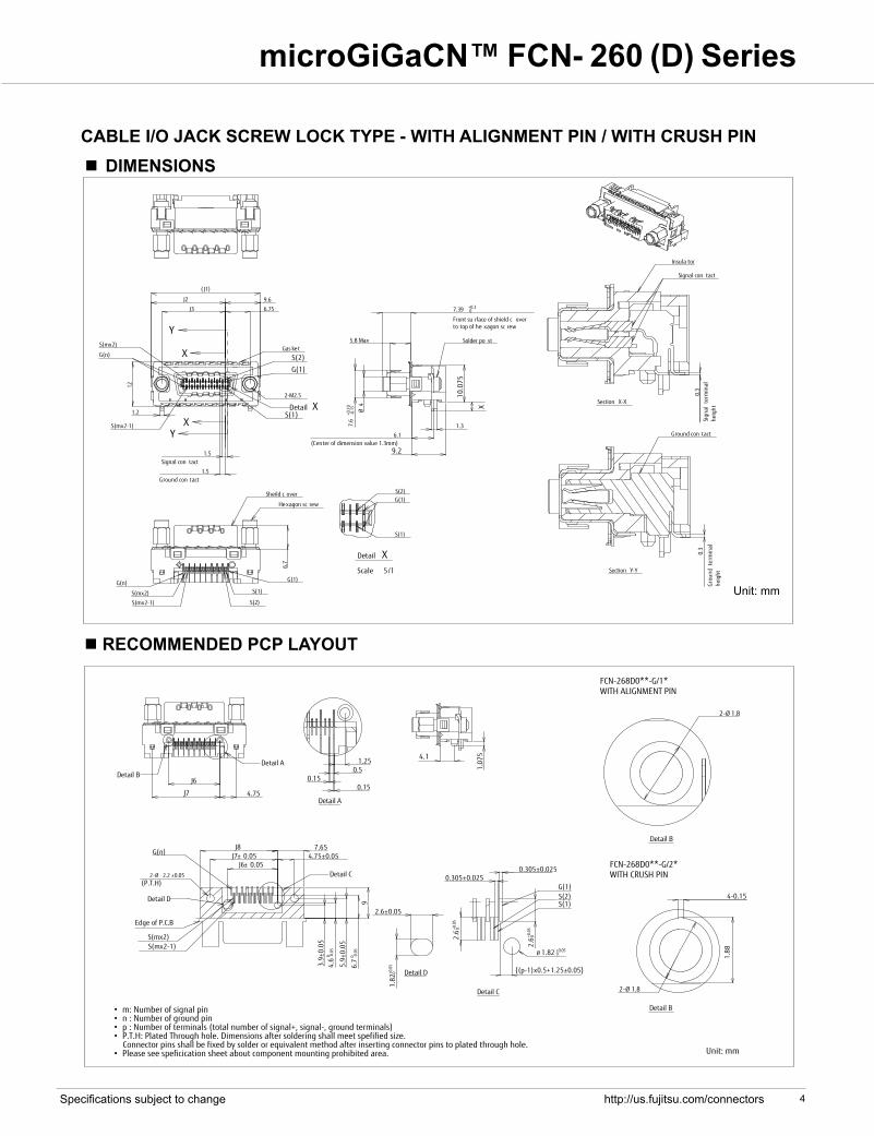
n DIMENSIONSCABLE I/O JACK SCREW LOCK TYPE - WITH ALIGNMENT PIN / WITH CRUSH PIN
Unit: mm
G(1)S(2)
S(1)
Detail XScale 5/1
G(n)
S(mx2)
S(mx2-1)
2-M2.5
Gas ket
Detail XS(1)
G(1)
S(2)
Ground con tact1.5
Signal con tact1.5
6.75J3
12
1.2
( J1)
J2 9.6
X
X
Y
Y
G(1)
S(1)
S(2)S(mx2-1)
S(mx2)
G(n)
Sheild c over
Hexagon sc rew
6.7
Solder po st
Ø4
7.39 +0.3 0
Front su rface of shield c overto top of he xagon sc rew
5.8 Max
(Center of dimension value 1.3mm)6.1
1.3
9.210
.075
X
7.6
+0.1
0-0
.15
Section X-X
Signal con tact
Insula tor
Sign
alte
rmin
alhe
ight
0.3
Section Y-Y
Ground con tact
Gro
und
term
inal
heig
ht
0.3
Detail B
Detail A
Detail B
Detail A
G(n)
Detail C
Detail D
Detail C
G(1)
S(1)S(2)
Detail D
0.5
0.15
0.15
7.65J8
9
0.305 ±0.025
2.6
+0.0
5 0
Ø 1.82 +0.05 0
2.6 ±0.05
1.82
+0.0
5 0
J6
J7 4.75
1.254.1
1.07
5
2-Ø ±0.05
(P.T.H)
2.2
3.9
±0.0
5
4.6
0 -0.0
5
5.9
±0.0
5
6.7
0 -0.0
5
0.305 ±0.025
2.6
+0.0
5 0
2-Ø 1.8
2-Ø 1.8
4-0.15
1.88
Detail B
Detail BJ6
J7
Detail A
4.75
0.15
1.250.5
0.15
Detail A
G(n)
(P.T.H)
Detail D
Edge of P.C.B
S(mx2)S(mx2-1)
J8J7± 0.05 4.75±0.05
J6± 0.05
7.65
Detail C
3.9±
0.05
5.9±
0.05
4.6
6.7
0 -0.0
5
0 -0.0
5
9
+0.0
50
+0.0
50
+0.0
50
+0.050
2.6±0.05
Detail D
1.82
2.6
2.6
Detail C
Ø 1.82
0.305±0.0250.305±0.025
G(1)S(2)S(1)
{(p-1)x0.5+1.25±0.05}
Detail B
Detail B
4-0.15
1.88
4.1
1.07
5
Unit: mm
FCN-268D0**-G/1*WITH ALIGNMENT PIN
FCN-268D0**-G/2*WITH CRUSH PIN
• m: Number of signal pin• n : Number of ground pin• p : Number of terminals (total number of signal+, signal-, ground terminals)• P.T.H: Plated Through hole. Dimensions after soldering shall meet spefified size.
Connector pins shall be fixed by solder or equivalent method after inserting connector pins to plated through hole.• Please see speficication sheet about component mounting prohibited area.
n RECOMMENDED PCP LAYOUT
G(1)S(2)
S(1)
Detail XScale 5/1
G(n)
S(mx2)
S(mx2-1)
2-M2.5
Gas ket
Detail XS(1)
G(1)
S(2)
Ground con tact1.5
Signal con tact1.5
6.75J3
12
1.2
( J1)
J2 9.6
X
X
Y
Y
G(1)
S(1)
S(2)S(mx2-1)
S(mx2)
G(n)
Sheild c over
Hexagon sc rew
6.7
Solder po st
Ø4
7.39 +0.3 0
Front su rface of shield c overto top of he xagon sc rew
5.8 Max
(Center of dimension value 1.3mm)6.1
1.3
9.2
10.0
75
X
7.6
+0.1
0-0
.15
Section X-X
Signal con tact
Insula tor
Sign
alte
rmin
alhe
ight
0.3
Section Y-Y
Ground con tact
Gro
und
term
inal
heig
ht
0.3
Detail B
Detail A
Detail B
Detail A
G(n)
Detail C
Detail D
Detail C
G(1)
S(1)S(2)
Detail D
0.5
0.15
0.15
7.65J8
9
0.305 ±0.025
2.6
+0.0
5 0
Ø 1.82 +0.05 0
2.6 ±0.05
1.82
+0.0
5 0
J6
J7 4.75
1.254.1
1.07
5
2-Ø ±0.05
(P.T.H)
2.2
3.9
±0.0
5
4.6
0 -0.0
5
5.9
±0.0
5
6.7
0 -0.0
5
0.305 ±0.025
2.6
+0.0
5 0
2-Ø 1.8
2-Ø 1.8
4-0.15
1.88
Detail B
Detail BJ6
J7
Detail A
4.75
0.15
1.250.5
0.15
Detail A
G(n)
(P.T.H)
Detail D
Edge of P.C.B
S(mx2)S(mx2-1)
J8J7± 0.05 4.75±0.05
J6± 0.05
7.65
Detail C
3.9±
0.05
5.9±
0.05
4.6
6.7
0 -0.0
5
0 -0.0
5
9
+0.0
50
+0.0
50
+0.0
50
+0.050
2.6±0.05
Detail D
1.82
2.6
2.6
Detail C
Ø 1.82
0.305±0.0250.305±0.025
G(1)S(2)S(1)
{(p-1)x0.5+1.25±0.05}
Detail B
Detail B
4-0.15
1.88
4.1
1.07
5
Unit: mm
FCN-268D0**-G/1*WITH ALIGNMENT PIN
FCN-268D0**-G/2*WITH CRUSH PIN
• m: Number of signal pin• n : Number of ground pin• p : Number of terminals (total number of signal+, signal-, ground terminals)• P.T.H: Plated Through hole. Dimensions after soldering shall meet spefified size.
Connector pins shall be fixed by solder or equivalent method after inserting connector pins to plated through hole.• Please see speficication sheet about component mounting prohibited area.
microGiGaCN™ FCN- 260 (D) Series
5 http://us.fujitsu.com/connectorsSpecifications subject to change
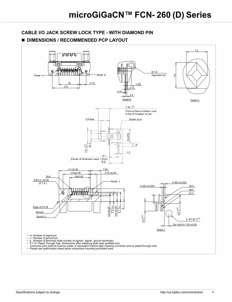
CABLE I/O JACK SCREW LOCK TYPE - WITH DIAMOND PINn DIMENSIONS / RECOMMENDED PCP LAYOUT
1.5
1.8
Detail H
0.150.15
0.5
ØAlignment pin
1.8
1.25
Detail G
Detail J
Edge of P.C.B
S(mx2)
S(mx2-1)
G(n)
9
4.6
0 -0.0
5
3.9
±0.0
5
7.65
J9±0.05
J11±0.05J10±0.05 4.75 ±0.05
2-Ø(P.T.H.)
2.2 ±0.05
6.7
0 -0.0
5
5.9
±0.0
5
Detail GDetail H
J10J9 4.75
G(1)S(2)S(1)
2.6
+0.0
5 0
0.305 ±0.025
2- Ø1.82 +0.05 0
0.305 ±0.025
2.6
+0.0
5 0
{(p-1)x0.5+ ±0.051.25
Detail J
Solder po st
Ø4
7.39 +0.3 0
Front surface of shield c overto top of h exagon sc rew
5.8 Max
(Center of dimension value 1.3mm)6.1
1.3
9.2
10.0
75
X
7.6
+0.1
0-0
.15
• m: Number of signal pin• n : Number of ground pin• p : Number of terminals (total number of signal+, signal-, ground terminals)• P.T.H: Plated Through hole. Dimensions after soldering shall meet spefified size.
Connector pins shall be fixed by solder or equivalent method after inserting connector pins to plated through hole.• Please see speficication sheet about component mounting prohibited area.
microGiGaCN™ FCN- 260 (D) Series
6 http://us.fujitsu.com/connectorsSpecifications subject to change
n DIMENSIONS
CABLE I/O JACK SCREW LOCK TYPEFCN-268D0**-G/ * * PANEL CUTOUT (REFERENCE)
P.C.B
Panel
( )1
( )3.9( )5.9
10.3
±0.1
max
.2.
4
J13±0.1J14±0.1
R m
ax.
0.3
2-Ø3.2+0.05 0
J15±0.1
10° 10°
4.97
5
1.85Unit: mm
n PART NUMBERS
PartNumber
Dimensions (mm)
J13 J14 J15
FCN-264D008-G/** 27 24 19.7FCN-264D024-G/** 51 48 43.7
microGiGaCN™ FCN- 260 (D) Series
7 http://us.fujitsu.com/connectorsSpecifications subject to change
CABLE I/O JACK SCREW LOCK TYPE - WITH ALIGNMENT PIN / WITH CRUSH PIN
n PART NUMBERS FCN-268D**-G/1 with alignment pin
PartNumber PairPCB
thickness (mm)
Dimensions (mm)
X J1 J2 J3 J6 J7 J8
FCN-268D008-G/108
1.6 2.325 29.8 20.15 17.25 14.5 19.25 22.15FCN-268D008-G/11 2.4 3.125 29.8 20.15 17.25 14.5 19.25 22.15FCN-268D008-G/13 4.0 4.725 29.8 20.15 17.25 14.5 19.25 22.15FCN-268D024-G/10
241.6 2.325 53.8 44.15 41.25 38.5 43.25 46.15
FCN-268D024-G/11 2.4 3.125 53.8 44.15 41.25 38.5 43.25 46.15FCN-268D024-G/13 4.0 4.725 53.8 44.15 41.25 38.5 43.25 46.15
n PART NUMBERS FCN-268D**-G/2 with crush pin
PartNumber PairPCB
thickness (mm)
Dimensions (mm)
X J1 J2 J3 J6 J7 J8
FCN-268D008-G/208
1.6 2.325 29.8 20.15 17.25 14.5 19.25 22.15FCN-268D008-G/21 2.4 3.125 29.8 20.15 17.25 14.5 19.25 22.15FCN-268D008-G/23 4.0 4.725 29.8 20.15 17.25 14.5 19.25 22.15FCN-268D024-G/20
241.6 2.325 53.8 44.15 41.25 38.5 43.25 46.15
FCN-268D024-G/21 2.4 3.125 53.8 44.15 41.25 38.5 43.25 46.15FCN-268D024-G/23 4.0 4.725 53.8 44.15 41.25 38.5 43.25 46.15
n PART NUMBERS FCN-268D**-G/3 with diamond pin
PartNumber PairPCB
thickness (mm)
Dimensions (mm)
X J9 J10 J11
FCN-268D008-G/308
1.6 2.325 14.5 19.25 22.15FCN-268D008-G/31 2.4 3.125 14.5 19.25 22.15FCN-268D008-G/33 4.0 4.725 14.5 19.25 22.15FCN-268D024-G/30
241.6 2.325 38.5 43.25 46.15
FCN-268D024-G/31 2.4 3.125 38.5 43.25 46.15FCN-268D024-G/33 4.0 4.725 38.5 43.25 46.15
microGiGaCN™ FCN- 260 (D) Series
8 http://us.fujitsu.com/connectorsSpecifications subject to change
FCN-264D - VERTICAL MOUNT SOCKETS, LATCH STYLEnDIMENSIONS
Unit: mm
n RECOMMENDED PCB LAYOUT (TOP VIEW)
FCN-264D0**-G/1**WITH ALIGNMENT PIN
Section Z-Z(Solder post)
1.2
1.3
1
0.3
Detail V(Signal・Ground Terminal)
S[2]
S[1]
G[1]G[n]
S[2m]
S[2m-1]TYP
Ground Contact Pitch1.5
12
3
A 7.175
TYPSignal Contact Pitch
1.5
X
X
Y
Y
Detail WTYP
Terminal Pitch0.5
6.7
6.4
3.2
2-Ø 1.8
1.25B
C
Detail V
13
0.0251
X
3.9
10.3
4.7
ZZ
Section X-X
Signal contact
Section Y-Y
Ground contact
2-Ø 1.8
2-1.
88
4-R
0.15
2-Ø 1.8
Detail W
(Contact Terminal)
Signal Terminal0.15
Ground Terminal0.15
G[1]
S[2]S[1]
S[2m]
G[n]
S[2m-1]
Connector mounting area
1.25
14+0
.1 0
Ø 1.82+0.05 0
1.82
+0.0
5 0
2.6±0.05
0.305±0.0252-Ø2.2±0.05
3.2±0.05C±0.05
B±0.05
3.9±
0.1
8.8
0 -0.1
1 0 -0.1
{0.5x(p-1)}±0.0
0.5±0.025
(P.T.H)
FCN-264D0**-G/2**WITH CRUSH PIN
• m: Number of signal pin• n : Number of ground pin• p : Number of terminals (total number of signal+, signal-, ground terminals)• P.T.H: Plated Through hole. Dimensions after soldering shall meet specified size
Connector pins shall be fixed by solder or equivalent method after inserting connector pins to plated through hole• Please see speficication sheet about component mounting prohibited area
Unit: mm
microGiGaCN™ FCN- 260 (D) Series
9 http://us.fujitsu.com/connectorsSpecifications subject to change
FCN-264D - VERTICAL MOUNT SOCKETS, LATCH STYLE
n PART NUMBERS FCN-264D**-G/1 with alignment pin
PartNumber PairPCB
thickness (mm)
Dimensions (mm)
X A B C
FCN-264D008-G/1D8
1.6 2.325 17.675 14.5 17.7FCN-264D008-G/1F 2.4 3.125 17.675 14.5 17.7FCN-264D008-G/1K 4.0 4.725 17.675 14.5 17.7FCN-264D024-G/1D
241.6 2.325 41.675 38.5 41.7
FCN-264D024-G/1F 2.4 3.125 41.675 38.5 41.7FCN-264D024-G/1K 4.0 4.725 41.675 38.5 41.7
n PART NUMBERS FCN-264D**-G/2 with crush pin
PartNumber PairPCB
thickness (mm)
Dimensions (mm)
X A B C
FCN-264D008-G/2D8
1.6 2.325 17.675 14.5 17.7FCN-264D008-G/2F 2.4 3.125 17.675 14.5 17.7FCN-264D008-G/2K 4.0 4.725 17.675 14.5 17.7FCN-264D024-G/2D
241.6 2.325 41.675 38.5 41.7
FCN-264D024-G/2F 2.4 3.125 41.675 38.5 41.7FCN-264D024-G/2K 4.0 4.725 41.675 38.5 41.7
n PART NUMBERS
nRECOMMENDED FOOTPRINT DIMENSIONS
Unit: mm
PartNumberDimensions (mm)
RetentionClipPartNumberJ K N
(Panel thickness)P
(Lock plate thickness) K
FCN-264D008-G/** 19.7 22.7 1.0 0.5 6.35 FCN-260A622FCN-264D024-G/** 43.2 46.7 1.0 0.5 6.34 FCN-260A626
I/O Panel
P.C.B.
(F±0
.1)
Thic
knes
s of
I/O
Pane
l
G
Thic
knes
s of
Lock
Pla
te
H±0.1J±0.1
7.2±
0.1
10.3
±0.1
K±0.
2Bo
ard
Surf
ace
to I/
OPa
nel S
urf
ace
4.7
XLe
ngth
of S
olde
rPo
st
Recommended panel thickness = 1±0.1

microGiGaCN™ FCN- 260 (D) Series
10 http://us.fujitsu.com/connectorsSpecifications subject to change
n DIMENSIONS4X / 12X RIGHT ANGLE MOUNT SOCKETS WITH LATCHES
Detail E
Edge of P.C.B.
G[n]
S[2m]
S[2m-1]
Detail F
2- Ø(P.T.H.)
2.2 ±0.05
Detail G(M) (1.575)
( Keep-out area )5.175G ( Keep-out area )9.
73.2 ±0.05
E ±0.05
F ±0.05
5.9
±0.0
56.
7 0 -0
.05
4.6
0 -0.0
5
3.9
±0.0
5
A
Detail D
3.2F571.7A
(B)
E
1.07
5
4.1( )6.1
X
Detail D
0.05 A0.15±0.01
0.05 A0.15 ±0.01
TYP0.5
1.25
S
S
Detail E
Ø (2X)1.8
FCN-268D0**-G/1**WITH ALIGNMENT PIN
Ø (2X)1.8
(2X
)1.
88±0
.05
(4X)0.15
Detail E
FCN-268D0**-G/2**WITH CRUSH PIN
Unit: mm
• m: Number of signal pin• n : Number of ground pin• p : Number of terminals (total number of signal+, signal-, ground terminals)• P.T.H: Plated Through hole. Dimensions after soldering shall meet specified size.
Connector pins shall be fixed by solder or equivalent method after inserting connector pins to plated through hole.• Please see speficication sheet about component mounting prohibited area.
G[1]
S[2]
S[1]
Ø1.82+0.05 0
0.05 A0.305±0.025
0.05 A0.305 ±0.025
TYP0.51.25
A
Detail F
2.6 ±0.05
1.82
+0.0
5 0
S
S
Detail G
Panel
P.C.B.
Panel cutout center line
(N)
(3.9)
(5.9)
(4.75)
(6.75)
7.2±
0.1
10.3
±0.1
K±0.1
J±0.1
R
MAX (8
X).
0.3
4.97
5
P
1.85±0.1 Unit: mm
Recommended panel thickness = 1±0.1
Part NumberDimensions (mm)
Retention CripPart NumberKJ N
(Panel thickness)P
(Lock plate thickness)19.7 22.7 1.0
1.0
0.5
0.5
FCN-260A622FCN-268D008-G/**
FCN-268D024-G/** 43.7 46.7 FCN-260A626PartNumber
Dimensions (mm)RetentionClipPart
NumberJ K N (Panel thickness)
P (Lock plate thickness)
FCN-268D008-G/** 19.7 22.7 1.0 0.5 FCN-260A622FCN-268D024-G/** 43.2 46.7 1.0 0.5 FCN-260A626
n PART NUMBERS
n RECOMMENDED PANEL LAYOUT
microGiGaCN™ FCN- 260 (D) Series
11 http://us.fujitsu.com/connectorsSpecifications subject to change
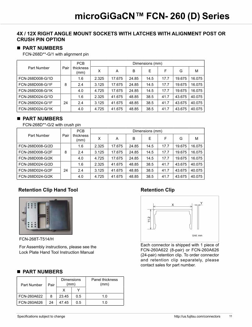
n PART NUMBERS FCN-268D**-G/1 with alignment pin
Eachconnectorisshippedwith1pieceofFCN-260A622 (8-pair) or FCN-260A626(24-pair)retentionclip.Toorderconnectorand retention clip separately, pleasecontact sales for part number.
FCN-268T-T514/H
ForAssemblyinstructions,pleaseseetheLockPlateHandToolInstructionManual
Retention Clip
4X / 12X RIGHT ANGLE MOUNT SOCKETS WITH LATCHES WITH ALIGNMENT POST OR CRUSH PIN OPTION
Retention Clip Hand Tool
n PART NUMBERS
Unit: mm
11.2
X Y
PartNumber PairDimensions
(mm)Panel thickness
(mm)X Y
FCN-260A622 8 23.45 0.5 1.0FCN-260A626 24 47.45 0.5 1.0
PartNumber PairPCB
thickness (mm)
Dimensions (mm)
X A B E F G M
FCN-268D008-G/1D8
1.6 2.325 17.675 24.85 14.5 17.7 19.675 16.075FCN-268D008-G/1F 2.4 3.125 17.675 24.85 14.5 17.7 19.675 16.075FCN-268D008-G/1K 4.0 4.725 17.675 24.85 14.5 17.7 19.675 16.075FCN-268D024-G/1D
241.6 2.325 41.675 48.85 38.5 41.7 43.675 40.075
FCN-268D024-G/1F 2.4 3.125 41.675 48.85 38.5 41.7 43.675 40.075FCN-268D024-G/1K 4.0 4.725 41.675 48.85 38.5 41.7 43.675 40.075
n PART NUMBERS FCN-268D**-G/2 with crush pin
PartNumber PairPCB
thickness (mm)
Dimensions (mm)
X A B E F G M
FCN-268D008-G/2D8
1.6 2.325 17.675 24.85 14.5 17.7 19.675 16.075FCN-268D008-G/2F 2.4 3.125 17.675 24.85 14.5 17.7 19.675 16.075FCN-268D008-G/2K 4.0 4.725 17.675 24.85 14.5 17.7 19.675 16.075FCN-268D024-G/2D
241.6 2.325 41.675 48.85 38.5 41.7 43.675 40.075
FCN-268D024-G/2F 2.4 3.125 41.675 48.85 38.5 41.7 43.675 40.075FCN-268D024-G/2K 4.0 4.725 41.675 48.85 38.5 41.7 43.675 40.075
microGiGaCN™ FCN- 260 (D) Series
12 http://us.fujitsu.com/connectorsSpecifications subject to change
n RECOMMENDED PCB LAYOUT (TOP VIEW)
nDIMENSIONS
4X / 12X RIGHT ANGLE MOUNT CONNECTOR SOCKET WITH LATCHES WITH MOUNTING EARS
C
Detail A
1.8
1.5
S
SDetail C
0.05 A0.15 ±0.01
0.05 A0.15 ±0.01
TYPTerminal pitch0.5
1.25
G1
S1S2
A
B 6.92A
3
TYPGround Contact
1.5
TYPSignal Contact
1.5
2-M2.5
7.2
12.5259.675C
D
12
X
X
Y
Y G1
S1
S2
G(n)
S(mx2)
S(mx2-1)
Section Z-Z(Board pin)
0.1
2 A
1.2
±0.0
5
1.3 ±0.05
1.07
5 X
4.16.19.2
Z Z
Detail B
DetailG(n)
Detail A
Ø 1.8 0-0.05
3.2F
E
6.15
0.3
6.4
±0.1
AS(2xm)
S(mx2-1)
Section X-X
GasketDifferential Signal Contacts
0.3
±0.0
510
.075
Insulator
Section Y-Y
Ground contact
Detail B
Spring0.
33+0
.10
-0.1
5
Section S-S
0.3
60°
Unit: mm
• m: Number of signal pin• n : Number of ground pin• p : Number of terminals (total number of signal+, signal-, ground terminals)• P.T.H: Plated Through hole. Dimensions after soldering shall meet spefified size.
Connector pins shall be fixed by solder or equivalent method after inserting connector pins to plated through hole.• Please see speficication sheet about component mounting prohibited area.
G(n)
S(mx2)
S(mx2-1)
Detail D
Edge of P.C.B. 6.7
0 -0.0
5
5.9±
0.05
0.12 A2-Ø
(P.T.H.)
2.2 ±0.05
4.6
0 -0.0
5
F
3.2
0.1 A2-Ø1.82 +0.05
0
E
3.9±
0.05
1.575
10.525
K
J
9.7
2.6
A
(5.5
5)
LG1
S1S2
Detail D
0.05 A0.305 ±0.025
2.6
+0.0
5 0 2.
6+0
.05
0
0.05 A0.305 ±0.025
TYP0.5
1.25
A
Connector mounting area
Unit: mm
C
Detail A
1.8
1.5
S
SDetail C
0.05 A0.15 ±0.01
0.05 A0.15 ±0.01
TYPTerminal pitch0.5
1.25
G1
S1S2
A
B 6.92A
3
TYPGround Contact
1.5
TYPSignal Contact
1.5
2-M2.5
7.2
12.5259.675C
D
12
X
X
Y
Y G1
S1
S2
G(n)
S(mx2)
S(mx2-1)
Section Z-Z(Board pin)
0.1
2 A
1.2
±0.0
5
1.3 ±0.05
1.07
5 X4.16.19.2
Z Z
Detail B
DetailG(n)
Detail A
Ø 1.8 0-0.05
3.2F
E
6.15
0.3
6.4
±0.1
AS(2xm)
S(mx2-1)
Section X-X
GasketDifferential Signal Contacts
0.3
±0.0
510
.075
Insulator
Section Y-Y
Ground contact
Detail B
Spring
0.33
+0.1
0-0
.15
Section S-S
0.360
°
Unit: mm
• m: Number of signal pin• n : Number of ground pin• p : Number of terminals (total number of signal+, signal-, ground terminals)• P.T.H: Plated Through hole. Dimensions after soldering shall meet spefified size.
Connector pins shall be fixed by solder or equivalent method after inserting connector pins to plated through hole.• Please see speficication sheet about component mounting prohibited area.
G(n)
S(mx2)
S(mx2-1)
Detail D
Edge of P.C.B. 6.7
0 -0.0
5
5.9±
0.05
0.12 A2-Ø
(P.T.H.)
2.2 ±0.05
4.6
0 -0.0
5
F
3.2
0.1 A2-Ø1.82 +0.05
0
E
3.9±
0.05
1.575
10.525
K
J
9.7
2.6
A
(5.5
5)
LG1
S1S2
Detail D
0.05 A0.305 ±0.025
2.6
+0.0
5 0 2.
6+0
.05
0
0.05 A0.305 ±0.025
TYP0.5
1.25
A
Connector mounting area
microGiGaCN™ FCN- 260 (D) Series
13 http://us.fujitsu.com/connectorsSpecifications subject to change
n PART NUMBERS
nRECOMMENDED FOOTPRINT DIMENSIONS
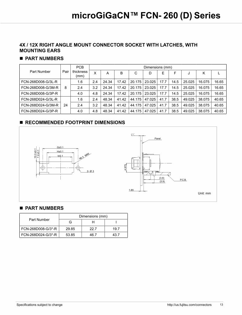
4X / 12X RIGHT ANGLE MOUNT CONNECTOR SOCKET WITH LATCHES, WITH MOUNTING EARS
H±0.1
I±0.17.2
±0.1
10.3
±0.1
R MAX.
0.3
2- Ø 3
G±0.1
Panel
P.C.B.(5.9)
( )1
1.85
(3.9)
4.97
5
PartNumberDimensions (mm)
G H I
FCN-268D008-G/3*-R 29.85 22.7 19.7FCN-268D024-G/3*-R 53.85 46.7 43.7
Unit: mm
n PART NUMBERS
PartNumber PairPCB
thickness (mm)
Dimensions (mm)X A B C D E F J K L
FCN-268D008-G/3L-R8
1.6 2.4 24.34 17.42 20.175 23.025 17.7 14.5 25.025 16.075 16.65FCN-268D008-G/3M-R 2.4 3.2 24.34 17.42 20.175 23.025 17.7 14.5 25.025 16.075 16.65FCN-268D008-G/3P-R 4.0 4.8 24.34 17.42 20.175 23.025 17.7 14.5 25.025 16.075 16.65FCN-268D024-G/3L-R
241.6 2.4 48.34 41.42 44.175 47.025 41.7 38.5 49.025 38.075 40.65
FCN-268D024-G/3M-R 2.4 3.2 48.34 41.42 44.175 47.025 41.7 38.5 49.025 38.075 40.65FCN-268D024-G/3P-R 4.0 4.8 48.34 41.42 44.175 47.025 41.7 38.5 49.025 38.075 40.65

microGiGaCN™ FCN- 260 (D) Series
14 http://us.fujitsu.com/connectorsSpecifications subject to change
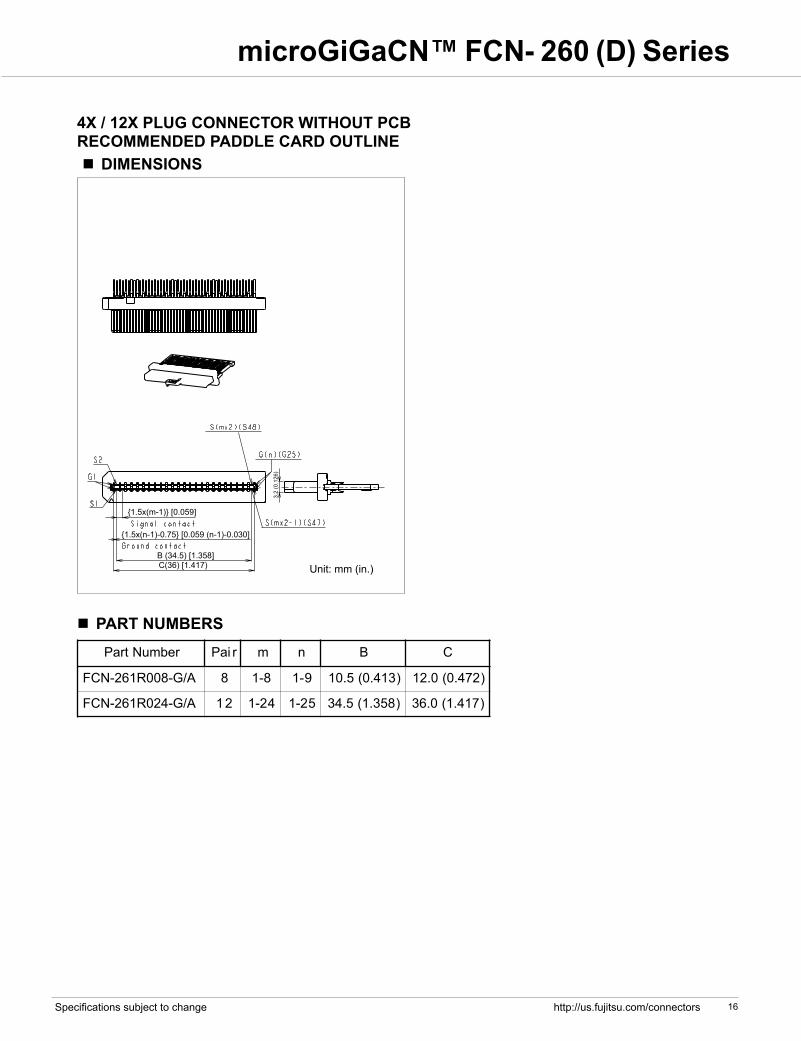
nREFERENCE4X / 12X PLUG CONNECTOR WITH INFINIBAND STYLE PCB
S3S4S7S8
S(2m)S(2m-1)
S2
G1
S1
G(n)S(2m)
S(2m-1){ x(m-1)}
Signal contact1.5
CB
{1.5x(n-1)- }Ground contact
0.75
S2S1S6S5
S(2m-3)S(2m-2)
3.2
(A)
7.9
Slot for guard for miss insertion to cover
Solder pad
()
7.05
()
9.55
18.1
(D)
(E) 0.61.1
0.45
3.04
S(2m)G(n)
S(2m-1)
S2
G1
S1 {1.5 x(m-1)}
{1.5 x(n-1)-0.75}Signal contact
Ground contact
BC
S8S7S4S3
S(2m-1)S(2m)
Unit: mm• m : Number of signal pin • n : Number of ground pin
n PART NUMBERS
PartNumber PairDimensions (mm)
A B C D E
FCN-261R008-G/5L 8 17.7 10.5 12.0 17.4 14.95FCN-261R024-G/5L 24 41.7 34.5 36.0 41.4 38.95

microGiGaCN™ FCN- 260 (D) Series
15 http://us.fujitsu.com/connectorsSpecifications subject to change
n PART NUMBERS4X / 12X PLUG CONNECTOR WITH INFINIBAND STYLE PCB (CABLE MOUNT)
Non-Equalized Plug Kits
Equalized Plug Kits 4x Plug Kits - Equalized
RoHS6/6 DataSpeedsFCN-261R008-G/0L 4xupto3.2Gbps
FCN-261R008-G/5L 4xupto5Gbps
FCN-261R024-G/0L 12xupto3.2GbpsFCN-261R024-G/5L 12xupto5Gbps
RoHS6/6(leadfreesolder) DataSpeeds EqualizedPair
FCN-261R008-G/6L#08 IBDDR8meter,24AWG 1-4
FCN-261R008-G/6L#10 IBDDR10meter,24AWG 1-4
FCN-261R008-G/6L#12 IBDDR12meter,24AWG 1-4
FCN-261R008-G/6M#08 IBDDR8meter,26AWG 1-4
FCN-261R008-G/6M#10 IBDDR10meter,26AWG 1-4
FCN-261R008-G/6M#12 IBDDR12meter,26AWG 1-4
12x Plug Kits - Equalized
RoHS6/6(leadfreesolder) DataSpeeds EqualizedPair
FCN-261R024-G/6L#08 12xIBDDR8meter,24AWG 1-12
FCN-261R024-G/6L#10 12xIBDDR10meter,24AWG 1-12
FCN-261R024-G/6L#12 12xIBDDR12meter,24AWG 1-12
FCN-261R024-G/6M#08 12xIBDDR8meter,26AWG 1-12
FCN-261R024-G/6M#10 12xIBDDR10meter,26AWG 1-12
FCN-261R024-G/6M#12 12xIBDDR12meter,26AWG 1-12
IBSDR=InfiniBandSingleDatarate-2.5Gbps IBDDR=InfiniBandDoubleDatarate-5Gbps Equalizedcircuitsareoptimizedforcablelength/wireAWG
microGiGaCN™ FCN- 260 (D) Series
16 http://us.fujitsu.com/connectorsSpecifications subject to change
n PART NUMBERS
nDIMENSIONS
4X / 12X PLUG CONNECTOR WITHOUT PCBRECOMMENDED PADDLE CARD OUTLINE
Unit: mm (in.)
3.45±0.1(0.136±0.004)
2±0.1(0.079±0.004)
J±0.1(37.95)[1.494]H±0.1(36.5)[1.437]
17±0
.1(0
.669
±0.0
04)
1±0.
1(0.669±0.039)
14.6
±0.1
(0.575±0.039)
G±0.1(38.2)[1.504]1.7±0.1(0.067±0.039)
5.5±
0.1
Pad
cen
ter
(0.2
17±0
.004
)5.
25±0
.1 (0
.507
±0.0
04)
3±0.1(0.120±0.004)
G±0.5(36)[1.417]1.5±0.05 (0.059±0.002)0.75±0.05(0.030±0.002)0.45±0.05 (0.018±0.002)
1.6±
0.1
(0.063±0.004)
1.5±0.05 (0.059±0.002)0.45±0.05(0.018±0.002)
E±0.5(34.5)[1.358]
{1.5x(m-1)}[0.059]
{1.5x(n-1)-0.75}[0.059(n-1)-0.030]
B(34.5)[1.358]C(36)[1.417)
3.2(0.126)
rebmuNtraP riaP m n B C
A/G-800R162-NCF 8 8-1 9-1 )314.0(5.01 )274.0(0.21
A/G-420R162-NCF 21 42-1 52-1 )853.1(5.43 )714.1(0.63
microGiGaCN™ FCN- 260 (D) Series
17 http://us.fujitsu.com/connectorsSpecifications subject to change
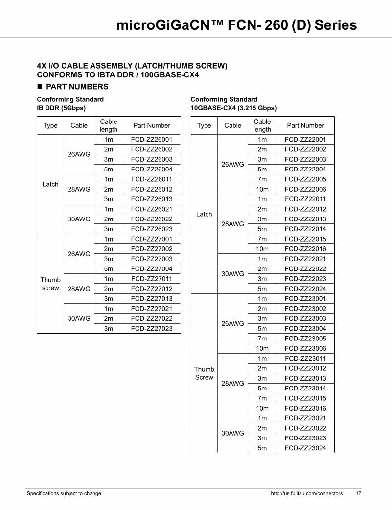
4X I/O CABLE ASSEMBLY (LATCH/THUMB SCREW)CONFORMS TO IBTA DDR / 100GBASE-CX4n PART NUMBERS
Type Cable Cable length PartNumber
Latch
26AWG
1m FCD-ZZ260012m FCD-ZZ260023m FCD-ZZ260035m FCD-ZZ26004
28AWG1m FCD-ZZ260112m FCD-ZZ260123m FCD-ZZ26013
30AWG1m FCD-ZZ260212m FCD-ZZ260223m FCD-ZZ26023
Thumb screw
26AWG
1m FCD-ZZ270012m FCD-ZZ270023m FCD-ZZ270035m FCD-ZZ27004
28AWG1m FCD-ZZ270112m FCD-ZZ270123m FCD-ZZ27013
30AWG1m FCD-ZZ270212m FCD-ZZ270223m FCD-ZZ27023
Type Cable Cable length PartNumber
Latch
26AWG
1m FCD-ZZ220012m FCD-ZZ220023m FCD-ZZ220035m FCD-ZZ220047m FCD-ZZ2200510m FCD-ZZ22006
28AWG
1m FCD-ZZ220112m FCD-ZZ220123m FCD-ZZ220135m FCD-ZZ220147m FCD-ZZ2201510m FCD-ZZ22016
30AWG
1m FCD-ZZ220212m FCD-ZZ220223m FCD-ZZ220235m FCD-ZZ22024
Thumb Screw
26AWG
1m FCD-ZZ230012m FCD-ZZ230023m FCD-ZZ230035m FCD-ZZ230047m FCD-ZZ2300510m FCD-ZZ23006
28AWG
1m FCD-ZZ230112m FCD-ZZ230123m FCD-ZZ230135m FCD-ZZ230147m FCD-ZZ2301510m FCD-ZZ23016
30AWG
1m FCD-ZZ230212m FCD-ZZ230223m FCD-ZZ230235m FCD-ZZ23024
Conforming Standard IB DDR (5Gbps)
Conforming Standard 10GBASE-CX4 (3.215 Gbps)

microGiGaCN™ FCN- 260 (D) Series
18 http://us.fujitsu.com/connectorsSpecifications subject to change
4X I/O CABLE ASSEMBLY (LATCH/THUMB SCREW)CONFORMS TO IBTA DDR / 100GBASE-CX4
nDIMENSIONS LATCH TYPE 4X)
Con
nect
or 1
Labe
l 1
Con
nect
or 2
Labe
l 2
S1
G1
S2 S15
S16
G9
G1
S1
S2
S16
G9
S15
14.4
(71.
9)49
150
±20
150±
20
Fujits
u Co
mpo
nent
Lim
ited
(Lot
.No.
)
Labe
l 2
Insp
ecto
rN
o.
50.8
±5
(Cab
le as
sem
bly p
art n
umbe
r)
Labe
l 1
50.8
±5
micr
oGiG
aCN
TM I/
O
24.9
19.1±5
19.1±5
Unit: mm
microGiGaCN™ FCN- 260 (D) Series
19 http://us.fujitsu.com/connectorsSpecifications subject to change
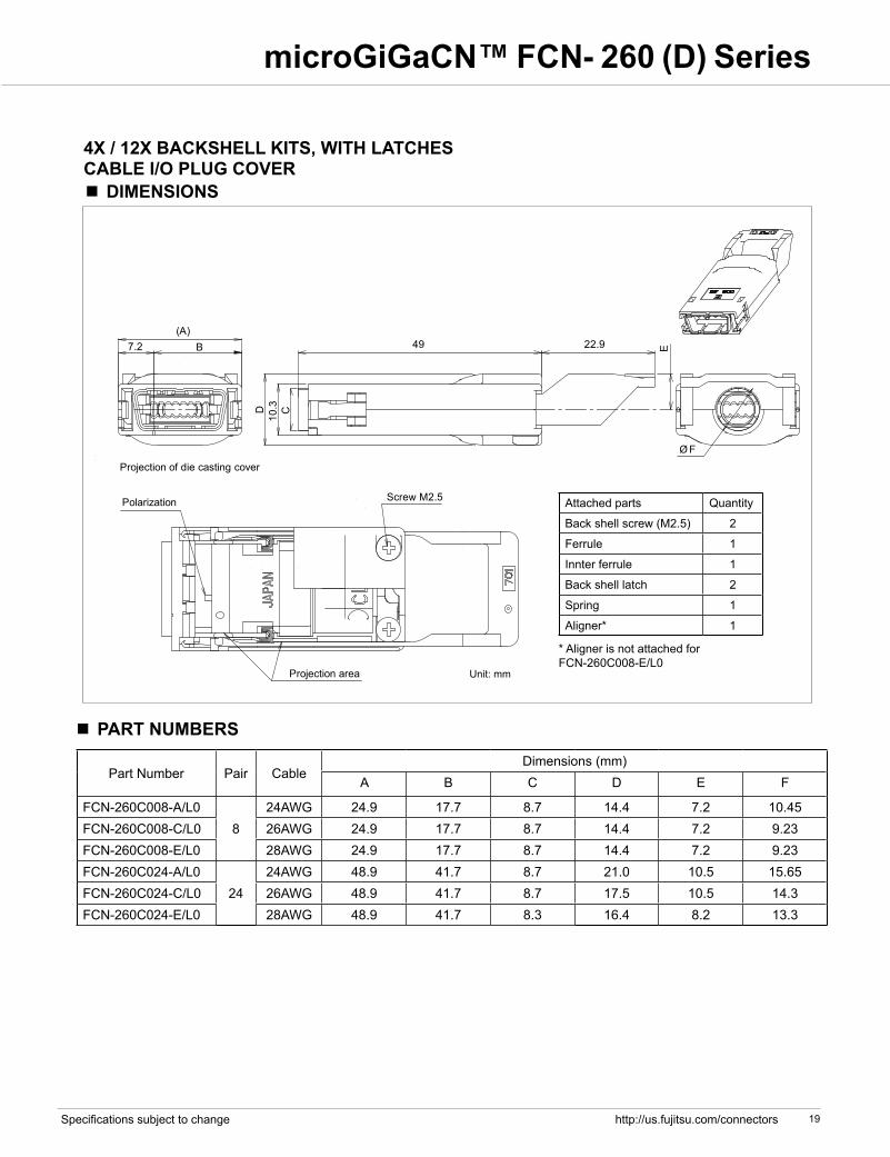
4X / 12X BACKSHELL KITS, WITH LATCHESCABLE I/O PLUG COVER
n PART NUMBERS
nDIMENSIONS
Projection of die casting cover
(A)7.2 B E49 22.9
C10
.3D
Ø F
Screw M2.5Polarization
Projection area Unit: mm
Attached parts Quantity
Backshellscrew(M2.5) 2
Ferrule 1
Innter ferrule 1
Backshelllatch 2
Spring 1
Aligner* 1
*AlignerisnotattachedforFCN-260C008-E/L0
PartNumber Pair CableDimensions (mm)
A B C D E F
FCN-260C008-A/L08
24AWG 24.9 17.7 8.7 14.4 7.2 10.45FCN-260C008-C/L0 26AWG 24.9 17.7 8.7 14.4 7.2 9.23FCN-260C008-E/L0 28AWG 24.9 17.7 8.7 14.4 7.2 9.23FCN-260C024-A/L0
2424AWG 48.9 41.7 8.7 21.0 10.5 15.65
FCN-260C024-C/L0 26AWG 48.9 41.7 8.7 17.5 10.5 14.3FCN-260C024-E/L0 28AWG 48.9 41.7 8.3 16.4 8.2 13.3

microGiGaCN™ FCN- 260 (D) Series
20 http://us.fujitsu.com/connectorsSpecifications subject to change
n DIMENSIONS
4X LOOPBACK MODULE - 8 PAIRSFCN-261Z008 (ROHS 5/6) - discontinued,replacedby:FCN-261Z008L (ROHS 6/6)
17.7 (0.697)
14.4
(0.5
67)
10.3(0.406)
8.7(0.346)
ScrewM2.5
7.2 (0.283)
(24.9)[0.980] 49 (1.929) 22.9 (0.902)
7.2
(0.283)
S2
S1
S47
S48
n DIMENSIONS
12X LOOPBACK MODULE - 24 PAIRSFCN-261Z024 (ROHS 5/6)- discontinued,replacedby:FCN-261Z024L (ROHS 6/6)
7.2(0.283)
41.7 (1.642)
(48.9) [1.925]
21 (0
.827
)
10.3
(0.4
06)
8.3
(0.3
27)
49 (1.929) 20.9 (0.823)
9.61
(0
.039
)
Unit: mm (in.)
Unit: mm (in.)
S2
S1
S15
S16
PinNumber
From To
S1 S16
S2 S15
S3 S14
S4 S13
S5 S12
S6 S11
S7 S10
S8 S9
n PART NUMBERPartNumber PairFCN-261Z008L 8
PinNumber
From To
S1 S48
S2 S47
S3 S46
S4 S45
S5 S44
S6 S43
S7 S42
S8 S41
S9 S40
S10 S39
S11 S38
S12 S37
S13 S36
S14 S35
S15 S34
S16 S33
S17 S32
S18 S31
S19 S30
S20 S29
S21 S28
S22 S27
S23 S26
S24 S25
n PART NUMBERPartNumber PairFCN-261Z024L 24
microGiGaCN™ FCN- 260 (D) Series
21 http://us.fujitsu.com/connectorsSpecifications subject to change
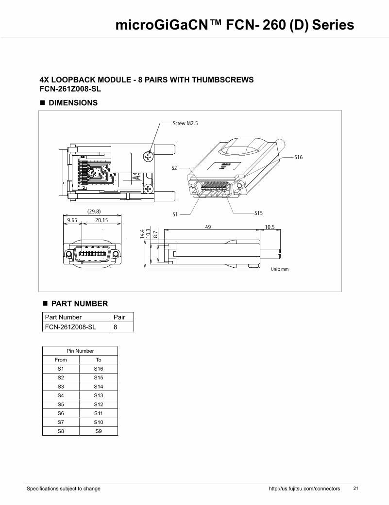
n DIMENSIONS
4X LOOPBACK MODULE - 8 PAIRS WITH THUMBSCREWSFCN-261Z008-SL
n PART NUMBERPartNumber PairFCN-261Z008-SL 8
PinNumber
From To
S1 S16
S2 S15
S3 S14
S4 S13
S5 S12
S6 S11
S7 S10
S8 S9
(29.8)
8.7
10.3
14.4
49 10.5
Screw M2.5
S1
S2
S15
S16
9.65 20.15
Unit: mm

microGiGaCN™ FCN- 260 (D) Series
22 http://us.fujitsu.com/connectorsSpecifications subject to change
n DIMENSIONS4X / 12X BACKSHELL KIT, THUMBSCREWS
n PART NUMBERS
2-M2.5
6.75 C3
Min
.(K
ey s
lot)
7.7
C19.65 C2
K4(Key)K3(Key)
(Key)2.25
1.7 Min.(Key slot width)
(Key)0.75(Key)3.75
K2(Key)K1(Key)
Thumb screw
10.549
C4 10.3
Ø C5
Unit: mm
Attached parts Quantity
Back shell screw (M2.5) 2
2
Ferrule 1
1
1
1
Inner ferrule
Plug key
Spring
Aligner
Thumbscrew
4
PartNumber Pair CableDimmensions (mm)
C1 C2 C3 C4 C5 K1 K2 K3 K4
FCN-260C008-A/S38
24AWG 29.8 20.15 17.25 14.4 10.45 9.75 6.75 5.25 8.25
FCN-260C008-C/S3 26AWG 29.8 20.15 17.25 14.4 9.23 9.75 6.75 5.25 8.25
FCN-260C024-A/S324
24AWG 53.8 44.15 41.25 21.0 15.65 33.75 30.75 29.25 32.25
FCN-260C024-C/S3 26AWG 53.8 44.15 41.25 17.5 14.3 33.75 30.75 29.25 32.25
microGiGaCN™ FCN- 260 (D) Series
23 http://us.fujitsu.com/connectorsSpecifications subject to change
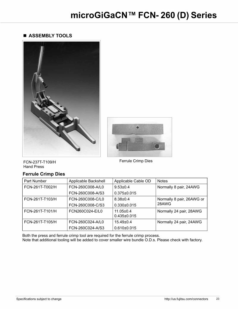
FCN-237T-T109/H HandPress
FerruleCrimpDies
Boththepressandferrulecrimptoolarerequiredfortheferrulecrimpprocess.
Ferrule Crimp Dies
NotethatadditionaltoolingwillbeaddedtocoversmallerwirebundleO.D.s.Pleasecheckwithfactory.
n ASSEMBLY TOOLS
PartNumber ApplicableBackshell Applicable Cable OD NotesFCN-261T-T002/H FCN-260C008-A/L0 9.53±0.4 Normally8pair,24AWG
FCN-260C008-A/S3 0.375±0.015FCN-261T-T103/H FCN-260C008-C/L0 8.38±0.4 Normally8pair,26AWGor
28AWGFCN-260C008-C/S3 0.330±0.015FCN-261T-T101/H FCN260C024-E/L0 11.05±0.4
0.435±0.015Normally24pair,28AWG
FCN-261T-T105/H FCN-260C024-A/L0 15.49±0.4 Normally24pair,24AWGFCN-260C024-A/S3 0.610±0.015
microGiGaCN™ FCN- 260 (D) Series
24 http://us.fujitsu.com/connectorsSpecifications subject to change
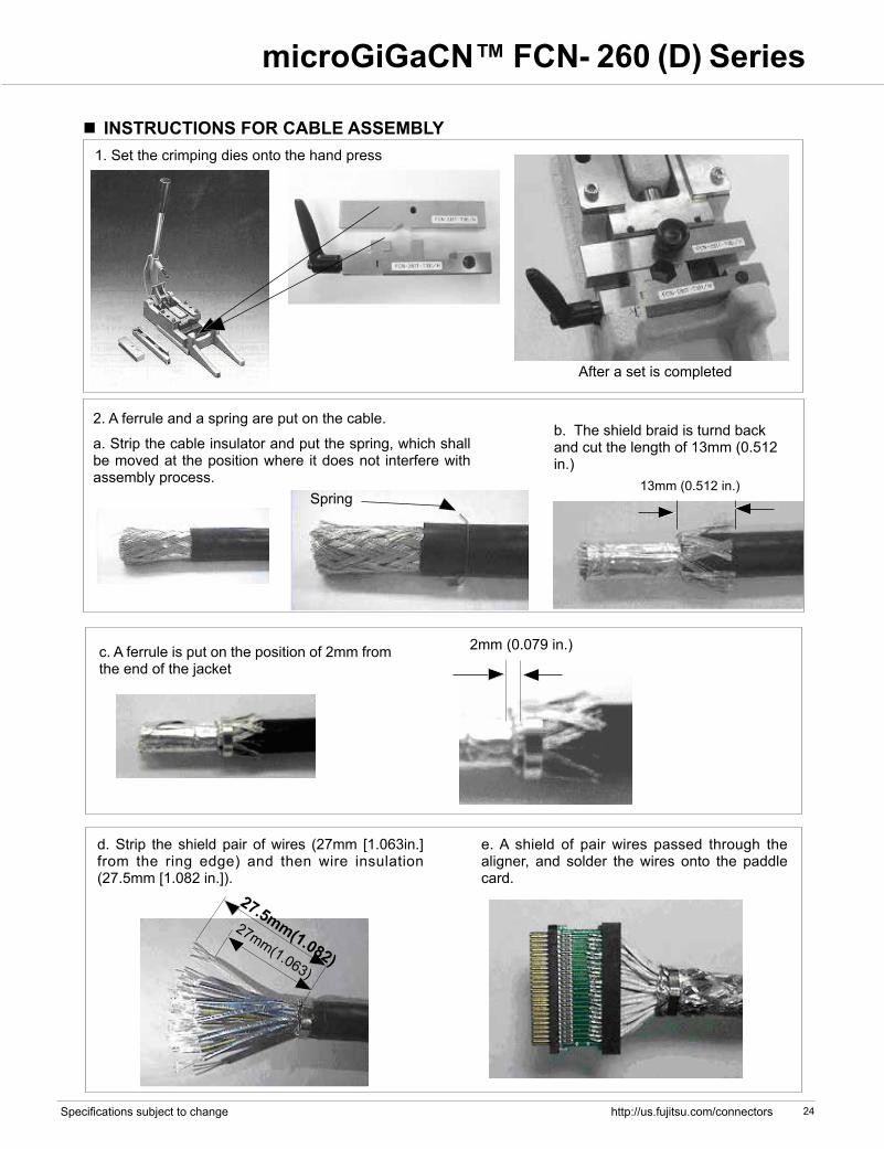
1.Setthecrimpingdiesontothehandpress
n INSTRUCTIONS FOR CABLE ASSEMBLY
2. A ferrule and a spring are put on the cable.
a.Stripthecableinsulatorandputthespring,whichshallbemovedat thepositionwhere itdoesnot interferewithassembly process.
c. A ferrule is put on the position of 2mm from theendofthejacket
e. A shield of pair wires passed through the aligner, and solder thewires onto the paddlecard.
After a set is completed
b. The shield braid is turnd back andcutthelengthof13mm(0.512in.)
d.Strip theshieldpair ofwires (27mm [1.063in.]from the ring edge) and then wire insulation (27.5mm[1.082in.]).
27mm(1.063)
27.5mm(1.082)
Spring13mm(0.512in.)
2mm (0.079 in.)
microGiGaCN™ FCN- 260 (D) Series
25 http://us.fujitsu.com/connectorsSpecifications subject to change
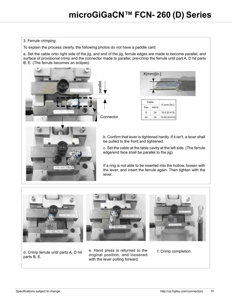
3.Ferrulecrimping:
Toexplaintheprocessclearly,thefollowingphotosdonothaveapaddlecard.
a.Setthecableontorightsideofthejig,andendofthejig,ferruleedgesaremadetobecomeparallel,andsurfaceofprovisionalcrimpandtheconnectormadetoparallel,pre-crimptheferruleuntilpartA,DhitpartsB,E.(Theferrulebecomesaneclipse).
para
llel
Connector
elbaC].ni[)mm(X
riaP GWA
8 42 ]314.0[5.01
42 42 ]416.0[06.51
b.Confirmthatleveristightenedhardly.Ifitisn't,alevershallbe pulled to the front and tightened.
c.Setthecableatthetablecavityattheleftside.(Theferruleedge/endfaceshallbeparalleltothejig).
Ifaringisnotabletobeinsertedintothehollow,loosenwiththelever,andinserttheferruleagain.Thentightenwiththelever.
X(mm)[in.]
d.CrimpferruleuntilpartsA,DhitpartsB,E.
e.Hand press is returned to theoriginal position, and loosenedwiththeleverpullingforward.
f. Crimp completion.

microGiGaCN™ FCN- 260 (D) Series
26 http://us.fujitsu.com/connectorsSpecifications subject to change
Check Y dimension:
Y(mm)[in]
elbaC].ni[)mm(Y
riaP GWA
8 42 ]524.0[8.01
42 42 ]036.0[00.61
4.Turnbackthejacketandcutintheferruleedge.
cut in the ferrule edge
5.Installationofcover:
g.Setthecableandsolderedwiththepaddlecardintotheoutercover.(#1pinpositionsideoftheconnectorshallbeontop)andputanothercover,andsetthespring,whichisinitiallyputonthecable,attheedgeoftheferruleandinstallitinsideandthenfixthecoverswiththescrews.
microGiGaCN™ FCN- 260 (D) Series
27 http://us.fujitsu.com/connectorsSpecifications subject to change
FujitsuComponentsInternationalHeadquarterOfficesContact
Copyright Alltrademarksorregisteredtrademarksarethepropertyoftheirrespectiveowners.FujitsuComponentsAmericaoritsaffiliatesdonotwarrantthatthecontentofdatasheetiserrorfree.InacontinuingefforttoimproveourproductsFujitsuComponentsAmerica,Inc.oritsaffiliatesreservetherighttochangespecifications/datasheetswithoutpriornotice.Copyright©2016FujitsuComponentsAmerica,Inc.Allrightsreserved.RevisedDecmber9,2016
JapanFUJITSUCOMPONENTLIMITEDShinagawaSeasideParkTower12-4,Higashi-shinagawa4-chome,Tokyo1400002,JapanTel:(81-3)3450-1681Fax:(81-3)3474-2385Email:[email protected]:www.fujitsu.com/jp/group/fcl/en/
North and South AmericaFUJITSUCOMPONENTSAMERICA,INC.2290NorthFirstStreet,Suite212 SanJose,CA95131U.S.A.Tel:(1-408)745-4900Fax:(1-408)745-4970Email:[email protected]:http://us.fujitsu.com/components/
EuropeFUJITSUCOMPONENTSEUROPEB.V.Diamantlaan 252132WVHoofddorpNetherlandsTel:(31-23)5560910Fax:(31-23)5560950Email:[email protected]:emea.fujitsu.com/components/
Asia PacificFUJITSUCOMPONENTSASIA,LTD.102EPasirPanjangRoad#01-01CitilinkWarehouseComplex,Singapore118529Tel:(65)6375-8560/Fax:(65)6273-3021Email:[email protected]/sg/products/devices/components/
ChinaFUJITSUELECTRONICCOMPONENTS(SHANGHAI)CO.,LTD.Unit4306,InterContinentalCenter100YuTongRoad,Shanghai200070, ChinaTel:(8621)32530998/Fax:(8621)32530997Email:[email protected]/sg/products/devices/components/
Hong KongFUJITSUCOMPONENTSHONGKONGCO.,LTD.Room06,28/F,GreenfieldTower,ConcordiaPlaza,No.1ScienceMuseumRoad,TsimShaTsuiEast,Kowloon,HongKongTel:(852)28818495Fax:(852)28949512Email:[email protected]/sg/products/devices/components/
KoreaFUJITSUCOMPONENTSKOREA,LTD.AlphaTower#403, 645Sampyeong-dong, Bundang-gu,Seongnam-si,Gyeonggi-do,13524KoreaTel:(8231)708-7108Fax:(8231)709-7108Email:[email protected]/sg/products/devices/components/