Dielectric Nanocomposites with Insulating Propertiesflorin/lab_MEN/doc/Tanaka_v12_n5_2005.pdf ·...
15
T. Tanaka: Dielectric Nanocomposites with Insulating Properties 1070-9878/05/$20.00 © 2005 IEEE 914 Dielectric Nanocomposites with Insulating Properties Toshikatsu Tanaka IPS Graduate School, Waseda University Wakamatsu-ku, Kitakyushu-shi, 808-0135, Japan ABSTRACT Polymer nanocomposites possess promising high performances as engineering materials, if they are prepared and fabricated properly. Some work has been recently done on such polymer nanocomposites as dielectrics and electrical insulation. This was reviewed in 2004 based on the literatures published up to 2003. New significant findings have been added since then. Furthermore, a multi-core model with the far-distance effect, which is closely related to an “interaction zones”, has been proposed from consideration of mesoscopic analysis of electrical and chemical structures of an existing interface with finite thickness. It is speculatively examined in the paper how the model works for various properties and phenomena already found in nanocomposites as dielectrics focusing on electrical characteristics, resistance to high voltage environment, and thermal properties. Index Terms - Nanotechnology, dielectrics, nanocomposites, interfaces, interaction zone, multi-core model. 1 INTRODUCTION Polyamide 6/clay nanocomposite was manufactured as engineering plastics on a commercial basis in 1990. This was a starting point at the engineering level for our interest in polymer nanocomposites. This success initiated research and development efforts to investigate the possibility of combination of various polymers with various nano inorganic fillers. This field is considered to be a descendant of the past consecutive generation of science of colloid, science for interface-activated agents and polymer emulsion, and science and technology of polymer alloys, which could date back to 1910 to 1930, 1950 to 1970, and 1960 to 1980, respectively. Polymer molecular composites and polymer nanocomposites have been a target for R&D since 1970’s. Much effort has been made to develop and apply polymer nanocomposites in transportation, electrical and electronics engineering, food package, and building industries since 1990. In our dielectrics and electrical insulation field, the year 1994 is symbolic, when John Lewis published a paper entitled “Nanometric Dielectrics” in the IEEE Transactions on Dielectrics and Electrical Insulation [1]. Since then, six years had passed until the first experimental data were made public on the nanometric dielectrics in 2002 [2, 3]. Prior to the publications, more detailed concept was made clear to stimulate the investigation of the nanometric dielectrics [4]. Now, we are at dawn for new innovation of solid insulation. Some work has been published with yearly increasing rate since 2002, and group activities have been done in CIGRE as well as in IEEE. The first review was made on manufacturing processes, characterization, and applications of polymer nanocomposites as dielectrics and electrical insulation up to 2003 [5], though they were in the cradle. Further investigation was made to deepen the microscopic understanding of nanodielectrics in general toward future research and development [6, 7]. Polymer nanocomposites are the second generation of what we call filled resins in the insulation engineering, which consist of polymers filled with a large amount (the order of 50 wt%) of micron-sized inorganic fillers. Newly born polymer nanocomposites are defined as a substance of polymers filled with a small amount of nano-fillers. Nano-fillers, even if they are small (few wt%) in content, have a tremendously large surface as compared to micro-fillers. And therefore, it is recognized that it is indispensable to investigate how nano-fillers would interact with polymer matrices for basic understanding of characteristics that emerge due to nanostruturation. Concept of the multi-core model proposed in 2005 would help, which suggests the Manuscript received on 24 January 2005, in final form 24 May 2005.
Transcript of Dielectric Nanocomposites with Insulating Propertiesflorin/lab_MEN/doc/Tanaka_v12_n5_2005.pdf ·...
T. Tanaka: Dielectric Nanocomposites with Insulating Properties
1070-9878/05/$20.00 © 2005 IEEE
914
Dielectric Nanocomposites with Insulating Properties
Toshikatsu Tanaka IPS Graduate School, Waseda University
Wakamatsu-ku, Kitakyushu-shi, 808-0135, Japan
ABSTRACT Polymer nanocomposites possess promising high performances as engineering materials, if they are prepared and fabricated properly. Some work has been recently done on such polymer nanocomposites as dielectrics and electrical insulation. This was reviewed in 2004 based on the literatures published up to 2003. New significant findings have been added since then. Furthermore, a multi-core model with the far-distance effect, which is closely related to an “interaction zones”, has been proposed from consideration of mesoscopic analysis of electrical and chemical structures of an existing interface with finite thickness. It is speculatively examined in the paper how the model works for various properties and phenomena already found in nanocomposites as dielectrics focusing on electrical characteristics, resistance to high voltage environment, and thermal properties.
Index Terms - Nanotechnology, dielectrics, nanocomposites, interfaces, interaction zone, multi-core model.
1 INTRODUCTION
Polyamide 6/clay nanocomposite was manufactured as engineering plastics on a commercial basis in 1990. This was a starting point at the engineering level for our interest in polymer nanocomposites. This success initiated research and development efforts to investigate the possibility of combination of various polymers with various nano inorganic fillers. This field is considered to be a descendant of the past consecutive generation of science of colloid, science for interface-activated agents and polymer emulsion, and science and technology of polymer alloys, which could date back to 1910 to 1930, 1950 to 1970, and 1960 to 1980, respectively. Polymer molecular composites and polymer nanocomposites have been a target for R&D since 1970’s. Much effort has been made to develop and apply polymer nanocomposites in transportation, electrical and electronics engineering, food package, and building industries since 1990.
In our dielectrics and electrical insulation field, the year 1994 is symbolic, when John Lewis published a paper entitled “Nanometric Dielectrics” in the IEEE Transactions on Dielectrics and Electrical Insulation [1]. Since then, six years had passed until the first experimental data were made public on the nanometric
dielectrics in 2002 [2, 3]. Prior to the publications, more detailed concept was made clear to stimulate the investigation of the nanometric dielectrics [4]. Now, we are at dawn for new innovation of solid insulation. Some work has been published with yearly increasing rate since 2002, and group activities have been done in CIGRE as well as in IEEE. The first review was made on manufacturing processes, characterization, and applications of polymer nanocomposites as dielectrics and electrical insulation up to 2003 [5], though they were in the cradle. Further investigation was made to deepen the microscopic understanding of nanodielectrics in general toward future research and development [6, 7].
Polymer nanocomposites are the second generation of what we call filled resins in the insulation engineering, which consist of polymers filled with a large amount (the order of 50 wt%) of micron-sized inorganic fillers. Newly born polymer nanocomposites are defined as a substance of polymers filled with a small amount of nano-fillers. Nano-fillers, even if they are small (few wt%) in content, have a tremendously large surface as compared to micro-fillers. And therefore, it is recognized that it is indispensable to investigate how nano-fillers would interact with polymer matrices for basic understanding of characteristics that emerge due to nanostruturation. Concept of the multi-core model proposed in 2005 would help, which suggests the
Manuscript received on 24 January 2005, in final form 24 May 2005.

IEEE Transactions on Dielectrics and Electrical Insulation Vol. 12, No. 5; October 2005
915
importance of interfaces or interphases between two kinds of materials. This is a model developed from the “interaction zones”. Experimental data are explained in terms of the multi-core model with the far-distance effect.
2 POLYMER NANOCOMPOSITES AS EMERGING ADVANCED MATERIALS
Polymer nanocomposites are newly emerging advanced materials with potential wide application in transportation, electrical and electronics engineering, food packaging, building and other industries [5]. They could be used as high functional materials such as barrier-functional materials, coating materials, flame-retardant materials, foamed materials and the like, as shown Table 1. It should be noted that materials are listed in the order of estimated market demand for high performance materials [8]. Polyolefin is considered most expected in the market, and especially PP is the major material in the polyolefin market. Barrier-functional materials are speculated to account for a largest market share. In order to put their application in reality, steady R&D is needed as shown in Table 2. Table 1. Potential market demand for polymer
nanocomposites. Classification Potential Market Demand High Performance Materials - Transportation Apparatus Parts - Electrical and Electronics Parts - Food Packaging Materials - Building Materials, etc.
Polyeolefin PP, HDPE and others
Other Common Plastics PS and PVC
Engineering Plastics PET, PA, PC, PBT, and Others
Thermoset Resins Epoxy, Phenol and Others
Others PLA, and Others such as
Elastomers and Specialty Resins High Functional Materials
Barrier-Functional Materials PA, PET, EVOH, etc.
Elastomers Base, HDPE Base Coating Materials
Hard Coat Materials
Tribological Materials
WeatheringResistant Materials
Coloring Materials, etc. Foamed Materials Others (with Special Functions)
Polymer nanocomposites are defined as polymers with
a small amount of nano-fillers. They should be called additives by nature rather than fillers, but the word “fillers” is used here, as it might be easily accepted in the insulation field. The nano-fillers are 1 to 100 nm in size, 1 to 10wt% in content, and should be homogeneously
dispersed in the polymer matrix. They can be manufactured by the direct mixing method, the intercalation method, and the sol-gel method that focus the separation of cohesive nano-fillers from each other. Such separation can be obtained by imposing shear force between neighboring nano-fillers or by increasing chemical and or physical intimacy between nano-fillers and their contacting polymer matrix.
Table 2. Major developmental subjects for polymer
nanocomposites. 1 Development of Nanocomposites with Layered Inorganic
Fillers a. Methods to manufacture nanocomposites with perfectly
layer-exfoliated fillers b. Cost reduction in manufacturing methods
2 Development of Nanocomposites based on Common Polymers Especially such as PP, PS, PVC and PET
3 Development of Nanocomposites using Sol-Gel Methods a. Cost reduction in manufacturing methods b. Nanocomposites with a small amount of superfine
nanoparticles
4 Crossover of Nanocomposite Technology with Conventional Technology
5 Development of Nanocomposites with Special Functions
6 Steady Acquisition of Fundamental Data a. Dynamics data b. Structure of compounding machines c. Effect of organic modifiers, dispersants, compatibilizers
and the like d. Reproducibility by proper material processing
Mechanical properties such as tensile strength, impact
strength, elastic modulus, and heat deflection temperature are available as data for various kinds of nanocomposites. Their matrix materials are polyamide (PA), polyolefin [such as polypropylene (PP), polypropylene/maleic anhydride grafted polypropylene (PP/MAPP) blend, ethylene vinyl acetate (EVA) and ethylene vinyl alcohol (EVOH)], polystyrene (PS), polyacrylate and methacrylate, polyethyleneterephthalate (PET), thermoset resin [such as phenol resin, soft epoxy resin, and polyimide (PI)], and others [such as polycarbonate (PC), poly lactic acid (PLA) and ethylene propylene diene methylene linkage rubber (EPDM)]. Layer exfoliatable silicates are major fillers for the above materials, while silica is also used for phenol resin, PI and PC, for instance. Long-term characteristics such as creep, stress relaxation and fatigue, and tribological properties are obtained for some of the materials. Data are partly available for heat resistant properties such as glass transition temperature and crystallization temperature, thermal property such as thermal expansion coefficient, other several characteristics for weathering resistance, water absorption, size stability, transparency and specific gravity. Nanocomposites are expected to hold functional performance such as gas barrier effect, flame retardancy, biodegradability, foaming ability, paint performance and the like, depending on their application.

T. Tanaka: Dielectric Nanocomposites with Insulating Properties 916
Some data are available. Data obtained thus far suggest tentative conclusion as shown in Table 3.
Table 3. Change in material properties due to
nanostructuration by exfoliatable layered silicate. Properties Change in Properties due to
Nanostructuration 1. Mechanical Properties a. Tensile Strength b. Elongation c. Bending Strength d. Elastic Modulus e. Impact Strength f. Tribology g. Creep & Fatigue
Improved. (1.5 to 3 times) Much decreased. (down to almost less than 10 %)
Improve. (1.5 to 3 times) Improved. (2 to 4 times) Not distinct. (Slightly decreased in most cases, 0.7 to 1.3 times)
Improved. Improved.
2. Thermal Properties a. Weight Deflection Temp. b. Melting Point
c. Heat Decomposition Temp.
d. Expansion Coefficient
Improved. (80 to 90 up for crystalline polymers)
(20 to 30 up for amorphous polymers)
Almost unchanged. Improved. Decreased. (down to 1/2)
3. Other Properties a. Weathering Resistance b. Resistance to Chemicals c. Transparency d. Water Absorption e. Size Stability f. Specific Gravity
Not distinct. Unchanged. Unchanged. Improved in some crystalline polymers. Improved. Improved. Almost unchanged.
4. Functional Properties a. Barrier Performance (Impermeability to vapor,
oxygen gas and the like) b. Flame Retardancy c. Biodegradability d. Foaming Property e. Paint Performance f. Other Performances
Improved. (2 to 10 times) Improved. (Especially heat generation rate much decreased)
Not distinct. (Accelerated in some cases) Fine foam makes foamed materials strengthened.
Surface hardness, weathering resistance and the like improved.
Various reports on pigment coloring ability, ion exchange performance, electric and magnetic properties, touch sensors, heat cut performance.
Polymer nanocomposites are expected to emerge in our dielectrics and electrical insulation technology society, as reviewed in 2004 [5]. Much work has been done, since their importance was recognized in 1994 [1], and the first two papers with promising experimental data struck us in 2002 [2, 3]. Polymers such as polyamide (PA), polyethylene (PE), polypropylene (PP), ethylene vinyl acetate (EVA), epoxy resins and silicone rubbers are combined with nano-fillers such as layered silicate (LS), silica (SiO2), titania (TiO2), and alumina (Al2O3). It was found that nano-filler addition has the positive effect on electrical characteristics, resistance to high voltage environment, and thermal endurance.
3 OUTLINE OF THE MULTI-CORE MODEL
The multi-core model of the interface is shown for a spherical inorganic filler particle embedded in a polymer matrix in Figure 1 [9]. It was constructed by the knowledge gained from literature on interfaces [1, 8, 10-31] and interaction zones [3, 20, 32, 34]. It consists of (1) a bonded layer (the first layer) (2) a bound layer (the second layer) (3) a loose layer (the third layer) (4) an electric double layer overlapping the above three
layers
Figure 1. Outline of the multi-core model for polymer
nanocomposites.
The first layer corresponds to a transition layer tightly bonded to both inorganic and organic substances by coupling agents such as silane. The second layer is an interfacial region consisting of polymers chains strongly bound and/or interacted to the first layer and the surface of the inorganic particle. Values of its thickness cited are in the range of 2 to 9 nm. This may correspond to a stoichiomerically crosslinked layer in a certain case. The third layer is a region loosely coupling and interacting to the second layer. It is characterized by different chain conformation, chain mobility, and even free volume or crystallinity from the polymer matrix, which corresponds to a less stoichiomerically crosslinked layer, if any. In addition, an electric double layer such as the Gouy-Chapman diffuse layer is superimposed to form a dipole moment. It is screened by the Debye shielding length up to which charge decays in exponentially with distance according to the Born approximation. Debye shielding length is calculated as 30 nm for example.
The first layer The second layer The third layer Nano-particle
Nearest Neighbor
Matrix 40 to 100 nm
Inter-particle Distance (surface to surface)
Diameter of nano-particle: 20 to 50 nm Thickness of layers: 10 to 30 nm -
-
-
+
+
+
Charge Distribution
Gouy-Chapman Diffuse Layer
Electric Double Layer
Gouy-Chapman diffuse layer will overlap the three layers of the multi-core model.

IEEE Transactions on Dielectrics and Electrical Insulation Vol. 12, No. 5; October 2005
917
4 EXPERIMENTAL RESULTS AND DISCUSSION IN TERMS OF THE
MULTI-CORE MODEL Effects of nanostructuration were summarized in the
reference [5] based on the literature published up to 2003 [10-28], as follow. (1) Direct current (dc) conductivity increases and
decreases depending on measurement conditions. Introduction of deep traps are suggested.
(2) Interfacial polarization can be reduced compared to microcomposites.
(3) There seems to be a certain reduction of permittivity due to nanostructuration. But changes of permittivity as well as tan are complicated, and not conclusive. Manufacturing processes should be more investigated for homogeneous dispersion of nano-fillers.
(4) Space charge, TSC and EL also give complex results in their threshold field and quantity. Introduction of additional levels of shallow and deep traps, as well as increase of trap density, might be involved. These might be deeply related to “interaction zone”. It is therefore necessary to characterize the interaction zones between nano-fillers and polymer matrices chemically and physically.
(5) PD and tracking resistance improve. It is most probable. Role of nano-fillers and interaction zones should be more clarified.
(6) Thermal conductivity and glass transition temperature should be increased by proper methods.
4.1 FREE VOLUME Free volume is discussed to explain the reduction in
permittivity [33]. It is experimentally and theoretically demonstrated that free volume in epoxy titania composite systems will increase when nanostructured, and will decrease when microstructured. The former effect is by +2 to +3 %, whereas the latter one is by -6 to -9 %. The relative free volume is not equal to the relative specific volume according to the calculations. It is proposed that nano-fillers with high energy surface and/or other species are present, which prevent contact between the fillers and the polymer matrices, resulting in the presence of lower density (specific gravity) interlayer. This interlayer can be ascribed to the less stoichiometrically crosslinked layer in the multi-core model. It should be comparatively thick compared to the inner layers to explain reasonable contribution from this layer to free volume and permittivity reduction. In other words, the volume fraction of the outer loose layer is larger than that of the inner bound layer. Two kinds of players are working in the multi-core model to reduce permittivity. The first player, i.e. the inner bound layer (the second layer) acts to impair the motion of dipoles originating from some polar radicals,
and the outer loose layer (the third layer) acts to contribute to the reduction in free volume. Both the layers, if formed, will lead to the reduction of permittivity. The following conditions are required to explain the decrease in permittivity based on the multi-core model.
(i) No or few dipoles and ionic carriers are available in the third layer, nor free to move
(ii) Nano-scale (big size) dipoles induced by the diffuse layer respond to low frequency well below the power frequency.
4.2 PERMITTIVITY
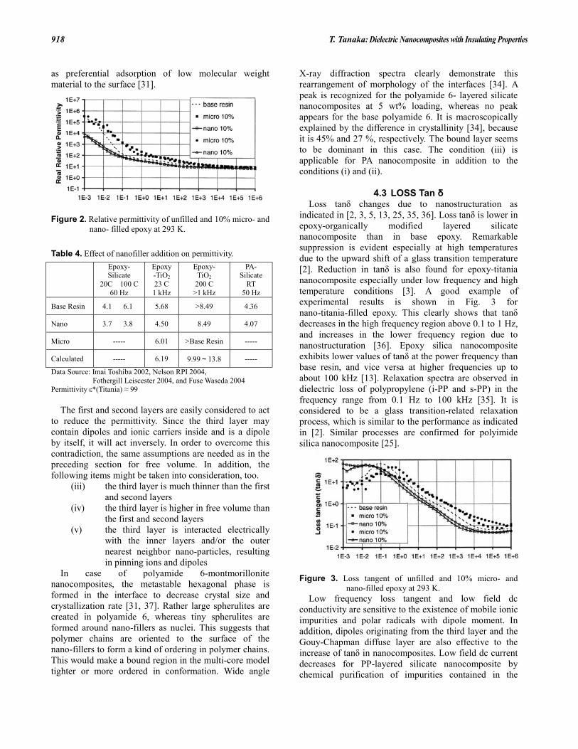
Much work has been made for permittivity study [2, 3, 5, 21, 25, 32, 34-36]. Permittivity usually increases, if polymers are filled with inorganic fillers of micrometer size by several tens wt%. It is because the fillers have higher permittivity by nature than unfilled polymers, and also cause interfacial polarization of the Maxwell-Wagner type. This polarization will naturally increase tan , too. Increased values for micro-composites are usually explained in term of the Lichtenecker-Rother logarithmic law of mixing. Conversely, the permittivity is found to decrease in many cases, if polymers are filled with fillers of nanometer size by several wt%, as typically shown in Fig 2 [36]. Table 4 summarizes the comparison of permittivity among base resins, nanocomposites and microcomposites for several kinds of materials [2, 32-34, 36]. It is clearly demonstrated that all the values cited for the permittivity decrease by nanostruturation. But increased values are also available for what are called nanocomposites. It is possibly due to any accidental inclusion of the imperfection of nanocomposites such as inhomogeneous dispersion and agglomeration of nano-fillers that are technically difficult to avoid, impurities unintentionally mixed in during manufacturing processes, residual curing agents and diluting agents (dispersants) if used.
It is fair to state that the permittivity tends to decrease, if nanostructuration takes place properly. This surprising reduction in permittivity is ascribed to the restriction of polymer chain movement by nano-particles [32]. Some impairment of dipole moment takes place at the interfaces, perhaps resulting from surface hydroxyl (–OH) group bonding. This bonding seems to correspond to the first layer, i.e. a monolayer depicted in the multi-core model. This monolayer with surface hydroxyl (–OH) group bonding would affect the surrounding morphology to form an extended interface (the second and third layers). In the case of epoxy titania nanocomposite, the second layer corresponds to a layer of stoichiometrically crosslinked thermoset with excess curing agent, while the third layer corresponds to a layer of depleted curing agent and thus less stoichiometric crosslinking. And some other changes could occur, such
T. Tanaka: Dielectric Nanocomposites with Insulating Properties 918
as preferential adsorption of low molecular weight material to the surface [31].
Figure 2. Relative permittivity of unfilled and 10% micro- and
nano- filled epoxy at 293 K. Table 4. Effect of nanofiller addition on permittivity.
Epoxy- Silicate
20C 100 C 60 Hz
Epoxy -TiO2
23 C 1 kHz
Epoxy- TiO2
200 C >1 kHz
PA- Silicate
RT 50 Hz
Base Resin 4.1 6.1 5.68 >8.49 4.36
Nano 3.7 3.8 4.50 8.49 4.07
Micro ----- 6.01 >Base Resin -----
Calculated ----- 6.19 9.99 13.8 -----
Data Source: Imai Toshiba 2002, Nelson RPI 2004, Fothergill Leiscester 2004, and Fuse Waseda 2004
Permittivity *(Titania) 99
The first and second layers are easily considered to act to reduce the permittivity. Since the third layer may contain dipoles and ionic carriers inside and is a dipole by itself, it will act inversely. In order to overcome this contradiction, the same assumptions are needed as in the preceding section for free volume. In addition, the following items might be taken into consideration, too.
(iii) the third layer is much thinner than the first and second layers
(iv) the third layer is higher in free volume than the first and second layers
(v) the third layer is interacted electrically with the inner layers and/or the outer nearest neighbor nano-particles, resulting in pinning ions and dipoles
In case of polyamide 6-montmorillonite nanocomposites, the metastable hexagonal phase is formed in the interface to decrease crystal size and crystallization rate [31, 37]. Rather large spherulites are created in polyamide 6, whereas tiny spherulites are formed around nano-fillers as nuclei. This suggests that polymer chains are oriented to the surface of the nano-fillers to form a kind of ordering in polymer chains. This would make a bound region in the multi-core model tighter or more ordered in conformation. Wide angle
X-ray diffraction spectra clearly demonstrate this rearrangement of morphology of the interfaces [34]. A peak is recognized for the polyamide 6- layered silicate nanocomposites at 5 wt% loading, whereas no peak appears for the base polyamide 6. It is macroscopically explained by the difference in crystallinity [34], because it is 45% and 27 %, respectively. The bound layer seems to be dominant in this case. The condition (iii) is applicable for PA nanocomposite in addition to the conditions (i) and (ii).
4.3 LOSS Tan Loss tan changes due to nanostructuration as
indicated in [2, 3, 5, 13, 25, 35, 36]. Loss tan is lower in epoxy-organically modified layered silicate nanocomposite than in base epoxy. Remarkable suppression is evident especially at high temperatures due to the upward shift of a glass transition temperature [2]. Reduction in tan is also found for epoxy-titania nanocomposite especially under low frequency and high temperature conditions [3]. A good example of experimental results is shown in Fig. 3 for nano-titania-filled epoxy. This clearly shows that tan decreases in the high frequency region above 0.1 to 1 Hz, and increases in the lower frequency region due to nanostructuration [36]. Epoxy silica nanocomposite exhibits lower values of tan at the power frequency than base resin, and vice versa at higher frequencies up to about 100 kHz [13]. Relaxation spectra are observed in dielectric loss of polypropylene (i-PP and s-PP) in the frequency range from 0.1 Hz to 100 kHz [35]. It is considered to be a glass transition-related relaxation process, which is similar to the performance as indicated in [2]. Similar processes are confirmed for polyimide silica nanocomposite [25].
Figure 3. Loss tangent of unfilled and 10% micro- and
nano-filled epoxy at 293 K. Low frequency loss tangent and low field dc
conductivity are sensitive to the existence of mobile ionic impurities and polar radicals with dipole moment. In addition, dipoles originating from the third layer and the Gouy-Chapman diffuse layer are also effective to the increase of tan in nanocomposites. Low field dc current decreases for PP-layered silicate nanocomposite by chemical purification of impurities contained in the

IEEE Transactions on Dielectrics and Electrical Insulation Vol. 12, No. 5; October 2005
919
silicate [38]. Conditions (i) (ii) and (iii) are applicable. A charge double layer, if formed, is screened by the Debye shielding length of about 30 nm. A relaxation peak appears at a frequency much below the power frequency.
4.4 LOW FIELD CONDUCTION Nano-filler particles are considered to play a role of
ion scavenger [19], which becomes a possible source of ionic carriers to increase low field conductivity. It was elucidated that such ions could be eliminated by a chemical purification process in EVA and PP layered silicate nanocomposites [38]. This may be related to quasi-conductive regions around nano-particles proposed for epoxy titania and ZnO systems [36]. These phenomena are considered to take place in the third layer of the multi-core model, and to be explained by the percolation among the neighboring third layers. This is closely related to the increase in low frequency permittivity and loss tangent.
4.5 HIGH FIELD CONDUCTION
High field conduction in nanocomposites is treated either by the thermally assisted ionic-hopping current [13, 40] or by the space charge limited current (SCLC) [41], as in conventional polymers. These mechanisms are not specific to nanocomposites. The former is ascribed to polyimide (PI) silica nanocomposites to give the activation energy of 0.68 eV and the hopping distance of 4.3 nm at 10 wt% filler loading. Dependence of absolute values of the conductivity on nano-filler loading is still uncertain. It is stated that the addition of 2 wt% nano-fillers causes a significant reduction in conductivity at 100 and 150 ºC, whereas 10 wt% loading indicates no clear difference.
The latter is discussed for ethylene vinyl acetate (EVA) and isotactic polypropylene (i-PP) – modified organohectorite (layered silicate) nanocomposites to give the trapping depth of 0.6 eV and the time dependent carrier mobility. Threshold electric field strengths are measured for space charge injection and the transition from Ohmic to space charge conduction, and a good agreement is confirmed between the two kinds of parameters for both the materials. This finding gives another evidence for SCLC flow at high field in these nanocomposites. It is suggested from the apparent time-dependent mobility and trap depth that a new structured trap band with distribution is created. It is considered to be shallower than the original trap band relevant to base polymers. Electronic charge carriers will transport in the shallower band to result in larger mobility in nanostructured polymers than in base polymers.
It is suggested that a shallow trap band is introduced [40], as shown in Fig. 4, so that charge carriers have higher mobility, resulting in less space charge accumulated, as experiments clearly show. What happens
to the original traps? There are two possible cases of change in trap distribution, i.e. (i) addition of a new trap distribution to original
traps (ii) replacement of original traps by a new trap
distribution
Figure 4. Transition of trap band to shallower energy level due
to nanostructuration. Addition of a new trap distribution is likely and easy to think. Defects and impurities are likely to be present in the loose layer of low density. Some of them will act as traps. Such traps are likely to be distributed in shallower energy levels than traps originally present in base materials, because this region is low in density, and high in free volume. But this condition of the addition requires the increase in space charge, because deeper traps will trap carriers in the end. On the contrary, space charge reduction is experimentally observed at high electric field [40]. Original traps seem to be replaced by new traps, and then it is reasonable to presume that the original traps are modified by nano-fillers to transform the shallower trap distribution. How could it happen? Interfaces, especially the third layers, can not only accommodate defects, i.e. original traps but also interact with them electrostatically due to the far-distance effect, resulting in pushing them to shallower levels. But which process (i) or (ii) is operative in reality is still questionable.
Threshold field for SCLC is experimentally found to be reduced. This means that a potential barrier at a metal electrode is reduced. What changes for a dielectric-electrode contact? Consider a system consisting of a dielectric (base resin or nanocomposite) and a metal electrode facing in contact each other. Coulomb potential in the dielectric near the electrode should be reduced to explain lowering of threshold for charge injection from the electrode. Height of the Coulomb potential is related to both the electron affinity and the Fermi level. A good image can be made, if both the parameters are increased by a collaborative effect of multi-layered nano-filler particles dispersed in a polymer matrix. But it seems contradictory to the finding that the threshold field for the electro-luminescence inception are
0.81 eV 0.86 eV 0.88 eV 0.92 eV
Conduction Band
Base
Nano
EVA
Nano
Base
i-PP
0.75 eV 0.84 eV 0.89 eV 0.97 eV
Overlap
Shallower trap band

T. Tanaka: Dielectric Nanocomposites with Insulating Properties 920
higher in epoxy titania nanocomposites than in base epoxy and microcomposites [20, 33].
4.6 SPACE CHARGE It is found in epoxy titania, alumina and ZnO
nanocomposites [3, 36], PP and EVA layered silicate nanocomposites [19, 39, 40], and LDPE titania nanocomposite [23] that space charge is mitigated by nanostructuration. Space charge is usually measured by the pulsed electro-acoustic method (PEA method), from which the electric field distribution and then the maximum field can be calculated. Figure 5 shows the dependence of the maximum field on time of voltage application epoxy titania composites, which demonstrate that the maximum field in a micro-filled composite builds up to over twice the average applied field, whereas a nano-filled composite stabilizes at the field just a little bit higher than the average [36]. Trial was made to assign the polarity of charge formed in the composites. Nevertheless, it is not conclusive yet whether charge formed near the electrodes is homo or hetero, because space charge distribution is complicated, and affected by unknown conditions.
Figure 5. Maximum field intensity as a function of voltage
application time in case of epoxy titania microcomposite and nanocomposite.
Charge accumulated in the bulk are considerably large
at the field 60 kV/mm for both EVA and i-PP, but tends to decrease with increasing addition of nano-fillers from 2 to 6 %. Figure 6 shows the dependence of injected charge on applied electric field in base EVA and 6% nano-filled EVA [40]. Similar results are obtained for i-PP, either. A common behavior is that the charge is reduced at high field due to the introduction of nano-fillers, while it is increased at low field. Consequently, the threshold for space charge accumulation shifts to lower values when nano-fillers are introduced, i.e. from 12 to 4 kV/mm and 14 to 5 kV/mm for EVA and i-PP, respectively. It is argued that such charge at low field is ascribed to ionic impurities included in nano-fillers and can be swept away by the pretreatment of nano-filler purification [38].
Figure 6. Space charge threshold characteristics for base EVA
and 6% nano-filled EVA. ODA: synthetic fluoro-hectorite modified by octadecylamine
In summary, the followings are confirmed as the
effects of nanostructuraton: (i) the accumulated charge will reduce (ii) the threshold field will reduce Charge reduction is explained by the introduction of a shallow trap band, and the resulting increase in apparent carrier mobility. Relation between carrier mobility and the multi-core model is discussed in the preceding section 4.5. It is closely related to the loose or diffuse layer of the multi-core model. Threshold reduction can be ascribed to the reduction in the Coulombic barrier near the electrodes that is possible caused by a collective effect of multi-layered nano-filler particles, as discussed in the preceding section, too. But this temporary conclusion seems to be contradictory to the increase in threshold filed for electroluminescence.
4.7 TSC Thermally stimulated current or TSC is measured for
polyimide silica nanocomposite [13, 41], epoxy titania nanocomposite [20]. A TSC peak appears at around 200 ºC for polyimide silica nanocomposite, shifting from 185 ºC for base polyimide [13, 41]. Furthermore, filler content affects the TSC peak to shift in the range of 200 to 220 ºC for 2 to 10 wt%. Introduction of deep traps is suggested for polyimide silica nanocomposite from these findings and measured decrease in electrical conductivity due to nanostructuration. A TSC peak appears at around 130 ºC for epoxy titania nanocomposite, which is ascribed to the release of space charge [20]. It is argued that it is clearly different from the peak (the main chain relaxation) at 90 ºC, and the relaxation peak at 70 ºC. Deep traps seem to be introduced due to nanostructuration, either.
It is likely that the deep traps can be formed in the second layer of the multi-core model for epoxy titania and polyimide silica nanocomposites. It is worthwhile to note that the shallow traps replace the original deep traps

IEEE Transactions on Dielectrics and Electrical Insulation Vol. 12, No. 5; October 2005
921
in EVA and i-PP layered silicate nanocomposites in the third layer of the multi-core model.
4.8 ELECTROLUMINESCENCE It is an experimental observation that EL, i.e.
electroluminescence is suppressed in epoxy titania nanocomposites, while its inception field and response and decay rate increases [20, 32]. The onset field 400 kV/mm of nano-filled epoxy is more than two times that (the field 178 kV/mm) of the micro-filled epoxy and the base resin. Under the application of high field above the EL onset level, light output of the nano-filled epoxy immediately rises to its peak value and then decays over time, while light from the micro-filled resin progressively increases until a steady-state level is attained. On removal of the energization, the light from nano-filled resin disappears within 2 minutes, while that from micro-filled lasts much longer, approximately for 40 minutes. Increase in EL onset field and decrease in EL intensity are ascribed to the likely formation of homo charge near a tip of the electrode, resulting in field mitigation, while fast EL response is attributed to the highly conductive region possibly formed due to overlapping of interaction zones. Homo charge formation is considered to take place macroscopically due to a group effect of multi-layered nano-filler particles which could contribute to the increase in the density of (possibly deep) traps in the second layer of the multi-core model. Furthermore, what is called “the highly conductive region” here may correspond to the third diffuse layer of the multi-core model that can percolate electrically to its nearest neighbors.
4.9 PHOTOLUMINESCENCE Trail was made to identify traps in polypropylene (PP)
by photoluminescence [35]. Fluorescence spectra at 220 – 230 nm were confirmed as the oxidation of the base materials, and it was elucidated that a broad band with its peak at around 450 nm for i-PP originates from maleic anhydrite. No relation of the spectra with traps is clear yet.
4.10 DIELECTRIC BREAKDOWN STRENGTH
Various investigation has been done as shown in the literature [19, 20, 33, 40-44]. It was found that epoxy titania nanocomposite exhibits almost no change in dc short-term breakdown strength up to 10 wt% nano-filler addition at least, while epoxy titania microcomposite shows a big decrease with increasing micro-filler content from zero content [20]. This finding was considered that nanocomposites have a positive effect on breakdown strength as compared to microcomposites. Positive effects of nano-filler loading are also confirmed for i-PP and EVA [19, 40]. Figure 7 shows one of the examples for the effect of nanostructuration on breakdown strength.
Values of the shape parameters in Weibull plots (breakdown strengths at probability 63.2 %) are given as about 360 kV/mm and about 430 kV/mm for i-PP base resin and i-PP-layered silicate nanocomposite with 6 wt% content, respectively, while it remains almost same as about 350 kV/mm for both EVA base resin and EVA-layered silicate nanocomposite with 6 wt% content. It was found, either, by Weibull plot analysis that ac breakdown strength increases with the filler loading percentage from 1 to 10 wt% in PI-alumina and PI-silica nanocomposites as thick as 25 m [41]. Effect of surface chemistry was demonstrated by breakdown strength of LDPE-TiO2 nanocomposites [42]. By using dried nanoscale TiO2, the breakdown strength at the cumulative failure probability of 63.2% was increased by 50% compared with that of the specimens filled by the as-received nanoscale TiO2, close to that of unfilled LDPE. AEAPS (N-(2- aminoethyl) 3-aminopropyl- trimethoxysilane) -coated nanoscale TiO2-filled specimens showed a nearly 40% increase in the breakdown strength compared with that of uncoated, as-received nanosclae TiO2-filled specimens.
Figure 7. Scale and shape parameter values obtained from the
Weibull distribution of breakdown strength.
Treeing experiments are usually carried out to evaluate breakdown strength for mold type insulation. Such experiments carried out for epoxy titania nanocomposite indicate that the values obtained range from about a field of 145 kV/mm (at no loading) to about 170 and 175 kV/mm (10 wt% loading) [32]. It is stated that, at the needle tip field of 100 kV/mm, the extrapolated life of the nanocomposite will be about 10,000 times longer than that of the conventional microcomposite. Epoxy ZnO nanocomposite [43] and epoxy layered silicate nanocomposite [44] also show better performance in ac breakdown strength. It is surprising that the addition of a very small amount (0.5 to 1 wt%) of ZnO nano-particles in epoxy resin can make significant improvement in breakdown time [43]. Weibull plots of breakdown strength for epoxy layered silicate nanocomposite are shown in Figure 8. The statistical analysis clarifies the difference in breakdown strength between the epoxy nanocomposite and a base resin, and shows that the

T. Tanaka: Dielectric Nanocomposites with Insulating Properties 922
former has 10 % higher strength than the latter. Marked difference is confirmed for tree growth between the two materials, too.
Figure 8. Weibull plots of breakdown strength of epoxy base
resin and nanocomposite. It is easy to think that nano-particles become scattering centers for electrons to transport, but it is too big to electrons to scatter. And therefore the other thought is needed for more detailed discussion. Nanocomposites consist of a polymer matrix, a soft layer with lower density (the third layer), a hard layer with higher density (the second layer), a bonded layer (the first layer), and an inorganic particle. Inorganic nano-particles are dispersed in some 10 nm separation and are surrounded by the three layers of the same order of thickness. Electrons are injected via the electrode and/or are produced by collision ionization. Such electrons transport in the composite system, and probably select their path easy to move. The electrons are easiest to move in the region composed of the series of the third layers with large free volume. It is a straightforward conclusion that breakdown strength will be decreased, if the free volume theory is directly taken into consideration. But this is not the case. Electrons can be more accelerated in the regions consisting of the third layers than in other regions. If there are many defects present in this region, they are effective to make a mean free path shorter, resulting in the increase in breakdown strength. Such electrons can be decelerated via collision with the second layer and the defects probably present in the interface between the third layer and the polymer matrix, resulting in the increase in breakdown strength. It should be pointed out that low density cores are not continuous but discrete. Electric double layers around nano-particles can act as Coulombic attraction and repulsion for moving electrons, depending on whether nano-particles are charged positively or negatively. Polarity will be determined by the difference in the electron affinity and the Fermi level. It can be analyzed from the triboelectric series of materials, which is related to triboelectricity and contact charge. Silicone elastomer and polyamide
(PA) tend to be positively charged, while polystyrene (PS), polyethylene (PE), polypropylene (PP) and polytetrafluoroethylene (PTFE) are likely to be negatively charged. No position of charging level is clear for inorganic filler substances such as layered silicate, silica, alumina and titania so that it is not definitely determined whether the polymers are charged positively or negatively, when they are in contact to the fillers. Some suggestion can be drawn from the finding for metallic oxides that charge is distributed in “surface states” with large density to spread under the surface along characteristic distance of about 100 nm [45]. With the above analysis on the possible charge distribution in mind, breakdown processes can be postulated. Electrons are supplied from the negative electrode and/or the Gouy-Chapman diffuse layer, and accelerated by the applied electric field. When electrons move inside the Debye shielding length, they will be scattered or attracted by the Coulomb force to lose the energy they gain from the field. When electrons are outside the Debye shielding length, they are accelerated in a polymer matrix and collide with the third layer or enter inside the Debye shield. In any case, electrons are decelerated to increase breakdown voltage.
Long-term lifetime is extended by nanostructuration in treeing experiments. There are three processes for treeing, i.e. (i) incubation period (ii) tree initiation (iii) tree growth or propagation
Charge injection and extraction processes take place during the incubation period [46, 47]. Charge injection is suppressed by the collaborative effect of nano-filler particles, as described in the preceding subsection 4.6 of space charge, which is a kind of fatigue process. This process will increase tree initiation field, and retard tree initiation time. Enhancement of the dielectric breakdown field will help increase the tree initiation field, too, as discussed above in terms of the multi-core model. If the tree growth is retarded, or the tree propagation is blocked by nano-filler particles, time for treeing breakdown will increase. It is natural to presume that nano-particles surrounded by the three layers act as a barrier against tree propagation. There is a direct experimental observation that electrical trees are blocked by nano-particles and then form zig-zag (tortuous) paths [44]. Trees are initiated at higher electric field in nanocomposites than in base resins, and propagate in the composite system. Such trees may grow easily in the soft region, but not necessarily. Defects are present in this region, too, and may resist to tree growth. Trees, once grown, propagate toward the nano-particles due the local electric field modified by the high permittivity that they possess, and strike the hard cores such as the second layer, the first layer, and even the filler itself.

IEEE Transactions on Dielectrics and Electrical Insulation Vol. 12, No. 5; October 2005
923
For further clarification, it is necessary to combine chemical structure and charge distribution together to gain a full consistent mechanistic image for breakdown.
4.11 PARTIAL DISCHARGE RESISTANCE It was first found in polyamide that partial discharge
resistance or PD resistance is enhanced by transformation from base polyamide (PA) to polyamide layered silicate nanocomposite [5, 17]. Further investigation was carried out to throw light on its mechanism [34, 49, 50]. Surface of polyamide sheets are exposed to partial discharges using the IEC (b) electrode, and evaluated by the surface roughness measured by an AFM (atomic force microscope). One of the typical data is shown in Fig. 9 for the average surface roughness for base PA, PA naocomposite specimens with nano-filler content 2, 4, and 5 wt% as a function of time under ac 6 kV voltage application. This clearly demonstrates that PD resistance is enormously enhanced by nanostructuration.
PD resistance improves in polyimide by nanostructuration with layered silicate [24, 25]. Such a positive effect is confirmed for silicone elastomer nanocomposites with 2 % silica and 5 % layered silicate, either, by the infrared spectroscopy [48]. Radicals such as CH in CH3, CH3-Si-CH3 group, and Si-O-Si group are watched for evaluation. It is recognized that they are greatly reduced by nanostructuration.
For explanation of how PA layered silicate nanocomposite is against PD’s, the following four points are considered as influencing factors [49]. (i) bonding strength between fillers and matrices (ii) inter-filler space or matrix volume surrounded
by neighboring fillers (iii) morphology in the inter-filler space (iv) mesoscopic interaction
In the light of the multi-core model, the first layer can be ascribed to the above (i) item. Ionic bonding is suggested in this case, where the surface organically modified layered silicate is combined to the surrounding PA matrix. Items (ii) and (iii) should be modified into the second and third layers of the multi-core model. The second layer or some ordered structure such as spherulites and crystallites are created around the first layer, which is evident from the WAXA [34], either. The third layer is amorphous more or less, and get in contact to the third layer of the nearest neighbor fillers. A diffuse layer must overlap the three layers. And therefore, these structures might be formed electrochemically by the mesoscopic interaction.
Figure 9. Surface roughness change with time for base
polyamide and nano-filled polyamide subjected to partial discharges.
Remark: NC-2, NC-4 and NC-5: layered silicate content 2, 4 and 5 wt%, respectively.
Detailed analysis is given elsewhere [9]. The second
layer of the multi-core model is considered to be almost adjacent to that of its nearest neighbor filler, and then will occupy almost whole volume of PA layered silicate nanocomposite. If spherulites formed around the filler as the second layer are strong against PD’s compared to the original PA matrix, PA layered silicate nanocomposite becomes PD resistive. PD degradation must start in the amorphous region between the neighboring third layers or the less PD resistant third layer and proceed into the more PD resistant second layer. A same process will go in its next filler environment, as PD’s enter the next the amorphous region, the third layer, and the second layer. Similar discussion can be made for silicone silica and layered silicate nanocomposites, and for polyimide layered silicate nanocomposite, too, on the basis of the multi-core model.
4.12 OUTDOOR INSULATION AND TRACKING Silicone elastomer to be used for outdoor insulators is
expected to have better performances by nanostructuration [21, 48, 51-53]. Flame retardancy improves in silicone elastomer by nanostruturation with layered silicate [21]. PD resistance [48], mechanical properties [51, 52], and material preparation methods [52] are investigated.
No sufficient data are available yet for tracking performances to correlate with the multi-core model. But macroscopically, it would be possible to apply the discussion similar to that for PD resistance on the basis of the multi-core model. It would be suggestive that the third layer of the multi-core model must be predominant compared to the second layer, and this region would resist to tracking.

T. Tanaka: Dielectric Nanocomposites with Insulating Properties 924
4.13 GLASS TRANSITION TEMPERATURE AND THERMAL CONDUCTIVITY
Glass transition temperature decreases or remains unchanged for epoxy by nanostructuration with titania [3], while it increases for epoxy by nanostructuration with layered silicate [2]. Improvement in glass transition temperature must originate from the formation of the second and third layers of the multi-core model. It indicates that fillers and matrices are rather tightly bonded through these layers.
Thermal conductivity enhances for polyimide by nanostructuration with silica [18]. The first layer of the multi-core model is important in this case. This supports the experimental data that coating of fillers helps improve its thermal conductivity. In addition, a collaborative effect among fillers through the second and third layers would work for better thermal conductivity, either.
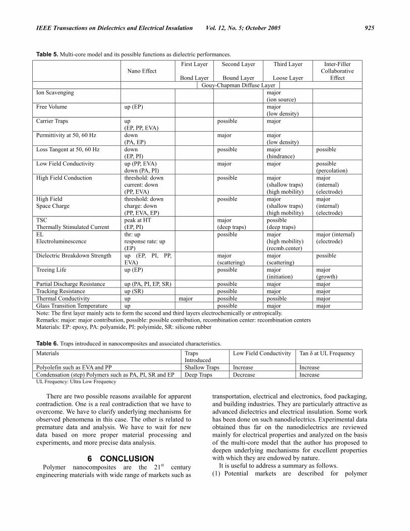
5 DISCUSSION Brief summary is shown in Table 5 as for what
happens in nano-dielectrics, which is drawn from comparison of obtained experimental results with the multi-core model proposed by the author. The multi-core model consists of the first layer (bonded layer), the second layer (bound layer), and the third layer (loose layer). A spherical filler particle is assumed in this model, but any shape will work physically. The Gouy-Chapman diffuse layer overlaps the three layers. Effects of nanostructuration on various kinds of characteristics are briefly described as nano effect. Almost all the characteristics seem to be explained in terms of the second and third layers. Inter-filler collaborative effect is expected to explain some of the phenomena we have encountered. If the inter-filler distance is short enough, an inter-filler interaction will emerge to cause working as collaborative effects. There are at least two functions working as the collaborative effect. Firstly it affects the Coulombic barrier height to change, either increase or decrease depending on conditions, which are related to the electron affinity and/or the Fermi level (electrochemical potential). Secondly it affects carrier transport mechanisms such as their percolation. The first layer of the multi-core model works indirectly for all the characteristics. It acts by nature to create the structures of the second and third layers. It is presumed here that the second and third layers play an important role in characterizing many performances. It would be important to define the role and level of each layer. Ratio of volume fraction and level of influence should be taken into consideration for more detailed discussion.
Many of the data can be successfully explained on the basis of the multi-core model. But some of the data obtained seem to be contradictory, and require further
exploration as a matter of fact. Only three examples are discussed. The first example is shown as follows. Threshold field for space charge formation is reduced in PP and EVA by nanostructuration on one hand. Threshold field for electroluminescence is increased in epoxy resin by nanostructuration on the other hand. Both of the phenomena must be related to charge injection from the electrode. And then it seems to be difficult to explain the two on the basis of the same principle such as the multi-core model. Shallow traps are introduced in PP and EVA, while deep traps are introduced in epoxy resin, as indicated in Table 6. Therefore it is probable to assume that the modification of performances by nanostructuration depends on materials. Different effects will appear on different materials with similar nanostructuration.
A hypothetical explanation is as follows. The second layer plays an important role in epoxy resin, while the third layer does in PP and EVA. In epoxy nanocomposite, the second layer is larger in volume fraction than the third layer, contains deep traps, and cause a collaborative effect through the thin third layer to increase a potential barrier at the electrode. This is related to the electron affinity and Fermi level. In PP and EVA nanocomposites, the third layer is larger in volume fraction than the second layer, contains shallow traps, and causes a collaborative effect to reduce the potential barrier. This image can explain the above phenomena that seem to be contradictory with each other. But further investigation is required. The second problem we have to overcome is the following. Nanostructuration causes the free volume and dielectric breakdown field to increase in epoxy resin at the same time. It is usually understood that the increase in the free volume will make dielectric breakdown field lower. A hypothetical explanation is as follows. The third layer contributes to the increase in the free volume, and to contain a number of scattering centers for electrons to transport. Electrons will be also scattered by the second layer, even if they travel in the third layer easily.
Thirdly we face with a next contradiction as follows. Electroluminescence observed in epoxy resin and depolarization current observed in PP and EVA indicates that there is a conductive zone available for charge carriers. This is ascribed to the third layer of the multi-core model. Existence of the conductive third layer will result in the increase in low field conductivity and tan at ultra-low frequency. In reality, PP and EVA shows an increase in low field conductivity and tan at ultra-low frequency, while PA, PI, silicone rubber and epoxy indicate a decrease in low filed conductivity and an increase in tan at ultra-low frequency. A logical conclusion matches experimental results for PP and EVA, but not those for some condensation polymers.
IEEE Transactions on Dielectrics and Electrical Insulation Vol. 12, No. 5; October 2005
925
Table 5. Multi-core model and its possible functions as dielectric performances.
Nano Effect First Layer
Bond Layer
Second Layer
Bound Layer
Third Layer
Loose Layer
Inter-Filler Collaborative
Effect Gouy-Chapman Diffuse Layer Ion Scavenging major
(ion source)
Free Volume up (EP) major (low density)
Carrier Traps up (EP, PP, EVA)
possible major
Permittivity at 50, 60 Hz down (PA, EP)
major major (low density)
Loss Tangent at 50, 60 Hz down (EP, PI)
possible major (hindrance)
possible
Low Field Conductivity up (PP, EVA) down (PA, PI)
major major possible (percolation)
High Field Conduction threshold: down current: down (PP, EVA)
possible major (shallow traps) (high mobility)
major (internal) (electrode)
High Field Space Charge
threshold: down charge: down (PP, EVA, EP)
possible major (shallow traps) (high mobility)
major (internal) (electrode)
TSC Thermally Stimulated Current
peak at HT (EP, PI)
major (deep traps)
possible (deep traps)
EL Electroluminescence
thr: up response rate: up (EP)
possible major (high mobility) (recmb.center)
major (internal) (electrode)
Dielectric Breakdown Strength up (EP, PI, PP, EVA)
major (scattering)
major (scattering)
possible
Treeing Life up (EP) possible major (initiation)
major (growth)
Partial Discharge Resistance up (PA, PI, EP, SR) possible major major Tracking Resistance up (SR) possible major major Thermal Conductivity up major possible possible major Glass Transition Temperature up possible major major Note: The first layer mainly acts to form the second and third layers electrochemically or entropically. Remarks: major: major contribution, possible: possible contribution, recombination center: recombination centers Materials: EP: epoxy, PA: polyamide, PI: polyimide, SR: silicone rubber Table 6. Traps introduced in nanocomposites and associated characteristics. Materials Traps
Introduced Low Field Conductivity Tan at UL Frequency
Polyolefin such as EVA and PP Shallow Traps Increase Increase Condensation (step) Polymers such as PA, PI, SR and EP Deep Traps Decrease Increase UL Frequency: Ultra Low Frequency
There are two possible reasons available for apparent contradiction. One is a real contradiction that we have to overcome. We have to clarify underlying mechanisms for observed phenomena in this case. The other is related to premature data and analysis. We have to wait for new data based on more proper material processing and experiments, and more precise data analysis.
6 CONCLUSION Polymer nanocomposites are the 21st century
engineering materials with wide range of markets such as
transportation, electrical and electronics, food packaging, and building industries. They are particularly attractive as advanced dielectrics and electrical insulation. Some work has been done on such nanodielectrics. Experimental data obtained thus far on the nanodielectrics are reviewed mainly for electrical properties and analyzed on the basis of the multi-core model that the author has proposed to deepen underlying mechanisms for excellent properties with which they are endowed by nature.
It is useful to address a summary as follows. (1) Potential markets are described for polymer

T. Tanaka: Dielectric Nanocomposites with Insulating Properties 926
nanocomposites based on various kinds of materials. (2) Major developmental subjects are given for polymer
nanocomposites. (3) Change in properties due to nanostructuration is
reviewed. (4) The multi-core model is outlined for polymer
nanocomposites. (5) Various properties are critically reviewed and
explained in terms of the multi-core model. (6) The properties include ion scavenging, free volume,
carrier traps, pemittivity, tan , low field conductivity, high field conduction, thermally stimulated current, electroluminescence, photoluminescence, dielectric breakdown strength, treeing life, partial discharge resistance, tracking resistance, thermal conductivity and glass transition temperature.
(7) The multi-core model consists of the first, second, and third layers, and the multi-core interacts with its nearest neighbors.
(8) The multi-core model can explain many phenomena experimentally observed in connection with the above properties.
(9) There are several contradictions. They are related to the immatureness of the multi-core model, and the incompleteness of material processing and data gathering.
Polymer nanocomposites are promising as near-future dielectrics and electrical insulation from the viewpoint of their inherent excellent properties. First of all, it is requisite to develop suitable not only laboratory-scale but also industrial methods of manufacturing polymer nanocomposites. This will help create reproducible and reliable data to be needed for expanding development of our field. Now, what is basically needed in research is to clarify interfaces between nanoparticles and polymer matrices. Such interfaces certainly depend on the kind of nanoparticle materials, physical and chemical conditions of their surfaces, the kind of coupling agents to bridge inorganic and organic substances chemically and physically, the kind and content of compatibilizers and/or dispersants, and the kind of polymer matrices. They would all determine how a multi-core model is formed as fine structures of interaction zones. Simulation based on advanced computer technology such as molecular dynamics is certainly useful to characterize interfaces and materialize the multi-core model. Sometimes there would be lack in information of manufacturing processes due to confidentiality. This may lead our field to more complexity and difficulty in understanding how good properties would be brought about. To make up this deficiency, too, polymer nanocomposite materials prepared for research should be properly characterized by advanced analytical methods such as wide angle X-ray diffraction (WAXD), small angle X-ray scattering (SAXA), energy dispersive X-ray spectroscopy (EDX), scanning electron microscopy (SEM), field emission
scanning electron microscopy (FE-SEM), transmitting electron microscopy (TEM), and atomic force microscopy (AFM). Dielectric and electrical properties should be correlated with data obtained form such analytical observation. It is also necessary to create a forum for research and promote international cooperation to facilitate and accelerate our research and to put polymer nanocomposites practical as dielectrics and electrical insulation. It will help in R&D, if appropriate demonstration models with polymer nanocomposites such as all solid mini-substation are constructed as common application target.
ACKNOWLEDGEMENT The author acknowledges the financial support for this work by Grants of JPS Basic Research B-14350171, JPS Exploratory Research 16656101, Waseda University RISE Research 04162 and Waseda University Special Subject Research 2004A-328.
REFERENCES [1] T. J. Lewis, “Nanometric Dielectrics”, IEEE Trans. Dielectr.
Electr. Insul. Vol.1, pp. 812-825, 1994.
[2] T. Imai, Y. Hirano, H. Hirai, S. Kojima and T. Shimizu, “Preparation and Properties of Epoxy-Organically Modified Layered Silicate Nanocomposites”, IEEE ISEI, pp. 379-383, 2002.
[3] J. K. Nelson, J. C. Fothergill, L. A. Dissado and W. Peasgood, “Toward an Understanding of Nanometric Dielectrics”, IEEE-CEIDP, pp. 295-298, 2002.
[4] M. F. Fréchette, M. Trudeau, H. D. Alamdari and S. Boily, “Introductory Remarks on NanoDielecttrics”, IEEE-CEIDP, pp. 92-99, 2001.
[5] T. Tanaka, G. C. Montanari and R. Mülhaupt, “Polymer Nanocomposites as Dielectrics and Electrical Insulation –Perspectives for Processing Technologies, Material Characterization and Future Applications”, IEEE Trans. Dielectr. Electr. Insul. Vol. 11, pp. 763-784, 2004.
[6] M. F. Fréchette, M. L. Trudeau, H. D. Alamdari and S. Boily, “Introductory Remarks on Nanodielectrics”, IEEE Trans. Dielectr. Electr. Insul. Vol. 11, pp.808-818, 2004.
[7] M. F. Fréchette, “Reflecting on Material Trends: the Case of Nanodielectrics”, Proc. the 35th Symposium on Electrical and Electronic Insulating Materials and Applications, pp. 25-32, 2004.
[8] K. Chujo, “Polymer Nanocomposites”, Kogyo Chosakai Publishing Inc., pp.1-299, 2003 [in Japanese].
[9] T. Tanaka, M. Kozako, N. Fuse and Y. Ohki, “Proposal of a Multi-core Model for Polymer Nanocomposite Dielectrics”, IEEE Trans. Dielectr. Electr. Insul. Vol. 12, 2005 (In Press).
[10] K. Chujo, Editor, “Advanced Technology and Application of Polymer Nanocomposites”, CMC Press, pp. 1-240, 2001, [in Japanese].
[11] K. Chujo, “Technological Trend in Nano-controlled Composite Materials”, Toray Research Center Library, pp. 1-471, 2002 [in Japanese].

IEEE Transactions on Dielectrics and Electrical Insulation Vol. 12, No. 5; October 2005
927
[12] S. S. Ray and M. Okamoto, “Polymer/layered Silicate Nanocomposites: A Review from Preparation to Processing”, Progress in Polymer Science, Vol. 28, pp.1539-1641, 2003.
[13] Y. Cao and P. C. Irwin, “The Electrical Conduction in Polyimide Nanocomposites”, IEEE-CEIDP, pp.116-119, 2003.
[14] S. S. Sterstein and Ai-Jun Zhu, “Reinforcement Mechanism of Nanofilled Polymer Melts as Elucidated by Non-linear Viscoelastic Behavior”, Macromolecules, Vol. 35, No.5, pp. 7262-7273, 2002.
[15] Yi-Bing Chen, R. J. Varley and G. P. Simon, “Layered Silicate Nanocomposites Based on Various High Functionality Epoxy Resins: The Influence of Cure Temperature on Morphology, Mechanical Properties and Free Volume”, Macromolecules, Vol. 36, pp.1616-1625, 2003.
[16] L.-M. Sun, T. Sakamoto, S. Ueta, K. Koga and M. Takayanagi, “Additive Effects on Thermotropic Liquid Crystal Polymer Alloys I. Effects of Third Component of Thermotropic Liquid Crystal Polymer on Mechanical Properties of Vectra A-Reinforced Polycarbonate”, Polymer J., Vol. 26, pp. 939-952, 1994.
[17] M. Kozako, K. Shibata, N. Hirai, Y. Ohki, T. Okamoto and T. Tanaka, “Surface Change of Polyamide Nanocomposite Caused by Partial Discharges”,. IEEE-CEIDP, pp. 75-78, 2003.
[18] P. C. Irwin, Y. Cao, A. Bansal and L. Schadler, “Thermal and Mechanical Properties of Polyimide Nanocomposites”, IEEE-CEIDP, pp. 120-123, 2003.
[19] C. Zilg, D. Kaempfer, R. Mülhaupt and G. C. Montanari, “Electrical Properties of Polymer Nanocomposites Based upon Organophilic Layered Silicates”, IEEE-CEIDP, pp. 546-550, 2003.
[20] J. K. Nelson and Y. Hu,” Electrical Properties of TiO2 Nanocomposites”, IEEE-CEIDP, pp. 719-722, 2003.
[21] Lei Lan, Xishan Wen, Dengke Cai, Hui Liu, “Study of the Properties of RTV Nanocomposite Coatings”, Proc. 8th ISH (Delft), pp.4, 2003.
[22] Yi Yin, Jiong Chen, Jigning Yang, Dengming Xiao, Demin Tu, Rui Yin and Hongjin Qian, “Effect of Space Charge in Nanocomposite of LDPE/TiO2”, IEEE 7th ICPADM, Nagoya, Japan, pp. 913-916, 2003.
[23] Yi Yin, Jiong Chen, Zhen Liang, Dengming Xiao, Yonghua Zhu, Cao Xu, “The Effect of and Phase Nano Al2O3 on Mechanical Properties of Ethylene-Propylene-Diene Monomer Using in High Voltage Cable Accessories”, Proc. 7th ICPADM (Nagoya), P3-15 , pp.575-578, 2003.
[24] M. Y. Zhang, Chu Yan, Fan Yong and Q. Q. Lei, “Synthesis and Characterization of Corona-resistant Nanocluster-trapped Polyimide/Silica Composites”, IEEE 7th ICPADM, Nagoya, Japan, pp. 753-756, 2003.
[25] Peijong Zhang, Weiguo Zhang, Yan Liu, Yong Fan and Qingquan Lei, “Study on Corona- Resistance of Polyimide-Nano Inorganic Composites”, IEEE 7th ICPADM, Nagoya, Japan, pp. 1138-1141, 2003.
[26] H. Pernot, M. Baumert, F. Court and L. Leibler, “Design and Properties of Co-Continuous Nanostructured Polymers by Reactive Blending”, Nature Materials, Vol. 1, No.1, pp. 54-58, 2002.
[27] Y. Takezawa, M. Akatsuka and C. Farren, “High Thermal Conductive Epoxy Resins with Controlled High Order Structure”, Proc. IEEE-7th ICPADM (Nagoya), pp. 1146-1149, 2003.
[28] Y. Takezawa, “Development of Novel Epoxy Resins Containing Controlled High Order Structure”, Rec. 2004 National Convention of IEE Japan, pp.4, 2004 [in Japanese].
[29] T. J. Lewis, “Interfaces and Nanodielectrics are Synonymous”, IEEE-ICSD, pp.792-795, 2004.
[30] T. J. Lewis, “Interfaces are the Dominant Feature of Dielectrics at the Nanometeric Level”, IEEE Trans. Dielectr. Electr. Insul. Vol. 11, pp.739-753, 2004.
[31] P. M. Ajayan, L. S. Schadler and P. V. Braun, Nanocomposite Science and Technology, Wiley-VCH GmbH & Co. KGaA, pp. 1-230, 2004.
[32] J. K. Nelson and Y. Hu, “The Impact of Nanocomposite Formulations on Electrical Voltage Endurance”, IEEE-ICSD, pp.832-835, 2004.
[33] J. K. Nelson, L. A. Utracki, R. K. MacCrone and C. W. Reed, “Role of the Interface in Determining the Dielectric Properties of Nanocomposites”, IEEE-CEIDP, pp.314-317, 2004.
[34] N. Fuse, M. Kozako, T. Tanaka, S. Murase and Y. Ohki, “Possible Mechanism of Superior Partial-discharge Resistance of Polyamide Nanocomposites”, IEEE-CEIDP, pp.322-325, 2004.
[35] M. Ambid, D. Mary, G. Teyssedre, C. Laurent, G. C. Montanari, D. Kaempfer and R. Mülhaupt, ” Effect of Filler Concentration on Dielectric Behaviour and on Charge Trapping in PP/clay”, IEEE-CEIDP, pp.389-392, 2004.
[36] J. C. Fothergill, J. K. Nelson and M. Fu, “Dielectric Properties of Epoxy Nanocomposites Containing TiO2, Al2O3 and ZnO Fillers”, IEEE-CEIDP, pp.406-409, 2004.
[37] Y. Kojima, A. Usuki, M. Kawasumi, A. Okada, Y. Fukushima, T. Kurauchi and O. Kamigaito, “Mechanical Properties of Nylon-6-Clay Hybrid”, J. Mater. Res. Vol. 8, pp. 1185-1189, 1993.
[38] G. C. Montanari, A. Cavallini, F. Guastavino, G. Coletti, R. Schifani, M. de Lorenzo del Casale, G. Camino and F. Deorsola, “Microscopic and Nanoscopic EVA Composite Investigation: Electrical Properties and Effect of Purification Treatment”, IEEE-CEIDP, pp.318-321, 2004.
[39] G. C. Montanari, G. Teyssedre, C. Laurent, D. Kaempfer and R. Mülhaupt, “Investigating Charge Trapping Behaviour of Nanocomposites with Isotactic and Sydiotactic Polypropylene Matrix”, IEEE-ICSD, pp.836-839, 2004.
[40] G. C. Montanari, D. Faviani, F. Palmieri, D. Kaempfer, R. Thomann and R. Mülhaupt, “Modification of Electrical Properties and Performance of EVA and PP Insulation through Nanostructure by Organophilic Silicates”, IEEE Trans. Dielectr. Electr. Insul. Vol. 11, pp.754-762, 2004.
[41] Y. Cao, P. C. Irwin and K. Younsi, “The Future of Nanodielectrics in the Electrical Power Industry”, IEEE Trans. Dielectr. Electr. Insul. Vol. 11, pp.797-807, 2004.
[42] D. Ma, R. Siegel, J. Hong, L. Schadler: "Influence of Nanoparticle Surfaces on the Electrical Breakdown Strength of Nano-particle-filled Low-Density Polyethylene", J. Mater. Res. Vol.19, pp. 857-863, 2004.
[43] H.-Z. Ding and B. R. Varlow, “Effect of Nano-fillers on Electrical Treeing in Epoxy Resin Subjected to AC Voltage”, IEEE-CEIDP, pp.332-335, 2004.
[44] T. Imai, F. Sawa, T. Yoshimitsu, T. Ozaki and T. Shimizu, “Preparation and Insulation Properties of Epoxy-layered Silicate Nanocomposites”, IEEE-CEIDP, pp.402-405, 2004.

T. Tanaka: Dielectric Nanocomposites with Insulating Properties 928
[45] M. Saint Jean, S. Hudet, C. Guthmann and J. Berger, “Local Triboelectricity on Oxide Surfaces”, Eur. Phys. J. B, Vol. 12, pp. 471-477, 1998.
[46] T. Tanaka, “Space Charge Injected via Interfaces and Tree Initiation in Polymers”, IEEE Trans. Dielectr. Electr. Insul. Vol 8, pp.733-743, 2001.
[47] T. Tanaka and A. Greenwood, “Effects of Charge Injection and Extraction on Tree Initiation in Polyethylene”, IEEE Trans. Power Appr. Syst., Vo. 97, pp.1749-1759, 1978.
[48] L. Lan, X. Wen and D. Cai, “Corona Ageing Tests of RTV Nanocomposite Materials”, IEEE-ICSD, pp.804-807, 2004.
[49] M. Kozako, R. Kido, N. Fuse, Y. Ohki, T. Okamoto and T. Tanaka, “Difference in Surface Degradation due to Partial Discharges between Polyamide Nanocomposites and Microcomposites”, IEEE-CEIDP, pp.398-401, 2004.
[50] M. Kozako, N. Fuse, Y. Ohki, T. Okamoto and T. Tanaka, “Surface Degradation of Polyamide Nanocomposites Caused by Partial Discharges Using IEC (b) Electrode”, IEEE Trans. Dielectr. Electr. Insul., Vol. 11, pp.833-839, 2004.
[51] D. Cai, J. Yu, X. Wen and L. Lan, ”Research on Characterization of RTV Silicone Rubber/LS(Layered Silicate) Electrical Insulation Nanocomposites”, IEEE-ICSD, pp.796-799, 2004.
[52] D. Cai, X. Wen, L. Lan and J. Yu, “Study on RTV Silicone Rubber/SiO2 Electrical Insulating Nanocomposites”, IEEE-ICSD, pp.800-803, 2004.
[53] A. H. El-Hag, S. H. Jayaram and E. A. Cherney, “Comparison between Silicone Rubber Containing Micro- and Nano-size Silica Fillers”, IEEE CEIDP, pp.381-384, 2004. (Related references not cited)
[54] M. Zhang, J. Zhong, K. Zhang and G. Gong, “Preparation and Characterization of the Nano-doped Polyimide Film”, Proc. IEEE-ICSD, pp.840-843, 2004.
[55] M. Kuehn and H. Kliem, “Simulating Nanocomposites using the Methods of Local Fields”, IEEE CEIDP, pp.310-313, 2004.
[56] M. F. Fréchette, R. Y. Larocque, M. Blouin and S. Boily, “Nanophase Semi-conductive Ceramics: Dielectric Surface Performance when Exposed to Charges”, IEEE CEIDP, No. 4-5, pp. 326-331, 2004.
[57] X. Liu, J. L. Spencer, A. B. Kaiser and W. M. Arnold, “Manipulation and Purification of Multiwalled Carbon Nanotubes”, Annu. Rept. IEEE CEIDP, pp.336-339, 2004.
[58] K. Fukushima, H. Takahashi, Y. Takezawa, M. Hattori, M. Itoh and M. Yonekura, “High Thermal Conductive Epoxy Resins with Controlled High-Order Structure”, IEEE CEIDP, pp.340-343, 2004.
[59] N. Bowler, I. J. Youngs, K. P. Lymer and S. Hussain, “Dielectric Relaxation of a Composite with Tungsten Nano-layered Spherical Filler Particles”, IEEE CEIDP, pp.381-384, 2004.
[60] M. F. Fréchette, R. Y. Larocque, R. Viellette and M. L. Trudeau, “Meso and Nano Morphological Changes of an Epoxy Surface Exposed to Low-intensity Discharges in Air”, IEEE CEIDP, pp.393-397, 2004.
[61] T. Imai, F. Sawa, T. Ozaki, T. Nakano, T. Shimizu and T. Yoshimitsu, “Preparation and Insulation Properties of Epoxy-Layered Silicate Nanocomposite”, IEEJ Trans. A, Vol. A-124, No. 11, pp.1064-1072, 2004 [in Japanese].
[62] M. Iwamoto, T. Manaka and O-Y. Zhongcan, “Monolayer Dielectrics and Generation Maxwell-displacement Current and Optical Second Harmonics”, IEEE Trans. Dielectr. Electr. Insul. Vol. 11, pp.785-796, 2004.
[63] C. Brosseau and P. Talbot, “Effective Permittivity of Nanocomposite Powder Compacts”, IEEE Trans. Dielectr. Electr. Insul., Vol. 11, pp.819-832, 2004.
Toshikatsu Tanaka (SM’95-F’00) is
Professor at IPS Graduate School, Waseda University. He was born in Tokyo, Japan in 1939. He received the M.Sc. and Ph.D. degrees in materials science from Osaka University, Japan, in 1964 and 1968, respectively. He served as Vice President at CRIEPI (Central Research Institute of Electric Power Industry) from 1995 to 2001, where he had worked for 37 years since 1964. He was Visiting Lecturer at Salford
University, UK from 1970 to 1972, Visiting Associate Professor at Rensselaer Polytechnic Institute and Visiting Scientist at General Electric Corporate Research, USA from 1975 to 1976. He was also Visiting Professor at Kyushu University, Japan from 1993 to 1997. His interest has covered electrical properties of polymers, dielectric failure and aging mechanisms of polymers, superconducting technologies, laser-induced lightning, fuel cells, lithium secondary batteries, energy storage in electric power systems. He is a recipient of IEEJ A-Society Award 2001, IEEJ 2001 Professor Inuishi Award, IEEE DEIS 2001 Whitehead Award, Minister of Science and Technology Prize 2000, IEE Japan Award 1995, IEE Japan Technology Progress Award 1988, IEE Japan Award for Excellent Book 1985 and IEE Japan Excellent Paper Awards in 1983 and 1970. Dr. Tanaka is a Member of CIGRE, Member of New York Academy, Senior Member of IEE of Japan, Member of Physical Society of Japan, Member of Institute of Cryogenic Society of Japan, Member of Research Association of Superconducting Magnetic Energy Storage, Member of Japan Society of Energy and Resources and an Associate Editor of IEEE Transactions on Dielectrics and Electrical Insulation.