Diamond Particle Detectors for High Energy Physics · Keywords: Particle detectors, radiation...
6
Diamond Particle Detectors for High Energy Physics William Trischuk Department of Physics, University of Toronto, 60 Saint George St., Toronto, Ontario, Canada On behalf of the RD42 Collaboration – see Appendix A Abstract Diamond devices have now become ubiquitous in the LHC experiments, finding applications in beam background monitoring and luminosity measuring systems. This sensor material is now maturing to the point that the large pads in existing diamond detectors are being replaced by highly granular tracking devices, in both pixel and strip configurations, for detector systems that will be used in Run II at the LHC and beyond. The RD42 collaboration has continued to seek out additional diamond manufacturers and quantify the limits of the radiation tolerance of this material. The ATLAS experiment has recently installed, and is now commissioning a fully-fledged pixel tracking detector system based on diamond sensors. Finally, RD42 has recently demonstrated the viability of 3D biased diamond sensors that can be operated at very low voltages with full charge collection. These proceedings describe all of these advances. Keywords: Particle detectors, radiation tolerance, precision tracking, high energy physics 1. CVD Diamond Material Diamond has a number of properties that make it an attractive alternative to silicon as a sensor material for solid state particle detection applications. Its large band-gap and consequent small leakage current have al- lowed the production of position sensitive devices by simply patterning electrodes on the surface, as opposed to implanting diode junctions in silicon. Furthermore the large band-gap and strong atomic bonds make di- amond material much less susceptible to the radiation doses typically found in modern high energy collider physics experiments. Its low dielectric constant means that for a given sensor area, the load capacitance on a readout amplifier will be half that of a similar shaped silicon detection element. Finally the high band-gap allows the saturation the drift field producing prompt signals, with rise-times below one nanosecond. The fast signals in diamond detectors have already been ex- ploited to provide single turn feedback on beam condi- tions near experimental interaction regions and to make bunch-by-bunch measurements of the collider luminos- ity. All four LHC experiments have diamond beam monitors, based on single large pad electrodes, currently in operation and their focus is now turning to the use of diamond sensors with segmented readout geometry for use in charged particle tracking applications. The RD42 collaboration [1] has been developing par- ticle detector prototypes based on Chemical Vapour Deposited (CVD) diamond sensor material for two decades. Over the last few years our main focus has been building particle detector prototypes and promot- ing their transition to fully-fledged detector systems in the LHC experiments. It is now possible to routinely grow polycrystalline CVD diamond wafers 12-15 cm in diameter that produce most-probable signals approach- ing 10000 electrons from the passage of a minimum ionising particle. This is the result of a 10-year col- laborative development effort between RD42 and Ele- ment6 [2] and a more recent two year, accelerated de- velopment cycle with II-VI Incorporated [3]. Figure 1 shows one of three wafers that have been produced by Available online at www.sciencedirect.com Nuclear and Particle Physics Proceedings 273–275 (2016) 1023–1028 2405-6014/© 2016 Published by Elsevier B.V. www.elsevier.com/locate/nppp http://dx.doi.org/10.1016/j.nuclphysbps.2015.09.160
Transcript of Diamond Particle Detectors for High Energy Physics · Keywords: Particle detectors, radiation...

Diamond Particle Detectors for High Energy Physics
William Trischuk
Department of Physics, University of Toronto, 60 Saint George St., Toronto, Ontario, Canada
On behalf of the RD42 Collaboration – see Appendix A
Abstract
Diamond devices have now become ubiquitous in the LHC experiments, finding applications in beam backgroundmonitoring and luminosity measuring systems. This sensor material is now maturing to the point that the largepads in existing diamond detectors are being replaced by highly granular tracking devices, in both pixel and stripconfigurations, for detector systems that will be used in Run II at the LHC and beyond. The RD42 collaborationhas continued to seek out additional diamond manufacturers and quantify the limits of the radiation tolerance of thismaterial. The ATLAS experiment has recently installed, and is now commissioning a fully-fledged pixel trackingdetector system based on diamond sensors. Finally, RD42 has recently demonstrated the viability of 3D biaseddiamond sensors that can be operated at very low voltages with full charge collection. These proceedings describe allof these advances.
Keywords: Particle detectors, radiation tolerance, precision tracking, high energy physics
1. CVD Diamond Material
Diamond has a number of properties that make itan attractive alternative to silicon as a sensor materialfor solid state particle detection applications. Its largeband-gap and consequent small leakage current have al-lowed the production of position sensitive devices bysimply patterning electrodes on the surface, as opposedto implanting diode junctions in silicon. Furthermorethe large band-gap and strong atomic bonds make di-amond material much less susceptible to the radiationdoses typically found in modern high energy colliderphysics experiments. Its low dielectric constant meansthat for a given sensor area, the load capacitance on areadout amplifier will be half that of a similar shapedsilicon detection element. Finally the high band-gapallows the saturation the drift field producing promptsignals, with rise-times below one nanosecond. Thefast signals in diamond detectors have already been ex-ploited to provide single turn feedback on beam condi-tions near experimental interaction regions and to make
bunch-by-bunch measurements of the collider luminos-ity. All four LHC experiments have diamond beammonitors, based on single large pad electrodes, currentlyin operation and their focus is now turning to the use ofdiamond sensors with segmented readout geometry foruse in charged particle tracking applications.
The RD42 collaboration [1] has been developing par-ticle detector prototypes based on Chemical VapourDeposited (CVD) diamond sensor material for twodecades. Over the last few years our main focus hasbeen building particle detector prototypes and promot-ing their transition to fully-fledged detector systems inthe LHC experiments. It is now possible to routinelygrow polycrystalline CVD diamond wafers 12-15 cm indiameter that produce most-probable signals approach-ing 10000 electrons from the passage of a minimumionising particle. This is the result of a 10-year col-laborative development effort between RD42 and Ele-ment6 [2] and a more recent two year, accelerated de-velopment cycle with II-VI Incorporated [3]. Figure 1shows one of three wafers that have been produced by
Available online at www.sciencedirect.com
Nuclear and Particle Physics Proceedings 273–275 (2016) 1023–1028
2405-6014/© 2016 Published by Elsevier B.V.
www.elsevier.com/locate/nppp
http://dx.doi.org/10.1016/j.nuclphysbps.2015.09.160

Figure 1: A14 cm diameter wafer, produced in 2013 by II-VI. Themarked areas show where twenty one, potential, sensors for theATLAS-DBM were cut from this wafer. Nine sensors from this com-pany have been assembled into pixel modules that are installed in theATLAS experiment.
II-VI, parts of which have been provided to membersof RD42 to produce prototype position sensitive detec-tors for HEP applications. With two manufacturers wehave even begun to see prices for this material comedown. This diamond material has also been tested forradiation hardness over the last several years and showsacceptable degradation up to fluences of 1016 protonsper cm2 – typical of the expected fluences in the innerlayers of HL-LHC trackers. I will describe radiation tol-erance measurements from RD42 on recent pCVD ma-terial, the construction of the ATLAS Diamond BeamMonitor and a novel diamond sensor geometry that uses3D electrode structures that may result in even more ra-diation tolerant diamond sensors in the future.
2. Radiation Tolerance of Diamond Sensors
Over the last five years the RD42 collaboration hascarried out an extensive program of diamond sensor ir-radiation and charged particle signal characterisation toquantify the radiation tolerance of the diamond materialcurrently available to produce HEP detector systems.We have studied the effect of proton, pion and neutronirradiations. While charged pions dominate the flux athadron colliders, protons (of various energies) are morereadily available for controlled irradiations to fluencesthat will typically be seen over the lifetime of the LHC.We have measured the effect of 24 GeV/c, 700 MeV/c,
Figure 2: MIP signals measured in diamond strip trackers interpretedas signal-to-noise in a pixel device – using a 100 electron noise typicalof FE-I4 single pixels. The green point, at the highest fluence, showsthe signal when the electric field on the sensor is doubled to 2 V/μmwhile all other points are measured at 1 V/μm.
300 MeV/c and 24 MeV/c protons at fluences compara-ble to those expected at the full lifetime of the HL-LHC.Figure 2 shows the effect of 24 GeV/c proton fluencesup to 1.8× 10¹⁶. The surviving signal is measured, afterthe irradiation, with single MIPs in a 100 GeV protontestbeam at CERN. In this figure the signal observedis converted to S/N using the typical noise (see below)seen in diamond pixel prototypes – 100 electrons forpixel pads of 50 x 250 μm2 and the FE-I4 readout chip.While it is still a challenge to reliably trigger the read-out of a pixel chip with a threshold of less than 2000electrons, such as would be needed for high efficiencyoperation at the highest fluences shown here, advancesin chip design that are being made to efficiently measuresignals in heavily irradiated silicon sensors should makethis possible.
RD42 has performed similar measurements after ex-posures to lower fluences of lower energy protons andpions. We are building a picture of radiation tolerancein diamond, similar to the NIEL model for silicon sen-sors. Preliminary measurements show that damage scal-ing to lower energies and other particle species result inless damage in diamond than would be expected froma direct translation of NIEL from silicon. While this isencouraging, work is underway to quantify these resultsand build models that explains the differences.
3. A Diamond Pixel Tracker: The ATLAS DBM
As the luminosity increases, current beam monitor-ing systems will saturate as all modules are hit withat least one MIP in every collision. For example, thecurrent ATLAS Beam Conditions Monitors will beginto saturate when the instantaneous luminosity reaches
W. Trischuk et al. / Nuclear and Particle Physics Proceedings 273–275 (2016) 1023–10281024
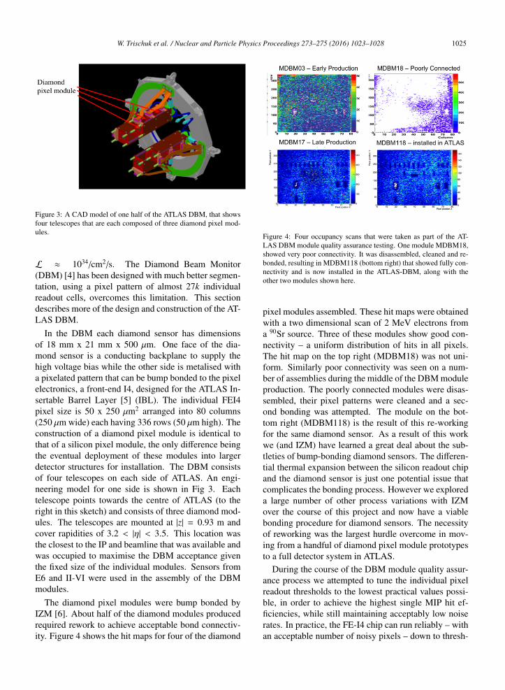
Figure 3: A CAD model of one half of the ATLAS DBM, that showsfour telescopes that are each composed of three diamond pixel mod-ules.
L ≈ 1034/cm2/s. The Diamond Beam Monitor(DBM) [4] has been designed with much better segmen-tation, using a pixel pattern of almost 27k individualreadout cells, overcomes this limitation. This sectiondescribes more of the design and construction of the AT-LAS DBM.
In the DBM each diamond sensor has dimensionsof 18 mm x 21 mm x 500 μm. One face of the dia-mond sensor is a conducting backplane to supply thehigh voltage bias while the other side is metalised witha pixelated pattern that can be bump bonded to the pixelelectronics, a front-end I4, designed for the ATLAS In-sertable Barrel Layer [5] (IBL). The individual FEI4pixel size is 50 x 250 μm2 arranged into 80 columns(250 μm wide) each having 336 rows (50 μm high). Theconstruction of a diamond pixel module is identical tothat of a silicon pixel module, the only difference beingthe eventual deployment of these modules into largerdetector structures for installation. The DBM consistsof four telescopes on each side of ATLAS. An engi-neering model for one side is shown in Fig 3. Eachtelescope points towards the centre of ATLAS (to theright in this sketch) and consists of three diamond mod-ules. The telescopes are mounted at |z| = 0.93 m andcover rapidities of 3.2 < |η| < 3.5. This location wasthe closest to the IP and beamline that was available andwas occupied to maximise the DBM acceptance giventhe fixed size of the individual modules. Sensors fromE6 and II-VI were used in the assembly of the DBMmodules.
The diamond pixel modules were bump bonded byIZM [6]. About half of the diamond modules producedrequired rework to achieve acceptable bond connectiv-ity. Figure 4 shows the hit maps for four of the diamond
Figure 4: Four occupancy scans that were taken as part of the AT-LAS DBM module quality assurance testing. One module MDBM18,showed very poor connectivity. It was disassembled, cleaned and re-bonded, resulting in MDBM118 (bottom right) that showed fully con-nectivity and is now installed in the ATLAS-DBM, along with theother two modules shown here.
pixel modules assembled. These hit maps were obtainedwith a two dimensional scan of 2 MeV electrons froma 90Sr source. Three of these modules show good con-nectivity – a uniform distribution of hits in all pixels.The hit map on the top right (MDBM18) was not uni-form. Similarly poor connectivity was seen on a num-ber of assemblies during the middle of the DBM moduleproduction. The poorly connected modules were disas-sembled, their pixel patterns were cleaned and a sec-ond bonding was attempted. The module on the bot-tom right (MDBM118) is the result of this re-workingfor the same diamond sensor. As a result of this workwe (and IZM) have learned a great deal about the sub-tleties of bump-bonding diamond sensors. The differen-tial thermal expansion between the silicon readout chipand the diamond sensor is just one potential issue thatcomplicates the bonding process. However we exploreda large number of other process variations with IZMover the course of this project and now have a viablebonding procedure for diamond sensors. The necessityof reworking was the largest hurdle overcome in mov-ing from a handful of diamond pixel module prototypesto a full detector system in ATLAS.
During the course of the DBM module quality assur-ance process we attempted to tune the individual pixelreadout thresholds to the lowest practical values possi-ble, in order to achieve the highest single MIP hit ef-ficiencies, while still maintaining acceptably low noiserates. In practice, the FE-I4 chip can run reliably – withan acceptable number of noisy pixels – down to thresh-
W. Trischuk et al. / Nuclear and Particle Physics Proceedings 273–275 (2016) 1023–1028 1025

Figure 5: A photo of the ATLAS Diamond Beam Monitor telescopesinstalled on the pixel support frame, prior to re-installation of thewhole package in ATLAS in the late fall of 2013.
olds of about 1000 electrons. However, in the courseof studying this in our diamond modules a number ofnon-linearities and spatial variations (across the rela-tively large FE-I4 chip) in the thresholds were identi-fied and we are developing tuning algorithms to achievethe lowest possible, uniform, threshold distribution forDBM module operation. While this is critical to the op-eration of diamond pixel modules – due to their lowerinitial MIP signal – it will be equally important for theultimate operation of the IBL silicon modules, after theyhave received doses approaching 1015/cm2 towards theend of their lifetime. The DBM is a trail-blazer for theoperation of irradiated silicon pixel detector systems.
Figure 5 shows two telescopes on one side of theDBM installed on the ATLAS pixel support frame. Thefull pixel detector, including the DBM has now been re-turned to the ATLAS experimental hall and reconnectedto its services. All eight DBM telescopes are fully func-tional and now being commissioned/tuned awaiting firstbeam in 2015.
4. 3D Diamond Sensors
Recently the RD42 collaboration has begun to ex-plore the possibility of producing 3-dimensional biasingelectrode structures through the diamond sensor mate-rial. Inspired by similar work in silicon [7] these elec-trodes, with separations as small as 25-50 μm, can pro-duce much larger, lateral, electric fields in the diamond,with much lower applied voltages. Figure 6 shows a
photograph of the first functional 3D diamond proto-type. In this device several areas were instrumented,some with just readout strips and others (near the top ofthe photo) with active 3D bias electrodes. The 3D biascolumns are produced with a high power laser, that pro-duces conducting graphitic carbon pillars through thediamond after relatively short (10s of seconds) expo-sures at each location. These conductive pillars are thenbiased (alternately to HV and ground) by a series ofinter-digitated bias networks on the back fo the diamondsensor.
Figure 6: A photo of the first 3D diamond sensor produced and testedin a beam by RD42. The top left corner of this device includes 3Dbiasing electrodes and crossed readout strips that allow MIP pulse-heights to be measured with a standard VLSI charged sensitive ampli-fiers in a testbeam. Below (and to the left) of that region are traditional2D readout strips (and a corresponding, biased backplane). This al-lows an in-situ comparison of the signal collected for these two biasconfigurations. Other areas of the diamond (to the bottom right) wereused to test the bias column generation parameters in the diamondmaterial but were not readout in the testbeam.
The MIP signal properties of this device were testedat CERN in late 2012. High energy protons weretracked with a silicon reference telescope and the re-sulting pulse-heights in the 3D diamond prototype wererecorded on strips that spanned 12 bias electrodes. Fig-ure 7 shows the average pulse height recorded for a biasof 25 V as a function of lateral position across the sen-sor. The lateral position in this figure is determined fromthe external, reference, telescope and not the 3D dia-mond device. One sees a number of ares of lower pulse-height (the blue regions) where we have independent ev-idence that one (or more) of the biasing electrodes werenot connected to the biasing network. However a rel-atively large, contiguous area of this prototype showsgood response and quite uniform charge collection (thegreen/yellow areas).
We have studied the pulse height distribution for the6x6 cell area in the middle right of the sensor, where
W. Trischuk et al. / Nuclear and Particle Physics Proceedings 273–275 (2016) 1023–10281026

Figure 7: The average pulse height recorded in the 3D diamond pro-totype as function of lateral position across the sensor face. Whilea number of areas show lower than average pulse-height, large areasshow uniform charge collection.
we had previously determined that no bias electrodeswere disconnected from their, respective, biasing grids.Figure 8 shows the 3D pulse-height distribution (inblue) overlaid with the pulse height distribution fromthe neighbouring conventional strip tracker. One seesvery good agreement between the two pulse-height dis-tributions. The remarkable achievement here is that theconventional tracker requires a 500 V bias (across the500 μm thick sensor) while the 3D device is only biasedwith 25 V. Encouraged by these initial results additionalwork is now underway to make more reliable and largerarea 3D electrode structures in diamond and to explorethe intrinsic position resolution of such 3D sensors.
5. Summary
Diamond sensors are finding widespread applicationsin high energy physics. Their radiation tolerance, fastsignal formation time and dimensional stability havemade them and ideal for use as beam monitors and lumi-nosity detectors during Run I at the LHC. They are nowbeing prepared for a variety of position sensitive detec-tor applications very near the interaction region of theLHC experiments where high particle fluxes and radia-tion fluences discourage the use of other technologies.The ATLAS experiment has installed a set of pixel tele-scopes that use diamond sensors and is preparing to use
Figure 8: A direct comparison of pulse heights from two regions of the3D prototype. The blue curve shows the result from the 3D electroderegion, biased at 25 V. The black curve shows the pulse heights fromthe traditional 2D diamond strip tracker, biased at 500 V.
these augment their luminosity and background mon-itoring capabilities in run II. CMS and LHCb are ex-ploring diamond sensors as options for their future pixeldetector upgrades. The RD42 collaboration has also be-gun to explore the possibility of biasing diamond sen-sors with 3D electrode structures, potentially providinga significant reduction in the sensor bias voltages neces-sary to achieve full charge collection in these devices.
References
[1] M. Artuso et al. (The RD42 Collaboration), ”RD42 Status Re-port: Development of Diamond Tracking Detectors for HighLuminosity Experiments at the LHC”, CERN/LHCC 2008-005.See also: http://indico.cern.ch/event/319702/ for the most recentupdate.
[2] Element Six Technologies, Global Innovation Centre, FermiAve., Harwell, OX11 0QR, United Kingdom.
[3] II-VI Incorporated, 375 Saxonburg Blvd., Saxonburg, PA,16056-9499, USA.
[4] H.Kagan, M.Mikuz, W.Trischuk, ”The ATLAS DiamondBeam Monitor TDR”, ATLAS Document ATU-DBM-001,09/14/2011.
[5] J.Albert et al. (The ATLAS-IBL Collaboration), ”Prototype AT-LAS IBL Modules using the FE-I4A Front-End Readout Chip”,arXiv:1209.1906 [physics.ins-det].
[6] Fraunhofer Institute Zuverlassigkeit Mikrointegration, Gustave-Meyer-Alle 25, D-13355, Berlin, Germany.
[7] S. Parker, C. Kenney and J. Segal ”3D, a new architecturefor solid state radiation detectors”, Nucl. Instrum. Meth. A395(1997).
W. Trischuk et al. / Nuclear and Particle Physics Proceedings 273–275 (2016) 1023–1028 1027

Appendix A. The RD42 Collaboration
M. Artuso27, F. Bachmair32, L. Bani32, M. Bartosik5, V. Bellini4, V. Belyaev21, B. Bentele2, E. Berdermann13,P. Bergonzo19, A. Bes12, J-M. Brom14, M. Bruzzi8, M. Cerv5, C. Chau31, G. Chiodini18, D. Chren6, V. Cindro17,G. Claus14, J. Collot12, S. Costa4, J. Cumalat2, A. Dabrowski5, R. D’Alessandro9, W. de Boer16, B. Dehning5,D. Dobos5, W. Dulinski14, V. Eremin26, R. Eusebi29, G. Forcolin20, J. Forneris30, H. Frais-Kolbl7, K.K. Gan23,M. Gastal5, M. Goffe14, J. Goldstein3, A. Golubev15, L. Gonella1, A. Gorisek17, L. Graber11, E. Grigoriev15,J. Grosse-Knetter11, M. Guthoff5, I. Haughton20, D. Hidas25, D. Hits32, M. Hoeferkamp22, T. Hofmann5, J. Hosslet14,J-Y. Hostachy12, F. Hugging1, H. Jansen5, J. Janssen1, H. Kagan23,♦, K. Kanxheri24, G. Kasieczka32, R. Kass23,F. Kassel16, M. Kis13, G. Kramberger17, S. Kuleshov15, A. Lacoste12, S. Lagomarsino9, A. Lo Giudice30,C. Maazouzi14, I. Mandic17, C. Manfredotti30, C. Mathieu14, N. McFadden22, G. McGoldrick31, M. Menichelli24,M. Mikuz17, A. Morozzi24, J. Moss23, R. Mountain27, S. Murphy20, A. Oh20, P. Olivero30, G. Parrini9, D. Passeri24,M. Pauluzzi24, H. Pernegger5, R. Perrino18, F. Picollo30, M. Pomorski19, R. Potenza4, A. Quadt11, A. Re30, G. Riley28,S. Roe5, M. Sapinski5, M. Scaringella8, S. Schnetzer25, T. Schreiner7, S. Sciortino9, A. Scorzoni24, S. Seidel22,L. Servoli24, A. Sfyrla5, G. Shimchuk15, S. Smith23, B. Sopko6, V. Sopko6, S. Spagnolo18, S. Spanier28, K. Stenson2,R. Stone25, C. Sutera4, A. Taylor22, M. Traeger13, D. Tromson19, W. Trischuk31,♦, C. Tuve4, L. Uplegger10,J. Velthuis3, N. Venturi31, E. Vittone30, S. Wagner2, R. Wallny32, J.C. Wang27, P. Weilhammer5, J. Weingarten11,C. Weiss5, T. Wengler5, N. Wermes1, M. Yamouni12, M. Zavrtanik17
1 Universitat Bonn, Bonn, Germany, 2 University of Colorado, Boulder, CO, USA, 3 University of Bristol, Bristol,UK, 4 INFN/University of Catania, Catania, Italy, 5 CERN, Geneva, Switzerland, 6 Czech Technical Univ., Prague,Czech Republic, 7 FWT, Wiener Neustadt, Austria, 8 INFN/University of Florence, Florence, Italy, 9 Departmentof Energetics/INFN, Florence, Italy, 10 FNAL, Batavia, USA, 11 Universitat Goettingen, Goettingen, Germany,12 LPSC-Grenoble, Grenoble, France, 13 GSI, Darmstadt, Germany, 14 IPHC, Strasbourg, France, 15 ITEP, Moscow,Russia, 16 Universitat Karlsruhe, Karlsruhe, Germany, 17 Jozef Stefan Institute, Ljubljana, Slovenia, 18 INFN-Lecce,Lecce, Italy, 19 CEA-LIST Technologies Avancees, Saclay, France, 20 University of Manchester, Manchester, UK,21 MEPHI Institute, Moscow, Russia, 22 University of New Mexico, Albuquerque, NM, USA, 23 The Ohio StateUniversity, Columbus, OH, USA, 24 INFN-Perugia, Perugia, Italy, 25 Rutgers University, Piscataway, NJ, USA,26 Ioffe Institute, St. Petersburg, Russia, 27 Syracuse University, Syracuse, NY, USA, 28 University of Tennessee,Knoxville, TN, USA, 29 Texas A&M, College Park Station, TX, USA, 30 University of Torino, Torino, Italy,31 University of Toronto, Toronto, ON, Canada, 32 ETH Zurich, Zurich, Switzerland
♦ Spokespersons
W. Trischuk et al. / Nuclear and Particle Physics Proceedings 273–275 (2016) 1023–10281028