Diamond Detectors John Smedley "Single crystal diamond photodiode for soft X-ray radiometry" Jeffrey...
31
Diamond Detectors John Smedley "Single crystal diamond photodiode for soft X-ray radiometry" Jeffrey W. Keister and John Smedley Nuclear Instruments and Methods in Physics Research Section A: Accelerators, Spectrometers, Detectors and Associated Equipment, Volume 606, Issue 3, 21 July 2009, Pages 774-779
-
date post
19-Dec-2015 -
Category
Documents
-
view
220 -
download
0
Transcript of Diamond Detectors John Smedley "Single crystal diamond photodiode for soft X-ray radiometry" Jeffrey...
Diamond Detectors
John Smedley
"Single crystal diamond photodiode for soft X-ray radiometry"Jeffrey W. Keister and John Smedley
Nuclear Instruments and Methods in Physics Research Section A: Accelerators, Spectrometers, Detectors and Associated Equipment,
Volume 606, Issue 3, 21 July 2009, Pages 774-779
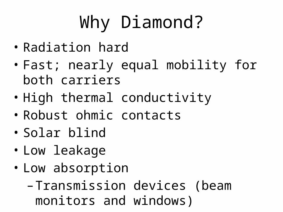
Why Diamond?• Radiation hard• Fast; nearly equal mobility for both carriers• High thermal conductivity• Robust ohmic contacts• Solar blind• Low leakage• Low absorption
– Transmission devices (beam monitors and windows)

X-rays
Diamond as a Detector
Diamond Metalized both sides
X-rays
Two detector geometries• X-rays excite energetic electrons which
scatter to produce carriers • Soft x-rays generate carriers near
incident surface, allowing electron and hole motion to be separated by biasing
• Harder x-rays go all the way through, creating a column of charge
• Initial oxygen termination achieved by acid etch or ozone exposure
• Diamond metalized on both surfaces with 3mm diameter electrodes
• Leakage is <1 pA for oxygen terminated diamonds, even for 1kV bias

Metal-Diamond Interface• We will consider two types of contacts:
– Contacts which allow charge carriers to pass with sufficient ease to require the diamond to remain charge neutral on average. These contacts allow photoconductive gain, and we’ll call them injecting.
– Contacts which restrict the flow of charge to an extent sufficient to allow the diamond to charge. We’ll call these contacts blocking.
• For diamond with oxygen surface termination, all metal contacts tested (Ti/Pt, Pt, Al, Cu, Nb, & Mo) have been blocking
• Oxygen can be removed by thermal annealing, causing contacts to become injecting (remember this – it will come up later)
• For Moly, thermal annealing has been used to create injecting Mo2C contacts
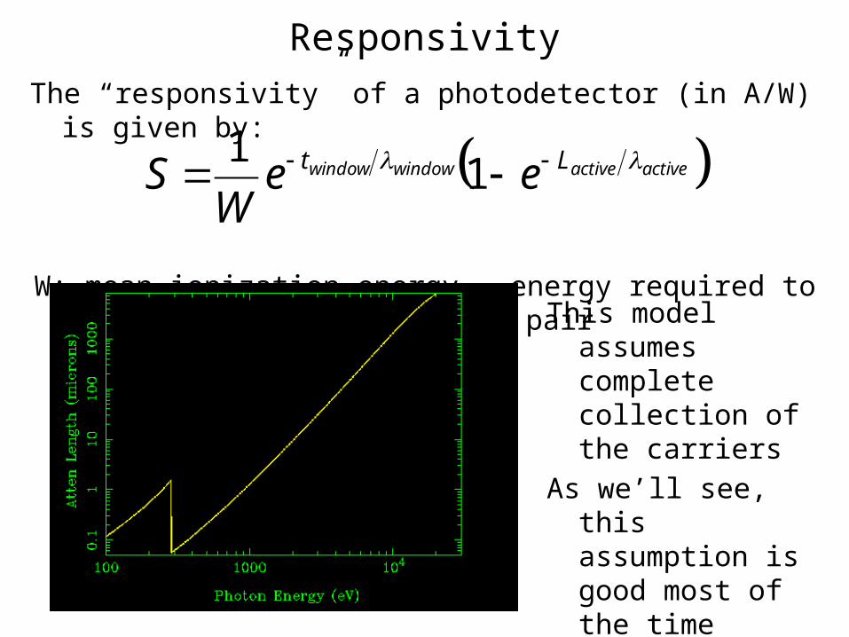
The “responsivity” of a photodetector (in A/W) is given by:
W: mean ionization energy – energy required to create an e-h pair
Responsivity
activeactivewindowwindow Lt eeW
S 11
This model assumes complete collection of the carriers
As we’ll see, this assumption is good most of the time (except near the C edge)
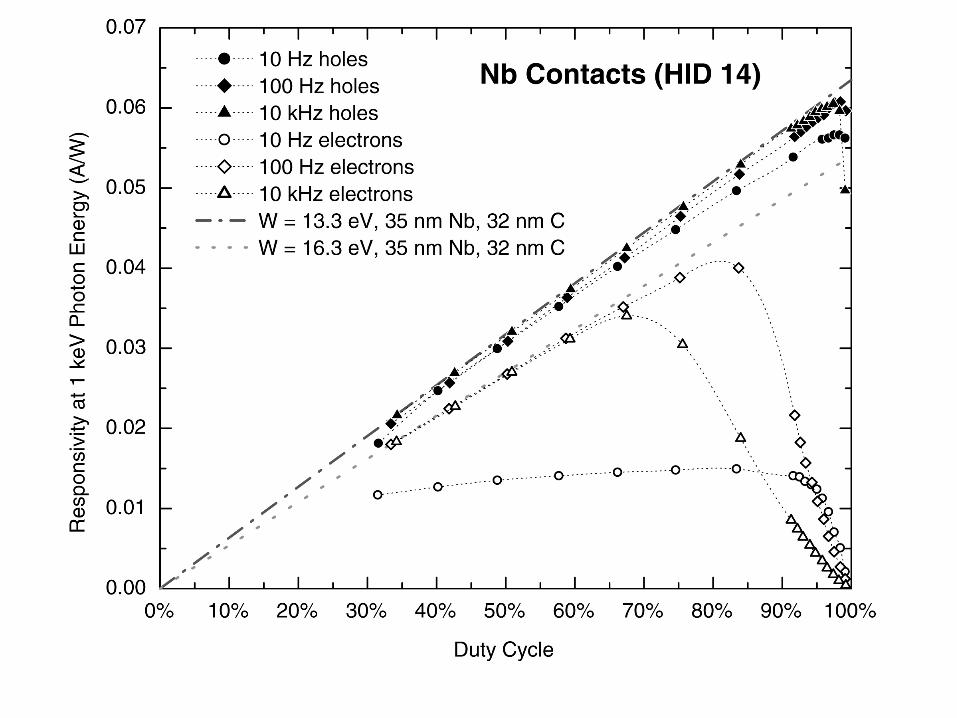
Trapping and Pulsed Bias
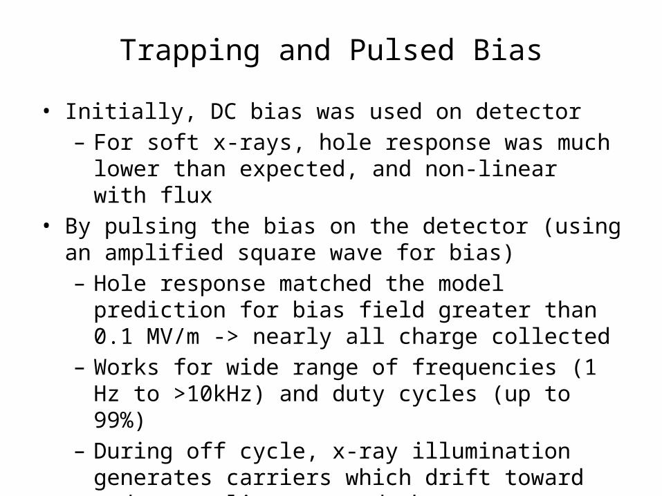
• Initially, DC bias was used on detector– For soft x-rays, hole response was much lower than
expected, and non-linear with flux• By pulsing the bias on the detector (using an amplified square
wave for bias)– Hole response matched the model prediction for bias field
greater than 0.1 MV/m -> nearly all charge collected– Works for wide range of frequencies (1 Hz to >10kHz) and
duty cycles (up to 99%)– During off cycle, x-ray illumination generates carriers which
drift toward and neutralize trapped charge

)1)()(1
(][ ][][][][ C
active
C
C
Ti
Ti
Pt
Pt tttt
C
eeeeW
S
J. Keister & J. Smedley, NIM A, 606 774 (2009)

0.0001
0.001
0.01
0.1
0 20 40 60 80 100 120 140 160
Res
po
nsiv
ity (A
/W)
Voltage
Hole Response (1 keV)
Hole collection saturated for 0.3 mm thickness
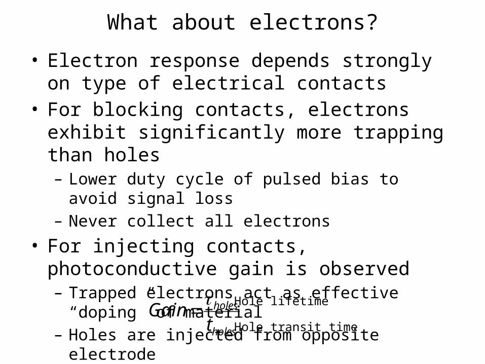
What about electrons?
• Electron response depends strongly on type of electrical contacts
• For blocking contacts, electrons exhibit significantly more trapping than holes – Lower duty cycle of pulsed bias to avoid signal loss– Never collect all electrons
• For injecting contacts, photoconductive gain is observed– Trapped electrons act as effective “doping” of material– Holes are injected from opposite electrode
holes
holes
tGain
Hole lifetime
Hole transit time
0.00001
0.0001
0.001
0.01
0.1
1
10
0 20 40 60 80 100 120 140 160 180
Res
po
nsiv
ity (A
/W)
Voltage
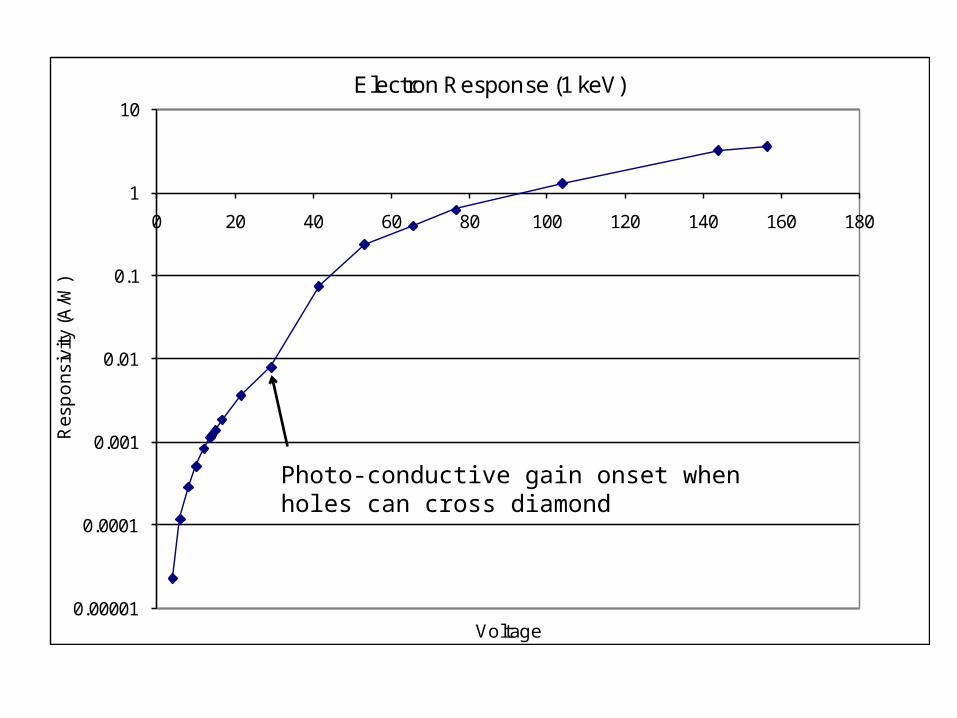
Electron Response (1 keV)
Photo-conductive gain onset when holes can cross diamond
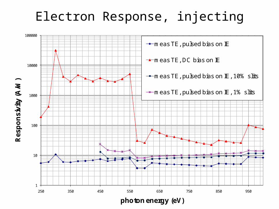
1
10
100
1000
10000
100000
250 350 450 550 650 750 850 950
Res
po
nsi
vity
(A
/W)
photon energy (eV)
meas TE, pulsed bias on IE
meas TE, DC bias on IE
meas TE, pulsed bias on IE, 10% slits
meas TE, pulsed bias on IE, 1% slits
Electron Response, injecting
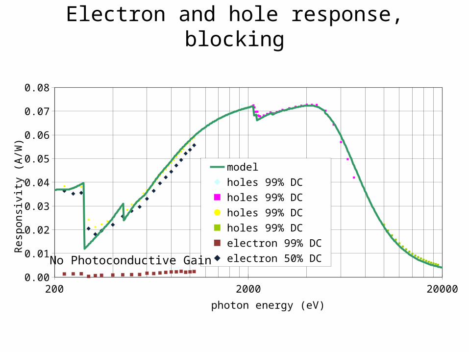
200 2000 200000.00
0.01
0.02
0.03
0.04
0.05
0.06
0.07
0.08
model
holes 99% DC
holes 99% DC
holes 99% DC
holes 99% DC
electron 99% DC
electron 50% DC
photon energy (eV)
Re
spo
nsi
vity
(A
/W)
Electron and hole response, blocking
No Photoconductive Gain

Responsivity Conclusions• Holes have larger CCD than electrons in these
synthetic diamonds (due to ultra low N content) • Charge collection for holes is limited only by diffusion
of carriers if field is low – for E>0.1 MV/m, all holes collected
• Simple model of Responsivity yields a pair creation energy of 13.3 +/- .5 eV
• Electron trapping occurs in bulk diamond; cannot collect all electrons – leads to PC gain w/ injecting contacts
• Can sweep trapped charge by irradiating diamond w/o bias

White Beam Test• Diamond detector used on beam at X28C, with 17W of X-
ray power, ranging from 6 keV to 15 keV• Intercepted ~3% of beam• Ion chamber used for low power calibration, copper
calorimeter for higher power• Generated 40 mA of current in a 2mm2 area• 2 A/cm2
• Can see NSLS ringrepetition frequencyon detector
0 2000 4000 6000 8000 10000 12000 14000 16000 18000 200000.00E+00
5.00E+11
1.00E+12
1.50E+12
2.00E+12
2.50E+12
3.00E+12
3.50E+12
4.00E+12
4.50E+12
5.00E+12
Energy (eV)
Flux
(pho
tons
/sec
/0.1
%BW
)
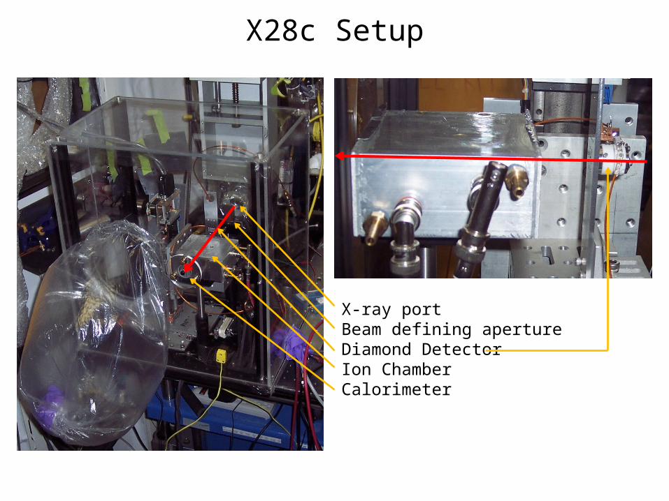
X28c Setup
X-ray portBeam defining apertureDiamond DetectorIon ChamberCalorimeter
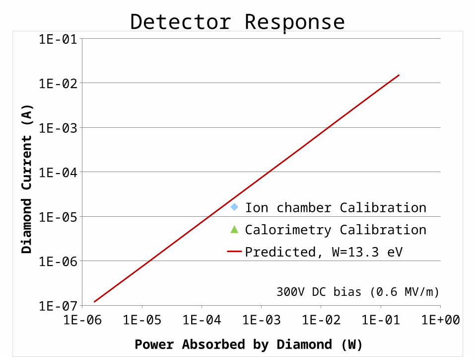
Detector Response
1E-06 1E-05 1E-04 1E-03 1E-02 1E-01 1E+001E-07
1E-06
1E-05
1E-04
1E-03
1E-02
1E-01
Ion chamber Calibration
Calorimetry Calibration
Predicted, W=13.3 eV
Power Absorbed by Diamond (W)
Dia
mon
d Cu
rren
t (A)
300V DC bias (0.6 MV/m)

Pulse response, 2 MV/m

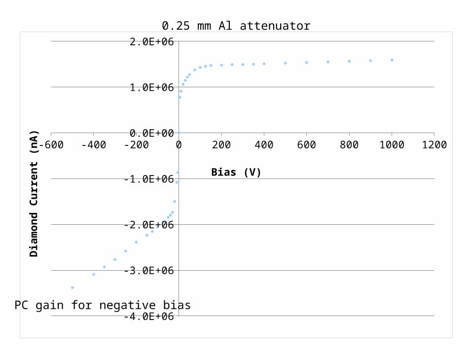
Radiation Hard?• The diamond was not obviously harmed by absorption of 108
rads of x-rays• However, continuously driving 16+ mA of current at up to 1 kV
bias (16 W of electrical power) caused significant heating of device
• This lead to a change in the nature of the response– Initially, diamond was a diode, with blocking contacts– During high flux measurement, photoconduction was observed for
negative bias– This change in the contact was permanent – loss of oxygen?
• Subsequent response maps showed that photoconductive region is tiny (~200 microns across), and that a region of PC gain for opposite polarity is present in the unirradiated area

-1000 -800 -600 -400 -200 0 200 400 600 800 1000
-250
-200
-150
-100
-50
0
50
100
150
200
Bias (V)
Diam
ond
Curr
ent (
nA)
4.5 mm Al attenuator
-600 -400 -200 0 200 400 600 800 1000 1200
-4.0E+06
-3.0E+06
-2.0E+06
-1.0E+06
0.0E+00
1.0E+06
2.0E+06
Bias (V)
Diam
ond
Curr
ent (
nA)
PC gain for negative bias
0.25 mm Al attenuator
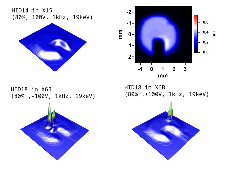
HID14 in X15(80%, 100V, 1kHz, 19keV)
HID18 in X6B (80% ,-100V, 1kHz, 19keV)
HID18 in X6B (80% ,+100V, 1kHz, 19keV)
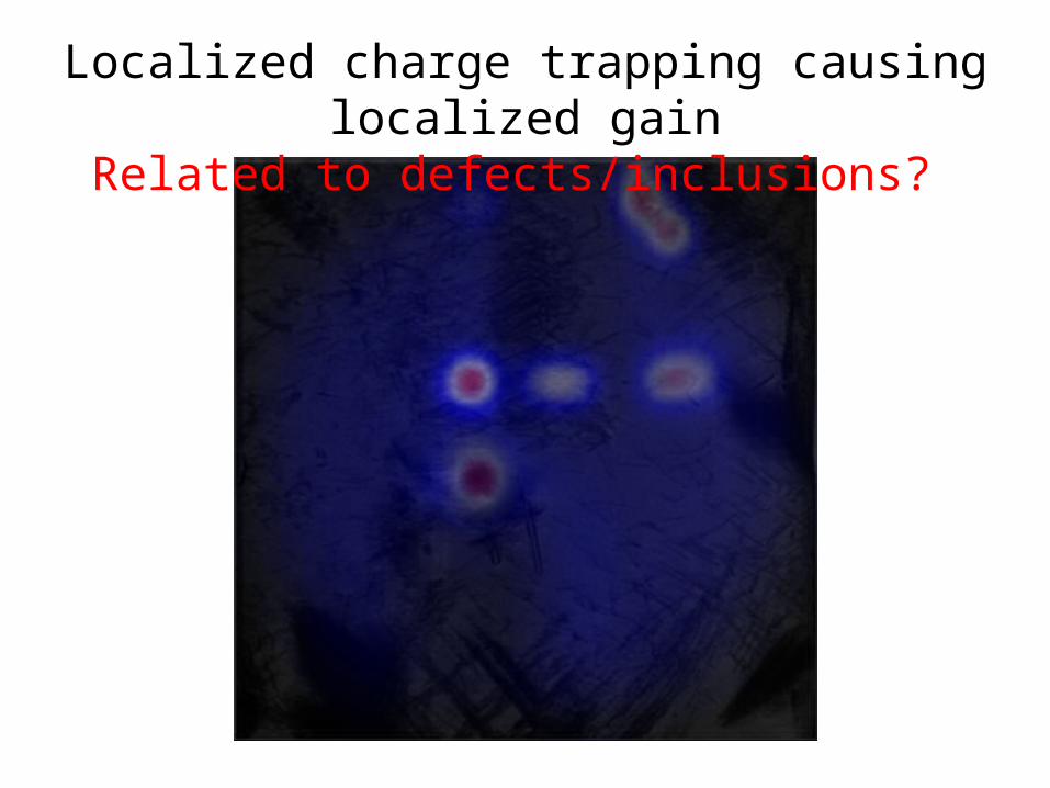
Localized charge trapping causing localized gainRelated to defects/inclusions?

Conclusions & Thoughts• Diamond detector response is linear from 100pW – 1W
incident x-ray power, and predictable for photon energies from 0.2-28 keV
• For soft x-rays, pulsed bias allows clearing of trapped charge to achieve (nearly) full charge collection
• Above 4keV, DC bias is adequate, even at high flux– Pulsed bias is still useful to prevent PC gain, and limit current
• Temporal response of detector is consistent with carrier velocity and thickness
• Up to 40 mA (2 A/cm2) passed through diamond• Due to it’s mechanical and thermal properties,
diamond is already a candidate to replace beryllium for x-ray windows for some NSLS II beamlines – can we instrument these windows?

Thank you for your attention!
• Thanks to Jen Bohon, Wei Chen, Elaine DiMasi, Jim Distel, Bin Dong, Dan Fischer, Joe Harder, Abdel Isakovic, Cherno Jaye, Jeff Keister, Zhenxian Liu, Erik Muller, Veljko Radeka, Balaji Raghothamachar, Triveni Rao, Pavel Rehak, Bill Smith, Jean Jordan-Sweet, John Walsh
• C-AD Diamond Team: Ilan Ben-Zvi, Andrew Burrill, Xiangyun Chang, David Pate, Erdong Wang, Qiong Wu
• Simulations: Richard Busby, Dimitre Dimitrov• Beamlines: U2A, U2B, U3C, U7A, X3B, X6B, X8A, X16C, X19C,
X20A&C, X28C

Photons produce initial carriersElectrons drift through diamond
Some electrons are trapped in materialAct as effective p-type doping as long they are trapped
On average, one hole is injected into diamond for each trapped electron, keeping material charge neutral
Holes drift through diamondNew holes enter, each time adding current
Process continues until the hole is trapped in the material or the trapped electron is neutralized
Photoconductive Gain
hn
holes
holes
tGain
Hole lifetime
Hole transit time

Ene
rgy
Filled States
Empty States
Some photons lost to absorption in metal layer (atomic absorption edges)Photons produce energetic electrons via photoelectric absorption
Penetration depth strong function of photon energyElectrons scatter, produce electron-hole pairs
Some e- lost to recombination at metal interface, possibly surface trapping
Bias determines which carrier crosses diamond for soft x-raysFor harder x-rays (>3 keV), both carriers participate
Carriers lose energy via e--e- and e--phonon scatteringEventually, e- reaches the conduction band min, hole reached valance band max
Some carriers are trappedMost drift through
Current induced on far electrode as soon as carriers begin movingTrapped carriers modify field in diamond
Bulk Trap
Eg
Other surface metallizedSome e- trapped at surface
Most will be collected
Surface Trap
Electron Transport in DiamondPhoton Generated, Detector Case
Surface Trap
hn
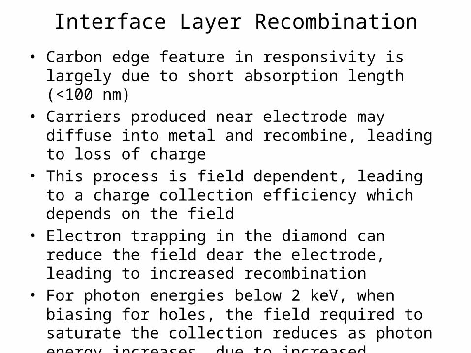
Interface Layer Recombination
• Carbon edge feature in responsivity is largely due to short absorption length (<100 nm)
• Carriers produced near electrode may diffuse into metal and recombine, leading to loss of charge
• This process is field dependent, leading to a charge collection efficiency which depends on the field
• Electron trapping in the diamond can reduce the field dear the electrode, leading to increased recombination
• For photon energies below 2 keV, when biasing for holes, the field required to saturate the collection reduces as photon energy increases, due to increased penetration depth
• For photon energies above 4keV, the photons are being absorbed in the bulk of the diamond, making it impossible to differentiate electron motion from hole motion

0 0.1 0.2 0.3 0.4 0.5 0.6 0.7 0.8-0.01
0.00
0.01
0.02
0.03
0.04
0.05
0.06
0.07
0.08
500 um diamond, Contact: 20 nm Mo, W =13.3 eV
350 eV (0.1 um) 600 eV (0.3 um)
1000 eV (1.3 um) 2100 eV (10.9 um)
Applied Field (MV/m)
Resp
onsi
vity
(A/W
)
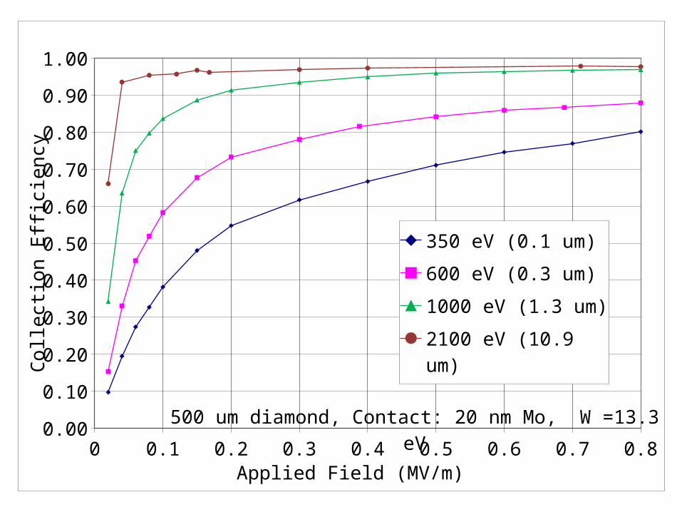
0 0.1 0.2 0.3 0.4 0.5 0.6 0.7 0.80.00
0.10
0.20
0.30
0.40
0.50
0.60
0.70
0.80
0.90
1.00
500 um diamond, Contact: 20 nm Mo, W =13.3 eV
350 eV (0.1 um)
600 eV (0.3 um)
1000 eV (1.3 um)
2100 eV (10.9 um)
Applied Field (MV/m)
Colle
ction
Effi
cien
cy

0 0.1 0.2 0.3 0.4 0.5 0.6 0.7 0.8-0.01
0.00
0.01
0.02
0.03
0.04
0.05
0.06
0.07
0.08
350 eV (0.1 um) 600 eV (0.3 um)1000 eV (1.3 um) 2100 eV (10.9 um)4000 eV (75 um) 19 keV (7.1 mm)
Applied Field (MV/m)
Resp
onsi
vity
(A/W
)