
Evaluating the AD5420 Single-Channel, 16-Bit, Serial Input ...
Upload
trinhxuyenCategory
view
223download
0
Stereo, 24-Bit, 192kHz8x Oversampling Digital Interpolation Filter
49%FPO
DF1706
DESCRIPTIONThe DF1706 is a high performance, stereo, 8Xoversampling digital interpolation filter designed forhigh-end consumer and professional audio applica-tions. The DF1706 supports 24-bit, 192kHz operationand features user-programmable functions, including
FEATURES COMPANION DIGITAL FILTER FOR THE
PCM1704 24-BIT AUDIO DAC
HIGH PERFORMANCE FILTER:Stopband Attenuation: –115dBPassband Ripple: ±0.00005dB
AUDIO INTERFACE:Input Data Formats: Standard, Left-Justified, and I2SInput Word Length: 16, 20, or 24 BitsOutput Word Length: 16, 18, 20, or 24 BitsSampling Frequency: 32kHz to 192kHz
SerialInputI/F
ModeControl
I/F
8X OversamplingDigital Filter with
FunctionController
Crystal/OSC
XTI
SCK
XTO CLKO(SF0) (SF1) (SRO) VDD DGND
Output I/F
BCKO
(I2 S
)
(IW
1)
(IW
0)
(OW
1)
(OW
0)
WCKO
DOL
DOR
MC/LRIP
MD/CKO
LRCIN
DIN
BCKIN
x4
MODEML/RESV
(MUTE)
RST(DEM) Power Supply
Copyright © 2001, Texas Instruments Incorporated SBAS182 Printed in U.S.A. January, 2001
www.ti.com
DF1706
SYSTEM CLOCK: 128fS, 192fS, 256fS,384fS, 512fS, 768fS
ON-CHIP CRYSTAL OSCILLATOR
PROGRAMMABLE FUNCTIONS:Hardware or Software Control ModesSharp or Slow Roll-Off Filter ResponseSoft MuteDigital De-EmphasisIndependent Left/Right Digital Attenuation
+3.3V SINGLE-SUPPLY OPERATION
SMALL SSOP-28 PACKAGE
selectable filter response, de-emphasis, attenuation,and input/output data formats.
The DF1706 is the ideal companion for TexasInstruments’s PCM1704 24-bit audio Digital-to-Ana-log (D/A) converter. This combination allows for theconstruction of very high-performance audio systemsand components.

DF17062SBAS182
SPECIFICATIONSAll specifications at TA = +25°C, VDD = 3.3V, fS = 44.1kHz, system clock = 256fS/384fS, 16-bit data, unless otherwise noted.
DF1706E
PARAMETER CONDITIONS MIN TYP MAX UNITS
RESOLUTION 24 Bits
INPUT DATA FORMATAudio Data Interface Format Standard , Left-Justified , I2SAudio Data Bit Length 16, 20, 24 SelectableAudio Data Format MSB First, Binary Two’s ComplementSampling Frequency fS 32 192 kHzSystem Clock Frequency(1) 128/192/256/384/512/768 fS
OUTPUT DATA FORMATAudio Data Interface Format Right-JustifiedAudio Data Bit Length 16, 20, 24 SelectableAudio Data Format MSB First, Binary Two’s Complement
DIGITAL INPUT/OUTPUT CMOS CompatibleInput Logic Level: VIH 0.7VDD V
VIL 0.3VDD VOutput Logic Level: VOH IOH = 2mA 2.4 V
VOL IOL = 4mA 1.0 V
CLKO AC CHARACTERISTICS(2)
Rise Time tR 20% to 80% VDD, 20pF 4 nsFall Time tF 80% to 20% VDD, 20pF 3 nsDuty Cycle(2) 20pF Load 50 %
DIGITAL FILTER PERFORMANCEFilter Characteristics 1 (Sharp Roll-Off)
Passband ±0.00005dB 0.454 fS–3dB 0.493 fS
Stopband 0.546 fSPassband Ripple ±0.00005 dBStopband Attenuation Stopband = 0.546fS –115 dB
Filter Characteristics 2 (Slow Roll-Off)Passband Ripple ±0.0001dB 0.254 fS
–3dB 0.460 fSStopband 0.732 fSPassband Ripple ±0.0001 dBStopband Attenuation Stopband = 0.748fS –100 dB
Delay Time 45.125/fS secDe-Emphasis Error ±0.004 dB
POWER-SUPPLY REQUIREMENTSVoltage Range VDD 3.0 3.3 3.6 VDCSupply Current IDD VDD = 3.3V 30 45 mAPower Dissipation VDD = 3.3V 99 149 mW
TEMPERATURE RANGEOperation –25 +85 °CStorage –55 +125 °CThermal Resistance, θJA SSOP-28 100 °C
NOTES: (1) Refer to Table I. (2) Crystal resonator used.
DF1706 3SBAS182
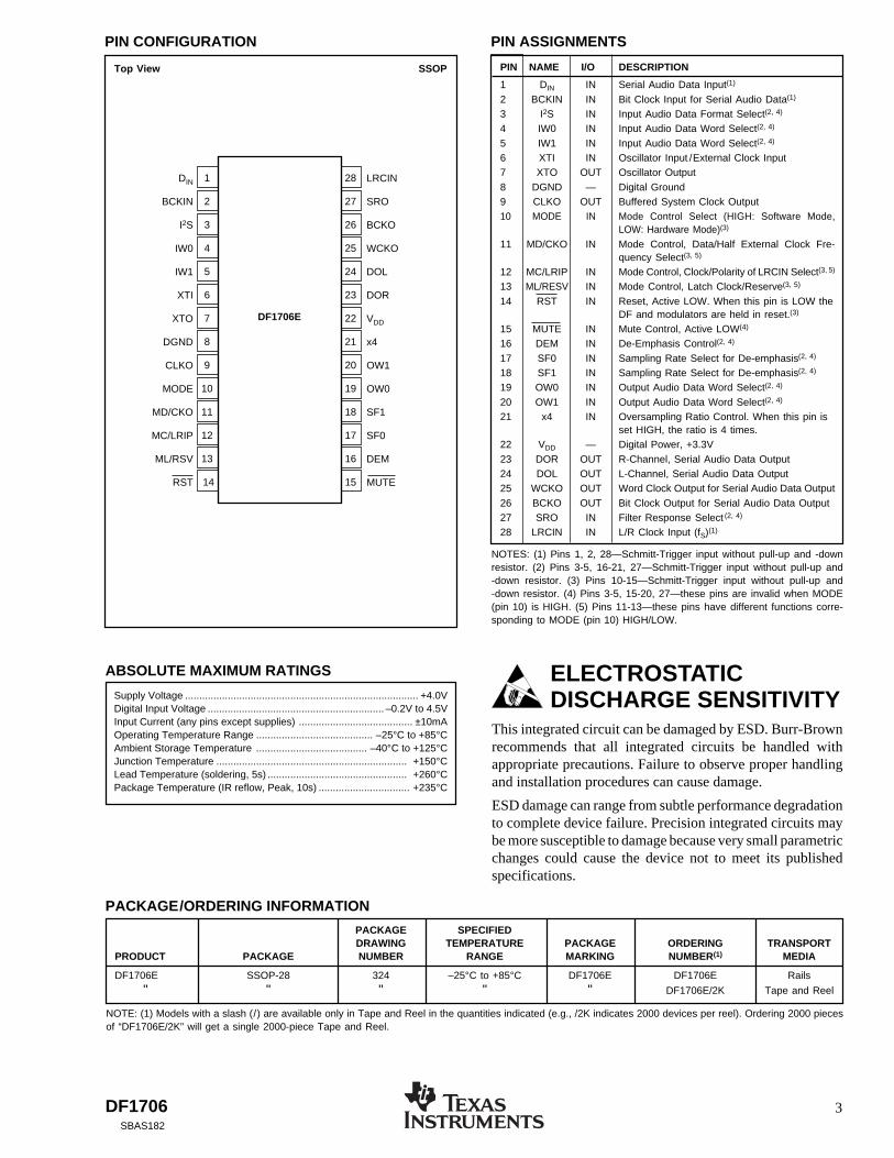
PIN NAME I/O DESCRIPTION
1 DIN IN Serial Audio Data Input(1)
2 BCKIN IN Bit Clock Input for Serial Audio Data(1)
3 I2S IN Input Audio Data Format Select(2, 4)
4 IW0 IN Input Audio Data Word Select(2, 4)
5 IW1 IN Input Audio Data Word Select(2, 4)
6 XTI IN Oscillator Input /External Clock Input7 XTO OUT Oscillator Output8 DGND — Digital Ground9 CLKO OUT Buffered System Clock Output10 MODE IN Mode Control Select (HIGH: Software Mode,
LOW: Hardware Mode)(3)
11 MD/CKO IN Mode Control, Data/Half External Clock Fre-quency Select(3, 5)
12 MC/LRIP IN Mode Control, Clock/Polarity of LRCIN Select(3, 5)
13 ML/RESV IN Mode Control, Latch Clock/Reserve(3, 5)
14 RST IN Reset, Active LOW. When this pin is LOW theDF and modulators are held in reset.(3)
15 MUTE IN Mute Control, Active LOW(4)
16 DEM IN De-Emphasis Control(2, 4)
17 SF0 IN Sampling Rate Select for De-emphasis(2, 4)
18 SF1 IN Sampling Rate Select for De-emphasis(2, 4)
19 OW0 IN Output Audio Data Word Select(2, 4)
20 OW1 IN Output Audio Data Word Select(2, 4)
21 x4 IN Oversampling Ratio Control. When this pin isset HIGH, the ratio is 4 times.
22 VDD — Digital Power, +3.3V23 DOR OUT R-Channel, Serial Audio Data Output24 DOL OUT L-Channel, Serial Audio Data Output25 WCKO OUT Word Clock Output for Serial Audio Data Output26 BCKO OUT Bit Clock Output for Serial Audio Data Output27 SRO IN Filter Response Select (2, 4)
28 LRCIN IN L/R Clock Input (fS)(1)
NOTES: (1) Pins 1, 2, 28—Schmitt-Trigger input without pull-up and -downresistor. (2) Pins 3-5, 16-21, 27—Schmitt-Trigger input without pull-up and-down resistor. (3) Pins 10-15—Schmitt-Trigger input without pull-up and-down resistor. (4) Pins 3-5, 15-20, 27—these pins are invalid when MODE(pin 10) is HIGH. (5) Pins 11-13—these pins have different functions corre-sponding to MODE (pin 10) HIGH/LOW.
PIN ASSIGNMENTSPIN CONFIGURATION
ELECTROSTATICDISCHARGE SENSITIVITY
This integrated circuit can be damaged by ESD. Burr-Brownrecommends that all integrated circuits be handled withappropriate precautions. Failure to observe proper handlingand installation procedures can cause damage.
ESD damage can range from subtle performance degradationto complete device failure. Precision integrated circuits maybe more susceptible to damage because very small parametricchanges could cause the device not to meet its publishedspecifications.
Supply Voltage .................................................................................. +4.0VDigital Input Voltage .............................................................. –0.2V to 4.5VInput Current (any pins except supplies) ........................................ ±10mAOperating Temperature Range ......................................... –25°C to +85°CAmbient Storage Temperature ....................................... –40°C to +125°CJunction Temperature ................................................................... +150°CLead Temperature (soldering, 5s) ................................................. +260°CPackage Temperature (IR reflow, Peak, 10s) ................................ +235°C
ABSOLUTE MAXIMUM RATINGS
DIN
BCKIN
I2S
IW0
IW1
XTI
XTO
DGND
CLKO
MODE
MD/CKO
MC/LRIP
ML/RSV
RST
LRCIN
SRO
BCKO
WCKO
DOL
DOR
VDD
x4
OW1
OW0
SF1
SF0
DEM
MUTE
1
2
3
4
5
6
7
8
9
10
11
12
13
14
28
27
26
25
24
23
22
21
20
19
18
17
16
15
DF1706E
PACKAGE SPECIFIEDDRAWING TEMPERATURE PACKAGE ORDERING TRANSPORT
PRODUCT PACKAGE NUMBER RANGE MARKING NUMBER(1) MEDIA
DF1706E SSOP-28 324 –25°C to +85°C DF1706E DF1706E Rails
" " " " " DF1706E/2K Tape and Reel
NOTE: (1) Models with a slash (/) are available only in Tape and Reel in the quantities indicated (e.g., /2K indicates 2000 devices per reel). Ordering 2000 piecesof “DF1706E/2K” will get a single 2000-piece Tape and Reel.
PACKAGE/ORDERING INFORMATION
Top View SSOP

DF17064SBAS182
TYPICAL PERFORMANCE CURVESAt TA = +25°C, VDD = ±3.3V, fS = 44.1kHz, System Clock = 256fS/384fS, 16-bit data, unless otherwise noted.
DIGITAL FILTER (DE-EMPHASIS OFF, fS = 44.1kHz)
DE-EMPHASIS AND DE-EMPHASIS ERROR
0 4321
Frequency (fS)
20
0
–20
–40
–60
–80
–100
–120
–140
–160
–180
–200
FREQUENCY RESPONSE (Sharp Roll-Off)
Atte
nuat
ion
(dB
)
0 0.500.450.400.30 0.350.250.200.150.100.05
Frequency (fS)
0.00010
0.00008
0.00006
0.00004
0.00002
0
–0.00002
–0.00004
–0.00006
–0.00008
–0.00010
PASSBAND RIPPLE (Sharp Roll-Off)
Atte
nuat
ion
(dB
)
0 4321
Frequency (fS)
0
–20
–40
–60
–80
–100
–120
–140
–160
–180
–200
FREQUENCY RESPONSE (Slow Roll Off)
Atte
nuat
ion
(dB
)
0 0.1 0.2 0.3 0.4 0.5 0.70.6
Frequency (fS)
TRANSITION CHARACTERISTIC (Slow Roll Off)0
–5
–10
–15
Atte
nuat
ion
(dB
)
0 1412108642
Frequency (kHz)
0
–2
–4
–6
–8
–10
DE-EMPHASIS (fS = 32kHz)
Leve
l (dB
)
0 14128 10642
Frequency (kHz)
0.010
0.008
0.006
0.004
0.002
0
–0.002
–0.004
–0.006
–0.008
–0.010
DE-EMPHASIS ERROR (fS = 32kHz)
Err
or (
dB)

DF1706 5SBAS182
TYPICAL PERFORMANCE CURVES (Cont.)At TA = +25°C, VDD = ±3.3V, fS = 44.1kHz, System Clock = 256fS/384fS, 16-bit data, unless otherwise noted.
0 20181610 14128642
Frequency (kHz)
0
–2
–4
–6
–8
–10
DE-EMPHASIS (fS = 44.1kHz)Le
vel (
dB)
0 20181610 14128642
Frequency (kHz)
DE-EMPHASIS ERROR (fS = 44.1kHz)0.010
0.008
0.006
0.004
0.002
0
–0.002
–0.004
–0.006
–0.008
–0.010
Err
or (
dB)
0 2220181610 14128642
Frequency (kHz)
0
–2
–4
–6
–8
–10
DE-EMPHASIS (fS = 48kHz)
Leve
l (dB
)
0 2220181610 14128642
Frequency (kHz)
DE-EMPHASIS ERROR (fS = 48kHz)0.010
0.008
0.006
0.004
0.002
0
–0.002
–0.004
–0.006
–0.008
–0.010
Err
or (
dB)

DF17066SBAS182
SYSTEM CLOCK REQUIREMENTS
The system clock of the DF1706 can be supplied by either anexternal clock signal at XTI (pin 6), or by the on-chip crystaloscillator. The system clock rate must run at 128fS, 192fS,256fS, 384fS, 512fS, or 768fS, where fS is the audio samplingrate. When a 128fS or 192fS system clock is applied toDF1706, the Over-Sampling Ratio (OSR) of the DF1706'sdigital filter should be four times instead of eight times. TheOSR can be selected by the x4 pin (pin 21) in hardware modeor x4 bit on MODE 2 register in software mode.
It should be noted that a 768fS system clock cannot be usedwhen fS is larger than 48kHz. Both 128fS and 192fS systemclock can be used when fS is larger than 96kHz. In addition,the on-chip crystal oscillator is limited to a maximum fre-quency of 24.0MHz. Table I shows the typical system clockfrequencies for selected sample rates.
The DF1706 includes a system clock detection circuit thatdetermines the system clock rate in use. The circuit comparesthe system clock input (XTI) frequency with the LRCIN inputrate to determine the system clock multiplier. Ideally, LRCINand BCKIN should be derived from the system clock toensure proper synchronization. If the phase difference be-tween the system clock and LRCIN is larger than ±4 bit clock(BCKIN) periods, the synchronization of the system andLRCIN clocks will be performed automatically by the DF1706.
Timing requirements for the system clock input are shown inFigure 1.
SYSTEM CLOCK FREQUENCY (MHz)
SAMPLING RATE FREQUENCY (fS)256fS 128fS 192fS 256fS 384fS 512fS 768fS
32kHz N/A N/A 8.192 12.288 16.384 24.576(1)
44.1kHz N/A N/A 11.2896 16.934 22.5792 33.8688(1)
48kHz N/A N/A 12.288 18.432 24.576(1) 36.864(1)
88.2kHz N/A N/A 22.5792(1) 33.8688(1) N/A N/A96kHz N/A N/A 24.576 36.864(1) N/A N/A
176.4kHz 22.5792(2) 33.8688(1)(2) N/A N/A N/A N/A192kHz 24.576(1)(2) 36.864(1)(2) N/A N/A N/A N/A
NOTES: (1) Crystal oscillator frequency using internal oscillator is not covered at frequency larger than 24.0MHz. (2) x4 (pin 21) should be set to HIGH.
TABLE I. Typical System Clock Frequencies.
FIGURE 1. System Clock Timing.
RESET
The DF1706 has both an internal power-on reset circuit anda reset pin, RST (pin 14), for providing an external resetsignal. The internal power-on reset is performed automati-cally when power is applied to the DF1706, as shown inFigure 2. The RST pin can be used to synchronize theDF1706 with a system reset signal, as shown in Figure 3.
During the power-on reset period (1024 system clocks), theoutputs of BCKO, DOL, and DOR are forced LOW and theoutput of WCKO is forced HIGH. For an external forced reset,the outputs of BCKO, DOL, and DOR are forced LOW and theoutput of WCKO is forced HIGH during the initializationperiod (1024 system clocks), which occurs after the LOW-to-HIGH transition of the RST pin (see Figure 3).
1024 system clocks
Reset Reset Removal
VCC/VDD 2.5V2.8V
1.8V
Internal Reset
System Clock
FIGURE 2. Internal Power-On Reset Timing.
tSCKH
tSCKL
2.0V
0.8V
HIGH
LOW
System Clock
NOTE: (1) For fS = 96kHz and SCK = 256fS, tSCKIH = 14ns (min)tSCKIL = 14ns (min)
For fS ≠ 96kHz and SCK = 256fS, tSCKIH = 20ns (min)tSCKIL = 20ns (min)
SYMBOL PARAMETERS MIN MAX UNITS
tSCKH System Clock Pulse Width HIGH 12 ns(1)
tSCKL System Clock Pulse Width LOW 12 ns(1)

DF1706 7SBAS182
FIGURE 4. Audio Data Input Formats.
1 2 15
1/fS
LchRch
MSB LSB
16
LRCIN
BCKIN
AUDIO DATA WORD = 16-BIT
DIN 1 2 15
MSB LSB
16 21
211 2 23
MSB LSB
24
AUDIO DATA WORD = 24-BIT
DIN 1 2 23
MSB LSB
24
(c) I2S Data Format (Philips Format); L-Channel = LOW, R-Channel = HIGH
14 15 16 1 2 15
1/fS
LchRch
MSB LSB
16
LRCIN
BCKIN
AUDIO DATA WORD = 16-BIT
(a) Standard Data Format; L-Channel = HIGH, R-Channel = LOW
DIN 1 2 15 16
18 19
22 23
20 1 2 19
MSB LSB
20
AUDIO DATA WORD = 20-BIT
DIN 1 2 19 20
24 1 2 23
MSB LSB
24
AUDIO DATA WORD = 24-BIT
DIN 1 2 23
MSB LSB
24
AUDIO INPUT INTERFACE
The audio input interface is comprised of BCKIN (pin 2),LRCIN (pin 28), and DIN (pin 1). BCKIN is the input bitclock, which is used to clock data applied at DIN into theDF1706’s input serial interface. Input data at DIN is clockedinto the DF1706 on the rising edge of BCKIN. The left/right
clock, LRCIN, is used as a word latch for the audio inputdata. BCKIN can run at 32fS, 48fS, or 64fS, where fS is theaudio sample frequency. LRCIN is run at the fS rate. Figures4 (a) through (c) show the input data formats, which are sel-ected by hardware or software controls.
See Figure 5 for the audio input interface timing requirements.
FIGURE 3. External Forces Reset Timing.
1024 system clocks
Reset Reset Removal
System Clock
Internal Reset
External Reset
1 2 3 22 23
1/fS
LchRch
MSB LSB
24
LRCIN
BCKIN
AUDIO DATA WORD = 24-BIT
DIN 1 2 3 1 2 322 23
MSB LSB
24
(b) Left-Justified Format; L-Channel = HIGH, R-Channel = LOW

DF17068SBAS182
AUDIO OUTPUT INTERFACEThe audio output interface includes BCKO (pin 26), WCKO(pin 25), DOL (pin 24), and DOR (pin 23).
BCKO is the output bit clock and is used to clock data into anaudio D/A converter, such as the PCM1704. DOL and DORare the left and right audio data outputs. WCKO is the outputword clock and is used to latch audio data words into an audioD/A converter.
WCKO runs at a fixed rate of 8fS (8x oversampling) for allsystem clock rates.
FIGURE 6. Audio Output Data Format.
FIGURE 5. Audio Input Interface Timing.
BCKO is fixed at 256fS for system clock rates of 256fS or512fS.
BCKO is fixed at 192fS for system clock rates of 384fS or768fS.
The output data format used by the DF1706 for DOL andDOR is Binary Two’s Complement, MSB-first, right-justifiedaudio data. Figures 6(a), (b), (c), and (d) show the output dataformats for the DF1706. See Figure 7 the audio output timing.
14 15 16 1 2
1/8fS
MSB LSB
WCKO
BCKO
AUDIO DATA WORD = 16-BITDORDOL
15 16
18 19
22 23
20 1 2
MSB LSB
AUDIO DATA WORD = 20-BITDORDOL
19 20
24 1 2
MSB LSB
AUDIO DATA WORD = 24-BITDORDOL
23 24
16 17 18 1 2
MSB LSB
AUDIO DATA WORD = 18-BITDORDOL
17 18
(a) SYSTEM CLOCK: 256/512fS
14 15 16 1 2
1/8fS
MSB LSB
WCKO
BCKO
AUDIO DATA WORD = 16-BITDORDOL
MSB
15 16
18 19
22 23
20 1 2
MSB LSB
AUDIO DATA WORD = 20-BITDORDOL
19 20
24 1 2
MSB LSB
AUDIO DATA WORD = 24-BITDORDOL
23 24 1 2
16 17 18 1 2
LSB
AUDIO DATA WORD = 18-BITDORDOL
17 18
(b) SYSTEM CLOCK: 384/768fS
LRCKIN
BCKIN
DIN
50% of VDD
50% of VDD
50% of VDD
tBCH tBCL tLB
tBL
tDS tDH
tBCY
BCKIN Pulse Cycle Time
BCKIN Pulse Width LOW
BCKIN Pulse Width HIGH
BCKIN Rising Edge to LRCIN Edge
LRCIN Edge to BCK Rising Edge
DIN Set-up Time
DIN Hold Time
tBCY
tBCL
tBCH
tBL
tLB
tDS
tDH
82ns (min)
35ns (min)
35ns (min)
10ns (min)
10ns (min)
10ns (min)
10ns (min)

DF1706 9SBAS182
MODE CONTROL
The DF1706 may be configured using either software orhardware control. The selection is made using the MODEinput (pin 10). See Table II for MODE selection.
TABLE II. MODE Selection.
MODE SETTING MODE CONTROL SELECTION
MODE = H Software ModeMODE = L Hardware Mode
(Cont.) FIGURE 6. Audio Output Data Format.
14 15 16 1 2
1/4fS
MSB LSB
WCKO
BCKO
AUDIO DATA WORD = 16-BITDORDOL
15 16
18 19
22 23
20 1 2
MSB LSB
AUDIO DATA WORD = 20-BITDORDOL
19 20
24 1 2
MSB LSB
AUDIO DATA WORD = 24-BITDORDOL
23 24
16 17 18 1 2
MSB LSB
AUDIO DATA WORD = 18-BITDORDOL
17 18
(a) SYSTEM CLOCK: 128fS
14 15 16 1 2
1/4fS
MSB LSB
WCKO
BCKO
AUDIO DATA WORD = 16-BITDORDOL
MSB
15 16
18 19
22 23
20 1 2
MSB LSB
AUDIO DATA WORD = 20-BITDORDOL
19 20
24 1 2
MSB LSB
AUDIO DATA WORD = 24-BITDORDOL
23 24 1 2
16 17 18 1 2
LSB
AUDIO DATA WORD = 18-BITDORDOL
17 18
(b) SYSTEM CLOCK: 192fS
tBCKH
0.5VDD
0.5VDD
NOTE: (1) Rising and falling time is measured from 10% to 90% of IN/OUT signal swing.(2) Load capacitance of all signals are 20pF.
BCKO
DOL, R
tBCKL tCKWK
tWCKP
tBCKP tCKDO
0.5VDDWCKO BCKO Period
BCKO Pulse Width HIGH/LOW (fS = 192kHz, 192fS)
(fS = 192kHz, 128fS)
(other fS, 256/384/512/768fS)
Delay Time BCKO Falling Edge to WCKO Valid
WCKO Period
Delay Time BCKO Falling Edge to DOL, R Valid
Rising Time of All Signals
Falling Time of All Signals
tBCKP
tBCKH/tBCKL
tCKWK
tWCKP
tCKDO
tRtF
MINSYMBOLPARAMETERS TYP
10
14
20
–5
–5
7
7
20
30
100
5
5
1/4fS, 1/8fS
ns
ns
ns
ns
ns
ns
ns
MAX UNITS
1/96fS, 1/128fS, 1/192fS, 1/256fS,
FIGURE 7. Audio Data Output Timing.

DF170610SBAS182
PIN PINNAME NUMBER DESCRIPTION
RSV 13 Reserved, Not Used
LRIP 12 LRCIN PolarityLRIP = H: LRCIN= H = Left Channel, LRCIN= L = Right ChannelLRIP = L: LRCIN= L = Left Channel, LRCIN = H = Right Channel
CKO 11 CLKO Output FrequencyCKO = H: CLKO Frequency = XTI/2CKO = L: CLKO Frequency = XTI
MUTE 15 Soft Mute Control: H = Mute Off, L = Mute On
I2S 3 Input Data Format ControlsIW0 4IW1 5
I2S IW1 IW0 INPUT FORMATL L L 16-Bit, Standard, MSB-First, Right-JustifiedL L H 20-Bit, Standard, MSB-First, Right-JustifiedL H L 24-Bit, Standard, MSB-First, Right-JustifiedL H H 24-Bit, MSB-First, Left-JustifiedH L L 16-Bit, I2SH L H 24-Bit, I2S
SRO 27 Digital Filter Roll-Off: H = Slow, L = Sharp
OW0 19 Output Data Word Length ControlsOW1 20
OW1 OW0 OUTPUT FORMATL L 16-Bit, MSB-FirstL H 18-Bit, MSB-FirstH L 20-Bit, MSB-FirstH H 24-Bit, MSB-First
SF0 17 Sample Rate Selection for the Digital De-Emphasis ControlSF1 18
SF1 SF0 SAMPLING RATEL L 44.1kHzL H Reserved, Not UsedH L 48kHzH H 32kHz
DEM 16 Digital De-Emphasis: H = On, L = Off
x4 21 Oversampling Rate Control: H = 4fS, L = 8fS
TABLE IV. Hardware Mode Controls.
RESETSOFTWARE HARDWARE DEFAULT
FUNCTION (MODE = H) (MODE = L) (Software Mode)
Input Data Format Selection O O Standard Format
Input Word Length Selection O O 16 Bits
Output Word Length Selection O O 16 Bits
LRCIN Polarity Selection O O Left/Right = High/Low
Digital De-Emphasis O O OFF
Over Sample Ratio Control O O 8x
Soft Mute O O OFF
Digital Attenuation O X 0dB, Independent L/R
Sample Rate forDe-Emphasis Function O O 44.1 kHz
Filter Roll-Off Selection O O Sharp Roll-Off Selected
CLKO Output-Frequency Selection O O Same As XTI Input
Legend: O = User Programmable, X = Not Available.
TABLE III. User-Programmable Functions for Software andHardware Mode.
Programmable Functions
The DF1706 includes a number of programmable features,with most being accessible from either Hardware or Soft-ware mode. Table III summarizes the user-programmablefunctions for both modes of operation.
Hardware Mode Controls
With MODE = L, the DF1706 may be configured byutilizing several user-programmable pins. The following is abrief summary of the pin functions. Table IV provides moredetails on setting the hardware mode controls.
Pins I2S, IW0, and IW1 are used to select the audio datainput format and word length.
Pins OW0 and OW1 are used to select the output data wordlength.
The DEM pin is used to enable and disable the digital de-emphasis function. De-emphasis is only available for 32kHz,44.1kHz, and 48kHz sample rates.
Pins SF0 and SF1 are used to select the sample rate for thede-emphasis function.
The SRO pin is used to select the digital filter response,either sharp or slow roll-off. Generally, sharp roll-off filteris used.
The MUTE pin is used to enable or disable the soft mutefunction.
The CKO pin is used to select the clock frequency seen atthe CLKO pin, either XTI or XTI ÷ 2.
The LRIP pin is used to select the polarity used for the audioinput left/right clock, LRCIN.
The x4 pin is used to control the over sampling ratio of theinternal digital filter, either a 8x or 4x. For instance, when fsis 192kHz or 176.4kHz, the over sampling ratio should be 4x.
Finally, the RESV pin is not used by the current DF1706design, but is reserved for future use.
Software Mode Controls
With MODE = H, the DF1706 may be configured byprogramming four internal registers in software mode. ML(pin 13), MC (pin 12), and MD (pin 11) make up the 3-wiresoftware control port, and may be controlled using DSP ormicrocontroller general purpose I/O pins, or a serial port.Table V provides an overview of the internal registers,labeled MODE0 through MODE3 (see Table V).
See Figures 8 through 10 for more details regarding thecontrol port data format and timing requirements. The dataformat for the control port is 16-bit, MSB-first, with Bit B15being the MSB.
Register Addressing
A[1:0], bits B10 and B9 of the 16-bit control data word, areused to indicate the register address to be written to by thecurrent control port write cycle. See Table VI for how toaddress the internal registers using bits A[1:0] of registersMODE0 through MODE3.

DF1706 11SBAS182
B15 B14 B13 B12 B11 B10 B9 B8 B7 B6 B5 B4 B3 B2 B1 B0
MODE0 res res res res res A1 A0 LDL AL7 AL6 AL5 AL4 AL3 AL2 AL1 AL0
MODE1 res res res res res A1 A0 LDR AR7 AR6 AR5 AR4 AR3 AR2 AR1 AR0
MODE2 res res res res res A1 A0 res res OW1 OW0 IW1 IW0 x4 DEM MUT
MODE3 res res res res res A1 A0 res SF1 SF0 CKO res SRO ATC LRP I2S
B15 B14 B13 B12 B11 B10 B9 B8 B7 B6 B5 B4 B3 B2 B1 B0
ML
MC
MD
FIGURE 8. Internal Mode Control Registers.
FIGURE 9. Software Interface Format.
REGISTER BITNAME NAME DESCRIPTION
MODE0 AL[7:0] Attenuation Data for the Left ChannelLDL Attenuation Load Control for the Left Channel
A[1:0] Register Addressres Reserved
MODE1 AR[7:0] Attenuation Data for the Right ChannelLDL Attenuation Load Control for the Right Channel
A[1:0] Register Address res Reserved
MODE2 MUT Soft Mute ControlDEM Digital De-Emphasis Controlx4 Oversampling Rate Control
IW[1:0] Input Data Format and Word LengthOW[1:0] Output Data Word Length A[1:0] Register Address
res Reserved
MODE3 I2S Input Data Format (I2S or Standard/Left-Justified)LRP LRCIN PolarityATC Attenuator Control, Dependent or IndependentSRO Digital Filter Roll-Off Selection (sharp or slow)CKO CLKO Frequency Selection (XTI or XTI ÷ 2)
SF[1:0] Sample Rate Selection for De-Emphasis FunctionA[1:0] Register Address
res Reserved
NOTE: All reserved bits should be programmed to 0.
TABLE V. Internal Register Mapping.
A1 A0 REGISTER SELECTED
0 0 MODE0
0 1 MODE1
1 0 MODE2
1 1 MODE3
TABLE VI. Internal Register Addressing.
0.5VDD
0.5VDD
0.5VDD
ML(1)
MC(2)
MDNOTES: (1) ML rising edge to the next MC rising edge.(2) MC rising edge for LSB to ML rising edge.
tMLH
tMHH
tMCH tMCL
tMDS
tMCY
tMLS
tMLL
tMDH
LSB
MC Pulse Cycle Time
MC Pulse Width LOW
MC Pulse Width HIGH
MD Hold Time
MD Set-Up Time
ML LOW Level Time
ML HIGH Level Time
ML Hold Time(1)
ML Set-Up Time(2)
tMCY
tMCL
tMCH
tMDH
tMDS
tMLL
tMHH
tMLH
tMLS
100ns (min)
40ns (min)
40ns (min)
10ns (min)
10ns (min)
40ns
40ns
20ns (min)
20ns (min)
FIGURE 10. Software Interface Timing Requirements.

DF170612SBAS182
MODE0 Register
The MODE0 register is used to set the attenuation data forthe left output channel, or DOL (pin 24).
When ATC = 1 (Bit B2 of Register MODE3 = 1), the leftchannel attenuation data AL[7:0] is used for both the leftand right channel attenuators.
When ATC = 0, (Bit B2 of Register MODE3 = 0), leftchannel attenuation data is taken from AL[7:0] of registerMODE0, and right channel attenuation data is taken fromAR[7:0] of register MODE1.
AL[7:0] Left Channel Attenuator Data, where AL7 is theMSB and AL0 is the LSB.Attenuation Level is given by:
ATTEN = 0.5 • (DATA – 255)dB
For DATA = FFH, ATTEN = –0dBFor DATA = FEH, ATTEN = –0.5dBFor DATA = 01H, ATTEN = –127.5dBFor DATA = 00H, ATTEN = infinity = Mute
LDL Left Channel Attenuation Data Load Control.This bit is used to simultaneously set attenua-tion levels of both the left and right channels.
When LDL = 1, the left channel output level isset by the data in AL[7:0]. The right channeloutput level is set by the data in AL[7:0], or themost recently programmed data in bits AR[7:0]of register MODE1.
When LDL = 0, the left channel output dataremains at its previously programmed level.
MODE1 Register
The MODE1 register is used to set the attenuation data forthe right output channel, or DOR (pin 23).
When ATC = 1 (Bit B2 of Register MODE3 = 1), the leftchannel attenuation data AL[7:0] of register MODE0 isused for both the left and right channel attenuators.
When ATC = 0, (Bit B2 of Register MODE3 = 0), leftchannel attenuation data is taken from AL[7:0] of registerMODE0, and right channel attenuation data is taken fromAR[7:0] of register MODE1.
AR[7:0] Right Channel Attenuator Data, where AR7 isthe MSB and AR0 is the LSB. AttenuationLevel is given by:
ATTEN = 0.5 • (DATA – 255)dB
For DATA = FFH, ATTEN = –0dBFor DATA = FEH, ATTEN = –0.5dBFor DATA = 01H, ATTEN = –127.5dBFor DATA = 00H, ATTEN = infinity = Mute
LDR Right Channel Attenuation Data Load Control.This bit is used to simultaneously set attenua-tion levels of both the left and right channels.
When LDR = 1, the right channel output levelis set by the data in AR[7:0], or by the data inbits AL[7:0] of register MODE0. The left chan-nel output level is set to the most recently
programmed data in bits AL[7:0] of registerMODE0.
When LDR = 0, the right channel output dataremains at its previously programmed level.
MODE2 Register
The MODE2 register is used to program various functions:
MUT Soft Mute Function.
When MUT = 0, Soft Mute is ON for both leftand right channels.When MUT = 1, Soft Mute is OFF for both leftand right channels.
DEM Digital De-Emphasis Function.
When DEM = 0, de-emphasis is OFF.When DEM = 1, de-emphasis is ON.x4 Oversampling Rate SelectionWhen x4 = 0, 8fS Sampling Rate OperationWhen x4 = 1, 4fS Sampling Rate Operation
IW[1:0] Input Data Format and Word Length.
I2S IW1 IW0 Description
0 0 0 16-Bit Data, StandardFormat (MSB-First,Right-Justified)
0 0 1 20-Bit Data, StandardFormat
0 1 0 24-Bit Data, StandardFormat
0 1 1 24-Bit Data, MSB-First,Left-Justified
1 0 0 16-Bit Data, I2S Format
1 0 1 24-Bit Data, I2S format
1 1 0 Reserved
1 1 1 Reserved
OW[1:0] Output Data Word Length.
OW1 OW0 Description
0 0 16-Bit Data, MSB-First0 1 18-Bit Data, MSB-First1 0 20-Bit Data, MSB-First1 1 24-Bit Data, MSB-First
MODE3 Register
The MODE3 register is used to program various functions.
I2S Input Data Format.
When I2S = 0, standard or left-justified formatsare enabled.
When I2S = 1, the I2S formats are enabled.
LRP LRCIN Polarity Selection.
When LRP = 0, left channel is HIGH and rightchannel is LOW.
When LRP = 1, left channel is LOW and rightchannel is HIGH.

DF1706 13SBAS182
ATC Attenuator Control.This bit is used to determine whether the Leftand Right channel attenuators operate with inde-pendent data, or use common data (the Leftchannel data in bits AL[7:0] of register MODE0).
When ATC = 0, the Left and Right channelattenuator data is independent.
When ATC = 1, the Left and Right channelattenuators use common data.
SRO Digital Filter Roll-Off Selection.
When SRO = 0, sharp roll-off is selected.When SRO = 1, slow roll-off is selected.
CKO CLKO Output Frequency Selection.
When CKO = 0, the CLKO frequency is thesame as the clock at the XTI input.When CKO =1, the CLKO frequency is half ofthe XTI input clock frequency.
SF[1:0] Sampling Frequency Selection for the De-Em-phasis Function.
SF1 SF0 Description
0 0 44.1 kHz0 1 Reserved1 0 48 kHz1 1 32 kHz
APPLICATIONS INFORMATIONPCB LAYOUT GUIDELINES
In order to obtain the specified performance from the DF1706and its associated D/A converters, proper printed circuitboard layout is essential. Figure 11 shows two approachesfor obtaining the best audio performance.
Figure 11(a) shows a standard, mixed signal layout scheme.The board is divided into digital and analog sections, eachwith its own ground. The ground areas should be put on asplit-plane, separate from the routing and power layers. TheDF1706 and all digital circuitry should be placed over thedigital section, while the audio D/A converter(s) and analogcircuitry should be located over the analog section of theboard. A common connection between the digital and analoggrounds is required and is done at a single point as shown.
For Figure 11(a), digital signals should be routed from theDF1706 to the audio D/A converter(s) using short, directconnections to reduce the amount of radiated high-fre-quency energy. If necessary, series resistors may be placedin the clock and data signal paths to reduce or eliminate anyovershoot or undershoot present on these signals. A value of50Ω to 100Ω is recommended as a starting point, but thedesigner should experiment with the resistor values in orderto obtain the best results.
Figure 11(b) shows an improved method for high-perfor-mance, mixed signal board layout. This method adds digitalisolation between the DF1706 and the audio D/A converter(s),and provides complete isolation between the digital andanalog sections of the board. The ISO150 dual digitalcoupler provides excellent isolation, and operates at speedsup to 80Mbps.
POWER SUPPLIES AND BYPASSING
The DF1706 requires a single +5V power supply for opera-tion. The power supply should be bypassed by a 10µF and0.1µF parallel capacitor combination. The capacitors shouldbe placed as close as possible to VDD (pin 22). Aluminumelectrolytics or tantalum capacitors can be used for the 10µFvalue, while ceramics may be used for the 0.1µF value.
BASIC CIRCUIT CONNECTIONS
See Figures 12 and 13 for basic circuit connections of theDF1706. Figure 12 shows connections for Hardware modecontrols, while Figure 13 shows connections for Softwaremode controls. Notice the placement of C1 and C2 in bothfigures, as they are physically close to the DF1706.
TYPICAL APPLICATIONS
The DF1706 will typically be used in high performanceaudio equipment, in conjunction with high performanceaudio D/A converters. Figure 14 shows a typical applicationcircuit example, employing the DF1706, a digital audioreceiver, and two PCM1704 24-bit, 192kHz audio D/Aconverter(s).

DF170614SBAS182
FIGURE 11. PCB Layout Model.
Analog PowerSupplies
CommonGround
Connection
DAC
DF1706
Digital Section Analog Section
WCKO
BCKO
DOL
DOR
DAC
Split Ground Plane
(a) Layout Without Isolation
Digital PowerSupplies
Analog PowerSupplies
DAC
DF1706
Digital Section Analog Section
WCKO
BCKO
DOL
DOR
ISO150
DAC
Split Ground Plane
(b) Layout With Isolation
Digital PowerSupplies
ISO150
= DGND
= AGND

DF1706 15SBAS182
FIGURE 12. Basic Circuit Connections, Hardware Control.
FIGURE 13. Basic Circuit Connection, Software Control.
1
2
3
4
5
6
7
8
9
10
11
12
13
14
DIN
BCKIN
I2S
IW0
IW1
XTI
XTO
VSS
CLKO
MODE
MD/CKO
MC/LRIP
ML/RESV
RST
28
27
26
25
24
23
22
21
20
19
18
17
16
15
LRCIN
SRO
BCKO
WCKO
DOL
DOR
VDD
x4
OW1
OW0
SF1
SF0
DEM
MUTE
DF1706
DigitalLogic
orManualControls
NOTE: Do not allow pins 3-5, 11-20, and 27 to float. These pins should be manuallyconnected to VDD or DGND (hardwired, switch, jumper) or actively driven by logic.
(optional)
XTAL
D/AConverters
orDigital
Couplers
AudioDataand
ClockSource
+3.3V+C10.1µF
C210µF
22pF
22pF
7
7
= DGND
1
2
3
4
5
6
7
8
9
10
11
12
13
14
DIN
BCKIN
I2S
IWO
IW1
XTI
XTO
VSS
CLKO
MODE
MD
MC
ML
RST
28
27
26
25
24
23
22
21
20
19
18
17
16
15
LRCIN
SRO
BCKO
WCKO
DOL
DOR
VDD
x4
OW1
OW0
SF1
SF0
DEM
MUTE
DF1706
Controlleror
Logic
+3.3V
(optional)
XTAL
D/AConverters
orDigital
Couplers
C210µF
+5V+C1
0.1µF
AudioDataand
ClockSource
22pF
22pF
= DGND

DF170616SBAS182
FIGURE 14. DF1706 Typical Application Circuit.
1
2
3
4
5
6
7
8
9
10
11
12
13
14
DIN
BCKIN
I2S
IWO
IW1
XTI
XTO
VSS
CLKO
MODE
MD
MC
ML
RST
28
27
26
25
24
23
22
21
20
19
18
17
16
15
LRCIN
SRO
BCKO
WCKO
DOL
DOR
VDD
x4
OW1
OW0
SF1
SF0
DEM
MUTE
DF1706
PCM1704
MicroController
orLogic
HostInterface
SystemReset+5V
+3.3V
PostFilter
I/V
10µF+
0.1µF
+5V
DigitalAudio
Receiver
DigitalAudioInput
WORD CLOCK
DATA
BIT CLOCK
SYSTEM CLOCK
D/AConverter
ANALOGSECTION
DIGITALSECTION
BCLK
WCLK
DATA
PCM1704
PostFilter
I/VD/A
Converter
BCLK
WCLK
DATA
LeftChannel
Out
RightChannel
Out
= DGND

PACKAGING INFORMATION
Orderable Device Status (1) PackageType
PackageDrawing
Pins PackageQty
Eco Plan (2) Lead/Ball Finish MSL Peak Temp (3)
DF1706E NRND SSOP DB 28 47 Green (RoHS &no Sb/Br)
CU NIPDAU Level-1-260C-UNLIM
DF1706E/2K NRND SSOP DB 28 2000 Green (RoHS &no Sb/Br)
CU NIPDAU Level-1-260C-UNLIM
DF1706E/2KG4 NRND SSOP DB 28 2000 Green (RoHS &no Sb/Br)
CU NIPDAU Level-1-260C-UNLIM
DF1706EG4 NRND SSOP DB 28 47 Green (RoHS &no Sb/Br)
CU NIPDAU Level-1-260C-UNLIM
(1) The marketing status values are defined as follows:ACTIVE: Product device recommended for new designs.LIFEBUY: TI has announced that the device will be discontinued, and a lifetime-buy period is in effect.NRND: Not recommended for new designs. Device is in production to support existing customers, but TI does not recommend using this part ina new design.PREVIEW: Device has been announced but is not in production. Samples may or may not be available.OBSOLETE: TI has discontinued the production of the device.
(2) Eco Plan - The planned eco-friendly classification: Pb-Free (RoHS), Pb-Free (RoHS Exempt), or Green (RoHS & no Sb/Br) - please checkhttp://www.ti.com/productcontent for the latest availability information and additional product content details.TBD: The Pb-Free/Green conversion plan has not been defined.Pb-Free (RoHS): TI's terms "Lead-Free" or "Pb-Free" mean semiconductor products that are compatible with the current RoHS requirementsfor all 6 substances, including the requirement that lead not exceed 0.1% by weight in homogeneous materials. Where designed to be solderedat high temperatures, TI Pb-Free products are suitable for use in specified lead-free processes.Pb-Free (RoHS Exempt): This component has a RoHS exemption for either 1) lead-based flip-chip solder bumps used between the die andpackage, or 2) lead-based die adhesive used between the die and leadframe. The component is otherwise considered Pb-Free (RoHScompatible) as defined above.Green (RoHS & no Sb/Br): TI defines "Green" to mean Pb-Free (RoHS compatible), and free of Bromine (Br) and Antimony (Sb) based flameretardants (Br or Sb do not exceed 0.1% by weight in homogeneous material)
(3) MSL, Peak Temp. -- The Moisture Sensitivity Level rating according to the JEDEC industry standard classifications, and peak soldertemperature.
Important Information and Disclaimer:The information provided on this page represents TI's knowledge and belief as of the date that it isprovided. TI bases its knowledge and belief on information provided by third parties, and makes no representation or warranty as to theaccuracy of such information. Efforts are underway to better integrate information from third parties. TI has taken and continues to takereasonable steps to provide representative and accurate information but may not have conducted destructive testing or chemical analysis onincoming materials and chemicals. TI and TI suppliers consider certain information to be proprietary, and thus CAS numbers and other limitedinformation may not be available for release.
In no event shall TI's liability arising out of such information exceed the total purchase price of the TI part(s) at issue in this document sold by TIto Customer on an annual basis.
PACKAGE OPTION ADDENDUM
www.ti.com 3-Jul-2009
Addendum-Page 1

TAPE AND REEL INFORMATION
*All dimensions are nominal
Device PackageType
PackageDrawing
Pins SPQ ReelDiameter
(mm)
ReelWidth
W1 (mm)
A0 (mm) B0 (mm) K0 (mm) P1(mm)
W(mm)
Pin1Quadrant
DF1706E/2K SSOP DB 28 2000 330.0 17.4 8.5 10.8 2.4 12.0 16.0 Q1
PACKAGE MATERIALS INFORMATION
www.ti.com 13-Jun-2008
Pack Materials-Page 1

*All dimensions are nominal
Device Package Type Package Drawing Pins SPQ Length (mm) Width (mm) Height (mm)
DF1706E/2K SSOP DB 28 2000 336.6 336.6 28.6
PACKAGE MATERIALS INFORMATION
www.ti.com 13-Jun-2008
Pack Materials-Page 2

IMPORTANT NOTICETexas Instruments Incorporated and its subsidiaries (TI) reserve the right to make corrections, modifications, enhancements, improvements,and other changes to its products and services at any time and to discontinue any product or service without notice. Customers shouldobtain the latest relevant information before placing orders and should verify that such information is current and complete. All products aresold subject to TI’s terms and conditions of sale supplied at the time of order acknowledgment.TI warrants performance of its hardware products to the specifications applicable at the time of sale in accordance with TI’s standardwarranty. Testing and other quality control techniques are used to the extent TI deems necessary to support this warranty. Except wheremandated by government requirements, testing of all parameters of each product is not necessarily performed.TI assumes no liability for applications assistance or customer product design. Customers are responsible for their products andapplications using TI components. To minimize the risks associated with customer products and applications, customers should provideadequate design and operating safeguards.TI does not warrant or represent that any license, either express or implied, is granted under any TI patent right, copyright, mask work right,or other TI intellectual property right relating to any combination, machine, or process in which TI products or services are used. Informationpublished by TI regarding third-party products or services does not constitute a license from TI to use such products or services or awarranty or endorsement thereof. Use of such information may require a license from a third party under the patents or other intellectualproperty of the third party, or a license from TI under the patents or other intellectual property of TI.Reproduction of TI information in TI data books or data sheets is permissible only if reproduction is without alteration and is accompaniedby all associated warranties, conditions, limitations, and notices. Reproduction of this information with alteration is an unfair and deceptivebusiness practice. TI is not responsible or liable for such altered documentation. Information of third parties may be subject to additionalrestrictions.Resale of TI products or services with statements different from or beyond the parameters stated by TI for that product or service voids allexpress and any implied warranties for the associated TI product or service and is an unfair and deceptive business practice. TI is notresponsible or liable for any such statements.TI products are not authorized for use in safety-critical applications (such as life support) where a failure of the TI product would reasonablybe expected to cause severe personal injury or death, unless officers of the parties have executed an agreement specifically governingsuch use. Buyers represent that they have all necessary expertise in the safety and regulatory ramifications of their applications, andacknowledge and agree that they are solely responsible for all legal, regulatory and safety-related requirements concerning their productsand any use of TI products in such safety-critical applications, notwithstanding any applications-related information or support that may beprovided by TI. Further, Buyers must fully indemnify TI and its representatives against any damages arising out of the use of TI products insuch safety-critical applications.TI products are neither designed nor intended for use in military/aerospace applications or environments unless the TI products arespecifically designated by TI as military-grade or "enhanced plastic." Only products designated by TI as military-grade meet militaryspecifications. Buyers acknowledge and agree that any such use of TI products which TI has not designated as military-grade is solely atthe Buyer's risk, and that they are solely responsible for compliance with all legal and regulatory requirements in connection with such use.TI products are neither designed nor intended for use in automotive applications or environments unless the specific TI products aredesignated by TI as compliant with ISO/TS 16949 requirements. Buyers acknowledge and agree that, if they use any non-designatedproducts in automotive applications, TI will not be responsible for any failure to meet such requirements.Following are URLs where you can obtain information on other Texas Instruments products and application solutions:Products ApplicationsAmplifiers amplifier.ti.com Audio www.ti.com/audioData Converters dataconverter.ti.com Automotive www.ti.com/automotiveDLP® Products www.dlp.com Broadband www.ti.com/broadbandDSP dsp.ti.com Digital Control www.ti.com/digitalcontrolClocks and Timers www.ti.com/clocks Medical www.ti.com/medicalInterface interface.ti.com Military www.ti.com/militaryLogic logic.ti.com Optical Networking www.ti.com/opticalnetworkPower Mgmt power.ti.com Security www.ti.com/securityMicrocontrollers microcontroller.ti.com Telephony www.ti.com/telephonyRFID www.ti-rfid.com Video & Imaging www.ti.com/videoRF/IF and ZigBee® Solutions www.ti.com/lprf Wireless www.ti.com/wireless
Mailing Address: Texas Instruments, Post Office Box 655303, Dallas, Texas 75265Copyright © 2009, Texas Instruments Incorporated


![74HC165; 74HCT165 8-bit parallel-in/serial out shift register · 2016-01-12 · 8-bit parallel-in/serial out shift register [1] The input and output voltage ratings may be exceeded](https://static.fdocuments.net/doc/165x107/5e921a9249b0587de52357d2/74hc165-74hct165-8-bit-parallel-inserial-out-shift-2016-01-12-8-bit-parallel-inserial.jpg)