Device and Interconnect Technologies for ~100 GHz mixed ... · PDF fileDevice and Interconnect...
57
Device and Interconnect Technologies for ~100 GHz mixed-signal ICs Mark Rodwell University of California, Santa Barbara [email protected] 805-893-3244, 805-893-3262 fax 1999 IEEE Workshop Interconnections within High-Speed Digital Systems
-
Upload
nguyendiep -
Category
Documents
-
view
217 -
download
1
Transcript of Device and Interconnect Technologies for ~100 GHz mixed ... · PDF fileDevice and Interconnect...

Device and Interconnect Technologiesfor ~100 GHz mixed-signal ICs
Mark RodwellUniversity of California, Santa Barbara
[email protected] 805-893-3244, 805-893-3262 fax
1999 IEEE Workshop Interconnections within High-Speed Digital Systems

Device and Interconnect Technologiesfor ~100 GHz mixed-signal ICs
Two topics:ICs *for* high-frequency interconnects
RF/wireless, optical fiberICs *needing* high-frequency interconnects
100 GHz digital logic, GHz ADCs/DACs
The organization:what are the future applications ?what are the requirements ?what is the state of the art ?challenges for future high speed ICs…and how my group is attacking them

Applications:ICs *for* high-frequency interconnectsICs *needing* high-frequency interconnects

Transceivers: very fast digital & mixed-signal ICsInterfaces: very wideband analog circuits, optoelectronics, mm-wave powerSwitches: ~10 GHz fast complex digital ICs
routebuffer
SwitchWideband Optical Transceiver
clockPLL
AD
DMUX
O/E, E/O interfaces
MUX
AD
AD
IQ
I
Q
DMUX
DMUX
mm-wave interfaces
I
Q
DA
DA
IQ
electronicor optical
Wideband mm-Wave Transceiver
Electronics for GigaHertz Communication
poweramplifier
MUX
addressdetect
PLL
Switches:network protocols,digital control, fast ICs,optical, electronic switches

Why electronic switching remains important
Switch
pa cket Atransmitted
pa cket Btransmitted
pa ckets A & B
rece ived
de cis ionvolta ge
de cis iontimes
pa cket A pa cket B
Packet switching in a transparent (optical) switch
Burst errors will arise due to timing and amplitude glitchesFix with digital (electronic) regeneration at switch -> all digital network

switch andtransceiver
transceiver transceiver
transceiver
switch andtransceiver
transceiver transceiver
transceiver
Wireless Digital Transmission: Networks & Distribution
localphase-steeredbroadcastnetwork
point-point distribution
phasedarrayantenna
phasedarrayantenna
localphase-steeredbroadcastnetwork
Point-point links: 80 GHz, ~200 GHz line-of-sight capacities of 10s of Gb/s
Broadcast links: 60 GHz, 120 GHz, …. phased-array beamsteering CDMA spread-spectrum coding for multipath


High resolution ADCs/DACs need high IC speed
ADCs/DACs for radio:high dynamic range required (10-18 bits)
Oversampling ADCs/DACs: high resolution obtained through high oversampling
Microwave ADCs need very fast logic, very fast transistors
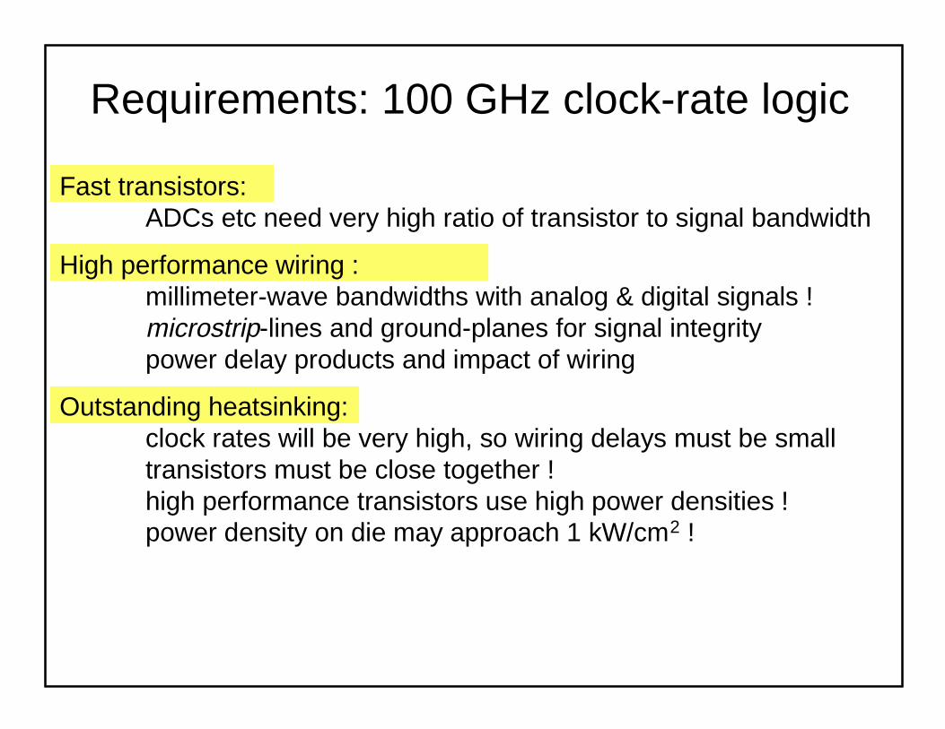
Requirements: 100 GHz clock-rate logic
Fast transistors:ADCs etc need very high ratio of transistor to signal bandwidth
High performance wiring :millimeter-wave bandwidths with analog & digital signals !microstrip-lines and ground-planes for signal integritypower delay products and impact of wiring
Outstanding heatsinking:clock rates will be very high, so wiring delays must be smalltransistors must be close together !high performance transistors use high power densities !power density on die may approach 1 kW/cm2 !

state of the art

Devices and Simple ICs: State of Art, 1999


0.1
1.0
10.0
100.0
Dec-80 Dec-85 Dec-90 Dec-95 Dec-00
Div
ider
Fre
qu
ency
(G
Hz)
III-V HBTSi BJTSiGe HBTFET/HEMTCMOS
Benchmark: master-slave flip-flop configured as 2:1 static frequency dividerSource: M Sokolich, HRL. CMOS Data from Rodwell, UCSB
Logic Speed: III-V vs. Silicon
0.1 um 0.15 um
0.5 um
2 um

HBTperformance


Current-gain cutoff frequency in HBTs
+++++= collex
Ebc
Ejecollectorbase RR
qI
kTC
qI
kTC
fττ
π τ2
1
nbbase DT 22≈τ satccollector vT 2≈τ
Collector velocities can be high: velocity overshoot in InGaAsBase bandgap grading reduces transit time substantiallyRC terms quite important for > 200 GHz ft devices


transferred-substrate HBTs


0
200
400
600
800
1000
0 0.5 1 1.5
f max
, G
Hz
emitter width, microns
Transferred-Substrate HBTs: A Scalable HBT Technology
• Collector capacitance reduces with scaling:• Bandwidth increases rapidly with scaling:
ecb WC ∝
eWf 1max ∝
Ohmics base m .01 µ
Ohmics base m 5.0 µ


Transfer of Entire 2” HBT MMIC Wafer

Transferred-Substrate Heterojunction Bipolar Transistor
0.25 µm devices should obtain ~1000 GHz fmax
Device with 0.6 µm emitter & 1.8 µm collectorextrapolated fmax at instrument limits, >400 GHz
0
5
10
15
20
25
30
35
1 10 100
Gai
ns, d
B
Frequency, GHz
fmax
=470 GHz
fτ=215 GHz
Mason’sGain, U
H21
(?)

Transit times: HBT with 2kT base grading
0
0.2
0.4
0.6
0.8
1
1.2
0 0.1 0.2 0.3 0.4 0.5 0.6
1/2
πfτ (
ps)
1/Ic (1/mA)
0.51 ps
2000 Å InGaAs collector400 Å InGaAs base, 2kT bandgap grading
ps 045.0
ps 065.0
ps 114.0
ps 41.0
=
===+
mcb
mje
cbex
cb
gC
gC
CR
ττ
ps 634.0 total =GHz 252=τf

SEM Photomicrographs of Deep-submicron HBTs
0.15 µm emitter
0.15 µm emitter base junction 0.4 µm collector

0
5
10
15
20
25
100 1000
Gai
ns, d
B
Frequency. GHz
Mason’s gain, U
MSG, common emitter
MSG,common base
H21
, common emitterfmax
= 820 GHz
Submicron Transferred-Substrate HBT
0.4 µm x 6 µm emitter, 0.4 µm x 10 µm collector

0
5
10
15
20
25
30
100 1000
Gai
ns, d
B
Frequency, GHz
Mason’s gain, U
H21
fmax
= 805 GHz fτ = 147 GHz
Transferred-Substrate HBT: Stepper Lithography
0.4 µm emitter, ~0.7 µm collector

Proposed THz-Bandwidth HBT ?
1) regrown P+++ InGaAs extrinsic base --> ultra-low-resistance 2) 0.05 µm wide emitter --> ultra low base spreading resistance3) 0.05 µm wide collector --> ultra low collector capacitance4) 100 Å, carbon-doped graded base --> 0.05 ps transit time5) 1kÅ thick InP collector --> 0.1 ps transit time.
Projected Performance:
Transistor with 500 GHz ft, 1500 GHz fmax
1
2
3
4
5
deep submicron transferred-substrateregrown-base HBT

The wiringenvironment for
100 GHz ICs

Why is Improved Wiring Essential?
ground return loops createinductance
Wire bond createsground bounce betweenIC & package
30 GHz M/S D-FF in UCSB - mesa HBT technology
Ground loops & wire bonds:degrade circuit & packaged IC performance

> 100 GHz CPW ICs: severe crosstalk & ground bounce
70-220 GHz network analyzer chipfor active probe
4-channel 100 Gb/s diode-based DMUX1-180 GHz HEMT amplifier (with HRL)
active probes for 70-220 GHz network analysis
O. Wohlgemuth: Fraunhofer / UCSBO. Wohlgemuth: Fraunhofer / UCSB
B. Agarwal UCSB, M. Matloubian, HRL
R. P
ulle
la, U
CS
B

Coplanar Waveguide and Ground-Bounce
Bond wire inductance resonates with through-wafer capacitance at 5-20 GHz

A D C dig ita lsec tions
inpu tbuffe r
ground re turncurren ts
Lground
∆Ving roundbounceno ise
Ground Bound Noise in ADCs
Ground bounce noise must be ~100 dB below full-scale inputDifferential input will partly suppress ground noise coupling
~ 30 to 40 dB common-mode rejection feasibleCMRR insufficient to obtain 100 dB SNR
Eliminate ground bounce noise by good IC grounding
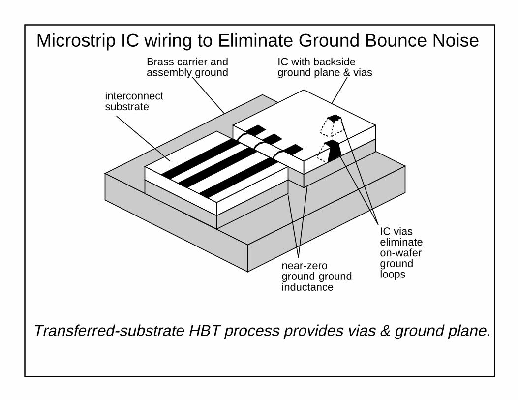
Microstrip IC wiring to Eliminate Ground Bounce NoiseBrass carrier andassembly ground
interconnectsubstrate
IC with backsideground plane & vias
near-zeroground-groundinductance
IC viaseliminateon-wafergroundloops
Transferred-substrate HBT process provides vias & ground plane.

The microstrip via inductance problem
12 pH via inductance for 100 micron MIMIC substrate
j7.5 Ohms at 100 GHz, j15 Ohms at 200 GHz
A formidable difficulty for > 100 GHz IC design
At 100 um substrate thickness, via spacing must be > 100 um
Solutions include “masterslice”, flip-chip, substrate transfer


0
10
20
30
40
50
60
70
80
0 20 40 60 80 100
pow
er s
uppl
y im
peda
nce,
Ohm
s
Frequency (GHz)
On-wafer power distribution for 100 GHz logic
supply will resonate: must prevent during design

Standard cell showing power busses

Deep submicron HBT logic: low power ?
Device sized for 100 Ω load: (200 mV ECL logic swing) 0.15 µm x 6 µm emitter peak speed at 2 mA bias
Shorter stripe length device: 0.15 µm x 0.5 µm emitter peak speed at 150 µA bias
Small device is low-power but cannot drive 100 Ω line.drives line with mismatched impedance: capacitancelower power at higher (wiring-limited) delay
fast low-power logic requires low-voltage-swing-logic

Power-delay product in interconnect limit
bipolar logic (static power)
( ) logic2/1 VVCTP ccwirepropgate ∆=
( ) logic2/1/ VVCfP ccwireclockgate ∆=
CMOS logic (dynamic power)
( ) ~1−clockprop fT number gates between latches
For fast, low-power logic: reduce logicVVcc ∆

The Interconnect Limit and Logic Gate Design
I2I1
Q1aQ1b
Q2a Q2b
RL RL
I1
Av =RL
2kT qI2
=I2 RL
2kT q=
∆Vlogic
2kT q
Volta ge Gain mus t be >> 1
∆Vlogic = 10 • (kT / q)
PgateTgate = 1 2( )Vcc∆VlogicCwire
So:
But:
PgateTgate = 1 2( )(1.5 Volt) (10 •kT / q)Cwire
(power•delay) is constra ined by interconnects
a fast trans is tor doesn't result in a fas t IC
conclusion: a better circuit design is needed
Similar derivation for CMOS (Meindl, Proc IEEE, 1995)

+=∆
bias
switched
I
I
q
kTV 1lnlogic
microwave DDS IC effort:2000 HBTs @ 50-100 GHz clockdissipation is severe issue
Solution (?):small HBTs + low-voltage logic
Principle:low-impedance input current buffer
Challenge:not increasing transistor count

Power Density in 100 GHz logic
Transistors tightly packed to minimize wire delays
105 W/cm2 HBT junction power density.
~103 W/cm2 power density on-chip
--> 75 C temperature rise in 500 µm substrate.
Solutions:thin substrate to < 100 µmreplace semiconductor with metal

0Z0Z
Q
Q
D
C
PLL
Optical vs Electrical Interconnects in Thermal Noise Limit
0Z
0Ioin
ZZ =
Q
Q
D
C
PLL
0I
oinZZ =
nW3Joule/Bit103 192min =⋅== − BkTFBQP
10 Gb/s
Shannon’s limit),2ln(
Binary Antipodal Modulation,36
Q
Q
0Z
W2// 2 µ== ooptical ZkTFBQqhvPΩ= 5000Z
10 Gb/s
Optical receivers are much less sensitive (square law!)
2
2

0Z0Z
Q
Q
D
C0Z
0I
0I
10 Gb/s
10 Gb/s
Lo RIV =∆0ZRL >>
0ZZin =
Q
Q
D
C
Lo RIV =∆RL
Optical vs. Electrical Interconnects:Minimum Signal Amplitude (EMI Tolerance) Limit
Required currents are similar...

So why use optical interconnects ?
Optical fibers are cheapmicrowave cables, connectors, are expensivebut lasers, modulators, detectors must be made cheap
Optical fibers have very low lossmicrowave cables have high skin effect lossesbut lasers, modulators have coupling loss
Optical fibers are compactthin electrical conductors have very high lossesmulti-pin packages must use thin, lossy, conductors
Fiber optics is advantageousbecause optical fibers have very low attenuation

Loss of Coaxial Cable
0.01
0.1
1
10
1 10 100 1000
Atte
nuat
ion,
dB
/met
er
Frequency, GHz
10 mm cable:0.7 dB/m at10 GHz cutoff
3 mm cable:3.1 dB/m at33 GHz cutoff
1 mm cable:14 dB/m at 100 GHz cutoff
1.2=rε 4103)tan( −⋅=δ
( ) 12/1)/2( requiresn propagatio mode-Single −− +⋅≤ outerinnerr DDcf επ2/32/1 Loss / lossSkin fDf skininnerskin ∝→∝ αα

circuit results:transferred-substrate
technology

Transferred-Substrate HBT Integrated Circuits
7 dB, 5-80 GHz distributed amplifier
11 dB, 50+ GHz AGC / limiting amplifier 16 dB, DC-60 GHz amplifier
6.7 dB, DC-85 GHz amplifier

Darlington Amplifier - 360 GHz GBW
• 15.6 dB DC gain• Interpolated 3dB bandwidth of 60 GHz• 360 GHz gain-bandwidth product
-15
-10
-5
0
5
10
15
20
0 20 40 60 80 100
dB
Frequency, GHz
S21
S11
S22

0
2
4
6
8
10
0 20 40 60 80 100
For
war
d G
ain,
S21
, dB
Frequency, GHz
6.7 dB, 85 GHz Mirror Darlington Amplifier
• 6.7 dB DC gain• 3 dB bandwidth of 85 GHz• fτ-doubler (mirror Darlington) configuration

> 66 GHz HBT master-slave flip-flop
Objectives: 100 + GHz logic
Approach:transferred-substrate HBTsefficient circuit design
Simulations:95 GHz clock rate in SPICE
Measurements:operation to 66 GHz limit of test setupnow building 75-110 GHz test setup
33.0 GHz static divider output at 66.0 GHz input
-100
-80
-60
-40
-20
0
0 50 100 150 200
divi
der
out
put
, mV
time , ps

> 66 GHz HBT master-slave flip-flop

Fiber OpticICsnot yet tested(design 40 Gb/s)
AGC / limiting amplifier CML decision circuit
PIN / transimpedance amplifier

Delta-Sigma ADC (300 HBTs)

Fast ICs for fast interconnectsFast ICs needing fast interconnects
ICs for GHz communications:Optical fiber transmission to, beyond 40 Gb/s
with electronic data switchingmillimeter-wave (60/90/180 GHz) wireless networks
at mm-wave, bandwidth is cheap & plentiful…but the hardware must become cheap
ADCs, DACs for digital processing of RF signals
Challenges for fast ICsFast transistors: scaling is keyWiring environment: signal, ground and power integrityInterconnect-limited power-delay productsManaging high dissipated power densities


![EU2017MT BLUEMED Presentation Petrioli...Opportunites and Challenges ! UnderwaterInternet[of Things] allows*to*interconnect*underwater* sensors, underwater*robo8cs*technologies, enablingrealmedata,](https://static.fdocuments.net/doc/165x107/604e2c8f27fb8d15dc1e7c34/eu2017mt-bluemed-presentation-opportunites-and-challenges-underwaterinternetof.jpg)