Development of HOM Absorber for KEK B-Factory SC...
19
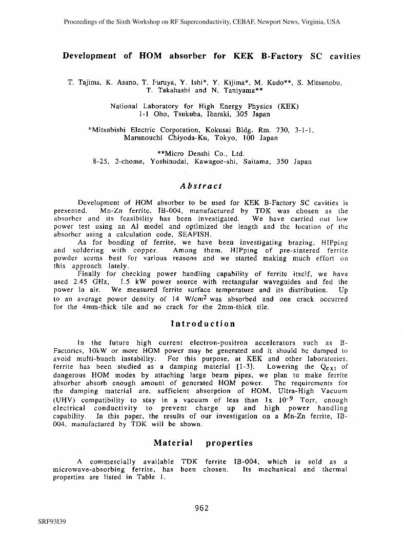
Development of HOM absorber for KEK B-Factory SC cavities T. Tajima, K. Asano, T. Furuya, Y. Ishi*, Y. Kijima*, M. Kudo**, S. Mitsunobu, T. Takahashi and N. Taniyama*" National Laboratory for High Energy Physics (KEK) 1-1 Oho, Tsukuba, Ibaraki, 305 Japan "Mitsubishi Electric Corporation, Kokusai Bldg. Rm. 730, 3-1-1, Marunouchi Chiyoda-Ku, Tokyo, 100 Japan **Micro Denshi Co., Ltd. 8-25, 2-chome, Yoshinodai, Kawagoe-shi, Saitama, 350 Japan Abstract Development of HOM absorber to be used for KEK B-Factory SC cavities is presented. Mn-Zn ferrite, IB-004, manufactured by TDK was chosen as the absorber and its feasibility has been investigated. We have carried out low power test using an A1 model and optimized the length and the location of the absorber using a calculation code, SEAFISH. As for bonding of ferrite, we have been investigating brazing, HIPping and soldering with copper. Among them, HIPping of pre-sintered ferrite powder seems best for various reasons and we started making much effort 011 this approach lately. Finally for checking power handling capability of ferrite itself, we have used 2.45 GHz, 1.5 kW power source with rectangular waveguides and fed the power in air. We measured ferrite surface temperature and its distribution. Up to an average power density of 14 w/cm2 was absorbed and one crack occurred for the 4mm-thick tile and no crack for the 2mm-thick tile. Introduction In the future high current electron-positron accelerators such as R- Factories, lOkW or more HOM power may be generated and it should be damped to avoid multi-bunch instability. For this purpose, at KEK and other laboratories, ferrite has been studied as a damping material [I-31. Lowering the Qext of dangerous HOM modes by attaching large beam pipes, we plan to make ferrite absorber absorb enough amount of generated HOM power. The requirements for the damping material are, sufficient absorption of HOM, Ultra-High Vacuum (UHV) compatibility to stay in a vacuum of less than lx Torr, enough electrical conductivity to prevent charge up and high power handling capability. In this paper, the results of our investigation on a Mn-Zn ferrite, IB- 004, manufactured by TDK will be shown. Material properties A commercially available TDK ferrite IB-004, which is sold as a microwave-absorbing ferrite, has been chosen. Its mechanical and thermal properties are listed in Table 1. Proceedings of the Sixth Workshop on RF Superconductivity, CEBAF, Newport News, Virginia, USA SRF93I39
Transcript of Development of HOM Absorber for KEK B-Factory SC...
Development of HOM absorber for KEK B-Factory SC cavities
T. Tajima, K. Asano, T. Furuya, Y. Ishi*, Y. Kijima*, M. Kudo**, S. Mitsunobu, T. Takahashi and N. Taniyama*"
National Laboratory for High Energy Physics (KEK) 1-1 Oho, Tsukuba, Ibaraki, 305 Japan
"Mitsubishi Electric Corporation, Kokusai Bldg. Rm. 730, 3-1-1, Marunouchi Chiyoda-Ku, Tokyo, 100 Japan
**Micro Denshi Co., Ltd. 8-25, 2-chome, Yoshinodai, Kawagoe-shi, Saitama, 350 Japan
A b s t r a c t
Development of HOM absorber to be used for KEK B-Factory SC cavities is presented. Mn-Zn ferrite, IB-004, manufactured by TDK was chosen as the absorber and its feasibility has been investigated. We have carried out low power test using an A1 model and optimized the length and the location of the absorber using a calculation code, SEAFISH.
As for bonding of ferrite, we have been investigating brazing, HIPping and soldering with copper. Among them, HIPping of pre-sintered ferrite powder seems best for various reasons and we started making much effort 011
this approach lately. Finally for checking power handling capability of ferrite itself, we have
used 2.45 GHz, 1.5 kW power source with rectangular waveguides and fed the power in air. We measured ferrite surface temperature and its distribution. Up to an average power density of 14 w/cm2 was absorbed and one crack occurred for the 4mm-thick tile and no crack for the 2mm-thick tile.
I n t r o d u c t i o n
In the future high current electron-positron accelerators such as R - Factories, lOkW or more HOM power may be generated and it should be damped to avoid multi-bunch instability. For this purpose, at KEK and other laboratories, ferrite has been studied as a damping material [I-31. Lowering the Qext of dangerous HOM modes by attaching large beam pipes, we plan to make ferrite absorber absorb enough amount of generated HOM power. The requirements for the damping material are, sufficient absorption of HOM, Ultra-High Vacuum (UHV) compatibility to stay in a vacuum of less than l x Torr, enough electr ical conductivi ty to prevent charge up and high power handling capability. In this paper, the results of our investigation on a Mn-Zn ferrite, IB- 004, manufactured by TDK will be shown.
Material properties
A commercially available TDK ferrite IB-004, which is sold as a microwave-absorbing ferrite, has been chosen. I ts mechanical and thermal properties are listed in Table 1.
Proceedings of the Sixth Workshop on RF Superconductivity, CEBAF, Newport News, Virginia, USA
SRF93I39
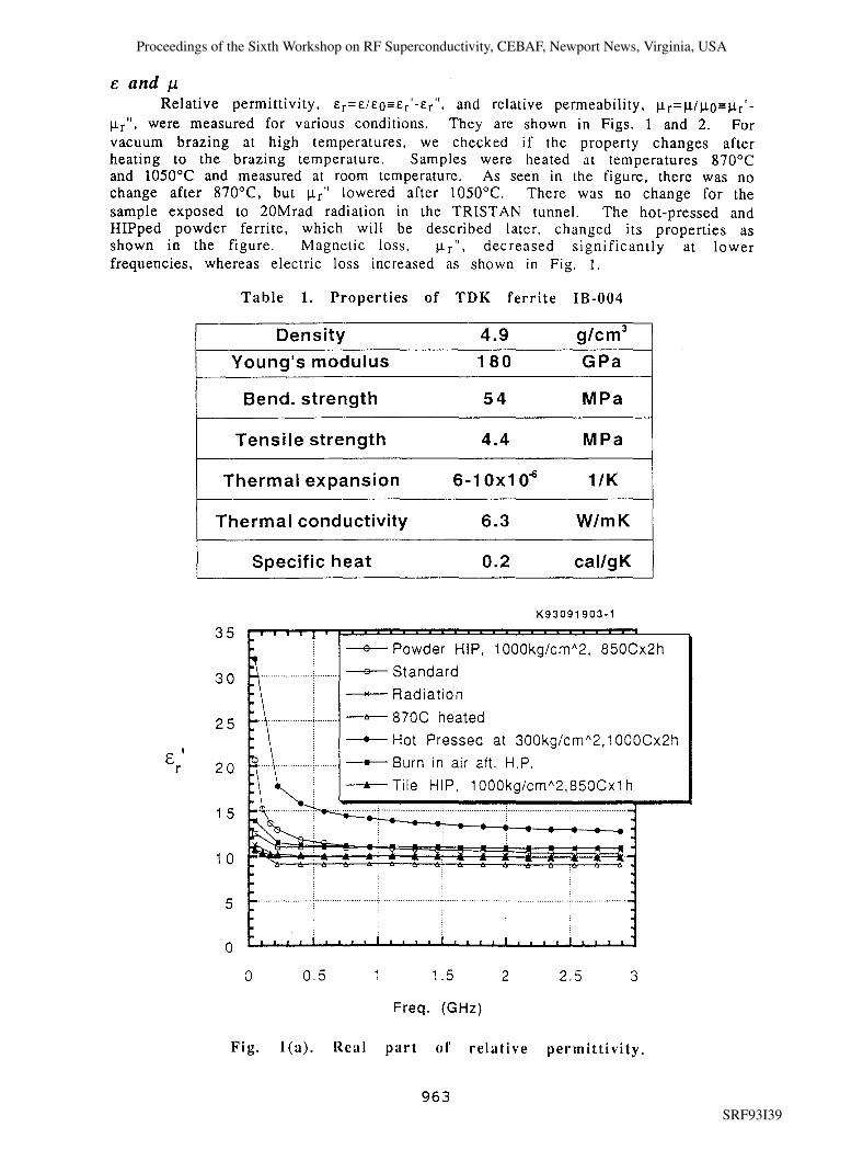
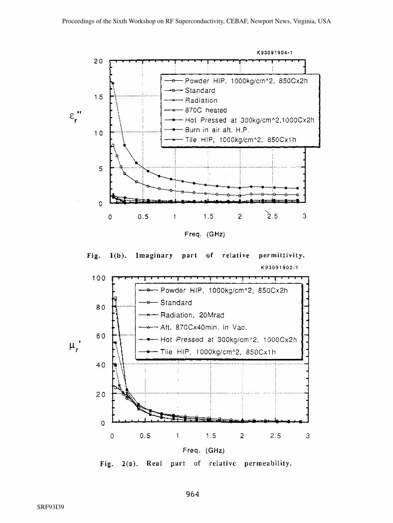
E and p Relative permittivity, E ~ = E / E o ~ E ~ ' - E ~ " , and relative permeability, p r = p / p 0 = p r 1 -
pr", were measured for various conditions. They are shown in Figs. 1 and 2. For vacuum brazing at high temperatures, we checked if the property changes after heating to the brazing temperature. Samples were heated at temperatures 870°C and 1050°C and measured at room temperature. As seen in the figure, there was no change after 870°C, but pr" lowered after 1050°C. There was no change for the sample exposed to 20Mrad radiation in the TRISTAN tunnel. The hot-pressed and HIPped powder ferrite, which will be described later, changed its properties as shown in the figure. Magnetic loss, p r " , decreased significantly at lower frequencies, whereas electric loss increased as shown in Fig. 1.
T a b l e 1. P rope r t i e s of T D K f e r r i t e IB-004
Density 4.9 glcm3 -
Young's modulus 180 GPa
Bend. strength 5 4 MPa
Tensile strength 4.4 MPa
Thermal expansion 6-1 0x1 o6 11K
Thermal conductivity 6.3 Wlm K
Specific heat 0.2 callg K
0
0 0 .5 1 1.5 2 2 . 5 3
Freq. (GHz)
Fig . l ( a ) . Real p a r t o f re la t ive pe rmi t t i v i ty .
Proceedings of the Sixth Workshop on RF Superconductivity, CEBAF, Newport News, Virginia, USA
SRF93I39
l " " 1 " " i " " l " " l " "
*Powder HIP, 1000kglcmA2, 850Cx2h - Standard - Radiation - 870C heated -- Hot Pressed at 300kglcmA2,1 000Cx2h -- Burn in air aft. H.P. - Tile HIP, 1 000kg/cmA2, 850Cxl h
Freq. (GHz)
F i g . l ( b ) . I m a g i n a r y p a r t of r e l a t i v e p e r m i t t i v i t y .
Kg3091 902-1
1 0 0
0
0 0 .5 1 1.5 2 2 .5 3
Freq. (GHz)
Fig. 2 ( a ) . Real part of re la t ive p e r m e a l ~ i l i t y .
- Standard - Radiation, 20Mrad - Aft. 870Cx40min. in Vac. - Hot Pressed at 300kglcmA2, 1000Cx2h
Proceedings of the Sixth Workshop on RF Superconductivity, CEBAF, Newport News, Virginia, USA
SRF93I39
Kg3091 901-1
6 0 - Standard 5 0 - Rad~at~on, 20Mrad - Aft. 870Cx40m1n. In Vac. 4 0 - Hot Pressed at 300kg/cmA2,1 000Cx2h
' 3 0
2 0
1 0
0
Freq. (GHz)
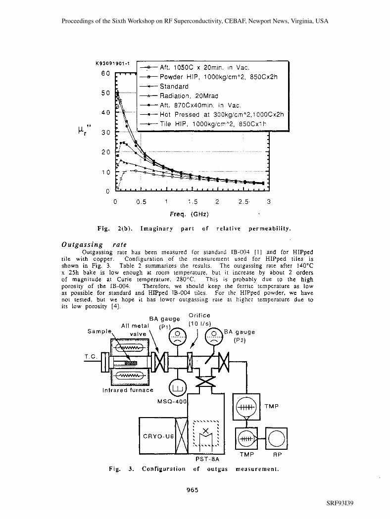
Fig. 2(b). I m a g i n a r y p a r t of r e l a t i ve pe rmeab i l i t y .
Outgass ing rate Outgassing rate has been measured for standard IB-004 [ I ] and for HIPped
tile with copper. Configuration of the measurement used for HIPped tiles is shown in Fig. 3. Table 2 summarizes the results. The outgassing rate after 140°C x 25h bake is low enough at room temperature, but i t increase by about 2 orders of magnitude at Curie temperature, 280°C. This is probably due to the high porosity of the IB-004. Therefore, we should keep the ferrite temperature as low as possible for standard and HIPped IB-004 tiles. For the HIPped powder, we have not tested, but we hope it has lower outgassing rate at higher temperature due to its low porosity [4].
Fig. 3. Conf igu ra t ion of o u t g a s n ieasurement .
965
Proceedings of the Sixth Workshop on RF Superconductivity, CEBAF, Newport News, Virginia, USA
SRF93I39

Table 2. Outgassing rate of IR-004.
I for 230 hours 1
S a m p l e I C o n d i t i o n
S t a n d a r d I B - 0 0 4
S t a n d a r d I B - 0 0 4 HIPped t i le o n copper
HIPped t i l e o n copper
Optimization of ferrite length and location with SEAFISH
O u t g a s s i n g r a t e
SEAFISH is a complex version of SUPERFISH, in which lossy materials such as ferrite can be included [2]. The outputs are resonant frequency, Qext and field pattern. The dependencies of location, ferrite length and thickness on Qext were studied for TMOll mode since this mode is expected to generate major power. In the following figures, Qex t is written as QL because Qext is almost the same as loaded Q, QL, because Qext is much lower than unloaded Q, Qo. Also, the E and p used in the calculation are the ones for standard IB-004.
Figures 4 shows the Q as a function of the distance from the end of taper as shown in the figure in the case of 6cm long ferrite, whereas Fig. 5 shows the same graph for 15cm long ferrite. In both figures, thickness is another
a t room t e m p e r a t u r e a f t er 140Cx24h bake
whi le heat ing at 245C a t room t e m p e r a t u r e a f t er 140Cx24h bake
whi le heating at 280C
parameter, e.g. 3t means 3mm-thick ferrite layer. Figure 6 shows the Q as a function of length for the ferrite located 17cm
away from the taper. As one can see, for 2mm-thick case, the Q is much more sensitive to the ferrite thickness the case of 4mm and 6mm. From the ferrite length should be longer than 15cm for the ferrite equal to or thicker than 2mm.
Figure 7 shows the Q as a function of p r " in the case that ferrite thickness is 4mm, length is 15cm and distance from the taper is 19cm. As one can see, the Q does not change much for the p" greater than about 5. Other parameters such as E', E " and p ' are found to have little influence on the Q.
Figure 8 shows the Q's as functions of ferrite location and length. As one can see, the minimum Q was found to be at the point where ferrite length is 15cm and distance from the taper is 19cm.
Figure 9 shows the field patterns when the ferrite is set at the optimized pos i t ion .
(Torr 11s c m 2 ) 5 x 1 0 - l 1
2 ~ 1 0 - 9 1 . 4 - 2 . 5 ~ 1 0 - ~ ~
2 . 2 ~ 1 0 - 9
Low power test with A1 model
Figure 10 shows the comparison between with and without ferrite absorber. As one can see, most of the HOM's are sufficiently damped with the absorber. This test was performed with an A1 model cavity and HP8720C network a n a l y z e r .
Table 3 shows the results of measurements with the results from SEAFISH and URMEL. The measurements were sometimes difficult because of the overlap of adjacent modes. Nevertheless, as onc can see, they were in good agreement with calculations.
Proceedings of the Sixth Workshop on RF Superconductivity, CEBAF, Newport News, Virginia, USA
SRF93I39
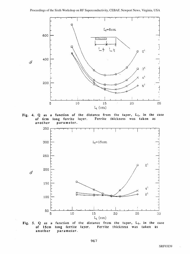
Fig. 4. Q as a function of the distance from the taper, Lt, in the case of 6cm long ferrite layer. Ferrite thickness was taken as a n o t h e r p a r a m e t e r .
350
L, (em) Fig. 5. Q as a function of the distance from the taper, L t , in the case
of 15cm long ferrite layer. Ferrite thickness was taken as a n o t h e r p a r a m e t e r .
I l l 1 I I I I I l l 1 I I I I - - - - Lf=6cm - - - - - - - -
2' -
- -
- - - -
- 3' -
- -
- 4' -
- - 6 - -
- d
- I I I I I I I I I I I I I l l 1
-
Proceedings of the Sixth Workshop on RF Superconductivity, CEBAF, Newport News, Virginia, USA
SRF93I39

Fig. 6. Q a s a funct ion of fe r r i t e length, Lf, when t h e d i s t ance f r o m t h e t a p e r is 17cm. Thickness was t aken a s a n o t h e r pa rame te r .
Fig. 7. Q as a funct ion of the i ~ n a g i n a r y p a r t of the relat ive p e r m e a b i l i t y , p", in the case t ha t f e r r i t e thickness is 4mm, f e r r i t e l ength is 15cm a n d f e r r i t e position is 19cm away f rom the taper .
Proceedings of the Sixth Workshop on RF Superconductivity, CEBAF, Newport News, Virginia, USA
SRF93I39
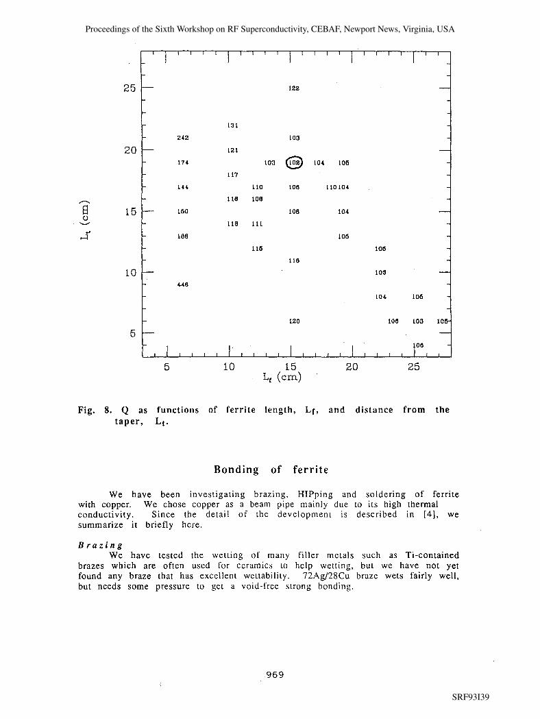
Fig. 8. Q as funct ions of f e r r i t e length, Lf, and d is tance f r o m t h e t a p e r , Lt.
Bonding of ferrite
We have been investigating brazing, HIPping and soldering of ferrite with copper. We chose copper as a beam pipe mainly due to its high thermal conductivity. Since the detail of the development is described in [4], we summarize it briefly here.
B r a z i n g We have tested the wetting of many filler metals such as Ti-contained
brazes which are often used for ceramics to help wetting, but we have not yet found any braze that has excellent wettability. 72Agf28Cu braze wets fairly well, but needs some pressure to get a void-free strong bonding.
Proceedings of the Sixth Workshop on RF Superconductivity, CEBAF, Newport News, Virginia, USA
SRF93I39
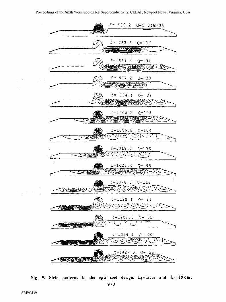
Fig. 9. Field patterns in the optimized design, Lf=15cm and L t = 1 9 c m .
970
Proceedings of the Sixth Workshop on RF Superconductivity, CEBAF, Newport News, Virginia, USA
SRF93I39

1 2 log M A G , 10 d B / R E F - 6 5 d B
W i t h o u t D a m p e r
C H I
START 0.500 000 000 G H Z STOP 1.200 000 000 G H z
Fig. 10. Mode darnping test with Al model cavity.
W i t h D a m p e r
Proceedings of the Sixth Workshop on RF Superconductivity, CEBAF, Newport News, Virginia, USA
SRF93I39
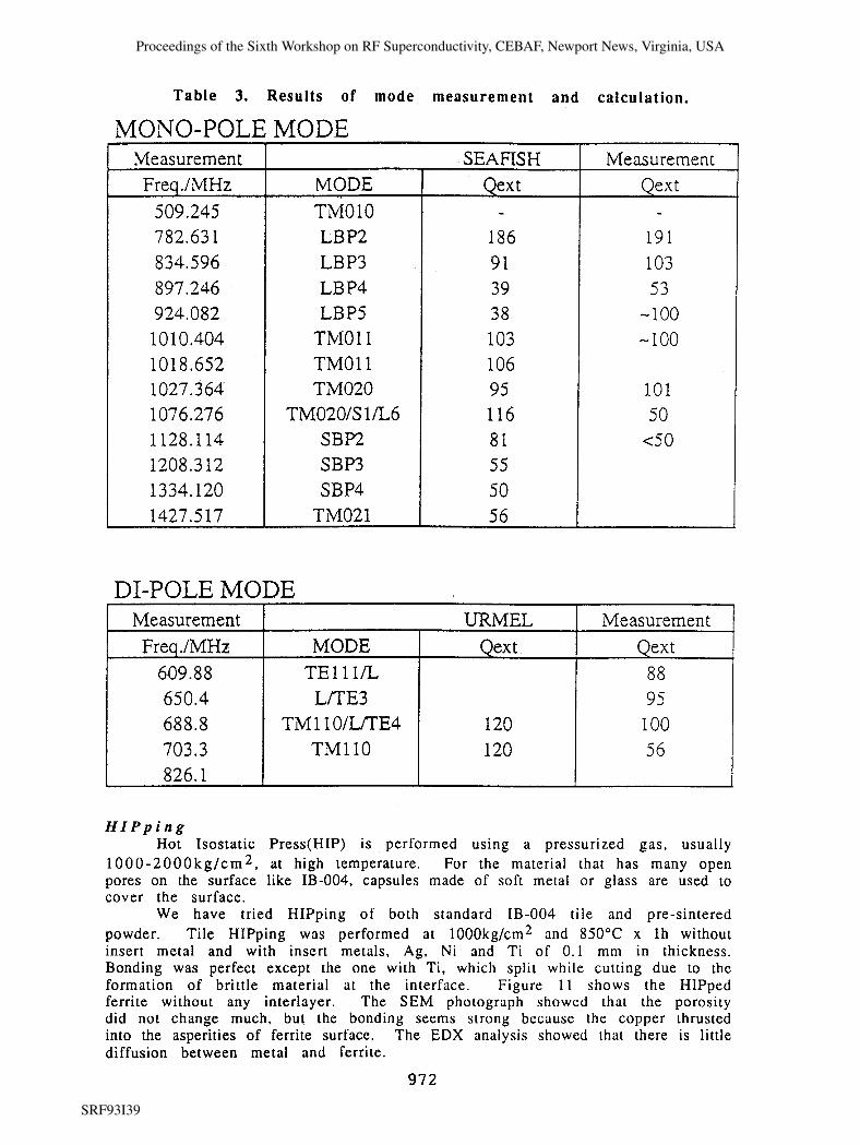
Table 3. Results of mode measurement and calculation.
MONO-POLE MODE Measurement Frea ./MHz
DI-POLE MODE
Measurement Qex t
-
191 103 53
- 100 -100
101 50
4 0
SEAFISH
H I P p i n g Hot Isostatic Press(H1P) is performed using a pressurized gas, usually
1 0 0 0 - 2 0 0 0 k g / c m 2 , at high temperature. For the material that has many open pores on the surface like IB-004, capsules made of soft metal or glass are used to cover the surface.
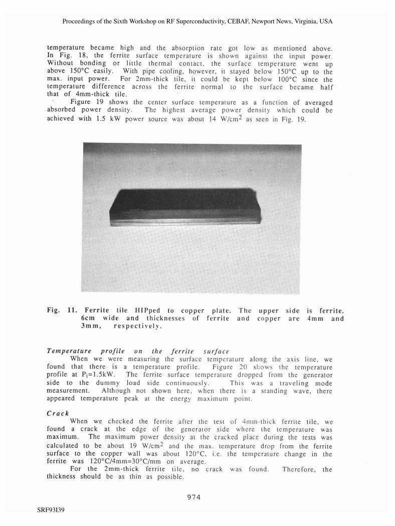
We have tried HIPping of both standard IB-004 tile and pre-sintered powder. Tile HIPping was performed at 1000kg/cm2 and 850°C x l h without insert metal and with insert metals, Ag, Ni and Ti of 0.1 mm in thickness. Bonding was perfect except the one with Ti, which split while cutting due to the formation of brittle material at the interlace. Figure 11 shows the HlPped ferrite without any interlayer. The SEM photograph showed that the porosity did not change much, but the bonding seems strong because the copper thrusted into the asperities of ferrite surface. The EDX analysis showed that there is little diffusion between metal and ferrite.
PIODE TMO10 LBP2 LBP3 LB P4 LBP5
ThdOll TMO11 TM020
TM020lS 1/L6 SBF2 SBP3 SBP4
TM021
Measurement Freq ./MHz
609.88 650.4 688.8 703.3 826.1
Qex t -
186 91 39 38 103 106 95 116 8 1 55 50 56
Measurement Qex t
88 95 100 56
URMEL MODE
TE1111L LlTE3
TM 1 1 OILl'TE4 TM110
Qext
120 120
Proceedings of the Sixth Workshop on RF Superconductivity, CEBAF, Newport News, Virginia, USA
SRF93I39
Another approach of HIPping is to use ferrite powder. There are several advantages, 1) cylindrical layer can be formed on the inner surface of the pipe, 2) porosity of ferrite can be reduced, thus lowgring the outgassing rate and 3) thermal conductivity can be improved. One drawback was thought to be a reduction of magnetic loss, but i t was found to be small enough at the frequencies of interest as described below.
Before HIPping powder, we tried to hot-press pre-sintered ferrite powder with carbon press in vacuum at 300kg/cm2 and 1000°C x 2h to check if the magnetic loss decreases. As shown in Figs. 1 and 2, the magnetic loss, i.e. p", did not change at the frequencies of interest, i.e. lGHz and higher, although it decreased drastically at lower frequencies. Powder HIPping on the inner surface of a 109mm-diam. copper pipe has started lately. First try was unsuccessful seemingly due to a pin-hole created while HIPping because the capsule did not shrink as we expected. In the first try, due to the packing by hand, the packing density of the powder was 40 % of the density of hot-pressed powder, which is much less than the desired packing density for HIPping, 60-70 %. The second try is now under way, in which we improved the packing density to 47 % by mechanical press packing and the way of sealing capsule.
S o l d e r i n g Since usual solder does not wet well with ferrite, we applied ultrasonic
soldering, in which the solder tip vibrates and helps wetting of the solder. Also, the solder itself is specially manufactured for better wetting against oxides. In the first try with a solder named Cerasolzer W123 and W297 [5], it wetted well with ferrite and copper. We used this method for 1 atm high power test as will be mentioned below. Despite the good wettability, it split in the solder when being cut for microscopic inspection. We think it is because the soldering was done in air and the solder was oxidized to form a weak layer in the solder. Another problem with this solder is that it contains considerable amount of zinc and its vapor pressure at elevated temperature is so high that it will be harmful to UHV. In the next test we will use a solder having lower content of zinc and in the atmosphere of either Ar or N2.
High power test
To know the power handling capability of IB-004, we have performed sample tests using 6cm x 6cm x 2-4mm tiles with 2.45GHz 1.5kW power source in air. The configuration of the test setup is shown in Fig. 12. The ferrite tile was set in a rectangular waveguide as shown in Fig. 13. To monitor the ferrite surface temperature, we made a Smm-wide and 7cm long slit on the opposite wall and IR thermometer was used as shown in Fig. 14. The dummy load at the end was adjusted so that there is no reflection from it.
At first we measured the absorbed power without bonding the ferrite and without any cooling. Then we bonded it with Al tape and cooled it by the water flowing in the 114" copper pipe soldered as shown in Fig. 13. Finally, we soldered the ferrite in the way mentioned above to reduce the thermal resistance between copper and ferrite. Figure 15 shows the ultrasonically soldered ferrite and high power test setup. In the data shown here, the cooling water flow rate was 7.5 literlmin. and the inlet temperature was 20°C.
Figure 16 shows the absorption rate, i.e. ratio of absorbed power to the input power, as a function of center surface temperature. As one can see, the absorption rate decreased with temperature and became about 10 % at Curie temperature. This decrease, however, is little until about 100°C, i.e. the low power characteristics shown above will be valid until approximately 100°C.
Figure 17 shows the average absorbed power density as a function of input power. The absorbed power for the unbonded ferrite did not increase much at the input power higher than about 400W because the ferrite
Proceedings of the Sixth Workshop on RF Superconductivity, CEBAF, Newport News, Virginia, USA
SRF93I39
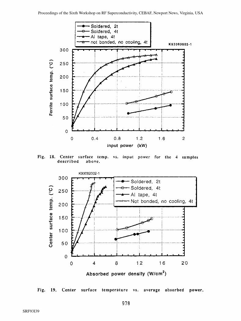
temperature became high and the absorption rate got low as mentioned above. In Fig. 18, the ferrite surface tempcrature is shown against the input power. Without bonding o r little thermal contact. the surfacc temperature went up above 150°C easily. With pipe cooling, however, i t stayed below 150°C.up to the max. input power. For 2mm-thick tile, i t could be kept below 100°C since the temperature difference across the ferrite normal to the surface became half that of 4mm-thick tile.
Figure 19 shows the center surface temperature as a function of averaged absorbed power density. The highest average power density which could be achieved with 1.5 kW power source was about 14 w/cm2 as seen in Fig. 19.
Fig. 11. F e r r i t e ti le H lPped to coppe r plate . T h e u p p e r s ide is fe r r i te . 6cm wide a n d thicknesses of f e r r i t e a n d c o p p e r a r e 4mm a n d 3 m m , r e s p e c t i v e l y .
Temperature profi le on the ferri te surface When we were measuring the surface tempcrature along the axis line, we
found that there is a temperature profile. Figure 20 shows the temperature profile at P,=I.SkW. The ferrite surface temperature dropped from the generator side to the dummy load side continuously. This was a traveling mode measurement. Although not shown here, when there is a standing wave, there appeared temperature peak at the energy maximum point.
C r a c k When we checked the ferrite a f ~ c r the test of 4mm-thick ferrite tile, we
found a crack at the edge of the generalor side where the temperature was maximum. The maximum power density at the cracked place during the tests was calculated to be about 19 w/cm2 and the max. temperature drop from the ferrite surface to the copper wall was about 120°C, i.e. the temperature change in the ferrite was 12OoC/4mm=3OoC/mm on average.
For the 2mm-thick ferrile tilc, no crack was found. Therefore, the thickness should be as thin as possible.
Proceedings of the Sixth Workshop on RF Superconductivity, CEBAF, Newport News, Virginia, USA
SRF93I39

Cooling Cooling Cooling
U Pr A U U
Generator W/ Ferrite
maxi .5kW lsolator 90-95% Pi matching
transmission posts
Fig. 12. Configuration of high power test of a ferrite tile.
Gemerator
I C-
Dummy I load - \
Copper Ferrite (18-004)
\ Cooling water 114" Cu pipe
Fig. 13. Setup of ferrite in a 2.45GHz rectangular waveguide.
Top view
Slit
Temperature
Spotsize monitor
at the slit Minolta TR-0506C
2mmq \ I
Fig. 14. Temperature motlitori~lg of the ferrite surface using IR t h e r m o m e t e r .
Proceedings of the Sixth Workshop on RF Superconductivity, CEBAF, Newport News, Virginia, USA
SRF93I39

Fig. 15. Soldered ferr i te a n d high power test se tup .
Proceedings of the Sixth Workshop on RF Superconductivity, CEBAF, Newport News, Virginia, USA
SRF93I39

50 100 150 200 250 300
Surface temp. at ferrite center ( O C )
Fig. 16. Absorption rate a s a function of center surface temperature.
--e- Soldered, 4t -not bonded, no cooling
. . . . . . . . . . . . . . . . . . . . . . . .
Input power , Pi, (kW)
Fig. 17. Average absorbed power density vs . input power for the 4mm-thick samples of not bonded, bonded with Al tape and so ldered, and the soldered 2mm-thick sample .
Proceedings of the Sixth Workshop on RF Superconductivity, CEBAF, Newport News, Virginia, USA
SRF93I39
-8- Soldered, 2t -+- Soldered, 4t +A1 tape, 4t - not bonded, no cooling, 4t
0 0.4 0.8 1.2 1.6 2
Input power (kW)
Fig. 18. Center surface temp. vs. input power for the 4 samples d e s c r i b e d a b o v e .
Absorbed power density ( w l c m 2 )
Fig. 19. Center surface temperature vs . average absorbed power.
Proceedings of the Sixth Workshop on RF Superconductivity, CEBAF, Newport News, Virginia, USA
SRF93I39

Fig.
K 9 3 0 8 0 6 0 6 - 1 -2t, 7.5 I/min.
I - - 1 1 . 1 1 1 1 . 1 1 1 1 1 1 1 1 1 1 1 1 l l l 1 1 1 1 ,
3 0 - 2 0 - 1 0 0 1 0 2 0 3 0
Position (mm)
20. T e m p e r a t u r e prof i le on the f e r r i t e sur face . T h e i npu t power was 1.5 kW.
C o n c l u s i o n
Development of the HOM absorber for the KEK B-Factory SC cavities was presented. We have been investigating the feasibility of a Mn-Zn microwave- absorbing ferrite IB-004 manufactured by TDK as an HOM absorber. HOM damping capability was confirmed by low power tests with A1 model. Optimization of the location, length and thickness has been done with a calculation code SEAFISH. Outgassing rate at room temperature is sufficiently low, but it increases with temperature drastically. Thus it is necessary to keep ferrite temperature as low as possible.
Bonding of ferrite with copper has been studied with 3 approaches, brazing, HIPping and soldering. Although we have not made a full-scale model yet, each approach is in progress and we hope to be able to have a full-scale load for high power tests soon.
From the high power tests with 2.45 GHz, 1.5kW power source, it has been found that IB-004 standard ferrite of 4mm in thickness suffers a crack at about 19W/cm, which will probably depends on the stress situation in the ferrite. For 2mm-thick ferrite tile, no cracks were found as well as the surface temperature gets low. In this sense, the ferrite layer should be as thin as possible.
A c k n o w l e d g m e n t s
The authors would like to thank K . Saito of ULVAC Corp. for conducting outgass experiment. They also would like to thank I. Campisi, W. Hartung and D. Moffat for their useful discussions. Continuous encouragement of E. Ezura, Y. Kimura, Y. Kojima and S . Kurokawa are greatly appreciated. In addition, useful comments from other group members are acknowledged.
Proceedings of the Sixth Workshop on RF Superconductivity, CEBAF, Newport News, Virginia, USA
SRF93I39

R e f e r e n c e s
[ l ] T. Tajima et a].; KEK Preprint 93-6, presented at the Workshop on Microwave- Absorbing Materials for Accelerators, CEBAF, Feb. 22-24, 1993.
[2] D. Moffat et al.; ibid. [ I ] . [3] R. Boni et al.; ibid. [ I ] . [4] T. Tajima et al.; in this workshop. [S] Products o f Asahi Glass Company.
Proceedings of the Sixth Workshop on RF Superconductivity, CEBAF, Newport News, Virginia, USA
SRF93I39