Development of GaN SSPA for Satellite-Borne Application · High RF Power C-Band Uplink Downlink ......
26
Page 1 of 25 COMPANY PROPRIETARY NOT TO BE REPRODUCED OR DISCLOSED WITHOUT SPECIFIC WRITTEN PERMISSION OF MITSUBISHI ELECTRIC TOKKI SYSTEMS CORPORATION TKE-2010-0906 A MELOS Mitsubishi Electric TOKKI Systems Corporation MELOS Mitsubishi Electric TOKKI Systems Corporation Microelectronics Work Shop 23 Microelectronics Work Shop 23 November 10, 2010 November 10, 2010 Development of GaN SSPA for Satellite-Borne Application Development of GaN SSPA for Satellite-Borne Application
Transcript of Development of GaN SSPA for Satellite-Borne Application · High RF Power C-Band Uplink Downlink ......
Page 1 of 25 COMPANY PROPRIETARY
NOT TO BE REPRODUCED OR DISCLOSED WITHOUT SPECIFIC
WRITTEN PERMISSION OF MITSUBISHI ELECTRIC TOKKI SYSTEMS CORPORATION
TKE-2010-0906 A
MELOS����Mitsubishi Electric TOKKI Systems Corporation
MELOS����Mitsubishi Electric TOKKI Systems Corporation
Microelectronics Work Shop 23Microelectronics Work Shop 23
November 10, 2010November 10, 2010
Development of GaN SSPA for Satellite-Borne Application
Development of GaN SSPA for Satellite-Borne Application

Page 2 of 25 COMPANY PROPRIETARY
NOT TO BE REPRODUCED OR DISCLOSED WITHOUT SPECIFIC
WRITTEN PERMISSION OF MITSUBISHI ELECTRIC TOKKI SYSTEMS CORPORATION
TKE-2010-0906 A
1. The high power amplifier for satellite use
2. GaN device characteristics
3. GaN Device: Achieved Performance
4. GaN SSPA: Achieved Performance
5. Conclusion and Next Target
Table of Contents
Page 3 of 25 COMPANY PROPRIETARY
NOT TO BE REPRODUCED OR DISCLOSED WITHOUT SPECIFIC
WRITTEN PERMISSION OF MITSUBISHI ELECTRIC TOKKI SYSTEMS CORPORATION
TKE-2010-0906 A1. High Power Amplifier1. High Power Amplifier
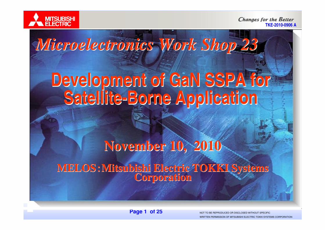
The present situation of the high power amplifier for satellite use
Command Signals
Figure 1-1
Space Segment (Satellite)
Uplink
Telemetry Signals
Downlink ���� Needs
Service Station Interface Station TTC Station
Ground Segment Control Segment
High RF Power
C-Band Uplink Downlink6GHz 4GHz
14GHz 12GHzKu-Band

Page 4 of 25 COMPANY PROPRIETARY
NOT TO BE REPRODUCED OR DISCLOSED WITHOUT SPECIFIC
WRITTEN PERMISSION OF MITSUBISHI ELECTRIC TOKKI SYSTEMS CORPORATION
TKE-2010-0906 A
Figure 1-2 Typical Communication Subsystem in the Communication Satellite
Uplink Downlink
HPA
PFTC
Ch.
HYB
1:3
Ch.
Ch.
Ch.
Ch.
LNA
LNA
LNA
LNA
LNA
PFTC
PFTC
TWT
TWT
TWT
TWT
TWT
TWT
TWT
TWT
CA
BCN
BCN
C
BCN
BCN
C
TC
Tx FIL
TCTx FIL
TC
Tx FIL
FEED
FEED
FEED
HYB
1:4
HYB
1:4
HYB
1:2
CA
D/C
CA
CA
CA
CA
CA
CA
D/C
D/C
D/C
D/C
D/C
D/C
D/C
O-MUX
O-MUX
O-MUX
1. High Power Amplifier1. High Power Amplifier
HPAs are applied to each communication channels
���� Applied many HPAs�Required
Light WeightSmall Footprint
Page 5 of 25 COMPANY PROPRIETARY
NOT TO BE REPRODUCED OR DISCLOSED WITHOUT SPECIFIC
WRITTEN PERMISSION OF MITSUBISHI ELECTRIC TOKKI SYSTEMS CORPORATION
TKE-2010-0906 A
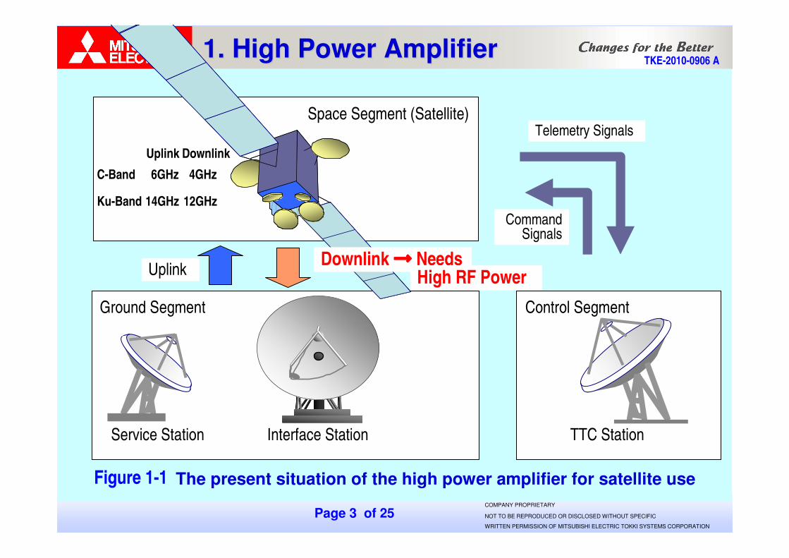
Main Performance :Frequency: L/S/C BandOutput Power:70 to 150 wattsEfficiency: 60%Mass: L/S-band : 3400g
C-band : 2200gFoot print: 380 cm2
EPC
TWT
Channel Amplifier Main Performance :Frequency: L/S/C BandOutput Power: L/S-band : 150 watts
C-band : 70 wattsEfficiency: L/S-band : 55%
C-Band : 50%Mass: L/S-band : 1200g
C-band: : 1200gFoot print: 200 cm2
EPC
LP portionHP portion
The following two kinds of hardware take a part of high power amplification.- TWTA: Traveling Wave Tube Amplifier- SSPA: Solid State Power Amplifier
Equipment of High Power AmplificationEquipment of High Power Amplification1. High Power Amplifier1. High Power Amplifier
Figure 1-3a Figure 1-3b
Page 6 of 25 COMPANY PROPRIETARY
NOT TO BE REPRODUCED OR DISCLOSED WITHOUT SPECIFIC
WRITTEN PERMISSION OF MITSUBISHI ELECTRIC TOKKI SYSTEMS CORPORATION
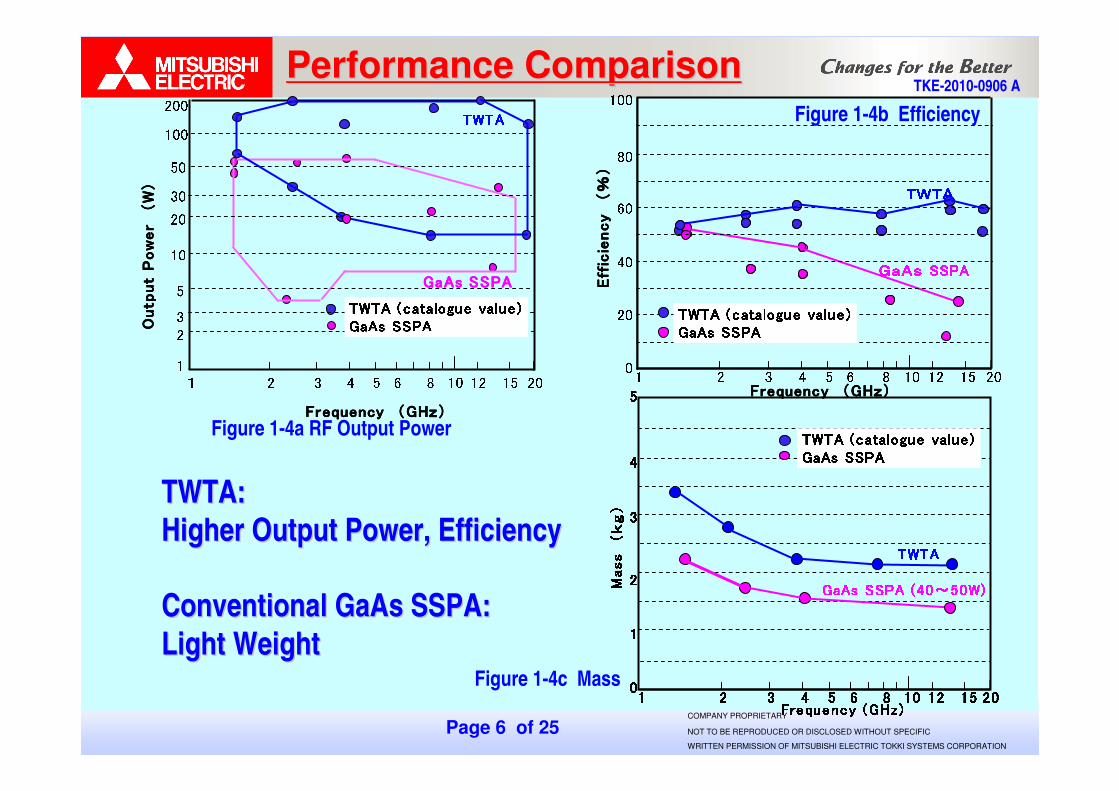
TKE-2010-0906 APerformance ComparisonPerformance Comparison
������������������������������������
� � � � ��� � � � � � � � � � � �� � � � ��� � � � � � � � � � � �� � � � ��� � � � � � � � � � � �� � � � ��� � � � � � � � � � � �� � �� � �� �� � �� � �� �� � �� � �� �� � �� � �� �
� � � � � � � �� � � � � ��
� � � � �� � � � �� � � � �� � � � � � �� �� �� � � ������� � �� �� �� �
� � � �� � � �� � � �� � � ��� ���
��
���
���� �
��
����������
����������
����������
���������� �������� �� ��
�
TWTATWTA::Higher OHigher Output Power, Efficiencyutput Power, Efficiency
CConventional GaAs SSPAonventional GaAs SSPA::Light WeightLight Weight
� � � � ! " �# � � � �##�#
�#!#
"#�# #
������������������������������������ � �� �� �� � � � � �
����������
����������
����������
������������
��
��
�� $ % $ &$ % $ &$ % $ &$ % $ &
'( &)'( &)'( &)'( &) * *+ ,* *+ ,* *+ ,* *+ ,
-. - , /�0 1 2 1 345 6 78 1 3 6 7 9-. - , /�0 1 2 1 345 6 78 1 3 6 7 9-. - , /�0 1 2 1 345 6 78 1 3 6 7 9-. - , /�0 1 2 1 345 6 78 1 3 6 7 9: 1 ,; * * + ,: 1 ,; * * + ,: 1 ,; * * + ,: 1 ,; * * + ,
<< <<== ==
>> >>?? ??
@@ @@AA AA
B CDD
B CDD
B CDD
B CDD
EFGH
EFGH
EFGH
EFGH
@@ @@ ?? ?? >> >> == == << << II II JJ JJ @ A@ A@ A@ A @ ?@ ?@ ?@ ? @ <@ <@ <@ < ? A? A? A? AKLM NO M PQ R ST UV WKLM NO M PQ R ST UV WKLM NO M PQ R ST UV WKLM NO M PQ R ST UV WXY X ZXY X ZXY X ZXY X Z
T [ Z\ ] ]^ ZT [ Z\ ] ]^ ZT [ Z\ ] ]^ ZT [ Z\ ] ]^ Z SS SS = A= A= A= A__ __ < A< A< A< A YY YY WW WW
XY X Z SQ [ ` [ abc O M d [ a O M WXY X Z SQ [ ` [ abc O M d [ a O M WXY X Z SQ [ ` [ abc O M d [ a O M WXY X Z SQ [ ` [ abc O M d [ a O M W
T [ Z\ ] ]^ ZT [ Z\ ] ]^ ZT [ Z\ ] ]^ ZT [ Z\ ] ]^ Z
Figure 1-4a RF Output Power
Figure 1-4b Efficiency
Figure 1-4c Mass

Page 7 of 25 COMPANY PROPRIETARY
NOT TO BE REPRODUCED OR DISCLOSED WITHOUT SPECIFIC
WRITTEN PERMISSION OF MITSUBISHI ELECTRIC TOKKI SYSTEMS CORPORATION
TKE-2010-0906 A
Limit of the conventional GaAs SSPALimit of the conventional GaAs SSPA
More Powerful device is desiredMore Powerful device is desired
Limit of handling power (25W max)Limit of handling power (25W max)
Multiple power combining to achieve higher Multiple power combining to achieve higher output poweroutput power
Wider footprint / Heavier massWider footprint / Heavier mass
1. High Power Amplifier1. High Power Amplifier
Page 8 of 25 COMPANY PROPRIETARY
NOT TO BE REPRODUCED OR DISCLOSED WITHOUT SPECIFIC
WRITTEN PERMISSION OF MITSUBISHI ELECTRIC TOKKI SYSTEMS CORPORATION
TKE-2010-0906 A
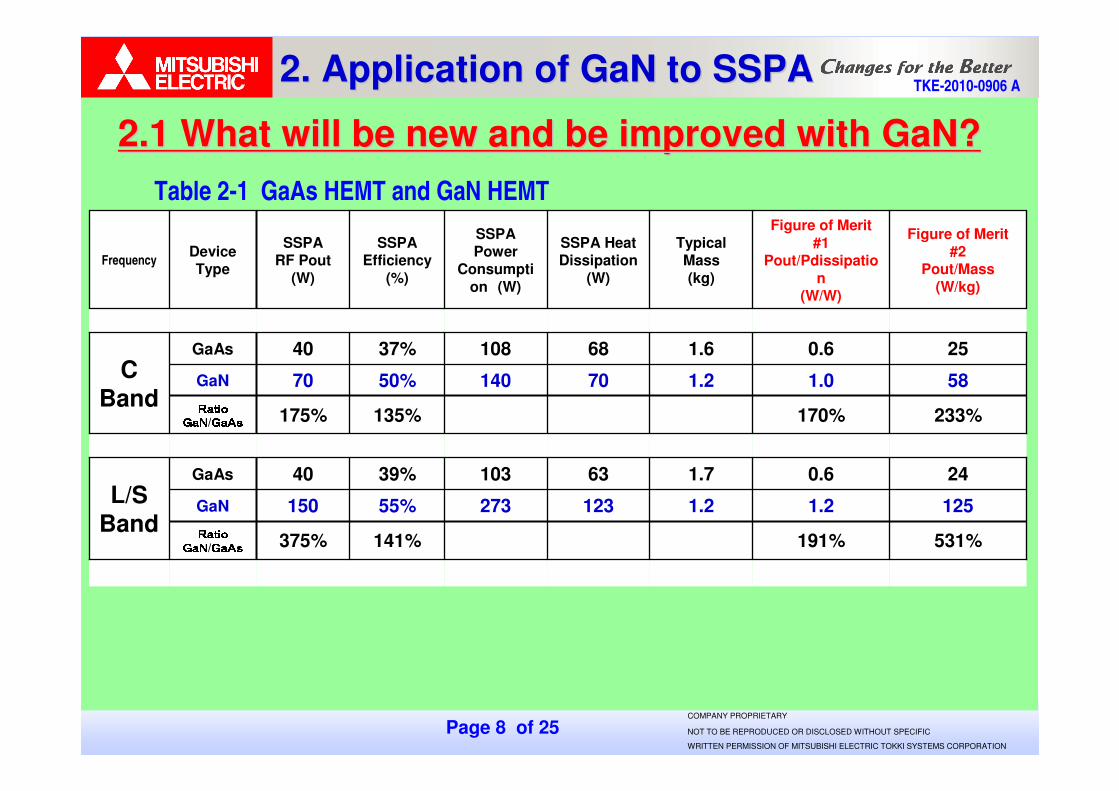
25 0.6 1.6 68 108 37%40GaAsC
Band58 1.0 1.2 70 140 50%70GaN
233%170%135%175%
ef g hief g hief g hief g hij f kj f kj f kj f k
/
j f lmj f lmj f lmj f lm
531%191%141%375%
ef g hief g hief g hief g hij f kj f kj f kj f k
/
j f lmj f lmj f lmj f lm
125 1.2 1.2 123 273 55%150GaN
24 0.6 1.7 63 103 39%40GaAsL/S
Band
Figure of Merit #2
Pout/Mass (W/kg)
Figure of Merit #1
Pout/Pdissipation
(W/W)
Typical Mass (kg)
SSPA Heat Dissipation
(W)
SSPA Power
Consumption (W)
SSPA Efficiency
(%)
SSPA RF Pout
(W)
DeviceType
Frequency
2.1 What will be new and be improved with GaN?2.1 What will be new and be improved with GaN?
2. Application of GaN to SSPA 2. Application of GaN to SSPA
Table 2-1 GaAs HEMT and GaN HEMT
Page 9 of 25 COMPANY PROPRIETARY
NOT TO BE REPRODUCED OR DISCLOSED WITHOUT SPECIFIC
WRITTEN PERMISSION OF MITSUBISHI ELECTRIC TOKKI SYSTEMS CORPORATION
TKE-2010-0906 A
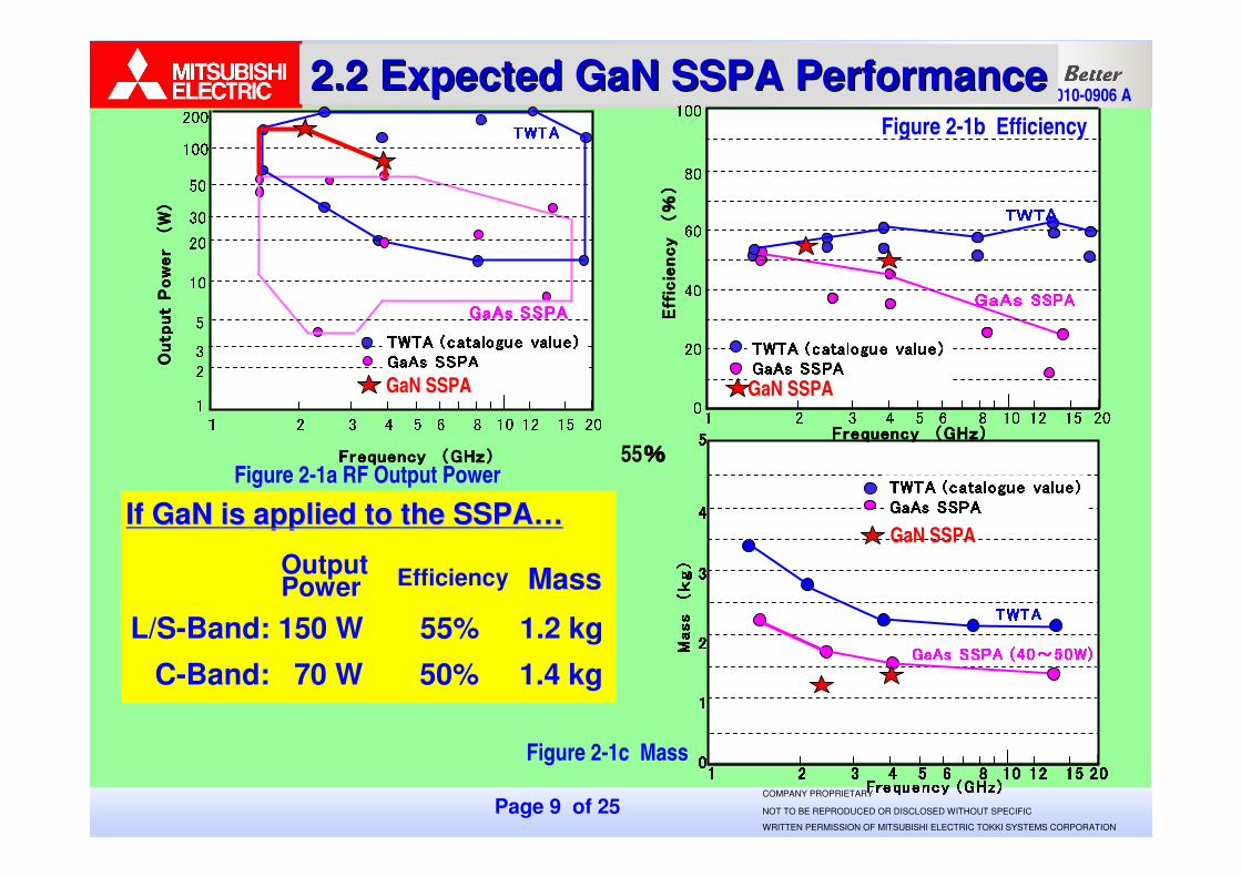
If GaN is applied to the SSPAIf GaN is applied to the SSPA……
2.2 Expected GaN SSPA Performance2.2 Expected GaN SSPA Performance
������������������������������������
� � � � ��� � � � � � � � � � � �� � � � ��� � � � � � � � � � � �� � � � ��� � � � � � � � � � � �� � � � ��� � � � � � � � � � � �� � �� � �� �� � �� � �� �� � �� � �� �� � �� � �� �
� � � � � � � �� � � � � ��
� � � � �� � � � �� � � � �� � � � � � �� �� �� � � ������� � �� �� �� �
� � � �� � � �� � � �� � � ��� ���
��
���
���� �
��
����������
����������
����������
���������� �������� �� ��
�
� � � � ! " �# � � � �##�#
�#!#
"#�# #
������������������������������������ � �� �� �� � � � � �
����������
����������
����������
������������
��
��
�� $ % $ &$ % $ &$ % $ &$ % $ &
'( &)'( &)'( &)'( &) * *+ ,* *+ ,* *+ ,* *+ ,
-. - , /�0 1 2 1 345 6 78 1 3 6 7 9-. - , /�0 1 2 1 345 6 78 1 3 6 7 9-. - , /�0 1 2 1 345 6 78 1 3 6 7 9-. - , /�0 1 2 1 345 6 78 1 3 6 7 9: 1 ,; * * + ,: 1 ,; * * + ,: 1 ,; * * + ,: 1 ,; * * + ,
<< <<== ==
>> >>?? ??
@@ @@AA AA
B CDD
B CDD
B CDD
B CDD
EFGH
EFGH
EFGH
EFGH
@@ @@ ?? ?? >> >> == == << << II II JJ JJ @ A@ A@ A@ A @ ?@ ?@ ?@ ? @ <@ <@ <@ < ? A? A? A? AKLM NO M PQ R ST UV WKLM NO M PQ R ST UV WKLM NO M PQ R ST UV WKLM NO M PQ R ST UV WXY X ZXY X ZXY X ZXY X Z
T [ Z\ ] ]^ ZT [ Z\ ] ]^ ZT [ Z\ ] ]^ ZT [ Z\ ] ]^ Z SS SS = A= A= A= A__ __ < A< A< A< A YY YY WW WW
XY X Z SQ [ ` [ abc O M d [ a O M WXY X Z SQ [ ` [ abc O M d [ a O M WXY X Z SQ [ ` [ abc O M d [ a O M WXY X Z SQ [ ` [ abc O M d [ a O M W
T [ Z\ ] ]^ ZT [ Z\ ] ]^ ZT [ Z\ ] ]^ ZT [ Z\ ] ]^ Z
GaN SSPA
GaN SSPA
GaN SSPA
L/S-Band: 150 W 55% 1.2 kgC-Band: 70 W 50% 1.4 kg
EfficiencyOutputPower Mass
55����Figure 2-1a RF Output Power
Figure 2-1b Efficiency
Figure 2-1c Mass

Page 10 of 25 COMPANY PROPRIETARY
NOT TO BE REPRODUCED OR DISCLOSED WITHOUT SPECIFIC
WRITTEN PERMISSION OF MITSUBISHI ELECTRIC TOKKI SYSTEMS CORPORATION
TKE-2010-0906 A
��������Development of GaN device for space application���� SQT:Space Qualification Test
��������Applying GaN performance to SSPA design- Thermal performance- Prevent arcing in vacuum environment
��������Radiation effect confirmation
2.3 2.3 Issues to be solvedIssues to be solved

Page 11 of 25 COMPANY PROPRIETARY
NOT TO BE REPRODUCED OR DISCLOSED WITHOUT SPECIFIC
WRITTEN PERMISSION OF MITSUBISHI ELECTRIC TOKKI SYSTEMS CORPORATION
TKE-2010-0906 A
GaN for space application was developed by Mitsubishi Electric.
PAE(%) & I��������(A)
3.1 Device Electrical Performance3.1 Device Electrical Performance3. GaN Device: Achieved Performance3. GaN Device: Achieved Performance
Input to Output Powerand Gain completion.
Figure 3-1a Figure 3-1b
30
35
40
45
50
55
20 25 30 35 40 45
Pin (dBm)
Pout
(dB
m)
5
10
15
20
25
30
Gp (
dB)
f=3.90GHz
f=4.00GHz
f=4.10GHz<--Pout
Gp -->
0
20
40
60
80
20 25 30 35 40 45
Pin (dBm)P
.A.E
. (%
)
0.0
2.0
4.0
6.0
8.0
Ids(
RF)
(A
)
f=3.90GHz
f=4.00GHz
f=4.10GHz
<-- PAE
Ids(RF) -->
At device level, RF output power of over 50 dBm (at P2dB) is achieved. Power added efficiency (PAE) exceeds 60 %.

Page 12 of 25 COMPANY PROPRIETARY
NOT TO BE REPRODUCED OR DISCLOSED WITHOUT SPECIFIC
WRITTEN PERMISSION OF MITSUBISHI ELECTRIC TOKKI SYSTEMS CORPORATION
TKE-2010-0906 A
(1) SQT Summary for GaN device
Figure 3-2 MTTF Evaluation
3.2 Device Qualification Status3.2 Device Qualification Status
Group Test Item Results
Temperature Cycling 1051 -65/+175 deg.C, 210cycles
Shock 2016 1500G, 3 axis
Vibration 2051 100-2000 Hz
Constant Acceleration 2006 10000 G
Seal Test 1071 Gross and Fine leak
Internal Visual 2075SEM 2077Bond Strength 2037Die Shear Strength 2017RF Life Test 1026 1000 hr r/n=0/2DC Life Test 1026 1000 hr r/n=0/8Li
feTe
stM
echa
nica
l Tes
t
Test Condition MIL-STD-750Method
r/n=0/11
r/n=0/3
Table 3-1 SQT Result of GaN HEMT
2 test results with Vds=47V are obtained.� Expected MTTF = 1.0x10⁶ h at Tch=175 degC
Test Result with 270 degC, Vds 45V is obtained�MTTF with Vds=45 degC :1.3x10⁶ hr at Tch=175 degC

Page 13 of 25 COMPANY PROPRIETARY
NOT TO BE REPRODUCED OR DISCLOSED WITHOUT SPECIFIC
WRITTEN PERMISSION OF MITSUBISHI ELECTRIC TOKKI SYSTEMS CORPORATION
TKE-2010-0906 A
� �� �� �� �
� �� �� �� �
� �� �� �� �
� �� �� �� �
� �� �� �� �
� �� �� �� �
� �� �� �� �
� � � � � � � � ����� �� �� �� � � � � � � � � � ����� �� �� �� � � � � � � � � � ����� � � � � � � � � � � � ����� �� �� �� � � � � � � � � � ����� � � � � � � � � � � � � � � � � � � � � � � �
� � � � � � � � � � � � � � � �� � � � � � � � � � � � � � � �� � � � � � � � � � � � � � � �� � � � � � � � � � � � � � � �
���������
���������
���������
���������
100WClass GaN HPA
Test Fixture for Arcing Test
High Vacuum
Figure 3-4 Output Power MonitorFigure 3-3 Test Set-up for Arcing Test
no p3.2 (2) Arcing Test Results
qr sSG PM
tu v
qr s
Vacuum Chamber
Signal Generator
Power Monitor
Vacuum gauge
Arcing test was performed with GaN device (100W class) . There was no arcing at all from ambient pressure to high vacuum environment.
RF output power monitor remains stable during depressurization

Page 14 of 25 COMPANY PROPRIETARY
NOT TO BE REPRODUCED OR DISCLOSED WITHOUT SPECIFIC
WRITTEN PERMISSION OF MITSUBISHI ELECTRIC TOKKI SYSTEMS CORPORATION
TKE-2010-0906 A
(1) Single Event Tests:Radiation hardness test for single event effect (SEB, SEGR)Test condition;- Ion Beam : Br+13 (145MeV) (Br: Bromine)- LET (Liner Energy Transfer): 31.2MeV/(mg/cm2)- Beam fluence : 1x10⁶ ions/cm2
3.3 Device Radiation Hardness Tests3.3 Device Radiation Hardness Tests
Figure 3-5 Radiation Test Equipment
Figure 3-6 GaN Test Fixture

Page 15 of 25 COMPANY PROPRIETARY
NOT TO BE REPRODUCED OR DISCLOSED WITHOUT SPECIFIC
WRITTEN PERMISSION OF MITSUBISHI ELECTRIC TOKKI SYSTEMS CORPORATION
TKE-2010-0906 A
The device operating condition: Vds=50V,Pout=P13dBTable3-2 RF drive condition & irradiation result
3.3 (1) Single Event
no degradation
Figure 3-7a Figure 3-7b Figure 3-7c

Page 16 of 25 COMPANY PROPRIETARY
NOT TO BE REPRODUCED OR DISCLOSED WITHOUT SPECIFIC
WRITTEN PERMISSION OF MITSUBISHI ELECTRIC TOKKI SYSTEMS CORPORATION
TKE-2010-0906 A
Cobalt-60 gamma ray was irradiated on GaN device.126kGy with RF input, bias Vds=45V,Ids=0.22A ���� No Degradation86kGy with no RF, pinch-off bias Vds=45V,Vgs=-5V ���� No Degradation
Table3-3 Bias condition & irradiation result
The Result of Irradiation test after Vd=45V, Id=0.22A operation
3.3 (2) Total Ionizing Dose
Figure 3-8a Figure 3-8b Figure 3-8c
Page 17 of 25 COMPANY PROPRIETARY
NOT TO BE REPRODUCED OR DISCLOSED WITHOUT SPECIFIC
WRITTEN PERMISSION OF MITSUBISHI ELECTRIC TOKKI SYSTEMS CORPORATION
TKE-2010-0906 A
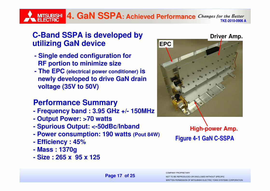
Performance Summary- Frequency band : 3.95 GHz +/- 150MHz- Output Power: >70 watts - Spurious Output: <-50dBc/Inband- Power consumption: 190 watts (Pout 84W)- Efficiency : 45%- Mass : 1370g- Size : 265 x 95 x 125
Driver Amp.
High-power Amp.
EPC
4. GaN SSPA4. GaN SSPA: Achieved Performance: Achieved Performance
C-Band SSPA is developed by utilizing GaN device- Single ended configuration forRF portion to minimize size
- The EPC (electrical power conditioner) isnewly developed to drive GaN drainvoltage (35V to 50V)
Figure 4-1 GaN C-SSPA

Page 18 of 25 COMPANY PROPRIETARY
NOT TO BE REPRODUCED OR DISCLOSED WITHOUT SPECIFIC
WRITTEN PERMISSION OF MITSUBISHI ELECTRIC TOKKI SYSTEMS CORPORATION
TKE-2010-0906 A
Frequency vs. Output Power characteristics Frequency vs. Output Power characteristics
The output power achieved 70W
Figure 4-3 Liner Gain
Figure 4-2 Output Power versus Frequency Characteristics
60
70
80
90
100
110
3 3.5 4 4.5 5Frequency [GHz]
Gai
n [d
B]
Linear Gain achieved 100dB
4. GaN SSPA4. GaN SSPA: Achieved Performance: Achieved Performance
30
35
40
45
50
55
3.7 3.8 3.9 4 4.1 4.2
Frequency [GHz]
Out
put P
ower
[dB
m]
Target line:70W

Page 19 of 25 COMPANY PROPRIETARY
NOT TO BE REPRODUCED OR DISCLOSED WITHOUT SPECIFIC
WRITTEN PERMISSION OF MITSUBISHI ELECTRIC TOKKI SYSTEMS CORPORATION
TKE-2010-0906 A
Figure 4-4 Output Power & Efficiency at CW
CW characteristicsCW characteristics
4. GaN SSPA4. GaN SSPA: Achieved Performance: Achieved Performance
30.00
35.00
40.00
45.00
50.00
-25.00 -20.00 -15.00 -10.00 -5.00 0.00 5.00
Relative Input Power [dB]
Out
put P
ower
[dB
m]
0.00
20.00
40.00
60.00
80.00
Pow
er A
dded
Effi
cien
cy [%
]
-10deg.C+25deg.C+60deg.C
Pout>85WPAE>45% at P2dB
Normalized with 2dB output power compression point (P2dB)
45.93dBm=85W Output Power
Power Added Efficiency
45
w
min.

Page 20 of 25 COMPANY PROPRIETARY
NOT TO BE REPRODUCED OR DISCLOSED WITHOUT SPECIFIC
WRITTEN PERMISSION OF MITSUBISHI ELECTRIC TOKKI SYSTEMS CORPORATION
TKE-2010-0906 A
Out put Power at Multi carriers
Figure 4-6 NPR:Noise Power Ratio
30
35
40
45
50
55
-15 -10 -5 0 5
Relative Input Power [dB]
Out
put P
ower
[dB
m]
MultiMulti--carrier characteristicscarrier characteristics
Multi carrier BW=80MHzTone value:80001
4. GaN SSPA4. GaN SSPA: Achieved Performance: Achieved Performance
xy
z xz y
{ x{ y
| x| y
} x~ z x ~ y x y
�� �� � �� � �� �� � � ��� �� ��� �
��� �
�� �
Noise BW=80MHz
Tone value:80001
Figure 4-5 Input to Output Power with Multi-Carrier
Page 21 of 25 COMPANY PROPRIETARY
NOT TO BE REPRODUCED OR DISCLOSED WITHOUT SPECIFIC
WRITTEN PERMISSION OF MITSUBISHI ELECTRIC TOKKI SYSTEMS CORPORATION
TKE-2010-0906 A
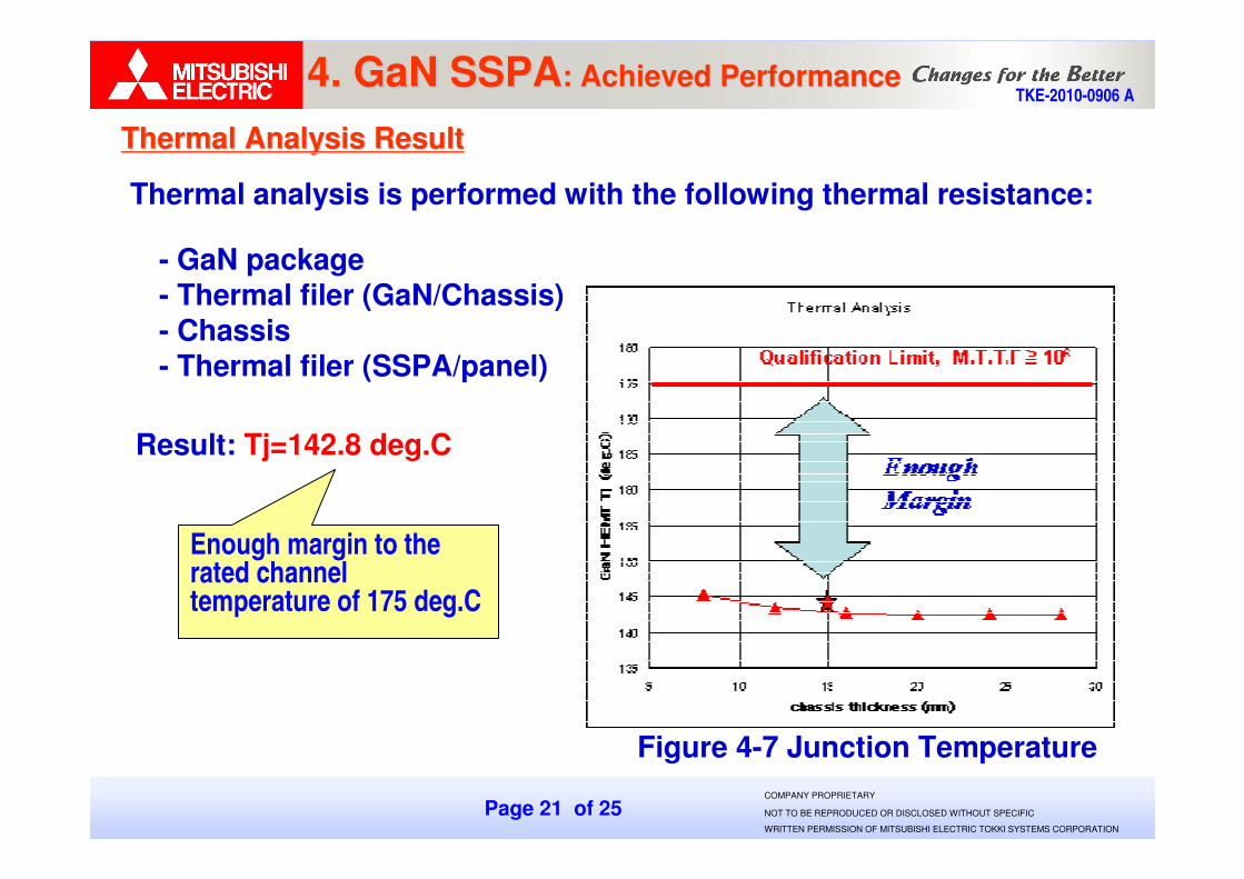
Thermal Analysis ResultThermal Analysis Result
4. GaN SSPA4. GaN SSPA: Achieved Performance: Achieved Performance
Enough margin to the rated channel temperature of 175 deg.C
Thermal analysis is performed with the following thermal resistance:
- GaN package- Thermal filer (GaN/Chassis)- Chassis- Thermal filer (SSPA/panel)
Result: Tj=142.8 deg.C
Figure 4-7 Junction Temperature

Page 22 of 25 COMPANY PROPRIETARY
NOT TO BE REPRODUCED OR DISCLOSED WITHOUT SPECIFIC
WRITTEN PERMISSION OF MITSUBISHI ELECTRIC TOKKI SYSTEMS CORPORATION
TKE-2010-0906 A4. GaN SSPA4. GaN SSPA: Achieved Performance: Achieved Performance
Qualification TestsQualification Tests
1. Thermal Vacuum Test:- Temperature : -10 deg.C to +60 deg.C- Vacuum condition :1x10⁻⁶ Torr- Test Cycle : 33 cycle
2. Vibration Test : Pass3. Mechanical Shock Test : Pass4. Electro Magnetic Compatibility : MIL-STD 462 applied
Level Remarks
Sine 20G all 3axis
14.1 Grms X, Y axis
19.7 Grms Z axis
1000G all 3axis
Item
Shock
RandomVibration
Table 4-1 Vibration & Shock Test condition
Qualification test was performed successfully based on the following test items and test conditions

Page 23 of 25 COMPANY PROPRIETARY
NOT TO BE REPRODUCED OR DISCLOSED WITHOUT SPECIFIC
WRITTEN PERMISSION OF MITSUBISHI ELECTRIC TOKKI SYSTEMS CORPORATION
TKE-2010-0906 A5. Conclusion and Next Target 5. Conclusion and Next Target
GaN SSPA was developed and achieve the following performance.
GaN device- 100 Watts class GaN is developed- Space Qualification Test is successfully completed- No arcing from ambient pressure to high vacuum environment. - Radiation Hardness is confirmed
- No SEB, No SEGR with Vd 50V, P13dB condition- No TID degradation with operation condition (Vd 45V, Id 0.22A)
SSPA Performance- 85 Watts RF output power with 45% efficiency is achieved- Single stage configuration, without power combining���� Slim and light weight is accomplished
- Qualification test is successfully completed
5.1 Achieved Results5.1 Achieved Results

Page 24 of 25 COMPANY PROPRIETARY
NOT TO BE REPRODUCED OR DISCLOSED WITHOUT SPECIFIC
WRITTEN PERMISSION OF MITSUBISHI ELECTRIC TOKKI SYSTEMS CORPORATION
TKE-2010-0906 A
30
35
40
45
50
55
3.7 3.8 3.9 4 4.1 4.2
Frequency [GHz]
Pow
er A
dded
Eff
icie
ncy
[%]
QT result
EPC efficiency:87%
Final Stage GaN efficiency:60%
Total efficiency:45%
For Next Model
EPC efficiency:94%
Final Stage GaN efficiency:65%
Total efficiency up to 50%
The total efficiency at normal temperature is 45����.
����EPC have already realized efficiency 94% in other development.
����The efficiency in finale stage GaN will be achieved 65% by the improvement of device characteristics improvement.
Power added efficiency will be improved
5.2 Target to Be Improved5.2 Target to Be Improved
Figure 5-1 Efficiency Improvement

Page 25 of 25 COMPANY PROPRIETARY
NOT TO BE REPRODUCED OR DISCLOSED WITHOUT SPECIFIC
WRITTEN PERMISSION OF MITSUBISHI ELECTRIC TOKKI SYSTEMS CORPORATION
TKE-2010-0906 A5. Conclusion and Next Target5. Conclusion and Next Target
Next Target
- Actual operation in the orbit
- Development for higher frequency operation…depends on the manufacturer

Page 26 of 25 COMPANY PROPRIETARY
NOT TO BE REPRODUCED OR DISCLOSED WITHOUT SPECIFIC
WRITTEN PERMISSION OF MITSUBISHI ELECTRIC TOKKI SYSTEMS CORPORATION
TKE-2010-0906 A
End of PresentationEnd of Presentation