Development of an Improved RF Band-Pass Filter using CSRR ...
71
Development of an Improved RF Band-Pass Filter using CSRR Metamaterial Structures on an LCP Substrate by Christopher Brent James A thesis submitted to the Graduate Faculty of Auburn University in partial fulfillment of the requirements for the Degree of Master of Science in Electrical Engineering Auburn, Alabama May 10, 2015 Keywords: Metamaterial, CSRR, Band-Pass, Filter, HFSS, LCP Approved by Robert Dean, Chair, Associate Professor of Electrical and Computer Engineering Lloyd S. Riggs, Professor of Electrical and Computer Engineering Michael Baginski, Associate Professor of Electrical and Computer Engineering
Transcript of Development of an Improved RF Band-Pass Filter using CSRR ...
Development of an Improved RF Band-Pass Filter using CSRR Metamaterial Structures on an LCP Substrate
by
Christopher Brent James
A thesis submitted to the Graduate Faculty of Auburn University
in partial fulfillment of the requirements for the Degree of
Master of Science in Electrical Engineering
Auburn, Alabama May 10, 2015
Keywords: Metamaterial, CSRR, Band-Pass, Filter, HFSS, LCP
Approved by
Robert Dean, Chair, Associate Professor of Electrical and Computer Engineering Lloyd S. Riggs, Professor of Electrical and Computer Engineering
Michael Baginski, Associate Professor of Electrical and Computer Engineering
ii
Abstract
For over a decade, academic exploration into the emerging field of metamaterial
technology has resulted in advancements in the design of myriad devices such as oscillators,
antennas, transmission lines, superlenses, and filters. Unusual electromagnetic properties unique
to metamaterial structures have also inspired new work in fields like cloaking technology and
nanotechnology. Two such structures that are of interest to RF and microwave engineering
applications are the split-ring resonator (SRR) and its dual, the complementary split-ring resonator
(CSRR). An RF band-pass filter based on a previous work is designed using a microstrip
transmission line on a substrate made of Liquid Crystal Polymer (LCP), a flexible material with
desirable RF properties such as a low dielectric constant ε. This transmission line is made of copper
and is coupled to a CSRR structure etched into a ground plane below the substrate. The band-pass
frequency response is dependent on the physical dimensions of both the microstrip line and the
CSRR structure. The proposed filter is designed as a unit cell with a single CSRR structure, and
the S-parameters of the filter are simulated for frequencies ranging from 1 GHz to 10 GHz. Both
the design and the simulation of the filter are done using HFSS, a commercial simulation tool by
ANSYS that uses finite element method (FEM) techniques to solve electromagnetic structures.
With an emphasis on improving the upper-band performance, this work seeks to design a compact
RF band-pass filter using metamaterial technology that can be applied to non-planar surfaces.
iii
Acknowledgments
The author would like to take this opportunity to recognize those who, through financial,
intellectual, or emotional means, provided the necessary support to make this work possible: the
American Society for Engineering Education and the SMART program for tuition and stipend
support; his advisor Dr. Robert Dean, as well as committee members Dr. Lloyd Riggs and Dr.
Michael Baginski, for their knowledge, patience, and professional example; Dr. Stu Wentworth,
Dr. John Hung, Dr. Shumin Wang, and others in the Auburn University Department of Electrical
and Computer Engineering for their willingness provide technical guidance and constructive
criticism; Dr. Guy Beckwith, Mr. Chris Henderson, and Ms. Vickie Lundy for their inspiration
and academic influence on his education and career decisions; Udarius Blair, Byron Caudle,
William Little, and Christopher Wilson for their academic and technical advice; his parents,
Brent and Beth James, as well as the rest of his family and friends for their consistent and
unwavering support; and his wife, Alison, for always believing.

iv
TableofContents
Abstract ........................................................................................................................................... ii
Acknowledgments.......................................................................................................................... iii
Table of Figures .............................................................................................................................. v
List of Abbreviations ................................................................................................................... viii
Chapter 1: Introduction ................................................................................................................... 1
Chapter 2: Metamaterial Theory ..................................................................................................... 4
Chapter 3: Microwave Filter Theory ............................................................................................ 15
Chapter 4: Metamaterial Filters .................................................................................................... 26
Chapter 5: HFSS ........................................................................................................................... 37
Chapter 6: Improved BPF Design ................................................................................................. 50
Chapter 7: Conclusion................................................................................................................... 59
Chapter 8: Future Work ................................................................................................................ 60
Bibliography ................................................................................................................................. 61

v
TableofFigures
Figure 2-1 ........................................................................................................................................ 6
Figure 2-2 ........................................................................................................................................ 6
Figure 2-3 ........................................................................................................................................ 7
Figure 2-4 ........................................................................................................................................ 8
Figure 2-5 ........................................................................................................................................ 9
Figure 2-6 ...................................................................................................................................... 10
Figure 2-7 ...................................................................................................................................... 11
Figure 2-8 ...................................................................................................................................... 12
Figure 2-9 ...................................................................................................................................... 13
Figure 2-10 .................................................................................................................................... 13
Figure 3-1 ...................................................................................................................................... 16
Figure 3-2 ...................................................................................................................................... 17
Figure 3-3 ...................................................................................................................................... 18
Figure 3-4 ...................................................................................................................................... 19
Figure 3-5 ...................................................................................................................................... 20
Figure 3-6 ...................................................................................................................................... 21
Figure 3-7 ...................................................................................................................................... 21
Figure 3-8 ...................................................................................................................................... 23
Figure 3-9 ...................................................................................................................................... 25
Figure 4-1 ...................................................................................................................................... 27
Figure 4-2 ...................................................................................................................................... 28
Figure 4-3 ...................................................................................................................................... 29
vi
Figure 4-4 ...................................................................................................................................... 30
Figure 4-5 ...................................................................................................................................... 31
Figure 4-6 ...................................................................................................................................... 32
Figure 4-7 ...................................................................................................................................... 33
Figure 4-8 ...................................................................................................................................... 34
Figure 4-9 ...................................................................................................................................... 34
Figure 4-10 .................................................................................................................................... 35
Figure 4-11 .................................................................................................................................... 35
Figure 4-12 .................................................................................................................................... 36
Figure 5-1 ...................................................................................................................................... 38
Figure 5-2 ...................................................................................................................................... 39
Figure 5-3 ...................................................................................................................................... 40
Figure 5-4 ...................................................................................................................................... 41
Figure 5-5 ...................................................................................................................................... 41
Figure 5-6 ...................................................................................................................................... 42
Figure 5-7 ...................................................................................................................................... 43
Figure 5-8 ...................................................................................................................................... 43
Figure 5-9 ...................................................................................................................................... 44
Figure 5-10 .................................................................................................................................... 45
Figure 5-11 .................................................................................................................................... 45
Figure 5-12 .................................................................................................................................... 46
Figure 5-13 .................................................................................................................................... 47
Figure 5-14 .................................................................................................................................... 48

vii
Figure 5-15 .................................................................................................................................... 49
Figure 6-1 ...................................................................................................................................... 50
Figure 6-2 ...................................................................................................................................... 51
Figure 6-3 ...................................................................................................................................... 52
Figure 6-4 ...................................................................................................................................... 53
Figure 6-5 ...................................................................................................................................... 54
Figure 6-6 ...................................................................................................................................... 55
Figure 6-7 ...................................................................................................................................... 56
Figure 6-8 ...................................................................................................................................... 56
Figure 6-9 ...................................................................................................................................... 57
Figure 6-10 .................................................................................................................................... 58

viii
ListofAbbreviations
RF Radio frequency
LHM Left-handed medium
DNG Double-negative
LCP Liquid crystal polymer
SRR Split-ring resonator
CSRR Complementary split-ring resonator
CPW Coplanar waveguide
CRLH Composite right/left-handed
MEMS Microelectromechanical systems
SAW Surface acoustic wave
BAW Bulk acoustic wave
LPF Low-pass filter
HPF High-pass filter
BSF Band-stop filter
BPF Band-pass filter
FEM Finite element method

1
Chapter1 Introduction
Influenced by the theoretical foundation established by Veselago in 1967, the works of
Smith and Pendry near the beginning of the 21st century made possible the science of metamaterials
[1] [2] [3]. These man-made structures, capable of unusual electromagnetic behavior not found in
nature, have made possible novel approaches to the design of well-known electronic devices such
as antennas, oscillators, lenses, and filters [4] [5] [6] [7]. Additionally, the advancement of
metamaterial theory has opened doors for research in fields such as superlenses and cloaking
technology.
Contrary to the name, metamaterials are actually not conventional materials, in the sense
that they are not novel or synthetic substances. Rather, a metamaterial object is generally
composed of periodic arrays of small artificial structures called unit cells made from dielectric
materials, plastics, metals, and other commonly-used materials that have been engineered into
specific structures or shapes. The properties and arrangement of these unit cells are what give the
metamaterial its unique traits. In this sense, a metamaterial device can be considered analogous to
matter, where its inherent properties are determined by the combination of smaller “building
blocks” of different elements. In the case of matter, these properties are determined by the amount
and arrangement of the atoms in the material and the types of bonds that exist between them; in
the case of a metamaterial, its properties are determined by the physical dimensions of the unit
cells that compose the device as well as the electromagnetic coupling mechanisms that enable its
operation.
Since the early 2000s, the most common topic in metamaterials research is the concept of
negative index metamaterials, also known as left-handed media (LHM) or double negative (DNG)
2
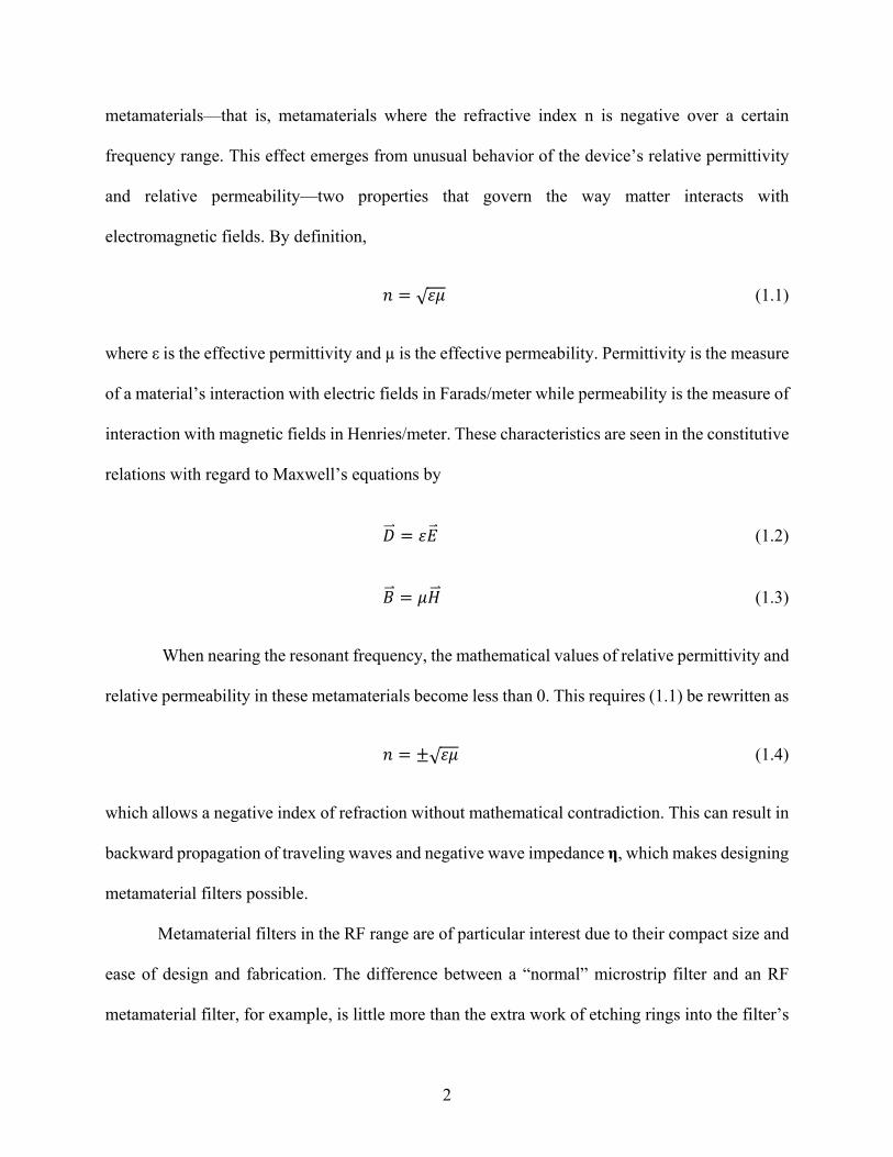
metamaterials—that is, metamaterials where the refractive index n is negative over a certain
frequency range. This effect emerges from unusual behavior of the device’s relative permittivity
and relative permeability—two properties that govern the way matter interacts with
electromagnetic fields. By definition,
√ (1.1)
where ε is the effective permittivity and µ is the effective permeability. Permittivity is the measure
of a material’s interaction with electric fields in Farads/meter while permeability is the measure of
interaction with magnetic fields in Henries/meter. These characteristics are seen in the constitutive
relations with regard to Maxwell’s equations by
(1.2)
(1.3)
When nearing the resonant frequency, the mathematical values of relative permittivity and
relative permeability in these metamaterials become less than 0. This requires (1.1) be rewritten as
√ (1.4)
which allows a negative index of refraction without mathematical contradiction. This can result in
backward propagation of traveling waves and negative wave impedance η, which makes designing
metamaterial filters possible.
Metamaterial filters in the RF range are of particular interest due to their compact size and
ease of design and fabrication. The difference between a “normal” microstrip filter and an RF
metamaterial filter, for example, is little more than the extra work of etching rings into the filter’s

3
ground plane. Since metamaterials devices are composed of unit cells, high order filters can easily
be fabricated using simple periodic arrangements of these structures. Also, since the frequency
response is dependent upon the physical dimensions of the device and its components, factors like
center frequency and bandwidth can be easily tuned by simply modifying the length, width, and
height of the signal line and the metamaterial shapes. In the case of metamaterial filters, the filter
type (low-pass, high-pass, band-pass, band-stop) can also be changed by adding or removing
etched gaps and shunt stubs in the signal line.
The applications of negative-index metamaterials range from novel circuits for RF
communication to potentially RF cloaking devices and everything in between. Even though the
field of metamaterial technology has only recently become a practical reality, the interest and work
in the field so far show the possibilities of continued exploration into novel designs of these
devices.
4
Chapter2 Metamaterial Theory
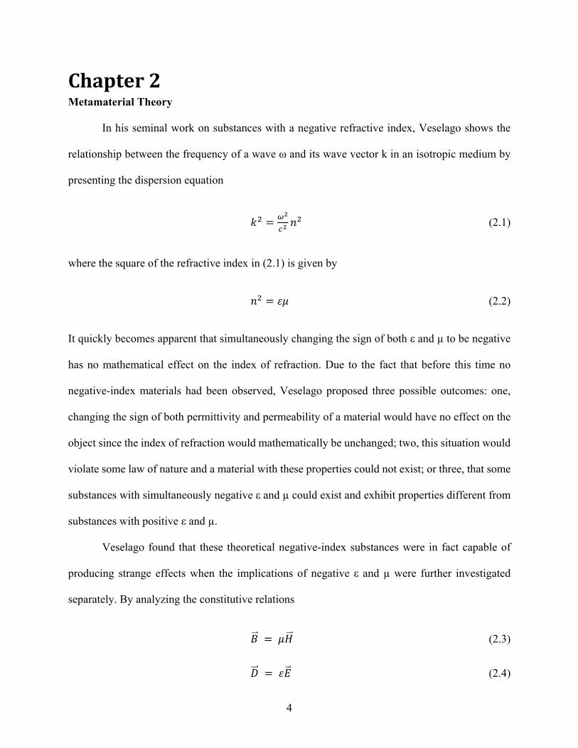
In his seminal work on substances with a negative refractive index, Veselago shows the
relationship between the frequency of a wave ω and its wave vector k in an isotropic medium by
presenting the dispersion equation
(2.1)
where the square of the refractive index in (2.1) is given by
(2.2)
It quickly becomes apparent that simultaneously changing the sign of both ε and µ to be negative
has no mathematical effect on the index of refraction. Due to the fact that before this time no
negative-index materials had been observed, Veselago proposed three possible outcomes: one,
changing the sign of both permittivity and permeability of a material would have no effect on the
object since the index of refraction would mathematically be unchanged; two, this situation would
violate some law of nature and a material with these properties could not exist; or three, that some
substances with simultaneously negative ε and µ could exist and exhibit properties different from
substances with positive ε and µ.
Veselago found that these theoretical negative-index substances were in fact capable of
producing strange effects when the implications of negative ε and µ were further investigated
separately. By analyzing the constitutive relations
(2.3)
(2.4)

5
Veselgo found that, under the condition of 0 and 0, , , and k form a “left-handed” set
of vectors where the directions of the Poynting vector and the wave vector k are in opposite
directions. This leads to a material with negative group velocity which Veselago named a “left-
handed substance.” Effects that follow from this property include a reversal of the Doppler effect,
where an increase or decrease in frequency at the receiver will be the opposite of what it would be
in the usual “right-handed” case.
Another interesting phenomenon arises when the boundary conditions between two media
are considered. To satisfy the tangential and normal components of the and fields at the
boundary, the following equations must hold true:
(2.5)
(2.6)
It can be seen, then, that the signs of the normal components of and can be negative under the
appropriate circumstances, leading to a change in the direction of the normal component of the
field. Considering Snell’s Law
√
√ (2.7)
leads to a situation where a ray traveling from a right-handed medium to a left-handed medium
can experience unusual refraction behavior as shown in Figure 2-1. Note that the ray is refracted
at a negative angle with respect to the normal and that its direction of propagation is back to the
inside of the shaded region. This unusual trajectory would be reexamined later as part of the first
modern realization of negative-index materials.

6
Figure 2-1: Wave refraction of an incident wave in the double-
negative case (left) and a normal case. [8]
Near the turn of the century, Veselgo’s hypothesis of negative-index materials was realized
in the work of John Pendry [3]. Pendry proposed a “super lens,” a device that would be matched
to free space by the reversal of the phase shift of light as it moves away from a source, effectively
having perfect focus. An illustration of light traveling through the theoretical lens is given below
in Figure 2-2.
Figure 2-2: The path of a ray through a negative-index material is shown. The ray is
bent at a negative angle which forces it to converge back to a point. [9]
Note that the ray in the figure enters the slab and then bends at a negative angle back towards the
normal then bends back to a point upon exiting the slab. By tuning this material correctly, a perfect
7
match can be made between free space and the slab, resulting in what Pendry called a “perfect
lens.”
This device would require a negative index of refraction, and therefore negative values of
permeability and permittivity according to Equation 2.2. Previous work by Pendry and others had
already established that periodic arrays of small sub-wavelength structures could yield negative
permeability or permittivity, but an element showing simultaneously negative parameters—a true
negative-index material—had not yet been presented [9] [10]. Pendry showed that infinitely long
wires in a cube lattice structure could result in a negative εeff, and later he followed this work by
demonstrating negative µeff through thin sheets of metal cut into split ring shapes in a three-
dimensional array.
Smith and others at UCSD combined the two by experimentally demonstrating negative-
index behavior capable of backwards wave propagation using conducting split-ring resonators
(SRRs) in what were named “metamaterials.” [11] By spacing these conducting elements at a
distance much less than a wavelength apart in periodic arrays, a medium was created that had both
negative permittivity and negative permeability and therefore a negative index of refraction. An
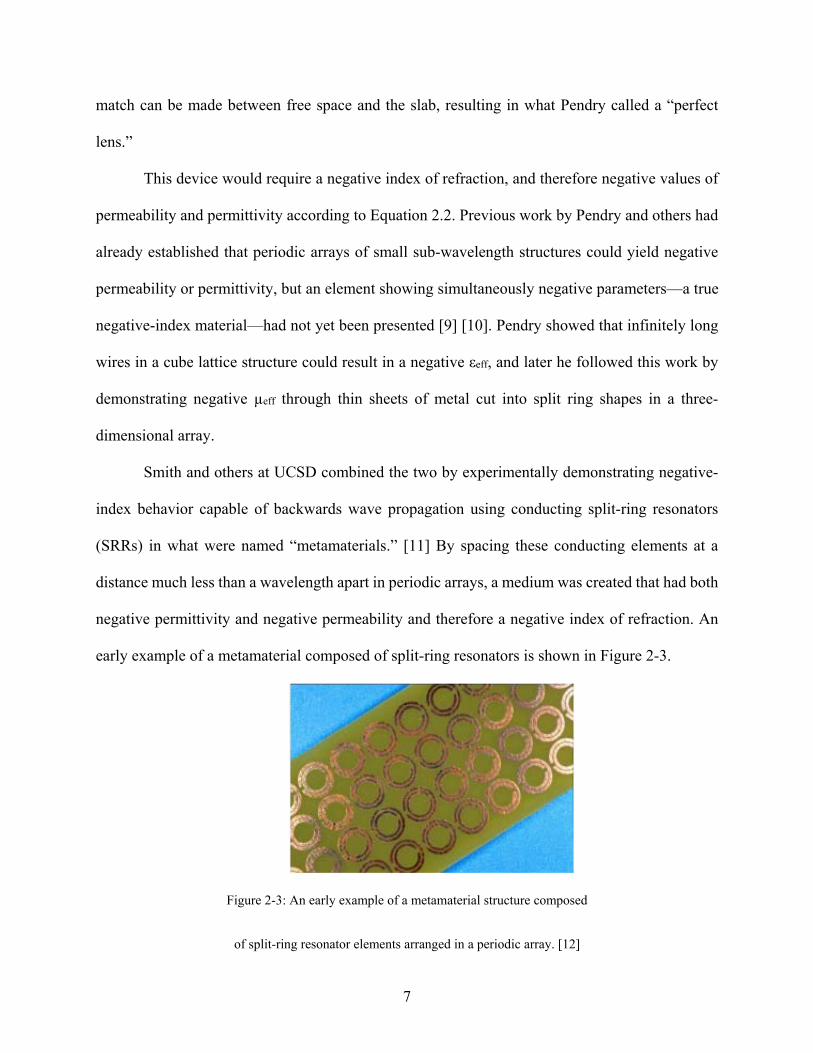
early example of a metamaterial composed of split-ring resonators is shown in Figure 2-3.
Figure 2-3: An early example of a metamaterial structure composed
of split-ring resonator elements arranged in a periodic array. [12]

8
Using this structure, the analogy of a metamaterial to a conventional material can be made.
While the properties of conventional materials are dictated by chemical composition (the
arrangement of individual atoms and molecules and the properties associated with their chemical
bonds), metamaterial properties are derived from periodic elements ranging in size from
nanometers to millimeters (and therefore made up of several atoms) that compose the larger
structure. That is, each SRR in the metamaterial acts as a single atom as shown below in Figure 2-
4.
Figure 2-4: Split-ring resonator structures in metamaterials are like atoms in conventional materials,
acting as small “building blocks” and giving the larger structure its unique properties. [12]
The SRR is a relatively simple structure made of two concentric metal rings, each with a
gap on opposing sides of the element. One ring sits inside of another with a set separation distance
between the outer radius of the smaller ring and the inner radius of the larger ring. This element is
usually much smaller than a wavelength in size, and a metamaterial device can have as many as
hundreds of these elements placed at small periodic intervals. The physical dimensions of the rings
and gaps in the SRR are relevant to the properties of the resonator, and any changes in ring width,
gap width, ring spacing, or ring diameter all will affect the frequency response in some significant
9
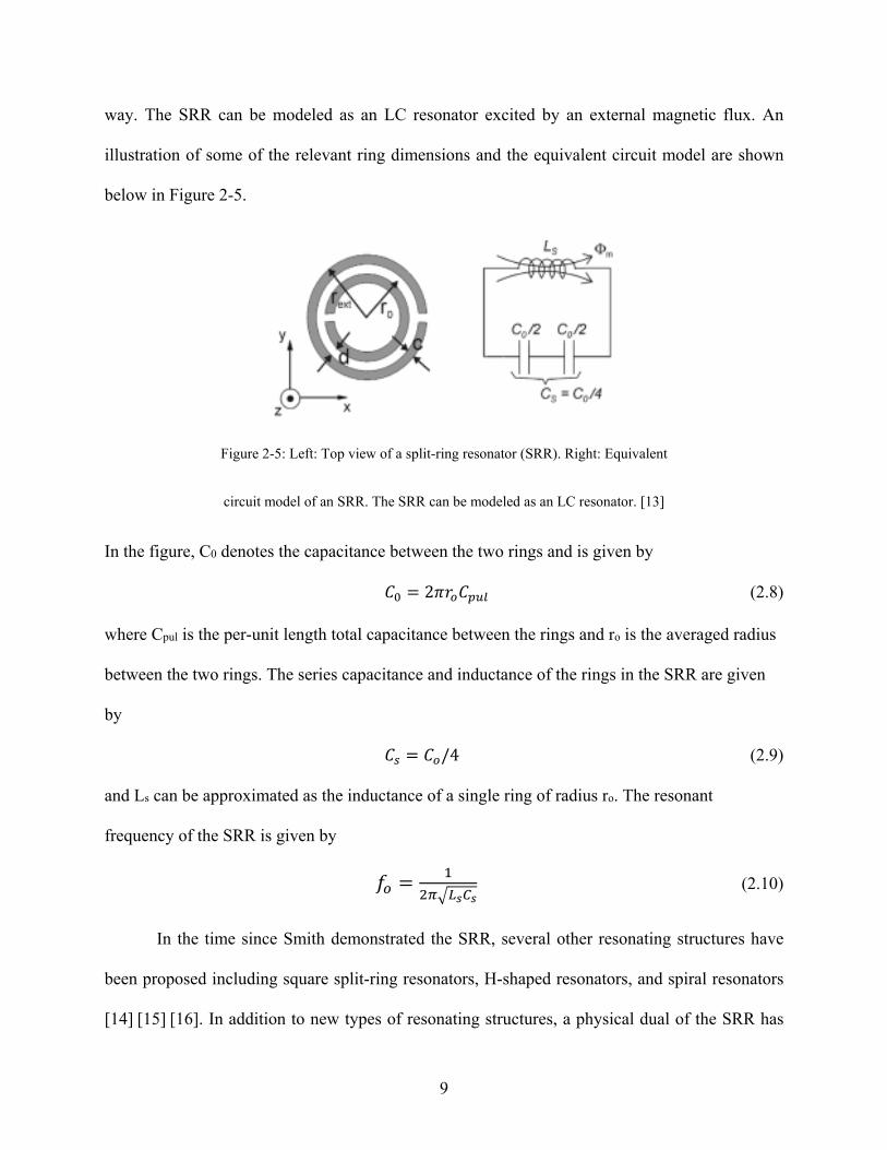
way. The SRR can be modeled as an LC resonator excited by an external magnetic flux. An
illustration of some of the relevant ring dimensions and the equivalent circuit model are shown
below in Figure 2-5.
Figure 2-5: Left: Top view of a split-ring resonator (SRR). Right: Equivalent
circuit model of an SRR. The SRR can be modeled as an LC resonator. [13]
In the figure, C0 denotes the capacitance between the two rings and is given by
2 (2.8)
where Cpul is the per-unit length total capacitance between the rings and ro is the averaged radius
between the two rings. The series capacitance and inductance of the rings in the SRR are given
by
/4 (2.9)
and Ls can be approximated as the inductance of a single ring of radius ro. The resonant
frequency of the SRR is given by
(2.10)
In the time since Smith demonstrated the SRR, several other resonating structures have
been proposed including square split-ring resonators, H-shaped resonators, and spiral resonators
[14] [15] [16]. In addition to new types of resonating structures, a physical dual of the SRR has

10
been demonstrated, called the complementary split-ring resonator (CSRR) [17]. Whereas the SRR
is usually made of some metal on top of (or etched into the top of) some substrate and incorporated
into the signal line, the CSRR is instead a negative image of the SRR and is etched into the metal
ground plane underneath the substrate and signal line. The SRR is excited by an external axial
magnetic flux while the CSRR is excited by an axial electric field. Just as above, the CSRR can be
modeled as an LC resonator following the principle of duality by replacing the shunt inductance
with series capacitance and the series capacitors with shunt inductors as shown in Figure 2-6
below.
Figure 2-6: Left: Top view of a complementary split-ring resonator (CSRR).
Right: Equivalent circuit model of a CSRR. [13]
where the parameters of the equivalent circuit model are found similar to above. L0 is given by
2 (2.8)
where Lpul is the per-unit length inductance. The series capacitance and inductance of the rings in
the CSRR are given by
/4 (2.9)
and Cc is the capacitance of a disk of radius /2. The resonant frequency of the CSRR is
given by
(2.10)
11
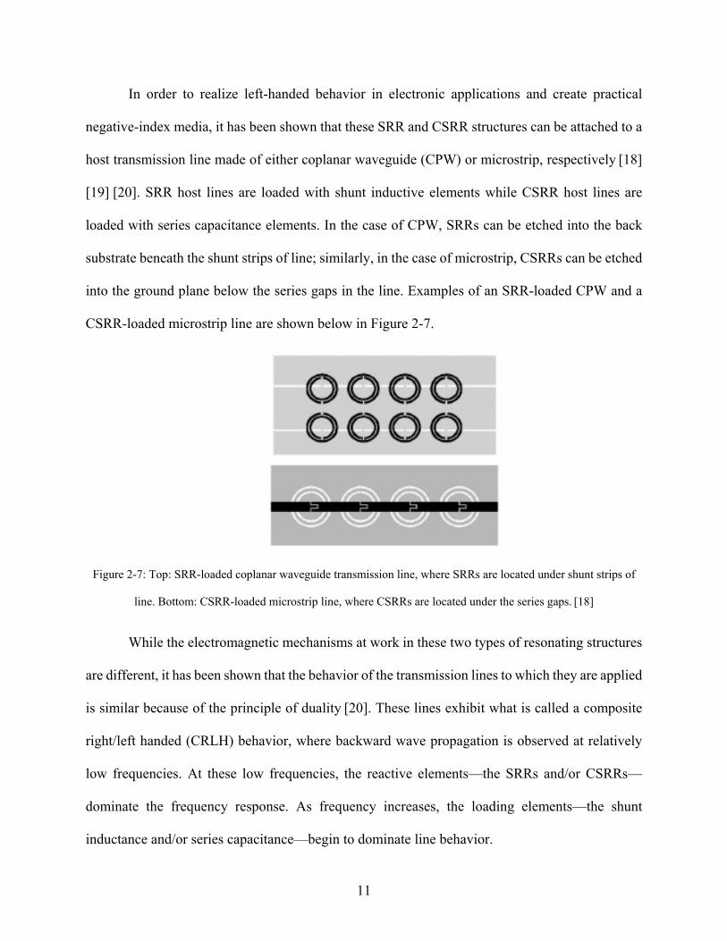
In order to realize left-handed behavior in electronic applications and create practical
negative-index media, it has been shown that these SRR and CSRR structures can be attached to a
host transmission line made of either coplanar waveguide (CPW) or microstrip, respectively [18]
[19] [20]. SRR host lines are loaded with shunt inductive elements while CSRR host lines are
loaded with series capacitance elements. In the case of CPW, SRRs can be etched into the back
substrate beneath the shunt strips of line; similarly, in the case of microstrip, CSRRs can be etched
into the ground plane below the series gaps in the line. Examples of an SRR-loaded CPW and a
CSRR-loaded microstrip line are shown below in Figure 2-7.
Figure 2-7: Top: SRR-loaded coplanar waveguide transmission line, where SRRs are located under shunt strips of
line. Bottom: CSRR-loaded microstrip line, where CSRRs are located under the series gaps. [18]
While the electromagnetic mechanisms at work in these two types of resonating structures
are different, it has been shown that the behavior of the transmission lines to which they are applied
is similar because of the principle of duality [20]. These lines exhibit what is called a composite
right/left handed (CRLH) behavior, where backward wave propagation is observed at relatively
low frequencies. At these low frequencies, the reactive elements—the SRRs and/or CSRRs—
dominate the frequency response. As frequency increases, the loading elements—the shunt
inductance and/or series capacitance—begin to dominate line behavior.
12
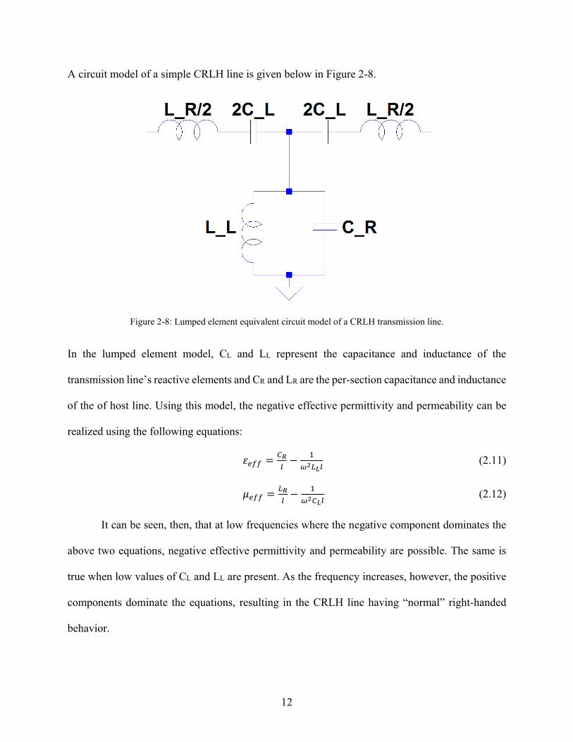
A circuit model of a simple CRLH line is given below in Figure 2-8.
Figure 2-8: Lumped element equivalent circuit model of a CRLH transmission line.
In the lumped element model, CL and LL represent the capacitance and inductance of the
transmission line’s reactive elements and CR and LR are the per-section capacitance and inductance
of the of host line. Using this model, the negative effective permittivity and permeability can be
realized using the following equations:
(2.11)
(2.12)
It can be seen, then, that at low frequencies where the negative component dominates the
above two equations, negative effective permittivity and permeability are possible. The same is
true when low values of CL and LL are present. As the frequency increases, however, the positive
components dominate the equations, resulting in the CRLH line having “normal” right-handed
behavior.
13
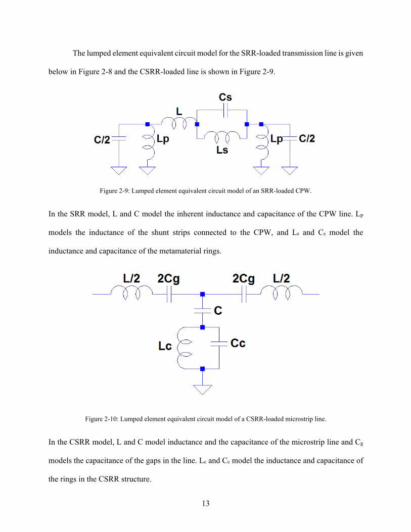
The lumped element equivalent circuit model for the SRR-loaded transmission line is given
below in Figure 2-8 and the CSRR-loaded line is shown in Figure 2-9.
Figure 2-9: Lumped element equivalent circuit model of an SRR-loaded CPW.
In the SRR model, L and C model the inherent inductance and capacitance of the CPW line. Lp
models the inductance of the shunt strips connected to the CPW, and Ls and Cs model the
inductance and capacitance of the metamaterial rings.
Figure 2-10: Lumped element equivalent circuit model of a CSRR-loaded microstrip line.
In the CSRR model, L and C model inductance and the capacitance of the microstrip line and Cg
models the capacitance of the gaps in the line. Lc and Cc model the inductance and capacitance of
the rings in the CSRR structure.
14
The presence of metamaterial resonators in CPW and microstrip transmission lines results
in interesting and practically useful effects. While metamaterial transmission lines are capable of
negative permittivity and permeability, this effect only occurs under certain conditions that are
dependent on the dimensions of the device. Additions to the signal line in the form of shunt strips
or etched gaps cause the structure to behave as a negative-index material up to its plasma
frequency. As long as the plasma frequency is greater than the resonant frequency of the SRRs or
CSRRs, the device will act as a negative-index metamaterial over the frequency range defined by
(2.13)
(2.14)
(2.15)
(2.16)
where and define the left-handed bandwidth for the SRR case and and define the
left-handed bandwidth for the CSRR case [21]. The model elements for all variable parameters
are given on the previous page in Figure 2-8 and Figure 2-9. It is over this left-handed bandwidth
that backward wave propagation occurs. Since the values in the lumped element model depend
on the physical dimensions of the device, it can be concluded that these transmission lines can be
easily tuned to different frequency ranges by simply changing the lengths, widths, height, and
radii of the lines, stubs, and gaps that make up the device.
15
Chapter3 Microwave Filter Theory
To understand the design and analysis of a metamaterial filter, it is beneficial to review
some basic but relevant aspects of microwave filter theory. Simply put, a filter is a device that
removes undesired frequency components of a signal while allowing other frequency components.
More specifically, a microwave filter is a two-port electronic device that attenuates unwanted
frequency components of a certain electrical signal and allows transmission of desired frequency
components of the signal specifically in the microwave region of the electromagnetic spectrum
(~300MHz to 300GHz). The ability to filter out unwanted electrical signals has applications in
several areas of engineering, including wireless communication and signal processing. In the
design of microwave filters, some important factors include cost, manufacturing and fabrication
difficulty, physical size, and ease of integration with other technologies. Filters can be divided into
three types: active (requiring an external power source), passive (requiring no external power
source), and hybrid. In addition, filters can be classified based on their frequency response: low-
pass, high-pass, band-stop, and band-pass, all of which will be explained in this chapter.
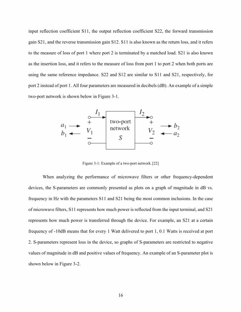
A microwave filter can be represented as a two-port network, a circuit with two pairs of
terminals that connect the network to external circuitry. These pairs of terminals are called ports
under the condition that the current entering one terminal is equal to the current exiting the second
terminal. Modeling a filter as a two-port network simplifies the analysis of the device by isolating
it from the rest of the circuit, leaving the device to be viewed as a “black box.” Two-port networks
can be analyzed using several different measures of performance—scattering (S) parameters,
ABCD parameters, and open-circuit impedance (Z) parameters, among others. In this work, S-
parameters of a metamaterial filter will be analyzed. The four S-parameters are as follows: the
16
input reflection coefficient S11, the output reflection coefficient S22, the forward transmission
gain S21, and the reverse transmission gain S12. S11 is also known as the return loss, and it refers
to the measure of loss of port 1 where port 2 is terminated by a matched load. S21 is also known
as the insertion loss, and it refers to the measure of loss from port 1 to port 2 when both ports are
using the same reference impedance. S22 and S12 are similar to S11 and S21, respectively, for
port 2 instead of port 1. All four parameters are measured in decibels (dB). An example of a simple
two-port network is shown below in Figure 3-1.
Figure 3-1: Example of a two-port network. [22]
When analyzing the performance of microwave filters or other frequency-dependent
devices, the S-parameters are commonly presented as plots on a graph of magnitude in dB vs.
frequency in Hz with the parameters S11 and S21 being the most common inclusions. In the case
of microwave filters, S11 represents how much power is reflected from the input terminal, and S21
represents how much power is transferred through the device. For example, an S21 at a certain
frequency of -10dB means that for every 1 Watt delivered to port 1, 0.1 Watts is received at port
2. S-parameters represent loss in the device, so graphs of S-parameters are restricted to negative
values of magnitude in dB and positive values of frequency. An example of an S-parameter plot is
shown below in Figure 3-2.
17
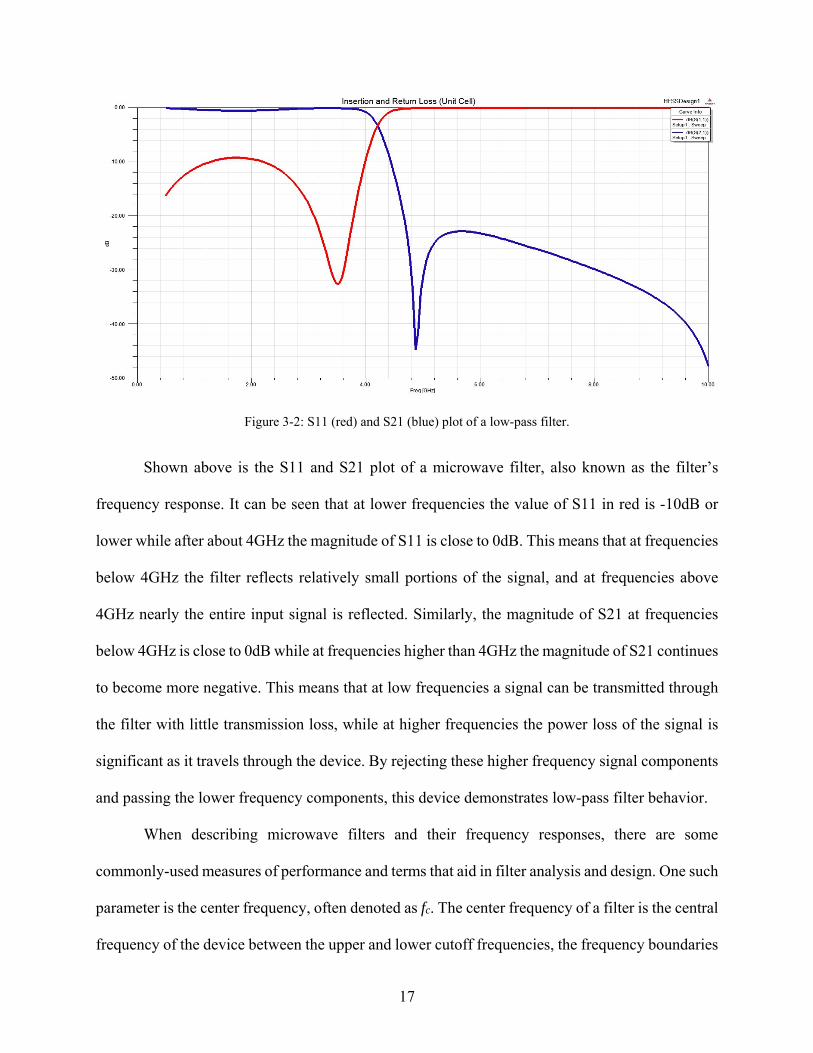
Figure 3-2: S11 (red) and S21 (blue) plot of a low-pass filter.
Shown above is the S11 and S21 plot of a microwave filter, also known as the filter’s
frequency response. It can be seen that at lower frequencies the value of S11 in red is -10dB or
lower while after about 4GHz the magnitude of S11 is close to 0dB. This means that at frequencies
below 4GHz the filter reflects relatively small portions of the signal, and at frequencies above
4GHz nearly the entire input signal is reflected. Similarly, the magnitude of S21 at frequencies
below 4GHz is close to 0dB while at frequencies higher than 4GHz the magnitude of S21 continues
to become more negative. This means that at low frequencies a signal can be transmitted through
the filter with little transmission loss, while at higher frequencies the power loss of the signal is
significant as it travels through the device. By rejecting these higher frequency signal components
and passing the lower frequency components, this device demonstrates low-pass filter behavior.
When describing microwave filters and their frequency responses, there are some
commonly-used measures of performance and terms that aid in filter analysis and design. One such
parameter is the center frequency, often denoted as fc. The center frequency of a filter is the central
frequency of the device between the upper and lower cutoff frequencies, the frequency boundaries

18
where the response changes from a passband to a stopband or vice versa. The cutoff frequencies
often define the frequency region where the device acts in a desired manner, otherwise known as
the bandwidth. The bandwidth most common in filter analysis is the -3dB bandwidth, where the
cutoff frequencies are defined at the points on the graph where the S-parameter magnitude is -3dB,
signifying a point where the power of the signal is one-half the maximum power.
Passive RF and microwave filters are often represented by lumped element models—
circuits composed of series and parallel or shunt combinations of capacitor and inductor
components. These lumped element models are usually presented as one of two dual types of
network configurations, namely the T-section network and the π-section network. An example of
a T-section network and a π-section network are shown below in Figure 3-3.
Figure 3-3: T-section and π-section models of a lumped element filter.
The T-section network starts with a series element that is connected on a single end to both
a shunt element and another series element, making a “T” shape. Similarly, the π-section model
begins with a shunt element connected to a series element that is also connected to another shunt
element on the opposite end, making a sort of “π” shaped network. Both T-section and π-section
models are generally symmetrical and contain an odd number of elements in order to take
advantage of this symmetry.
19
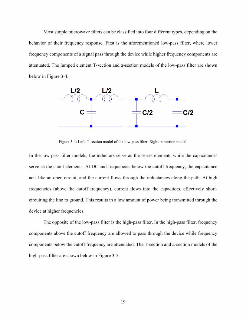
Most simple microwave filters can be classified into four different types, depending on the
behavior of their frequency response. First is the aforementioned low-pass filter, where lower
frequency components of a signal pass through the device while higher frequency components are
attenuated. The lumped element T-section and π-section models of the low-pass filter are shown
below in Figure 3-4.
Figure 3-4: Left: T-section model of the low-pass filter. Right: π-section model.
In the low-pass filter models, the inductors serve as the series elements while the capacitances
serve as the shunt elements. At DC and frequencies below the cutoff frequency, the capacitance
acts like an open circuit, and the current flows through the inductances along the path. At high
frequencies (above the cutoff frequency), current flows into the capacitors, effectively short-
circuiting the line to ground. This results in a low amount of power being transmitted through the
device at higher frequencies.
The opposite of the low-pass filter is the high-pass filter. In the high-pass filter, frequency
components above the cutoff frequency are allowed to pass through the device while frequency
components below the cutoff frequency are attenuated. The T-section and π-section models of the
high-pass filter are shown below in Figure 3-5.

20
Figure 3-5: Left: T-section model of the high-pass filter. Right: π-section model.
In the high-pass filter model, the capacitance serves as the series element while the inductance
serves as the shunt element. At DC and low frequencies, the inductor in the model behaves like a
short-circuit to ground, preventing signal propagation. At higher frequencies, the inductor begins
to act as an open circuit and the signal propagates. The low-pass and high-pass filters are duals in
nature and can be transformed back and forth by replacing capacitances with inductances and
inductances with capacitances.
In addition to low-pass and high-pass filters, there exist also the band-stop or notch filter
and the band-pass filter. The band-stop filter is unique in that it is designed to allow all frequencies
from DC onward except for a certain band of interest. In this band, called the stopband, signal
propagation is impeded, while signal propagation is allowed elsewhere. In the band-pass filter, the
opposite is true—only a single band of interest is passed, while signal propagation at frequencies
both lower and higher than the cutoff frequencies is inhibited. Lumped element models of both the
band-stop and band-pass filters are shown below in Figure 3-6 and Figure 3-7.
21
Figure 3-6: Lumped element model of the band-stop filter.
Figure 3-7: Lumped element model of the band-pass filter.
It can be seen by the series arrangement of shunt combinations of capacitance and inductance that
the band-stop filter is designed to pass signal components at all frequencies except those around
the center frequency, while the series arrangement of series elements in the band-pass filter allows
the device to block out most frequency components except those around the center frequency.
22
Several different technologies have been proposed for the design of electronic filters.
Analog passive filters like those shown previously can be fabricated using simple arrangements of
sheets of metal that act as capacitive and inductive elements, and these filters, while simple, require
no power source to operate. Active analog filters can also be designed by adding powered
components like operational amplifiers. In addition to these simpler types of devices, some more
novel designs have been presented.
Digital filters have been realized and allow for operation on discrete-time signals as
opposed to the real-time signals used by analog filters. [23] Since software and microprocessors
can be introduced to the design of these digital filters, much more complex filter designs are
possible. Additionally, digital filters are not as vulnerable to component tolerances and errors. A
digital filter generally consists of an analog-to-digital converter to convert the analog signal to
some digital input, some computer program running on a processing unit to filter the data, and a
digital-to-analog converter to convert the digital output back to an analog signal. While digital
filters, especially higher order versions, can take up less space in a circuit, they are limited with
respect to analog filters by their power consumption, inherent latency, and noise and information
loss through the conversion processes.
Several types of mechanical filters have also been proposed. [24] These filters take
advantage of transducers at the input and output ports to convert electrical signals into mechanical
vibrations and vice versa. These filters are analogous to electronic filters in design and analysis
but are capable of achieving much higher values of quality factor Q and, subsequently, selectivity.
RF microeletrocmechanical systems (MEMS) filters, a subset of mechanical filters, is a relatively
recent technology in the design of mechanical filters and has made possible the construction of
high Q filters of small size. [25]

23
The surface acoustic wave (SAW) filter is an electromechanical device that combines
aspects of electronic and mechanical filters into one application. [26] An RF signal on the input
side is converted to an mechanical wave that travels across the surface of a substrate made of
ceramic, piezoelectric crystal, or a similar material. On the output end, a delayed version of the
signal is converted from an acoustic wave back to an RF signal. A similar device to the SAW filter
is the bulk acoustic wave (BAW) filter, which uses thin-film technology and standing waves to
filter at higher RF frequencies than SAW technology. [27]
To realize filters in microelectronic technology, one common approach is the planar
microstrip transmission line design. Microstrip offers several engineering advantages, including
ease of integration with active and passive devices, the ability to be micromachined using
photolithographic processes, compact size, light weight, and cost. In microstrip design, a flat metal
conducting strip (such as copper) is placed on a relatively large but electrically thin dielectric
substrate with a ground plane on the bottom. An example of a microstrip transmission line is shown
below in Figure 3-8.
Figure 3-8: A simple microstrip transmission line. [28]

24
The physical features of a microstrip transmission line play a large role in the performance
of the device. Sheets of metal on the substrate that compose the signal line can represent lumped
elements or combinations of lumped elements, depending on their shape. This allows for the
construction of microwave filters on a substrate without any actual lumped element components.
For example, an open-ended microstrip line can be represented as a transmission line terminated
in a capacitance. Microstrip filters often have signal lines that vary in width over the length of the
line with pieces of line of differing width and length attached to the main line. Two properties of
microstrip that are relevant to this work are the fact that series etched gaps in microstrip can be
modeled as a capacitance and shunt stubs of line can be represented as impedance. [29]
For the construction of metamaterial filters at RF and higher frequencies, special
consideration must be given to the type of dielectric substrates of these devices for various reasons
including cost, ease of fabrication, dielectric constant, RF properties, and in this case, flexibility.
In this work, all filter designs are presented using the microstrip transmission line filter approach
using a liquid crystal polymer (LCP) substrate. LCP is more commonly used in MEMS design
than in metamaterials, although there has been recent work using LCP as a metamaterial substrate.
[30] [31] LCP is chemically unreactive, has a low dielectric constant of 3.1, is mechanically strong,
is thermally stable, and is readily commercially available. A common use for solid LCP is in Kevlar
products, and when purchased from a manufacturer LCP is generally laminated on one or both
sides with copper cladding. LCP can reportedly be useful as a substrate for frequency applications
beyond 40GHz because it is not as lossy as conventional RF materials at higher frequencies. [32]
[33] In [33], it is claimed that LCP offers a low loss tangent at frequencies as high as 110GHz.
LCP can exist in both a liquid phase and a solid phase, but in its solid phase it can be treated
as a rigid structure for the purposes of micromachining and microelectronic fabrication while still
25
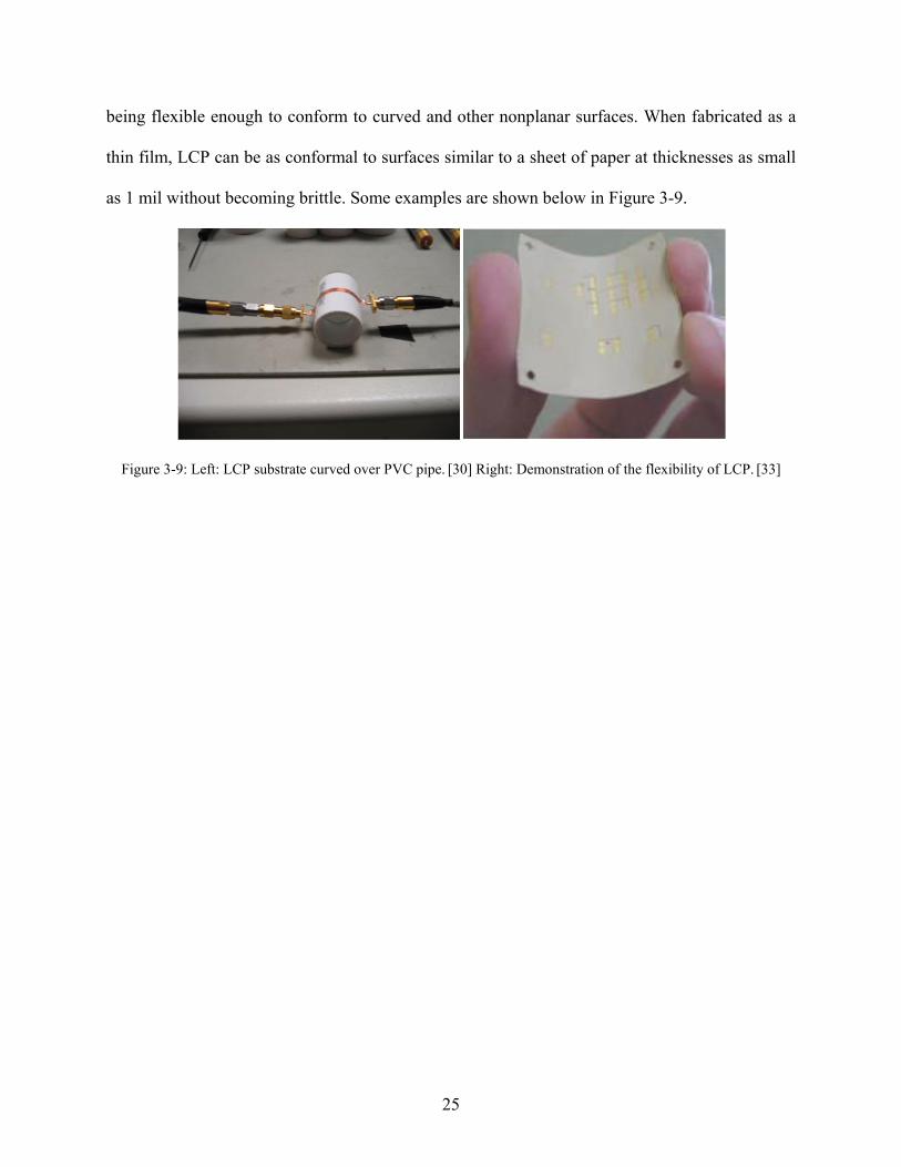
being flexible enough to conform to curved and other nonplanar surfaces. When fabricated as a
thin film, LCP can be as conformal to surfaces similar to a sheet of paper at thicknesses as small
as 1 mil without becoming brittle. Some examples are shown below in Figure 3-9.
Figure 3-9: Left: LCP substrate curved over PVC pipe. [30] Right: Demonstration of the flexibility of LCP. [33]
26
Chapter4 Metamaterial Filters
As mentioned in the previous chapter, transmission lines laden with resonating
metamaterial elements experience backward wave propagation due to negative index of refraction
over a certain frequency range defined by the structure of the device. In this sense, a metamaterial
device can be considered a frequency-selective structure (FSS), a periodic structure that responds
to electromagnetic fields based on frequency. At certain frequencies, current induced in an FSS
will transmit power from an incident wave through the structure; however, at other frequencies the
FSS will inhibit or reflect an incident wave. Because of this behavior, FSSs are often considered a
type of filter.
Due to their resonant nature, compact size, straightforward implementation, and ease of
fabrication, metamaterial structures have become a common choice for novel RF and microwave
planar filter designs. Indeed, simply loading a transmission line with SRRs or CSRRs will inhibit
wave propagation near the resonant frequency due to the negative-index nature of the resonant
elements. In the SRR case, the addition of shunt stubs will generate backward wave propagation,
and the same effect can be accomplished in the CSRR case using etched series gaps instead. In
addition to this, it is possible to combine shunt stubs and series gaps in a metamaterial transmission
line to achieve well-known types of filters—different configurations of these stubs and gaps can
be used to realize low-pass filters (LPF), high-pass filters (HPF), band-stop filters (BSF), and band-
pass filters (BPF). Over time, patterns have emerged in the design of these types of filters, making
it easy to determine the type of a metamaterial filter by observing the presence or lack of shunt
stubs and series gaps in the signal line. In this work, the design of CSRR-loaded RF and microwave
metamaterial filters using microstrip technology will be examined exclusively.
27
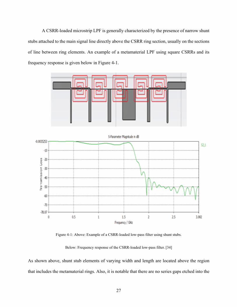
A CSRR-loaded microstrip LPF is generally characterized by the presence of narrow shunt
stubs attached to the main signal line directly above the CSRR ring section, usually on the sections
of line between ring elements. An example of a metamaterial LPF using square CSRRs and its
frequency response is given below in Figure 4-1.
Figure 4-1: Above: Example of a CSRR-loaded low-pass filter using shunt stubs.
Below: Frequency response of the CSRR-loaded low-pass filter. [34]
As shown above, shunt stub elements of varying width and length are located above the region
that includes the metamaterial rings. Also, it is notable that there are no series gaps etched into the
28
signal line in the LPF, although the signal line does visibly narrow and widen over the CSRR
region.
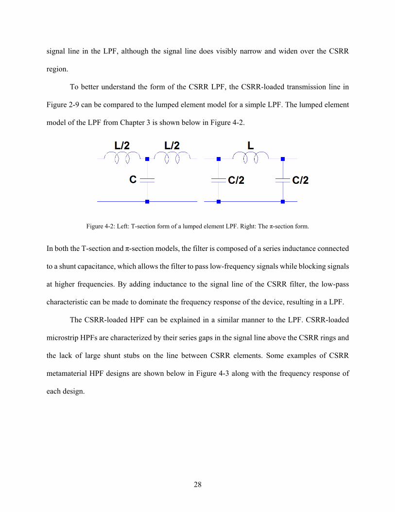
To better understand the form of the CSRR LPF, the CSRR-loaded transmission line in
Figure 2-9 can be compared to the lumped element model for a simple LPF. The lumped element
model of the LPF from Chapter 3 is shown below in Figure 4-2.
Figure 4-2: Left: T-section form of a lumped element LPF. Right: The π-section form.
In both the T-section and π-section models, the filter is composed of a series inductance connected
to a shunt capacitance, which allows the filter to pass low-frequency signals while blocking signals
at higher frequencies. By adding inductance to the signal line of the CSRR filter, the low-pass
characteristic can be made to dominate the frequency response of the device, resulting in a LPF.
The CSRR-loaded HPF can be explained in a similar manner to the LPF. CSRR-loaded
microstrip HPFs are characterized by their series gaps in the signal line above the CSRR rings and
the lack of large shunt stubs on the line between CSRR elements. Some examples of CSRR
metamaterial HPF designs are shown below in Figure 4-3 along with the frequency response of
each design.
29
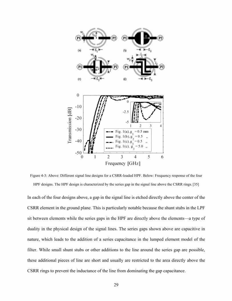
Figure 4-3: Above: Different signal line designs for a CSRR-loaded HPF. Below: Frequency response of the four
HPF designs. The HPF design is characterized by the series gap in the signal line above the CSRR rings. [35]
In each of the four designs above, a gap in the signal line is etched directly above the center of the
CSRR element in the ground plane. This is particularly notable because the shunt stubs in the LPF
sit between elements while the series gaps in the HPF are directly above the elements—a type of
duality in the physical design of the signal lines. The series gaps shown above are capacitive in
nature, which leads to the addition of a series capacitance in the lumped element model of the
filter. While small shunt stubs or other additions to the line around the series gap are possible,
these additional pieces of line are short and usually are restricted to the area directly above the
CSRR rings to prevent the inductance of the line from dominating the gap capacitance.

30
For the HPF case, the lumped element model of the HPF from Chapter 3 is shown below
in Figure 4-4.
Figure 4-4: Left: T-section from of a lumped element HPF. Right: π-section form.
Comparing the models in Figure 4-4 to that in Figure 2-9, it can be seen that the capacitive gap Cg
serves as the series capacitance in the CSRR high-pass model. In the design, this capacitance
allows the high-pass component of the filter to dominate the frequency response in the negative-
index region, resulting in a CSRR-loaded HPF.
While the LPF and HPF require adding material to or removing material from the host line,
designing the metamaterial band-stop filter using CSRRs is relatively simple. While the low-pass
and high-pass filter designs seem to require additions or subtractions to the host line, it has been
shown that a band-stop filter can be realized by simply etching CSRR rings underneath a microstrip
transmission line and substrate [36]. Using no series etched gaps or shunt stubs, a narrowband stop-
band filter was designed where the three CSRR elements were located at symmetric periodic points
in the ground plane. A picture of the band-stop filter design is shown below in Figure 4-5.
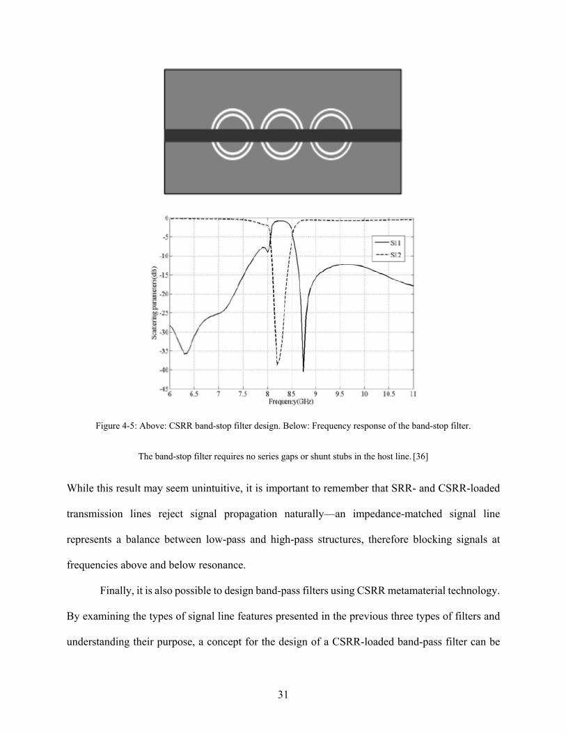
31
Figure 4-5: Above: CSRR band-stop filter design. Below: Frequency response of the band-stop filter.
The band-stop filter requires no series gaps or shunt stubs in the host line. [36]
While this result may seem unintuitive, it is important to remember that SRR- and CSRR-loaded
transmission lines reject signal propagation naturally—an impedance-matched signal line
represents a balance between low-pass and high-pass structures, therefore blocking signals at
frequencies above and below resonance.
Finally, it is also possible to design band-pass filters using CSRR metamaterial technology.
By examining the types of signal line features presented in the previous three types of filters and
understanding their purpose, a concept for the design of a CSRR-loaded band-pass filter can be
32
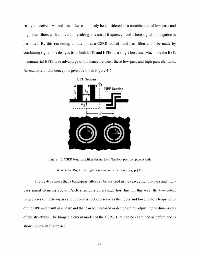
easily conceived. A band-pass filter can loosely be considered as a combination of low-pass and
high-pass filters with an overlap resulting in a small frequency band where signal propagation is
permitted. By this reasoning, an attempt at a CSRR-loaded band-pass filter could be made by
combining signal line designs from both LPFs and HPFs on a single host line. Much like the BSF,
metamaterial BPFs take advantage of a balance between these low-pass and high-pass elements.
An example of this concept is given below in Figure 4-6.
Figure 4-6: CSRR band-pass filter design. Left: The low-pass component with
shunt stubs. Right: The high-pass component with series gap. [35]
Figure 4-6 shows that a band-pass filter can be realized using cascading low-pass and high-
pass signal elements above CSRR structures on a single host line. In this way, the two cutoff
frequencies of the low-pass and high-pass sections serve as the upper and lower cutoff frequencies
of the BPF and result in a passband that can be increased or decreased by adjusting the dimensions
of the structures. The lumped element model of the CSRR BPF can be examined as before and is
shown below in Figure 4-7.

33
Figure 4-7: Lumped element model of the CSRR-loaded BPF.
In the lumped element model above, L represents the inductance of the host line, Cg
represents the capacitance of the etched gap, Cc models the electric coupling capacitance, Lr
represents the ring inductance, and Cr models the ring capacitance. As explained earlier, when
adding etched capacitance to a CSRR-loaded transmission line, the capacitance will dominate the
frequency response at the resonant frequency, resulting in a HPF. In this instance, the CSRR-
loaded HPF can be converted to a BPF by increasing the inductance of the filter at resonance. This
can be achieved by adding shunt stubs of line from the LPF design concept to increase the line
inductance.
Since the behavior of the CSRR-loaded BPF can be easily adjusted, this filter in particular
leaves the designer with the ability to finely tune the frequency response of the device. In [36], a
metamaterial BPF was designed with cutoff as sharp as 50 dB at the lower and upper cutoff
frequencies. The frequency response is shown below in Figure 4-8.
34
Figure 4-8: Frequency response of a CSRR-loaded band-pass filter. [35]
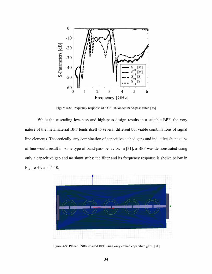
While the cascading low-pass and high-pass design results in a suitable BPF, the very
nature of the metamaterial BPF lends itself to several different but viable combinations of signal
line elements. Theoretically, any combination of capacitive etched gaps and inductive shunt stubs
of line would result in some type of band-pass behavior. In [31], a BPF was demonstrated using
only a capacitive gap and no shunt stubs; the filter and its frequency response is shown below in
Figure 4-9 and 4-10.
Figure 4-9: Planar CSRR-loaded BPF using only etched capacitive gaps. [31]

35
Figure 4-10: Frequency response of the BPF shown in Figure 4-9. [31]
In [37], a BPF was designed that used only a single signal line element combining series gaps and
shunt stubs above a CSRR. This design incorporated additional capacitive gaps and inductive lines
on the signal line in an attempt to sharpen the upper band performance of the frequency response
and inspired the design presented in this work. The filter and its frequency response are shown in
Figure 4-11 and Figure 4-12.
Figure 4-11: CSRR-loaded BPF with a single element above the metamaterial structure. [37]

36
Figure 4-12: Simulated and measured frequency response of the BPF shown in Figure 4-11. [37]

37
Chapter5 HFSS
In this work, Ansys HFSS was used to design and simulate all metamaterial filter models.
This commercial electromagnetic modeling and simulation software uses the Finite Element
Method (FEM) to solve three-dimensional microwave structures such as antennas, transmission
lines, oscillators, and in this case filters. In HFSS, the user is able to draw a structure using
predefined shapes such as boxes, spheres, and cylinders, create custom shapes using several editing
options, and simulate an extensive list of electromagnetic parameters such as S-parameters over
variables such as frequency or physical dimensions. HFSS is also able to show and animate
electromagnetic fields traveling through and across a device in both magnitude and vector forms.
To simulate a structure, the user must define the boundaries and excitations of the model after
selecting a solution type. HFSS then uses an iterative solving approach that includes creating
meshes and updating the solution by solving adaptive passes over the full frequency spectrum of
interest. A short overview of the design and simulation of a simple metamaterial filter will be given
in this chapter.
To begin the design of the filter model, the ground plane will be added first. This is done
by selecting a "box" shape from the 3D Modeler Draw Solid toolbar. This box must then be added
to the model by drawing the box shape in the main design window. First the user must click a point
in the drawing window to place one corner, then expand to a two-dimensional plane, then add the
third dimension; each step automatically occurs after the previous one when the user clicks the
desired location. After placing the box, the shape will appear under "Solids" in the explorer
window to the left of the design space. Double left-clicking the default name "CreateBox" will
allow the user to change the position of the object and its size in all three dimensions. For this
38
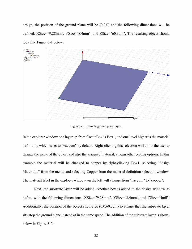
design, the position of the ground plane will be (0,0,0) and the following dimensions will be
defined: XSize="9.28mm", YSize="8.4mm", and ZSize="60.3um". The resulting object should
look like Figure 5-1 below.
Figure 5-1: Example ground plane layer.
In the explorer window one layer up from CreateBox is Box1, and one level higher is the material
definition, which is set to "vacuum" by default. Right-clicking this selection will allow the user to
change the name of the object and also the assigned material, among other editing options. In this
example the material will be changed to copper by right-clicking Box1, selecting "Assign
Material..." from the menu, and selecting Copper from the material definition selection window.
The material label in the explorer window on the left will change from "vacuum" to "copper".
Next, the substrate layer will be added. Another box is added to the design window as
before with the following dimensions: XSize="9.28mm", YSize="8.4mm", and ZSize="4mil".
Additionally, the position of the object should be (0,0,60.3um) to ensure that the substrate layer
sits atop the ground plane instead of in the same space. The addition of the substrate layer is shown
below in Figure 5-2.

39
Figure 5-2: Example filter design with added LCP substrate layer.
To define the substrate as LCP, a custom material definition must be added. In the material
definition window, select the "Add Material..." button at the bottom. In the View/Edit Material
window, set Relative Permittivity to 3.1, Relative Permeability to 1, and Dielectric Loss Tangent
to 0.004 for LCP. Name the material LCP and hit OK. Now the substrate layer can be defined as
LCP.
Next, the signal line must be added to the model. In this design, a transmission line
calculator was used to set the signal line dimensions to match the rest of the microstrip device. For
the signal line, define the material as "copper", set the position to (4.176mm,0,0.1619mm) to place
the signal layer on top of the substrate and in the middle of the device, and set the following
dimensions: XSize="928um", YSize="8.4mm", and ZSize="60.3um". The object should look like
Figure 5-3 below.

40
Figure 5-3: Example filter design with copper signal line added.
Next, the metamaterial CSRR rings will be added to the design. To create the rings, two
cylinders must be created and then subtracted from the ground plane. Select the Draw Cylinder
button next to the Draw Box button and place the cylinder on the device. Right click the cylinder
in the explorer window and add the following information: Center Position (4.64mm,4.2mm,0),
Radius="3.432mm", and Height="60.3um". This will place the cylinder at the center of the device
and will define it as the same height as the ground plane. Define the material of the cylinder as
"copper", then add another cylinder using the same process. Right click the second cylinder in the
explorer window and define the shape as follows: Center Position (4.64mm,4.2mm,0),
Radius="2.7615mm", and Height="60.3um". The two cylinders in the model should look like
Figure 5-4 below.

41
Figure 5-4: Example filter design with both cylinders added for the outer ring.
Next, the smaller cylinder must be subtracted from the larger cylinder to create a ring. To
do this, select Cylinder1 and Cylinder2 while holding the CTRL button on the keyboard. Right
click Cylinder2, and in the menu go to "Edit">"Boolean">"Subtract...". In the Subtract window,
ensure that Cylinder1 is on the left side under "Blank Parts" while Cylinder2 is on the right side
under "Tool Parts". Click OK and the smaller cylinder should be removed from the larger cylinder
shape, leaving a ring in the ground plane of the device. This ring is shown below in Figure 5-5.
Figure 5-5: Example filter design with the outside CSRR ring shape.

42
To create the inner CSRR ring, a similar process is used. Create the outer cylinder of the inner ring
with the following properties: Center Position (4.64mm,4.2mm,0), Radius="1.2275mm", and
Height="60.3um". Create a second cylinder with Center Position (4.64mm,4.2mm,0), Radius
="0.9615mm", and Height="60.3um". Subtract the inner cylinder from the outer cylinder as
before, and the device should now look like Figure 5-6 below.
Figure 5-6: Example filter design with both outer and inner CSRR ring shapes.
Next, the ring gaps must be removed from the ring shapes. This will be accomplished by
adding two box shapes to the device, one on each ring on opposing sides. Click the Draw Box
button and add two boxes to the device. For the outer ring gap, use the following properties:
Position (1.208mm,3.35625mm,0mm), XSize="1000um", YSize="1687.5um", and
Zsize="60.3um". For the inner ring gap, use the following properties: Position (5.869mm,
3.35625mm0mm), XSize="-1000um", YSize="1687.5um", and ZSize="60.3um". Use

43
Edit>Boolean>Subtract to remove the boxes from the two rings, and the device should now look
like Figure 5-7 below.
Figure 5-7: Example filter design with ring gaps added.
Finally, the two metamaterial rings must be subtracted from the ground plane to simulate
the etching that is done in the fabrication process. Simply select the two rings and go to
Edit>Boolean> Subtract and remove the two rings from the ground plane. The end result should
look like Figure 5-8 below (the substrate layer has been made transparent so that the rings can be
easily seen).
Figure 5-8: Example filter design with CSRR rings removed from the ground plane.
44
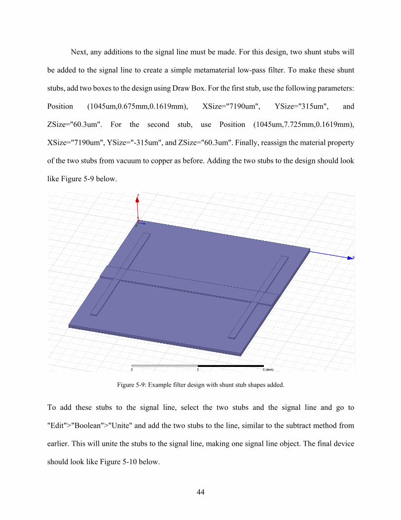
Next, any additions to the signal line must be made. For this design, two shunt stubs will
be added to the signal line to create a simple metamaterial low-pass filter. To make these shunt
stubs, add two boxes to the design using Draw Box. For the first stub, use the following parameters:
Position (1045um,0.675mm,0.1619mm), XSize="7190um", YSize="315um", and
ZSize="60.3um". For the second stub, use Position (1045um,7.725mm,0.1619mm),
XSize="7190um", YSize="-315um", and ZSize="60.3um". Finally, reassign the material property
of the two stubs from vacuum to copper as before. Adding the two stubs to the design should look
like Figure 5-9 below.
Figure 5-9: Example filter design with shunt stub shapes added.
To add these stubs to the signal line, select the two stubs and the signal line and go to
"Edit">"Boolean">"Unite" and add the two stubs to the line, similar to the subtract method from
earlier. This will unite the stubs to the signal line, making one signal line object. The final device
should look like Figure 5-10 below.

45
Figure 5-10: Final model of the example filter design.
To simulate the filter, a few external objects must be added to the design. First, a region
must be created around the filter to define the simulation region. Click the red and white Create
Region button at the right end of the 3D Modeler Draw Objects toolbar. In the new Region
window, select the "Pad individual directions" option and set +Z and -Z to "Absolute Position".
For +Z set the value to 5mm, and for -Z set the value to -5mm. This will create a vacuum box
region that will surround the filter and allow 5mm of space above and below the device. An
example is shown below in Figure 5-11.
Figure 5-11: Example filter design with boundary region added.

46
To finishing defining the simulation region, right click the region box and select "Assign
Boundary">"Radiation" and click OK.
Next, the two port planes must be added to the terminating sides of the signal line. Click
the yellow Draw Rectangle button from the 3D Modeler Draw Sheet toolbar and draw two
rectangles, one on each signal line end of the filter. Note that the active plane to draw 2D structures
is set to XY, so this may need to be changed to ZX to draw the plane correctly. This can be done
by selecting ZX from the drop down menu beside the Draw Region button used previously. The
first rectangle should be at position (0,0,0) with an XSize of 9280um and ZSize of 32mil, and the
second rectangle should be at position (0,8.4mm,0) with the same XSize and ZSize as the first
rectangle. After adding the two ports, the filter design should look like Figure 5-12 below.
Figure 5-12: Example filter design with port shapes added.
47
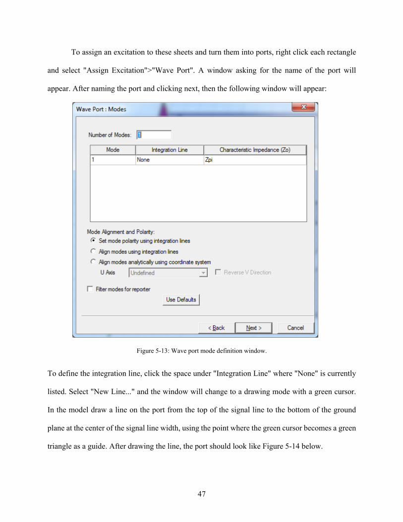
To assign an excitation to these sheets and turn them into ports, right click each rectangle
and select "Assign Excitation">"Wave Port". A window asking for the name of the port will
appear. After naming the port and clicking next, then the following window will appear:
Figure 5-13: Wave port mode definition window.
To define the integration line, click the space under "Integration Line" where "None" is currently
listed. Select "New Line..." and the window will change to a drawing mode with a green cursor.
In the model draw a line on the port from the top of the signal line to the bottom of the ground
plane at the center of the signal line width, using the point where the green cursor becomes a green
triangle as a guide. After drawing the line, the port should look like Figure 5-14 below.

48
Figure 5-14: Integration line drawn from the signal line to the ground plane, represented by the red arrow.
In the next window, select "Renormalize All Modes" and select 50 ohm for the Full Port
Impedance to match the ports to 50Ω. Repeat this process for the second port to define both
excitation ports.
After setting the excitation ports, right-click Analysis in the Project Manager pane and click
Add Solution Step. For this example, set the Solution Frequency to 4.2GHz and use a Maximum
Number of Passes of 12 and a Maximum Delta S of 0.05. The solution frequency needs to be close
to the resonant frequency of the device, so this step may require some iteration once a simulation
is run to get an accurate solution. The maximum number of passes determines how many adaptive
passes will be made to converge the solution, and the maximum delta S determines the allowed
solution error.
Next, in the upper toolbar click the Add Frequency Sweep button that looks like a red line
on a graph. This allows the user to define the parameters of the frequency sweep for the simulation.
49
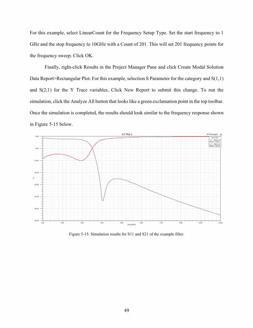
For this example, select LinearCount for the Frequency Setup Type. Set the start frequency to 1
GHz and the stop frequency to 10GHz with a Count of 201. This will set 201 frequency points for
the frequency sweep. Click OK.
Finally, right-click Results in the Project Manager Pane and click Create Modal Solution
Data Report>Rectangular Plot. For this example, selection S Parameter for the category and S(1,1)
and S(2,1) for the Y Trace variables. Click New Report to submit this change. To run the
simulation, click the Analyze All button that looks like a green exclamation point in the top toolbar.
Once the simulation is completed, the results should look similar to the frequency response shown
in Figure 5-15 below.
Figure 5-15: Simulation results for S11 and S21 of the example filter.
1.00 2.00 3.00 4.00 5.00 6.00 7.00 8.00 9.00 10.00Freq [GHz]
-35.00
-30.00
-25.00
-20.00
-15.00
-10.00
-5.00
0.00
Y1
HFSSDesign2XY Plot 1 ANSOFT
Curve Info
dB(S(1,1))Setup1 : Sw eep
dB(S(2,1))Setup1 : Sw eep
50
Chapter6 Improved BPF Design
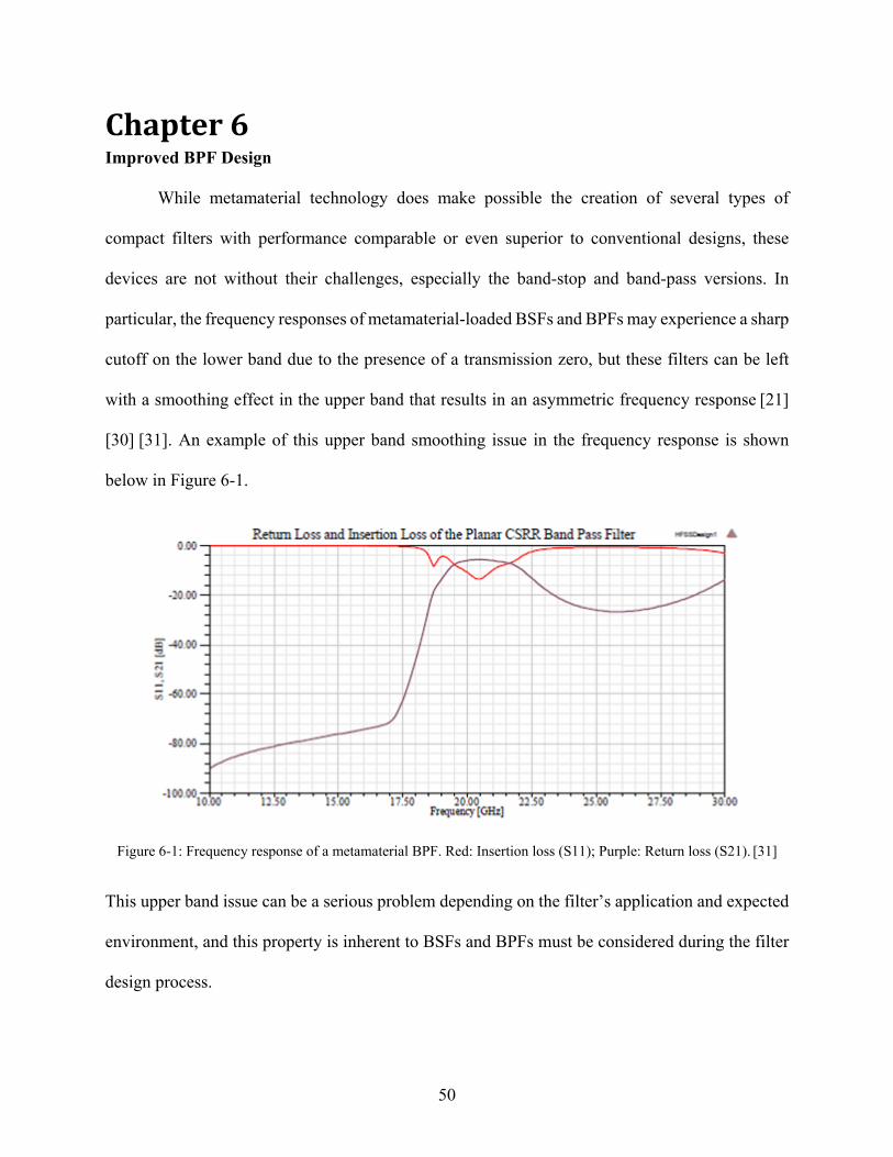
While metamaterial technology does make possible the creation of several types of
compact filters with performance comparable or even superior to conventional designs, these
devices are not without their challenges, especially the band-stop and band-pass versions. In
particular, the frequency responses of metamaterial-loaded BSFs and BPFs may experience a sharp
cutoff on the lower band due to the presence of a transmission zero, but these filters can be left
with a smoothing effect in the upper band that results in an asymmetric frequency response [21]
[30] [31]. An example of this upper band smoothing issue in the frequency response is shown
below in Figure 6-1.
Figure 6-1: Frequency response of a metamaterial BPF. Red: Insertion loss (S11); Purple: Return loss (S21). [31]
This upper band issue can be a serious problem depending on the filter’s application and expected
environment, and this property is inherent to BSFs and BPFs must be considered during the filter
design process.

51
In this work, an attempt has been made to mitigate this upper band smoothing problem in
a CSRR-loaded BPF based on previous work at Auburn University [30] [31]. This was achieved
by introducing a unique signal line design concept to the BPF that combines the shunt stub trait of
the LPF with the series gap trait of the HPF, resulting in a single signal line element to act as a
band-pass filter. Additional shunt inductance was added to increase the low-pass component of the
filter and suppress the frequency response in the upper band in order to achieve symmetrical band-
pass behavior. As with previous work, this filter was designed using an LCP substrate to realize a
flexible filter for nonplanar surface applications. The design of this filter will be the focus of the
rest of this chapter.
In [31], a planar band-pass filter using an LCP substrate was presented using periodic series
capacitive gaps etched into the signal line. These gaps were placed at the center of the CSRR
elements underneath the substrate and etched into the ground plane. The filter is shown below in
Figure 6-2, and its frequency response is shown previously in Figure 6-1.
Figure 6-2: Metamaterial BPF using series etched capacitive gaps. [31]

52
To design a BPF with an improved upper band, a unit cell approach was taken. A unit cell
design can be a simple starting point for the design of a higher order metamaterial filter due to the
periodic nature of metamaterials. Cascading these unit cells, spaced apart an appropriate distance,
will result in a filter that has behavior similar to, but better defined than, that of the unit cell. To
design the unit cell, first a simple microstrip design was modeled in HFSS including the copper
signal line, an LCP substrate and the copper ground plane. The basis for the new BPF is shown
below in Figure 6-3.
Figure 6-3: Simple microstrip design for the unit cell including the signal line, LCP substrate, and ground plane.
In the model, the signal line was matched to 50Ω using a transmission line calculator and
has a width of 9.28mm, a height of 60.3µm, and a length of 8.4mm. The LCP substrate is also
8.4mm long and has a width of 9.28mm and a height of 4 mil. Finally, the copper cladding that
serves as the ground plane is 8.4mm in length, 9.28mm wide, and 60.3µm tall. The LCP substrate
has a relative permittivity of 3.1, and the copper is defined as having a relative permeability
of 0.999991.

53
Next, the CSRR rings were added to the ground plane. This was achieved by subtracting
two concentric cylinders from the ground plane and using a small rectangle shape subtracted from
the rings to create the ring gap. The filter model with the rings included is shown in Figure 6-4.
Figure 6-4: CSRR-loaded BPF model with CSRR rings etched into the ground plane.
In the model, the outer radius of the outer ring is 3.432mm, and the width of the outer ring
is about 0.671mm. The outer radius of the inner ring is about 1.23mm, and the width of the inner
ring is about 0.2685mm. The ring gaps are of equal length and are 1.6875mm long.
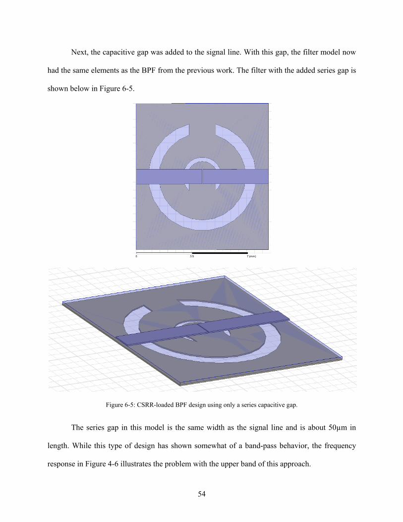
54
Next, the capacitive gap was added to the signal line. With this gap, the filter model now
had the same elements as the BPF from the previous work. The filter with the added series gap is
shown below in Figure 6-5.
Figure 6-5: CSRR-loaded BPF design using only a series capacitive gap.
The series gap in this model is the same width as the signal line and is about 50µm in
length. While this type of design has shown somewhat of a band-pass behavior, the frequency
response in Figure 4-6 illustrates the problem with the upper band of this approach.
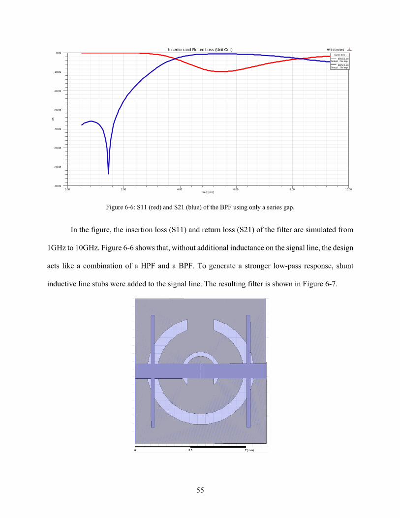
55
Figure 6-6: S11 (red) and S21 (blue) of the BPF using only a series gap.
In the figure, the insertion loss (S11) and return loss (S21) of the filter are simulated from
1GHz to 10GHz. Figure 6-6 shows that, without additional inductance on the signal line, the design
acts like a combination of a HPF and a BPF. To generate a stronger low-pass response, shunt
inductive line stubs were added to the signal line. The resulting filter is shown in Figure 6-7.
0.00 2.00 4.00 6.00 8.00 10.00Freq [GHz]
-70.00
-60.00
-50.00
-40.00
-30.00
-20.00
-10.00
0.00d
BHFSSDesign1Insertion and Return Loss (Unit Cell) ANSOFT
Curve Info
dB(S(1,1))Setup1 : Sw eep
dB(S(2,1))Setup1 : Sw eep
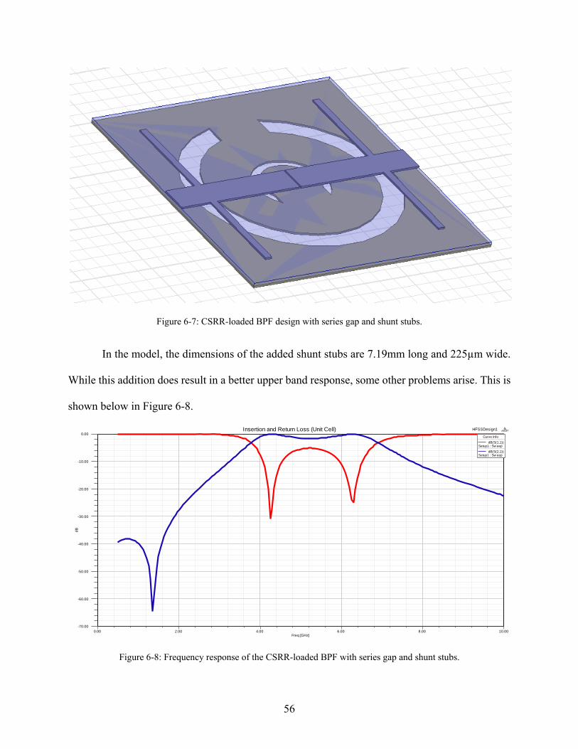
56
Figure 6-7: CSRR-loaded BPF design with series gap and shunt stubs.
In the model, the dimensions of the added shunt stubs are 7.19mm long and 225µm wide.
While this addition does result in a better upper band response, some other problems arise. This is
shown below in Figure 6-8.
Figure 6-8: Frequency response of the CSRR-loaded BPF with series gap and shunt stubs.
0.00 2.00 4.00 6.00 8.00 10.00Freq [GHz]
-70.00
-60.00
-50.00
-40.00
-30.00
-20.00
-10.00
0.00
dB
HFSSDesign1Insertion and Return Loss (Unit Cell) ANSOFT
Curve Info
dB(S(1,1))Setup1 : Sw eep
dB(S(2,1))Setup1 : Sw eep
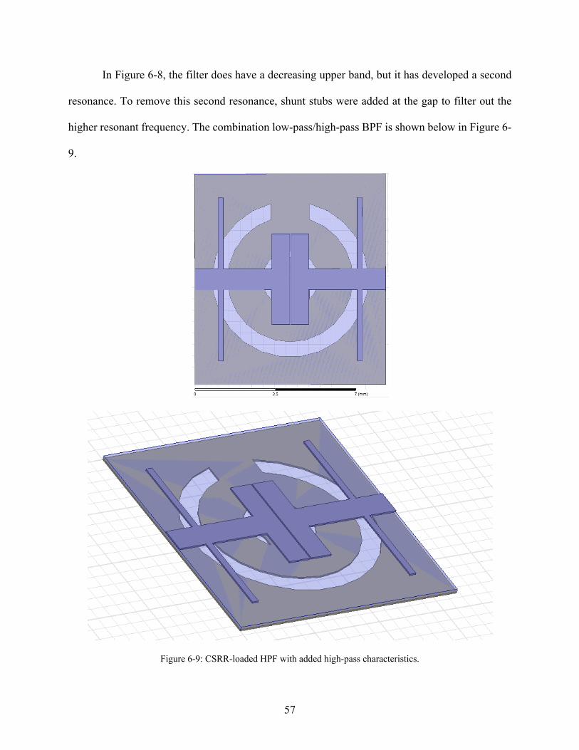
57
In Figure 6-8, the filter does have a decreasing upper band, but it has developed a second
resonance. To remove this second resonance, shunt stubs were added at the gap to filter out the
higher resonant frequency. The combination low-pass/high-pass BPF is shown below in Figure 6-
9.
Figure 6-9: CSRR-loaded HPF with added high-pass characteristics.
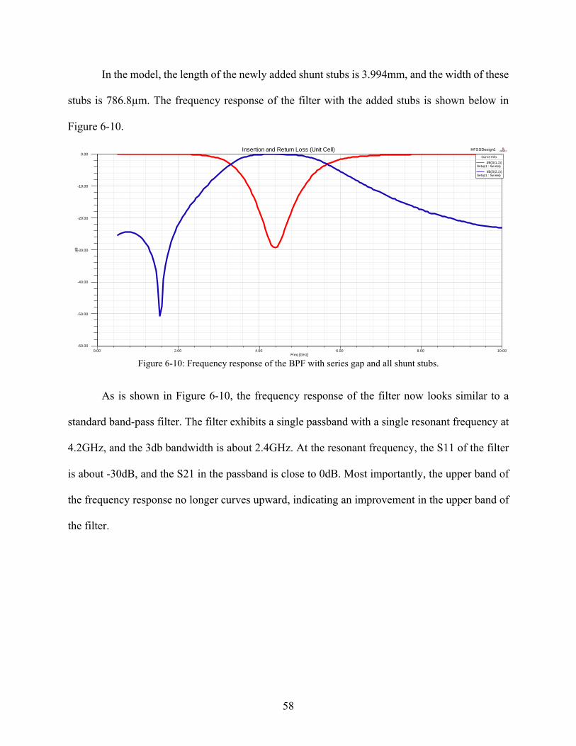
58
In the model, the length of the newly added shunt stubs is 3.994mm, and the width of these
stubs is 786.8µm. The frequency response of the filter with the added stubs is shown below in
Figure 6-10.
Figure 6-10: Frequency response of the BPF with series gap and all shunt stubs.
As is shown in Figure 6-10, the frequency response of the filter now looks similar to a
standard band-pass filter. The filter exhibits a single passband with a single resonant frequency at
4.2GHz, and the 3db bandwidth is about 2.4GHz. At the resonant frequency, the S11 of the filter
is about -30dB, and the S21 in the passband is close to 0dB. Most importantly, the upper band of
the frequency response no longer curves upward, indicating an improvement in the upper band of
the filter.
0.00 2.00 4.00 6.00 8.00 10.00Freq [GHz]
-60.00
-50.00
-40.00
-30.00
-20.00
-10.00
0.00
dB
HFSSDesign1Insertion and Return Loss (Unit Cell) ANSOFT
Curve Info
dB(S(1,1))Setup1 : Sw eep
dB(S(2,1))Setup1 : Sw eep
59
Chapter7 Conclusion
Novel microwave filters made from transmission lines loaded with metamaterial structures
called complementary split-ring resonators are easily realizable by adding these resonating rings
to the ground plane of a microstrip line. At least four different types of filters are possible—low-
pass, high-pass, band-stop, and band-pass filters. Band-stop and band-pass filters, however,
experience a smoothing effect in the upper band of the frequency response that has a negative
effect on filter performance. To correct this smoothing issue, the circuit models of the CSRR-
loaded low-pass and high-pass filters have been examined in an attempt to improve a previous
band-pass design.
By combining low-pass and high-pass concepts, a metamaterial band-pass filter has been
designed using HFSS. While the previous design used high-pass concepts in the form of etched
series capacitive gaps, shunt inductive stubs were not included originally. Adding shunt inductance
to the signal line increases the low-pass component of the filter. As shown in the simulation results,
this addition of shunt inductive stubs brought down the smoothed curve in the upper frequency
band, resulting in a frequency response that shows better band-pass filter behavior. By designing
the filter on LCP substrate, the fabrication of a high-order flexible band-pass filter that, based on
previous work, would show little degradation in performance over a given radius of curvature is
possible.

60
Chapter8 Future Work
Having designed a unit cell of a CSRR-loaded band-pass filter, the next step in refining
this design would be to expand this unit cell into a high-order filter by cascading several elements
in series. This would sharpen the frequency response behavior of the filter. Additionally, the
simulation results of this work could be verified by fabricating the design and testing a physical
realization of the model. In the future, filters like the one presented in this work could be used in
the design of advanced compact microwave filters and other microelectronic communication
technology.
61
Bibliography
[1] V. G. Veselago, "The electrodynamics of substances with simultaneously negative values of ε and μ," Sov. Phys. Usp., vol. 10, pp. 509-514, Jan-Feb 1968.
[2] R. A. Shelby, D. R. Smith and S. Schultz, "Experimental verification of a negative index of refraction," Science, vol. 292, pp. 77-79, 6 April 2001.
[3] J. B. Pendry, "Negative refraction makes a perfect lens," Phys. Review. Lett., vol. 85, no. 18, pp. 3966-3969, October 2000.
[4] Zani, M. Z. M.; Jusoh, M. H.; Sulaiman, A. A; Baba, N. H.; Awang, R. A.; Ain, M. F., "Circular patch antenna on metamaterial," in International Conference on Electronic Devices, Systems, and Applications, 2010.
[5] W. Fei, H. Yu, Y. Shang, D. Cai and J. Ren, "A 96-GHz oscillator by high-Q differential transmission line loaded with complementary split-ring resonator in 65-nm CMOS," IEEE Transactions on Circuits and Systems, vol. 60, no. 3, pp. 127-131, March 2013.
[6] A. K. Iyer and G. V. Eleftheriades, "Effective-medium properties of a free-space transmission-line metamaterial superlens," in 13th International Symposium on Antenna Technology and Applied Electromagnetics and the Canadian Radio Sciences Meeting, 2009.
[7] I. Zagoya-Mellado, A. Corona-Chavez and I. Llamas-Garro, "Miniaturized Metamaterial Filters Using Ring Resonators," in International Microwave Workshop Series on Signal Integrity and High-Speed Interconnects, Guadalajara, Mexico, 2009.
[8] skullsinthestars, "Skulls in the Stars," 19 May 2009. [Online]. Available: http://skullsinthestars.com/2009/05/19/what-does-negative-refraction-look-like/. [Accessed February 2015].
[9] J. B. Pendry, A. Holden, D. Robbins and W. Stewart, "Magnetism from conductors and enhanced nonlinear phenomena," IEEE Trans MTT, vol. 47, no. 11, pp. 2075-2083, November 1999.
[10] J. B. Pendry, A. Holden, W. J. Stewart and I. Youngs, "Extremely low frequency plasmons in metallic meso structures," Phys. Rev. Lett., vol. 76, pp. 4773-4776, 1996.
[11] D. R. Smith, W. J. Padilla, D. C. Vier, S. C. Nemat-Nasser and S. Schultz, "Composite medium with simultaneously negative permeability permittivity," Phys. Rev. Lett., vol. 84, no. 18, pp. 4184-4187, May 2000.
[12] J. B. Pendry, "Metamaterials and the control of electromagnetic fields," 2007.
[13] J. D. Baena, J. Bonache, F. Martín, R. M. Sillero, F. Falcone, T. Lopetegi, M. A. G. Laso, J. García-García, I. Gil, M. F. Portillo and M. Sorolla, "Equivalent-circuit models for split-ring resonators and complementary split-ring resonators coupled to planar transmission lines," IEEE Trans. MTT, vol. 53, no. 4, pp. 1451-1461, April 2005.
[14] C. Saha, J. Y. Siddiqui and Y. M. M. Antar, "Square split ring resonator backed coplanar waveguide for filter applications," in General Assembly and Scientific Symposium, 2011 XXXth URSI, Istanbul, 2011.
[15] P. Kaur, S. K. Aggarwal and A. De, "Double H shaped metamaterial embedded compact RMPA," in 2014 International Conference on Advances in Computing, Communications, and Informatics, New Delhi, 2014.
62
[16] C. Zhu, L. Li, H. Zhai, K. Li, Y. Chen, T. Li and C. Liang, "Multi-arm spiral metamaterial with electric and magnetic responses," in 2012 10th International Symposium on Antennas, Propagation & EM Theory, Xian, 2012.
[17] F. Falcone, T. Lopetegi, J. D. Baena, R. Marques, F. Martin and M. Sorolla, "Effective negative-ε stopband microstrip lines based on complementary split ring resonators," IEEE Micr. Wireless Comp. Lett., vol. 14, no. 6, pp. 280-282, 7 June 2004.
[18] F. Aznar, M. Gil, G. Siso, J. Bonache and F. Martin, "SRR- and CSRR-based metamaterial transmission lines: modeling and comparison," in IEEE MTT-S International Microwave Workshop Series on Signal Integrity and High-Speed Interconnects, Guadalajara, 2009.
[19] F. Aznar, J. Bonache and F. Martin, "An improved circuit model for left-handed lines loaded with split ring resonators," Appl. Phys. Lett., vol. 92, February 2008.
[20] J. Bonache, M. Gil, O. Garcia-Abad and F. Martin, "Parametric analysis of microstrip lines loaded with complementary split ring resonators," Microwave and Optical Tech. Lett., vol. 50, pp. 2093-2096, August 2008.
[21] R. Marques, F. Martin and M. Sorolla, Metamaterials with Negative Parameters, Hoboken, New Jersey: John Wiley and Sons, Inc., 2008.
[22] S. J. Orfanidis, Electromagnetic Waves and Antennas, Rutgers University, 2014.
[23] H. K. Kwan, "Tunable bandpass passive digital filter design," in 2002 45th Midwest Symposium on Circuits and Systems, 2002.
[24] J. C. Hathaway and D. F. Babcock, "Survey of mechanical filters and their applications," in Proceedings of the IRE, 2007.
[25] S. J. Park, C. P. I. Reines and G. M. Rebeiz, "High-Q RF-MEMS 4-6-GHz Tunable Evanescent-Mode Cavity Filter," IEEE Trans. MTT, vol. 58, no. 2, pp. 381-389, 26 January 2010.
[26] T. H. Kim, W. K. Jeung, S. J. Yang, S. M. Choi, S. W. Park, H. H. Kim, J. Ha, M. J. Park, S. Kao, J. P. Hong, S. Yi, J. S. Hwang, J. H. Lim and W. B. Kim, "Miniaturization of optimization of RF SAW filter using wafer level packaging technology," in 57th Electronic Components and Technology Conference, Reno, 2007.
[27] D. Penunuri and K. M. Lakin, "RF filter design using LTCC and thin film BAW technology," in 2001 IEEE Ultrasonics Symposium, Atlanta, 2001.
[28] Umm Al-Qura University, [Online]. Available: http://libback.uqu.edu.sa/hipres/Indu/indu14496.pdf.
[29] D. M. Pozar, Microwave Engineering, 4th ed., John Wiley and Sons, Inc., 2012.
[30] J. Richard, "Metamaterial filters on LCP substrate using MEMS technology," 2011.
[31] U. Blair, "Simulation and analysis of a metamaterial filter on a flexible liquid crystal polymer substrate," 2014.
[32] Interplex Industries, Inc., "Advantages of using LCP based pre-molded leadframe packages for RF & MEMS applications," 14 December 2011. [Online]. Available: http://www.interplex.com/interplex/resources/advantages-of-lcp-packages.pdf/$file/advantages-of-lcp-packages.pdf. [Accessed March 2015].
[33] N. Kingsley, "Liquid crystal polymer: enabling next-generation conformal and multilayer electronics," Microwave Journal, pp. 188-200, 2008.
63
[34] D. Gupta, P. Gupta, P. Chitransh and P. K. Singhal, "Design and analysis of low pass microwave filter using metamaterial ground structure," in 2014 International Conference on Signal Processing and Integrated Networks, Noida, 2014.
[35] P. Mondal, M. K. Mandal, A. Chaktabarty and S. Sanyal, "Compact bandpass filters with wide controllable fractional bandwidth," IEEE Microwave and Wireless Comp. Lett., vol. 16, no. 10, pp. 540-542, 25 September 2006.
[36] R. S. Kshetrimayum, S. Kallapudi and S. S. Karthikeyan, "Stopband characteristics for periodic patterns of CSRRs in the ground plane," IETE Technical Review, 2007.
[37] S. Pasakawee, "Left-handed metamaterials realized by complementary split-ring resonators for RF and microwave circuit applications," 2012.