DEVELOPMENT OF AN ELECTRONIC DIFFERENTIAL TEST BED FOR...
30
“DEVELOPMENT OF AN ELECTRONIC DIFFERENTIAL TEST BED FOR ADVANCED PROPULSION VEHICLES “ PhD candidate Francisco J. Perez-Pinal Fulbright Scholar Advisor: Dr. Ciro Nunez Electric Power and Power Electronics Center Electrical and Computer Engineering Department Illinois Institute of Technology 3301 S. Dearborn, Chicago, IL 60616-3793 Phone: 312-567-7978 Fax: 312-567-8976 E-mail: [email protected] URL: http://power.iit.edu/
Transcript of DEVELOPMENT OF AN ELECTRONIC DIFFERENTIAL TEST BED FOR...

“DEVELOPMENT OF AN ELECTRONIC DIFFERENTIAL
TEST BED FOR ADVANCED PROPULSION VEHICLES “
PhD candidate Francisco J. Perez-Pinal
Fulbright Scholar
Advisor: Dr. Ciro Nunez
Electric Power and Power Electronics Center
Electrical and Computer Engineering Department
Illinois Institute of Technology
3301 S. Dearborn, Chicago, IL 60616-3793
Phone: 312-567-7978
Fax: 312-567-8976
E-mail: [email protected]
URL: http://power.iit.edu/

Outline
1. Introduction
a) Background of the application area
b) Overall aims of this project
c) General considerations of the Electric Power stage
2. Electrical requirements of the electric power stage
a) Test drive cycles
b) Summary of the baseline inverter
c) Comparison with commercial traction inverter
3. Summary of the baseline inverter
a) Basic circuit description and operation
b) Converter design
c) Component selection
-i- Power Electronics and Motor Drives Laboratory May, 2007
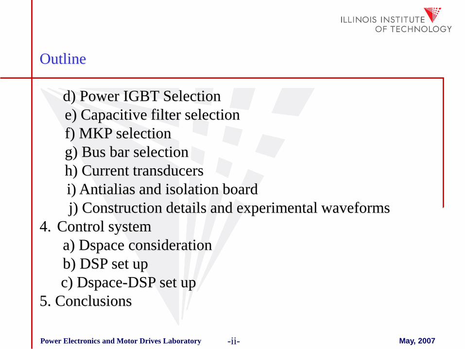
Outline
d) Power IGBT Selection
e) Capacitive filter selection
f) MKP selection
g) Bus bar selection
h) Current transducers
i) Antialias and isolation board
j) Construction details and experimental waveforms
4. Control system
a) Dspace consideration
b) DSP set up
c) Dspace-DSP set up
5. Conclusions
-ii- Power Electronics and Motor Drives Laboratory May, 2007
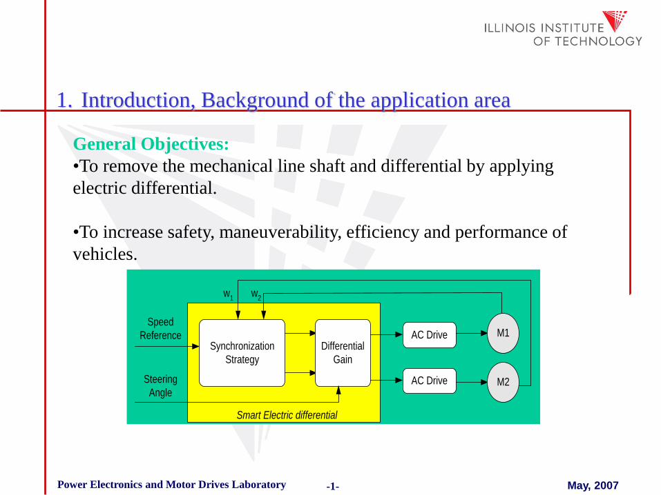
1. Introduction, Background of the application area
-1- Power Electronics and Motor Drives Laboratory May, 2007
Synchronization
Strategy
Speed
ReferenceDifferential
Gain
Steering
Angle
AC Drive
AC Drive
M1
M2
w1
w2
Smart Electric differential
General Objectives:
•To remove the mechanical line shaft and differential by applying
electric differential.
•To increase safety, maneuverability, efficiency and performance of
vehicles.
1. Introduction, Overall aims of this project
-2- Power Electronics and Motor Drives Laboratory May, 2007
Specific objectives:
• To devise and assess experimentally the DC-AC power electronic
converter techniques for electric differential power train.
• To develop a control system to manage the speed synchronization in
the wheels, ensuring an orderly flow of speed during both normal and
start-up conditions, ensuring that an adequate energy level is
maintained in the DC-AC power stage at all time.
• A DSP-based system and appropriate power hardware will be devised
and prototyped for demonstration and evaluation.

1. Introduction, General considerations of the Electric Power
stage
-3- Power Electronics and Motor Drives Laboratory May, 2007
Power
Electronic
Driver
Energy
Storage
System
Controller
Electric
Motor
Electric
Motor
Power
Electronic
Driver
The benchmark prototype is a three wheel vehicle,
with rear traction.

2. Electrical requirements of the electric power stage, Test
drive cycles
-4- Power Electronics and Motor Drives Laboratory May, 2007
The parameters considered to size the power electronic converter are:
CD= 0.5 (Open convertible)
Vb = 33.3 km/hr, 9.258 m/s. (Base speed of the vehicle)
Vf = 53.33 km/hr, 15 m/s .(Maximum speed of the vehicle)
g = 9.8 m/s2.
fr = 0.03
Pa = 1.202 kg/m3.
Af = 2 m.
Mv= 150 kg.
ta= 20 sec.
= 1.06438.
Vbase=1380 rpm. (Base speed of the motor).
Vmax=5000 rpm. (Maximum speed of the motor.
r= 0.2794m. (ratio of wheel)
N= 0.9 (Efficiency).
ig= 9.752900 (gear ratio), it was used ig=9 in the simulations.

2. Electrical requirements of the electric power stage, Test
drive cycles
-5- Power Electronics and Motor Drives Laboratory May, 2007
0
10
20
30
40
50
60
0 100 200 300 400 500 600 700 800
Time (s)
Velo
cit
y (
km
/hr)
-2,000
-1,000
0,000
1,000
2,000
3,000
4,000
5,000
6,000
7,000
8,000
9,000
10,000
0 100 200 300 400 500 600 700 800
Time (s)
Po
wer
(W
)

2. Electrical requirements of the electric power stage,
Summary of the baseline inverter
-6- Power Electronics and Motor Drives Laboratory May, 2007
Average power with last condition is 572.74 W, a maximum peak power of
6.095kW, and a minimum power of -824W.
For a two motor system instead of one single power system, the average
power system reflected in each motor& power drive will be equal to
286.30 W, a maximum peak power of 3 kW and a minimum power of -
424W (considering no losses

2. Electrical requirements of the electric power stage,
Summary of the baseline inverter
-7- Power Electronics and Motor Drives Laboratory May, 2007
t(seg)
Po
ten
cia
(kW
) 6.95 kW
125 117
Peak power consideration of each traction device must be oversized about
8 times the average power and not 5 times the rule of thumb for practical
applications .

-8- Power Electronics and Motor Drives Laboratory May, 2007
DMOC 445 from Solectria, (Azure) 38kW @ 312 V (continuous)
•CM400DU-12F 600V, 400 A IGBT, (240 kW)
•6.31times Overdesigned
•Driver M57160AL-01 from powerex.
•4 capacitor Chemicron in parallel, 1800µF
•PWM, Error and digital function implemented with PAL
•Relay Type S1730 - 2 POLE, Kraus and naimer.
•It does not use an encoder, kind of sensorless
2. Electrical requirements of the electric power stage,
Comparison with commercial traction inverter

3. Summary of the baseline inverter, Basic circuit description
and operation
-9- Power Electronics and Motor Drives Laboratory May, 2007
Z
Z Z
M2
A B
B
C
C
a
a´
b
b´
c
c´A
Z
Z Z
M1
7 pack-Inverter 1 7 pack-Inverter 2
Precharge
Over_voltage
protectionMain switch, relay
Overall electric diagram of the system Prototype.

3. Summary of the baseline inverter, Converter design
-10- Power Electronics and Motor Drives Laboratory May, 2007
3700.9171
220 3 220 3
P Wi A
6(0.9171 ) 5.82i A A
30007.874
220 3 220 3
P Wi A
Rated Current
Transient Current
Considering the maximum power demanded to each motor during the
driving cycle, we have:
Therefore the minimum current needed for one IGBT of each inverter is
at least 7.874A. Like a rule of thumb, it is given a 100% of tolerance for
safety reason. For that reason the minimum needed current in the IGBT
is equal to 16A

3. Summary of the baseline inverter, Component selection
-11- Power Electronics and Motor Drives Laboratory May, 2007
13
2 2
dcrms
VV
220 2 2 440 1.4312
1.7 1.163 1.16dcV Vdc
DC Bus Voltage
Considering the 220 Vrms line to line for the AC machine, and assuming a
space vector modulation to generate the PWM pattern, we have [1]:
Rearranging last eq, we have:
For a natural PWM, the needed dc bus voltage is Vdc=362V. It this
design, it is considered a Vdc=320V in the dc link bus, assuming that a
SPVPWM pattern will be used in the experimental set-up.

3. Summary of the baseline inverter, Power IGBT Selection
-12- Power Electronics and Motor Drives Laboratory May, 2007
Possible IGBT
Possible
IGBT
Main
Characteristics
Power Losses
per switch
W
Power Losses
per inverter
W
Thermal
Heatsink oC/W
Price
IRAMX20
UPC 60A
3-LEG
INTEGRATED
600V, 20A
20kHz
7,751128053
(8 KHz)
46,50676832 0,406146 $34.33
CPV364M
4U
3 LEG INTEGRATED
600V, 20A
8-60kHz
6,629992986
(10 KHz)
39,77995792 1,420526 $70.00
CPV364M
4F
3 LEG INTEGRATED
600V, 27A
8 kHz, max
6,639345945
(6 KHz)
39,83607567 1,402466 $70.00
IRG4PC40
KD
Single IGBT
600V, 25A
25kHz.
9,161164795
(6 KHz)
54,96698877 0,518296 $5.75
each,
$34.5
IRG4PC40
UD
Single IGBT
600V, 40A
8-60kHz.
9,206851863
(10 KHz)
55,24111118 0,472255 $10
each,
$60
PM50RLB
060
7-IGBT package
600V, 50A
10,71642367
(8 KHz)
64,29854203 0,959751 $142

3. Summary of the baseline inverter, Power IGBT Selection
-13- Power Electronics and Motor Drives Laboratory May, 2007
3. Summary of the baseline inverter, Capacitive filter
selection
-14- Power Electronics and Motor Drives Laboratory May, 2007
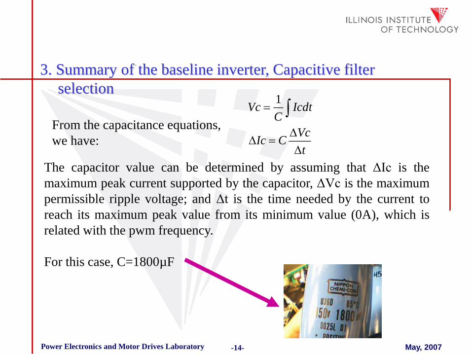
From the capacitance equations,
we have:
1Vc Icdt
C
VcIc C
t
The capacitor value can be determined by assuming that ΔIc is the
maximum peak current supported by the capacitor, ΔVc is the maximum
permissible ripple voltage; and Δt is the time needed by the current to
reach its maximum peak value from its minimum value (0A), which is
related with the pwm frequency.
For this case, C=1800µF

3. Summary of the baseline inverter, Bus bar selection
-15- Power Electronics and Motor Drives Laboratory May, 2007
Based on the design of the inverter, it was assumed that the 31A would flow
in the system continuously and that the bus bar rating needed to be higher
than this number.
The ampacity properties of various copper diameters were analyzed. Apart
from current rating, parameters such as insulation conductor material were
considered.
It was selected a copper bar of Thickness .050“,
recovered with kapton KPT-1 for insulation

3. Summary of the baseline inverter, Antialias and isolation
board
-16- Power Electronics and Motor Drives Laboratory May, 2007
The aconditioning board consists of the following sections:
1. 4 Isolation channels, ISO 122JP.
2. Anti aliasing filter, 2nd order, 1Khz cut off frequency.
3. 2 isolated dc supply +24 V input, ±15V output
4. Voltage shifter and jumper selection for dspace or dsp board.
• Dspace bipolar signal between -10 to 10V.
• DSP unipolar signal between 0V and 3V.

3. Summary of the baseline inverter, Antialias and isolation
board
-17- Power Electronics and Motor Drives Laboratory May, 2007 S
ou
rce
DC
/DC
15
V
So
urc
e D
C/D
C 1
5V
CONECTOR inversor
ISO122JP
74hc04
Input
Vdc
Input DC
current
ISO122JP
Input
IsaInput Isb
LM324
ISO122JP
ISO122JP
LM324
Input 24V
74hc04
So
urc
e +
5V
CONECTO
R inversor
CONECTO
R inversor
FINAL ORGANIZATION
For the PCB design were followed three basic rules, short lines, fat lines, and
a power plane in the upper side to avoid electromagnetic interference.

3. Summary of the baseline inverter, Antialias and isolation
board
-18- Power Electronics and Motor Drives Laboratory May, 2007
3. Summary of the baseline inverter, Construction details and
experimental waveforms
-19- Power Electronics and Motor Drives Laboratory May, 2007
Cables
Left motor
Heatsink
Cables
Right motor
Battery
Cables Cover made
of Aluminium
Chassis
IIT
Electric Differential
FJPP 2007 A. Emadi
Cover
Driver L
Driver R
Ant
ialia
s
R
Ant
ialia
s
L
Fuse
&Diode Conector
DSP
DSP
Bus Bar
Positive Top
Negative
Botom
Positive Negative
R
R
Internal organization

3. Summary of the baseline inverter, Construction details and
experimental waveforms
-20- Power Electronics and Motor Drives Laboratory May, 2007
Prototype Developed during the Fulbright grant.

4. Control System Dspace consideration
-21- Power Electronics and Motor Drives Laboratory May, 2007
Block diagram of the Indirect Field Oriented Control

4. Control System Dspace consideration
-22- Power Electronics and Motor Drives Laboratory May, 2007
Seniales de Torque
Error de Velocidad
ACKERMAN EMULATION
GAIN
speed rad/sec M2
speed rad/sec M1
speed RPM M2
speed RPM M1
isa8
Velocidad Referencia,
M1 y M2
[wm2]
Velocidad M2
[wm]
Velocidad M1
VLL-1
VDCLINK2
VAB1
Transport
Delay1
Transport
Delay
1
den(s)
Transfer Fcn7
1
den(s)
Transfer Fcn5
[te2]
Torque M2
Repeating
Sequence3
Repeating
Sequence
Product2
1
den(s)
Motor 2
-K- K2
In1
Out1
Out2
Out3
Out4
Indirect Control
FOC MOTOR 2
In1
Out1
Out2
Out3
Out4
Indirect Control
FOC MOTOR 1
I_vdclink
[TL1]
Goto9
[isc2]
Goto7
[isb2]
Goto6[isa2]
Goto5
[wref]
Goto4
[isc]
Goto2
[te1]
Goto11
[TL2]
Goto10
[isb]
Goto1[isa]
Goto
2
Gain9
-K-
Gain5
2
Gain4
-K-
Gain3
-K-
Gain2
-K-
Gain1
[TL2]
From9
[TL1]
From8
[wref]
From7
[wm]
From6
[wref]
From5
[wref]
From4
[wref]
From3
[wm2]
From2
[wm2]
From18
[wref]
From17
[teref]
From16
[te2]
From15
[te1]
From14
[wm2]
From13
[wref]
From12
[wm]
From11
[wref]
From1
In1
In2
In3
Out1
Ficticiuos Master
Pulse M1
TL1
Pulse M2
TL2
Seniales M1
Vab2
Seniales M2
Out5
Out2
Vab3
ETAPA DE POTENCIA
Corrientes M2
Corrientes M1
Block diagram of the Electric differential implemented in the Dspace environment.

4. Control System, DSP set up
-23- Power Electronics and Motor Drives Laboratory May, 2007
The eZdspTM F2812 has the following features:
• TMS320F2812 Digital Signal Processor
• 150 MIPS operating speed
• 18K words on-chip RAM
• 128K words on-chip Flash memory
• 64K words off-chip SRAM memory
• 30 MHz. clock
• 2 Expansion Connectors (analog, I/O)
• Onboard IEEE 1149.1 JTAG Controller
• 5-volt only operation with supplied AC adapter
• TI F28xx Code Composer Studio tools driver
• On board IEEE 1149.1 JTAG emulation connector

4. Control System, DSP set up
-24- Power Electronics and Motor Drives Laboratory May, 2007
To implement our software module control we used Code Composer
Studio v 3.1 which is a programming environment used to implement
various algorithms and load code onto a working with both “high” and
“low” level languages like C/C++ and Assembler.

4. Control System, DSP set up
-25- Power Electronics and Motor Drives Laboratory May, 2007
Due to time constrains, three control open loop
algorithm were implemented for only one IM
working directly to the USB port and JTAG
emulator.
The algorithms implemented were V/Hz, IFOC
and sensorless IFOC. All of them were based on
the note applications of TI ACI3_1, ACI3_2,
ACI3_4.
Note applications programs were modified to run
in the inverter developed at IIT.
Typical program flow diagram
implemented in the DSP.

4. Control System, Dspace-DSP set up
-26- Power Electronics and Motor Drives Laboratory May, 2007
Due to only 3 PWM channel are available in the dspace interface board, it
was not possible to run the Electric Differential with both IM.
In addition, due to lack of time for DSP programming, it was not possible
to run both IM and the electric differential controller with the DSP.
The final implementation of the electric differential will be implementing
the electric differential controller and one sensorless IFOC controller inside
the Dspace environment and using one DSP to control the second IM in
sensorless mode.

5. Conclusions and future work
-27- Power Electronics and Motor Drives Laboratory May, 2007
The following tasks are:
1. To program sensorless of the IM.
2. To validate the proposed electric differential algorithm.
A DC-AC power electronic converter has been designed for electric
differential application.
A DSP-based system and appropriate power hardware has been devised for
demonstration and evaluation.