Development of a FPGA based test system for Double Data ... · Universitµa degli Studi di Napoli...
92
Universit` a degli Studi di Napoli “Federico II” Facolt` a di Scienze MM.FF.NN. Tesi di dottorato di ricerca in Tecnologie Innovative per Materiali, Sensori ed Imaging XVII ciclo aggregato al XIX Development of a FPGA based test system for Double Data Rate high speed memory devices. Coordinatore: Candidato: Prof. Ruggero Vaglio Adele Di Cicco
Transcript of Development of a FPGA based test system for Double Data ... · Universitµa degli Studi di Napoli...

Universita degli Studi di Napoli“Federico II”
Facolta di Scienze MM.FF.NN.
Tesi di dottorato di ricerca in
Tecnologie Innovative per Materiali, Sensori ed Imaging
XVII ciclo aggregato al XIX
Development of a FPGA based test systemfor Double Data Rate high speed
memory devices.
Coordinatore: Candidato:Prof. Ruggero Vaglio Adele Di Cicco

ii

Contents
Introduction 1
1 High Data Rate Memory Devices 5
1.1 Introduction . . . . . . . . . . . . . . . . . . . . . . . . . . . . 5
1.2 Random Access Memory . . . . . . . . . . . . . . . . . . . . . 6
1.3 Synchronous DRAM . . . . . . . . . . . . . . . . . . . . . . . 10
1.4 DDR I SDRAM . . . . . . . . . . . . . . . . . . . . . . . . . . 10
1.5 DDR II SDRAM . . . . . . . . . . . . . . . . . . . . . . . . . 14
1.6 Functional Memory Testing . . . . . . . . . . . . . . . . . . . 19
1.6.1 Single-Cell Static Fault . . . . . . . . . . . . . . . . . . 20
1.6.2 Two-cell static faults . . . . . . . . . . . . . . . . . . . 22
1.7 March Test . . . . . . . . . . . . . . . . . . . . . . . . . . . . 23
1.8 Signal Integrity analysis for High Data Rate Memory . . . . . 24
2 Measuring Jitter in digital system 25
2.1 Introduction . . . . . . . . . . . . . . . . . . . . . . . . . . . . 25
2.2 Jitter Definition . . . . . . . . . . . . . . . . . . . . . . . . . . 26
2.3 Jitter Classification . . . . . . . . . . . . . . . . . . . . . . . . 26
2.4 Jitter Measurements . . . . . . . . . . . . . . . . . . . . . . . 29
2.5 Data Dependent Jitter (DDJ) . . . . . . . . . . . . . . . . . . 31
2.5.1 Duty Cycle Distortion . . . . . . . . . . . . . . . . . . 32
2.5.2 Inter Symbol Interference . . . . . . . . . . . . . . . . 33
2.6 Periodic Jitter . . . . . . . . . . . . . . . . . . . . . . . . . . . 34
2.7 Bounded Uncorrelated Jitter . . . . . . . . . . . . . . . . . . . 35
2.8 Total jitter . . . . . . . . . . . . . . . . . . . . . . . . . . . . . 37
iii

2.8.1 Calculating Total Jitter from Bathtub Curves . . . . . 39
2.8.2 The Dual-Dirac Model . . . . . . . . . . . . . . . . . . 41
3 The DDR II tester 45
3.1 Introduction . . . . . . . . . . . . . . . . . . . . . . . . . . . . 45
3.2 Board description . . . . . . . . . . . . . . . . . . . . . . . . . 50
3.3 FPGA description . . . . . . . . . . . . . . . . . . . . . . . . . 54
3.4 The functional tester . . . . . . . . . . . . . . . . . . . . . . . 55
3.4.1 March Element Decoder . . . . . . . . . . . . . . . . . 57
3.4.2 Command Sequencer . . . . . . . . . . . . . . . . . . . 59
3.4.3 The Data Path and Physical Layer Interface . . . . . . 62
3.4.4 The Read Data Compare Module . . . . . . . . . . . . 65
3.5 The Signal Integrity Analyzer . . . . . . . . . . . . . . . . . . 66
4 Experimental results 73
4.1 Introduction . . . . . . . . . . . . . . . . . . . . . . . . . . . . 73
4.2 Functional Tester Debug . . . . . . . . . . . . . . . . . . . . . 73
4.3 Signal Integrity Analyzer Debug . . . . . . . . . . . . . . . . . 78
Conclusions 85
Bibliography 87

Introduction
Semiconductor memories are widely considered to be one of the most impor-tant types of microelectronic components in modern digital systems [1]. It isreported that memories represent about 30% of the worldwide semiconduc-tor market [2]. The growing need for storage in computer, communications,consumer, and network applications is driving the continuous innovation ofvarious semiconductor memory technologies. Bigger and faster memories arealways desirable due to our insatiable appetites for voluminous transmissionand storage of data in these applications, i.e., the continuing technology in-novation is likely to increase the market share of commodity and embeddedmemories in the future. The Double Data Rate II (DDR II) SDRAM memory,which is the last generation of Dynamic Ram, is the most widely used typeof memory in the market today and its data rate is expected to move fromcurrently 400MHz to 667MHz and 800MHz in the near future. It is an ap-propriate memory solution for system ranging from workstations and serversto embedded communication system such as graphics, cache and main mem-ory for Personal Computer. The JEDEC (Joint Electron Device EngineeringCouncil)1 organization has helped the memory industry by creating memoryspecifications in the form of JEDEC standards. This standards cover physi-cal characteristics, electrical signal, register definitions, functional operations,memory protocol, etc. The exponential increase in the integration densityand complex manufacturing steps have made the memory more vulnerable tophysical defects than the other logic circuits. The fast development of mem-ory devices and the strong market competition have increased the standardsof these produced devices. The increased demand on reliability has, in turn,stressed the importance of memory testing technique. The chapter I startswith an overview of semiconductor memory devices, showing their evolution,and describing the improvements of each memory devices over its predecessor.
1JEDEC is a no-profit organization with members from memory, computer and testequipment manufacturers.
1

2
In this chapter is stressed the need to introduce an efficient testing process tosolve the problems related to the even increasing density. The traditional waysto test semiconductor memories, realized to detect physical defects related tothe high density are introduced. On the other hand, at the higher frequency,such as that of the DDR II, the signal integrity becomes an important issueto be considered for reliability of the memory operations. An introductionto the contribution to this problem of this Ph.D project is presented in thechapter I.
The chapter II describes in more details signal integrity issues related tohigh frequency systems such as high speed memory devices, starting from theJitter definition and the description of the major sources of jitter, through theclassification of the jitter, and ending with the method used to observe andstudy it.
The testing process is responsible for a large portion of the cost of thesememories, standing now at 40% and gradually rising with each new gener-ation. Companies usually develop the required memory tests in an ad hoc,relying heavily on an expensive combination of experience and statistics toconstruct the best test approach, the price of which is ultimately paid by theend consumer. Memory testing is expensive because of the high cost of thetest equipment (a production memory tester costs more than 500.000 Dollars),a cost that has to be distributed over all the produced chips. However theequipments available on the market are not able to perform both functionaltests and signal integrity analysis. The study of the signal integrity, furtherincreases the production time and costs. In this thesis project, a new alterna-tive approach to the development of an industrial memory testing is proposed.It is more systematic and less expensive than the currently prevalent test ap-proaches. The new approach makes it possible to enhance memory tests inmany different manufacturing stages, starting from the initial test applica-tion stage where silicon is manufactured, and ending the memory ramp-upstage where products are shipped to the customer. The tester realized re-duce the test time and costs being based on the use of a last generation FieldProgrammable Gate Arrays (FPGA), which implements 90% of the neededfunctionalities. Chapter III deals with the description of the overall charac-teristic of the realized tester, whose design, production and testing representthe innovative issues of this Ph.D project. The realized tester, is able toperform:
• the functional test allowing the fast detection of physical defects,
• the signal integrity analysis, implementing on each memory channel, the

3
function of a sampling oscilloscope. The advantage of this feature is tobe able to perform complex analysis without the use of an external andexpensive equipment. The complex analysis include the eye diagramopening, rise and fall time, setup and hold time measurements,
• the parametric test which is aimed at the validation of electrical param-eters (leakage currents, voltage level, rise and fall time, etc.) accordingto the specifications.
Chapter IV deals with the description of the debug of the functional testerand the debug of the signal integrity analyzer. The functional tester capa-bility to detect physical defects has been verified comparing the test resultswith those obtained the traditional equipment. The signal integrity analyzerperformances have been evaluated comparing the eye diagrams (rising edge,falling edge, eye opening, etc.) obtained with the customized-tester with thoseobtained by the use of last generation high bandwidth oscilloscope.

4

Chapter 1
High Data Rate Memory
Devices
1.1 Introduction
Technical advancements such as high-speed processors, multimedia applica-tion with high resolution moving pictures, and serial data links with Gb/s datarates are driving the need for higher bandwidth memory system. The grow-ing need for storage in computer, communications, consumers and networkapplications is the driving force in the advancements of DRAM technology.Mainstream DRAMs have evolved over the years through several technol-ogy enhancements such as SDRAM (Synchronous Dynamic Random AccessMemory), DDR (Double Data Rate) SDRAM, DDR II (Double Data Rate II)SDRAM, DDR III (Double Data Rate III) SDRAM. Fig.1.1 shows the datatransfer rate and DRAM architecture trends of main memory for server andhigh-end PC. Currently, Double Data Rate II is dominating the market formain memory and its data rate is expected to move from currently 400MHzto 667MHz and 800MHz in the near future.
The exponential increase in the integration density and the complex man-ufacturing steps have made the memory more vulnerable to physical defectsthan other logic circuits. This attitude have made memory testing a signif-icantly important task to perform. Due to the increasing complexity of thememory chips, their testing is quickly becoming a difficult issue, which repre-sent the real bottleneck of the entire production process.
5

6 Chapter 1. High Data Rate Memory Devices
Figure 1.1: Data transfer rate and DRAM architecture trends of high-end PC andservers.
This chapter describes the traditional ways to test semiconductor memo-ries, realized to detect physical defects and anomaly in functional behavior.
At the higher frequency, such as that of DDR II, signal integrity becomesan important issue for reliable memory operation. In this chapter there is anintroduction to the work done in this thesis, which is aimed at the analysisof the signal integrity with faster, lower cost and more compact solution thanthe testing environments today available on the market.
1.2 Random Access Memory
The name RAM stands for a memory device in which cells may be accessedat random to perform a read or a write operation. Depending on the internalarchitecture and the actual memory cell structure, RAMs may be divided into:
• dynamic RAMs (DRAMs),
• static RAMs (SRAMs).
A simple block diagram of a RAM is given in fig.1.2. Three main inputare shown: a read/write (R/W) switch to discriminate the type of operation

1.2. Random Access Memory 7
Figure 1.2: Block diagrams of a RAM .
Figure 1.3: Electrical structure of (a) SRAM and (b) DRAM core cells.
performed, an address input which identifies the cell to be accessed and a datainput bus that supplies the data to be written in case of write operation. ARAM also has a data output bus to be used on a read operation to forwarddata from the addressed cell to the outside world. In principle, both DRAMsa SRAMs share this same general interface, but the specific implementationis different and mainly depends on the targeted application of the memory.
A typical structure of an SRAM cell is shown in fig.1.3(a). The cell isconstructed using six transistors, four of which are of one transistor type(NMOS) while the other two are of another type (PMOS). The word line(WL) performs the address selection function for the cell. The true bit line(BT) and complement bit line (BC) serve both as the data input line andthe data output line for the cell at the same time. The selection between

8 Chapter 1. High Data Rate Memory Devices
performing a read or a write operation is fulfilled by other memory partsexternal to the cell. The operation of the cell is based on the fact that SRAMcells are bistable electrical elements (i.e., circuits that have two stable states).Each state is used to represent a given logical level. Once a cell is forced intoone of the two states, it will stay in it as long as the memory is connected tothe power supply; the name ”static RAM” refers to this property.
The electrical structure of a DRAM cell is shown in fig.1.3(b). The cellis constructed using one transistor and one capacitor. The WL performs theaddress selection, while the bit line (BLs) are used as both the data inputand data output lines. The selection between read and write operations isperformed by other parts of the memory. The DRAMs are constructed ofsimple capacitive elements that store electrical charges to represents a givenlogical level. Inherently, DRAM cells suffer from gradual charge loss, as aresult of phenomenon known as transistor leakage currents, which causes acell to lose its charge gradually. In order to help cells keep their state, itis necessary for DRAMs to rewrite, or refresh, the already stored data bitsfrom time to time before the cells lose their charge completely. The ”dynamicRAM” refers to the fact that the data stored in the DRAM cell may changespontaneously after a given period of time.
Both DRAMs and SRAMs are called volatile memories because they canonly keep their data content if they stay connected to the power supply. Acloser look at the two RAM structures reveals that SRAMs store their data ac-tively by pulling their nodes to high or low voltage levels, while DRAMs storetheir data in capacitive elements that take time to charge up and discharge.Therefore, SRAMs have a much higher performance than DRAMs, and thisis the reason they are used as the first level memory (or cache memory) di-rectly supporting the central processing unit (CPU) in a microprocessor. Themain advantage that DRAMs have over SRAMs is in their density. Fig.1.3clearly shows that DRAM cells are simple, compact elements that achievemuch higher chip densities than their SRAM counterparts, which also makesthem much cheaper. This cost difference is so important that it outweighs allother aspects in most applications.
DRAMs core architecture consists of memory cells organized into a two-dimensional array of row and columns (fig.1.4).The address bus is multiplexedbetween row and column components. The multiplexed address bus uses twocontrol signals -the row and column address strobe signals, RAS and CAS,respectively- which cause the DRAM to latch the address components. Ad-ditional DRAM control signals include WE (Write enable) for selecting write

1.2. Random Access Memory 9
Figure 1.4: Conventional DRAM block diagram.
or read operation, CS for selecting the DRAM, and OE (Output Enable).The row address causes a complete row in the memory array to propagatedown the bit lines to sense amps. The column address selects the appropriatedata subset from the sense amps and causes it to be driven to the output pins.DRAM reads are destructive, meaning the data in the row of memory cells aredestroyed in the read operation. Therefore, the row data need to be writtenback into the same row after the completion of a read or write operation on arow. This operation is called Precharge and is the last operation on a row. Itmust be done before accessing a new row and is referred to as closing an openrow. A DRAM row is called a memory page and once the row is opened itis possible to access multiple sequential or different column addresses in therow. This increases memory access speed and reduces memory latency by nothaving to resend the row address to the DRAM when accessing memory cellsin the same memory page.

10 Chapter 1. High Data Rate Memory Devices
The early DRAMs read cycle had four step. First, RAS goes low witha row address on the address bus. Secondly, CAS goes low with a columnaddress on the address bus. Third , OE goes low and read data appearson the data bus. The time from the first step to the third step when thedata is available on data bus is called latency. The last step is RAS, CAS,OE going high (inactive) and waiting for the internal precharge operation tocomplete restoration of the row data after the destructive read. Signal timingof the above signals is related to the edges and is asynchronous. There is nosynchronous clock operation.
1.3 Synchronous DRAM
In the Synchronous DRAM the memory operations are synchronized withthe functionality of the system by using a single system clock. The typeof memory command is determined by the state of the control signal at therising edge of the SDRAM clock. The clock is used to drive an internal finitestate machine that pipelines incoming commands. This allows the chip tohave a more complex pattern of operation than DRAM, which does not havesynchronizing control circuits. Pipelining means that the chip can accepts anew command before it has finished processing the previous one. In pipelinedwrite, the write command can be immediately followed by another commandwithout waiting for the data to be written to the memory array. In a pipelinedread, the requested data appears a fixed number of clock pulses after the readcommand. It is no necessary to wait for the data to appear before the nextcommand. This delay is called the latency, and is an important parameterwhich will be described in the following paragraph.
1.4 DDR I SDRAM
The next stage of evolutionary migration from standard DRAMs is DDRI (Double Data Rate I) SDRAM which dramatically increases DRAM busspeed by activating data output on both the rising and falling edges (doublepumped) of the system clock rather than on just the rising edge.

1.4. DDR I SDRAM 11
Figure 1.5: Functional block diagram with SDR and DDR interface.

12 Chapter 1. High Data Rate Memory Devices
Figure 1.6: Simplified block diagram of 2n-prefetch read.
The main functional differences between DDR and Single Data Rate (SDR)are:
• the double data rate/2n-prefetch architecture designed to transfer twodata words per clock cycle at I/O pins.
• the strobe based data bus to provide high speed signal integrity.
• Stub Series Terminated Logic 2 interface with differential inputs andclocks.
Fig.1.5 shows the difference between a DDR I and SDR (Single Data Rate)SDRAM functional block [3] . It reveals that the memory core is essentiallythe same. Both have an identical addressing and command control interface,a four-bank memory array (to provide multiple interleaved memory access)and both incorporate the same refresh requirements. The double data ratememory utilizes a differential pair for the system clock and therefore will haveboth a true and complementary clock signals. The main differences are foundin the data interface.
First, DDR adds phase-lock-loop circuitry to existing SDRAM designs.PLL technology enables tighter synchronization of data output to the device’sclock, which eliminates wasted clock cycles, makes the process more efficient,and improves performance.
The SDR data interface is a fully synchronous design where the data is onlycaptured on the positive clock edge. The internal bus is the same width as the

1.4. DDR I SDRAM 13
Figure 1.7: Simplified block diagram of 2n-prefetch write.
external data bus and the data latches into the internal memory sequentiallyas it passes through the I/O buffers.
The DDR I memory data is a true synchronous design, where the data iscaptured twice per clock cycle with a bidirectional data strobe. This architec-ture employs a 2n prefetch architecture, where the internal data bus is twicethe width of the external bus. This allows the internal memory cell to passdata to I/O buffer pairs.
Fig.1.6 show a simplified block diagram of 2n-prefetch READ. For eachsingle read access cycle internal to the device, two external data words areprovided. Similarly, two external data words written to the device are inter-nally combined and written in one internal access (as shown in fig.1.7). TheDDR command bus consist of a clock enable, chip select, row and columnaddresses, bank address and write enable. Commands are entered on the pos-itive edges of clock and data occurs on both positive and negative edges ofthe clock.
In a SDR system, data output are referenced to a common, free-runningsystem clock. Instead, the DDR memory bus has one clock for the controlsignals and 18 strobes for the data groups. The data strobes are non-free-running signal driven by the device which is driving the data signals (thecontroller for WRITEs, the DRAMs for READs). At the DRAM device level,for READs, the data strobe (DQS) signal are effectively additional data output(DQ) with a predetermined pattern; for WRITEs, the strobe signals are used

14 Chapter 1. High Data Rate Memory Devices
as clocks to capture the corresponding input data. At the board level, thestrobe signals have identical loading to data signals and should be routedsimilarly.
For READs, the data strobe signals are edge-aligned with the data signals,meaning that all data and data strobes are clocked out of the device by thesame internal clock signal, and all will be presented at the outputs at nominallythe same time. The controller will internally delay the received strobe to thecenter of the received data eye.
For WRITEs, the controller must provide the data strobes center-alignedrelative to data. That is, strobe transitions occur nominally 90 degrees (rela-tive to the clock frequency) out of phase with data transitions.
READs and WRITEs use a different alignment in order to avoid replicatingthe delay circuitry throughout the DRAM.
Previous SDR memory technology used LVTTL and a fixed voltage levelfor signal interface. DDR I SDRAM utilizes differential inputs as a referencevoltage for all interface signals. This interface is called SSTL2, which standfor stub series terminated logic for 2.5volts. SSTL2 is an industry standarddefined by JEDEC document. Although some DRAMs will support a reduceddrive output, most will comply with the SSTL2 Class II drive levels.
Benefits to the SSTL2 interface include symmetrical low and high levels,improved signal integrity, and better noise immunity, as the input levels trackminor variations in the supply voltage.
1.5 DDR II SDRAM
In order to avoid the problem associated with increased data rate, JEDEChas standardized DDR-II SDRAM, targeting 800Mb/s at much lower supplyvoltage than DDR-SDRAM. DDR-II is specified to operate with 1.8V supplyvoltage while DDR SDRAM use 2.5V supply voltage. This voltage scalingenhancement has the potential to reduce overall power requirements for thememory system. Another benefit of the lower operating voltages is the lowerlogic voltage swings. For the same slew rate, the reduced voltage swingsincrease logic transition speeds to support faster clock rates. In addition, thedata strobe can be programmed to be a differential signal. Using differentialdata strobe signal reduces noise, crosstalk, dynamic power consumption andEMI (Electromagnet Interference) and increases noise margin.

1.5. DDR II SDRAM 15
Figure 1.8: DDR II block diagram.

16 Chapter 1. High Data Rate Memory Devices
Figure 1.9: Two slot memory system with SSTL bus terminated by ODT.
The channel structure of a DDR-II SDRAM (fig.1.8) memory system isbasically the same as that of a DDR-I SDRAM memory system [4].
DDR II improves data bandwidth by using eight banks. The eight banksincrease the flexibility of accessing large memory DDR II by interleaving differ-ent memory bank operations. The DDR II architecture employs 4-bit prefetcharchitecture, i.e. the internal bus width has been made four times wider thanthe external bus width, so that data bus transfers can be accelerated by afactor of four without having to change the operating speed of the internalbus (memory cell array).
The On-Die Termination is the most significant feature that has beenadded to the DDR II SDRAM. This function greatly improve the signal in-tegrity at over 533Mb/s operation. Unlike the conventional SSTL bus of DDRSDRAM, termination resistors are located inside the DRAMs in the DDR-IImemory system as shown in fig.1.9, and they can be switched ON and OFF.Embedding the termination resistors inside the DRAM, the DDR-II memorysystem has much better signal integrity than conventional SSTL bus. In theusual way, i.e. with motherboard termination, a resistor with a suitable re-sistance value is connected at the end of transmission path (fig.1.10). Thismethod doesn’t reduce signal reflection adequately in the operating range usedby DDR II SDRAM. In fact, if there are several DRAMs on the same bus,such as is shown in fig.1.10, DRAM that are in active mode are affected byreflected signal from DRAM that are in stand by mode. In other words, re-flections caused at the I/O interface to the memory chips will have to re-enterthe bus first before they can be terminated. There is a constant noise level on

1.5. DDR II SDRAM 17
Figure 1.10: Signal Reflection when Using Motherboard Termination.
Figure 1.11: ODT and Reflected Signals.
the bus that will interfere with the data signals and cause quality degrada-tion. Using ODT, all chips that are not selected for data I/O, that is, thosethat are in standby mode will have ODT switched On to eliminate reflectionwhere it originates, that is, at the bus to die interface. As a result, there isno possibility for the reflections to reenter the bus and contaminate the othersignals (fig.1.11).
Tab.1.1 [5] compares the simulated signal integrity between the conven-tional motherboard terminated (MBT) bus and ODT bus of DDR-II SDRAM.The inter-symbol interference (ISI), aperture size, and slew rate are all betterin the ODT bus than in MBT bus. The ODT can have either 50Ω, 75Ω or150Ω depending on the system configuration.

18 Chapter 1. High Data Rate Memory Devices
Write Read
MBT ODT MBT ODT
Inter-symbol interference [ps] 493 432 503 373
Aperture [V] 0.43 0.85 0.67 1.14
Slew [V/ns] 0.42 0.62 0.59 0.88
Table 1.1: Signal Integrity Comparison.
Another function that has been added to the DDR II is the Off-Chip Driver[6]. As just discussed above, DDR II introduce a bidirectional, differential I/Odata strobe consisting of DQS and DQS as complementary signals. Differ-ential means that the two signals are measured against each other instead ofusing a simple strobe signal and a reference point. In theory the pull-up andpull-down signals should be mirror-symmetric to each other but reality showsotherwise. That means that there will be skew-induced delays to reaching theoutput high and low voltages (VOH and VOL) and the cross points betweenDQS and DQS used for clock forwarding will not necessarily coincide withthe DQ crossing the reference voltage (Vref) or even be consistent from oneclock to the next. The mismatch between clock and data reference points isreferred to as the DQ-DQS skew. One way to solve the problem is to useOff-Chip Driver calibration where both parts of the differential strobes arecalibrated against each other and against the DQ signal. Through this sort ofcalibration, the ramping voltages are optimized for the buffer impedances toreduce over and undershooting at the rising and falling edges. More impor-tantly, DQS and DQS are matched so that their cross point coincides withthe DQ signal crossing the reference voltage to eliminate DQ-DQS skew. Insummary, the entire scheme results in better compatibility between differentdesigns, higher signal integrity through minimization of DQ-DQS skew andreduced overshoot/undershoot for better signal quality.
Another feature is that signal reflections can be controlled through se-lectable output drive levels. Two mode are selectable, full and reduced drive.DDR II configured as full drive has a target output impedance of approxi-mately 18Ω. When the device is configured as reduced drive the target outputimpedance is approximately 40Ω.

1.6. Functional Memory Testing 19
Figure 1.12: a)Before OCD calibration; b)After OCD calibration.
1.6 Functional Memory Testing
The fast development of memory devices and the strong market competitionhave increased the standards of these produced devices. The increased de-mand on reliability has, in turn, stressed the importance of failure analysisand memory testing techniques. Tests for semiconductors’ memories have ex-perienced a long development process. Before 1980, tests required long testtimes for a given fault coverage (FC) (i.e. the number of detected faults di-vided by the number of total faults), typically of order O(n2), where , n isthe size of the memory. In order to reduce the test time and improve the FC,during the early 1980s, the Functional Faults Models, which are abstract faultmodels, were introduced. A functional fault model is defined as the deviationof the observed memory behavior from the functionally specified one, undera given sequence of performed memory operation. The advantages of thesemodels was that the FC could be proven while the test time was usually oforder O(n), that is linear with the size of the memory. The first functionalmodel were not based on real memory design. The next stage was the intro-duction of the inductive fault analysis (IFA). IFA is a systematic procedureto predict the faults in an integrated circuit by injecting spot defects in thesimulated geometrical representation of the circuit. The result was that newfunctional fault models where introduced. In the late 1990s, the experimentalresults of applying a large number of tests to a large number of chips indicatedthat many functional tests detect faults which cannot be explained with theexisting fault models at that time. This led to the introduction of the frame-work of all possible fault models for memories based on the fault primitive(FP)

20 Chapter 1. High Data Rate Memory Devices
concept. Any difference between the observed and expected memory behaviorcan be denoted by the following notation < S/F/R >, referred to as a faultprimitive(FP). S describes the operation sequence that sensitizes the fault, Fdescribes the value of the faulty cell and R describes the logic output level ofa read operation. For example, in the FP < 0cw1c/0/− >, S = 0cw1c meansthat cell c is assumed to have the initial value 0, after which a 1 is written intoc. The fault effect F=0 indicates that after performing a w1 to c, as indicatesby S, c remains in state 0.The concept of FP also allowed for the classificationof the memory faults framework in different classes:static against dynamic(depending on the number of operation required to sensitize the the fault),simple against linked (depending on the way the FPs manifest themselves)and so on. The faults can be classified into different class depending on S. Ifonly a single cell is involved in S the fault is called single cell fault, if more cellsare involved in S the FP sensitized by the corresponding S is called couplingfault. In the coupling fault a cell or group of cells (aggressor) influences thebehavior of another cell (victim).
1.6.1 Single-Cell Static Fault
Single cell faults are restricted to a single cell of the memory array. This classconsists of the following fault types:
1. State Fault (SFx)— A cell is said to have a State Fault if the logic valueof the cell changes before it is accessed (read or written), even if nooperation is performed on it. No operation is needed to sensitize it and,therefore , it only depends on the initial stored value in the cell. Thereare two types of state faults: State-0 fault (SF0) and State-1 fault (SF1).
• State-0-fault (SF0) =< 0/1/− >,• State-1-fault (SF1) =< 1/0/− >
2. Transition Fault (TFx)— A cell is said to have a transition fault if it failsto undergo a transition (0 → 1 or 1 → 0) when it is written. This faultis sensitized by a write operation and depends on both the initial storedlogic level and the type of the write operation. There are two types oftransition faults: Up transition fault (TF1) and Down transition fault(TF0)

1.6. Functional Memory Testing 21
• Down transition fault (TF0) =< 1w0/1/− >,• Up transition fault (TF1) =< 0w1/1/− >
3. Read Destructive Fault (RDFx)— A cell is said to have a read destructivefault if a read operation performed on the cell changes the data in thecell and returns an incorrect value on the output. There are two typesof read destructive faults: Read-0 destructive fault (RDF0), Read-1destructive fault (RDF1).
• Read-0 destructive fault (RDF0) =< 0r0/1/1 >,• Read-1 destructive fault (RDF1) =< 1r1/0/0 >
4. Write Destructive Fault (WDFx)— A cell is said to have a destruc-tive fault if a non-transition write operation causes a transition in thecell.There are two types of write destructive faults: Write-0 destructivefault (WDF0) and Write-1 destructive fault (WDF1).
• Write-0 destructive fault (WDF0) =< 0w0/1/− >,• Write-1 destructive fault (WDF1) =< 1w1/0/− >
5. Incorrect Read Fault (IRFx)— A cell is said to have an incorrect readfault if a read operation performed on the cell returns the incorrect logicvalue, while keeping the correct stored value in the cell. There are twotypes of incorrect read faults:Incorrect read-0 fault (IRF0) and Incorrectread-1 fault (IRF1).
• Incorrect read-0 fault (IRF0) =< 0r0/0/1 >,• Incorrect read-1 fault (IRF1) =< 1r1/1/0 >
6. Deceptive Read Destructive Fault (DRDFx)— A cell is said to have adeceptive read destructive fault if a read operation performed on thecell return the correct logic value, while changing the contents of thecell. There are two types of deceptive read disturb faults: Deceptive r0destructive fault (DRDF0) and Deceptive r1 destructive fault (DRDF1).
• Deceptive r0 destructive fault (DRDF0) =< 0r0/1/0 >,• Deceptive r1 destructive fault (DRDF1) =< 1r1/0/1 >

22 Chapter 1. High Data Rate Memory Devices
1.6.2 Two-cell static faults
In the coupling fault a cell or group of cells (aggressor) influences the behaviorof another cell (victim). This class consists of the following fault types:
1. State coupling fault (CFst)— Two cells are said to have a state couplingfault if the victim is forced into a given logic state only if the aggressoris in a given state, without performing any operation on the victim.
2. Disturb coupling fault (CFds)— Two cells are said to have a disturbcoupling fault if an operation (write or read) performed on the aggressorforces the victim into a given logic state. Here, any operation performedon the aggressor is accepted as a sensitizing operation for the fault, beit a read, a transition write or a non-transition write operation.
3. Transition coupling fault (CFtr)— Two cells are said to have a tran-sition coupling fault if the state of the aggressor results in the failureof a transition write operation performed on the victim. This fault issensitized by a write operation on the victim, while the aggressor is ina given state.
4. Write destructive coupling fault (CFwd)— A cell is said to have a writedestructive coupling fault if a non-transition write operation performedon the victim results in a transition, while the aggressor is in a givenlogic state.
5. Read destructive coupling fault (CFrd)—Two cells are said to have a readdestructive coupling fault if a read operation performed on the victimdestroys the data stored in the victim, while a given state is present inthe aggressor.
6. Incorrect read coupling fault (CFir)— Two cells are said to have anincorrect read coupling fault if a read operation performed on the victimreturns the incorrect logic value, while the aggressor is in a given state.
7. Deceptive read destructive coupling fault (CFdr)—A cell is said to havea deceptive read destructive coupling fault if a read operation performedon the victim returns the correct logic value and changes the contentsof the victim, while the aggressor is in a given logic state.

1.7. March Test 23
1.7 March Test
In order to inspect memory devices for possible faulty behavior, memory test-ing is performed on all produced memory components. Many types of memorytests are being used today, each with its own advantages and disadvantages.March tests are among the most popular memory tests, due to their low com-plexity and high fault coverage.
A March test consists of a sequence of march elements; a march elementconsists of a sequence of operations which are all applied to a given cell,before proceeding to the next cell. The way one proceeds to the next cellis determined by the address order which can be an increasing address order(denoted by ⇑), or a decreasing address order (denoted by ⇓). For some marchelements the address order can be chosen arbitrarily, this will be indicated bythe m symbol. An operation, applied to a cell, can be a w0 (write ’0’), a w1(write ’1’), a r0 (read ’0’), or a r1 (read ’1’) operation. A complete marchtest is delimited by the ’...’ bracket pair, while a march element is delimitedby ’(...)’ bracket pair. In the following the most used march test are listed:
MATS: m (w0);⇑ (r0, w1);m (r1)MATS+: m (w0);⇑ (r0, w1);⇓ (r1, w0)
MATS++: m (w0);⇑ (r0, w1);⇓ (r1, w0, r0)
March X: m (w0);⇑ (r0, w1);⇓ (r1, w0);m (r0)March Y: m (w0);⇑ (r0, w1, r1);⇓ (r1, w0, r0);m (r0)
March C: m (w0);⇑ (r0, w1);⇑ (r1, w0);m (r0) ⇓ (r0, w1);⇓ (r1, w0);m(r0);
March C-: m (w0);⇑ (r0, w1);⇑ (r1, w0);⇓ (r0, w1);⇓ (r1, w0);m (r0); MOVI: ⇓ (w0);⇑ (r0, w1, r1);⇑ (r1, w0, r0);⇓ (r0, w1, r1);⇓ (r1, w0, r0);
IFA-9: m (w0);⇑ (r0, w1);⇑ (r1, w0);⇓ (r0, w1);⇓ (r1, w0); Delay;m (r0, w1); Delay;m(r1);
IFA-13: m (w0);⇑ (r0, w1, r1);⇑ (r1, w0, r0);⇓ (r0, w1, r1);⇓ (r1, w0, r0); Delay;m(r0, w1); Delay;m (r1);

24 Chapter 1. High Data Rate Memory Devices
1.8 Signal Integrity analysis for High Data Rate
Memory
The data rate of the DDR II is expected to move from currently 400MHz to667Mhz and 800MHz in the near future. Faster clock speeds requires smallervoltage swings and shorter setup and hold time. As result, data valid win-dow means that jitter induces noise, cross talk, and intersymbol-Interferencefurther reduce its size, creating errors. The signal integrity analysis is stilla challenging task, that could not be studied with traditional tools cited inprevious paragraph. The easiest way to study signal integrity is to plot theeye diagrams using an ultrawideband sequential oscilloscope.
This thesis work provides a memory test system which performs the tradi-tional tests in order to detect functional faults and supports up to 64 channelssimultaneous signal integrity testing.
The memory test is designed to provide, on each memory channel, thefunctions of a sampling oscilloscope. For each channel performs eye diagramanalysis, rise/fall time, logic level and eye opening measurements.

Chapter 2
Measuring Jitter in digital
system
2.1 Introduction
The obvious technology trend today is to have for-ever increasing bit rates,higher clock speeds and technology advances that keep lowering operatingvoltages, reducing package sizes and ball pitch, and forcing more componentsinto a smaller amount of board area. As frequency increases, the trace ona circuit board become more than simple conductors. At lower frequencies(such as the clock rate of an older digital system) the trace exhibits mostlyresistive characteristics. At higher frequencies, the trace begins to act likean impedance not purely resistive. A the highest frequencies, the trace’sinductance plays a larger role. All of this characteristics can adversely affectthe integrity of the transmitted signals.
A signal integrity problem is defined as any phenomenon that can com-promise a signal’s ability to convey binary information. Having good signalintegrity means controlling unwanted noise on logic signals. Noise falls intoone of two main domains:
• Level related noise affects the logic level of the signal. If the noise islarge enough, the signal may cross the threshold from a desired logicstate to undesired state and propagate into other logic.
• Time related noise, affect the position of a signal transition and causes
25

26 Chapter 2. Measuring Jitter in digital system
setup/hold window for data sampling to be violated, thereby allowingincorrect data to be sampled and propagated through the system.
The combination of amplitude and timing jitters contribute to reduce sig-nal margins in both the time and frequency domains, effectively reducing thewindow in which good data is available.
2.2 Jitter Definition
Jitter is usually defined as the deviation of a timing event of a signal from itsideal position [7]. Jitter describes a timing uncertainty, and therefore has tobe considered when we look a timing budget of a design. Jitter is just anothercomponent that makes part of the bit period unusable for sampling just likesetup and hold time. However unlike setup and hold times that are usuallythoroughly specified for logic families and can be taken from data sheets, jitteris a function of the design and has to be measured. There are two definitionsof jitter, an analog and a digital one. In the analog world jitter is also knownas phase noise, and defined as a phase offset that continually changes thetiming of a signal
S(t) = P (t + Φ(t)) (2.1)
where S(t) is the jittered signal waveform, P(t) is the undistorted waveform,and φ(t) is the phase offset, or phase noise. This definition is most usefulin the analysis of analog waveform like clock signals, and frequently used toexpress the quality of oscillators. In the digital world, we are looking only atthe 1-0 and 0-1 transitions of the signal, and jitter is therefore only definedwhen such a transition occurs (crossover). The jittered digital signal can bewritten as
tn = Tn + Φn (2.2)
where tn is the time when the nth transition occurred, Tn is the ideal timingvalue for the nth transition, and Φn is the time offset of this transition (advanceor delay), also known as the time jitter.
2.3 Jitter Classification
Jitter on a signal will have different characteristics depending on its causes,so categorizing the sources of jitter becomes important for measuring and

2.3. Jitter Classification 27
analyzing jitter [8].
The random noise mechanisms fall in the first category, processes thatrandomly introduce noise to a system. These sources include:
• Thermal Noise which can be represented by broadband ”white” noise,and has flat spectral density. It is generated by the transfer of energybetween ”free” electrons and ions in a conductor. The amount of energytransfer and, therefore, the amount of noise, are related to tempera-ture. It is associated with electron flow in conductors and increaseswith bandwidth, temperature and noise resistance.
• Shot Noise is broadband ”white” noise generated when electrons andholes move in a semiconductor. Shot noise amplitude is a function ofaverage current flow. The current fluctuations about the average valuegive rise to noise.
• Flicker Noise has a spectral distribution that is proportional to 1/fα
where α is generally close to unity. Because flicker noise is proportionalto 1/f , its contribution is most dominant at lower frequencies. Theorigin of flicker noise is a surface effect due to fluctuations in the car-rier density as electrons are randomly captured and emitted from oxideinterface traps.
The second category is ruled by system mechanisms, effects on a signal thatresult from characteristics of its digital system. Examples of system relatednoise sources include:
• Crosstalk which occurs when the magnetic or electric fields of a signalon a conductor are inadvertently coupled to an adjacent signal-carryingconductor. The coupled signal components algebraically add to thedesired signal, and can slightly alter its bias depending on the amount ofcoupling and the frequency content of the interfering signal. The alteredbias translates into jitter as the signal crosses the receiver’s threshold.
• Electromagnetic Interference or EMI which is the result of unwanted ra-diated or conducted emissions from a local device or system. Switching-type power supplies are common sources of EMI. These devices canradiate strong, high frequency electric and magnetic fields, and theycan conduct a large amount of electrical noise into a system if they lackadequate shielding and output filtering.

28 Chapter 2. Measuring Jitter in digital system
• Reflections which occur when impedance mismatches are present in adata channel. With copper technology, the max power transfer oc-curs when the transmitter and receiver have the same characteristicimpedance as the medium. If an impedance mismatch is present at thereceiver a portion of the energy is reflected through the medium to thetransmitter. Reflections typically come from uncontrolled stubbing andincorrect terminations. Reflected energy, or energy not available to thereceiver, reduces the signal to noise ratio at the receiver and increasejitter. If the transmitter is also mismatched, the transmitter absorbsa portion of the reflected signal energy while the remainder is reflectedtoward the receiver.
The so-called data category includes Data dependent mechanisms, in whichthe patterns or other characteristics of the data being transferred affect thenet jitter seen at the receiver. Data-dependent jitter sources include:
• Duty Cycle Distortion which occurs when long strings of ones or zeroscause the voltage level to drift and consequently delay the edge transi-tion. It is observed when the durations of logic 1 pulses are differentthan the duration of logic 0 pulses. More details will be shown in thepar.2.5.1.
• Intersymbol Interference (ISI) which is caused by attenuation and band-width limitations of transmission structure. It is a function of the datarate, board layout and material, and the data pattern sent over the link.The ISI results in reduced edge speeds, and in both retarded or advancededges relative to their ideal positions. More details on ISI will be shownin the par.2.5.2
The mentioned sources of jitter are categorized into two types, unboundedand bounded. Unbounded jitter does not achieve a maximum or minimumphase deviation within any time interval, and jitter amplitude from thesesources theoretically approaches infinity. This type of jitter is referred toas random jitter and result from random noise sources identified in the firstgroup above. It is usually described by a Gaussian distribution which isquantified by the standard deviation, JR
rms, and mean. Bounded Jitter sourcesreach maximum and minimum phase deviation value within an identifiabletime interval. This type of jitter is also called deterministic jitter, and resultfrom system and data-dependent jitter producing mechanism (the second andthird group identified above). In particular, the jitter caused by the EMI

2.4. Jitter Measurements 29
Figure 2.1: Jitter segmentation.
mechanism is called Periodic Jitter(par.2.6). The Deterministic Jitter doesn’tfollow any a-priori predictable distribution and is characterized by peak-to-peak amplitude, JD
pp. Fig.2.1 shows the typical jitter segmentation where theDCD and ISI are classified as bounded correlated jitter, PJ and crosstalk asbounded uncorrelated jitter and RJ as unbounded uncorrelated jitter.
2.4 Jitter Measurements
The traditional way to measure jitter is with an eye diagram [9]. An eye di-agram is a composite view of the sampled bit periods of a waveform. Fig.2.2shows an idealized eye diagram, very straight and symmetrical with smoothtransitions (left and right crossing points), and a large, wide open eye to pro-vide an ideal location to sample a bit. The Y-axis represents signal amplitude,the X-axis represents time relative to the occurrence of a specific event, com-monly called a trigger event. The eye diagram is obtained supplying a datastream to an ultrawideband sequential-sampling oscilloscope. When the os-cilloscope responds to a trigger event, it measures a portion of the bit stream.

30 Chapter 2. Measuring Jitter in digital system
Figure 2.2: An idealized eye diagram.
As other triggers arrive, it measures different portions of the data. With thepersistence, the display build up with several waveforms. The various combi-nations of signal overlay on each other and create the eye diagram. The UnitInterval is the time period equivalent to one bit time in a serial data stream.It is the reciprocal of the baud rate. The Sampling Point is the specific instantwhere the data must be sampled. Ideally, the sampling instant would alwaysoccur at the center of a data bit time, equidistant between two adjacent edgetransition points. The presence of jitter changes the edge positions with re-spect to the sampling point. An error will then occur when a data edge fallson the wrong side of a sampling instant.
To develop an intuition for RJ and DJ [10], consider fig.2.3 where thereare several distinct pulse shapes. The different pulse shapes are caused by DJ.The width of the lines is determined by RJ. That is, DJ determines which linea given bit will follow and RJ determines how much that bit oscillates aboutthe DJ determined average. JDJ
pp is given by the distance between the mostwidely separated DJ determined edges, and JRJ
rms is the rms deviation abouta given edge.
Another jitter measurement viewpoint is the histogram. It plots the rangeof value exhibited by the analyzed parameter on the x-axis versus the fre-quency of occurrence on the y-axis (Probability Density Function or PDF ).The histogram, is of great importance for separating random from determinis-tic jitter. Fig.2.4 shows an eye diagram and its associated histogram. The eye
2.5. Data Dependent Jitter (DDJ) 31
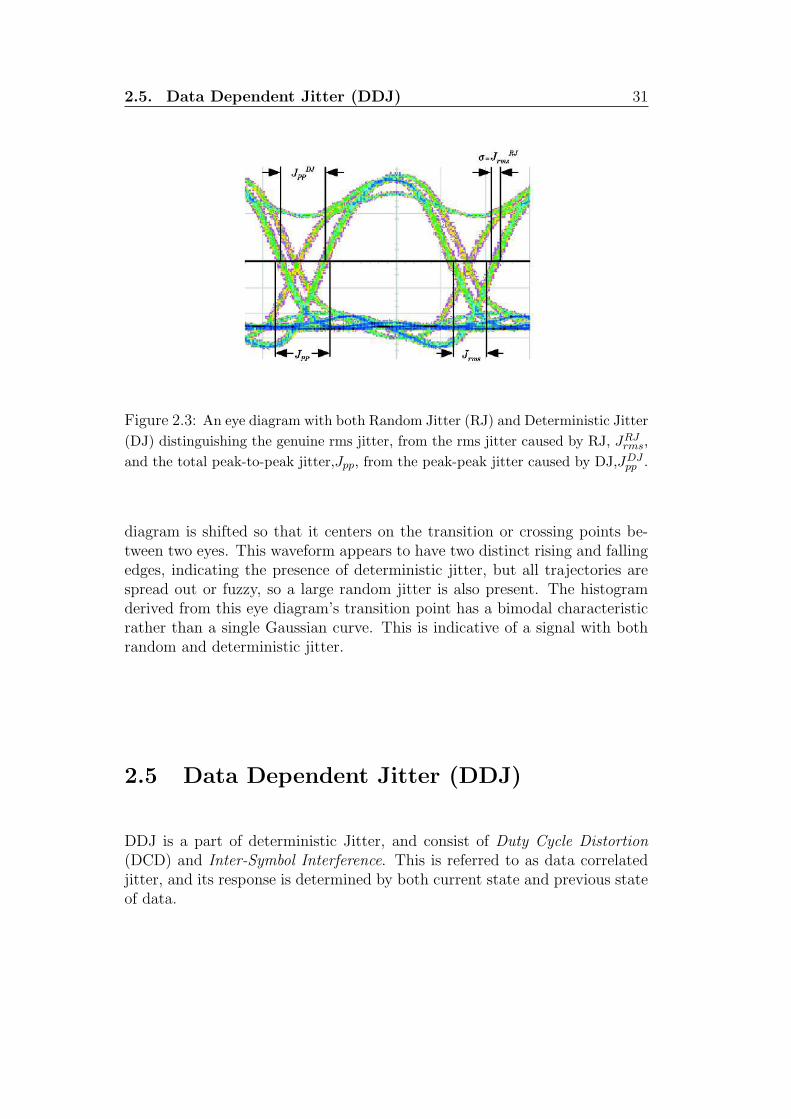
Figure 2.3: An eye diagram with both Random Jitter (RJ) and Deterministic Jitter(DJ) distinguishing the genuine rms jitter, from the rms jitter caused by RJ, JRJ
rms,and the total peak-to-peak jitter,Jpp, from the peak-peak jitter caused by DJ,JDJ
pp .
diagram is shifted so that it centers on the transition or crossing points be-tween two eyes. This waveform appears to have two distinct rising and fallingedges, indicating the presence of deterministic jitter, but all trajectories arespread out or fuzzy, so a large random jitter is also present. The histogramderived from this eye diagram’s transition point has a bimodal characteristicrather than a single Gaussian curve. This is indicative of a signal with bothrandom and deterministic jitter.
2.5 Data Dependent Jitter (DDJ)
DDJ is a part of deterministic Jitter, and consist of Duty Cycle Distortion(DCD) and Inter-Symbol Interference. This is referred to as data correlatedjitter, and its response is determined by both current state and previous stateof data.

32 Chapter 2. Measuring Jitter in digital system
Figure 2.4: Histogram.
2.5.1 Duty Cycle Distortion
The Duty Cycle Distortion1 (DCD) is both the variance in timing away the50% duty cycle, and also the variance in average voltage offset. DCD oc-curs when the transmitter threshold is drifted from its ideal level and conse-quently the edge transition shifted. It is easily observed in the eye diagram asthe nominal eye crossing (where rising edges intersect falling edge) occurringsomewhere other than 50% amplitude point. Fig.2.5 shows a typical DutyCycle distortion. The dotted line shows the ideal output of a transmitterwith an accurate threshold level set at 50% and with a duty cycle of 50%.The solid line waveform represents a distorted output of a transmitter dueto a positive shift in the threshold level. With a positive shift in thresholdlevel, the resultant output signal of the transmitter will have less than 50%duty cycle. If the threshold level is shifted negatively, then the output of thetransmitter will have greater than 50% duty cycle.
Another cause of DCD is asymmetry in rising and falling edge speeds.A slower falling speed relative to the rising edge will result in greater than50% duty cycle for a repeating 1-0-1-0...pattern, and slower rising edge speedsrelative to the falling edge will result in less than 50% duty cycle. The cor-responding results are similar to the previous example, illustrated in Fig.2.5.
1Duty Cycle is the ratio of the pulse duration to the pulse period. Ideally the duty cycleis 50%.

2.5. Data Dependent Jitter (DDJ) 33
Figure 2.5: Duty Cycle Distortion.
2.5.2 Inter Symbol Interference
Another cause of jitter is Inter-Symbol Interference (ISI) [11]. Its main effectis the reduction of the edge speed and so of the amplitudes of the data bitswhich is dependent on repeating-bit lengths and preceding bit states. Obvi-ously this will result in vertical eye closure and in both retarded and advancededges relative to their ideal positions. There are two primary causes of ISI:the bandwidth limitation in either the transmitter or physical media and im-proper impedance termination and physical media discontinuities that causereflections.
Fig.2.6 shows an example of ISI due to bandwidth limitation problems.Limited bandwidth produces limited edge speeds will result in varying pulseamplitudes at high speed data rates. Varying pulse amplitudes will then resultin transition timing errors.
With a long series of repeating ”1’s”, the amplitude of the data signal willeventually rise to a full steady state high level as illustrated by the long-highpulse at point A in fig.2.6. When the state of the data change to a ”0”, thesignal will have a relatively long transition time to reach the threshold level,resulting in a positive timing error. This will be manifested as a positivepeak of timing error in the jitter trend waveform at point B. The negative
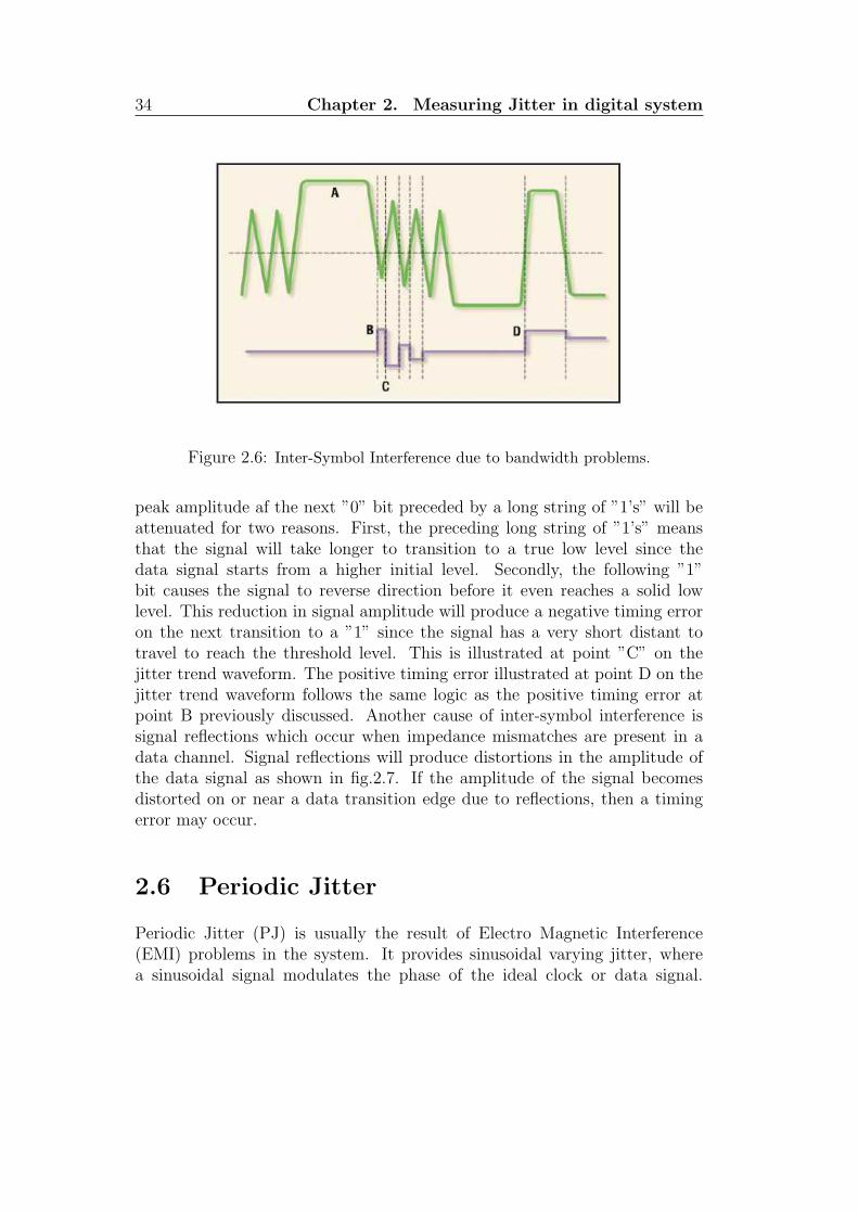
34 Chapter 2. Measuring Jitter in digital system
Figure 2.6: Inter-Symbol Interference due to bandwidth problems.
peak amplitude af the next ”0” bit preceded by a long string of ”1’s” will beattenuated for two reasons. First, the preceding long string of ”1’s” meansthat the signal will take longer to transition to a true low level since thedata signal starts from a higher initial level. Secondly, the following ”1”bit causes the signal to reverse direction before it even reaches a solid lowlevel. This reduction in signal amplitude will produce a negative timing erroron the next transition to a ”1” since the signal has a very short distant totravel to reach the threshold level. This is illustrated at point ”C” on thejitter trend waveform. The positive timing error illustrated at point D on thejitter trend waveform follows the same logic as the positive timing error atpoint B previously discussed. Another cause of inter-symbol interference issignal reflections which occur when impedance mismatches are present in adata channel. Signal reflections will produce distortions in the amplitude ofthe data signal as shown in fig.2.7. If the amplitude of the signal becomesdistorted on or near a data transition edge due to reflections, then a timingerror may occur.
2.6 Periodic Jitter
Periodic Jitter (PJ) is usually the result of Electro Magnetic Interference(EMI) problems in the system. It provides sinusoidal varying jitter, wherea sinusoidal signal modulates the phase of the ideal clock or data signal.

2.7. Bounded Uncorrelated Jitter 35
Figure 2.7: Inter-Symbol Interference due to reflections.
Referring to fig.2.8, in the top is shown a regular clock signal with a 50% dutycycle, in the middle the same clock signal with a sinusoidal phase perturbationat 1/10 the original signal, and with an amplitude of 4/3π, and in the bottoma phase versus time plot of the phase perturbation sinusoid. An example ofPJ would be signals from a switching power supply coupling into the data orsystem clock signals. It is not time-correlated with either the clock or datasignal since it would be based on a different clock source.
Fig.2.9 shows an example of a ”corrupter” signal (upper trace) capacitivelycoupling into our serial data signal (middle trace). This coupling will resultin amplitude distortion on the data signal. If the amplitude distortions occurat or near a data signal transition, a timing error occurs.
2.7 Bounded Uncorrelated Jitter
Bounded Uncorrelated Jitter [12] is commonly caused by crosstalk couplingfrom adjacent interconnects on printed circuit board. It is bounded due tofinite coupling strength, and uncorrelated because there is no correlation tothe channel’own data pattern. In other words, the correlation is with theadjacent traces, not with the trace under study. By definition, crosstalk isthe coupling of energy from one trace to another. This coupling is due to theelectromagnetic field generated by the propagating signals, and its strength

36 Chapter 2. Measuring Jitter in digital system
Figure 2.8: Periodic Jitter (PJ).
is dependent on the physical layout and properties of the traces. Crosstalk iscaused by two main effects: capacitive and inductive coupling.
The crosstalk-induced pulse trace travels both backward toward the nearend, and forward toward the far end of the victim trace, as shown in fig.2.10.The currents due to mutual capacitance propagate toward both the near andfar end of the victim. On the other hand, mutual inductance only drivesthe current from the far end toward the near end in the victim. The totalcrosstalk is the result of the subtraction between inductive and capacitive in-duced pulses. The far end voltage amplitude of the crosstalk can be calculatedfrom
Vpfar =∆Val
√LC
2Tedge
(Lm
L− Cm
C) (2.3)
where ∆Va is the total amplitude change of the aggressor signal, Lm is themutual inductance per unit length, L is the self-inductance per unit length, Cm
is the mutual capacitance per unit length , C is the self-capacitance per unitlength, l is the length of the trace, and Tedge is the edge transition time of theaggressor signal. ∆Va has a positive polarity for a rising edge transition anda negative polarity for a falling edge transition. Fig.2.11 illustrates how thedistorted victim edge transition can occur earlier or later than the distortion-free victim edge transition. If the amplitude of the cross-talk induced pulse isnegative, the distorted victim rising edge will occur later than the distortion-free edge transition, as illustrated in fig.2.11a. On the other hand, if theamplitude of the crosstalk-induced pulse is positive, the distorted victim rising

2.8. Total jitter 37
Figure 2.9: Periodic Jitter (PJ) caused by capacitive coupling.
Figure 2.10: Forward and background propagation
edge will occur earlier, as illustrated in fig.2.11b. The time difference can becalculated from subtracting the edge crossings of the distortion-free and thedistorted victim edge transition.
2.8 Total jitter
The quality of a digital transmission system can be expressed in terms of howmany bits out of transmitted sequence were received in error. The BER isdefined as the number of bits received in error divided by the number of bits

38 Chapter 2. Measuring Jitter in digital system
Figure 2.11: Timing difference due to crosstalk.(a)Distorted edge crossing occurslater then the original edge crossing. (b) Distorted edge crossing occurs earlier thanthe original edge crossing
transmitted
BER =NErr
NBits
(2.4)
To calculate the total jitter on a signal, the components of the Jitter mustbe combined to obtain the expected BER performance. If the individualcomponents are independent it is possible to use a convolution operation tocalculate the distribution which represent the Total jitter
J(x) = PJ(x)⊗DDJ(x)⊗RJ(x) (2.5)
The total jitter distribution is divided in three regions: at the crossing pointthe distribution is dominated by DJ, at time-delays farther from the cross-ing point the distribution is increasingly dominated by RJ until, far from thecrossing point, in the asymptotic limit, the tails follow the Gaussian RJ dis-tribution. The ideal way to determine the behavior of the tails, and hence the

2.8. Total jitter 39
Figure 2.12: A bathtube plot: the bit error ratio as a function of sampling pointdelay, x
TJ(BER) would be to deconvolve RJ and DJ. But without knowing the DJdistribution, there is no practical way to deconvolve the distribution.
2.8.1 Calculating Total Jitter from Bathtub Curves
The goal of the jitter analysis is to determine the effect of the jitter on the BERand ensure that the system BER is less than some maximum value, usually10−12 for many applications. This test is usually done using an error perfor-mance analyzer, commonly referred to as a Bit Error Rate tester or BERT. Abinary sequence (it could be a pseudorandom sequence PRBS) from a patterngenerator is used to modulate the transmission system’s source, while an errordetector compares the received signal with the original transmitted patternand counts for received bits and errors, and calculates the BER. Fig.2.12 showsthe bathtube plot that is a graph of BER versus sampling point throughoutthe unit interval.
BER(x), can also be derived from the jitter distribution, J(x). SinceBER(x) is given by the probability for a logic transition fluctuating acrossthe sampling point time position, x, if we consider the left edge of the eye dia-gram the probability of a transition fluctuating across the point x is given bythe product between the Cumulative Probability Density Function(CDF)2 and
2The CDF provides for each time value the probability that the transition happened

40 Chapter 2. Measuring Jitter in digital system
Figure 2.13: The convolution of the sum of two delta functions separated by DJand a Gaussian RJ distribution of width σ. The underlying assumption of thedual-Dirac approximation is that any jitter distribution can be modeled in thisway.
ρT , the transition density, which is the ratio of the number of logic transitionsto the total number of bits:
BERL(x) = ρT ·∫ +∞
x
J(x′)dx′ (2.6)
The transition density measures 0.500 for a repetitive pattern 0-1-0-1..., and0.4961 for a PBRS7 sequence (pseudorandom bit sequence of length 27 − 1).
Similarly, on the right side of the eye diagram, near x = TB,
BERR(x) = ρT ·∫ −∞
x
J(x′)dx′ (2.7)
so thatBER(x) = BERL(x) + BERR(x) (2.8)
The eye opening at a given BER, t(BER), is given by the separation ofthe left and right BER curves a given BER. For example, in fig.2.12, the eyeopening at BER = 10−12, is given by the difference of xL and xR-those pointswhere BER = 10−12. If we invert BER(x), then
t(BER) = xR(BER)− xL(BER) (2.9)
earlier.

2.8. Total jitter 41
TJ(BER) is the difference in the bit period and the eye opening:
TJ(BER) = TB − t(BER) (2.10)
2.8.2 The Dual-Dirac Model
To calculate the total jitter, DJ could be approximated by a dual-Dirac func-tion [13] [14] that assumes the density function consist of only a pair of deltafunctions. The dual-Dirac Model is an useful tools to estimating the totaljitter at a bit error ratio. It is based on the following assumptions:
• Jitter can be separated into two categories, random jitter (RJ) and de-terministic jitter (DJ).
• RJ follows a Gaussian distribution and can be fully described in termsof a single relevant parameter, the rms value of the RJ distribution or,equivalently, the width of the Gaussian distribution, σ.
• DJ follows a finite, bounded distribution.
• DJ follows a distribution formed by two Dirac-delta functions. Thetime-delay separation of the two delta functions gives the dual-Diracmodel-dependent DJ, as shown in fig.2.13.
The first three assumptions have been described in the previous sections. Thefourth one provides a model which is universally accepted for its utility toquickly estimate the total jitter defined at a bit error ratio. The dual-Diracmodels, provides the simplest possible distribution and it is described by thefollowing equation:
PDF(DJδδ) =1
2[δ(x− µL)− δ(x− µR)] (2.11)
The crossing point is separated into two Dirac delta functions positioned atµL and µR, the DJ dominated region, followed by an an artificially abrupttransition to the RJ dominated tails.
To calculate the total jitter on a signal, the components of the jitter mustbe combined to obtain the expected BER performance.
J(x) = RJ(x)⊗DJ(x) (2.12)

42 Chapter 2. Measuring Jitter in digital system
Q BER
6.4 10−10
6.7 10−11
7.0 10−12
7.3 10−13
7.6 10−14
Table 2.1: Values of QBER, the multiplicative constant for determining eye
closure due to RJ, for different BER values.
where x is the time delay. But the PDF of the Random Jitter is described bya Gaussian whose width is σ.
RJ(x) =1√2πσ
· e− x2
2σ2 (2.13)
Replacing eq.2.11 and eq.2.13 in the eq.2.12
J(x) =1√2πσ
e−x2
2σ2 ⊗ 1
2[δ(x− µL)− δ(x− µR)] (2.14)
The convolution of the sum of two delta functions separated by DJ anda Gaussian RJ distribution of width σ is shown in fig.2.13. The results iscomposed of two Gaussian of width σ separated by a fixed amount DJ(δδ) ≡|µL − µR|.
J(x) =1√2πσ
· (e (x−µL)2
2σ2 + e(x−µR)2
2σ2 ) (2.15)
The eye closure is composed of a fixed amount, DJ(δδ), and an amountthat depends on the bit error ratio of interest. Once σ and DJ(δδ) are mea-sured the eye closure at any BER can be estimated with:
TJ(BER) = 2QBER × σ + DJ(δδ), (2.16)
where QBER is calculated from the complementary error function andDJ(δδ) < JDJ
pp . Since σ is multiplied by 2QBER, the accuracy of the TJ(BER)depends first on the accuracy of the RJ measurement, σ, and second on theaccuracy of the DJ(δδ) measurements. For bounded DJ(x) the asymptoticbehavior of J(x) is the same as that of a Gaussian,
limx→−∞J(x) → Ae−(x−µL)2
2σ2 (2.17)

2.8. Total jitter 43
limx→+∞J(x) → Ae−(x−µR)2
2σ2 (2.18)
so it is possible to estimate TJ(BER) using eq.2.6 and eq.2.7 through eq.2.10.
Figure 2.14: Application of the dual Dirac model to two ideal cases. In (a) thedashed DJ distribution is caused by a single frequency of a sinusoidal jitter and in (b)the dashed bounded, constant (square wave) DJ distribution could be caused by atriangle wave phase modulation. The solid curve is the convolved jitter distributionand the dash-dot lines are the dual Dirac approximation. The vertical line indicatewhere the dual-Dirac model sets the means of Gaussian, µR and µL.
In fig.2.14a the dashed DJ distribution is given by a single frequency ofsinusoidal jitter and, in fig.2.14b, by a flat, bounded DJ distribution. TheDJ distributions are convolved with a Gaussian resulting in the smooth solidcurves. The effect of the convolution is to smooth the sharp edge of the DJdistribution and J(x) obtains its Gaussian tails. The vertical lines in fig.2.14are set µR and µL, demonstrating the inequality, DJ(δδ) = |µR − µL| < JDJ
pp .The two Gaussian curves (dash-dot) give the dual -Dirac approximation to

44 Chapter 2. Measuring Jitter in digital system
the solid curve. Its central part doesn’t match the actual distribution butthe important features is that Gaussian tails match the tails of the true jitterdistribution as in eq.2.17 and eq.2.18 so that TJ(BER) can be estimated usingeq.2.6 and eq.2.7 through eq.2.10.
Chapter 3
The DDR II tester
3.1 Introduction
As discussed in the first chapter, DDR II is the highest-bandwidth memoryavailable today, supporting the threaded applications, improved graphics andmultitasking often found on the most advanced PCs and workstations. Thesememories are elaborately tested by their manufacturers to ensure high qualityproduct for the consumer.
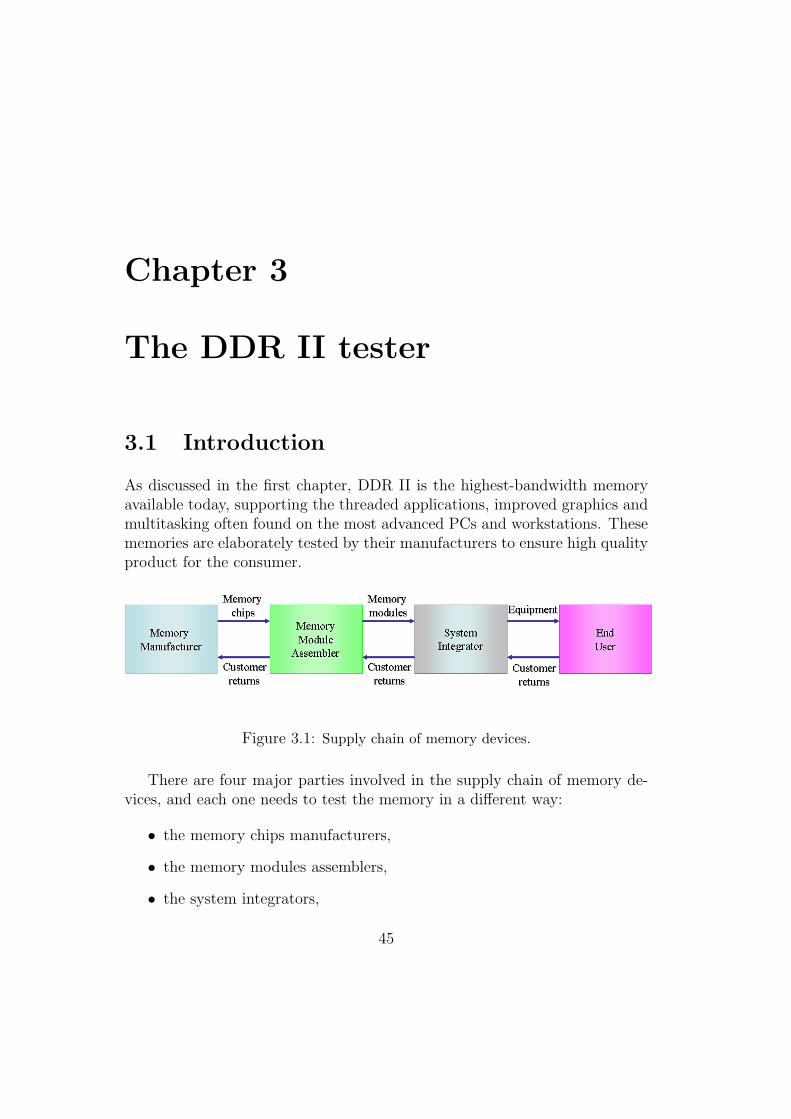
Figure 3.1: Supply chain of memory devices.
There are four major parties involved in the supply chain of memory de-vices, and each one needs to test the memory in a different way:
• the memory chips manufacturers,
• the memory modules assemblers,
• the system integrators,
45

46 Chapter 3. The DDR II tester
• the end user.
Fig.3.1 graphically represents these four parties involved and the way theyinteract. A memory chip manufacturer is the party involved in defining thespecifications of memory devices and subsequently designing and manufactur-ing row memory device of the form shown in fig.3.2. The memory modules
Figure 3.2: Memory chip in TBGA package (source: Infineon Technologies).
assembler is the party that buys memory devices from a memory manufac-turer and implements them into memory modules (fig.3.3) that will be boughtby the system integrator to realize more complex system such as PCs, laptops,workstations or networking equipment.
Figure 3.3: Memory module.
The end user is the party that acquires the equipment provided by thesystem integrator in order to deploy it to solve a specific problem. The bigburden of extensive testing and qualification of memory devices rests on theshoulder of the memory chip manufacturer, the first party in the memorysupply chain. The test done in this phase can be divided in two categories:
• frontend (or wafer level) testing and,

3.1. Introduction 47
• backend (or component level) testing.
Frontend testing is performed before chip packaging so that only functionalchips get to the packaging process, in order to reduce the costs of packaging.Backend testing ensures that packaged chips function properly before deliveryto the customer. The backend test can be further subdivided in more phases:
• Burn-in Test which is a well-known method to check the reliability ofmanufactured components by applying highly stressful operational con-ditions, called test stresses (such as high voltages, possibly combinedwith high temperature), which accelerate the aging process of the mem-ory,
• At Speed Test which has as main objective to check chip functionalitiesat the nominal frequency,
• Parametric Test which is aimed at the validation of electrical parameters(leakage currents, voltage level, rise and fall time, etc.) according to thespecifications.
The memory module assembler performs both the test of the memory device,to verify the specifications declared by the manufacturer, and the test of as-sembled system (checking of the connections, verifying of the terminationsetc.).
The system integrator tests the whole system extensively before deliveryto the end user, because it is expected, in this point of the chain, a very highquality level. Referring to the chip, after the testing process, if the memorydevice are found to cause equipment failure, the defective memories are sentback to the manufacturer in the form of customer returns. The manufactureris then expected to investigate these returns and to try to screen them outbefore they are sold to the memory module assembler.
Finally the end user is not expected to perform any specific testing onacquired systems other than setting them up for regular operation. Here too,the end user sends back defective systems to the integrator in the form ofcustomer returns for reparation or replacement.
A well-known industrial rule of thumb (sometimes referred to as the ruleof tens) on the relative cost of system testing states that at each successivestage in production, it cost ten times as much to identify and repair a defectivecomponent than it would have cost at a previous production stage:
Coststage(i+1) = 10× Coststage(i) (3.1)
48 Chapter 3. The DDR II tester
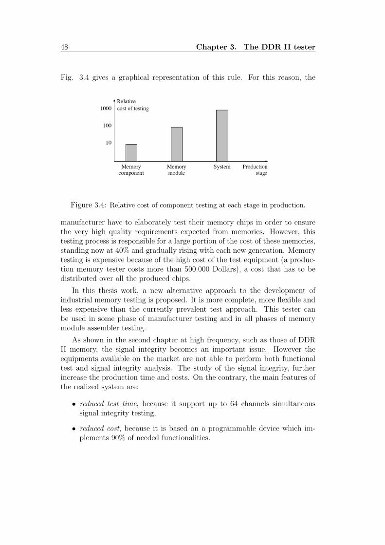
Fig. 3.4 gives a graphical representation of this rule. For this reason, the
Figure 3.4: Relative cost of component testing at each stage in production.
manufacturer have to elaborately test their memory chips in order to ensurethe very high quality requirements expected from memories. However, thistesting process is responsible for a large portion of the cost of these memories,standing now at 40% and gradually rising with each new generation. Memorytesting is expensive because of the high cost of the test equipment (a produc-tion memory tester costs more than 500.000 Dollars), a cost that has to bedistributed over all the produced chips.
In this thesis work, a new alternative approach to the development ofindustrial memory testing is proposed. It is more complete, more flexible andless expensive than the currently prevalent test approach. This tester canbe used in some phase of manufacturer testing and in all phases of memorymodule assembler testing.
As shown in the second chapter at high frequency, such as those of DDRII memory, the signal integrity becomes an important issue. However theequipments available on the market are not able to perform both functionaltest and signal integrity analysis. The study of the signal integrity, furtherincrease the production time and costs. On the contrary, the main features ofthe realized system are:
• reduced test time, because it support up to 64 channels simultaneoussignal integrity testing,
• reduced cost, because it is based on a programmable device which im-plements 90% of needed functionalities.

3.1. Introduction 49
The board, developed in the XS-consulting laboratory, is able to:
• perform the functional test allowing the implementation of any algo-rithm, such as that described in par. 1.7, with high flexibility,
• perform the signal integrity analysis, implementing on each memorychannel, the function of a sampling oscilloscope. This feature perform-ing complex analysis without the use of an external and expensive equip-ment. The complex analysis include the eye opening, rise and fall time,setup and hold time measurements. Moreover it is possible, withoutadditional circuitry, to perform the OCD calibration.
• The voltage, the frequency and the refresh rate can be varied over spec-ified ranges. This feature allows the reconstruction of the Shmoo plotwhich is the graphical display of the response of a component over arange of conditions and inputs. Often it is used to represent the resultsof testing of complex electronic system such as ASICs or microproces-sors. The plot shows the range of conditions in which the device undertest will operate.
The plot is the two dimensional graphical representation of the pass/failbehavior of the memory under the applied test. Fig.3.5 shows an ex-ample of a Shmoo plot, where the x-axis represents the clock cycle timeand the y-axis represents the supply voltage Vdd. The figure shows, forexample, that a lower voltage and a shorter cycle time are the moststressful conditions for the applied test.
Figure 3.5: Shmoo plot showing the cycle time and supply voltage.

50 Chapter 3. The DDR II tester
3.2 Board description
Fig.3.6 and fig.3.7 show respectively the top and bottom of the board. As
Figure 3.6: Tester board:top view.
Figure 3.7: Tester board:bottom view.
shown it can supports:
• DDR II SDRAM memory chips: it is able to test up to eight 8 pinschips or up to four 16 pins chips,

3.2. Board description 51
Figure 3.8: Block diagram of the DDR II tester board.
• DDR II SDRAM memory module: it is able to test up to two 72 pinsmemory modules.
Fig.3.8 details the architecture of the board. A complete system-on-chip ap-proach has been followed in the design of tester. All the functions are imple-mented into a Field Programmable Gate Array (FPGA). This allowed us toreduce the hardware resources and the board dimension and to achieve veryhigh frequency. The FPGA, are quite complex matrices of logical gates, mem-ories and registers with user programmable interconnections. This technologynot only promises new levels of system integration onto a single chip, but italso allows for more features and capabilities in a reprogrammable technology.
The FPGA supplies data, data strobes, controls, addresses and clocks tothe memory chips and memory modules. The memory clocks are synchronousto the FPGA clock.
The board is controlled through a commercial USB interface (QuickUSBQUSB2 plug in module). The QuickUSB QUSB2 Plug-In Module is a 2” ×11/2” circuit board that implements a bus-powered Hi-speed USB 2.0 endpoint

52 Chapter 3. The DDR II tester
terminating in a single 80-pin target interface connector. The target interfaceis shown in the fig.3.9.
As just discussed the board is able to perform any algorithm such as thatdescribed in the par. 1.7. It receives the March element through the USBinterface. The data are moved, through the High Speed Parallel bus, to theFPGA where they are elaborated. The test result is sent back to the USBinterface.
The voltage and frequency of the DDR II chip and DDR II modules canbe varied on a specific range. This feature allows the parametrical analysisas discussed above. The voltage can be varied by the use of a digital po-tentiometer controlled through the SPI port (fig.3.8). The frequency of thechips can be changed, varying the FPGA clock by the use of an external PLL.All the board function are synchronized with respect to a local clock signalgenerated by a programmable PLL driven by a 16MHz oscillator. The PLLis programmable through the SPI port.
Also the Vref of the FPGA is programmable by the use of a digital po-tentiometer through the SPI port. This feature allows the innovative imple-mentation of the sampling oscilloscope that will be described in detail in thefollowing.
The tester board is powered through a 12 V power input line; five non-isolated DC/DC converters derive the voltage source required by the electroniccomponents mounted on the board.
Figure 3.9: Picture of the QuickUSB QUSB2 Plug-In Module and it block diagram.
The following table reports the tester specifications from the electrical andmechanical point of view (area, weight, power consumption):

3.2. Board description 53
• 200× 170 mm2,
• 150 g,
• 1 W.
Figure 3.10: Block diagram of the DDR II tester fpga.
The FPGA used is a VIRTEX 4 device. Manufactured in 1.2v, 90nmtriple oxide technology, VIRTEX-4 FPGA offers twice the performance, twicethe density (it contains up to 200.000 gates) and less than one-half the powerconsumption of previous generation device. It has up to 80 independent clocksand 20 digital clock managers. Differential global clocking minimizes skew andjitter. It has up to 10 Mbits Block RAM with built-in FIFO control logic. TheVIRTEX 4 makes easy to build robust high speed memory interfaces by theuse of the ChipSyncTM technology. This technology provides dedicated highprecision circuits for simplified source synchronous interface. More detailsabout this technology will be done in the following paragraphs.

54 Chapter 3. The DDR II tester
Figure 3.11: Block diagram of the DDR II tester fpga.
3.3 FPGA description
Fig.3.10 shows details about the internal architecture of the FPGA. The DDRII functional tester receives in input from the USB interface the Macro instruc-tion which represent the March element, and gives as output the result of thetest. The Signal integrity analyzer receives in input the data and dqs fromthe DDR II, samples the signals and reconstructs the eye diagram. The Phys-ical layer is responsible for transmitting and receiving all the signals to andfrom the memories. The clocking scheme for this design includes one DCM(Data Clock Manager) and one PMCD (Phase-Matched Clock Divider). Theinternal logic is clocked at half the frequency of the interface. This featurehas allowed us to test chip up to 400MHz (800Mb/s).

3.4. The functional tester 55
The design of the FPGA has been driven by the following guidelines:
• reduce the resources consumed into the FPGA,
• work at the high frequency.
This results in high pipelined and parallel architecture. The overall designrequire 2450 flip-flop and 3745 four input look up table; these correspond tothe 12% and 18% of the available resources. The architecture runs internallyup to 200 MHz clock frequency.
3.4 The functional tester
Fig.3.11 shows details about the functional tester. It receives in input thesequence of commands (WRs and RDs) from USB interface and gives backthe result of the test.Moreover, it provides commands, data and addresses tothe SDRAM. Tab.3.1 lists the commands issued by the controller.
Command Row Address Column Address Write Enable
Select Select Signals
Load Mode L L L
Auto Refresh L L H
Precharge 1 L H L
Bank Activate L H H
Write H L L
Read H L H
No Operation/IDLE H H H
Table 3.1: Commands issued by controller
The commands are detected by the memory using the following controlsignals:
• Row Address Select (RAS)
• Column Address Select (CAS)
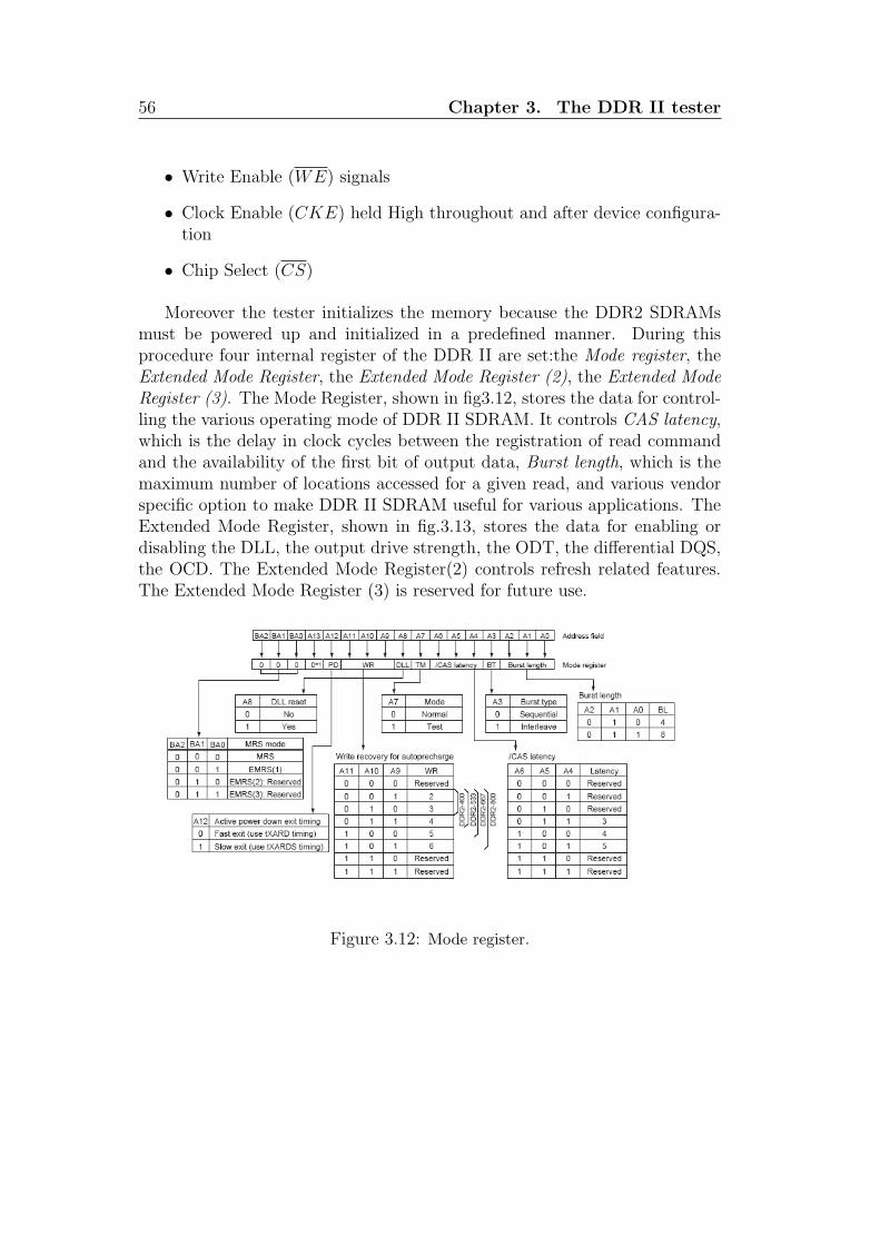
56 Chapter 3. The DDR II tester
• Write Enable (WE) signals
• Clock Enable (CKE) held High throughout and after device configura-tion
• Chip Select (CS)
Moreover the tester initializes the memory because the DDR2 SDRAMsmust be powered up and initialized in a predefined manner. During thisprocedure four internal register of the DDR II are set:the Mode register, theExtended Mode Register, the Extended Mode Register (2), the Extended ModeRegister (3). The Mode Register, shown in fig3.12, stores the data for control-ling the various operating mode of DDR II SDRAM. It controls CAS latency,which is the delay in clock cycles between the registration of read commandand the availability of the first bit of output data, Burst length, which is themaximum number of locations accessed for a given read, and various vendorspecific option to make DDR II SDRAM useful for various applications. TheExtended Mode Register, shown in fig.3.13, stores the data for enabling ordisabling the DLL, the output drive strength, the ODT, the differential DQS,the OCD. The Extended Mode Register(2) controls refresh related features.The Extended Mode Register (3) is reserved for future use.
Figure 3.12: Mode register.

3.4. The functional tester 57
Figure 3.13: Extended Mode register.
3.4.1 March Element Decoder
The March Element Decoder(MED) receives in input the march element, de-codes it and provides the commands, the addresses and data to the next logicstage. Its block diagram is shown in fig.3.14. Referring to the picture, theConfiguration Block is composed of five registers:
• the Operation Code Register, which defines the operations belonging tothe March element. The bit 0 represents the first operation to be done,the bit 1 the second and so on. If Operation Code Register(i)= ’1’ thei-th operation must be done is a WRITE , else it is a READ.

58 Chapter 3. The DDR II tester
Figure 3.14: Block diagram of the March Element Dedoder.
• the N Operation Register, which specifies the number of operations be-longing to the March element,
• the Pattern Register, which contains the pattern must be write or ex-pected in a READ operation.
• the Pattern Code Register, which defines the polarity of the patternrelated to each operation in the ME. The bit0 represents the polarity ofthe pattern related to the first operation to be done, the bit1 representsthe polarity of the pattern related to the second operation and so on. IfPattern Code Register(i)=’1’ the pattern related to the i-th operationis pattern, else it is pattern.
• the Mode Register, which specifies the Functional Mode and the addressorder (UP or DOWN).
The five registers contribute to define the March element. The State Machinesends to the next stage the operations specified in the operation code, then itincreases or decreases the counters according to the functional mode. Thereare two functional modes:
• Column Fast access : for each row address the bank address increasesup to the maximum value, for each bank address the column addressincreases up to the maximum value.

3.4. The functional tester 59
• Row Fast access : for each column address the bank address increases upto the maximum value, for each bank address the row address increasesup to the maximum value.
3.4.2 Command Sequencer
The Command Sequencer(CS) (fig.3.15) receives in input the row address,the column address, the bank address and the commands from MED. As just
Figure 3.15: Block diagram of the Command Sequencer.
discussed in the previous chapter, Read and Write accesses to the DDR IISDRAM device are burst oriented. The burst length which determines themaximum number of locations accessed for a given read is programmable andits possible values are four and eight. The address bits registered with theACTIVE command are used to select the bank and row to be accessed. Theaddress bits registered with the read or write command are used to selectthe bank and the starting column location for the burst access. According tothese specifications the CS activates a row in the corresponding bank if allbanks have been precharged, or it compares the bank and row addresses tothe already open row address and bank address.

60 Chapter 3. The DDR II tester
Figure 3.16: Timing Diagram of the March Element Decoder and Command Se-quencer operations.

3.4. The functional tester 61
Parameter Description t Units
TRP PRECHARGE Command Period 15 ns
TRFC REFRESH to ACTIVE or REFRESH to 75 ns
REFRESH Command Interval
TRCD ACTIVE to READ or WRITE Delay 15 ns
TRAS ACTIVE to PRECHARGE Command 40 ns
TRC ACTIVE to ACTIVE (Same Bank) Command 55 ns
TRTP READ to PRECHARGE Command Delay 7.5 ns
TWTR WRITE to READ Command Delay 7.5 ns
TWR WRITE Recovery Time 15 ns
Table 3.2: Timing Requirements
If there is a conflict, it introduce a PRECHARGE command to prechargethe open bank and then issue an ACTIVE command. Before to issue anycommands the Command Sequencer checks timing requirements according tothe tab.3.2. These parameters are fully programmable through tester. Theyare strictly dependent to the choose component and to its speed grade. Thetab.3.2 refers to a 267 MHz DDR II.
Referring to the Fig.3.16, in the green box are shown the timing of thesignal related to the MED, in the blue box those related to the CS. Thefunctional mode chosen is the Column Fast Access with increasing addressorder. The March element that must be done is ⇑ (w0r0). It correspondsto the the registers settings shown in the picture. The MED has to issue acommand to write the predefined pattern to a given memory location. Afterthe write operation is complete, data has to be read back from the samelocation and compared with the written data. An ACTIVE command isissued to activate the row in the specified bank. After the row has beenopened, the WRITE command has been issued to that row, subject to thetRCD specification. When the CS detects an incoming address referring toa row in a bank other than the currently opened row, the controller issuesa PRECHARGE command to deactivate the open row. It also also issueanother ACTIVE command to the new row (fig.3.16).
The PRECHARGE command is used to deactivate the open row in a

62 Chapter 3. The DDR II tester
particular bank. The bank is available for a subsequent row activation for aspecified time (tRP ) after the PRECHARGE command is issued. The bit10of the bus address determines whether one or all banks are to be precharged.
DDR II devices are required to be refreshed every 7.8µs. The circuit toflag the refresh command is built into the CS. The controller issues the refreshcommand after it completes the transactions in the current open bank.
3.4.3 The Data Path and Physical Layer Interface
The Data path module is responsible for transmitting to and receiving datafrom the memories. Major functions include:
• Writing data to the memory,
• Reading data from the memory,
• Transferring the read data from the memory clock domain to the FPGAclock domain,
• Providing all the necessary control signals to the memory.
Figure 3.17: Clock generation for memory device.
The FPGA generates all the clocks and control signals for reads and writesto memory. As shown in the fig.3.17 the memory clocks are generated using aDouble Data Rate (DDR) register, there is only one clock input to the ODDR.Falling edge data is clocked by a locally inverted version of the input clock.In the fig.3.18 are shown the timing related to the control signals generation.

3.4. The functional tester 63
Figure 3.18: Timing Diagram related to control signals generation.
The Write Data and strobe are clocked out of the FPGA. The strobe mustbe center-aligned with respect to the data (3.19). For DDR II memories, itcould be differential and non-free running, i.e. it is required only when validdata is being written into the memory. The design supports differential andnon-differential data strobe. To meet the requirements specified above thewrite data is clocked out using a clock that is shifted 90 from the primaryclock going to the memory and the data strobes are generated out of primaryclocks going to the memory.
The read and write data path uses the Input Serializer/Deserializer (IS-ERDES) and Output Serializer/Deserializer (OSERDES) features availablein every Virtex-4 I/O. The write data and strobe transmitted by the FPGAuse the OSERDES (fig.3.20). The OSERDES transmits the data (DQ) anddata strobe (DQS) signals. The OSERDES is a dedicated parallel to serialconverter with specific clocking and logic resources designed to facilitate theimplementation of high-speed source synchronous interface.The OSERDEDSconverts 4-bit parallel data at half the frequency of the interface to DDR dataat the interface frequency.

64 Chapter 3. The DDR II tester
Figure 3.19: Write Timing Diagram.
A DDR2 SDRAM interface is source-synchronous, where the read dataand read data strobe are transmitted edge-aligned (fig.3.21). To capture thistransmitted data using Virtex-4 FPGAs, either the strobe or the data canbe delayed. In this design, the read data is captured in the delayed strobedomain and recaptured in the FPGA clock domain in the ISERDES. The re-ceived signal, double data rate (DDR) read data, is converted to 4-bit parallelsingle data rate (SDR) data at half the frequency of the interface using theISERDES. The read data is captured in the delayed strobe domain and re-captured in the FPGA domain. To capture read data without errors the dqsmust be delayed to center in the read data window. Both read and data arefurther delayed to align to the fpga clock domain. To delay the data strobeand read data the FPGA uses a 64 taps absolute delay elements built intoeach IOB, called IDELAY block. The resolution of each tap ia approximately75ps over process, voltage and temperature. This feature provide flexibilityand makes read capture easy. Fig.3.22 shows the block diagram of read datapath module.
To ensure reliable data capture in the DQS domain and recapture in theFPGA clock domain in the ISERDES, a training sequence is required. This se-quence is performed by the calibration block. The controller issues a WRITEcommand to write a data pattern to a specified memory location. The con-troller then issues a back to back read commands to read back the writtendata from this specified location. The outputs of the ISERDES are comparedwith the known data pattern. If they don’t match, DQS is delayed by one tap,and then the comparison is performed again. The tap increments until thereis a match. With the first detected match, the DQS count is incremented to1. DQS continues to be delayed in unit tap increments until a mismatch is

3.4. The functional tester 65
Figure 3.20: Write data path block diagram.
found. The DQS count is also incremented along with the tap increments torecord the width of the data valid windows. DQS is then decremented by halfthe window count to center DQS edge to the center of the data valid win-dow. Fixed the position of the DQS to respect to the DQ valid window, bothdata and strobe are delayed following the same procedure described above.This last step fix the phase of the DQ-DQS to respect the FPGA clock. Thecalibration block also computes the delay in FPGA clock cycles between theregistration of the read command and the first bit of data available. Thisparameter is used in the following read commands.
3.4.4 The Read Data Compare Module
The block diagram of the Read Data Compare Module is shown in fig.3.23.This block receives in input the data from the Physical Layer Interface andcompares it to the expected pattern stored in the Read Data Fifo. Beyondthe Read Data Fifo there is the Segment data fifo. The two fifo are read si-

66 Chapter 3. The DDR II tester
Figure 3.21: Read Timing Diagram.
Figure 3.22: Read data path block diagram.
multaneously. The segment data identifies the segment whose the data belongto. The segment is also the address of an internal RAM which contains theaccumulated errors.
3.5 The Signal Integrity Analyzer
As just discussed in the first chapter the digital errors often have their roots inanalog signal integrity problems. To track down the cause of the digital fault,it is often necessary to turn to an oscilloscope, which can display waveformdetails, edges and noise; can detect and display transients and can help toprecisely measure timing relationships such as setup and hold time.

3.5. The Signal Integrity Analyzer 67
Figure 3.23: Read Data Compare Module.
The signal integrity analyzer (SIA) is designed to provide, on each memorychannel, the functions of a sampling oscilloscope. The oscilloscope is basicallya graph-displaying device, it draws a graph of an electrical signal showinghow the signal change over time: the vertical (y) axis represents voltage andthe horizontal (x) axis represents the time. As a traditional oscilloscope itcreates a waveform point, which is the digital value stored and displayed toconstruct the waveform, by saving one sample point during each waveforminterval. The magnitude of each sample points is equal to the amplitude ofthe input signal at the time in which the signal is sampled. In the following thebasic principle used in this application will be described. The SIA constructs apicture of a signal by making the scanning both in time domain and in voltagerange. Referring to the fig.3.24, the SIA, fixed the threshold , performs a timescanning.
Figure 3.24: Timing Diagram: basic principle used in the Signal Integrity Analyzer.

68 Chapter 3. The DDR II tester
Figure 3.25: Block diagram: basic principle used in the Signal Integrity Analyzer.
A window runs along the time axis.A logic one is detected when the right(left) extreme of the window is below the threshold and the left (right) extremeis above it. When the scanning is complete, the threshold is increased anda new timing scanning performed. The waveform reconstruction is obtainedconnecting the detected ’1s’. However, when measuring high frequency signals,the SIA may not be able to collect enough samples in one sweep. This canbe resolved by taking advantage of the fact that the DQ and DQS, whichare the signals under study, are repetitive signals. This method constructs apicture of a repetitive signal by capturing a sample of the information fromeach repetition. Summarizing the basic element to realize an oscilloscope are(fig.3.25):
• a comparator to compare the input signal with the threshold,
• a digital potentiometer to change the threshold to perform the verticalscanning,
• a programmable delay line to perform the horizontal scanning,
• an edge detector to identify the ’1s’ and ’0s’.
The Virtex-4 device embodies all the components listed above. Fig.3.26shows the block diagram of the Signal Integrity analyzer.
The time shifting and the edge detection are performed by the modules inthe blue box. The Data Clock Manager allows a fine grained phase shifting,i.e., the DCM output clocks can be phase shifted with respect to the input

3.5. The Signal Integrity Analyzer 69
Figure 3.26: Block diagram of the signal integrity analyzer.
clock. The phase shift is programmed by the state machine through a controlsignal named PSINC. A further delay is introduced by the routing of the twoflip flops inside the FPGA. As result one flip flop is clocked with clock+Φ andthe other one is clocked with clock + Φ + ε, ε due to their different positioninside the FPGA. To obtain a known ε the two flip flops are manually routed.
The voltage scanning is obtained varying the Vref of the FPGA. Fig.3.27shows the timing diagram related to the edge detection. Referring to the topside of the picture, the rising edge of the clock + Φ corresponds to a voltagelevel under threshold and thus the logic level of the flip flop output is ’0’,the rising edge of the clock + Φ + ε corresponds to a voltage level over thethreshold resulting in a logic ’1’ at flip flop output. In this case an edge isdetected as shown in the picture. Referring to bottom of the picture, wherethe Φ is unchanged, but the threshold has been moved to the top, both risingedges detect a voltage level under threshold resulting in a logic ’0’ in bothoutputs flip flops. In this case no ’1’ is detected. Referring to the fig.3.26, thestep followed by the internal logic are:
• Fixed the phase Φ, more acquisitions are performed. The detected logic

70 Chapter 3. The DDR II tester
Figure 3.27: Timing Diagram of the edge detection.
’1s’ are stored in the Sync Fifo, which is clocked with the clock of theincoming data. The depth of the Fifo is correlated to the number ofsample (acquisitions) to be acquired.
• The logic ’1s’ from the Sync Fifo are read by the state machine and thenaccumulated. The result is stored in the Line Fifo.
• Φ is incremented and the procedure described above replicated. WhenΦ achieves its maximum value, i.e., the entire line has been scanned,the state machine goes in an IDLE state and wait for a next acquisitioncommand.
To obtain the eye diagram reconstruction a pseudorandom sequence mustbe provided to the SIA. A sequence of pseudorandom patterns are written in

3.5. The Signal Integrity Analyzer 71
all the memory locations of the DDR II SDRAM under test (fig.3.28). Thenthe controller issues a free-running sequence of READ commands providing apseudorandom sequence in input of the SIA. The steps followed to obtain theeye diagram reconstruction are:
1. The Vref of the FPGA is initialized to 0 programming the externaldigital potentiometer through the USB interface and the SPI port,
2. the time scanning is performed. At the end of the scanning the samplingof an entire line is stored inside the internal FIFO,
3. the FIFO is read through the USB interface and the High Speed Parallelport. Then the Vref is incremented and new timing scanning performed.
Figure 3.28: Experimental setup to measure the eye diagram of the dq data duringread operation.
Fig.3.29 shows the eye diagram obtained with the Signal Integrity Analyzerat 266 MHz.

72 Chapter 3. The DDR II tester
Figure 3.29: Eye diagram obtained with the Signal Integrity analyzer at 266 MHz.

Chapter 4
Experimental results
4.1 Introduction
The tester has been successfully tested in the laboratories of the XS-consultinglaboratory in order to verify the foreseen performances. The test was aimedat:
• verifying the tester capability to detect physical defects, first observingthe signals on the interface and after comparing the result of the testingwith those obtained with the traditional tester,
• comparing of the obtained eye diagram with those obtained by the useof a traditional last generation oscilloscope.
4.2 Functional Tester Debug
In order to verify that the tester works according to the specifications, amarch test has been applied and the dq, dqs, clock and command have beenmonitored on the pins of the chip. The test has been performed using a 64×8DDR II SDRAM chip. Custom and low impedance probes has been usedto observe the signals. Fig.4.1 shows the measured waveforms. The clock isrunning at 333MHz.
In the write command (on the left-side) the DQS (selected as single ended)appears at 3 clock cycles after the write command (CAS low) is asserted. In
73

74 Chapter 4. Experimental results
Figure 4.1: Write and Read Operation: dq, dqs, clk and CAS, monitored on thepins of the chip, are shown.
this case the DQS is provided by the controller. The data (sequence 10101010has been chosen), appears center aligned to the dqs, as expected.
In the read command the DQS, provided by the chip, appears at 4 clockcycles after the read command (CAS low) is asserted. The data is edge alignedto the dqs. In both cases CAS latency has been programmed at 4.
In order to debug the tester, a comparison between the functional faultsfound by a traditional tester and those found by the realized equipment hasbeen done. Fig.4.2 (in the bottom side) shows the results obtained testinga chip with known physical defects. The eight green rectangles representsthe eight chips under test. For each rectangle, the rows represent the seg-ments and the columns the byte in each segment. The segment is obtainedcombining some bits of the row address and all bits of the bank address. Inthis implementation the segment is (row13, row12, bank1, bank0). The redsquares identify the defects. Several tests have been done on good chips re-sulting in no errors detections. Fig.4.2 shows also the software interface thathas been used to test the board. Through the software interface is possible toselect between different algorithms (right side). It is possible to observe theeye diagram of the signal under test (left side). The software interface allows

4.2. Functional Tester Debug 75
Figure 4.2: Software Interface.
to program:
• the memory frequency,
• the chip supply voltage,
• the internal memory parameters (CAS latency, Burst length, etc.),
• the timing parameter (tWTR, tRCD, tRRD, etc.),
• the ODT (disable, 50Ω, 75Ω, 150Ω),
• the differential DQS.

76 Chapter 4. Experimental results
Figure 4.3: Experimental setup to measure the eye diagram of the dq data duringwrite operation: the data is observed on special test point positioned near the chip
In order to evaluate the performances in terms of frequency of the board theeye diagram of the data at different frequencies and different value of ODT hasbeen generated. To evaluate the performances is very interesting to observethe signals on the receivers: in the case of write command the receiver is thechip, in the case of the read command the receiver is the controller. In the firstcase the measurements have been done with the use of traditional oscilloscope,LeCroy WAVERUNNER with 1 GHz of bandwidth, in the second case withthe use of the realized tester.
Fig.4.3 shows the setup used for the observation of the signals on the chip(write command). As shown, to obtain the eye diagram a pseudorandom se-quence has been used. To evaluate the integrity of the signal the JEDECspecifications defines an area, or mask, inside the eye diagram. This area isa trapezium with the corners positioned in the point V ref + 250V ,V ref −250V ,V ref +125V ,V ref−125V . To have a good signal integrity the distancebetween the two parallel sides must be at least equal to tsetup + thold defined inthe JEDEC specification. This value is 275ps. Fig.4.4 shows a comparison ofa DDR II DQ bus for a typical SSTL-termination using an ODT terminationversus a non ODT system writing data at 533Mb/s. The most obvious differ-ence between the two buses is the reduction of the over-shoot on the data bus(in the case of the ODT termination). The over-shoot reduction significantlyimproves the voltage margin and reduces Inter-symbol interference (ISI). Thesecond major improvement using DDR II ODT is the increase in the slewrate. Both of these improvements increase the size of the eye diagram. The

4.2. Functional Tester Debug 77
same measurements have been done with different value of frequencies. Theresults have been the same.
Fig.4.5 shows that in the case of 400MHz the presence of the ODT dra-matically increase the size of the eye diagram. In both cases ODT implemen-tation provides improved signal integrity, data eyes, and voltage level marginfor DDR II to enable the systems to attain higher data rates.
In all cases the eye opening is sufficiently large to have a good transmissionof data.
Figure 4.4: Eye diagram measured at chip using 266 MHz clock rate, 1.8-V SSTL-I/O standard, and PRBS8 pattern, and with burst lenght 8, ODT 75Ω(top side)and without ODT(bottom side)

78 Chapter 4. Experimental results
Figure 4.5: Eye diagram measured at chip using 400 MHz clock rate, 1.8-V SSTL-I/O standard, and PRBS8 pattern, and with burst lenght 8, ODT 75Ω(top side)and without ODT(bottom side)
4.3 Signal Integrity Analyzer Debug
Fig.4.6 show the setup used to observe the data with the use of the testerboard. A pseudorandom pattern is written in each memory location. Then acontinuous sequence of read commands are issued by the controller resultingin a pseudorandom sequence at the input of the Signal Integrity Analyzer.Fig.4.7 shows the comparison of the eye diagram obtained by the use of thetester board and the eye diagram obtained with a commercial oscilloscope.

4.3. Signal Integrity Analyzer Debug 79
Figure 4.6: Experimental setup to measure the eye diagram of the dq data duringread operation
Tab.4.1 provides a detailed comparison between the two waveforms. Theslew rate for a rising edge is defined ad the slew rate between the last crossingof V ref − 125V and the first crossing of V ref . The slew rate for a fallingsignal is defined as the slew rate between the last crossing of V ref + 125Vand the first crossing of V ref .
The tester can be use to quickly evaluate the configuration to be used tohave a good signal integrity. Fig.4.8 and fig.4.9 show the eye diagrams of thedq signal respectively in full drive strength configuration and reduced strengthconfiguration. DDR II configured as full drive has a target output impedance
Custom Commercial
Oscilloscope Oscilloscope
horizontal eye opening 1.4ns 1.4ns
vertical eye opening 700mV 700mV
slew rate on falling edge 700mV/ns 700mV/ns
slew rate on rising edge 700mV/ns 700mV/ns
distance between parallel sides 800ps 800ps
Table 4.1: Comparison between the parameters related to the waveforms obtainedby the use of the two oscilloscopes.

80 Chapter 4. Experimental results
Figure 4.7: Comparison between the eye diagram obtained by the use of the boardtester (left side) and those obtained by the use of a traditional oscilloscope.
of approximately 18Ω. When the device is configured as reduced drive thetarget output impedance is approximately 40Ω.
In the full drive configuration the chip driver provides much current thanin the reduced configuration. This results in faster slew rate and higher volt-age levels. In both the figures the eye diagrams have been generated withdifferent values of ODT, respectively 50Ω, 75Ω, 150Ω and without ODT. Anyconfiguration results in a good signal integrity. The slew rate on the risingand falling edges, referred to ODT=75Ω, has been calculate for both the con-figurations (full drive strength and reduced drive strength). In the case offull strength configuration it is 700mV/ns (on the rising and falling edge), inthe case of reduced strength configuration it is 600mV/ns (on the rising andfalling edge), slower as expected. By the fig.4.8 and the fig.4.9 is possible toobserve that the crossing point occurs at 50% of the maximum voltage value.This demonstrate the absence of Duty Cycle Distortion. The result is con-firmed by the measurement of the slew rate on the rising and falling edges(they have the same value).
Similar measurements have been performed for higher frequency. Fig.4.10and Fig.4.11 show the eye diagrams of the dq signal at 400 MHz, respectivelyin full strength configuration and reduced strength configuration. At thishigher frequency the ODT has a big impact on the signal integrity.

4.3. Signal Integrity Analyzer Debug 81
In both cases the signal is affected by the deterministic jitter, ISI. Thisresults in vertical eye closure and in both delayed and advanced edges relativeto their ideal positions. This jitter can be due by the bandwidth limitationof the chip, or improper impedance terminations. The measurements havebeen done at different value of the ODT. Referring to the fig.4.10 only inthe configuration with ODT = 75Ω and ODT = 150Ω the eye opening issufficiently large to guarantee a data transmission without errors. In the casetreated in the fig.4.11 the better configurations are those related to ODT =150Ω and ODT disable. This means that with properly chosen terminationthe effect of the ISI can be reduced.
Figure 4.8: Eye diagram measured at FPGA pin using 266 MHz clock rate, 1.8-VSSTL- I/O standard, and PRBS8 pattern, and with burst lenght 8, in full drivestrength configuration and ODT respectively of 50Ω, 75Ω, 150Ω and without ODT

82 Chapter 4. Experimental results
Figure 4.9: Eye diagram measured at FPGA pin using 266 MHz clock rate, 1.8-VSSTL- I/O standard, and PRBS8 pattern, and with burst lenght 8, in reduced drivestrength configuration and ODT respectively of 50Ω, 75Ω, 150Ω and without ODT

4.3. Signal Integrity Analyzer Debug 83
Figure 4.10: Eye diagram measured at FPGA pin using 400 MHz clock rate, 1.8-V SSTL- I/O standard, and PRBS8 pattern, and with burst lenght 8, with drivestrength full and ODT respectively of 50Ω, 75Ω, 150Ω and without ODT

84 Chapter 4. Experimental results
Figure 4.11: Eye diagram measured at FPGA pin using 400 MHz clock rate, 1.8-V SSTL- I/O standard, and PRBS8 pattern, and with burst lenght 8, with drivestrenght reduced and ODT respectively of 50Ω, 75Ω, 150Ω and without ODT

Conclusions
DDR2 is the highest-bandwidth memory available today, supporting the im-proved graphics and multitasking often found on the most advanced PCs andworkstations. The increasing density and higher frequencies have made thetest processing an important issue to guarantee the reliability of memory op-erations. More and more effort is being dedicated to the study of the faultybehavior of memory devices than ever before. However the testing process isresponsible for a large part of the cost of the memories, standing now at 40%and gradually rising with each new generation.
The realized tester, whose design production and testing is the innovativeissue of this Ph.D thesis work, provides an attractive alternative to the tradi-tional equipment available on the market which are the real responsible of thehigh cost of testing process. Moreover the tester available on the market arenot able to perform a complete and exhaustive analysis without dramaticallyincrease the production costs and time. The realized tester provides:
• fast signal diagnosis, giving the possibility to observe the signal of thechip and its eye diagram. In this way it is easy to find out anomalieson the system supporting the chip such as improper terminations, badconnections or anomaly in the chip such as bandwidth limitation. Bythe observation of the eye diagram is possible to perform a qualitativeanalysis on the Jitter of the signal and so trace the sources of it,
• fast chip diagnosis, finding out the defects on the chips, with high reli-ability.
The innovative issue of this Ph.D thesis work is that 90% of the func-tionalities implemented by the tester have been fitted into a high-speed andhigh-density FPGA. This feature, reducing the hardware resources, dramat-ically decreases the cost of the test equipment and so the production cost of
85

86 Chapter 4. Experimental results
the memory devices. Thanks to a high-pipelined architecture and a specialcare into the place&route phase, high performances in terms of frequency havebeen reached. This feature also reduce the production time of the memorydevices. The tester provides low mass, low power consumption and standardinterfaces.
The realized tester can be introduced in many different manufacturingstages, starting from the initial test application stage performed by the manu-facturers, through the test stage performed by the memory modules assemblersaimed at the verification of the specifications declared by the manufacturersand at the debugging of the assembled system, and ending the memory ramp-up stage where products are shipped to the customer. The tester has beensuccessfully tested comparing the test results with those obtained by the useof more expensive and slower traditional equipment.
Being based on the use of programmable device it could be easily adaptedto the future improvements of the DDR II SDRAM technology.

Bibliography
[1] A. K. Sharma, Semiconductor Memories: Technology, Testing and Relia-bility., New York: IEEE, (1997).
[2] B. Prince, Semiconductor Memories: A Handbook of Design, Manufactureand Application., New York: Wiley, (1991).
[3] Micron Technology Inc., General DDR SDRAM functionality,http://www.micron.com (2001).
[4] Micron Technology Inc., DDR II (Point-to-Point) Features and Function-ality, http://www.micron.com (2003).
[5] Changsik Yoo et al, A 1.8-V 700-Mb/s/pin 512-Mb DDR II SDRAM withOn-Die Termination and Off-Chip Driver Calibration, IEEE Journal ofSolid State Circuit, vol.39, no.6, June 2004.
[6] Elpida Memory, Inc.,How to use DDR2 SDRAM,http://www.elpida.com(2004)
[7] Agilent Technologies, M. Mueller, R.Stephens, R. McHugh, Total Jit-ter Measurement at Low Probability Levels, Using BERT Scan Method,http://www.agilent.com (2005).
[8] Agilent Technologies, Measuring Jitter in Digital System,http://www.agilent.com (2003).
[9] Agilent Technologies,Greg LeCheminant,How to take the evil out of eyediagrams, http://www.agilent.com (2002).
[10] Agilent Technologies, Jitter Analysis Techniques for High Data Rates,http://www.agilent.com (2003).
87

88 BIBLIOGRAPHY
[11] Agilent Technologies,Finding Sources of Jitter with Real Time JitterAnalysis, http://www.agilent.com.
[12] A.Kuo, R.Rosales, T.Farahmand, S.Tabatabaei and Andre Ivanov,Crosstalk Bounded Uncorrelated Jitter (BUJ) for High Speed In-terconnect,IEEE Transactions on Instrumentation and measurement,vol.54,no.5,October 2005.
[13] Agilent Technologies, Jitter Analysis: The dual-Dirac Model, RJ/DJ,and Q-scale, http://www.agilent.com (2004).
[14] Marcel A.Kossel and Martin L.Schmatz, Jitter Measurements of High-Speed Serial Links, IEEE Design and Test of Computers (2004).